asic physical design post-layout verificationnelson/courses/elec5250_6250/slides/asic...asic...
TRANSCRIPT

ASIC Physical DesignPost-Layout Verification

ASIC Physical Design (Standard Cell)(can also do full custom layout)
FloorplanChip/Block
Place & RouteStd. Cells
Component-Level Netlist (Verilog)
IC Mask Data
Design RuleCheck
Std. CellLayouts Cadence:
Encounter(std cells)
Virtuoso(chip assembly)
SPICE/ADiT Simulation Model
BackannotateSchematic
GenerateMask Data
Layout vs.Schematic
Check
Design RulesProcess Data
Libraries
Calibre Calibre Calibre
ICblocks
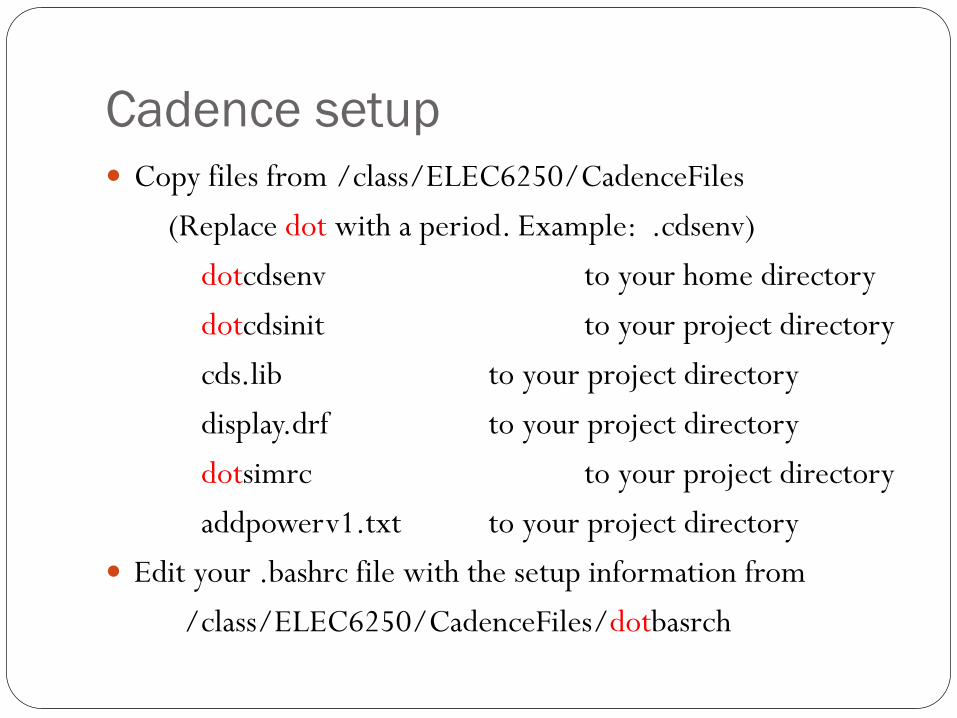
Cadence setup Copy files from /class/ELEC6250/CadenceFiles
(Replace dot with a period. Example: .cdsenv)dotcdsenv to your home directorydotcdsinit to your project directorycds.lib to your project directorydisplay.drf to your project directorydotsimrc to your project directoryaddpowerv1.txt to your project directory
Edit your .bashrc file with the setup information from/class/ELEC6250/CadenceFiles/dotbasrch

Import digital block into Virtuoso Import GDSII layout information into Virtuoso: Encounter saves: mydesign.gds2 Import into a Cadence library File > Import > Stream
Results in cell “layout” view
Import circuit netlist into Virtuoso: Gate-level netlist saved by Encounter: mydesign.v Import netlist into a Cadence Library File > Import > Verilog
Results in cell “schematic” and “symbol” views Gates replaced by transistors using “cdslib” components
(Demonstration)
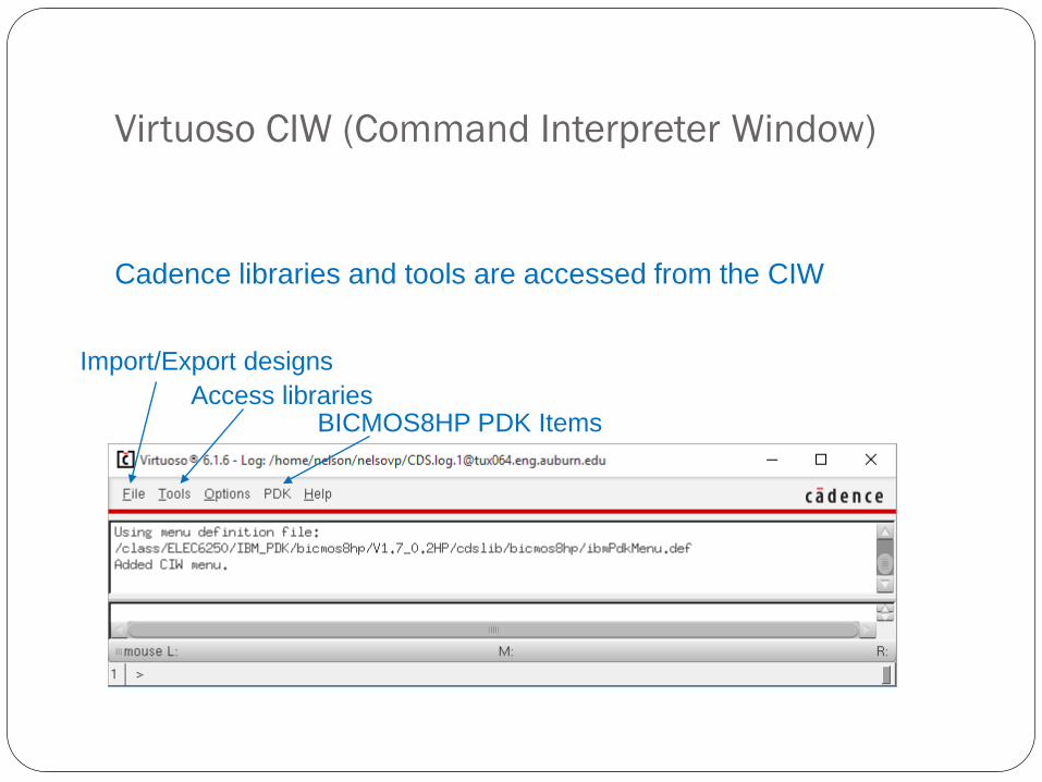
Virtuoso CIW (Command Interpreter Window)
Cadence libraries and tools are accessed from the CIW
Import/Export designsAccess libraries
BICMOS8HP PDK Items
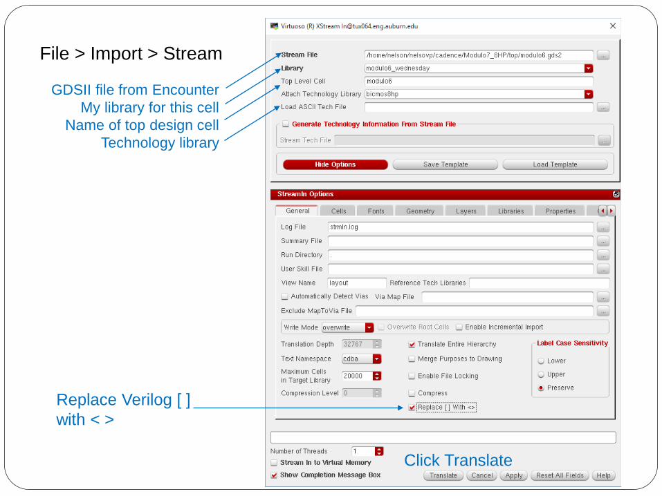
File > Import > Stream
GDSII file from EncounterMy library for this cell
Name of top design cellTechnology library
Replace Verilog [ ]with < >
Click Translate
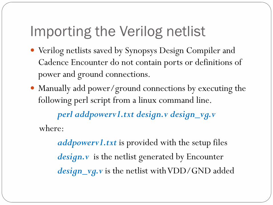
Importing the Verilog netlist Verilog netlists saved by Synopsys Design Compiler and
Cadence Encounter do not contain ports or definitions of power and ground connections.
Manually add power/ground connections by executing the following perl script from a linux command line.
perl addpowerv1.txt design.v design_vg.v
where:addpowerv1.txt is provided with the setup filesdesign.v is the netlist generated by Encounterdesign_vg.v is the netlist with VDD/GND added

Generated Verilog netlistmodule modulo6 (VDD, VSS,
CLEARbar, L_Cbar, CLK, I, Q);
inoutVDD, VSS;input CLEARbar; input L_Cbar; input CLK; input [2:0] I; output [2:0] Q;
Power/ground added
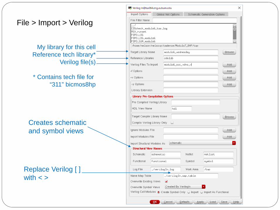
File > Import > Verilog
My library for this cellReference tech library*
Verilog file(s)
* Contains tech file for “311” bicmos8hp
Replace Verilog [ ]with < >
Creates schematicand symbol views
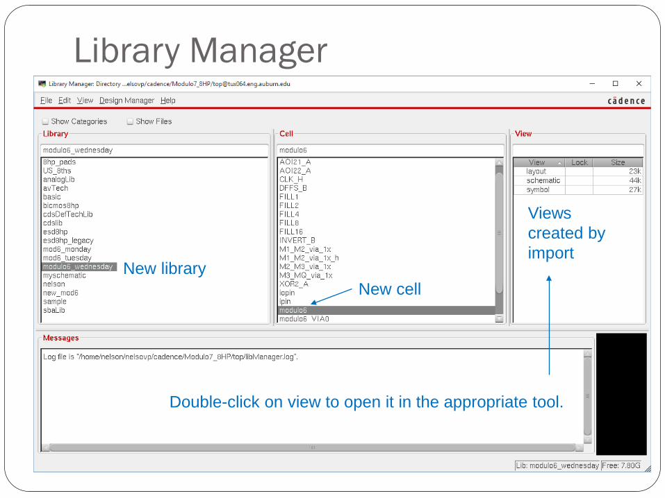
Library Manager
New libraryNew cell
Viewscreated byimport
Double-click on view to open it in the appropriate tool.
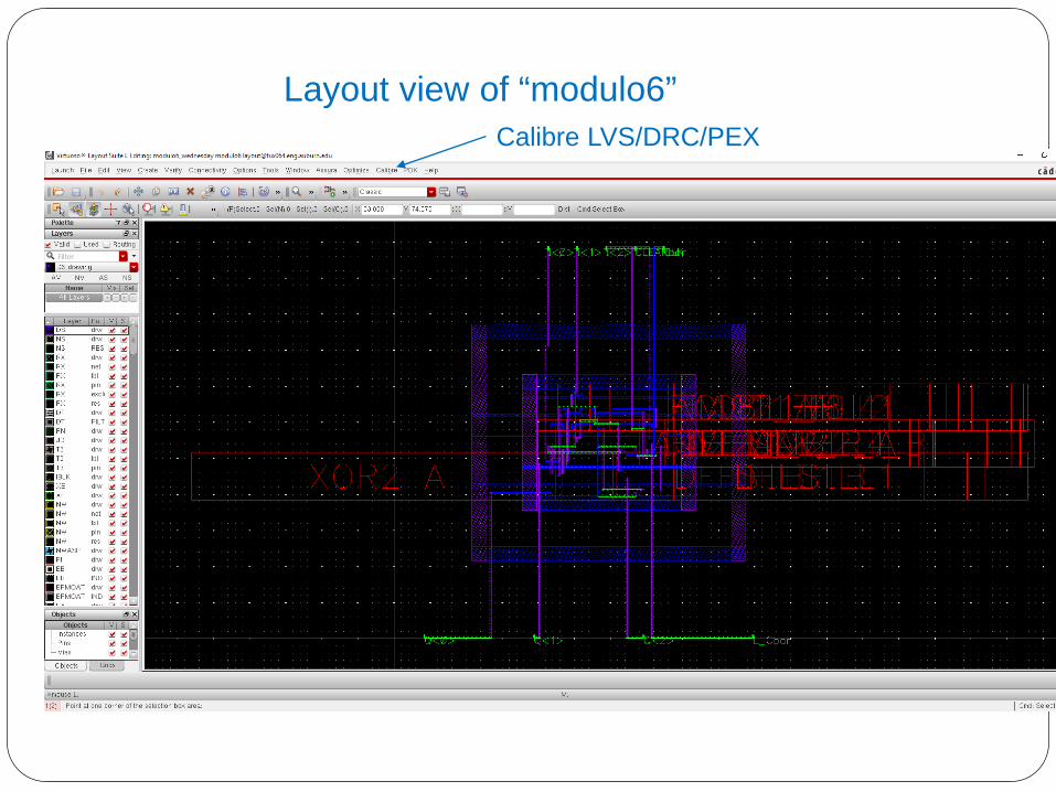
Layout view of “modulo6”Calibre LVS/DRC/PEX

Schematic view of “modulo6”
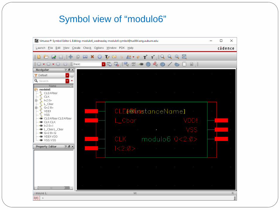
Symbol view of “modulo6”

Verify correctness of layout Open layout in Virtuoso Verify with Calibre or Assura tools
1. LVS (layout vs. schematic) Extract netlist from layout Compare extracted netlist to imported netlist
2. DRC (design rule check) Checks all layout levels Errors should be fixed as appropriate
3. PEX (parameter extraction) Extract netlist from layout, including R/C parameters Simulate netlist to verify functionality and timing
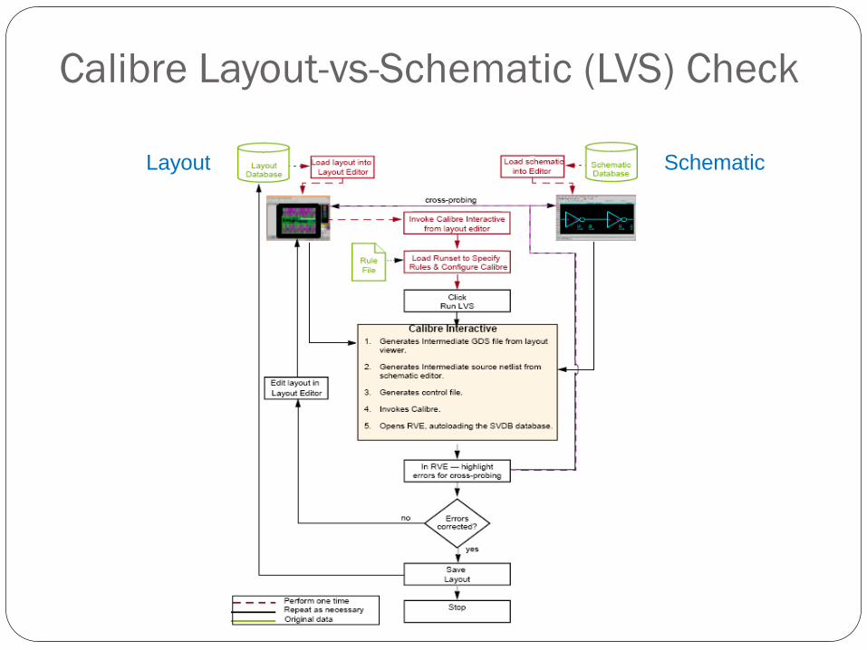
Calibre Layout-vs-Schematic (LVS) Check
Layout Schematic

Layout vs schematic check(Calibre Interactive LVS)
Compares extracted transistor-level netlist vs. netlist generated from Verilog gate-level netlist
From Layout GXL menu: Calibre > Run LVS(Demonstrate )
Mentor Graphics LVS Rules: $ADK/technology/ic/process/tsmc035.calibre.rules Inputs/Layout: will be generated by Calibre Inputs/Netlist: count4.src.net (created in DA-IC)
Top-level cell: count4 (schematic name) Inputs/H-cells (hierarchical cells): $ADK/technology/adk.hcell Extracted file: count4.lay.net
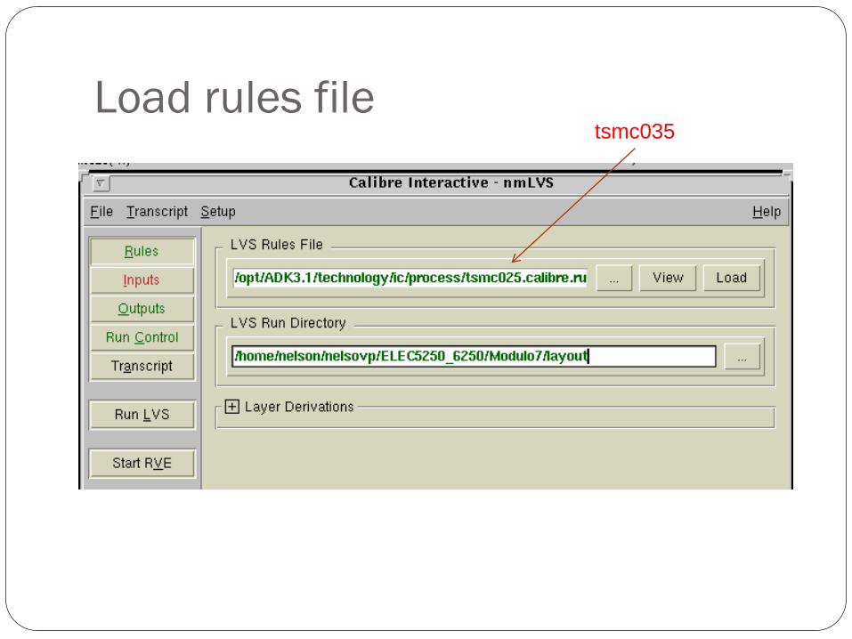
Load rules filetsmc035

Calibre inputs
Layout to be extractedby Calibre (GDSII format)
Layout top cell name
Extracted layout netlist
Source netlist created in DA-IC
Schematic name
Hierarchical cells file:$ADK/technology/adk.hcell
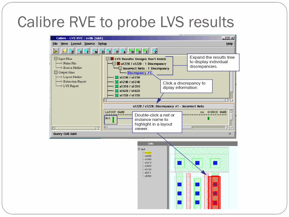
Calibre RVE to probe LVS results

Post-layout functional/timing verification (Calibre PEX) Purpose: timing analysis & functional verification of the final
design analyze netlist extracted from layout parasitic wire capacitance parasitic wire to wire capacitance net and via resistance
perform netlist & parameter extraction with Calibre PEX simulate in ADiT, Eldo, Spectre, PSPICE, HSPICE, etc.
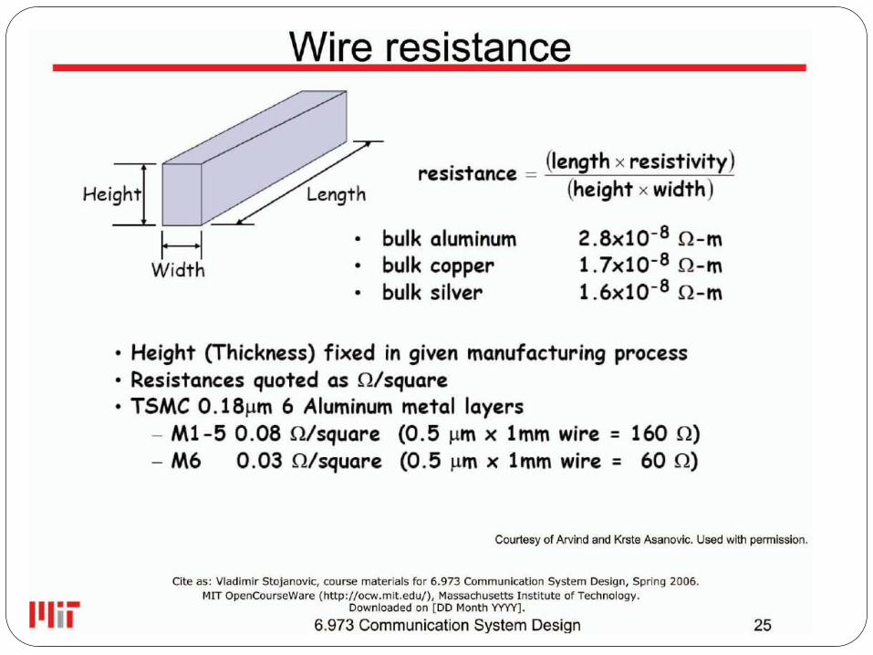
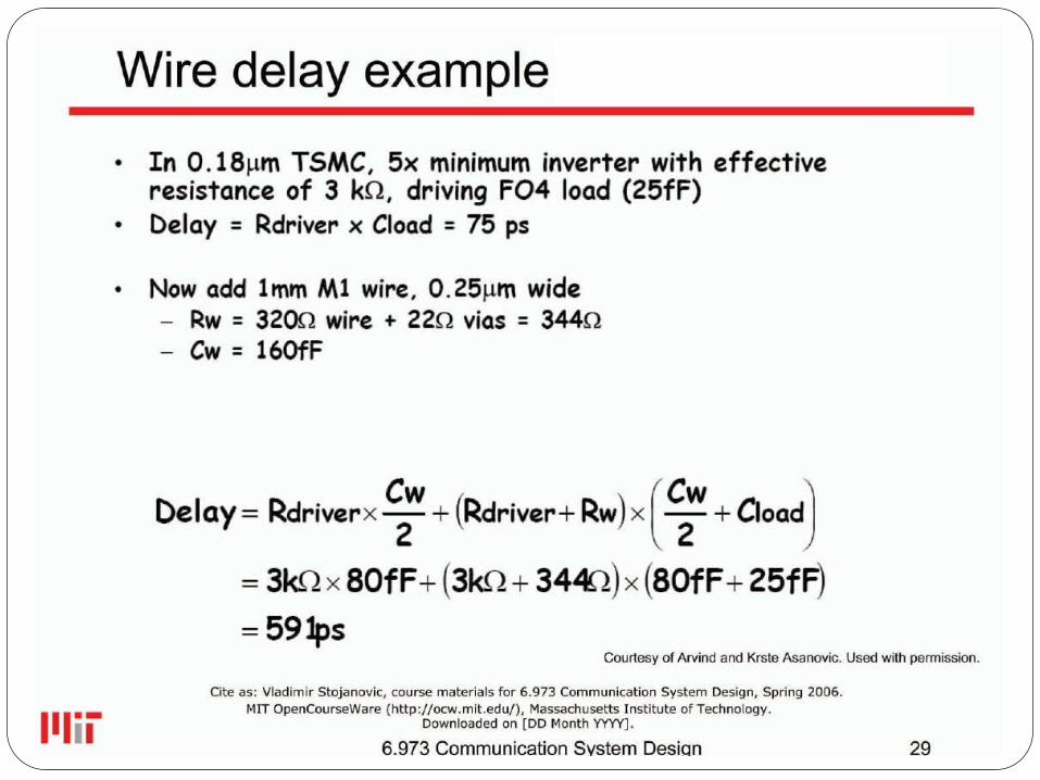
Wire delay estimation
0 0.5 1 1.5 2 2.5 3 3.5 4 4.5 50
0.5
1
1.5
2
2.5
time (nsec)
volta
ge (V
)
x= L/10
x = L/4
x = L/2
x= L
Diffused signal propagation
Delay ~ L2
CN-1 CNC2
R1 R2
C1
Tr
Vin
RN-1 RN
The distributed RC-line


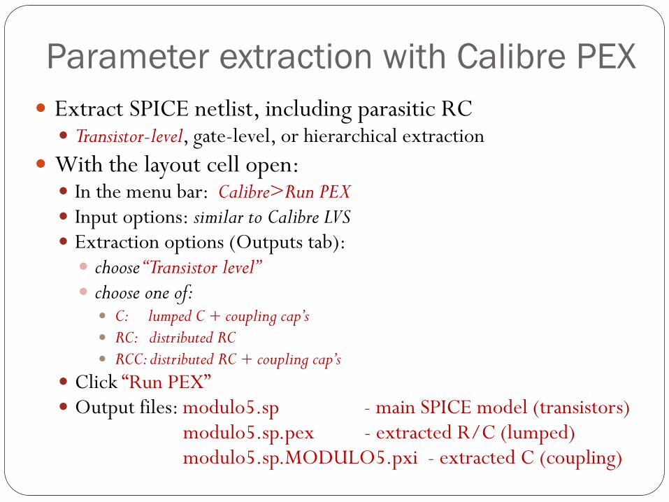
Parameter extraction with Calibre PEX Extract SPICE netlist, including parasitic RC Transistor-level, gate-level, or hierarchical extraction
With the layout cell open: In the menu bar: Calibre>Run PEX Input options: similar to Calibre LVS Extraction options (Outputs tab): choose “Transistor level” choose one of:
C: lumped C + coupling cap’s RC: distributed RC RCC: distributed RC + coupling cap’s
Click “Run PEX” Output files: modulo5.sp - main SPICE model (transistors)
modulo5.sp.pex - extracted R/C (lumped)modulo5.sp.MODULO5.pxi - extracted C (coupling)

Extracted file – top level
Include extracted R/C
N transistorsource drain bulk gate
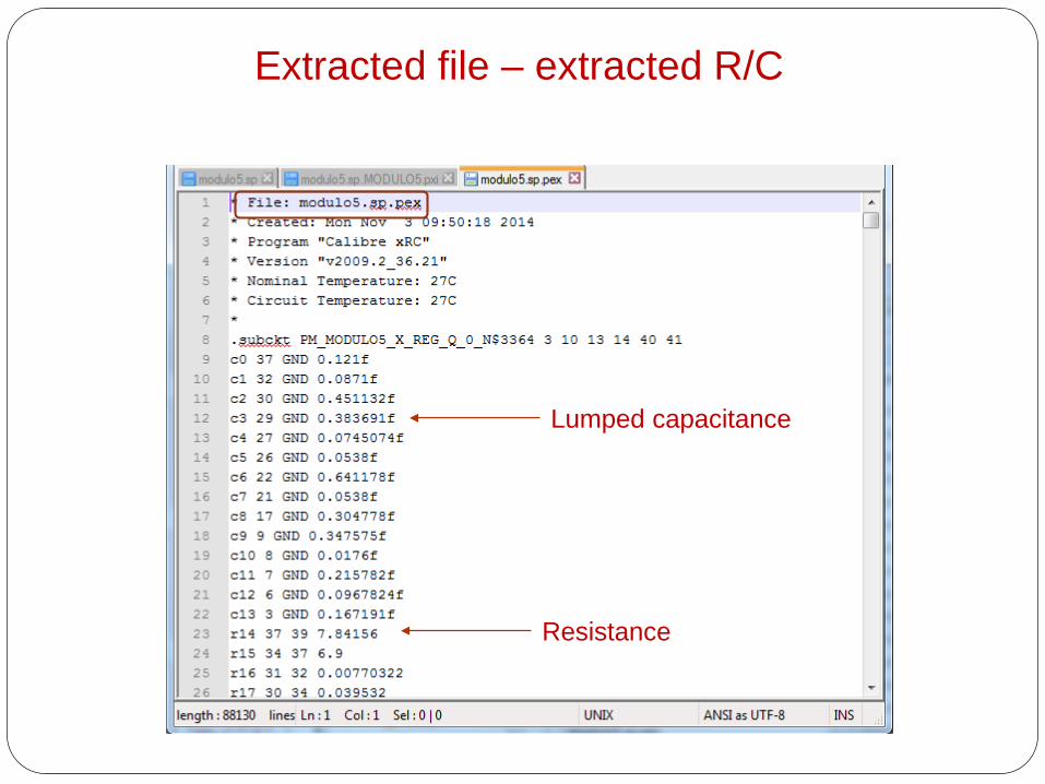
Extracted file – extracted R/C
Lumped capacitance
Resistance
Calibre PEX inputs
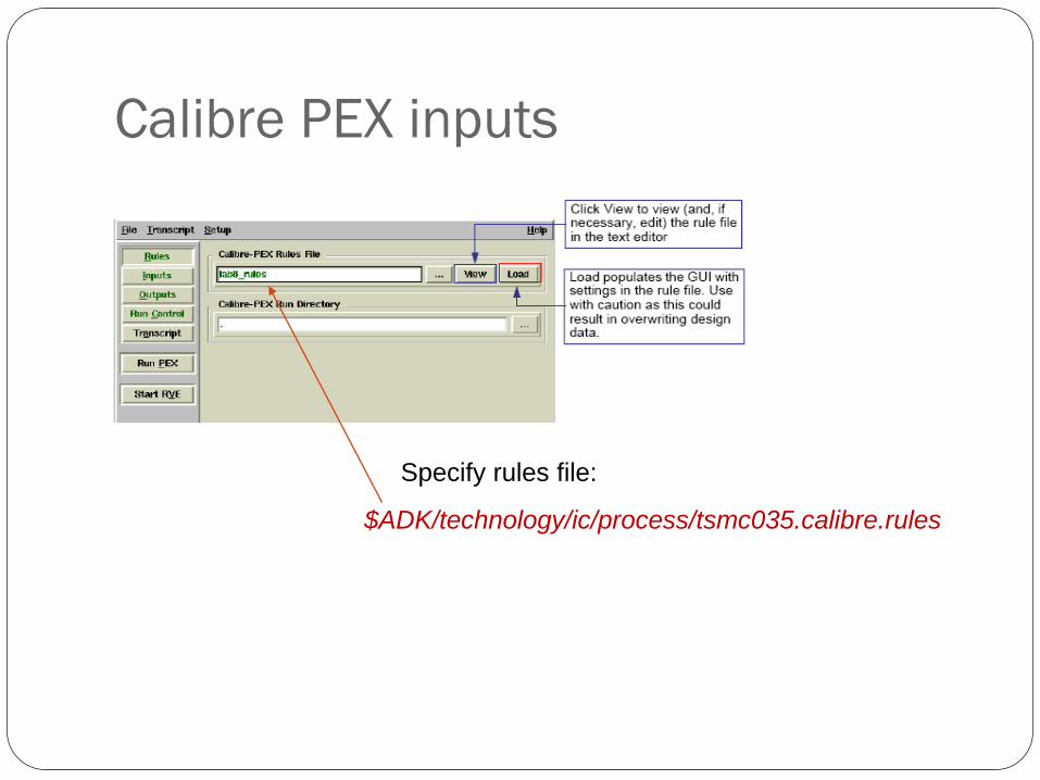
Specify rules file:
$ADK/technology/ic/process/tsmc035.calibre.rules

Calibre PEX inputs
Source(SPICE) netlist created in DA-IC
Top-level cell name in SPICE netlist
Hierarchical cells file:$ADK/technology/adk.hcell
Specify rule file:Name of layout file (count4.gds)GDSII file formatCheck to generate new layout fileName of top cell (count4)

Calibre PEX netlist output
Use net namesfrom LAYOUT
Lumpedcapacitance
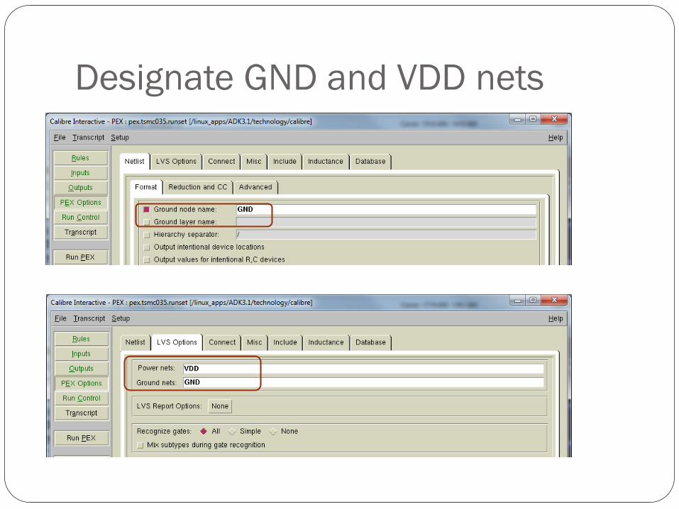
Designate GND and VDD nets