as7265x multi spectral chipset - ams.com
TRANSCRIPT

Application Note DN[Document ID]
ams Application Note Page 1
[v1-03] 2017-Mar-15 Document Feedback
AS7265x Multi Spectral Chipset
Design Considerations

AS7265x
Design Considerations
ams Application Note Page 2
[v1-03] 2017-Mar-15 Document Feedback
Content Guide
1 General Description ............................................................................................................. 3
2 AS7265x Multispectral Chipset ............................................................................................ 3
3 Hardware Design Considerations ........................................................................................ 4
3.1 Pin Description ..................................................................................................................... 4
3.2 Typical Schematic ................................................................................................................ 5
3.3 UART Interface .................................................................................................................... 5
3.4 I2C Interface ......................................................................................................................... 6
3.5 Light Source Selection ......................................................................................................... 7
3.6 Other Connections ............................................................................................................... 7
3.7 PCB Layout Considerations ................................................................................................. 7
3.8 Optic Considerations ............................................................................................................ 9
4 Software Design Considerations .......................................................................................... 9
4.1 Features and Register Structure .......................................................................................... 9
4.2 I2C Virtual Register Read ................................................................................................... 10
4.3 I2C Virtual Register Write ................................................................................................... 11
5 Contact Information ............................................................................................................ 14
6 Copyrights & Disclaimer ..................................................................................................... 15
7 Revision Information .......................................................................................................... 16
AS7265x
Design Considerations
ams Application Note Page 3
[v1-03] 2017-Mar-15 Document Feedback
1 General Description
This Application Note briefly describes system level design considerations with ams AS7265x
Multispectral Chipset solution.
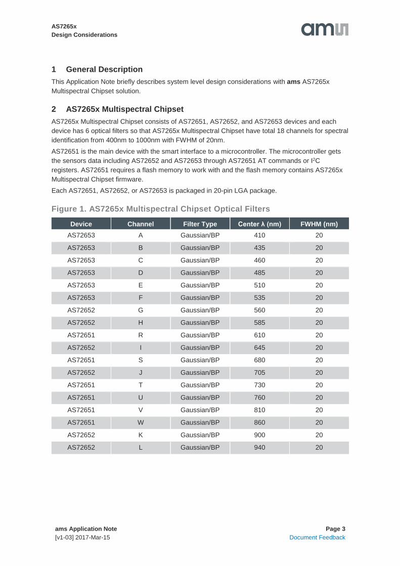
2 AS7265x Multispectral Chipset
AS7265x Multispectral Chipset consists of AS72651, AS72652, and AS72653 devices and each
device has 6 optical filters so that AS7265x Multispectral Chipset have total 18 channels for spectral
identification from 400nm to 1000nm with FWHM of 20nm.
AS72651 is the main device with the smart interface to a microcontroller. The microcontroller gets
the sensors data including AS72652 and AS72653 through AS72651 AT commands or I2C
registers. AS72651 requires a flash memory to work with and the flash memory contains AS7265x
Multispectral Chipset firmware.
Each AS72651, AS72652, or AS72653 is packaged in 20-pin LGA package.
Figure 1. AS7265x Multispectral Chipset Optical Filters
Device Channel Filter Type Center λ (nm) FWHM (nm)
AS72653 A Gaussian/BP 410 20
AS72653 B Gaussian/BP 435 20
AS72653 C Gaussian/BP 460 20
AS72653 D Gaussian/BP 485 20
AS72653 E Gaussian/BP 510 20
AS72653 F Gaussian/BP 535 20
AS72652 G Gaussian/BP 560 20
AS72652 H Gaussian/BP 585 20
AS72651 R Gaussian/BP 610 20
AS72652 I Gaussian/BP 645 20
AS72651 S Gaussian/BP 680 20
AS72652 J Gaussian/BP 705 20
AS72651 T Gaussian/BP 730 20
AS72651 U Gaussian/BP 760 20
AS72651 V Gaussian/BP 810 20
AS72651 W Gaussian/BP 860 20
AS72652 K Gaussian/BP 900 20
AS72652 L Gaussian/BP 940 20

AS7265x
Design Considerations
ams Application Note Page 4
[v1-03] 2017-Mar-15 Document Feedback
Figure 2. Typical Spectral Responsivity
3 Hardware Design Considerations
3.1 Pin Description
Figure 3. Pin Description
Pin AS72651 AS72652/AS72653
Name Description Name Description
1 SDA_M Digital Input/Output; I2C Master Data NC No Connect
2 RESN Digital Input; Reset, Active Low Same as AS72651
3 SCK Digital Output; SPI Serial Clock NC No Connect
4 MOSI Digital Input/Output; SPI MOSI NC No Connect
5 MISO Digital Input/Output; SPI MISO NC No Connect
6 CSN_EE Digital Output; Chip Select for Flash
Memory NC No Connect
7 CSN_SD Digital Output; Chip Select for SD Card NC No Connect
0
0,1
0,2
0,3
0,4
0,5
0,6
0,7
0,8
0,9
1
35
0
37
4
39
8
42
2
44
6
47
0
49
4
51
8
54
2
56
6
59
0
61
4
63
8
66
2
68
6
71
0
73
4
75
8
78
2
80
6
83
0
85
4
87
8
90
2
92
6
95
0
97
4
99
8
No
rmal
ized
Res
po
nsi
vity
Wavelength (λ, nm)
18 Channel Spectral_ID ResponseAS72651 + AS72652 + AS72653
410nm
435nm
460nm
485nm
510nm
535nm
560nm
585nm
610nm
645nm
680nm
705nm
730nm
760nm
810nm
860nm
900nm
940nm

AS7265x
Design Considerations
ams Application Note Page 5
[v1-03] 2017-Mar-15 Document Feedback
Pin AS72651 AS72652/AS72653
Name Description Name Description
8 I2C_ENB Digital Input; Interface Selection NC No Connect
9 INT Digital Output; Interrupt active Low SCL_S I2C Slave
10 NC No Connect SDA_S I2C Slave
11 RX/SCL_S Digital Input; Interface Pin NC No Connect
12 TX/SDA_S Digital Input/Output; Interface Pin NC No Connect
13 ADDR Digital Output (Open Drain); Set Address NC No Connect
14 VDD2 Voltage Supply; Same as AS72651
15 LED_DRV Analog Output; LED Driver Output Same as AS72651
16 GND Supply; Ground Same as AS72651
17 VDD1 Voltage Supply; Same as AS72651
18 LED_IND Analog Output; LED Driver for Indicator Same as AS72651
19 NC No Connect Same as AS72651
20 SCL_M Digital Output; I2C Master Clock NC No Connect
3.2 Typical Schematic
The typical schematic in Figure 4 shows AS72651, AS72652, and AS72653 connections. The
supply voltage to AS72651, AS72652, and AS72653 should be 3.3V ± 10%.
Either UART interface or I2C interface can be used by the controller to get the sensors data.
Figure 4. Typical Schematic
3.3 UART Interface
AS72651 has an UART interface to communicate to the controller. AT commands can be used for
data acquisition, sensors configuration, and LED drivers control. Please refer to AS72651 data
sheet for complete AT commands.

AS7265x
Design Considerations
ams Application Note Page 6
[v1-03] 2017-Mar-15 Document Feedback
Pin11 of AS72651 is the RX of UART, which AS72651 receives the information from the controller.
Pin12 of AS72651 is the TX of UART, which AS72651 transmits the information to the controller.
Any Windows terminal application with baud rate 115200, 8 data bit, 1 stop bit, and none parity can
be used for AT commands.
Since pin11 and pin12 of AS72651 are also shared with I2C interface, the pin8, I2C_ENB, has to be
pulled down for UART interface configuration.
3.4 I2C Interface
AS72651 has both I2C master and I2C slave interface. Both support I2C fast mode (400 KHz) and
standard mode (100 KHz).
AS72651 I2C slave interface is used for communication to the controller. The pin11, SCL_S, is
assigned to the I2C bus clock and the pin12, SDA_S, is for the bus data. The pin8, I2C_ENB, has to
be pulled HIGH.
AS72651 I2C master interface is used for controlling AS72652 and AS72653. The pin20, SCL, is the
I2C bus clock and the pin1, SDA, is for the I2C bus data. The communication between AS72651 and
AS72652/AS72653 is managed by the firmware.
According to I2C specification, both SCL and SDA are open drain and need to be connected to a
positive supply voltage via a pull-up resistor. The pull-up resistors, R13/R14 in the typical
schematic, pull the line high when it is not driven low by the open drain interface. The maximum
value of the pull-up resistor is limited by the bus capacitance, 𝐶𝑏, and the rise time, 𝑡𝑟, as below.
𝑅𝑃(𝑚𝑎𝑥) =𝑡𝑟
(0.8473 ∗ 𝐶𝑏)
The bus capacitance is the total capacitance of wire, connections, and pins. I2C Bus specifies the
maximum rise time is 300ns.
On the other hand, the minimum value of the pull-up resistor depends on the device logical
specifications and allows 𝑉𝑂𝐿 level to be read as a valide logical low.
𝑅𝑃(𝑚𝑖𝑛) =𝑉𝐷𝐷 − 𝑉𝑂𝐿(𝑚𝑎𝑥)
𝐼𝑂𝐿
For the AS7265x Multispectral Chipset application with 3.3V supply voltage, 0.4V maximum 𝑉𝑂𝐿,
and the specified minimum sink current of 3mA for standard mode (100 KHz) or fast mode (400
KHz), the minimum pull-up resistor value is 966.7Ω.
Then the decision of the pull-up resistor value would be based on the rise time, the total bus
capacitance, and the power budget. A smaller resistor may get short rise time but has higher power
consumption.
Please note, the typical schematic here is configured as UART interface by default so there are no
pull-up resistors on AS72651 I2C slave interface. If I2C slave interface is needed, please add the
pull-up resistors on either the controller side or on AS72651 I2C interface.
AS7265x
Design Considerations
ams Application Note Page 7
[v1-03] 2017-Mar-15 Document Feedback
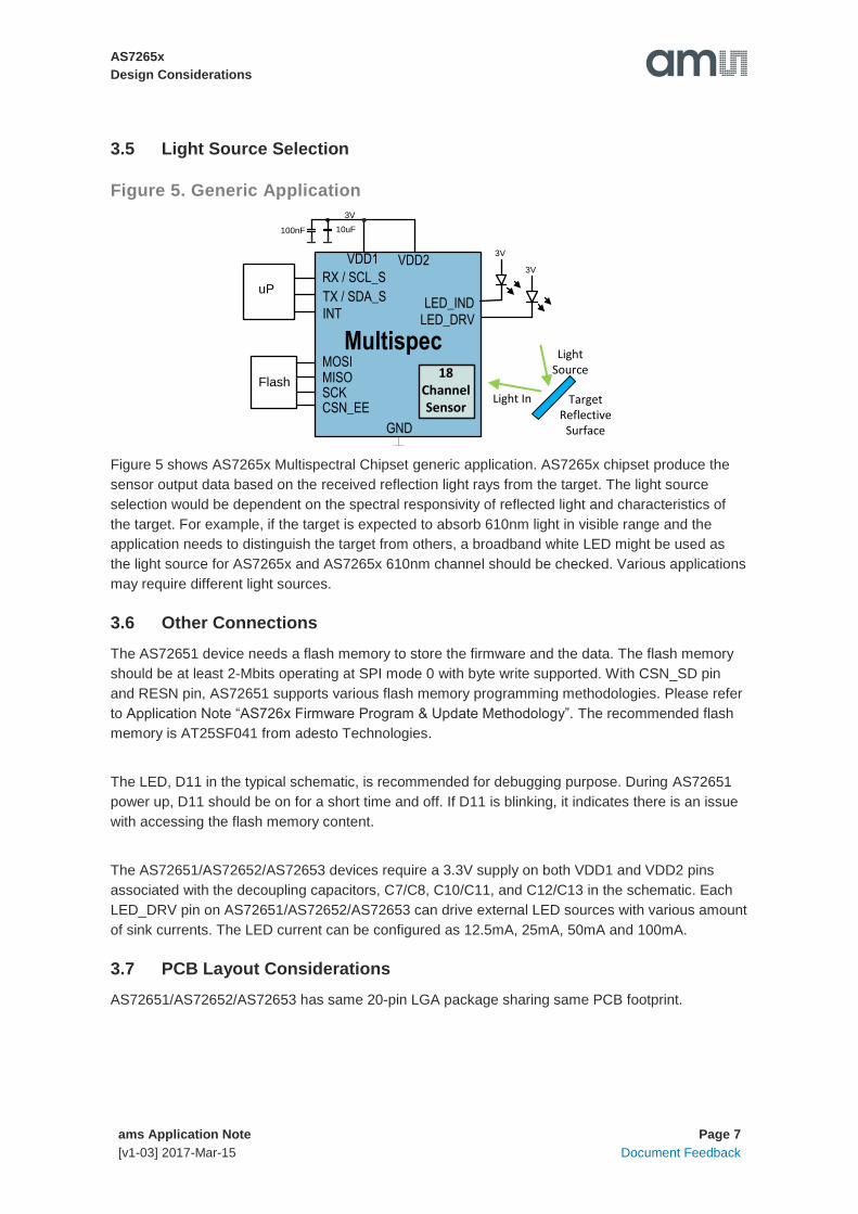
3.5 Light Source Selection
Figure 5. Generic Application
TargetReflective
Surface
100nF
RX / SCL_S
GND
LED_DRV
SCKCSN_EE
MISOMOSI
VDD1 VDD2
Multispec
uP
10uF
3V
3V
TX / SDA_S LED_IND
3V
Flash18
Channel Sensor
Light Source
Light In
INT
Figure 5 shows AS7265x Multispectral Chipset generic application. AS7265x chipset produce the
sensor output data based on the received reflection light rays from the target. The light source
selection would be dependent on the spectral responsivity of reflected light and characteristics of
the target. For example, if the target is expected to absorb 610nm light in visible range and the
application needs to distinguish the target from others, a broadband white LED might be used as
the light source for AS7265x and AS7265x 610nm channel should be checked. Various applications
may require different light sources.
3.6 Other Connections
The AS72651 device needs a flash memory to store the firmware and the data. The flash memory
should be at least 2-Mbits operating at SPI mode 0 with byte write supported. With CSN_SD pin
and RESN pin, AS72651 supports various flash memory programming methodologies. Please refer
to Application Note “AS726x Firmware Program & Update Methodology”. The recommended flash
memory is AT25SF041 from adesto Technologies.
The LED, D11 in the typical schematic, is recommended for debugging purpose. During AS72651
power up, D11 should be on for a short time and off. If D11 is blinking, it indicates there is an issue
with accessing the flash memory content.
The AS72651/AS72652/AS72653 devices require a 3.3V supply on both VDD1 and VDD2 pins
associated with the decoupling capacitors, C7/C8, C10/C11, and C12/C13 in the schematic. Each
LED_DRV pin on AS72651/AS72652/AS72653 can drive external LED sources with various amount
of sink currents. The LED current can be configured as 12.5mA, 25mA, 50mA and 100mA.
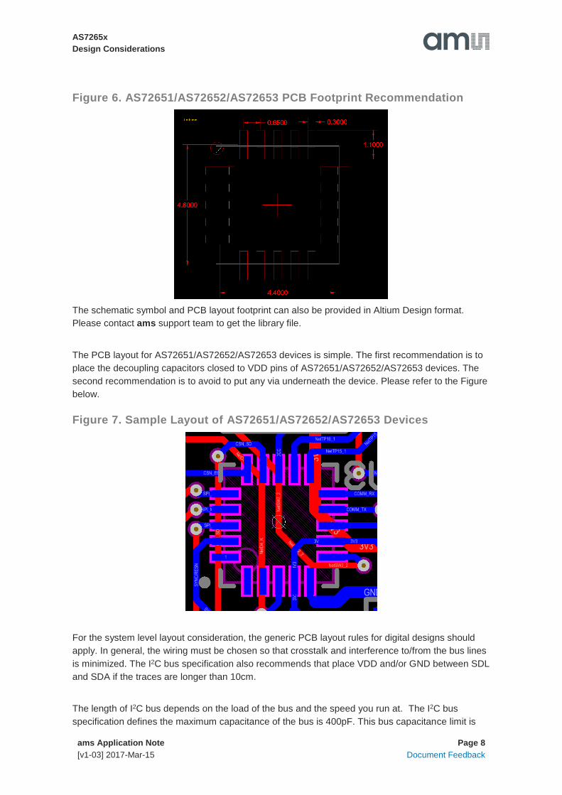
3.7 PCB Layout Considerations
AS72651/AS72652/AS72653 has same 20-pin LGA package sharing same PCB footprint.
AS7265x
Design Considerations
ams Application Note Page 8
[v1-03] 2017-Mar-15 Document Feedback
Figure 6. AS72651/AS72652/AS72653 PCB Footprint Recommendation
The schematic symbol and PCB layout footprint can also be provided in Altium Design format.
Please contact ams support team to get the library file.
The PCB layout for AS72651/AS72652/AS72653 devices is simple. The first recommendation is to
place the decoupling capacitors closed to VDD pins of AS72651/AS72652/AS72653 devices. The
second recommendation is to avoid to put any via underneath the device. Please refer to the Figure
below.
Figure 7. Sample Layout of AS72651/AS72652/AS72653 Devices
For the system level layout consideration, the generic PCB layout rules for digital designs should
apply. In general, the wiring must be chosen so that crosstalk and interference to/from the bus lines
is minimized. The I2C bus specification also recommends that place VDD and/or GND between SDL
and SDA if the traces are longer than 10cm.
The length of I2C bus depends on the load of the bus and the speed you run at. The I2C bus
specification defines the maximum capacitance of the bus is 400pF. This bus capacitance limit is

AS7265x
Design Considerations
ams Application Note Page 9
[v1-03] 2017-Mar-15 Document Feedback
specified to limit rise time reductions and allow operating at the rated frequency. In general, with
lower frequency and/or lower capacitance of the bus, you can have longer bus length.
For most of I2C bus designs, the capacitance limit should be not the problem at all. If you design
involves some unusual conditions, the specification has several strategies to cope with excess bus
capacitance. For example, higher drive outputs, bus buffers, switched pull-up circuit etc. Please
refer to the specification Section 7.2.
3.8 Optic Considerations
Figure 8. Aperture
Each AS7265x device has an open aperture on the surface. The diameter is 0.75mm and the
package field of view is ±20.5°. The light rays in the range as shown in above figure would arrive at
the sensor.
Since AS7265x Multispectral Chipset consists of three AS7265x devices, an external optical device
might be needed so incident rays to each device is same.
As an open-aperture device, precautions must be taken to avoid particulate or solvent
contamination as a result of any manufacturing processes, including pick and place, reflow,
cleaning, integration assembly and/or testing.
4 Software Design Considerations
In most of system designs, AS72651 is controlled by a microcontroller. With the UART interface, the
controller could configure the devices and get the sensors data through some AT commands. The
software of microcontroller design would be simple.
The following sections would focus on I2C interface and the software of microcontroller design
should satisfy both I2C specification and AS7265x Multispectral Chipset register structure.
4.1 Features and Register Structure
AS72651 supports I2C both standard mode and fast mode. The addressing mode is 7+1-bit so
when the controller send a read command to AS72651, the salve address plus R/W bit should be
0x93 and when sending a write command, it should be 0x92. Both read and write are single byte
process.
AS72651 does not support the slave clock stretching mode.
DIE
Lens
Sensor
2.5mm
0.75mm
20.5°
12°
Input Light Rays Range

AS7265x
Design Considerations
ams Application Note Page 10
[v1-03] 2017-Mar-15 Document Feedback
AS72651 has only three hardware based registers, STATUS (0x00), WRITE (0x01), and READ
(0x02). The rest are implemented as virtual registers in the firmware. All virtual registers are
accessed through WRITE and/or READ registers. Please refer to the data sheets for complete set
of virtual registers.
4.2 I2C Virtual Register Read
To read an I2C virtual register, please follow the flow chart below.
Figure 9. Flow Chart for Virtual Register Read
Write the Virtual Reg AddrI2C.Write Reg=0x01 Data=0xXXNote: 0xXX is the virtual register address
Read STATUSI2C.Read Reg=0x00
Read the dataI2C.Read Reg=0x02
Yes
TX_VALID bit = 1?
No
Read STATUSI2C.Read Reg=0x00
RX_VALID bit = 1?
Yes
No
To poll the STATUS register, the controller should write the STATUS address then following a read
command to get the value of the STATUS register. The Figure 3 shows the format of the command
for polling the STATUS register.
Figure 10. Command for Polling the STATUS Register
Start 0x92 STATUS Ack Repeat Start 0x93 Data Nack Stop
To write the virtual register address, please program WRITE register with the virtual register
address as the following format.
Figure 11. Command for Writing the Virtual Register Address for Reading
Start 0x92 WRITE Ack Virtual Reg Addr Ack Stop
Finally below is the reading command to get the data.
Figure 12. Command for Reading the READ register
Start 0x92 READ Ack Repeat Start 0x93 Data Nack Stop
AS7265x
Design Considerations
ams Application Note Page 11
[v1-03] 2017-Mar-15 Document Feedback
Figure 13. Sample Code of Reading a Virtual Register
#define I2C_AS72XX_SLAVE_STATUS_REG 0x00
#define I2C_AS72XX_SLAVE_WRITE_REG 0x01
#define I2C_AS72XX_SLAVE_READ_REG 0x02
#define I2C_AS72XX_SLAVE_TX_VALID 0x02
#define I2C_AS72XX_SLAVE_RX_VALID 0x01
uint8_t i2cm_AS72xx_read(uint8_t virtualReg)
{
volatile uint8_t status, d ;
while (1)
{
// Read slave I2C status to see if we can write the reg address.
status = i2cm_read(I2C_AS72XX_SLAVE_STATUS_REG) ;
if ((status & I2C_AS72XX_SLAVE_TX_VALID) == 0)
// No inbound TX pending at slave. Okay to write now.
break ;
}
// Send the virtual register address
i2cm_write(I2C_AS72XX_SLAVE_WRITE_REG, virtualReg) ;
while (1)
{
// Read the slave I2C status to see if our read data is available.
status = i2cm_read(I2C_AS72XX_SLAVE_STATUS_REG) ;
if ((status & I2C_AS72XX_SLAVE_RX_VALID) != 0)
// Read data is ready for us.
break ;
}
// Read the data to complete the operation.
d = i2cm_read(I2C_AS72XX_SLAVE_READ_REG) ;
return d ;
}
4.3 I2C Virtual Register Write
Writing to a virtual register is similar to the read.

AS7265x
Design Considerations
ams Application Note Page 12
[v1-03] 2017-Mar-15 Document Feedback
Figure 14. Flow Chart for Virtual Register Write
Write the Virtual Reg AddrI2C.Write Reg=0x01 Data=0xXX|0x80
Note: 0xXX is the virtual register address
Read STATUSI2C.Read Reg=0x00
Write the dataI2C.Write Reg=0x01 Data=0xXX
Note: 0xXX is the data
No
TX_VALID bit = 1?
No
Read STATUSI2C.Read Reg=0x00
TX_VALID bit = 1?
Yes
Yes
Please refer to the previous section for polling the STATUS register.
Writing the virtual register address for writing is not same as the one for reading. The MSB of the
virtual register address has to be set to 1 for writing.
Figure 15. Command for Writing the Virtual Register Address for Writing
Start 0x92 WRITE Ack Virtual Reg Addr | 0x80 Ack Stop
Simple command for writing the data as below.
Figure 16. Command for Writing the Data
Start 0x92 WRITE Ack Data Ack Stop
Figure 17. Sample Code of Writing a Virtual Register
void i2cm_AS72xx_write(uint8_t virtualReg, uint8_t d)
{
volatile uint8_t status;
while (1)
{
// Read slave I2C status to see if we can write the reg address.
status = i2cm_read(I2C_AS72XX_SLAVE_STATUS_REG);
if ((status & I2C_AS72XX_SLAVE_TX_VALID) == 0)

AS7265x
Design Considerations
ams Application Note Page 13
[v1-03] 2017-Mar-15 Document Feedback
// No inbound TX pending at slave. Okay to write now.
break ;
}
// Send the virtual register address
// (setting bit 7 to indicate a pending write).
i2cm_write(I2C_AS72XX_SLAVE_WRITE_REG, (virtualReg | 0x80)) ;
while (1)
{
// Read the slave I2C status to see if we can write the data byte.
status = i2cm_read(I2C_AS72XX_SLAVE_STATUS_REG) ;
if ((status & I2C_AS72XX_SLAVE_TX_VALID) == 0)
// No inbound TX pending at slave. Okay to write data now.
break ;
}
// Send the data to complete the operation.
i2cm_write(I2C_AS72XX_SLAVE_WRITE_REG, d) ;
}

AS7265x
Design Considerations
ams Application Note Page 14
[v1-03] 2017-Mar-15 Document Feedback
5 Contact Information
Buy our products or get free samples online at:
www.ams.com/ICdirect
Technical Support is available at:
www.ams.com/Technical-Support
Provide feedback about this document at:
www.ams.com/Document-Feedback
For further information and requests, e-mail us at:
For sales offices, distributors and representatives, please visit:
www.ams.com/contact
Headquarters
ams AG
Tobelbader Strasse 30
8141 Premstaetten
Austria, Europe
Tel: +43 (0) 3136 500 0
Website: www.ams.com

AS7265x
Design Considerations
ams Application Note Page 15
[v1-03] 2017-Mar-15 Document Feedback
6 Copyrights & Disclaimer
Copyright ams AG, Tobelbader Strasse 30, 8141 Premstaetten, Austria-Europe. Trademarks
Registered. All rights reserved. The material herein may not be reproduced, adapted, merged,
translated, stored, or used without the prior written consent of the copyright owner.
Information in this document is believed to be accurate and reliable. However, ams AG does not
give any representations or warranties, expressed or implied, as to the accuracy or completeness of
such information and shall have no liability for the consequences of use of such information.
Applications that are described herein are for illustrative purposes only. ams AG makes no
representation or warranty that such applications will be appropriate for the specified use without
further testing or modification. ams AG takes no responsibility for the design, operation and testing
of the applications and end-products as well as assistance with the applications or end-product
designs when using ams AG products. ams AG is not liable for the suitability and fit of ams AG
products in applications and end-products planned.
ams AG shall not be liable to recipient or any third party for any damages, including but not limited
to personal injury, property damage, loss of profits, loss of use, interruption of business or indirect,
special, incidental or consequential damages, of any kind, in connection with or arising out of the
furnishing, performance or use of the technical data or applications described herein. No obligation
or liability to recipient or any third party shall arise or flow out of ams AG rendering of technical or
other services.
ams AG reserves the right to change information in this document at any time and without notice.

AS7265x
Design Considerations
ams Application Note Page 16
[v1-03] 2017-Mar-15 Document Feedback
7 Revision Information
Changes from previous version to current revision 1-03 (2017-Mar-15) Page
Updated Figure 2 4
Added Light Source Selection and Optic Considerations 7, 9
Note: Page numbers for the previous version may differ from page numbers in the current revision.
Correction of typographical errors is not explicitly mentioned.