as good as gold and better: conducting metal oxide
TRANSCRIPT

As Good as Gold and Better: Conducting metal oxide
materials for mid-infrared plasmonic applications
Journal: Journal of Materials Chemistry C
Manuscript ID TC-REV-12-2017-005760.R1
Article Type: Review Article
Date Submitted by the Author: 30-Jun-2018
Complete List of Authors: Khamh, Hniang; North Carolina State University, Chemistry Sachet, Edward; North Carolina State University, Materials Science and Engineering Kelley, Kyle; North Carolina State University, Materials Science and Engineering Maria, J. P.; North Carolina State University, Materials
Franzen, Stefan; North Carolina State University, Chemistry
Journal of Materials Chemistry C
1
As Good as Gold and Better:
Conducting metal oxide materials for mid-infrared plasmonic applications
Hniang Khamh1, Edward Sachet
2, Kyle Kelly
2, Jon-Paul Maria
2, Stefan Franzen
1
1. Department of Chemistry, North Carolina State University, Raleigh, NC 27695
2. Department of Materials Science and Engineering, North Carolina State University,
Raleigh, NC 27695
Page 1 of 41 Journal of Materials Chemistry C

2
Abstract
The field of infrared surface plasmon resonance (IR-SPR) spectroscopy has the potential to
enable unique applications and technologies in chemical sensing, heat harvesting, and infrared
detectors. Finding an ideal material that can support a surface plasmon in the IR region has been
a challenge for more than a decade. High carrier mobility, > 200 ,and tunable carrier
concentration in the range 1019
< n < 1021
cm-3
are two necessary criteria for a spectrally narrow
tunable plasmon resonance band in the IR. The ideal material would also be easy to prepare and
robust in water and under ambient conditions. In this review, we highlight the development of
the field over the last decade. We also provide a guide to explain the extension of visible
plasmonics to the infrared region and the evolution of IR-SPR using conducting metal oxides
(CMOs). CMOs are free electron conductors and most of them have no interfering electronic or
vibrational transitions in the range of interest. Therefore, these materials also provide an
excellent test of the fundamental physics of SPR, including the effects of surface fields,
enhancement phenomena and the relationship between thin film epsilon near zero (ENZ) mode
and the localized surface plasmon resonance (LSPR) in nanocrystals. In summary, we discuss the
materials challenges and prospects for this field of research.
Page 2 of 41Journal of Materials Chemistry C

3
1. Introduction
Since the emergence of the field of surface plasmon resonance (SPR) spectroscopy in the
1950’s, the SPR technique has been developed primarily employing the noble metals Au and Ag
because of the accessibility of resonances in the visible region of the electromagnetic spectrum in
these metals.1 The idea of extending the SPR phenomenon to new materials and to the infrared
(IR) region in the wavelength range from 1 to 10 microns has only been explored during the past
decade.2-4
Fundamentally, the physics of SPR does not change in the IR compared to the visible
region, but the materials requirements are dramatically different. The optical resonances in Au
and Ag can be tuned by changing the size and shape of colloids and nanoscale surface structures,
but the charge carrier density and mobility are fixed material properties in metals. As radiation is
tuned further from resonance with the bulk plasmon of Ag and Au, the losses in these materials
increase dramatically. Consequently, IR applications require new materials. The concept of a
tunable surface plasmon in a free electron conductor was introduced with the suggestion that
semiconductors can serve as tunable materials in the infrared region for SPR applications.5, 6
Research efforts in the past decade have shown that there are numerous conducting metal oxides
(CMOs) that have an appropriate carrier density to support SPR in the mid-IR region.6-8
However, the crucial property of a useful SPR material is a sufficiently large free carrier mobility
to permit a high quality factor, i.e. a narrow, sharp SPR band.9
For many years ITO has been the workhorse in the field of near-IR SPR spectroscopy. Using
indium tin oxide (ITO), it was possible to systematically determine the effect of material
parameters and thin film preparation on the SPR response.10, 11
Although ITO is a versatile
material for demonstrating the range of possible effects in the near-IR (from 1-2 microns), it is
far from the ideal SPR material for IR applications because of its low mobility (< 30 cm2/Vs).
ITO has typically high defect concentrations since the doping level of Sn is relatively high (ca.
10%) in standard thin film preparations. In practice, the SPR in ITO is much broader than in Au
and there appears to be no feasible way to produce a thin film of ITO with sufficiently high free
carrier mobility to overcome this limitation.10, 11
There are many CMOs to consider that may have a desirable combination of free carrier
density and mobility appropriate for mid-IR SPR applications. Doped ZnO has been investigated
because it is robust material, inexpensive and supports lower doping levels than ITO.5, 12-14
ZnO
Page 3 of 41 Journal of Materials Chemistry C

4
can be doped with Al, Ga or other ions at lower concentrations than tin in ITO to achieve
conducting thin films with free carrier densities appropriate for mid-IR applications. However,
the mobility of ZnO films is also low and the SPR is correspondingly broad. There have been a
few studies on other oxides, e.g. strontium ruthenate, which have similar limitations. The studies
of a variety of CMOs leads to the conclusion that the starting point for design of a new material
is to identify a CMO that has a high mobility. It has long been known that CdO has high
mobility, but the appropriate doped CMO films for mid-IR applications were not known until
recently.9
In 2015 dysprosium-doped cadmium oxide (CdO:Dy) was demonstrated as a gateway
material that can support narrow, high quality SPR in the mid-IR region.9 Based on this work, we
will address the interplay of theory and experiment involved in the extension of SPR from visible
to infrared region, theory of SPR technique, and the evolution of CMO materials that has been
developed for IR-SPR, and the future of IR-SPR using CMOs and their possible applications.
The development of SPR in thin film materials has been complemented by studies of localized
surface plasmon resonance (LSPR) in nanoparticles and nanostructures.15-17
While the
geometries differ, both SPR and LSPR depends on the inherent transport properties of a material
to support a surface plasmon polariton (SPP), which is a consequence of the natural resonant
frequency in the material due to free charge carriers. Electromagnetic radiation can drive a
resonance in the material, but that effect is dependent upon the angle of incidence in a thin film
(SPR) or the geometry of a nanostructure (LSPR), both of which affect the conservation of
momentum of the absorbed photons. The development of mid-IR LSPR in parallel to thin film
SPR provides complementary information on the materials and their possible applications. We
will give the theoretical and experimental background that has motivated the focus on CMOs as
the most promising materials for mid-IR plasmonic applications. Finally, we will discuss
connection between the epsilon-near-zero (ENZ) mode and the LSPR in our brief review of the
theoretical background of the observed optical properties of thin films and nanostructures in the
mid-IR.
1.1.The Drude Model for optical properties of Conducting Metal Oxides
A plasmon resonance that can be described using the free electron (Drude) model can be
called a “pure plasmon”. The Drude model was constructed to explain the transport properties of
Page 4 of 41Journal of Materials Chemistry C

5
conduction electrons in an ideal material. It has been applied to conductivity in metals,
conductive oxides and heavily doped semiconductors despite the fact that there is a significant
departure from ideal behavior in many of these materials. For example, the Drude model cannot
capture the optical effects of interband transitions of the noble metals, Au and Ag, in the visible
and near-IR. The model is applicable to most CMOs provided their bandgaps are sufficiently
high. The CMOs of interest are transparent in the visible region or colored reddish or orange
with band gaps range from 2-3 eV. The observed ENZ in these materials ranges from 0.2-1.0 eV.
The bandgap energy is significantly greater than the plasmon band energy in all of these
materials. Thus, the difference in energy between bandgap transitions and the optical resonances
due to plasmons is quite large. Provided there are no interband transitions, the Drude model
accurately describes the optical properties of a CMO based on the equation of motion of an
electron in a field of nuclei with three adjustable parameters. The dielectric function of a
conductor can be described using Drude model as follows:
= − = − (1.1)
The real and imaginary dielectric function can be separated as:
= − (1.2)
= (1.3)
The plasma frequency and damping constant can be described by:
= (1.4)
! = "##
(1.5)
dielectric function
high frequency limit
! damping constant
Page 5 of 41 Journal of Materials Chemistry C
6
plasma frequency
n carrier density
q electron charge
$ the permittivity of vacuum
%&'' effective electron mass
µ mobility
The first parameter is the charge carrier density, n. CMO carrier densities in the range of interest
for IR applications (1019
–1021
cm-3
) are two to four orders of magnitude lower than those of
noble metals (ca. 1023
cm-3
). As given in equation (1.3), the plasma frequency is proportional to
the square root of the carrier density. The free electron model has proven very accurate for
describing the mid- and near infrared portion of the spectrum, which covers the optical properties
of these semiconductors in the range from 1,000 – 10,000 cm-1
. The longer wavelengths used to
drive SPR in CMOs have consequences for the spatial extent of plasmonic fields as well as the
thickness of metal oxide thin films required for the effect to be observed.
The second phenomenological parameter in the Drude model is the damping, !. The damping
in plasmonic spectroscopy plays a similar role to the dephasing rate in optical spectroscopy. An
increase in damping results in a spectrally broader plasmon. This parameter turns out to be of
crucial interest for applications since the spectral bandwidth of the plasmonic resonance
determines its utility for nearly every application of interest. In metals there is no practical way
to tune the damping, but it is sufficiently low for the noble metals that useful SPR effects can be
observed in the UV-VIS. CMOs present a pronounced variability in ! owing to the two material
parameters that comprise the damping, the mobility () and the effective mass (%&''), whose
relationships are given in equation (1.5). Equation 1.3 shows that the loss ( ) is roughly
proportional to !. The effective mass is a property governed by the band structure of the CMO
and can be considered a material constant. The high frequency dielectric constant() is a
parameter that depends on the degree of screening of the lattice by the electron distribution in the
solid. The distribution is a property of the material and it is difficult to imagine that there will be
opportunities to significantly engineer this parameter.
Page 6 of 41Journal of Materials Chemistry C

7
The Drude model is a simple yet effective model that permits us to predict the dielectric
properties in the frequency band of interest for any CMO using only four material parameters:
carrier concentration, mobility, effective mass of the free carrier and high frequency dielectric
constant. Two of the material parameters simultaneously affect the phenomenological damping,
which reduces the number of parameters in the basic Drude theory to three. From the perspective
of material design, we will show that by far the most important two parameters are n and. n
controls the wave number of the surface plasmon band and is the material parameter that can
be engineered to enhance plasmonic performance by tuning the spectral bandwidth. One can
relate the mobility to the degree of scattering of electrons by the lattice and carrier screening.
Lattice defects, such as grain boundaries increase scattering and reduce performance.
A dielectric function of a generic Drude material with a given value for n, µ, %&''and
can be plotted as depicted in Figure 1. (solid) and (dashed) are the real and the imaginary
components of the dielectric function, respectively. decreases steadily as the energy decreases
while exhibits the opposite trend. As frequency is lowered the real part changes sign from
positive to negative at a frequency known as the epsilon-near-zero (ENZ) frequency, then falls
steeply below this value. The ENZ frequency is of interest in its own right because of the fact
that a thin film can absorb all of the energy in an incident electromagnetic wave at this
frequency.18-20
The region just below the ENZ frequency comprises the range of interest for IR-
SPR since plasmonic oscillation can only be supported if < 0. The imaginary component ,
also called the loss tangent, approaches zero at high frequency (1.3). increases as the
frequency is lowered with a hyperbolic frequency dependence becoming significant for energies
where becomes negative. Recognition of the nature of the requirements for observation of
SPR in terms of and defines the challenge for development of a robust material that can
support SPR in the infrared region in terms of material properties that can be controlled by
experimental conditions.
Page 7 of 41 Journal of Materials Chemistry C

8
Figure 1. Example plot of Drude model dielectric: The real part (solid) and the imaginary part
(dash) plotted as a function of energy.21
1.2.The effects of material property variables in the Drude model
The effect of four parameters, n,,%&'' and can be considered independently to fully
understand how the Drude model depends on material properties. We can further differentiate
between parameters that are dependent on the preparation conditions, which are n and, and
those that are dependent on chemical composition, which are %&'' and . Keeping this
distinction in mind, we will discuss the general considerations of all four parameters.
Page 8 of 41Journal of Materials Chemistry C
9
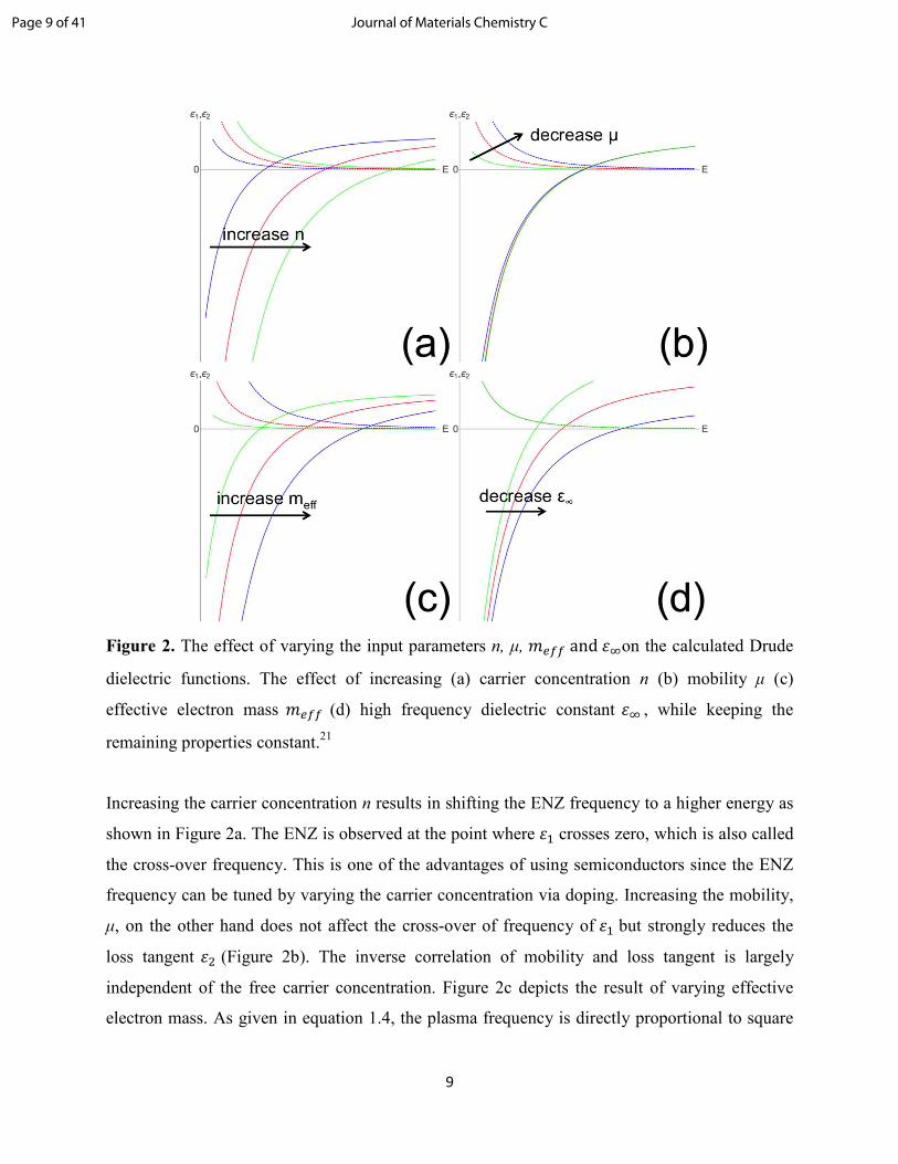
Figure 2. The effect of varying the input parameters n, µ, %&''andon the calculated Drude
dielectric functions. The effect of increasing (a) carrier concentration n (b) mobility µ (c)
effective electron mass %&'' (d) high frequency dielectric constant , while keeping the
remaining properties constant.21
Increasing the carrier concentration n results in shifting the ENZ frequency to a higher energy as
shown in Figure 2a. The ENZ is observed at the point where crosses zero, which is also called
the cross-over frequency. This is one of the advantages of using semiconductors since the ENZ
frequency can be tuned by varying the carrier concentration via doping. Increasing the mobility,
µ, on the other hand does not affect the cross-over of frequency of but strongly reduces the
loss tangent (Figure 2b). The inverse correlation of mobility and loss tangent is largely
independent of the free carrier concentration. Figure 2c depicts the result of varying effective
electron mass. As given in equation 1.4, the plasma frequency is directly proportional to square
Page 9 of 41 Journal of Materials Chemistry C

10
root of the ratio of the carrier concentration to the effective electron mass%&'' = -%&, where
%& is the electron mass and - is a screening parameter. The effect of decreasing effective mass is
to increase the carrier concentration; both the ENZ mode and the SPP shift to higher frequency
(wave number). Although a reduction in the effective mass increases the damping constant, !,
and correspondingly the loss function , this effect is not nearly as important as that of the
mobility. The range of %&'' values from 0.25%& < %&'' < 0.75%& is roughly a factor of three,
while mobility has a much greater range of values in practice 10 < < 5002%/45 spanning
at least a factor of 50. Of course, it crucial that %&'' is an inherent parameter that changes little
with film preparation, while can vary widely depending on sputtering and annealing
conditions. In general, we have shown that decreases as the lattice imperfections increase. 11
These imperfections may be caused by doping itself, which can disrupt the lattice or by
deposition conditions which affects the grain size and consequently the scattering length of
conduction electrons. Often there is an inverse relationship between n and since increasing the
density of free carriers by doping often increases the concentration of lattice imperfections due to
the mismatch in the radius of the dopant in relation to the original ion that was replaced.
However, we have also shown that the defect equilibrium is fixed in some materials due to
entropic effects, which means that compensating structural changes may occur that actually
reduce lattice imperfections caused by doping. The net effect of this fortuitous cancellation is
that n and can both increase over certain ranges.9 Although this effect has only recently been
discovered based on the work on CdO:M (M = Dy, Y, F), there is reason to believe that it is a
general effect in some classes of materials and may be important for the engineering of new
materials.
Finally, increasing the high frequency dielectric constant , shifts the ENZ frequency to a
higher energy without affecting the loss tangent. Increasingincreases the curvature of the
real part of the dielectric function, ε1, and consequently lowers the ENZ. Understanding the
effect of these input parameters for Drude model is essential in optimizing host materials for
plasmonic applications. Appropriate choice of host oxide materials permits one to obtain the
correct range for %&'' and . Selection of appropriate dopants, deposition and annealing
conditions permits control of n and to fine tune the optical properties. Appropriate experience
and understanding of the theory permits prediction of material properties in advance of film
Page 10 of 41Journal of Materials Chemistry C
11
preparation. The example of the correlation of n and due to the defect equilibrium also focuses
our attention on the fact that the parameters are not always independent. At present, these
correlations are sufficiently well understood to permit the design of tailor-made thin film
materials with SPR resonances in the mid-IR from 800 – 5000 cm-1
and sufficiently high
mobility for sensing and spectroscopic applications.
1.3. Experimental observation of the SPR phenomenon
In order to understand the various coupling schemes for surface plasmon resonance we
begin with the derivation from a model comprised of a thin metal film and a dielectric. In the
Drude model, it is assumed that motionless positive ions in the conductor are surrounded by a
non-interacting electron gas.22
As for the dielectric, a non-dispersive medium is assumed. This
section is based on a reduced form of the Drude model, which permits useful comparisons for
understanding the role of various parameters.21
In a lossless Drude metal given in eq 1.1, γ = 0.
Assuming = 1 and Ω = 6 , the lossless frequency dependent dielectric function (eq 1.1) can
be expressed as:
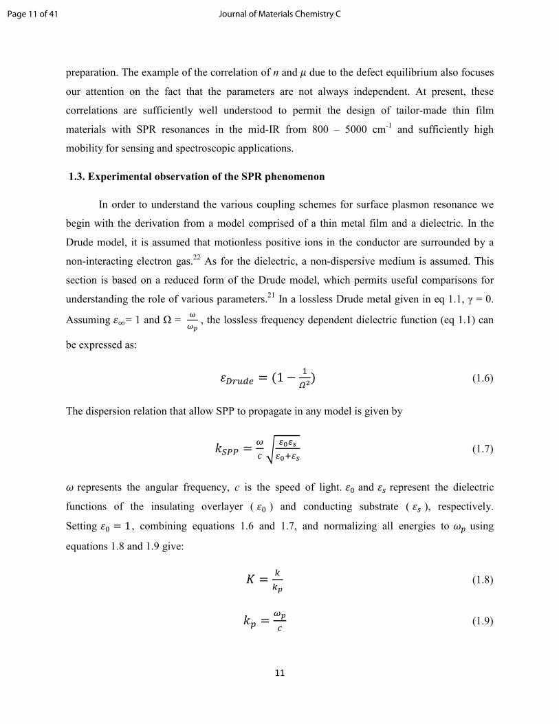
789:& = (1 − ;) (1.6)
The dispersion relation that allow SPP to propagate in any model is given by
<=>> = ?
? (1.7)
represents the angular frequency, c is the speed of light.$ and represent the dielectric
functions of the insulating overlayer ( $ ) and conducting substrate ( ), respectively.
Setting $ = 1 , combining equations 1.6 and 1.7, and normalizing all energies to using
equations 1.8 and 1.9 give:
@ = AA (1.8)
< = (1.9)
Page 11 of 41 Journal of Materials Chemistry C
12
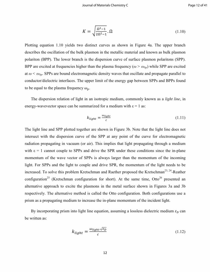
@ = BCBC . Ω (1.10)
Plotting equation 1.10 yields two distinct curves as shown in Figure 4a. The upper branch
describes the oscillation of the bulk plasmon in the metallic material and known as bulk plasmon
polariton (BPP). The lower branch is the dispersion curve of surface plasmon polaritons (SPP).
BPP are excited at frequencies higher than the plasma frequency (ω > ωbp) while SPP are excited
at ω < ωbp. SPPs are bound electromagnetic density waves that oscillate and propagate parallel to
conductor/dielectric interfaces. The upper limit of the energy gap between SPPs and BPPs found
to be equal to the plasma frequency.
The dispersion relation of light in an isotropic medium, commonly known as a light line, in
energy-wavevector space can be summarized for a medium with ε = 1 as:
<EFGH = IJKLM (1.11)
The light line and SPP plotted together are shown in Figure 3b. Note that the light line does not
intersect with the dispersion curve of the SPP at any point of the curve for electromagnetic
radiation propagating in vacuum (or air). This implies that light propagating through a medium
with ε = 1 cannot couple to SPPs and drive the SPR under these conditions since the in-plane
momentum of the wave vector of SPPs is always larger than the momentum of the incoming
light. For SPPs and the light to couple and drive SPR, the momentum of the light needs to be
increased. To solve this problem Kretschman and Raether proposed the Kretschman23, 24
-Reather
configuration25
(Kretschman configuration for short). At the same time, Otto26
presented an
alternative approach to excite the plasmons in the metal surface shown in Figures 3a and 3b
respectively. The alternative method is called the Otto configuration. Both configurations use a
prism as a propagating medium to increase the in-plane momentum of the incident light.
By incorporating prism into light line equation, assuming a lossless dielectric medium 7can
be written as:
<EFGH = IJKLM.√O (1.12)
Page 12 of 41Journal of Materials Chemistry C

13
Plotting this equation, one can see that the light line now intersects with the dispersion curve of
the SPP (Fig. 3c).
Figure 3. The dispersion curves as calculated using the Drude model and coupling of EM waves
with SPP. (a) the dispersive curve of BPP and SPP describe by Drude model in a metallic thin
film. (b) SPP dispersive curve with in a medium with epsilon = 1. (c) SPP dispersive curve
(a) (b)
(c)
Page 13 of 41 Journal of Materials Chemistry C

14
coupling to light by increasing the momentum of the incoming photons by using an optically
dense (ε > 1) prism.21
<(P)EFGH = IJKLM.√O.QRS(TJ) (1.13)
The total internal reflection method is used in both Kretschman and Otto configurations. The
incoming light kx propagates through the prism and an evanescent field is created by total
internal reflection. The coupling occurs when the momentum of this incoming light matches the
SPP dispersion. This phenomenon is known as surface plasmon resonance (SPR). In this
experiment, the in-plane wavevector of the incoming light can be varied by changing the angle of
the incoming light. If we include this angle variation of incident light, the modified equation is
given in eq 1.13. Plotting this equation for various angles with a SPPs dispersion indicates how
different angles give different resonance points (thus combinations of kx and energy) on the SPP
dispersion curve.
Figure 4. Schematic representation of how electromagnetic wave can couple with metallic thin
film via (a) Kretschman-Reather configuration. (b) Otto configuration.21
In both Kretschman and Otto configurations shown in Figure 4a and 4b the coupling
condition for SPR is met only by p-polarized light, since the angle of p-polarized light controls
the projection of the interfacial wavevector kx. At the proper angle the optically driven kx
matches the intrinsic kx of the SPP in the thin film. S-polarized light cannot couple to kx of the
(a) (b)
Page 14 of 41Journal of Materials Chemistry C

15
SPP in the thin film conductor. Under the coupling condition the incoming light energy of p-
polarized light is absorbed by the SPP. Experimentally, this can be observed as a drop in the
externally reflected light intensity, which is the essence of the SPR signal. The Kretschmann
configuration is usually used to excite surface plasmons while the Otto configuration is typically
used to excite bulk plasmons.
2. Materials for mid-infrared applications
Historically, SPPs have been investigated in noble metals: gold (Au) and silver (Ag). These
noble metals have played the dominant role in SPR development because their plasma
frequencies are in the visible region27-29
. Despite the fact that the plasma frequencies of most
metals are located in the deep ultraviolet30-32
, visible plasmons in Au and Ag are observed due to
the d-orbital contraction in the late transition metals, which leads to relativistic effects that lower
the energy of the d-band. 22
The net effect is that the Au and Ag plasmon resonance frequency
becomes coincident with the onset of band-to-band transitions with energies in the visible range.
However, this interband mixing also causes the plasmon bands of Au and Ag to have significant
losses due to absorption in the visible and near-UV.22, 33, 34
Although Au is known to be the more
lossy material compared to Ag in the visible region of the spectrum, it has been more widely
used because it is more inert and the plasma frequency is further to the red (8.89 eV32
), which is
more convenient for many experiments. It is evident from a study of the dielectric functions that
Au and Ag both have significant mixing of band-to-band transitions into the SPP. By contrast,
ITO does not have any such mixing.35
As mentioned previously, the ITO band gap is ca. 3.2 eV,
which is far higher in energy than the bulk plasma frequency, which corresponds to an energy of
1 eV. Consequently, the Drude free electron model is quite accurate as a description of ITO and
indeed other CMOs that have been studied. These facts are well known, but it is less appreciated
that because of the losses due to interband mixing neither Au nor Ag has a pure plasmon
polariton, defined as the SPP of a free electron conductor.
Although it is theoretically possible to induce the SPP of Au and Ag in the IR frequency
range, there are practical limitations.36, 37
While SPR has been observed in Au thin films in the
near-IR region, the Au loss function increases strongly as the frequency is lowered and there has
Page 15 of 41 Journal of Materials Chemistry C
16
been no similar demonstration of SPR in the mid-IR.38
The intraband loss is an inherent aspect of
any conductor, which arises from the imaginary part of the Drude model. Any conductor is
predicted by the theory to have an increase in loss below the plasma frequency.39
Therefore, it is
important to match the plasma frequency as closely as possible to the wavelength region of
interest. Other metals have even higher plasma frequencies and are even less suited for SPR in
the visible/IR than Au and Ag. These limitations led to a search for new materials supporting
SPPs in the mid-IR. These are mainly semi-conductors, doped Si, GaAs, InP, GaN, as well as
metal nitrides and oxides. Si and other (III-V) or (II-VI) semi-conductors have SPPs below the
mid-IR while the metal nitrides have SPPs above the mid-IR.40
Graphene is also an interesting
candidate, but like traditional semi-conductors it has a sufficiently small concentration of free
carriers to render it impractical for mid-IR applications. CMOs (ITO, Al:ZnO, Ga:ZnO, CdO:Dy,
F:SnO2, SrRuO2 and many others) have shown superior properties when compared to metal
nitrides.39-41
Thus, CMOs have dominated the field of mid-and near-IR plasmonics. Of these,
ITO has been the workhorse in most studies because of its wide availability due to its many
commercial applications. A key point in this review is that the successes of ITO as a breadboard
for laboratory study are overshadowed by limitations that make ITO a poor material for practical
applications. The field has focused on the fact that CMOs consist of a range of different doped
metal oxide materials that present possibilities for engineering of materials that have the desired
wavelength range and quality factor for practical applications.
2.1 Engineering CMO optical properties in the infrared region
The infrared region of the electromagnetic spectrum carries vibrational information about
chemical bonding and is widely used for detection of thermal contrast. There has been great
interest in investigating the optical properties of CMOs for their potential applications in
optoelectronic applications in the mid- and near-IR. Although there are only a handful of metal
oxides that are good candidates for the applications, the number of possible new materials is
nearly limitless when one considers the possible dopants, which are always an essential
ingredient in the design of CMOs. Thus, a substantial research effort has been devoted to finding
a robust material that can support SPP with low optical loss and tunability across the infrared
region. Beyond SPR there has been a great deal of interest in CMOs as metamaterials based on
the tuning of the ENZ in both thin films and nanostructures. Typical values of the ENZ mode are
Page 16 of 41Journal of Materials Chemistry C
17
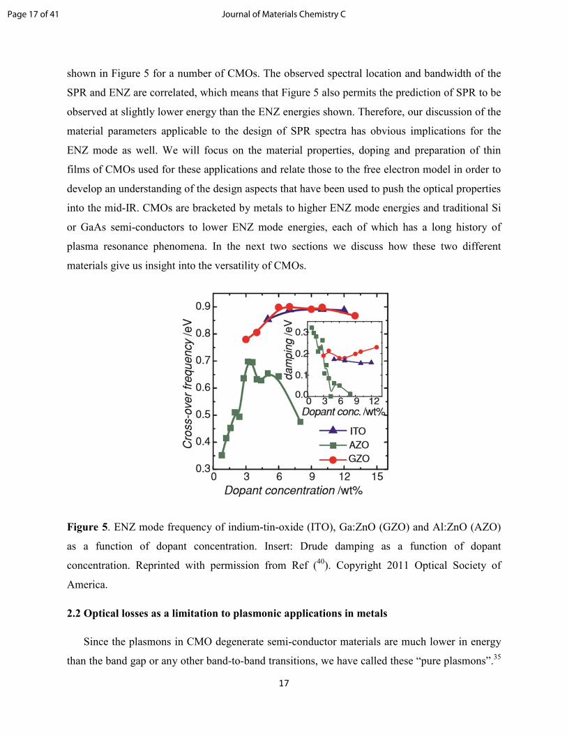
shown in Figure 5 for a number of CMOs. The observed spectral location and bandwidth of the
SPR and ENZ are correlated, which means that Figure 5 also permits the prediction of SPR to be
observed at slightly lower energy than the ENZ energies shown. Therefore, our discussion of the
material parameters applicable to the design of SPR spectra has obvious implications for the
ENZ mode as well. We will focus on the material properties, doping and preparation of thin
films of CMOs used for these applications and relate those to the free electron model in order to
develop an understanding of the design aspects that have been used to push the optical properties
into the mid-IR. CMOs are bracketed by metals to higher ENZ mode energies and traditional Si
or GaAs semi-conductors to lower ENZ mode energies, each of which has a long history of
plasma resonance phenomena. In the next two sections we discuss how these two different
materials give us insight into the versatility of CMOs.
Figure 5. ENZ mode frequency of indium-tin-oxide (ITO), Ga:ZnO (GZO) and Al:ZnO (AZO)
as a function of dopant concentration. Insert: Drude damping as a function of dopant
concentration. Reprinted with permission from Ref (40
). Copyright 2011 Optical Society of
America.
2.2 Optical losses as a limitation to plasmonic applications in metals
Since the plasmons in CMO degenerate semi-conductor materials are much lower in energy
than the band gap or any other band-to-band transitions, we have called these “pure plasmons”.35
Page 17 of 41 Journal of Materials Chemistry C

18
Figure 6 shows the contrast between the optical response of ITO and those of Au and Ag. Au has
absorption in the visible and UV above the plasma frequency, which is clearly observable as the
peaked feature in the red, imaginary part of the wave vector that is also associated with the loss
in the material. Au has significant increase in absorption or loss above the plasma frequency due
to interband transitions. Figure 6 also shows that Ag has a much smaller contribution from
interband transitions, which explains why Ag has been the choice for high quality plasmonic
material, despite its known disadvantage as a thin film material due to its high surface reactivity.
ITO was the first material investigated for its potential as a near-IR or mid-IR SPR material.6
The path to discovery of an infrared plasmonic material that possesses a high quality factor that
rivals Au or Ag in the visible involved consideration of a series of CMOs starting with ITO and
leading finally to the current highest quality factor observed in doped CdO.
The comparison of the dispersion curves in Figure 6 reveals a striking similarity between
ITO and Ag.35
The real response (blue) represents dispersion and plotted as ω vs. k to show the
dispersion of the material. The imaginary wave vector response (red) represents absorption of
light due to the ENZ. The peak of the absorption is coincident with the plasmon band gap. In
theory this is the mid-point between the top of the SPP and the starting point of the BPP (see
Figure 3). The dielectric curve of ITO was obtained from the Drude model based on the
measured values of n and , while Au and Ag were obtained from measured dielectric
functions. As shown in the Figure 6, the dispersion curve of ITO has a relative width and shape
that resembles the dispersion of Ag, although the wavenumber range for ITO is a factor of 4
lower than that of Ag. Ag has extinction to higher energy than the bulk plasma frequency, but
ITO has essentially no extinction on the high energy side of the bulk plasma frequency below the
bandgap (Figure 6A). Although Ag is considered the most suitable metal for plasmonic
applications based on its spectral features, ITO has a “purer” plasmon than Ag. Unlike Ag or
ITO, Au has a significant contribution from a d-to-p interband transition, which can be observed
in nanoparticle absorption spectra. This additional absorption at or above plasma frequency
shown in Figure 6B is not present in ITO and to a much smaller extent in Ag (Figure 6C).
Page 18 of 41Journal of Materials Chemistry C

19
Figure 6. The real (blue) and imaginary (red) response of wave vectors for (A) indium tin oxide
(ITO) (B) gold (Au) and (C) silver (Ag). Reprinted (adapted) with permission from (35
).
Copyright (2008) American Chemical Society
Although the noble metals are not tunable (i.e. in terms of their material properties), they can be
prepared as arrays or nanoparticles (nanostructures) that provide a seemingly limitless tunability
due to their shape.42
The LSPR of Au and Ag depends on the aspect ratio and aggregation state
of nanorods and nanoparticles.43, 44
The creation of ordered arrays of gold on patterned surfaces
has led to new ways to tune the LSPR of materials.45
These aspects of the noble metals are
currently being used as the pattern for similar experiments using CMOs.46
2.3 Far-IR SPR in indirect bandgap semi-conductors and graphene
The optical properties of doped silicon, which include its bulk plasma frequency, have been
known for decades.47-49
In addition, silicide materials have been studied more recently for
plasmonic optical properties.50, 51
The solid solubility, the upper limit of impurity concentration
that can be absorbed by the material, does not permit a sufficiently high dopant concentration to
reach the levels observed in many CMOs. Phosphorous has the highest solid solubility for
silicon at 1021
cm3. However, as the doping concentration approaches the solubility limit, the
doping efficiency decreases, which presents an intrinsic limitation to applications based on these
materials.52
In the final analysis, the free carrier concentrations in doped Si are so low that none
of silicon-based materials are suitable for mid-IR applications.
Page 19 of 41 Journal of Materials Chemistry C

20
Germanium is more promising for SPR applications because it has a higher electron mobility
than silicon53-55
. Germanium has a smaller optical bandgap than silicon and is typically doped
with gallium, aluminum and arsenic. Much like silicon, the solid solubility limit for dopants in
Ge do not permit high doping levels. Arsenides8, 56
, Phosphides57
and Nitrides40, 58
have also been
studied for infrared plasmonic applications. Although some of these materials have applications
in the far-IR, none of these materials are ideal materials for optical application in the mid-IR
region. The free carrier density of both doped Si and Ge limit the optical tuning range for the
plasmons of both Si and Ge semi-conductor materials to the far IR.
Graphene has attracted attention as a 2-D material that can support SPR and also may
have applications as a metamaterial.59-62
Graphene can support surface plasmons in the mid-IR
region, but only at low temperature (4.2K) because of high losses at room temperature. It is
worth noting that the limited data available indicate that CMOs have a modest temperature
dependence of both their band gaps and carrier densities.63
Similarly heavily doped Ge, which
has carrier densities in the same range as graphene shows a modest temperature dependence on
carrier density.54
Thus, the temperature dependence of SPR in graphene is an anomaly. As a
practical matter graphene has SPR resonance at wavelengths > 6.5 µm under ambient conditions,
which makes it most useful in the far-IR, the same region accessible to the plasmons of
traditional doped semi-conductors.64
2.4 Transparent Conducting Oxides as mid-IR and near-IR SPR Materials
In 2002, Franzen and Brewer hypothesized that pure plasmons can be observed in CMOs
based on the correlation of surface resistance a decrease of reflectivity in ITO in the near-IR
region.4, 65
Based on the understanding of the semi-conductor SPP, which was known at the time,
it was predicted that ITO would have the potential for SPR applications in sensing in the mid-
and near-IR analogous to Au in the visible. The prediction based on the reflectivity correlation
was observed in the detection of SPR in ITO in 2006 using a U − 2U stage attached to a Fourier
transform infrared (FTIR) spectrometer.66, 67
The optical response of ITO films was studied as a
function of thickness from 30 nm to 300 nm.11
Subsequently, the effect of thin film preparation
on the optical properties was quantified based on the Drude model.68
The use of hybrid Au:ITO
plasmonic thin films permitted a separation of the SPP and ENZ based on polarization.10
The
SPP can be excited by electromagnetic (EM) radiation aligned parallel to the interface of the thin
Page 20 of 41Journal of Materials Chemistry C

21
film and the ENZ can be excited only by EM radiation polarized perpendicular to the film
surface.10
While these studies demonstrated the utility of ITO as a material for theoretical study
of SPR in the near-IR the understanding derived from these studies led to the conclusion that the
quality factor of the SPR signal was approximately 5 times lower than that of Au because of the
low mobility of ITO (ca. 30 2% /Vs). Further experimental studies failed to find a feasible
preparation of a thin film of ITO with significantly higher mobility. Thus, these initial studies
revealed the need to investigate other CMOs focusing on maximizing the carrier mobility.
Attention was then focused on zinc oxides (ZnO). These metal oxides are also transparent to
visible light because of their large bandgap. Like ITO, doped-ZnOs are referred to as transparent
conducting oxides (TCOs). ZnO be doped degenerately to achieve conducting thin films that
possess metal like properties in the mid-IR and near-IR range. Conducting films, aluminum-
doped ZnO (AZO) 13, 69-71
, gallium-doped ZnO (GZO)12, 39, 69
were thoroughly investigated as
potential candidates for NIR applications. AZO thin films have lower losses with high doping,
but GZO and ITO have higher carrier concentrations.4, 72
Figure 3 depicts the carrier
concentration of the three materials as a function of doping concentration. While these materials
are tunable, easy to prepare and cheaper than ITO, they have the same disadvantage in that the
mobilities are quite low. None of the doped ZnO films studied to date has a quality factor that is
an improvement over ITO. The systematic study of ITO using the Drude model as a guide for
design led to an understanding of the role played by the mobility in the SPR of CMOs.
Ultimately, this process of measuring the optical response of various thin films pointed towards
to a new class of doped CdOs, which are the most promising materials to date for mid-IR SPR
applications.
2.5 Indium tin oxide as a testbed material for near-infrared plasmonic applications
ITO thin films are widely used in heat shielding materials73-75
and electrochemical
sensors76, 77
due to its optical properties being sensitive to small variations in their preparation
and annealing procedures. Hence, ITO is widely used as an infrared reflector and as transparent
electrode in the visible region.78-81
The observation that the ITO reflectance decreases in the
near-IR region proportional to the conductance of the respective thin film lead to the hypothesis
that ITO has potential as a plasmonic material in mid-IR region.4, 82
Using the Drude model, the
plasma frequency of ITO was predicted to occur in the near-IR region. Due to its band structure,
Page 21 of 41 Journal of Materials Chemistry C

22
ITO is an excellent material for direct observation of the optical properties within the
conducting, resonance and insulating regimes. The effects of the free electron theory have been
tested in ITO without interference from band-to-band transitions. The extinction in Ag and even
more so, those in Au (Figure 6B and 6C) arise from strong interband transitions, which deviate
significantly from the free electron model. While the Drude model has great predictive power for
ITO and other CMOs it has little utility in studies of the noble metals.
In the conducting regime, the electrons follow the incident electric field leading to
complete reflection in the absence of absorption losses (ω < ωp/√ = ωbp). ωbp is the frequency
of the bulk plasmon and is the high frequency dielectric constant. In the resonant regime, ω =
ωbp, one can excite the ENZ mode. When this was initially observed in very thin films of ITO,
we called this observation a capacitive plasmon resonance (CPR) to indicate that the field
excitation is perpendicular to the surface10
. This perpendicularly polarized resonance, which is
most commonly known today as the ENZ, has been known both from Abeles early work on
conducting films 83
and the analogous effect in insulating films, known as the Berreman mode.84,
85 The ENZ mode is only observed in thin films that are thinner than the skin depth of the
conductor. The ENZ mode has never been observed in Au or Ag because their skin depths are so
shallow (< 5 nm) and surface free energy is so high that it is essentially impossible to deposit a
film that is thinner than the skin depth. However, ITO has a skin depth of ~120 nm for films that
have ENZ modes in the near-IR. Mid-IR SPR materials such as CdO have skin depths > 200 nm
due to their lower carrier density. The ENZ mode is related the localized surface plasmon
resonance (LSPR) in a nanoparticle, although there will be a geometrical effect that shifts the
location of the resonance. Since the LSPR depends on particle size and shape the thin film value
of the analogous resonance is not precisely in the same region as the LSPR. One might think of
the thin film as a nanoparticle stretched out so that it forms a film. For example, in ITO the ENZ
mode (CPR) is observed at ~9,000 cm-1
10
in a 30 nm thick film. The ENZ mode in a hexagonal
geometric array of ITO triangular patterns with a thickness of 20 nm is observed at 6,200 cm-1
.46
The LSPR of ITO observed in nanoparticles at the same doping of 10% Sn is 6,200 cm-1
.86
While
it is difficult to know the exact carrier density in the nanoparticle the comparison underscores a
basic similarity between the wave number range of the ENZ and LSPR. Numerous experiments
on a variety of different CMOs show that the frequency of the ENZ mode and SPP are
correlated, and both are controlled by altering the charge carrier density.
Page 22 of 41Journal of Materials Chemistry C

23
Below the bulk plasma frequency ω < ωbp, light can couple into the material if it
propagates through an optically dense medium that permits total internal reflection at the
boundary. SPR can be observed by coupling light into a conducting layer such that there is a
propagating wave along the insulator-conductor interfaces on both sides of a conducting thin
film and an evanescent wave that penetrates into the conductor as shown in Figure 4. When light
propagates through vacuum or air, it is reflected for ω < ωbp. When ω > ωbp, ITO behaves
optically as an insulator and it is transparent in this regime. This observation underlines how
different the material interacts with EM waves dependent on their energy relative to the plasma
frequency. While these statements are true for any plasmonic material, they are much easier to
visualize in the CMOs. Despite its limitations for practical applications, ITO is still a useful
material for demonstrating the predictive utility of the free electron theory for engineering CMOs
as plasmonic materials.
2.6 Experimental considerations behind the first observation of SPR in ITO
The detection of SPR in a conducting metal oxide was first achieved using a FT-SPR
attachment for a FTIR spectrometer constructed by GWC Inc. (Madison, WI) in 2006.36, 37
ITO
has one of the highest charge carrier densities of any CMO, thus, it is well suited for
measurements in the near-IR range (5000 – 9000 cm-1
). The dependence of the SPR signal on the
thickness of the conducting film can be explained by referring to three thickness regimes.11
First, very thin ITO films of less than ~120 nm cannot support SPPs when used in Kretschmann
configuration because the phase shift in the evanescent field propagating through the cannot
match that of the incident radiation at any angle.
In order for incident light to couple into the SPP (see Figure 4) the conduction electrons
must oscillate in the vicinity of the conducting-insulator interface and result in an evanescent
field that decays exponentially, perpendicular to the interface, into the metal as well as the
dielectric. This decay has a limited penetration depth and known as skin depth. The skin depth is
related to the decay of the magnitude of the electric vector (E) 22
in ITO by
E = E0 exp (-t/δ) (2.1)
δ =
(VWX)Y/ (2.2)
Page 23 of 41 Journal of Materials Chemistry C

24
where t is the thickness of ITO, E0 is the original magnitude of the electric vector, c is the speed
of light and σ is the conductivity.
A film that is thinner than the skin depth of the conductor does not permit an electric
field oscillation along the conductor-insulator interface. This condition is present in panel 7A and
7B where the thicknesses are 30 nm and 55nm, respectively. There is no SPR signal and the
observed extinction is the ENZ mode in those panels. There is a transition between two regimes
shown in Figure 7C and 7D where multiple optical features are present. The optimal thickness
for ITO films is observed to be between 120-200 nm, which is shown in Figure 7E, 7F and 7G.
In this thickness range the phase shift induced by the loss tangent of the metal can match incident
radiation in the near-IR frequency range. In this thickness regime, ITO film can support SPP and
an angle-dependent SPR signal can be observed. The optimal thickness for the most common
ITO thin film preparation (10% Sn annealed in forming gas) is approximately 160 nm. In the
third regime when the film thickness increases beyond the optimal value the SPR signal
decreases in magnitude as shown in Figure 7H. As the thickness surpasses 200 nm the loss
tangent increases to the point where it is no longer possible to achieve a matching condition.
Viewed from another point of view the SPP is reduced proportional to the reduction in the
evanescent field at the second conductor-insulator interface. The SPR signal eventually vanishes
as is evidence in Figure 7I.
Page 24 of 41Journal of Materials Chemistry C

25
Figure 7. SPR spectra Rp/Rs obtained for ITO film thicknesses d from 30 (panel A) to 318 (panel
I). Each line represents an angle increment of 0.83. Used with permission from Ref (87
).
The SPP band is tunable with carrier concentration as depicted in Figure 8. The plasma
frequency shifted to lower energy as n decreases as depicted in eq (1.4). Although ITO was a
testbed material for infrared SPR, it has one major drawback. ITO has a low carrier mobility (30
cm2/Vs), which leads to a broad SPR response.
11 The width of the SPP band increases as the
mobility decreases as shown in Figure 9. This realization provides a systematic approach to
search for high mobility conducting metal oxides that can overcome this problem in the near and
mid-infrared region. The push to the mid-IR region is a pragmatic consideration since most
conducting metal oxides have charge carrier densities lower than ITO, which naturally places
them in the mid-IR region, which is also the region where molecular vibrations are observed by
FTIR spectroscopy.
Figure 8. The experimental and theoretical data for the carrier concentration series. The
corresponding charge carrier densities are given in each panel. Used with permission from Ref
(87
).
Page 25 of 41 Journal of Materials Chemistry C

26
Figure 9. The experimental data of mobility series, where the sputtering pressure of the target
gas is 9 mTorr for (a), 12 mTorr for (b), and 15 mTorr for (c). The corresponding mobilities are
given in each panel. Used with permission from Ref (87
).
ITO has been widely used in a variety of mid-IR plasmonic applications. The tuning of
plasmons in ITO is possible using carrier accumulation to modify the carrier density, which in
turn affects and the observed SPR reflectance minimum. 88
A large non-linear optical signal
was observed near the ENZ mode of ITO using ultrafast spectroscopy. 41
Switching of the ENZ
using ITO in a waveguide sandwiched between two Au electrodes has also been demonstrated.
Each of these applications shows how externally applied electric and optical field fields can be
used for photonic switching in CMO-based plasmonic materials. ITO is still the most useful
CMO for general demonstration of the possible photonic applications. But, materials in the mid-
IR with higher quality factors may ultimately provide the most interesting for end user
applications that involve heat measurement and capture, IR detectors, molecular sensing,
nanoscale spectroscopy, and optical circuits.
2.7 The Search for Appropriate Conducting Metal Oxides for mid-IR Applications
Once SPR in the near-IR region was established by the experimental observations in
ITO, the quest for new CMO materials with high mobility began in earnest. Most CMOs have
carrier densities lower than those of ITO so that the majority will have SPR in the mid-IR.
Page 26 of 41Journal of Materials Chemistry C
27
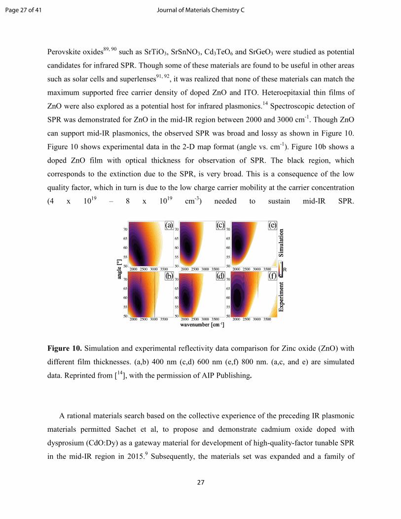
Perovskite oxides89, 90
such as SrTiO3, SrSnNO3, Cd3TeO6 and SrGeO3 were studied as potential
candidates for infrared SPR. Though some of these materials are found to be useful in other areas
such as solar cells and superlenses91, 92
, it was realized that none of these materials can match the
maximum supported free carrier density of doped ZnO and ITO. Heteroepitaxial thin films of
ZnO were also explored as a potential host for infrared plasmonics.14
Spectroscopic detection of
SPR was demonstrated for ZnO in the mid-IR region between 2000 and 3000 cm-1
. Though ZnO
can support mid-IR plasmonics, the observed SPR was broad and lossy as shown in Figure 10.
Figure 10 shows experimental data in the 2-D map format (angle vs. cm-1
). Figure 10b shows a
doped ZnO film with optical thickness for observation of SPR. The black region, which
corresponds to the extinction due to the SPR, is very broad. This is a consequence of the low
quality factor, which in turn is due to the low charge carrier mobility at the carrier concentration
(4 x 10¹⁹
– 8 x 10¹⁹
cm-3
) needed to sustain mid-IR SPR.
Figure 10. Simulation and experimental reflectivity data comparison for Zinc oxide (ZnO) with
different film thicknesses. (a,b) 400 nm (c,d) 600 nm (e,f) 800 nm. (a,c, and e) are simulated
data. Reprinted from [14
], with the permission of AIP Publishing.
A rational materials search based on the collective experience of the preceding IR plasmonic
materials permitted Sachet et al, to propose and demonstrate cadmium oxide doped with
dysprosium (CdO:Dy) as a gateway material for development of high-quality-factor tunable SPR
in the mid-IR region in 2015.9 Subsequently, the materials set was expanded and a family of
Page 27 of 41 Journal of Materials Chemistry C
28
doped CdO:M (M = Dy, Y, F etc.) exhibits sufficiently high mobility to support SPR at mid-IR
energies with low optical losses.
2.8 CdO:Dy: A Gateway Material for Mid-IR SPR
In 1969, the material properties of an intrinsic single crystalline CdO were reported by
Koffeyberg.93
According to the data in Ref. 89, single crystal CdO exhibits both mobilities and
carrier densities needed to support high quality mid-IR SPR. Simulations of the predicted optical
response for CdO in the mid-IR were conducted using the Fresnel equations combined with the
free electron model to approximate the CMO dielectric function. Subsequently, a thin film
growth method was developed using dysprosium (Dy) as a dopant. CdO doped with Dy
(CdO:Dy) thin film was observed to have low loss in the mid-IR due to its unusually high
mobility9 at carrier concentrations >10
19 cm
-3. The observed electron mobility was achieved
through defect equilibrium engineering of the CdO native and extrinsic crystallographic defects.
Although there are numerous candidate dopants that one can consider for CdO, Dy was the first
dopant used to successfully demonstrate this effect.
CdO is an intrinsic n-type semiconductor where free electrons originate from doubly
ionized O-vacancies (equation 3.12). By doping CdO with Dy, Dy populates the Cd sublattice
with 3+ charge and acts as extrinsic donor (equation 3.13). The defect equilibrium system of
intrinsic and extrinsic defect reactions is given as:
Cd[\] + O] ⟺ Cd[\] + V•• + 2d + O (2.3)
DyOghij⟹ 2Dy[\• + 2O] + 2d + O (2.4)
Although dysprosium on a Cd-site and an oxygen vacancy are both electron donors, Dy
substitution gives rise to a smaller lattice perturbation than an oxygen vacancy. The lattice
disruption of Dy doping is small because Cd and Dy have similar ionic radii ( r[\ =0.95nm, ropg = 0.92nm). 94
The singly charged n-type donor, Dy[\• in eqn. 2.4, increases at the
expense of the doubly charged n-type vacancy, V•• in eqn. 2.3 and the net effect of this
replacement is a decrease in lattice strain and a concomitant increase in mobility in parallel with
the increase in charge carrier density over a range of dopant concentration. Because impurity
scattering scales with Z2, there is less net scattering for 2n donors of charge e than n donors of
Page 28 of 41Journal of Materials Chemistry C
29
charge 2e at the same carrier density. These phenomena lead to the observed increase in mobility
up to a threshold charge carrier density above which the defect equilibrium is weighted towards
Dy[\• and the scattering from Dy begins to dominate. These competing effects define the useful
range of free carrier concentration within CdO that gives rise to a tunable, narrow bandwidth
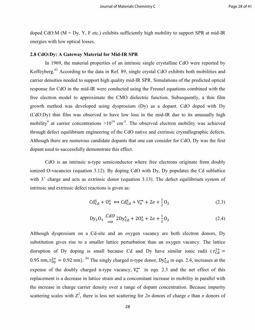
plasma resonance in the mid-IR region. The transport properties of CdO:Dy at room temperature
are presented in Figure 11. The conductivity and carrier concentration are both observed to
increase as Dy doping concentration increases spanning the range of 5 x10¹⁹
– 1 x10²¹
cm-3
.
Mobility follows the same trend until it reaches its maximum mobility value of 500 cm2V
-1s
-1 at
5 x 10¹⁹
cm-3
. Beyond this Dy concentration, carrier mobility decreases until the limit of 5 x 10²¹
cm-3
. This unique combination of high carrier density and mobility of CdO:Dy makes it an ideal
plasmonic host at mid-IR frequencies.
Figure 11. Transport properties of CdO:Dy carrier concentration (n), carrier mobility (µ) and
conductivity (σ) as a function of Dy concentration. Reprinted by permission from Macmillan
Publishers Ltd: Ref [9], copyright (2015)
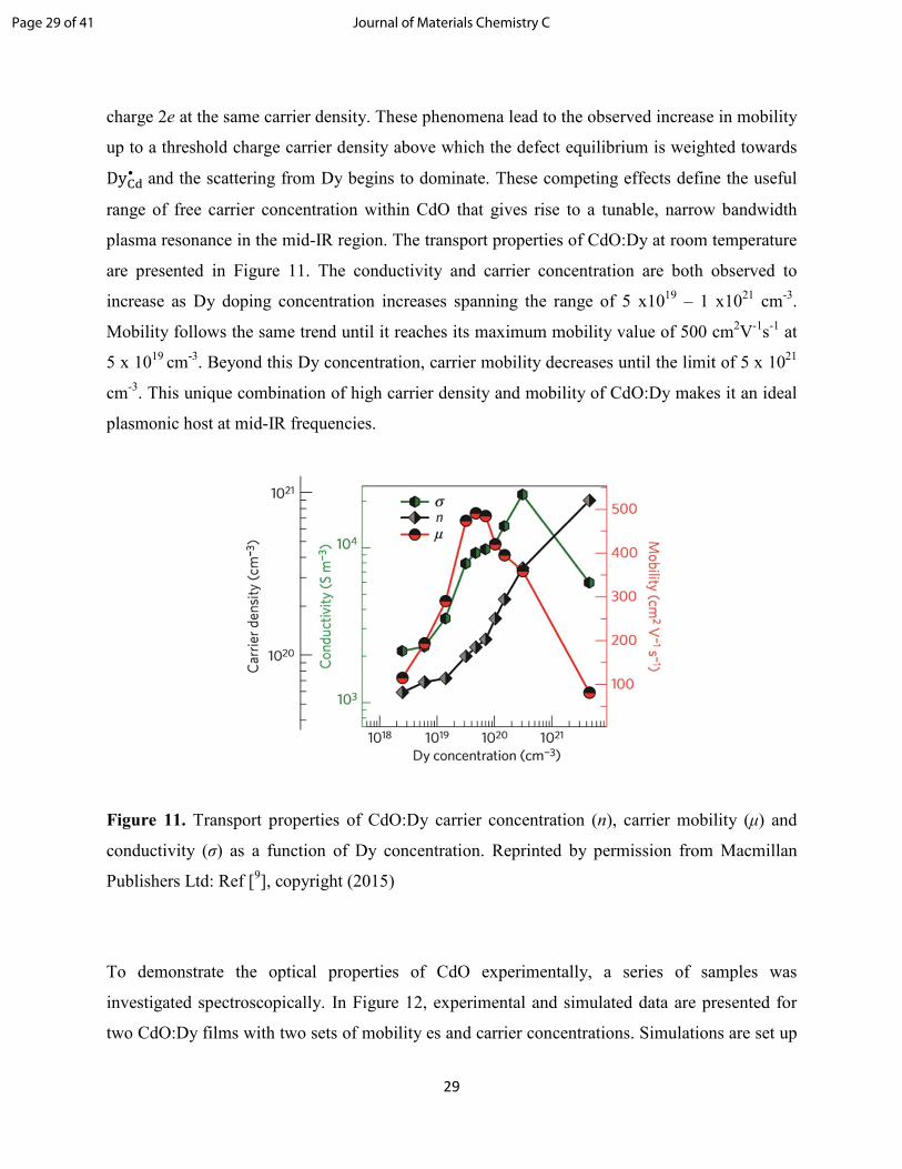
To demonstrate the optical properties of CdO experimentally, a series of samples was
investigated spectroscopically. In Figure 12, experimental and simulated data are presented for
two CdO:Dy films with two sets of mobility es and carrier concentrations. Simulations are set up
Page 29 of 41 Journal of Materials Chemistry C
30
to optimize the ideal condition for the substrate by incorporating all optical components of the
experiment. The SPR data were recorded in the Kretschmann configuration using a Woollam®
IR-Variable Angle Spectroscopic Ellipsometer (VASE). As mentioned for ITO in section 2.4, the
phase shift has to be accounted for experimentally by varying the thickness of the CdO thin
films. Extremely smooth CdO:Dy substrates presented in Figure 12 were grown using an oxide
molecular beam epitaxy (MBE) environment. Figure 12b shows the experimentally determined
SPR dispersion curve as the black curve. The black color indicates extinction due to plasmonic
resonances. The relatively narrow feature of this curve is an indication of a high quality factor,
which is attributable to the high mobility of 478 cm2/Vs. The reader should compare this 2-D
plot to that of Al:ZnO in Figure 10b. The SPR dispersion feature in the 2-D of Al:ZnO should be
curved in the same way as the one is in Figure 12b. However, the feature is so broad in Figure
10b that is not possible to discern its shape. Figure 12d shows a thin film that has a significantly
high free carrier density (3.3 x 10²⁰
cm3 in Figure 12d compared to 1.3 x 10
20 cm
3 in Figure 12b).
As a consequence, the ENZ is shifted 3,500 cm-1
in Figure 12b to a value greater than 3,800 cm-1
(i.e. it is no longer visible on the plot of Figure 12d because it is shifted to an energy to the right
of the plot limit).
Figure 12. Simulated reflectivity data and experimental data of CdO:Dy with thickness of 520 and 280
nm by varying mobility and carrier density. Reprinted by permission from Macmillan Publishers
Ltd: Ref [9], copyright (2015)
2.9 Further advances in CdO:M doping (M = Dy, Y, F) and in thin film preparation
Page 30 of 41Journal of Materials Chemistry C
31
Highly accurate doping using MBE was the key to investigate the structure property
relations in CdO:Dy. However, the limited throughput and high cost of MBE present a barrier to
larger scale application of this material. Recently, thin films have been prepared using several
other dopants by RF-assisted reactive High-Power Impulse Magnetron Sputtering (or HiPIMS).
95, 96 These dopants include yttrium and fluorine, among several others. Notably, CdO:Y grown
via HiPIMS demonstrates mobility in excess of 400 cm2V
-1s
-1 with a carrier density of ~10
20 cm
-
3. For films grown on sapphire, these results are superior to those achieved using MBE.
Furthermore, it has been demonstrated that the carrier density can be reproducibly tuned between
low 1019
and mid 1020
carrier concentrations by controlling the magnetron power and the cathode
to substrate distance for the dopant source. With dopants such as dysprosium, yttrium and
fluorine in conjunction with multiple deposition methods, one can engineer doped CdO with
tailored properties suitable for a variety of applications, permitting doped CdO to become a
model material for high quality mid-IR plasmonic applications. 95, 96
3. IR Localized Surface Plasmon Resonance (LSPR) in doped CMO nanocrystals
The localized surface plasmon resonance (LSPR) of nanocrystals in the mid-and near-IR
region is another phenomenon that has recently received great interest. While SPR is related to
the fields generated at the conductor-insulator interface of a thin film, in LSPR, the dimensions
of the nanostructure are small relative to both the skin depth of a conducting film and to the
wavelength of the incident radiation, λ. For spherical particles the radius, R << λ. The scattering
of light from spherical Au and Ag particles that meet this condition are well described in terms
of the spherical harmonics as described in Mie theory.97
We can think of the extinction by
particles as related to the absorption by the ENZ mode. This can be seen in ITO where both
LSPR and the ENZ have been measured experimentally.10, 11,46,86
However, the frequency and
line shape of LSPR is dependent on particle shape as well, so the correspondence between the
ENZ and LSPR is not expected to be exact. The ENZ is polarized perpendicularly to a thin film
surface. This experimentally demonstrable fact led to the alternate designation CPR for this
extinction.11
The name ENZ focuses attention of the remarkable fact that all of the absorption
occurs between the two interfaces of the conducting thin film. There is an amplification of the
electric field due to the trapping of energy in the small space of a thin film that is less than a few
hundred nanometers in thickness. On the other hand, the CPR designation focuses attention on
Page 31 of 41 Journal of Materials Chemistry C
32
the fact that the polarization of this trapped field is perpendicular to the surface of the film. The
ENZ/CPR is a “bulk” effect rather than a surface effect. The meaning of the word bulk must be
adapted to conditions where the film is so thin that it has properties relevant to both surface and
bulk. The thin film observations are connected to what is called LSPR because by increasing
aspect ratio, one can observe two extinctions, parallel and perpendicular to the axis of an
ellipsoid. A thin film is an extreme limit in which there is an ENZ (CPR) extinction
perpendicular to the film of defined thickness and SPR parallel to the film surface, which is
essentially infinite on the length scale of the incident radiation.
The experience with Au and Ag leads to an understanding of aspect ratio and particle size as
two factors that can modulate the extinction of particles over a wide range. Using geometric
design, LSPR bands of Ag nanoplates and nanorods have been extended into the mid-IR
region.102, 103
However, while Ag and Au nanoparticles show geometric tuning, CMOs can also
be tuned using doping. i.e. a material property. Thus far, the growth of CMO particles has been
confined to more nearly spherical shapes so the experimental possibilities to test these
relationships are still a rich area for investigation. Metal oxides are readily structured into
nanocrystals. New syntheses98-100
are emerging and there are clearly many possibilities for the
use of LSPR in CMOs.101
The tendency of Ag and Au to aggregate is much larger than for CMOs. Therefore, the
colloidal instability of Ag and Au is much larger because the Hamaker constant of Ag and Au is
about 5 times later than for typical oxides. Moreover, since the bulk plasma frequencies of
CMOs are much lower than metals such as Au and Ag, the frequencies of doped CMO
nanocrystals can be easily tuned to the mid-IR, which is difficult to achieve for the noble metals
even with the most ambitious geometric tuning. It should be born in mind that although the
concept of SPR and LSPR are similar, it is actually the ENZ that has the greatest similarity to the
LSPR. Like the ENZ, the LSPR is an extinction that does not involve angle-dependent coupling
of the incident light. One could envision a very thin film as the limit of a high-aspect ratio
nanostructure stretched to the limit of infinity in two dimensions. It is important to note that this
hypothesis is substantiated by the fact that the ENZ observed in ITO5, 6,10
observed in very thin
films predicted the frequency of ITO nanoparticles with similar Sn doping.86
Page 32 of 41Journal of Materials Chemistry C

33
As in the field of thin films discussed above, ITO has been the testbed material used to push
LSPR into the IR region in nanoparticles or nanocrystals.15-17
The plasma frequency of ITO can
be tuned across near-infrared (NIR) region by controlling the doping concentration of Sn. 86
It
was also demonstrated that by using solution-phase chemical synthesis, LSPR of colloidal ITO
NCs can be tuned from 1618 nm to >2200nm.86
The structure of ITO nanoparticles also affects
the strength of the IR absorption. Wang et al reported that bbc-ITO has a strong NIR absorption
at 2000 nm whereas rh-ITO nanoparticles exhibits no IR absorption104
. It was also observed that
when In2O3 is co-doped with F and Sn, the cubic nanocrystals exhibit plasmon absorption in
mid-IR range and it is observed to be coupled to C-H bond of surface-bound oleate ligands as
shown in Figure 13.105
Figure 13: Extinction spectrum of 20 nm oleate ligands capped cubic nanocrystals, inset shows
Fano resonance coupling signature. Reprinted by permission from ACS: Ref [97]
http://pubs.acs.org/doi/abs/10.1021/acs.nanolett.7b00404, further permissions related to the material
excerpted should be directed to the ACS.
ZnO nanoparticles have also been investigated for LSPR in the IR region. ZnO is
inexpensive and provides the potential to explore size-dependent properties. Al, Ga and In are
the most common dopants used in doped-ZnO films or particles. Indium doped ZnO (In:ZnO)
gives high transparency in visible region and high IR absorption while having the highest dopant
Page 33 of 41 Journal of Materials Chemistry C

34
efficiency over Ga and Al.16
However, Bounsanti et al106
demonstrated that it is possible to tune
plasmonic absorption across mid-IR region by varying the dopant concentration of colloidal
aluminum in ZnO nanocrystals. When Al concentration is varied from 1.4 - 7.3% in AZO
nanocrystals, plasmon absorption can be tuned across mid-IR region.106
CdO has also been explored as a potential LSPR material in IR region. It was reported that
CdO could be used to prepare the highest conductivities and carrier mobilities out of any TCOs
when doping it with Sn. 107
CdO doped with Indium (ICO) NCs has been successfully
synthesized with different shapes and shape-dependent optical responses have been
demonstrated. 108
It is also reported that by using discrete dipole approximation (DDA), the
dependence of field enhancement on size, shape and doping level concentration can be
calculated. 109
The field of the LSPR has the potential to enable surface chemistry and can be
probed using surface-enhanced Raman Spectroscopy (SERS), plasma enhanced fluorescence and
other surface sensitive spectroscopies. The field of LSPR has progressed towards the near-IR and
mid-IR in parallel with the SPR of thin films. The understanding of the relationship of the ENZ
to the LSPR in these materials provides a predictive tool for the development of tunable mid-IR
plasmonic particles.
4. Substrate Stability for Mid-IR Applications
Most applications of CMOs involve exposure to both air and water at moderate temperatures.
Any layer that is water soluble will thus have limited applications. The water solubility of the
various CMOs can be estimated using the Pourbaix diagram for the respective material.110, 111
ITO is stable for pH > 3, but in solutions of pH < 3 ITO thin films rapidly dissolve.
Consequently, under moderately strong acidic conditions ITO can be removed from a surface in
minutes. ZnO films are more sensitive to water than ITO and begin to dissolve at pH 5. Finally,
CdO is quite soluble in water even at pH 7, which limits the applications of CdO in aqueous
media. To overcome this intrinsic disadvantage, CdO layers can be protected using atomic layer
deposition (ALD) of SiO2 or Al2O3. Recognizing this disadvantage points towards potential
directions for future materials research where the stability in aqueous media needs to be
optimized as well as the optical properties.
5. Conclusion: The future of SPR in the mid-infrared region
Page 34 of 41Journal of Materials Chemistry C
35
Due to its high carrier density and high mobility doped CdO:M (M =Dy, Y, F etc.) has a
sharp plasmonic band in the mid-IR that competes favorably with the SPP band observed for Au
and Ag in UV-Vis SPR. Though CdO:M proved to be an ideal plasmonic material for the mid-IR
from an optical perspective, there are disadvantages to CdO as a thin film material. First, Cd and
CdO are toxic adding constraints to processing and handling. Second, CdO dissolves readily in
water and dilute acids, thus presents challenges for applications in aqueous environments. The
future of the science and technology of mid-IR infrared plasmonic resonance lies in continuing
the search for other CMOs with high mobility and carrier density that can replace CdO:M. It is
possible that the mobilities of these new plasmonic materials may not quite match those of the
CdO:M family, but there is a real prospect that a material can be found with a mobility in a
useful range that is less toxic than CdO and stable in aqueous solution. The theory and ideas used
in developing CdO:M can be implemented, and the process can serve as a road map to finding
new plasmonic materials when exploring promising candidate materials such as GaN, ScN,
BaSNO3 and In2O3.
Applications of mid-IR SPR have already begun to emerge as doped CdO serves as a
prototype for development of related materials that can solve specific technological problems. It
has been reported that strong light-matter coupling of molecular transitions to plasmons is
possible and has been observed in the visible region.112, 113
This strong coupling is also possible
in IR SPR and it is one of the research areas that the authors are currently exploring using doped
CdO. Ideas of incorporating SPP as light capturing devices in various solar cells were also
published in several papers,104, 114, 115
but many CMOs explored were not as useful since the
materials used in the experiments can only absorb light in wavelengths shorter than mid infrared
regions, which is far from the peak of the solar spectrum. However, absorption for other
applications such as filters and detection of IR light have been contemplated.
In addition to the CMOs discussed in this review, IR SPR propagation has also been
observed in hybrid structures such as metal-insulator-metal (MIM) or insulator-metal-insulator
(IMI) waveguides, where light is confined in the insulator between the metals.116
Plasmonic
waveguide has been an important application in on-chip optical data transfer in computer
processing since it can confine light in dimensions smaller than its wavelength. Several new
methods in confining light using plasmonic waveguides in telecommunication wavelength at
Page 35 of 41 Journal of Materials Chemistry C

36
near infrared region have been reported using hybrid structures.117, 118
Plasmonic waveguides
also have application in the development of metal oxide semiconductor field effect transistors
(MOSFETs) in the IR region.119, 120
These transistors are widely used in switching electronic
devices and amplifying signals. Plasmonic structures offer the possibility of miniaturization due
to confinement of light to subwavelength dimensions. Therefore, the new materials reported in
the mid-IR region may be used to improve the performance of plasmonic waveguide devices.
The field of infrared plasmonic applications has grown from a theoretical prediction to an
established field in about a decade. The validity of predictions based on the Fresnel equations
combined the effect of experimental material properties on the free electron model indicates a
promising future as we search for new materials that can support tunable infrared SPP and ENZ
modes with interesting applications. Initially the field was advanced by using ITO as a testbed
for infrared plasmonics. Vital information was obtained that defined the characteristics of an
ideal plasmonic thin film material. This understanding resulted in a rational search to discover a
novel material. Starting from previously reported properties of CdO it has been possible to refine
a growth method for doped cadmium oxides (CdO:M) that gave rise to a low-loss thin film
conductor with high mobility and high carrier concentration.
Acknowledgement
This work was supported by NSF grant CHE-1507947.
Page 36 of 41Journal of Materials Chemistry C

37
References
1. F. Abeles, J. Opt. Soc. Am., 1957, 47, 473-482.
2. S. H. Brewer and S. Franzen, Journal of Physical Chemistry B, 2002, 106, 12986-12992.
3. S. H. Brewer and S. Franzen, J. Alloys Comp., 2002, 343, 244-244.
4. S. H. Brewer and S. Franzen, Chem. Phys., 2004, 300, 285-293.
5. G. V. Naik and A. Boltasseva, Phys Stat Sol-Rapid Res Lett, 2010, 4, 295-297.
6. C. Rhodes, S. Franzen, J.-P. Maria, M. Losego, D. N. Leonard, B. Laughlin, G. Duscher and S.
Weibel, Journal of Applied Physics, 2006, 100, 054905.
7. V. W. Brar, M. S. Jang, M. Sherrott, J. J. Lopez and H. A. Atwater, Nano Lett, 2013, 13, 2541-2547.
8. S. Law, L. Yu and D. Wasserman, J. Vac. Sci. Tech. B, Nanotech. Microelec.: Mater., Proc., Meas.
Phen., 2013, 31, 03C121.
9. E. Sachet, C. T. Shelton, J. S. Harris, B. E. Gaddy, D. L. Irving, S. Curtarolo, B. F. Donovan, P. E.
Hopkins, P. A. Sharma, A. L. Sharma, J. Ihlefeld, S. Franzen and J. P. Maria, Nat Mater, 2015, 14,
414-420.
10. S. Franzen, C. Rhodes, M. Cerruti, R. W. Gerber, M. Losego, J. P. Maria and D. E. Aspnes, Opt
Lett, 2009, 34, 2867-2869.
11. C. Rhodes, M. Cerruti, A. Efremenko, M. Losego, D. E. Aspnes, J. P. Maria and S. Franzen, J Appl
Phys, 2008, 103, 093108.
12. J. Kim, G. V. Naik, A. V. Gavrilenko, K. Dondapati, V. I. Gavrilenko, S. M. Prokes, O. J. Glembocki,
V. M. Shalaev and A. Boltasseva, Phys Rev X, 2013, 3.
13. T. Minami, H. Nanto and S. Takata, Jap J Appl Phys 2-Lett, 1985, 24, L605-L607.
14. E. Sachet, M. D. Losego, J. Guske, S. Franzen and J. P. Maria, Appl Phys Lett, 2013, 102.
15. G. Garcia, R. Buonsanti, E. L. Runnerstrom, R. J. Mendelsberg, A. Llordes, A. Anders, T. J.
Richardson and D. J. Milliron, Nano Lett, 2011, 11, 4415-4420.
16. E. Gaspera, A. Chesman, J. Embden and J. Jasieniak, ACS Nano, 2014, 8, 9154-9163.
17. S. D. Lounis, E. L. Runnerstrom, A. Bergerud, D. Nordlund and D. J. Milliron, J Am Chem Soc,
2014, 136, 7110-7116.
18. A. Alù, M. G. Silveirinha, A. Salandrino and N. Engheta, Phys Rev B, 2007, 75.
19. S. Enoch, G. Tayeb, P. Sabouroux, N. Guerin and P. Vincent, Phys Rev Lett, 2002, 89, 213902.
20. R. W. Ziolkowski, Phys Rev E Stat Nonlin Soft Matter Phys, 2004, 70, 046608.
21. E. Sachet, Transition Metal Oxides for Infrared Optoelectronics, North Carolina State University,
2015.
22. F. Wooten, Optical properties of solids, Academic press, 2013.
23. E. Kretschmann and H. Raether, Z Naturforsch a-Astrophys Phys Phys Chem, 1968, A 23, 2135-&.
24. E. Kretschmann, Optics Communications, 1972, 5, 331-336.
25. H. Raether, Springer Tract Mod Phys, 1988, 111, 1-133.
26. A. Otto, Z Phys, 1968, 216, 398-&.
27. J. M. Brockman, B. P. Nelson and R. M. Corn, Ann Rev Phys Chem, 2000, 51, 41-63.
28. R. Karlsson, J Mol Recognit, 2004, 17, 151-161.
29. A. C. Malmborg and C. A. K. Borrebaeck, J Immun Meth, 1995, 183, 7-13.
30. J. M. McMahon, G. C. Schatz and S. K. Gray, Phys Chem Chem Phys, 2015, 17, 19670-19671.
31. P. C. Wu, T. H. Kim, A. S. Brown, M. Losurdo, G. Bruno and H. O. Everitt, Appl Phys Lett, 2007, 90.
32. E. J. Zeman and G. C. Schatz, Journal of Physical Chemistry, 1987, 91, 634-643.
33. B. Cooper, H. Ehrenreich and H. Philipp, Phys Rev, 1965, 138, A494.
34. H. Ehrenreich and H. Philipp, Phys Rev, 1962, 128, 1622.
35. S. Franzen, Journal of Physical Chemistry C, 2008, 112, 6027-6032.
36. A. G. Frutos, S. C. Weibel and R. M. Corn, Analytical Chemistry, 1999, 71, 3935-3940.
Page 37 of 41 Journal of Materials Chemistry C
38
37. B. P. Nelson, A. G. Frutos, J. M. Brockman and R. M. Corn, Anal Chem, 1999, 71, 3928-3934.
38. P. Nyga, V. P. Drachev, M. D. Thoreson and V. M. Shalaev, Applied Physics B, 2008, 93, 59-68.
39. G. V. Naik, V. M. Shalaev and A. Boltasseva, Adv Mater, 2013, 25, 3264-3294.
40. G. V. Naik, J. Kim and A. Boltasseva, Opt Mater Exp, 2011, 1, 1090-1099.
41. M. Z. Alam, I. De Leon and R. W. Boyd, Science, 2016, 352, 795-797.
42. A. J. Haes and R. P. Van Duyne, Anal Bioanal Chem, 2004, 379, 920-930.
43. N. D. Burrows, S. Harvey, F. A. Idesis and C. J. Murphy, Langmuir, 2017, 33, 1891-1907.
44. J. Cao, T. Sun and K. T. V. Grattan, Sens Act B-Chem, 2014, 195, 332-351.
45. B. Sharma, R. R. Frontiera, A. I. Henry, E. Ringe and R. P. Van Duyne, Materials Today, 2012, 15,
16-25.
46. M. S. Kang, M. Losego, E. Sachet, J. P. Maria and S. Franzen, Acs Phot, 2016, 3, 1993-1999.
47. A. Hryciw, Y. C. Jun and M. L. Brongersma, Nat Mater, 2010, 9, 3-4.
48. R. Soref, Nat Photon, 2010, 4, 495-497.
49. F. A. Trumbore, Bell System Tech J, 1960, 39, 205-233.
50. J. W. Cleary, R. E. Peale, D. J. Shelton, G. D. Boreman, C. W. Smith, M. Ishigami, R. Soref, A.
Drehman and W. R. Buchwald, J Opt Soc Am B-Opt Phys, 2010, 27, 730-734.
51. K. Maex, Mater Sci Eng R-Rep, 1993, 11, 53-153.
52. S. Maekawa, J Phys Soc Jap, 1962, 17, 1592-&.
53. P. Biagioni, J. Frigerio, A. Samarelli, K. Gallacher, L. Baldassarre, E. Sakat, E. Calandrini, R. W.
Millar, V. Giliberti, G. Isella, D. J. Paul and M. Ortolani, J Nanophoto, 2015, 9.
54. J. Frigerio, A. Ballabio, G. Isella, E. Sakat, G. Pellegrini, P. Biagioni, M. Bollani, E. Napolitani, C.
Manganelli, M. Virgilio, A. Grupp, M. P. Fischer, D. Brida, K. Gallacher, D. J. Paul, L. Baldassarre,
P. Calvani, V. Giliberti, A. Nucara and M. Ortolani, Phys Rev B, 2016, 94.
55. A. Samarelli, J. Frigerio, E. Sakat, L. Baldassarre, K. Gallacher, M. Finazzi, G. Isella, M. Ortolani, P.
Biagioni and D. J. Paul, Thin Solid Films, 2016, 602, 52-55.
56. S. Law, D. C. Adams, A. M. Taylor and D. Wasserman, Opt Express, 2012, 20, 12155-12165.
57. G. Manna, R. Bose and N. Pradhan, Angew Chem Int Ed Engl, 2013, 52, 6762-6766.
58. U. Guler, G. V. Naik, A. Boltasseva, V. M. Shalaev and A. V. Kildishev, Appl Phys B-Laser Opt,
2012, 107, 285-291.
59. A. N. Grigorenko, M. Polini and K. S. Novoselov, Nat Photon, 2012, 6, 749-758.
60. M. Jablan, H. Buljan and M. Soljacic, Phys Rev B, 2009, 80.
61. T. Low and P. Avouris, Acs Nano, 2014, 8, 1086-1101.
62. P. Tassin, T. Koschny, M. Kafesaki and C. M. Soukoulis, Nat Photon, 2012, 6, 259-264.
63. S. K. V. Farahani, V. Munoz-Sanjose, J. Zuniga-Perez, C. F. McConville and T. D. Veal, Applied
Physics Letters, 2013, 102.
64. H. Yan, T. Low, W. Zhu, Y. Wu, M. Freitag, X. Li, F. Guinea, P. Avouris and F. Xia, Nat Photon,
2013, 7, 394-399.
65. S. H. Brewer, D. A. Brown and S. Franzen, Langmuir, 2002, 18, 6857-6865.
66. S. Moses, S. H. Brewer, S. Kraemer, R. R. Fuierer, L. B. Lowe, C. Agbasi, M. Sauthier and S.
Franzen, Sens Act B-Chem, 2007, 125, 574-580.
67. C. Rhodes, S. Franzen, J.-P. Maria, M. Losego, D. N. Leonard, B. Laughlin, G. Duscher and S.
Weibel, J Appl Phys, 2006, 100, 054905.
68. M. D. Losego, A. Y. Efremenko, C. L. Rhodes, M. G. Cerruti, S. Franzen and J. P. Maria, J Appl
Phys, 2009, 106.
69. M. Hiramatsu, K. Imaeda, N. Horio and M. Nawata, J Vac Sci Tech A: Vac Surf Film, 1998, 16, 669-
673.
70. H. Kim, M. Osofsky, S. M. Prokes, O. J. Glembocki and A. Piqué, Appl Phys Lett, 2013, 102,
171103.
Page 38 of 41Journal of Materials Chemistry C

39
71. G. V. Naik and A. Boltasseva, Metamat, 2011, 5, 1-7.
72. S. H. Brewer and S. Franzen, Journal of Physical Chemistry B, 2002, 106, 12986-12992.
73. I. Hamberg, A. Hjortsberg and C. G. Granqvist, Appl Phys Lett, 1982, 40, 362-364.
74. A. Hjortsberg, I. Hamberg and C. G. Granqvist, Thin Solid Films, 1982, 90, 323-326.
75. B. G. Lewis and D. C. Paine, Mrs Bulletin, 2000, 25, 22-27.
76. P. M. Armistead and H. H. Thorp, Anal Chem, 2001, 73, 558-564.
77. S. R. VanderKam, E. S. Gawalt, J. Schwartz and L. B. Bocarsly, Langmuir, 1999, 15, 6598-6600.
78. P. M. Armistead and H. H. Thorp, Anal Chem, 2000, 72, 3764-3770.
79. D. Kim and S. Kim, Thin Solid Films, 2002, 408, 218-222.
80. S. Y. Oh and S. H. Han, Langmuir, 2000, 16, 6777-6779.
81. M. Tamada, H. Koshikawa, F. Hosoi and T. Suwa, Thin Solid Films, 1998, 315, 40-43.
82. S. H. Brewer, D. Wicaksana, J. P. Maria, A. I. Kingon and S. Franzen, Chem Phys, 2005, 313, 25-31.
83. F. Abeles, J Opt Soc Am, 1957, 47, 473-482.
84. D. W. Berreman, Phys. Rev., 1963, 130, 2193-2198.
85. B. Harbecke, B. Heinz and P. Grosse, Appl. Phys. A, 1985, 38, 263-267.
86. M. Kanehara, H. Koike, T. Yoshinaga and T. Teranishi, J Am Chem Soc, 2009, 131, 17736-17737.
87. S. Szunerits and R. Boukherroub, Introduction to Plasmonics: Advances and Applications, Pan
Stanford, 2015.
88. X. G. Liu, J. H. Kang, H. T. Yuan, J. Park, Y. Cui, H. Y. Hwang and M. L. Brongersma, Acs Photonics,
2018, 5, 1493-1498.
89. S. C. Kehr, Y. M. Liu, L. W. Martin, P. Yu, M. Gajek, S. Y. Yang, C. H. Yang, M. T. Wenzel, R. Jacob,
H. G. von Ribbeck, M. Helm, X. Zhang, L. M. Eng and R. Ramesh, Nat Commun, 2011, 2, 249.
90. Y. J. Zhong, S. D. Malagari, T. Hamilton and D. Wasserman, J Nanophoton, 2015, 9.
91. Z. Lu, X. Pan, Y. Ma, Y. Li, L. Zheng, D. Zhang, Q. Xu, Z. Chen, S. Wang, B. Qu, F. Liu, Y. Huang, L.
Xiao and Q. Gong, RSC Adv., 2015, 5, 11175-11179.
92. L. Yue, B. Yan, M. Attridge and Z. Wang, Sol Ener, 2016, 124, 143-152.
93. F. P. Koffyberg, Phys Lett A, 1969, A 30, 37-&.
94. R. D. Shannon, Acta Crystallographica Section A, 1976, 32, 751-767.
95. E. Runnerstrom, K. Kelley, E. Sachet, C. T. Shelton and J. P. Maria, Acs Phot, 2017, 4, 1885-1892.
96. K. Kelley, E. Sachet, C. T. Shelton and J. P. Maria, APL Mater, 2017, 5, 076105.
97. G. Mie, Annal Phys, 1908, 25, 377-445.
98. G. Bühler, D. Thölmann and C. Feldmann, Advanced Materials, 2007, 19, 2224-2227.
99. R. A. Gilstrap, C. J. Capozzi, C. G. Carson, R. A. Gerhardt and C. J. Summers, Advanced Materials,
2008, DOI: 10.1002/adma.200702556, NA-NA.
100. E. L. Runnerstrom, A. Bergerud, A. Agrawal, R. W. Johns, C. J. Dahlman, A. Singh, S. M. Selbach
and D. J. Milliron, Nano Lett, 2016, 16, 3390-3398.
101. J. A. Faucheaux, A. L. Stanton and P. K. Jain, J Phys Chem Lett, 2014, 5, 976-985.
102. X. Liu, L. Li, Y. Yang, Y. Yin and C. Gao, Nanoscale, 2014, 6, 4513-4516.
103. X.-Y. Zhang, F. Shan, H.-L. Zhou, D. Su, X.-M. Xue, J.-Y. Wu, Y.-Z. Chen, N. Zhao and T. Zhang,
Journal of Materials Chemistry C, 2018, 6, 989-999.
104. V. Giannini, Y. Zhang, M. Forcales and J. G. Rivas, Optical Society of America, 2008, 16.
105. A. Agrawal, A. Singh, S. Yazdi, A. Singh, G. K. Ong, K. Bustillo, R. W. Johns, E. Ringe and D. J.
Milliron, Nano Lett, 2017, 17, 2611-2620.
106. R. Buonsanti, A. Llordes, S. Aloni, B. A. Helms and D. J. Milliron, Nano Lett, 2011, 11, 4706-4710.
107. M. Yan, M. Lane, C. R. Kannewurf and R. P. H. Chang, Appl Phys Lett, 2001, 78, 2342-2344.
108. T. R. Gordon, T. Paik, D. R. Klein, G. V. Naik, H. Caglayan, A. Boltasseva and C. B. Murray, Nano
Lett, 2013, 13, 2857-2863.
109. A. Agrawal, I. Kriegel and D. J. Milliron, J Phys Chem C, 2015, 119, 6227-6238.
Page 39 of 41 Journal of Materials Chemistry C
40
110. D. G. Brookins, Chem Geol, 1986, 54, 271-278.
111. M. Pourbaix, Atlas of electrochemical equilibria in aqueous solutions, Pergamon Press, Oxford;
New York, 1966.
112. T. W. Ebbesen, Acc Chem Res, 2016, 49, 2403-2412.
113. P. Torma and W. L. Barnes, Rep Prog Phys, 2015, 78, 013901.
114. H. A. Atwater and A. Polman, Nat Mater, 2010, 9, 205-213.
115. K. Tvingstedt, N.-K. Persson, O. Inganäs, A. Rahachou and I. V. Zozoulenko, Applied Physics
Letters, 2007, 91.
116. S. Lal, S. Link and N. Halas, Nature, 2007, 1, 641-648.
117. N. L. A. Melikyan, S. Walheim, P. M. Leufke, S. Ulrich, J. Ye, P. Vincze, H. Hahn, Th. Schimmel, C.
Koos, W. Freude, and J. Leuthold, Optical Society of America 2011, 19, 8855-8869.
118. M. Hill, M. Marell, E. Leong, B. Smalbrugge, Y. Zhu, M. Sun, P. Veldhoven, E. Geluk, F. Karouta, Y.
Oei, R. Notzel, C. Ning and M. Smit, Optical Society of America 2009, 17, 11107-11112.
119. J. Dionne, K. Diest, L. Sweatlock and H. Atwater, Nano Letters, 2009, 9, 897-902.
120. A. V. Krasavin and A. V. Zayats, Phys Rev Lett, 2012, 109, 053901.
Page 40 of 41Journal of Materials Chemistry C
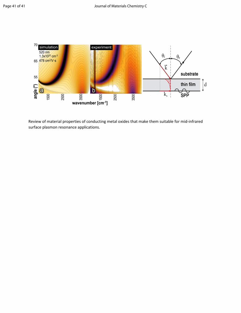
Review of material properties of conducting metal oxides that make them suitable for mid-infrared
surface plasmon resonance applications.
Page 41 of 41 Journal of Materials Chemistry C