arto hiltunen organic bulk heterojunction solar cells built on copper
TRANSCRIPT

Arto HiltunenOrganic bulk heterojunction solar cells built on copper bottomelectrodesMaster of Science Thesis
Examiner: Professor Donald LupoExaminer and subject approvedat the meeting of Faculty of Computingand Electrical Engineering Council on5 June 2013

I
TIIVISTELMÄ
TAMPEREEN TEKNILLINEN YLIOPISTOSähkötekniikan koulutusohjelmaArto Hiltunen: Kuparielektrodien käyttäminen orgaanisissa P3HT:PCBM au-rinkokennoissaDiplomityö, 48 sivuaSyyskuu 2013Pääaine: Vaihtoehtoiset sähköenergiateknologiatTarkastajat: Professori Donald Lupo ja tutkijatohtori Sampo TuukkanenAvainsanat: orgaaninen aurinkokenno, kupari, P3HT:PCBM, TiOx, ZnO, sinkkioksidi,cesium karbonaatti
Ilmastonmuutoksen hidastamiseksi EU velvoittaa jäsenmaitaan vähentämään hiili-dioksidipäästöjään 30 % vuoteen 2020 mennessä sekä 60–80 % vuoteen 2050 mennes-sä vuoden 1990 tasoon verrattuna. Sähköntuotanto aurinkosähköpaneeleilla palveli-si päästövähennystavoitteiden saavuttamista. Tänä päivänä epäorgaanisilla aurinko-kennoilla päästään helposti yli 30 % hyötysuhteisiin, mutta valmistukseen tarvitta-vien materiaalien korkea hinta ja valmistusprosessien hitaus ovat pitäneet paneelienhinnat korkealla. Kehittämällä orgaanista aurinkokennoteknologiaa, pyritään eri-tyisesti nopeampiin valmistusprosesseihin ja tätä kautta aurinkosähköjärjestelmienhuokeampaan hintaan. Nopean valmistuksen takaisi kennojen tuotanto tulostetta-van elektroniikan menetelmin.Tässä työssä tutkitaan kuparin soveltuvuutta orgaanisten aurinkokennojen elekt-rodimateriaaliksi. Tampereen teknillisen yliopiston Orgaanisen elektroniikan tutki-musryhmä on onnistuneesti valmistanut orgaanisia diodeja kuparielektrodien päälletulostettavan elektroniikan menetelmin jo vuodesta 2009 lähtien. Sillä aurinkokennoon diodi, oli tämän työn tarkoituksena tutkia kuparielektrodin soveltuvuutta aurin-kokennojen valmistukseen. Tutkimme aurinkokennojen valmistusta suoraan kupa-rielektrodin päälle ja lisäksi kokeilemme kuparin ja valoaktiivisen kerroksen välissämateriaaleja ZnO, Cs2CO3 ja TiOx. Aurinkokennojen valoaktiivisena materiaalinakäytetään P3HT:PCBM seosta.

II
ABSTRACT
TAMPERE UNIVERSITY OF TECHNOLOGYMaster’s Degree Program in Electrical EngineeringArto Hiltunen: Organic Bulk Heterojunction Solar Cells Built on Copper Bot-tom ElectrodesMaster of Science Thesis, 48 pagesSeptember 2013Major: Alternative electrical energy technologiesExaminers: Professor Donald Lupo and Academy Postdoctoral researcher Sampo Tuukka-nenKeywords: organic solar cell, copper, P3HT:PCBM, titanium suboxide, cesium carbon-ate, zinc oxide
EU obliges its member states to reduce their greenhouse gas emissions by 30 %compared to that of 1990 levels by 2020 and further 60–80 % by 2050. Electricityproduction using solar panels would help to fulfill this obligation. Today inorganicsolar cells can easily achieve energy conversion efficiencies as high as 30 % but thehigh price of inorganic solar panels has not made this technology popular. Moti-vation for developing organic solar cell technology is that it would allow the fastmanufacture of panels and this way would lead to lower solar panel market prices.The fast manufacture is achieved using the developments of printed electronics.This thesis studies the possibility to manufacture organic solar cells on copper elec-trodes. The Organic Electronics research Group of Tampere University of Tech-nology has successfully manufactured printed organic diodes on copper since 2009.Because solar cell is a diode, we wanted to study the suitability of copper as a so-lar cell electrode material. We studied the manufacture of solar cells directly oncopper but also ZnO, Cs2CO3 and TiOx was tested in between the copper and thelight active layer of the solar cell. The light active layer that we used was made ofP3HT:PCBM blend.

III
PREFACE
I could not be happier that my experiments with the “raspberry solar cell” have ledto the creation of this Master’s Thesis about organic solar cells. I am extremelyfortunate that it was Professor Donald Lupo who offered to help me with the rasp-berry project. Over the course of our collaboration, I have been graced with theopportunity to learn a great deal from him. His wisdom, expertise, support andguidance have aided me immeasurably in the process. The time I spent working inthe Organic Electronics Group under his excellent supervision has granted me themost valuable insight into organic electronics. Many thanks also go to the wholeOEG group for being such wonderful people and inspiringly talented engineers!
I would like to acknowledge the Supramolecular photochemistry research group ofTUT led by Professors Helge Lemmetyinen and Nikolai Tkachenko for allowing methe best possible conditions for conducting the experimental component of my workin their laboratory. Special thanks go to the group’s researchers who generouslyshared their wisdom in solar cell preparation with me.
My immense gratitude also goes to the whole personnel of the electromagnetics(SMG) group. Their ever helpful attitude, inspiring lectures and unwavering supporthas meant a great deal to me over the course of the past few years.
Thank you, Ossi Niemimäki, for so many things. There are far too many to listhere, but they boil down into you being the most steadfast friend a person couldhope to have. Let’s have that pint and then let’s down another, as that round’s onme! Julia Johansson, it would be a crime against good manners and taste to leaveyour name out of this preface. You mean the world to me.
During the past years I’ve met a wide array of astonishing persons who live indifferent parts of the world and whose paths only occasionally intersect with mine.I can only hope that I took the chance to tell you that I loved you when I had it.This is a one such try.
I would like to thank my dearly loved family for offering me a stable home.Having an address that is not forever changing, one at which I am always welcome,is a profoundly beautiful thing.
As a final note I would like to thank the person who wrote this quote from MarkTwain on our kitchen wall. I think it was you, Ossi.
Twenty years from now you will be more disappointed by the things youdidn’t do than by the ones you did do. So throw off the bowlines. Sailaway from the safe harbor. Catch the trade winds in your sails. Explore.Dream. Discover.
Tampere, 16 August 2013 Arto Hiltunen
IV
CONTENTS
1. Introduction . . . . . . . . . . . . . . . . . . . . . . . . . . . . . . . . . . . 12. Theoretical background of solar cells . . . . . . . . . . . . . . . . . . . . . 3
2.1 Power generation . . . . . . . . . . . . . . . . . . . . . . . . . . . . . 32.1.1 Some basic concepts of semiconductor theory . . . . . . . . . . . 52.1.2 The shape of an IV-curve . . . . . . . . . . . . . . . . . . . . . . 9
2.2 Charge generation in the active layer . . . . . . . . . . . . . . . . . . 112.2.1 The bulk heterojunction active layer . . . . . . . . . . . . . . . . 122.2.2 Ultimate efficiency . . . . . . . . . . . . . . . . . . . . . . . . . . 14
2.3 Electrodes and voltage . . . . . . . . . . . . . . . . . . . . . . . . . . 162.4 Organic electronics . . . . . . . . . . . . . . . . . . . . . . . . . . . . 172.4.1 Electrically conductive polymers . . . . . . . . . . . . . . . . . . 192.4.2 Polymer/fullerene solar cells . . . . . . . . . . . . . . . . . . . . . 19
2.5 Starting point for this work - rectifying junction in Cu organic diodes 213. Materials and methods . . . . . . . . . . . . . . . . . . . . . . . . . . . . . 23
3.1 Electrodes . . . . . . . . . . . . . . . . . . . . . . . . . . . . . . . . . 243.1.1 Copper . . . . . . . . . . . . . . . . . . . . . . . . . . . . . . . . 243.1.2 Silver . . . . . . . . . . . . . . . . . . . . . . . . . . . . . . . . . 253.1.3 ITO . . . . . . . . . . . . . . . . . . . . . . . . . . . . . . . . . . 253.1.4 Vacuum deposition . . . . . . . . . . . . . . . . . . . . . . . . . . 25
3.2 Active layer . . . . . . . . . . . . . . . . . . . . . . . . . . . . . . . . 263.2.1 Spin coating . . . . . . . . . . . . . . . . . . . . . . . . . . . . . 26
3.3 Interlayers . . . . . . . . . . . . . . . . . . . . . . . . . . . . . . . . . 273.3.1 TiOx . . . . . . . . . . . . . . . . . . . . . . . . . . . . . . . . . 273.3.2 PEDOT:PSS . . . . . . . . . . . . . . . . . . . . . . . . . . . . . 283.3.3 ZnO . . . . . . . . . . . . . . . . . . . . . . . . . . . . . . . . . . 283.3.4 Cesium carbonate . . . . . . . . . . . . . . . . . . . . . . . . . . 29
3.4 Measurement . . . . . . . . . . . . . . . . . . . . . . . . . . . . . . . 304. Results and discussion . . . . . . . . . . . . . . . . . . . . . . . . . . . . . 32
4.1 Copper-active-Ag . . . . . . . . . . . . . . . . . . . . . . . . . . . . . 324.2 Inverted solar cell with solution processed Cs2CO3 interlayer . . . . . 344.3 Inverted solar cell with solution processed ZnO interlayer . . . . . . . 384.4 Inverted solar cell with solution processed TiOx interlayer . . . . . . . 39
5. Conclusions . . . . . . . . . . . . . . . . . . . . . . . . . . . . . . . . . . . 41

V
SYMBOLS AND ABBREVIATIONS
Abbreviations
active P3HT:PCBM active layer
C60 buckminsterfullerene
DC direct current
EIL electron injection layer (hole blocking layer)
EQE external quantum efficiency
evap evaporated
FF fill factor
HIL hole injection layer (electron blocking layer)
HOMO highest occupied molecular orbit
IQE internal quantum efficiency
ITO indium tin oxide
IV-curve plot of current as a function of voltage
LiF/Al aluminum electrode enhanced with lithium fluoride
LUMO lowest unoccupied molecular orbit
MEA monoethanolamine
MEH-PPV Poly[2-methoxy-5-(2-ethylhexyloxy)-1,4-phenylenevinylene]
Milli-Q H2O ultrapure water
MIM metal-insulator-metal
MPP maximum power point
OC1C10-PPV poly[2-methoxy-5-(3’,7’-dimethyloctyloxy)-p-phenylene vinylene]
OLED organic light emitting diode
PCB printed circuit board
PCBM [6,6]-phenyl-C61-butyric acid methyl ester

VI
PC70BM [6,6]-phenyl-C71-butyric acid methyl ester
PCDTBT poly[N -9”-hepta-decanyl-2,7-carbazole-alt-5,5-(4’,7’-di-2-thienyl-2’,1’,3’-benzothiadiazole)
PCPDTBT poly[2,6-(4,4-bis(2-ethylhexyl)-4H -cyclopenta[2,1-b;3,4-b’]dithiophene)-alt-4,7-(2,1,3-benzothiadiazole)]
PEDOT:PSS poly(3,4-ethylenedioxythiophene)-poly(styrenesulfonate)
PET Polyethylene terephthalate
PLED polymer light emitting diode
PPV poly(p-phenylenevinylene)
PTAA Poly[bis(4-phenyl)(2,4,6-trimethylphenyl)amine]
P3HT poly(3-hexylthiophene)
rpm rounds per minute
sol solution process
TiOx titanium sub-oxide
TUT Tampere University of Technology
UK the United Kingdom
w% weight percent
Symbols
c speed of light
c concentration
e electron charge
eV electron volt
E electric field
Eph photon’s energy
Eg band gap
g conductivity

VII
h Planck’s constant
i electric current
imax current at MPP
I electric current
ID current through a diode
Ie current carried by the conduction band electrons
Ih current carried by holes in the valence band
IL light generated current
Isc short circuit current
I0 reverse saturation current
J current density
k Boltzmann constant
m mass
n number of electrons in the conduction band
ni intrinsic carrier concentration
p number of holes in the conduction band
P power
Pin input power
Pmax power at maximum power point
q elementary charge
Q number of quanta
Rs series resistance
T temperature
Ts temperature of a black body radiator
u voltage

VIII
umax voltage at MPP
V voltage
Voc open circuit voltage
xg variable
η energy conversion efficiency
λph photon’s wavelength
υ photon’s frequency
υg minimum frequency required for photon absorption
ϕ work function
∆V voltage loss
∆Vb sum of the voltage losses due to the band bending
Ω/ sheet resistance

1
1. INTRODUCTION
Climate Change 2007 Synthesis Report1 provided by the IPCC (IntergovernmentalPanel on Climate Change) says that warming of the climate system is certain and itis driven by increased concentrations of greenhouse gases in the atmosphere whichare due to human activity. IPCC estimates that increase of the average globaltemperature in the year 2090-2099 compared to that in 1980-1999 will be between1.1 to 6.4 degrees Celsius depending on the development scenario [1, p. 45].
The impacts of global warming will be mostly negative. Tendencies for somecereal production is previsioned to increase at mid- to high latitudes when the in-crease in temperature is less than 3 C. However "At lower latitudes, especially inseasonally dry and tropical regions, crop productivity is projected to decrease foreven small local temperature increases (1 to 2 C)". Also it is stated that "Thenegative impacts of climate change on freshwater systems outweigh its benefits". [1,p. 48–49]
European Union has decided to take measures against the climate change. Aserious negative impact on the society could be avoided, according to the EuropeanUnion, by limiting the increase in temperature below 2 C. The concrete measures tomeet the objective would be to reduce the greenhouse emissions of the EU MemberStates by 30 % compared to that of 1990 levels by 2020 and furthermore to reducethe emissions by 60 to 80 % by 2050. [2]
All this said above shall serve us as a motivation for developing photovoltaictechnology since solar cells can provide us a greenhouse gas emission free way forproducing electricity. We would like to emphasize here that we see the solar energyproduction only as a one contribute to the whole energy production along with otherenergy sources.
Classical silicon-based solar panels have proven to be efficient and stable technol-ogy even to such extent that crystalline silicon in conjunction with other inorganicphotovoltaic materials, namely gallium arsenide, have become the standard choicefor power in deep-space applications [3]. However the high manufacture costs limitthe popularity of these technologies on Earth. Organic solar cell technology is aimingto allow low cost production of solar panels.
Solar cells considered in this work fall under the class of organic photovoltaics1Next, the fifth report, is expected to be published in 2014.

1. Introduction 2
and the word organic suggest that the active material in the cell contains carbonatoms. The basis for this technology is the discovery of photoconductive polymersin the late 1970s which gave the Nobel price in Chemistry in 2000 to the researchers.
The major strength of the organic photovoltaic technology is the possibility ofpreparing parts of the cell — if not the whole cell — using printing technologies.Printing would allow fast and high yield production which would mean low man-ufacturing costs if the materials themselves were not too expensive. This is alsothe reasoning behind this work as we were seeking a way to use copper as a elec-trode material instead of ITO which is today a common choice in organic solar celltechnology.
Printing on flexible substrates would allow the solar cells, too, be flexible whichagain broadens the set of applications where the technology could be implemented.Also organic solar cells can be made semi-transparent and different colors. Thesethree last mentioned properties are a major advantage when considering applicationsin buildings or other environments where the aesthetic aspects also matters.
In chapter 2 the basic theory required to understand the working principles ofthe solar cells considered in this work is given. In chapter 3 we present the elec-trode materials, interlayer materials and the active layer materials. Also, a detailedpresentation of the preparation of the layers is given. In the end of the chapterthe measurement set up is described. In chapter 4 we give the results and discusspossible causes for the observations. Conclusions are given in chapter 5.

3
2. THEORETICAL BACKGROUND OF SOLAR
CELLS
In this chapter the theory of solar cell technology is presented to such extent thata reader should understand the working principles of solar cells in general and thenthe functioning of polymer/fullerene solar cells as a special case. Along with theorywe give some history, introduction to organic electronics and engineering aspects ofpolymer/fullerene solar cells.
2.1 Power generation
A photovoltaic cell — solar cell — is a device that can convert light into electricity.We could also say that it is a device that can under illumination provide electricpower to a load. The power P is defined by equation
P = V I,
where V is the voltage provided by the solar cell over the load and I is the electriccurrent through the load.
To be able to provide power, a solar cell must consist of something that reacts tolight such way that charge carriers are generated which can be collected at electrodesand then fed into a circuit. That one sentence description just given might seemvague but it contains just the two essential aspects that make a solar cell: i) creationof free charge under illumination and ii) collection of charge. Many devices ormaterials do one or the other but not both.
We use the term free charge in the sense that a charge is free to contribute to thecurrent flow. Doing this we avoid saying that we would actually create charges andare thus consistent with the statement that the net charge is preserved in a closedsystem [4, p. 27]. For now we shall be talking about charge or charges withoutexplicitly specifying what we mean by them. We shall define more precisely ourvocabulary in section 2.1.1.
A schematic diagram of a solar cell is presented in figure 2.1. Creation of freecharges takes place in the active layer and collection of charges is done by electrodes.
The amount of current that a solar cell can feed into a circuit depends on theamount of light incident on the cell. In an ideal case every photon incident on the

2. Theoretical background of solar cells 4
electrode 2
active layer
transparent top electrode
(a) (b)
Figure 2.1: The figure on left tries to give an idea of the minimum requirements of what onemight need to build a solar cell. On right is a sketch of a solar cell that one might preparein a laboratory. The structure is (from top to bottom) glass|transparent electrode|activelayer|electrode 2. In this particular case the active area is determined by the area of theelectrode 2 (the gray square in the middle).
active layer would contribute to the charge generation. However since a photon’senergy depends on its wavelength, not every photon possesses enough energy tocreate free charges. How much energy is needed for the creation of free charges ina material is a material property. Also the active layer materials today are limitedby their absorbance in a way that they only absorb a part of the solar spectrum.This means that even if a high energy photon was incident on the cell it might notbe absorbed. Internal quantum efficiency (IQE) and external quantum efficiency(EQE) are quantities that measure the charge production capability of a cell underillumination. They are defined as a function of wavelength the following way [5]
IQE =charge collected at electrodes
photons absorbed by the active layer
andEQE =
charge collected at electrodesphotons incident on the active layer
.
While IQE and EQE look at the behavior of the cell one wavelength at a time,as a whole the solar cell is characterized by its efficiency, η, defined as
η =Pmax
Pin,
where Pin is the solar power incident on the active area of the cell and Pmax is themaximum power output.
Every solar cell has a characteristic IV-curve (see fig.2.2) that tells us how muchpower can be attained from the cell at given point of operation (u, i) on the IV-curve.

2. Theoretical background of solar cells 5
(u, i)
Voc
|Isc|
Figure 2.2: A typical shape of an IV-curve. Geometrically the maximum power point isthe point on the IV-curve that maximizes the gray square drawn in the figure.
The point which provides the maximum power, Pmax, is called the maximum powerpoint which we denote as (umax, imax). From the IV-curve we can calculate the fillfactor FF from equation [6, p. 80]
FF =umaximax
VocIsc,
where Voc is the open circuit voltage and Isc the short circuit current. Ideally thesolar cell IV-curve would be a square determined by Voc and Isc, meaning thatthe solar cell could produce a high output current also at high voltages near Voc.Typically the current values are low near Voc as depicted in figure 2.2. Thus the fillfactor measures how close the solar cell is to an ideal device.
2.1.1 Some basic concepts of semiconductor theory
Semiconductor characteristics
Electrical properties of semiconductors lie somewhere between those of insulatorsand conductors: in normal conditions semiconductors usually conduct poorly butwhen energy is added into the system the conductivity can be increased by severalorders of magnitude. This behavior is explained by introducing the concepts ofenergy bands and band gap.
Electrons in an isolated atom are restricted to a set of discrete energy levels. Ina semiconductor crystal atoms are in close contact and as a consequence the energylevels of individual atoms interact forming energy bands where the discrete energylevels of individual atoms are so densely packed that the band appears to have acontinuous distribution of energy levels. [6, p. 17] The same way as the electron ofan isolated atom cannot have an energy value outside the set of allowed energies,electrons in a semiconductor crystal cannot be found outside the bands. The highestenergy band occupied by electrons is called the valence band and the next emptyband is called the conduction band. The difference between the highest energy level

2. Theoretical background of solar cells 6
(a) n-type (b) p-type
Figure 2.3: The effect of dopants in a semiconductor crystal. The dopant atoms are coloredgray.
of the valence band and the lowest level of the conduction band defines the bandgap.
What differentiates a semiconductor from an insulator is the size of the bandgap. The band gap of an insulator is so great that electrons cannot be excited tothe conduction by adding energy to the system. But when sufficient energy is addedto a semiconductor crystal the electrons in the valence band are able to jump thegap, enter the conduction band and contribute to the current flow. [7, p. 1598]
Electric current is flow of charges. By saying that the conduction band is emptyand the valence band is full, we mean that all the electrons are used to make bondswith the neighboring atoms and are thus bound to the crystal; they can’t movearound; they are not free to carry current. Breaking a bond frees an electron, so wesay that is has entered the conduction band. [8, p. 158–159], [6, p. 18–20]
Semiconductor properties by can be altered by adding substituents also knowas dopants into the semiconductor crystal. Dopants are atoms that contain moreor less valence electrons than the atoms that make up the semiconductor crystal.For example phosphorous and boron which contain five and three valence electronsrespectively can be used to dope silicon which has four valence electrons.
In a silicon crystal, silicon uses its four valence electrons to make covalent bondswith the neighboring Si-atoms. Also phosphorous in the Si-crystal uses four of itsvalence electrons to make the covalent bonds, leaving the fifth electron free. To beprecise, this fifth electron is hold back by the positive charge in the phosphorousnucleus, but this interaction is very weak and the electron can be freed with a verysmall amount of energy (≈ 0.02 eV) [6, p. 29]. Because the free electrons comingfrom phosphorous can easily contribute to the current flow, they are usually drawndirectly to the conduction band of the crystal in a band diagram. The act of addingnegative charge carriers into a semiconductor is called n-type doping. Atoms thatdonate the electrons are called donors.
Addition of boron in a Si-crystal leaves "a hole" into the crystal because boron

2. Theoretical background of solar cells 7
has only three valence electrons that can be used to make bonds with silicon. Anelectron that is covalently bound in the crystal can move into a hole, which movesthe hole in that place where the electron originally was [9]. Thus the movementof an electron can be seen as the movement of a hole and vice versa, from whichfollows that we can consider the movement of holes as a contribute to the currentflow.1 In the energy band diagram, holes are drawn into the valence band or in thedirect vicinity [6, p. 29]. Engineering holes into a semiconductor is called p-typedoping, and the p-type dopants are called acceptors since they accept the electronsfrom the adjacent atoms. [8, p. 159–160] The effect of dopants is illustrated in figure2.3. Because this phenomenon is of personal interest, the discussion is ended witha direct quote from Pearson and Bardeen: [9, p. 866]
The missing electron, or hole, behaves in all respects like a particlewith a positive charge equal in magnitude to the electron charge. It hasinertia, momentum, and energy corresponding to a mass of the sameorder as the mass of an electron. – – The only essential difference is inthe sign of the mobile charge.
Majority and minority charge carriers
The way doping effects the energy band diagrams is presented in figure 2.4. N-type doping increases the number of conduction band electrons and p-type dopingintroduces holes into the valence band. Figure 2.4(a) shows the situation in anintrinsic (i.e. undoped) semiconductor relative to the doped ones. For an idealizedintrinsic semiconductor holds [6, p. 26]
n = p = ni,
where p is the number of holes in the valence band, n is the number of electronsin the conduction band and ni is called the intrinsic carrier concentration that hasbeen measured to be 1.00 · 1010 cm−3 for silicon [11].
The definitions for majority and minority charge carriers are established fromfigure 2.4. In the n-type semiconductor the major part of the current is carried bythe conduction band electrons, while the holes in the valence band have a smallercontribution to the current. Thus, we define that in a n-type semiconductor electronsin the conduction band are majority carriers and holes in the valence band areminority carries. Using the same logic, we define that in a p-type semiconductor theholes in the valence band are majority carriers and electrons are minority carriers.
1Note however that the only charge carriers are electrons but sometimes, if we decide to do so,we may regard the flow of electrons as the flow of fictious particles called holes [10, p. 226]. Wewill often choose to do so. For a more profound treatment the reader is referred to [10].

2. Theoretical background of solar cells 8
valence bands(a) undoped
valence bands
conduction bands
(b) p-type
valence bands(c) n-type
Figure 2.4: The effect of doping semiconductors. P-type semiconductor has an increasednumber of holes in the valence band and the n-type semiconductor has an increased numberof free electrons in the conduction band. In reality the number of holes and electrons inan undoped semiconductor is around 1 · 1010 cm−3.
[12, p. 84–85]The total current density J in a semiconductor is given as
J = Je + Jh,
where Je is the current carried by conduction band electrons and Jh is the currentcarried by holes in the valence band [6, p. 34]. Notice that charges of opposite signsmust flow in opposite directions in order to contribute to a current flow in the samedirection. This is a corollary of the definition of electric current [4, p. 163].
The pn-junction
The pn-junction is the basis for several electronic devices, also for solar cells. As thename suggest, a pn-junction is formed by joining a p-type and a n-type semicon-ductor together. When the junction is formed, the free electrons near the junctionin the n-type side diffuse into the holes near the junction in the p-type side. Then-type dopant atoms near the junction that lost electrons in the diffusion processbecome positively charged. Similarly, the p-type dopants that accepted the dif-fused electrons become negatively charged. This charging forms a potential acrossthe junction that eventually prevents a further flow of charge. We can model thepotential with an electric field that is directed from n-side to p-side. [12, p. 170]
By definition the direction of an electric field is such that it points at the directionwhere the flow of positive charge is assisted. It follows that in a pn-junction theformed electric field opposes the flow of holes from the p-side to the n-side and the

2. Theoretical background of solar cells 9
E
barrier for electrons in the n-side
e− e− e− e−
e−no barrier for electrons in the p-side
p-side n-side
barrier for holes
Eg
Figure 2.5: The energy bands of a pn-junction. The dashed line in the middle shows thejunction and Eg is the band gap of the semiconductor. Superimposed is the direction ofthe electric field E inside the junction.
flow of electrons from the n-side to the p-side. Hence, the electric field opposes theflow of majority charge carriers across the junction. But both sides contain a smalldensity of minority charge carriers, electrons in the p-side and holes in the n-side,that are aided across the junction by the electric field.
Another way to explain the functioning of a pn-junction is to consider the energybands across the junction. In figure 2.4 we drew the energy bands with a straightgray block. When a pn-junction is formed, the energy bands bend. The situation isillustrated in figure 2.5. We see that due to the band bending the majority chargecarriers on both sides feel a barrier that they should cross in order to get to theother side of the junction. The minority charge carriers feel no barrier on eitherside. [7, p. 1610], [12, p. 170–171]
The flow of charge carriers across the junction can be controlled by applying abias voltage across the junction. Forward biasing a pn-junction means applying apositive voltage on the p-type side of the junction and negative on the n-type side.Forward biasing assists the flow of majority charge carriers over the junction whilereverse biasing decreases the flow of majority charge carriers. [8, p. 160–163]
2.1.2 The shape of an IV-curve
In this section we shall try to find an explanation for the shape of an IV-curve of asolar cell. It is possible to measure two different IV-curves: one under illuminationand one in dark.
The dark curve of a solar cell resembles the IV-curve of a diode and obeys thuswell the diode equation [12, p. 184]

2. Theoretical background of solar cells 10
−0.2 −0.1 0 0.1 0.2 0.3 0.4 0.5
−0.015
−0.01
−0.005
0.005
0.01
0.015
0.02
V
A darkilluminated
(a)
E
p nIDIL
RI
.(b)
Figure 2.6: a) Plots of equations 2.1 (dashed) and 2.3 (solid line) as a function of V .I0 = 10−9 A, IL = 10 mA, T = 300 K, V ∈ [−0.2, 0.6]. b) Currents in an illuminatedpn-junction and the net current I.
ID = I0(eqV/kT − 1) (2.1)
where, ID is the current through the diode, V is the voltage over the diode, I0the reverse saturation current, q the elementary charge, k the Boltzmann constant(≈ 1.381 · 10−23 J/K) and T the temperature. Indeed, solar cells are diodes apartfrom the differences in the optical properties. The graph of ID is plotted in figure2.6(a) with dashed lines. It’s important to notice that ID consists mostly of majoritycharge carriers.
Photons that have energy greater than the band gap of the semiconductor ma-terial will increase the number of minority and majority charge carriers on both, pand n, sides but only the minority charge carriers are aided across the junction bythe E-field. As a result a light generated current, IL, that consists of the increasednumber of minority charge carriers that drift across the junction, grows greater thanID and the IV-curve falls into the fourth quadrant in figure 2.6(a). While the biasvoltage is increased in the forward direction, more and more majority charge carriersare flowing across the junction and ID is suddenly increased over IL. Directions ofI and ID are shown in figure 2.6(b).
When the solar cell is operated in the fourth quadrant the product of current andvoltage becomes negative, which means that power is extracted from the solar cell.Based on the discussion above we can present the first model for the IV-curve of asolar cell as

2. Theoretical background of solar cells 11
I = ID − IL (2.2)
= I0(eqV/kT − 1)− IL. (2.3)
ID and I are plotted in figure 2.6(a). Equation 2.3 was proposed as early as 1955 byBell Telephone Laboratories that had build the very first silicon based pn-junctionsolar energy converter one year earlier [13].
To be precise, in the original publication [14] equation 2.3 was to describe anequivalent circuit model for a solar cell that would consist of a diode (ID) connectedin paraller with a constant current source (IL). Most of the time this circuit isstill the basis of equivalent circuit models that try to describe the behavior of anymodern solar cell: dye-sensitized [15] or organic [16].
2.2 Charge generation in the active layer
This thesis is dealing with devices whose active layer is made of donor and acceptormaterials, namely from polymer and fullerene respectively. Next we describe thefunctioning of this type of active layer in more detail. (See section 2.4.2 to find outhow we and others have come to this choice of active layers). We draw some analogybetween organic and inorganic semiconductor theory.
Solar cells are energy converters2 and they are able to do this conversion due theirability to absorb photons of certain energy and transfer that energy to electrons ina semiconductor. A photon’s energy, Eph, is given as [7, p. 1453]
Eph =hcλph
= hυ,
where h is the Planck’s constant, c the speed of light, λph the photon’s wavelengthand υ the photon’s frequency.
Probability for a photon absorption is high if the photon’s energy is higher thanthe band gap of the semiconductor. Absorption of photons with smaller energiesis low because inside the band gap there is no allowed states where the electroncould be excited. When a photon is absorbed by the semiconductor it increases theelectron’s energy by the amount of its own energy, Eph, so that the electron canleave the valence band and enter the conduction band. The electron that has quitthe valence band leaves behind a hole. Thus absorption of a photon leads to creationof an electron-hole pair. [12, p. 119] The photon absorption process is illustrated infigure 2.7(a).
2In fact the first modern articles in 1950s that were written about the topic talked about "solarenergy converters" rather than solar cells. See for example [14].

2. Theoretical background of solar cells 12
photon
valence band
conduction band
Eg
HOMO acceptor
(a) Inorganic semiconductor
HOMO donor
LUMO donorLUMO acceptor
HOMO acceptor
(b) Organic donor-acceptor heterojunc-tion
Figure 2.7: Band diagrams and photon absorption in inorganic and organic semiconduc-tors.
Using the language of organic chemistry it is common practice to talk aboutHOMO (highest occupied molecular orbit) and LUMO (lowest unoccupied molec-ular orbit) levels instead of valence and conduction bands. However the schematicpresentation of electron transfer between the levels or bands is very similar as can beseen comparing figures 2.7(a) and 2.7(b). It can be seen that when the active layeris constructed from two materials, donor and acceptor, the electron is transferredfrom donor to acceptor.
2.2.1 The bulk heterojunction active layer
Absorption of a photon in an inorganic semiconductor leads directly in creation ofan electron-hole pair [17]. However in organic semiconductors the formation of anelectron-hole pair is proposed to happen via successive steps which we must considerif we are aiming to build efficient solar cells. Despite the debate3 within the scientificcommunity concerning the steps of this process we next present one sequence thatdescribes the charge generation in polymer/fullerene solar cells that is provided inreference [19]. We will look into more detail at a special kind of active layer calledthe bulk heterojunction.
According to [19], absorption of a photon by the polymer (donor) creates anexciton which can move about in the donor phase a distance called the excitondiffusion length. If the exciton encounters a donor-acceptor interface before decayingit is transformed into a electron-hole pair, that might still be Coulombically bound,where the electron is in the acceptor phase and the hole in the donor phase. Theelectron-hole pairs are then separated into free charges with the aid of electrodes;
3Pointed out for example by Dennler and Sariciftci in [18].

2. Theoretical background of solar cells 13
electrode
electrode
electrode
electrode
Figure 2.8: Author’s illustration of the bulk heterojunction. Stars present the excitonscreated in the donor(polymer) material by photons. Donor material is colored green andacceptor material red. On right, one of the excitons has reached a donor-acceptor interfaceand separated into a electron-hole pair. Electron is drawn with the black circle and holewith white circle.
anode collecting the hole and cathode collecting the electron.A source for controversy has been whether the excitons dissociate into Coulombi-
cally bound electron-hole pairs or directly into free charge carriers. In reference [20]it is concluded that in P3HT/PCBM devices the exciton dissociation leads directlyinto a formation of free charge carriers but in reference [21] the authors, three ofwhom also contributed to the previous article, conclude that in PCPDTBT/PC70BMdevices the electron-hole pairs are Coulombically bound. Thus, it seems that thequestion is actually case dependent.
The bulk heterojunction is described to consist of a network of internal donor-acceptor heterojunctions. Because separation of excitons into electron-hole pairshappens at the donor-acceptor interface, the idea behind bulk heterojunctions isthat there would always be an interface within the exciton diffusion length [22]which is estimated to be around 14 nm [23]. The charge separation process in bulkheterojunction solar cells is illustrated in figure 2.8.
Although the structure might seem complex, the functioning of the bulk het-erojunction active layer can be analyzed using the energy level concept depictedin figure 2.7. Moreover, for modeling purposes the bulk heterojunction has beenthought to be just one semiconductor; the HOMO level of donor being equivalentto the valence band and LUMO level of acceptor being the conduction band. Thisapproach has been used for example in reference [24].

2. Theoretical background of solar cells 14
2.2.2 Ultimate efficiency
We shall next consider the ultimate efficiency of a solar cell. More precisely, we shallpresent an approximation for the amount of energy that could be harvested fromsolar irradiation using one pn-junction — using one band gap. The analysis willbe based solely on the celebrated article by Shockley and Queisser from 1961 [25].Although their analysis concerns inorganic devices, that were under intense studyat the time, we see no reason why this analysis wouldn’t apply to organic deviceswithin the frame of the assumptions that have been made. The assumptions are
1. The solar cell has a circular shape and it is surrounded by a blackbody oftemperature Ts. See figure 2.9.
2. The solar cell is held at temperature 0 K.
3. Only photons that have energy greater than the semiconductor band gap areabsorbed. The amount of energy that is absorbed equals the band gap of thesemiconductor.
solar cellblack body, Ts = 6000 K
Figure 2.9: Solar cell and radiation source geometries.
Photons with different energies arrive in different amounts. The idea of theultimate efficiency calculation is to find that band gap value which can absorb thosephotons that carry the largest portion of the available energy. A small band gapsemiconductor will absorb a large part of the irradiation spectrum but the amountof energy that is harvested for energy production stays low because the amount ofthe photon’s energy that exceeds the band gap is lost in the semiconductor latticein scattering events. [12, p. 119] The idea is elucidated in figure 2.10.
The calculation begins with considering the number of quanta Q (m−2s−1) thathave a energy greater than the band gap Eg = hυg. This equals the number ofabsorbed photons. Q is calculated by integrating the Planck distribution from υg toinfinity:
Q =2π
c2
∫ ∞υg
υ2
ehυ/kT − 1dυ. (2.4)
It is possible to simplify the integrand by introducing a new symbol, xg, defined asxg = hυg
kT . Substituting xg along with dx = hkT dυ into 2.4 gives

2. Theoretical background of solar cells 15
Eg3
Photon energy
Eg2
Band gap
Energy lost
Energy captured
Eg1
Figure 2.10: The height of the arrow describes the energy of the incident photon. For theband gap values apply Eg3 > Eg2 > Eg1.
Q =2π(kT )3
h3c2
∫ ∞xg
x2
ex − 1dx.
The total energy carried by the quanta, originating from the black body, can becalculated from 2.4 by multiplying the formula with hυ and integrating it over thewhole frequency range from zero to infinity:
Pin =2πhc2
∫ ∞0
υ3
ehυ/kT − 1dυ,
which yields the Stefan-Boltzmann law [7, p. 1475]
=2π5(kT )4
15h3c2.
Now we are ready to calculate the efficiency η as a function of xg from equation
η(xg) =Pout
Pin=hυgQ(xg)
Pin,
where Pout is the output power of the solar cell that is estimated to equal the amountof photons absorbed times the energy that can be harvested per photon.
In [25] a neat analytical solution is found for 2.4. We chose to perform thecalculations numerically using MATLAB. The results are given in figure 2.11. Theultimate efficiency 44 % is found at xg= 2.2 which corresponds to a band gap valueof about 1.1 eV, which could be calculated from relation
xg =hυg
kTs=
qVg
kTs.
The band gap of silicon is approximately 1.1 eV [41, p. 12–80] which makes siliconan optimal material for solar energy conversion in the light of this analysis. In

2. Theoretical background of solar cells 16
organic bulk heterojunction solar cells the difference between the donor HOMO leveland acceptor LUMO level is approximately 1.9 eV which gives 33 % for ultimateefficiency. Based on the assumptions of this section, a significant improvement in theorganic solar cell conversion efficiency could be expected if the LUMO and HOMOlevels of the active layer materials could be engineered to give a smaller "band gap".However our analysis is very much simplified. The optimum band gap value will bedifferent from 1.1 eV when more variables are taken into account. A more detailedanalysis is also included in [25].
0 0.5 1 1.5 2 2.5 3 3.50
5
10
15
20
25
30
35
40
45
Vg (eV)
Effi
cien
cy (
%)
0 1 2 3 4 5 6 7
0
5
10
15
20
25
30
35
40
45
xg
Figure 2.11: Ultimate efficiency
2.3 Electrodes and voltage
So far we have concentrated on the free charge creation in the active layer and havenot said much about the collection of charge, except that it happens at electrodes.We look at that part now.
In the solar cells under study the current is carried by both electrons and holes.In order to make the charges of opposite signs contribute to the net current flow inthe same direction, the charges — electrons and holes — must be lead to oppositedirections in the device. This is a corollary of the definition of electric current [4,p. 163]. The situation is established by choosing electrodes with different workfunctions [19]. Holes diffuse towards the electrode with higher work function andelectrons towards the electrode with lower work function (see figure 2.12).
The way electrode work functions are situated relative to the HOMO and LUMOlevels of the semiconductor results in two different contact types between the mate-rials : ohmic and non-ohmic.
When the work function, ϕ, of an electrode is below the LUMO level of acceptoror above the HOMO level of donor (such as depicted in fig. 2.12(a)) are the metal-semiconductor contacts said to be non-ohmic. In this case the maximum attainablevoltage, Voc, is obtained from the work function difference of the electrode materials

2. Theoretical background of solar cells 17
HOMOdonor
LUMOacceptor
ϕ1
ϕ2
(a) non-ohmic contacts
ϕ1
ϕ2
(b) ohmic contacts
Figure 2.12: Two different metal-semiconductor contacts are shown. In addition the flowof free charge carriers in the device is pictured.
which is in accordance with the metal-insulator-metal (MIM) model for solar cells.[26] Written into an equation we get
Voc =ϕ2 − ϕ1
q, (2.5)
where ϕ2 and ϕ1 are the electrode work functions and q is the elementary charge.If the electrode work functions are close to the donor HOMO and acceptor LUMO
levels as in fig. 2.12(b) an ohmic contact is formed. Each ohmic contact contributesa voltage loss, ∆V , which reduces the maximum obtainable voltage from the solarcell. The voltage loss is explained to be caused by accumulated charges at thecontact which results in energy level band bending in the semiconductor. [26] Wewrite this into an equation4 the following way
Voc =HOMOdonor − LUMOacceptor
q−∆Vb, (2.6)
where ∆Vb is the sum of the voltage losses due to band bending and the HOMOand LUMO levels are supposed to be given as absolute values. In ref [27] Scharberet al. test 26 different bulk heterojunction solar cells and end up experimentally inan equation for Voc which is similar to equation 2.6.
2.4 Organic electronics
Organic electronics is a field that extends over a broad set of applications whichinclude organic photovoltaics, flexible displays, lighting products, electronics & com-ponents and Integrated Smart Systems as illustrated in figure 2.13. To define whatis meant by organic electronics we quote the OE-A Roadmap [28, p.4]
Organic electronics is based on the combination of a new class of mate-4In ref [26] the authors give this equation to a particular device, namely
|glass|ITO|PEDOT:PSS|OC1C10-PPV:PCBM|LiF/Al|.

2. Theoretical background of solar cells 18
Figure 2.13: Visioned development of organic electronics according to [28, p.1].
rials and large area, high volume deposition and patterning techniques.Often terms like printed, plastic, polymer, flexible, printable inorganic,large area or thin film electronics - - are used, which essentially all meanthe same thing: electronics beyond the classical approach.
In organic photovoltaics, the manufacturing of solar cells using printing processesis one of the most desired features since it would allow fast high yield productionwhich would result in lower manufacturing costs. Printing is allowed if a materialcan be deposited from solution. These solutions are called inks.
Even though organic electronics has several nice features, a few key challenges arelimiting this technology’s entry in consumer electronics. First thing to be improved isthe electrical performance of organic materials. As an example the highest reportedconductivity, g, of PEDOT:PSS is 1.418 · 105 S/m [29] which is more than hundredtimes smaller than the conductivity of copper gCu ≈ 6 · 107 S/m (calculated usingresistivity of 1.67 ·10−8 Ωm for copper [4, p.168]). An other big issue that should beovercome in the future is the stability of materials. [28, p.3] Proposed degradationmechanisms include photodegradtion of the active layer and a reaction between theactive layer and the electrode material. In addition, preparation and storage of thesolar cells in ambient air is known to decrease their performance. [30] The stabilityissues create a need for proper encapsulation methods — which preferably shouldbe as low-cost as possible.

2. Theoretical background of solar cells 19
2.4.1 Electrically conductive polymers
We are used to think of plastics — polymers — as insulating materials, but this viewis getting old as conductive polymers are making their way into consumer electron-ics. The starting point for this technology can be traced back to 1977 when in anarticle [31] titled Electrical Conductivity in Doped Polyacetylene, a "dramatic" in-crease in the conductivity of polyacetylene via doping was reported. Among authorswere Professors Heeger, MacDiarmid and Shirakawa who were awarded with the No-bel Prize in Chemistry in 2000 for their pioneering work in this field. After 1977Heeger and MacDiarmid continued their work with polyacetylene from which theycould build a photoelectrochemical solar cell in 1979 [32]. However it was not until1990 when a group of scientists from University of Cambridge built a light-emittingdiode from poly(p-phenylenevinylene) (PPV) that has multiplied and reignited theresearch activity in the field of conductive polymers. This revolutionary article [33]was authored by Burroughes, Bradley, Brown, Marks, Mackay, Friend, Burns andHolmes and published in Nature titled Light-emitting diodes based on conjugatedpolymers. Above described breakthroughs have allowed the growth of organic elec-tronics into its own field of engineering and form also the basis for our interest —solar cells.
2.4.2 Polymer/fullerene solar cells
Usually it is considered that the benchmark for organic solar cell conversion effi-ciency was set by Tang in 1985 when he reported in reference [34] a small moleculebased heterojunction5 solar cell with about 1% conversion efficiency. It took longtime before polymer solar cells could reach the limit set by Tang. In 1993 Sariciftciet al. reported a heterojunction polymer solar cell using MEH-PPV as donor andC60 as acceptor that could reach 0.04 % efficiency. The breakthrough happenedin 1995 when Yu et al. presented in reference [22] the first bulk heterojunctionsolar cells that were by two orders of magnitude more efficient than their prede-cessors, reaching 2.9 percent efficiency 6. Since then the bulk heterojunction hasbecome standard technology in the field of polymer solar cells. Let us now lookmore closely at the basic engineering solutions that enable high efficiencies. At thetime of writing this thesis Polyera holds the world record in efficiency, 9.1 %, withtheir polymer/fullerene organic photovoltaic cell. Heliatek has reached 12.0 % with
5Often Tang is also incorrectly known as the first one to ever build a heterojunction solarcell. However Tang himself points out in his arcticle that "The first two-layer photovoltaic systemappears to be that reported by D.R. Kearns and M. Calvin in J.Chem. Phys. 29, 950 (1958)"
6Yu et al. calculate the efficiency using formula ηe = FF ·VocIscPin
, where they define FF as∫ Voc
0IdV. This results in the following definition for efficiency ηe = 1
Pin
∫ Voc
0IdV which is different
from our definition η = PmaxPin
.

2. Theoretical background of solar cells 20
their small molecule cell.
Active layer materials
The work horse acceptor material has been the fullerene derivative [6,6]-phenyl-C61-butyric acid methyl ester (PCBM) and a common donor material has beenpoly(3-hexylthiophene) (P3HT). [18] These materials were chosen to be the activelayer materials in this work as well. Originally, fullerene derivatives were preferredover pure C60 because of their better solubility and better film forming propertieswhen deposited from solution [22].
Materials that have become more popular just recently include [6,6]-phenyl-C71-butyric-acid methyl ester (PC70BM) and poly[N -9”-hepta-decanyl-2,7-carbazole-alt-5,5-(4’,7’-di-2-thienyl-2’,1’,3’-benzothiadiazole) (PCDTBT) that were successfullyused to produce a solar cell with 6.1 % power conversion efficiency and internalquantum efficiency close to 100 %. The increased efficiency is due to the smallerband gap between donor and acceptor that enables the active layer to absorb a largerfraction of solar spectrum. An other advantage that these materials have over theconventional ones is that they don’t require thermal annealing to achieve optimummorphology. [35] (See experimental section 3.2 for more detailed description ofpreparation of active layers).
Interlayers
Interlayers are used in organic solar cells to better direct the holes and electrons inopposite directions which results in increased current. They fall into two categories:electron injection layers (EIL) and hole injection layers (HIL). An electron selectivecontact can be achieved by choosing semiconductors whose valence band energiesare too low compared to the HOMO level of donor to allow hole injection. A holeselective contact is created by choosing a semiconductor whose conduction band istoo high compared to the LUMO level of the acceptor. Obviously, no barrier shouldexist in order to allow the injection of desired charges. Successfully used EILs havebeen prepared for example from TiOx [36] and ZnO [37]. Succesfully used HILshave been made from MoO3 and V2O5 [38]. See section 3 for detailed descriptionof materials used in this work. Figure 2.14 shows the conduction and valence bandsof interface layers relative to the donor-acceptor active layer’s HOMO and LUMOlevels.
The discussion above was about interlayers made of semiconducting materials.Other materials that are known to improve the performance of organic solar cellsare, among others, the conductive polymer PEDOT:PSS and caesium carbonate.PEDOT:PSS has been used as an HIL in a same manner than above mentioned

2. Theoretical background of solar cells 21
HOMOdonor
LUMOacceptor
ϕ1
ϕ2
EIL
HIL
barrier for electrons
barrier for holes
Figure 2.14: Illustration of the energy level alignment of HILs and EILs.
semiconductive materials. Caesium carbonate, however, has the interesting propertyto be able to alter the work function of the electrode on top of which it is deposited.We will return to these topics in chapter 3.
2.5 Starting point for this work - rectifying junction in Cuorganic diodes
The spark for this project was the successful manufacture of printed organic diodesthat used copper cathodes. In these devices the semiconductor, PTAA, and thetop electrode made of silver ink were gravure printed on a copper cathode whichhad been sputtered on a PET substrate, giving the diode structure: |Cu|PTAA|Ag|.[39] Since the work functions of silver and copper are both close to the HOMOlevel of PTAA no rectification should happen under proper bias conditions. It wasfound that the rectifying behavior was due an initially unintentional dual-dielectriclayer between the copper and PTAA. First layer was Cu2O that was caused bythe oxidation of copper and the second dielectric layer resulted from the defects onthe PET substrate and perhaps from the PET itself. In the end it was concludedthat the method would allow the production of printed organic diodes. [40] Sinceprinting is seen as a way to produce low-cost devices, the scope of this thesis was tostudy the suitability of copper cathodes for solar cell applications. We also visionedthat making the copper bottom electrode work would allow the replacement ofexpensive ITO cathodes with more affordable copper and thus further reduce themanufacturing costs of solar cells.

2. Theoretical background of solar cells 22
Figure 2.15: IV-curves of Cu|PTAA|Ag-diodes with different semiconductor thicknesses.The copper was sputtered on a PET substrate. Adopted from [39].

23
3. MATERIALS AND METHODS
In this chapter we introduce all the main materials that were used to build the solarcells studied in this thesis. We also describe the deposition methods. All the studiedsolar cell structures are presented in figure 3.1.
The solar cells were built on glass substrates, 5 cells on one substrate. The sizeof the glass substrates was 1 mm × 12 mm × 35 mm. The substrates used in cellse and f had an ITO coating. Prior to usage all the substrates were cleaned withsonication in acetone, cloroform, sodium lauryl sulfate solution (20 mg sodium laurylsulfate in 500 ml Milli-Q H2O), Milli-Q H2O and 2-propanol for 30 minutes in eachsolution. Substrates were then dried in vacuum at 150 C for 1 hour.
AgP3HT:PCBM
Cuglass
(a)
AgP3HT:PCBMCs2CO3 (sol)
Cuglass
(b)
AgP3HT:PCBM
ZnOCuglass
(c)
AgP3HT:PCBM
TiOx
Cuglass
(d)
AgP3HT:PCBM
ZnOITOglass
(e)
CuCs2CO3 (evap)P3HT:PCBMPEDOT:PSS
ITOglass
(f)
Figure 3.1: Block presentations of every solar cell studied in this thesis. Light enters thecells through the silver electrode in the cells where a copper bottom electrode is used (a–e).In (e–f) light enters the cells through the ITO bottom electrode. Abbreviations sol andevap refer to the deposition methods: solution processing and evaporation.

3. Materials and methods 24
35 mm
1 mm
12 mm(a) (b)
Figure 3.2: On left is presented the dimensions of a substrate and the shape of a bottomelectrode. On right is depicted the way 5 individual solar cells were built on one substrate.Blue color presents the glass substrate, orange the bottom electrode, red the active layerand gray the top electrodes. The active area of the first solar cell is highlighted with blackcolor.
3.1 Electrodes
The shape of the bottom electrode is shown in figure 3.2(a) with gray color. In cellsa-d (fig.3.1) the copper electrode was evaporated on the cleaned substrates using amask (Scotch Magic Tape 810) to cover the part that we wanted to keep clean fromcopper. In cells e and g the electrode was etched into shape in aqua regia
Milli-Q H2O : HNO3 : HCl = 5 : 0.4 : 4.6
in volume ratios. Temperature of the aqua regia bath was 50 C and bathing timewas 7 min. The part of the ITO that we wished to keep was protected with threelayers of nail polish.
3.1.1 Copper
Copper in its pure form, Cu, has a work function value in the range of 4.53 eV –4.94 eV depending on the surface orientation [41, 12–108]. The work function ofthe copper cathodes in the diodes discussed in section 2.5 was measured to be 4.8eV when they were prepared by evaporation [42]. We believe this value is the bestestimate for the work function of copper cathodes in our solar cells too.
Copper tends to oxidize easily and it was found out that the Cu electrode of thediodes were covered with a Cu2O layer [40]. Cu2O (cuprite or copper(I) oxide) isa semiconducting mineral with a very high resistivity value ranging from 10 Ωm to50 Ωm [41, 12–87]. But, due to cuprite’s semiconducting property a photoresponsehas been obtained in p-Cu2O/n-ZnO heterostructure films [43]. In that work, theauthors got a high control over the crystallographic structure of the Cu2O layerusing rf-magnetron sputtering with a controllable oxygen flow rate and proper post-treatments. They conclude that the well oriented crystallographic structure is the

3. Materials and methods 25
key factor leading to their success. In the case of the diodes, the cuprite layer growsin an uncontrolled manner on top of the Cu electrode due to the oxygen in ouratmosphere.
Copper electrodes were vacuum deposited on cleaned glass substrates. The layerswere made 35 nm thick.
3.1.2 Silver
Silver, Ag, has a work function of 4.52 eV to 4.74 eV depending on the surfaceorientation [41, 12–108]. The measured value for the silver ink used in the diodes(section 2.5) differs from the value given in the textbooks which is explained to becaused by the oxidation of silver. The measured value for the work function of thesilver anode was 5.2 eV. [42] We use this work function value for the silver anodesof our solar cells in this work. The solar cells were illuminated through the silverelectrode when the bottom electrode was made of copper. This is possible if thesilver layer is not made too thick.
Silver electrodes were vacuum deposited on top of the active layer. The layerswere made 25 nm thick.
3.1.3 ITO
ITO, indium tin oxide, films are transparent and electrically conductive which makesthem suitable for uses in LED and photovoltaic devices. Actually, ITO has been thechoice for electrode material since the dawn of OLED and PLED technology (seefor example [44] and [33]), and even before it was used in LCDs.
The work function of around1 4.4 eV – 4.5 eV [45] enables the use of ITO as eitheranode or cathode together with a suitable counter electrode. The sheet resistanceof the ITO coated glass substrates that we used was 10 Ω/.
3.1.4 Vacuum deposition
Vacuum deposition is a method to produce thin films with very good control of thethickness of the layers. In the vacuum deposition unit used in this work (EdwardsAuto306) the samples, i.e. the solar cells under preparation, are attached to therotating sample holder that is held from the ceiling of the vacuum chamber.
A suitable amount of a material to be evaporated (Cu, Ag or Cs2CO3 ) is placed ina "cup" made of molybdenum through which an electric current can run. The cupsare known as evaporation sources or boats. The current heats up the evaporationboat and the substance, which finally results in the formation of, for example, copper
1There is variation in the reported values for ITO work function. For example 4.7 eV is reportedin reference [38].

3. Materials and methods 26
vapor inside the vacuum chamber. The rate at which the material is deposited canbe monitored, and was typically few nanometers per minute. Vacuum before thestart of the evaporation was typically ≈ 10−6 mbar.
3.2 Active layer
The active layer was chosen to be donor-acceptor bulk heterojunction type. Thedonor material used was poly(3-hexylthiophene) i.e. P3HT purchased from Merckunder the product name SP001 LISICON and the acceptor material used was [6,6]-phenyl-C61-butyric acid methyl ester i.e. PCBM purchased from Merck under theproduct name of PV-A600 LISICON.
Preparation
The mass ratio in the final precursor solution that we used for the active layer was
m(PCBM)m(P3HT)
=0.8
1,
in which the concentrations, c, of P3HT and PCBM were c(PCBM) = 14.222 mg/mland c(P3HT) = 17.778 mg/ml.
The final precursor solution was prepared by first measuring PCBM and P3HTin their respective test tubes and dissolving them in 1,2-dichlorobenzene. Argon gaswas then injected into the both tubes before closing them. Next the both solutionswere stirred for over night at 50 C with a rate of 500 rmp. Solutions were combinedthe next morning to give the final precursor described above which was then stirredfor 4 h at 70 C with 300 rpm followed by stirring over night at 50 C with a rateof 500 rpm. 1 hour before spin coating the temperature of the solution was againincreased to 70 C and the stirring rate to 750 rpm.
Spin coater settings were 500 rpm, 5 min and medium acceleration (012). Afterspin coating the layers were annealed in vacuum (≈ 10−3 mbar) at 110 C for 10minutes.
3.2.1 Spin coating
Spin coating is an easy way to produce thin films on small-scale substrates from aprecursor solution. The precursor is injected on the substrate which is then spun(10 – 10 000 rmp) to spread the precursor solution on the substrate evenly.
The substrate is held at place with the aid of a vacuum chuck, in other wordswith suction, on top of which fragment adapters can be employed to have bettergrip on substrates of different sizes.
3. Materials and methods 27
The spin coater used in this work was WS-400-6NPP from Laurell TechnologiesCorporation. Nitrogen flow was set up into the spin coater chamber to protect thesamples from impurities and air during the process.
3.3 Interlayers
3.3.1 TiOx
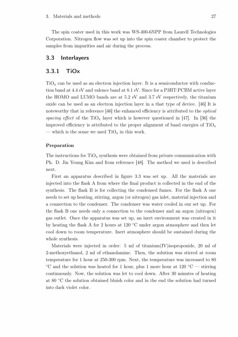
TiOx can be used as an electron injection layer. It is a semiconductor with conduc-tion band at 4.4 eV and valence band at 8.1 eV. Since for a P3HT:PCBM active layerthe HOMO and LUMO bands are at 5.2 eV and 3.7 eV respectively, the titaniumoxide can be used as an electron injection layer in a that type of device. [46] It isnoteworthy that in reference [46] the enhanced efficiency is attributed to the opticalspacing effect of the TiOx layer which is however questioned in [47]. In [36] theimproved efficiency is attributed to the proper alignment of band energies of TiOx
— which is the sense we used TiOx in this work.
Preparation
The instructions for TiOx synthesis were obtained from private communication withPh. D. Jin Young Kim and from reference [48]. The method we used is describednext.
First an apparatus described in figure 3.3 was set up. All the materials areinjected into the flask A from where the final product is collected in the end of thesynthesis. The flask B is for collecting the condensed fumes. For the flask A oneneeds to set up heating, stirring, argon (or nitrogen) gas inlet, material injection anda connection to the condenser. The condenser was water cooled in our set up. Forthe flask B one needs only a connection to the condenser and an argon (nitrogen)gas outlet. Once the apparatus was set up, an inert environment was created in itby heating the flask A for 2 hours at 120 C under argon atmosphere and then letcool down to room temperature. Inert atmosphere should be sustained during thewhole synthesis.
Materials were injected in order: 5 ml of titanium(IV)isopropoxide, 20 ml of2-methoxyethanol, 2 ml of ethanolamine. Then, the solution was stirred at roomtemperature for 1 hour at 250-300 rpm. Next, the temperature was increased to 80C and the solution was heated for 1 hour, plus 1 more hour at 120 C — stirringcontinuously. Now, the solution was let to cool down. After 30 minutes of heatingat 80 C the solution obtained bluish color and in the end the solution had turnedinto dark violet color.

3. Materials and methods 28
flask A
flask B
Figure 3.3: The apparatus that was used for TiOx precursor solution preparation. Adoptedfrom [48].
Next morning2 the two step heating from 80 C to 120 C was repeated and alow-density gel was obtained, as wished for. After the solution had cooled down toroom temperature, 10 ml of methanol was injected into the flask A to extract theTiOx precursor, "the final transparent" (see [48]). The solution separated into twoliquid phases of which we collected the upper one.
Solution was spin cast using program: 2000 rpm, 1 min, slow acceleration. Thefilm was then let to hydrolyze in air over night.
3.3.2 PEDOT:PSS
PEDOT:PSS, poly(3,4-ethylenedioxythiophene):poly(styrenesulfonate), is a conduc-tive polymer that can be used as a hole injection layer in P3HT:PCBM devices dueits high work function. The conductivity of PEDOT:PSS has been increased upto 1418 S cm−1 using ethylene glycol treatment. This high conductivity value al-lows the use of PEDOT:PSS as a stand alone electrode. [29] The work function ofPEDOT:PSS is around 5.2 ± 0.1 eV [49, 19-27].
3.3.3 ZnO
ZnO can be used an as electron injection layer in a similar manner to TiOx. Theconduction band and valence band energies for ZnO are 4.2 eV and 7.5 eV, respec-tively [37]. Using the method proposed in [37] the optical transmittance of solutionderived ZnO layers can be increased up to 95 %. Solution derived ZnO layers werefirst introduced to organic photovoltaic device applications in reference [50].
2In the instructions the synthesis was completed without pauses

3. Materials and methods 29
Preparation
Our ZnO precursor solution contained 50 mg/ml of zinc acetate (C4H6O4Zn · 2H2O)dissolved in a solution which was 96 % 2-methoxy ethanol and 4 % ethanolamine.Final product was stirred at 70 C, 500 rpm for 2 hours and was then let settle downover night. Prior to spin coating the precursor solution was filtered using a 0.2 µmfilter. Spin coater settings were 2000 rpm, 1 min and slow acceleration (001).
After spin coating the samples were annealed at 300 C in air for 5 min and thenrinsed with Milli-Q H2O, ethahol and acetone. As a final step the samples weredried at 300 C for 3 minutes.
ZnO precursors without the ethanolamine component and without the high tem-perature annealing were also prepared.
3.3.4 Cesium carbonate
Cesium carbonate (caesium carbonate, UK), Cs2CO3, can be used to lower the workfunction of the electrode on which it is deposited. This allows the production ofefficient cathodes even from materials that have a considerably high work function.It is also known to enhance the electron injection of usual cathode materials suchas aluminum. Interlayers made of Cs2CO3 can be prepared by thermal evaporationor by deposition from solution but the properties of the formed layers vary slightly.
It has been shown that thermally deposited Cs2CO3 decomposes to CsO2 and ce-sium suboxides. The formed layer is a n-type semiconductor with high conductivity.The properties of the caesium carbonate films prepared by thermal evaporation aremainly attributed to its decomposition products meaning that the work function ofvarious material’s can be modified because a chemical reaction between the electrodematerial and ceasium carbonate is not needed to lower the work function.
The situation is different when caesium carbonate is deposited using solution pro-cesses without thermal annealing treatments because then Cs2CO3 doesn’t decom-pose into CsO2. However when caesium carbonate layer is deposited on a reactivemetal, such as aluminum, it has been observed to form Al–O–Cs complexes whichare able to lower the work function and increase the electron injection properties ofthe electrode to same extent as thermally evaporated layers of caesium carbonate.Due the desired decomposition products, especially Cs2O, a thermal annealing treat-ment has been proposed for solution processed caesium carbonate layers in reference[51]. [52]
Preparation
Cs2CO3 layers were deposited either from solution using spin coating or by evapora-tion. The layer thickness prepared by evaporation was 3 nm. Solution process was

3. Materials and methods 30
IL
ID
v1Rs
V
AI
solar cell
DC power supply
Figure 3.4: SMU measurement of a solar cell under illumination. When the cell is notilluminated IL = 0 and the voltage drop across Rs is reversed. The arrowhead pointstowards the positive end of the resistor. Equivalent circuit of the solar cell is drawn insidethe dashed box.
adopted from reference [51]. The precursor solution was prepared simply dissolving0.2 weight percent (w%) of Cs2CO3 in 2-ethoxyethanol which was then spin coatedwith settings 2000 rpm, 1 min, slow acceleration. The sample was then heated on ahotplate for 20 minutes at 155 C.
3.4 Measurement
IV-curves were measured using a Agilent E5272A SMU (Source Measure Unit).SMUs are able to output the sweep voltage or current and measure the dc voltageor current simultaneously.
A simplified set up for a SMU measurement is shown in figure 3.4. The idea isto set a voltage sweep, V ∈ [umin, umax], against the output voltage of the measuredsample and then record the value of the output current i at each u to get a set of(u,i)-pairs that graph the IV-curve. The short circuit current is obtained when theapplied voltage is zero. And the open circuit voltage is read from the point wherethe current is zero. More formally,
Isc = i | u = 0Voc = u | i = 0.
Another method get the IV-curve is to connect the output of the solar cell over avariable resistance, R ∈ [0, Rmax] where Rmax is so great that practically no currentcan pass through it and then record all the (u,i)-pairs at each value of R.
Looking at the measured IV-curves given in chapter Results, one sees that theydo not quite obey the equation I = I0(eqV/kT −1)−IL, and one reason for this is themeasurement set up that we are using. When electric current flows through the solar

3. Materials and methods 31
cell it faces resistance the same way it would do flowing through any material havingresistivity different from zero. We call this resistance the series resistance, Rs, andwe have added it into the equivalent circuit model for the solar cell in figure 3.4.This resistance affects the measurement in different ways during the measurementin dark and under illumination.
The situation under illumination is shown in figure 3.4. When the solar cellis operated in the fourth quadrant, IL is greatest current in the circuit so the netcurrent flows against the direction of I and is thus measured negative. This directionof net current flow causes a voltage drop over the diode and as a result we record avoltage that is smaller than the junction voltage by the amount of the voltage drop,v1. [53]
Situation is different when the solar cell is measured in dark. Now IL = 0 sothe current flows from the DC power supply into the direction of I. Now, since thevoltmeter is before the voltage drop v1, the recorded values for voltage are higherthan what actually was applied over the junction. [53] This is one reason why theIV-curves measured under illumination are not simply shifted below the dark curveby the amount of IL, as is predicted by the equation I = I0(eqV/kT − 1)− IL.

32
4. RESULTS AND DISCUSSION
4.1 Copper-active-Ag
A solar cell with structure Cu|P3HT:PCBM|Ag was built to serve as a reference forthe experiments with interlayers that will be described in the following sections. 2out of 10 solar cells worked right after the preparation, but only one after 48 hours.The IV-curve of this solar cell and its performance data is presented in figure 4.1(a)and table 4.1. Figure 4.1(b) shows three representative IV-curves from the samebatch that were not able to produce output power.
The open circuit voltage, Voc, of this solar cell is very low, which was expectedfrom theory. Using equation 2.5 we can calculate the predicted open circuit voltageto be
Voc =ϕ2 − ϕ1
q=
5.2 eV− 4.8 eVe
= 0.4 V,
which is close to what we got, taking into account the incertitudes in the values usedfor work functions. If the low voltage was easily explained, the low current densityleaves more room for speculation.
The work functions of copper and silver are quite close to each other compared tofor example, Al and ITO, Al and PEDOT:PSS, and LiF/Al and ITO which are morecommon choices for electrode materials and are known to produce high performancedevices (see for example [35], [29] and [27]). The small work function differencebetween copper and silver might not be enough to efficiently transport the electronsand holes to the right electrodes; electrode collected at the anode doesn’t contributepositively to the net current. Also, if the electrons and holes are inefficiently leadinto opposite directions, that means increased risk of recombination. Finally, thesemiconducting, high resistance, Cu2O layer that grows on top of the copper elec-trode due oxidation might grow so thick that a major part of current is lost there.Moreover, the oxidation rate is accelerated as a function of temperature. Eventhough this structure doesn’t have interlayers that require annealing treatments,the active layer is heated at 110 C for 10 minutes in low vacuum (≈ 10−3 mbar)during which the copper bottom electrode is also exposed to this temperature. Thelow oxygen content in the oven of course decelerates the oxidation process. Goodtreatment on the oxidation of copper is given in [54].

4. Results and discussion 33
Table 4.1: Performance
Structure Efficiency % FF Voc (V) Jsc(mA/cm2)Cu|P3HT:PCBM|Ag 0.30 50 0.30 -0.74
−0.2 −0.1 0 0.1 0.2 0.3 0.4 0.5 0.6−1
−0.5
0
0.5
1
1.5
2
2.5
3
3.5
4
Voltage (V)
Cur
rent
den
sity
(m
A/c
m2 )
darkilluminated
(a)
−0.2 −0.1 0 0.1 0.2 0.3 0.4 0.5 0.6−400
−200
0
200
400
600
800
1000
1200
Voltage (V)
Cur
rent
den
sity
(m
A/c
m2 )
darkilluminateddarkilluminateddarkilluminated
(b)
Figure 4.1: IV-curves of structure Cu|P3HT:PCBM|Ag after 48 hours from preparation.On left, the only one that worked from 10 prepared samples. On right, three representativeIV-curves of those that didn’t work. Notice that the active layer is still able to inject chargesin the solar cell that is marked with red.
From the data plotted in figure 4.1(b) we can calculate the resistance that thecurrent feels going through the actual device of size 0.02 cm2. The resistance isapproximately 30 ohms, which is high enough to exclude the possibility that a directcontact between the electrodes was formed because of careless preparation. But wesee that the current is more than 200 times higher compared to the working solar cellwhich means that low resistance paths from electrode to electrode are formed insidethe device at some point during the preparation or before measurement. Lookingcarefully at the lines marked with red, we see that the current is higher underillumination than in dark which we take as an evidence that the active layer stillworks and is able to inject charges.
We now propose that the problem is the degradation of the copper electrode —which is initiated by oxidation — and that the active layer is not damaged in any ofthe structures tested. Next we present an explanation for the lines in figure 4.1(b)and in the following sections we shall be taking a stand on how the interlayer understudy did or did not prevent this degrading process from happening.
In reference [55] it was reported that oxygen from the atmosphere penetrates thesilver electrode and diffuses trough the device to the back electrode "within a fewminutes". This means that the active layer and the silver top electrode are not

4. Results and discussion 34
Cu active Ag
metal oxide
organic-metalcomplex
Figure 4.2: We propose that the resistance trough the cell diminishes as a consequenceof diffusion of the electrode materials into the active layer. This would explain the highcurrents in figure 4.1(b).
able to protect the copper from oxidation. Further, it has been shown in [56] thatsolar cells that use aluminum electrodes thicken by 3.2 nm within 9 hours which iscaused by two subsequent processes: 1) formation of aluminum oxide and 2) reactionbetween aluminum oxide and the organic active layer. The condition for the secondreaction to happen is the first one and because we know that a layer of copperoxide is formed in our solar cells, it is then possible that the copper oxide wouldreact with the organic layer. Also, the reaction between silver, which oxidizes too,and the organic layer has not been ruled out. This said, it is now possible that inour Cu|P3HT:PCBM|Ag structure we might have the thickening process going onat both electrodes. As a consequence the reaction products would diffuse into theactive layer and this way lower the resistance trough the solar cell. This processis illustrated in figure 4.2. What supports this explanation is the fact that layersin solar cells are known to intermix. Traces of aluminum and indium was foundthroughout a device that was built between aluminum and ITO electrodes. [57].
4.2 Inverted solar cell with solution processed Cs2CO3 inter-layer
Table 4.2: Performance
Structure Efficiency % FF Voc (V) Jsc(mA/cm2)Cu|Cs2CO3(sol)|P3HT:PCBM|Ag 0.18 44 0.24 -0.63
In this section we consider a structure Cu|Cs2CO3(sol)|P3HT:PCBM|Ag, wherethe notation Cs2CO3(sol) means that the cesium carbonate layer was depositedfrom solution. The solar cell was built on a glass substrate with evaporated copper

4. Results and discussion 35
−0.2 −0.1 0 0.1 0.2 0.3 0.4 0.5 0.6−1
0
1
2
3
4
5
Voltage (V)
Cur
rent
den
sity
(m
A/c
m2 )
darkilluminated
(a) 1 h
−0.2 −0.1 0 0.1 0.2 0.3 0.4 0.5 0.6−200
−100
0
100
200
300
400
500
Voltage (V)
Cur
rent
den
sity
(m
A/c
m2 )
darkilluminated
−0.2 −0.1 0 0.1 0.2 0.3 0.4 0.5−0.1
0
0.1
0.2
0.3
0.4
0.5
0.6
0.7
0.8
0.9
Voltage (V)
Cur
rent
den
sity
(m
A/c
m2 )
dark
(b) 15 h
Figure 4.3: IV-curves of a solar cell with structure Cu|Cs2CO3 (sol)|P3HT:PCBM|Ag (a)1 hour and (b) 15 hours after preparation.
bottom electrode. Directly after evaporation of copper, Cs2CO3 interlayer and theP3HT:PCBM active layer were deposited from solution, using methods that weredescribed earlier, followed by evaporation of silver top electrode.
Table 4.2 shows the performance of the best cell in the prepared batch and figure4.3 shows the IV-curves 1 hour and 15 hours after preparation. We see that theperformance of the structure is similar to that without the interlayer, but this time80 % of the cells worked right after preparation. However, degradation of the deviceswas fast: half of the cells in the batch lost their photovoltaic properties completelyin 15 hours as in figure 4.3(b) and the other half showed degraded performance inthe measurement.
Figure 4.3(b) reveals us that the problem is in the electrodes, more precisely inthe Cu-Cs2CO3 electrode since the silver electrode has been proved to work. Silverelectrodes are used widely as a part of TUT Department of Chemistry’s solar cellresearch. When measured in the dark, the shape of the IV-curve looks as if it wasrectifying which is shown in the inset but actually the leakage current has increased100 times of what it was right after the preparation, from 1.24 · 10−8 A to 1.23 ·10−6 A. However the active layer still clearly works — it is able to inject charges —since the current under illumination has increased from that of dark.
Because we know from measurement that the dark current is not linear, it is clearthat the solar cell is not completely short circuited. On the other hand, we see thatthe current in the cell is higher after 15 hours from preparation than right afterwhich again means that a low resistance path or paths are formed in the cell for thecurrent.
One reason for the poor performance of the device might be that copper is notreactive enough to form Cu–O–Cs complexes; in reference [52] the high efficiency of

4. Results and discussion 36
devices were attributed to formation of element–O–Cs complexes when a solutionprocess was used. In the same work the authors conclude that silver is not reac-tive enough to form Ag–O–Cs, and were not able to produce efficient PLEDs fromCs2CO3 modified silver cathodes. In the periodic table copper is in the same columnas silver (and gold) which means that these materials should have similar chemicalproperties [58, p.33], and thus all be not reactive enough for the purpose.
Later in ref [51] it was shown that a thermal annealing treatment would benefit thefunctioning of solution processed cesium carbonate layers because the Cs2CO3 woulddecompose into CsO2 which was thought to be the reason for increased performancewhen thermal evaporation was used. That is why an annealing treatment (20 min,155 C in air) was done for all samples. One might think that this extra annealingtreatment plus the annealing of the active layer would completely oxidize the copperelectrode and prevent the solar cell from working at all, but interestingly 80 % ofthe prepared solar cells worked as already mentioned which is a considerably highernumber of working solar cells than without the cesium carbonate layer.
We explain this improvement in the number of working solar cells with the aidof electrochemistry. (Notice, that in the calculation we are assuming the existenceof elemental cesium, Cs, in the film. One might argue if this is actually the case.)Consider the reduction potentials of the following half-reactions [41, p. 8–17]
Cu2O + H2O + 2 e− → 2 Cu + 2 OH− E = −0.360 VCs+ + e− → Cs E = −3.026 V
According to theory, a net reaction that produces a positive voltage difference ∆E
is spontaneous [58, p. 465]. So we get,
Cu2O + H2O + 2 e− → 2 Cu + 2 OH− E = −0.360 V2 Cs → 2 Cs+ + 2 e− E = 3.026 V
Cu2O + H2O + 2 Cs → 2 Cu + 2 OH− + 2 Cs+ ∆E = 2.666 V
The positive value after the last reaction means that a reaction where oxidizedcopper, Cu2O, is reduced to clean copper, Cu, with the aid of cesium is spontaneous.We believe that this reduction reaction protects the copper electrode during theannealing treatments and some hours after the completion of the solar cell. Thesolar cells will start degrading because cesium and its compounds are known to beunstable1 in ambient air [59, p. 308], [60].
For curiosity, solar cells having top electrode from copper were built. The com-plete structure was ITO|P3HT:PCBM|Cs2CO3(evap)|Cu, where (evap) means that
1According to [59]: "Cesium. – – Oxidizes rapidly in air; in moist air may ignite spontaneously"

4. Results and discussion 37
Table 4.3: Performance of solar cells where cesium carbonate was evaporated
Structure Efficiency % FF Voc (V) Jsc(mA/cm2)ITO|PEDOT:PSS|P3HT:PCBM|Cs2CO3 |Cu 1.0 44 0.27 -3.23
ITO|P3HT:PCBM|Cs2CO3 |Cu 0.7 43 0.34 -1.83
−0.2 −0.1 0 0.1 0.2 0.3 0.4 0.5 0.6−5
0
5
10
15
20
25
Voltage (V)
Cur
rent
den
sity
(m
A/c
m2 )
darkilluminatedafter 30 daysafter 30 days
Figure 4.4: IV-curves of ITO|P3HT:PCBM|Cs2CO3 (evap)|Cu solar cell right after prepa-ration (dark) and one month after preparation (red).
the cesium carbonate was evaporated. This way the copper electrode wasn’t ex-posed to heating at any point during the process. PEDOT:PSS was used in onebatch to enhance the efficiency of the structure. The results are given in table 4.3and figure 4.4. The obtained efficiencies were higher than in any other structurethat we tried because of the transparent ITO electrode through which the cell wasilluminated. The interesting observation here is that all the prepared samples wereable to keep their rectifying property in dark even one month after the preparation.This observation supports the proposition that annealing treatments accelerate thedegrading processes whenever copper electrodes are used.
Another interesting thing is to consider the work functions of ITO and copperthat are 4.4 – 4.5 eV and 4.8 eV respectively. Based on these values solely one mightexpect the ITO to be the cathode. However, the evaporated Cs2CO3 is able to lift thework function of copper above ITO’s and make the Cu electrode the cathode. Thisconfirms the potential of cesium carbonate as an electrode modifier and broadens thechoice of counter electrode materials that could be used with copper. Because theopen circuit voltage correlated with the work function difference of the electrodes,this finding now opens the speculations for getting higher voltages from coppercells: using Cs2CO3 to lower the work function of copper and choosing a high workfunction material such as PEDOT:PSS as an anode, might lead to higher voltagesand improved efficiency.

4. Results and discussion 38
Table 4.4: Performance of ITO|ZnO|P3HT:PCBM|Ag
Structure Efficiency % FF Voc (V) Jsc(mA/cm2)ITO|ZnO|P3HT:PCBM|Ag 2.44 57 0.54 -2.94
−0.2 −0.1 0 0.1 0.2 0.3 0.4 0.5 0.6−4
−3
−2
−1
0
1
2
3
Voltage (V)
Cur
rent
den
sity
(m
A/c
m2 )
darkilluminated
(a) ITO|ZnO|P3HT:PCBM|Ag
−0.2 −0.1 0 0.1 0.2 0.3 0.4 0.5 0.6−100
−50
0
50
100
150
200
250
300
Voltage (V)
Cur
rent
den
sity
(m
A/c
m2 )
darkilluminated
(b) Cu|ZnO|P3HT:PCBM|Ag
Figure 4.5: a) ZnO precursor without MEA, annealed at 170 C was shown to workequally efficiently as the standard method. b) This method however didn’t work on solarcells having copper electrodes.
4.3 Inverted solar cell with solution processed ZnO interlayer
Attempts to build solar cells with structure Cu|ZnO|P3HT:PCBM|Ag were unsuc-cessful. The usual method to produce ZnO layers (see section 3.3.3) has been shownto increase the efficiency of organic solar cells in several works. We believe thatthe method was not suitable for our structure because of the 300 C annealingtemperature and the ethanolamine component used in the precursor solution.
Copper oxidizes in air and the oxidation rate is accelerated as a function oftemperature. In our experiments, when the copper electrodes were taken out of theoven their color had turned from copper to green, meaning that they were badlyoxidized. The oxidation products, Cu2O and CuO, are semiconductors with highresistivity. So, when a severe oxidation happens copper loses its property to act asan electrode with a desired work function since it now acts as an insulator.
Ethanolamine (MEA, monoethanolamine) is a strong base [59, p. 3676] andit is said to act as a stabilizer in a ZnO precursor solution [61]. It also allowsdissolution of higher zinc acetate concentrations in 2-methoxy ethanol, which wasused as a solvent. We observed that precursor solutions which contained the 4 %of ethanolamine damaged the copper electrode immediately when the solution wasapplied on the electrode surface. It was known that MEA has the ability to dissolvecopper and that it has been used in printed circuit board (PCB) etching [62] but

4. Results and discussion 39
beforehand it was not obvious whether the 4 % in total volume would be crucialamount for our electrodes.
To overcome the problems caused by high temperature annealing and MEA, pre-cursor solutions without MEA were prepared and lower annealing temperatures weretried. It was possible to dissolve 30 mg/ml of zinc acetate in 2-methoxy ethanolwithout MEA. Using this precursor and 170 C annealing temperature, solar cellswith structure ITO|ZnO|P3HT:PCBM|Ag produced a good photoresponse. A rep-resentative IV-curve is given in figure 4.5(a) and the performance data is listedin table 4.4. Even lower annealing temperatures started to decrease the efficiencyconsiderably. The new precursor with 170 C annealing temperature was tried onCu|ZnO|P3HT:PCBM|Ag structure, but no rectifying behavior was obtained. Wesee from the IV-curve (fig. 4.5(b)) that the solar cell reacts to light but is not ableto produce any power due to the lack of rectifying property.
In the light of what has been said in the two preceding sections we concludesimply that the ZnO layer is not able to decelerate the degradation processes thatwill damage the copper electrode. In theory zinc should be able to reduce copper,but it seems that for our purposes the reaction is not strong or fast enough. In theperiodic table and in the electrochemical series zinc is closer to copper than cesiumor titanium which produced working solar cells, which supports the hypothesis ofslow reaction.
4.4 Inverted solar cell with solution processed TiOx interlayer
In this section we consider a structure Cu|TiOx|P3HT:PCBM|Ag, where the TiOx
was spin cast from a precursor solution. As a reference, TiOx was also tested onITO. The results are summarized in table 4.5 and in figure 4.6. It is seen that,the performance is similar to what we got with structures Cu|P3HT:PCBM|Ag andCu|Cs2CO3 |P3HT:PCBM|Ag ; low voltage is due small work function differencebetween the electrodes, which also partly explains the small current in additionto the fact that the solar cell is illuminated through 25 nm thick silver electrode.Noteworthy is that the efficiency of the ITO device (3) is relatively low, which mightindicate that something went slightly wrong during the synthesis of the precursormeaning that higher efficiencies could be possible achieve.
Again most important findings were obtained in terms of stability. Contrary toany other interlayer we found that TiOx on top of copper improved the efficiencyafter one week storage period. Small variations in the Jsc value might be causedby variations in the lamp power during the measurement but because the opencircuit voltage has increased as well we have a reason to believe that the increasein efficiency can be merited to the TiOx layer. None of the measured solar cellproduced "straight line" IV-curve that we saw with other structures in the previous

4. Results and discussion 40
sections.The ability of TiOx to improve device lifetimes is attributed to its ability to
actively remove O2 and H2O from a device. Moreover after approximately a oneday of storage in air the TiOx layer transforms from hydrophilic to hydrophobic,and is now able to prevent further intrusion of water or oxygen into the device. Theuse of TiOx layer in PLEDs or organic solar cells increases the lifetime of a deviceapproximately two orders of magnitude. [48]
It is thus possible that TiOx could reduce Cu2O to Cu owing to its oxygen scav-enging property and that it would prevent further flow of oxygen or moisture intothe device during storage, which would explain the results we have obtained.
Table 4.5: Performance. The IV-curves of solar cells number 3 and 1 are given in figures4.6(a) and 4.6(b).
Structure Efficiency % FF Voc (V) Jsc(mA/cm2)1 Cu|TiOx|active|Ag 0.20 45 0.25 -0.67after a week 0.24 44 0.26 -0.78
2 Cu|TiOx|active|Ag 0.18 43 0.24 -0.64after a week 0.19 41 0.27 -0.65
3 ITO|TiOx|active|Ag 1.32 42 0.38 -3.05after a week 1.14 41 0.35 -2.93
−0.2 −0.1 0 0.1 0.2 0.3 0.4 0.5 0.6−4
−3
−2
−1
0
1
2
3
4
Voltage (V)
Cur
rent
den
sity
(m
A/c
m2 )
darkilluminateddark, after one weekilluminated, after one week
(a) 3 ITO|TiOx |P3HT:PCBM|Ag
−0.2 −0.1 0 0.1 0.2 0.3 0.4 0.5 0.6−1
0
1
2
3
4
5
6
7
8
Voltage (V)
Cur
rent
den
sity
(m
A/c
m2 )
darkilluminateddark, after one weekilluminated, after one week
(b) 1 Cu|TiOx |P3HT:PCBM|Ag
Figure 4.6: Left, ITO/TiOx reference solar cell suffered from minor degradation duringstorage time. Right, unlike any other structure that was tested the Cu/TiOx electrodedidn’t degrade while stored and was able to produce power even after a one week.

41
5. CONCLUSIONS
The goal of the present work was to study the suitability of copper as an electrodematerial in solar cell applications. Four different cases were investigated: a copperelectrode without any modification, copper modified by TiOx, Cs2CO3 or ZnO.
It was found out that the thin copper oxide layer that grows in between theelectrode and the active layer during the manufacturing process prevents the solarcells from working if the electrode is left unmodified. Deposition of TiOx or Cs2CO3
film on top the copper electrode allows the preparation of working solar cells whileZnO does not.
We proposed that the oxide layer initiates a reaction between the active layerand the electrodes which leads to the diffusion of the electrode materials into theactive layer. This process might allow the formation of filament like paths fromelectrode to electrode that would explain the short circuit like behavior of some ofthe samples.
In the Cu|PTAA|Ag-diodes that were the inspiration for this work a copper oxidelayer is also formed but since the diodes are operated at higher bias voltages, thecharges are able to tunnel through the oxide layer. We believe that the few hundredmillivolts that we got out of the prepared solar cells is not enough to allow tunneling.
Cesium carbonate and TiOx allow the production of working solar cells by re-ducing the oxide layer thickness. But due to the instability of cesium carbonatein air, the solar cells degraded fast. Looking forward, it would be interesting tostudy whether stability could be achieved by preparing the solar cells under inertatmosphere and using a proper encapsulation. VTT (Technical Research Centre ofFinland) has a pilot roll to roll inert atmosphere printing machine [63], so giventhat stability was achievable via manufacture in inert conditions, the production ofprinted organic solar cells on copper would be possible.
In the light of this work TiOx appears to be the most attractive choice as anelectrode modifier since it can reduce the oxide layer thickness, it is stable in air andit forms a protective layer which doesn’t pass oxygen nor moisture through. In addi-tion, TiOx doesn’t require thermal annealing treatments unlike cesium carbonate orZnO. We believe that the ZnO layer didn’t work because the annealing temperatureit requires, is too high for copper.
As a final note we conclude the following: it is possible to prepare organic solar

5. Conclusions 42
cells on copper electrodes using a proper electrode modifier for which Cs2CO3 andTiOx were found suitable. For stability, inert manufacture conditions should bestudied.

43
BIBLIOGRAPHY
[1] Climate Change 2007: Synthesis Report. An Assessment of the In-tergovernmental Panel on Climate Change. http://www.ipcc.ch/pdf/assessment-report/ar4/syr/ar4_syr.pdf (visited on 12.8.2013)
[2] Decision No 406/2009/EC of The Europian Parliament and of the Council.23 April 2009. On the effort of Member States to reduce their greenhouse gasemissions to meet the Community’s greenhouse gas emission reduction com-mitments up to 2020. http://eur-lex.europa.eu/LexUriServ/LexUriServ.do?uri=OJ:L:2009:140:0136:0148:EN:PDF (visited on 12.8.2013)
[3] Dave Doody. Basics of Space Flight. National Aeronautics and Space Admin-istration. Available http://www2.jpl.nasa.gov/basics/editorial.php (vis-ited on 12.8.2013)
[4] J.R. Reitz, F.J. Milford and R.W. Christy. Foundations of ElectromagneticTheory. 4th ed. Addison–Wesley, 1993.
[5] G. Dennler, K. Forberich, M. Scharber, C. Brabec, I. Tomis, K. Hingerl, T.Fromherz. Angle dependence of external and internal quantum efficiencies inbulk-heterojunction organic solar cells. J. Appl. Phys. 102 054516 (2007)
[6] M.A. Green. Solar cells: operating principles, technology, and system applica-tions. Kensington: University of New South Wales, 1998.
[7] H.D. Young, R.A. Freedman. Sears and Zemansky’s University Physics withModern Physics. 11th ed. Pearson;Addison-Wesley, 2004.
[8] N. Storey. Electronics a systems approach. 2nd ed. Pearson;Prentice Hall, 1998.
[9] G. L. Pearson and J. Bardeen. Electrical Properties of Pure Silicon and SiliconAlloys Containing Boron and Phosphorus. Physical review, vol. 75 number 5March 1. 1949.
[10] N.W. Ashcroft, N.D. Mermin. Solid state Physics. Saunders College, 1987.
[11] A.B. Sproul and M.A. Green. Improved value for the silicon intrinsic carrierconcentration from 275 to 375 K. J. Appl. Phys. 70, 846 (1991).
[12] B.G. Streetman, S.K. Banerjee. Solid state electronic devices. 6th ed. Pear-son;Prentice Hall, 2006.

BIBLIOGRAPHY 44
[13] D.M. Chapin, C.S. Fuller, and G L. Pearson. A New Silicon pn Junction Pho-tocell for Converting Solar Radiation into Electrical Power. J. Appl. Phys. 25,676 (1954).
[14] M.B. Prince. Silicon Solar Energy Convertes. J. Appl. Phys. 26 534-540 (1955).
[15] Tian Hanmina, Zhang Xiaoboa, Yuan Shikuia, Wang Xiangyana, TianZhipenga, Liu Bina, Wang Yinga, Yu Taoa, Zou Zhiganga. An improvedmethod to estimate the equivalent circuit parameters in DSSCs. Solar Energy83 715–720 (2009).
[16] A. Cheknane, H. S. Hilal, F. Djeffal, B. Benyoucef, J-P Charles. An equivalentcircuit approach to organic solar cell modeling. Microelectronics Journal 391173-1180 (2008).
[17] B. A. Gregg and M. C. Hanna. Comparing organic to inorganic photovoltaiccells: Theory, experiment, and simulation. J. Appl. Phys. 93, 3605 (2003).
[18] G. Dennler and N. Sariciftci. Flexible Conjugated Polymer-Based Plastic SolarCells: From Basics to Applications. Proceedings of the IEEE (Volume:93 , Issue:8 ) 1429 - 1439 (2005).
[19] Blom, Mihailetchi, Koster and Markov (2007), Device Physics of Poly-mer:Fullerene Bulk Heterojunction Solar Cells. Adv. Mater., 19: 1551-1566.
[20] J. Kniepert, M. Schubert, J. C. Blakesley, D. Neher. Photogeneration and Re-combination in P3HT/PCBM Solar Cells Probed by Time-Delayed CollectionField Experiments. Journal of Physical Chemistry Letters J. Phys. Chem. Lett.,2 (7), pp 700–705 (2011).
[21] Steve Albrecht, Wolfram Schindler, Jona Kurpiers, Juliane Kniepert, James C.Blakesley, Ines Dumsch , Sybille Allard , Konstantinos Fostiropoulos , UllrichScherf , and Dieter Neher. On the Field Dependence of Free Charge CarrierGeneration and Recombination in Blends of PCPDTBT/PC70BM: Influence ofSolvent Additives. J. Phys. Chem. Lett. , 2012, 3 (5), pp 640–645
[22] G. Yu, J. Gao, J. C. Hummelen, F.Wudl, A.J. Heeger. Polymer PhotovoltaicCells: Enhanced Efficiencies via a Network of Internal Donor-Acceptor Hetero-junctions. Science, New Series, Vol.270, No. 5243 (Dec. 15, 1995), 1789-1791.
[23] A. Haugeneder, M. Neges, C. Kallinger, W. Spirkl, U. Lemmer, and J. Feld-mann, U. Scherf, E. Harth, A. Gügel, and K. Müllen. Exciton diffusion and dis-sociation in conjugated polymer/fullerene blends and heterostructures. Phys.Rev. B 59, 15346–15351 (1999).

BIBLIOGRAPHY 45
[24] L. J. A. Koster, E. C. P. Smits, V. D. Mihailetchi, and P. W. M. Blom . Devicemodel for the operation of polymer/fullerene bulk heterojunction solar cells.Phys. Rev. B 72, 085205 (2005).
[25] W. Shockley and H. J. Queisser. Efficiency of a p-n Junction Solar Cells. J.Appl. Phys. 32, 510-519 1961.
[26] V. D. Mihailetchi, P. W. M. Blom, J. C. Hummelen, and M. T. Rispens. Cath-ode dependence of the open-circuit voltage of polymer:fullerene bulk hetero-junction solar cells. J. Appl. Phys. 94, 6849 (2003).
[27] Scharber, Mühlbacher, Koppe, Denk, Waldauf, Heeger and Brabec,(2006), De-sign Rules for Donors in Bulk-Heterojunction Solar Cells — Towards 10%Energy-conversion Efficiency. Adv. Mater., 18: 789-794.
[28] White Paper "Roadmap for Organic and Printed Electronics". 4th ed. 2011.Available at http://www.oe-a.org/en_GB/downloads. (visited on 16.8.2013)
[29] Kim, Y. H., Sachse, C., Machala, M. L., May, C., Müller-Meskamp, L. and Leo,K. (2011), Highly Conductive PEDOT:PSS Electrode with Optimized Solventand Thermal Post-Treatment for ITO-Free Organic Solar Cells. Adv. Funct.Mater., 21: 1076–1081
[30] Pathways for the degratation of organic photovoltaic P3HT:PCBM based de-vices. Matthew O. Reese, Anthony J. Morfa, Matthew S. White, Nikos Kopi-dakis, Sean E. Shaheen, Garry Rumbles, David S. Ginley. Solar Energy Mate-rials 6 Solar Cells 92 (2008) 746–752.
[31] C. Chiang, C. Fincher, Y. Park, A. Heeger, H. Shirakawa, E. Louis, S. Gau, A.MacDiarmid. Electrical conductivity in doped polyacetylene. Physical reviewletters. vol. 39. number 17. 1977.
[32] S.N. Chen, A.J. Heeger, Z. Kiss, A. G. MacDiarmic, S. C. Gau and D.L. Peebles.Polyacetylene, (CH)x:Photoelectrochemical solar cell. Appl. Phys. Lett. 36, 96(1980)
[33] Light-emitting diodes based on conjugated polymers. J.H. Burroughes, D. D.C. Bradley, A. R. Brown, R. N. Marks, K. Mackay, R. H. Friend, P. L. Burns& A. B. Holmes. Nature 347, 539 - 541 11 October (1990).
[34] C.W. Tang. Two-layer organic photovoltaic cell. Appl. Phys. Lett. 48, 183(1986).
BIBLIOGRAPHY 46
[35] Sung Heum Park, Anshuman Roy, Serge Beaupré, Shinuk Cho, Nelson Coates,Ji Sun Moon, Daniel Moses, Mario Leclerc, Kwanghee Lee & Alan J. Heeger.Bulk heterojunction solar cells with internal quantum efficiency approaching100 % Nature Photonics 3, 297 - 302 (2009).
[36] C. Waldauf, M. Morana, P. Denk, P. Schilinsky, K. Coakley, S. A. Choulis,and C. J. Brabec. Highly efficient inverted organic photovoltaics using solutionbased titanium oxide as electron selective contact. Appl. Phys. Lett. 89, 233517(2006).
[37] A. K. K. Kyaw, X. W. Sun, C. Y. Jiang, G. Q. Lo, D. W. Zhao, and D. L.Kwong. An inverted organic solar cell employing a sol-gel derived ZnO electronselective layer and thermal evaporated MoO3 hole selective layer. Appl. Phys.Lett. 93, 221107 (2008).
[38] Vishal Shrotriya, Gang Li, Yan Yao, Chih-Wei Chu, and Yang Yang. Transitionmetal oxides as the buffer layer for polymer photovoltaic cells. Appl. Phys. Lett.88, 073508 (2006).
[39] Kaisa E. Lilja, Tomas G. Bäcklund, Donald Lupo, Tomi Hassinen, Timo Jout-senoja. Gravure printed organic rectifying diodes operating at high frequencies,Organic Electronics Volume 10, Issue 5, August 2009, Pages 1011–1014.
[40] K E Lilja, H S Majumdar, K Lahtonen, P Heljo, S Tuukkanen, T Joutsenoja, MValden, R Österbacka and D Lupo. Effect of dielectric barrier on rectification,injection and transport properties of printed organic diodes. J. Phys. D: Appl.Phys. 44 295301
[41] David R. Lide. CRC Handbook of Chemistry and Physics 73rd ed. CRC Press,1992.
[42] Kaisa E. Lilja, Himadri S. Majumdar, Fredrik S. Pettersson, Ronald Öster-backa, and Timo Joutsenoja. Enhanced Performance of Printed Organic DiodesUsing a Thin Interfacial Barrier Layer. ACS Appl. Mater. Interfaces, 2011, 3(1), pp 7–10
[43] K. Akimoto, S. Ishizuka, M. Yanagita, Y. Nawa, Goutam K. Paul, T. Sakurai.Thin film deposition of Cu2O and application for solar cells. Solar Energy 80(2006) 715-722.
[44] C.W. Tang and S. A. VanSlyke. Organic electroluminescent diodes. Appl. Phys.Lettr. 51 (12), 1987.

BIBLIOGRAPHY 47
[45] Y. Park, V. Choong, Y. Gao, B. R. Hsieh, C.W. Tang. Work function of indiumtin oxide transparent conductor measured by photoelectron spectroscopy. Appl.Phys. Lett. 68, 2699 (1996).
[46] J. Y. , S. H. Kim, H.-H. Lee, K. Lee, W. Ma, X. Gong, A. J. Heeger. NewArchitecture for High-Efficiency Polymer Photovoltaic Cells Using Solution-Based Titanium Oxide as an Optical Spacer. Volume 18, Issue 5, pages 572–576,March, 2006.
[47] Tayebeh Ameri, Gilles Dennler, Christoph Waldauf, Patrick Denk, Karen For-berich, Markus C. Scharber, Christoph J. Brabec, and Kurt Hingerl. Real-ization, characterization, and optical modeling of inverted bulk-heterojunctionorganic solar cells. J. Appl. Phys. 103, 084506 (2008).
[48] Shinuk Cho, Kwanghee Lee, Alan J. Heeger. Extended Lifetime of OrganicField-Effect Transistors Encapsulated with Titanium Sub-Oxide as an ’Active’Passivation/Barrier Layer. Adv. Mater. 2009, 21, 1941-1944.
[49] Conjugated Polymers: Theory, Synthesis, Properties, and Characterization(Handbook of Conducting Polymers, Third Edition)
[50] M. S. White, D. C. Olson, S. E., Shaheen, N. Kopidakis, and D. S. Ginley. In-verted bulk-heterojunction organic photovoltaic device using a solution-derivedZnO underlayer. Appl. Phys. Lett. 89, 143517 (2006).
[51] Hua-Hsien Liao, Li-Min Chen, Zheng Xu, Gang Li, and Yang Yang. Highlyefficient inverted polymer solar cell by low temperature annealing of Cs2CO3
interlayer. Appl. Phys. Lett. 92, 173303 (2008)
[52] Jinsong Huang, Zhen Xu, and Yang Yang. Low-Work-Function Surface Formedby Solution-Processed and Thermally Deposited Nanoscale Layers of CesiumCarbonate. Adv. Funct. Mater. 2007, 17, 1966-1973
[53] M. Wolf and H. Rauschenbach. Series Resistance Effects on Solar Cell Measure-ment. (Advanced Energy Conversion, April–June 1963)
[54] T.N. Rhodin Jr. Low Temperature Oxidation of Copper. I. Physical Mechanism.Journal of the American Chemical Society 1950 72 (11), 5102-5106.
[55] Monica Lira-Cantu, Kion Norrman, Jens W. Andreasen, and Frederik C. Krebs.Oxygen Release and Exchange in Niobium Oxide MEHPPV Hybrid Solar Cells.Chem. Mater. 2006, 18, 5684–5690.

BIBLIOGRAPHY 48
[56] B. Paci, A. Generosi, V. Rossi Albertini, P. Perfetti, R. Bettignies, J. Leroy, M.Firon, C. Sentein. Controlling photoinduced degradation in plastic photovoltaiccells: A time-resolved energy dispersive x-ray reflectometry study. Appl. phys.lettr. 89, 043507 (2006)
[57] Frederik C. Krebs and Kion Norrman. Analysis of the Failure Mechanism fora Stable Organic Photovoltaic During 10 000 h of Testing. Progress in photo-voltaics: research and applications 2007;15:697–712.
[58] S.S. Zumdahl. Chemical principles. 4th ed. Houghton Mifflin Company, 2002.
[59] The Merck Index, An Encyclopedia of Chemicals, Drugs, and Biologicals. 11thed. Merck & Co., Inc., 1989
[60] T. R. Briere and A. H. Sommer. Low-work-function surfaces produced by cesiumcarbonate decomposition. Journal of Applied Physics 48, 3547 (1977).
[61] Jin-Hong Lee, Kyung-Hee Ko, Byung-Ok Park. Electrical and optical propertiesof ZnO transparent conducting films by the sol–gel method. Journal of CrystalGrowth Volume 247, Issues 1–2, January 2003, Pages 119–125.
[62] C-W. SHIH, Y-Y. Wang and C-C. WAN. Study of the mechanism of additives oncopper dissolution in monoethanolamine-complexed cupric ion solution. Journalof Applied Electrochemistry 32: 987-992, 2002.
[63] VTT (Technical Research Centre of Finland) Home Page http://www.vtt.fi/service/roll_to_roll_processing.jsp?lang=en (visited on 12.8.2013)