area and speed efficient design of wave pipelined … · area and speed efficient design of wave...
TRANSCRIPT
40 | P a g e
AREA AND SPEED EFFICIENT DESIGN OF WAVE
PIPELINED SPARSE TREE ADDER
Noor Basha Mastan Vali1, G.Thirumala Reddy
2
1Pursuing M.tech (VLSI),
2Assistant Professor (ECE),
Nalanda Institute of Engineering and Technology (NIET), Siddharth Nagar, Kantepudi (V),
Sattenpalli (M), Guntur Dist, A.P. (India)
ABSTRACT
In this paper we are proposing a method to improve the speed and area of the adder. The adder adopting the wave pipe
lining and sparse tree architecture which improves the design in areaand speed. The sparse tree architecture will improve
the design area due to less number of carry compuatation networks and also reduces the delay. This way the design
improved in speed and area. The Design conatain different modules in the design all the modules are designed using Verilog
HDL. The modules are syntheise in Xilinx ISE 13.2i.
Keywords: Adder, Sparse tree, Kogge stone, Wave pieplining
I. INTRODUCTION
Addition is fundamental building block in the all air thematic logical units which are present in the digital signal
and general microprocessors. It is the very frequent operation that would perform at every aspect of the digital
systems. That may be filter, multipliers, and digital signal processing applications. The adder generally will
implemented in CMOS logic, any improvement that would happen at the CMOS logic will make smaller
improvement in the performance and area. To get higher improvements we should have to take advantage of
other fabrications methods such as RSFQ logic. This logic will improve the performance of the design better
than CMOS logic. The ripple carry adder designed in logic will be doing in bit serial and bit parallel ways. As
we have seen that ripple carry adder will be affected due to longer propagation time hence less speed. To design
more reliable speed efficient adders we are concentrating on high speed adders such as parallel prefix adder. The
kogge stone adder also designed for high speed but its lagging in area and complexity. To overcome this we
have designed sparse tree architecture which is described in succeeding sections. The section-II will describe
about parallel prefix adders, section-III will describe about design of sparse tree adder and implementation.
II. EXISTING DESIGN IN LITERATURE
The ripple carry adders are designed to perform multibit addition. The ripple carry adder is designed in way that
connection of successive full adders connected together to perform multibit addition. Whenever the number of
bits are growing it will have much longer connection such that which makes the design less efficient in speed.
To increase the speed of operation we are taking a step to compute carries initially before sum is being
calculated. Then sum will be calculated after from the calculated carries but it usually requires more area than

41 | P a g e
the ripple carry adder. By taking same modification we can implement other adders called parallel prefix adders.
These are the adders that can calculate the carries initially with the prefix networks. The addition could be done
through certain stages are pre-processing stage, carry generation, post processing stage.
In pre-processing stage the generate and propagate terms are generated by using given inputs, then carry
generation stage will generate the carries based on the way they have calculated, the parallel prefix adders are
named based on their prefix network, that may be Kogge-stone, Bren-kung, Lander –Fischer etc. Carries have to
be calculated for each and every bit. Then in post processing stage sum terms will be generated based on the
incoming propagate term and corresponding carry terms will be Xored. The Pre-processing stages having with
following equations as
G =A and B
P = A xor B
The carry generation networks will have certain stages might be number as 4,8,6…..etc. At each stage it
will generate group generate and group carry terms from the following equations
Gi+1=Gi+Pi.Gi-1
Pi+1=Pi.Pi-1
The post processing stage will have sum generation mechanism from the last generated group terms will
generate carries that carries and propagate terms in the pre-processing stage are xored as given in below
formulae
Ci+1=Pi.Ci-1+Gi
Si=Pi xor Ci-1
These are high speed adders but require more number of stages in carry generation network. Number of
calculation are more so the number of hardware blocks are also more hence more area consuming more power,
its is quite complex to realize. To avoid this complexity and make better trad off between the speed and area we
adopted few techniques as discussed in below section
III. PROPOSED ADDER ARCHITECTURE
In this paper we are proposing an adder with high speed and well established structure that is achieved by the
two main aspects are wave pipe lining and sparse tree structure.
3.1 Wave Pipelining
The pipelining mechanism will offer arrangement between in the clock and data waves. Based on the
arrangement we will make two methods are as counter flow clocking which is initial arrangement. In this
mechanism data waves will travel through the clocked logic gates. At each device we need to calculate setup
time for each which increases the delay. In other mechanism data waves will travel through non clocked
combinational gates. The data waves will travel themselves through them. We don’t need any clock signal but to
keep track of them make reset signal which refreshes the combinational gates after completion of every
operation.
In the mentioned mechanisms data driven mechanism will don’t have setup time violation such that it will not
have any latency.

42 | P a g e
3.2 Sparse Tree Adder
The High performance adders will use prefix networks to compute the sum. The length of prefix network will
depend on the data bit size. The prefix level size varied based on the length of bit size and that may be log2(n).
The Kogge stone adders which is fastest adders among all networks but it needs more wiring connection due to
more calculations, it also have vast complexity in the circuit. To avoid this we are using sparse tree structure
which has less complexity.
Fig.1 Wave Pielined Architecture of Sparse Tree Adder
The sparse tree structure shown in above diagram. This will contain three stages as initialization, prefix stage,
summation stage. The initialization stage will take bit wise input signals A,B and generate bitwise Generate and
Propagate terms. Then they will be fed to the prefix stage. The prefix stage contain Carry Merge units which
will merge generate and propagate terms to produce 4-bit carry signal. Kogge-stone will generate bit wise
carries they are hold by D flip flop until they are ready to be merged at the summation stage. The prefix network
will also have ripple carry addition before carry will come to the summation stage.
Summation network will have three 4-bit carry skip adders which are taking inputs from the prefix network. The
lower bits of addition performed directly with less number of calculations. The upper bits of addition needs
some time since they need to get carry bits from the initial carry bits.
IV.DESIGN OF WAVE PIPELINED SPARSE TREE ADDER
To design wave pipelined sparse tree adder, we have to design the all the modules inside of the three stages as
initialization, prefix network, summation. The initialization stage consist of GPR modules which performs the
bit wise Generate, Propagate terms are as
G =A and B
P = A xor B.
They will also have wave pipelining with clocking mechanisms to the combinational gates. The Rdy signal
which initiates the generation of bit wise carry generate and propagate bits. These all gates are the clocked gates

43 | P a g e
such that they are operated by the clock signal. The prefix network consists of Carry merge cells and D flip lop,
with Xoring blocks associated with them. The carry merge blocks will generate group generate and group carry
terms as like as black cell in the design. They are also having D flip flop to store the bit wise carries in and
facilitate to supply to next prefix stage or to the summation stage.
The summation stage will comprise of carry skip adders each one for one four group of bits. In this carry in for
the 2 most significant bits is calculated t while computing the addition to least significant bits. The carry in may
or may not will be given to the two most significant bits addition based on the group propagate signal generated
in the last prefix network. So carry propagation is actually done by the clocked and gate which makes correct
carry propagation to accomplish exact sum of the upper bits. Hence the ripple carry will be skipped and
propagate term will be used as carry makes skipping the carry from last stage. In this way design will be
accomplished.
V. SIMULATION RESULTS
In this project we are implementing wave pipelined sparse tree adder with high speed adder in the design. The
sparse tree adder which has very less number of carry computation networks as compared with the regular
parallel prefix adders in literature. The carry skip adder which is one of the modules used to find addition in the
network. This module makes the existing design slower so we will replace the existing ripple carry skip adders
with kogge-stone adders to get better area and speed improvement. The design contain the modules are as Carry
merge, carry merge with XOR, buffer and carry skip adders all are designed using Verilog HDL. To realize the
operation of them we are synthesized and simulated it. The synthesis process done in Xilinx ISE 13.2 software,
this will results in synthesis report delivers area, speed analysis on Targeted FPGA. The simulation done for
expected results with practical results. The synthesis wave forms are as shown below diagrams.
5.1 Syntheis Results
Fig 5.1 RTL schematic of TOP module
44 | P a g e
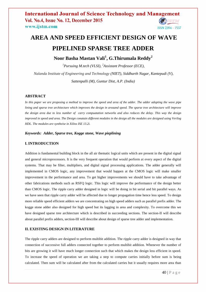
Fig 5.2Technology schematic of the TOP module
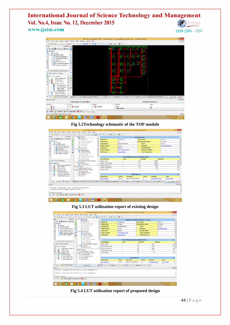
Fig 5.3 LUT utilization report of existing design
Fig 5.4 LUT utilization report of proposed design

45 | P a g e
Fig 5.5 Timing report of Proposed design
Fig 5.6 Timing report of existing design
5.2 Simulation Results
Fig 7.7 Simulated wave forms of Output

46 | P a g e
In this project for simulation we have given inputs like a= 228 and b= 161, output will be as addition we have to
get i.e s= 399. To accomplish addition we need to give ready and clock signal then only addition will be
performed. So we need give clk=rdy=1
VI. CONCLUSION
The sparse tree circuit will reduce the number of carry generation networks present in the parallel prefix adders
such that we employing both techniques in parallel prefix adders. The both mechanism will results in efficient
design in area and speed. The design contain the modules are as Carry merge, carry merge with XOR, buffer
and carry skip adders all are designed using Verilog HDL. To realize the operation of the them we are
synthesized and simulated it. The synthesis process done in Xilinx ISE 13.2 software, this will results in
synthesis report delivers area, speed analysis on Targeted FPGA. The synthesis reports yielding that proposed
design is efficient speed and area.
REFERENCES
[1] Mikhail Dorojevets, Member, IEEE, Christopher L. Ayala, Member, IEEE, Nobuyuki Yoshikawa,
Member, IEEE, and Akira Fujimaki, Member, IEEE “16-Bit Wave-Pipelined Sparse-Tree RSFQ Adder”
[2] P. M. Kogge and H. S. Stone, “A parallel algorithm for the efficient solution of a general class of
recurrence equations,” IEEE Trans. Comput., vol. C-22, no. 8, pp. 786–793, Aug. 1973.
[3] O. A. Mukhanov, S. V. Rylov, V. K. Semonov, and S. V. Vyshenskii, “RSFQ logic arithmetic,” IEEE
Trans. Magn., vol. 25, no. 2, pp. 857–860, Mar. 1989.
[4] Z. J. Deng, N. Yoshikawa, J. A. Tierno, S. R. Whiteley, and T. van Duzer, “Asynchronous circuits and
systems in superconducting RSFQ digital technology,” in Proc. 4th Int. Symp. Adv. Res. Asynchronous
Circuits Syst., Apr. 1998, pp. 274–285 J. Y. Kim, S. Kim, and J. Kang, “Construction of an RSFQ 4-bit
ALU with half adder cells,” IEEE Trans. Appl. Supercond., vol. 15, no. 2, pp. 308– 311, Jun. 2005.
[5] Q. P. Herr, N. Vukovic, C. A. Mancini, K. Gaj, V. Adler, E. G. Friedman, A. Krasniewski, M. F. Bocko,
and M. J. Feldman, “Design and low speed testing of a four-bit RSFQ multiplier-accumulator,” IEEE
Trans. Appl. Supercond., vol. 7, no. 2, pp. 3168–3171, Jun. 1997.
[6] R. Nakamoto, S. Sakuraba, T. Onomi, S. Sato, and K. Nakajima, “4-bit SFQ Multiplier Based on Booth
Encoder,” IEEE Trans. Appl. Supercond., vol. 21, no. 3, pp. 852–855, Jun. 2011.
[7] P. Bunyk and P. Litskevitch, “Case study in RSFQ design: Fast pipelined parallel adder,” IEEE Trans.
Appl. Supercond., vol. 9, no. 2, pp. 3714– 3720, Jun. 1999.
[8] M. Dorojevets, C. L. Ayala, and A. K. Kasperek, “Data-flow microarchitecture for wide datapath RSFQ
processors: Design study,” IEEE Trans. Appl. Supercond., vol. 21, no. 3, pp. 787–791, Jun. 2011.
[9] T. Filippov, M. Dorojevets, A. Sahu, A. Kirichenko, C. Ayala, and O. Mukhanov, “8-bit asynchronous
wave-pipelined RSFQ arithmeticlogic unit,” IEEE Trans. Appl. Supercond., vol. 21, no. 3, pp. 847–851,
Jun. 2011.

47 | P a g e
[10] T. V. Filippov, A. Sahu, A. F. Kirichenko, I. V. Vernik, M. Dorojevets, C. L. Ayala, and O. A.
Mukhanov, “20 GHz operation of an asynchronous wave-pipelined RSFQ arithmetic-logic unit,” Phys.
Proc., vol. 36, pp. 59– 65, 2012
AUTHOR DETAILS
NOOR BASHA MASTAN VALI is pursuing M.tech VLSI system design from Nalanda
Institute of Engineering and Technology. He completed his B.tech. His research of intrest
includes DFTS, VLSI, Low power VLSI design etc.
G.THIRUMALA REDDY is working as assistant professor in Nalanda Institute of
Engineering and Technology. He completed his post graduation in VLSI and his area of
intrest includes analog CMOS,Digital system design, Digital CMOS etc.