architectures and circuits leveraging injection-locked
TRANSCRIPT

Architectures and Circuits Leveraging Injection-Locked
Oscillators for Ultra-Low Voltage Clock Synthesis and
Reference-less Receivers for Dense Chip-to-Chip
Communications
Gautam R. Gangasani
Submitted in partial fulfillment of therequirements for the degree of
Doctor of Philosophyin the Graduate School of Arts and Sciences
COLUMBIA UNIVERSITY2018

c○ 2018
Gautam R. Gangasani
All rights reserved

Architectures and Circuits Leveraging Injection-Locked
Oscillators for Ultra-Low Voltage Clock Synthesis and
Reference-less Receivers for Dense Chip-to-Chip
Communications
Gautam R. Gangasani
Abstract
High performance computing is critical for the needs of scientific discovery and eco-
nomic competitiveness. An extreme-scale computing system at 1000x the performance
of today’s petaflop machines will exhibit massive parallelism on multiple vertical
fronts, from thousands of computational units on a single processor to thousands of
processors in a single data center. To facilitate such a massively-parallel extreme-scale
computing, a key challenge is power. The challenge is not power associated with base
computation but rather the problem of transporting data from one chip to another at
high enough rates. This thesis presents architectures and techniques to achieve low
power and area footprint while achieving high data rates in a dense very-short reach
(VSR) chip-to-chip (C2C) communication network.
High-speed serial communication operating at ultra-low supplies improves the
energy-efficiency and lowers the power envelop of a system doing an exaflop of loops.
One focus area of this thesis is clock synthesis for such energy-efficient interconnect
applications operating at high speeds and ultra-low supplies. A sub-integer clock-
frequency synthesizer is presented that incorporates a multi-phase injection-locked
ring-oscillator-based prescaler for operation at an ultra-low supply voltage of 0.5V,
phase-switching based programmable division for sub-integer clock-frequency synthe-
sis, and automatic calibration to ensure injection lock. A record speed of 9GHz has

been demonstrated at 0.5V in 45nm SOI CMOS. It consumes 3.5mW of power at
9.12GHz and 0.05𝑚𝑚2 of area, while showing an output phase noise of -100dBc/Hz
at 1MHz offset and RMS jitter of 325fs; it achieves a net 𝐹𝑂𝑀𝐴 of -186.5 in a 45-nm
SOI CMOS process.
This thesis also describes a receiver with a reference-less clocking architecture
for high-density VSR-C2C links. This architecture simplifies clock-tree planning in
dense extreme-scaling computing environments and has high-bandwidth CDR to en-
able SSC for suppressing EMI and to mitigate TX jitter requirements. It features
clock-less DFE and a high-bandwidth CDR based on master-slave ILOs for phase
generation/rotation. The RX is implemented in 14nm CMOS and characterized at
19Gb/s. It is 1.5x faster that previous reference-less embedded-oscillator based de-
signs with greater than 100MHz jitter tolerance bandwidth and recovers error-free
data over VSR-C2C channels. It achieves a power-efficiency of 2.9pJ/b while recov-
ering error-free data (BER< 10−12) across a 15dB loss channel. The jitter tolerance
BW of the receiver is > 200MHz and the INL of the ILO-based phase-rotator (32-
Steps/UI) is <1-LSB.
Lastly, this thesis develops a time-domain delay-based modeling of injection lock-
ing to describe injection-locking phenomena in nonharmonic oscillators. The model
is used to predict the locking bandwidth, and the locking dynamics of the locked
oscillator. The model predictions are verified against simulations and measurements
of a four-stage differential ring oscillator. The model is further used to predict the
injection-locking behavior of a single-ended CMOS inverter based ring oscillator, the
lock range of a multi-phase injection-locked ring-oscillator-based prescaler, as well as
the dynamics of tracking injection phase perturbations in injection-locked master-
slave oscillators; demonstrating its versatility in application to any nonharmonic os-
cillator.

Contents
List of Figures iii
List of Tables xi
1 Introduction 1
1.1 Motivation and focus area . . . . . . . . . . . . . . . . . . . . . . . . 1
1.2 Thesis highlights . . . . . . . . . . . . . . . . . . . . . . . . . . . . . 4
1.2.1 Singular performance boost leveraging ILOs . . . . . . . . . . 4
1.2.2 Time-delay based model for nonharmonic ILOs . . . . . . . . 7
1.2.3 A 0.5V, 9GHz Sub-Integer Clock-Frequency Synthesizer using
Multi-Phase Injection-Locked Prescaler . . . . . . . . . . . . . 7
1.2.4 RX for VSR C2C links with Clock-less DFE and high band-
width CDR . . . . . . . . . . . . . . . . . . . . . . . . . . . . 8
1.3 Thesis Organization . . . . . . . . . . . . . . . . . . . . . . . . . . . . 10
2 Time-Domain Model for Injection Locking in Nonharmonic Oscilla-
tors 11
2.1 Introduction . . . . . . . . . . . . . . . . . . . . . . . . . . . . . . . . 11
2.2 Models for Injection Locking . . . . . . . . . . . . . . . . . . . . . . . 12
2.3 Quasi-Linear Model For Injection Locking in Differential Ring Oscillators 15
2.4 Time-Domain Model For Injection Locking in Differential Ring Oscil-
lators . . . . . . . . . . . . . . . . . . . . . . . . . . . . . . . . . . . . 20
2.4.1 Analytical Expressions for the Oscillator Waveforms . . . . . . 20
i

2.4.2 Effect of an Injection Signal . . . . . . . . . . . . . . . . . . . 22
2.4.3 Injection Locking Range . . . . . . . . . . . . . . . . . . . . . 23
2.4.4 Injection Locking Dynamics . . . . . . . . . . . . . . . . . . . 27
2.5 Time-Domain Model For Injection Locking in Single-Ended Inverter
Based Ring Oscillator . . . . . . . . . . . . . . . . . . . . . . . . . . . 31
2.5.1 d vs. Δ Relationship . . . . . . . . . . . . . . . . . . . . . . . 32
2.5.2 Injection Locking Range . . . . . . . . . . . . . . . . . . . . . 34
2.5.3 Injection Locking Dynamics . . . . . . . . . . . . . . . . . . . 37
2.6 Summary . . . . . . . . . . . . . . . . . . . . . . . . . . . . . . . . . 39
3 A 9GHz Sub-Integer Clock-Frequency Synthesizer at Ultra-Low Sup-
ply 40
3.1 Introduction . . . . . . . . . . . . . . . . . . . . . . . . . . . . . . . . 40
3.2 Architecture and circuit description . . . . . . . . . . . . . . . . . . . 42
3.2.1 PFD, CP, and VCO . . . . . . . . . . . . . . . . . . . . . . . 42
3.2.2 ILRO based Prescaler . . . . . . . . . . . . . . . . . . . . . . . 44
3.2.3 Phase-Switching Programmable Divider . . . . . . . . . . . . 48
3.2.4 Automatic Injection-Lock Calibration . . . . . . . . . . . . . . 49
3.3 Experimental Results . . . . . . . . . . . . . . . . . . . . . . . . . . . 51
3.4 Summary . . . . . . . . . . . . . . . . . . . . . . . . . . . . . . . . . 57
4 A 19Gb/s Receiver for Chip-to-Chip Links with Clock-Less DFE
and High-BW CDR based on Master-Slave ILOs 59
4.1 Introduction . . . . . . . . . . . . . . . . . . . . . . . . . . . . . . . . 59
4.2 System-level Considerations . . . . . . . . . . . . . . . . . . . . . . . 61
4.2.1 Channel Equalization . . . . . . . . . . . . . . . . . . . . . . . 61
4.2.2 Receiver Architecture . . . . . . . . . . . . . . . . . . . . . . . 63
4.3 Circuit Blocks and Descriptions . . . . . . . . . . . . . . . . . . . . . 67
4.3.1 CTLE . . . . . . . . . . . . . . . . . . . . . . . . . . . . . . . 67
4.3.2 Data Edge-Detection and Injection . . . . . . . . . . . . . . . 67
4.3.3 Reference-less frequency acquisition . . . . . . . . . . . . . . . 71
ii

4.3.4 Resistively-Interpolated MILO-SILO based Phase-Rotation . . 75
4.3.5 Clock-less DFE . . . . . . . . . . . . . . . . . . . . . . . . . . 78
4.3.6 Jitter-tolerance BW using 𝑑 vs. Δ based time-delay model . . 82
4.4 Measurements . . . . . . . . . . . . . . . . . . . . . . . . . . . . . . . 85
4.4.1 Experimental Setups . . . . . . . . . . . . . . . . . . . . . . . 85
4.4.2 MILO-SILO, Phase Rotation and Recovered Clock . . . . . . 85
4.4.3 Receiver Performance . . . . . . . . . . . . . . . . . . . . . . . 90
4.4.4 Performance summary and comparison . . . . . . . . . . . . . 96
4.5 Summary . . . . . . . . . . . . . . . . . . . . . . . . . . . . . . . . . 99
5 Conclusion 100
5.1 Future Research . . . . . . . . . . . . . . . . . . . . . . . . . . . . . . 102
Bibliography 103
iii

List of Figures
1-1 Exascale performance needs to rely on massive parallelism. . . . . . . 2
1-2 A strawman architecture for a massively-parallel exascale processor
running a billion parallel threads. Reprinted from [4]. . . . . . . . . . 3
1-3 Prior-art of various applications leveraging ILOs. . . . . . . . . . . . 5
1-4 Singular performance boost, such as highest reported clock-frequency
synthesizer speed at ultra-low supply of 0.5V and highest reported
chip-to-chip operation for links with > 100𝑀𝐻𝑧 CDR bandwidth, is
reported when leveraging unique features of ILOs. . . . . . . . . . . . 6
1-5 Block diagram of the ultra-low supply clock-frequency synthesizer. . . 8
1-6 Quarter-rate RX architecture for very short-reach chip-to-chip links
with clock-less DFE and high-bandwidth CDR based on Master-Slave
injection-locked oscillators. . . . . . . . . . . . . . . . . . . . . . . . . 9
2-1 (a) Frequency domain model for injection locking of resonator based
oscillators; (b) Resonator amplitude and phase characteristic; the am-
plifier 𝐴 is assumed to have a unity frequency response; (c) phasor
diagram at 𝜔INJ for the signals in the locked oscillator when in steady
state. . . . . . . . . . . . . . . . . . . . . . . . . . . . . . . . . . . . . 13
iv

2-2 (a) Delay based, time-domain model for injection locking in non-harmonic
oscillators; the delay element, 𝐷, has a delay 𝑇𝑑 whereas the inverter
is assumed ideal with zero delay; (b) the free-running frequency of os-
cillation, 𝑓0, is 1/(2𝑇𝑑); (c) assuming finite transition-slope signals, the
addition of an injection signal, 𝑆INJ , to the oscillator signal, 𝑆𝐼 , re-
sults in an extra delay, 𝑑, in the oscillation loop so that 𝑓𝑜𝑠𝑐 = 𝑓𝐼𝑁𝐽 =
1/(2(𝑇𝑑 + 𝑑)) in the injection-locked state. . . . . . . . . . . . . . . . 14
2-3 Four stage differential ring oscillator, with an injection stage operating
on the the first stage. The oscillator’s delay stages (1-4) are identical;
the injection stage’s bias current and degeneration resistance are scaled
to scale the injection level. . . . . . . . . . . . . . . . . . . . . . . . . 16
2-4 Edges of the locking range for the differential 4-stage ring oscillator
operating quasi linearly w.r.t. the ratio 𝛼 . . . . . . . . . . . . . . . . 17
2-5 𝜃 w.r.t. the injection frequency for the differential 4-stage ring oscillator
operating quasi-linearly with 𝛼 = 10. . . . . . . . . . . . . . . . . . . 18
2-6 Measured waveforms for the differential 4-stage ring oscillator oper-
ating quasi-linearly (𝑅𝐸 = 20 Ω): injection input 𝑉𝑖𝑛𝑗, stage 1 input
𝑉𝑖1 and stage 1 output 𝑉𝑂1 with 𝛼 = 10; (top) 𝑉𝑖𝑛𝑗 is −99.84𝑜 out
of phase with 𝑉𝑖1 at 3.375 MHz, the upper edge of the locking band-
width; (middle) 𝑉𝑖𝑛𝑗 is in phase with 𝑉𝑖1 in the center of the lock range
at 3.21 MHz; (bottom) 𝑉𝑖𝑛𝑗 is 79.75𝑜 out of phase with the oscillat-
ing input waveform 𝑉𝑖1, at 3.098 MHz, the lower edge of the locking
bandwidth. . . . . . . . . . . . . . . . . . . . . . . . . . . . . . . . . 19
2-7 For non-linear operation each stage of Fig. 2-3 is modeled as a hard
amplitude limiting mechanism, whose output current drives a 𝑅-𝐶 load. 21
2-8 Differential output voltage 𝑣𝑑(𝑡) of a stage in the 4-stage ring-oscillator
of Fig. 2-3. . . . . . . . . . . . . . . . . . . . . . . . . . . . . . . . . . 21
2-9 Effect of the injection signal on the output voltage 𝑣𝑑 = 𝑣𝑑,𝑖 + 𝑣𝑑,𝑖𝑛𝑗 . 22
v

2-10 Waveforms for the differential 4-stage ring oscillator when injection
locked; the last 3 stages have a delay 𝑡𝑑 and the first stage has a delay
𝑡𝑑 + 𝑑 due to the injection. . . . . . . . . . . . . . . . . . . . . . . . . 24
2-11 Measured waveforms for the differential 4-stage ring oscillator operat-
ing non linearly (𝑅𝐸 = 0 Ω) with 𝛼 = 10: the injected signal, 𝑉𝑖𝑛𝑗,
the stage 1 input voltage, 𝑉𝐼1, and the stage 1 output voltage, 𝑉𝑂1, are
shown for varying Δ, the delay between 𝑉𝐼𝑁𝐽 and 𝑉𝐼1; (top) Δ = Δ𝑚𝑖𝑛
at the upper edge of lock range at 3.61 MHz; 𝑡𝑑1, the delay through
stage 1, i.e. the delay between 𝑉𝑂1 and 𝑉𝐼1, is 31.4 ns; Δ = 0 and
𝑡𝑑1 = 36.1 ns in the middle of the lock range at 3.49 MHz; (bottom)
Δ = Δ𝑚𝑎𝑥 and 𝑡𝑑1 = 39.1 ns at the lower edge of the lock range at
3.37 MHz. . . . . . . . . . . . . . . . . . . . . . . . . . . . . . . . . . 25
2-12 Edges of the locking range w.r.t. 𝛼 for the differential 4-stage ring
oscillator operating non linearly . . . . . . . . . . . . . . . . . . . . . 26
2-13 Calculated, simulated and measured 𝑑 as a function of Δ for the dif-
ferential 4-stage ring oscillator operating non-linearly with (a) 𝛼 = 10
and (b) 𝛼 = 6.8. . . . . . . . . . . . . . . . . . . . . . . . . . . . . . . 27
2-14 Injection lock transient waveforms for the differential 4-stage ring os-
cillator used for the derivation of Δ[𝑛+ 1] from Δ[𝑛]. . . . . . . . . . 28
2-15 Simulated and calculated injection lock dynamics of the differential
4-stage ring oscillator for a step change in frequency from 3.4MHz to
3.6MHz at 𝛼 = 10 (top) 𝛼 = 6.8 (bottom). . . . . . . . . . . . . . . . 29
2-16 Experimental setup used to observe the injection lock dynamics of the
4-stage differential ring oscillator. . . . . . . . . . . . . . . . . . . . . 30
2-17 After an FM modulation step trigger, the injection frequency generator
settled to the new frequency in about 1.5 cycles; that time point is
labeled as 𝑇 = 0. . . . . . . . . . . . . . . . . . . . . . . . . . . . . . 30
2-18 Measured and calculated injection lock dynamics of the 4-stage differ-
ential ring oscillators for a step change in frequency from 3.4MHz to
3.6MHz at 𝛼 = 10 (top) 𝛼 = 6.8 (bottom). . . . . . . . . . . . . . . . 31
vi

2-19 Single-ended 3-stage CMOS-inverter based ring oscillator, with an in-
jection stage operating on the the first stage. Each of the three stages is
made of nine (9x) identical inverters. For closed-loop operation switch
S1 is closed. The injection level can be switched from 𝛼 = 9 to 𝛼 = 4.5
by opening or closing switches (S2,S3). . . . . . . . . . . . . . . . . . 32
2-20 Waveforms and the definition of d and Δ for the single-ended 3-stage
ring oscillator in Fig. 2-19. . . . . . . . . . . . . . . . . . . . . . . . . 33
2-21 d vs. Δ relationship for the single-ended 3-stage ring oscillator obtained
through open-loop simulations for different values of 𝛼. Also shown are
the 𝑑 vs. Δ relationships when the oscillator is operating in closed loop
and injection locked. . . . . . . . . . . . . . . . . . . . . . . . . . . . 34
2-22 Open-loop d vs. Δ plots obtained through measurements and simula-
tions at 𝛼 = 9 for the single-ended 3-stage ring oscillator. . . . . . . . 35
2-23 Open-loop d vs. Δ plots obtained through measurements and simula-
tions at 𝛼 = 4.5 for the single-ended 3-stage ring oscillator. . . . . . . 35
2-24 Closed-loop d vs. Δ plots obtained through measurements and simu-
lations for the single-ended 3-stage ring oscillator. . . . . . . . . . . . 36
2-25 Edges of the locking range w.r.t. 𝛼 for the single-ended 3-stage ring
oscillator . . . . . . . . . . . . . . . . . . . . . . . . . . . . . . . . . . 36
2-26 Measured and calculated injection lock dynamics for the single-ended
3-stage ring oscillator for a step change in frequency from 9.35MHz to
9.75MHz at (top) 𝛼 = 9 (bottom) 𝛼 = 4.5. . . . . . . . . . . . . . . . 38
2-27 Simulated and calculated injection lock dynamics for the single-ended
3-stage ring oscillator for a step change in frequency from 9.35MHz to
9.75MHz at (top) 𝛼 = 9 (bottom) 𝛼 = 4.5. . . . . . . . . . . . . . . . 38
3-1 Block diagram of the ultra-low supply sub-integer clock-frequency syn-
thesizer using ILRO based prescaler for divide-by-3 function, followed
by a phase-switching based sub-integer programmable divider and an
automatic injection-lock calibration loop for ILRO and VCO. . . . . . 41
vii
3-2 PFD with extra delay in reset path. . . . . . . . . . . . . . . . . . . . 43
3-3 Differential charge-pump with unity-gain buffer based architecture along
with common-mode feedback circuit. . . . . . . . . . . . . . . . . . . 43
3-4 VCO, using a cross-coupled inverter architecture. . . . . . . . . . . . 45
3-5 General concept of odd-M stage multi-input injection to achieve modulo-
M division and achieve wider injection lock range. . . . . . . . . . . . 46
3-6 Ultra-low voltage pseudo-differential implementation of the ILRO prescaler
in a divide-by-3 configuration. . . . . . . . . . . . . . . . . . . . . . . 47
3-7 Circuit block diagram for the phase-switching based programmable
divider. . . . . . . . . . . . . . . . . . . . . . . . . . . . . . . . . . . 48
3-8 Automatic injection-lock calibration algorithm to coarsely set the ILRO
free-running frequency. . . . . . . . . . . . . . . . . . . . . . . . . . . 49
3-9 Automatic injection-lock calibration algorithm to optimally select the
VCO band. . . . . . . . . . . . . . . . . . . . . . . . . . . . . . . . . 50
3-10 Fabricated chip micrograph and layout of the PLL. . . . . . . . . . . 51
3-11 Measurement of (a)𝑉𝑐𝑖𝑙𝑜 versus 𝐹𝑜𝑠𝑐 (b) Input dBm versus Freq. lock
range. . . . . . . . . . . . . . . . . . . . . . . . . . . . . . . . . . . . 52
3-12 Linear-fit of measured and calculated lock ranges at different injection
input levels and self-oscillation frequencies. . . . . . . . . . . . . . . . 53
3-13 (a)Vco gain curves. (b) Auto-calibration between ILRO and VCO. . . 54
3-14 Measurement of (a) Output spectra of the clock-frequency synthesizer
at different sub-integer division ratios. (b) Phase noise plot at division
ratio of 96. . . . . . . . . . . . . . . . . . . . . . . . . . . . . . . . . . 56
3-15 Power consumption distribution in the sub-integer clock-frequency syn-
thesizer. . . . . . . . . . . . . . . . . . . . . . . . . . . . . . . . . . . 57
4-1 RX equalization capabilities, such as CTLE peaking and 1-tap DFE
are evaluated for channel performance margins. . . . . . . . . . . . . 63
viii

4-2 Channel operating margin study with signal impairments at different
RX peaking and DFE settings. 1-tap DFE gives robustness to system
solution in case of degradation due to crosstalk and PN-skew. To im-
prove signal-to-noise ratio in face of crosstalk, peaking could be dialed
down and ℎ1-tap could be used for post-cursor equalization. . . . . . 65
4-3 Quarter-rate RX architecture for very short-reach chip-to-chip links
with clock-less DFE and high-bandwidth CDR based on Master-Slave
injection-locked oscillators. . . . . . . . . . . . . . . . . . . . . . . . . 66
4-4 RX CTLE equalization using a single-stage peaking amplifier. . . . . 68
4-5 Power spectrum of NRZ signalling for a L-bit repeating pattern, show-
ing a null at data rate. . . . . . . . . . . . . . . . . . . . . . . . . . . 69
4-6 (a) RZ data spectra with 𝑇𝑏/2 delay into the XOR cell (b) Simulated
RZ injection level with 19Gbps NRZ input data rate. . . . . . . . . . 70
4-7 Edge-detection, clock signal extraction and injection scheme. . . . . . 71
4-8 Schematics of limiting-amplifier used for ∼20dB differential gain. . . . 71
4-9 (a) The replica delay-line uses the regulated-voltage of the MILO-SILO
block as well as the 𝐶𝐿 settings to track the data rate by maintaining
𝑇𝑏/2 delay (b) Simulated tracking variation due to mismatch in the
replica buffer. . . . . . . . . . . . . . . . . . . . . . . . . . . . . . . . 72
4-10 Schematics of CML XOR stage. . . . . . . . . . . . . . . . . . . . . . 73
4-11 Shows the use of consecutive early-late transitions to discriminate be-
tween and phase and frequency error for tracking and correction. . . . 76
4-12 Reference-less frequency lock algorithm which sets the MILO-SILO free
running frequency to lock in the center of the injection lock range. This
ensures optimal margin against drift and for jitter-tolerance. . . . . . 77
4-13 Master-Slave ILO-based 360𝑜 phase-rotation using resistive-interpolated
edges for injection. . . . . . . . . . . . . . . . . . . . . . . . . . . . . 79
4-14 Coarse phase-selections to fine resistive-interpolation settings at differ-
ent phase-rotator positions over 2UI. . . . . . . . . . . . . . . . . . . 80
ix
4-15 Clock-less direct-feedback DFE with variable delay replica-cell tied to
the delay elements in ILOs to optimally meet DFE loop timing margins. 81
4-16 Discrete-time model of the dual-loop clock-data recovery loop. . . . . 83
4-17 Relationship between input injection phase perturbation and output
phase change and its impact on settling time constant. . . . . . . . . 83
4-18 Open-loop 𝑑 vs. Δ values of MILO-SILO used to calculate JTOL and
compared against closed-loop simulations. . . . . . . . . . . . . . . . 84
4-19 Fabricated chip micrograph and layout. . . . . . . . . . . . . . . . . . 86
4-20 Measurement setup of the DUT. Data is generated in J-BERT N4903B
and multiplied up using N4876A 2:1 multiplexer. The data then goes
through a Megtron6 PCB before entering the DUT on the probe sta-
tion. Serial-scan interface is controlled using National Instruments
NI-2162 digital I/O accessory and NI PXI-1042, which is also used to
interface with LabView GUI. . . . . . . . . . . . . . . . . . . . . . . . 87
4-21 Shows the setup used to measure the rotator INL/DNL. 1010 data
pattern from the J-Bert is multiplied up using N4870A 2:1 Mux to
injection-lock into the MILO-SILO in the device under test (D.U.T).
The MILO-SILO phase-rotator output recovered clock from D.U.T is
pattern-locked to a trigger in DCA-X 86100D sampling scope. MILO-
SILO phase-rotator is rotated and its phase-step is calculated with
reference to the previous waveform in scope memory. . . . . . . . . . 88
4-22 Lock range of MILO-SILO at different frequency control voltages (𝑣𝑐)
and switchable load cap (𝐶𝐿) with (a)1010 pattern. (b) PRBS7 pattern. 89
4-23 Measured INL/DNL values of the MILO-SILO based phase-rotator
over extremes of operating speed. . . . . . . . . . . . . . . . . . . . . 90
4-24 Measurement of random jitter (𝑅𝐽𝑟𝑚𝑠) on the recovered clock includes
not only the jitter transfer from the injected data but also the output
clock buffers and driver. . . . . . . . . . . . . . . . . . . . . . . . . . 91
x
4-25 (a) Recovered clock random jitter as function of data baudrate post-
BBFD (b) After initial frequency lock calibration, as supply voltage of
the MILO-SILO regulator changes by ±5% or as temperature deviates
between 0C and 100C, the recovered clock RJ shows less than 10fs of
deviation with no discernible trends. . . . . . . . . . . . . . . . . . . 92
4-26 Measured channel insertion loss over 20-inch Megtron6 PCB and𝑅𝑥𝐼𝑛𝑝𝑢𝑡
eye diagram after channel at 19Gb/s. . . . . . . . . . . . . . . . . . . 93
4-27 RX performance at 19Gbps over 20-inch MEG6 channel. . . . . . . . 94
4-28 (a)Measured JTOL BW at 19Gb/s for PRBS7 data at BER of 10−12
over a 10dB loss channel (b) JTOL BW as a funtion of temperature
variation after frequency lock calibration. . . . . . . . . . . . . . . . . 95
4-29 Power consumption distribution in the RX. . . . . . . . . . . . . . . . 97
4-30 Comparison of RX CDR bandwidth, speed, power efficiency, and chan-
nel loss at Nyquist against other reference-less clock-data recovery de-
signs. . . . . . . . . . . . . . . . . . . . . . . . . . . . . . . . . . . . . 98
xi

List of Tables
2.1 Lock range measurements and predictions for the 4-stage differential
ring oscillator operating non linearly . . . . . . . . . . . . . . . . . . 26
2.2 Lock range predictions, measurements, and simulations for the single-
ended 3-stage ring oscillator . . . . . . . . . . . . . . . . . . . . . . . 37
3.1 Performance Summary and Comparison of Low-Supply PLLs. . . . . 55
4.1 Shows the many parameters used for channel margin study . . . . . . 62
4.2 Summary of receiver performance. . . . . . . . . . . . . . . . . . . . . 96
4.3 State of art comparison of energy-efficient dense VSR-C2C interconnects 98
xii

Acknowledgements
I would especially like to thank my Ph.D. advisor, Prof. Kinget, whose support and
guidance made this work possible. His approach to research, from defining the prob-
lem in the broader context to approaching it from innovative angles while maintaining
clarity, is inspiring and hopefully I have learnt some of it to carry forward. I also wish
to acknowledge Prof. Tsividis and Prof. Shepard at Columbia for teaching some of
the best courses I ever had, these courses gave me a solid foundation in integrated
circuit design. This work would not have been possible without material support and
encouragement from my managers at IBM and at Globalfoundries, Kevin Kramer and
Daniel Storaska. My deepest appreciation to them for showing faith in me through
the years. Over the years I have had the pleasure of working with many talented
individuals, some of my best learning, insights and successes were possible through
this teamwork. I would especially like to acknowledge the collegial camaraderie I have
enjoyed while working with Dr. Bulzacchelli, Dr. Meghelli, and Dr. C.-M. Hsu. Next
I wish to thank all the people who helped me build the prototypes and test the chips,
some of whom are: Kevin Guay, George May, Al Brouillette, Ruben Recinos, Peter
Coutu, and Mike Wielgos. Finally, I wish to offer my sincere gratitude to my friends
and family, who have been instrumental in my life not only in influencing me but also
supporting me to complete this degree. I thank my entire family: my parents, sister
and brother-in-law, parents-in-law and every one else who has offered me so much
support. I thank my lovely kids, Pallavi and Nikhil, for their love and for giving me
a deeper perspective and the pleasure of leading a fuller life. And lastly, I offer my
dearest thanks to my wife, Veena, without whose super mom like abilities, in running
a busy medical practice and a household through my unpredictable schedules, nothing
would have been possible. I owe an eternal debt to her love, support, and kindness
through it all.
xiii
Chapter 1
Introduction
1.1 Motivation and focus area
In high-performance computing (HPC), the major milestones are emergence of sys-
tems whose aggregate performance first crosses a threshold of 103𝑘 operations per-
formed per second, for some k. Gigascale (109) was achieved in 1985, terascale (1012)
was achieved in 1997. Today there are petascale (1015) systems deployed, and exascale
(1018) systems is the next way point in HPC. Scientific frontiers demand faster and
bigger computers to analyze an avalanche of data and advance our knowledge. A quest
for answers to grand scientific challenges is the main motivation behind developing
and building exascale supercomputers and beyond [1].
The semiconductor industry has been fueled by systems utilizing continuous im-
provement in the cost, performance, and power of semiconductor content. Historically
these improvements have delivered the resultant Dennard scaling benefits in power
and performance. These improved metrics translated in a straight forward manner
from device to circuit to processors to systems. Moore’s law scaling, interpreted with
the paradigm above, is finished; and there are increasingly difficult challenges in de-
livering power/performance/cost improvements at device level to circuits and system
level [2].
To achieve exascale operation, rather than Moore’s law one has to rely on massive
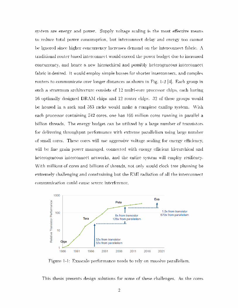
parallelism as shown in Fig. 1-1 [3]. The key challenges to a massively-parallel exascale
1
system are energy and power. Supply voltage scaling is the most effective means
to reduce total power consumption, but interconnect delay and energy too cannot
be ignored since higher concurrency increases demand on the interconnect fabric. A
traditional router based interconnect would exceed the power budget due to increased
concurrency, and hence a new hierarchical and possibly heterogeneous interconnect
fabric is desired. It would employ simple busses for shorter interconnect, and complex
routers to communicate over longer distances as shown in Fig. 1-2 [4]. Each group in
such a strawman architecture consists of 12 multi-core processor chips, each having
16 optimally designed DRAM chips and 12 router chips. 32 of these groups would
be housed in a rack and 583 racks would make a complete exaflop system. With
each processor containing 742 cores, one has 166 million cores running in parallel a
billion threads. The energy budget can be utilized by a large number of transistors
for delivering throughput performance with extreme parallelism using large number
of small cores. These cores will use aggressive voltage scaling for energy efficiency,
will be fine grain power managed, connected with energy efficient hierarchical and
heterogeneous interconnect networks, and the entire system will employ resiliency.
With millions of cores and billions of threads, not only would clock tree planning be
extremely challenging and constraining but the EMI radiation of all the interconnect
communication could cause severe interference.
Figure 1-1: Exascale performance needs to rely on massive parallelism.
This thesis presents design solutions for some of these challenges. As the cores
2
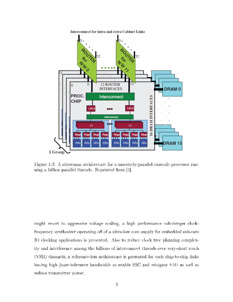
Figure 1-2: A strawman architecture for a massively-parallel exascale processor run-ning a billion parallel threads. Reprinted from [4].
might resort to aggressive voltage scaling, a high performance sub-integer clock-
frequency synthesizer operating off of a ultra-low core supply for embedded sub-rate
IO clocking applications is presented. Also to reduce clock tree planning complex-
ity and interference among the billions of interconnect threads over very-short reach
(VSR) channels, a reference-less architecture is presented for such chip-to-chip links
having high jitter-tolerance bandwidth to enable SSC and mitigate EMI as well as
reduce transmitter power.
3

1.2 Thesis highlights
1.2.1 Singular performance boost leveraging ILOs
An oscillator can be pulled in to an injected signal frequency if periodic steady-state
injection leads to a change in the average period of the oscillator. The constraint of
periodicity in the steady-state behavior along with strength of injection limits the lock
range. Also, the synchronization effect of injection manifests itself as correction of the
oscillator zero crossings. A resultant reduction of phase noise depends on injection
level, initial frequency delta and the number of oscillator periods of jitter accumulation
between periodic injection pulses. A combination of these basic principles manifest
themselves in many of today’s transceiver and frequency synthesis techniques, as seen
in Fig. 1-3.
Superharmonic ILOs achieve even/odd division at very high operating speeds
[5–12]. While, subharmonic ILOs achieve frequency multiplication with multi-phase
outputs [13–17]. Delay modulation between master and slave ILOs leads to 360𝑜
phase-rotation with jitter-filtering [18]. A grid of coupled ILOs is shown to produce
a standing-wave oscillator for reduced clock skew across the chip [19]. Forwarded-
clock injection-locked to local oscillators aids clock-data recovery without a PLL or
a full-fledged CDR with good jitter-tolerance bandwidth and low power [20–23]. A
popular technique is to inject a subharmonic reference clock into the oscillator in a
PLL to lower the phase noise [24–38]. High bandwidth CDR and burst-mode oper-
ation is possible by injection locking the data edges into the oscillator for recovered
clock [39–41]. ILO when used as a prescaler increase the speed of operation [42, 43].
Injection-lock based carrier synchronization is demonstrated in a mm-wave intra-
connect solution [44]. Finally, fast settling of an ILO is used to modulate a transmitter
for direct FSK modulation [45].
Fig. 1-4, shows the record performances demonstrated in this thesis leveraging
low-supply operation of injection-locked oscillators at high relative speeds and high-
bandwidth of the locking process of the ILOs to track input jitter on the injected
signal. The subsequent sub-sections highlight these features.
4

Leveraging
ILOs
Superharmonic
injection
Injection-
locked
phase-
rotationStanding
wave
oscillator
Subharmonic
injection
Forwarded-
clock
injection
Subharmonic-
injection
locked PLL
Data-
injection
burst-mode
CDR
Injection-
locked
prescalerInjection-
locked
wireless
intra-connect
Injection-
locked
FSK
modulation
Figure 1-3: Prior-art of various applications leveraging ILOs.
5

Singular
Performance-boost
Leveraging
Non-harmonic
ILOs
Lock-range
and BW
>200MHz
CDR-BW
Highest speed
C2C link
Low-headroom
operation
0.5V supply
Highest speed
Sub-Integer
Clock synth.
Non-harmonic
signals
First of
its kind
Time-delay
based model
Figure 1-4: Singular performance boost, such as highest reported clock-frequencysynthesizer speed at ultra-low supply of 0.5V and highest reported chip-to-chip oper-ation for links with > 100𝑀𝐻𝑧 CDR bandwidth, is reported when leveraging uniquefeatures of ILOs.
6

1.2.2 Time-delay based model for nonharmonic ILOs
A time-domain delay-based model was developed to predict the injection locking be-
havior of non-harmonic oscillators such as ring oscillators. The effect of the injection
signal on the oscillator is modeled with a d versus Δ characteristic which captures
the additional delay d in a stage due to the effect of the injection signal with a delay
Δ. Using this characteristic, the injection-locking range as well as injection-locking
dynamics can be accurately modeled and predicted. This modeling approach was
applied to a differential four-stage ring oscillator where analytical expressions for the
waveforms could be derived along with an analytical expression for the d versus Δ
characteristic. Versatility of the modeling approach was demonstrated by analyzing
the locking behavior of a single-ended three-stage CMOS-inverter-based ring oscilla-
tor. In this case the d versus Δ characteristic was derived from simulations and mea-
surements. By simulating for d versus Δ characteristic, the model is also applied to
predict the lock range of a multi-phase injection-locked ring-oscillator-based prescaler,
as well as the dynamics of tracking injection phase perturbations in injection-locked
master-slave oscillators. The presented time-domain delay-based modeling approach
can be applied to any nonharmonic oscillator as long as the relationship between the
extra delay, d, and the delay, Δ, between the injection signal and the relevant internal
oscillator is available.
1.2.3 A 0.5V, 9GHz Sub-Integer Clock-Frequency Synthesizer
using Multi-Phase Injection-Locked Prescaler
A 9-GHz sub-integer clock-frequency synthesizer, shown in Fig. 1-5, incorporates a
multi-phase injection-locked ring-oscillator-based prescaler for operation at an ultra-
low supply voltage of 0.5V, phase-switching based programmable division for sub-
integer clock-frequency synthesis, and automatic calibration to ensure injection lock.
The synthesizer consumes 3.5mW of power at 9.12GHz and 0.05mm2 of area, while
showing an output phase noise of -100dBc/Hz at 1MHz offset and RMS jitter of 325fs;
it achieves a net FOM𝐴 of -186.5 in a 45-nm SOI CMOS process. Key features are:
7

PFD CP LPF VCO
2:1MUX
PrescalerILRO/3
ProgrammableSub-IntegerDivider
FrequencyCounter
Off-chip Controller
/D:(96,96.5,97,97.5,98,98.5)
𝐹𝑟𝑒𝑓
𝑉𝑐𝑝
𝐹𝑣𝑐𝑜
𝐹𝑓𝑏𝑐𝑙𝑘
𝑉𝑐𝑖𝑙𝑜
𝑏<𝑖>
𝐹𝑖𝑛
𝐶0
𝐹𝐶
𝐶60
𝐶120
𝐹𝑖𝑛𝑗
Figure 1-5: Block diagram of the ultra-low supply clock-frequency synthesizer.
(a) A record speed of 9GHz has been demonstrated at 0.5V in 45nm SOI CMOS.
(b) The proposed multi-phase multi-input ILRO-prescaler eliminates the speed bot-
tleneck, while automatic injection-lock calibration ensures lock between the VCO
and the ILRO-prescaler.
(c) The phase-switching based programmable divider structure provides fine fre-
quency resolution through sub-integer division.
1.2.4 RX for VSR C2C links with Clock-less DFE and high
bandwidth CDR
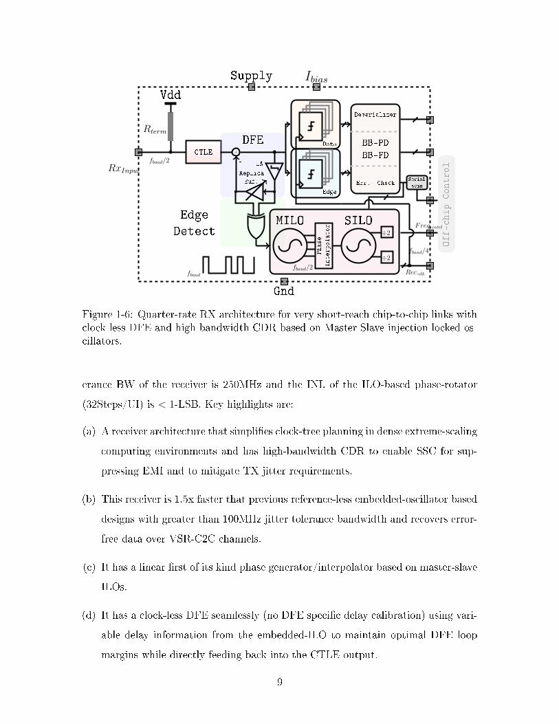
A RX with a reference-less clocking architecture, Fig. 1-6, for high-density VSR-C2C
links is described. It features clock-less DFE and a high-bandwidth CDR based on
master-slave ILOs for phase generation/rotation. The RX is implemented in 14nm
CMOS and characterized at 19Gb/s. It achieves a power-efficiency of 2.9pJ/b while
recovering error-free data (BER< 10−12) across a 15dB loss channel. The jitter tol-
8
𝑅𝑥𝐼𝑛𝑝𝑢𝑡
Supply 𝐼𝑏𝑖𝑎𝑠
Off-chipControl
Gnd
Vdd
𝑅𝑡𝑒𝑟𝑚
𝑓𝑏𝑎𝑢𝑑/2CTLE
BB-PD
BB-FD
Deserializer
Err. Check
+
DFE
LA
Replica
Buf.
-
Edge
Detect
𝑓𝑏𝑎𝑢𝑑
MILO SILO
Phase
Interpolator
÷2
÷2
𝑓𝑏𝑎𝑢𝑑/2
Serial
scan
Data
Edge
𝐹𝑟𝑒𝑞.𝑐𝑛𝑡𝑟𝑙
𝑓𝑏𝑎𝑢𝑑/4
𝑅𝑒𝑐.𝑐𝑙𝑘
Figure 1-6: Quarter-rate RX architecture for very short-reach chip-to-chip links withclock-less DFE and high-bandwidth CDR based on Master-Slave injection-locked os-cillators.
erance BW of the receiver is 250MHz and the INL of the ILO-based phase-rotator
(32Steps/UI) is < 1-LSB. Key highlights are:
(a) A receiver architecture that simplifies clock-tree planning in dense extreme-scaling
computing environments and has high-bandwidth CDR to enable SSC for sup-
pressing EMI and to mitigate TX jitter requirements.
(b) This receiver is 1.5x faster that previous reference-less embedded-oscillator based
designs with greater than 100MHz jitter tolerance bandwidth and recovers error-
free data over VSR-C2C channels.
(c) It has a linear first of its kind phase generator/interpolator based on master-slave
ILOs.
(d) It has a clock-less DFE seamlessly (no DFE specific delay calibration) using vari-
able delay information from the embedded-ILO to maintain optimal DFE loop
margins while directly feeding back into the CTLE output.
9

1.3 Thesis Organization
This thesis focuses on presenting the advances in circuits and systems for serial com-
munications in extreme-scale systems and some of the relevant modeling. Injection-
locked oscillators are heavily leveraged to achieve high speed and performance at
ultra-low scaled core supplies and to achieve high-bandwidth clock-data recovery us-
ing embedded reference-less oscillators. Chapter 2 takes a unique and essentially sim-
plifying perspective on non-harmonic ILOs and develops a time-delay based model to
predict any ILOs locking range and dynamics. The model is developed based on the
correlation between the delay of the injected signal w.r.t. the oscillator signal into a
stage and its effect on the output delay of that oscillator stage.
Chapter 3 focuses on high-performance clock synthesis based off likely ultra-low
scaled core supply in extremely-scale systems. It uses a minimal stack to have the
highest possible speed for the injection-locked prescaler, a key speed bottleneck. Im-
portant techniques to automatically achieve lock between the VCO and prescaler as
well as achieving programmable sub-integer division without compromising the loop
bandwidth are presented. Such a technique would be of interest when an embed-
ded sub-rate clocking is needed to work off the core supply with small power/area
signature.
Chapter 4 follows with a solution for potential issue of clock-tree planning and in-
terference in extreme-scale system with billons of threads. It presents a reference-less
RX for VSR chip-to-chip links which mitigates the complexity of clock-tree planning
and improves resilience of the system. Also, the high bandwidth of the clock-data
recovery lends the design to SSC and improved EMI and potential TX power savings
due to reduced jitter requirements. Finally, chapter 5 summarizes the thesis and ends
with a discussion of potential avenues for future research.
10

Chapter 2
Time-Domain Model for Injection
Locking in Nonharmonic Oscillators
2.1 Introduction
Injecting a signal into an oscillator leads to injection locking phenomena when the
injected signal has frequency components close to oscillator’s frequency or its har-
monics. Injection locking is useful to establish a relationship between a free running
oscillator and a reference oscillator, without requiring a full frequency-synthesizer.
Injection locking in harmonic oscillators has been applied in applications such as fre-
quency multiplication [46], and the generation of variable phase shifts [47]; injection
locking in ring oscillators has been used for frequency division [48], and precision
quadrature generation [49].
Theoretical studies of injection locking have focused on harmonic oscillators and
mostly relied on narrow-band frequency-domain descriptions using phasors as in, e.g.,
[50–52]. Some studies have used a describing function for the nonlinear element of
the oscillator, but assume a tuned resonator to feedback to the input of the nonlinear
element, to arrive at the injection locked model [53, 54]. Non-harmonic oscillators
such as ring or relaxation oscillators do not have a harmonic resonator and these
narrow-band frequency-domain models do not apply. Numerical techniques to model
non-harmonic oscillators have been presented in [55] and an analytical time-domain
11

derivation to predict the injection-lock range for ring oscillators has been presented in
[56]. In this chapter we develop a time-domain delay based model to describe injection
locking in non-harmonic oscillators and to derive the injection locking bandwidth, as
well as the injection locking dynamics.
2.2 Models for Injection Locking
We briefly review two modeling approaches for injection locking: a frequency-domain,
phase-shift based model and a time-domain, time-delay based model; we are using
simplified or idealized representations of the building blocks for this introductory
discussion of the basic concepts and will investigate some models in great detail in
later sections.
Fig. 2-1(a) shows a simplified block diagram of a resonator based harmonic oscil-
lator in its locked state that can be used for modeling injection locking [50–52]. At
the self resonance frequency, 𝜔𝑜, the phase shift through the tank is zero (̸ 𝐻 = 0),
but at an injection frequency, 𝜔𝐼𝑁𝐽 , the phase shift through the tank is non-zero
(̸ 𝐻 = −𝜑), as shown in Fig. 2-1(b). The effect of the addition of the injection signal
to the oscillator signal is an additional phase shift, ̸ (𝑆𝑂, 𝑆𝐼) = 𝜑, in the loop which
compensates the phase change (̸ 𝐻 = −𝜑) in the resonator to obtain a total phase
shift around the loop of zero so that the phase condition for oscillation is satisfied
again. Varying the phase shift 𝜃 between the injection signal 𝑆𝐼𝑁𝐽 and the oscillator
signal 𝑆𝐼 leads to different phase shifts, 𝜑, in the summer, as shown in Fig. 2-1(c); for
an injection signal with a frequency within the locking range for the oscillator, the
injection locking transient dynamics adjust 𝜃 to obtain the appropriate phase shift
𝜑 [50–52].
This frequency-domain model relies on the presence of a narrow-band resonator
in the loop so that the signals have a single dominant frequency component. This
enables the use of transfer functions and phasor analysis and the phase balance around
the loop can be used as a necessary oscillation condition. Such model can be adapted
for the use in non-harmonic oscillators as long as the large signal behavior of the
12

Figure 2-1: (a) Frequency domain model for injection locking of resonator based oscil-lators; (b) Resonator amplitude and phase characteristic; the amplifier 𝐴 is assumedto have a unity frequency response; (c) phasor diagram at 𝜔INJ for the signals in thelocked oscillator when in steady state.
building blocks is close to their small signal response and they operate quasi-linearly.
An equivalent resonator transfer function 𝐻 can then be derived from the transfer
function of the different stages in the oscillator [59]; we will work out an example
of this quasi-linear analysis for a 4-stage differential ring oscillator in section 2.3 to
provide a comparison point with the time-domain modeling approach.
For non-harmonic oscillators which operate in a strongly non-linear regime the
frequency-domain model does not apply but the time-domain delay based model
presented in Fig. 2-2 can be used. The delay through the loop, 𝑇𝑑, sets the free-running
oscillation period 𝑇0 = 2𝑇𝑑. In order to change the oscillation period by injection
locking to 𝑇INJ = 𝑇0 +2𝑑, the injection signal needs to introduce an additional delay
𝑑 in the loop. Assuming signals with finite-transition slopes, the addition of the
injection signal, 𝑆INJ , with a delay Δ compared to the oscillator signal 𝑆𝐼 leads to
an additional delay 𝑑 around the oscillation loop. Varying Δ leads to a different loop
delay 𝑑; for a given 𝑓𝐼𝑁𝐽 within the locking bandwidth, the injection locking transient
dynamics will adjust Δ so that appropriate 𝑑 is generated.
In this chapter we derive the delay based model in detail for a differential 4-
stage ring oscillator in section 2.4 as well as for a single-ended 3-stage ring oscillator
built with standard CMOS digital inverters in section 2.5. Using the time-domain,
13

Figure 2-2: (a) Delay based, time-domain model for injection locking in non-harmonicoscillators; the delay element, 𝐷, has a delay 𝑇𝑑 whereas the inverter is assumedideal with zero delay; (b) the free-running frequency of oscillation, 𝑓0, is 1/(2𝑇𝑑); (c)assuming finite transition-slope signals, the addition of an injection signal, 𝑆INJ , tothe oscillator signal, 𝑆𝐼 , results in an extra delay, 𝑑, in the oscillation loop so that𝑓𝑜𝑠𝑐 = 𝑓𝐼𝑁𝐽 = 1/(2(𝑇𝑑 + 𝑑)) in the injection-locked state.
14

delay based model, we derive the locking range, and the dynamics of the locking
transients of the locked oscillator and compare analytical predictions, simulations
using Synopsys-HSPICE circuit simulator and measurements.
2.3 Quasi-Linear Model For Injection Locking in Dif-
ferential Ring Oscillators
In this section we derive the injection locking bandwidth of the 4-stage differential ring
oscillator shown in Fig. 2-3 using the frequency-domain model assuming quasi-linear
operation of the circuit. Non-harmonic oscillators operate in a quasi-linear mode
when the large signal operation of each stage is similar to its small signal AC behavior.
The frequency-domain model introduced by Adler for harmonic oscillators can then
be extended for non-harmonic oscillators since the phase shift through the oscillator
can be derived from the small signal AC transfer function for each stage [59]. E.g.,
by increasing 𝑅𝐸 in Fig. 2-3, the input pair of each delay stage becomes a linearized
V-I converter and the oscillation waveforms are close to sinusoidal.
The model of Fig. 2-1 can be applied with the following signal choices in Fig. 2-3:
𝑆𝐼𝑁𝐽 = 𝐼𝐼𝑁𝐽,𝑝 − 𝐼𝐼𝑁𝐽,𝑛, 𝑆𝐼 = 𝐼𝐼1,𝑝 − 𝐼𝐼1,𝑛, and 𝑆𝑂 = 𝐼𝑂1,𝑝 − 𝐼𝑂1,𝑛. The loop transfer
function 𝐻 is then given by:
𝑆𝐼
𝑆𝑂
= 𝐴 ·𝐻(𝑗𝑓) = −𝐴
⎛⎝ 1
1 + 𝑗 𝑓𝑓0
· tan(𝜋4)
⎞⎠4
(2.1)
where 𝐴 = 𝐻4𝐷𝐶 = (𝐺𝑚𝑅𝐿)
4 is the DC gain with 𝐺𝑚 = 𝑔𝑚/(𝑔𝑚𝑅𝐸 + 1) the effective
transconductance of the V-I converter (Q1-Q2); at 𝑓0 = 1/(2𝜋𝑅𝐿𝐶𝐿) each stage con-
tributes a phase shift of 45𝑜 and the oscillation conditions for the phase are satisfied.
Assuming sufficient DC gain exists, i.e. 𝐻𝐷𝐶 ≥√2, the loop will self oscillate at 𝑓0.
Given (2.1) the phase shift 𝜑 at a frequency 𝑓INJ close to 𝑓0 can now easily be
computed using a first order Taylor series approximation and the locking range can
be determined using the observation that 𝜑 ≈ tan(𝜑) = 𝑆𝐼𝑁𝐽/𝑆𝐼 = 1/𝛼 at the edges
15

Figure 2-3: Four stage differential ring oscillator, with an injection stage operatingon the the first stage. The oscillator’s delay stages (1-4) are identical; the injectionstage’s bias current and degeneration resistance are scaled to scale the injection level.
of the locking range when 𝜃 is about ±90𝑜. Generalizing this derivation for 𝑁 stages1,
the locking range is calculated as [59]2:
Δ𝑓𝑚𝑓0
=1
𝛼· 4
𝑁 · 𝑠𝑖𝑛2𝜋𝑁
(2.2)
This derivation assumes that the phase shift in the V-I converter (Q1-Q2) is negligible.
Consequently, the phase shift, 𝜃, between the differential voltages 𝑉𝐼𝑁𝐽 and 𝑉𝐼1 in
Fig. 2-3 varies between ±90𝑜 over the locking range with injection frequency 𝑓inj as
follows [50,59]:
𝜃 = 𝑠𝑖𝑛−1(𝑓𝑜 − 𝑓𝑖𝑛𝑗
𝑓𝑜· 𝑁2𝑠𝑖𝑛
2𝜋
𝑁· 𝛼) (2.3)
Experimental Verification
A prototype board of the 4-stage ring oscillator shown in Fig. 2-3, operating from
5 V was built using discrete components with the following nominal values and ±5 %
tolerances: 𝑅𝐿 = 47 Ω, 𝐶𝐿 = 1 nF, and an 8mA bias current per stage. Matched
1N is assumed even; for an odd number of stages a similar derivation can be performed but nowthe phase shift per stage becomes (2𝜋/𝑁).
2In [59] a model for the lock range of ring oscillators with an injection signal at twice the oscillationfrequency applied to the tail current source of the differential stages is introduced. Even though inthe oscillator in Fig. 2-3 the injection signal is applied at the frequency of the fundamental with adifferential injection stage connected in parallel with the first stage, a similar expression as in [59]is obtained for the locking range Δ𝑓𝑜.
16

Figure 2-4: Edges of the locking range for the differential 4-stage ring oscillatoroperating quasi linearly w.r.t. the ratio 𝛼
2𝑁2222 bipolar 𝑁𝑃𝑁 transistors on MPQ2222A chips [60] were used as the active
elements. For simulations, we used an openly available model for 𝑁𝑃𝑁 2𝑁2222 tran-
sistors [60]. We use the same value for 𝐶𝐿 for all stages in the netlist, but to account
for board parasitics, we adjusted the value so that the measured self-oscillation fre-
quency matched the simulated frequency. For measurements, the injection signal from
a generator was converted into a differential signal with a balun; the DC common
mode bias for the injection stage was applied with bias-Tees. An Agilent Infinium
1.5GHz real-time oscilloscope was used to capture the time-domain waveforms.
To obtain quasi-linear operation, the degeneration resistance 𝑅𝐸 in the delay
stages was set to 20 Ω; the resistances in the injection stage were adjusted according to
the desired injection level 𝛼. The measured free running frequency 𝑓0 was 3.213 MHz.
The calculated lock range using (2.2) as well as the simulated and measured values
are plotted in Fig. 2-4 for varying 𝛼; the maximal error is less than 1.8%. Fig. 2-5
shows the theoretical, from (2.3), simulated and measured 𝜃 over the locking range.
Measured waveforms at the edges and in the center of the locking bandwidth are
17

Figure 2-5: 𝜃 w.r.t. the injection frequency for the differential 4-stage ring oscillatoroperating quasi-linearly with 𝛼 = 10.
shown in Fig. 2-6.
18
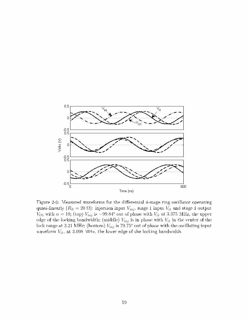
Figure 2-6: Measured waveforms for the differential 4-stage ring oscillator operatingquasi-linearly (𝑅𝐸 = 20 Ω): injection input 𝑉𝑖𝑛𝑗, stage 1 input 𝑉𝑖1 and stage 1 output𝑉𝑂1 with 𝛼 = 10; (top) 𝑉𝑖𝑛𝑗 is −99.84𝑜 out of phase with 𝑉𝑖1 at 3.375 MHz, the upperedge of the locking bandwidth; (middle) 𝑉𝑖𝑛𝑗 is in phase with 𝑉𝑖1 in the center of thelock range at 3.21MHz; (bottom) 𝑉𝑖𝑛𝑗 is 79.75
𝑜 out of phase with the oscillating inputwaveform 𝑉𝑖1, at 3.098 MHz, the lower edge of the locking bandwidth.
19

2.4 Time-Domain Model For Injection Locking in
Differential Ring Oscillators
The 4-stage differential ring oscillator in Fig. 2-3 with zero degeneration resistors
(𝑅𝐸 = 0) has output waveforms which do not have a single dominant frequency
component. Hence, phasor analysis and the frequency domain injection locking
model [50, 52] do not apply. We now derive the time-domain, delay based model to
study the injection-locking phenomena in such oscillators. First, we derive analytical
expressions for the oscillator time-domain waveforms and the effect of an injection sig-
nal in sections 2.4.1 and 2.4.2. They are used to arrive at a delay based model for the
oscillator and expressions for injection-lock range in section 2.4.3. The time-domain
model predictions are compared to measurements and simulations for an experimen-
tal prototype and to the predictions of the quasi-linear model from section 2.3. Using
the delay based, time-domain model we further predict and experimentally verify the
injection-locking dynamics in section 2.4.4.
2.4.1 Analytical Expressions for the Oscillator Waveforms
The operation of a delay stage can be modeled as shown in Fig. 2-7; the 𝑉 −𝐼 converter
(Q1-Q2) acts as comparator on the differential input (𝑉𝐼,𝑝 − 𝑉𝐼,𝑛); its differential
output current is a step waveform with amplitude 𝐼𝐵𝐼𝐴𝑆 which is driven into the
differential load (2𝑅𝐿//𝐶𝐿/2); the differential output voltage 𝑣𝑑 = 𝑉𝑂,𝑝 − 𝑉𝑂,𝑛 is
the step response of the 𝑅 − 𝐶 circuit and thus an exponential waveform as shown
in Fig. 2-8. Assuming an N stage ring oscillator, the falling section of the output
waveform of a stage for 0 ≤ 𝑡 ≤ 𝑇/2 is given by,
𝑣𝑑(𝑡) = −𝑉𝑎,𝑚𝑎𝑥 + (𝑉𝑎 + 𝑉𝑎,𝑚𝑎𝑥) · 𝑒−𝑡𝜏 (2.4)
where 𝑉𝑎 is the amplitude of the oscillations; 𝑉𝑎,𝑚𝑎𝑥 = 𝐼𝐵𝐼𝐴𝑆𝑅𝐿 is the maximum
possible amplitude; 𝜏 = 𝑅𝐿𝐶𝐿 is the load time constant. The next stage has 𝑣𝑑 as an
input and switches its current when 𝑣𝑑 = 0 so that the delay 𝑡𝑑 through each stage
20
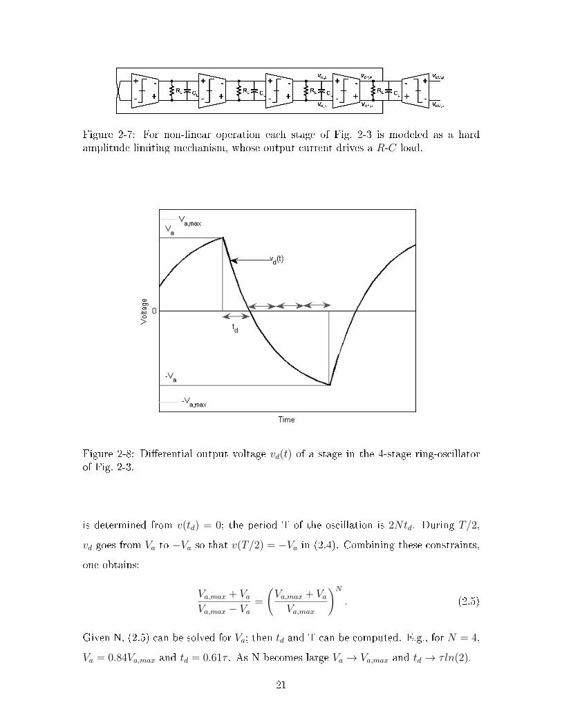
Figure 2-7: For non-linear operation each stage of Fig. 2-3 is modeled as a hardamplitude limiting mechanism, whose output current drives a 𝑅-𝐶 load.
Figure 2-8: Differential output voltage 𝑣𝑑(𝑡) of a stage in the 4-stage ring-oscillatorof Fig. 2-3.
is determined from 𝑣(𝑡𝑑) = 0; the period T of the oscillation is 2𝑁𝑡𝑑. During 𝑇/2,
𝑣𝑑 goes from 𝑉𝑎 to −𝑉𝑎 so that 𝑣(𝑇/2) = −𝑉𝑎 in (2.4). Combining these constraints,
one obtains:
𝑉𝑎,𝑚𝑎𝑥 + 𝑉𝑎
𝑉𝑎,𝑚𝑎𝑥 − 𝑉𝑎
=
(︃𝑉𝑎,𝑚𝑎𝑥 + 𝑉𝑎
𝑉𝑎,𝑚𝑎𝑥
)︃𝑁
. (2.5)
Given N, (2.5) can be solved for 𝑉𝑎; then 𝑡𝑑 and T can be computed. E.g., for 𝑁 = 4,
𝑉𝑎 = 0.84𝑉𝑎,𝑚𝑎𝑥 and 𝑡𝑑 = 0.61𝜏 . As N becomes large 𝑉𝑎 → 𝑉𝑎,𝑚𝑎𝑥 and 𝑡𝑑 → 𝜏 𝑙𝑛(2).
21

Figure 2-9: Effect of the injection signal on the output voltage 𝑣𝑑 = 𝑣𝑑,𝑖 + 𝑣𝑑,𝑖𝑛𝑗
2.4.2 Effect of an Injection Signal
We focus on the first stage’s differential output 𝑣𝑑 = 𝑉𝑂1,𝑝 − 𝑉𝑂1,𝑛 when an injection
signal is present 𝑉𝐼𝑁𝐽,𝑝 − 𝑉𝐼𝑁𝐽,𝑛. Since the output load is linear, the output voltage
𝑣𝑑 can be calculated as the superposition of the output voltage 𝑣𝑑,𝑖 due to the current
𝑖𝑑,𝑖 = 𝐼𝐼1,𝑝−𝐼𝐼1,𝑛 and the output voltage 𝑣𝑑,𝑖𝑛𝑗 due to the current 𝑖𝑑,𝑖𝑛𝑗 = 𝐼𝐼𝑁𝐽,𝑝−𝐼𝐼𝑁𝐽,𝑛
as shown in Fig. 2-9. When the zero crossings of the input voltage of the injection
stage 𝑉𝐼𝑁𝐽,𝑝 − 𝑉𝐼𝑁𝐽,𝑛 have a delay Δ compared to the zero crossings of the input of
the first stage 𝑉𝐼1,𝑝 − 𝑉𝐼1,𝑛, then the transitions in 𝑖𝑑,𝑖𝑛𝑗 have a delay Δ compared to
the transitions in 𝑖𝑑,𝑖. Now, when the output voltage component 𝑣𝑑,𝑖𝑛𝑗 adds to the
component 𝑣𝑑,𝑖, the zero-crossings of 𝑣𝑑 is delayed by an amount 𝑑 compared to the
zero-crossing of 𝑣𝑑,𝑖, which corresponds to the non-injection case. As a result, due
to the presence of the injection signal, the delay through the first stage is increased
by an amount 𝑑 and the oscillator can now oscillate with a period 𝑇 + 2𝑑. We can
develop the relationship between 𝑑 and Δ as follows. The exponentially decreasing
22

part of 𝑣𝑑,𝑖 is given by (2.4) and for 𝑣𝑑,𝑖𝑛𝑗 we obtain:
𝑣𝑑,𝑖𝑛𝑗(𝑡) = −𝑉𝑎𝑖𝑛𝑗,𝑚𝑎𝑥 + (𝑉𝑎𝑖𝑛𝑗 + 𝑉𝑎𝑖𝑛𝑗,𝑚𝑎𝑥) · 𝑒−𝑡+Δ
𝜏 . (2.6)
and we define
1
𝛼=
𝑖𝑑,𝑖𝑛𝑗𝑖𝑑,𝑖
=𝑉𝑎𝑖𝑛𝑗
𝑉𝑎
=𝑉𝑎𝑖𝑛𝑗,𝑚𝑎𝑥
𝑉𝑎,𝑚𝑎𝑥
. (2.7)
The extra delay 𝑑 due to the injection is,
𝑑 = 𝑡𝑧𝑐(Δ)− 𝑡𝑧𝑐(Δ = 0). (2.8)
where 𝑡𝑧𝑐 denotes the time of the zero-crossing of the falling part of the waveform
𝑣𝑑(𝑡). Using (2.8),(2.4) and (2.6), the following relationship is obtained:
𝑑(Δ) = 𝜏 ln
⎛⎝𝑉𝑎,𝑚𝑎𝑥 + 𝑉𝑎 + (𝑉𝑎𝑖𝑛𝑗,𝑚𝑎𝑥 + 𝑉𝑎𝑖𝑛𝑗) · 𝑒Δ𝜏
𝑉𝑎,𝑚𝑎𝑥 + 𝑉𝑎 + 𝑉𝑎𝑖𝑛𝑗,𝑚𝑎𝑥 + 𝑉𝑎𝑖𝑛𝑗
⎞⎠. (2.9)
2.4.3 Injection Locking Range
Fig. 2-10 shows the differential output for each stage in Fig. 2-3 during injection once
lock has been achieved. As the delay Δ is increased, the zero-crossing of 𝑣𝑑 moves
forward, and 𝑑 keeps increasing, until Δ = Δ𝑚𝑎𝑥 with 𝑣𝑑,𝑖(Δ𝑚𝑎𝑥) = −𝑉𝑎𝑖𝑛𝑗; if the
injection waveform is delayed beyond Δ𝑚𝑎𝑥, different waveform segments overlap and
(2.9) is not valid anymore. Additionally, 𝑑 starts decreasing as shown in Fig. 2-13
and we have reached the edge of the lock range. Then (2.4) gives,
𝑒Δ𝑚𝑎𝑥
𝜏 =
(︃𝑉𝑎,𝑚𝑎𝑥 + 𝑉𝑎
𝑉𝑎,𝑚𝑎𝑥 − 𝑉𝑎𝑖𝑛𝑗
)︃. (2.10)
combining (2.10) with (2.7) and (2.9) one obtains:
𝑑𝑚𝑎𝑥 = 𝑑(Δ𝑚𝑎𝑥) = 𝜏 ln
(︃𝑉𝑎,𝑚𝑎𝑥
𝑉𝑎,𝑚𝑎𝑥 − 𝑉𝑎𝑖𝑛𝑗
)︃. (2.11)
23

Figure 2-10: Waveforms for the differential 4-stage ring oscillator when injectionlocked; the last 3 stages have a delay 𝑡𝑑 and the first stage has a delay 𝑡𝑑 + 𝑑 due tothe injection.
Similarly, for negative Δ, the zero-crossing of 𝑣𝑑 keeps moving backward, and 𝑑 keeps
decreasing, until 𝑣𝑑,𝑖(𝑇/2+Δ𝑚𝑖𝑛) = 𝑉𝑎𝑖𝑛𝑗. If Δ is decreased below Δ𝑚𝑖𝑛, the assump-
tions behind the derivation of (2.9) are not valid anymore and 𝑑 starts increasing
again as shown in Fig. 2-13. The minimum 𝑑 is then
𝑑𝑚𝑖𝑛 = 𝑑(Δ𝑚𝑖𝑛) = 𝜏 ln
(︃𝑉𝑎,𝑚𝑎𝑥
𝑉𝑎,𝑚𝑎𝑥 + 𝑉𝑎𝑖𝑛𝑗
)︃. (2.12)
Note that the maximum and minimum delays can be increased and decreased respec-
tively by decreasing 𝛼 and thus increasing the injection current 𝑖𝑑,𝑖𝑛𝑗 and 𝑉𝑎𝑖𝑛𝑗.
We conclude that the presence of the injection signal introduces an extra delay, 𝑑,
in the oscillator’s loop. For a injection signal with period 𝑇𝑖𝑛𝑗 locking can occur if a 𝑑
exists so that 𝑑 = (𝑇𝑖𝑛𝑗−𝑇 )/2. Given that for a given injection level, 𝑑𝑚𝑖𝑛 ≤ 𝑑 ≤ 𝑑𝑚𝑎𝑥,
the following locking bandwidth exits:
𝑇 + 2𝑑𝑚𝑖𝑛 < 𝑇𝑖𝑛𝑗 < 𝑇 + 2𝑑𝑚𝑎𝑥. (2.13)
24

Figure 2-11: Measured waveforms for the differential 4-stage ring oscillator operatingnon linearly (𝑅𝐸 = 0 Ω) with 𝛼 = 10: the injected signal, 𝑉𝑖𝑛𝑗, the stage 1 inputvoltage, 𝑉𝐼1, and the stage 1 output voltage, 𝑉𝑂1, are shown for varying Δ, the delaybetween 𝑉𝐼𝑁𝐽 and 𝑉𝐼1; (top) Δ = Δ𝑚𝑖𝑛 at the upper edge of lock range at 3.61 MHz;𝑡𝑑1, the delay through stage 1, i.e. the delay between 𝑉𝑂1 and 𝑉𝐼1, is 31.4 ns; Δ = 0and 𝑡𝑑1 = 36.1 ns in the middle of the lock range at 3.49 MHz; (bottom) Δ = Δ𝑚𝑎𝑥
and 𝑡𝑑1 = 39.1 ns at the lower edge of the lock range at 3.37 MHz.
Experimental Verification
The same oscillator prototype used for the simulations and measurements in quasi-
linear operation was used to do simulations and take measurements for non-linear
operation. To verify the time-domain model, we operated the oscillator non-linearly
by setting 𝑅𝐸 to 0; the resistors in the injection stage were again adjusted according to
the desired ratio 𝛼. The free running frequency (𝑓𝑜) was measured to be 3.501 MHz.
Measured waveforms at the edges and in the center of the locking bandwidth are
shown in Fig. 2-11.
Measurements, simulations and predictions [using (2.13)] of the edges of the lock-
ing range are plotted in Fig. 2-12 as a function of the ratio 𝛼. In Table 2.1, the mea-
surements for the locking range are compared to predictions using the time-domain
25
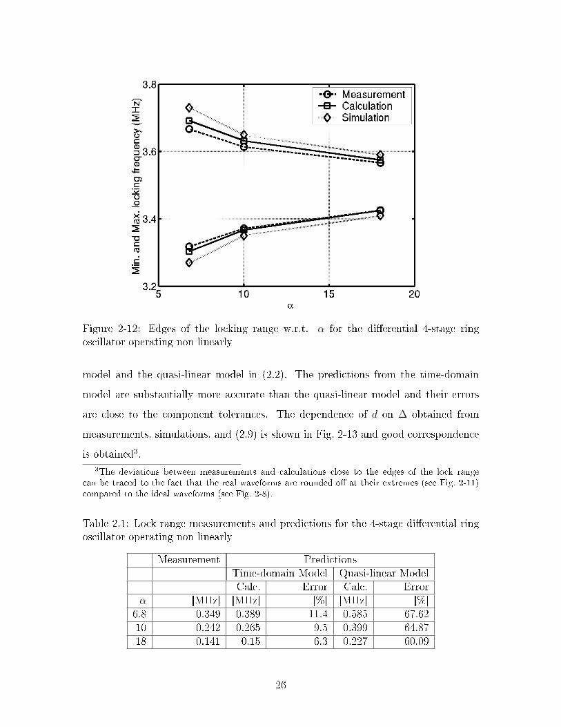
Figure 2-12: Edges of the locking range w.r.t. 𝛼 for the differential 4-stage ringoscillator operating non linearly
model and the quasi-linear model in (2.2). The predictions from the time-domain
model are substantially more accurate than the quasi-linear model and their errors
are close to the component tolerances. The dependence of 𝑑 on Δ obtained from
measurements, simulations, and (2.9) is shown in Fig. 2-13 and good correspondence
is obtained3.
3The deviations between measurements and calculations close to the edges of the lock rangecan be traced to the fact that the real waveforms are rounded off at their extremes (see Fig. 2-11)compared to the ideal waveforms (see Fig. 2-8).
Table 2.1: Lock range measurements and predictions for the 4-stage differential ringoscillator operating non linearly
Measurement PredictionsTime-domain Model Quasi-linear ModelCalc. Error Calc. Error
𝛼 [MHz] [MHz] [%] [MHz] [%]6.8 0.349 0.389 11.4 0.585 67.6210 0.242 0.265 9.5 0.399 64.8718 0.141 0.15 6.3 0.227 60.09
26
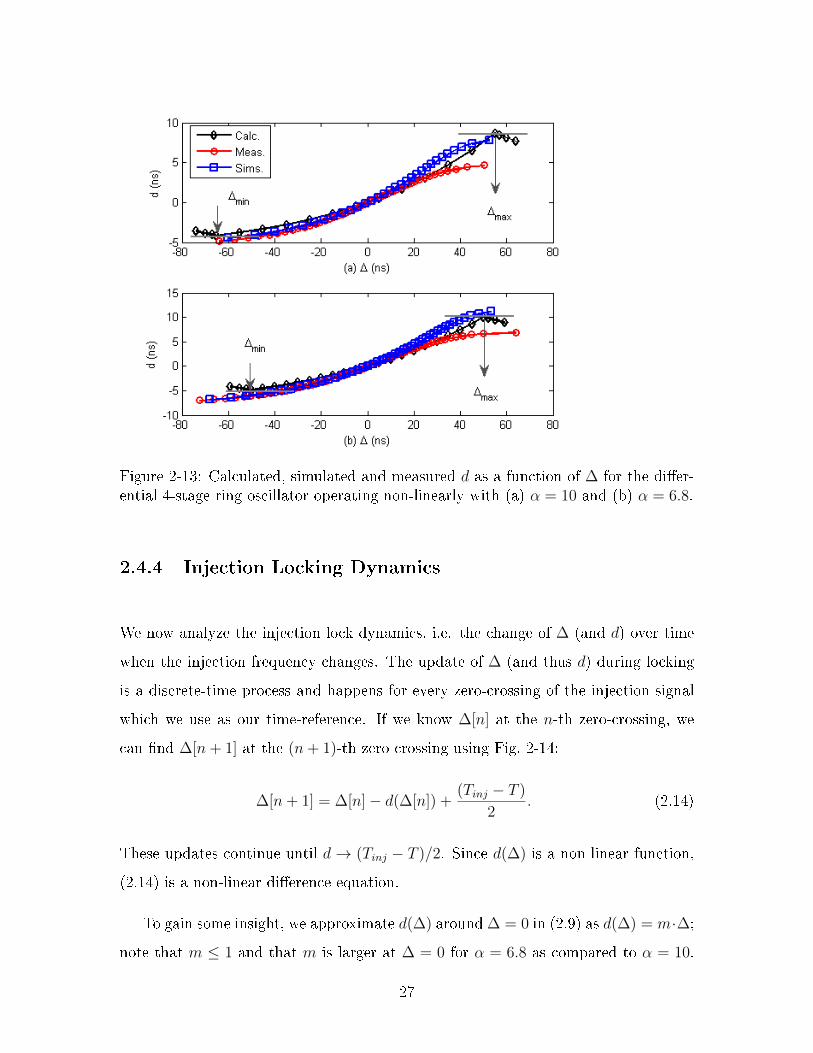
Figure 2-13: Calculated, simulated and measured 𝑑 as a function of Δ for the differ-ential 4-stage ring oscillator operating non-linearly with (a) 𝛼 = 10 and (b) 𝛼 = 6.8.
2.4.4 Injection Locking Dynamics
We now analyze the injection lock dynamics, i.e. the change of Δ (and 𝑑) over time
when the injection frequency changes. The update of Δ (and thus 𝑑) during locking
is a discrete-time process and happens for every zero-crossing of the injection signal
which we use as our time-reference. If we know Δ[𝑛] at the 𝑛-th zero-crossing, we
can find Δ[𝑛+ 1] at the (𝑛+ 1)-th zero crossing using Fig. 2-14:
Δ[𝑛+ 1] = Δ[𝑛]− 𝑑(Δ[𝑛]) +(𝑇𝑖𝑛𝑗 − 𝑇 )
2. (2.14)
These updates continue until 𝑑 → (𝑇𝑖𝑛𝑗 − 𝑇 )/2. Since 𝑑(Δ) is a non-linear function,
(2.14) is a non-linear difference equation.
To gain some insight, we approximate 𝑑(Δ) aroundΔ = 0 in (2.9) as 𝑑(Δ) = 𝑚·Δ;
note that 𝑚 ≤ 1 and that 𝑚 is larger at Δ = 0 for 𝛼 = 6.8 as compared to 𝛼 = 10.
27

Figure 2-14: Injection lock transient waveforms for the differential 4-stage ring oscil-lator used for the derivation of Δ[𝑛+ 1] from Δ[𝑛].
Substituting this linear approximation for 𝑑(Δ) into (2.14), we obtain:
Δ[𝑛] = (1−𝑚)𝑛(Δ[0]− 𝑇𝑖𝑛𝑗 − 𝑇
2𝑚) +
𝑇𝑖𝑛𝑗 − 𝑇
2𝑚. (2.15)
The locking dynamics are then of first order and for larger injection levels (i.e smaller
𝛼 and larger 𝑚) the transient time of a step response is shorter.
Experimental Verification
Fig. 2-15 compares the simulated and calculated evolution of Δ in response to the
injection frequency step change for the prototype oscillator. The simulations and
calculations agree very well.
To experimentally observe the injection lock dynamics, a square wave with the
appropriate amplitude was fed into the FM modulation input of the generator to
obtain the desired step change in the injection frequency and was used to trigger the
real-time oscilloscope to capture the waveforms on the board, as shown in Fig. 2-
28

Figure 2-15: Simulated and calculated injection lock dynamics of the differential 4-stage ring oscillator for a step change in frequency from 3.4MHz to 3.6MHz at 𝛼 = 10(top) 𝛼 = 6.8 (bottom).
16. However, the step change in the injection frequency was not instantaneous after
the step trigger and the injection frequency took few cycles to settle to the new
frequency as can be seen in Fig. 2-17. In order to compare the measured and calculated
dynamics, we wait for 1.5 cycles, take the initial value of Δ at the point shown as
𝑇 = 0 in Fig. 2-17 and then use (2.14) to calculate the dynamics. The measured and
calculated dynamics are plotted in Fig. 2-18 for 𝛼 = 6.8 and 𝛼 = 10 and a very good
correspondence between measurements and model calculations is obtained. Close to
first-order dynamics are observed and, as expected, larger injection levels (smaller 𝛼)
lead to faster settling.
29

Figure 2-16: Experimental setup used to observe the injection lock dynamics of the4-stage differential ring oscillator.
Figure 2-17: After an FM modulation step trigger, the injection frequency generatorsettled to the new frequency in about 1.5 cycles; that time point is labeled as 𝑇 = 0.
30

Figure 2-18: Measured and calculated injection lock dynamics of the 4-stage differen-tial ring oscillators for a step change in frequency from 3.4MHz to 3.6MHz at 𝛼 = 10(top) 𝛼 = 6.8 (bottom).
2.5 Time-Domain Model For Injection Locking in
Single-Ended Inverter Based Ring Oscillator
The delay based method can be used for other types of non-harmonic oscillators as
long as a relationship between the extra stage delay (𝑑) and the delay (Δ) between
the injection signal and the relevant internal oscillator signal is available. This 𝑑-Δ
relationship needs to be developed specifically for the oscillator topology under study
using analytical equations, computer simulations or experimental measurements. In
section 2.4 we derived the d vs. Δ relationship analytically for the differential ring
oscillator in Fig. 2-3.
We now demonstrate the versatility of the delay based method demonstrated by
applying it to a different non-harmonic oscillator, in particular, a single ended inverter
based ring oscillator shown in Fig. 2-19. The the 𝑑 vs. Δ relationship will be derived
using simulations and the appropriate (𝑑𝑚𝑖𝑛,𝑑𝑚𝑎𝑥) will be determined to predicting
31
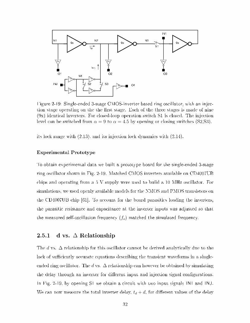
Figure 2-19: Single-ended 3-stage CMOS-inverter based ring oscillator, with an injec-tion stage operating on the the first stage. Each of the three stages is made of nine(9x) identical inverters. For closed-loop operation switch S1 is closed. The injectionlevel can be switched from 𝛼 = 9 to 𝛼 = 4.5 by opening or closing switches (S2,S3).
its lock range with (2.13), and its injection lock dynamics with (2.14).
Experimental Prototype
To obtain experimental data we built a prototype board for the single-ended 3-stage
ring oscillator shown in Fig. 2-19. Matched CMOS inverters available on CD4007UB
chips and operating from a 5 V supply were used to build a 10 MHz oscillator. For
simulations, we used openly available models for the NMOS and PMOS transistors on
the CD4007UB chip [61]. To account for the board parasitics loading the inverters,
the parasitic resistance and capacitance at the inverter inputs was adjusted so that
the measured self-oscillation frequency (𝑓𝑜) matched the simulated frequency.
2.5.1 d vs. Δ Relationship
The 𝑑 vs. Δ relationship for this oscillator cannot be derived analytically due to the
lack of sufficiently accurate equations describing the transient waveforms in a single-
ended ring oscillator. The 𝑑 vs. Δ relationship can however be obtained by simulating
the delay through an inverter for different input and injection signal configurations.
In Fig. 2-19, by opening S1 we obtain a circuit with two input signals IN1 and INJ.
We can now measure the total inverter delay, 𝑡𝑑 + 𝑑, for different values of the delay
32

Figure 2-20: Waveforms and the definition of d and Δ for the single-ended 3-stagering oscillator in Fig. 2-19.
Δ between the inverter input and the injection signal, as shown in Fig. 2-20, and then
obtain the 𝑑 vs Δ relationship shown in Fig. 2-21. For the presented prototype, when
switches S2 and S3 are open, the injection ratio 𝛼 is 9, and when they are closed, the
injection ratio 𝛼 is 4.5.
We also measured the 𝑑 vs. Δ relationship when the oscillator is operating in
closed loop and injection locked. These graphs have been added to Fig. 2-21. Note the
excellent correspondence between the results for both cases. This validates using the
open-loop relationship to predict the injection locking characteristics of ring oscillators
using the basic inverter stages.
We further verified the correspondence between the simulated 𝑑 vs. Δ character-
istic and the characteristic measured on the experimental prototype; excellent corre-
lation is obtained both for 𝛼 = 9 in Fig. 2-22 and for 𝛼 = 4.5 in Fig. 2-23. Also for
closed-loop operation a very good correspondence between measurements and sim-
ulations is obtained for the 𝑑 vs. Δ relationship as shown in Fig. 2-24. We can
now proceed with the calculations of the injection-locking range and injection-locking
33
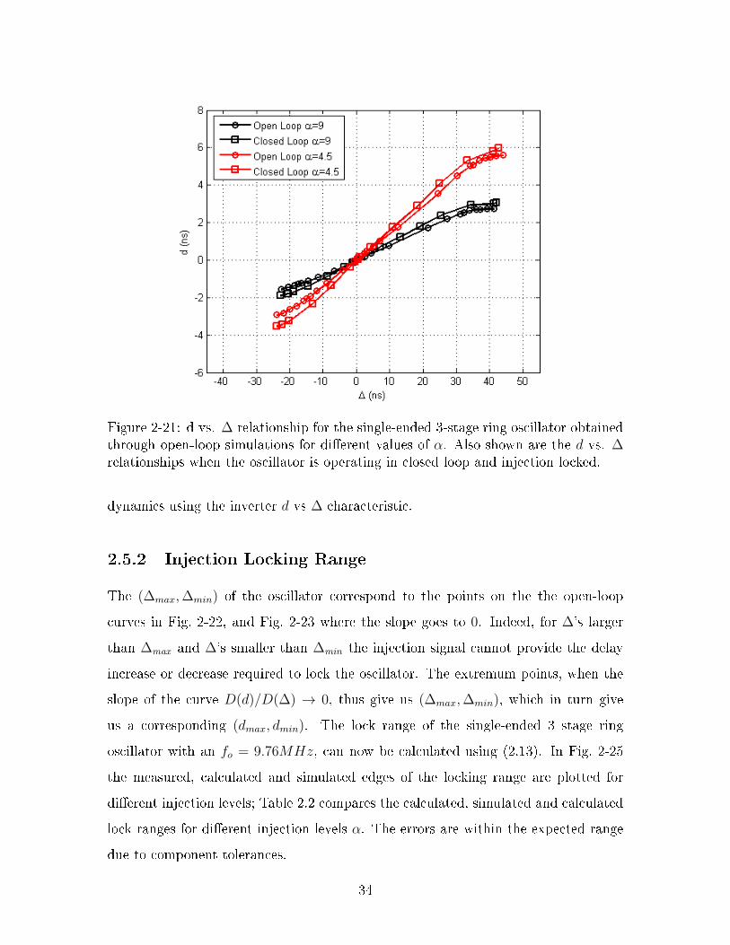
Figure 2-21: d vs. Δ relationship for the single-ended 3-stage ring oscillator obtainedthrough open-loop simulations for different values of 𝛼. Also shown are the 𝑑 vs. Δrelationships when the oscillator is operating in closed loop and injection locked.
dynamics using the inverter 𝑑 vs Δ characteristic.
2.5.2 Injection Locking Range
The (Δ𝑚𝑎𝑥,Δ𝑚𝑖𝑛) of the oscillator correspond to the points on the the open-loop
curves in Fig. 2-22, and Fig. 2-23 where the slope goes to 0. Indeed, for Δ’s larger
than Δmax and Δ’s smaller than Δmin the injection signal cannot provide the delay
increase or decrease required to lock the oscillator. The extremum points, when the
slope of the curve 𝐷(𝑑)/𝐷(Δ) → 0, thus give us (Δ𝑚𝑎𝑥,Δ𝑚𝑖𝑛), which in turn give
us a corresponding (𝑑𝑚𝑎𝑥, 𝑑𝑚𝑖𝑛). The lock range of the single-ended 3 stage ring
oscillator with an 𝑓𝑜 = 9.76𝑀𝐻𝑧, can now be calculated using (2.13). In Fig. 2-25
the measured, calculated and simulated edges of the locking range are plotted for
different injection levels; Table 2.2 compares the calculated, simulated and calculated
lock ranges for different injection levels 𝛼. The errors are within the expected range
due to component tolerances.
34

Figure 2-22: Open-loop d vs. Δ plots obtained through measurements and simulationsat 𝛼 = 9 for the single-ended 3-stage ring oscillator.
Figure 2-23: Open-loop d vs. Δ plots obtained through measurements and simulationsat 𝛼 = 4.5 for the single-ended 3-stage ring oscillator.
35

Figure 2-24: Closed-loop d vs. Δ plots obtained through measurements and simula-tions for the single-ended 3-stage ring oscillator.
Figure 2-25: Edges of the locking range w.r.t. 𝛼 for the single-ended 3-stage ringoscillator
36

Table 2.2: Lock range predictions, measurements, and simulations for the single-ended3-stage ring oscillator
𝑓𝑚𝑖𝑛 𝑓𝑚𝑎𝑥 Lock RangeRel. errorw.r.t. Meas.
[MHz] [MHz] [MHz] [%]𝛼 = 9 Sims 9.18 10.10 0.92 -8𝛼 = 9 Meas 9.10 10.10 1.00 –𝛼 = 9 Calc. 9.26 10.04 0.78 -22
𝛼 = 4.5 Sims 8.80 10.56 1.75 -9𝛼 = 4.5 Meas 8.57 10.42 1.85 –𝛼 = 4.5 Calc. 8.80 10.34 1.54 -31
2.5.3 Injection Locking Dynamics
Using the 𝑑 vs. Δ characteristic and (2.14), we can now also predict the injection
lock dynamics of the oscillator. The simulated and calculated dynamics are shown in
Fig. 2-27 and the measured and calculated dynamics are plotted in Fig. 2-26. A very
good correspondence between measurements, simulations and model calculations is
obtained. Close to first-order dynamics are indeed observed and, as expected, larger
injection levels (smaller 𝛼) lead to faster settling. Note that difference in the final
value of Δ between the measurements and calculations is of the similar size as the
difference between the d vs. Δ relationship obtained under open-loop conditions and
closed-loop conditions in Fig. 2-24.
37

Figure 2-26: Measured and calculated injection lock dynamics for the single-ended3-stage ring oscillator for a step change in frequency from 9.35MHz to 9.75MHz at(top) 𝛼 = 9 (bottom) 𝛼 = 4.5.
Figure 2-27: Simulated and calculated injection lock dynamics for the single-ended3-stage ring oscillator for a step change in frequency from 9.35MHz to 9.75MHz at(top) 𝛼 = 9 (bottom) 𝛼 = 4.5.
38

2.6 Summary
A time-domain delay based model is developed to predict the injection locking be-
havior of non-harmonic oscillators such as ring oscillators. The effect of the injection
signal on the oscillator is modeled with the 𝑑 vs. Δ characteristic which captures
the additional delay, 𝑑, in a stage due the effect of the injection signal with a delay
Δ. Using this characteristic the injection locking range as well as injection locking
dynamics can be accurately modeled and predicted.
This modeling approach is applied to a differential 4-stage ring oscillator where
analytical expressions for the waveforms could be derived along with an analytical
expression for the 𝑑 vs. Δ characteristic. Good correlation is shown between the
predictions, simulations and measurements of the lock range and dynamics at different
injection levels for a prototype oscillator.
Versatility of the modeling approach is demonstrated by analyzing the locking
behavior of a single-ended 3-stage CMOS-inverter based ring oscillator. In this case
accurate analytical expressions for the oscillator waveforms cannot be obtained and
the 𝑑 vs. Δ characteristic is derived from simulations and measurements on a single
inverter stage in open loop. Using this characteristic good correspondence between
predictions for the locking bandwidth and dynamics and measurements and simula-
tions for a prototype oscillator is obtained at different injection levels.
In summary, the presented time-domain delay based modeling approach can be
applied to any non-harmonic oscillator as long as the relationship between the extra
delay, d, and the delay, Δ, between the injection signal and the relevant internal
oscillator is available. As we have shown with examples in this chapter, this relation-
ship can be obtained either analytically or through experimental measurements and
computer simulations.
39

Chapter 3
A 9GHz Sub-Integer Clock-Frequency
Synthesizer at Ultra-Low Supply
3.1 Introduction
Exascale computing capable of atleast a million-trillion operations per second will
be critical for a wide spectrum of applications in science and technology. To reach
such a 100-fold increase in speed over the fastest supercomputers in broad use today
would require extreme parallelism. With such massive parallelism on multiple vertical
levels, the energy required to communicate over billions of parallel threads will be the
critical limitation to energy efficiency [62]. High speed serial communication operating
at ultra-low supplies improves the energy-efficiency and lowers the power envelop of a
system doing an exaflop of loops. The focus area of this chapter is clock synthesis for
such energy-efficient interconnect applications operating at high speeds and ultra-low
supplies.
At high data rates, embedded sub-rate synthesizers and clocking are frequently
used to reduce power [63]. For use in chip-to-chip serial links they require low phase
noise, fast settling and fractional division ratios [64]. Such embedded clock synthesiz-
ers when operated from ultra-low core supply could benefit from lower dynamic power
due to voltage scaling. The ability to operate from the core supply further avoids the
complexities associated with separate supply domains and DC-DC converters, and
40

PFD CP LPF VCO
2:1MUX
PrescalerILRO/3
ProgrammableSub-IntegerDivider
FrequencyCounter
Off-chip Controller
/D:(96,96.5,97,97.5,98,98.5)
𝐹𝑟𝑒𝑓
𝑉𝑐𝑝
𝐹𝑣𝑐𝑜
𝐹𝑓𝑏𝑐𝑙𝑘
𝑉𝑐𝑖𝑙𝑜
𝑏<𝑖>
𝐹𝑖𝑛
𝐶0
𝐹𝐶
𝐶60
𝐶120
𝐹𝑖𝑛𝑗
Figure 3-1: Block diagram of the ultra-low supply sub-integer clock-frequency syn-thesizer using ILRO based prescaler for divide-by-3 function, followed by a phase-switching based sub-integer programmable divider and an automatic injection-lockcalibration loop for ILRO and VCO.
allows for better integration [65, 66]. Earlier clock synthesizers for ultra-low supply
voltage were either limited in speed due to the slow prescaler performance when us-
ing traditional dividers [66], or were limited by the lock range of the injection-locked
frequency dividers used as prescalers [67,68]. Also, these approaches had to resort to
fractional-N synthesis to achieve fine resolution [69].
In this chapter, a 0.5-V, 9-GHz sub-integer clock-frequency synthesizer is presented
demonstrating design techniques to increase speed of operation at ultra-low supply,
such as multi-phase injection-locked prescaler with automatic injection-lock, and fine
frequency resolution using programmable sub-integer divider. On top of these design
advances, it also takes advantage of low V𝑇 and a reduced junction capacitance in
45nm SOI-CMOS to achieve the highest reported speed in literature at this ultra-low
supply.
41
3.2 Architecture and circuit description
The programmable sub-integer synthesizer uses the top-level architecture shown in
Fig. 3-1. It supports feedback division ratios of 96, 96.5, 97, 97.5, 98, and 98.5 over
an output frequency (F𝑣𝑐𝑜) range of 9GHz±1GHz with a reference frequency (F𝑟𝑒𝑓 )
of 95MHz. Using an injection-locked ring oscillator (ILRO) overcomes the speed
roadblock of traditional prescalers at low supplies. Automatic calibration with a
frequency counter and off-chip software control is used to ensure the ILRO is operat-
ing in injection-locking mode. The multiple phases available from the ILRO output
make it possible to implement a fractional division ratio with a phase-switching pro-
grammable divider [70]. This offers the simplicity of an integer-N synthesizer while
achieving fine frequency resolution without compromising loop bandwidth or settling
times. Wider bandwidth and lower division ratios help in further suppression of VCO
phase noise and less amplification of in-band noise. The programmable divider does
not rely on time-varying modulus control to achieve sub-integer division and does
not create fractional spurs, unlike in fractional-N synthesizers. The synthesizer uses
a differential charge-pump (CP), with a similar design as [71] and a nominal current
value of 1mA. A standard differential 2nd-order loop filter is used with a series R-C
(R=8KΩ, C=80pF) in parallel with a 4pF capacitor. The differential filter output
voltage, V𝑐𝑝, tunes the LC VCO. It uses a cross-coupled inverter for low supply volt-
age operation and has a rail-to-rail output signal. For testing purposes, a 2:1 MUX
has been inserted at the VCO output, which can select between the VCO output
or an off-chip input F𝑖𝑛𝑗, or can be tri-stated. The MUX output connects to the
ILRO-based prescaler through AC coupling.
3.2.1 PFD, CP, and VCO
The phase-frequency detector (PFD) design, Fig. 3-2, uses extra delay in reset path to
ensure minimum pulse width to avoid deadzone induced low loop gain and increased
jitter. To increase noise immunity the entire loop including the charge-pump and the
loop filter uses fully differential design. Fig. 3-3 shows this differential charge-pump
42

dffr
dff
r
𝐹𝑟𝑒𝑓
𝐹𝑓𝑏𝑐𝑙𝑘
𝑖𝑛𝑐
𝑑𝑒𝑐
Figure 3-2: PFD with extra delay in reset path.
−
+
−
+
𝑉𝑛𝑏𝑖𝑎𝑠
𝑖𝑛𝑐 𝑖𝑛𝑐
𝑑𝑒𝑐 𝑑𝑒𝑐
𝑑𝑒𝑐 𝑑𝑒𝑐
𝑖𝑛𝑐 𝑖𝑛𝑐
𝐶2𝑅1
𝐶1
𝑉𝑐𝑝
Common-mode Cntrl
Figure 3-3: Differential charge-pump with unity-gain buffer based architecture alongwith common-mode feedback circuit.
43
where a unity-gain buffer based architecture is used along with common-mode control
to keep voltage-controlled oscillator (VCO) voltage (𝑉𝑐𝑝) at optimal value and reject
common-mode noise. At 0.5V supply, this structure has 𝑉𝑐𝑝 range of <200mV to have
>300mV of voltage headroom for saturation region operation of the two stack MOS
transistors. The voltage-controlled oscillator (VCO) uses a cross-coupled inverter
architecture for low supply operation, as shown in Fig. 3-4. The oscillator swings
rail-to-rail and is designed to cover ±1GHz band. It uses a closely-spaced digitally
tuned coarse varactor bank that centers the VCO close to required frequency, and a
finely controlled varactor using the filtered differential control voltage, 𝑉𝑐𝑝. A high
𝐶𝑚𝑎𝑥/𝐶𝑚𝑖𝑛 ratio over a low voltage tuning range implies high varactor 𝑘𝑣, which is
unfavourable to phase noise performance. Differential tuning provides a simple but
effective solution to avoid the drawbacks of high 𝑘𝑣 effect. All low frequency noise,
such as flicker noise, can be considered to be common-mode noise and differentially
tuned varactors can be used to suppress common-mode noise [72]. The VCO fea-
tures differentially tuned MOS varactors to provide fine tuning while diminishing the
adverse effect of high varactor sensitivity through rejection of common-mode noise.
3.2.2 ILRO based Prescaler
Simulations over process, voltage and temperature (PVT) for a nominal 0.5V supply
show that the input frequency of the ILRO-based divider is up to 2X larger than that
of the traditional flip-flop based divider using current-mode-logic latches of [73], while
also operating with lower power and having a smaller area footprint. The traditional
divider has also more demanding signal power requirements on the input clock to fully
steer the currents. The need for voltage headroom of 2V𝐷𝑆𝑆𝐴𝑇 plus the necessary
output amplitude creates a performance ceiling at ultra-low supplies. For example,
V𝐷𝑆𝑆𝐴𝑇 of ∼150mV and output amplitude of ∼300mVpp leads to a minimum supply
requirement of 0.6V. The general multi-phase, multiple-input injection scheme in
Fig. 3-5 increases the locking range of the ILRO based divider and allows to implement
an odd-M division modulus, where M is the odd number of ring-oscillator stages.
Using the Δ → 𝑑 relation, described in [74], such a multiple-input injection widens
44

𝑉𝑑𝑑
𝑉𝑐𝑝
𝑏<𝑖>coarse
Figure 3-4: VCO, using a cross-coupled inverter architecture.
45

.
𝑆1.
𝑆2. ...
Odd-M stage.𝑆𝑀
. . . ... .𝑆𝑖𝑛𝑗
𝑆𝑀
𝑆1
𝑆2
𝑆𝑖𝑛𝑗
Δ
𝑡𝑑 + 𝑑
Δ
ΔΔ Δ
𝑡𝑑 + 𝑑
𝑡𝑑 + 𝑑 𝑡𝑑 + 𝑑
Free-running
osc. delay
in each
stage is
𝑡𝑑, hence
period T
is 2𝑀.𝑡𝑑
In
steady-state
injection-lock,
delay 𝑡𝑑modulated
by d,
a function
of injection
skew Δat multiple
inputs
Injection
period
𝑇𝑖𝑛𝑗 = 2(𝑡𝑑 + 𝑑),leading to
osc. period
of 𝑀.𝑇𝑖𝑛𝑗,
a modulo-M
division
Figure 3-5: General concept of odd-M stage multi-input injection to achieve modulo-M division and achieve wider injection lock range.
46

𝐺𝑥1
𝑣𝑐𝐺𝑥2
𝑣𝑐𝐺𝑥3
𝑣𝑐
𝐺𝑦1𝑣𝑐
𝐺𝑦2𝑣𝑐
𝐺𝑦3𝑣𝑐
𝐶0 𝐶240 𝐶120
𝐶180 𝐶60 𝐶300
𝑉𝑐𝑖𝑙𝑜
𝐹𝑖𝑛
𝐹𝑖𝑛
𝑖𝑛
𝑜𝑢𝑡
𝑣𝑐𝑣𝑏
local
𝐺*
Figure 3-6: Ultra-low voltage pseudo-differential implementation of the ILROprescaler in a divide-by-3 configuration.
the lock range to (𝑇 − 2𝑀.𝑑𝑚𝑖𝑛 < 𝑀.𝑇𝑖𝑛𝑗 < 𝑇 + 2𝑀.𝑑𝑚𝑎𝑥), where T is the period
of the free-running ring-oscillator, T𝑖𝑛𝑗 is the period of the injected signal S𝑖𝑛𝑗 and
(d𝑚𝑖𝑛,d𝑚𝑎𝑥) is the range of delay modulation in each of the oscillator stages due to
steady-state multi-input injection action. In [75] a similar concept was used to obtain
modulo-3 and 7 division ratios at a 1.8V supply. In this work, a generalized time-
domain delay-based approach is used to describe a widening of the lock range with
multi-input injection and is leveraged to implement a modulo-3 ILRO (Fig. 3-6) for
supplies as low as 0.5V. Each stage, G*, of the 3-stage oscillator is inverting with
the transconductance of a NFET driving an active PFET load. The free-running
frequency of the oscillator is set by controlling the load impedance using the bias
voltage V𝑐𝑖𝑙𝑜. The injection signal superimposes on the V𝑐𝑖𝑙𝑜 voltage to modulate the
active load impedance to achieve injection-lock. The differential signal, F𝑖𝑛, from the
2:1 MUX is used to injection lock two coupled 3-stage ring oscillators that generate
the complementary phase-shifted outputs C0/C180, C60/C240, and C120/C300. The
coupling inverters between the complementary phases correct for any phase deviations
and maintain symmetry across this pseudo-differential circuit for an even output phase
47
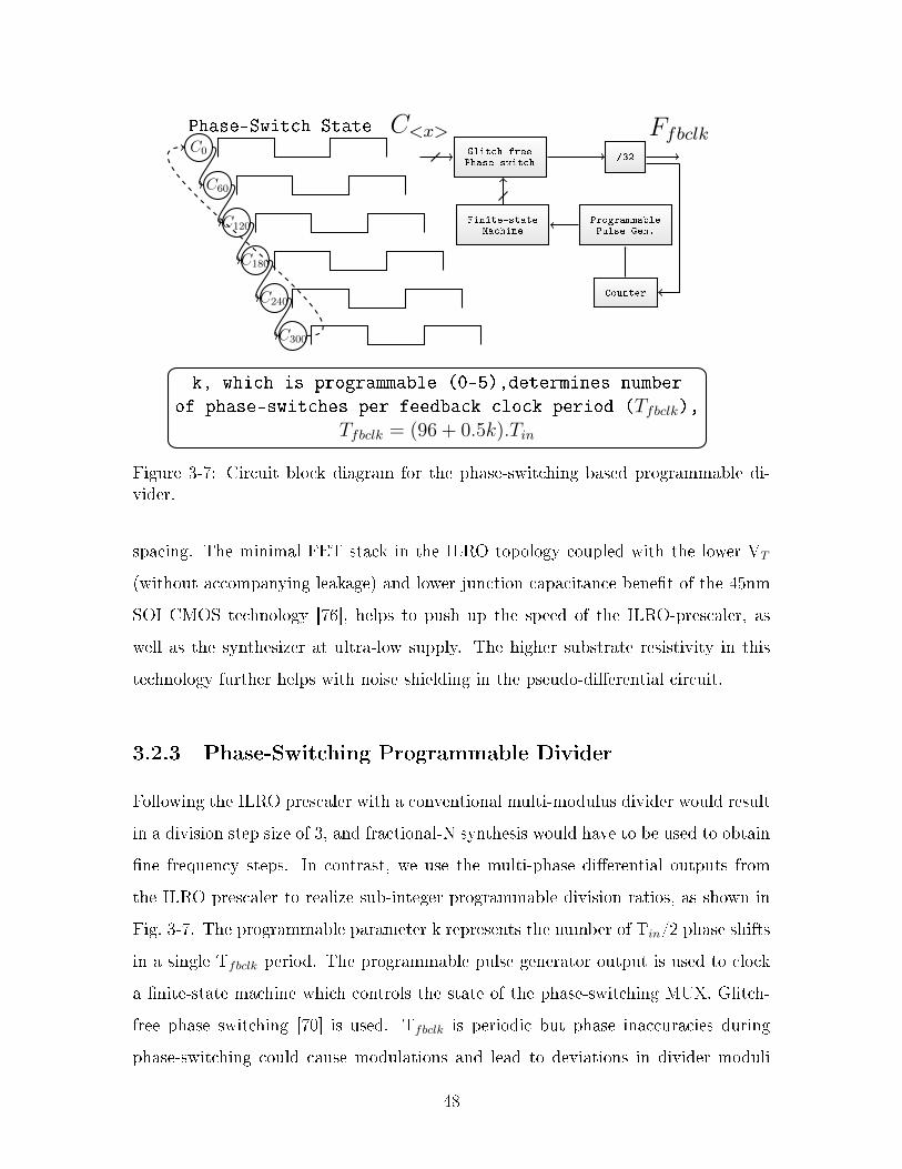
𝐶0
𝐶60
𝐶120
𝐶180
𝐶240
𝐶300
k, which is programmable (0-5),determines number
of phase-switches per feedback clock period (𝑇𝑓𝑏𝑐𝑙𝑘),
𝑇𝑓𝑏𝑐𝑙𝑘 = (96 + 0.5𝑘).𝑇𝑖𝑛
Glitch-freePhase-switch
/32
ProgrammablePulse Gen.
Counter
Finite-stateMachine
𝐶<𝑥> 𝐹𝑓𝑏𝑐𝑙𝑘Phase-Switch State
Figure 3-7: Circuit block diagram for the phase-switching based programmable di-vider.
spacing. The minimal FET stack in the ILRO topology coupled with the lower V𝑇
(without accompanying leakage) and lower junction capacitance benefit of the 45nm
SOI CMOS technology [76], helps to push up the speed of the ILRO-prescaler, as
well as the synthesizer at ultra-low supply. The higher substrate resistivity in this
technology further helps with noise shielding in the pseudo-differential circuit.
3.2.3 Phase-Switching Programmable Divider
Following the ILRO prescaler with a conventional multi-modulus divider would result
in a division step size of 3, and fractional-N synthesis would have to be used to obtain
fine frequency steps. In contrast, we use the multi-phase differential outputs from
the ILRO prescaler to realize sub-integer programmable division ratios, as shown in
Fig. 3-7. The programmable parameter k represents the number of T𝑖𝑛/2 phase shifts
in a single T𝑓𝑏𝑐𝑙𝑘 period. The programmable pulse generator output is used to clock
a finite-state machine which controls the state of the phase-switching MUX. Glitch-
free phase switching [70] is used. T𝑓𝑏𝑐𝑙𝑘 is periodic but phase inaccuracies during
phase-switching could cause modulations and lead to deviations in divider moduli
48

and sub-integer spurs. As an example, a 2ps change in T𝑓𝑏𝑐𝑙𝑘 on average would lead
to deviation of about 0.02% in frequency at F𝑣𝑐𝑜.
3.2.4 Automatic Injection-Lock Calibration
PFD CP LPF VCO
2:1MUX
PrescalerILRO/3
ProgrammableSub-IntegerDivider
FrequencyCounter
Off-chip Controller
/D:(96,96.5,97,97.5,98,98.5)
𝐹𝑟𝑒𝑓
𝑉𝑐𝑝
𝐹𝑣𝑐𝑜
𝐹𝑓𝑏𝑐𝑙𝑘
𝑉𝑐𝑖𝑙𝑜
𝑏<𝑖>
𝐶0
𝐹𝐶
𝐶60
𝐶120
𝐹𝑖𝑛𝑗
Start ILRO cal.
in state shown
above
Inc. 𝑉𝑐𝑖𝑙𝑜
Get 𝐹𝐶
Is |FC-512| decreasing ?
Set 𝑉𝑐𝑖𝑙𝑜
Enter VCO band select
Y
N
Figure 3-8: Automatic injection-lock calibration algorithm to coarsely set the ILROfree-running frequency.
Compared to traditional, divider-based prescalers, ILRO-prescalers can process
inputs with higher frequencies while operating from lower-supplies, but they have a
limited lock range. For a PLL with ILRO prescalers to work reliably over PVT, the
ILRO free-running frequency needs to be set to be within lock range and the VCO
band needs to be selected optimally. The ILRO free-running frequency is calibrated
for in [67], but the calibration scheme presented here in Fig. 3-8 and Fig. 3-9 does
49

PFD CP LPF VCO
2:1MUX
PrescalerILRO/3
ProgrammableSub-IntegerDivider
FrequencyCounter
Off-chip Controller
/D:(96,96.5,97,97.5,98,98.5)
𝐹𝑟𝑒𝑓
𝑉𝑐𝑝
𝐹𝑣𝑐𝑜
𝐹𝑓𝑏𝑐𝑙𝑘
𝑉𝑐𝑖𝑙𝑜
𝑏<𝑖>
𝐶0
𝐹𝐶
𝐶60
𝐶120
𝐹𝑖𝑛𝑗
Start VCO band select
in state shown
above
Set 𝑉𝑐𝑝 = 0 and
inc. 𝑏<𝑖>
Get 𝐹𝐶
Save maximal set of
bands with
monotonically
increasing FC.
Is i < 32 ?
Average of above
maximal set
is optimal VCO band
End
Y
N
Figure 3-9: Automatic injection-lock calibration algorithm to optimally select theVCO band.
50
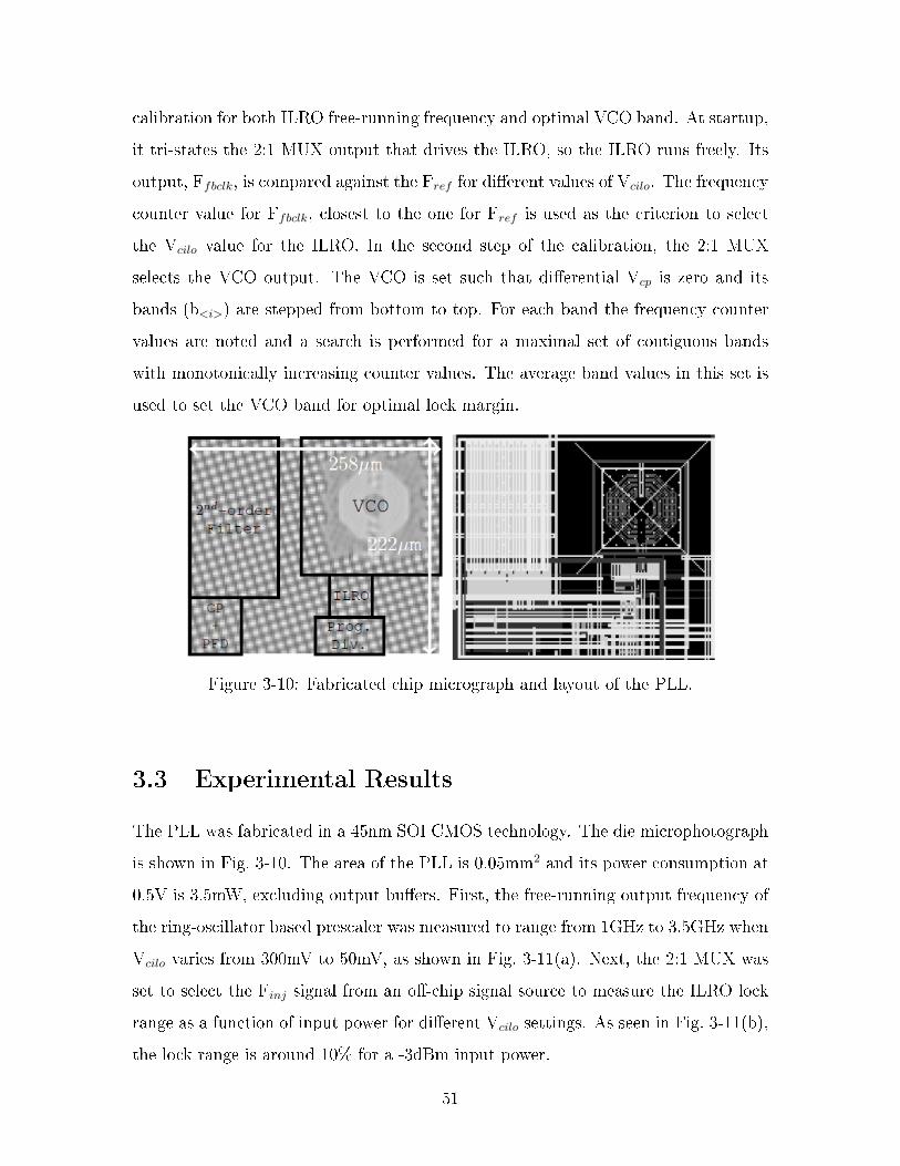
calibration for both ILRO free-running frequency and optimal VCO band. At startup,
it tri-states the 2:1 MUX output that drives the ILRO, so the ILRO runs freely. Its
output, F𝑓𝑏𝑐𝑙𝑘, is compared against the F𝑟𝑒𝑓 for different values of V𝑐𝑖𝑙𝑜. The frequency
counter value for F𝑓𝑏𝑐𝑙𝑘, closest to the one for F𝑟𝑒𝑓 is used as the criterion to select
the V𝑐𝑖𝑙𝑜 value for the ILRO. In the second step of the calibration, the 2:1 MUX
selects the VCO output. The VCO is set such that differential V𝑐𝑝 is zero and its
bands (b<𝑖>) are stepped from bottom to top. For each band the frequency counter
values are noted and a search is performed for a maximal set of contiguous bands
with monotonically increasing counter values. The average band values in this set is
used to set the VCO band for optimal lock margin.
Figure 3-10: Fabricated chip micrograph and layout of the PLL.
3.3 Experimental Results
The PLL was fabricated in a 45nm SOI CMOS technology. The die microphotograph
is shown in Fig. 3-10. The area of the PLL is 0.05mm2 and its power consumption at
0.5V is 3.5mW, excluding output buffers. First, the free-running output frequency of
the ring-oscillator based prescaler was measured to range from 1GHz to 3.5GHz when
V𝑐𝑖𝑙𝑜 varies from 300mV to 50mV, as shown in Fig. 3-11(a). Next, the 2:1 MUX was
set to select the F𝑖𝑛𝑗 signal from an off-chip signal source to measure the ILRO lock
range as a function of input power for different V𝑐𝑖𝑙𝑜 settings. As seen in Fig. 3-11(b),
the lock range is around 10% for a -3dBm input power.
51

0.1 0.2 0.3 0.4
1
2
3
4
·109
𝑉𝑐𝑖𝑙𝑜 (V)
(a)
Frequency
(Hz)
4 5 6 7 8 9
·109
−12
−10
−8
−6
−4
ILRO Injection Freq. (Hz)
(b)
Input
(dBm)
𝑉𝑐𝑖𝑙𝑜 = 0.2𝑉 𝑉𝑐𝑖𝑙𝑜 = 0.15𝑉 𝑉𝑐𝑖𝑙𝑜 = 0.1𝑉
Figure 3-11: Measurement of (a)𝑉𝑐𝑖𝑙𝑜 versus 𝐹𝑜𝑠𝑐 (b) Input dBm versus Freq. lockrange.
52

Process and back-end-of-line (BEOL) interconnect parasitic parameters are ad-
justed in simulation to match the measured self-oscillation frequency of the oscilla-
tor. These parameters are then used to simulate for open-loop d vs. Δ relationship
for the delay stages at different input signal levels. The extremum points in these
curves, where 𝑠𝑙𝑜𝑝𝑒 → 0, gives the corresponding (𝑑𝑚𝑎𝑥, 𝑑𝑚𝑖𝑛) values; the range of
delay modulation in each of the oscillator stages due to injection action. The lock
ranges can be calculated using (𝑇 − 6.𝑑𝑚𝑖𝑛 < 𝑙𝑜𝑐𝑘 − 𝑟𝑎𝑛𝑔𝑒 < 𝑇 + 6.𝑑𝑚𝑎𝑥), where
T is the period of the free-running ring-oscillator. In Fig. 3-12, the linear-fit of the
measured and calculated lock range values are plotted at different input levels and
self-oscillation frequencies, showing a good model-to-hardware correlation.
−12 −11 −10 −9 −8 −7 −6 −5 −4 −3100
200
300
400
500
600
700
800
900
1,000
1,100
Input (dBm)
LockRange(MHz)
d vs. Δ model𝑉𝑐𝑖𝑙𝑜 = 0.2𝑉 , meas.d vs. Δ model
𝑉𝑐𝑖𝑙𝑜 = 0.15𝑉 , meas.d vs. Δ model
𝑉𝑐𝑖𝑙𝑜 = 0.1𝑉 , meas.
Figure 3-12: Linear-fit of measured and calculated lock ranges at different injectioninput levels and self-oscillation frequencies.
Fig. 3-13(a) shows the plot of min-max frequency in each VCO band, as well as the
mid-band frequency with differential V𝑐𝑝 set to 0. The frequency counter values during
53

0 5 10 15 20 25 307
8
9
10
11
12
VCO bands
(a)
Frequency
(GHz)
Fmin𝑉𝑐𝑝 = 0Fmax
0 5 10 15 20 25 30
500
520
540
VCO bands
(b)
Frequency
CountValue
Convergence
to VCO band
18 for
optimal lock
Figure 3-13: (a)Vco gain curves. (b) Auto-calibration between ILRO and VCO.
54

automatic injection-lock calibration are also shown in Fig. 3-13(b), and it converges to
VCO band 18, the average of the maximal set of bands with monotonically increasing
count values, for optimal injection-lock point. The ILRO lock range is large enough to
maintain lock over supply and temperature drift, thus removing the need for dynamic
calibration.
Fig. 3-14(a) shows the PLL output spectrum at different sub-integer division ratios
using F𝑟𝑒𝑓 of 95MHz, a frequency resolution of 47.5MHz is observed in the spectra.
The phase-noise at a single divider setting is shown in Fig. 3-14(b), but at all divide
ratios the phase noise value is close to -100 dBc/Hz at 1MHz offset. While it is difficult
to determine the source of the correlation for the spurs seen in the phase noise plot,
the estimated jitter contribution due to these spurs is less than few fs. Integrated
RMS jitter beyond the clock-data recovery corner frequency (baudrate/1667) is 325fs,
which compares favourably for use in high-speed serial communications [77].
Table 3.1: Performance Summary and Comparison of Low-Supply PLLs.
This Work [66] [67] [68] [78]
CMOS Tech. 45nm-SOI 65nm 65nm 65nm 180nm
𝐹𝑣𝑐𝑜 (GHz) 9.12 2.4 5.49 5.54 1.9
𝐹𝑣𝑐𝑜/𝐹𝑟𝑒𝑓 96 2400 160 160 126
PLL-type Sub-Int-N Int-N Int-N Int-N Int-N
VCO LC LC LC LC LC
Supply (V) 0.5 0.68 0.5 0.5 0.5
Power (mW) 3.5 0.68 0.95 1.6 4.5
Area (𝑚𝑚2) 0.05 0.2 0.78 0.64 1.32
PN (dBc/Hz) -100 -110 -106 -105 -120.4
Ref. Spur (dBc) -61 -50 -65 -65 -44
FOM𝑎 -173.5 -179 -181 -179 -179.4
FOM𝑏𝐴 -186.5 -186 -183 -181 -178.2
𝐹𝑂𝑀𝑎 = 𝑃𝑁 − 20.𝐿𝑜𝑔(𝐹𝑣𝑐𝑜/1𝑀𝐻𝑧) + 10.𝐿𝑜𝑔(𝑃𝑜𝑤𝑒𝑟/1𝑚𝑊 )𝐹𝑂𝑀 𝑏
𝐴 = 𝐹𝑂𝑀 + 10 · 𝐿𝑜𝑔(𝐴𝑟𝑒𝑎/1𝑚𝑚2)
Fig. 3-15, shows the distribution of the power consumption over different macros
55

0.86 0.88 0.9 0.92 0.94 0.96 0.98 1
·1010
−100
−80
−60
−40
−20
Frequency (Hz)
(a)
dBm
𝐹𝑟𝑒𝑓 × 96𝐹𝑟𝑒𝑓 × 96.5𝐹𝑟𝑒𝑓 × 97𝐹𝑟𝑒𝑓 × 97.5𝐹𝑟𝑒𝑓 × 98𝐹𝑟𝑒𝑓 × 98.5
Figure 3-14: Measurement of (a) Output spectra of the clock-frequency synthesizerat different sub-integer division ratios. (b) Phase noise plot at division ratio of 96.
56

VCO15.7%
ILRO-Prescaler28.6%
Prog. Div.44.3%
PFD+CP11.4%
Figure 3-15: Power consumption distribution in the sub-integer clock-frequency syn-thesizer.
in the synthesizer. Table 3.1 summarizes the performance of the synthesizer and com-
pares it against other ultra-low supply PLL implementations. The ultra-low voltage
ILRO-prescaler topology used with automatic injection-lock calibration enabled the
demonstration of a PLL with the highest speed at an ultra-low supply of 0.5V. The
sub-integer programmable divider facilitates fine frequency resolution without requir-
ing a decrease in F𝑟𝑒𝑓 or an increase in the division ratio or a lowering of the loop
bandwidth. The design achieves an outstanding overall FOM𝐴 of -186.5.
3.4 Summary
This chapter presented a sub-integer clock-frequency synthesizer architecture that
can operate at a high speed from an ultra-low supply. A record speed of 9GHz has
been demonstrated at 0.5V in 45nm SOI CMOS. Key design features are described
to achieve such high frequencies with fine resolution at an ultra-low supply. The pro-
posed multi-phase multi-input ILRO-prescaler eliminates the speed bottleneck, while
57
automatic injection-lock calibration ensures lock between the VCO and the ILRO-
prescaler. The phase-switching based programmable divider structure provides fine
frequency resolution through sub-integer division. The PLL power/area are 3.5mW
and 0.05mm2, RMS jitter is 325fs, yielding a FOM𝐴 of -186.5.
58

Chapter 4
A 19Gb/s Receiver for Chip-to-Chip
Links with Clock-Less DFE and
High-BW CDR based on
Master-Slave ILOs
4.1 Introduction
High performance computing (HPC) is an indispensable tool for fundamental un-
derstanding and for prediction of properties of materials and entire systems. HPC
advancement is critical for needs of scientific discovery and economic competitiveness.
Some of the key challenges in advancing to an exascale computing system at 1000x the
performance of today’s petaflop machines include: a thousand-fold increase in par-
allelism, memory storage and data movement requirement, reliability of the system,
and energy consumption at this scale of on-die interconnect [79].
Energy-efficient circuits and architectures for high bandwidth, low latency, and
error-free information transfer over very short-reach (VSR) copper interconnects are
critically needed for chip-to-chip (C2C) communication in high-density, extreme-scale
systems [80]. Source-synchronous links are used in HPC systems for low-power C2C
59

interconnects [81–83]. In such links, because of the existence of the clock lane a fast
CDR is not used leading to uncorrelated jitter, between clock and data as a function
of skew, and resultant performance degradation [84]. Also, in extreme-scale systems
with billions of threads in high-density VSR links, such an synchronous architecture
stresses clock-tree planning, distribution, resilience to failure and increases potential
for electromagnetic interference (EMI). An asynchronous clock architecture with ref-
erence clocks and high BW CDR [85, 86] eases clock tree distribution and enables
the adoption of spread-spectrum clocking (SSC) to suppress EMI. But, in extreme-
scale systems it would still be limited by its power-efficiency and need for reference
clock-tree planning. Reference-less architecture removes the need for clock-tree plan-
ning but usually are limited either by the data rate [87], degree of RX equalization
capability [87], or CDR bandwidth for jitter-tolerance [88,89].
In this chapter a receiver is proposed with an embedded reference-less clocking
architecture that relaxes clock-tree planning in dense systems, while maintaining RX
equalization capability for error-free operation over VSR channels (< 20 − 𝑖𝑛𝑐ℎ dis-
tance). The RX has been implemented in 14nm CMOS and characterized at 19Gb/s.
The receiver features an embedded injection-locked oscillator (ILO) for high BW CDR
to be used with SSC to mitigate EMI and to potentially relax TX jitter specifications
for improved power efficiency. It also has master-slave ILOs based phase genera-
tion/rotation using resistively-interpolated injection edges for optimal placement of
sampling clocks and clock-less DFE for residual first post-cursor equalization. The
next section describes the RX architecture followed by description of different circuit
blocks to explain the unique features. The measurement section presents data on the
quality of the recovered clock and on the RX performance.
60

4.2 System-level Considerations
4.2.1 Channel Equalization
VSR-C2C links typically operate over a range of channel characteristics, ranging
from C2C interconnects within multi-chip modules to relatively short (< 20-inch)
channels across a PCB made up of higher quality material such as Megtron-6. Channel
insertion losses of < 15dB at 10GHz are expected [90] for such VSR links. NRZ
signaling is preferred over PAM4 for such links in extreme-scale systems as they
have no forward-error correction (FEC) protocols to minimize system complexity and
decode latency. To support high IO density and stringent power requirements in
extreme-scale systems, the proposed design envisions a simplified transmitter with no
feed-forward equalizer (FFE) and relaxed amplitude and output jitter specifications.
The design relies solely on the RX for channel equalization. Lack of de-emphasis
on TX (no FFE) increases average signal level at RX input. Continuous-time linear
equalization (CTLE) on the RX side using peaking amplifier can equalize pre- and
post- cursor ISI over wide time span by convolving with impulse response of the
channel. But, counting on RX CTLE leads to one fundamental limitation. It provides
no discrimination between desired signal and noise. Boosting high-frequency signals
relative to low frequency ones not only compensates the loss of the channel but it
amplifies high frequency cross-talk of other channels. A potential concern in high-
density environments of extreme-scale systems. A key advantage of a DFE is that
it is able to compensate for ISI without amplifying noise. RX equalization scheme
shown in Fig. 4-1 has 1-tap DFE and CTLE with 8dB of peaking at half-baud rate,
both can be brought to bear on the channel for optimal performance [91].
Channel operating margins at high data rates are used to measure channel per-
formance that includes both signal impairments and techniques used to compensate
for these impairments [92, 93]. Such a model is used to evaluate the planned RX
CTLE and DFE equalization scheme (Fig. 4-1) to see the impact of the choice and
its effectiveness for a VSR-C2C communication channel. The model includes a trans-
mitter (with no FFE), channel induced frequency dependent attenuation, dispersion
61

and discontinuities as well as voltage noise (from devices), static noise (quantization
errors, RX meta-stability, etc), jitter in timing circuits and clock-data recover loop.
The parameters used are listed in Table 4.1.
Table 4.1: Shows the many parameters used for channel margin study
Parameter Symbol Value
Number of signal Levels L 2
Signaling rate 𝑓𝑏 20Gb/s
Transmitter different peak output 𝐴𝑣 0.6V
Single-ended termination resistor 𝑅𝑑 48Ω
Rx 3dB bandwidth 𝑓𝑟 0.75×𝑓𝑏
Tx FFE 𝐶𝑖 𝑖 = 0
CTLE DC gain 𝑔𝐷𝐶 0-1dB
CTLE peaking at 𝑓𝑏/2 𝑓𝑧,𝑓𝑝1,𝑓𝑝2 0-8dB at 𝑓𝑏/2
DFE length 𝑁𝐷𝐹𝐸 1-UI
RMS RJ 𝜎𝑅𝐽 470fs
Amplitude noise RMS 𝐴𝑚 3mV
Sampler overdrive 𝐴𝑜𝑣 15mV
Sinusoidal jitter sj 200ppm
Target error rate BER 10−12
The analysis, done at 20Gbps over a channel with > 16𝑑𝑏 insertion-loss at 𝐹𝑏𝑎𝑢𝑑/2,
shows adequate margins for horizontal and vertical eye opening at 10−12 BER in
Fig. 4-2. It also shows that by including 1-tap DFE capability the system has the
ability to improve signal-to-noise ratio in the presence of crosstalk by dialing down
the peaking in the CTLE.
62

CTLE
SymbolDecode
+
ℎ1 · 𝑋(𝑧) · 𝑧−1
DFE
ℎ1 used to cancel 1𝑠𝑡-post cursor ISI
Clock Recovery
𝐹𝑏𝑎𝑢𝑑/2
0-8dB 𝑋(𝑧) ·𝐻(𝑧)Output𝑅𝑥𝐼𝑛𝑝𝑢𝑡
Figure 4-1: RX equalization capabilities, such as CTLE peaking and 1-tap DFE areevaluated for channel performance margins.
4.2.2 Receiver Architecture
The block diagram of the quarter-rate RX architecture is shown in Fig. 4-3. This
architecture picked NRZ signaling over PAM4 as latency requirements for this ap-
plication do not support FEC. The architecture further assumes standard encoding
techniques such as 8b10b are used to maintain a minimum transition density for min-
imal overhead. The RX input data path has a peaking amplifier to provide linear
equalization, with a nominal range of 0-8dB at half-baud frequency. The residual 1𝑠𝑡
post-cursor is then removed using a clock-less direct-feedback DFE, before feeding
to two quarter-rate sampling paths (Data/Edge). The samples at the center of the
eye (Data) and at the transition edge (Edge) are de-multiplexed to bang-bang phase-
frequency detectors (BB-PD, BB-FD) for digital phase and frequency control, similar
to [87]. The reference-less BB-FD results in wide capture range and by setting the
frequency control voltage of the ILOs to be in the middle of its dead-zone width it
ensures optimal lock point for the edge-detect injection.
To improve jitter tolerance (JTOL), the NRZ data sequence at the continuous-
time linear-equalizer (CTLE) output is amplified and XORed with its delayed version
63

to detect the transition edges. This edge-detect output resembles RZ data and has
strong clock spectral lines at the data rate 𝐹𝑏𝑎𝑢𝑑 providing a vigorous injection signal
for the master injection-locked oscillator (MILO). The delay between the 2 XOR
inputs is correlated to the frequency-control operation of the BB-FD for the ILO
oscillators and hence maintains a 𝑇𝑏𝑖𝑡/2 spacing for strongest injection. Incidentally,
this same delayed input to XOR for edge-detection is shared to feedback 𝑋(𝑧) · 𝑧−1
symbol for DFE 1𝑠𝑡 post-cursor equalization. Such a clock-less DFE is possible due to
the tight correlation of the delay cell to the MILO-SILO frequency control operation
and the resultant 𝑇𝑏𝑖𝑡/2 spacing.
The MILO then injection locks the slave injection-locked oscillator (SILO); this
improves phase-noise of the SILO and mitigates high frequency jitter transfer to the
SILO’s recovered output clock. The BB-PD ensures optimal timing margin for the
eye center sampler by changing the phases of the SILO recovered clock using coarse
selection of MILO phases and resistively-interpolating the edges finely for injection
into the SILO, leading to linear 360𝑜 phase rotation of the recovered clock. Two
synchronized dividers at SILO output generate quarter-rate clocks for the sampling
latches. Quarter-rate clocking allows more time for critical operations such as sam-
pling latch evaluation thereby avoiding the limitation caused by large over-head of
self-capacitance. Reduced clock tree depth loading in this embedded clock archi-
tecture leads to reduced dynamic clocking power and minimal phase errors in the
quarters, which in turn lessens the need for elaborate clock phase corrections in the
quarters as in [94,95].
64

(a) Horizontal Eye Opening (%)
(b) Vertical Eye Opening (mV)
Figure 4-2: Channel operating margin study with signal impairments at different RXpeaking and DFE settings. 1-tap DFE gives robustness to system solution in case ofdegradation due to crosstalk and PN-skew. To improve signal-to-noise ratio in faceof crosstalk, peaking could be dialed down and ℎ1-tap could be used for post-cursorequalization. 65

𝑅𝑥𝐼𝑛𝑝𝑢𝑡
Supply 𝐼𝑏𝑖𝑎𝑠
Off-chip
Control
Gnd
Vdd
𝑅𝑡𝑒𝑟𝑚
𝑓𝑏𝑎𝑢𝑑/2CTLE
BB-PD
BB-FD
Deserializer
Err. Check
+
DFE
LA
Replica
Buf.
-
Edge
Detect
𝑓𝑏𝑎𝑢𝑑
MILO SILO
Phase
Interpolator
÷2
÷2
𝑓𝑏𝑎𝑢𝑑/2
Serial
scan
Data
Edge
𝐹𝑟𝑒𝑞.𝑐𝑛𝑡𝑟𝑙
𝑓𝑏𝑎𝑢𝑑/4
𝑅𝑒𝑐.𝑐𝑙𝑘
Figure 4-3: Quarter-rate RX architecture for very short-reach chip-to-chip links withclock-less DFE and high-bandwidth CDR based on Master-Slave injection-locked os-cillators.
66

4.3 Circuit Blocks and Descriptions
4.3.1 CTLE
Fig. 4-4, shows the detailed schematic of the CTLE as well as a single-ended repre-
sentation. It controls high-frequency gain peaking, uniquely functions as the current-
summer node for the clock-less direct-DFE, and interfaces to the Data/Edge samplers.
The peaking is adjusted by switching the value of the capacitor 𝐶𝑐 between two par-
allel input stages 𝑔𝑚1𝐴 and 𝑔𝑚1𝐵. The DC gain is 𝑔𝑚1𝐴 · 𝑅1𝐴, while the maximum
possible high frequency gain is (𝑔𝑚1𝐴 + 𝑔𝑚1𝐵) · (𝑅1𝐴//𝑅1𝐵). Without inductor 𝐿1𝐵,
the achievable high frequency gain is limited by the output pole. The inductor 𝐿1𝐵
extends the bandwidth thereby increasing the peaking at 𝐹𝑏𝑎𝑢𝑑/2. The DFE feedback
tap current is summed into the load resistor, 𝑅1𝐴. The clock-less DFE feedback relies
on a replica buffer of the MILO-SILO delay cells to vary the delay according to bau-
drate. It is described in detail latter in the chapter after a discussion on MILO-SILO
frequency calibration.
4.3.2 Data Edge-Detection and Injection
For a random NRZ data stream, each bit in the sequence has an equal probability
(50%) of being a one or a zero, regardless of the state of the preceding bit(s). It
is therefore possible to have large sequences of consecutive identical digits (CIDs).
Because of the very low frequency content produced by long sequences of CIDs in the
data signal, designing high-speed systems that can work with random data can be
difficult. Data encoding, or scrambling, is often used to format the random data into
a more manageable form. This architecture utilizes a widely used encoding method
in high-speed systems, 8b10b, to limit the pattern length and maintain minimum
transition density for minimal overhead. The power spectrum for a NRZ data stream
in Fig. 4-5 shows an infinite sequence of discrete spectral lines (delta functions) scaled
by a "𝑠𝑖𝑛𝑐2(𝑓)" envelope, where 𝑠𝑖𝑛𝑐(𝑓) is defined as 𝑠𝑖𝑛(𝜋𝑓)/(𝜋𝑓). Important ob-
servations that apply to test patterns in general include: (a) the nulls in the 𝑠𝑖𝑛𝑐2(𝑓)
67

𝑔𝑚1𝐵
𝑅1𝐵
𝐿1𝐵
𝑔𝑚1𝐴
𝑅1𝐴
𝑣𝑖
𝑣𝑜
𝐶𝑐
𝐹𝑏𝑎𝑢𝑑/2
0-8dB
𝑔𝑚1𝐴 ·𝑅1𝐴
(𝑔𝑚1𝐴 + 𝑔𝑚1𝐵) · (𝑅1𝐴||𝑅1𝐵)
𝑔𝑚1𝐴
𝑔𝑚1𝐵
. . .
𝑅1𝐵
𝐿1𝐵
𝐶𝑐
. . .𝑅1𝐴
dfe
Freq. resp.
Single-ended
Figure 4-4: RX CTLE equalization using a single-stage peaking amplifier.
68

envelope occur at integer multiples of the data rate; (b) spectral lines are evenly
spaced at an interval that is the inverse of the pattern length; and (c) the magnitude
of the 𝑠𝑖𝑛𝑐2(𝑓) envelope decreases as the data rate and/or pattern length increase.
Figure 4-5: Power spectrum of NRZ signalling for a L-bit repeating pattern, showinga null at data rate.
Since the transitions of the random data sequence is still random the spectrum
of the generated pulses from a NRZ data stream resembles that of a return-to-zero
(RZ) data. RZ data spectrum displays as a square of sinc function with strong clock
spectral lines at data rate and the harmonics. Maintaining 𝑇𝑏/2 delay, where 𝑇𝑏 is
a bit interval, between the two inputs of the XOR gate yields a strong clock spectra
line at data rate, as shown in Fig. 4-6. In fact, the normalized magnitude of 1/𝑇𝑏
line can be expressed as (𝑠𝑖𝑛𝑥𝜋)/𝜋 where 𝑥 (0 < 𝑥 < 1)represents the relative pulse
width [96].
Recovered clock which can track data jitter based on instantaneous locking tech-
niques improve jitter-tolerance and are of use in applications without strict specifica-
tions on jitter transfer. This design extracts the clock at data rate for injection into
the ILO to achieve high jitter-tolerance. The proposed scheme is shown in Fig. 4-7,
where the data edge-detector is used to reproduce the clock for injection. The pulse
generated by the XOR gate not only indicates data transitions but creates strong
spectral line at the data rate (𝐹𝑏𝑎𝑢𝑑), facilitating the injection locking of the subse-
quent MILO-SILO oscillators (to 𝐹𝑏𝑎𝑢𝑑/2).
69
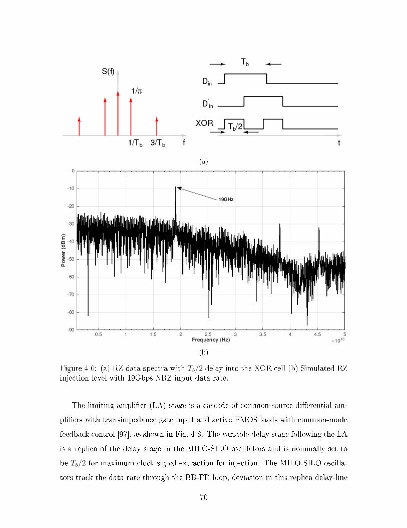
(a)
(b)
Figure 4-6: (a) RZ data spectra with 𝑇𝑏/2 delay into the XOR cell (b) Simulated RZinjection level with 19Gbps NRZ input data rate.
The limiting amplifier (LA) stage is a cascade of common-source differential am-
plifiers with transimpedance gate input and active PMOS loads with common-mode
feedback control [97], as shown in Fig. 4-8. The variable-delay stage following the LA
is a replica of the delay stage in the MILO-SILO oscillators and is nominally set to
be 𝑇𝑏/2 for maximum clock signal extraction for injection. The MILO-SILO oscilla-
tors track the data rate through the BB-FD loop, deviation in this replica delay-line
70

Figure 4-7: Edge-detection, clock signal extraction and injection scheme.
(Fig. 4-9) is simulated to have a 3-𝜎 variation of ±1.5ps due to mismatch. The output
of LA (𝐷𝑖𝑛) and the delay-line (𝐷′𝑖𝑛) are input into the CML XOR stage, Fig. 4-10,
to extract the clock signal for injection into the MILO.
𝑑𝑝 𝑑𝑛
𝑉𝑏𝑛
𝑧𝑛 𝑧𝑝
Common-modeControl
Figure 4-8: Schematics of limiting-amplifier used for ∼20dB differential gain.
4.3.3 Reference-less frequency acquisition
Reference-less here implies a receiver that can function without a physical external
reference clock over a wide incoming data rate. By avoiding reference or forwarded
clocks to the receiver, the clock-tree and frequency planning becomes simpler and
71

𝐷𝑖𝑛 𝐷𝑖𝑛′
𝑉𝑟𝑒𝑔 𝐶𝐿
𝐶𝐿
Replica Delay-Cell
(a)
(b)
Figure 4-9: (a) The replica delay-line uses the regulated-voltage of the MILO-SILOblock as well as the 𝐶𝐿 settings to track the data rate by maintaining 𝑇𝑏/2 delay (b)Simulated tracking variation due to mismatch in the replica buffer.
72
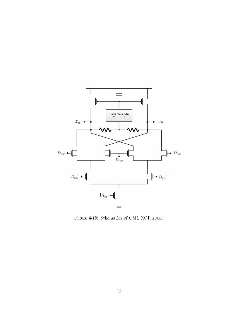
𝑉𝑏𝑛
𝑧𝑛 𝑧𝑝
𝐷𝑖𝑛𝑝 𝐷𝑖𝑛𝑝
𝐷𝑖𝑛𝑝′
𝐷𝑖𝑛𝑛′
𝐷𝑖𝑛𝑛
Common-modeControl
Figure 4-10: Schematics of CML XOR stage.
73

more flexible in a dense C2C network. It also reduces cost of external components
and need for tight tolerances in matching frequencies between received data and
clock. But, to function error-free reference-less receiver needs to adjust clock phase
and frequency to incoming data automatically.
Reference-less receiver in [102] automatically tunes to incoming data using Early/Late
discrepancy index from bang-bang phase detector output to infer frequency offset.
While the receiver in [103] does digital calibration by injecting data edges into a
gated oscillator and observing the phase realignment to infer the frequency offset for
adjustment. Neither of these reference-less receivers injection-lock the oscillator to
the incoming data frequency. In [87], as in this design, the input data edges are
injection-locked into an ILO, and consecutive bang-bang phase detect outputs are
used to discriminate between either phase or frequency update. But, as there is no
frequency error in the injection-lock range, the full lock range could be a "dead-zone"
with equal probability for frequency convergence. The algorithm could end up con-
verging to the edges of the lock range and needs continuous adaptation to avoid losing
lock with supply and temperature drift.
The frequency acquisition algorithm used here runs at startup, but it relies on con-
vergence to the center of the injection-lock range and large lock ranges (unlike [104])
to have tolerance against drift and maintain recovered clock performance metrics
such as 𝐽𝑖𝑡𝑡𝑒𝑟𝑟𝑚𝑠 and JTOL bandwidth. The proposed frequency acquisition loop
uses properties of a conventional bang-bang detector, which based on the sign of the
phase error provides Early (E) or Late (L) information. Consecutive E/L information
is used to determine phase (BB-PD) or frequency (BB-FD) updates into respective
accumulators, as shown in Fig. 4-11. The sequence for frequency acquisition is shown
in Fig. 4-12. Fig. 4-13 shows the circuit details of the MILO-SILO oscillators, where
the natural frequency is set by controlling the reference voltage (𝑣𝑐) of their regulator
and by selecting the switchable load capacitor (𝐶𝐿) at their outputs. At startup the
MILO-SILO oscillators are reset to the lowest frequency using coarse (𝐶𝐿) and fine
(𝑣𝑐) frequency controls. The BB-PD phase control loop is run for a timed interval,
before resetting the error accumulators and running the BB-FD loop and noting the
74

frequency error (𝐹𝑒𝑟𝑟) count. The process is repeated as the frequency control set-
tings (𝐶𝐿, 𝑣𝑐) are swept. The end result is a set of bands of (𝐶𝐿, 𝑣𝑐) settings with 𝐹𝑒𝑟𝑟
counts below a threshold denoting frequency lock. The center of largest such bands
is chosen for its frequency control settings. By choosing the largest band the issue
of harmonic locking is avoided. This setting for MILO-SILO frequency ensures data
is locked in the center of the ILO injection-lock range and latter measurements show
that the lock range is sufficient to ensure tight tolerance for recovered clock 𝐽𝑖𝑡𝑡𝑒𝑟𝑟𝑚𝑠
and JTOL bandwidth over supply and temperature drifts.
If BBPD-based frequency detect logic were to be the sole mechanism to update the
oscillator frequency; then the transition density, jitter, and number of consecutive E or
L signals could all influence the frequency difference between data and the recovered
clock [102]. But, in our scheme BBPD-based frequency detect is run with data-edge
injected into the oscillator, so as to converge on a oscillator frequency setting in the
middle of the largest injection-locked band. Assuming the middle of such a band is
where the free-running frequency of the injection-locked oscillator is closest to 𝑓𝑏𝑎𝑢𝑑/2,
any deviation then is dictated by the quantization of the fine-frequency control (𝑣𝑐)
and is estimated to be of the order of ±20𝑀𝐻𝑧.
4.3.4 Resistively-Interpolated MILO-SILO based Phase-Rotation
Fig. 4-13 shows the circuit details of the MILO-SILO used to achieve high BW for
jitter-tolerance and linearity for the phase rotation of the recovered clock. The natural
frequency of the MILO-SILO oscillators is set by controlling the reference voltage (𝑣𝑐)
of their regulator and by selecting the switchable load capacitor (𝐶𝐿) at their outputs.
The edge-detect output with its strong spectral content at 𝐹𝑏𝑎𝑢𝑑 is injected into the
MILO to achieve injection lock at 𝐹𝑏𝑎𝑢𝑑/2 and leads to high jitter-tolerance BW.
Since the pulling between MILO and SILO is quite strong, the overall lock range
is primarily determined by the coupling between the edge-detect output and the
MILO. Phase calibration of the recovered clock that allows for 360𝑜 phase rotation
is needed for optimal link timing. In this design, phase-shifting at the MILO-SILO
output is achieved by resistively-interpolating between coarse phases (𝑆𝑜 and 𝑆𝑒) from
75

Samplers
Data/EdgeBB-PD
BB-FD
accum.PhaseFreq.Cntrl
EdgeDetect MILO
PhaseRotator
SILO
𝐷𝑖𝑛
𝐹𝑟𝑒𝑞.𝑐𝑛𝑡𝑟𝑙(𝐶𝐿, 𝑣𝑐)
𝑅𝑒𝑐𝑐𝑙𝑘
𝑃ℎ𝑎𝑠𝑒𝑐𝑛𝑡𝑟𝑙
0
1
0
1
0
DataPattern
𝐶𝐿𝐾𝐼
𝐶𝐿𝐾𝑄
E
E
Pair BB-PD
E/E dwn
L/L up
Consecutive E/E
or L/L implies
phase error
0
1
0
1
0
DataPattern
𝐶𝐿𝐾𝐼
𝐶𝐿𝐾𝑄
E
L
Pair BB-FD
E/L up
L/E dwn
Consecutive E/L
or L/E implies
freq. error
Figure 4-11: Shows the use of consecutive early-late transitions to discriminate be-tween and phase and frequency error for tracking and correction.
76

Start reference-less
frequency lock
Step 𝐶𝐿
Step 𝑉𝑐
BB-PD loop
Reset/Run
BB-FD
𝐹𝑒𝑟𝑟 flag
𝑉𝑐 < 𝑙𝑖𝑚𝑖𝑡
𝐶𝐿 < 𝑙𝑖𝑚𝑖𝑡
Select (𝐶𝐿, 𝑉𝑐)
in maximal 𝐹𝑒𝑟𝑟 = 0 band
End
N
N
Y
Y
Figure 4-12: Reference-less frequency lock algorithm which sets the MILO-SILO freerunning frequency to lock in the center of the injection lock range. This ensuresoptimal margin against drift and for jitter-tolerance.
77

the MILO and then injecting the finely interpolated edge (𝑆𝑖𝑛𝑗) into the SILO for
injection lock. Resistive elements are set so that nominally equispaced interpolation
is achieved between 𝑆𝑜 and 𝑆𝑒, while maintaining constant injection strength at 𝑆𝑖𝑛𝑗.
The coarse phase-selections to fine resistive-interpolation settings at different phase-
rotator positions over 2UI is shown in Fig. 4-14. The single-point injection into the
SILO generates multi-phase outputs that are divided down using a set of synchronized-
dividers to generate 𝐹𝑏𝑎𝑢𝑑/4 clocking to the Data and Edge samplers. Unlike prior
ILO-based phase rotators [98, 99] this scheme does not suffer from glitches due to
time-modulated injection or non-linearities due to relying on offsetting the natural
frequency of the SILO to achieve phase-rotation or on mismatch characteristics of
current DACs to achieve linearity.
4.3.5 Clock-less DFE
The CTLE output is fed back through a limiting amplifier (differential gain of 20dB)
and a variable delay buffer (Fig. 4-15), that are also used in the edge-detect block, for
residual first post-cursor equalization. In contrast to [100], this clock-less DFE allows
minimizing the load of the sampling clock and the length of the clock-distribution
tree. The edges from the previous bit at the CTLE output, 𝑑1, transition (𝛼) through
the limiting AMP and replica-delay buffer with a delay window 𝑇𝑑 (shown in blue).
The decision from the feedback applies a post-cursor correction to the current bit 𝑑0
given by, 𝑑0 − 𝑖1.𝑅1𝐴. This assumes the post-cursor weight 𝑖1.𝑅1𝐴 is settled before
the data sampler samples the 𝑑0 bit. Such a settling transition (𝛽) has a settling
window 𝑇𝑠𝑒𝑡𝑡𝑙𝑒 (shown in purple). 𝑇𝑑 and 𝑇𝑠𝑒𝑡𝑡𝑙𝑒 falling within these ranges give the
necessary setup/hold margins for the direct-DFE first post-cursor equalization. The
same frequency-control setting used by the reference-less MILO-SILO is used in the
DFE feedback variable-delay replica-cell to seamlessly meet the setup/hold margins
over a wideband operating range, without complex delay calibration as in [101].
78

𝐶𝐿
𝐶𝐿
𝐶𝐿
𝐶𝐿
𝐶𝐿
𝐶𝐿
𝐶𝐿
𝐶𝐿
𝑆𝐼𝐿𝑂
𝐶𝐿
𝐶𝐿
𝐶𝐿
𝐶𝐿
𝐶𝐿
𝐶𝐿
𝐶𝐿
𝐶𝐿
𝑀𝐼𝐿𝑂
𝑉𝑟𝑒𝑔
0𝑜 45𝑜 90𝑜 135𝑜 180𝑜 225𝑜 270𝑜 315𝑜
8:2 MUX
5r 4r 3r 2r 2r 3r 4r 5r 5r 4r 3r 2r 2r 3r 4r 5r
𝑆𝑖𝑛𝑗
𝑆𝑒 𝑆𝑜
𝐸𝑑𝑔𝑒𝐷𝑒𝑡𝑒𝑐𝑡
𝐹𝑖𝑛𝑒<>
𝐶𝑜𝑎𝑟𝑠𝑒<>
𝐹𝑖𝑛𝑒𝑏<>
Figure 4-13: Master-Slave ILO-based 360𝑜 phase-rotation using resistive-interpolatededges for injection.
79

11111111
𝑆𝑒
𝑆𝑜
0
𝑆𝑖𝑛𝑗
𝐹𝑖𝑛𝑒<>
11111110
𝑆𝑒
𝑆𝑜
1
𝑆𝑖𝑛𝑗
𝐹𝑖𝑛𝑒<>
11111100
𝑆𝑒
𝑆𝑜
2
𝑆𝑖𝑛𝑗
𝐹𝑖𝑛𝑒<>
11111000
𝑆𝑒
𝑆𝑜
3
𝑆𝑖𝑛𝑗
𝐹𝑖𝑛𝑒<>
111100
00
𝑆𝑒
𝑆𝑜 4
𝑆𝑖𝑛𝑗
𝐹𝑖𝑛𝑒<>
111000
00
𝑆𝑒
𝑆𝑜
5𝑆𝑖𝑛𝑗
𝐹𝑖𝑛𝑒<>
11000000
𝑆𝑒
𝑆𝑜
6𝑆𝑖𝑛𝑗
𝐹𝑖𝑛𝑒<>
10000000𝑆𝑒
𝑆𝑜
7
𝑆𝑖𝑛𝑗
𝐹𝑖𝑛𝑒<>
00000000
𝑆𝑒
𝑆𝑜
8
𝑆𝑖𝑛𝑗
𝐹𝑖𝑛𝑒<>
00000001
𝑆𝑒
𝑆𝑜
9
𝑆𝑖𝑛𝑗
𝐹𝑖𝑛𝑒<>
00000011
𝑆𝑒
𝑆𝑜
10
𝑆𝑖𝑛𝑗
𝐹𝑖𝑛𝑒<>
00000111
𝑆𝑒
𝑆𝑜
11
𝑆𝑖𝑛𝑗
𝐹𝑖𝑛𝑒<>
00001111
𝑆𝑒
𝑆𝑜
12
𝑆𝑖𝑛𝑗
𝐹𝑖𝑛𝑒<>
00011111
𝑆𝑒
𝑆𝑜
13
𝑆𝑖𝑛𝑗
𝐹𝑖𝑛𝑒<>
00111111
𝑆𝑒
𝑆𝑜
14
𝑆𝑖𝑛𝑗
𝐹𝑖𝑛𝑒<>
01111111
𝑆𝑒
𝑆𝑜15
𝑆𝑖𝑛𝑗
𝐹𝑖𝑛𝑒<>
11111111
𝑆𝑒
𝑆𝑜
16𝑆𝑖𝑛𝑗
𝐹𝑖𝑛𝑒<>
11111110
𝑆𝑒
𝑆𝑜
17𝑆𝑖𝑛𝑗
𝐹𝑖𝑛𝑒<>
11111100
𝑆𝑒
𝑆𝑜
18
𝑆𝑖𝑛𝑗
𝐹𝑖𝑛𝑒<>
11111000
𝑆𝑒
𝑆𝑜
19
𝑆𝑖𝑛𝑗
𝐹𝑖𝑛𝑒<>
11110000
𝑆𝑒
𝑆𝑜
20
𝑆𝑖𝑛𝑗
𝐹𝑖𝑛𝑒<>
11100000
𝑆𝑒
𝑆𝑜
21
𝑆𝑖𝑛𝑗
𝐹𝑖𝑛𝑒<>
11000000
𝑆𝑒
𝑆𝑜
22
𝑆𝑖𝑛𝑗
𝐹𝑖𝑛𝑒<>
10000000
𝑆𝑒
𝑆𝑜
23
𝑆𝑖𝑛𝑗
𝐹𝑖𝑛𝑒<>
0000
0000
𝑆𝑒
𝑆𝑜
24
𝑆𝑖𝑛𝑗
𝐹𝑖𝑛𝑒<>
00000001 𝑆𝑒
𝑆𝑜
25
𝑆𝑖𝑛𝑗
𝐹𝑖𝑛𝑒<>
00000011
𝑆𝑒
𝑆𝑜
26
𝑆𝑖𝑛𝑗
𝐹𝑖𝑛𝑒<>
000001
11
𝑆𝑒
𝑆𝑜
27 𝑆𝑖𝑛𝑗
𝐹𝑖𝑛𝑒<>
000011
11
𝑆𝑒
𝑆𝑜
28
𝑆𝑖𝑛𝑗
𝐹𝑖𝑛𝑒<>
00011111
𝑆𝑒
𝑆𝑜
29
𝑆𝑖𝑛𝑗
𝐹𝑖𝑛𝑒<>
00111111
𝑆𝑒
𝑆𝑜
30
𝑆𝑖𝑛𝑗
𝐹𝑖𝑛𝑒<>
01111111
𝑆𝑒
𝑆𝑜
31
𝑆𝑖𝑛𝑗
𝐹𝑖𝑛𝑒<>
11111111
𝑆𝑒
𝑆𝑜
32
𝑆𝑖𝑛𝑗
𝐹𝑖𝑛𝑒<>
11111110
𝑆𝑒
𝑆𝑜
33
𝑆𝑖𝑛𝑗
𝐹𝑖𝑛𝑒<>
11111100
𝑆𝑒
𝑆𝑜
34
𝑆𝑖𝑛𝑗
𝐹𝑖𝑛𝑒<>
11111000
𝑆𝑒
𝑆𝑜
35
𝑆𝑖𝑛𝑗
𝐹𝑖𝑛𝑒<>
11110000
𝑆𝑒
𝑆𝑜
36
𝑆𝑖𝑛𝑗
𝐹𝑖𝑛𝑒<>
11100000
𝑆𝑒
𝑆𝑜
37
𝑆𝑖𝑛𝑗
𝐹𝑖𝑛𝑒<>
11000000
𝑆𝑒
𝑆𝑜38
𝑆𝑖𝑛𝑗
𝐹𝑖𝑛𝑒<>
10000000
𝑆𝑒
𝑆𝑜
39𝑆𝑖𝑛𝑗
𝐹𝑖𝑛𝑒<>
00000000
𝑆𝑒
𝑆𝑜
40
𝑆𝑖𝑛𝑗
𝐹𝑖𝑛𝑒<>
00000001
𝑆𝑒
𝑆𝑜
41
𝑆𝑖𝑛𝑗
𝐹𝑖𝑛𝑒<>
00000011
𝑆𝑒
𝑆𝑜
42
𝑆𝑖𝑛𝑗
𝐹𝑖𝑛𝑒<>
00000111
𝑆𝑒
𝑆𝑜
43
𝑆𝑖𝑛𝑗
𝐹𝑖𝑛𝑒<>
00001111
𝑆𝑒
𝑆𝑜
44
𝑆𝑖𝑛𝑗
𝐹𝑖𝑛𝑒<>
00011111
𝑆𝑒
𝑆𝑜
45
𝑆𝑖𝑛𝑗
𝐹𝑖𝑛𝑒<>
00111111
𝑆𝑒
𝑆𝑜
46
𝑆𝑖𝑛𝑗
𝐹𝑖𝑛𝑒<>
01111111
𝑆𝑒
𝑆𝑜47
𝑆𝑖𝑛𝑗
𝐹𝑖𝑛𝑒<>
11111111
𝑆𝑒
𝑆𝑜
48𝑆𝑖𝑛𝑗
𝐹𝑖𝑛𝑒<>
11111110𝑆𝑒
𝑆𝑜
49𝑆𝑖𝑛𝑗
𝐹𝑖𝑛𝑒<>
11111100𝑆𝑒
𝑆𝑜
50
𝑆𝑖𝑛𝑗
𝐹𝑖𝑛𝑒<>
11111000
𝑆𝑒
𝑆𝑜
51
𝑆𝑖𝑛𝑗
𝐹𝑖𝑛𝑒<>
11110000
𝑆𝑒
𝑆𝑜
52
𝑆𝑖𝑛𝑗
𝐹𝑖𝑛𝑒<>
11100000
𝑆𝑒
𝑆𝑜
53
𝑆𝑖𝑛𝑗
𝐹𝑖𝑛𝑒<>
11000000
𝑆𝑒
𝑆𝑜
54
𝑆𝑖𝑛𝑗
𝐹𝑖𝑛𝑒<>
10000000
𝑆𝑒
𝑆𝑜
55
𝑆𝑖𝑛𝑗
𝐹𝑖𝑛𝑒<>
00000000
𝑆𝑒
𝑆𝑜
56
𝑆𝑖𝑛𝑗
𝐹𝑖𝑛𝑒<>
00000001
𝑆𝑒
𝑆𝑜
57
𝑆𝑖𝑛𝑗
𝐹𝑖𝑛𝑒<>
00000011
𝑆𝑒
𝑆𝑜
58
𝑆𝑖𝑛𝑗
𝐹𝑖𝑛𝑒<>
00000111
𝑆𝑒
𝑆𝑜
59
𝑆𝑖𝑛𝑗
𝐹𝑖𝑛𝑒<>
00001111
𝑆𝑒
𝑆𝑜
60
𝑆𝑖𝑛𝑗
𝐹𝑖𝑛𝑒<>
00011111
𝑆𝑒
𝑆𝑜
61
𝑆𝑖𝑛𝑗
𝐹𝑖𝑛𝑒<>
00111111
𝑆𝑒
𝑆𝑜
62
𝑆𝑖𝑛𝑗
𝐹𝑖𝑛𝑒<>
01111111
𝑆𝑒
𝑆𝑜
63
𝑆𝑖𝑛𝑗
𝐹𝑖𝑛𝑒<>
2UI
over
64-steps
Figure 4-14: Coarse phase-selections to fine resistive-interpolation settings at differentphase-rotator positions over 2UI.
80

𝑔𝑚1𝐴
𝐿𝐴𝑅𝑒𝑝𝑙.𝑏𝑢𝑓
DFE feedback timing𝑑0:𝑃𝑟𝑒𝑠𝑒𝑛𝑡𝑏𝑖𝑡 𝑑1:𝑃𝑟𝑒𝑣.𝑏𝑖𝑡
𝑇𝑑𝛼𝑇𝑠𝑒𝑡𝑡𝑙𝑒
𝛽
𝛼𝛽
. . .to samplersCTLE output . . .
. . .
. . .
...
𝐶𝑐...
to 𝑔𝑚1𝐵
𝑅1𝐴
𝑖1
Shared w. Edge-Det.
Figure 4-15: Clock-less direct-feedback DFE with variable delay replica-cell tied tothe delay elements in ILOs to optimally meet DFE loop timing margins.
81

4.3.6 Jitter-tolerance BW using 𝑑 vs. Δ based time-delay
model
The dual-loop clock-data recovery, one part based on BB-PD and other part based
on edge-based injection-locking into the MILO-SILO combination, is linearized and
shown in Fig. 4-16. 𝐾*, 𝜑*, 𝜑𝑛*, and 𝑄* represent scalar gains, phases, phase noises
and quantization errors, respectively, at different stages in the system. Using the
linearized dual-loop model of the proposed architecture, the transfer function from
input phase (𝜑𝑑𝑎𝑡𝑎) to output phase error (𝜑𝑒𝑟𝑟) can be written as in (4.1).
𝜑𝑒𝑟𝑟
𝜑𝑑𝑎𝑡𝑎
= [1− 𝐾𝐵𝐵𝐾𝐼𝐾𝑃𝑅𝑧−𝑀𝛽2
2(1− 𝑧−1/16)(1− 𝑧−1)− 𝛽1
(1− 𝑧−1)· 𝛽1
(1− 𝑧−1)] (4.1)
Jitter on injected pulses, 𝜑𝑖, at the ILO pulls its phase by 𝜑𝑜(𝜑𝑖), leading to the
next injection pulse having a smaller 𝜑𝑖, as shown in Fig. 4-17. In steady state,
𝜑𝑜 → 0, and the settling behaviour of the phase perturbation, 𝜑𝑖, depends on 𝛽(𝜑𝑖).
Assuming 𝛽1 and 𝛽2 to be the relationship between input injection phase to output
phase (analogous to the slope of 𝑑 vs. Δ in the time-delay model [74]) at MILO
and SILO, respectively; the injection-locked oscillator is represented as a first-order
low-pass filter ( 𝛽<𝑥>
(1−𝑧−1)).
As the BB-PD loop has a low BW in this system, the jitter-tolerance BW of the
dual-loop CDR is mostly determined by 𝛽1 and 𝛽2. Open-loop 𝑑 vs. Δ simulations
are used to generate 𝛽1 and 𝛽2 relationships and used to calculate the jitter-tolerance
as described in Fig. 4-18. Comparing the JTOL plot from model based calculations
to actual closed-loop spectre model based simulations shows good correlation and
validates the time-delay models’ usefulness in predicting dynamics of injection-locked
oscillators in tracking input phase deviations.
82

Samplers 𝐾𝐵𝐵𝐾𝐼
1−𝑧−1/16 𝑧−𝑀
×2𝛽1
1−𝑧−1
𝐾𝑃𝑅
𝛽21−𝑧−1 /2
bb-pd
milo ph. rot. silo
𝜑𝑑𝑎𝑡𝑎
𝜑𝑛𝑑𝑎𝑡𝑎
𝜑𝑛𝑚𝑖𝑙𝑜 𝑄𝑃𝑅 𝜑𝑛𝑠𝑖𝑙𝑜
𝜑𝑒𝑟𝑟
High BW loop
Figure 4-16: Discrete-time model of the dual-loop clock-data recovery loop.
𝜑𝑖 Phase Perturbation
𝜑𝑖𝑛𝑗
𝐼𝐿𝑂𝑜𝑢𝑡
𝜑𝑜
𝛽(𝜑𝑖) =𝑑𝜑𝑜𝑑𝜑𝑖
𝛽(𝜑𝑖)(d vs. Δ)
𝑇2
-𝜑𝑖 𝜑𝑜
fn of 𝛽(𝜑𝑖)
Settling a
Figure 4-17: Relationship between input injection phase perturbation and outputphase change and its impact on settling time constant.
83

𝛽(𝜑𝑖)(d vs. Δ)
𝑇2
-𝜑𝑖 𝜑𝑜
𝛽1
MILO
𝛽(𝜑𝑖)(d vs. Δ)
𝑇2
-𝜑𝑖 𝜑𝑜
𝛽2
SILO
𝜑𝑖𝑛𝑗
𝜑𝑓𝑚
1010 pattern
with fm-modulation𝜑𝑒𝑟𝑟JTOL
0 1 2 3 4 5
·108
0.5
1
1.5
2
2.5
Frequency (MHz)
JTOL
(𝑈𝐼 𝑝
𝑝)
𝑆𝑖𝑚𝐶𝑎𝑙.
Figure 4-18: Open-loop 𝑑 vs. Δ values of MILO-SILO used to calculate JTOL andcompared against closed-loop simulations.
84

4.4 Measurements
4.4.1 Experimental Setups
The RX test-chip (Fig. 4-19) was fabricated in 14nm CMOS, with a core RX area of
225𝜇𝑚 x 275𝜇𝑚. A general setup for measurements is shown in Fig. 4-20. Data is
generated in J-BERT N4903B and multiplied up using N4876A 2:1 multiplexer. The
data then goes through a Megtron6 PCB before entering the device under test (D.U.T)
on the probe station. Serial-scan interface is controlled using National Instruments
NI-2162 digital I/O accessory and NI PXI-1042, which is also used to interface with
LabView GUI. Fig. 4-21, shows the setup used to measure the rotator INL/DNL. 1010
data pattern from the J-Bert is multiplied up using N4870A 2:1 Mux to injection-lock
into the MILO-SILO in the D.U.T. The MILO-SILO phase-rotator output recovered
clock from D.U.T is pattern-locked to a trigger in DCA-X 86100D sampling scope.
MILO-SILO phase-rotator is rotated and its phase-step is calculated with reference
to the previous waveform in scope memory.
4.4.2 MILO-SILO, Phase Rotation and Recovered Clock
Fig. 4-22(a-b) shows the measured lock-range of the MILO-SILO recovered clock as a
function of the baud rate with 1010 and PRBS7 patterns, for few discrete frequency
control voltages (𝑣𝑐) and switchable load capacitance (𝐶𝐿) values. The lock-range
is close to 7% of the baud rate. The apparent gaps in the plot are an artifact of
discrete control voltages used in the measurements to show the wideband range of
the frequency lock. With finer frequency control voltage values the plot shows a
continuum of lock-range between 8-19Gb/s. Fig. 4-23 shows the DNL and INL for the
MILO-SILO based phase-rotator over the extreme ends of the performance range (8-
19Gb/s), using the setup shown in Fig. 4-21. With one rotator step corresponding to
1/32 of an UI, the INL of < 1-LSB shows good linearity for the resistive-interpolative
injection based 360𝑜 phase rotation.
Fig. 4-24, shows a typical random jitter measurement for the recovered clock. It
85

275𝜇m
225𝜇m
CTLE
SAMP
MILO-SILO
Deser
BB-PFD
DFE
EDET
VREG
Figure 4-19: Fabricated chip micrograph and layout.
86

D.U.T
N4876A
N4903B
NI PXIMEG6
Figure 4-20: Measurement setup of the DUT. Data is generated in J-BERT N4903Band multiplied up using N4876A 2:1 multiplexer. The data then goes through aMegtron6 PCB before entering the DUT on the probe station. Serial-scan interfaceis controlled using National Instruments NI-2162 digital I/O accessory and NI PXI-1042, which is also used to interface with LabView GUI.
87

D.U.TRec. Clock
Data In
Figure 4-21: Shows the setup used to measure the rotator INL/DNL. 1010 datapattern from the J-Bert is multiplied up using N4870A 2:1 Mux to injection-lock intothe MILO-SILO in the device under test (D.U.T). The MILO-SILO phase-rotatoroutput recovered clock from D.U.T is pattern-locked to a trigger in DCA-X 86100Dsampling scope. MILO-SILO phase-rotator is rotated and its phase-step is calculatedwith reference to the previous waveform in scope memory.
includes not only the jitter transfer from the injected data but also the output clock
buffers and driver. Fig. 4-25(a) shows the RJ of the recovered clock for different
injection data rates within the lock range. For most of the lock range the RJ shows
tight tolerance. Fig. 4-25(b) shows that post initial frequency lock calibration as sup-
ply voltage of the MILO-SILO regulator changes by ±5% or as temperature deviates
between 0C and 100C the recovered clock RJ shows less than 20fs of deviation with
no discernible trends. It is likely that any change in injection-lock range and band-
width due to supply/temperature drift still maintains a large enough BW to show no
appreciable change in the net integrated jitter.
88

6 8 10 12 14 16 18 20 22
2
3
4
5
Baudrate (Gb/s)
(a)
𝐹𝑟𝑒𝑐.𝑐𝑙𝑘
(GHz)
6 8 10 12 14 16 18 20 22
2
3
4
5
Baudrate (Gb/s)
(b)
𝐹𝑟𝑒𝑐.𝑐𝑙𝑘
(GHz)
(𝑣𝑐 =*,𝐶𝐿 =*)(𝑣𝑐 =0.575V,𝐶𝐿 =2)(𝑣𝑐 =0.575V,𝐶𝐿 =3)(𝑣𝑐 =0.45V,𝐶𝐿 =1)(𝑣𝑐 =0.45V,𝐶𝐿 =2)(𝑣𝑐 =0.45V,𝐶𝐿 =3)(𝑣𝑐 =0.35V,𝐶𝐿 =0)(𝑣𝑐 =0.35V,𝐶𝐿 =1)(𝑣𝑐 =0.35V,𝐶𝐿 =2)(𝑣𝑐 =0.35V,𝐶𝐿 =3)
Figure 4-22: Lock range of MILO-SILO at different frequency control voltages (𝑣𝑐)and switchable load cap (𝐶𝐿) with (a)1010 pattern. (b) PRBS7 pattern.
89

0 10 20 30 40 50 60
−1
−0.5
0
0.5
1
Rotator Step
(LSB)
dnl-19Gbpsinl-19Gbpsdnl-8Gbpsinl-8Gbps
Figure 4-23: Measured INL/DNL values of the MILO-SILO based phase-rotator overextremes of operating speed.
4.4.3 Receiver Performance
An experimental setup to measure RX performance over a channel is shown in Fig. 4-
20. Over a 20-inch Megtron6 PCB, which has 15dB of loss at 9.5GHz and significantly
distorts a 19Gb/s data eye (Fig. 4-26), the RX recovers error-free (𝐵𝐸𝑅 < 10−12)
19Gb/s PRBS7 data with a horizontal eye opening of 44% (Fig. 4-27). Without DFE,
the eye opening is 22%, showing the benefits of the clock-less direct-DFE scheme. The
JTOL plot at 19Gb/s is shown in Fig. 4-28(a) for a PRBS7 data (at BER of 10−12,
including ISI), giving a CDR BW of 250MHz. Fig. 4-28(b), shows the JTOL BW
change with supply/temperature drift. The JTOL BW remains > 200𝑀𝐻𝑧 with
drift after initial frequency lock calibration.
90
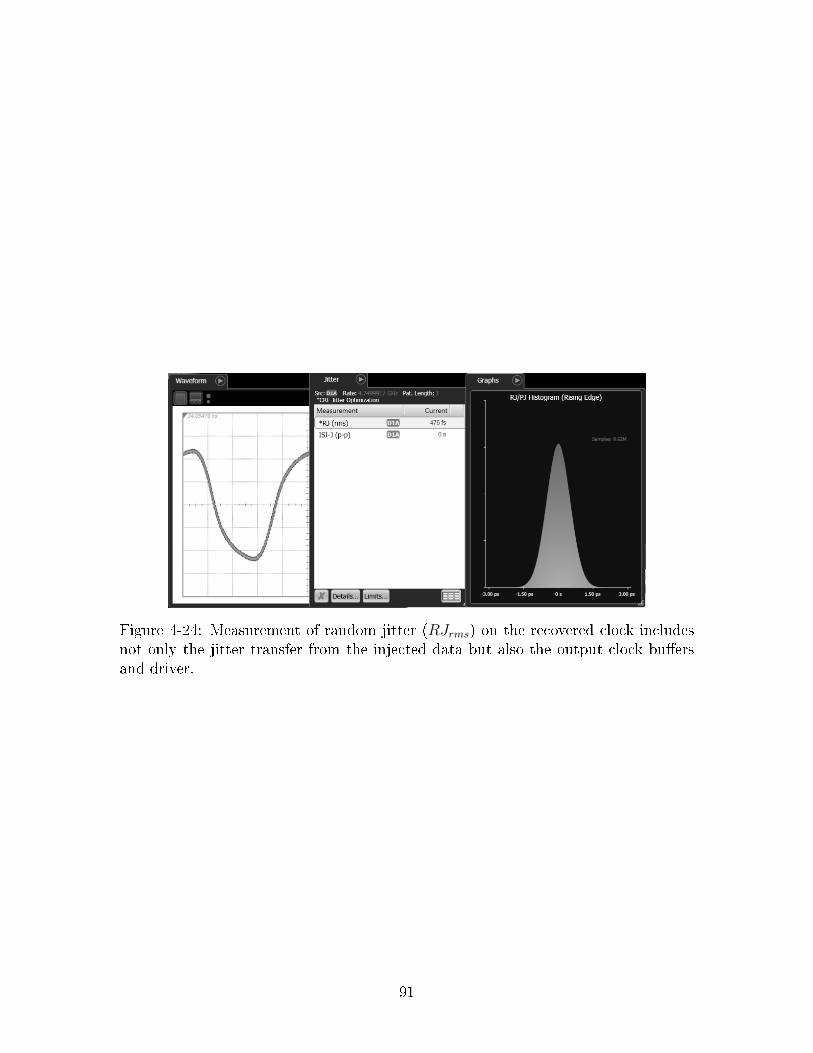
Figure 4-24: Measurement of random jitter (𝑅𝐽𝑟𝑚𝑠) on the recovered clock includesnot only the jitter transfer from the injected data but also the output clock buffersand driver.
91
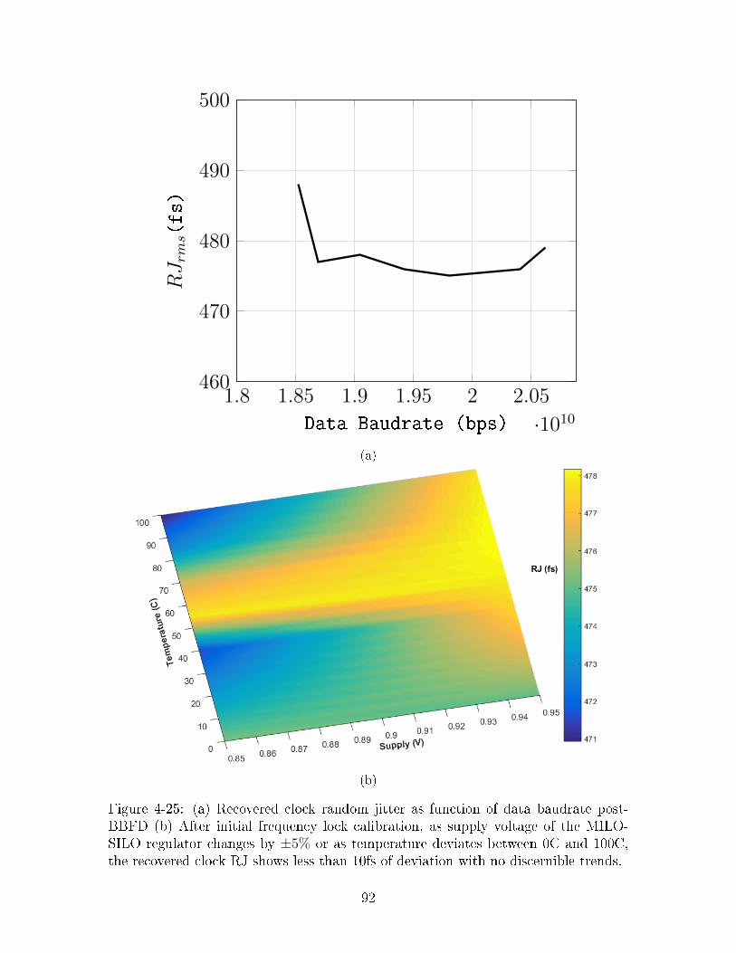
1.8 1.85 1.9 1.95 2 2.05
·1010460
470
480
490
500
Data Baudrate (bps)
𝑅𝐽𝑟𝑚𝑠(fs)
(a)
(b)
Figure 4-25: (a) Recovered clock random jitter as function of data baudrate post-BBFD (b) After initial frequency lock calibration, as supply voltage of the MILO-SILO regulator changes by ±5% or as temperature deviates between 0C and 100C,the recovered clock RJ shows less than 10fs of deviation with no discernible trends.
92
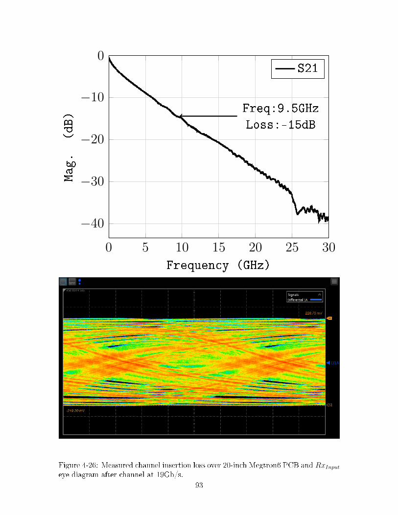
0 5 10 15 20 25 30
−40
−30
−20
−10
0
Frequency (GHz)
Mag.
(dB)
S21
Freq:9.5GHz
Loss:-15dB
Figure 4-26: Measured channel insertion loss over 20-inch Megtron6 PCB and 𝑅𝑥𝐼𝑛𝑝𝑢𝑡
eye diagram after channel at 19Gb/s.
93

−0.4 −0.2 0 0.2 0.4
−12
−10
−8
−6
−4
UI
𝐿𝑜𝑔
10(BER)
pk=12 𝐼𝑑𝑓𝑒 = 0𝜇𝐴pk=6 𝐼𝑑𝑓𝑒 = 20𝜇𝐴pk=6 𝐼𝑑𝑓𝑒 = 0𝜇𝐴
44% @ 10−12
Figure 4-27: RX performance at 19Gbps over 20-inch MEG6 channel.
94

100 101 10210−1
100
101
Frequency (MHz)
JTOL
(𝑈𝐼 𝑝
𝑝)
Equipment limitation
JTOL BW: > 200MHz
(a)
0 20 40 60 80 100
180
200
220
240
Temperature (C)
JTOLBW(MHz)
(b)
Figure 4-28: (a)Measured JTOL BW at 19Gb/s for PRBS7 data at BER of 10−12
over a 10dB loss channel (b) JTOL BW as a funtion of temperature variation afterfrequency lock calibration.
95

4.4.4 Performance summary and comparison
Other RX performance data are also given in Table 4.2. Fig. 4-29, shows the distri-
bution of the power consumption over different macros in the RX.
Table 4.2: Summary of receiver performance.
Item Description Value
1 Technology 14nm CMOS
2 Data Rate 8-19Gb/s
3 RX Architecture 1-stage Peaking Amp, Quarter-rateClock-less DFE, ILO-CDR
4 CDR JTOL bandwidth > 200MHz
5 Input Swing 450mVppd
6 Channel loss @ Nyquist ∼15dB7 Horizontal Eye Opening @BER 10−12 44% (19Gb/s PRBS7 data pattern)
8 Area 225𝜇𝑚 x 275𝜇𝑚
9 Power @19Gb/s 56mW
10 FOM(pJ/b/dB of loss) @19Gb/s 0.29pJ/b/dB
11 Supply Voltages 0.9V
Table 4.3 shows state of art comparison of energy-efficient interconnect for C2C
applications. Reference [87] uses an reference-less embedded-clocking based design. It
shows >200MHz JTOL BW, which is comparable power to this work. But, this work
has 1.5x the maximum speed while equalizing channels with 3x the loss @ Nyquist.
Reference [105] design requires reference clock and is PLL based requiring clock-
tree planning, both of which constrain an extreme-scale system with high-density
of C2C communication. Even though the operating speed of this design is slightly
higher at 20Gb/s, its CDR BW is 20-times slower at <10MHz compared to this
work. Reference [106] design uses a source-synchronous forwarded-clock approach.
Even though it shows better power-efficiency at lower operating-speeds, in extreme-
scale systems with extreme-density of links this approach would be challenged by
clock-tree planning and EMI. Like [106], reference [107] also uses a source-synchronous
forwarded-clock approach. It shows better power-efficiency at lower operating-speeds.
As with [106], this approach would be challenged by clock-tree planning and EMI in
96

Data-Edge Qtrs8.8%
Custom Logic10%
Edge Detect(DFE)15.7%
CTLE(Datapath)19.5%
Clock Dist.10.1%
MILO18.2%
SILO17.7%
Figure 4-29: Power consumption distribution in the RX.
extreme-scale systems. Even though [107] quotes a CDR BW of 25-300MHz, the
source-synchronous nature of this link would mean that SSC loses its efficiency in
suppressing EMI, when say millions of threads in a dense extreme-scale system are
all synchronous to each other. Comparing the design against other designs with
reference-less clock-data recovery units, as seen in Fig. 4-30, shows this receiver to be
having the best FoM when considering the operating speed, channel loss @ Nyquist
and the JTOL bandwidth. In summary, this work stands out when one considers the
problem it is solving. By avoiding need for reference-clock and complex clock-tree it
simplifies clock planning in dense extreme scale systems. Also by maintaining large
jitter tracking bandwidths it enables use of SSC for EMI. Other enhancements such as
master-slave ILO-based phase-rotation and clock-less DFE improve Rx equalization
performance in a power-efficient manner.
97

Table 4.3: State of art comparison of energy-efficient dense VSR-C2C interconnects
Item Description This Work [41] [105]
1 Technology (CMOS) 14nm 28nm 28nm
2 Data Rate (Gb/s) 8-19 1-12 20
3 Clocking Arch. 𝑅𝑒𝑓𝑙𝑒𝑠𝑠-embedded 𝑅𝑒𝑓𝑙𝑒𝑠𝑠-embedded w. Ref.,Pll-based𝑎𝑠𝑦𝑛𝑐4 Jitter tracking bandwidth > 200MHz > 200MHz < 10MHz
5 Input Swing (𝑚𝑉𝑝𝑝𝑑) 450 400 —
6 Channel loss @ Nyquist (dB) 15 5 20
7 Power Efficiency (pJ/b) 2.9 2.8 6.5
8 Supply Voltages 0.9V 0.9V 1.35V/0.9V
→ cont’d This Work [106] [107]
1 Technology (CMOS) 14nm 32nm 65nm
2 Data Rate (Gb/s) 8-19 12 4-7.4
3 Clocking Arch. 𝑅𝑒𝑓𝑙𝑒𝑠𝑠-embedded 𝑆𝑜𝑢𝑟𝑐𝑒𝑠𝑦𝑛𝑐-𝑓𝑜𝑟𝑤𝑎𝑟𝑑𝑒𝑑𝑐𝑙𝑘 𝑆𝑜𝑢𝑟𝑐𝑒𝑠𝑦𝑛𝑐-𝑓𝑜𝑟𝑤𝑎𝑟𝑑𝑒𝑑𝑐𝑙𝑘4 Jitter tracking bandwidth > 200MHz — 25-300MHz
5 Input Swing (𝑚𝑉𝑝𝑝𝑑) 450 400 —
6 Channel loss @ Nyquist (dB) 15 14 5
7 Power Efficiency (pJ/b) 2.9 1.9 0.92
8 Supply Voltages 0.9V — —
100 101 102
10
20
30
40
[87]
[This-work]
[102]
[108]
[109][110]
[111]
JTOL at 1𝑈𝐼𝑝𝑝 (MHz)
Speed(G
bps)
10−1 100 101 1020
2
4
6
[87][This-work][102]
[108]
[109]
[110]
[111]
JTOL at 1𝑈𝐼𝑝𝑝 (MHz)
FoM
(𝑚𝑊
𝐺𝑏𝑝𝑠+
𝐼𝐿𝑑𝐵)
Figure 4-30: Comparison of RX CDR bandwidth, speed, power efficiency, and channelloss at Nyquist against other reference-less clock-data recovery designs.
98

4.5 Summary
This chapter presented a reference-less receiver architecture using embedded-oscillators
having high jitter tolerance bandwidth for VSR-C2C channels. This receiver is shown
to be 1.5x faster than previous reference-less embedded-oscillator based designs with
greater than 100MHz jitter tolerance bandwidth while recovering error-free data over
VSR-C2C channels. Reference-less high-bandwidth CDR simplifies clock-tree plan-
ning in dense extreme-scale computing environments and enables SSC for suppressing
EMI and to mitigate TX jitter requirements. Key design features include a linear first
of its kind phase generator/interpolator based on resistively-interpolated master-slave
ILOs, and a clock-less DFE. Clock-less DFE reduces clock-tree load while boosting
signal-to-noise ratio in presence of crosstalk and is implemented seamlessly (no DFE
specific delay calibration) using variable delay information from the embedded-ILO
to maintain optimal DFE loop margins while directly feeding back into the CTLE
output. The RX is implemented in 14nm CMOS and characterized at 19GB/s. It
achieves a power-efficiency of 2.9pJ/b while recovering error-free data (𝐵𝐸𝑅 < 10−12)
across a 15dB loss channel. The jitter tolerance bandwidth of the receiver over
supply/temperature drift is > 200𝑀𝐻𝑧 and INL of the ILO-based phase-rotator
(32𝑆𝑡𝑒𝑝𝑠/𝑈𝐼) is < 1− 𝐿𝑆𝐵.
99

Chapter 5
Conclusion
This thesis presented several new architectures and integrated circuits for the real-
ization of low-power transceivers for extreme-scale systems. In an hierarchical het-
erogeneous interconnect envisioned in extreme-scale systems there is a need for IO
interconnect with diverse requirements. Some IO might have use for embedded clock-
frequency synthesizers functioning off core power supply, other might have low power
area footprint requirements functioning in extreme dense spaces. The architectures
and singular solutions presented in this thesis aim to solve challenges in this diverse
requirement space. The small footprint, low-power, low-supply, high-frequency op-
eration of ILOs make them very attractive for high data rate communication. The
thesis showed how integration of such systems on silicon open up several architec-
tural and circuit possibilities that enable good system performance in non-traditional
ways. Singular performance was demonstrated taking advantage of unique properties
of nonharmonic injection-locked oscillators.
To begin with the thesis develops a delay-based model to predict the injection
locking behavior of non-harmonic oscillators such as ring oscillators. The effect of the
injection signal on the oscillator is modeled with a d versus Δ characteristic which
captures the additional delay d in a stage due to the effect of the injection signal with
a delay Δ. Using this characteristic, the injection-locking range as well as injection-
locking dynamics can be accurately modeled and predicted. This modeling approach
was applied to a differential four-stage ring oscillator where analytical expressions for
100
the waveforms could be derived along with an analytical expression for the d versus
Δ characteristic. Versatility of the modeling approach was demonstrated by ana-
lyzing the locking behavior of a single-ended three-stage CMOS-inverter-based ring
oscillator. In this case the d versus Δ characteristic was derived from simulations
and measurements. By simulating for d versus Δ characteristic, the model is also
applied to predict the lock range of a multi-phase injection-locked ring-oscillator-
based prescaler, as well as the dynamics of tracking injection phase perturbations
in injection-locked master-slave oscillators. The presented time-domain delay-based
modeling approach can be applied to any nonharmonic oscillator as long as the rela-
tionship between the extra delay d and the delay Δ between the injection signal and
the relevant internal oscillator is available.
The thesis then presented a sub-integer clock-frequency synthesizer architecture
that can operate at a high speed from an ultra-low supply. A record speed of 9GHz
has been demonstrated at 0.5V in 45nm SOI CMOS. Key design features are de-
scribed to achieve such high frequencies with fine resolution at an ultra-low supply.
The proposed multi-phase multi-input ILRO-prescaler eliminates the speed bottle-
neck, while automatic injection-lock calibration ensures lock between the VCO and
the ILRO-prescaler. The phase-switching based programmable divider structure pro-
vides fine frequency resolution through sub-integer division. The PLL power/area are
3.5mW and 0.05mm2, RMS jitter is 325fs, yielding a FOM𝐴 of -186.5.
Finally, the thesis describes a receiver with a reference-less clocking architecture for
high-density VSR-C2C links. This architecture simplifies clock-tree planning in dense
extreme-scaling computing environments and has high-bandwidth CDR to enable
SSC for suppressing EMI and to mitigate TX jitter requirements. Several circuit
and architecture features have been described, including a phase rotator based on
resistively-interpolated injection-locked oscillator with < 1 − 𝐿𝑆𝐵 INL, a clock-less
DFE, and a high-BW JTOL with reference-less frequency lock. Measured results
show 19Gb/s link operation over channels with up to 15dB of loss at Nyquist, while
achieving a power efficiency of 2.9pJ/bit. The reported reach and power efficiency
demonstrate the suitability of this architecture for power critical high-density I/O
101

applications with short reach, as required for future high-performance extreme-scale
systems.
5.1 Future Research
The sub-integer clock-frequency synthesizer and reference-less receiver using embedded-
oscillators have been demonstrated to be robust against drift with startup calibration.
With the scaling in CMOS technologies and potentially larger process variation and
temperature sensitivities, it would be useful research avenue to introduce dynamic
calibration and adaptation into the designs. There are also potential benefits in ex-
tending this clock-frequency synthesis architecture into fractional-N space. Compared
to a conventional multi-modulo divider following the ILRO-prescaler, the sub-integer
division architecture shown in this thesis if used in a ultra-low supply fractional-N
PLL would have the effect of reducing quantization noise by 15.5dB. Another poten-
tial avenue for research is energy-proportional operation of serial links for realizing
energy-efficient data centers. Burst-mode communication, where the link is powered-
off when idle and powered-on when needed, achieves energy proportional operation.
The main challenges in achieving small power-on time and off-state power include the
design of fast-locking PLLs, CDRs and achieving fast settling of bias node voltages.
The reference-less embedded-clock scheme shown in this thesis could be improved on
to meet these power-on time challenges for potential use in burst-mode communica-
tion.
102

Bibliography
[1] P. Kogge et al., "ExaScale Computing Study: Technology Challenges in Achiev-ing Exascale Systems", ExaScale Study Group, 2008.
[2] G. Yeric, "Moore’s Law at 50: Are we planning for retirement?", IEEE Inter-national Electron Devices Meeting (IEDM), 2015.
[3] S. Borkar, "The Exascale challenge", Proceedings of 2010 International Sympo-sium on VLSI Design, Automation, and Test, 2010.
[4] P. Kogge et al., "Facing the Exascale Energy Wall", International Workshopon Innovative Architecture for Future Generation High-Performance Processorsand Systems, 2010.
[5] H. Wu et al., "A 19GHz 0.5mW 0.35𝜇m CMOS Frequency Divider with Shunt-Peaking Locking-Range Enhancement", IEEE International Solid-State Cir-cuits Conf., 2001.
[6] K. Yamamoto et al., "70GHz CMOS Harmonic Injection-Locked Divider",IEEE International Solid-State Circuits Conf., 2006.
[7] H. Wu et al., "A 16-to-18GHz 0.18𝜇m Epi-CMOS Divide-by-3 Injection-LockedFrequency Divider", IEEE International Solid-State Circuits Conf., 2006.
[8] P. Mayr et al., "A 90GHz 65nm CMOS Injection-Locked Frequency Divider",IEEE International Solid-State Circuits Conf., 2007.
[9] S. Rong et al., "0.9mW 7GHz and 1.6mW 60GHz Frequency Dividers withLocking-Range Enhancement in 0.13𝜇m CMOS", IEEE International Solid-State Circuits Conf., 2009.
[10] B.-Y. Lin et al., "A 128.24-to-137.00GHz Injection-Locked Frequency Dividerin 65nm CMOS", IEEE International Solid-State Circuits Conf., 2009.
[11] H.-K. Chen et al., "A mm-Wave CMOS Multimode Frequency Divider", IEEEInternational Solid-State Circuits Conf., 2009.
[12] Z. Huang et al., "A 70.5-to-85.5GHz 65nm Phase-Locked Loop with PassiveScaling of Loop Filter", IEEE International Solid-State Circuits Conf., 2015.
103

[13] S.Y. Yue et al., "A 17.1 to 17.3GHz Image-Reject Down-Converter with Phase-Tunable LO Using 3x Subharmonic Injection Locking", IEEE InternationalSolid-State Circuits Conf., 2004.
[14] S.D. Toso et al., "UWB Fast-Hopping Frequency Generation Based on Sub-Harmonic Injection Locking", IEEE International Solid-State Circuits Conf.,2008.
[15] W.L. Chan et al., "A 56-to-65GHz Injection-Locked Frequency Tripler withQuadrature Outputs in 90nm CMOS", IEEE International Solid-State CircuitsConf., 2008.
[16] A. Mazzanti et al., "A 13.1% Tuning Range 115GHz Frequency Generator Basedon an Injection-Locked Frequency Doubler in 65nm CMOS", IEEE Interna-tional Solid-State Circuits Conf., 2010.
[17] D. Shin et al., "A Mixed-Mode Injection Frequency-Locked Loop for Self-Calibration of Injection Locking Range and Phase Noise in 0.13𝜇m CMOS",IEEE International Solid-State Circuits Conf., 2016.
[18] M.-J.E. Lee et al., "A Second-Order Semi-Digital Clock Recovery Circuit Basedon Injection Locking", IEEE International Solid-State Circuits Conf., 2003.
[19] F. O’Mahony et al., "10GHz Clock Distribution Using Coupled Standing-WaveOscillators", IEEE International Solid-State Circuits Conf., 2003.
[20] F. O’Mahony et al., "A 27Gb/s Forwarded-Clock I/O Receiver Using anInjection-Locked LC-DCO in 45nm CMOS", IEEE International Solid-StateCircuits Conf., 2008.
[21] M. Hossain et al., "A 6.8mW 7.4Gb/s Clock-Forwarded Receiver with up to300MHz Jitter Tracking in 65nm CMOS", IEEE International Solid-State Cir-cuits Conf., 2010.
[22] J.-H. Seol et al., "An 8Gb/s 0.65mW/Gb/s Forwarded-Clock Receiver Usingan ILO with Dual Feedback Loop and Quadrature Injection Scheme", IEEEInternational Solid-State Circuits Conf., 2013.
[23] M. Raj et al., "A 4-to-11GHz Injection-Locked Quarter-Rate Clocking for anAdaptive 153fJ/b Optical Receiver in 28nm FDSOI CMOS", IEEE Interna-tional Solid-State Circuits Conf., 2015.
[24] J. Lee et al., "Subharmonically Injection-Locked PLLs for Ultra- Low-NoiseClock Generation", IEEE International Solid-State Circuits Conf., 2009.
[25] P. Park et al., "An All-Digital Clock Generator Using a Fractionally Injection-Locked Oscillator in 65nm CMOS", IEEE International Solid-State CircuitsConf., 2012.
104

[26] Y.-C. Huang et al., "A 2.4GHz Sub-Harmonically Injection-Locked PLL WithSelf-Calibrated Injection Timing", IEEE International Solid-State CircuitsConf., 2012.
[27] W. Deng et al., "A 0.022mm2 970𝜇W Dual-Loop Injection-Locked PLL with-243dB FOM Using Synthesizable All-Digital PVT Calibration Circuits", IEEEInternational Solid-State Circuits Conf., 2013.
[28] I.-T. Lee et al., "A Divider-Less Sub-Harmonically Injection-Locked PLL withSelf-Adjusted Injection Timing", IEEE International Solid-State Circuits Conf.,2013.
[29] J.-C. Chien et al., "A Pulse-Position-Modulation Phase-Noise-Reduction Tech-nique for a 2-to-16GHz Injection-Locked Ring Oscillator in 20nm CMOS", IEEEInternational Solid-State Circuits Conf., 2014.
[30] W. Deng et al., "A 0.048mm2 3mW Synthesizable Fractional-N PLL with a SoftInjection-Locking Technique", IEEE International Solid-State Circuits Conf.,2015.
[31] A. Elkholy et al., "A 6.75-to-8.25GHz 2.25mW 190𝑓𝑠𝑟𝑚𝑠 Integrated-JitterPVT-Insensitive Injection-Locked Clock Multiplier Using All-Digital Continu-ous Frequency-Tracking Loop in 65nm CMOS", IEEE International Solid-StateCircuits Conf., 2015.
[32] A. Elkholy et al., "A 6.75-to-8.25GHz, 250𝑓𝑠𝑟𝑚𝑠-Integrated-Jitter 3.25mWRapid On/Off PVT-Insensitive Fractional-N Injection-Locked Clock Multiplierin 65nm CMOS", IEEE International Solid-State Circuits Conf., 2016.
[33] D. Coombs et al., "A 2.5-to-5.75GHz 5mW 0.3𝑝𝑠𝑟𝑚𝑠-Jitter Cascaded Ring-BasedDigital Injection-Locked Clock Multiplier in 65nm CMOS", IEEE InternationalSolid-State Circuits Conf., 2017.
[34] S. Yoo et al., "A PVT-Robust -39dBc 1kHz-to-100MHz Integrated- Phase-Noise 29GHz Injection-Locked Frequency Multiplier with a 600𝜇W Frequency-Tracking Loop Using the Averages of Phase Deviations for mm-Band 5GTransceivers", IEEE International Solid-State Circuits Conf., 2017.
[35] H.C. Ngo et al., "A 0.42ps-Jitter -241.7dB-FOM Synthesizable Injection-LockedPLL with Noise-Isolation LDO", IEEE International Solid-State Circuits Conf.,2017.
[36] A. Hussein et al., "A 50-to-66GHz 65nm CMOS All-Digital Fractional-N PLLwith 220𝑓𝑠𝑟𝑚𝑠 Jitter", IEEE International Solid-State Circuits Conf., 2017.
[37] S. Kim et al., "A 2.5GHz Injection-Locked ADPLL with 197fs𝑟𝑚𝑠 IntegratedJitter and -65dBc Reference Spur Using Time-Division Dual Calibration", IEEEInternational Solid-State Circuits Conf., 2017.
105

[38] S. Yoo et al., "A PVT-Robust -39dBc 1kHz-to-100MHz Integrated- Phase-Noise 29GHz Injection-Locked Frequency Multiplier with a 600𝜇W Frequency-Tracking Loop Using the Averages of Phase Deviations for mm-Band 5GTransceivers", IEEE International Solid-State Circuits Conf., 2017.
[39] J. Terada et al., "Jitter-Reduction and Pulse-Width-Distortion CompensationCircuits for a 10Gb/s Burst-Mode CDR Circuit", IEEE International Solid-State Circuits Conf., 2009.
[40] K. Maruko et al., "A 1.296-to-5.184Gb/s Transceiver with 2.4mW/(Gb/s)Burst-mode CDR using Dual-Edge Injection-Locked Oscillator", IEEE Inter-national Solid-State Circuits Conf., 2010.
[41] T. Masuda et al., "A 12Gb/s 0.9mW/Gb/s Wide-Bandwidth Injection- TypeCDR in 28nm CMOS with Reference-Free Frequency Capture", IEEE Interna-tional Solid-State Circuits Conf., 2016.
[42] K. Schier et al., "A 57-to-66GHz Quadrature PLL in 45nm Digital CMOS",IEEE International Solid-State Circuits Conf., 2009.
[43] K.-T. Tsai et al., "A 43.7mW 96GHz PLL in 65nm CMOS", IEEE InternationalSolid-State Circuits Conf., 2009.
[44] K. Kawasaki et al., "A Millimeter-Wave Intra-Connect Solution", IEEE Inter-national Solid-State Circuits Conf., 2010.
[45] S.-J. Cheng et al., "A 110pJ/b Multichannel FSK/GMSK/QPSK/4-DQPSKTransmitter with Phase-Interpolated Dual-Injection DLL-Based SynthesizerEmploying Hybrid FIR", IEEE International Solid-State Circuits Conf., 2013.
[46] K. Kamogawa, T. Tokumitsu, and M. Aikawa, "Injection-locked oscillator chain:a possible solution to millimeter-wave MMIC synthesizers," IEEE Transactionson Microwave Theory and Techniques, vol. 45, pp. 1578-1584, September 1997.
[47] R. A. York and T. Itoh, "Injection and phase locking techniques for beamcontrol," IEEE Transactions on Microwave Theory and Techniques, vol. 46,pp. 1920-1929, November 1998.
[48] S. Verma, H. Rategh, and T. Lee, "A unified model for injection-locked fre-quency dividers," IEEE J. of Solid-State Circuits, vol. 38, no. 6, pp. 1105-1027,2003.
[49] P. Kinget, R. Melville, D. Long, and V. Gopinathan, "An injection-lockingscheme for precision quadrature generation," IEEE J. of Solid-State Circuits,vol. 37, pp. 845-851, July-2002.
[50] R. Adler, "A study of locking phenomena in oscillators," Proc. IEEE, vol. 61,pp. 1380-1385, Oct. 1973.
106

[51] L. J. Paciorek, "Injection locking of oscillators," Proc. IEEE, vol. 53, pp. 1723-1727, Nov. 1965.
[52] B. Razavi, "A study of injection locking and pulling in oscillators," IEEE J. ofSolid-State Circuits, vol. 39, no. 9, Sept. 2004.
[53] M. T. Jezewski, "An approach to the analysis of injection locked oscillators,"in IEEE Transactions on Circuits and Systems, vol. CAS-21, no. 3, May 1974,pp. 395-401.
[54] X. Zhang, X, Zhou, A. S. Daryoush, "A theoretical and experimental studyof the noise behavior of subharmonically injection locked local oscillators," inIEEE Transactions on Microwave Theory and Techniques, vol. 40, no. 5, May1992, pp. 895-902.
[55] X. Lai, J. Roychowdhury, "Capturing oscillator injection locking via nonlinearphase-domain macromodels," in IEEE Transactions on Microwave Theory andTechniques, vol. 52, no. 9, Sept. 2004, pp. 2251-2261.
[56] X. Lai, J. Roychowdhury, "Analytical equation for predicting injection lockingin LC and ring oscillators," in IEEE Custom Integrated Circuits Conf., Sept.2005.
[57] G. R. Gangasani, P. Kinget, "A time-domain model for predicting the injec-tion locking bandwidth of non-harmonic oscillators," in IEEE Transactions onCircuits and Systems II, vol. 53, no. 10, Oct. 2006.
[58] G. R. Gangasani, P. Kinget, "Injection-Lock dynamics in non-harmonicoscillators," in IEEE International Symposium on Circuits and Systems, May2006.
[59] R. J. Betancourt-Zamora, S. Verma, and T. Lee, "1-GHz and 2.8-GHz injection-locked ring oscillator prescalers," in IEEE Symp. VLSI Circuits Dig. Tech. Pa-pers, June 2001, pp. 47-50.
[60] MPQ2222A, NPN silicon quad chip: Central Semiconductor Corp.
[61] CD4007UB, CMOS Dual complementary pair inverter: Texas Instruments.
[62] P. Kogge et al., "ExaScale Computing Study: Technology Challenges in Achiev-ing Exascale Systems", ExaScale Study Group, 2008.
[63] T. Toifl, et al., "A 0.94-ps-RMS-Jitter 0.016mm2 2.5-GHz Multiphase GeneratorPLL with 360𝑜 Digitally Programmable Phase Shift for 10-Gb/s Serial Links",IEEE J. of Solid-State Circuits, vol. 40, no. 12, Dec. 2005.
[64] B. A. Floyd, "Sub-Integer Frequency Synthesis Using Phase-Rotating Fre-quency Dividers", IEEE Transactions on Circuits and Systems I, vol. 55, no. 7,Aug. 2008.
107
[65] P. R. Kinget, "Scaling Analog Circuits into Deep Nanoscale CMOS: Obstaclesand Ways to Overcome Them", IEEE Custom Integrated Circuits Conf., Sept.2015.
[66] A. Paidimarri, N. Ickes and A. P. Chandrakasan, "A 0.68V 0.68mW 2.4GHz PLLfor Ultra-Low Power RF Systems", IEEE Radio Frequency Integrated CircuitsSymposium, May 2015.
[67] S. Ikeda, et al., "A Sub-1mW 5.5-GHz PLL with Digitally-Calibrated ILFD andLinearized Varactor for Low Supply Voltage Operation", IEEE Radio FrequencyIntegrated Circuits Symposium, June 2013.
[68] S. Ikeda, et al., "A 0.5-V 5.5-GHz Class-C-VCO-Based PLL with Ultra-Low-Power ILFD in 65nm CMOS", IEEE Asian Solid-State Circuits Conf., Nov.2012.
[69] S.-A. Yu and P. R. Kinget, "A 0.65V 2.5GHz Fractional-N Frequency Syn-thesizer in 90nm CMOS", IEEE International Solid-State Circuits Conf., Feb.2007.
[70] N. Krishnapura and P. R. Kinget, "A 5.3-GHz Programmable Divider for HiPer-LAN in 0.25-𝜇m CMOS", IEEE J. of Solid-State Circuits, vol. 35, no. 7, July2000.
[71] A. Momtaz, et al., "Fully-Integrated SONET OC48 Transceiver in StandardCMOS", IEEE International Solid-State Circuits Conf., Sept. 2001.
[72] N. H. W. Fong, et al., "A 1-V 3.8-5.7-GHz Wide-Band VCO With Differen-tially Tuned Accumulation MOS Varactors for Common-Mode Noise Rejec-tion in CMOS SOI Technology", IEEE Transactions on Microwave Theory andTechniques, vol. 51, no. 8, Aug. 2003.
[73] J.-K. Kim, et al., "A 26.5-37.5 GHz Frequency Divider and a 73-GHz-BW CMLBuffer in 0.13𝜇m CMOS", IEEE Asian Solid-State Circuits Conf., Nov. 2007.
[74] G. R. Gangasani and P. R. Kinget, "Time-Domain Model for Injection Lockingin Nonharmonic Oscillators", IEEE Transactions on Circuits and Systems I,vol. 55, no. 6, July 2008.
[75] Y.-C. Lo, H.-P. Chen, J. Silva-Martinez and S. Hoyos, "A 1.8V, Sub-mW, Over100% Locking Range, Divide-by-3 and 7 Complementary-Injection-Locked 4GHz Frequency Divider", IEEE Custom Integrated Circuits Conf., Sept. 2009.
[76] G. G. Shahidi, et al., "Device and Circuit Design Issues in SOI Technology",IEEE Custom Integrated Circuits Conf., Sept. 1998.
[77] J.F. Bulzacchelli, et al., "A 28-Gb/s 4-Tap FFE/15-Tap DFE Serial LinkTransceiver in 32-nm SOI CMOS Technology", IEEE J. of Solid-State Circuits,vol. 47, no. 12, Dec. 2012
108
[78] H.-H. Hsieh, C.-T. Lu and L.-H. Lu, "A 0.5-V 1.9-GHz Low-Power Phase-Locked Loop in 0.18-𝜇m CMOS", IEEE Symposium on VLSI Circuits, June2007.
[79] P. Kogge et al., "ExaScale Computing Study: Technology Challenges in Achiev-ing Exascale Systems", ExaScale Study Group, 2008.
[80] P. Kogge et al., "Facing the Exascale Energy Wall", International Workshopon Innovative Architecture for Future Generation High-Performance Processorsand Systems, 2010.
[81] T. Dickson et al., "A 1.4 pJ/bit, Power-Scalable 16x12 Gb/s Source-Synchronous I/O With DFE Receiver in 32 nm SOI CMOS Technology", IEEEJ. of Solid-State Circuits, vol. 50, no. 8, Aug. 2015.
[82] T. Dickson et al., "A 1.8 pJ/bit 16x16 Gb/s Source-Synchronous Parallel Inter-face in 32 nm SOI CMOS with Receiver Redundancy for Link Recalibration",IEEE J. of Solid-State Circuits, vol. 51, no. 8, July 2016.
[83] T. Toifl et al., "A 2.6 mW/Gbps 12.5 Gbps RX With 8-Tap Switched-CapacitorDFE in 32 nm CMOS", IEEE J. of Solid-State Circuits, vol. 47, no. 4, April2012.
[84] M. Hossain et al., "A 6.8mW 7.4Gb/s Clock-Forwarded Receiver with up to300MHz Jitter Tracking in 65nm CMOS", IEEE International Solid-State Cir-cuits Conf., 2010.
[85] Pier Andrea Francese et al., "A 16 Gb/s 3.7 mW/Gb/s 8-Tap DFE Receiver andBaud-Rate CDR With 31 kppm Tracking Bandwidth", IEEE J. of Solid-StateCircuits, vol. 49, no. 11, Nov. 2014.
[86] G.R. Gangasani et al., "A 32 Gb/s Backplane Transceiver With On-Chip AC-Coupling and Low Latency CDR in 32 nm SOI CMOS Technology", IEEE J.of Solid-State Circuits, vol. 49, no. 11, Nov. 2014.
[87] T. Masuda et al., "A 12Gb/s 0.9mW/Gb/s Wide-Bandwidth Injection-TypeCDR in 28nm CMOS with Reference-Free Frequency Capture ", IEEE Inter-national Solid-State Circuits Conf., 2016.
[88] G. Shu et al., "A Reference-Less Clock and Data Recovery Circuit Using Phase-Rotating Phase-Locked Loop", IEEE J. of Solid-State Circuits, vol. 49, no. 4,April 2014.
[89] W. Rahman et al., "A 22.5-to-32Gb/s 3.2pJ/b Referenceless Baud-Rate DigitalCDR with DFE and CTLE in 28nm CMOS ", IEEE International Solid-StateCircuits Conf., 2017.
[90] J. D’Ambrosia, "IEEE 802.3WG Closing Plenary Report, IEEE P802.3bj 100Gb/s Backplane and Copper Cable Task Force", http:www.ieee802.org, 2012.
109
[91] T. Beukema et al., "A 6.4-Gb/s CMOS SerDes Core With Feed-Forward andDecision-Feedback Equalization", IEEE J. of Solid-State Circuits, vol. 40, no.12, Dec. 2005.
[92] V. Stojanovic et al., "Modeling and Analysis of High-speed links ", IEEE Cus-tom Integrated Circuits Conf., 2003.
[93] V. Dmitriev-Zdorov et al., "BER- and COM-Way of Channel-Compliance Eval-uation: What are the Sources of Differences", DesignCon, 2016.
[94] G.R. Gangasani et al., "A 28.05Gb/s Transceiver using Quarter-Rate Triple-Speculation Hybrid-DFE Receiver with Calibrated Sampling Phases in 32nmCMOS", IEEE Symposium on VLSI Circuits, 2017.
[95] B. Casper et al., "Clocking Analysis, Implementation and Measurement Tech-niques for High-Speed Data Links-A Tutorial", IEEE Transactions on Circuitsand Systems I, vol. 56, no. 1, Jan. 2009.
[96] J. Lee et al., "A 20-Gb/s Burst-Mode Clock and Data Recovery Circuit UsingInjection-Locking Technique", IEEE J. of Solid-State Circuits, vol. 43, no. 3,Mar. 2008.
[97] M.L. Schmatz et al., "A 40-Gb/s, Digitally Programmable Peaking LimitingAmplifier with 20-dB Differential Gain in 90-nm CMOS", IEEE Radio Fre-quency Integrated Circuits Symposium, 2006.
[98] M. Aleksic, "A 3.2-GHz 1.3-mW ILO Phase Rotator for Burst-Mode MobileMemory I/O in 28-nm Low-Leakage CMOS", IEEE European Solid-State Cir-cuits Conf., 2014.
[99] F. O’Mahony et al., "A programmable Phase Rotator based on Time-ModulatedInjection-Locking", IEEE Symposium on VLSI Circuits, 2010.
[100] G.R. Gangasani et al., "A 16-Gb/s Backplane Transceiver With 12-Tap CurrentIntegrating DFE and Dynamic Adaptation of Voltage Offset and Timing Driftsin 45-nm SOI CMOS Technology", IEEE J. of Solid-State Circuits, vol. 47, no.8, Aug. 2012.
[101] M. Pozzoni et al., "A 12Gb/s 39dB Loss-Recovery Unclocked-DFE Receiverwith Bi-dimensional Equalization", IEEE International Solid-State CircuitsConf., 2010.
[102] G. Shu et al., "A 4-to-10.5 Gb/s Continuous-Rate Digital Clock and Data Re-covery With Automatic Frequency Acquisition", IEEE J. of Solid-State Cir-cuits, vol. 51, no. 2, Feb. 2016.
[103] C.-F. Liang et al., "A Reference-Free, Digital Background Calibration Tech-nique for Gated-Oscillator-Based CDR/PLL", IEEE Symposium on VLSI Cir-cuits, 2009.
110

[104] A. Elkholy et al., "A 6.75-to-8.25GHz 2.25mW 190𝑓𝑠𝑟𝑚𝑠 Integrated-JitterPVT-Insensitive Injection-Locked Clock Multiplier Using All-Digital Continu-ous Frequency-Tracking Loop in 65nm CMOS", IEEE International Solid-StateCircuits Conf., 2015.
[105] V. Balan et al., "A 130mW 20Gb/s Half-Duplex Serial Link in 28nm CMOS",IEEE International Solid-State Circuits Conf., 2014.
[106] T. Dickson et al., "A 1.4 pJ/bit, Power-Scalable 16x12 Gb/s Source-Synchronous I/O With DFE Receiver in 32 nm SOI CMOS Technology", IEEEJ. of Solid-State Circuits, vol. 50, no. 8, Aug. 2015.
[107] M. Hossain et al., "A 6.8mW 7.4Gb/s Clock-Forwarded Receiver with up to300MHz Jitter Tracking in 65nm CMOS", IEEE International Solid-State Cir-cuits Conf., 2010.
[108] W. Rahman et al., "A 22.5-to-32-Gb/s 3.2-pJ/b Referenceless Baud-Rate Dig-ital CDR With DFE and CTLE in 28-nm CMOS", IEEE J. of Solid-StateCircuits, vol. 52, no. 12, Dec. 2017.
[109] M.S. Jalali et al., "A Reference-Less Single-Loop Half-Rate Binary CDR", IEEEJ. of Solid-State Circuits, vol. 50, no. 9, Sept. 2015.
[110] N. Kocaman et al., "An 8.5-11.5-Gbps SONET Transceiver With ReferencelessFrequency Acquisition", IEEE J. of Solid-State Circuits, vol. 48, no. 8, Aug.2013.
[111] J. Lee et al., "A 20-Gb/s Full-Rate Linear Clock and Data Recovery CircuitWith Automatic Frequency Acquisition", IEEE J. of Solid-State Circuits, vol.44, no. 12, Dec. 2009.
111