architectures and algorithms for with foldable logic blocks · 3.2.1 simple and multiple folding...
TRANSCRIPT

Architectures and Algorithms for Laser-Prograrnrned Gate Arrays with
Foldable Logic Blocks
Jason Helge Anderson
A thesis submitted in conformity with the requirements
for the degree of Master of Applied Science
Graduate Department of Electrical and Cornputer Engineering
University of Toronto
O Copyright by Jason Helge Anderson 1997

395 Wellington Street 395, rue Wellington Ottawa ON K1A ON4 Ottawa ON K I A ON4 Canada Canada
Your h k Votre relerence
Our file Notre rddrence
The author has granted a non- L'auteur a accordé une licence non exclusive licence allowing the exclusive permettant à la National Library of Canada to Bibliothèque nationale du Canada de reproduce, loan, distribute or sel1 reproduire, prêter, distribuer ou copies of this thesis in microform, vendre des copies de cette thèse sous paper or electronic formats. la forme de microfiche/film, de
reproduction sur papier ou sur format électronique.
The author retains ownership of the L'auteur conserve la propriété du copyright in this thesis. Neither the droit d'auteur qui protège cette thèse. thesis nor substantial extracts fiom it Ni la thèse ni des extraits substantiels may be printed or othewise de celle-ci ne doivent être imprimés reproduced without the author's ou autrement reproduits sans son permission. autorisation.

Foldable Logic Blocks
Jason Helge Anderson Master of Applied Science, 1997
Department of Electrical and Cornputer Engineering University of Toronto
Abstract
Laser-programmed gate arrays (LPGAs) represent a new approach to application specific
integrated circuit implementation. An LPGA consists of an array of programmable logic blocks as
well as a programmable interconnection network.
This thesis proposes two new LPGA logic block architectures: foldable PLA-style logic
blocks and foldable Iook-up-table-based logic blocks. The proposed logic bIocks are sirnilar to
those found in cornmercially available field-programmable devices. The term foldable refers to
the fact that the granularity of the logic blocks can be varied. This is achieved using the LPGA
laser disconnect methodology. Custom CAD tools have been developed to map circuits into the
new architectures.
Experimental studies show that LPGAs with foldable logic blocks are more area-efficient
than those based on normal unfoldable logic blocks. The proposed LPGA architectures possess
more predictable timing than an existing, commercially available LPGA.

1 would like to take this opportunity to thank my supervisor Professor Stephen Brown for
his advice, direction, and encouragement. It has been a privilege working with him.
1 would like to thank my friends and colleagues in the EECG, including: Vincent, Jason,
Warren, Ali, Vaughn, Yaska, Khalid, Qiang, Mazen, Jordan, Jeff, Wai, S teve Wilton, Guy, Dan,
Alireza, and Dawi.
1 also wish to express my appreciation for the OGS from the Government of Ontario and
for financial support from Chip Express Corporation.
Thanks to Jack Kouloheris for supplying the DDMAP technology mapper for PLA-style
logic blocks. Thanks to Amir Farrahi for providing the C code for the LUT-based technology
mapper, Level-Map.
1 would like to thank Mary for her friendship and encouragement and for helping me to
explore and enjoy Toronto. 1 also appreciate the efforts of Mary and Steve in assisting me with the
job of editing this thesis. Finally, 1 would like to thank my mother, father, sister, and grandmother
for their support during my graduate studies.

Chapter 1 Introduction ............... .......................... ................................................................ 1
....................................................... 1.1 Introduction to Laser-Programmed Gate Arrays I
1.2 Motivation for this Research Study ....................................................................... 3
.................................................................................................... 1.3 Research Approach 5
................................................................................................... 1.4 Thesis Organization 6
Chapter 2 Background and Previous Work ............................. .. .................................... 8
................................................................................................................ 2.1 Introduction 8
.......................................................................................... 2.2 Logic Block Architecture 8
2.3 PLA-Style Logic Blocks ............................................................................................ 9
........................................................................................... 2.3.1 Previous Research 10
...................................................................................... 2.3.2 Synthesis Techniques 10
..................................................................... 2.3.3 Commercial1 y Available CPLDs 12
.......................................................................... 2.3.3.1 Altera MAX 9000 12
..................................................................... 2.3.3.2 AMD Mach 4 Family 15
......................................................................... 2.4 Look-Up-Table-Based Logic Blocks 17
........................................................................................... 2.4.1 Previous Research 18
...................................................................................... 2.4.2 Synthesis Techniques 19
................................................ 2.4.2.1 LUT-Based Technology Mappers 19
...................................................................................... 2.4.2.2 Level -Map 20
............................................... 2.4.3 Commercial1 y Available LUT-Based FPGAs 21
........................................................................... 2.4.3.1 AlteraFLEX 10K 21
............................................................................... 2.4.3.2 Xilinx XC4000 23
............................................................................... 2.5 Commercially Available LPGAs 26
............................................................................................... 2.5.1 QYHSOO LPGA 26
................................................................................................ 2.5.2 CX200 1 LPGA 27
..................................................................... Chapter 3 Foldable PLAStyle Logic Blocks 29
3.1 Introduction ................................................................................................................ 29
......................................................... 3.2 Foldable PLA-Style Logic Block Architecture 29
........................................................................... 3.2.1 Simple and Multiple Folding 32
3.2.3 Effect of Bipartite Folding on Combined Folding .......................................... 34
.......................................................... 3.2.4 Summary of Architectural Parameters 34
3.3 Synthesis .................................................................................................................. 35
3.3.1 Overview of CAD Flow ................................................................................ 36
................................................................. 3.3.2 Technology Independent Synthesis 37
3.3.3 hooPLA: Technology Mapping for Foldable PLA-Style Logic Blocks .......... 38
3.3.3.1 hooPLA Phase 1: Performing an Optimal Tree Mapping .............. 39
.............................. 3.3.3.2 hooPLA Phase II: Heuristic Partial Collapshg 43
..................................................... 3.3.3.3 hooPLA Phase III: Bin Packing 45
3.3.3.4 Cornparison with Existing Technology Mappers ........................... 46
3.3.4 PLA Folding .................................................................................................... 48
3.3.4.1 Previous Work ................................................................................ 49
3.3.4.2 Approach Used to Perform Bipartite Folding ................................ 49
.......................................... 3.3.4.3 Integrating PLA Folding into hooPLA 55
3.4 Summary .................................................................................................................... 56
............ ........................ Chapter 4 Foldable Look-Up-Table-Based Logic Blocks .... 58
................................................................................................................ 4.1 Introduction 58
...................................... 4.2 Foldable Look-Up-Table-Based Logic Block Architecture 58
4.3 Synthesis .............................................................................................................. 62
4.3.1 Overview of CAD Flow ................................................................................ 63
4.3.2 LUTPack: Technology Mapping for Foldable Look-Up-Table-Based
Logic Blocks ............................................................................................. 64
................................................................................................................... 4.4 Summary 67
Chapter 5 Experimental Results .......................................................................................... 68
5.1 Introduction and Architectural Questions .................................................................. 68
5.2 Experimental Procedure ............................................................................................ 68
5.2.1 Benchmark Circuits ....................................................................................... 68
5.2.2 Area Models ................................................................................................ 69
5.2.3 Chip Area of FoIdabIe PLA-Style Logic Blocks ............................................. 70
.......................... 5.2.4 Chip Area of Foldable Look-Up-Table-Based Logic Blocks 72

5.2.6 Limitations of Area Model .............................................................................. 74
................................ 5.3 Area-Efficiency Results for Foldable PLA-style Logic Blocks 75
5.3.1 The Benefits of Folding ............................................................................ 75
..................................................................................................... 5.3.2 Area Results 78
............ 5.4 Area-Efficiency Results for Foldable Look-Up-Table-Based Logic Blocks 82
5.4.1 The Benefits of Folding ................................................................................ 82
..................................................................................................... 5 .4.2 Area Results 83
..................... 5.5 Predictability Benefits of the Coarse-Grained Foldable Architectures 87
.................................................................................................................... 5.6 Summary 89
Chapter 6 Conclusions ....................................................................................................... 90
........................................................................................................ 6.1 Thesis Summary 90
6.2 Thesis Contributions ........................................................................................... 90
..................................................................................... 6.3 Suggestions for Future Work 92
References ................... ... ................................................................................................ 94
Appendix A List of Benchmark Circuits ............................................................................ 100
..................... Appendix B Pessimistic Area Results ..... .... ................... ............................ 101
.................... Appendix C PLA Layout ...... ............................................................................ 104
Appendix D Parameterized Benchmark Suite ........................................... ...................... 105
............................................................................................................... D . 1 Introduction 105
................................................................................................. D.2 Current Benchmarks 105
....................................................................................... D.3 Parameterized Benchmarks 106
................................................................................ D.4 Synopsys Behavioral Compiler 107
......................................................................................... D.5 Designware Components 110
D.6 Synthesized Circuit Format ..................................................................................... 111
...................................................................................... D.7 Description of Benchmarks 1 1 1
Appendix E Comparing with the CX2001 LPGA ...................................... . . ................ 121

Table 3 . f : Table 3.1:
Table 3.3:
Table 3.4:
Table 5.1:
Table 5.2:
Table 5.3:
Table 5.4:
Table 5.5:
Table A . 1 :
Table D . 1 :
Table E . 1 :
Table E.2:
Foldable PLA-Style Logic Block Architectural Parameters .............................. 35
.................................................................. Heuristic Partial Collapsing Criteria 44
Effect of Controlled Partial Collapsing ........................................................... 46
Cornparison with Existing Technology Mappers ............................................... 48
Average Wire Length and Average Ratios of Maximum to Average
Channel Density ................................................................................................ 74
Normalized Area Results for PLA-Based Architectures .................................... 82
................ Normalized Area for Foldable Look-Up-Table-Based Architectures 85
Normalized Area for Heterogeneous Foldable Look-Up-Table
...................................................................................................... Architectures 86
Average Number of Logic Levels on Circuits' Critical Paths for Several
...................................................................................................... Architectures 88
List of Benchmark Circuits ............................................................................ 100
Solutions to Problems with the MCNC Benchmarks ........................................ 107
................................................................. Comparing Number of Logic Blocks 121
Comparing Number of Connected Pins ............................................................. 122
vii

Figure 1 . 1 :
Figure 1.2:
Figure 1.3:
Figure 2.1 :
Figure 2.2:
Figure 2.3:
Figure 2.4:
Figure 2.5:
Figure 2.6:
Figure 2.7:
Figure 2.8:
Figure 2.9:
LPGA Laser Cutting [CEC96] ......................................................................... 1
...................................... Packing Additional Logic into Foldable Logic Blocks 4
Abstract View of Utilization/Granularity Trade-Off ......................................... 5
PLA Structure .................................................................................................... 9
........................................................... Altera MAX 9000 Architecture [Alte961 13
................................................ Altera MAX 9000 Logic Array Block [Alte961 14
................ Altera MAX 9000 Macrocell and Local LAB Interconnect [Alte961 15
AMD Mach 4 Architecture [AMD96] ............................................................... 16
................................................ Portion of AMD Mach 4 PAL Block [AMD96] 17
Structure of Look-Up-Table ............................................................................ 18
....................................................... Architecture of Altera FLEX 10K [Alte961 22
..................................... Altera FLEX 10K Logic Array Block (LAB) [Alte961 23
....................................................... Figure 2.10. Altera FLEX 10K Logic Element [Alte961 23
......................................................................... Figure 2.1 1 : Architecture of Xilinx XC4000 24
.......................................... Figure 2.12. Xilinx XC4000 Configurable Logic Block [Xili94] 25
Figure 2.13. Portion of XC4000 Routing Architecture [Xili94] ............................................ 26
.............................. Figure 2.14. Architecture and Logic Site of QYH 500 LPGA [CEC96a] 27
Figure 2.15. Portion of QYH 500 Routing Circuitry [Jana95] ............................................... 27
................................... Figure 2.16. CX200 1 Logic Block and Example Function [CEC96a] 28
Figure 3.1 : Example PLA Personality Matrix ...................................................................... 29
Figure 3.2. PLA Column Folding ......................................................................................... 30
Figure 3.3. PLA Row Folding ....................................................................................... 31
Figure 3.4: Combined Folding to Pack Additional Logic into a Foldable PLA-Style
Logic Block ....................... ,., .......................................................................... 32
Figure 3.5. Foldable PLA-Style Logic Block ....................................................................... 35
Figure 3.6. CAD Flow for Mapping Circuits into Foldable PLA-Style Logic Blocks ........ 37
Figure 3.7. Partitioning a DAC into a Forest of Fanout-Free Trees .................................... 39
Figure 3.8. Computation of Feasible Subtree Cost ............................................................ 41

. . . .
Figure 3.10. Maximum Shared Input Bin Packing Algorithm .............................................. 45
.............................................................. Figure 3.1 1 : Mapping a PLA into a Bipartite Graph 50
......................................................... Figure 3.12. Partitioned Bipartite Graph with Foldings 52
................................................................. Figure 3.13. Pseudo-Code for Folding Algorithm 53
.... Figure 3.14. Division of a Folded PLA into Two Smaller PLAs for Subsequent Folding 54
Figure 3.15. Algorithmic Flow of hooPLA ............................................................................ 57
Figure 4.1 :
Figure 4.2:
Figure 4.3:
Figure 4.4:
Figure 4.5:
Figure 4.6:
Figure 4.7:
Figure 4.8:
Figure 5.1 :
Figure 5.2:
Figure 5.3:
Figure 5.4:
Figure 5.5:
Figure 5.6:
Figure 5.7:
Figure 5.8:
Figure 5.9:
......................................................... LUT Programming in LPGA Technology 59
Utilization of LUT Inputs ............................................................................... 59
................................................................................................. FoldabIe 4-LUT 60
FoldabIe 4-LUT with Additional Flexibility ..................................................... 62
Output Circuitry for Foldable LUT-Based Logic Block with
Parameters K = 4 and L = 3 ................................................................................ 62
CAD Flow for Mapping Circuits into Foldable LUT-Based Logic Blocks ....... 63
Covering the Multiplexer Tree ...................................................................... 65
........................................ Pseudo-Code for First-Fit-Decreasing LUT Packing 66
........................................................... Pessimistic and Optimistic Area Models 70
....................................................................................... PLA Layout Floorplan 71
The Benefits of PLA FoIding - Percentage Reduction in Number of
...................................................................................................... Logic Blocks 76
Area Results for Unfoldable PLA-Style Logic BIock
................................................................................. Architectures (Optimistic) 78
Ratio of Row Foldable to Unfoldable Area for PLA-Style
Logic Block Architectures (Optimistic) ............................................................. 79
Ratio of Column Foldable to Unfoldable Area for PLA-Style
............................................................. Logic Block Architectures (Optimistic) 80
Ratio of Combined Foldable to Unfoldable Area for PLA-Style
Logic Block Architectures (Optimistic) .......................................................... 81
The Benefits of LUT Folding - Percentage Reduction in Nurnber of
...................................................................................................... Logic Blocks 83
Ratio of Foldable to Unfoldable Area for LUT-Based Logic Block

. *
Figure B. 1 : Area Results for Unfoldable PLA-Style Logic Block
................................................................................ Architectures (Pessimistic) 1 0 1
Figure B.2: Ratio of Row Foldable to Unfoldable Area for PLA-Style
........................................................... Logic Block Architectures (Pessimistic) 10 1
Figure B.3: Ratio of Column Foldable to Unfoldable Area for PLA-Style
Logic Block Architectures (Pessimistic) ........................................................... 102
Figure B.4: Ratio of Combined Foldable to Unfoldable Area for PLA-Style
Logic Block Architectures (Pessirnistic) .......................................................... 102
Figure B.5: Ratio of Foldable to Unfoldable Area for LUT-Based
........................................................... Logic Block Architectures (Pessimistic) 1 03
Figure C. 1 : PLA Layout Generated by MPLA [Scot851 ..................................................... 104

-- - .. - -- -
1.1 Introduction to Laser-Programmed Gate Arrays
Laser-programmed gate arrays (LPGAs) represent a new approach to application specific
integrated circuit (ASIC) implementation. An LPGA is a VLSI chip consisting of a two-
dimensional array of logic blocks. Each logic block can be programmed to implement a specific
logic function. A programmable interconnection network allows the LPGA's logic blocks to be
connected together in a general way. Al1 of the mask layers in an LPGA are pre-defined by the
manufacturer and an unprogrammed LPGA has al1 possible metal connections between logic
b1ocks. The device is programmed by using a laser to permanently cut away some of the pre-
defined metal links according to a user's design specifications. This is illustrated in Figure 1.1,
which shows the metalization layers on an LPGA before and after laser cutting. It is possible to
customize metal layers below the topmost metal layer because there are "windows" in the
insulating glass between metal layers, as illustrated in Figure 1.1.
Before Laser Cutting After Laser Cutting
Figure 1.1: LPGA Laser Cutting [CEC96]
Other semi-custom VLSI design options include standard ce11 chips and mask-
programmed gate arrays (MPGAs). In these technologies, some or al1 of the mask layers needed
to produce an ASIC are fully customizeable by the designer, leading to high costs and lengthy
manufacturing times. Only the metal layers are customizeable in MPGAs and they have a
fabrication time of a few weeks EKoul93j. This lengthy fabrication period can be critical in the
development of new products since it is essential that they be available on the market as quickly as

Field-programmable gate arrays (FPGAs) and complex programmable Iogic devices
(CPLDs) are similar to LPGAs in that they consist of an array of uncommitted logic elements and
a programmable routing network that is prefabricated on a VLSI chip. Both FPGAs and CPLDs
belong to a more general class of chips known as field-programmable devices (FPDs) or
programmable logic devices (PLDs). The main difference between FPDs and LPGAs is that FPDs
are programmed electrically instead of using a beam of laser light. Both FPDs and LPGAs have a
short programming time in cornparison with the fabrication time for MPGAs: FPDs can be
configured in a matter of seconds and LPGAs can be configured in several hours [CEC96].
Currently, LPGAs are manufactured by Chip Express Corporation (CEC). Designers send design
specifications to CEC, who use specialized laser-programming equipment to configure their
LPGAS' [CEC96]. These laser-programmers may eventually be available to customers, thus
permitting LPGAs to be labelled as "field-programmable devices". Some of the advantages of
LPGAs over current FPGAs and CPLDs are:
Faster routing connections. In FPGAs and CPLDs, logic blocks are connected
together using user-programmable routing switches. The routing switches, which
consist of pass transistors or anti-fuses [Brow92], introduce signal propagation delays.
In LPGAs, connections are made using only metal, which results in faster speeds.
Higher logic density. Much of the silicon area of an FPGA or CPLD is dedicated to
user-programmable elements, such as SRAM cells or anti-fuses, which are not needed
in LPGAs.
Some of the disadvantages of LPGAs are:
LPGAs are one-time-programmable, meaning that once they are prograrnmed, they
cannot be re-programmed. Some FPGAs and CPLDs [Xili94][Alte95][Luce96] can be
programmed many times, which has led to their use in applications such as dynamically
reconfigurable systems [DeHo96][Atme97].
Currently, LPGAs are more expensive than FPGAs and CPLDs [Ayuk96].
f . A similar laser programming method has been used to configure simple programmable logic devices (SPLDs) [Sti183].

As already mentioned, an LPGA consists of an array of logic blocks and interconnection
circuitry. The issue of which type, or size, of logic block produces the best area-efficiency in an
LPGA is an open question. Architectures with fine-grained logic blocks need greater amounts of
interconnection circuitry than architectures with coarse-grained logic blocks. However, if the
granularity of logic blocks is too large, they become under-utilized, and this results in wasted area.
The logic blocks in MPGAs have traditionally been very fine-gainedl, typically
consisting of a small number of transistors [Veen901 [Ga11961 [Hash92] [Khat92]. Recently,
MPGAs with larger logic blocks have been proposed [Land95]. One aspect of MPGA technology
is that users can sometimes trade-off the amount of logic and routing, since the rnetal layers are
fully-customizeable. A sea-of-gates MPGA [West931 literally consists of a sea of logic blocks
with no space exclusively dedicated to routing. A designer creates space for interconnect by
routing over top of logic blocks, leaving some logic blocks wasted.
State-of-the-art FPGAs have coarse-grained logic blocks in cornparison with traditional
MPGAs. Several commercially available FPGAs [Xili94][Alte96][Luce96] have logic blocks
based on look-up-tables (LUTs), which are small memories that are programmed with the truth
tables of boolean functions. Complex programmable logic devices have PLA-style
(programmable logic array) logic blocks [AMD96] [Phi1971 [Latt96][Cypr97] which are good for
implementing the two-level logic congruent with the sum-of-products form of boolean functions.
The architectural issues associated with LPGAs are similar to those for FPGAs and
CPLDs, since in al1 of these technologies, a fixed amount of interconnect and logic is pre-
fabricated on a chip. However, the capability in LPGA technology to cut metal lines with little
area overhead introduces new architectura1 possibilities. The focus of this thesis is to investigate
the benefits of using coarse-grained logic blocks in LPGAs in a way that leverages the ability to
cut metal lines. In particular, two new logic block architectures are introduced: foldable PLA-
style logic blocks and foldable look-up-table-based logic blocks.
The proposed logic blocks were developed by looking at existing logic blocks in the
context of LPGA technology. In particular, the new logic blocks are variations on the blocks
found in FPGAs and CPLDs. The term foldable refers to the fact that the granularity of the logic
I . The fine-grained logic blocks commonly found in MPGAs are also referred to as logic sites.

methodology. Typically, in cornmercially available FPGAs and CPLDs, the granularity of logic
blocks is fixed and it cannot be modified.
A significant advantage of variable logic block granularity is that it facilitates "packing"
additional logic into each logic block. This reduces the number of logic blocks needed to
implement circuits and rnay increase area-efficiency. As mentioned above, coarse-grained logic
blocks often suffer from under-utilization. For example, when circuits are mapped into traditional
PLA-style or LUT-based logic blocks, a portion of some of the logic blocks is left unused and,
therefore, wasted. In the proposed foldable logic blocks, the unused portion of a logic block may
be separated from the used portion, and logic rnay then be implemented in the unused portion.
Figure 1.2 is an abstract illustration of how additional logic is packed into foldable logic blocks.
The figure shows two implementations of an arbitrary digital circuit. The left side of the figure
depicts the circuit after it has been mapped into normal unfoldable logic blocks. The shaded
portion of each logic block represents the used portion of the logic block, while the unshaded
portion represents wasted area. The right side of the figure shows the sarne circuit after it has been
mapped into foldable logic blocks. In the folded implementation, the logic blocks are better
utilized. Furtherrnore, fewer logic bIocks are needed in the folded implementation. Folding
reduces the amount of silicon area needed to implement the circuit if the reduction in the number
of logic blocks attained by folding more than compensates for the additional area required to
make logic blocks foldable. One of the principle objectives of this thesis is to investigate whether
an LPGA architecture based on foldable logic blocks is more area-efficient than an LPGA based
on normal unfoldable blocks.
Circuit Mapped into Circuit Mapped into Normal Logic Blocks Foldable Logic Blocks
Figure 1.2: Packing Additional Logic into Foldable Logic Blocks

advantage of foldable logic bIocks is that as their granuIarity is increased, their utilization
decreases less quickly than it does for normal logic blocks. This notion is illustrated abstractly in
Figure 1.3. The slower decrease in utilization for foldable logic blocks may make it feasible to
implement coarse-grained architectures that would otherwise be too area-inefficient, if logic
blocks were not foldable.
Foldable Logic Blocks
Normal Logic Blocks
Logic Block Gmnulanty
Figure 1.3: Abstract View of UtilizationIGranularity Trade-Off
Designs implemented using coarse-grained blocks have fewer logic levels on their critical
paths. This is advantageous because logic blocks on the critical path are connected using the
programmable interconnection network, and as feature sizes shrink in VLSI technology,
interconnect delay is becoming a more significant portion of total delay. For this reason, there
may be speed advantages to building architectures with coarse-grained logic blocks. Furthemore,
routing delays must be estimated by synthesis tools when circuits are mapped into an architecture.
Having fewer logic levels means that fewer estimates must be made, and this helps synthesis tools
make better predictions of critical path delay. Currently, inaccurate estimates of routing delay
force designers to iterate the synthesis process, increasing both design time and cost.
Another potential benefit of LPGAs with logic blocks similar to those found in FPGAs
and CPLDs is to ease technology migration. FPD designers wishing to achieve greater speed and
logic density may wish to port their designs to LPGA technology. This can be difficult if the logic
bIocks in the LPGA are essentially different than those in the FPD since it can aIter the relative
delays in a design [Frak92].
1.3 Research Approach
New CAD tools have been developed to study the proposed logic bIock architectures. One
tool, called hooPLA, performs technology mapping for architectures wi th foldable PLA-sty le
with foldable look-up-table logic blocks. The tools have been designed to work and perform well
for a range of architectural parameters.
These new tools are applied in an empirical study in which experiments consist of
mapping benchmark circuits into the proposed architectures. Results are recorded after each
mapping, including the number of logic blocks needed to implement circuits and the number of
levels of logic on each circuit's critical path. These results are used in conjunction with area
models to study the proposed architectures. A wide range of experimental architectures are
considered in the study.
1.4 Thesis Organization
This thesis is organized as follows: Chapter 2 provides background information on Iogic
block architecture and technology mapping. Existing technology mapping methods for FPDs with
look-up-tables and PLA-style blocks are reviewed. A few examples of commercial FPGA and
CPLD architectures are presented, with a focus on logic block architecture.
Chapter 3 introduces the foldable PLA-style logic block architecture and outlines its
architectural parameters. The chapter describes the CAD flow used to rnap circuits into the
proposed architecture and describes a new technology mapper for foldable PLA-style blocks. The
quality of the technology mapping solution produced by the new tool is compared with the results
attained using previously-developed techniques.
The foldable look-up-table logic block architecture is presented in Chapter 4. The chapter
describes a new tool that has been developed to map circuits into foldable LUT-based logic
blocks.
Chapter 5 presents the results of an empirical study in which the synthesis techniques of
Chapters 3 and 4 are applied in a series of experirnents. Parameterized models for the logic block
and interconnection area of the proposed architectures are presented.
Conclusions and suggestions for future work are offered in Chapter 6. A list of references
is provided at the end.
A list of the benchmark circuits used in the experimental study is provided in Appendix A.
Both pessimistic and optimistic area models are considered in the empirical study of
Chapter 5; however, only the results obtained by applying the optimistic mode1 are given in

The logic block area models introduced in Chapter 5 were developed by analyzing actual
VLSI layouts. The layout used to develop the area mode1 for foldable PLA-style logic blocks is
included in Appendix C.
Appendix D describes in detaiI some of the benchmark circuits used to study the proposed
logic block architectures. The circuits were developed by the author through HDL (hardware
description language) synthesis using the Synopsys CAD tools [Syn96].
A preliminary cornparison of the proposed architectures with the commercially available
CX2001 LPGA [CEC96a] is included in Appendix E.
2.1 Introduction
This chapter gives a brief introduction to the notion of logic block architecture. Following
this, a detailed description of PLA-style and LUT-based logic blocks is presented, since they form
the basis for the logic blocks considered in this thesis. Synthesis techniques for PLA-style and
LUT-based logic blocks are summarized, and a description of several commercially available
FPDs is provided. The chapter concludes with a description of the architectures of commercially
available LPGAs.
2.2 Logic Block Architecture
An LPGA consists of an array of logic blocks and a programmable interconnection
network. The type of logic block in an LPGA is referred to as its "logic block architecture". The
type of logic block affects the speed of circuits mapped into the LPGA, as well as the LPGA's
logic density; that is, the amount of logic that can be packed into a given area of the LPGA. The
"routing architecture" of an LPGA refers to the structure of its programmable interconnection
network. The routing architecture defines how the logic blocks in the LPGA may be connected
together. FPGA and CPLD architecture can be defined similarly to LPGA architecture. However,
FPGA and CPLD architecture have an addi tional dimension, called the "programming
technology," which currently consists of either SRAM cells, EPROMIEEPROM transistors, or
anti-fuses [Brow96]. The programming technology is the method through which the FPGA is
configured to implement a specific digital circuit.
In this thesis, the focus is on PLA-style and LUT-based logic blocks. These are referred to
as coarse-grained logic blocks because they can implement a large number of different boolean
functions. Other choices for logic blocks include multiplexer-based logic bIocks, such as those
used in Acte1 FPGAs [Acte96]. Multiplexers are also used as logic blocks in Texas Instruments
MPGAs [Land951 and the Chip Express CX2001 LPGA [CEC96a] (described later). Fine-grained
blocks such as transistor pairs were used in CrossPoint FPGAS' [Marp92] and are the basis of
many commercialIy available MPGAs including those made by Philips [VeengO], Texas
1. CrossPoint FPGAs are no longer manufactured.

2.3 PLA-Style Logic BIocks
The structure of a PLA is congruent with the surn-of-products representation of boolean
functions. PLAs can be characterized by their number of inputs, product terms, and outputs. An
example of a PLA with 5 inputs, 5 product terms, and 2 outputs is given in Figure 2.1. Rows of the
PLA correspond to product terms and columns correspond to inputs and outputs. The left side of
the figure shows an unconfigured PLA with switches that can be programmed to realize product
terms and logical sums of product terms. Product terms are fomed in a PLA's AND-plane; logical
sums of product terms are generated in a PLA's OR-plane. The right side of Figure 2.1 depicts an
abstract view of a programmed PLA implementing the logic functions x = 6 ë + üce + be + Ce
and z = a d . PALs (programmable array logic) are similar to PLAs, except PALs have a fixed
OR-pl ane .
Switch 01 0 2 x z AND-Pl ane OR-Plane AND-Plane OR-Plane
Unprogrammed PLA Programmed PLA
Figure 2.1: PLA Structure
A basic PLA-based LPGA or FPD architecture would consist of an array of logic blocks,
with each logic block containing a PLA having a fixed number of inputs, product terms, and
outputs. In addition, the Iogic blocks would have a register associated with each PLA output, and
circuitry would exist so that the output could bypass the register, thus, being purely
combinational. LastIy, each logic block output would have buffer circuitry to drive signals
through the programmable interconnect to other logic blocks, or to chip output pads.

Kouloheris conducted a study of the speed and logic density of FPGAS' with PLA-style
logic blocks [Kou193]. He mapped benchmark circuits into PLA-based architectures, and placed
and routed the mapped circuits on an experimental FPGA with a routing architecture resembling a
segmented channelled gate array. Kouloheris used layouts of pseudo-NMOS NOR/NOR PLAs
[Mead801 to estimate the area of the logic blocks. His results showed that architectures with PLA-
style logic blocks having 8-10 inputs, 12-13 product terms, and 3-4 outputs are as area-efficient as
LUT-based FPGAS*. His performance study used a delay model that reflected the placement of
logic blocks on the array, the capacitance of metal wires and logic block inputs, and the resistance
and capacitance of the programmable routing switches. Results suggest that the fastest logic block
architecture is the same as the architecture that is most area-efficient, when the programmable
interconnection network contains pass-transistor routing switches.
Research by Kaviani has focused on a hybrid FPGA architecture (HFA) with both PLA-
style and look-up-table-based logic blocks [Kavi97][Kavi96]. Kaviani used an experimental
approach to determine that such heterogeneous FPGAs use significantly less area than
homogeneous LUT-based FPGAs.
Singh studied the speed performance of FPGAs with PLA-style logic blocks using a
simple lumped-delay interconnect model [Sing91]. He considered blocks with between 2 and 32
inputs, and either 3 or 5 product terms. His results indicate that blocks with 5 product terrns and 4-
8 inputs have the best speed performance.
2.3.2 Synthesis Techniques
Technology mapping for PLA-style logic blocks is fundarnentally different than the
library-based rnapping algorithms used for MPGA or standard ce11 design. Library-based mappers
transforrn a circuit into gates that reside in a target library. This type of technology mapping is not
efficient for PLA-based architectures, because of the wide range of functions that may be
implemented in a single PLA-style logic block. For example, consider a PLA with 1 inputs and P
product terms. The number of ways to program the PLA's AND-plane if al1 of the inputs are
1. In [Kou193], FPDs with PLA-style logic blocks are referred to as FPGAs. 2. This result was determined based on an assumption of SRAM programming technology.

12'.
One important synthesis issue for PLA-style logic blocks is fast and effective two-level
logic minimization. A two-level logic minimizer attempts to reduce the number of product terms
needed to express a boolean function in sum-of-products form by finding redundancies in its
representation, and exploiting "don't cares" [Mano91][Bray87]. This is relevant to architectures
with PLA-style logic blocks because each block has only a finite number of product terms. The
Quine-McCluskey algorithm [DiMi941 is an exact two-level minimizer that can represent a
function with an optimally minimal nurnber of product terms. Espresso [DiMi941 is a fast
heuristic algorithm that is commonly used to perform two-level minimization.
The combinational part of a digital circuit can be represented by a directed acyclic graph
(DAG)~. Each node in a circuit's DAG implements a single output logic function that is part of the
circuit. To map a circuit into a PLA-based architecture containing logic blocks with I inputs, P
product terms, and O outputs, Kouloheris first applied a look-up-table technology mapper. This
created a network of 1-bounded nodes3; however, it also produced some nodes with more product
terms than allowable in the target architecture. To deal with this, Kouloheris used logic
decomposition routines inside the logic synthesis tool, SIS /Sent92], to decompose the nodes with
too many product tems into feasible nodes4. Lastly, Kouloheris used a first-fit-decreasing
algorithm to pack nodes into PLA-style blocks with multiple outputs. Kouloheris refers to this
methodology as DDMAP [Koul93].
Another way to map circuits into PLA-style logic blocks is to use a partial collapsing
function within SIS [Sent921 called eliminate, coupled with an efficient node partitioning
algorithm. Partial collapsing refers to the process of collapsing some DAG nodes into their
successors. The goal of the SIS command eliminate is to minimize area by partial collapsing a
network to minimize the nurnber of literals5 present in the network's boolean equation
representation. Applying the partial collapsing function may create infeasible nodes that possess
Not al1 o f these AND-plane configurations are useful. A circuit's DAC can also be referred to as a boolean network [Brow92]. I-bounded nodes are nodes that have less than or equal to I fanins. A feasible node possesses a number of inputs and a number of product terms that allow it to fit into a logic block o f the target architecture. A literal is an instance of a variable in a boolean equation [DeMi94]. For example, z = abc has three liter- als and x = ab + üc + bc has 6 literals.

architecture. To deal with this, a program developed by Kaviani, called Break-a-Node [Kavi97],
may be used to partition the large infeasible nodes into smailer feasible nodes. After partitioning,
Break-a-Node uses a maximum-input-sharing, first-fit-decreasing approach to pack nodes into
multi-output PLA-style logic blocks. Break-a-Node is used in the CAD flow of the hybrid FPGA
architecture [Kavi96].
2.3.3 CommerciaIly Available CPLDs
This section presents the logic and routing architecture of two commercially available
CPLDs: the Altera MAX 9000 [Alte961 and the AMD Mach 4 [AMD96]. Other commercial
architectures with PLA-style logic blocks include those made by Lattice Semiconductor [Latt96],
Cypress Semiconductor [Cypr97 1, and Philips Semiconductor [Phi197].
2.3.3.1 Altera MAX 9000
The Altera MAX 9000 has a hierarchical routing architecture, as shown in Figure 2.2. The
logic blocks in the MAX 9000 are called macrocells and sets of 16 macrocells are grouped into
logic array blocks (LABs). Local routing circuitry within each LAB allows for fast connections
between macrocells in the same LAB. Macrocells in different LABs can be connected using rows
and columns of FastTrack interconnect, which consists of long wires spanning the entire width
and height of the device. UO pins are accessed through the FastTrack interconnect.

Logic
Bloc Arrai (LAW
1 Interconnect
I 1 I I I
Local LAB au Interconnect
toc ==== IOC IOC ===i roc
Figure 2.2: Altera MAX 9000 Architecture [Alte961
A more detailed view of the MAX 9000 routing architecture is shown in Figure 2.3. Each
LAB has 33 inputs from the row FastTrack interconnect above the LAB. The output of each
macrocell in the LAB is fed back so it may be used by other macrocells in the same LAB. These
input and feedback signals are available to be used in product terms in their true and
complemented forrns. The figure shows that the output of a macrocell may be routed to either the
adjacent row or column FastTrack interconnect. Signals on the column FastTrack interconnect
may be routed ont0 the row FastTrack interconnect; however, the reverse is not possible. The
macrocells in each LAB have access to two global clock signals and a global clear signal that is
fed through high-speed routing to every rnacrocell on the device.

Local Lab lnterconnect
\
Shared Expander Signds
I i / "1 6 <48
Macrocell I 1 Macrocel12 8
I 48
Figure 2.3: Altera MAX 9000 Logic Array Block [Alte961
The architecture of the MAX 9000 macroce'il is shown in Figure 2.4. Each macrocel1 has a
nominal allocation of 5 product terms. One of these product terms may be used as a shared
expander product term and fed back into the local LAB interconnect in inverted form. For larger
logic functions requiring more than 5 product terrns, it is possible to borrow product terms from
adjacent macrocells. These borrowed product terrns are called parallel expander product terms.
The flip-flop in the macrocell may be configured as either D, T, RS, or JK and it rnay be
clocked by one of the global clock signals, or one of the product terms allocated to the macrocell.
It is possible to use one of the 5 product terms to impIement a register preset and one of the
product terms to implement a clear. Each macrocell has two outputs that may be either registered
or combinational. One of the two outputs feeds back into the local LAB interconnect; the other
output feeds the FastTrack interconnect. An additional feature called register packing allows the
flip-flop to be fed with a single product term while the remaining product terms are available to
realize other independent unregistered logic. This effectively allows a user to implement two
separate logic functions per macrocell.

Figure
Circuits can be mapped into the MAX 9000 using Altera's Max+Plus II development
system, which allows a user to enter a design via hardware description language or schematic
capture. The software can be used to perform timing analysis and floorplanning. The
programming technology for the MAX 9000 is EEPROM. Devices in the family are available in
sizes ranging from 6000 - 20000 gates [Alte96].
2.3.3.2 AMD Mach 4 Family
Figure 2.5 shows the architecture of the AMD Mach 4 CPLD. It can be viewed as an array
of PALS interconnected by a central switch matrix. Each of the PAL blocks contains 16
macrocellsl, which may be configured as registered or combinational. One benefit of the Mach 4
architecture is that it has completely predictable timing because a signal's path from one
macrocell to another macrocell always passes through the central switch rnatrix. The figure shows
that four clock signals are fed directly into the central switch matrix. These dock signals are
available for use in any of the macrocells on the device. The Mach 4 is available with 128 or 256
macrocells; each being equivalent to about 2500 or 5000 gates, respectively [Brow96].
1 . In this case, the term 'macrocell' refers to the circuitry driven by one of the OR-gates in Mach 4's PAL blocks [Brow96]. A macrocell contains a bypassable programmable register.

Block (33V16)
Block (33V 16)
Block (33V 16)
Block (33V 16)
4 (CLK) Central Switch Matrix
Figure 2.5: AMD Mach 4 Architecture [AMD96]
A portion of the Mach 4 PAL block is shown in Figure 2.6. The PAL blocks in the Mach 4
have 33 inputs from the central switch matrix, which are available in true and complemented
forms. These 66 different signals are used to form 90 product terms, 80 of which are grouped into
16 clusters of 5. These clusters of product terms implement logic and feed macrocells. Eight of
the remaining 10 product terms are used to create output enable signals for the 8 V 0 cells
connected to each PAL block. The Iast two product terms are available to form preset and reset
signals for the flip-Rops in the PAL block's 16 macrocells.
Each macrocell is allocated a cluster of 5 product terms. Clusters may be redirected from a
macrocell to other adjacent macrocells, allowing up to 20 product terms to feed a single
macrocell. The Mach 4 architecture is designed so that al1 5 product terms in a cluster may be
diverted from a macrocell (leaving the macrocell unused), or optionally, only 4 of the 5 product
terms can be redirected, allowing a single product term function to be implemented in the
macrocell. This redirection of product term clusters is controlled by the logic allocator. In
essence, the functionality of the PAL block is in between a PAL and a PLA since the clusters of
product terms that feed a particular macrocell is not entirely fixed.
Only 8 of the 16 macrocells in a PAL block may drive an 110 pin, as controlled by the
output switch matrix. Each of the 16 macrocell outputs as well as 8 registered input signals and 8
VO pin signals are sent to an input switch matrix which multiplexes 24 of the 32 signals into the
central switch matrix. The programrning technology for the Mach 4 is EEPROM.

24 Input 116 1 +, Switch A - Matrix 116
/
Figure 2.6: Portion of AMD Mach 4 PAL Block [AMD96j
2.4 Look-Up-Table-Based Logic Blocks
Look-up-tables (LUTs) are memories that are characterized by the number of address
lines they possess. A look-up-table with K address lines has 2K storage elements and it can
implement any boolean function of up to K inputs. A LUT possessing K inputs is referred to as a
K-LUT. Figure 2.7 shows the basic structure of a 4-input look-up-table (4-LUT). A LUT consists
of a multiplexer decoding tree and storage elements. The storage elements are programmed with
the tmth table of the logic function being implemented in the LUT. Inputs to the LUT connect to
the multiplexers and select a particular storage element whose contents is passed to the LUT
output.

= Storage Element
lnp"t O lnp& t lnph 2 lnph 3
Figure 2.7: Structure of Look-Up-Table
A basic LUT-based LPGA or FPGA architecture would consist of a homogenous array of
LUT-based logic blocks, with each LUT each having a fixed number of inputs. The logic blocks
would contain a register and circuitry to allow the LUT output to be either registered or
combinational. Drive circuitry would be present for each logic block output.
2.4.1 Previous Research
The earliest research on LUT architecture was conducted by Rose, Francis, Lewis, and
Chow [Rose89 ][Rose90]. This work focused on how the area-efficiency of LUT-based FPGAs
changes as the size of the LUT in the logic blocks changes. An experimental study revealed that
LUT architectures with between 3 and 4 inputs are the most area-efficient, when both logic and
routing area are taken into account. The work also showed that it is beneficial for logic blocks to
contain a flip-flop.
As well as studying PLA-based !ogic blocks, Kouloheris studied LUT-based FPGAs
[Kou193]. His work on area-efficiency confirrned the results in [Rose9O]. In a study of the speed
of LUT-based FPGAs, he found that LUTs with 4-5 inputs should be used when the switches in
the FPGA interconnection network have a small tirne constant, as is the case with anti-fuse

-- - -
pass-transistor switches are used in the interconnection network.
Research by Singh also focused on the speed of FPGAs with LUT-based logic blocks
[Sing91]. Singh suggests that LUTs with 6 inputs provide the best speed performance.
Research by He [He941 focused on heterogeneous FPGA architectures containing LUTs
of two different sizes. He developed synthesis tools and studied a wide range of heterogeneous
architectures and deterrnined that an architecture with a combination of 2-input and 4-input LUTs
was more area-efficient than the best homogenous architecture1.
Other research has centered on increasing the speed of LUT-based FPGAs by hard-wiring
some of the logic blocks together, in an attempt to minimize the number of times that time-critical
signals pass through the slow programmable interconnection network [Chun94].
2.4.2 Synthesis Techniques
Similar to the case of PLA-style blocks, technology mapping for LUTs is fundamentally
different than library-based technology mapping. This is because of the wide range of functions
that may be implemented in a single LUT. For example, a CLUT may irnplement up to 224 =
65536 different functions (research has shown this number may be reduced somewhat [Zili96]).
Library-based technology mapping is not feasible for LUT architectures because the library
would be too large to be repetitively searched exhaustively during technology mapping. Many
technology mapping algorithms for LUTs have been developed and several are described briefly
below. The goal of each of these algorithms is to map a circuit into a network of K-input LUTs.
Special attention is given to one algorithm, called Level-Map [Farr94], because it is used in this
thesis in the CAD flow for foldable LUT-based logic blocks.
2.4.2.1 LUT-Based Technology Mappers
FlowMap is a technology mapping algorithm for LUTs that produces solutions with
optimal depth [Cong94]. The dgorithm translates the problem of finding a minimal depth
implementation for each node in a circuit into the problem of determining the maximum flow in a
network. FlowMap considers minimizing the number of LUTs in the solution as a secondary
1. This conclusion was drawn using an area mode1 based on the total number of SRAM bits in an FPGA's logic biocks and the total number of logic block pins.

depth constraints on non-critical paths.
Chortle-crf [Frangla][Fran92] is a technology mapper that focuses on minimizing the
number of LUTs in the mapping solution. In this algorithm, a circuit's DAG is broken into a forest
of trees and a first-fit-decreasing bin packing algorithrn is applied to each tree to pack as many
nodes as possible into a single LUT. The algorithm rnakes an effort to consider reconvergent paths
and also attempts to eliminate nodes by collapsing multi-fanout nodes into their successors.
Chortle-d [Fran9l b] is a version of Chortle that rninimizes depth rather than area.
Other LUT mappers include mis-pga [Murg95] which attempts to minimize area, RMAP
[Sch194] which focuses on producing routable mapping sofutions, and M.Map [Chen951 which
combines the technology mapping problem with placement on a two-dimensional 'may.
2.4.2.2 Level-Map
Farrahi and Sarrafzadeh proved that the problem of mapping an arbitrary DAG into an
optimally minimal number of LUTs is NP-complete for K 2 5 [Farr94]. The authors present a
heuristic algorithm called Level-Map that produces solutions with fewer LUTs than solutions
produced by Chortle-crf, FlowMap, and ~ l o w ~ a ~ - r ' [Cong94a].
Level-Map works by traversing a network from its primary inputs towards its primary
outputs. During the traversal, LUTs are assigned to some DAG nodes, meaning that the output
signals of these nodes will become output signals of LUTs in the mapping solution. For each
node, v , in the network, two parameters are computed: the node's dependency, d, , and the node's
contribution, 2,. These parameters are defined as follows: if a node, v , has been assigned a LUT
or v is a primary input, 2, is assigned the value 1. Otherwise, the contribution of a node, Z,, is
equal to the sum of the contributions of its immediate fanin nodes. The dependency of a node is
equal to 1 if the node is a primary input. Otherwise, the dependency of a node is equal to the sum
of the contributions of its immediate fanin nodes. Given these definitions, if a LUT is assigned to
a node, v , in the mapping solution, that LUT will have d, inputs (with each of v's immediate
fanins contributing a certain amount to d , ) . When the algorithm traverses the network and
encounters a node, v, for which d, is greater than K, the algorithm proceeds to assign LUTs to
1 . Flowmap-r (like CutMap) is a version of FlowMap that allows a user to relax thc depth constraints on non- critical paths to help minimize the number of LUTs in the mapping solution.

selected to be assigned LUTs on the basis of their contribution and their fanout1. This assignrnent
of LUTs to v's fanin nodes continues until d , is less than or equal to K. A feasible K-LUT
mapping soIution has been found when the dependency value for each node in the network is less
than or equal to K. The final step of the algorithm is to assign LUTs to any primary outputs of the
network that have not already been assigned LUTs.
2.4.3 Commercially Available LUT-Based FPGAs
This section presents the architecture of two commercially available LUT-based FPGAs:
the Altera FLEX 10K and the Xilinx XC4000. Other LUT-based FPGAs include the ORCA
FPGAs by Lucent Technologies [Luce96].
2.4.3.1 AItera FLEX 10K
The architecture of the Altera FLEX 10K FPGA is shown in Figure 2.8. Its hierarchical
routing architecture is similar to that of the MAX 9000 described previously. The logic blocks,
called logic elements, (LES), are Cinput LUTs with programmable registers. LES are grouped into
sets of 8 to form logic array blocks (LABs). Each LAB has local interconnect resources that
connect LES in the same LAB. Connections between LES in different LABs are made using
FastTrack row and column interconnect.
The FLEX f OK contains embedded array blocks (Ems) , which are 2048-bit synchronous
RAMs that can be used to implement memory within a design or may be used as large LUTs to
implement logic functions. The EABs can be used in four different configurations: 2048 x 1, 1024
x 2, 512 x 4, or 256 x 8. In addition, the multiple EABs on a single FLEX IOK device may be
combined to create wider RAMS~.
1. Here, fanout refers to the out-degree of a node (the number of DAG edges emanating from a node). 2. For example, two EABs in 256 x 8 mode may be combined to form one 256 x 16 RAM.

FastTrac Column In terconnec t
Figure 2.8: Architecture of Altera FLEX 10K [Alte961
A FLEX 10K LAI3 is shown in Figure 2.9. Each LE in a LAB is provided with four
control signals of which two may be used as clocks and two as preset and clear for the register in
each LE. The output of each LE in a LAB may drive either row or column FastTrack interconnect;
an LE'S output rnay also drive an input on an LE in the same LAB through the local LAI3
interconnect. Signals enter a LAB from row FastTrack interconnect.
A FLEX 10K logic element is shown in Figure 2.10. The output of the 4-LUT in the LE
may either be registered or combinational. Each LE has carry-in and carry-out signals that travel
to neighbouring LES; the signals can be used to implement fast arithmetic and counter circuitry.
Furtherrnore, each LE has cascade circuitry that allows the output of the 4-LUT to be logical
ORed or ANDed with the output of the LUT in the LE above. The register in the LE rnay be
cleared or preset using either of the control lines LABCTRL1 and LABCTRL2, or using the input

Figure 2.9: Altera FLEX 10K Logic Array Block (LAB) [Alte961
SRAM bits are used to configure the LES and routing in the FLEX 10K. The FLEX 10K is
available sizes ranging from 10000 to 100000 gates [Alte96].
LABClRLI Preset Dcviu-Widc
LABCIRLl
L A B r n U
Figure 2.10: Altera FLEX 1OK Logic Element [Alte961
2.4.3.2 Xilinx XC4000
The architecture of the Xilinx XC4000 FPGA is shown in Figure 2.1 1. It consists of a two-
dimensional array of LUT-based logic blocks caIled configurable logic blocks (CLBs). Each row
or column of CLBs is interleaved with routing channels that form the XC4000 interconnection
network. Unlike the Altera FLEX 1 OK, the XC4000 possesses a flat routing architecture.

O 0
Configurable Logic 4 Block
00 00 no no Figure 2.11: Architecture of Xilinx XC4000
The XC4000 CLB is shown in Figure 2.12 below. The 13 inputs and two levels of LUTs in
a CLB allow it to implement any function of 5 variables, any two functions of four variables, and
some functions of up to nine variables. Each of the four control inputs C 1, C2, C3, and C4 can be
mapped ont0 any of the four intemal signals HI, DIN, S R , and EC. The functions of these
interna1 signals are shown in Figure 2.12. The CLB contains two flip-flops and each can be driven
by any of the signals F', G', H', or DIN. The CLB has one output for each flip-flop and two
additional unregistered outputs.
The CLB has several additional features not shown in Figure 2.12. First, the CLB has
built-in fast carry logic in which the LUTs producing F' and G' are configured as two full adders
with dedicated carry circuitry. This feature can enhance the speed of arithmetic circuits. Another
feature is the option of using the SRAM bits in the F' and G' LUTs as write-able memory
elements. The 32 SRAM bits (there are 16 in each LUT) can be used in a 32 x 1, or a 16 x 2
configuration. In this memory mode, the control bits Cl - C4 act as memory-specific signals like
write-enable and data-in; the F1 - F4 and G1 - G4 inputs serve as memory address lines.

Figure 2.12: Xilinx XC4000 ConfigurabIe Logic Block [XiIi94]
The routing tracks in each routing channel of Figure 2.1 1 consist of wires of varying
length including single length, double length, quad length, and long lines. Single and double
length lines are shown in Figure 2.13. Single length lines pass through switch matrices every time
a horizontal routing channel intersects with a vertical channel; whereas double length lines pass
through switch matrices half as often, thus offering smaller delays for longer routing connections.
The XC4000 also has long lines that run both vertically and horizontally, spanning the entire
height and width of the device. These long lines are useful for implementing signals that require
low skew or for implementing high-fanout nets.
The XC4000 is available in a variety of sizes ranging from 2000 - 130000 gates. Users
targeting Xilinx FPGAs must synthesize their circuits into a library of primitive gates which are
then mapped into LUTs, placed, and routed using the Xilinx XACT toolset [Xili95].

Single Length Lines
h c h point consists of six pass transistors - -
Double Length Lines
Figure 2.13: Portion of XC4000 Routing Architecture [Xili94]
2.5 Commercially Available LPGAs
This section describes two commercially available LPGAs manufactured by Chip
Express: the QYH 500 and the state-of-the-art CX2001 LPGA. Circuits are mapped into these
LPGAs using library-based technology mappers such as the Synopsys Design Compiler [Syn96].
2.5.1 QYHSOO LPGA
The architecture of the Chip Express QYH 500 LPGA is depicted in Figure 2.14. It
consists of rows of logic blocks interleaved by routing channels. I/O cells surround the array of
logic and routing. Its logic blocks are similar to those found in traditional MPGAs [West941 since
each block (logic site) consists of four transistors: two p-type and two n-type. The four transistors
can be linked together in many ways allowing a 2-input NAND, a 2-input NOR, or an inverter to
be implemented in a single site. A D-type flip-flop can be implemented using 7 logic sites. When
latches and flip-flops are implemented in the QYW 500, the clock signals feeding these elements
are routed using the same interconnection circuitry as other signals. This is different than the
architecture of Xilinx or Altera FPGAs [Xili94][Alte96] which have dedicated clock circuitry to
help minimize clock skew. It is possible for users to combine sites on the QYH 500 to form
embedded SRAMs.
Figure 2.15 shows a small portion of a QYH 500 routing channel' and illustrates how
1. An actual QYH 500 routing channel has many more tracks than the 4 shown in Figure 2.15.

used to connect to logic block pins, or to connect together horizontal tracks in neighbouring
routing channels. Initially, each vertical wire is connected to al1 of the horizontal wires. Figure
2.15 shows the laser cut points that are needed to configure the routing circuitry and gives insight
into the laser disconnect concept. Cut points exist on the horizontal routing tracks, allowing thern
to be cut at any location along a routing channel.
VO Cell I I
I I L,,,,,,-,A
A U
Figure 2.14: Architecture and Logic Site of QYH 500 LPGA [CEC96a]
VIA12
Figure 2.15: Portion of QYH 500 Routing Circuitry [Jana95]
2.5.2 CX2001 LPGA
Laser Cut Point
The CX2001 is also a channelled array and has a routing architecture similar to the QYH
500. The CX2001 logic block is shown on the left side of Figure 2.16. The logic block is coarse-
grained in comparison to that in the QYH 500, and it is similar to the logic blocks in Acte1 ACT I
FPGAs [Actego]. Basic logic gates like NOT, AND, and OR, as well as more complex logic

z = ab + ac + bc is implemented by tying some logic block inputs to logic zero or one, as shown
on the right side of the figure. Through the use of feedback, a latch can be implemented in a single
logic block, and therefore, a flip-flop can be implemented using two logic blocks.
l I
Z I
MAI
Figure 2.16: CX2001 Logic Block [CEC96a] and Example Function
Several other features of the CX2001 logic block include the option of bypassing the
second-Ievel multiplexer and passing the output of a first-level multiplexer directly to the logic
block output. Timing of the chip is further enhanced by programmable drive on the output of each
logic block that enable a block to be used in lx, 2X, or 3X drive mode.
The CX2001 has embedded 8-Kbit SRAM blocks that reside along the sides of the array
of logic and routing. The memories are synchronous and each may be used as a FIFO, single or
dual port RAM, or as a ROM to implement logic. Like the Altera EABs, the depth and width of
the memory blocks are programmable.

--
3.1 Introduction
In this chapter, architecture and synthesis techniques for foldable PLA-style logic blocks
are introduced. Section 3.2 defines the proposed logic block architecture and its relevant
parameters. Section 3.3 discusses synthesis algorithms that may be used to map circuits into
foldable PLA-style blocks. These algorithms have been implemented in a set of custom-
devdoped CAD tools.
3.2 Foldable PLA-Style Logic Block Architecture
Chapter 2 introduced the notion of logic block architecture. A PLA is characterized by its
nurnber of inputs, product terms, and outputs. The logic function implemented by a PLA can be
described using a personality matrix [Wong87]. A personality matrix for two combinational
functions is shown in Figure 3.1. The rows of the personality matsix correspond to product terms,
while the columns correspond to inputs and outputs. A ' 1 ' in an input column indicates that an
input is present in its 'true' form in a product term; a 'O' indicates that an input is present in its
complemented form; a '-' represents a "don't care" and indicates that an input is not used in a
product tenn. The ' l ' , 'O', and '-' have similar meanings when used in an output column,
indicating whether or not a product term is present in the sum-of-products form of the function
corresponding to the output. Previous research has shown that on average, about 87% of the
entries in the personality matrices of large nodes in real circuits are "don't cares" [Kavi97]. Inputs
Figure 3.1: Example PLA Personality Matrix
PLA folding was first introduced as a method for reducing the silicon area consumed by
PLAs in custom VLSI. A PLA's area is proportional to the number of columns in its personality

leverages the high percentage of "don't cares" in personality matrices and reduces area by
allowing two columns of a personality matrix to reside on a single physical column (colurnn
folding), or by allowing two rows of a personality matrix to reside on a single physical row (row
folding). Colurnn folding is illustrated in Figure 3.2. A normal unfolded PLA is shown on the left
side of the figure1. A folded PLA in which three column pairs are folded ont0 single physical
columns is shown on the right side of the figure. Notice the "breaks" that occur on the folded
columns. An exarnple of row folding is depicted in Figure 3.3. In the example, four product terms
are folded ont0 two physical rows. The row folded PLA has two OR-planes, one on each side of
the AND-plane. Column folding elirninates columns from a PLA; row folding eliminates product
terrn rows from a PLA. It is also possible to combine row and column folding. Combined folding
can be applied to eliminate both rows and columns from a PLA; a combined folded PLA has
breaks on both its columns and its rows. The amount of folding in a PLA is quantified by a
parameter called the size of the folding [Egan84]. This parameter is equal to the number of
columns or rows eliminated frorn the original PLA. The size of the column folding in Figure 3.2 is
3; the size of the row folding in Figure 3.3 is 2.
a b c d e f g Y Z
Unfolded PLA
Figure 3.2: PLA Column
Column Folded PLA
Folding
1 . In Figure 3.2, a single column is used to represent both the true and complemented versions of each input signal.

a b c d e t t Y Z
Unfolded PLA Row Folded PLA
Figure 3.3: PLA Row Folding
Figures 3.2 and 3.3 show that PLAs can be folded by cutting either physical input columns
or physical product term rows. These structures can be implemented using the metalization layers
in a VLSI chip. Since rnetal lines can be cut in LPGA technology, it is possible to build an LPGA
with foldable PLA-style logic blocks. In such an architecture, each PLA-style logic block in the
array has a fixed number of physical input columns, product term rows, and outputs. Folding is
applied to facilitate packing additional logic into each logic block. As an example, consider the
PLA and logic block shown in the top portion of Figure 3.4. Clearly, the PLA shown in the figure
does not fit into the logic block, because it needs 6 product terms and 7 inputs. However, it is easy
to fit the PLA into the block by using folding. The bottom part of Figure 3.4 shows how two
columns and one row can be folded to accommodate the PLA. The notion of an array of foldable
PLA-style logic blocks in an LPGA represents an entirely new application for PLA folding, since
it has previously been applied only for single custom-fabricated PLAs. The empirical study in
Chapter 5 is concerned with evaluating the area-efficiency of architectures with foldable PLA-
style logic blocks and comparing it to the area-efficiency of architectures with normal unfoldable
logic blocks. The rest of this section elaborates on the architectural details of foldable PLA-style
logic blocks.


- - - - - - -
placed on the number of inputs (or product tems) that rnay share a single physical column (or
row) . One advantage that simple column folding has over multiple column folding is that input
signals connect to the folded PLA frorn either the top, or the bottom of its AND-plane. This is
because there is at most one break in any given column. This simplifies routing signals to the PLA
since signals never need to be connected to the middle of a column. Furthermore, multiple coIumn
folding rnay result in many signals being connected to a single logic block which rnay prove to be
unroutable in a PLA-based LPGA. In addition, if row folding is constrained to be simple, then the
PLA oütputs rnay always be placed along the left and right sides of the PLA'. Despite the fact that
multiple folding rnay result in larger area reductions for PLAs in custom VLSI [Liu94], simple
folding is the most appropriate choice for PLA-style logic blocks in an LPGA.
3.2.2 Bipartite Folding
Bipartite folding2 is a type of constrained folding in which al1 of the breaks occur at the
same level in the PLA [Kuo85]. For example, the column folding of Figure 3.2 is a bipartite
folding because the three breaks occur at the same vertical level. In generaI forrns of PLA folding,
the breaks rnay occur at several different levels within the same PLA.
Bipartite folding has two advantages over general folding. Consider the example of
general column folding in which breaks occur at different vertical levels within a PLA. The
different levels of breaks force specific pairs of input signals to share a column. This is not the
case in bipartite folding. For example, in the column folded PLA of Figure 3.2, input signal e was
paired with input signal a. However, since al1 of the breaks occur at the same vertical level, input
signal e could have been paired with any of the signals a, b, or d. This flexibility in pairing allows
a greater number of logic block pins to be logically equivalent, and this rnay make it easier to
route signals to foldable PLA-style logic blocks in an LPGA.
The second advantage of bipartite folding is that it introduces fewer constraints on
subsequent folding. This notion will be explained in the next section.
1 . Simple row-folded PLAs have an OR-AND-OR structure as shown in Figure 3.3. 2. Bipartite folding is referred to as block folding in [KUOU].

Most of the literature on PLA folding considers only column folding; however, a study by
Egan and Liu [Egan84] showed that in many cases, area reductions from row folding were
achievable when it was performed on bipartite column folded PLAs. Bipartite column folding can
be perceived as a partitioning of the product terms of a PLA into two classes: those above the
breaks, and those below the breaks. Egan and Liu point out that in subsequent row folding, only
product terms belonging to the same class can be considered as folding pairs to share a single
physical product term row. In more general non-bipartite foms of colurnn folding, the product
terms will be partitioned into a greater number of classes since breaks can occur at several levels
in the same PLA. This has the effect of limiting the number of combinations of product terms that
may be paired together during subsequent row folding, and it serves as good motivation for using
bipartite folding instead of more general foms of folding.
3.2.4 Summary of Architectural Parameters
The architecture of a foldable PLA-style logic block is shown in Figure 3.5; its
architectural parameters are summarized in Table 3.1. A foldable PLA-style logic block is
characterized by its number of input columns (0, product term rows (P), and outputs (O), along
with the type of folding that is permitted for the block. The parameters of a PLA-style logic block
are expressed using the tuple, (1, P, O). Row and combined foldable logic blocks have two OR-
planes; hence, in these blocks, the outputs are divided such that there is an equal number in each
OR-plane. Colurnn and combined foldable logic blocks allow signals to enter the PLA from both
the top and bottom of the AND-plane. Note that a column foldable PLA-style logic block with I
input columns actually has 2 x 1 inputs, whereas, an unfoldable PLA-style logic block with I
input columns has I inputs. Figure 3.5 shows the laser cut points that are necessary to make the
logic block row, column, or combined foldable. Although not shown in Figure 3.5, each output of
the block has an associated register, which can either be used or bypassed.

Row laser cut point for Column lmer cut point for ,,, ,, combibed folding column o r combined folding
\ t l * +
i . . . m . .
O-le$ Outputs O-riglir Outputs I Input columns
Logic block has O outputs; O = O-lefr + O-rifihr
Figure 3.5: Foldable PLA-Style Logic Block
Table 3.1: Foldable PLA-Style Logic Block Architectural Parameters
1 Parameter ( Description I I 1 Number of input columns.
1 P 1 Nurnber of product term rows. I 1 O 1 Nurnber of ouiputs. 1
To map circuits into the proposed architecture, a technology mapping CAD tool must be
able to transform an arbitrary digital circuit into a network of foldable PLA-style logic blocks.
The CAD tool must use folding effectively to minimize the number of logic blocks, while at the
same time, it must produce feasible mapping solutions, containing logic blocks that do not violate
the constraints on the number of logic block input columns, product term rows, and outputs.
Lastly, when the CAD tool is used to map circuits into logic blocks that are not foldable, it must
do at least as well at minimizing the number of logic blocks as existing technology mappers for
PLA-style blocks, or else, it will be difficult to assess the gains associated with folding.
-
Folding Type
3.3 Synthesis
This section introduces a CAD flow that may be used to map circuits into architectures
Logic blocks may be unfoldable, row foIdable, column foldable, or combined foldable.

Section 3.3.2 outlines appropriate technology independent synthesis methods. Section 3.3.3
describes a new CAD tool, called hooPLA, that has been designed and implemented to perform
technology mapping for PLA-based architectures. Section 3.3.4 discusses the synthesis
techniques used to perform PLA folding.
3.3.1 Overview of CAD Flow
Figure 3.6 illustrates the CAD ffow used to map circuits into architectures with foldable
PLA-style blocks. This CAD flow is used in the empirical study of foldable architectures in
Chapter 5. As depicted in the figure, circuits may be in any of three different forms: MCNC
circuits [Yang911 in EDIF', HDL circuits written at the behavioural level, or HDL circuits written
in RTL (register transfer-level). Circuits are read into the Synopsys Design Compiler [Syn96]
where they are subjected to technology independent synthesis and mapped into a netlist of gates
from an intermediate target library. The behavioural HDL circuits must be synthesized into an
RTL form using the Synopsys Behavioral Compiler [Knap96][Syn96] before they can be read into
the Design Compiler. Lastly, the intermediate Synopsys generated netlist is read into hooPLA,
where circuits are mapped into foldable PLA-style logic blocks.
1. The MCNC circuits [Yang9 11 are initially in an EDIF (electronic data interchange format) netlist format composed of gates from an MCNC library.

Behavioural HDL Circuit MCNC Circuit (EDIF netlist) 1 RTL HDL Circuit
I RTL HDL Circuit
Synopsys Design Compiler 8-Bounded
Verilog Netlist Translated into BLIF Using verîblif
Netlist of FoIded PLA-style BIocks -
Figure 3.6: CAD Flow for Mapping Circuits into Foldable PLA-Style Logic Blocks
3.3.2 Technology Independent Synthesis
Logic synthesis can typically be divided into two steps: logic optimization (or technology
independeni synthesis) and technology rnapping (or technology dependent synthesis). The first
step rnanipulates the boolean equation representation of a circuit with goals such as minimizing
the number of literals or reducing depth [Brow92][Toua91]. Some frequentIy used methods
include factoring and substitution [Bray871 [DeMi941 [Murg95]. This step is labelled 'technology
independent' because it manipulates a circuit without any concern for the type of logic block
available in the target technology. SIS' [Sent92], the sequential interactive systern, is a logic
synthesis tool commonly used to perform this step. Technology independent synthesis is followed
by technology rnapping in which the optimized circuit is mapped into logic blocks resembling
those in the target technology.
The CAD flow of Figure 3.6 attempts to leverage the technology independent synthesis
interna1 to a commercial CAD tool, Synopsys. The reason for using this methodology is so that
the proposed foldable architectures can be fairly compared with existing commercial LPGA
architectures, which are targeted using Synopsys.
1 . SIS was deveIoped at the University of California, at Berkeley.

that the tool does not allow a user to access a circuit after technology independent synthesis but
before technology dependent synthesis. That is, it is not possible to view a circuit in terms of
boolean equations before it is mapped into the gates of a target library. FPGA companies like
Altera [Alte951 and Xilinx [XiligS] who allow their customers to use Synopsys, have dealt with
this by requiring that customers map circuits into a special target library whose elements are
interpretable to the Altera and Xilinx CAD tools. The choice of which specific logic elements
should be in this intermediate target library is a research issue in itself since it has to do with
which primitive logic elements are best to represent the majority of circuits, given certain
optimization criteria (for example, minimum area or maximum speed). For this research, circuits
are mapped into the elements from Altera's MAX 9000 CPLD library and its FLEX 8000 FPGA
library [Alte95]. The gates of the target library are 8-bounded, requiring that the foldable PLA-
style logic block architectures considered have greater than or equal to 8 inputs.
Synopsys allows a user to set constraints to direct the tool to optimize for speed, area, or
some combination of the two. Although the study in Chapter 5 of this thesis considers both the
area consumed by architectures, as well as the number of levels of logic blocks on circuits' critical
paths, Synopsys was directed to optimize for area.
3.3.3 hooPLA: Technology Mapping for Foldable PLA-Style Logic Blocks
The hooPLA algorithm is a technology mapper for architectures with foldable PLA-style
blocks. Technology mapping for PLA-style logic blocks is considerably different than technology
mapping for look-up-tables because PLA-style blocks have a limited number of product terms. In
hooPLA, the technology mapping problem is broken into three phases: perforrning an optimal tree
mapping, heuristic partial collapsing, and bin packing. The algorithmic flow of hooPLA is
somewhat similar to that of the Chortle technology mapper for LUT-based architectures [Fran92],
and the DAGON algorithm [Keut87] for library-based technology mapping. The hooPLA
algorithm has been implemented in the C language within the SIS [Sent921 framework, allowing
hooPLA to access the I/O routines and two-level logic minimization algorithms within SIS. This
section explains hooPLA in the context of mapping circuits into normal unfoldable logic blocks;
Section 3.3.4 explains how folding is integrated into hooPLA. The first phase of hooPLA uses

contained within a circuit's directed acyclic graph representation.
3.3.3.1 hooPLA Phase 1: Performing an Optimal Tree Mapping
The combinational part of a circuit may be represented using a directed acyclic graph
(DAG). To begin, assume that the goal is to map a circuit into an architecture with normal
unfoldabie PLA-style blocks having the parameters (1, P, O). Technology mapping begins by
partitioning a circuit's DAG into a forest of fanout-free trees'. This is accomplished by identifying
the nodes within the DAG that have an out-degree greater than one, and using these nodes as
'breaking points'. This is illustrated in Figure 3.7 in which a DAG is broken into three trees. The
reason for breaking a circuit's DAG into a forest of trees is to divide the technology mapping
problem into smaller and simpler sub-problems. Technology mapping for fanout-free trees is
simpler because no node in a fanout-free tree has an out-degree greater than one and therefore, it
is not necessary to consider replication of logic.
Gate-Level Circuit DAG Forest of Fanout-Free Trees
Figure 3.7: Partitioning a DAG into a Forest of Fanout-Free Trees
Primary input nodes are added to each of the fanout-free trees by modifying them in the
following way: for each leaf vertex, n, in a fanout-free tree, T = (V, E) , a new primary input
node, p, is added to the vertex set V. An edge, e = (p, n), is created and added to the edge set
E. The primary input node p is a dummy node and implements no combinational logic function.
Before explaining the algorithm further, it is necessary to define several terms:
1. Fanout-free trees are trees in which no node has an out-degree greater than one.

that when simplified, it has less than or equal to I inputs and less than or equal to P product terms.
The two-level logic rninimizer Espresso [DiMi941 is used to simplify combinational nodes.
feasible subtree - a subtree of a fanout-free tree with the special property that it can be collapsed
into a single feasible node. Feasible subtrees are not allowed to possess any of the dummy
primary input nodes.
cone at n - a subtree of a fanout-free tree consisting of a node, n , and al1 of n 's predecessors.
size of node n - the size of a node with i inputs and p product terms is equal to p x i.
After partitioning the DAG, dynamic programming is used to map each fanout-free tree
into a new tree possessing the minimum number of feasible nodes. The trees in the forest of
fanout-free trees can be mapped in any order.
To map a fanout-free tree, T = (V, E) , the algorithm traverses the nodes of the tree in a
bottom-up (leaves to root) manner. As each node, n , is visited in turn, the algorithm proceeds to
find the set, S(n), of al1 feasible subtrees of T rooted at n . Espresso [DiMi941 is used to
determine if a particular subtree rooted at n is a feasible subtree; that is, the subtree can be
collapsed into a feasible node with less than or equal to P product terms and less than or equal to Z
inputs. A cost is computed for each feasible subtree and the feasible subtree of minimum cost is
selected and stored at node n . Cost(n) is an integer that refers to this minimum cost.
Primary input nodes implernent no combinational logic function and are assigned a cost of
zero. Al1 other nodes in V initially have no cost assigned. A set of steps are perforrned repetitively
until al1 of the nodes in V have been assigned a cost.
Step 1: Select a node, n , from V that has not yet been assigned a cost but whose fanin nodes
have been assigned a cost (this implies a bottom-up tree traversai).
Step 2: Determine S(n) - the set of al1 feasible subtrees rooted at n . Step 3: Assign a cost to node n using the formula:
where T' = (V', El) is a feasible subtree rooted at n belonging to the set S ( n ) ; F I ( T 9 ) is the set
of nodes in the fanout-free tree, T = (V, E) , that are not nodes in the feasible subtree T' but that

F I ( T 1 ) = { v l v f V , v e' V', (v, w) E E, w E V') (3.2)
In equation (3.1), Cost(n) is equal to the minimum number of feasible nodes needed to
implement the cone at n . Each subtree, T', in S(n) can be collapsed into a single feasible node
in the mapping solution; this is the reason for the 1 in the first term inside the brackets of equation
(3.1). The summation term tallys the costs of nodes in T that fanout to nodes in the subtree T' . The min function selects the feasible subtree rooted at n that results in the minimum cost
mapping of the cone at n . Figure 3.8 shows a node, n , along with three feasible subtrees rooted at
n. The cost of each of n's predecessors is shown interna1 to each node. Notice that previously
computed costs are used in the computation of Cosr(n) . The last node to be assigned a cost is the
root of the fanout-free tree being mapped.
Cost ofsubtree- 1+ 1 + 1 + 4 + 6 = 13
Cost of subtree = I + I
. , / Cost of subtree = 1 + (best)
Primary Input 1 \ 1 1
Figure 3.8: Computation of Feasible Subtree Cost
After al1 of the nodes have been assigned a cost, the final mapping solution for the tree is
generated using the minimum cost feasible subtree stored at each node. This is done by
considering the root, r , of the original fanout-free tree. The minimum cost feasible subtree stored
at the root is irnplemented as a new feasible node in the mapping solution for the tree. Nodes in T
that fanout to this new feasible node are then added to a node set, M. Mapping proceeds by
removing a node, m , from M, implementing the subtree stored at m as a neW node in the
mapping solution, and lastly, identifying nodes in T that fanout to the newly created node and

which time a network with a minimum number of feasible nodes has been created to implement
the function of the original tree. The mapping solution produced by hooPLA for a tree in a real
circuit is shown in Figure 3.9. The tree was mapped into three feasibIe nodes in a target
architecture with 1 = 8 and P = 8.
Feasible nodes with I 8 inputs and 1 8 product
Prim Inpu
Figure 3.9: Mapping Solution for Ree in MCNC Circuit alu4
A recursive algorithm is used to find the set S ( n ) - the set of al1 feasible subtrees rooted at
a node, n . The constraint on the number of product terms adds substantial complexity to the
enurneration of feasible subtrees. For example, consider the case of finding the set of feasible
subtrees for a node, n , with two fanin nodes, A and B. Assume that the subtree consisting of n
and A is a feasible subtree but that the subtree consisting of n and B is not feasible because it has
more than P product terms. Complexity is introduced because the infeasibility of the n and B
subtree does not imply the infeasibility of the n and A and B subtree. Specifically, the n and A
and B subtree may be feasible because the subtree consisting of n and A may collapse into a
feasible node containing fewer product terms than were originally in node n. Thus, technoIogy
mapping for architectures composed of PLA-style blocks with both product term and input
constraints is significantly different than technology mapping for LUT-based architectures.
The problem of finding an optimal tree mapping for a fanout-free tree possesses the two
elements that make dynamic programming applicable: optimal substructure and overlapping
subproblems [Corm94]. Step 3 finds a feasible subtree, T ' , of minimum cost rooted at each tree
node, n, using the previously computed minimum costs of the predecessors of n (optimal

tirnes in the subsequent cost cornputation of its successors (overlapping subproblems).
After performing technology mapping on al1 of the fanout-free trees within a circuit's
DAG, the mapping solutions for each tree are put back together into a complete circuit. The next
phase of hooPLA attempts to eliminate additional nodes from the circuit by collapsing rnulti-
fanout nodes into their successors; that is, by collapsing nodes across tree boundaries
3.3.3.2 hooPLA Phase II: Heuristic Partial Collapsing
In the circuit created by phase 1, any node that can be collapsed into al1 of its fanouts can
be eliminated, provided that al1 nodes rernain feasible after the collapsing. This introduces another
optimization problem since collapsing sorne nodes into their fanouts may preclude the possibility
of collapsing other nodes into their fanouts. This suggests that when given the choice between
collapsing two nodes into their fanouts, choosing one may be better than choosing the other.
Several criteria were identified and studied empirically using 30 benchmark circuits1 to determine
which nodes should be given preference to collapse into their fanouts. These criteria refer to
nodes to be collapsed into their fanouts, and not the new node(s) that would exist after collapsing
was complete. The criteria considered are:
1. Inputs - prefer to collapse nodes with fewer inputs.
2. Product Terms - prefer to collapse nodes with fewer product terms.
3. Node size2 - prefer to collapse small nodes.
4. Fanout - prefer to collapse nodes with low fanout.
To evaluate the criteria, each was applied individually as the selection criteria for partial
collapsing. The number of circuit nodes before and after collapsing was determined and a
percentage reduction was computed for each benchmark circuit. These percentages were then
averaged; hence, each circuit was treated equally in the cornparison. The results of this
experiment are shown in Table 3.2 for a PLA-based architecture with 10 inputs and 12 product
terms. The data show that the selection criteria of inputs, product terms, and node size perform
1. The benchmark circuits used for this experiment are thosc listed in Appendix A. 2. RecaI1 that sizc of a node with i inputs and p product terms is equal to p X i .

basis of Îanout. Thus, node size was chosen as the primary criteria for selecting nodes to collapse
and fanout is used as a secondary criteria.
Table 3.2: Heuristic Partial Collapsing Criteria
Average 9% Criteria Reduction
Inputs 1 26.8
When performing technology mapping for PLA-style blocks with a single output, each
logic block in the final mapped circuit will implement exactly one feasible node. In this case, the
goal is to minirnize the number of feasible nodes without concern for each node's size (as long as
every node is feasible). However, when the PLA-style logic blocks in the target architecture have
multiple outputs, it may be beneficial to control node size during partial collapsing.
When a node is collapsed into its fanouts, the sum of the sizes of the resultant nodes after
collapsing may be larger than the sum of the sizes of nodes before collapsing. The hooPLA
algorithm allows a user to control this by varying the parameter P in the following relation:
where v is the node to be collapsed into its fanouts; S is the set of v's fanouts before any
collapsing; and T is the set of v 's fanouts after v has been collapsed into them. The algorithm
will not collapse a node into its fanouts if relation (3.3) evaluates false. This allows a user to
ensure that collapsing does not overly increase the sum of the sizes of the nodes in the network.
When the logic blocks in the target architecture have only one output, should be set to a
large number. This places no restrictions on the size of nodes after collapsing. However, for multi-
output logic blocks, it may be advantageous to set to a smaller value. This was investigated
experimentally in the context of the third phase of hooPLA, and the results are shown in the next
section.
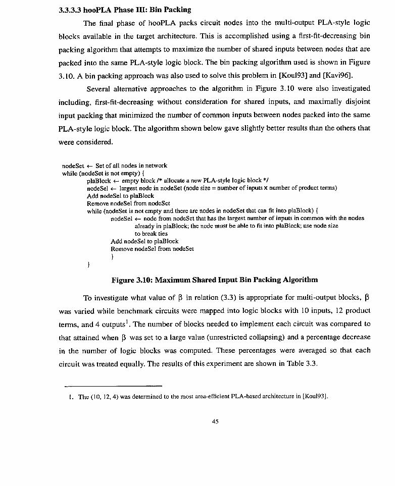
3.3.3.3 hooPLA Phase III: Bin Packing
The final phase of hooPLA packs circuit nodes into the multi-output PLA-style logic
blocks available in the target architecture. This is accomplished using a first-fit-decreasing bin
packing algorithm that attempts to maximize the number of shared inputs between nodes that are
packed into the sarne PLA-style logic block. The bin packing algorithm used is shown in Figure
3.10. A bin packing approach was also used to solve this problem in [Kou1931 and [Kavi96].
Several alternative approaches to the algorithm in Figure 3.10 were also investigated
including, first-fit-decreasing without consideration for shared inputs, and maximally disjoint
input packing that minimized the number of common inputs between nodes packed into the same
PLA-style logic block. The algorithm shown below gave slightly better results than the others that
were considered.
nodeset + Set of al1 nodes in network while (nodeset is not empty) {
plaBlock t empty block /* allocate a new PLA-style logic block */ nodeSe1 t largest node in nodeset (node size = number of inputs x number of product terms) Add nodeSe1 to plaBlock Remove nodeSe1 from nodeset while (nodeset is not empty and there are nodes in nodeset that can fit into plaBlock) {
nodeSe1 t node from nodeset that has the largest number of inputs in common with the nodes already in plaBlock; the node must be able to fit into plaBlock; use node size to break ties
Add nodeSe1 to plaBlock Remove nodesel from nodeset 1
1
Figure 3.10: Maximum Shared Input Bin Packing Algorithm
To investigate what value of p in relation (3.3) is appropriate for multi-output blocks,
was varied while benchmark circuits were mapped into logic blocks with 10 inputs, 12 product
terms, and 4 outputsl. The number of blocks needed to implement each circuit was cornpared to
that attained when p was set to a large value (unrestricted collapsing) and a percentage decrease
in the number of logic blocks was computed. These percentages were averaged so that each
circuit was treated equally. The results of this experiment are shown in Table 3.3.
1. The (1 0, 12,4) was determined to the most area-efficient PLA-based architecture in [Kou1931

Table 3.3: Effect of Controlled Partial Collapsing
Average % 1 1 Decrease 1
The results above suggest that it is not always a good idea to pack as much logic as
possible into each feasible node before packing the nodes into multi-output logic blocks. The
results also show that the number of outputs on the PLA-style blocks in the target architecture
should be taken into account when feasible nodes are generated by phases 1 and II of hooPLA.
One direction for future work wouId involve making modifications to phase 1 of hooPLA to take
this notion into account.
3.3.3.4 Cornparison with Existing Technology Mappers
To assess the quality of mapping solutions produced by hooPLA, the tool was compared
with the two technology mapping methods discussed in Chapter 2. In particular, hooPLA was
compared with the tool used by Kouloheris, called DDMAP [Kou193], and also compared with
the method of using the SIS [Sent921 partial collapsing function, eliminate', along with the node
partitioning and packing program called Break-a-Node, developed by ~ a v i a n i ~ [Kavi97]. Note
that the first step of DDMAP is to apply a look-up-table technology mapper; Level-Map [Farr94]
is used to perform this initial rnapping3.
Table 3.4 shows the results when the technology mappers are used to map benchmark
circuits into a target architecture containing unfoldable logic blocks with 10 input columns, 12
1. The partial collapsing routine in SIS is called eliminate. The routine was used in used in four diffcrcnt ways and the best solution was chosen: 'climinate -1 24 5'' 'eliminatc -1 24 2', 'climinatc -1 20 5'' and 'eliminate -1 20 2'. The SIS command 'simplify -1' was called after eliminate.
2. Break-a-Node is used in the CAD flow of the hybrid FPGA architecture [Kavi96]. 3. Kouloheris conducted his original experiments using the LUT mappcr Chortle-crf [Fran92][Kou193].

second lists the number of Iogic blocks needed to implement each circuit when hooPLA is used.
The third and fourth columns give the results for the eliminate method and DDMAP, respectively.
In these columns, a percentage is given in brackets which represents the amount of additional
logic blocks needed to implement each circuit in comparison with hooPLA. On average, when the
circuits are mapped using the eliminate method, they require 21 -5% more logic blocks than when
they are mapped with hooPLA. When circuits are mapped using DDMAP, they require 93.8%
more blocks on average than when hooPLA is used.
Notice that hooPLA perforrns poorly for the benchmark 'ex5p'. For this circuit, DDMAP
produces a solution with nearly 80% fewer blocks than hooPLA. ex5p is a purely combinational
circuit possessing 8 primary inputs, and 63 primary outputs. Since the number of inputs to the
circuit is less than the number of inputs to the logic blocks in the (10, 12,4) architecture, Level-
Map produces a mapping containing 63 nodes: one node for each primary output. Level-Map
produces such a mapping because it is able to deal effectively with reconvergent paths within
circuits. Furtherrnore, for this circuit, most of the nodes in the Level-Map solution happen to be
feasible nodes. Many of the nodes have common inputs, allowing several nodes to be packed into
each 4-output logic block. To verify that the exploitation of reconvergent paths was the reason for
the superior mapping, the circuit was mapped with the LUT-based technology mapper, Chortle-crf
[Fran92], which deals with reconvergence in only a limited way. Chortle-crf produced a mapping
containing 363 nodes which is significantly greater than the 63 nodes in the Level-Map solution.
Since hooPLA breaks up a circuit into fanout-free trees and finds a covering for each tree, it is not
able to exploit reconvergent paths effectively, and hence, produces an inferior solution for this
benchmark.
To verify that the results favouring hooPLA were not a side-effect of the (10, 12, 4)
architecture used for comparison, the circuits were also mapped into a (16, 8, 4) architecture and
compared with the eliminate method. In this case, the eliminate method produced solutions with
an average of 37.1 % more blocks than hooPLA.

Benchmark
a h 4
apex2
apex4
bigkey
C5315
clma
CPS dalu
des
3.3.4 PLA Folding
So far, hooPLA has been
been described as a technology
section reviews previous work on
ex5p ex1010
i 10
misex3
pair
pdc ~38417
described without any mention of PLA folding;
rnapper for normal unfoldable PLA-style logic
hooPLA
155
that is, it has
blocks. This
132
217
1 70
154
104
61 8
603
folding and describes the synthesis techniques used to perform
eliminate method (% more)
201 (29.7)
simple bipartite PLA folding. This is followed by a discussion of how PLA-folding is integrated
into the hooPLA algorithm.
DDMAP (% more)
199 (28.4)
335 (54.4)
196 (15.3)
190 (23.4)
116 (1 1.5)
700 (16.1)
s38584.1
seq spla
339 (54.8)
193 (0.0)
686 (202.2)
236 (1 56.5)
1458 (52.4)
159 (32.5)
102 (59.4)
456 (1 00.0)
219 1 278 (26.9)
193 160 (-17.1)
227 1 337 (48.5)
92 1 28 (39.1 )
957 1221 (27.6) l
27 (-79.5)
207 (4.6)
436 (156.5)
214 (39.0)
164 (57.7)
1221 (97.6)
1208 (100.3)
722 ( 13.2)
274 (19.7)
755 (27.3)
223 (37.7)
252 (1.2)
190 (46.2)
65 (32.7)
7 12 (35.9)
357 (-5.1)
253 (6.8)
151 (0.0)
164 (18.8)
352 (7.0)
Average: 21.5 %
63 8
229
593
120
64
228
977 (53.1)
337 (47.2)
1 160 (95.6)
3 12 (92.6)
1424 (47 1.9)
160 (23.1)
58 (1 8.4)
394 (-24.8)
173 1 (360.4)
9 1 1 (284.4)
301 (99.3)
368 (78.6)
275 (99.3)
536 (62.9)
Average: 93.8%
137 (14.2)
70 (9.4)
320 (40.4)
enc-shift-dec 1 162
fir
fsm8-16-13
fsm8-8-13
go164
mle
pmac
psdes
r4000-32
sort
valu
249
130
49
524
376
237
151
206
138
3 29

3.3.4.1 Previous Work
Egan and Liu showed that the problem of finding an optimal bipartite folding is NP-
complete [Egan84]. This implies that an algorithm with exponential time complexity must be
used to find a folding of optimal (maximum) size for a given PLA. The rnethod of branch and
bound was applied in [Egan84] to find optimal bipartite foldings. Several other heuristic methods
have been proposed.
Simulated annealing is a general algorithmic approach that was applied to the folding
problem by Wong, Leong, and Liu wong87-J. The authors developed a cost function, an
annealing schedule, and a simple method of moving from one solution to the next which consists
of permuting two rows of the PLA personality matrix. In this, and similar work [Sanc95], the
authors show how their algorithms can be adjusted to deal with specific constraints on the folding
problem such as bounded product terrn positions or ordered connection line assignment in which
a partial ordering is imposed on the PLA's input signals.
Another method undertaken in several studies is to translate the folding problem into a
graph partitioning problem and then apply heuristic min-cut partitioning [Lakh90][Liu94]. This is
the approach used in this thesis, and it is discussed in the next section.
Other approaches include mapping the folding problem into the problem of maximal
clique identification' in a graph [Leck89]; a simple greedy algorithm can be used to locate
cliques. Kuo, Chen, and Hu reformulate the folding problem as an integer programming problem
[Ku0851 [Pres95].
Hsu, Lin, Hsieh, and Chao consider the problem of combining Iogic minimization and
folding for PLAs [HsuQl]. The basic premise of the work is to examine how decisions made
during logic synthesis affect the amount of folding that can be achieved. The authors propose a
type of folding-directed logic synthesis that leads to increased folding sizes for some PLAs.
3.3.4.2 Approach Used to Perform Bipartite Folding
In this thesis, bipartite PLA folding is performed using an algorithm similar to the one
developed by Liu and Wei [Liu94]. Specifically, the algorithm in [Liu941 has been adapted to be
able to perform combined folding. The approach used involves mapping a PLA description into a
1. Maximal clique identification is the problem of finding the largest fully connected subgraph in a graph.

ulpai L l L G SiUylI UiiU L I l b l l UpYlJ L A I S L l l l l l - b U L S L U ~ l l Y U l L I L l V l 1 1 1 A 6 L W Y L V U U b b U L W l U 1 1 1 6 . A W L Y U I L I L b
graph is an undirected graph, G = (V, E) , in which V can be divided into two sets, VI and V2,
such that each edge, (u, v ) cz E , indicates that u E V1 and v E V2 [Corm94]. Thus, al1 of the
edges in a bipartite graph connect vertices in the different vertex sets, V I and V2.
A PLA can be transformed into a bipartite graph by letting each vertex in the first vertex
set, VI , correspond to a single product term of the PLA and each vertex in the second vertex set,
VZ , correspond to one of the PLA inputs or outputs. An edge exists between a node u E V I and a
second node v E V2 if one of the following two conditions are true:
1. v is an input, and it is used in the product term represented by u . 2. v is an output, and the product term represented by u is a terrn in the sum-of-products
function that v irnplements.
The transformation of a PLA into a bipartite graph is shown in Figure 3.1 1.
Figure 3.11: Mapping a PLA into a Bipartite Graph
Following the transformation of the PLA into a bipartite graph, the newly created graph,
G , is partitioned into two subgraphs, G, and G 2 . A min-cut algorithm similar to that developed

between nodes in the two different subgraphs. The following parameters can be deterrnined for
any partition, P , of G :
X I = {xlx E V2, x adjacent to vertices in G1 only, x represents an input} (3.4)
X1 = { X ~ X E V2, x adjacent to vertices in G2 only, x represents an input} (3.5)
X 3 = { X lx E VI, x adjacent to vertices in G , only } (3.6) X4 = {X lx E V I , x adjacent to vertices in G2 only ) (3.7)
Once these vertex sets have been identified, the size of the column folding corresponding to P is
Similarly, the size of the row folding corresponding to P is given by:
R = min(lx31, Ix41 Only inputs are included in the sets X I and X2, since outputs are not allowed to be folded'. A
graphical interpretation of the concepts above and a partitioned version of the bipartite graph of
Figure 3.11 is shown in Figure 3.12. In the figure, a single edge crosses between the subgraphs
G, and G 2 . The value of C and R are 2 and 1, respectively. The folded PLAs corresponding to
the partitioning are displayed beneath the partitioned graph.
- . . -. .. - . -
1 . Outputs are not allowed to be folded because of the register and drive circuitry associated with each output.
5 1

Figure 3.12: Partitioned Bipartite Graph with Foldings
The partitioning algorithm works as follows: First, the vertices of the bipartite graph are
randomly partitioned into two subgraphs, G , and G 2 , and al1 vertices as tagged as 'free',
meaning they are free to move between subgraphs. Next, the free vertex with the highestfimess
(defined shortly) is selected and moved to the opposite subgraph. The selected vertex is then
tagged as 'locked' meaning that it may no longer move between subgraphs. After each move,
equations (3.8) or (3.9) above are used to determine if the current partitioning is the best found so
far; (3.8) is used for column folding, (3.9) for row folding. The best partitioning is saved. This
process of selecting, moving, and locking continues until there are no more free vertices,
indicating that the 'pass' is compIete.
A second pass is initiated by freeing al1 vertices and setting the initial partition equal to the
best partition found during the previous pass. These partitioning passes continue until there is a

complete.
When coIumn folding is being performed, the fitness of moving a vertex, v, to the
opposite subgraph is computed using:
Fitness(v) = v is rnoved - Cbefore v iç moved (3.10)
When row fo1ding is being performed, the fitness of a moving v is computed using:
Fitness(v) = i~ is rnoved - Rbefore v is rnoved (3.1 1)
Pseudo-code for the folding aIgorithm is given in Figure 3.13.
Fold (G)( /* G is the bipartite graph representation of a PLA */ BestP t random partition of the vertices in G modified t true while (modified) { /* begin a pass */
free al1 vertices in G set the initial partition equal to BesrP modified t faIse whi1e there are free vertices (
select the vertex with the highest fitness move the selected vertex to the opposite subgraph and Iock it if the size folding corresponding to the current partition >
the size of the folding corresponding to BestP ( BestP t the current partition modified t true 1
1
Figure 3.13: Pseudo-Code for Folding Algorithm
One significant feature of this folding algorithm is that either row or column folding can
be performing using the same bipartite graph and partitioning algorithm. Combined folding is
achieved by first performing either row or column foiding. This primary folding is tantamount to
dividing the original PLA into two smaller PLAs. Subsequent folding can then be applied to these
smaller PLAs by transforming them into bipartite graphs and applying the same folding
algorithm. The division of a folded PLA into two smaller PLAs is shown in Figure 3.14.

a b c 'f Z
Figure 3.14: Division of a Folded PLA into Two Smaller PLAs for Subsequent Folding
One problem that arises in the subsequent folding of the two smaller PLAs is related to the
fact that there may be inputs (or product terms) that are present in both of the smaller PLAs. This
is true for the case of the small PLAs in Figure 3.14 which share the product terrns P4 and P5.
This sharing leads to a situation in which folding one of the smaller PLAs may introduce
constraints on the folding of the second smaller PLA. Column folding can be thought of as a
partial ordering of a PLA's product terms - some product terms above the breaks, and some
product terms below the breaks. Similarly, row folding can be thought of as a partial ordering of a
PLA's inputs and outputs - some of the inputs and outputs to the left of the breaks, some of the
inputs and outputs to the right of the breaks. To understand how the constraints are created,
consider the following example. A large PLA with two outputs is row folded and thus divided into
two smaller PLAs. Assume that the two smaller PLAs have two product terms in common and
that subsequent column folding on the first small PLA results in a partial product term ordering in
which both of the common product terms are located above the breaks. This introduces a
constraint on the column folding of the second small PLA: both of the common product terms are
constrained to be above the breaks in the folded PLA'. The reason for the constraint is that
1 . Equivalently, both of the product tenns may be constrained to be below the breaks in the folded PLA. The constraint is simply that the nodes representing the two shared product terms be in the same partition after the bipartite graph partitioning step.

eventually be re-assembled into a single combined folded PLA. These additional constraints can
be realized within the context of the folding algorithm described above by allowing vertices to be
pre-allocated to one of the subgraphs, G , or G 2 , and by allowing a permanent lock to be placed
on some vertices of the bipartite graph. Perrnanently locked vertices are never allowed to move
between subgraphs.
3.3.4.3 Integrating PLA Folding into hooPLA
In essence, the goal is to use folding to pack additional logic into each logic block. The
folding algorithm described in the previous section was applied in several different ways. The first
attempt involved trying to maximize the sum of the sizes of the nodes that are packed into a single
foldable PLA-style logic block. That is, attempting to maximize BlockSize in the following
equation:
BlockSize = size(u) U E B
where B is the set of nodes that are packed into a multi-output PLA-style logic block. Folding
was integrated into phase III of hooPLA and nodes were selected to be packed into foldable PLA-
style blocks on the basis of their size. The largest node that could fit into the PLA-style block
being considered was selected and packed, even if folding was necessary to make the node fit into
the multi-output block.
The second method investigated was simpler and gave slightly better results. This method
attempts to maximally utilize al1 of the outputs on logic blocks. In this approach, phase III of
hooPLA is perfonned as it would be for an architecture with unfoldable blocks (as described in
Section 3.3.3.3). This inevitably leads to PLA-style blocks with unused outputs. Folding is then
applied to identify additional nodes that can be packed into the multi-output blocks until al1
outputs are utilized. Given a situation where several nodes are identified as candidates to pack into
a logic block, the node with the most inputs in common with nodes already in the logic block is
selected and packed.
Phase II of hooPLA was designed for unfoldable logic blocks and it attempts to eliminate
nodes from a circuit by collapsing them into their successors. As described previously, when
mapping into an architecture with the parameters (1, P, O), a node is not collapsed into its

- - -
P product terms. Phase II was modified and incorporated with column folding to allow more
nodes to be collapsed into their fanouts and eliminated from the network. In the modified version,
a node can be coIlapsed into its successors as long as the nodes that result from collapsing have
less than or equal to P product terms, and less than or equal to F inputs. F may be Iarger than I as
long as a colurnn folding can be found such that F minus the size of the folding is less than or
equal to 1. Clearly, this modification of hooPLA is only appropriate when the target architecture
has either column or combined foldable logic blocks. It gives good results for some circuits, and
therefore, the folding results presented in the empirical study in Chapter 5 reflect the best folding
results achieved both with or without using this modification.
One folding method that was not attempted is to combine folding into phase 1 of hooPLA.
Currently, hooPLA covers fanout-free trees with feasible nodes where each feasible node can fit
into a normal unfolded PLA-style block. Phase 1 of hooPLA could be modified to cover fanout-
free trees with nodes that possess more inputs than that which could fit into a normal unfolded
PLA-style block, but that could be folded to fit into a column or combined foldable PLA-style
logic block. This would increase the size of the search space in the optimal tree mapping and it
would make hooPLA significantly more complex, but it may give superior results.
3.4 Summary
In this chapter the foldable PLA-style logic block architecture was introduced.
Implementing foldable PLA-style logic blocks is feasible in LPGA technology since it is possible
to cut metal Iines. The proposed logic block architecture represents an entirely new application for
PLA folding which has previously only been used in custom VLSI. A brief review of PLA folding
was given along with the rationale for choosing to use simple bipartite folding.
A CAD flow to rnap circuits into the proposed architecture was presented. The CAD flow
includes a new tooI, called hooPLA, that was designed and implernented to perform technology
mapping for architectures with foldable PLA-style blocks. The hooPLA algorithm operates in
three phases. Phase 1 uses dynamic programming to map each fanout-free tree in a circuit's DAG
into a new tree possessing the minimum number of feasible nodes. Phase II attempts to eliminate
nodes by collapsing them into their successors. Phase III is a bin packing step in which the nodes
in a circuit are packed into multi-output logic blocks. Folding was achieved using a min-cut graph

algorithmic flow of hooPLA is summarized in Figure 3.15.
Break circuit's DAG into a forest of fanout-free trees.
Phase 1: Map each tree into a new tree
possessing the minimum number of feasi ble nodes.
Re-assemble circuit from trees and collapse nodes across tree boundaries. Optionally, perform
folding when target is column or combined foldable logic blocks.
Phase III: Pack nodes into PLA-style logic blocks.
Use folding to pack as much logic as possible into each logic block.
Circuit mapped into foldable PLA-style logic blocks.
Figure 3.15: Algorithmic Flow of hooPLA

4.1 Introduction
This chapter introduces the foldable look-up-table logic block architecture. Section 4.2
shows how the proposed architecture is related to LUT-based FPGAs and outlines its relevant
architectural parameters. Synthesis techniques for mapping circuits into foldable LUTs are
presented in Section 4.3. A custom CAD tool has been developed, and it is used in conjuction
with an existing FPGA CAD tool to realize a CAD flow for targeting foldable LUT-based
architectures.
4.2 Foldable Look-Up-Table-Based Logic Block Architecture
Chapter 2 introduced LUT-based logic blocks and reviewed several important research
results and synthesis techniques. A LUT is a multiplexer tree and a set of storage elementsl. LUTs
have an area-efficient implementation in LPGA technology. Instead of using SRAM cells for the
LUT's storage elements, each storage element is implemented as a programmable connection to
either logic 'O' or ' l ' , as shown in Figure 4.1. The LUT's "storage elements" require no
transistors. During laser programming, either the connection to logic '1', or the connection to
logic 'O' is cut away according to the tnith table of the logic function being implemented in the
LUT. This causes the programmed LUT to resemble a small ROM. A similar LUT
implernentation can be found in the Xilinx XC3300 mask-programmed gate array2. The XC3300
has the same architecture as the SRAM-based XC3000 FPGA, but, in the XC3300, SRAM cells
are replaced by 'programmable vias', resulting in a die size 50% smaller than an equivalent
SRAM-based part [Frak92].
1. An example of a 4-LUT is depicted in Figure 2.7. 2. The XC3300 is an MPGA with two fully-customizeable metal layers.

Select Lines
Figure 4.1: LUT Programming in LPGA Technology
K There are 2 storage elements in a K-LUT; the number of 2 to 1 multiplexers in a K-
LUT is 2K - 1 . These structures dorninate the silicon area consurned by a LUT [Rose90], rnaking
the area of a LUT exponentially related to the parameter K. Therefore, to achieve good area-
efficiency, it is critical to utilize LUT inputs effectively. When a 4-LUT is used to implement a
function of only 3 inputs, half of its logic capacity is wasted. Current technology mappers for
LUTs do a reasonable job of utilizing LUT inputs when K is small; however, as K is increased, a
signifiant number of inputs are left unused. This effect can be seen in Figure 4.2 which shows the
average number of LUT inputs that were left unused when the Level-Map technology mapper
[Farr94] was applied to the 30 benchmark circuits listed in Appendix A. Although increasing the
number of inputs to LUTs in the target architecture reduces the number of LUTs needed to
implement circuits, the reduction must be traded-off with the increase in logic block and routing
Number of LUT Inputs (K)
Figure 4.2: Utilization of LUT Inputs

the abiIity to cut metal lines. A 4-input LUT contains two 3-input LUTs within it. Through the
addition of cut points, extra inputs, and outputs, a LUT could optionally be divided in half. Figure
4.3 shows a 4-input LUT with added cut points so that it may be divided into two 3-LUTs. The
multiplexers that implement each of the 3-LUTs are shown with different shading. The term
folding refers to the division of a LUT into smaller LUTs. LUT folding is tantamount to varying
the granularity of the logic blocks in the target architecture. The capability to divide LUTs in this
way increases the amount of 1ogic that may be packed into a single LUT. For example, consider
the case of mapping a circuit into an architecture with 4-LUTs. If the logic blocks are not
foldable, a logic block is needed to implement each 3-input node in the circuit. However, if
folding is permitted, two 3-input nodes can be paired together and irnplemented in a single logic
block. The notion of foldable LUTs is similar to the notion of 'decomposable look-up-tables' in
Input 4 Input 5 Input 6 I
1; t E H
01 Li
2 : i îü u = "Stomge Elernent" ? n = Laser Cut Point w
Input O Input 1 Input 2 Input 3
Figure 4.3: Foldable 4-LUT
This ability to divide LUTs can be extended. For instance, a 4-LUT can implement one 4-
LUT, two 3-LUTs, five 2-LUTs, and some combinations of 3-LUTs and 2-LUTs. The laser cut-
points necessary to achieve this fiexibility are shown in Figure 4.4. The multiplexers that
implement each of the five different 2-LUTs in a 4-LUT are shown with different shading. As
iIlustrated in the figures, there is some overhead involved in being able to fold LUTs.
Implementing two 3-LUTs in a single 4-LUT means that the logic block must have two outputs.

The multiplexer outputs in Figure 4.4 are labelled "potential" outputs because although 7 outputs
are shown, a maximum of 5 different logic functions can be implemented in the logic block;
therefore, five output drivers would be needed. Furthemore, folding increases the number of
inputs to each logic block. Each input must be present in its tnie and complemented forrn for the
multiplexer select lines. Thus, inverters are needed for each of the additional logic block inputs.
Lastly, folding may increase the number of "storage eiements" in a LUT as shown in Figure 4.4,
in which four new storage elements were introduced.
An architecture with foldable LUTs can be characterized by two parameters, K and L.
The parameter, K, is equal to the number of inputs to the LUT in its unfolded forrn. The
parameter, L , is referred to as the foldingflexibility, and it is equal to the nurnber of inputs to the
smallest LUT into which the original LUT may be divided. For exarnple, the foldable LUT shown
in Figure 4.4 has the parameters K = 4 and L = 2, since it can be divided into 2-LUTs.
Normally, in LUT-based FPGAs, each logic block contains a register [Alte96][XiIi94].
Clearly, it is not feasible to have a register associated with each output of a foldable LUT, because
it would greatly increase logic block area. In this study, it is assurned that each logic block has a
single register that can optionally be bypassed to implement combinational logic. The register
bypass can be implemented in LPGA technology in a way that requires no multiplexers. It is
further assumed that any of the potential outputs of the combinational portion of a logic block
may connect to the register input. The output circuitry for a foldable LUT-based logic block with
K = 4 and L = 3 is shown in Figure 4.5

Input 4 Input 5 Input 6
I I I I
Input O Input 1 Input 2 Input 3
Figure 4.4: Foldable 4-LUT with Additional Flexibility
"Stonge Element" Laser Cut Point
Potential Output FromRoot - Multiplexer of Multiplexer Tree
Actual Outputs
I I I - -\ Output Dnvers Potentid Outputs Laser Cut Point
Figure 4.5: Output Circuitry for Foldable LUT-Based Logic Block with Parameters K = 4 and L = 3
As folding flexibility is increased, the number of logic blocks needed to implement
circuits should decrease because more logic can be packed into each LUT. This decrease must be
traded-off with the area penalties connected with the added flexibility. The empirical study in
Chapter 5 is concerned with whether or not there is an optimal amount of folding flexibility for
LUT-based logic blocks.
4.3 Synthesis
This section discusses a CAD flow for foldable LUT-based architectures. A high-level
overview of the flow is given in Section 4.3.1. Following this, Section 4.3.2 introduces a new tool
that has been developed to perfonn technology rnapping for foldable LUT-based logic blocks.

4.3.1 Overview of CAD Flow
The CAD flow for foldable look-up-table-based logic blocks is shown in Figure 4.6. The
front end of the flow is identical to the front end of the CAD flow for foldable PLA-style logic
blocks discussed in Chapter 3. The issues related to technology independent synthesis that were
presented in Chapter 3 apply equally well to synthesis for foldable LUTs, and they will not be
repeated here. Circuits are mapped into the gates of a 4-bounded intermediate target library using
Synopsys tools [Syn96]. The library consists of elements from Altera's FLEX 8000 FPGA library
[Al te951.
Behavioural HDL Circuit State Machine MCNC Circuit (edif netlist) or RTL, HDL Circuit
\
\
\ RTL WDL
\ Circuit
Library of Synopsys Design Compiler 4-Bounded
/ Verilog Netlist
Using ver2blif
Netlist of
Trmsferred to BLIF
Level-Map
Unfolded
Nctlist of Folded Look-Up-Tables
Figure 4.6: CAD Flow for Mapping Circuits into Foldable LUT-Based Logic Blocks
Synthesis proceeds in a manner typical for LUT-based FPGAs. The Level-Map [Fan941
technology mapper is used to map circuits into a network of normal unfolded LUTs. Level-Map
was discussed in Chapter 2.
After technology mapping with Level-Map, some circuit nodes may not use al1 of their K

into a single foldable LUT. A tool, called LUTPack, has been developed and integrated into SIS
[Sent921 to perforrn this packing.
4.3.2 LUTPack: Technology Mapping for FoIdable Look-Up-TabIe-Based Logic Blocks
A LUT contains a binary tree of multiplexers. Large LUTs can be decomposed into
smaller LUTs by cutting the multiplexer tree into smaller trees. Circuit nodes with less than K
inputs are referred to as small nodes. LUTPack uses a first-fit-decreasing (FFD) approach to pack
multiple small nodes into a single foldable LUT-based logic block. In essence, the algorithm must
'cover' the multiplexer trees in the logic blocks with small nodes that exist after technology
mapping. LUTPack attempts to minimize the total number of logic blocks needed to implement a
circuit.
First-fit-decreasing bin packing algorithms are commonly ernployed for problems in
which a number of elements must be 'packed' into bins tbat have a fixed capacity. The reason this
type of algorithm cannot be applied directly to the problem of packing small nodes into LUTs is
that FFD algorithms consider only the size of the elements and the bin capacity. To perform
technology mapping for foldable look-up-tables, it is also necessary to consider the location of
the elements within a bin. That is, it is necessary to consider how the
blocks are covered with small nodes.
To illustrate the algorithm, it is important to consider what
small nodes with L inputs that can be packed into a LUT with K
found using equation 4.1.
multiplexer trees in the logic
is the maximum number of
inputs. This number can be
LLJ
Number of L-LUTs = 2K - jL = i = 1
where L I K
The maximum described in (4.1) can be achieved only if the smaller nodes with L inputs
are packed into the K-LUT in a 'bottom-up' manner; that is, from the leaf multiplexers of the K -
LUT'S multiplexer tree towards the root multiplexer. For example, consider the problem of
packing two 3-input nodes into a 4-LUT. This is illustrated in Figure 4.7 where the multiplexers
are shown as nodes in a binary tree. To keep the figure simple, inputs to the LUT are not shown.

node covers the portion of the multiplexer tree closest to the root multiplexer (the covered portion
of the tree is shaded). This placement precludes the possibility of packing any additional 3-input
nodes into the 4-LUT. Part (b) of the figure shows how it is possible to pack two 3-input nodes
into the 4-LUT, if they are in locations closest to the leaf multiplexers. To achieve the best
utilization of the multiplexers in LUT-based logic blocks, it is best to cover the multiplexer trees
in a bottom-up fashion. Parameter L may be chosen such that there exists circuit nodes with less
than L inputs. During packing (covering), these nodes will consume a portion of the tree equal to
that consurned by a node with exactly L inputs.
Root Multiplexers I
I I I I I I I I I I
(a) Poor Covering LeafMultiGexers (b) G O O ~ Covering
Figure 4.7: Covering the Multiplexer Wee
One additional objective of the algorithm is to attempt to limit the number of distinct
inputs to a single logic block. The reason for this is that the number of connected input pins per
logic block is directly proportional to the average number of routing tracks required to route
circuits [ElGa8 11. Consequently, this secondary objective rnay help improve routability, given that
the number of tracks available is fixed.
Some circuit nodes are registered, and, as stated earlier, it is assumed that there is a
maximum of one register per logic block. Two algorithms were investigated to deal with this. The
first algorithm did not confer any special preference on registered nodes when choosing nodes to
pack into a block. In this algorithm, nodes were selected on the basis of their size' and the number
of inputs shared with nodes already packed into a block. The second algorithm attached special
1. In this case, size is equaI to the number of inputs to a node.

packing. In the case of the second algorithm, node size and minimizing the number of distinct
inputs to a logic block were secondary selection criteria. These two algorithms were compared in
a study in which benchmark circuits1 were mapped into foldable LUTs with the parameters K = 6
and L = 4. The number of foldable blocks needed to irnplement each circuit was determined and
compared with the number of logic blocks needed when the circuit was mapped into an
unfoldable architecture with K = 6. A percentage reduction in number of logic blocks was
computed for each circuit, and these percentages were averaged over al1 circuits. The second
algorithm never performed worse than the first algorithm, and it produced better results for a few
circuits; hence, it was chosen as the packing technique. Figure 4.8 provides pseudo-code for the
algorithm used to cover the multiplexer trees.
LUTPack { IutSet c- Set of aIl nodes in network while (lutset is not empty) {
donepacking e false FoldableBlock e empty block /* allocate a new logic block */ LUT + largest registered node in lutset; if there are no registered nodes in lutset, select
the largest unregistered node Remove LUT from lutset Add LUT to FoIdableBlock in a position as close as possible to the leaf
multiplexers of FoldableBlock while (donepackhg is equal to false and lutset is not ernpty) (
LUT t largest unregistered node in IutSet that can fit into FoldableBlock - use the number of shared inputs to break ties
If LUT exists { Remove LUT from lutset Add LUT to FoldableBlock in a position as close as
possible to the leaf multiplexers of FoldableBlock 1
else ( donePacking c tme 1
1 1
1
Figure 4.8: Pseudo-Code for First-Fit-Decreasing LUT Packing
1 . The benchmark circuits used in the study are those Iisted in Appendix A.
66

This chapter introduced the foIdable look-up-table logic block architecture. The proposed
logic block is characterized by the parameters K and L. K represents the number of inputs to the
logic block in its unfolded form. L is referred to as the folding flexibiIity, and it is equal to the
number of inputs to the smallest LUT into which the larger K-LUT may be divided.
A tool named LUTPack has been developed to cover the binary tree of multiplexers in a
K-LUT with small nodes having less than K inputs. LUTPack uses a first-fit-decreasing approach
and covers multiplexer trees in a bottom-up fashion.

-
5.1 Introduction and Architectural Questions
In this chapter, the synthesis techniques described in Chapters 3 and 4 are applied to
investigate the advantages of foldable PLA-style logic blocks and foldable look-up-table-based
logic blocks. Some of the architectural questions addressed are:
Can the number of logic blocks needed to implement circuits be reduced if logic blocks
are foldable?
What are the advantages of row folding, column folding, and combined folding in
PLA-styie logic blocks? What are the effects of allowing folding in look-up-tables?
Assuming that folding can reduce the number of logic blocks needed to implement
circuits, can it actually reduce silicon area, when both routing and logic area
are taken into account?
Would an LPGA architecture based on the proposed coarse-grained foldable blocks
exhibit superior predictability than the finer-grained state-of-the-art CX200 1 LPGA?
5.2 Experimental Procedure
An empirical approach is used to study the foldable architectures. Experiments consist of
mapping a set of benchmark circuits into the experimental architectures. Architectural parameters
are varied to study the effect they have on the mapping solutions. For the foldable PLA-style
blocks, the number of inputs columns (0, product term rows (P), and outputs (0) are varied, and
the effects of row folding, column folding, and combined folding are investigated. For the
foldable look-up-table logic blocks, the number of inputs to the LUT in its unfolded form (K ) , and
the folding flexibility (L), are varied.
5.2.1 Benchmark Circuits
A set of 30 benchmark circuits from three sources are used in this study. The benchmarks,
their sources, and their sizesl are listed in Appendix A. A total of 19 of the circuits are large
1. The size of each benchmark is given in terms of unfolded 4-LUTs and unfolded (10, 12,4) PLA-style logic blocks.

in Appendix D. The last circuit is a processor benchmark from the PREP synthesis suite
[PREP96].
5.2.2 Area Models
To determine the relative area-efficiencies of the foldable architectures, area rnodels are
used. The models assume that silicon area is consumed by a combination of logic and routing,
with the possibility that some routing may be placed in metalization layers directly on top of
active logic. This is different than the area mode1 that has traditionally been used in FPGA
architecture research [Rose90], where the area consumed by routing is assumed to be separate
from active logic area. Routing on top of active logic is feasible in LPGA technology because the
routing circuitry present in LPGAs is entirely metal, and it contains none of the SRAM bits, pass
transistors, or anti-fuses [Brow92] that are used to create programmable routing connections in
FPGAs.
Since the amount of routing resources that may be placed on top of active logic is limited
by the area of each logic block and the laser cut points needed to configure the logic circuitry, two
area modeIs are used: one pessimistic, the other optimistic. These two models are depicted in
Figure 5.1. The pessimistic model assumes that only vertical routing tracks may be pIaced on top
of active logic. Depending on the number of vertical routing tracks, the logic blocks may either be
abutted, or some space may exist between adjacent blocks. The optimistic model assumes that it is
possible for both horizontal and vertical routing resources to be located on top of logic. These two
area models serve as upper and lower bounds for the area that will be needed for each
experimental architecture. The exact area needed can be determined only through the detailed
VLSI layout of logic blocks and routing resources.
A basic tile is defined to be the area of a single logic block and its adjacent routing
circuitry. The basic tile structure is shown in Figure 5.1. Using the pessimistic area model, the
area of a basic tile is:
TileAreapcss = height x width = (m + W - R,,) x r n a x ( m , W . R,) (6.1)
where W is the number of tracks in a routing channel, R , is the routing pitch, and LA is the area
of a logic block. For simplicity, logic blocks are assumed to be square. The max function reflects

is applied, then the area of a basic tile is:
TileArea,,,, = rnax(LA, (W R p ) 2 )
The total area needed to implement a circuit is equal to the number of logic blocks needed
multiplied by the tile area. The models assume that there are equal arnounts of horizontal and
vertical routing resources. An empirical study by Betz showed that this routing architecture leads
to the smallest possible routing resource area in FPGAs [Betz96].
Basic Tile (Pessimistic Model)
Optimistic Model
Basic Tile (Optimistic Model)
Pessimistic Model
Figure 5.1: Pessimistic and Optimistic Area Models
Both routing and logic area are measured in terms of the technoIogy independent
parameter h [Mead80], which is equal to half the minimum feature size in a given technology. In
a typical LPGA technology, accounting for the overhead needed for laser cut points, R , is
approximately equal to 1 1 A.
5.2.3 Chip Area of Foldable PLA-Style Logic Blocks
A chip area mode1 for foldable PLA-style logic blocks was developed using a layout
autornatically generated by the PLA layout generation program MPLA' [Scot85]. The generated
layout is given in Appendix C; its floorplan is shown in Figure 5.2. The PLA layout is for a
1 . MPLA was developed at the University of California, at Berkeley.

models in this section were produced using the generated MPLA layout, and by estimating how
the layout would need to be modified so that it could be configured using the laser disconnect
methodology.
Clocked Pull-Up Transistors
Figure 5.2: PLA Layout Floorplan
The area of an unfoldable PLA-style logic block is estimated as:
LA = (24 .1+ 1 9 . 0 + 5 8 ) - ( 1 6 . P + 4 4 ) + lOOO.Z+l35OO.O+lOOO h2 (6.3)
where 1, P, and O represent the number of input columns, product term rows, and outputs of the
logic block, respectively. The first term in (6.3), (24 I + 19 O + 58), is the combined width of
the PLA's AND and OR-planes. The next term, (16 . P + 44), is the height of the PLA's AND-
plane. The 1000- I term accounts for the area consumed by the input buffers. The 13500 . O
term includes the area consumed by the latch' (-3500 h2) , flip-Rop (-8000 h2
[Vran97][Rose90]), and output driver (-2000 A') that are present for each logic block output.
The final constant, 1000, represents the area needed to buffer and invert the signal used to clock
the pull-up transistors in the AND and OR-planes. Row foldable PLAs have an OR-AND-01Z2
structure and thus, require pull-up transistors on both sides of the AND-plane. The logic area of a
row foldable logic block is estimated as:
LA =(24~1+19~0+84)~(16~P+44)+1000-I+13500~0+1000 h2 (6.4)
Column folded PLAs have extra inputs, and therefore, require additional input buffers. The logic
area of a column foldable PLA-style logic block is estimated as:
1 . The latch is needed for the PLA-style block to have zero stand-by power [Wong86]. 2. The OR-AND-OR structure of row foldable PLA-style Iogic bIocks is shown in Figure 3.5.

Low power is an important consideration in many LPGA applications. Low-power PLAs
can be built using the circuit techniques described in [Wong86] and [Frak89]. These PLAs
achieve zero stand-by power through the use of input transition detection circuitry, CMOS
dynamic logic, and sense amplifiersl. The PLA that was used to generate the models above is very
similar to the zero stand-by power PLA described in [Wong86], with the main difference being
that it contains no input transition detection circuitry. However, this circuitry is relatively small in
cornparison with the other circuit structures interna1 to the PLA. The PLA design in Wong861 is
used in a commercial CPLD architecture.
5.2.4 Chip Area of Foldable Look-Up-Table-Based Logic Blocks
As mentioned in Chapter 4, when LUTs are implemented in LPGAs, they require none of
the SRAM cells that dominate the area of LUT implementations in FPGAs. The chip area of a
foldable look-up-table-based logic block is estimated as:
where I is the number of inputs to the logic block (inputs are assumed to be buffered), N4, is
the number of 4 to 1 multiplexers contained within the LUT3 multiplexer tree, O is the number
of output drivers needed for the logic block, and 8000 [Vran97][Rose90] is the area consumed by
the flip-flop present in each logic block. Note that foldable LUTs will have larger values of I and
O than unfoldable LUTs with the same K. The area consumed by an output driver is
approxirnately 2000 h2. The area consurned by a 4 to 1 rnultiplexer without input buffers is
approximately 1000 h2. The number of 4 to 1 rnultiplexers in a K-LUT rnay be computed using
equation (4.1) in Chapter 4. To estimate the area of LUTs that do not contain an integral number
of 4 to 1 multiplexers, N4 1o , is not required to be an integer2.
1. Input transition detection circuitry is used dong with CMOS dynarnic logic to ensure that power is only dissipated when input transitions occur. In addition to this, dynamic power dissipation is reduced and speed is increased by using sense amplifiers on product term lines to eliminate the necessity for wide volt- age swings.
2. LUTs do not contain an integral number of 4 to 1 multiplexers when parametcr K is odd.

In this study, several important theoretical results are used to predict routing resource area.
In [EIGa81], El Gamal showed that the average number of used tracks in any channel of a gate
array with equal amounts of horizontal and vertical routing resources is given by:
where hpins is the average number of connected input pins per logic block for circuits
implemented in the gate array, and R is the average Manhattan length of two-point routing
connections (measured in the number of blocks)'. The parameter hpins in the above equation is
known after technology mapping is complete; however, placement and routing must be completed
if R is to be known exactly. In this study, routing resource area is estimated using equation (6.8)
above, and the value that results from performing placement and global routing for each circuit
in each architecture in its unfolded forrn. Placement and global routing is done using the CAD
system, VPR [BetzgBa]. During placement and routing, it is assumed that the clock, set, and reset
signals feeding the flip-flops in each logic block are routed on dedicated tracks, and that the pins
on logic blocks are distributed, with some pins being accessible to horizontal routing resources,
and some being accessible to vertical routing resources.
It is assumed that the maximum number of used tracks in any routing channel, W, is
greater than the average number of used tracks, W,,, . When each circuit is placed and routed in
an unfoldable architecture, the ratio of W to W,,, can be computed. This ratio is then used to
compute the number of tracks, W, needed to route the circuit in a foldable architecture; the ratio
is used by multiplying it by the value of WaV, that is computed using equation (6.8) after the
circuit is mapped into the foldable architecture. Table 5.1 shows the average ratios of W to W,,,
and average values of R for several unfoldable architectures. The numbers in the table were
computed by averaging across al1 30 benchmark circuits.
1 . In addition to (6.8), El Gamal determined that the number of tracks per channel follows a Poisson distribution. This assertion was verified by Brown in [Brow92a].

Table 5.1: Average Wire Length and Average Ratios of Maximum to Average Channel Density
I -
Unfoldable Architecture 1 Average R 1 Average W/Wavg I
The routing mode1 used in this study errs on the side of pessimism since work by Donath
and Feuer suggests that R will likely decrease as blocks are folded [Dona791 [Dona8 11 [Feue82].
In this previous work, it was shown that the average connection length in a region of C nodes
when placed on a square array is: 1
P - 5 R oc c
where p is the so-called 'Rent exponent9,' which, although it depends on the circuit being routed,
is typically about 213 Feue821. (6.9) suggests that will decrease as the number of blocks
needed to implement circuits decreases (given that p does not increase). Circuits implemented in
an architecture with large foldable blocks will need fewer blocks than when they are implemented
in architectures with smaller, or unfoldable blocks. This should lead to a decrease in R . Table 5.1
verifies that decreases as logic block granularity increases.
5.2.6 Limitations of Area Mode1
To more precisely compute the chip area needed for routing resources in the foldable
architectures, a new routing CAD tool would be needed. This is because the number of physically
different pins on each logic block varies when folding is used. This notion does not exist for logic
blocks that are not foldable. For instance, consider a column foldable PLA-style logic block that
1. The Rent Relationship [Dona79]. 1 = A cP . relates the number of external terminals, 1 , frorn a group of gates to the number of gates in the group, C, the average number of terminals per gate, A , and the Rent exponent, p. The value of p was originally taken to be 213 [Feue82].

L I U 3 l l l Y U L y 1 1 1 3 l b U U 1 1 1 6 3 1 6 1 1 U 1 3 U L U U L l l L l l b L V t f U I L U L 1 1 b U W L C V l l l U1 1 L J A A I Y tflU1lU. UUIllU b V l U 1 1 1 1 1 3 1 1 1
the logic biock may be folded, meaning that they contain a break. Two signals are fed to a folded
column, as the break in the column makes the signal at the top of the column physically different
than the signal at the bottom of the column. However, only a single signal is fed to an unfolded
column, and therefore, the signal may enter the logic block from either of two pins, making the
two pins that feed an unfolded column physically equivalent. To make efficient use of the blocks,
a router would need to understand how Iogic block pins can best be used. A new routing CAD tooI
has not been developed for this study; however, it is believed that the area model being used is
sufficiently accurate, and the effort needed to develop a new routing tool is not merited.
5.3 Area-Efficiency Results for Foldable PLA-style Logic Blocks
In this section, the benefits of folding in PLA-style logic blocks are explored. The
advantages of row, column, and combined folding are studied for architectures containing PLA-
style blocks of various sizes, ranging from 8 input columns, 8 product terrn rows, and 3 outputs to
24 input columns, 24 product terrn rows, and 5 outputs. The results are presented in two ways: 1)
as a reduction in the number of blocks needed to implement circuits, and 2) an area is presented
for each experimental architecture; the area is computed using the area models described in the
previous section. Only the results obtained by applying the optimistic area model are included in
this chapter; the results obtained by applying the pessimistic model are included in Appendix B.
When numerical data results are quoted in the text of this chapter, the data result corresponding to
the pessirnistic area model wilI be given in parentheses.
5.3.1 The Benefits of Folding
The left-hand column of plots in Figure 5.3 depicts the results for row folding. The top,
centre, and bottom plots in the colurnn give the results for architectures with 3, 4, and 5 outputs,
respectively. The vertical axis indicates the average percentage reduction in the number of logic
blocks needed to implement a circuit when row folding is used. This was computed by
determining a percentage reduction for each of the benchmark circuits and then averaging these
percentages. Thus, each benchmark (whether small or large) was treated equally.

- 8 Product Term Rows (P = 8) b - - ~ 16 Product Term Rows (P = 16) - 24 Product Term Rows (P = 24)
3 Outputs -------.....------.---------- r - l
Nurnber of lnput Columns (1) Nurnber uf Input Columns (1) Number of Input Columns (1)
'3
u
0.0 8 .O 16.0 24.0 Number of Input Columns (1)
4 Outputs 1 . * . . - * - - - - . - - - - - - - - - - - - - - - - - -
Nurnber of lnput Columns (1) Number of Input Columns (1)
0.0 - 8.0 16.0 24.0 Number of Input Columns (1)
Combined Folding
8.0 16.0 24.0 Nurnber of lnput Columns (1) Number of lnput Columns (1)
Row Folding Coiumn Folding
Figure 5.3: The Benefits of PLA Folding - Percentage Reduction in Number of Logic Blocks
The figure above indicates that row folding holds the most benefit for blocks that have
very few product term rows and large numbers of input columns and outputs. That is, row folding
is most beneficial for architectures in which product terms are scarce in cornparison with the
number of inputs and outputs. Recall that row folding allows two product terms to be placed ont0
the same physical product term row. This sharing of physical product term rows is tantamount to
increasing the number of product terms that may be placed into a logic block, which helps
alleviate the effect of having relatively few product term rows. For architectures with 24 input
columns, 8 product term rows, and 5 outputs, row folding c m reduce the number of blocks needed
to implement circuits by 23.4% on average. There is very little benefit to row folding when the

The centre column of Figure 5.3 illustrates the benefits of column folding. The figure
shows that in comparison to row folding, column folding is superior at reducing the number of
blocks needed to implement circuits. Opposite to the results observed for row folding, colurnn
folding performs best when logic blocks have relatively few input columns in comparison with
product term rows and outputs; that is, column folding is most useful when inputs are scarce. The
maximum reduction of 43.1 % occurs when column folding is permitted in architectures with 8
input columns, 24 product term rows, and 5 outputs. In this architecture, technology mapping
resulted in more than 80% of the logic blocks being folded for most circuits.
One reason why column folding provides a greater reduction in the number of blocks than
row folding is related to how choices are made with regard to which inputs are permitted to share
a single physical input column, and which product terms are permitted to share a single physical
product t e m row. In row folding, physical product term rows can only be shared by product terms
belongingl to different outputs. This is due to the OR-AND-OR structure of row foldable PLA-
style logic blocks as shown in Figure 3.5. In fact, row folding requires that physical product terrn
rows be shared by product terms belonging to outputs in different OR-planes. This severely
restricts the number of pairs of product terms that rnay share a physical product terrn row. On the
other hand, in column folding, no restrictions are placed on which inputs may share a physical
column. An input may share a physical column with any other input; thus, it is even possible for
two inputs to the same function to share a physical input column. Clearly, there are more degrees
of freedom available in column folding than row folding, accounting for the more significant
gains of column folding.
The right-hand column of plots in Figure 5.3 depicts the gains of combined folding. The
architecture with the largest gain is the same as that for the case of column folding. The main
difference between the results for column and combined folding is that combined folding provides
more significant gains for architectures with 16 and 24 inputs. For example, column folding alone
provides only small benefits for architectures with 16 input columns, 8 product term rows, and 3
outputs; however, combined folding allows the number of blocks to be reduced by 16.6%.
1. A product term belongs to an output if the product term is in the sum-of-products boolean function corresponding to the output.
Figure 5.4 shows the normalized area results for architectures with unfoldable PLA-style
logic blocks. The three graphs in the figure show the results for architectures with 3, 4, and 5
outputs, respectively. Each benchmark circuit was treated equally in the area rneasurement. The
area consumed by each circuit in each architecture was norrnalized to the area consumed by the
same circuit in an architecture containing logic blocks with 8 input columns, 8 product term rows,
and 3 outputs. These norrnalized area values for each circuit were then averaged and the results
are shown in the figure. The (8, 8, 3) architecture was determined to be the most area-efficient
unfoldable architecture. Other good architectures include the (16, 8, 3) architecture, the (16, 8,4)
architecture, and the (16, 16, 5) architecture. These architectures are reasonably similar to the
architecture with 10-12 inputs, 12-13 product terms, and 3-4 outputs that was identified as the
most area-efficient in [Kou193]. The results in Figure 5.4 also suggest that the appropriate number
of outputs for a logic block is related to the parameters I and P. For example, for small logic
blocks with I = 8 and P = 8, setting O = 3 gives the best area-efficiency. However, for large logic
blocks with I = 24 and P = 24, setting O = 5 is the best choice.
Logic Blocks with 3 Outputs (O = 3)
0
8.0 16.0 24.0 Number of lnput Columns (1)
Logic Blocks with 4 Outputs (O = 4) 2.25 4 1 J
0.75 ' 1 1
8.0 16.0 24.0 Number of Input Columns (1)
Logic Blocks with 5 Outputs (O = 5)
0.75 ' ' 1
8.0 16.0 24.0 Number of lnput Columns (1)
Q--û 8 Product Term Rows (P = 8) o--a 16 Product Term Rows (P = 16) * 24 Product Term Rows (P = 24)
Figure 5.4: Area Results for Unfoidable PLA-Style Logic Block Architectures (Optimistic)
Figure 5.5 illustrates the area benefits of row folding. The vertical axis gives the ratio of

folding reduces the silicon area needed to implement circuits when this ratio is less than one.
According to the results in the figure, row folding is most beneficial for those architectures that
have a large number of input columns and a small nurnber of product term rows. The greatest area
reduction occurs for the architectures with 24 input columns, 8 product term rows, and 5 outputs.
In this case, an architecture based on row foldable logic blocks consumes 79% (or 82%, using the
pessimistic model,) of the area of an architecture with unfoldable blocks with the same
parameters, (24, 8, 5). For most of the architectures with 8 input columns, the area overhead
associated with being able to fold the blocks outweighs any potential area reduction.
Logic Blocks with 3 Outputs (O = 3) Logic Blocks with 5 Outputs (O = 5)
5
1 1 1 ' 1 1 0.60 8 .O 16.0 24.0 8 .O 16.0 24.0
Number of Input Columns (1) Number of Input CoIumns (1)
Logic BIocks with 4 Outputs (O = 4)
M 8 Product Term Rows (P = 8) Q-+ 16 Product Term Rows (P = 16) M 24 Product Term Rows (P = 24)
8.0 16.0 24.0 Number of Input Columns (1)
Figure 5.5: Ratio of Row Foldable to Unfoldable Area for PLA-Style Logic Block Architectures (Optimistic)
Figure 5.6 depicts the area results for column folding. The vertical axis is again the ratio of
the folded to unfolded area. The figure shows that column folding can provide large area
reductions for many of the architectures considered, including the (8, 8, 3) architecture identified
as area-efficient in Figure 5.4. Both Figures 5.5 and 5.6 reveal that the benefits of folding increase
as the number of Iogic block outputs increases. The greatest benefits of column folding occur for
architectures that have a smali number of input columns and many product term rows. For

I ' Y
rows, and 5 outputs consumes about 59% (64%) of the area of the unfoldable architecture with the
same parameters. Notice that column folding provides either no benefit or very little benefit for
logic blocks with 24 input columns. The reason for this is that such blocks already have a large
number of inputs, and, as shown in Figure 5.3, column folding is most beneficial when inputs are
scarce.
Logic Blocks with 3 Outputs (O = 3) O 1.25
1 I 1 0.50 8.0 16.0 24.0
Number of Input Columns (1)
Logic Blocks with 4 Outputs (O = 4)
Logic Blocks with 5 Outputs (O = 5)
0
1 I t
8 .O 16.0 24.0 Number of Input Columns (1)
8 Product Term Rows (P = 8) M 16 Product Term Rows (P = 16) M 24 Product Term Rows (P = 24)
8.0 16.0 24.0 Number of Input Columns (1)
Figure 5.6: Ratio of Column Foldable to Unfoldable Area for PLA-Style Logic Block Architectures (Optimistic)
The area benefits of combined folding are illustrated in Figure 5.7. Results show that
combined folding can result in an area reduction for al1 of the architectures considered. Note that
the shapes of the curves in the figure appear to be similar to the shapes of the curves in Figure 5.6,
with the difference being that some curves have 'shifted' vertically. This effect is evident in the
curves for architectures with P = 8, which have shifted downward in the results for combined
folding. For some architectures, such as the (8, 8, 4) architecture, the area reductions due to
combined folding are larger than those achievable by either row or column folding alone.
However, for other architectures, such as the (24, 8,4) architecture, the combined folded area is in
between the column foIded and row folded area. Results in Figure 5.7 suggest that combined
folding provides the benefits of both row folding and column folding.

Logic Blocks with 3 Outputs (O = 3) 1.25
1 1
8.0 16.0 24.0 Number of Input Columns (1)
Logic Blocks with 4 Outputs (O = 4)
0
1 1 I
8.0 16.0 24.0 Number of Input Columns (1)
Logic Blocks with 5 Outputs (O = 5)
5
0.50 8.0 16.0 24.0
Number of Input Columns (1)
M 8 Product Term Rows (P = 8) D-f3 16 Product Term Rows (P = 16) * 24 Product Term Rows (P = 24)
Figure 5.7: Ratio of Combined Foldable to Unfoldable Area for PLA-Style Logic Block Architectures (Optimistic)
Table 5.2 combines the data from the previous figures and shows the best folded area
achievable for each of the architectures, the type of folding used to achieve that area, and the
unfolded area for each of the architectures. The area values in the table were norrnalized to the
area consumed by a combined foldable architecture with the parameters (8, 8, 4), since it was
determined that this architecture was the most area-efficient of al1 the unfoldable and foldable
architectures considered. Each ce11 of the table gives the area that results from applying the
optimistic area model, and the area that results from applying the pessimistic area mode1 (shown
in parentheses). In the table cells describing folded area, RF is used to indicate row folding, CF is
used to indicate column folding, and BF is used to indicate combined folding. Other architectures
with good area-efficiencies include the combined foldable architecture with the parameters (8, 8,
3), and the combined foldable architecture with the parameters (8, 8, 5). It is interesting to note
that no single type of folding is best for al1 architectures; the best type of folding can be any of
row, column, or combined folding depending on the parameters, (1, P, O). The best unfoldable
logic block architecture, with 8 input columns, 8 product term rows, and 3 outputs consumes 27%
(19%) more area than the (8, 8, 4) combined foldable architecture. Thus, the results show that

efficient unfoldable architectures.
Table 5.2: Normalized Area Results for PLA-Based Architectures
~ ~ 8 Ï ~ 2 0 ( 1 . 1 4 ) ~ ~ 1 1.28(1.21) 1 1.12(1.09)RF 1 1.30(1.22) 1 1.14BF(I.II RF) 1 1.39(1.29) 1
1 & p
5.4 Area-Efficiency Results for Foldable Look-Up-Table-Based Logic Blocks
0 = 3
Folded Unfolded
1.40(1.31) BF
1.68 (1.51) CF
1.42 ( 1 32) R F
1.77 BF (1.57 RF)
2.13 (1.83) CF
In this section, the advantages of foldable look-up-tables are considered. First, the
effectiveness of being able to fold look-up-tables is examined from the point of view of reducing
the number of blocks needed to implement circuits. Following this, the area models discussed
previously are applied to determine if there are any area benefits associated with look-up-table
folding. Again, only the results obtained by applying the optimistic area model are given in this
chapter; the area results obtained by applying the pessimistic model are given in Appendix B.
Foldable LUTs with K ranging from 4 to 10 are considered with several values of the
folding flexibility, L.
5.4.1 The Benefits of Folding
0 = 4
Foldcd Unfolded
1.51 (1.40)
1.93 ( 1-68)
1.59 (1.44)
1.78 (1.57)
Figure 5.8 shows how the number of LUT-based logic blocks needed to implement circuits
is reduced when folding is perrnitted. Data points on the graph were computed by recording the
number of logic blocks
unfoldable architectures,
0 = 5
1.23 (1.16) BF
1.44(1.31)CF
1.29 (1.21) RF
1.49 ( 1.33) BF
needed to implement each benchmark circuit in both foldable and
and determining a percentage reduction. The vertical axis shows the
Folded
1.38 (1.26)
1.71 (1.51)
1.59 ( 1.42)
1.56 (1.39)
2.22 (1.90) 1.75 ( 1.53) SF
Unfolded
1.86 (1.60)

horizontal axis shows the parameter, K. The three curves shown on the graph represent the results
for three values of L.
Figure 5.8 shows that there is a significant reduction in the number of bIocks needed to
implement circuits when L = K-1; that is, when it is possible to divide a LUT with K inputs into
two LUTs, each with K-1 inputs. In addition, the graph shows for Iarge K, setting L = K-2 can
provide significant gains over L = K-1. Reducing L further from K-2 to K-3 results in smaller
additional gains.
Generally, the curves in Figure 5.8 increase with K. This is especially evident when K is
increased from 4 to 5 and for architectures with L = K-2 and L = K-3. As logic blocks get larger, a
greater proportion of them may be eliminated through folding. The reason for this is that larger
blocks are less-utilized than smaller blocks. The LUTPack algorithm described in Chapter 4
leverages this under-utilization. For example, when circuits are mapped into unfoldable logic
blocks with K = 4, an average of 3.4 inputs are used on each logic block; about a sixth of an input
is left unused on average. However, when circuits are mapped into logic blocks with K = 10, an
average of 7.73 inputs are used; about 2.27 inputs are left unused on average.
4.0 5.0 6.0 7.0 8.0 9.0 IO.0 Inpuis in Unfolded Form (K)
Figure 5.8: The Benefits of LUT Folding - Percentage Reduction in Number of Logic BIocks
5.4.2 Area Results
Figure 5.9 shows area results for foldable LUT-based logic blocks. The vertical axis is the
ratio of the area of a foldable architecture to the area of an unfoldable architecture with the same

when this ratio is less than one. The results in the figure show that folding can reduce area for al1
of the values of K that were considered. The results also show that if the folding flexibility, L, is
too large, then the area of a foIdable architecture can be greater than the area of an unfoldable
architecture with the same K. Furtherrnore, Figure 5.9 shows that the advantages of folding
increase with K. When K = 4, there is only a srnall benefit to being able to fold LUTs. When K =
5, the foldable architecture with L = 4 consumes about 81% (86%) of the area of an unfoldable
architecture with the same K. The area improvement due to folding jumps as K is increased, and
the foldable architecture with K = 10, L = 8 consumes about 64% (66%) of the area of the
unfoldable architecture with K = 1 O. LastIy, the results show that the arnount of folding flexibility
should be increased as K is increased. For small K, the best value of L is K- 1 ; however, for larger
K, the best value of L shifts downward towards K-2 and K-3.
I I 4.0 6.0 8.0 10.0
Inputs in Unfolded Form (K)
Figure 5.9: Ratio of Foldable to Unfoldable Area for LUT-Based Logic Block Architectures (Optimistic)
Table 5.3 gives normalized area results for al1 of the LUT-based architectures considered.
The areas in the table have been normalized to the area consumed by a foldable architecture with
the parameters, K = 5, L = 4, as this was the architecture determined to be the most area-efficient.
The column of results for unfoldable architectures indicates that the architecture with K = 4 is the
rnost area-efficient unfoldable architecture1; however, it consumes about 10% (8%) more area
than the best foldable architecture. The unfoldable architecture with K = 5 requises about 24%
1. This result, which shows that the architecture with K = 4 is the most ara-efficient unfoldable architecture, is in agreement with the results of Rose [Rose901 and Kouloheris [Kou193].

same critical path logic depth.
Table 5.3: Normalized Area for Foldable Look-Up-TabIe-Based Architectures
One advantage of folding is that it reduces or eliminates the area penalties associated with
logic blocks with K greater than 4. For example, the data in Table 5.3 show that the best foldable
architecture with K = 6 consumes 24% (18%) more area than the architecture with K = 5, L = 4;
however, the unfoldable architecture with K = 6 consumes 56% (41%) more area. When circuits
are mapped into such higher-fanin blocks they have fewer logic levels on their critical paths. This
may be advantageous for predictability reasons as will be discussed in the next section. In
addition to this, studies have shown that FPGA architectures consisting of higher-fanin LUT-
based logic blocks (i.e. 7 or 8 inputs) exhibit superior speed in comparison with architectures with
low-fanin LUT-based logic blocks (Le. 4 inputs) [SingBI][Koul93]. Recall that the algorithm used
to map circuits into foldable LUT-based architectures (described in Chapter 4) does not affect
combinational depth.
Although the results above suggest that folding provides only modest area gains over the
best unfoldable architecture, it should be kept in mind that the routing area mode1 for the foldabIe
architectures is pessimistic since the number of routing tracks is computed using the R values for
the architectures in their unfolded forms. This is pessimistic because will decrease as blocks
are folded, as fewer blocks are needed to implement circuits. This phenornenon can be observed
in the data of Table 5.1 which shows that R is decreased significantly as LUT size increases.
Thus, being able to fold LUTs may provide additional gains that are not reflected in the data of
Table 5.3.
Inputs in Unfolded Fom (K)
unfoldcd L = K-l L = K-2 L = K-3

LUT-based logic blocks is that although al1 of the blocks in each architecture are foldable and
possess the necessary extra inputs and output drivers, only a fraction of the logic blocks are
actually folded after technology mapping. For example, in the foldable architecture with the
parameters K = 5, L = 4, used as the basis for normalization in Table 5.3, an average of 48.8% of
blocks were folded in mapped circuits. This means that for about half of the blocks in the target
architecture, the extra area incurred by allowing blocks to be folded is not needed. Even fewer
logic blocks are folded when circuits are mapped into foldable architectures with K = 4. To
evaluate the potential gains of an architecture wherein only a fraction of the logic blocks are
foldable, consider a hypothetical situation in which the percentage of foldable blocks in the
architecture is exactly the percentage needed for a particular benchmark. This situation would
represent a loose upper bound on the area gains that could be achieved by building a
heterogeneous foldable architecture. The normalized area for such heterogeneous architectures is
shown in Table 5.4, and it was modelled by assuming that al1 blocks in the target architecture have
the same height with the unfoldable bIocks being narrower than the foldable ones.
In the data of TabIe 5.4, an unfoldable architecture with K = 4 now consumes 20% (17%)
more area than the foldable architecture with K = 5 and L = 4. In general, the data trends in Table
5.4 are the same as in the data of Table 5.3; however, the benefits of folding are greater when only
a fraction of the blocks in the target architecture are assumed to be foldable.
Table 5.4: Norrnalized Area for Heterogeneous Foldable Look-Up-Table Architectures
Inputs in Unfolded Unfolded I I L = K - 2 I L = K - 3
One of the problems associated with a heterogeneous architecture is that it introduces new

- - average wire lengths, R , since placement tools may not be able to exploit the locality inherent
within circuits as effectively as possible since certain blocks are forced into certain locations on
the array.
5.5 Predictability Benefits of the Coarse-Grained Foldable Architectures
One problem encountered by ASIC designers who target designs to gate arrays composed
of small logic blocks is that interconnect delay is not known until after placement and routing are
complete. With technology improvements, the minimum feature size in modem gate arrays has
been shrinking. This trend causes the component of delay associated with active Iogic to decrease
relative to interconnect delay. Since interconnect delay is becoming a greater proportion of total
delay, it is becoming a significant source of error in pre-layout timing estimates and timing-
directed synthesis.
The fine granularity of the blocks in typical gate arrays leads to circuit implementations
that have a large number of small logic elements in their critical paths. This has a compounding
negative effect on predictability because an unpredictable and highl y variable interconnect delay
is incurred between each logic block. Pre-layout synthesis tools use wire load models to predict
the delay of these interconnections [Syn96]. An LPGA with coarse-grained logic blocks would
give way to circuit implementations that have relatively few logic levels on each circuit's critical
path. This means that fewer interconnection delay predictions would need to be made by pre-
Iayout synthesis tools, increasing the accuracy of pre-layout timing estimates.
Table 5.5 shows the average number of logic blocks on the critical path of the benchmark
circuits (averaged over ail 30 benchmark circuits) when they are implemented in several
architectures: the CX200I1 (discussed in Chapter 2), architectures with PLA-style blocks, and
architectures with LUTs. Notice that when circuits are irnplemented using the CX2001, the
number of levels on their critical path is much greater than when the circuits are implemented
using the coarser-grained PLA-style or LUT blocks. The o values provided in the table show that
the variation in the nurnber of logic levels on circuits' critical paths is significantly larger in the
1. Circuits were mapped into the CX2001 using the Synopsys tools and CX2001 ce11 library that was obtained from Chip Express [CEC96a].

Table 5.5: Average Number of Logic Levels on Circuits' Critical Paths for Several Architectures
PLA (8, 8,4) 1 13.77 1 8.48 1
PLA (8,24,4) 13.77
LUT (6) 13.23
LUT (8) 10.60
LUT (10) 9.00 6.3 1
PLXM, 24,4)
PLA (24.8.4)
PLA (24, 16,4)
PLA (24.24.4)
LUT (4)
LUT (5)
Table 5.5 shows that there is an 1 1.6% drop in the average number of logic block levels on
a circuit's critical path as K is increased from 4 to 5 in LUT-based architectures (a decreased by
12.17
12.20
1 1.73
1 1.60
16.07
14.20
16.5%). This significant depth reduction also cornes with an area reduction as folding results
7.3 1
8.03
7.6 1
7.45
9.09
7.59
showed that an architecture based on foldable 5-LUTs consumes less area than an architecture
based on 4-LUTs. Table 5.5 shows that there are smaller variations in logic depth among the PLA-
based architectures. For example, circuits implemented in the (24,24,4) architecture need 1 5.8%
fewer levels on average than when implemented in the (8,8,4) architecture. This 15.8% decrease
in logic depth is small in comparison with the 44% decrease in depth that occurs when K is
increased from 4 to 10 in LUT-based architectures.
It should be pointed out that the data in Table 5.5 is for illustration only since it may be
possible to further reduce the number of logic levels for al1 architectures considered by using
depth-based synthesis methods.

In this chapter, an experimental approach to study the area-efficiency of the foldable logic
block architectures was presented. An ernpirical methodology was employed in which benchmark
circuits were mapped into the proposed architectures using the synthesis techniques of Chapters 3
and 4. Pessimistic and optirnistic routing area models were introduced to determine area bounds
for realistic architectures. Actual layouts were used to estimate the silicon area necessary to
implernent the foldable logic blocks. Some of the key experimental results are:
Folding for PLA-style blocks can significantly reduce the number of logic blocks
needed to implement circuits. Colurnn folding works best for architectures with
fewer input columns than product term rows. Row folding works best for architectures
with fewer product term rows than input columns. Combined folding is able to reap the
benefits of both row and column folding.
A combined foldable architecture with the parameters (8, 8,4) was determined to
be the most area-efficient of al1 the unfoldable and foldable PLA-based architectures.
Results show that foldable PLA-style logic block architectures use significantly
less area than the most area-efficient unfoldable architectures.
The benefits of folding in LUT-based logic blocks increase with the parameter, K.
A foldable LUT-based architecture with the parameters K = 5, L = 4 was determined
to be the most area-efficient of al1 the LUT-based architectures considered.
This architecture uses slightly less area than the most area-efficient unfoldable LUT
architecture with K = 4; however, it requires significantly less area than the unfoldable
LUT architecture with K = 5.
Folding reduces or eliminates the area penalties associated with LUT-based logic blocks
with K greater than 4.
Architectures based on the proposed coarse-grained logic blocks exhibit superior
predictability than those based on fine-grained blocks, like the CX2001.

6.1 Thesis Summary
The objective of this thesis has been to study the advantages of implernenting coarse-
grained logic blocks in LPGAs. In particular, two new logic block architectures were introduced:
foldable PLA-style logic blocks and foldable look-up-table-based logic blocks. The new logic
blocks are based on similar logic blocks found in commercially available FPDs with the main
difference being that additional logic may be packed into the proposed logic blocks by leveraging
the ability to cut metal lines in LPGA technology. Custom CAD tools have been developed to map
circuits into the new architectures. The tools were applied in an empirical study in which
benchmark circuits were mapped into experimental architectures. Many different experimental
architectures were considered and they were studied from two points of view: area-efficiency and
logic depth.
6.2 Thesis Contributions
Relevant architectural parameters were identified for the new logic blocks. Foldable PLA-
style logic blocks are characterized by the number of input columns (0, product term rows (P),
and outputs (O) they possess, as well as whether they are unfoldable, row foldable, column
foldable, or combined foldable. A constrained type of folding called simple bipartite folding was
considered in this study. The proposed foldable PLA-style logic blocks represent a new
application for PLA folding, which has previously onIy been used in custom VLSI.
Foldable look-up-table-based logic blocks are characterized by the parameters K and L. K
represents the number of inputs to the LUT in its unfolded form. L is called the folding flexibility
and is equal to the number of inputs to the smallest granularity LUT into which the larger K-LUT
may be divided.
Chapter 3 discussed a new technology mapping CAD tool for foldable PLA-style blocks
called hooPLA. The tool operates in three phases. Phase I breaks up a circuit's directed acyclic
graph into a forest of trees and then uses a dynamic prograrnming approach to map each tree into
a new tree possessing the minimum number of PLA-feasible nodes. Phase II is a collapsing step

successors. Phase III is a packing step that packs circuit nodes into the multi-output logic bfocks
available in the target architecture. Folding was used to pack additional logic into each PLA-style
iogic block. PLA folding solutions were generated using a method similar to that developed by
Liu and Wei [Liu941 which involved transforrning the folding problem into an equivalent min-cut
graph partitioning problem. Folding was integrated into phases II and III of hooPLA.
Chapter 4 presented a technology mapping algorithm for foldable look-up-table logic
blocks called LUTPack. The algorithm packs additional logic into each logic block by taking
advantage of unused LUT inputs, and the fact that LUTs can be divided into smaller LUTs by
using the laser disconnect methodology to cut metal lines. The algorithm uses a first-fit-
decreasing bin packing approach to cover the multiplexer tree in a LUT with the small nodes that
exisi after normal LUT-based technology mapping.
An experimental study was presented in Chapter 5. Models were developed to estimate
logic block area and a theoretical mode1 was used to estimate the number of routing tracks that
would be needed to route circuits. The study of PLA-style logic blocks considered unfoldable,
row foldable, column foldable, and combined foldabIe logic blocks ranging in size from 8 input
columns, 8 product terni rows, and 3 outputs to 24 input columns, 24 product term rows, and 5
outputs. The study of foldable look-up-table-based logic blocks considered logic blocks with K
ranging from 4 to 10, and L ranging from K-3 to K-1. Several conclusions were drawn from the
study :
Folding in PLA-style logic blocks significantly reduces the number of logic blocks
needed to implement circuits. Column folding is best for architectures in which inputs
are scarce. Row folding is best for architectures in which product terrns are scarce.
Combined folding reaps the benefits of both row and column folding.
A combined foldable PLA-style logic block with the parameters (8, 8,4) was found to
be the most area-efficient of a11 the PLA-based architectures considered. The most
area-efficient unfoldable architecture has the parameters (8, 8,3), and it consumes 27%
(19%) more area than the best foldable architecture.
In look-up-tables, the effectiveness of folding increases with the parameter, K.
The foldable LUT architecture with the parameters K = 5, L = 4 was found to be the
most area-efficient LUT architecture. It consumes slightly less area than the most

There rnay be area advantages to a heterogeneous LUT-based architecture in which only
a fraction of the logic blocks are foldable.
Allowing look-up-tables to be folded reduces or eliminates the area penalties associated
with LUT-based logic blocks with K greater than 4. Such coarse-grained logic blocks
have depth advantages over fine-grained LUT-based blocks. For example, a
foldable architecture with K = 6 consumes about 13% (10%) more area than an
unfoldable architecture with K = 4; however, an unfoldable architecture with K = 6
requires about 42% (3 1%) more area than the unfoldable K = 4 architecture.
When circuits are mapped into the either of the proposed architectures, they possess
superior iogic depth and predictability than when they are implemented in the CX2001
LPGA.
6.3 Suggestions for Future Work
During the development of phase II of hooPLA, it was observed that collapsing a node
into its successors may cause an increase in the sum of the sizes of the nodes in the network. It
was beneficial to limit this increase by adjusting the parameter, B , in relation (3.3) when targeting
multi-output logic blocks. Phase 1 of hooPLA maps each tree in a circuit's DAG into a tree with
the minimum number of PLA-feasible nodes without concern for the sizes of the nodes in the
covering. A future enhancement of phase 1 could take the notion of node size into account when
mapping circuits into multi-output logic blocks.
Folding was integrated into phases II and III of hooPLA. For column or combined
foldable PLA-style blocks, it may be beneficial if folding were integrated into phase 1. In this
case, the nodes in the mapping solution for each tree in a circuit's DAG would be allowed to
possess an infeasible number of inputs, as long as the nodes could be column folded to fit into the
target logic blocks. This change would increase the nurnber of feasible subtrees rooted at any
particular node within a tree, thus increasing the problem complexity; however, it may give
superior results.
In this work, only bipartite folding was considered, requiring al1 of the breaks in a folded
PLA to occur at the same Ievel (same vertical level for column folding, same horizontal level for
row folding). As discussed in Chapter 3, bipartite folding is useful for the first step of combined

more general type of folding for the second step of combined folding, or when performing
column or row folding alone. This would involve implementing another folding algorithm;
however, it may allow even greater amounts of logic to be packed into each logic block.
Future work could also include generating a more accurate area mode1 for the foldable
logic blocks through detailed VLSI layout. One potential source of inaccuracy in generating area
models for LPGAs is in estimating how the addition of laser cut-points affects the positioning of
transistors and metal interconnect within a layout. For example, many laser cut points are needed
to configure the AND- and OR-planes in a PLA-style logic block. These laser cut points may limit
the amount of programmable interconnect that may be placed directly on top of a logic block.
This uncertainty is precisely the reason for including both pessimistic and optimistic area models
in the empirical study in Chapter 5.
Another direction for future work is to compare the area-efficiency of the proposed
architectures with the area-efficiency of the commercially available CX2001 LPGA [CEC96a].

[Acte961 ACT I Series FPGAs Data Sheet, Acte1 Corporation, 1996.
[Alte961 The Altera Data Book, Altera Corporation, 1996.
[Al te951 Altera/Synopsys User Guide, Altera Corporation, 1995.
[Atme97] AT6000LV Series Coprocessor Field Programmable Gate A rrays Data Sheet, A tmel Corporation, 1997.
[Ayuk96] M. Ay ukawa, Private Communication, 1 996.
[AMD96] The MACH 5 Family Data Sheet, Advanced Micro Devices, 1996.
[Betz96] V. Betz and J. Rose, "Directional Bias and Non-Uniforrnity in FPGA Global Routing Architectures", ZEEE/ACM International Conference on Computer-Aided Design, 1996, pp. 652-659.
[Betz96a] V. Betz and J. Rose, "On Biased and Non-Uniforrn Global Routing Architectures and CAD Tools for FPGAs" , CSRZ Technical Report #358, Department of Electrical and Cornputer Engineering, University of Toronto, 1996.
[Bray871 R. K. Brayton, R. Rudell, A. Sangiovanni-Vincentelli and A. R. Wang, "MIS: A Multiple- LeveI Logic Optimization System", IEEE Transactions on Computer-Aided Design of Integrated Circuits and Systems, November 1987, pp. 1062- 1 O8 1.
[Brow92] S. D. Brown, R. J. Francis, J. Rose and Z. Vranesic, Field-Programmable Gate Arrays, Kluwer Academic Publishers, Boston, 1992.
[Brow92a] S. D. Brown, "Routing Algorithms and Architectures for Field-Programmable Gate Arrays", Ph. D. Thesis, Department of Electrical Engineering, University of Toronto, 1992.
[Brow96] S. D. Brown, Field-Programmable Devices - Technology, Applications, Tools, Stan Baker Associates, 1996.
[CEC96] Chip Express Technology Ovewiew, Chip Express Corporation, 1996.
[CEC96a] Chip Express Technology and CALI Tool Workshop Notes, Chip Express Corporation, Santa Clara, California, July 1996.
[Cheng51 C. Chen, Y. Tsay, T. Hwang, A. Wu and Y Lin, "Combining Technology Mapping and

Araea Design OJ mregrarea urcurrs ana aysrems, vol. 14, NO. Y, aepremper 1 Y Y ~ , pp. 1076- 1084.
[Chur1941 K. C. K. Chung, "Architecture and Synthesis of Field-Programmable Gate Arrays with Hard-wired Connections", Ph. D. Thesis, Department of Electrical and Computer Engineering, University of Toronto, 1994.
[Cong94] J. Cong and Y. Ding, "FlowMap: An Optimal Technology Mapping Algorithm for Delay Optimization in Lookup-Table Based FPGA Designs", IEEE Transactions on Computer- Aided Design of Zntegrated Circuits and Systems, Vol. 13, No. 1, January 1994, pp. 1- 1 1.
[Cong94aJ J. Cong and Y. Ding, "On AredDepth Trade-Off in LUT-Based FPGA Technology Mapping", IEEE Transactions on VLSI Systems, Vol. 1 3, 1 994, pp. 1 - 1 2.
[Cong95] J. Cong and Y. Hwang, "Simultaneous Depth and Area Minimization in LUT-based FPGA Mapping", UCLA Department of Computer Science Technical Report, CSD TR-9500001.
[Corm94] T. H. Corrnen, C. E. Leiserson and R. L. Rivest, Introduction to Algorithms, McGraw-Hill Book Company, Toronto, 1994.
[CY pr971 UltraLogic High-Per$ormance CPLD Data Sheet, Cypress Semiconductor, 1997.
[DeHo961 A. DeHon, "Dynamically Programmable Gate Arrays: A Step Toward Increased Computational Density", 4th Canadian Workshop on Field-Programmable Devices, 1996, pp. 47-54.
[DeMi941 Giovanni De Micheli, Synthesis and Optirnization of Digital Circuits, McGraw-Hill Inc., Toronto, 1994.
[Dona791 W. E. Donath, "Placement and Average Interconnection Lengths of Computer Logic", IEEE Transactions of Circuits and Systems, Vol. CAS-26, No. 4 April 1979, pp. 272-277.
[Dona8 11 W. E. Donath, "Wire Length Distribution for Placements of Cornputer Logic", IBM Journal of Research and Development, Vol. 25, No. 3, May 198 1, pp. 1 52- 155.
[Egan 841 J. R. Egan and C. L. Liu, "Bipartite Folding and Partitioning of a PLA", IEEE Transactions on Computer-Aided Design, Vol. CAD-3, No. 3, July 1984, pp. 19 1 - 199.
[ElGa8 11 A. El Gamal, "Two-Dimensional Stochastic Model for Interconnections in Master Slice Integrated Circuits", IEEE Transactions on Circuits and Systerns, Vol. CAS-28, No. 2, February 1 98 1, pp. 127- 138.
[Farr94] A. H. Farrahi and M. Sarrafzadeh, "Complexity of the Lookup-Table Minimization Problern for FPGA Technology Mapping", IEEE Transactions on Cornputer-Aided

133.4.
[Feue821 M. Feuer, "Connectivity of Random Logic", IEEE Transactions on Computers, Vol. C-3 1, No. 1, January 1982, pp. 29-33.
[Fidu821 C. M. Fiduccia and R. M. Mattheyses, "A Linear-Time Heuristic for Improving Network Partitions", 19th Design Automation Conference, 1982, pp. 175- 1 8 1.
[Frak89] S. Frake, M. Knecht, P. Cacharelis, M. Hart, M. Manley, R. Zeman and R. Ramus, "A 9ns Low Standby Power CMOS PLD with a Single-Poly EPROM Cell", 1989 IEEE International Solid-State Circuits Conference, pp. 230-23 1 .
[Frak92] S. O. Frake, S. G. Lawson and J. E. Mahoney, "A Scan-Testable Mask Programmable Gate Array for Conversion of FPGA Designs", IEEE 1992 Custom Integrated Circuits Conference, pp. 27.3.1-27.3.4.
[Fra119 1 a] R.J Francis, J. Rose and Z. Vranesic, "Chortle-crf: Fast Technology Mapping for Lookup Table-Based FPGAs", 28th ACMBEEE Design Automation Conference, June 199 1, pp. 227-233.
[Frang 1 b] R. J. Francis, J. Rose and Z . Vranesic, "Technology Mapping of Lookup Table-Based FPGAs for Performance", 1991 IEEE Conference on Computer-Aided Design, pp. 568- 571.
[Fran92] R. J. Francis, "Technology Mapping for Lookup-Table Based Field-Programmable Gate Arrays", Ph. D. Thesis, Department of Electrical and Computer Engineering, University of Toronto, December 1992.
[Gaj s943 D. D. Gajski and L. Ramachandran, "Introduction to High-Level Synthesis", IEEE Design and Test of Computers, Winter 1994, pp. 44-54.
[Ga1 1961 J. D. Gallia, R. J. Landers, C. Shaw. T. Blake and W. Banzhaf, "A Flexible Gate Array Architecture for High-Speed and High-Density Applications", IEEE Journal of Solid- State Circuits, Vol. 3 1, No. 3, March 1996, pp. 430-435.
[Hash92] M. Hashimoto, S. S. Mahant Shetti and J. D. Gallia, "New Base Ce11 for High Density Gate Array", IEEE 1992 Custom Integrated Circuits Conference, pp. 27.2.1 -27.2.4.
[He941 J. He, "Technology Mapping and Architecture of Heterogeneous Field-Programmable Gate Arrays", M.A. Sc. Thesis, Department of Electrical and Computer Engineering, University of Toronto 1994.
[Hill9 1 j D. Hill and N-S Woo, "The Benefits of Flexibility in Look-up Table FPGAs", Oxford 1991 International Workshop on Field-Programmable Logic and Applications, pp. 127- 136.

Y. nsu, Y Lin, H. mien ana 1. Lnao, - Lomoining ~ o g i c iviinirnizariun ana roiuing iur PLAs", IEEE Transactions on Computers, Vol. 40, No. 6, June 199 1, pp. 706-7 13.
[Jana95] M. Janai, "Re-Engineering ASIC Design with LPGAs", Proceedings of the Eighth Annual International ASIC Conference, 1995, pp. 60-63.
[Kavi96] A. Kaviani and S. Brown, "Hybrid FPGA Architecture", International Symposium on Field-Programmable Gate Arrays, 1996, pp. 1 -7.
[Kavi97] A. Kaviani, Ph. D. Thesis in Progress, Department of Electrical and Computer Engineering, University of Toronto, 1997.
fKern7 O] B. W. Kernighan and S. Lin, "An Efficient Heuristic Procedure for Partitioning Graphs", Bell System Technical Journal, February 1970, pp. 29 1-307.
[Keut87] K. Keutzer, "DAGON: Technology Binding and Local Optimization by DAG Matching", 24th ACMflEEE Design Automation Conference, Paper 2 1.1, pp. 34 1-347.
[Khat92] M. Khatakhotan, "Interleaved Channeless Gate Array Architecture", IEEE 1992 Custom Integrated Circuits Conference, pp. 27.1.1-27.1 -4.
[ ~ h a ~ 9 6 1 D. W. Knapp, Behavioral Synthesis - Digital System Design Using the Synopsys Behavioral Compiler; Prentice Hall, New Jersey, 1996.
[Kou1921 J. L. Kouloheris and A. El Gamal, "PLA-based FPGA Area versus Ce11 Granularity", IEEE 1992 Custom Integrated Circuits Conference, pp. 4.3.1-4.3.4.
[Kou1931 J. L. Kouloheris, "Empirical Study of the Effect of Ce11 Granularity on FPGA Density and Performance", Ph. D. Thesis, Department of Electrical Engineering, S tanford University, 1993.
[Ku0851 Y. S. Kuo, C. Chen and T. C. Hu, "A Heuristic Algorithm for PLA Block Folding", 22nd Design Automation Conference, 1985, pp. 744-747.
[LakhgO] G. Lakhani and K. Kannappan, "PLA Folding by Partitioning", 1990 IEEE/ACM Design Automation Conference, pp. 234 1-2344.
[Land951 R. J. Landers, S. S. Mahant-Shetti and C. Lemonds, "A Multiplexer-Based Architecture for High-Density, Low-Power Gate Arrays", IEEE Journal of Solid State Circuits, Vol. 30, No. 4, April 1995, pp. 392-396.
[Latt96] ispLSI and pLSI 6000, 3000 CPLD Datasheet, Lattice Semiconductor, 1996.
[Leck89] J. E. Lecky, O. J. Murphy and R. G. Absher, "Graph Theoretic Algorithms for the PLA Folding Problem", IEEE Transactions on Cornputer-Aided Design, Vol. 8 , No. 9,

- A -
[Li 1.1941 B. Liu and K Wei, "An Efficient Algorithm for Selecting Bipartite Row or Column Folding of Programmable Logic Arrays", IEEE Transactions on Circuits and Systems-1: Fundamental Theory and Applications, Vol. 41, No. 7, July 1994, pp. 494-498.
[Luce961 ORCA OR3C/OR3T Series FPGA Product Brie5 Lucent Technologies, 1996.
[Man09 1 ] M. Morris Mano, Digital Design, Prentice Hall, Englewood Cliffs, New Jersey, 199 1.
[Marp921 D. Marple and L. Cooke, "An MPGA CompatibIe FPGA Architecture", ACMBIGDA Workshop on FPGAs, 1992, pp. 39-44.
[Mead801 C. Mead and L. Conway, Introduction to VLSI Systems, Addison-Wesley Publishing Company, Don Mills, Ontario, 1980.
[Murg95] R. Murgai, R. Brayton and A. Sangiovanni-Vincentelli, Logic Synthesis for Field- Programmable Gate Arrays, Kluwer Academic Publishers, Boston, 1995.
[Phi1971 CoolRunner CPLD Data Sheet, Philips Semiconductors, 1997.
[PFEP96] Programmable Electronics Performance Corporation Test Benches, http://www.prep.org, 1996.
[Pres95] W. H. Press, S. A. Teukolsky, W. T. Vetterling, B. P Flannery, Numerical Recipes in C - The Art of Scientific Computing, Cam bridge University Press, New York, 1 995.
[Rose891 J.S. Rose, R.J. Francis, P. Chow and D. Lewis, "The Effect of Logic Block Complexity on Area of Programmable Gate Arrays", Proc. IEEE Custom Integrated Circuits Conference, May 1989, pp. 5.3.1 - 5.3.5.
[Rose901 J. Rose, R. J. Francis, D. Lewis and P. Chow, "Architecture of Field-Programmable Gate Arrays: The Effect of Logic Block Functionality on Area Efficiency", IEEE Journal of Solid-State Circuits, Vol. 25, No. 5, October 1990, pp. 12 17-1 225.
[S anc951 J. M. Sanchez and J. Ballesteros, "A method for optimizing programmable logic arrays using the simulated annealing algorithm", Microelectronics Journal, Vol. 26, 1995, pp. 43-54.
[Sch194] M. Schlag, J. Kong and P. Chan, "Routability-Driven Technology Mapping for Lookup Table-Based FPGAs", IEEE Transactions on Cornputer-Aided Design of Integrated Circuits and Systems, Vol. 13, No. 1, January 1994, pp. 13-26.
[Scot851 W. S. Scott et al., "1986 VLSI Tools: Still More Works by the Original Artists", Technical Report U C W D 86.72, University of California at Berkeley, 1985.
[Sent921

P. R. Stephan, R. K. ~ r a ~ t & , A. ~ansovanni-~incente~li, "SIS: A System for ~ e ~ u e i t i a l Circuit Synthesis", Technical Report UCBIERL M92/41, Electronics Research Laboratory, Department of Electrical Engineering and Computer Science, University of California, Berkeley, 1992.
[Singg 11 S. Singh, "The Effect of Logic Block Architecture on the Speed of Field-Programmable Gate Arrays", M.A.Sc. Thesis, Department of Electrical Engineering, University of Toronto, 199 1.
[Sti183] D. W. Still, "A 4ns Laser-Customized PLA with Pre-Program Test Capability", 1983 IEEE International Solid-State Circuits Conference, pp. 1 54- 155.
[Syn961 Design Compiler and Behavioral Compiler User's Guide, Synopsys Incorporated, 1996.
[Touag 1 ] H. Touati, W. Savoj and R. Brayton, "Delay Optimization of Combinational Logic Circuits by Clustering and Partial ColIapsing", 1991 IEEE Conference on Cornputer-Aided Design, pp. 188-191.
[Veen903 H. Veendrick, D. van den Elshout, D. Harberts and T. Brand, "An Efficient and Flexible Architecture for High-Density Gate Arrays", 1990 IEEE International Solid-State Circuits Conference, pp. 86-87.
[Vran97] D. Vranesic, Private Communication, 1 997.
[West931 Neil H. E. Weste and Kamran Eshraghian, Principles of CMOS VLSZ Design, Addison- Wesley Pubtishing Company, Don Mills Ontario, 1993.
PNong861 S. Wong, H. So, C. Hung and J. Ou, "Novel Circuit Techniques for Zero-Power 25-ns CMOS Erasable Programmable Logic Devices (EPLD's)", IEEE Journal of Solid-State Circuits, Vol. SC-21, No. 5, October 1986, pp. 766-773.
[Wong87] D. F. Wong, H. W. Leong and C. L. Liu, "PLA Folding by Simulated Annealing", IEEE Journal of Solid-State Circuits, Vol. SC-22, No. 2, April 1987, pp. 208-21 5.
[Xili94] The Programmable Logic Data Book, Xilinx Corporation, 1994.
[Xiii95] Development System User Guide, Xilinx Corporation, 1995.
[Yang9 l j S. Yang, "Logic Synthesis and Optirnization Benchmarks", Technical Report, Microelectronics Center of North Carolina, 199 1.
[Zili96] Z. Zilic and 2. Vranesic, "Using BDDs to Design ULMs for FPGAs", Fourth International Symposium on Field-Programmable Gate Arrays, 1996, pp. 24-30.

Table A.l: List of Benchmark Circuits
- I --
Benchmark Circuit Source Unfolded Unfolded (10,12,4) 1 4-LUTr PLA-Style Logic Blocks I I
1 du4 1 M C N C 1 7 13 1 155
1 apex2 1 M C N C 1 934 1 219 1
1 I I
1 des 1 MCNC 1 1232 1 228
apex4
bigkey
CS315
clma
CPS ddu
1 I I
1 ex5p 1 MCNC 1 584 1 132
M C N C
M C N C
M C N C
MCNC M C N C
M C N C
ex1010
i 10
1 ~38417 1 M C N C 1 2996 1 603 1
806
925
507
4049
555
362
193
227
92
957
120
64
MCNC
M C N C I
693 I 154
507 104
3228 1 618
misex3
pair
pdc
1 spln 1 M C N C 1 3862 1 593 1
M C N C
M C N C
M C N C
~38584.1
seq
HDL
89 1
744
I I I I fsm8-16-13 HDL 552 130
217
170
M C N C
M C N C
1 fsm8-8- 1 3 1 HDL 1 243 1 49 1
-
371 i 1 638
1007 229
t - -
1 1 I
no164 1 HDL 1 1866 1 524
rnle
pmac
psdes
r4000-32
sort
valu
HDL
HDL
HDL
PREP
HDL
HDL
1180
863
616
933
707
1351
376
237
15 1
206
138
329

Logic Blocks with 3 Outputs (O = 3) I 1 2.25
..-------- - - - - - - - - - - - - - - - - - - - - - - - - - - - - - - - - - - - - 2 2.00
0.75 fi
I 1 0.75 8.0 10.0 24.0
Number of Input Columns (1)
Logic Blocks with 5 Outputs (O = 5)
0
8.0 16.0 24.0 Number of Input Columns (1)
Logic Blocks with 4 Outputs (O = 4)
---------.----------------.------.-----------.---.
-.......-.-------...-..-*-.------.*-..**---------. 0-e 8 Product Term Rows (P = 8) M 16 Product Term Rows (P = 16)
24 Product Term Rows (P = 24)
1 I 1 I 8.0 16.0 24.0
Number of Input Columns (1)
Figure B.1: Area Results for Unfoldable PLA-Style Logic Block Architectures (Pessimistic) Logic Blocks with 3 Outputs (O = 3)
8.0 16.0 24.0 Number of Input Columns (1)
Logic Blocks with 4 Outputs (O = 4)
Logic Blocks with 5 Outputs (O = 5)
Ia20 0
0.60 ' I I l
8.0 16.0 24.0 Number of Input Columns (1)
M 8 Product Term Rows (P = 8) M 16 Product Term Rows (P = 16) W 24 Product Term Rows (P = 24)
8.0 16.0 24.0 Number of Input Columns (1)
Figure B.2: Ratio of Row Foldable to Unfoldable Area for PLA-Style Logic Block Architectures (Pessimistic)
Logic Blocks with 3 Outputs (O = 3) 1.25 1 1
1 1 1 .25
Nurnber of Input Colurnns (1)
Logic Blocks with 4 Outputs (O = 4)
1 1 I
8.0 16.0 24.0 Number of Input Columns (1)
Logic Blocks with 5 Outputs (O = 5) b 1 I
8.0 16.0 24.0 Nurnber of Input Columns (1)
Q--a 8 Product Term Rows (P = 8) - 16 Product Term Rows (P = 16) 24 Product Term Rows (P = 24)
Figure B.3: Ratio of Column Foldable to Unfoldable Area for PLA-Style Logic Block Architectures (Pessimistic)
Logic Blocks with 3 Outputs (O = 3) 1.25
Nurnber of Input Columns (1)
Logic Blocks with 4 Outputs (O = 4) 1.25 1 1 1 1
0.50 I 1 t
8.0 16.0 24.0 Nurnber of Input Columns (1)
Logic Blocks with 5 Outputs (O = 5) 1 I I
8.0 16.0 24.0 Number of Input Columns (1)
M 8 Product Term Rows (P = 8) M 16 Product Term Rows (P = 16) H 24 Product Tem Rows (P = 24)
Figure B.4: Ratio of Combined Foldable to Unfoldable Area for PLA-Style Logic Block Architectures (Pessimistic)

I 4 .O 6.0 8 .O 10.0
Inputs in Unfolded Form (K}
Figure 8.5: Ratio of Foldable to Unfoldable Area for LUT-Based Logic Block Architectures (Pessimistic)

Figure C.l: PLA Layout Generated by MPLA [Scot851
i 04

D.1 Introduction
To date, al1 research on FPD architecture has taken an empirical approach. Researchers
use a set of benchmark circuits which are mapped into proposed FPD architectures
[Rose901 [Singg 11 [Brow92] [Kou1931 [Betz96] [Kavi96]. Analysis of experimental results and
models of physical hardware are used to detemine which architectural features are 'best' in the
context of a particuIar set of benchmark circuits. The type and structure of the benchmark circuits
used in an architectural study partially define which architectural features are deemed desirable.
For the results of these studies to carry any validity, the benchmarks used must be representative
of real industrial circuits. This document describes a new benchmark circuit suite that may be
synthesized using the Synopsys tools, including the Behavioral Compiler and the Design
Compiler.
D.2 Current Benchmarks
Over the past several years, most architectural research has been conducted using a
standard set of benchmark circuits. These are the circuits provided by the Microelectronics Centre
of North Carolina (MCNC) [Yanggl]. The MCNC circuits have been used to investigate al1
aspects of FPGA architecture including studies of logic block type and granularity, as well as
routing architecture.
One probIem with the MCNC circuits is that the precise function of each of the circuits is
not known and undocumented. Some circuits are known to be either control-type or datapath
circuits; however, this broad categorization is not adequate in many cases. For example, it is
unclear how FPD architects could use these circuits to investigate the speed of FPDs
implernenting arithmetic circuitry. Since the function of the circuits is not clearly defined, it is
difficult for architects to select a subset of the circuits that is representative of the universe of real
circuits.
Another problem with the MCNC benchmarks is that they are distributed in a netlist
format. This distribution format is not conducive to studying synthesis styles or determining the

technology independent optimization on the converted circuits using SIS ' [Sent92], the results of
this optimization depend on the initial form of the circuit.
To properly study FPD architectures, it could be argued that benchmark circuits of a size
comparable to actual circuits should be used. This reveals an additional problem with the MCNC
circuits: although there are about 200 circuits in the suite, most of the circuits are very small
( ~ 2 0 0 0 gates). It may not be reasonable to use these circuits to investigate architectures for FPDs
that will need to have capacities in the range of 50000 to 100000 gates.
One additional problem with the MCNC circuits is that because of their distribution
format, the function of each of the benchmarks is fixed, and cannot be readily modified. Thus, it is
difficult to add to the functionality of the circuits, or to combine several of the smaller circuits to
create larger circuits.
The simple solution to these problems would be for commercial FPD users to make their
circuits available to researchers. Unfortunately, commercial designs and industrial benchmarks
are considered proprietary in most cases and are not released to the public.
D.3 Parameterized Benchmarks
A set of parameterized benchmarks has been created that rnay be synthesized using the
Synopsys tools. The benchmarks are specified in either Verilog, VHDL, or Synopsys state table
format. About half of the circuits are written in behavioural HDL in a form acceptable to the
Synopsys Behavioral Compiler (BC) [Syn96]. After the BC performs scheduling and allocation
on a circuit's behavioural code, the resulting register transfer-level (RTL) specification of the
circuit may be read into the Synopsys Design Compiler and synthesized into the gates of a target
library. The second half of the circuits in this suite rnay be read directly into the Design Compiler.
Each of the circuits is parameterized in a particular way. For example, the datapath circuits
are parameterized so that a user may Vary the datapath width. Similarly, control circuits (state
machines) rnay be created with varying numbers of States, inputs, or transitions per state. Because
the circuits are parameterized and written in a text form, they are fundamentally different than the
MCNC benchmarks. First, the function of each circuit is known to the user because the HDL code
1 . SIS is a muIti-level sequential logic synthesis optimization system.

the adjustment of parameters. This means that circuits which are significantly larger than most of
the MCNC circuits can be created (> 10000 gates). Third, because the circuits are written in HDL,
they are easy to modify. Lastly, these circuits allow FPD architectural research to proceed in
different directions as architects can study which architectures are best for different sizes of a
certain class of circuit. Table B.l summarizes how properties of the benchmarks in this suite
mitigate the problems of the MCNC benchmarks.
D.4 Synopsys BehavioraI Compiler
Table B.1: Solutions to Problems with the MCNC Benchmarks
The HDL for several of the benchmarks in this suite is written at the behavioural-level and
therefore, these benchmarks require the high-level synthesis of the Synopsys Behavioral Compiler
(BC). The BC takes behavioural-level HDL as input and transforms this description into an RTL
(register transfer-level) circuit that consists of functional units (adders, multipliers, etc.), a state
machine for control, and memory elements.
Untii very recently, most HDL designs were done at the register transfer-level. At this
level of abstraction, a designer must explicitly specify the cycle-by-cycle behaviour of a circuit in
the HDL. This includes a description of which operations (for example, multiplies, additions, or
shifts) are to occur in which clock cycles (the schedule), and the design of any state machines
used for control. Additionally, RTL designers must consider the number and types of hardware
units to be used (the allocation), and explicitly specify how operations in the HDL code map onto
actual hardware units (the binding). Writing behavioural-Ievel HDL code is significantly different
than writing RTL code. In the behavioural coding style, many of the timing constraints that must
MCNC Benchmark Problem
Unknownhndefined function
Parameterized Benchmark Suite Solution
Function is transparent in HDL code
Netlist distribution format
Mostly small circuits
Fixed functionhot modifiable
Text-based HDL distribution format
Large or small circuits can be created (adjust parameters)
Parameters can be adjusted and HDL modified

resemblance to high-leveI programming languages such as C .
The Synopsys BC automatically performs many of the high-level synthesis features
discussed in pubiished papers and text books. In particular, the tool performs scheduling,
allocation, and binding. The BC also has features that allow it to perform operator chaining (for
example, scheduling two operations in a single clock cycle, where one of the operands of the
second operation is the result of the first operation), multiyciing (allowing a lengthy operation to
span multiple clock cycles), and the automatic pipelining of functional units. For an introduction
to high-level synthesis refer to [Gajs94]. Some of the benefits of behavioural-level HDL and the
BC are:
State machines to control functional units are generated automatically by the BC.
* Shorter code. Since state machines for control are generated automatically and
the complete schedule does not have to be encoded into the HDL code, the amount of
code needed to specify large, complex circuits is significantly reduced.
Automatic hardware unit sharing. The BC maps operations in the HDL ont0
hardware units and can automatically share hardware units between operations in
different clock cycles.
@ Automatic memory element sharing.
* Automated exploration of circuit implementations with different schedules.
As already mentioned, al1 of the circuits in this suite have been created with parameters
that can be used to make them larger or smaller. Furthemore, constraints can be set within the BC
to Vary the amount of parallelism between the operations in each circuit. Greater amounts of
parallelism will result in larger circuits and shorter latencies. This implies that each benchmark
can actually be viewed as a large number of benchmarks, because the parameters and synthesis
options provide many degrees of freedom in which each circuit's function and hardware
architecture may be varied.
In addition, most of the circuits remain sensible, even when their size is increased. This is
different than the PREP benchmark suite [PREP96] in which large circuits are generated through
the concatenation of smaller circuits in such a way that the resulting large circuits perform no
useful function.
As a default, the BC performs ASAP scheduling (shortest latencyllarge area). However,

resource-constrained scheduling (minimal aredlong latency). Furthermore, using the
set-cyc l e s command in the BC, it is possible to generate the schedules in between the fastest
and the smallest schedule.
The BC supports three different UO scheduling modes. Different UO modes a1Iow varying
degrees of freedom for I/O to move with respect to the clock cycle boundaries specified in the
HDL description. The different I/O modes are: c y c l e - f ixed, s u p e r s t a t e - f ixed, and
f ree-f loat . The first two maintain the order of the I/O given in the HDL description while
free-f loa t allows the BC to re-order I/O operations in order to produce more optimal
schedules. In c y c l e - f i x e d , the precise cycle-by-cycle I/O behaviour of the HDL description is
preserved. In s u p e r s t a t e - f i x e d , clock cycles other than those in the HDL may be
introduced during scheduling. Refer to [Syn96] or [Knap96] for a detailed discussion of the I/O
scheduling modes supported by the BC. For the benchmarks in this suite that must be synthesized
using the BC, the s u p e r s t a t e - f ixed I/O scheduling mode should be used.
One limitation of the BC relates to the clocking strategies perrnitted in the synthesis of
sequential circuits. The tool permits sequential designs to operate on positive-edge clocking or
negative-edge clocking. Combinations of the two schemes are not currently supported. For this
reason, the circuits in this suite use exclusively positive-edge clocking. A second limitation of the
Behavioral Compiler is that circuits containing tri-state logic cannot be synthesized. Any tri-state
logic must be resolved using multiplexers.
The following shows the BC script used to synthesize the benchmark 'sort' (described
later in this paper). It is fairly representative of the script that can be used to synthesize any of the
benchmarks that require the Behavioral Compiler. Comments are shown in curly brackets.
{script to compile the circuit 'sort') {set up target, link and syrnbol libraries) analyze -format verilog s0rt.v elaborate -s verilog create-clock clk -period 200 {set clock period to an appropriate value for target technology) s e t ~ b e h a v i ~ r a l ~ a s y n c ~ r e s e t bc-check-design -io superstate bc-tirne-des ign write -hier sort-tirned.db schedule -io superstate -effort low {alternately: schedule -io superstate -effort low -area)

report-schedule -summary -abstract-fsm -operations -var write -hier sort-scheduled-db {set synthesis constraints for area and delay) compile write -f verilog -hier -O sort.vlg
D.5 DesignWare Components
The Synopsys DesignWare library is a technology independent collection of commonly
occurring digital circuit components. The availability and use of these components can
substantially reduce design time. Furtherrnore, this library allows designers to create sophisticated
circuits that include complicated arithmetic or digital logic components (for example, components
such as booth multipliers) without necessitating that designers have an in-depth understanding of
the specifics of designing and optimizing these sub-circuits.
The heavy leveraging of DesignWare components in this benchmark suite greatly
simplified its creation by substantially reducing code length and design time. Cornmonly
occurring arrithmetic components did not need to be designed. This methodology can be
considered akin to the inclusion of standard libraries when programs are written in high-Ievel
programming languages such as C.
The libraries containing DesignWare components are terrned synthetic libraries. To be
able to use the circuits in this benchmark suite, the licenses for the DWOl, DW02, and DW03
synthetic libraries must be present. The synthetic-library variable in Synopsys must be
set to include these libraries before synthesis is atternpted.
DesignWare components can be used in two different ways: inferencing or instantiation.
Instantiation is congruent with a structural HDL coding style wherein different components are
connected together in a netlist fashion. The parameterized benchmark suite circuits rely on
inferencing. In this style, hardware components are inferred from the use of various operators in
the HDL code. For example, when a '+' sign occurs in the HDL code, the Synopsys tools infer a
hardware adder. This hardware adder may have several implementations, including ripple-carry or
carry-look-ahead, Based on the timing and area constraints that a designer provides to Synopsys,
the tools will automatically select the adder implementation that best meets the constraints.

By setting the targe t-1 ibrary and 1 ink-1 ibrary variables in Synopsys, the
circuits in the pararneterized benchmark suite may be synthesized into the gates of any target
library. For example, both Altera and Xilinx provide Iibraries to customers that may be used to
target their technologies and interface with their CAD tools. In essence, these benchmarks may be
mapped into any FPD, MPGA, or LPGA for which there exists a Synopsys library. A tool has
been created to convert mapped circuits into the Berkeley Logic Interchange Format (BLIF) that
is commonly used in research, and is readable by SIS [Sent92].
D.7 Description of Benchmarks
This section describes the benchmarks in the suite. For each circuit, the names of its input
and output ports are given, as well as their widths. Following this, the parameters of the circuit are
presented with a brief description of their meaning. Then, a detailed description of the circuit's
function is provided.
It is impossible to describe the function of these circuits as precisely as is done with
benchmarks such as those in the PREP suite [PREP96]. The reason for this is that the cycle-by-
cycle behaviour of many of these circuits is not known until after scheduling. Recall that there are
many possible schedules for each circuit. This means that providing a single timing diagram for
each circuit would not fully describe each circuit's behaviour. Therefore, in this section, the
function of one possible schedule for each circuit is described. Users of this suite should use the
B C command report-schedule to verify that scheduled circuits meet timing expectations.

Svnthesis 'l'ool: Behavioral Compiler Source: Verilog HDL Code
Input/Output Signals Direction Width
in-data in-datcrdy clk rese t ou t-da ta
INPUT [width- 1 :O] INPUT INPUT INPUT OUTPUT [width- 1 :O] OUTPUT
Parameters Meaning
width Width of each item to be sorted. num-items Number of data items to be sorted.
Description of Circuit Function
This circuit reads in num-items width-bit data items, sorts the data, and outputs the data in
sorted order. The circuit is initialized by placing a ' 1' on the reset input. The first data item to be
sorted should be placed on the in-data input port and it will be read when a '1' is placed on the
handshaking signal, in-data-rdy. The remaining num-items- 1 data items are read on subsequent
clock cycles.
After al1 data items have been read, the sorting routine begins. Several dock cycles later, a
' 1' will be placed on the handshaking signal, out-rdy (the latency of the sort will depend on how
the design was scheduled). The data will appear on the port out-data in sorted order. One data
item will be output to out-data in each clock cycle for num-items clock cycles. After al1 data
items have been output in sorted order, out-rdy will be restored to 'O' and a new set of data items
may be presented to the circuit.
It is possible to pipeline this circuit and overlap the sorting of two sets of input data. This
can be done using the setgipeline-cycles command of the Behavioral Compiler.
This circuit contains comparators, adderhubtractor circuitry, and memory elements.

SVntheSlS 1001: uesign compiler Source: Verilog HDL Code
Input/Output Signals Direction
in-bit, start, clk, rst INPUT crc-out OUTPUT crc-rdy OUTPUT
Width
[crc-Zen- 1 :O]
Parameters Meaning
crc-Zen Length of the CRC word that is produced. num-bits Number of data bits used to produce a single CRC word. crcgoly The CRC polynomial. This is a constant with the sarne number of bits as
crc-Zen. 102 1 i6 should be used for the CCITT 16-bit standard (represented as 16'h 102 1 in Verilog HDL). Use WhO4C 1 1DB7 for the 32-bit AUTODIN-II standard.
Description of Circuit Function
This circuit performs a cyclical redundancy check (CRC) on num-bits bits of input data. A
CRC check is a well-accepted method of detecting errors in data transmission in communications
circuits. A CRC word is produced for a set of data, and this word is typicalIy appended to the data
sent over the communications medium. A CRC polynornial is a constant that is used to produce
the CRC word. Several examples of these polynomials are given above in the parameters section.
Refer to [Pres88] for additional information on CRC checks.
This circuit is reset when a ' 1' is placed on the rst port. After reset, when a ' 1 ' is placed on
the handshaking signal inbi t , the first data bit is read on a positive clock edge. Data are read in
bit-serial fashion. The remaining numbits-1 bits are read on successive clock cycles. After al1
input bits have been read, a ' 1' is placed on the output signal, crc-rdy, on the next positive clock
edge. At this time, al1 bits of the crc-Zen-bit CRC word are output on the crc-out port in parallel.
The number of bits in the CRC word (crc-Zen) need not be the same as the number of bits used to
produce the CRC word (numbits), though there are established standards. On the next positive
dock edge, the handshaking signal crc-rdy will be restored to ' O , , and the circuit will be ready to
accept new input data.

Synthesis Tool: Behavioral Compiler Source: Verilog HDL Code
Input/Output Signals Direction Width
in-data INPUT [width- 1 :O] in-rdy, clk, rst INPUT out-data OUTPUT [(2* width) + order - 1 :O]
Parameters Meaning
width order
Width of each data item read into the filter. Order of the filter.
Description of Circuit Function
An FIR filter is a digital filter with no feedback connections. The circuit must first be
initialized by placing a '1' on the input port, rst. Before the filter can be operated, its coefficients
must be read in. The number of filter coefficients is equal to the filter order. Each coefficient, as
well as each data word, is width-bits wide. The coefficients must be supplied to the filter through
the input port, in-data, in successive dock cycles. PIacing a ' 1' on the port i c rdy indicates the
beginning of the coefficient Stream.
After the coefficients have been read, the circuit wilI begin to filter the data supplied to the
port in-data. The results of the filtering will appear on the output port out-data. This circuit can
be scheduled so that new data items are read into the filter in successive clock cycles, implying
that filtered output is also available in each clock cycle.
Depending on the amount of parallelism in the schedule, this circuit can contain several
large multipliers and adder circuits. Smaller versions of the FIR filter can be created by increasing
the latency of the circuit (and reducing parallelism) by setting scheduling constraints. For
example, one could schedule the FIR filter so that input data is not read every clock cycle, but
instead read every two dock cycles.

avnrnesis moi: ~ e n a v ~ o r a i ~ornpi ier Source: Verilog HDL Code
Inpuî/Output Signals Direction Width
i i n , y-in INPUT [width- 1 :O] in-rdy, clk, reset INPUT x-out, y-out OUTPUT [width- 1 :O] done OUTPUT
Parameters Meaning
width Width of each data item read into the MLC circuit. num-code-words Number of words to which each input data item is compared.
Description of Circuit Function
This circuit is a hardware implementation of a maximum likelihood classifier (MLC). The
circuit compares input data with a set of code words stored in memory. Each data item has an x
component and a y component similar to a point in two-dimensional Cartesian space. The input
data are compared with the stored data on the basis of Euclidean distance. The code word in
memory that is 'closest' to the input word is output on the ports x-out and y-out.
Before any classification can occur, the circuit must be reset by placing a ' 1 ' on the input
port reset. FolIowing this, the set of code words must be read into the circuit's memory elements.
num-code-words are read in successive dock cycles, with the x components being read on the
x-in port, and the y components being read on the y-in port. Placing a '1' on the handshakirig
signal in-rdy indicates the beginning of the code word sequence.
Once al1 the code words have been read, the first input data can be supplied on the next
positive clock edge. This data will be compared to each of the code words, and the components of
the closest code word will be placed on the x-out and y-out ports; the output signal clone will be
asserted. On the next clock cycle, done will be restored to '0'. Another data item can be presented
to the circuit on the next clock cycle.
This circuit contains a combination of multipliers, adders, subtractors, and less-than
comparators.
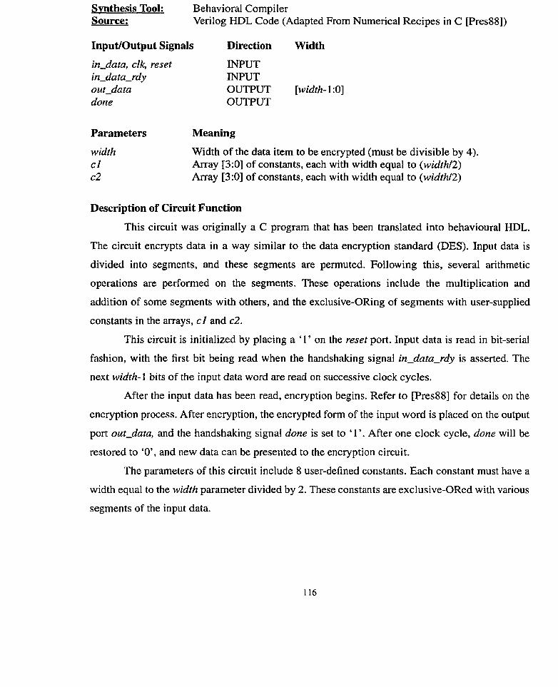
Svnthesis Tool: Behavioral Compiler Source: Verilog HDL Code (Adapted Frorn Numerical Recipes in C [Pres88])
Input/Output Signals Direction Width
in-data, clk, reset INPUT in-da ta-rdy INPUT out-data OUTPUT [width- 1 :O] done OUTPUT
Parameters Meaning
width cl c2
Width of the data item to be encrypted (must be divisible by 4). Array [3:0] of constants, each with width equal to (widthl2) Array [3:0] of constants, each with width equal to (widthl2)
Description of Circuit Function
This circuit was originally a C program that has been translated into behavioural HDL.
The circuit encrypts data in a way similar to the data encryption standard (DES). Input data is
divided into segments, and these segments are perrnuted. Following this, several arithmetic
operations are performed on the segments. These operations include the multiplication and
addition of some segments with others, and the exclusive-Oliing of segments with user-supplied
constants in the arrays, c l and c2.
This circuit is initialized by placing a ' 1' on the reset port. Input data is read in bit-serial
fashion, with the first bit being read when the handshaking signal in-data-rdy is asserted. The
next width-1 bits of the input data word are read on successive clock cycles.
After the input data has been read, encryption begins. Refer to [Pres88] for details on the
encryption process. After encryption, the encrypted form of the input word is placed on the output
port out-data, and the handshaking signal done is set to ' 1 ' . After one clock cycle, done will be
restored to 'O7, and new data can be presented to the encryption circuit.
The parameters of this circuit include 8 user-defined constants. Each constant must have a
width equal to the width parameter divided by 2. These constants are exclusive-ORed with various
segments of the input data.

wntnes~s 1001: uesign Lompiier Source: VHDL Code
Input/Output SignaIs Direction Width
in-v scan, clk out-v
INPUT [O:N- 1 ] INPUT OUTPUT [O: N- 1 ]
Parameters Meaning
N Cellular automata will be an N by N array of cells.
Description of Circuit Function
This circuit is a hardware implementation of the 'game of life' cellular automata. The
automata's structure consists of a square array of identical cells, each having connections to its
eight nearest neighbours. In a given dock cycle, a ce11 can be in the ' 1' state or the '0' state. A
cell's value in the next state (in the next clock cycle) will depend on its current state and the states
of its neighbours.
The circuit consists of two VHDL modules which must be synthesized separately. The
first describes the basic ceIl of the array and it must be compiled before the second which is a
structural module instantiating the square array of cells. The dimensions of the array are N by AT,
and therefore, the number of cells in the array is N ~ .
The states of each of the cells in the array can be initialized in N ctock cycles through the
input port in-v and the scan input. When scan is set to 'l', the value of each ce11 is simply set to
the value of its neighbour to the north. The in-v port is the array of northern connections to the top
row of cells in the array. Setting scan to 'O' causes each ceIl in the circuit to perform the game of
life algorithm.
Examining the state of al1 cells in the array is done in a way similar to the presetting of
cells. The ouf-v output port is a vector representing the states of the bottom row of cells in the
array. By setting scan equal to ' I ', the value of each ceIl in the array can eventually be passed to
the bottom row of the array, and examined through the out-v port.

Synthesis '1001: Design Cornprier Source: C program
Input/Output SignaIs Direction
i0, il, ... i(nin-1) clk, reset 00, 00, ..., o(n0ut-1)
INPUT INPUT OUTPUT
Parameters Meaning
nin Number of inputs to the finite state machine. nout Number of outputs of the finite state machine. nstate Number of states in the finite state machine. prob-tram Probability of adding another transition from a given state. prob-dc Probability that a given input is a 'don't care' in a transition.
Description of Circuit Function
A C program has been written to generate finite state machines randomly with any nurnber
of inputs, states, or outputs. The program produces state tables in Synopsys state table format. The
states in the machine are represented symbolically in the generated state table. This allows a user
to choose the encoding style from within the Design Compiler, for example, binary, one-hot, or
other encoding styles.
The number of transitions from a given state to other states can be adjusted through the
prob-tram parameter. When transitions are being generated from a certain state, this parameter
represents the probability that another state will be added. This implies that the number of
transitions from each state to other states follows a geometric distribution. Furthermore, in each
transition, each input must be either 'Oy, 'l ', or 'X'. The prob-dc parameter can be adjusted to
control the number of 'X's in the state table. Al1 states in generated machines will be reachabie
from the start state'. A sample DC script to synthesize this benchmark is:
{set up target and link libraries) read -format fsm fsm.st set_fsm-encoding-style onehot {or binary) reduce-fsm set-fsm_minimize true compile
1 . Asserting the reset input forces the state machine into the start state.

svntnesis moi: uesign Lompiier Source: VHDL Code
InpuUOutput Signals Direction Width
a, b, c clk z
INPUT [w idth- 1 :O] INPUT OUTPUT [(2* width) :O]
Parameters Meaning
width The datapath width of the circuit. pipe-length The number of pipeline stages in the multiply-accumulate operation (>2).
Description of Circuit Function
This circuit implements a pipelined form of the simple arithmetic function z= a b+ c. The
number of pipeline stages and the width of the datapath are represented as the parameters width
and pipe-length, respectively.
Upon examination of the HDL code, it appears as though data is being passed between the
circuit's registers in a shifter-like fashion, with al1 the combinational logic occurring in front of
the first set of pipeline registers. The reason for this is that the HDL for this circuit was written to
take advantage of a special Synopsys synthesis option, called register balancing. Register
balancing can automatically minimize the clock cycle time of a circuit by moving logic between
register boundaries. In essence, the tool will 'balance' the amount of logic in between the sets of
pipeline registers. Using a larger value for the pipe-length parameter will reduce the amount of
logic in each stage of the pipeline.
The benchmark can be compiled using the Design Compiler; however, the user should
issue the command 'set-balance-registers true' before synthesizing the design.
All of the registers in this circuit are positive-edge triggered flip-flops. Input data
presented to the circuit on the a, b, and c input ports will be captured on a rising clock edge, and
the output will become available on the z port several clock cycles later, depending on the value of
the pipe-length parameter.

Svnthesis Tool: Behavioral Compiler Source: VHDL Code
Input/Output Signals Direction WidEh
a, b, 7, INPUT [width- l :O] cmd INPUT [2 :O] clk, reset, in-data-ready INPUT out-data-ready OUTPUT
Parameters Meaning
width Datapath width of the circuit (a power of 2). log-w idth Must be set to log2width. vector-length Number of elements in each of the vectors A and B.
Description of Circuit Function
This circuit implements a vector ALU. Operations on the elements in two vectors, A and
B, may be perforrned in parallel depending on how the design is scheduled. The value placed on
the cmd port controls which operation is perforrned by the vector ALU as follows:
crnd 000 O0 1 010 O1 1 100 101 110 1 1 1
Selected O~eration Vector Addition (A + B) Vector Subtract (A - B) Barre1 Shift (A is shifted by the lower log-width bits of B ) Logical AND (A AND B) Logical OR (A OR B) Logical EXOR (A EXOR B) (NOT A) and B Logical NAND (A NAND B)
The circuit can be reset synchronously on the positive clock edge using the reset input.
After reset, the signal in-data-ready should be asserted when the first elements of the two vectors
A and B are placed on the a and b input ports, and the selected operation code is placed on the
crnd port. The first elements of vectors A and B, as well as the operation code will be read on the
rising edge of the clock. The subsequent vector-length-l elements will be read in successive
clock cycles. After the computation is complete, out-data-ready will be asserted for
vector-length clock cycles, with a different elernent of the result vector Z appearing on output
port z in each clock cycle.

Table E.l compares the number of logic blocks needed to implement circuits in the
CX2001 LPGA [CEC96a] with the number of blocks needed in the proposed architectures. The
numbers in the table were computed by deterrnining a ratio for each benchmark circuit and
averaging the ratios across al1 benchmarks. Thus, each circuit (whether small or large) was treated
equally. Only the combinational portion of each circuit was considered in the comparisonl. The
table shows that one combined foldable PLA-style logic block with the parameters (8, 8,4) has a
logic capacity approximately equivalent to ten CX2001 logic blocks. One foldable LUT-based
logic block with K = 5 and L = 4 is approximately equivalent to three CX2001 blocks.
Table E.l: Comparing Number of Logic Blocks
Architecture
Unfoldable PLA-based (8, 8, 3)
Table E.2 compares the total number of connected logic block pins in circuits
implemented in the proposed architectures with the number of connected pins in circuits
implemented in the CX2001. The metric of total number of connected pins has been shown to
correlate well with routing resource area [Hill9 l][Brow92] [He94]. Soth input and output logic
block pins are included in the comparison. The table shows that when circuits are implemented in
a combined foldable (8, 8,4) PLA-based architecture, they possess 5 1 % fewer connected pins, on
average, than when implemented in the CX2001. This suggests that an LPGA with such combined
foldable PLA-style logic blocks would need significantly less routing resource area than the
CX2001. Circuits implemented in a foldable LUT-based architecture with K = 5 and L = 4 have
28% fewer connected pins than when implemented in the CX2001.
Average Ratio (NCX2001/Narch)
5.93
Combined foldable PLA-based (8 ,8 ,4)
Unfoldable LUT-based (K = 4)
FoIdable LUT-based (K = 5, L = 4)
1 . This was necessary because CX2001 logic blocks contain no flip-flops.
9.89
1.80
3.14

Table E.2: Comparing Number of Connected Pins
Architecture 1 Average Ratio ( P i n ~ , , ~ f f i n s ~ ~ ~ )
UnfoIdable PLA-based (8 ,8 ,3 )
Combined foldable PLA-based (8 ,8 ,4 )
UnfoIdable LUT-based (K = 4)
Foldable LUT-based (K = 5, L. = 4)
0.53
0.49
0.8 1
0.72

APPLIED - A IMAGE, Inc - - 1653 East Main Street - -. - Rochester, NY 14609 USA -- -- - - Phone: 7161482-0300 -- -- - - Fax: 7161288-5989
0 1993. Applied Image. Inc., All Righls Resewed