application of low melt alloys as compliant thermal
TRANSCRIPT
Application of Low Melt Alloys as Compliant Thermal Interface Materials: A Study of
Performance and Degradation under Thermal Duress
by
Chandan Kumar Roy
A dissertation submitted to the Graduate Faculty of
Auburn University
in partial fulfillment of the
requirements for the Degree of
Doctor of Philosophy
Auburn, Alabama
August 6, 2016
Keywords: Thermal interface material, Thermal conductivity; Thermal resistance; Thermal
aging; Thermal cycling
Copyright 2016 by Chandan Kumar Roy
Approved by
Daniel K. Harris, Chair, Associate Professor, Mechanical Engineering
Roy W. Knight, Assistant Professor, Mechanical Engineering
Daniel Mackowski, Associate Professor, Mechanical Engineering
Bertram Zinner, Associate Professor, Mathematics and Statistics
Vishwani Agrawal, Professor, Electrical and Computer Engineering
ii
Abstract
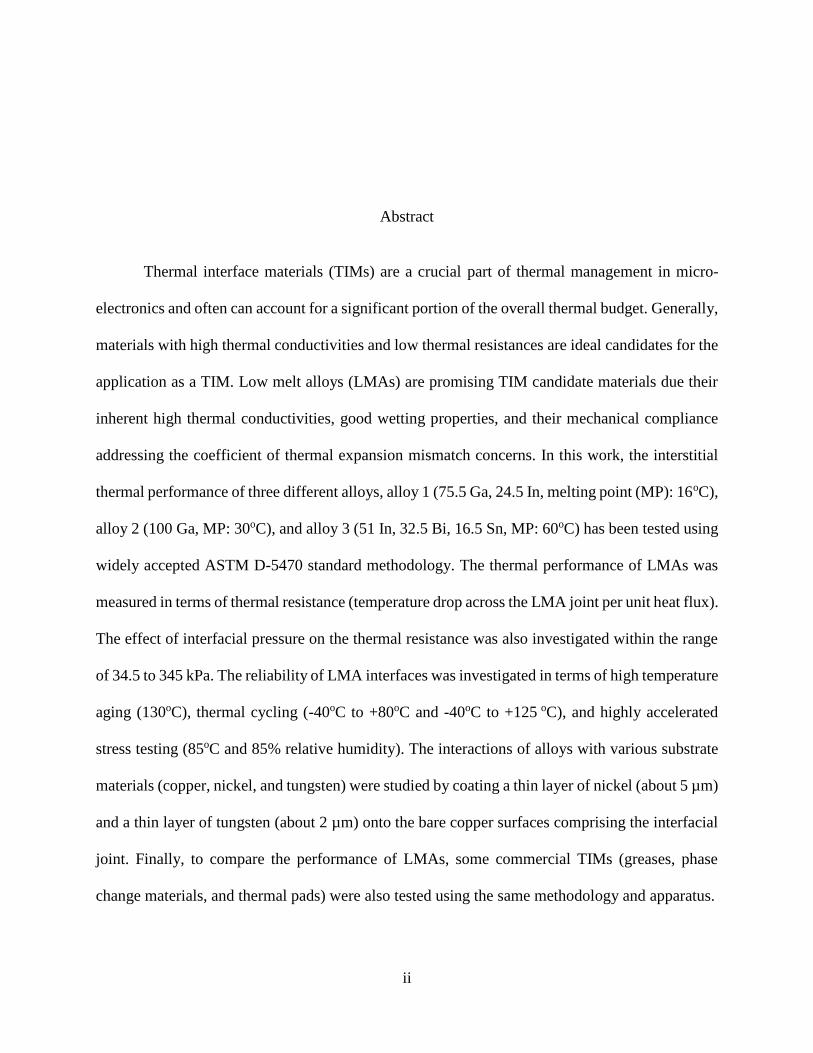
Thermal interface materials (TIMs) are a crucial part of thermal management in micro-
electronics and often can account for a significant portion of the overall thermal budget. Generally,
materials with high thermal conductivities and low thermal resistances are ideal candidates for the
application as a TIM. Low melt alloys (LMAs) are promising TIM candidate materials due their
inherent high thermal conductivities, good wetting properties, and their mechanical compliance
addressing the coefficient of thermal expansion mismatch concerns. In this work, the interstitial
thermal performance of three different alloys, alloy 1 (75.5 Ga, 24.5 In, melting point (MP): 16oC),
alloy 2 (100 Ga, MP: 30oC), and alloy 3 (51 In, 32.5 Bi, 16.5 Sn, MP: 60oC) has been tested using
widely accepted ASTM D-5470 standard methodology. The thermal performance of LMAs was
measured in terms of thermal resistance (temperature drop across the LMA joint per unit heat flux).
The effect of interfacial pressure on the thermal resistance was also investigated within the range
of 34.5 to 345 kPa. The reliability of LMA interfaces was investigated in terms of high temperature
aging (130oC), thermal cycling (-40oC to +80oC and -40oC to +125 oC), and highly accelerated
stress testing (85oC and 85% relative humidity). The interactions of alloys with various substrate
materials (copper, nickel, and tungsten) were studied by coating a thin layer of nickel (about 5 µm)
and a thin layer of tungsten (about 2 µm) onto the bare copper surfaces comprising the interfacial
joint. Finally, to compare the performance of LMAs, some commercial TIMs (greases, phase
change materials, and thermal pads) were also tested using the same methodology and apparatus.
iii
Acknowledgments
I would like to thank my advisory committee Dr. Roy Knight, Dr. Daniel Mackowski, Dr.
Bertram Zinner and Dr. Vishwani Agrawal.
It is an honor for me to thank my advisor and mentor Dr. Daniel Harris for providing me
the opportunity to work in this project and believing in me. His proper guidance and amicable
disposition encouraged me all the time throughout my dissertation work. Without his support, this
work would not have been possible.
I would like to thank Dr. Roy Knight and Dr. Sushil Bhavnani for their important
suggestions and feedback during this research.
Finally, I would like to thank my family members specially my wife and parents. Without
their love and encouragement, I could not able to continue my study.
iv
Table of Contents
Abstract ........................................................................................................................................... ii
Acknowledgments.......................................................................................................................... iii
List of Tables ............................................................................................................................... viii
List of Figures ................................................................................................................................ ix
List of Abbreviations ................................................................................................................... xiii
Chapter 1 : Introduction .................................................................................................................. 1
1.1 Thermal interface material ............................................................................................... 1
1.2 Contact resistance ............................................................................................................. 2
1.3 Thermal resistance to heat conduction ............................................................................. 3
1.4 Performance of TIM ......................................................................................................... 4
1.5 Application of TIM in thermal management.................................................................... 5
Chapter 2 : Literature Review ......................................................................................................... 7
2.1 Traditional TIMs .............................................................................................................. 7
2.1.1 Thermal grease .......................................................................................................... 7
2.1.2 Phase change material ............................................................................................... 8
2.1.3 Thermal gel ............................................................................................................... 9

v
2.1.4 Thermal pad .............................................................................................................. 9
2.2 Emerging TIMs .............................................................................................................. 10
2.2.1 Carbon-based TIMs ................................................................................................ 10
2.2.2 Low melt alloys....................................................................................................... 12
2.2.3 Other promising TIMs ............................................................................................ 18
2.3 Performance comparison ................................................................................................ 18
Chapter 3 : Experimental .............................................................................................................. 20
3.1 Materials ......................................................................................................................... 20
3.2 Thermal conductivity measurement ............................................................................... 21
3.3 Thermal resistance measurement ................................................................................... 22
3.4 Description of the apparatus used .................................................................................. 24
3.5 Test rig modification ...................................................................................................... 25
3.6 Diffusion barrier layers .................................................................................................. 27
3.7 Sample preparation ......................................................................................................... 27
3.8 Uncertainty analysis ....................................................................................................... 28
Chapter 4 : Commercial TIMs ...................................................................................................... 33
4.1 Thermal conductivity measurement ............................................................................... 33
4.2 Thermal resistance measurement ................................................................................... 34
4.2.1 Thermal grease ........................................................................................................ 34
4.2.2 Phase change material ............................................................................................. 37
vi
4.2.3 Thermal pad ............................................................................................................ 42
4.2.4 Testing of indium heat spring ................................................................................. 49
4.3 Overall performance comparison ................................................................................... 51
4.4 Summary of commercial TIMs testing........................................................................... 52
Chapter 5 : Performance of LMAs ................................................................................................ 54
5.1 Thermal conductivity measurement ............................................................................... 54
5.2 Thermal resistance measurements .................................................................................. 55
5.3 Repeatability................................................................................................................... 56
5.4 Effect of interfacial pressure .......................................................................................... 57
5.5 Effect of interface temperature ....................................................................................... 58
5.6 Reliability testing (phase 1)............................................................................................ 59
5.6.1 Accelerated thermal aging ...................................................................................... 59
5.6.2 Thermal cycling ...................................................................................................... 68
5.7 Reliability testing (phase 2)............................................................................................ 79
5.7.1 Accelerated thermal aging ...................................................................................... 80
5.7.2 Thermal cycling ...................................................................................................... 81
5.8 Reliability testing (phase 3)............................................................................................ 83
5.8.1 HAST (highly accelerated stress test) ..................................................................... 83
5.8.2 Thermal cycling (-40oC to +125oC) ........................................................................ 85
5.9 Bond line thickness ........................................................................................................ 86
vii
5.10 Issues with LMAs........................................................................................................... 87
5.10.1 LMA Containment .................................................................................................. 87
5.10.2 LMA De-wetting ..................................................................................................... 88
5.11 Cost consideration .......................................................................................................... 90
Chapter 6 : Summary and Conclusions ......................................................................................... 92
6.1 Future works ................................................................................................................... 94
Bibliography ................................................................................................................................. 96
Appendix ..................................................................................................................................... 104
viii
List of Tables
Table 3.1: Properties of the LMAs with melting temperature ranges from 16oC to 60oC ............ 20
Table 4.1: Thermal conductivity of some commercial TIMs tested using a transient thermal
conductivity analyzer .................................................................................................. 33
Table 5.1: Thermal conductivity of Ga-In alloy at room temperature .......................................... 54
Table 5.2: Repeatability of the thermal resistance measurement at 138 kPa ................................ 57
Table 5.3: Thermal resistances of In-Bi-Sn alloy (sheet and molten) at different interface
temperatures ................................................................................................................ 59

ix
List of Figures
Figure 1.1: (a) A magnified view of bare contact between two solid surfaces (b) Contact between
two solid surfaces using a TIM .................................................................................... 2
Figure 1.2: Heat transfer and the temperature distribution through a plane wall ........................... 3
Figure 1.3: Interfacial thermal resistance between two solid objects after the application of TIM 4
Figure 1.4: Low and high power electronics architecture (a) low power, typically used in laptop
applications (b) high power, typically used in desktop and server applications ......... 6
Figure 2.1: Thermal performance comparison of variety of commercial TIMs, Grease [2,4-6],
PCM [2,8,11], Gel [11,12,14,15] and emerging TIMs such as CNT (direct grown
[17-19] and transferred [18,27,28]) and LMA [4,32-34,36]...................................... 19
Figure 3.1: C-Therm Tci transient thermal conductivity analyzer ............................................... 21
Figure 3.2: Schematic of a typical ASTM D5470 standard setup ................................................ 23
Figure 3.3: (a) Testing of LMA TIM using modified test rig; the cooper disks assembly with the
TIM at the interface was placed between the TIM tester surfaces (b) Schematics of
the modified test setup ............................................................................................... 26
Figure 3.4: (a) Bare copper disks (b) Tungsten coated (2 micron) copper disk (c) Nickel coated
(5 micron) copper disks. ............................................................................................ 27
Figure 3.5: Wetting of Ga-In alloy on copper surface using a brush ............................................ 28
Figure 3.6: Copper disks assembly with probes inserted in the holes .......................................... 29
Figure 3.7: Probe disturbance as a function of thermal resistance of the TIM for perfectly aligned
probes ......................................................................................................................... 30
Figure 3.8: Probe disturbance as a function of probe location for a TIM of thermal resistance
0.01cm2oC/W ............................................................................................................. 31
x
Figure 3.9: Temperature distribution on the top surface of the TIM (a) without probes
(ΔT=0.002oC) (b) probes are perfectly aligned (ΔT=0.04oC) (c) probes are at 90o
(bottom probe is rotated) (ΔT=0.26oC) (d) probes are at 180o (ΔT=0.26oC) ............ 31
Figure 4.1: Thermal resistance as a function of applied pressure for different greases (note that
bare junction resistance values are off scale: 2.5 to 1 cm2°C/W) .............................. 35
Figure 4.2: Thermal resistance comparison of Arctic Silver 5 grease with the data provided by
Wasniewski et al. [7] ................................................................................................. 36
Figure 4.3: Comparison of measured thermal resistance of ShinEtsu X23-7921-5 grease with the
manufacturer data ...................................................................................................... 37
Figure 4.4: Thermal resistance as a function of applied pressure for different PCMs ................. 38
Figure 4.5: Thermal resistance as a function of interface temperature for Laird tech. Tpcm 588
and Tpcm 5810 with and without initial melting ....................................................... 39
Figure 4.6: Thermal resistance as a function of interface temperature for Berg. 565U ............... 40
Figure 4.7: Thermal resistance as a function of pressure at different interface temperatures for
Bergquist 565U .......................................................................................................... 41
Figure 4.8: Thermal resistance of Bergquist sil pad A2000 as a function of pressure. ................ 42
Figure 4.9: Thermal resistance of Bergquist sil pad (A2000) as a function of pressure for five
samples. ..................................................................................................................... 43
Figure 4.10: Thermal resistance as a function of interface temperature for sil pad A2000 .......... 44
Figure 4.11: Repeated test of Bergquist Sil Pad A2000. .............................................................. 45
Figure 4.12: Thermal resistance of gap pad 5000S35 as a function of pressure, compared with
manufacturer data and Wasniewski et al. [7] ............................................................ 46
Figure 4.13: Thermal resistance as a function of pressure for five samples of gap pad ............... 47
Figure 4.14: Repeated test of Bergquist gap pad 5000S35 ........................................................... 48
Figure 4.15: Effect of interface temperature for gap pad 5000S35 .............................................. 49
Figure 4.16: Thermal resistance of Indium 4(100In) heat spring ................................................. 50
Figure 4.17: Repeated test of Indium 4 (100 In) heat spring ........................................................ 50
Figure 4.18: Performance comparison of various commercial TIMs ........................................... 52
xi
Figure 5.1: In situ thermal resistances of different substrate-alloy combinations ........................ 56
Figure 5.2: Thermal resistances of Ga-In, Ga, and In-Bi-Sn alloy as a function of applied
pressure ...................................................................................................................... 58
Figure 5.3: Thermal resistances of In-Bi-Sn alloy between different substrate surfaces in
response to isothermal aging at 130oC [51] ............................................................... 61
Figure 5.4: Thermal resistances of Ga between different substrate surfaces in response to
isothermal aging at 130oC [51] .................................................................................. 63
Figure 5.5: Thermal resistances of Ga-In alloy between different substrate surfaces in response to
isothermal aging at 130oC .......................................................................................... 64
Figure 5.6: Thermal resistances of commercial TIMs in response to isothermal aging at 130oC 65
Figure 5.7: Normalized thermal resistance of three alloys placed between bare copper surfaces in
response to thermal aging at 130oC [54] .................................................................... 66
Figure 5.8: Normalized thermal resistance of three alloys placed between nickel surfaces in
response to thermal aging at 130oC ........................................................................... 67
Figure 5.9: Normalized thermal resistance of three alloys placed between tungsten surfaces in
response to thermal aging at 130oC ........................................................................... 68
Figure 5.10: Interface temperature of the copper disks assembly and chamber air temperature for
2 cycles (240 minutes) ............................................................................................... 69
Figure 5.11: Thermal cycling (-40oC to +80oC) of In-Bi-Sn alloy between different substrate
surfaces [51] ............................................................................................................... 72
Figure 5.12: Thermal cycling(-40oC to +80oC) of Ga between different substrate surfaces ........ 73
Figure 5.13: Thermal cycling (-40oC to +80oC) of Ga-In alloy between different substrate
surfaces ...................................................................................................................... 75
Figure 5.14: Thermal cycling (-40oC to +80oC) of Liquid Ultra and ShinEtsu grease between
bare copper surfaces [51] ........................................................................................... 76
Figure 5.15: Normalized thermal resistance of three alloys placed between bare copper surfaces
in response to thermal cycling (-40oC to +80oC) ....................................................... 77
Figure 5.16: Normalized thermal resistance of three alloys placed between nickel surfaces in
response to thermal cycling (-40oC to +80oC) ........................................................... 78

xii
Figure 5.17: Normalized thermal resistance of three alloys placed between tungsten surfaces in
response to thermal cycling (-40oC to +80oC) ........................................................... 79
Figure 5.18: Isothermal aging (130oC) performance of Ga-In, Ga, and In-Bi-Sn alloys between
copper and nickel surfaces [55] ................................................................................. 81
Figure 5.19: Thermal cycling (-40 to +80oC, 2 hours/cycle) of Ga-In, Ga and In-Bi-Sn alloys
between copper and nickel surfaces [55] ................................................................... 83
Figure 5.20: HAST results of three alloys between copper surfaces at 85oC and 85% RH ......... 84
Figure 5.21: Thermal cycling (-40oC to +125oC) of three alloys placed between bare copper disks
................................................................................................................................... 86
Figure 5.22: SEM cross-sectional image of Ga-In alloy placed between bare copper disks without
any shims or thickness controller [54] ....................................................................... 87
Figure 5.23: In-B-Sn alloy (a) 102 µm thick sheet after melting (b) molten state application ..... 88
Figure 5.24: In-Bi-Sn alloy (a) After 500 cycles, poorly wetted (b) A completely wetted surface
................................................................................................................................... 89
Figure 5.25: Pure Ga between bare copper after 200 cycles, one side wetting ............................ 90

xiii
List of Abbreviations
BLT Bond Line Thickness
CNT Carbon Nanotube
CTE Coefficient of Thermal Expansion
HAST Highly Accelerated Stress Testing
IHS Integrated Heat Spreader
IMC Intermetallic Compound
LMA Low Melt Alloy
MWCNT Multi-walled Carbon Nanotube
PCM Phase Change Material
PEG Polyethylene Glycol
RSD Relative Standard Deviation
RT Room Temperature
TIM Thermal Interface Material
Symbols
A Area (m2)
d Distance (m)
I Current (amp)
k Thermal Conductivity (W/moC)

xiv
L Thickness (m)
l Location of Probe (mm)
q Heat Flow (W)
q" Heat Flux (W/cm2)
R Thermal Resistance (cm2oC/W)
T Temperature (oC)
U Uncertainty
V Electric Potential (Volts)
Subscripts
avg Average
cond Conduction
th Thermal

1
Chapter 1 : Introduction
1.1 Thermal interface material
When two solid surfaces are brought into contact, surface asperities (roughness, flatness)
limit their actual contact to 1-2% of the apparent contact at a lower pressure [1]. The remaining
interspace is filled mostly with air which has a poor thermal conductivity (0.026 W/moC at room
temperature). A magnified bare contact between two solid surfaces is shown in Figure 1.1a. Heat
transfer across these solid contacts would result in significant temperature drop at the interface.
By improving the quality of these contacts, the heat transfer can be enhanced. One option is to
apply a very high pressure, which would crush much of the peaks and increase the area of contact;
however, the application of pressure is somewhat restricted considering the load constraints of the
components attached [2]. Furthermore, mating surfaces can be polished to a high degree to remove
much of the roughness and waviness. This is not a good option from an economic point of view
because the surface preparation would make the components expensive. Another feasible option
is to place a highly conductive material at the interface, which would fill those gaps at a lower
pressure by displacing air from the interface as shown in Figure 1.1b. This material, which is
placed at the interface between two objects to facilitate the heat transfer, is known as thermal
interface material (TIM). An ideal TIM would fill all the microscopic irregularities that exist at the
interface. However, an actual TIM will leave some air gaps at the interface depending on the
conformability of the TIM.

2
(a) (b)
Figure 1.1: (a) A magnified view of bare contact between two solid surfaces (b) Contact between
two solid surfaces using a TIM
1.2 Contact resistance
Contact resistance arises due the incomplete contact between two solid objects. Because of
the insufficient contact (mostly due to the surface asperities), the heat transfer at the interface is
hindered. Heat can transfer in two ways through such interface. One way is the conduction through
the actual contact points and the other way is the conduction and/or radiation through the gaps.
Thus, the contact resistance is viewed as the equivalent of two parallel resistances due to two heat
flow paths [3]. In general, rough and non-flat surfaces induce more contact resistance compared
to the smooth and flat surfaces. As such, the contact resistance can be minimized by increasing the
area of contact, which in turn enhances the heat transfer.
TIM

3
1.3 Thermal resistance to heat conduction
It is well known that for one dimensional, steady state heat transfer in a plane wall with
no internal heat generation and constant thermal conductive, the temperature varies linearly with
the distance as shown in Figure 1.2 [3]. The Fourier’s law can be written as
Figure 1.2: Heat transfer and the temperature distribution through a plane wall
𝑞 = −kAdT
dx= kA
T1 − T2
L (1-1)
Where: k is the thermal conductivity of the wall material, A is the area available for heat transfer,
T1 and T2 are the temperature of the wall, and L is the thickness of the wall. From the Fourier’s
law, the thermal resistance to heat conduction (Rcond) is defined as
Rcond =L
Ak=
T1 − T2
q (1-2)
The conduction resistance is analogous to electrical resistance for flow of current. The
conduction resistance arises due to the finite thermal conductivity of the material through which
heat flows. The material resist the flow of heat depending on its thermal conductivity.
T1
T2
q
𝐿
𝐴𝑘
T1 T2
x
L
4
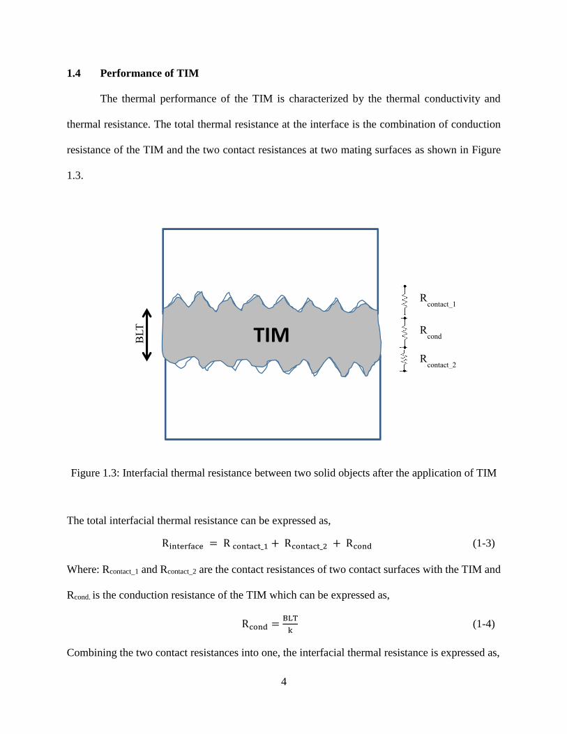
1.4 Performance of TIM
The thermal performance of the TIM is characterized by the thermal conductivity and
thermal resistance. The total thermal resistance at the interface is the combination of conduction
resistance of the TIM and the two contact resistances at two mating surfaces as shown in Figure
1.3.
Figure 1.3: Interfacial thermal resistance between two solid objects after the application of TIM
The total interfacial thermal resistance can be expressed as,
Rinterface = R contact_1 + Rcontact_2 + Rcond (1-3)
Where: Rcontact_1 and Rcontact_2 are the contact resistances of two contact surfaces with the TIM and
Rcond. is the conduction resistance of the TIM which can be expressed as,
Rcond =BLT
k (1-4)
Combining the two contact resistances into one, the interfacial thermal resistance is expressed as,
BL
T
Rcontact_1
Rcontact_2
Rcond
TIM

5
Rinterface = R contact +BLT
k (1-5)
Where: k is the thermal conductivity of the TIM and bond line thickness (BLT) is the thickness of
TIM under operation. The ultimate goal is to find a TIM material that is compatible, reliable and
offers lower interfacial thermal resistance. It is evident from the above relation (1-5) that a high
conductivity material at a thin BLT would lower conduction resistance. For this reason, it is always
expected for a TIM to be highly conductive and have a thin BLT. The contact resistances are highly
dependent on the quality of the mating surfaces (surface roughness, flatness). In general, a rough,
non-flat surface would result in a high contact resistance. In addition, the contact resistances also
are a function of how well the TIM flows at the interface, filling the microscopic voids and other
irregularities.
A desirable TIM should offer low thermal resistance at a thin BLT, high thermal
conductivity, conformability at low to moderate pressures, good wetting properties, ease of
manufacturing, and reasonable cost while also being environmentally and health friendly [2]. In
addition to these properties, compliant TIMs must also be able to withstand the mechanical stresses
resulting from the coefficient of thermal expansion (CTE) mismatches that occur between the
adjoining materials (e.g. silicon-copper for processor-heat sink attachment). If the CTE strain
overwhelms the mechanical properties of the TIM, the joint will ultimately fail. Therefore, high
performing compliant TIMs are an essential design option for better thermal performance and
improved reliability.
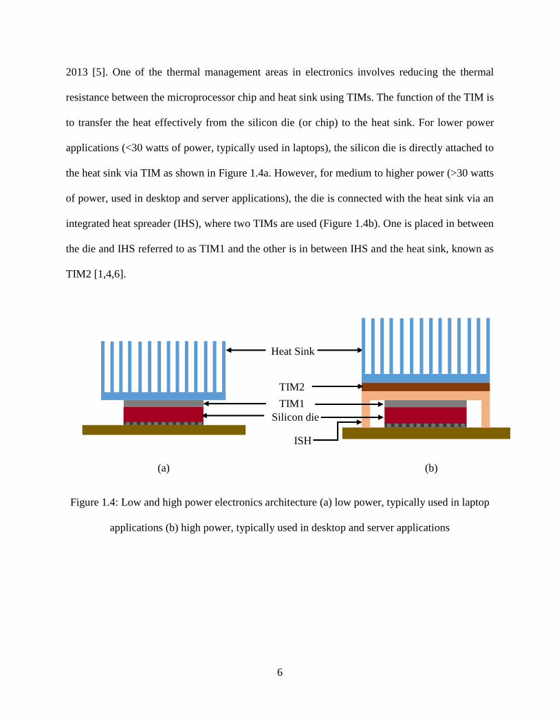
1.5 Application of TIM in thermal management
Thermal management plays a key role in electronics cooling as the power density continues
to escalate and is expected to exceed 100 W/cm2 (1 W/mm2) [4].Therefore, international
electronics manufacturing initiative (iNEMI) declared thermal management a research priority in
6
2013 [5]. One of the thermal management areas in electronics involves reducing the thermal
resistance between the microprocessor chip and heat sink using TIMs. The function of the TIM is
to transfer the heat effectively from the silicon die (or chip) to the heat sink. For lower power
applications (<30 watts of power, typically used in laptops), the silicon die is directly attached to
the heat sink via TIM as shown in Figure 1.4a. However, for medium to higher power (>30 watts
of power, used in desktop and server applications), the die is connected with the heat sink via an
integrated heat spreader (IHS), where two TIMs are used (Figure 1.4b). One is placed in between
the die and IHS referred to as TIM1 and the other is in between IHS and the heat sink, known as
TIM2 [1,4,6].
(a) (b)
Figure 1.4: Low and high power electronics architecture (a) low power, typically used in laptop
applications (b) high power, typically used in desktop and server applications
TIM1
Heat Sink
Silicon die
TIM2
ISH
7
Chapter 2 : Literature Review
2.1 Traditional TIMs
In this section, thermal performance and practical concerns of conventional TIMs such as
thermal grease, phase change material, thermal gel, and thermal pad are discussed.
2.1.1 Thermal grease
Greases are usually made by mixing silicone or hydrocarbon oil with conductive particles
such as silver, zinc oxide, aluminum oxide, or boron nitride to enhance the thermal conductivity.
Greases flow quite well at the interface and fill most of the interstitial voids and irregularities
which would otherwise be filled with air. Traditional greases have thermal resistance ranging from
0.1 to 0.55 cm2oC/W [1,7]. Today’s high performing grease such as ShinEtsu X23-7921-5, has a
thermal conductivity >6 W/moC [8] and can offer thermal resistance as low as 0.065 cm2oC/W [8].
Dow Corning claimed the thermal resistance of their grease, TC 5026, to be as low as 0.032
cm2oC/W; however, Wasniewski et al. [7] found the thermal resistance of the same compound to
be about 0.2 cm2oC/W at a thickness of 38 µm. Gwinn and Web [2] reported thermal resistance of
Arctic Silver grease was 0.018 cm2oC/W. However, Wasniewski et al. [7] and Roy et al. [8] could
not reproduce that result with the same grease; the reported thermal resistance was about 0.1
cm2oC/W. Thus, there is a large discrepancy between the manufacturer’s claimed resistance and
experimental results by different investigators. Chung [9] reported that polyethylene glycol (PEG)
based thermal pastes are superior to silicone-based pastes due to the low viscosity of PEG. PEG-

8
based paste can offer thermal resistance as low as 0.053 cm2°C/W when mixed with boron nitride
particles (optimum concentration was found as 18 vol.%). Although greases offer low thermal
resistance, there are practical concerns with greases. Greases are messy, difficult to apply and
remove during re-work, and have reliability issues such as pump out, phase separations, and dry
out, which limit the use of greases as an efficient TIM over a nominal lifespan of use [1,2]. In
addition, greases can be electrically conductive; excess grease that extrudes out of the interface
can cause electrical shorts [2].
2.1.2 Phase change material
Phase change materials (PCMs) are made of highly conductive particles suspended in a
base material, which can be a natural material such as fully refined paraffin, a polymer, a co-
polymer, or a combination of these [10]. PCMs soften and start to flow above a certain temperature.
The temperature at which the phase change occurs is called the phase change temperature or the
transition temperature. When the temperature is below the transition point, PCMs act like solid
materials, and above the transition point, the materials start to flow like greases as they begin to
fill the irregularities exist at the interface. The typical phase change temperature of the commercial
PCMs ranges from 50-90oC [10]. Gwinn and Web [2] reported the thermal resistance of PCMs
was in the range 0.14-0.58 cm2oC/W, while Blezie [11] reported in the range 0.3-0.7 cm2oC/W.
Honeywell claimed the thermal resistance of their PCM (PTM 6000 & PTM 5000) to be as low as
0.07 cm2oC/W. Roy et al. [12,13] reported the thermal resistance of Laird Tech. Tpcm 585 and
Tpcm 5810 to be about 0.10 cm2oC/W and 0.16 cm2oC/W, respectively, at 345 kPa (50 psi). In
general, PCMs have lower thermal conductivity and higher thermal resistance compared to the
greases. Besides, PCMs can form a strong bond with the mating substrates, which hinder them
from being applied between sophisticated components.

9
2.1.3 Thermal gel
Typically, gels consist of silicone oil, a cross-linker, and thermally conductive particles
[14]. Gels have similar properties to greases before being cured. However, gels are cured to a
partially cross-linked structure, which keeps them from pump-out and migration from the interface
like greases. Blazie [11] reported that the thermal resistance of gels falls in the range 0.4-0.8
cm2oC/W. Roy et al. [12] reported the thermal resistance of Chomerics Gel 30 was about 0.3
cm2oC/W. Samson et al. [15] reported the thermal resistance of an undisclosed gel to be as low as
0.1 cm2oC/W. Since gels are cured, they do not flow like greases and thus cannot offer thermal
resistance as low as the greases. In addition, delamination (due to the CTE mismatch of mating
substrates) is a major concern with gels [14].
2.1.4 Thermal pad
Thermal pads are composed of silicone or other similar elastomers loaded with thermally
conductive ceramic particles, and may include a woven fiberglass or dielectric film reinforcement
to improve handling [11]. Pads are easy to apply and remove and can be reused. They don’t suffer
from “pump-out” or “dry-out’ problem as the greases do [16]. However, their thermal performance
are not as good as greases, PCMs, and gels. In addition, moderate to high pressure is required to
conform to the mating surfaces. Thermal resistance ranges from 1-3 cm2oC/W [11]. Wasniewski
et al. [7] and Roy et al. [8] reported the thermal resistance of a Bergquist Gap pad 5000S35 was
in the range 0.82-0.90 cm2oC/W at 345 kPa, whereas, the reported thermal resistance of a Bergquist
Sil pad A2000 was about 1.65 cm2oC/W at 345 kPa [12].

10
2.2 Emerging TIMs
In this section, thermal performance and practical concerns of developing TIMs such as
carbon nanotube, graphene, low melt alloys, metallic nanospring are discussed.
2.2.1 Carbon-based TIMs
Carbon-based materials such as carbon nanotubes (CNTs), can be used directly [7,17-19]
or as a filler in composites [20-23] and graphene [24,25] have been investigated by many
researchers as TIMs due to the extremely high thermal conductivity these materials. The reported
thermal conductivity values are as high as 6600 W/moC [26], 3000 W/moC [19], 2000 W/moC [24]
for individual single-walled, multi-walled CNTs, and graphene respectively. The lowest reported
thermal resistance of MWCNTs was about 0.01 cm2°C/W [19]. Researchers found that the dry
contact between the CNTs and the mating substrate produced higher overall thermal resistance.
This problem was addressed by using a solder [19] or a commercial TIM (PCM) [17] at the free
ends of CNTs. Xu and Fisher [17] found the thermal resistance of dry contact of CNT arrays (Cu-
CNT-Si) to be about 0.198 cm2oC/W at 0.445 MPa (65 psi). However, they found that the addition
of a PCM attached to the free end of CNT array (Cu-PCM-CNT-Si) substantially reduced the
thermal resistance. At 0.35 MPa, the lowest resistance recorded was 0.052 cm2oC/W, while the
lowest resistance recorded for the PCM compound without CNTs was 0.162 cm2oC/W under the
same pressure [17]. Tong et al. [19] reported the thermal resistance was about 0.01 cm2oC/W
when CNT free-end was welded to the substrate via a thin indium layer. Even though anomalous
increase in thermal conductivity of the composite was observed when CNTs were mixed with oil
[20, 21], Fabris et al. [22] did not report any notable improvement in thermal resistance after
mixing CNTs with commercial grease (Arctic Silver 5) and silicone oil.

11
One of the issues concerning the use of CNT films as TIMs includes the extremely high
temperature (>600oC) [27] needed for CNT fabrication since those temperatures do not allow for
direct synthesis onto electronic devices. Another concern is the weak adhesion between the CNTs
and their original substrate [27]. Not only does the poor bond between the CNTs and growth
substrate contribute significantly to the thermal resistance at that interface, but it also affects long-
term functionality. Zhu et al. [27] focused on resolving those problems by developing a CNT
transfer process in their study, which was dubbed “CNT transfer technology.” With that CNT
transfer technology, Zhu et al. [27] reported the thermal resistance of CNT arrays was 0.43
cm2°C/W. Cross et al. [18] reported the thermal resistance of transferred and bonded CNT array
as low as 0.1 cm2°C/W. Barako et al. [28] reported the thermal resistance was in the range of 0.28-
0.71 cm2°C/W and 0.15-0.50 cm2°C/W when CNTs were bonded with indium and nanofoil,
respectively. Melissa et al. [29] found the thermal resistance of transferred vertically aligned CNT
array as 0.42 cm2°C/W at 345 kPa (50 psi). Comparing the results, it can be observed that even
though CNT transfer technology can potentially solve the high-temperature growth issue, the
interfacial resistance of transferred CNT arrays is comparatively higher compared to the direct-
grown CNTs. The CNT transfer technology is further needed to be improved to achieve a low
overall thermal resistance. In general, design complexity and higher costs are associated with
CNT-based TIMs. CNT-based TIMs have yet to appear as commercially available products.
Investigators [24,25] found that the addition of graphene to a composite increases the
thermal conductivity significantly. However, graphene-based composites have lower thermal
conductivity (10 W/moC at 5vol. % graphene [25]) compared to vertically-aligned CNTs (>200
W/moC [30]). Furthermore, no data on thermal resistance of graphene-based composites have been
reported up to this point.
12
2.2.2 Low melt alloys
Low melt alloys (LMAs) are usually alloys of gallium, indium, bismuth, & tin. The phase
change temperate depends on the composition of the alloys. For application as TIMs, the alloys
are chosen in such a way that they stay in liquid phase at the operating temperature of the
component attached. As the LMAs melt, they flow into the surface irregularities and reduce the
contact resistances. LMAs contain no organics, and thus no curing is required during application.
LMAs have high degree of thermal conductivity and superior wetting, which make them promising
TIM candidate materials. Mercury, lead and cadmium-based alloys are hazardous and usually
avoided due to their toxicity and environmental issues [16].
Several researchers [4, 8, 31-37] have encouraged using LMAs as efficient TIMs. In 1984,
Cook et al. [31] were the first to investigate the performance LMAs as TIMs. They tested the
LMAs in three different forms. First, the alloy was applied on a porous metallic structure, which
they referred as Porous Carrier. The porous structure facilitated the alloy containment. Second, the
alloy applied on both sides of a thin substrate (copper or copper-plated aluminum), which was
denoted as Solid Carrie and the third configuration was to apply the alloy as a thin sheet, which
was referred as Alloy configuration. In their study, a eutectic alloy of bismuth, lead, tin, indium
and cadmium, which had a melting temperature of 47 oC was used. The tests were conducted at 90
kPa (13 psi) and the lowest resistance achieved was 0.11 cm2oC/W with the Alloy configuration.
The bare joint (without the LMA TIM) thermal resistance was 3.12 cm2oC/W under the same
conditions. Results showed that LMA performance was an order of magnitude better than the bare
joint.
In 2002, Webb and Gwinn [32] tested the performance of LMAs using an ASTM D 5470
standard tester. They tested the thermal resistance of the alloy in molten and solid state. The molten

13
state tests were performed at 2 K above the melting point and the solid state test was carried out
below the melting point of the alloy. The reported thermal resistances of alloy 117
(44.7Bi/22.6Pb/19.1In/8.3Sn/5.3Cd) at 138 kPa (20 psi) were 0.058 cm2°C/W in molten state and
0.077 cm2°C/W. Results showed that solid state thermal resistance was about 33% higher than the
molten state resistance. Tests were also carried out at different pressure from 34.5 to 138 kPa and
results showed that thermal resistance variation was less than 5% in this pressure range, which
indicates that high contact pressures are not necessary to achieve a lower thermal resistance for
LMAs. Webb and Gwinn [32] also tested the reliability of LMAs in terms of thermal cycling. The
cycling test were carried out with alloy 117 from room temperature (RT) to 80oC at pressure of 59
kPa. Results showed that after 1000 cycles, the contact area was reduced by about 50% due to the
extrusion of the alloy from the interface, which in turn, increased the thermal resistance. Thermal
cycling test was also carried out by applying the alloy 117 on a nickel-coated copper substrate.
The copper substrate was 50 µm thick and the nickel coating was 5 µm on each side. The alloy
was tinned on the both sides of the nickel-coated copper substrate and thermally cycled from RT
to 80oC. In this case, significant performance degradation was observed. Back scatter electron
imaging was conducted and revealed that the alloy diffused into the nickel and formed intermetallic
compounds (IMCs). They concluded that alloy extrusion (due to the poor wetting) and IMCs
formation were the primary causes for the performance degradation upon thermal cycling.
However they did not attempt to improve the wetting of alloy and re-do the cycling test. They also
repeated the thermal cycling test with In-Bi-Sn alloy (51In/32.5Bi/16.5Sn) at different
temperatures, 7 K, 10 K, and 18 K above the melting point of the alloy (333 K). Their results
showed that performance of alloy degraded as the cycling temperature increased. It was concluded
14
that severe degradation in thermal performance could occur if the cycling temperature increased
20 K above the melting point of the alloy.
Hill and Strader [34] in 2006 developed a copper-LMA TIM by coating In-Bi-Sn alloy on
both sides of a 70 micron nickel plated copper disk. The total thickness of the LMA TIM was about
130 µm. Two alloys of In-Bi-Sn were used in their analysis. The melting point of the two alloys
were 60oC and 81oC. They reported the initial thermal resistance of 60oC alloy was 0.017 cm2°C/W
at 69 kPa (10 psi) and 0.015 cm2°C/W at 345 kPa (50 psi) and the thermal resistance of 81oC alloy
was 0.03 cm2°C/W at 69 kPa and 0.024 cm2°C/W at 345 kPa. They tested the reliability of their
LMA TIM by exposing the TIM into harsh environments, which included highly accelerated stress
testing (HAST) at 85oC and 85% relative humidity (RH) and thermal cycling. They observed that
when alloy melted, it came out of the interface. To prevent the alloy escaping, they increased the
size (diameter) of the TIM by 20% compared to the size of the disks and found that the oversized
TIM reduced alloy escaping and had improved performance upon HAST and thermal cycling from
-40 to 130oC. It was also found that the LMA TIM performed better between the copper surfaces
compared to the aluminum surfaces. They reasoned that the alloy had an improved wetting of
copper compared to aluminum and the IMCs were formed between copper and indium. With 60oC
alloy, they ran the thermal cycling test on a pc simulator from room temperature to 150oC at 138
kPa (20 psi). No degradation was observed after 1000 cycles. It should be noted that Web and
Gwinn [32] found significant degradation after cycling 20 K above the melting point of the alloy.
However, in their study, Hill and Strader [34] did not find any degradation after cycling 90 K
above the melting point of the In-Bi-Sn alloy. Thus, a complete understanding of the performance
of LMA TIM is missing from the literature. Hill and Strader [34] also observed that if the operating
temperate remained below the melting point of the alloy, the thermal resistance of the alloy did
15
not change (within experimental uncertainty) significantly. To facilitate the molten alloy
confinement and to prevent the oxidation of the alloy, they suggested to use a compliant gasket
around the perimeter. The gasket prevents the intrusion of the air into the interfacial region and
thus prevents oxidation of the alloy. The performance of the alloy was tested with and without the
gasket assembly and was found that the performance of the alloy with the gasket assembly was far
better than the alloy without the gasket.
Martin and Kessel [4] in 2007 reported the thermal resistance of an undisclosed liquid
metal TIM to be as low as 0.02 cm2°C/W with a thermal conductivity of 31 W/m°C. LMAs possess
high thermal conductivity (an order of magnitude higher compared to the traditional TIMs [3,5])
and they offer extremely low thermal resistance at small contact pressures (~7 kPa) and at a thin
bond line. With the application of wetting layers, no evidence of pump-out with LMA was
observed. They presented several ways to mitigate the failure of LMAs. For example, the wetting
of LMA was improved by providing direct metal to metal contact, oxidation/corrosion problem
was reduced with a hermetic containment to maintain a moisture free environment. It was also
found that the diffusion of LMA into the chip material (silicon) was too small to be an issue over
the lifetime of the product. Their reliability tests included HAST (85oC & 85% RH), aging at
125oC, thermal cycling from 10oC to 110oC and low temperature storage at -40oC. They did not
find any notable degradation with the LMA TIM upon any of the reliability testing. With LMA
TIM, they were able to show 750 W/cm2 of cooling using a heater chip coupled to a water cooled
heat sink.
In 2008, Carlberg et al. [35] developed a polymer-metal composite using a low melting
temperature alloy of In-Bi-Sn with a melting point of 60oC. The in-Bi-Sn alloy was infiltrated into
a three dimensional porous network of polymer fibers. The fibers provided the physical support
16
for the low melting temperature alloy. The thermal performance of the constructed polymer-LMA
composite TIM was tested using an ASTM D5470 standard apparatus. The tests were carried out
at different pressure ranging from 200 to 800 kPa and at different interface temperatures from 51oC
to 68oC. Results showed that the composite TIM had a thermal resistance of 0.085 cm2°C/W 800
kPa (116 psi) and about 0.11 cm2°C/W at 200 kPa and at an interface temperature of 51oC.The
thermal resistance was found to increase with interface temperature. For example, at 800 kPa, the
thermal resistance was found to increase from 0.085 cm2°C/W to 0.105 cm2°C/W as the
temperature increased from 51oC to 68oC. The increase in thermal resistance with interface
temperature was attributed to the decrease in thermal conductivity of the alloy with temperature.
It was also observed that the BLT the composite TIM reduced by about 13% as the pressure
increased from 200 kPa to 800 kPa.
Hamdan et al. [36] investigated the performance of mercury microdroplets as TIMs. The
microdroplets were fabricated by condensing mercury vapor on a gold-plated silicon die. One array
of 40/40 droplets and two arrays of 20/20 droplets were tested. The average size of the
microdroplets were 15µm (radius) for 40/40 array and 20 µm for one 20/20 array and 22 µm for
another 20/20 array. The thermal resistance of the microdroplet arrays was tested as a function of
applied load. Results showed that at a particular load, the thermal resistance of 40/40 array was
the lowest compared to the two 20/20 arrays. This was because 40/40 array had bigger area of
contact compared to the 20/20 arrays. It was also found that between two 20/20 arrays, array with
larger droplet size (22 µm) had a lower resistance compared to the array with smaller droplet size
(20 µm). Again, this was because of the larger contact area with the bigger droplet size. The
thermal resistance was found to vary from 0.085 cm2°C/W to 0.00253 cm2°C/W as the pressure
increased from 80 kPa to 2000 kPa. Even though an extremely low thermal resistance value is
17
reported with mercury droplets, however, because of the toxicity and health concerns, mercury
should be avoided unless its use is absolutely required.
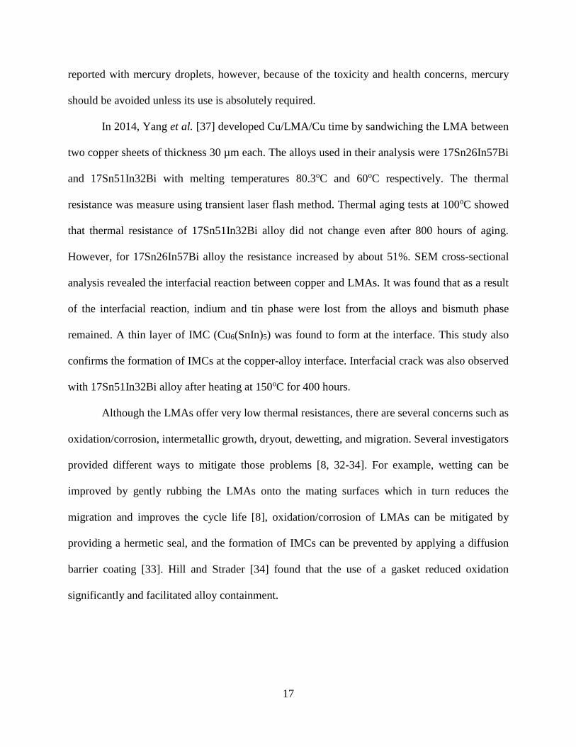
In 2014, Yang et al. [37] developed Cu/LMA/Cu time by sandwiching the LMA between
two copper sheets of thickness 30 µm each. The alloys used in their analysis were 17Sn26In57Bi
and 17Sn51In32Bi with melting temperatures 80.3oC and 60oC respectively. The thermal
resistance was measure using transient laser flash method. Thermal aging tests at 100oC showed
that thermal resistance of 17Sn51In32Bi alloy did not change even after 800 hours of aging.
However, for 17Sn26In57Bi alloy the resistance increased by about 51%. SEM cross-sectional
analysis revealed the interfacial reaction between copper and LMAs. It was found that as a result
of the interfacial reaction, indium and tin phase were lost from the alloys and bismuth phase
remained. A thin layer of IMC (Cu6(SnIn)5) was found to form at the interface. This study also
confirms the formation of IMCs at the copper-alloy interface. Interfacial crack was also observed
with 17Sn51In32Bi alloy after heating at 150oC for 400 hours.
Although the LMAs offer very low thermal resistances, there are several concerns such as
oxidation/corrosion, intermetallic growth, dryout, dewetting, and migration. Several investigators
provided different ways to mitigate those problems [8, 32-34]. For example, wetting can be
improved by gently rubbing the LMAs onto the mating surfaces which in turn reduces the
migration and improves the cycle life [8], oxidation/corrosion of LMAs can be mitigated by
providing a hermetic seal, and the formation of IMCs can be prevented by applying a diffusion
barrier coating [33]. Hill and Strader [34] found that the use of a gasket reduced oxidation
significantly and facilitated alloy containment.

18
2.2.3 Other promising TIMs
Shaddock et al. [38] proposed metallic nanospring (copper /silver) as promising TIM. The
nanospring was developed by glancing angle deposition (GLAD) process. The thermal resistance
can be achieved lower than 0.01 cm2°C/W. The idea of using nanospring is advantageous because
the nanospring structure can accommodate the CTE mismatch between silicon die and copper heat
sink. However, the fabrication of nanosprings requires precision control of deposition parameters.
In addition, the copper nanosprings are prone to oxidation and form low thermal conductivity
copper oxide, which can cause the performance degradation in actual application [38]. Luo et al.
[39] developed boron nitride nanofiber-indium composite TIM. The nanofibers were fabricated by
electrospinning process and nitridation treatment. The reported thermal resistance was <0.02
cm2°C/W at a thickness of about 25 µm.
2.3 Performance comparison
A performance comparison chart based on the previous research on a variety of TIMs is
presented in Figure 2.1. It is evident from Figure 2.1 that LMAs offer lower thermal resistance
compared to any class of material that was considered for the application as TIMs. For this reason,
this study focuses on the reliability of LMAs as efficient TIMs.

19
Figure 2.1: Thermal performance comparison of variety of commercial TIMs, Grease [2,4-6],
PCM [2,8,11], Gel [11,12,14,15] and emerging TIMs such as CNT (direct grown [17-19] and
transferred [18,27,28]) and LMA [4,32-34,36]
0
0.1
0.2
0.3
0.4
0.5
0.6
0.7
0.8
LMA CNT
(Direct grown)
CNT
(Transferred)
Grease Gel PCM
Th
erm
al
resi
stan
ce (
cm2
oC
/W)

20
Chapter 3 : Experimental
3.1 Materials
In this work, the performance of commercial TIMs and LMAs has been investigated.
Commercial TIMs include thermal grease, phase change materials, thermal pad and gels. For
LMAs, three lead and cadmium free alloys were chosen to test the thermal performance. These
alloys are primarily gallium and indium based alloys. The properties of these alloys are presented
in Table 3.1. The reasons for choosing these three alloys are that they have wide range of melting
temperatures (from 16oC to 60oC) spanning the range of interests for most application in today’s
markets and various compositions.
Table 3.1: Properties of the LMAs with melting temperature ranges from 16oC to 60oC
Alloy Composition
(% by mass)
Melting
Point (oC)
Density
(gm/cm3)
Specific Heat*
(J/goC)
1 75.5 Ga, 24.5 In 16 6.35 0.34
2 100.0 Ga 30 5.90 0.37
3 51 In, 32.5 Bi, 16.5 Sn 60 7.88 0.20
* The specific heats were calculated using Kopp-Neumann’s law [40] and densities were obtained
from the manufacturer data.

21
Spiral sensor
coil
3.2 Thermal conductivity measurement
For testing the thermal conductivity of commercial TIMs as well as LMAs, a TCi Thermal
Conductivity Analyzer (Figure 3.1) was used. A wide range of materials (solids, liquids, pastes,
and powders) can be tested both easily and nondestructively with this device. It can test over a
wide temperature range from -50°C to 200°C and can measure thermal conductivities from 0 to
120 W/moC. This device uses the modified transient plane source method to measure thermal
conductivity. A known current is supplied to the sensor’s spiral heating element, proving a small
amount of heat. This heat will rise the temperature at the interface between the season and the
sample, which results in a change in the voltage of the sensor element [41]. The rate of increase in
the sensor voltage is used to determine the thermal properties of the sample.
Figure 3.1: C-Therm Tci transient thermal conductivity analyzer
22
3.3 Thermal resistance measurement
In order to characterize the performance of the TIM, a standardized testing methodology
was needed for the current investigation. The performance of any TIM is quantified by measuring
the temperature jump across the joint (interface) per the level of heat flux travelling through the
interface. Alternatively, this can also be described as the thermal resistance of the interface. The
lower the temperature drop incurred across the thermal interface, the higher the performance of
the TIM is regarded. Obviously, for high density computing applications, TIMs with the highest
performance (lowest thermal resistance) are sought.
Several techniques such as steady state (ASTM D5470) [2,7,8,14], laser flash [37,38],
thermoreflectance [19], transient plane source (TPS), synthesized dynamic models [42],
photoacoustic [43], 3ω method [44], thermal test dies, and modified hot wire [45] are available to
quantify the thermal performance of TIMs. The method chosen for measuring the performance of
the TIMs investigated under this effort was ASTM D-5470, which is a standard, widely accepted
method for testing the thermal performance of TIMs. According to the standard [46], the testing
apparatus consists of two meter bars (hot & cold). Electrical heat is supplied through one bar as
the other bar is cooled. The sample (TIM) is placed between the meter bars. Each meter bar is
equipped with several temperature sensors to measure the drop across the sample. A typical ASTM
D5470 standard setup is presented in Figure 3.2. Several assumptions are made such as the sample
thickness being uniform at the interface and the resulting heat flow is uniform, perpendicular to
the test surfaces and purely one dimensional with no lateral heat spreading [46].
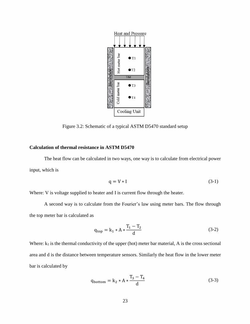
23
Figure 3.2: Schematic of a typical ASTM D5470 standard setup
Calculation of thermal resistance in ASTM D5470
The heat flow can be calculated in two ways, one way is to calculate from electrical power
input, which is
q = V ∗ I (3-1)
Where: V is voltage supplied to heater and I is current flow through the heater.
A second way is to calculate from the Fourier’s law using meter bars. The flow through
the top meter bar is calculated as
qtop = k1 ∗ A ∗T1 − T2
d (3-2)
Where: k1 is the thermal conductivity of the upper (hot) meter bar material, A is the cross sectional
area and d is the distance between temperature sensors. Similarly the heat flow in the lower meter
bar is calculated by
qbottom = k2 ∗ A ∗T3 − T4
d (3-3)

24
Where: k2 is the thermal conductivity of the lower meter bar material.
Then, the average heat flow is:
qavg =qtop + qbottom
2 (3-4)
The temperature of the hot and cold meter bar surfaces in contact with the TIM is calculated from
Ttop = T2 − d2 ∗T1 − T2
d (3-5)
Tbottom = T3 + d3 ∗T3 − T4
d (3-6)
Where: d2 is the distance between T2 and top meter bar surface in contact with TIM and d3 is the
distance between T3 and lower meter bar surface in contact with TIM. Then, the thermal resistance
of the TIM is calculated from the equation below
Rth =(Ttop − Tbottom)
(qA)
(3-7)
This thermal resistance include both the conduction resistance of the TIM as well as the contact
resistances at the top and bottom contact surfaces.
3.4 Description of the apparatus used
The thermal performances of LMA TIMs reported herein were generated using an ASTM
D5470 standard TIM tester. The tester is commercially available through Analysis Tech. The
detailed specifications of the apparatus used can be found in [47]. In this setup (Figure 3.3 a), heat
flows through the upper meter bar and the lower meter bar is cooled with a chiller. This tester uses
a linear variable differential transformer (LVDT) sensor to measure the in situ thickness of the
TIM joint. An applied pressure can be controlled from 34.5 to 2600 kPa using several different
25
pressure kits. For the testing of LMAs, a pressure sensor in the range 34.5 to 655 kPa was used
which was accurate to ±20 kPa. The electronic thickness measurement accuracy is ± 25 micron.
The test surfaces of this testing device are a highly smooth, nickel polished finish with a flatness
within 7-8 micron. The meter bars are thermally insulated to minimize the heat loss to the
surroundings. This tester operates automatically through a software called WinTIM®. The software
allows to vary the interfacial pressure and temperature of the tests.
3.5 Test rig modification
To avoid any contamination of the TIM tester surfaces and to improve the accuracy of the
test results, the LMAs were tested by placing them between copper disks. The disks are made of
alloy 110 of copper and mirror polished. The flatness of the disks was within 7-8 micron. The disks
were 3.2 mm thick and 33 mm in diameter. The resulting disks’ assembly was then placed under
the tester, shown in Figure 3.3a and 3.3b. Silicone oil (Xiameter PMX-200, viscosity: 1000CS)
was applied on the top and bottom surfaces to make a better and more reproducible contact between
the test surfaces of the TIM tester and the copper disks. The temperature differential (ΔT) across
the LMA TIM was measured by inserting two high precision thermistor probes (1 mm dia.,
accuracy 0.05oC) in a 1.2 mm diameter hole (16.5 mm deep, radius of the disk) drilled in the middle
of the copper disk. The holes were injected with thermal grease (Laird Tech. Tgrease 880) to
reduce the contact resistance of the probe in the hole.
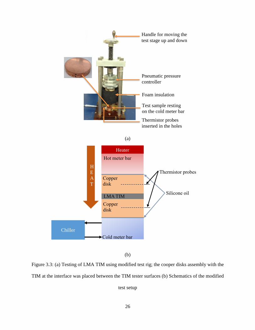
26
(a)
(b)
Figure 3.3: (a) Testing of LMA TIM using modified test rig; the cooper disks assembly with the
TIM at the interface was placed between the TIM tester surfaces (b) Schematics of the modified
test setup
Handle for moving the
test stage up and down
Pneumatic pressure
controller
Foam insulation
Thermistor probes
inserted in the holes
Test sample resting
on the cold meter bar
Copper
disk
Copper
disk
LMA TIM Silicone oil
Hot meter bar
Cold meter bar
Thermistor probes
Chiller
Heater
H
E
A
T
27
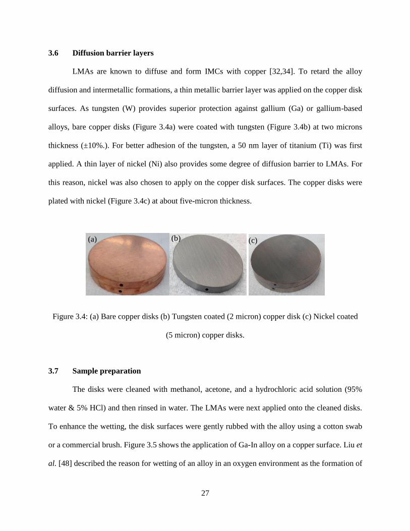
3.6 Diffusion barrier layers
LMAs are known to diffuse and form IMCs with copper [32,34]. To retard the alloy
diffusion and intermetallic formations, a thin metallic barrier layer was applied on the copper disk
surfaces. As tungsten (W) provides superior protection against gallium (Ga) or gallium-based
alloys, bare copper disks (Figure 3.4a) were coated with tungsten (Figure 3.4b) at two microns
thickness (±10%.). For better adhesion of the tungsten, a 50 nm layer of titanium (Ti) was first
applied. A thin layer of nickel (Ni) also provides some degree of diffusion barrier to LMAs. For
this reason, nickel was also chosen to apply on the copper disk surfaces. The copper disks were
plated with nickel (Figure 3.4c) at about five-micron thickness.
Figure 3.4: (a) Bare copper disks (b) Tungsten coated (2 micron) copper disk (c) Nickel coated
(5 micron) copper disks.
3.7 Sample preparation
The disks were cleaned with methanol, acetone, and a hydrochloric acid solution (95%
water & 5% HCl) and then rinsed in water. The LMAs were next applied onto the cleaned disks.
To enhance the wetting, the disk surfaces were gently rubbed with the alloy using a cotton swab
or a commercial brush. Figure 3.5 shows the application of Ga-In alloy on a copper surface. Liu et
al. [48] described the reason for wetting of an alloy in an oxygen environment as the formation of
(a) (b) (c)

28
thin oxide layer onto which LMAs wet. In the case of pure Ga, both the alloy and the disks were
heated on a hot plate above the melting point of the alloy after which the molten metal was applied
onto the heated disk’s surface by rubbing. In-Bi-Sn alloy was tested in three forms, as a four mil
(102 micron) sheet, two mil sheet (51 micron) placed between two disks and in molten form
(melted the alloy first and then applied on heated disk surfaces).
Figure 3.5: Wetting of Ga-In alloy on copper surface using a brush
3.8 Uncertainty analysis
The uncertainty in measuring thermal resistance is inversely related to the resistance value
[32]. A lower resistance value results in a higher uncertainty. Since the thermal resistances of
LMAs are expected to be relatively lower, the associated uncertainties would be higher. The
calculated uncertainty in the measurement will be represented by the error bar in all foregoing
figures representing the thermal resistance of LMAs. The details of the uncertainty analysis for the
modified testing procedure (shown in Figure 3.6) using the copper disks is presented next.
The temperatures T1 and T2 were measured with thermistors, then the temperature drop
across the TIM was calculated using the following equation:

29
q"
Figure 3.6: Copper disks assembly with probes inserted in the holes
𝛥T = Ts1 − Ts2 = T1 − T2 −2q"𝑙
k (3-8)
It is noticeable from the above equation (3-8) that the temperature drop (ΔT) across the
TIM depends on two thermistors readings (T1 and T2), heat flux (q") through the sample, thermal
conductivity (k) of the disk material, and location of the probe (l). In addition to the measurement
uncertainties, the presence of the thermistor probes in the heat flow path might disturbed the
assumed one-dimensional conduction heat flow. To quantify this disturbance, a numerical model
simulation was pursued using ANSYS, Icepak. The probe disturbance is defined as the temperature
deviation (due to presence of the probe) on the top surface of the TIM over the temperature drop
across the TIM. Figure 3.7 represents the probe disturbance as a function of thermal resistance of
the TIM placed between copper disks with stainless steel probe in the holes. Simulations were
carried out at a specified heat flow (200 watts) on the top surface and constant temperature (20oC)
at the bottom surface. It is evident from Figure 3.7 that a low resistance value results in a high
probe disturbance. Simulations were also carried out at different probe angles and it was found
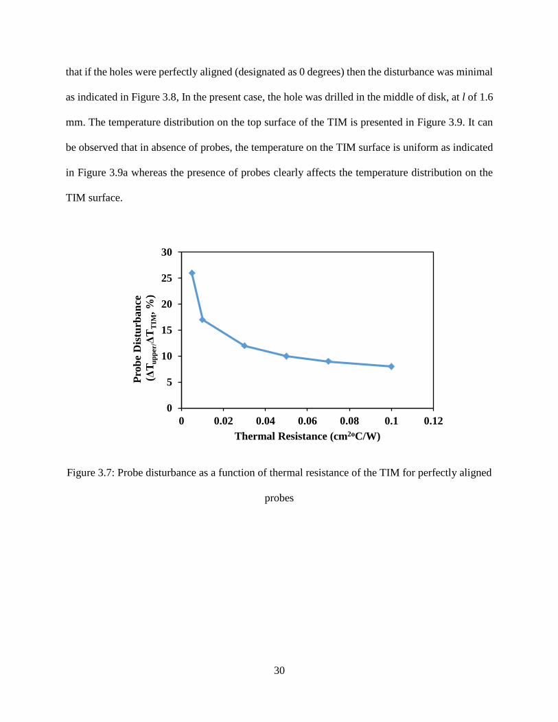
30
that if the holes were perfectly aligned (designated as 0 degrees) then the disturbance was minimal
as indicated in Figure 3.8, In the present case, the hole was drilled in the middle of disk, at l of 1.6
mm. The temperature distribution on the top surface of the TIM is presented in Figure 3.9. It can
be observed that in absence of probes, the temperature on the TIM surface is uniform as indicated
in Figure 3.9a whereas the presence of probes clearly affects the temperature distribution on the
TIM surface.
Figure 3.7: Probe disturbance as a function of thermal resistance of the TIM for perfectly aligned
probes
0
5
10
15
20
25
30
0 0.02 0.04 0.06 0.08 0.1 0.12
Pro
be
Dis
turb
an
ce
(ΔT
up
per/Δ
TT
IM, %
)
Thermal Resistance (cm2oC/W)

31
Figure 3.8: Probe disturbance as a function of probe location for a TIM of thermal resistance
0.01cm2oC/W
(a) (b) (c) (d)
Figure 3.9: Temperature distribution on the top surface of the TIM (a) without probes
(ΔT=0.002oC) (b) probes are perfectly aligned (ΔT=0.04oC) (c) probes are at 90o (bottom probe
is rotated) (ΔT=0.26oC) (d) probes are at 180o (ΔT=0.26oC)
0
50
100
150
200
250
0.6 0.8 1 1.2 1.4 1.6 1.8 2 2.2 2.4
Pro
be
Dis
turb
an
ce
(ΔT
up
per/Δ
TT
IM, %
)
Probe location, l (mm)
180 Deg. 90 Deg. 0 Deg.
32
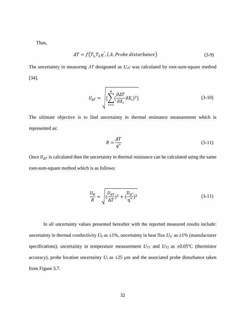
Thus,
𝛥𝑇 = 𝑓(𝑇1,𝑇2,𝑞", 𝑙, 𝑘, 𝑃𝑟𝑜𝑏𝑒 𝑑𝑖𝑠𝑡𝑢𝑟𝑏𝑎𝑛𝑐𝑒) (3-9)
The uncertainty in measuring ΔT designated as UΔT was calculated by root-sum-square method
[34].
𝑈𝛥𝑇 = √{∑(𝜕𝛥𝑇
𝜕𝑋𝑖
𝑛
𝑖=1
𝜕𝑋𝑖)2} (3-10)
The ultimate objective is to find uncertainty in thermal resistance measurement which is
represented as:
𝑅 =𝛥𝑇
𝑞" (3-11)
Once 𝑈𝛥𝑇 is calculated then the uncertainty in thermal resistance can be calculated using the same
root-sum-square method which is as follows:
𝑈𝑅
𝑅= √(
𝑈𝛥𝑇
Δ𝑇)2 + (
U𝑞"
q")2 (3-11)
In all uncertainty values presented hereafter with the reported measured results include:
uncertainty in thermal conductivity Uk as ±1%, uncertainty in heat flux Uq" as ±1% (manufacturer
specifications), uncertainty in temperature measurement UT1 and UT2 as ±0.05oC (thermistor
accuracy), probe location uncertainty Ul as ±25 µm and the associated probe disturbance taken
from Figure 3.7.

33
Chapter 4 : Commercial TIMs
4.1 Thermal conductivity measurement
Thermal conductivity is an important property of TIMs that directly affects the overall
interfacial resistance. High thermal conductivity materials provide low conduction resistances. The
thermal conductivity some commercial TIMs (thermal grease, pad) was measured using a modified
transient plane source thermal conductivity analyzer by C-Therm (Figure 3.1). Results showed that
modern greases have thermal conductivity >6 W/moC. The measured values were compared with
the manufacturer data, shown in Table 4.1. Our results are in good agreement with the
manufacturer data.
Table 4.1: Thermal conductivity of some commercial TIMs tested using a transient thermal
conductivity analyzer
Material Part Number Thermal conductivity (W/m-K)
Measured Manufacturer Spec.
Thermal grease ShinEtusu X23-7921-5 6.24 >6
Laird tech. Tgrease 880 3.64 3.1
Thermal pad Gap pad 5.08 5
Sil pad 2.7 3

34
4.2 Thermal resistance measurement
4.2.1 Thermal grease
The Figure 4.1 below presents the thermal resistance values measured as a function of
applied pressure of several commercially available high performing thermal greases. All samples
were tested at a fixed interface temperature (50oC in the present case). It is noticeable from Figure
4.1 that for any particular grease the thermal resistance decreases with the applied pressure. This
kind of behavior is expected because with any increase in pressure, more surface asperities and
voids become filled by the grease, which reduces the contact resistances. In addition, the thickness
decreases with increasing pressure, which in turn reduces the conduction resistance. However, the
change in resistance with pressure is relatively lower in this case. This is due to the thin BLT of
the greases. The thickness values measured did not vary significantly in the pressure ranges from
69 to 345 kPa. It was found that ShinEtsu X23-7921-5 thermal grease can provide a thermal
resistance as low as 0.065 cm2°C/W at 345 kPa with a bond-line of approximately 43 µm. The
uncertainty in measuring a value as low as 0.065 cm2°C/W is 10% with the test stand used. The
highest measured thermal resistance was 0.46 cm2°C/W found with Chomerics T670 grease at a
thickness of about 96 µm.
35
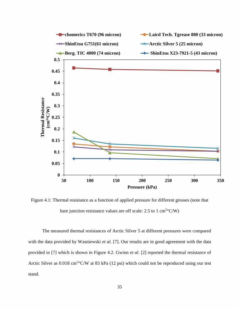
Figure 4.1: Thermal resistance as a function of applied pressure for different greases (note that
bare junction resistance values are off scale: 2.5 to 1 cm2°C/W)
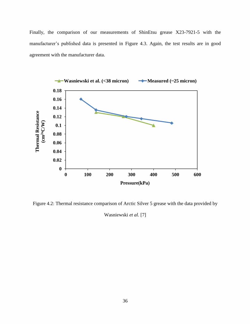
The measured thermal resistances of Arctic Silver 5 at different pressures were compared
with the data provided by Wasniewski et al. [7]. Our results are in good agreement with the data
provided in [7] which is shown in Figure 4.2. Gwinn et al. [2] reported the thermal resistance of
Arctic Silver as 0.018 cm2°C/W at 83 kPa (12 psi) which could not be reproduced using our test
stand.
0
0.05
0.1
0.15
0.2
0.25
0.3
0.35
0.4
0.45
0.5
50 100 150 200 250 300 350
Th
erm
al
Res
ista
nce
(cm
2oC
/W)
Pressure (kPa)
chomerics T670 (96 micron) Laird Tech. Tgrease 880 (33 micron)
ShinEtsu G751(61 micron) Arctic Silver 5 (25 micron)
Berg. TIC 4000 (74 micron) ShinEtsu X23-7921-5 (43 micron)
36
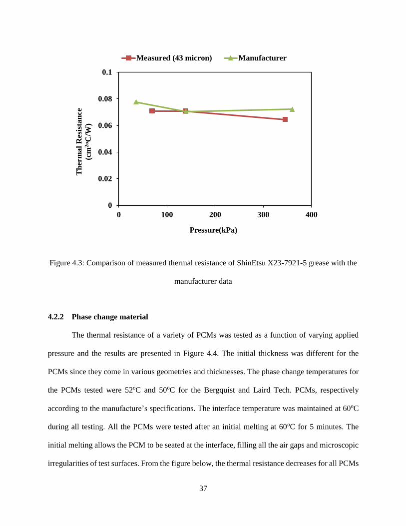
Finally, the comparison of our measurements of ShinEtsu grease X23-7921-5 with the
manufacturer’s published data is presented in Figure 4.3. Again, the test results are in good
agreement with the manufacturer data.
Figure 4.2: Thermal resistance comparison of Arctic Silver 5 grease with the data provided by
Wasniewski et al. [7]
0
0.02
0.04
0.06
0.08
0.1
0.12
0.14
0.16
0.18
0 100 200 300 400 500 600
Th
erm
al
Res
ista
nce
(cm
2oC
/W)
Pressure(kPa)
Wasniewski et al. (<38 micron) Measured (~25 micron)
37
Figure 4.3: Comparison of measured thermal resistance of ShinEtsu X23-7921-5 grease with the
manufacturer data
4.2.2 Phase change material
The thermal resistance of a variety of PCMs was tested as a function of varying applied
pressure and the results are presented in Figure 4.4. The initial thickness was different for the
PCMs since they come in various geometries and thicknesses. The phase change temperatures for
the PCMs tested were 52oC and 50oC for the Bergquist and Laird Tech. PCMs, respectively
according to the manufacture’s specifications. The interface temperature was maintained at 60oC
during all testing. All the PCMs were tested after an initial melting at 60oC for 5 minutes. The
initial melting allows the PCM to be seated at the interface, filling all the air gaps and microscopic
irregularities of test surfaces. From the figure below, the thermal resistance decreases for all PCMs
0
0.02
0.04
0.06
0.08
0.1
0 100 200 300 400
Th
erm
al
Res
ista
nce
(cm
2oC
/W)
Pressure(kPa)
Measured (43 micron) Manufacturer

38
with increasing pressure, as it is expected. Note that PCMs show a much stronger pressure
dependence when compared to the thermal greases. For example, resistance of Tpcm 585 decreases
from 0.28 cm2°C/W to 0.1 cm2°C/W (a 64 % reduction) as pressure increases from 69 to 345 kPa.
The thickness of Tpcm 585 was found to decrease from 127 µm to 64 µm (a 50% decrease) in the
same pressure range. The change in thickness of Bergquist 565U was negligible in the same
pressure range, which is why the resistance of 565U is almost invariant with pressure.
Figure 4.4: Thermal resistance as a function of applied pressure for different PCMs
Effect of initial melting
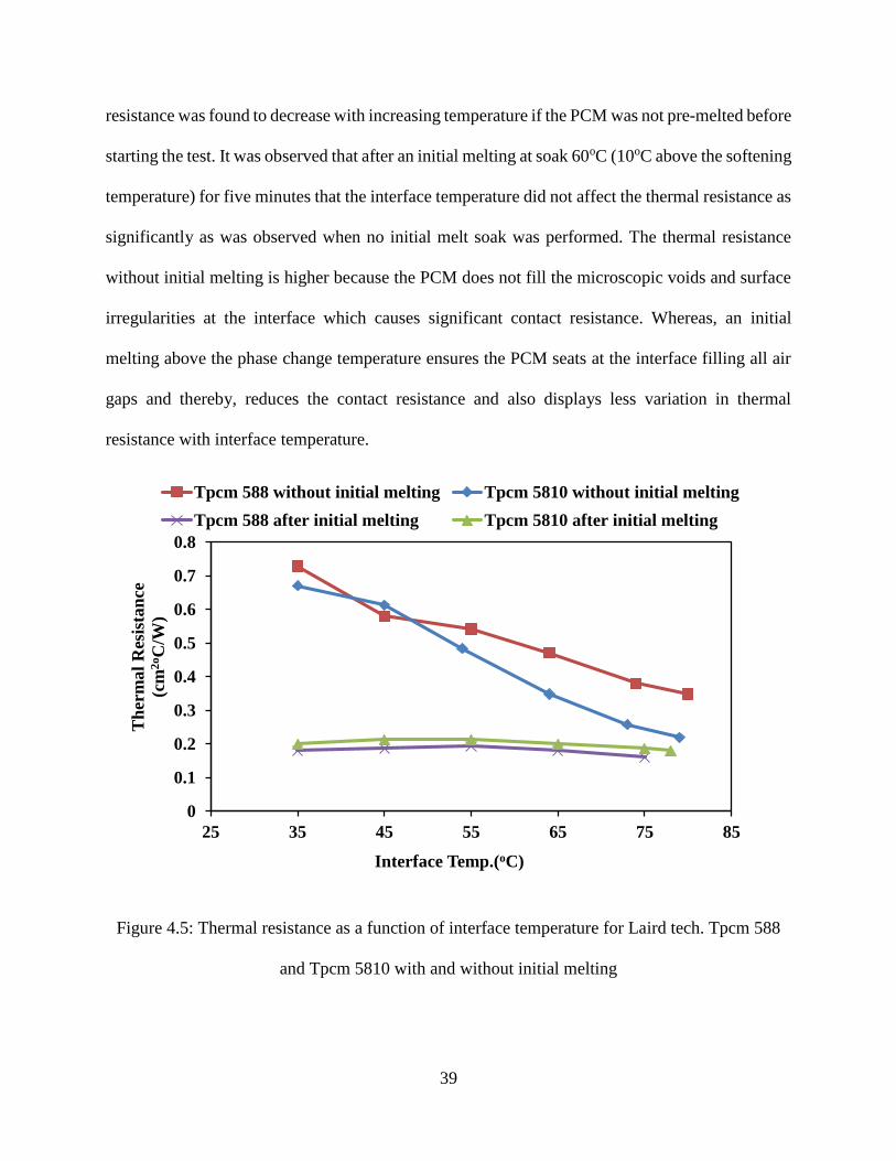
Figure 4.5 shows the thermal resistance as a function of the interface temperature for Laird
Tech. PCM 588 and 5810. The test pressure applied at the joint was 138 kPa. The thermal
0
0.1
0.2
0.3
0.4
0.5
0.6
0.7
0 50 100 150 200 250 300 350 400
Th
erm
al
Res
ista
nce
(cm
2oC
/W)
Pressure(kPa)
Berg. 565U (254 micron) Laird tech. TPCM 5810 (254 micron)
Berg. 565 UT(127 micron) Laird tech. TPCM 585 (127 micron)
39
resistance was found to decrease with increasing temperature if the PCM was not pre-melted before
starting the test. It was observed that after an initial melting at soak 60oC (10oC above the softening
temperature) for five minutes that the interface temperature did not affect the thermal resistance as
significantly as was observed when no initial melt soak was performed. The thermal resistance
without initial melting is higher because the PCM does not fill the microscopic voids and surface
irregularities at the interface which causes significant contact resistance. Whereas, an initial
melting above the phase change temperature ensures the PCM seats at the interface filling all air
gaps and thereby, reduces the contact resistance and also displays less variation in thermal
resistance with interface temperature.
Figure 4.5: Thermal resistance as a function of interface temperature for Laird tech. Tpcm 588
and Tpcm 5810 with and without initial melting
0
0.1
0.2
0.3
0.4
0.5
0.6
0.7
0.8
25 35 45 55 65 75 85
Th
erm
al
Res
ista
nce
(cm
2oC
/W)
Interface Temp.(oC)
Tpcm 588 without initial melting Tpcm 5810 without initial melting
Tpcm 588 after initial melting Tpcm 5810 after initial melting

40
The same experiments that were carried out on Tpcm materials, were also done using
Bergquist 565U. Figure 4.6 shows the effect of initial melting for Bergquist high flow 565U
(thickness 254 µm (10 mil) and phase change temperature 52oC). Different behavior was observed
with the 565 U material than that seen with the Tpcm 588 and 5810 materials. The thermal
resistance decreased until the phase change temperature was reached and then it started to increase
slightly with temperature for both cases (with and without initial melting). The thermal resistance
is higher without initial melting at every temperature. The reason could be, as explained before,
the PCM does not fill the microscopic voids and surface irregularities at the interface when no
initial melting was accomplished prior to testing.
Figure 4.6: Thermal resistance as a function of interface temperature for Berg. 565U
0
0.2
0.4
0.6
0.8
1
1.2
1.4
1.6
25 45 65 85 105
Th
erm
al
Res
ista
nce
(cm
2oC
/W)
Interface Temp.(oC)
Without initial melting With initial melting
41
Effect of interface temperature
In actual high density computing applications the interface temperature is typically not
constant. For this reason, it is important to investigate the response of a TIM at various interface
temperatures. Figure 4.7 shows the thermal resistance of Bergquist 565U as a function of pressure
at different interface temperatures. The experiments were carried out after an initial melting at
60oC for 5 minutes. It is obvious from the plot that the thermal resistance decreases with pressure
at any interface temperature. Also, the thermal resistance increases with interface temperature at
all pressures tested. For example, at 345 kPa, the thermal resistance increases from 0.48 cm2°C/W
to 0.61 cm2°C/W as the interface temperature increases from 40oC to 80oC.
Figure 4.7: Thermal resistance as a function of pressure at different interface temperatures for
Bergquist 565U
0.4
0.45
0.5
0.55
0.6
0.65
0 200 400 600 800
Th
erm
al
Res
ista
nce
(cm
2oC
/W)
Pressure(kPa)
80 deg. C 60 deg. C 40 deg. C
42
4.2.3 Thermal pad
Testing of sil pad
Bergquist A2000 sil pad is a high thermal conductivity (~3 W/m°C) silicone elastomer.
The thermal resistance of Bergquist sil pad (A2000) with initial uncompressed thickness of 381
µm (15 mil) was measured as a function of applied pressure and the results were compared with
the manufacturer as presented in Figure 4.8. The interface temperature was set at 50oC. The thermal
resistance was found to decrease from 2.10 cm2°C/W to 1.59 cm2°C/W as the pressure was
increased from 69 kPa to 690 kPa. The reason for showing this kind of behavior with increasing
pressures is as explained earlier. The change in thickness in the pressure ranges from 69-690 kPa
was found negligible (within the instrumental accuracy limit ±25 µm). The comparison shows that
in the low pressure range, the test data are not in good agreement with the manufacturer data.
However, at higher pressures agreement between measurements and manufacture’s published data
improves.
Figure 4.8: Thermal resistance of Bergquist sil pad A2000 as a function of pressure
0
0.5
1
1.5
2
2.5
3
3.5
4
0 200 400 600 800
Th
erm
al
Res
ista
nce
(cm
2oC
/W)
Pressure(kPa)
Bergquist data Measured data

43
Multiple samples testing
The pressure dependent tests of Bergquist sil pad were repeated with five different samples
to investigate the reproducibility of the test results reported. The results of the repeated tests are
shown in Figure 4.9. The maximum variation from the mean was found to be 0.15 cm2°C/W (8 %)
at 138 kPa. The test instrument’s output is adequately consistent.
Figure 4.9: Thermal resistance of Bergquist sil pad (A2000) as a function of pressure for five
samples
Effect of interface temperature
The tests were carried out at a particular pressure (345 kPa in this case) varying the
interface temperature to observe the temperature dependent characteristics of Bergquist Sil pad
A2000. Results are shown in Figure 4.10. It was found that the thermal resistance increased from
1.587 to 1.755 cm2°C/W (~11% increase) as the interface temperature increased from 35 to 85oC.
0
0.5
1
1.5
2
2.5
0 200 400 600 800
Th
erm
al
Res
ista
nce
(cm
2oC
/W)
Pressure(kPa)
sample 1 sample 2 sample 3 sample 4 sample 5

44
Figure 4.10: Thermal resistance as a function of interface temperature for sil pad A2000
Repeating test of sil pad
Figure 4.11 below shows the repeated test result for sil pad A2000 at 345 kPa. In the
repeating test mode, the same sample was tested recurrently. After each test, the sample was cooled
down for 15 minutes, and then started the test again. After thirty five repeated measurements, the
interface resistance was found to decrease from 1.66 cm2°C/W to 1.50 cm2°C/W (~10 % change).
The change in thickness was less than the instrumental accuracy (± 25 micron). According to the
manufacturer data, the thermal resistance of 15 mil A2000 sil pad at 345 kPa (50 psi) is 2.06
cm2°C/W.
1.56
1.61
1.66
1.71
1.76
1.81
35 45 55 65 75 85 95
Th
erm
al
Res
ista
nce
(cm
2oC
/W)
Interface Temp.(oC)
45
Figure 4.11: Repeated test of Bergquist Sil Pad A2000
Testing of gap pad
Bergquist 5000S35 gap pad is a soft, fiberglass reinforced highly conductive (~5 W/m°C)
thermal pad. Its’ soft consistency allows the pad to conforms to the mating surfaces. The thermal
resistance of the Bergquist 5000S35 gap pad with an initial uncompressed thickness of 508 µm
(20 mil) was measured at different pressures and the results are compared with the work of
Wasniewski et al. [7] and manufacturer’s data, and is shown in Figure 4.12. The thermal resistance
decreased from 1.02 cm2°C/W to 0.81 cm2°C/W as the pressure was increased from 69 kPa to 690
kPa. The reason is explained before. Due to the softness of this gap pad, the thickness was found
to decrease from 483 µm to 406 µm as the pressure increased from 69 kPa to 690 kPa. Comparing
the thermal resistances with the Bergquist sil pad A2000 (Figure 4.8), it can be concluded that the
performance of gap pad is superior.
0
0.4
0.8
1.2
1.6
2
0 10 20 30 40
Th
erm
al
Res
ista
nce
(cm
2oC
/W)
No. of Repeats

46
Figure 4.12: Thermal resistance of gap pad 5000S35 as a function of pressure, compared with
manufacturer data and Wasniewski et al. [7]
Multiple samples testing
The pressure dependent tests were repeated with multiple samples of the gap pad material
similar to the Sil pad tests (Figure 4.9). The maximum variation from the mean was found to be
0.065 cm2°C/W (6%) at 69 kPa.
0
0.2
0.4
0.6
0.8
1
1.2
1.4
1.6
0 200 400 600 800
Th
erm
al
Res
ista
nce
(cm
2oC
/W)
Pressure (kPa)
Manufacturer Measured Wasniewski et al.

47
Figure 4.13: Thermal resistance as a function of pressure for five samples of gap pad
Repeating tests of gap pad
This test was similar to what was conducted for the Sil pad (Figure 4.11). After thirty one
repeated measurements at 345 kPa with the same sample, the interface resistance was found to
decrease from 0.87 cm2°C/W to 0.74 cm2°C/W (15% change). Due to the softness of the gap pad,
the in-situ thickness decreased from 429 µm to 366 µm (about 15%) at 345 kPa. Thus, a 15%
decrease in thickness resulted in a 15% decrease in thermal resistance. The decrease in thermal
resistance is due to the effect of time (more air displaced), aided with the reduction in conduction
resistance (due to decrease in thickness).
0.6
0.7
0.8
0.9
1
1.1
1.2
0 200 400 600 800
Th
erm
al
Res
ista
nce
(cm
2oC
/W)
Pressure (kPa)
1st sample 2nd sample 3rd sample
4th sample 5th sample
48
Figure 4.14: Repeated test of Bergquist gap pad 5000S35
Effect of interface temperature
Figure 4.15 shows the response of the gap pad at various interfacial temperatures. It can be
concluded that the thermal performance of gap pad is not significantly affected by interface
temperature. It was found that the thermal resistance changes only by only 2% (increased from
0.92 to 0.94 cm2°C/W) as the interface temperature increased from 35 to 85oC. In the same
temperature range the sil pads’ resistance also increased by 11% (Figure 4.10).
360
370
380
390
400
410
420
430
440
0.7
0.72
0.74
0.76
0.78
0.8
0.82
0.84
0.86
0.88
0.9
0 10 20 30
Th
ick
nes
s (m
icro
n)
Th
erm
al
Res
ista
nce
(cm
2oC
/W)
No. of Repeats
Resistance Thickness

49
Figure 4.15: Effect of interface temperature for gap pad 5000S35
4.2.4 Testing of indium heat spring
Heat springs are a compressible soft metal alloy TIM (SMA-TIM) offered by Indium
Corporation of America. Indium Corporation recommended using this TIM above 241 kPa (35
psi) in order to get an acceptable thermal performance. The thermal resistance of the 102 µm (4
mil) thick indium heat spring was measured at different pressures and the results were compared
with the data provided by Indium Corporation. This comparison is shown in Figure 4.16. Again,
the thermal resistance was seen to decrease from 0.56 cm2°C/W to 0.16 cm2°C/W as the pressure
increased from 138 kPa to 690 kPa. Repeated test at 345 kPa revealed (Figure 4.17) that the thermal
resistance was reduced by around 56% (0.25 cm2°C/W to 0.11 cm2°C/W) after 31 measurements.
Again, the time under pressure is shown to be a significant factor in determining the thermal
resistance.
0.85
0.87
0.89
0.91
0.93
0.95
0.97
0.99
35 45 55 65 75 85
Th
erm
al
Res
ista
nce
(cm
2oC
/W)
Interface Temp.(oC)

50
Figure 4.16: Thermal resistance of Indium 4(100In) heat spring
Figure 4.17: Repeated test of Indium 4 (100 In) heat spring
0
0.1
0.2
0.3
0.4
0.5
0.6
0 200 400 600 800
Th
erm
al
Res
ista
nce
(cm
2oC
/W)
Pressure (kPa)
Measured Manufacturer
0
0.05
0.1
0.15
0.2
0.25
0.3
0 5 10 15 20 25 30 35
Th
erm
al
Res
ista
nce
(cm
2oC
/W)
No. of Repeats

51
4.3 Overall performance comparison
Figure 4.18 provides an overall comparison of all the commercial TIMs tested using the
same apparatus. The bare contact (without any TIM) thermal resistances are also presented for
comparison. The best performing TIM was found as the ShinEtsu X-23-7921 thermal grease. The
lowest measured thermal resistances of this grease were 0.071 cm2°C/W and 0.065 cm2°C/W at
69 and 345 kPa respectively with a thickness of 43 µm. PCMs were found as the second best
performing commercial TIM technology. They displayed a lower resistance when compared to
other TIMs except the ShinEtsu grease. The Bergquist sil pad A2000 had the highest thermal
resistance as compared to all other TIMs tested under this investigation. The gap pad showed better
performance compared to the sil pad even though the initial uncompressed thickness of the gap
pad was higher (508 µm) as compared to sil pad (381 µm ).
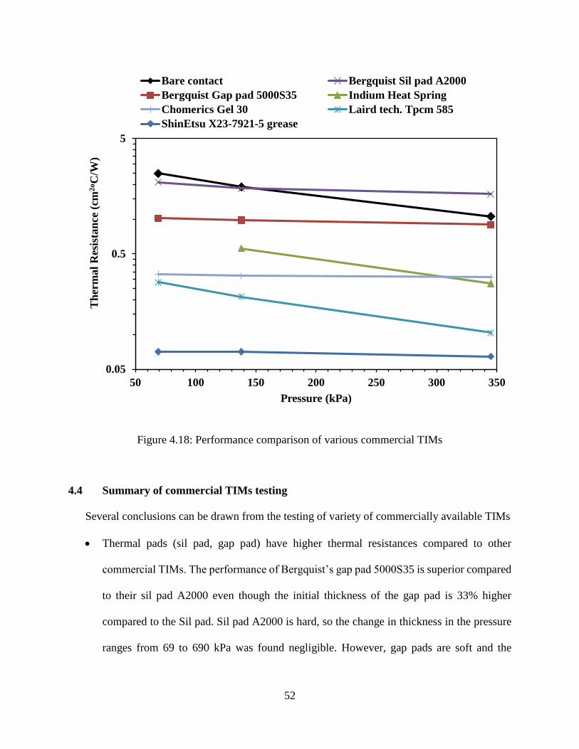
52
Figure 4.18: Performance comparison of various commercial TIMs
4.4 Summary of commercial TIMs testing
Several conclusions can be drawn from the testing of variety of commercially available TIMs
Thermal pads (sil pad, gap pad) have higher thermal resistances compared to other
commercial TIMs. The performance of Bergquist’s gap pad 5000S35 is superior compared
to their sil pad A2000 even though the initial thickness of the gap pad is 33% higher
compared to the Sil pad. Sil pad A2000 is hard, so the change in thickness in the pressure
ranges from 69 to 690 kPa was found negligible. However, gap pads are soft and the
0.05
0.5
5
50 100 150 200 250 300 350
Th
erm
al
Res
ista
nce
(cm
2oC
/W)
Pressure (kPa)
Bare contact Bergquist Sil pad A2000
Bergquist Gap pad 5000S35 Indium Heat Spring
Chomerics Gel 30 Laird tech. Tpcm 585
ShinEtsu X23-7921-5 grease
53
thickness reduces by around 15% in the same pressure range. Thermal pads are easy to
apply and remove from the interface.
Heat springs (100% In) shows better performance in the high pressure range. They are also
easy to apply and remove from the interface like thermal pads.
Repeated test results reveals that the duration that a TIM kept under pressure is a significant
factor in determining thermal resistance. For example, thermal resistance of the Indium
heat spring reduces by as much as 56% after thirty one repeated measurements at 345 kPa.
PCMs provide lower resistance compared to thermal pads and gels. But they form a strong
bond with the test surfaces upon melting which make it difficult to remove from the
interface after testing. There will be rework concerns with PCMs.
ShinEtsu X-23-7921-5 thermal grease has the lowest thermal resistance and a thinner BLT.
However, due to high the viscosity of greases, they are messy and difficult to apply and
remove from the interface. Greases do not form any chemical bonding with the test surfaces
like PCMs. Excess grease was found to extrude out from interface with the application of
higher pressure, must be cleaned to avoid any electrical shorts in actual CPU-heat sink
application.
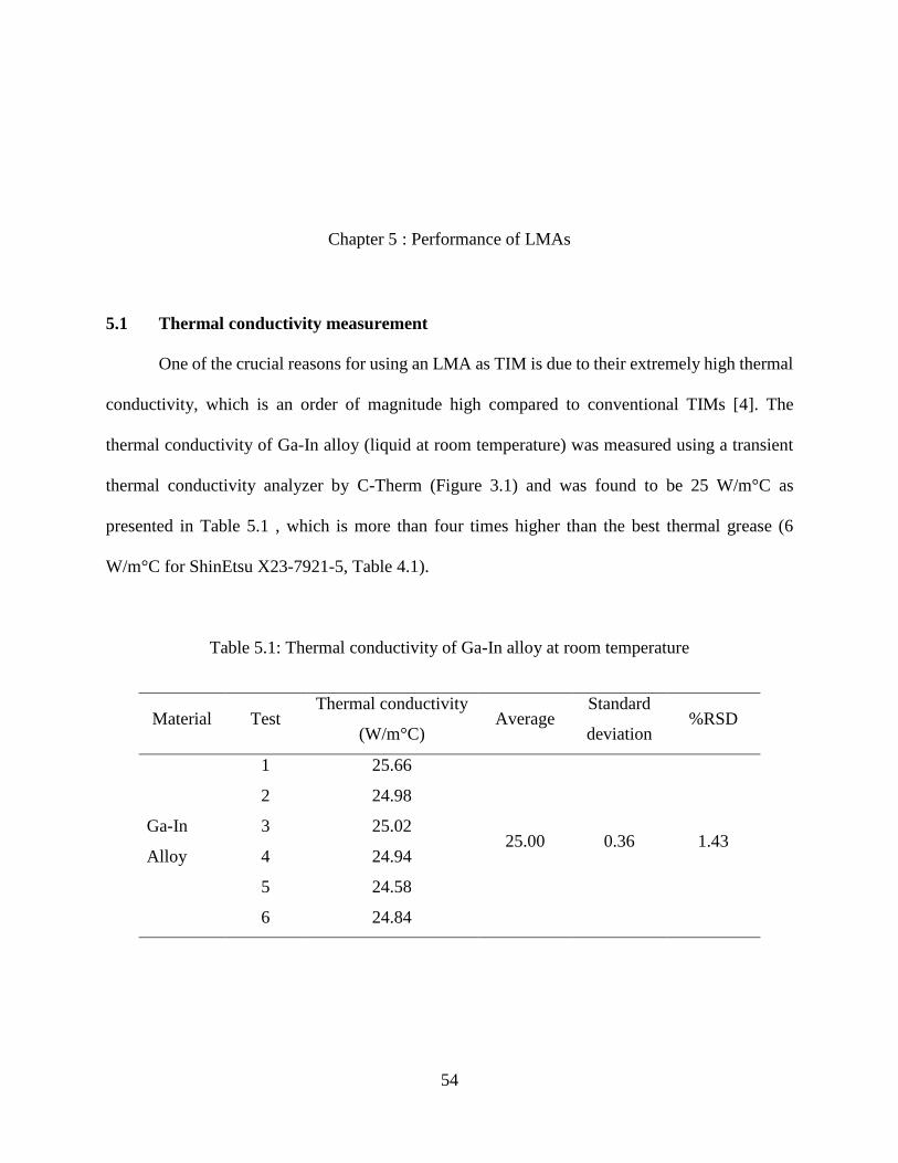
54
Chapter 5 : Performance of LMAs
5.1 Thermal conductivity measurement
One of the crucial reasons for using an LMA as TIM is due to their extremely high thermal
conductivity, which is an order of magnitude high compared to conventional TIMs [4]. The
thermal conductivity of Ga-In alloy (liquid at room temperature) was measured using a transient
thermal conductivity analyzer by C-Therm (Figure 3.1) and was found to be 25 W/m°C as
presented in Table 5.1 , which is more than four times higher than the best thermal grease (6
W/m°C for ShinEtsu X23-7921-5, Table 4.1).
Table 5.1: Thermal conductivity of Ga-In alloy at room temperature
Material Test Thermal conductivity
(W/m°C) Average
Standard
deviation %RSD
Ga-In
Alloy
1 25.66
25.00 0.36 1.43
2 24.98
3 25.02
4 24.94
5 24.58
6 24.84
55
5.2 Thermal resistance measurements
The thermal resistances of nine different substrate-alloy combinations (three alloys
between three different surfaces) tested using the modified test-rig (i.e. using the copper disks
previously described) is presented in Figure 5.1. For example, a total of five samples were tested
with In-Bi-Sn alloy between bare copper disks, designated as Cu/In-Bi-Sn/Cu. The lowest
resistance measured was 0.014 cm2°C/W, whereas the resistance also measured as high as 0.065
cm2°C/W on a separate test sample. The calculated uncertainties are represented by the error bars
in Figure 5.1. Each resistance value presented here is the average of three repeated measurements.
The measured lowest resistance was as low as 0.005 cm2°C/W with W/In-Bi-Sn/W and as high as
0.065 cm2°C/W with Cu/In-Bi-Sn/Cu. The variation in thermal resistance for the same substrate-
alloy combination results from the unique nature of each sample and points to workmanship issues.
Since LMAs are highly conductive and the joints are relatively thin, the contact resistances (mostly
due to surface irregularities such as surface roughness and flatness) dominate the interfacial
resistance. Even a small change in surface properties would result in observable changes in the
overall thermal resistance. It was assumed that all the disks had the same degree of surface
roughness and flatness, but this is not valid in reality. It should be noted that it was not possible to
maintain the exact amount of LMAs at the interface for each pair of disks during testing. Another
source of variation might appear from the manual scrubbing (wetting) of LMAs onto the disk
surfaces. During the wetting process, it was found that some samples were more easily wetted
while others required hard scrubbing to induce wetting. If the LMAs do not wet the entire surface
properly, small air pockets might be present at the interface, which in turn increases the thermal
resistance. Considering all these factors, each disks pair was different and it was a challenge to
reproduce the result even with similar substrate-alloy combination. Other properties of the alloys

56
such as viscosity, surface tension, and oxidation state during application might cause the variation
in thermal performance for different substrate-alloy combinations.
5.3 Repeatability
Table 5.2 represents the results of ten separate tests of thermal resistances on a single
sample of In-Bi-Sn alloy between bare copper disks at 138 kPa. After each test, the sample was
taken out, the silicone oil was cleaned from the surfaces, and then the sample was set back to start
another test. The measurements showed that the average thermal resistance was 0.030 cm2°C/W
with a relative standard deviation (RSD) of 5.42%. The results indicate an excellent repeatability
of the setup.
Figure 5.1: In situ thermal resistances of different substrate-alloy combinations
0
0.01
0.02
0.03
0.04
0.05
0.06
0.07
0.08
Th
erm
al
Res
ista
nce
(cm
2oC
/W)
LMAs at 138 kPa
Cu/InBi-Sn/Cu
W/In-Bi-Sn/W
Ni/In-Bi-Sn/N
i
W/G
a/W
Ni/Ga/N
i
Cu/G
a/Cu
W/G
a-In/W
Cu/G
a-In/Cu
Ni/Ga-In/N
i
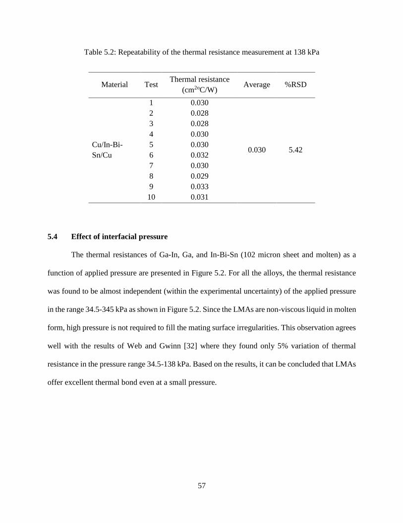
57
Table 5.2: Repeatability of the thermal resistance measurement at 138 kPa
Material Test Thermal resistance
(cm2oC/W) Average %RSD
Cu/In-Bi-
Sn/Cu
1 0.030
0.030 5.42
2 0.028
3 0.028
4 0.030
5 0.030
6 0.032
7 0.030
8 0.029
9 0.033
10 0.031
5.4 Effect of interfacial pressure
The thermal resistances of Ga-In, Ga, and In-Bi-Sn (102 micron sheet and molten) as a
function of applied pressure are presented in Figure 5.2. For all the alloys, the thermal resistance
was found to be almost independent (within the experimental uncertainty) of the applied pressure
in the range 34.5-345 kPa as shown in Figure 5.2. Since the LMAs are non-viscous liquid in molten
form, high pressure is not required to fill the mating surface irregularities. This observation agrees
well with the results of Web and Gwinn [32] where they found only 5% variation of thermal
resistance in the pressure range 34.5-138 kPa. Based on the results, it can be concluded that LMAs
offer excellent thermal bond even at a small pressure.
58
Figure 5.2: Thermal resistances of Ga-In, Ga, and In-Bi-Sn alloy as a function of applied
pressure
5.5 Effect of interface temperature
A series of tests were conducted to observe the effect of interfacial temperature on the
thermal resistance of In-Bi-Sn alloy (102 µm sheet and molten). The tests were conducted at
different interfacial temperatures in the range 35-85oC keeping the pressure constant at 69 kPa.
The results are presented in Table 5.3. The thermal resistance was found to be insensitive to the
interface temperatures tested. This study concludes that once the alloy melts and seats at the
interface, the interface temperature does not affect the performance significantly.
0
0.01
0.02
0.03
0.04
0.05
0.06
0.07
0 100 200 300 400
Th
erm
al
Res
ista
nce
(cm
2oC
/W)
Pressure(kPa)
Ga-In In-Bi-Sn Ga

59
Table 5.3: Thermal resistances of In-Bi-Sn alloy (sheet and molten) at different interface
temperatures
Interfacial
temperature
(oC)
In-Bi-Sn Alloy (102 µm sheet) In-Bi-Sn (molten)
Thermal Resistance
(cm2oC/W)
35 0.033±23% 0.037±20%
55 0.031±25% 0.039±18%
75 0.033±23% 0.039±18%
85 0.033±23% 0.037±20%
5.6 Reliability testing (phase 1)
Phase 1 reliability testing includes high temperature aging at 130oC and thermal cycling
from -40oC to +80oC. The alloys were placed between bare copper (Cu/alloy/Cu), nickel-coated
copper (Ni/alloy/Ni) and tungsten-coated copper substrates (W/alloy/W) to investigate different
substrate-alloy interactions upon thermal aging and cycling.
5.6.1 Accelerated thermal aging
Accelerated aging was carried out by exposing the disks assembly with alloys at the
interface at an elevated temperature of 130oC (followed reliability conditions of [49]) in an
atmospheric furnace (Cress electric furnace, model: C136) for extended periods of time.

60
5.6.1.1 Thermal aging of In-Bi-Sn alloy
Figure 5.3 shows the accelerated thermal aging behavior of In-Bi-Sn alloy in molten form
applied between bare copper, nickel-coated copper, and tungsten-coated copper surfaces. The tests
were carried out at 138 kPa and an interface temperature 10oC above the melting point of the alloy.
The thermal resistances are plotted as a function of aging time and the associated uncertainty is
represented by the error bars. It was found that after 1,900 hours of aging with In-Bi-Sn alloy
between bare copper surfaces (designated as Cu/In-Bi-Sn/Cu), the thermal resistance did not
change significantly (remained within the experimental uncertainty) compared to the initial
resistance. The results indicate an excellent thermal performance of In-Bi-Sn alloy between bare
copper surfaces. Yang et al. [37] did not find any degradation of the same In-Bi-Sn alloy placed
between bare copper foil after heating at 100oC for 800 hours. However, they found an interfacial
crack after heating at 150oC for 400 hours, which concludes that degradation may occur anywhere
between 130oC and 150oC. With In-Bi-Sn alloy between nickel surfaces, the resistance increased
by about 133% (from 0.024 cm2°C/W to 0.056 cm2°C/W) after 1,900 hours of aging. Even though
this seems a large percentage increase, the thermal resistance is still lower (0.056 cm2°C/W)
compared to the performance of commercial TIMs presented in chapter 4. The thermal resistance
of In-Bi-Sn alloy between tungsten-coated surfaces started to increase steadily after 576 hours (24
days). The resistance increased from 0.011 cm2°C/W to 0.032cm2°C/W after 1,900 hours of aging.
The superior aging performance of In-Bi-Sn alloy is believed to be due to the enhanced
wetting of the alloy with the substrate surface. If the alloy wets the mating surfaces properly, the
thermal performance will degrade very slowly. Since In-Bi-Sn alloy contains 51% In, it is most
likely to form IMCs with copper and nickel [32, 34, 37, 50]. Most common IMCs of In with copper
and nickel at a temperature below 130oC are Cu11In9 and In27Ni10 [50]. In addition, the growth of

61
In-Ni intermetallic is slower compared to the growth of Cu-In intermetallic (the growth rate of
Cu11In9 at 393K is 31.024*10-14 cm2/s, while the growth rate of In27Ni10 at the same temperature
is 14.976*10-14 cm2/s) [50]. Perhaps, for this reason, the thermal resistance of In-Bi-Sn alloy
between nickel surfaces increases comparatively faster than between copper surfaces upon aging.
However, due to the growth of IMCs in the interfacial region, a mechanical bond between two
disks was formed. The disks were hard to separate. Therefore, rework concerns would have to be
addressed for the combination of this alloy between bare copper.
Figure 5.3: Thermal resistances of In-Bi-Sn alloy between different substrate surfaces in
response to isothermal aging at 130oC [51]
0
0.01
0.02
0.03
0.04
0.05
0.06
0.07
0.08
0.09
0 300 600 900 1200 1500 1800
Th
erm
al
Res
ista
nce
(cm
2oC
/W)
Aging Time (hours)
Cu/In-Bi-Sn/Cu Ni/In-Bi-Sn/Ni W/In-Bi-Sn/W
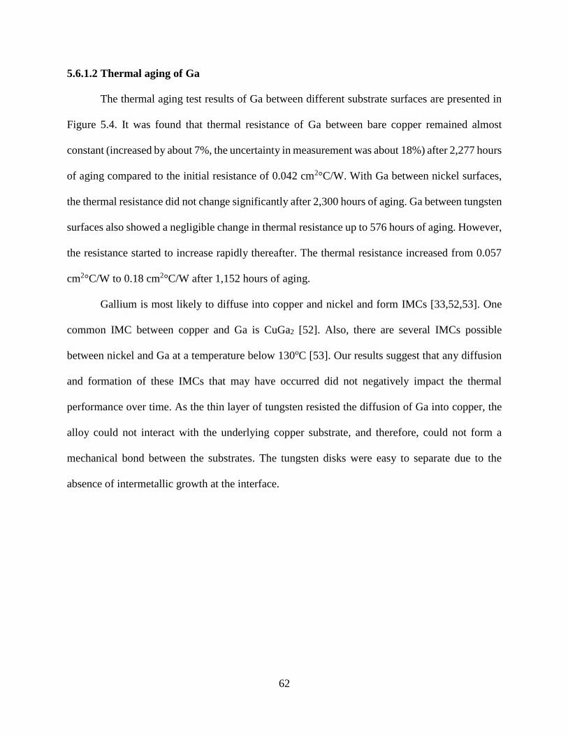
62
5.6.1.2 Thermal aging of Ga
The thermal aging test results of Ga between different substrate surfaces are presented in
Figure 5.4. It was found that thermal resistance of Ga between bare copper remained almost
constant (increased by about 7%, the uncertainty in measurement was about 18%) after 2,277 hours
of aging compared to the initial resistance of 0.042 cm2°C/W. With Ga between nickel surfaces,
the thermal resistance did not change significantly after 2,300 hours of aging. Ga between tungsten
surfaces also showed a negligible change in thermal resistance up to 576 hours of aging. However,
the resistance started to increase rapidly thereafter. The thermal resistance increased from 0.057
cm2°C/W to 0.18 cm2°C/W after 1,152 hours of aging.
Gallium is most likely to diffuse into copper and nickel and form IMCs [33,52,53]. One
common IMC between copper and Ga is CuGa2 [52]. Also, there are several IMCs possible
between nickel and Ga at a temperature below 130oC [53]. Our results suggest that any diffusion
and formation of these IMCs that may have occurred did not negatively impact the thermal
performance over time. As the thin layer of tungsten resisted the diffusion of Ga into copper, the
alloy could not interact with the underlying copper substrate, and therefore, could not form a
mechanical bond between the substrates. The tungsten disks were easy to separate due to the
absence of intermetallic growth at the interface.
63
Figure 5.4: Thermal resistances of Ga between different substrate surfaces in response to
isothermal aging at 130oC [51]
5.6.1.3 Thermal aging of Ga-In alloy
The thermal aging test results of Ga-In between different substrate surfaces are presented
in Figure 5.5. Again, Ga-In alloy (contains 74.5%Ga and 24.5%In) between copper and nickel
surfaces exhibited a superior aging behavior. With Ga-In alloy between bare copper and nickel
surfaces, the thermal resistance remained unchanged (within experimental uncertainty) after a long
aging time (2,000 hours between bare copper and 2,030 hours between nickel-coated copper).
However, the thermal resistance of Ga-In alloy between tungsten surfaces was found to increase
by about three times after 2,019 hours of aging, which indicates a non-reliable thermal joint.
0
0.02
0.04
0.06
0.08
0.1
0.12
0.14
0.16
0.18
0.2
0 300 600 900 1200 1500 1800 2100 2400 2700
Th
erm
al
Res
ista
nce
(cm
2oC
/W)
Aging Time (hours)
Cu/Ga/Cu Ni/Ga/Ni W/Ga/W

64
It can be observed that the aging behavior of Ga-In alloy (Figure 5.5) is similar to the
response of Ga (Figure 5.4). This is because both alloys have similarity in their composition, pure
gallium contains 100% Ga and Ga-In alloy contains 74.5 % Ga. Therefore, it was expected for
both alloys to behave in a similar manner. All these results suggest that interactions between the
alloy and the substrates make the joint more thermally reliable.
Figure 5.5: Thermal resistances of Ga-In alloy between different substrate surfaces in response to
isothermal aging at 130oC
0
0.05
0.1
0.15
0.2
0.25
0 300 600 900 1200 1500 1800 2100 2400
Th
erm
al
Res
ista
nce
(cm
2oC
/W)
Aging Time (hours)
Cu/Ga-In/Cu Ni/Ga-In/Ni W/Ga-In/W

65
5.6.1.4 Commercial TIMs
To compare the performance of different alloys, a commercially available liquid metal,
Liquid Ultra and thermal grease, ShinEtsu X23-7921-5, were also aged similar to the method used
to age LMAs. With the Liquid Ultra between bare copper surfaces, the thermal resistance did not
increase significantly (within experimental uncertainty) after 1000 hours of aging, as shown in
Figure 5.6. With the ShinEtsu grease, the resistance was found to increase by about 75% (from
0.08 cm2°C/W to 0.14 cm2°C/W) after 1000 hours of aging. It is well-known that the greases dry
out over time [2], which results in increased joint thermal resistances upon aging.
Figure 5.6: Thermal resistances of commercial TIMs in response to isothermal aging at 130oC
5.6.1.5 Summary of accelerated aging results
The normalized thermal resistance (found after dividing by the initial thermal resistance)
of three alloys between copper, nickel and tungsten surfaces are presented in Figure 5.7, 5.8, and
5.9 respectively. The isothermal aging results showed that the alloys between copper surfaces
0
0.02
0.04
0.06
0.08
0.1
0.12
0.14
0.16
0.18
0 500 1000
Th
erm
al
Res
ista
nce
(cm
2oC
/W)
Aging Time (hours)
ShinEtsu Grease Liquid Ultra
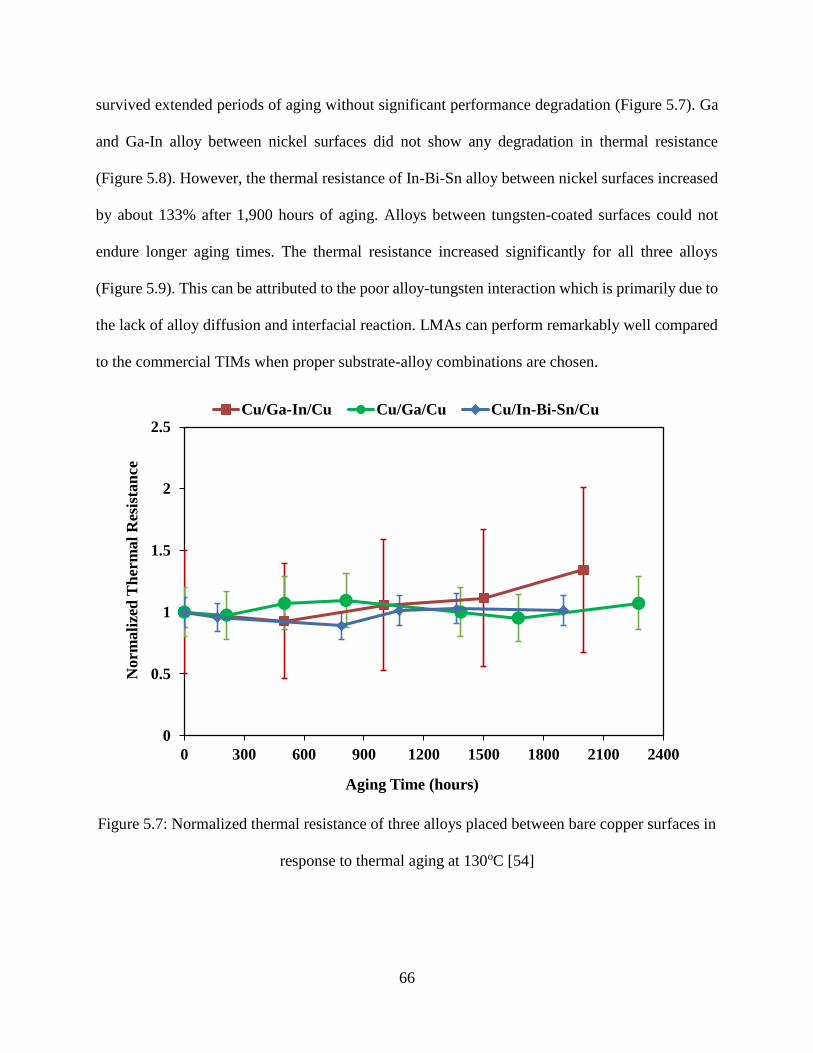
66
survived extended periods of aging without significant performance degradation (Figure 5.7). Ga
and Ga-In alloy between nickel surfaces did not show any degradation in thermal resistance
(Figure 5.8). However, the thermal resistance of In-Bi-Sn alloy between nickel surfaces increased
by about 133% after 1,900 hours of aging. Alloys between tungsten-coated surfaces could not
endure longer aging times. The thermal resistance increased significantly for all three alloys
(Figure 5.9). This can be attributed to the poor alloy-tungsten interaction which is primarily due to
the lack of alloy diffusion and interfacial reaction. LMAs can perform remarkably well compared
to the commercial TIMs when proper substrate-alloy combinations are chosen.
Figure 5.7: Normalized thermal resistance of three alloys placed between bare copper surfaces in
response to thermal aging at 130oC [54]
0
0.5
1
1.5
2
2.5
0 300 600 900 1200 1500 1800 2100 2400
Norm
ali
zed
Th
erm
al
Res
ista
nce
Aging Time (hours)
Cu/Ga-In/Cu Cu/Ga/Cu Cu/In-Bi-Sn/Cu

67
Figure 5.8: Normalized thermal resistance of three alloys placed between nickel surfaces in
response to thermal aging at 130oC
0
0.5
1
1.5
2
2.5
3
0 300 600 900 1200 1500 1800 2100 2400 2700
Norm
ali
zed
Th
erm
al
Res
ista
nce
Aging Time (hours)
Ni/Ga-In/Ni Ni/Ga/Ni Ni/In-Bi-Sn/Ni

68
Figure 5.9: Normalized thermal resistance of three alloys placed between tungsten surfaces in
response to thermal aging at 130oC
5.6.2 Thermal cycling
The purpose of these tests is to cycle each sample above and below the melting point of
the interfacial alloy. The disks assembly with alloys at the interface was placed in a thermal cycling
chamber to cycle from -40oC to 80oC [49]. The heating and cooling were performed at ramp rates
of 3oC/minute for both the heating and cooling transitions. The samples were soaked for 20 minutes
at the two extreme temperatures, ensuring that the interface reached the chamber temperature. The
time needed to complete a thermal cycle was 2 hours.
0
0.5
1
1.5
2
2.5
3
3.5
4
0 300 600 900 1200 1500 1800 2100 2400
Norm
ali
zed
Th
erm
al
Res
ista
nce
Aging Time (hours)
W/Ga-In/W W/Ga/W W/In-Bi-Sn/W
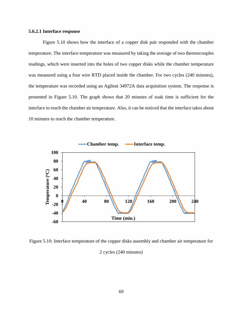
69
5.6.2.1 Interface response
Figure 5.10 shows how the interface of a copper disk pair responded with the chamber
temperature. The interface temperature was measured by taking the average of two thermocouples
readings, which were inserted into the holes of two copper disks while the chamber temperature
was measured using a four wire RTD placed inside the chamber. For two cycles (240 minutes),
the temperature was recorded using an Agilent 34972A data acquisition system. The response is
presented in Figure 5.10. The graph shows that 20 minutes of soak time is sufficient for the
interface to reach the chamber air temperature. Also, it can be noticed that the interface takes about
10 minutes to reach the chamber temperature.
Figure 5.10: Interface temperature of the copper disks assembly and chamber air temperature for
2 cycles (240 minutes)
-60
-40
-20
0
20
40
60
80
100
0 40 80 120 160 200 240
Tem
per
atu
re (
oC
)
Time (min.)
Chamber temp. Interface temp.
70
5.6.2.2 Thermal cycling of In-Bi-Sn alloy
Thermal cycling of In-Bi-Sn alloy in different forms (molten and 102 micron sheet) on
different surfaces is presented in Figure 5.11 below. It is apparent from the figure that In-Bi-Sn
alloy in its molten form (melted the alloy first and then applied on the heated disks) has an
improved thermal cycle performance when compared to its sheet application. After 1,400 cycles
(2800 hours) of In-Bi-Sn alloy between bare copper surfaces, the thermal resistance increased only
by about 22% from its initial value of 0.023 cm2°C/W (the measurement uncertainty was about
32%), while the thermal resistance of In-Bi-Sn alloy as a 102 micron (4 mil) sheet increased
significantly (by about 5.5 times) after 1,400 cycles. Roy et al. [8] discussed this reason as the
enhanced wetting of the alloy in molten form. When applied as a solid sheet, most of the alloy
came out of the interface upon melting. After the test, upon separation of the disks, it was found
that the alloy did not wet the interface properly. As a result, the alloy extruded out of the interface
due to expansion and contraction occurred upon thermal cycling, which resulted in the loss of the
contact area. For this reason, the thermal resistance increased significantly upon thermal cycling.
On the other hand, when applied in molten form, the disks were mechanically scrubbed with the
molten alloy to induce wetting. Hence, the alloys remained within the interface, no extrusion was
observed upon thermal cycling, and thereby voids could not be formed at the interface. Therefore,
the thermal resistance did not change significantly upon thermal cycling. This result agrees well
with the work of Hill and Strader [34], where no degradation of this alloy was found after running
1,000 cycles between room temperature and 150oC.
In-Bi-Sn alloy between nickel-coated surfaces was also found to perform well; after 1,400
cycles, the thermal resistance remained within the experimental uncertainty. The thermal cycling
test of In-Bi-Sn alloy between nickel surfaces was repeated with a second sample to ensure the

71
repeatability of the test results. A second sample of In-Bi-Sn alloy between nickel surfaces also
responded well to thermal cycling as shown in Figure 5.11.
Along with the alloy-substrate interaction, another factor that affects the thermal
performance of the TIM is the CTE mismatch between different substrates. Due to the CTE
mismatch, the TIM gradually extrudes out of the interface because of the expansion and
contraction occurring during thermal cycling. This phenomenon is known as the pump-out of the
TIM. Voids can be created at the interface because of this pump-out effect, which in turn increases
the thermal resistance. The CTE mismatch between copper and nickel is smaller (about 4
µm/moC). In addition to that, the diffusion of In into nickel produces a good thermal joint,
improving the performance under thermal cycling.
With In-Bi-Sn alloy between tungsten surfaces, the resistance was found to increase
significantly upon thermal cycling, which indicates the failure of the thermal joint. It is shown in
isothermal aging of In-Bi-Sn alloy between tungsten surfaces (Figure 5.3) that the thermal
resistance started to increase after certain hours (576 hours), however, during cycling, the
resistance increased significantly just after 200 cycles (400 hours). This can be attributed to the
poor alloy-tungsten interaction as well as the large CTE mismatch between copper and tungsten
(about 13 µm/moC). During the wetting process, it was found that the tungsten-coated disks
required hard scrubbing to induce wetting because the tungsten layer resisted the formation of an
oxide layer on the surface. The large CTE mismatch along with the improper wetting of the alloy
on tungsten resulted in an extrusion of the alloy from the interface upon thermal cycling, causing
the thermal resistance to increase significantly.

72
Figure 5.11: Thermal cycling (-40oC to +80oC) of In-Bi-Sn alloy between different substrate
surfaces [51]
5.6.2.3 Thermal cycling of Ga
Figure 5.12 shows thermal cycling of Ga between different substrate surfaces. The results
showed that the thermal resistance of Ga between bare copper surfaces did not change significantly
even after 1,400 cycles. However, the thermal resistance of Ga between nickel surfaces increased
by about four times (300% increase) after 1,000 cycles. With Ga between tungsten surfaces, the
thermal resistance increased significantly upon thermal cycling; it doubled for the first sample and
increased by about 4.5 times for the second sample as shown in the Figure 5.12 below. Although
Ga between nickel surfaces survived a long aging time (Figure 5.4), it failed to endure thermal
0
0.1
0.2
0.3
0.4
0.5
0.6
0
0.02
0.04
0.06
0.08
0.1
0.12
0.14
0.16
0 200 400 600 800 1000 1200 1400
Th
erm
al
Res
ista
nce
(cm
2oC
/W)
Th
erm
al
Res
ista
nce
(cm
2oC
/W)
Number of Cycles
Cu/In-Bi-Sn/Cu (102 micron sheet) Cu/In-Bi-Sn/Cu (molten)
Ni/In-Bi-Sn/Ni Ni/In-Bi-Sn/Ni (2nd sample)
W/In-Bi-Sn/W

73
cycling. This is because, during aging, the sample was kept at a constant temperature; there was
no pump-out due to expansion and contraction of the thermal joint as in thermal cycling. The
interaction between the bare copper substrate and Ga makes the thermal joint more durable. It was
found that the disks were bonded together like a solder joint. However, due to this diffusion and
bonding, the disks were hard to separate after the test.
Figure 5.12: Thermal cycling(-40oC to +80oC) of Ga between different substrate surfaces
5.6.2.4 Thermal cycling of Ga-In alloy
The thermal cycling response of Ga-In alloy between different surfaces is presented in
Figure 5.13. The tests were repeated with multiple samples to observe the repeatability of the
0
0.05
0.1
0.15
0.2
0.25
0.3
0 300 600 900 1200 1500
Th
erm
al
Res
ista
nce
(cm
2oC
/W)
Number of Cycles
Cu/Ga/Cu Ni/Ga/Ni
W/Ga/W W/Ga/W (2nd sample)

74
results. Similar to Ga, Ga-In alloy between bare copper surfaces performed very well with thermal
cycling. The thermal resistance did not change significantly for both samples even after 1,400
cycles, which indicates an excellent thermal joint. Again, this can be attributed to the interaction
(diffusion and interfacial reaction) of the Ga-In alloy (which contains 75% Ga and 25% In) with
bare copper substrate, which makes the thermal joint highly reliable. Thermal resistances of Ga-
In alloy between nickel and tungsten surfaces increased significantly after a small numbers of
cycles. The tests were repeated with multiple samples and both samples displayed the same trend,
which ensured the repeatability of the test results. It can be noticed that similar to aging, the thermal
cycling response of Ga-In alloy (Figure 5.13) is very similar to Ga (Figure 5.12). Both alloys
between bare copper survived large number of cycles (1,400). However, between nickel and
tungsten surfaces, the resistances increased significantly for both alloys.

75
Figure 5.13: Thermal cycling (-40oC to +80oC) of Ga-In alloy between different substrate
surfaces
5.6.2.5 Thermal cycling of commercial TIMs
Similar to aging, to compare the thermal cycling performance of the proposed alloys,
commercial ShinEtsu X23-7921-5 grease and Liquid Ultra were also thermally cycled by placing
between bare copper disks and the results are shown in Figure 5.14. The thermal resistance was
found to increase by about 175% after 800 cycles for ShinEtsu Grease and after 1,400 cycles for
Liquid Ultra. Comparing the performance of commercial TIMs with all three alloys, it can be
concluded that the suggested alloys performed remarkably well when placed between bare copper
disks.
0
0.05
0.1
0.15
0.2
0.25
0.3
0 300 600 900 1200 1500
Th
erm
al
Res
ista
nce
(cm
2oC
/W)
Number of Cycles
Cu/Ga-In/Cu Cu/Ga-In/Cu (2nd sample)
Ni/Ga-In/Ni Ni/Ga-In/Ni (2nd sample)
W/Ga-In/W W/Ga-In/W (2nd sample)

76
Figure 5.14: Thermal cycling (-40oC to +80oC) of Liquid Ultra and ShinEtsu grease between
bare copper surfaces [51]
5.6.2.6 Summary of thermal cycling
The normalized thermal resistances (found after dividing by the initial thermal resistance)
of three alloys between copper, nickel, and tungsten surfaces are presented in Figure 5.15, 5.16,
5.17 respectively. The thermal cycling results showed that the alloys between bare copper surfaces
survived 1,400 cycles without significant performance degradation (Figure 5.15). In-Bi-Sn alloy
between nickel surfaces did not show any degradation in thermal resistance upon thermal cycling.
However, the thermal resistance of Ga and Ga-In alloy between nickel surfaces increased
significantly after few cycles, which indicates the failure of the thermal joint (Figure 5.16). All the
alloys between tungsten-coated surfaces did not survive thermal cycling (Figure 5.17). Again, as
0
0.02
0.04
0.06
0.08
0.1
0.12
0.14
0 500 1000 1500
Th
erm
al
Res
ista
nce
(cm
2oC
/W)
Number of Cycles
ShinEtsu Grease Liquid Ultra
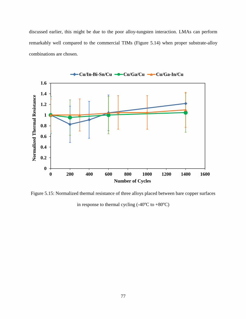
77
discussed earlier, this might be due to the poor alloy-tungsten interaction. LMAs can perform
remarkably well compared to the commercial TIMs (Figure 5.14) when proper substrate-alloy
combinations are chosen.
Figure 5.15: Normalized thermal resistance of three alloys placed between bare copper surfaces
in response to thermal cycling (-40oC to +80oC)
0
0.2
0.4
0.6
0.8
1
1.2
1.4
1.6
0 200 400 600 800 1000 1200 1400 1600
Norm
ali
zed
Th
erm
al
Res
ista
nce
Number of Cycles
Cu/In-Bi-Sn/Cu Cu/Ga/Cu Cu/Ga-In/Cu
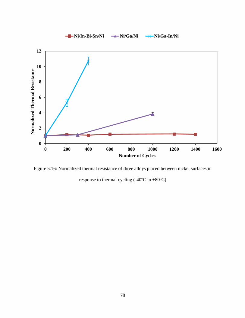
78
Figure 5.16: Normalized thermal resistance of three alloys placed between nickel surfaces in
response to thermal cycling (-40oC to +80oC)
0
2
4
6
8
10
12
0 200 400 600 800 1000 1200 1400 1600
Norm
ali
zed
Th
erm
al
Res
ista
nce
Number of Cycles
Ni/In-Bi-Sn/Ni Ni/Ga/Ni Ni/Ga-In/Ni

79
Figure 5.17: Normalized thermal resistance of three alloys placed between tungsten surfaces in
response to thermal cycling (-40oC to +80oC)
5.7 Reliability testing (phase 2)
In phase 1 reliability testing described above, the alloys were placed between similar
materials (Cu-alloy-Cu, Ni-alloy-Ni and W-alloy-W). In phase 2 testing, the alloys were placed
between copper and nickel surfaces (Cu-alloy-Ni) to investigate the reliability of alloys at the
interface between dissimilar materials. Then, the alloys were exposed to high temperature aging
and thermal cycling as before.
0
2
4
6
8
10
12
0 200 400
Norm
ali
zed
th
erm
al
resi
stan
ce
Number of cycles
W/In-Bi-Sn/W W/Ga/W W/Ga-In/W
80
5.7.1 Accelerated thermal aging
Figure 5.18 shows the accelerated thermal aging (at 130oC) behavior of three alloys (Ga-
In, Ga, and In-Bi-Sn) placed between copper and nickel surfaces. All tests were carried out at 138
kPa (20 psi) and at a temperature above the melting point of the alloy. The thermal resistances are
plotted as a function of aging time and the associated uncertainty is represented by the error bars.
It can be noticed from Figure 5.18 that all three alloys offer very low initial thermal resistance and
survived as long as 3,000 hours of aging at 130oC without significant performance degradation.
The results indicate that the proposed alloys are remarkably reliable at the interface between copper
and nickel in terms of high temperature aging. For the Ga-In alloy, a jump in thermal resistance
was observed between 1,000-1,500 hours. However, the resistance did not change thereafter
(remained within the experimental uncertainty), between 1,500-3,000 hours. The thermal
resistance is still lower compared to the performance of any existing commercial TIMs [7,8,12]
after such a prolonged exposure to high temperature.
As described above, the superior aging performance of all three alloys is believed to be due
to the enhanced wetting of the alloy with the substrate surface and the alloy-substrate interactions.
These results suggest that any diffusion and formation of IMCs that may have occurred did not
negatively impact the thermal performance over time. However, it was difficult to separate the
disks due to the growth of IMCs in the interfacial region. Therefore, rework concerns need to be
addressed.
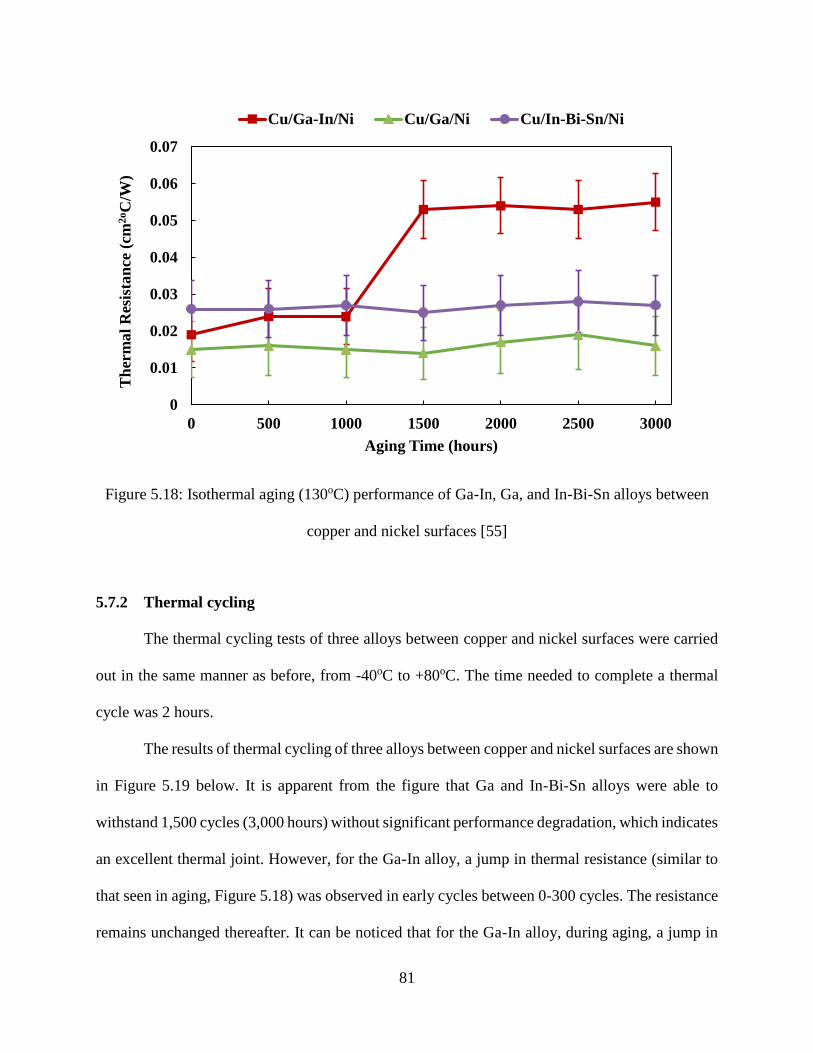
81
Figure 5.18: Isothermal aging (130oC) performance of Ga-In, Ga, and In-Bi-Sn alloys between
copper and nickel surfaces [55]
5.7.2 Thermal cycling
The thermal cycling tests of three alloys between copper and nickel surfaces were carried
out in the same manner as before, from -40oC to +80oC. The time needed to complete a thermal
cycle was 2 hours.
The results of thermal cycling of three alloys between copper and nickel surfaces are shown
in Figure 5.19 below. It is apparent from the figure that Ga and In-Bi-Sn alloys were able to
withstand 1,500 cycles (3,000 hours) without significant performance degradation, which indicates
an excellent thermal joint. However, for the Ga-In alloy, a jump in thermal resistance (similar to
that seen in aging, Figure 5.18) was observed in early cycles between 0-300 cycles. The resistance
remains unchanged thereafter. It can be noticed that for the Ga-In alloy, during aging, a jump in
0
0.01
0.02
0.03
0.04
0.05
0.06
0.07
0 500 1000 1500 2000 2500 3000
Th
erm
al
Res
ista
nce
(cm
2oC
/W)
Aging Time (hours)
Cu/Ga-In/Ni Cu/Ga/Ni Cu/In-Bi-Sn/Ni
82
thermal resistance was observed between 1000-1500 hours; however, in cycling, the jump
occurred within 600 hours (300 cycles). The expedited jump during cycling can be attributed to
the expansion and contraction of the thermal joint in cycling, which causes the degradation to start
earlier compared to aging, where the sample kept at constant temperature. Even with the jump in
thermal resistance for Ga-In alloy, the performance is still superior to the existing commercial
TIMs [7,8,12].
It can be noticed from phase 1 reliability testing that the thermal resistance of Ga and Ga-
In alloys when cycled between two nickel surfaces increased significantly (Figure 5.16). However,
no degradation was observed for those alloys when cycled between two bare copper surfaces
(Figure 5.15). In phase 2 testing, no significant degradation was observed with Ga and Ga-In alloys
after cycling between copper and nickel surfaces (Figure 5.19). These results indicate that the
alloys interact well with copper, which is primarily due to the diffusion and interfacial reaction.
For this reason, when the alloys are in contact with copper at the interface, a more durable thermal
joint is formed.

83
Figure 5.19: Thermal cycling (-40 to +80oC, 2 hours/cycle) of Ga-In, Ga and In-Bi-Sn alloys
between copper and nickel surfaces [55]
5.8 Reliability testing (phase 3)
Phase 3 reliability testing includes highly accelerated stress testing at 85oC and 85%
relative humidity and thermal cycling from -40oC to +125oC. The alloys were placed between bare
copper (Cu/alloy/Cu) surfaces and then carried out the reliability testing.
5.8.1 HAST (highly accelerated stress test)
HAST was carried out by exposing the disks assembly with alloys at the interface at 85oC
and 85% relative humidity (RH) for extended periods of time.
Figure 5.20 shows the HAST test results of three alloys (Ga-In, Ga, and In-Bi-Sn) applied
between bare copper disk surfaces. All tests were carried out at a temperature above the melting
0
0.01
0.02
0.03
0.04
0.05
0.06
0.07
0.08
0 500 1000 1500
Th
erm
al
Rei
stan
ce (
cm2
oC
/W)
Number of Cycles
Cu/Ga-In/Ni Cu/Ga/Ni Cu/In-Bi-Sn/Ni
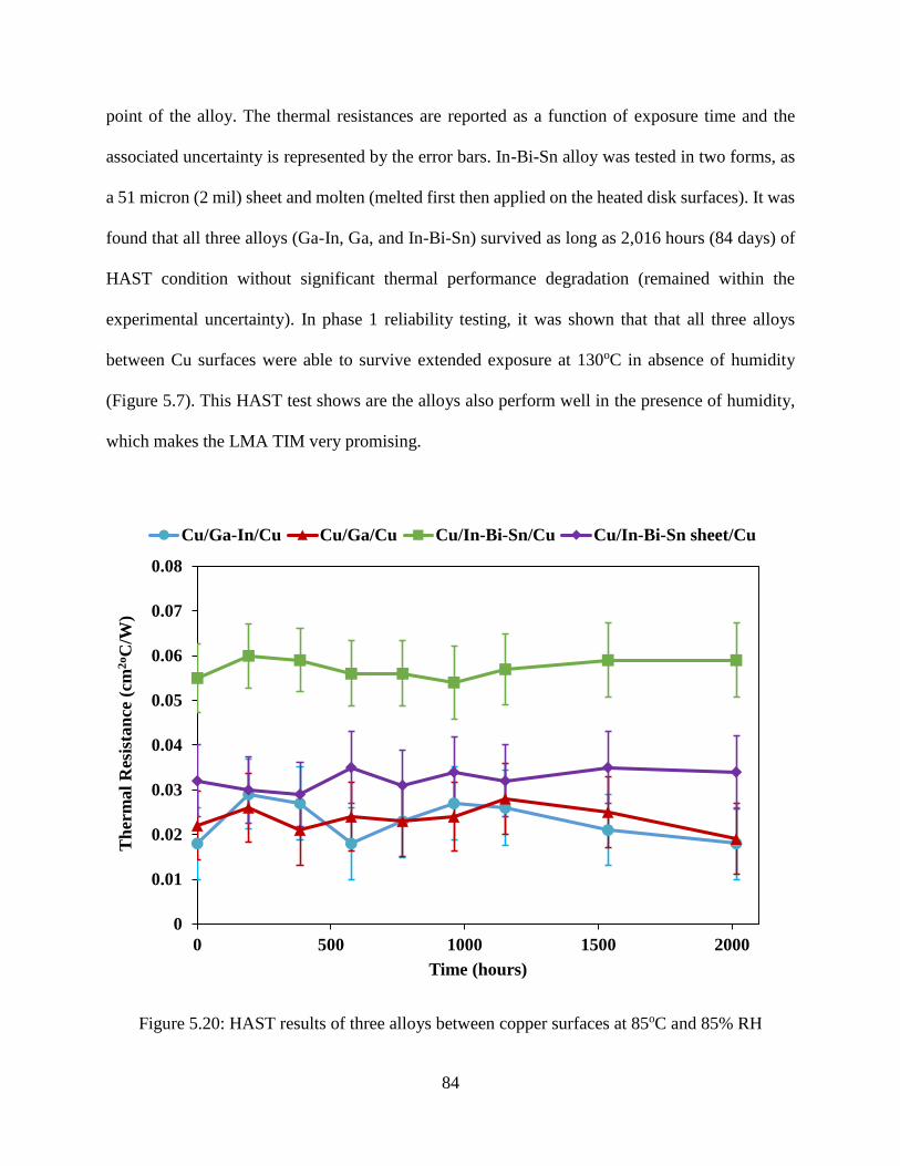
84
point of the alloy. The thermal resistances are reported as a function of exposure time and the
associated uncertainty is represented by the error bars. In-Bi-Sn alloy was tested in two forms, as
a 51 micron (2 mil) sheet and molten (melted first then applied on the heated disk surfaces). It was
found that all three alloys (Ga-In, Ga, and In-Bi-Sn) survived as long as 2,016 hours (84 days) of
HAST condition without significant thermal performance degradation (remained within the
experimental uncertainty). In phase 1 reliability testing, it was shown that that all three alloys
between Cu surfaces were able to survive extended exposure at 130oC in absence of humidity
(Figure 5.7). This HAST test shows are the alloys also perform well in the presence of humidity,
which makes the LMA TIM very promising.
Figure 5.20: HAST results of three alloys between copper surfaces at 85oC and 85% RH
0
0.01
0.02
0.03
0.04
0.05
0.06
0.07
0.08
0 500 1000 1500 2000
Th
erm
al
Res
ista
nce
(cm
2oC
/W)
Time (hours)
Cu/Ga-In/Cu Cu/Ga/Cu Cu/In-Bi-Sn/Cu Cu/In-Bi-Sn sheet/Cu

85
5.8.2 Thermal cycling (-40oC to +125oC)
The third phase thermal cycling test was carried out from -40oC to 125oC. The samples
were heated and cooled at the rate of 3.67oC/min and soaked for 15 minutes at the two extreme
temperatures, ensuring that the interface reached the chamber temperature. The time needed to
complete a thermal cycle was 2 hours.
Thermal cycling results of Ga-In, Ga, and In-Bi-Sn (two forms, molten and 51micron
sheet) alloys between copper surfaces are presented in Figure 5.21 below. It is apparent from the
figure that Ga-In and Ga alloys survived 500 cycles (1000 hours) without significant increase in
thermal resistance. However, for In-Bi-Sn alloy, the thermal resistance increased by about 190 %
when applied as 51 micron sheet. In phase one testing (Figure 5.11), it was found that the thermal
resistance of 102 micron (4 mil) sheet of In-Bi-Sn alloy increased by about 103% after 500 cycles
from -40oC to +80oC. However, due to increase in cycling range (+80oC to +125oC), the
degradation is higher (190%) in the current study after the same number of cycles (500). It can be
noticed that In-Bi-Sn alloy (in both forms) performed well in response to HAST (Figure 5.20),
however, in cycling, performance is degrading with the number of cycles. This is because during
cycling the sample experiences expansion and contraction due to heating and cooling of the joint
in contrast to HAST where the sample is kept at constant temperature. The expansion and
contraction may cause the extrusion of alloy from the interface and thereby create voids at the
interface, which in turn increases the thermal resistance.
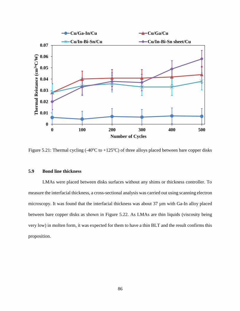
86
Figure 5.21: Thermal cycling (-40oC to +125oC) of three alloys placed between bare copper disks
5.9 Bond line thickness
LMAs were placed between disks surfaces without any shims or thickness controller. To
measure the interfacial thickness, a cross-sectional analysis was carried out using scanning electron
microscopy. It was found that the interfacial thickness was about 37 µm with Ga-In alloy placed
between bare copper disks as shown in Figure 5.22. As LMAs are thin liquids (viscosity being
very low) in molten form, it was expected for them to have a thin BLT and the result confirms this
proposition.
0
0.01
0.02
0.03
0.04
0.05
0.06
0.07
0 100 200 300 400 500
Th
erm
al
Rei
stan
ce (
cm2
oC
/W)
Number of Cycles
Cu/Ga-In/Cu Cu/Ga/Cu
Cu/In-Bi-Sn/Cu Cu/In-Bi-Sn sheet/Cu

87
Figure 5.22: SEM cross-sectional image of Ga-In alloy placed between bare copper disks without
any shims or thickness controller [54]
5.10 Issues with LMAs
5.10.1 LMA Containment
Confinement is a significant challenge when working with LMAs as TIMs. Since LMAs
are a thin (non-viscous) liquid in molten form, it was found that the excess material extruded out
from the interface after melting even at the slightest pressure (<0.5 psi). For example, when a 102
micron thick sheet of In-Bi-Sn alloy was placed between copper disks, it was found that upon
melting almost 70-80% of the alloy came out of the interface as shown in Figure 5.23a below. This
kind of escaping of molten metal from the interface is unwanted and might be detrimental to the
system due to the fact that the electrically conductive molten metal can cause short circuits in
actual electronics cooling application. The alloy extrusion can be greatly reduced by improving
the wetting of the alloy with the mating surfaces which is simply achieved by gently rubbing the
molten alloy on the surfaces. For example, when In-Bi-Sn alloy was placed in its molten form
copper
substrate
Interfacial alloy 37 µm
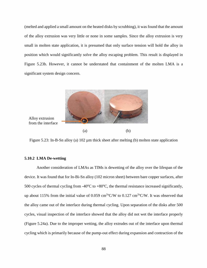
88
(melted and applied a small amount on the heated disks by scrubbing), it was found that the amount
of the alloy extrusion was very little or none in some samples. Since the alloy extrusion is very
small in molten state application, it is presumed that only surface tension will hold the alloy in
position which would significantly solve the alloy escaping problem. This result is displayed in
Figure 5.23b. However, it cannot be understated that containment of the molten LMA is a
significant system design concern.
(a) (b)
Figure 5.23: In-B-Sn alloy (a) 102 µm thick sheet after melting (b) molten state application
5.10.2 LMA De-wetting
Another consideration of LMAs as TIMs is dewetting of the alloy over the lifespan of the
device. It was found that for In-Bi-Sn alloy (102 micron sheet) between bare copper surfaces, after
500 cycles of thermal cycling from -40oC to +80oC, the thermal resistance increased significantly,
up about 115% from the initial value of 0.059 cm2oC/W to 0.127 cm2oC/W. It was observed that
the alloy came out of the interface during thermal cycling. Upon separation of the disks after 500
cycles, visual inspection of the interface showed that the alloy did not wet the interface properly
(Figure 5.24a). Due to the improper wetting, the alloy extrudes out of the interface upon thermal
cycling which is primarily because of the pump-out effect during expansion and contraction of the
Alloy extrusion
from the interface
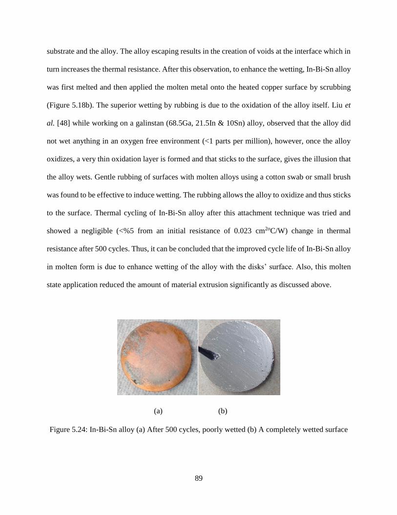
89
substrate and the alloy. The alloy escaping results in the creation of voids at the interface which in
turn increases the thermal resistance. After this observation, to enhance the wetting, In-Bi-Sn alloy
was first melted and then applied the molten metal onto the heated copper surface by scrubbing
(Figure 5.18b). The superior wetting by rubbing is due to the oxidation of the alloy itself. Liu et
al. [48] while working on a galinstan (68.5Ga, 21.5In & 10Sn) alloy, observed that the alloy did
not wet anything in an oxygen free environment (<1 parts per million), however, once the alloy
oxidizes, a very thin oxidation layer is formed and that sticks to the surface, gives the illusion that
the alloy wets. Gentle rubbing of surfaces with molten alloys using a cotton swab or small brush
was found to be effective to induce wetting. The rubbing allows the alloy to oxidize and thus sticks
to the surface. Thermal cycling of In-Bi-Sn alloy after this attachment technique was tried and
showed a negligible (<%5 from an initial resistance of 0.023 cm2oC/W) change in thermal
resistance after 500 cycles. Thus, it can be concluded that the improved cycle life of In-Bi-Sn alloy
in molten form is due to enhance wetting of the alloy with the disks’ surface. Also, this molten
state application reduced the amount of material extrusion significantly as discussed above.
(a) (b)
Figure 5.24: In-Bi-Sn alloy (a) After 500 cycles, poorly wetted (b) A completely wetted surface

90
One side wetting
To avoid the extrusion of the molten alloy, the LAMs were applied as little as required to
wet the surfaces. It was found that by wetting only one copper disk surface with pure Ga resulted
in a significant increase in the thermal resistance upon thermal cycling. After 200 cycles from -
40oC to +80oC, the thermal resistance was found to increase by about five times. Upon separation,
it was observed that the alloy did not wet one disk surface as shown in Figure 5.25. This non-
wetting results in a rapid increase in thermal resistance whereas it was shown (Figure 5.12) that
wetting both surfaces with Ga between copper surfaces survived a large number of cycles. Thus,
it is recommended to apply the alloys on both the mating surfaces, otherwise they won’t form a
good thermal joint.
Figure 5.25: Pure Ga between bare copper after 200 cycles, one side wetting
5.11 Cost consideration
From an economical point of view, LMAs are very promising. As LMAs are thin (low
viscosity) liquids in molten form, only a very small amount (6-9 mg/cm2) is required to wet the
mating surfaces. For example, one gram of pure Ga costs only about $7 and with that it was
possible to prepare at least seven samples (two copper disk of 8.55 cm2 each), which means that
Complete
wetting
Incomplete
wetting
Copper
surface Alloy

91
the LMA interface costs about $1 in the present case. This makes LMAs very cost competitive
compared to many commercial TIMs.

92
Chapter 6 : Summary and Conclusions
Performance of TIMs play a crucial role in the thermal management of microelectronics.
This study investigates the performance of commercial TIMs such as thermal grease, phase change
material, thermal gel and thermal pad as well as low melt alloy as an emerging TIM. Three lead
and cadmium free alloys (In-Bi-Sn, Ga, and Ga-In) with different melting points and various
compositions were chosen to test the thermal performance. The thermal resistance was measured
using the ASTM D5470 standard methodology with a small modification to avoid surface
contamination and to facilitate reliability testing. The bare copper substrates were coated with
nickel and tungsten to investigate different substrate-alloy interactions. To examine the long-term
stability of LMA TIMs, reliability tests were carried out. Reliability tests include isothermal aging
at 130oC and thermal cycling from -40oC to +80oC and -40oC to +125oC and HAST (85oC and
85% RH).
In-situ thermal resistance measurement at 138 kPa showed that the thermal resistance of
LMAs can be as low as 0.005 cm2°C/W and as high as 0.065 cm2°C/W depending on the specimen
preparation. In-situ test was carried out at different pressures from 34.5-345 kPa and results
showed that the thermal resistance of LMAs was invariant with applied pressure in this range,
which indicates an excellent thermal joint even at a lower pressure. Tests were also carried out at
different interface temperatures keeping the pressure constant at 69 kPa (10 psi).
93
Results showed that the thermal resistances of the LMA joints tested were not sensitive to
the interfacial temperature. From this measurements, it can be concluded that once the alloy melts
and seats at the interface, the temperature will not affect the thermal performance. Phase 1
reliability tests showed that all three the alloys between bare copper surface were able to endure
as long as 2,300 hours of aging at 130oC and 2,800 hours of cycling (1,400 cycles) without
deteriorating the thermal performance considerably. Ga and Ga-In alloy between nickel surfaces
survived high temperature aging for longer duration (Figure 5.8), however, failed in thermal
cycling (Figure 5.16). All three alloys between tungsten surfaces could not endure isothermal aging
(Figure 5.9) as well as cycling (Figure 5.17), thermal resistance increased significantly upon these
reliability testing, which indicates an inefficient thermal joint. Results suggests that the diffusion
barrier layer does not help in improving the thermal performance of alloys. In addition, substrate-
alloy interactions (which is primarily diffusion and interfacial reaction) makes the thermal joint
more reliable.
In phase 2 testing, when the alloys were placed between different surfaces (copper and
nickel), all the alloys survived high temperature aging at 130oC for 3,000 hours (Figure 5.18) and
thermal cycling from -40oC TO +80oC for 1,500 cycles (3,000 hours) (Figure 5.19) without
significant thermal performance degradation, which indicates the reliability of alloys at the
interface between dissimilar materials. Phase 3 reliability tests include highly accelerated stress
testing, HAST at 85oC and 85% RH and thermal cycling from -40oC to +125oC of alloys between
bare copper surfaces. HAST tests showed that the alloys were able to withstand as long as 2,016
hours (84 days) without significant increase in thermal resistance, which ensures the stability of
the LMAs at a high humidity and hot environment. Thermal cycling tests also showed that the

94
alloys are capable of surviving large number of cycles. All these reliability tests confirm the
stability of LMAs as TIMs in a harsh environment.
In conclusion, LMAs are environment and health-friendly unless they contain any mercury,
lead or cadmium. In addition, they are easy to apply and commercially available thus
manufacturing at high volume would not be an issue. Many widely used commercial TIMs are
greases or highly solid-loaded pastes that have a high viscosity and in some cases shear-harden,
which makes these types of TIMs more difficult to apply. LMAs are not only more compliant and
less viscous but do not shear-harden. Furthermore, LMAs are cost-effective compared to other
TIMs. As LMAs are thin liquids in molten form, only a very small amount (6-9 mg/cm2) is required
to wet the mating surfaces, which makes an LMA interface at least 25% cheaper compared to
commercial high viscosity greases. However, care must be taken when LMAs are applied at the
interface. By choosing a proper substrate-alloy combination, the LMA interface can be made
highly reliable.
6.1 Future works
In this work, LMAs are found to be effective when applied between the bare copper and
copper-nickel interfaces. In actual processor-heat sink application, the LMAs are usually placed
between the die/chip (which is usually made of silicon) and heat sink (which is usually made of
copper). Even though it is presumed that LMAs will continue to perform reliably between
dissimilar material joints, however, further tests are required to investigate the performance of
LMA as TIMs in actual application. Based on the observation, scope for the future work and
directions are suggested
In-situ thermal performance of LMAs in actual processor-heat sink application.

95
Reliability testing (high temperature aging, thermal cycling, exposure to humidity) of
LMAs at the processor-heat sink interface.
Identify the intermetallic compounds that form at the interface by scanning electron
microscopy or x-ray diffraction techniques.

96
Bibliography
[1] Prasher, Ravi. "Thermal interface materials: historical perspective, status, and future
directions." Proceedings of the IEEE 94.8 (2006): 1571-1586.
[2] Gwinn, Joshua P., and R. L. Webb. "Performance and testing of thermal interface
materials." Microelectronics Journal 34.3 (2003): 215-222
[3] Frank P. Incropera, David P. Dewitt, Theodore L. Bergman, and Adrienne S. Lavine.
.Fundamentals of heat and mass transfer. 6th edition, John Wiley & Sons, 2007.
[4] Martin, Y., and Kessel, T.V. "High performance Liquid Metal Thermal Interface for Large
Volume Production." IMAPS Thermal and Power Management, San Jose CA (2007).
[5] Pfahl, Bob, Haley Fu, and Chuck Richardson. "Highlights of iNEMI 2013 technology
roadmaps." Electronic Manufacturing Technology Symposium (IEMT), 2012 35th
IEEE/CPMT International. IEEE, 2012.
[6] Mahajan, R., Nair, R., Wakharkar, V., Swan, J., Tang, J., and Vandentop, G. "Emerging
Drirections for Packaging Technologies." Intel Technology Journal 6.2 (2002): 62-75.
[7] Wasniewski, Joseph R., David H. Altman, Stephen L. Hodson, Timothy S. Fisher, Anuradha
Bulusu, Samuel Graham, and Baratunde A. Cola. "Characterization of metallically bonded
carbon nanotube-based thermal interface materials using a high accuracy 1D steady-state
technique." Journal of Electronic Packaging 134.2 (2012): 020901.
97
[8] Roy, Chandan K., Sushil Bhavnani, Michael C. Hamilton, R. Wayne Johnson, Jonathan L.
Nguyen, Roy W. Knight, and Daniel K. Harris."Investigation into the application of low
melting temperature alloys as wet thermal interface materials." International Journal of Heat
and Mass Transfer 85 (2015): 996-1002.
[9] Chung, D. D. L. "Materials for thermal conduction." Applied Thermal Engineering 21.16
(2001): 1593-1605.
[10] Rauch, Bob. "Understanding the performance characteristics of phase-change thermal
interface materials." Thermal and Thermomechanical Phenomena in Electronic Systems,
2000. ITHERM 2000. The Seventh Intersociety Conference on. Vol. 1. IEEE, 2000.
[11] Blazej, D. "Thermal Interface Materials." Electronics Cooling. 9.4 (2003): 14-20.
[12] Roy, Chandan K., Sushil Bhavnani, Mike Hamilton, Wayne R. Johnson, Roy W. Knight, and
Daniel K. Harris."Performance of Low Melt Alloys as Thermal Interface Materials." 31st
Semiconductor Thermal Measurement and Management Symposium (SEMI-THERM) 2015,
IEEE, 2015
[13] Roy, Chandan K., Sushil Bhavnani, Mike Hamilton, Wayne R. Johnson, Roy W. Knight, and
Daniel K. Harris. "Application of Low Melt Alloys as Compliant Thermal Interface Materials:
A Study of Performance and Degradation under Thermal Duress." Electronics Cooling. June,
2015: 26-31
[14] Prasher, Ravi S., and James C. Matayabas Jr. "Thermal contact resistance of cured gel
polymeric thermal interface material." Components and Packaging Technologies, IEEE
Transactions on 27.4 (2004): 702-709.
[15] Samson E., Sridhar V. Machiroutu, Je-Young Chang, Ishmael Santos, Jim Hermerding, Ashay
Dani, Ravi Prasher, and David W. Song. "Some thermal technology and thermal management
98
considerations in the design of next generation Intel Centrino Mobile Technology platforms."
Intel Technology Journal 9.1, 2005.
[16] Sarvar, Farhad, David C. Whalley, and Paul P. Conway. "Thermal interface materials-A review
of the state of the art." Electronics Systemintegration Technology Conference, 2006. 1st. Vol.
2. IEEE, 2006.
[17] Xu, Jun, and Timothy S. Fisher. "Enhancement of thermal interface materials with carbon
nanotube arrays." International Journal of Heat and Mass Transfer49.9 (2006): 1658-1666.
[18] Cross, Robert, Baratunde A. Cola, Timothy Fisher, Xianfan Xu, Ken Gall, and Samuel
Graham. "A metallization and bonding approach for high performance carbon nanotube
thermal interface materials." Nanotechnology21.44 (2010): 445705.
[19] Tong, Tao, Yang Zhao, Lance Delzeit, Ali Kashani, M. Meyyappan, and Arun Majumdar.
"Dense vertically aligned multiwalled carbon nanotube arrays as thermal interface
materials." Components and Packaging Technologies, IEEE Transactions on 30.1 (2007): 92-
100.
[20] Hu, Xuejiao, Linan Jiang, and Kenneth E. Goodson. "Thermal conductance enhancement of
particle-filled thermal interface materials using carbon nanotube inclusions." Thermal and
Thermomechanical Phenomena in Electronic Systems, 2004. ITHERM'04. The Ninth
Intersociety Conference on. IEEE, 2004.
[21] Choi, S. U. S., Z. G. Zhang, Wu Yu, F. E. Lockwood, and E. A. Grulke. "Anomalous thermal
conductivity enhancement in nanotube suspensions." Applied physics letters 79.14 (2001):
2252-2254.
99
[22] Fabris, Drazen, Michael Rosshirt, Christopher Cardenas, Patrick Wilhite, Toshishige Yamada,
and Cary Y. Yang. "Application of carbon nanotubes to thermal interface materials." Journal
of Electronic Packaging 133.2 (2011): 020902.
[23] Nan, Ce-Wen, Gang Liu, Yuanhua Lin, and Ming Li. "Interface effect on thermal conductivity
of carbon nanotube composites." Applied Physics Letters 85.16 (2004): 3549-3551.
[24] Goyal, Vivek, and Alexander A. Balandin. "Thermal properties of the hybrid graphene-metal
nano-micro-composites: applications in thermal interface materials." Applied Physics
Letters 100.7 (2012): 073113.
[25] Shahil, Khan MF, and Alexander A. Balandin. "Graphene–multilayer graphene
nanocomposites as highly efficient thermal interface materials." Nano letters12.2 (2012): 861-
867.
[26] Berber, Savas, Young-Kyun Kwon, and David Tománek. "Unusually high thermal
conductivity of carbon nanotubes." Physical review letters 84.20 (2000): 4613.
[27] Zhu, Lingbo, Dennis W. Hess, and C. P. Wong. "Assembling carbon nanotube films as thermal
interface materials." Electronic Components and Technology Conference, 2007. ECTC'07.
Proceedings. 57th. IEEE, 2007.
[28] Barako, Michael T., Yuan Gao, Amy M. Marconnet, Mehdi Asheghi, and Kenneth E.
Goodson. "Solder-bonded carbon nanotube thermal interface materials." Thermal and
Thermomechanical Phenomena in Electronic Systems (ITherm), 2012 13th IEEE Intersociety
Conference on. IEEE, 2012.
[29] Peacock, Melissa A., Chandan K. Roy, Michael C. Hamilton, R. Wayne Johnson, Roy W.
Knight, and Daniel K. Harris. "Characterization of transferred vertically aligned carbon
100
nanotubes arrays as thermal interface materials." International Journal of Heat and Mass
Transfer 97 (2016): 94-100.
[30] Hone, J., M. C. Llaguno, M. J. Biercuk, A. T. Johnson, B. Batlogg, Z. Benes, and J. E.
Fischer."Thermal properties of carbon nanotubes and nanotube-based materials." Applied
Physics A 74.3 (2002): 339-343.
[31] Cook, R. S., K. H. Token, and R. L. Calkins. "A novel concept for reducing thermal contact
resistance." Journal of Spacecraft and Rockets 21.1 (1984): 122-124.
[32] Webb, Ralph L., and Joshua P. Gwinn. "Low melting point thermal interface
material." Thermal and Thermomechanical Phenomena in Electronic Systems, 2002. ITHERM
2002. The Eighth Intersociety Conference on. IEEE, 2002.
[33] Macris, Chris G., Thomas R. Sanderson, Robert G. Ebel, Christopher B. Leyerle, and Enerdyne
Solutions. "Performance, reliability, and approaches using a low melt alloy as a thermal
interface material." Proceedings IMAPS. 2004.
[34] Hill, Richard F., and Jason L. Strader. "Practical utilization of low melting alloy thermal
interface materials." Semiconductor Thermal Measurement and Management Symposium,
2006 IEEE Twenty-Second Annual IEEE. IEEE, 2006.
[35] Carlberg, Björn, Teng Wang, Yifeng Fu, Johan Liu, and Dongkai Shangguan."Nanostructured
polymer-metal composite for thermal interface material applications." Electronic Components
and Technology Conference, 2008. ECTC 2008. 58th. IEEE, 2008.
[36] Hamdan, A., A. McLanahan, R. Richards, and C. Richards. "Characterization of a liquid–metal
microdroplet thermal interface material." Experimental Thermal and Fluid Science 35.7
(2011): 1250-1254
101
[37] Yang, E., Hongyan Guo, Jingdong Guo, Jianku Shang, and Mingguang Wang. "Thermal
Performance of Low-Melting-Temperature Alloy Thermal Interface Materials." Acta
Metallurgica Sinica (English Letters) 27.2 (2014): 290-294.
[38] Shaddock, David, Stanton Weaver, Ioannis Chasiotis, Binoy Shah, and Dalong
Zhong. "Development of a compliant nanothermal interface material." ASME 2011 Pacific
Rim Technical Conference and Exhibition on Packaging and Integration of Electronic and
Photonic Systems. American Society of Mechanical Engineers, 2011.
[39] Luo, Xin, Yong Zhang, Carl Zandén, Murali Murugesan, Yu Cao, Lilei Ye, and Johan Liu.
"Novel thermal interface materials: boron nitride nanofiber and indium composites for
electronics heat dissipation applications." Journal of Materials Science: Materials in
Electronics 25.5 (2014): 2333-2338.
[40] Wikipedia contributors. "Kopp's law." Wikipedia, The Free Encyclopedia, 22 Nov. 2015. Web.
6 Apr. 2016.
[41] "TCi Thermal Conductivity Analyzer." How It Works. C-Therm. Web. 06 Apr. 2016.
[42] Sofia, John W. "Analysis of thermal transient data with synthesized dynamic models for
semiconductor devices." Components, Packaging, and Manufacturing Technology, Part A,
IEEE Transactions on 18.1 (1995): 39-47.
[43] Cola, Baratunde A., Jun Xu, Changrui Cheng, Xianfan Xu, Timothy S. Fisher, and Hanping
Hu. "Photoacoustic characterization of carbon nanotube array thermal interfaces." Journal of
applied physics 101.5 (2007): 054313.
[44] McNamara, Andrew J., Yogendra Joshi, and Zhuomin M. Zhang. "Characterization of
nanostructured thermal interface materials–a review."International Journal of Thermal
Sciences 62 (2012): 2-11.
102
[45] Kohli, Punit, Martin Sobczak, Jeff Bowin, and Michael Matthews. "Advanced thermal
interface materials for enhanced flip chip BGA." Electronic Components and Technology
Conference, 2001. Proceedings., 51st. IEEE, 2001.
[46] ASTM standard D5470, 2012,” Standard Test Method for Thermal Transmission Properties of
Thermally Conductive Electrical Insulation Materials”, ASTM international, West
Conshohocken, PA, 2012, DOI: 10.1520/D5470-12, www.astm.org .
[47] Analysis Tech. Material Thermal Testers: TIM Tester 1400 Specifications. 2012. 18 April
2014.
[48] Liu, Tingyi, Prosenjit Sen, and Chang-Jin Kim. "Characterization of nontoxic liquid-metal
alloy galinstan for applications in microdevices."Microelectromechanical Systems, Journal
of 21.2 (2012): 443-450.
[49] DeVoto, Douglas, Paul Paret, Mark Mihalic, Sreekant Narumanchi, Avram Bar-Cohen, and
Kaiser Matin. "Thermal performance and reliability characterization of bonded interface
materials (BIMs)." Thermal and Thermomechanical Phenomena in Electronic Systems
(ITherm), 2014 IEEE Intersociety Conference on. IEEE, 2014.
[50] Kim, Dae-Gon, Jeong-Won Yoon, Chang-Youl Lee, and Seung-Boo Jung. "Reaction
Diffusion and Formation of Cu11In9 and In27Ni10 Phases in the Couple of Indium-
Substrates." Materials Transactions 44.1 (2003): 72-77.
[51] Roy, Chandan K., Sushil Bhavnani, Michael C. Hamilton, R. Wayne Johnson, Roy W. Knight,
and Daniel K. Harris. "Accelerated aging and thermal cycling of low melting temperature
alloys as wet thermal interface materials." Microelectronics Reliability 55.12 (2015): 2698-
2704.
103
[52] Ancharov, A. I., T. F. Grigoryeva, A. P. Barinova, and V. V. Boldyrev. "Interaction between
copper and gallium." Russian Metallurgy (Metally) 2008.6 (2008): 475-479.
[53] Schmetterer, Clemens, Hans Flandorfer, Christian L. Lengauer, Jean-Pierre Bros, and Herbert
Ipser. "The system Ga–Ni: A new investigation of the Ga-rich part." Intermetallics 18.2
(2010): 277-285.
[54] Roy, Chandan K., Sushil Bhavnani, Michael C. Hamilton, R. Wayne Johnson, Roy W. Knight,
and Daniel K. Harris "Durability of low melt alloys as thermal interface materials." J. Electron.
Packag 138.1 (2016): doi: 10.1115/1.4032462.
[55] Roy, Chandan K., Sushil Bhavnani, Michael C. Hamilton, R. Wayne Johnson, Roy W. Knight,
and Daniel K. Harris "Thermal performance of low melting temperature alloys at the interface
between dissimilar materials." Applied Thermal Engineering 99 (2016): 72-79

104
Appendix
Simulation data for calculation of Probe disturbance
Probe
angle
(Degree)
Probe location
l (mm)
TIM top surface
Tmax (oC)
TIM top surface
Tmin (oC)
ΔTupper
(Tmax-Tmin)
(oC)
ΔTTIM
(oC)
Disturbance
ΔTupper/ ΔTTIM
(%)
0
0.8 27.0157 26.9142 0.1015 0.2322 43.71
1.6 27.0198 26.9806 0.0392 0.2321 16.89
2.4 26.9732 26.9381 0.0351 0.2313 15.17
90
0.8 27.2242 26.696 0.5282 0.2325 227.18
1.6 27.271 27.0065 0.2645 0.2358 112.17
2.4 27.0216 26.8521 0.1695 0.2309 73.41
180
0.8 27.2098 26.6843 0.5255 0.2322 226.31
1.6 27.0971 26.8393 0.2578 0.2319 111.17
2.4 27.0352 26.8596 0.1756 0.2313 75.92
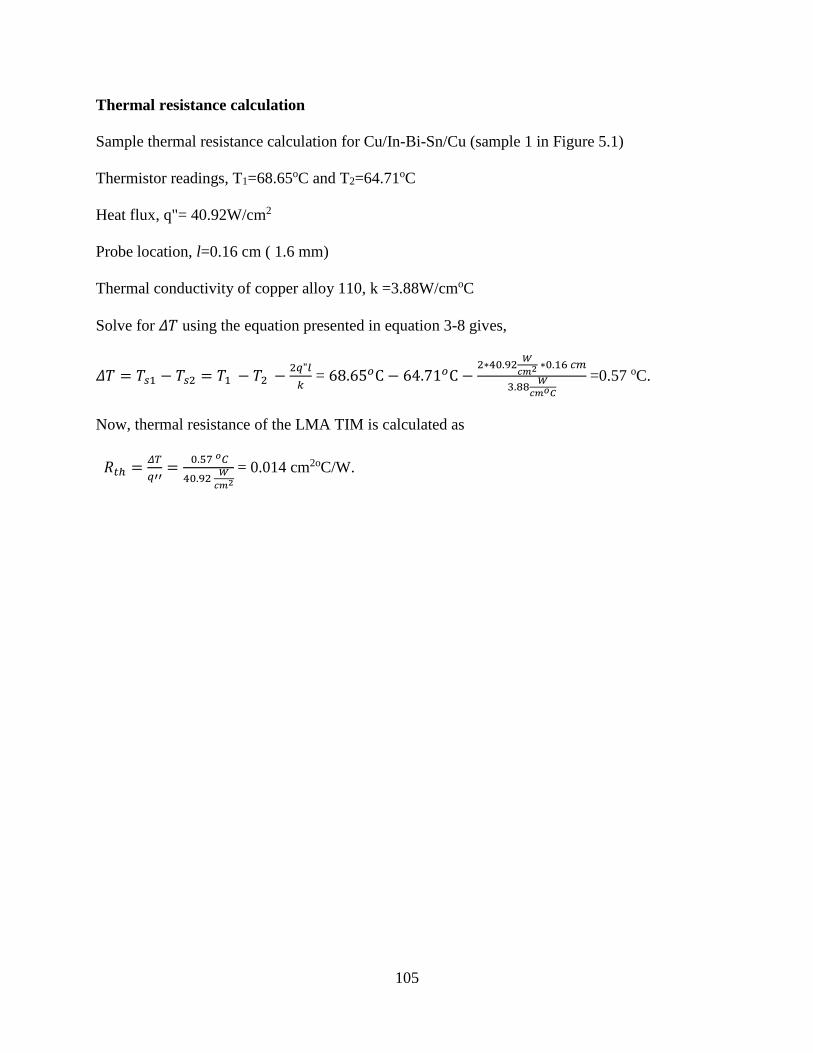
105
Thermal resistance calculation
Sample thermal resistance calculation for Cu/In-Bi-Sn/Cu (sample 1 in Figure 5.1)
Thermistor readings, T1=68.65oC and T2=64.71oC
Heat flux, q"= 40.92W/cm2
Probe location, l=0.16 cm ( 1.6 mm)
Thermal conductivity of copper alloy 110, k =3.88W/cmoC
Solve for 𝛥𝑇 using the equation presented in equation 3-8 gives,
𝛥𝑇 = 𝑇𝑠1 − 𝑇𝑠2 = 𝑇1 − 𝑇2 −2𝑞"𝑙
𝑘 = 68.65𝑜C − 64.71𝑜C −
2∗40.92𝑊
𝑐𝑚2 ∗0.16 𝑐𝑚
3.88𝑊
𝑐𝑚𝑜𝐶
=0.57 oC.
Now, thermal resistance of the LMA TIM is calculated as
𝑅𝑡ℎ =𝛥𝑇
𝑞′′=
0.57 𝑜𝐶
40.92 𝑊
𝑐𝑚2
= 0.014 cm2oC/W.