application note no. 067 - infineon
TRANSCRIPT

Appl icat ion Note No. 067General Purpose Wide Band Dr iver Ampl i f ier using BGA614
Appl icat ion Note, Rev. 2.0, Dec. 2007
RF & Protect ion Devices

Edition 2007-01-04Published byInfineon Technologies AG81726 München, Germany© Infineon Technologies AG 2009.All Rights Reserved.
LEGAL DISCLAIMERTHE INFORMATION GIVEN IN THIS APPLICATION NOTE IS GIVEN AS A HINT FOR THE IMPLEMENTATION OF THE INFINEON TECHNOLOGIES COMPONENT ONLY AND SHALL NOT BE REGARDED AS ANY DESCRIPTION OR WARRANTY OF A CERTAIN FUNCTIONALITY, CONDITION OR QUALITY OF THE INFINEON TECHNOLOGIES COMPONENT. THE RECIPIENT OF THIS APPLICATION NOTE MUST VERIFY ANY FUNCTION DESCRIBED HEREIN IN THE REAL APPLICATION. INFINEON TECHNOLOGIES HEREBY DISCLAIMS ANY AND ALL WARRANTIES AND LIABILITIES OF ANY KIND (INCLUDING WITHOUT LIMITATION WARRANTIES OF NON-INFRINGEMENT OF INTELLECTUAL PROPERTY RIGHTS OF ANY THIRD PARTY) WITH RESPECT TO ANY AND ALL INFORMATION GIVEN IN THIS APPLICATION NOTE.
InformationFor further information on technology, delivery terms and conditions and prices please contact your nearest Infineon Technologies Office (www.infineon.com).
WarningsDue to technical requirements components may contain dangerous substances. For information on the types in question please contact your nearest Infineon Technologies Office.Infineon Technologies Components may only be used in life-support devices or systems with the express written approval of Infineon Technologies, if a failure of such components can reasonably be expected to cause the failure of that life-support device or system, or to affect the safety or effectiveness of that device or system. Life support devices or systems are intended to be implanted in the human body, or to support and/or maintain and sustain and/or protect human life. If they fail, it is reasonable to assume that the health of the user or other persons may be endangered.

Application Note No. 067
Application Note 3 Rev. 2.0, 2007-01-04
TrademarksSIEGET® is a registered trademark of Infineon Technologies AG.
Application Note No. 067
Revision History: 2007-01-04, Rev. 2.0Previous Version: 2000-02-03Page Subjects (major changes since last revision)All Document layout change
Application Note 4 Rev. 2.0, 2007-01-04
Application Note No. 067
General Purpose Wide Band Driver Amplifier using BGA614
1 General Purpose Wide Band Driver Amplifier using BGA614Features
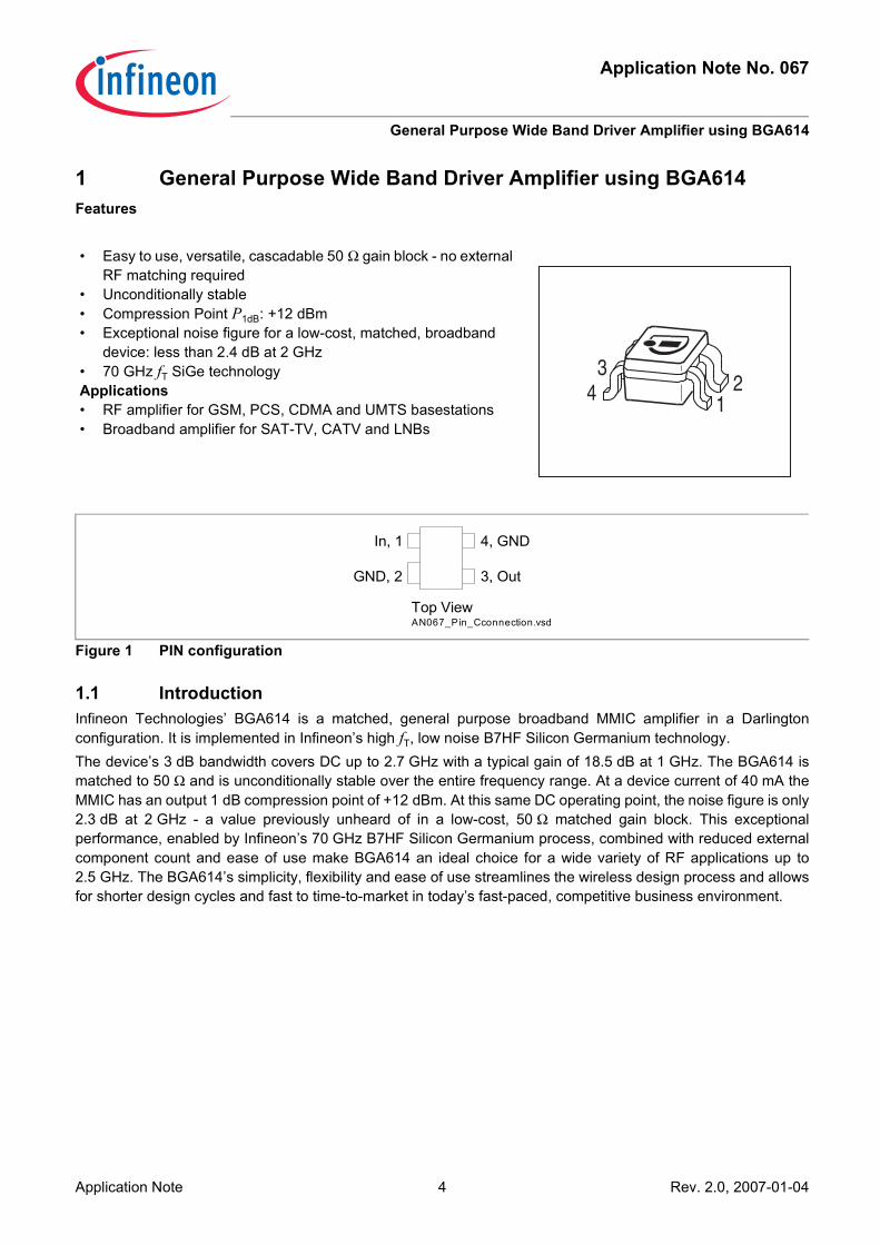
Figure 1 PIN configuration
1.1 IntroductionInfineon Technologies’ BGA614 is a matched, general purpose broadband MMIC amplifier in a Darlingtonconfiguration. It is implemented in Infineon’s high fT, low noise B7HF Silicon Germanium technology.The device’s 3 dB bandwidth covers DC up to 2.7 GHz with a typical gain of 18.5 dB at 1 GHz. The BGA614 ismatched to 50 Ω and is unconditionally stable over the entire frequency range. At a device current of 40 mA theMMIC has an output 1 dB compression point of +12 dBm. At this same DC operating point, the noise figure is only2.3 dB at 2 GHz - a value previously unheard of in a low-cost, 50 Ω matched gain block. This exceptionalperformance, enabled by Infineon’s 70 GHz B7HF Silicon Germanium process, combined with reduced externalcomponent count and ease of use make BGA614 an ideal choice for a wide variety of RF applications up to2.5 GHz. The BGA614’s simplicity, flexibility and ease of use streamlines the wireless design process and allowsfor shorter design cycles and fast to time-to-market in today’s fast-paced, competitive business environment.
• Easy to use, versatile, cascadable 50 Ω gain block - no external RF matching required
• Unconditionally stable• Compression Point P1dB: +12 dBm• Exceptional noise figure for a low-cost, matched, broadband
device: less than 2.4 dB at 2 GHz• 70 GHz fT SiGe technologyApplications• RF amplifier for GSM, PCS, CDMA and UMTS basestations• Broadband amplifier for SAT-TV, CATV and LNBs
12
34
AN067_Pin_Cconnection.vsd
In, 1 4, GND
Top View
GND, 2 3, Out

Application Note No. 067
General Purpose Wide Band Driver Amplifier using BGA614
Application Note 5 Rev. 2.0, 2007-01-04
Figure 2 Equivalent Circuit of BGA614
Figure 3 Schematic Diagram
Table 1 Bill of MaterialsName Value Unit Size Manufacturer FunctionC1 100 pF 0402 Various DC blockC2 100 pF 0402 Various DC blockC3 100 pF 0402 Various RF bypassL1 47 nH 0402 Toko LL 1005-FH RF blockR1 62 Ω 0402 Various BiasingIC1 BGA614 SOT343 Infineon Technologies SiGe MMIC
AN067_equivalent_circuit.vsd
In
Out
GND
AN067_schematic.vsd
Vcc
C1100pF
C2100pF
C3100pF
L147nH
R162Ω
1
2 3
4Q1
BGA614
In
Out

Application Note 6 Rev. 2.0, 2007-01-04
Application Note No. 067
General Purpose Wide Band Driver Amplifier using BGA614
Figure 4 PCB Cross Section
1.2 Circuit DesignThis application note describes the design of a general purpose broadband driver amplifier for the frequency bandbetween 1.7 GHz and 2.2 GHz using the BGA614. This band covers the Tx as well as Rx frequencies of variousstandards from GSM1800 or DCS1800, North America PCS band, up to W-CDMA.Implementing an amplifier circuit using BGA614 is a simple, straightforward task. As both input and output arealready matched to 50 Ω and BGA614 is an unconditionally stable device, there is no need to work on the RFportion of the amplifier design, leaving only DC biasing issues to contend with. The broadband 50 Ω match alsoeases and speeds integration of the MMIC with any external filters used.Figure 5 shows the component placement on the application PCB. There are only five external componentsnecessary for the complete amplifier circuit. The low external parts count simplifies manufacturing issues andreduces required PCB area and associated costs.
Table 2 Performance OverviewParameter Value
1.7 GHz 1.95 GHz 2.2 GHzSupply voltage VCC 5 V 5 V 5 VSupply current ID 41.2 mA 41.2 mA 41.2 mAGain 17.0 dB 16.5 dB 15.9 dBNoise figure 2.38 dB 2.35 dB 2.32 dBInput return loss 15.5 dB 14.5 dB 13.7 dBOutput return loss 17.7 dB 16.8 dB 16.0 dBReverse Isolation 21.1 dB 20.9 dB 20.6 dBOutput P1dB 12.6 dBm 12.2 dBm 12.6 dBmOutput IP3
1)
1) ∆f = 1 MHz; -20 dBm per tone23.6 dBm 21.0 dBm 20.8 dBm
AN067_PCB_cross_section.vsd
0.8 mm FR4
0.2 mm FR435 µm Cu
35 µm Cu
35 µm Cu
for mechanicalrigidity of PCB
Application Note No. 067
General Purpose Wide Band Driver Amplifier using BGA614
Application Note 7 Rev. 2.0, 2007-01-04
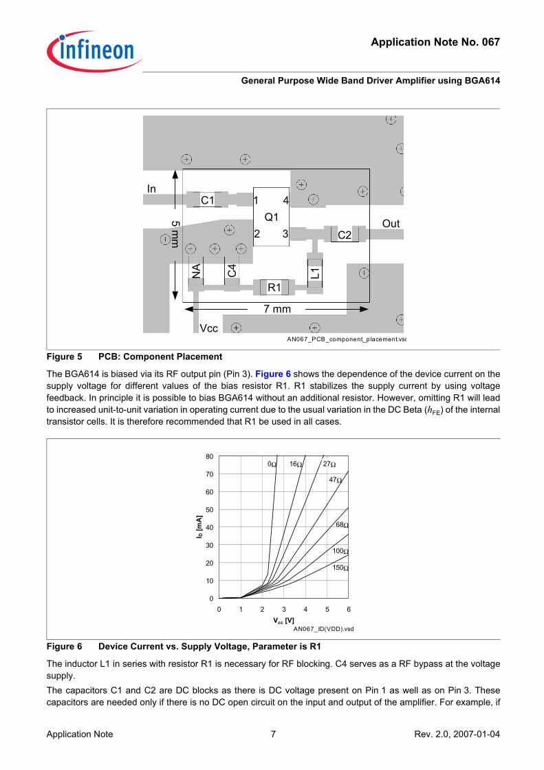
Figure 5 PCB: Component Placement
The BGA614 is biased via its RF output pin (Pin 3). Figure 6 shows the dependence of the device current on thesupply voltage for different values of the bias resistor R1. R1 stabilizes the supply current by using voltagefeedback. In principle it is possible to bias BGA614 without an additional resistor. However, omitting R1 will leadto increased unit-to-unit variation in operating current due to the usual variation in the DC Beta (hFE) of the internaltransistor cells. It is therefore recommended that R1 be used in all cases.
Figure 6 Device Current vs. Supply Voltage, Parameter is R1
The inductor L1 in series with resistor R1 is necessary for RF blocking. C4 serves as a RF bypass at the voltagesupply.The capacitors C1 and C2 are DC blocks as there is DC voltage present on Pin 1 as well as on Pin 3. Thesecapacitors are needed only if there is no DC open circuit on the input and output of the amplifier. For example, if
AN067_PCB_component_placement.vsd
C1
C2C
4
NA
R1
L1
Q1
In
Out
7 mm
5 mm
Vcc
1
2
4
3
0
10
20
30
40
50
60
70
80
0 1 2 3 4 5 6Vcc [V]
I D [m
A]
0Ω 16Ω 27Ω
47Ω
68Ω
100Ω
150Ω
AN067_ID(VDD).vsd

Application Note 8 Rev. 2.0, 2007-01-04
Application Note No. 067
Measurement Results
a filter that presents a DC open circuit is used ahead of or after the BGA614, the corresponding DC blockingcapacitor may be omitted.
1.3 RemarksBGA614 is only one member of Infineon Technologies’ broadband Darlingtion MMIC amplifier family. Thecomplete family consists of BGA612, BGA614 and BGA616 to cover a wide range to typical supply currents.BGA612 is designed for a typical supply current of 20 mA, BGA614 for 40 mA and the BGA616 for 60 mA.The BGA614 application PCB can be used to evaluate BGA612 and BGA616 as well. It is only necessary tochange the value of R1 to adjust the devices’ supply current accordingly. Typical values of R1 are 135 Ω atVCC = 5 V for BGA612 and 33 Ω at VCC = 6 V for BGA616.For further and more detailed dependencies of the devices’ supply currents please refer to the appropriate datasheets where graphs like the one in Figure 6 can be found for BGA612 and BGA616.
2 Measurement Results
Figure 7 Gain
AN067_Gain(f).vsd
12
13
14
15
16
17
18
1,7 1,8 1,9 2 2,1 2,2
Frequency [GHz]
Gai
n [d
B]

Application Note No. 067
Measurement Results
Application Note 9 Rev. 2.0, 2007-01-04
Figure 8 Matching
Figure 9 Noise Figure
AN067_Return_Loss(f).vsd
-20
-18
-16
-14
-12
-10
1,7 1,8 1,9 2 2,1 2,2
Frequency [GHz]
Ret
urn
Loss
[dB
]
s11
s22
AN067_Noise_Figure(f).vsd
1,6
2
2,4
2,8
3,2
3,6
1,7 1,8 1,9 2 2,1 2,2Frequency [GHz]
Noi
se F
igur
e [d
B]

Application Note 10 Rev. 2.0, 2007-01-04
Application Note No. 067
Measurement Results
Figure 10 Reverse Isolation
Figure 11 Stability Factor
AN067_Reverse_Isolation(f).vsd
-25
-23
-21
-19
-17
-15
1,7 1,8 1,9 2 2,1 2,2Frequeny [GHz]
Rev
erse
Isol
atio
n [d
B]
AN067_K_B1(f).vsd
0,2
0,4
0,6
0,8
1
1,2
1,4
1,6
0 1 2 3 4 5 6Frequency [GHz]
K, B
1
K
B1

Application Note No. 067
Measurement Results
Application Note 11 Rev. 2.0, 2007-01-04
Figure 12 Gain Compression
Figure 13 Gain, wide span
AN067_Pout(Pin).vsd
-15
-10
-5
0
5
10
15
-30 -25 -20 -15 -10 -5 0Pin [dBm]
P out
[dB
m]
10
12
14
16
18
20
22
Gai
n [d
B]
Gain
Pout
AN067_wide_span_Gain(f).vsd
8
10
12
14
16
18
20
0 1 2 3 4 5 6Frequency [GHz]
Gai
n [d
B]

Application Note 12 Rev. 2.0, 2007-01-04
Application Note No. 067
Measurement Results
Figure 14 Matching, wide span
AN067_wide_span_Return_loss(f).vsd
-25
-20
-15
-10
-5
0
0 1 2 3 4 5 6Frequency [GHz]
Ret
urn
Loss
[dB
]
s11
s22