application note an-70 linkswitch-tn2 family · 2017-02-01 · application note an-70...
TRANSCRIPT
Application Note AN-70 LinkSwitch-TN2 Family
www.power.com January 2017
Design Guide
IntroductionLinkSwitch™-TN2 ICs combine a high-voltage (725 V) power MOSFET switch with an ON/OFF controller onto a monolithic IC. Jitter is added to the switching frequency to achieve lower EMI and the IC is fully fault protected. Auto-restart limits device and circuit dissipation during overload and output short-circuit while over temperature protection disables the internal power MOSFET during thermal faults. The high thermal shutdown threshold is ideal for applications where the ambient temperature is high while the large hysteresis protects the PCB and surrounding components from high average temperatures.
The LinkSwitch-TN2 family is designed for any application where a non-isolated supply is required such as appliances (coffee machines, rice cookers, dishwashers, microwave ovens etc.), night lights, emergency exit signs and LED drivers. LinkSwitch-TN2 ICs can be configured in all common topologies to give a line or neutral referenced output and an inverted or non-inverted output voltage – ideal for
applications using TRIACs for AC load control. Using a switching power supply rather than a passive dropper (capacitive or resistive) gives a number of advantages, some of which are listed below.
• Universal input – the same power supply/product can be usedworldwide
• High power density – smaller size, typically no X class capacitanceneeded for most designs
• High efficiency – full load efficiencies >75% typical for 12 V output,120 mA
• Excellent line and load regulation• High efficiency at light load – ON/OFF control maintains high
efficiency even at light load• Extremely energy efficient – input power <30 mW at no-load• Entirely manufacturable with SMD components• Fully fault protected (overload, short-circuit and thermal faults)• Scalable – LinkSwitch-TN2 family allows the same basic design to be
used from <50 mA to 360 mA.
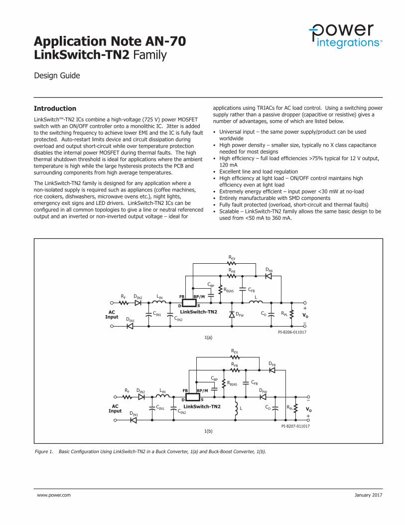
Figure 1. Basic Configuration Using LinkSwitch-TN2 in a Buck Converter, 1(a) and Buck-Boost Converter, 1(b).
1(b)
1(a)
VOAC
Input
PI-8207-011017
+
FB BP/M
SD
LinkSwitch-TN2
RF DIN2 LIN
CBPRBIAS CFB
RFB
REX
L
DFW
CO RPL
DFB
DIN1
CIN1 CIN2
VO
RF DIN2
DIN1
LIN
CIN1CIN2
RFB DFB
RBIAS CFB
CBP
DFW CO RPLAC
Input
PI-8206-011017
+
FB BP/M
SD
REX
LinkSwitch-TN2
L
Rev. A 01/17
2
Application Note AN-70
www.power.com
ScopeThis application note is for designing a non-isolated power supply using the LinkSwitch-TN2 family of devices. This document describes the design procedure for buck and buck-boost converters using the LinkSwitch-TN2 family of integrated off-line switchers. The objective of this document is to provide power supply engineers with guidelines in order to enable them to quickly build efficient and low-cost buck or buck-boost converter based power supplies using low-cost off-the-shelf inductors. Complete design equations are provided for the selection of the converter’s key components. Since the power MOSFET and controller are integrated into a single IC, the design process is greatly simplified, the circuit configuration has few parts and no transformer is required. Therefore a quick start section is provided that allows off-the-shelf components to be selected for typical output voltages and currents. To simplify the task this application note refers directly to the PIXls design spreadsheet that is part of the PI Expert™ design software suite. The basic configuration used in LinkSwitch-TN2 power supplies is shown in Figure 1, which also serves as the reference circuit for component identifications used in the description throughout this application note.
In addition to this application note, the reader may also find the LinkSwitch-TN2 Reference Design Kit (RDK) containing an engineering
prototype board, engineering report and device samples useful as an example of a working power supply. Further details on downloading PI Expert, obtaining a RDK and updates to this document can be found at www.power.com.
Quick StartReaders wanting to start immediately can use the following informa-tion to quickly select the components for a new design, using Figure 1 and Tables 1 and 2 as references.
1. For AC input designs select the input stage (Table 10).2. Select the topology (Tables 1 and 2). If better than ±5% output
regulation is required, then use optocoupler feedback with suitable reference such as TL431 or a precision Zener is required.
3. Select the LinkSwitch-TN2 device, L, RFB or VZ, RBIAS, CFB, RZ and the reverse recovery time for DFW (Table 4: Buck, Table 5: Buck-Boost).
4. Select freewheeling diode to meet tRR determined in Step 3 (table 3).
5. For direct feedback designs, if the minimum load <3 mA then calculate RPL = VO/3 mA.
6. Select CO as 100 mF, 1.25 × VO, low ESR type.7. Construct prototype and verify design.
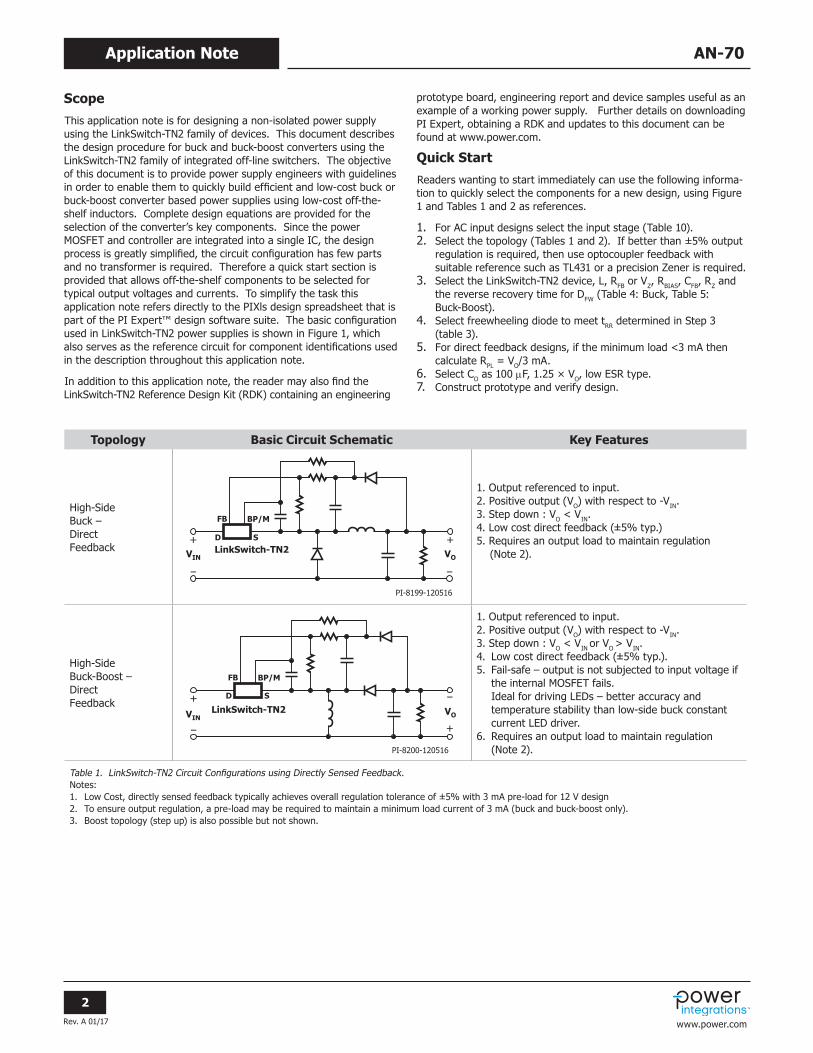
Topology Basic Circuit Schematic Key Features
High-Side Buck – Direct Feedback
1. Output referenced to input. 2. Positive output (VO) with respect to -VIN. 3. Step down : VO < VIN. 4. Low cost direct feedback (±5% typ.)5. Requires an output load to maintain regulation (Note 2).
High-Side Buck-Boost – Direct Feedback
1. Output referenced to input. 2. Positive output (VO) with respect to -VIN. 3. Step down : VO < VIN or VO > VIN. 4. Low cost direct feedback (±5% typ.). 5. Fail-safe – output is not subjected to input voltage if the internal MOSFET fails. Ideal for driving LEDs – better accuracy and temperature stability than low-side buck constant current LED driver. 6. Requires an output load to maintain regulation (Note 2).
Table 1. LinkSwitch-TN2 Circuit Configurations using Directly Sensed Feedback.Notes:1. Low Cost, directly sensed feedback typically achieves overall regulation tolerance of ±5% with 3 mA pre-load for 12 V design2. To ensure output regulation, a pre-load may be required to maintain a minimum load current of 3 mA (buck and buck-boost only).3. Boost topology (step up) is also possible but not shown.
VOVIN
PI-8199-120516
+ +
FB BP/M
SDLinkSwitch-TN2
VOVIN
PI-8200-120516
+
+
FB BP/M
SD
LinkSwitch-TN2
Rev. A 01/17
3
Application NoteAN-70
www.power.com
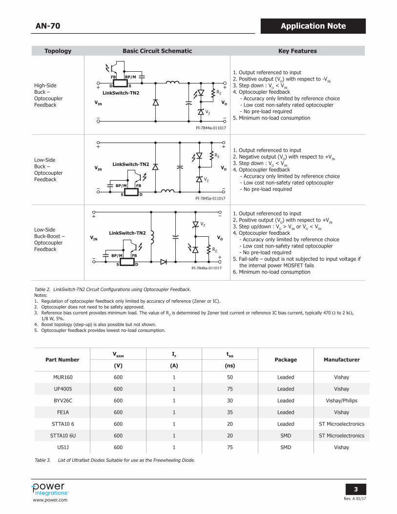
Topology Basic Circuit Schematic Key Features
High-Side Buck – Optocoupler Feedback
1. Output referenced to input 2. Positive output (VO) with respect to -VIN 3. Step down : VO < VIN 4. Optocoupler feedback - Accuracy only limited by reference choice - Low cost non-safety rated optocoupler - No pre-load required 5. Minimum no-load consumption
Low-Side Buck – Optocoupler Feedback
1. Output referenced to input 2. Negative output (VO) with respect to +VIN 3. Step down : VO < VIN 4. Optocoupler feedback - Accuracy only limited by reference choice - Low cost non-safety rated optocoupler - No pre-load required
Low-Side Buck-Boost – Optocoupler Feedback
1. Output referenced to input 2. Positive output (VO) with respect to +VIN 3. Step up/down : VO > VIN or VO < VIN 4. Optocoupler feedback - Accuracy only limited by reference choice - Low cost non-safety rated optocoupler - No pre-load required 5. Fail-safe – output is not subjected to input voltage if the internal power MOSFET fails 6. Minimum no-load consumption
Table 2. LinkSwitch-TN2 Circuit Configurations using Optocoupler Feedback.Notes:1. Regulation of optocoupler feedback only limited by accuracy of reference (Zener or IC).2. Optocoupler does not need to be safety approved.3. Reference bias current provides minimum load. The value of RZ is determined by Zener test current or reference IC bias current, typically 470 Ω to 2 kΩ,
1/8 W, 5%.4. Boost topology (step-up) is also possible but not shown.5. Optocoupler feedback provides lowest no-load consumption.
LinkSwitch-TN2
PI-7844a-011017
+ +
BP/MFB
D S
VOVIN
RZ
VZ
LinkSwitch-TN2
PI-7845a-011017
+ +
BP/M FB
DS
VOVIN
RZ
VZ
LinkSwitch-TN2
PI-7848a-011017
+
BP/M FB
DS
VOVIN
+RZ
VZ
Part NumberVRRM IF tRR
Package Manufacturer(V) (A) (ns)
MUR160 600 1 50 Leaded Vishay
UF4005 600 1 75 Leaded Vishay
BYV26C 600 1 30 Leaded Vishay/Philips
FE1A 600 1 35 Leaded Vishay
STTA10 6 600 1 20 Leaded ST Microelectronics
STTA10 6U 600 1 20 SMD ST Microelectronics
US1J 600 1 75 SMD Vishay
Table 3. List of Ultrafast Diodes Suitable for use as the Freewheeling Diode.
Rev. A 01/17
4
Application Note AN-70
www.power.com
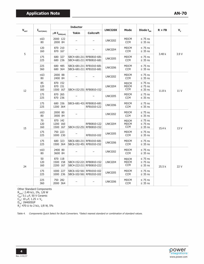
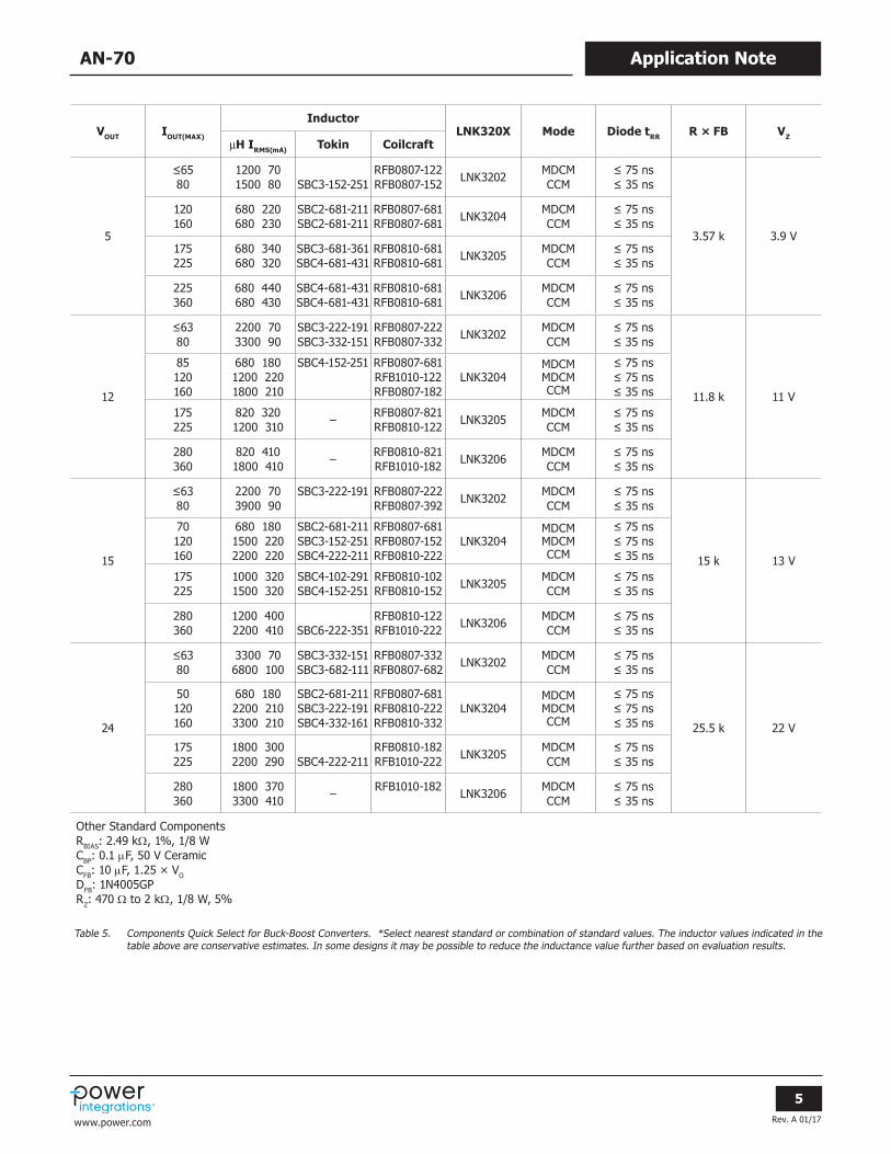
Table 4. Components Quick Select for Buck Converters. *Select nearest standard or combination of standard values.
VOUT IOUT(MAX)
InductorLNK320X Mode Diode tRR R × FB VZ
mH IRMS(mA) Tokin Coilcraft
5
≤63 80
2000 1222000 84 ‒ ‒ LNK3202 MDCM
CCM≤ 75 ns≤ 35 ns
3.48 k 3.9 V
120160
870 210870 167 ‒ ‒ LNK3204 MDCM
CCM≤ 75 ns≤ 35 ns
175225
680 327680 236
SBC4-681-211 SBC4-681-211
RFB0810-681 RFB0810-681 LNK3205 MDCM
CCM≤ 75 ns≤ 35 ns
225360
680 485680 364
SBC6-681-211 SBC6-681-211
RFB1010-681 RFB1010-681 LNK3206 MDCM
CCM≤ 75 ns≤ 35 ns
12
≤63 80
2000 882400 84 ‒ ‒ LNK3202 MDCM
CCM≤ 75 ns≤ 35 ns
11.8 k 11 V
85120160
870 152870 1511500 167 SBC4-152-251 RFB0810-152
LNK3204MDCM MDCM CCM
≤ 75 ns≤ 75 ns≤ 35 ns
175225
870 265870 236 ‒ ‒ LNK3205 MDCM
CCM≤ 75 ns≤ 35 ns
175225
680 3361200 364
SBC6-681-431 RFB0810-681 RFB1010-122 LNK3206 MDCM
CCM≤ 75 ns≤ 35 ns
15
≤63 80
2000 803000 84 ‒ LNK3202 MDCM
CCM≤ 75 ns≤ 35 ns
15.4 k 13 V
70120160
870 1421200 1601500 167 SBC4-152-251
RFB0810-122 RFB0810-152
LNK3204MDCM MDCM CCM
≤ 75 ns≤ 75 ns≤ 35 ns
175225
750 2231000 230 ‒ RFB1010-102 LNK3205 MDCM
CCM≤ 75 ns≤ 35 ns
175225
680 3231500 364
SBC6-681-211SBC6-152-451
RFB1010-681 RFB1010-152 LNK3206 MDCM
CCM≤ 75 ns≤ 35 ns
24
≤63 80
2400 803600 84 ‒ ‒ LNK3202 MDCM
CCM≤ 75 ns≤ 35 ns
25.5 k 22 V
50120160
870 1181500 1582200 167
SBC4-152-221 SBC4-222-211
RFB0810-152 RFB0810-222
LNK3204MDCM MDCM CCM
≤ 75 ns≤ 75 ns≤ 35 ns
175225
1000 2271000 236
SBC6-102-561SBC6-102-561
RFB1010-102 RFB1010-102 LNK3205 MDCM
CCM≤ 75 ns≤ 35 ns
225360
750 2822000 364 ‒ ‒ LNK3206 MDCM
CCM≤ 75 ns≤ 35 ns
Other Standard Components RBIAS: 2.49 kΩ, 1%, 1/8 W CBP: 0.1 mF, 50 V Ceramic CFB: 10 mF, 1.25 × VO DFB: 1N4005GP RZ: 470 Ω to 2 kΩ, 1/8 W, 5%
Rev. A 01/17
5
Application NoteAN-70
www.power.com
Table 5. Components Quick Select for Buck-Boost Converters. *Select nearest standard or combination of standard values. The inductor values indicated in the table above are conservative estimates. In some designs it may be possible to reduce the inductance value further based on evaluation results.
VOUT IOUT(MAX)
InductorLNK320X Mode Diode tRR R × FB VZ
mH IRMS(mA) Tokin Coilcraft
5
≤65 80
1200 701500 80 SBC3-152-251
RFB0807-122 RFB0807-152 LNK3202 MDCM
CCM≤ 75 ns≤ 35 ns
3.57 k 3.9 V
120160
680 220680 230
SBC2-681-211 SBC2-681-211
RFB0807-681 RFB0807-681 LNK3204 MDCM
CCM≤ 75 ns≤ 35 ns
175225
680 340680 320
SBC3-681-361 SBC4-681-431
RFB0810-681 RFB0810-681 LNK3205 MDCM
CCM≤ 75 ns≤ 35 ns
225360
680 440680 430
SBC4-681-431 SBC4-681-431
RFB0810-681 RFB0810-681 LNK3206 MDCM
CCM≤ 75 ns≤ 35 ns
12
≤63 80
2200 703300 90
SBC3-222-191 SBC3-332-151
RFB0807-222 RFB0807-332 LNK3202 MDCM
CCM≤ 75 ns≤ 35 ns
11.8 k 11 V
85120160
680 1801200 2201800 210
SBC4-152-251 RFB0807-681 RFB1010-122 RFB0807-182
LNK3204MDCM MDCM CCM
≤ 75 ns≤ 75 ns≤ 35 ns
175225
820 3201200 310 ‒ RFB0807-821
RFB0810-122 LNK3205 MDCM CCM
≤ 75 ns≤ 35 ns
280360
820 4101800 410 ‒ RFB0810-821
RFB1010-182 LNK3206 MDCM CCM
≤ 75 ns≤ 35 ns
15
≤63 80
2200 703900 90
SBC3-222-191 RFB0807-222 RFB0807-392 LNK3202 MDCM
CCM≤ 75 ns≤ 35 ns
15 k 13 V
70120160
680 1801500 2202200 220
SBC2-681-211 SBC3-152-251 SBC4-222-211
RFB0807-681 RFB0807-152 RFB0810-222
LNK3204MDCM MDCM CCM
≤ 75 ns≤ 75 ns≤ 35 ns
175225
1000 3201500 320
SBC4-102-291 SBC4-152-251
RFB0810-102 RFB0810-152 LNK3205 MDCM
CCM≤ 75 ns≤ 35 ns
280360
1200 4002200 410 SBC6-222-351
RFB0810-122 RFB1010-222 LNK3206 MDCM
CCM≤ 75 ns≤ 35 ns
24
≤63 80
3300 706800 100
SBC3-332-151 SBC3-682-111
RFB0807-332 RFB0807-682 LNK3202 MDCM
CCM≤ 75 ns≤ 35 ns
25.5 k 22 V
50120160
680 1802200 2103300 210
SBC2-681-211 SBC3-222-191 SBC4-332-161
RFB0807-681 RFB0810-222 RFB0810-332
LNK3204MDCM MDCM CCM
≤ 75 ns≤ 75 ns≤ 35 ns
175225
1800 3002200 290 SBC4-222-211
RFB0810-182 RFB1010-222 LNK3205 MDCM
CCM≤ 75 ns≤ 35 ns
280360
1800 3703300 410 ‒ RFB1010-182 LNK3206 MDCM
CCM≤ 75 ns≤ 35 ns
Other Standard Components RBIAS: 2.49 kΩ, 1%, 1/8 W CBP: 0.1 mF, 50 V Ceramic CFB: 10 mF, 1.25 × VO DFB: 1N4005GP RZ: 470 Ω to 2 kΩ, 1/8 W, 5%
Rev. A 01/17
6
Application Note AN-70
www.power.com
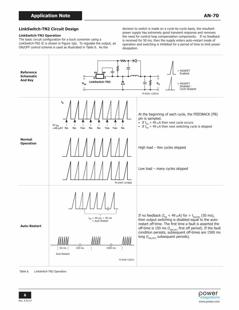
LinkSwitch-TN2 Circuit DesignLinkSwitch-TN2 OperationThe basic circuit configuration for a buck converter using a LinkSwitch-TN2 IC is shown in Figure 1(a). To regulate the output, an ON/OFF control scheme is used as illustrated in Table 6. As the
decision to switch is made on a cycle-by-cycle basis, the resultant power supply has extremely good transient response and removes the need for control loop compensation components. If no feedback is received for 50 ms, then the supply enters auto-restart mode of operation and switching is inhibited for a period of time to limit power dissipation.
ReferenceSchematicAnd Key
NormalOperation
At the beginning of each cycle, the FEEDBACK (FB) pin is sampled.• If IFB < 49 mA then next cycle occurs• If IFB > 49 mA then next switching cycle is skipped
High load – few cycles skipped
Low load – many cycles skipped
Auto-Restart
If no feedback (IFB < 49 mA) for > tAR(ON) (50 ms), then output switching is disabled equal to the auto-restart off-time. The first time a fault is asserted the off-time is 150 ms (tAR(OFF) first off period). If the fault condition persists, subsequent off-times are 1500 ms long (tAR(OFF) subsequent periods).
VOVIN
PI-8201-120516
+ +
FB BP
SD
LinkSwitch-TN2
= MOSFET Enabled
= MOSFET Disabled - Cycle Skipped
ID
No No Yes NoIs IFB >49 µA? No Yes Yes No
PI-3767-121903
IFB < 49 µA, > 50 ms= Auto-Restart
Auto-Restart
50 ms 150 ms 1500 ms
PI-8208-120616
Table 6. LinkSwitch-TN2 Operation.
Rev. A 01/17
7
Application NoteAN-70
www.power.com
To allow direct sensing of the output voltage without the need for a reference (Zener diode or reference IC), the FEEDBACK pin voltage is tightly toleranced over the entire operating temperature range. For example, this allows a 12 V design with an overall output tolerance of ±5%. For higher performance, an optocoupler can be used with a reference as shown in Table 2. Since the optocoupler just provides level shifting, it does not need to be safety rated or approved. The use of an optocoupler also allows flexibility in the location of the device, for example it allows a buck converter configuration with the LinkSwitch-TN2 IC in the low-side return rail, reducing EMI as the SOURCE pins and connected components are no longer part of the switching node.
Selecting the TopologyIf possible, use the buck topology. The buck topology maximizes the available output power from a given LinkSwitch-TN2 IC and inductor value. Also, the voltage stress on the power switch and freewheeling diode and the average current through the output inductor are slightly lower in the buck topology as compared to the buck-boost topology.
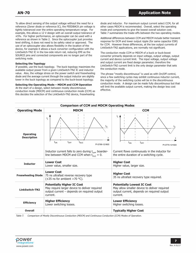
Selecting the Operating Mode – MDCM and CCM OperationAt the start of a design, select between mostly discontinuous conduction mode (MDCM) and continuous conduction mode (CCM) as this decides the selection of the LinkSwitch-TN2 device, freewheeling
diode and inductor. For maximum output current select CCM, for all other cases MDCM is recommended. Overall, select the operating mode and components to give the lowest overall solution cost. Table 7 summarizes the trade-offs between the two operating modes.
Additional differences between CCM and MDCM include better transient response for DCM and lower output ripple (for same capacitor ESR) for CCM. However these differences, at the low output currents of LinkSwitch-TN2 applications, are normally not significant.
The conduction mode CCM or MDCM of a buck or buck-boost converter primarily depends on input voltage, output voltage, output current and device current limit. The input voltage, output voltage and output current are fixed design parameter; therefore the LinkSwitch-TN2 current limit is the only design parameter that sets the conduction mode.
The phrase “mostly discontinuous” is used as with On/Off control, since a few switching cycles may exhibit continuous inductor current, the majority of the switching cycles will be in the discontinuous conduction mode. A design can be made fully discontinuous but that will limit the available output current, making the design less cost effective.
Comparison of CCM and MDCM Operating Modes
Operating Mode MDCM CCM
OperatingDescription
Inductor current falls to zero during tOFF, boarder-line between MDCM and CCM when tIDLE = 0.
Current flows continuously in the inductor for the entire duration of a switching cycle.
Inductor Lower Cost Lower value, smaller size.
Higher CostHigher value, larger size.
Freewheeling DiodeLower Cost 75 ns ultrafast reverse recovery type (≤35 ns for ambient >70 °C).
Higher Cost35 ns ultrafast recovery type required.
LinkSwitch-TN2
Potentially Higher IC Cost May require larger device to deliver required output current – depends on required output current.
Potentially Lowest IC Cost May allow smaller device to deliver required output current, depends on required output current.
Efficiency Higher Efficiency Lower switching losses.
Lower Efficiency Higher switching losses.
Overall Typically Higher Cost
PI-3769-121803
IL
tON tOFF tIDLE
t
IO
PI-3770-121503
IL
tON tOFF
t
IO
Table 7. Comparison of Mostly Discontinuous Conduction (MDCM) and Continuous Conduction (CCM) Modes of Operation.

Rev. A 01/17
8
Application Note AN-70
www.power.com
Step-by-Step Design ProcedureStep 1 ‒ Enter Application Variables VACMIN, VACMAX, fL,
VO, IO, η, CIN
Input VoltageDetermine the input voltage range from Table 8.
Line Frequency, fL50 Hz for universal or single 100 VAC, 60 Hz for single 115 VAC input. 50 Hz for single 230 VAC input. These values represent typical line frequencies rather than minimum. For most applications this gives adequate overall design margin. For absolute worst case or based on the product specification reduce these numbers by 6% (47 Hz or 56 Hz). For half-wave rectification use fL/2.
Nominal Output Voltage, VOUT (V)Enter the nominal output voltage of the main output during the continuous load condition. Generally the main output is the output from which feedback is derived.
Output Power, IOUT (A)Enter the output current of the power supply. If the power supply is a multiple output power supply, enter the sum total equivalent current of all the outputs, sum total power divide the main output voltage.
In multiple output designs the output power of the main output (typically the output from which feedback is taken) should be increased such that the maximum continuous output power as
applicable matches the sum of the output power from all the outputs in the design. The individual output voltages and currents should then be entered at the bottom of the spreadsheet
Power Supply Efficiency, ηEnter the estimated efficiency of the complete power supply measured at the output terminals under peak load conditions and worst-case line (generally lowest input voltage). Start with a value of 0.7 for a 12 V output, 0.55 for a 5 V output if no better reference data available, typical for a design where the majority of the output power is drawn from an output voltage of 12 V or greater. Once a prototype has been constructed then the measured efficiency should be entered.
Total Input Capacitance, CIN (mF)Enter total input capacitance using Table 9 for guidance.
The capacitance is used to calculate the minimum and maximum DC voltage across the bulk capacitor and should be selected to keep the minimum DC input voltage, VMIN > 70 V.
Figure 2. Application Variable Section of LinkSwitch-TN2 Design Spreadsheet.
Nominal Input Voltage (VAC) VACMIN VACMAX
100/115 85 132
230 195 265
Universal 85 265
Table 8. Standard Worldwide Input Line Voltage Ranges.
Total Input Capacitance per Watt Output Power mF/W
AC Input Voltage(VAC)
Full-Wave Rectification
Half-Wave Rectification
100/115 2 4-5
230 1 1-2
85-265 2 4-5
Table 9. Suggested Total Input Capacitance Values for Different Input Voltage Ranges.
ENTER APPLICATION VARIABLESLINE VOLTAGE RANGE Universal AC line voltage rangeVACMIN 85.00 85.00 volts AC Minimum AC line voltageVACTYP 115.00 volts AC Typical AC line voltageVACMAX 265.00 265.00 volts AC Maximum AC line voltagefL 50.00 Hz AC mains frequencyLINE RECTIFICATION TYPE H H Select 'F'ull wave rectification or 'H'alf wave rectificationt_CONDUCTION 2.72 ms Enter the bridge diode conduction timeVOUT 12.00 12.00 volts DC Output voltageIOUT 0.120 0.120 A Average output currentEFFICIENCY_ESTIMATED 0.75 Efficiency estimate at output terminalsEFFICIENCY_CALCULATED 0.82 Calculated efficiency based on real components and operating pointPOUT 1.44 W Continuous Output PowerCIN 9.40 9.40 uF Input capacitorVMIN 86.0 volts DC Valley of the rectified input voltageVMAX 374.8 volts DC Peak of the rectified maximum input AC voltageT_AMBIENT 50 degC Operating ambient temperature in degrees celciusINPUT STAGE RESISTANCE 10 mohms Input stage resistance in milliohms (includes fuse, thermistor, filtering components)PLOSS_INPUTSTAGE 0.000 W Input stage losses estimate

Rev. A 01/17
9
Application NoteAN-70
www.power.com
Step 2 – Determine AC Input Stage
The input stage comprises fusible resistor(s), input rectification diodes and line filter network. Flameproof fusible resistors are recommended to be chosen and depending on the differential line input surge requirements, a wire-wound type may be required. The fusible resistor(s) provides fuse safety, inrush current limiting and differential mode noise attenuation. The EMI performance of half-wave rectified designs is improved by adding a second diode in the lower return rail. This provides EMI gating (EMI currents only flow when the diode is conducting) and also doubles differential surge withstand as the surge voltage is shared across two diodes. Table 10 shows the recommended input stage based on output power for a universal input design while Table 9 shows how to adjust the input capacitance for other input voltage ranges.
Step 3 – Determine Minimum and Maximum DC Input Voltages VMIN and VMAX Based on AC Input Voltage
Calculate VMAX as:
#V V2MAX ACMAX= (1)
Assuming that the value of input fusible resistor is small, the voltage drop across it can be ignored.
Derive minimum input voltage VMIN.
Half bridge rectifier:
V V C
P f t2
2 1
MIN ACMININ TOTAL
OL
C2# #
#
h= --
^b^
hl
h (2)
Full bridge rectifier:
V V C
P tf2
2 12
MIN ACMININ TOTAL
O CL2# #
# #h= -
-^
b^
hl
h (3)
If VMIN is ≤ 70 V then increase value of CIN(TOTAL). tC is the bridge diode conduction time.
Step 4 – Select LinkSwitch-TN2 Device Based on Output Current and Current Limit
Decide on the operating mode ‒ refer to Table 7.
For MDCM operation, the output current (IO) should be less than or equal to half the value of the minimum current limit of the chosen device from the data sheet.
#I I2>_LIMIT MIN O (4)
For CCM operation, the device should be chosen such that the output current IO, is more than 50%, but less than 80% of the minimum current limit ILIMIT_MIN.
< <# #. .I I I0 5 0 8_ _LIMIT MIN O LIMIT MIN (5)
Please see the data sheet for LinkSwitch-TN2 current limit values.
A typical LinkSwitch-TN2 part can be programmed to operate in one of the two current limits. The “RED” or reduced current limit enables operation at a reduced current limit and is recommended when the part is to be used at a current level considerably lower than the rated output current. A “STD” or standard current limit will be selected in most applications to optimize on BP capacitor cost.
Use of a 0.1 mF capacitor results in the standard current limit value. Use of a 1 mF capacitor results in the current limit being reduced, allowing design with lowest cost surface mount buck chokes.
POUT ≤0.25 W 0.25 - 1 W >1 W
85 - 265 VACInput Stage
RF1, RF2: 100-470 Ω, 0.5 W, FusibleCIN: ≥2.2 mF, 400 VDIN1, DIN2: 1N4007, 1 A, 1000 V
RF1: 8.2 Ω, 1 W FusibleRF2: 100 Ω, 0.5 W, FlameproofCIN1, CIN2: ≥3.3 mF, 400 V eachDIN1, DIN2: 1N4007, 1 A, 1000 V
RF1: 8.2 Ω, 1 W FusibleLIN: 470 mH ‒ 2.2 mH, 0.05 A ‒ 0.3 ACIN1, CIN2: ≥4 mF/WOUT, 400 V
eachDIN1, DIN2: 1N4007, 1 A, 1000 V
RF1: 8.2 Ω, 1 W FusibleLIN: 470 mH ‒ 2.2 mH, 0.05 A ‒ 0.3 ACIN1, CIN2: ≥2 mF/WOUT, 400 V
eachDIN1, DIN2: 1N4007, 1 A, 1000 V
Comments *Optional for improved EMI and line surge performance. Remove for designs requiring no impedance in return rail.**Increase value to meet required differential line surge performance.
PI-3771-121603
+
ACIN
RF1
RF2
DIN1
DIN2
CIN**
* *
PI-3772-121603
+
ACIN
RF1 RF2DIN1
DIN2
**
*
CIN2CIN1
PI-3773-121603
+
ACIN
RF1LINDIN1
DIN2
**
*
CIN2CIN1
PI-3774-121603
+
AC IN
RF1LIN
DIN1-4
CIN2CIN1**
Table 10. Recommended AC Input Stages for Universal Input.
Rev. A 01/17
10
Application Note AN-70
www.power.com
Step 5 ‒ Select the Output Inductor
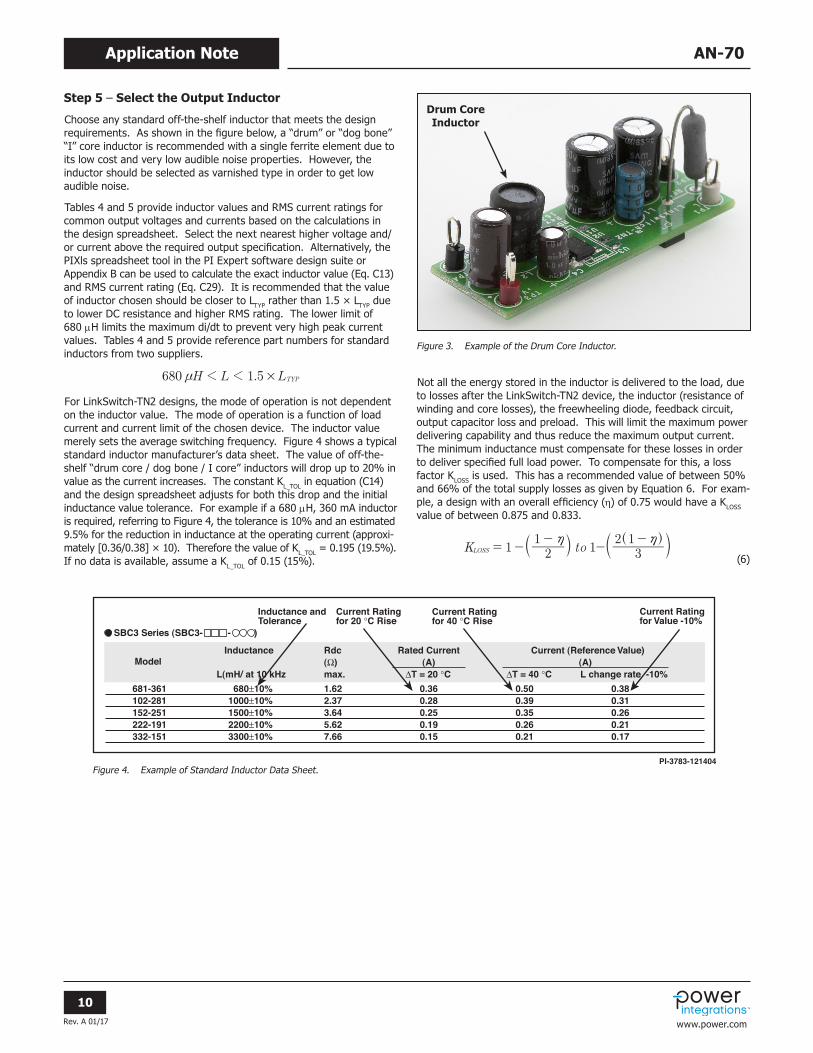
Choose any standard off-the-shelf inductor that meets the design requirements. As shown in the figure below, a “drum” or “dog bone” “I” core inductor is recommended with a single ferrite element due to its low cost and very low audible noise properties. However, the inductor should be selected as varnished type in order to get low audible noise.
Tables 4 and 5 provide inductor values and RMS current ratings for common output voltages and currents based on the calculations in the design spreadsheet. Select the next nearest higher voltage and/or current above the required output specification. Alternatively, the PIXls spreadsheet tool in the PI Expert software design suite or Appendix B can be used to calculate the exact inductor value (Eq. C13) and RMS current rating (Eq. C29). It is recommended that the value of inductor chosen should be closer to LTYP rather than 1.5 × LTYP due to lower DC resistance and higher RMS rating. The lower limit of 680 mH limits the maximum di/dt to prevent very high peak current values. Tables 4 and 5 provide reference part numbers for standard inductors from two suppliers.
.H L L680 1 5 TYP#1 1n
For LinkSwitch-TN2 designs, the mode of operation is not dependent on the inductor value. The mode of operation is a function of load current and current limit of the chosen device. The inductor value merely sets the average switching frequency. Figure 4 shows a typical standard inductor manufacturer’s data sheet. The value of off-the-shelf “drum core / dog bone / I core” inductors will drop up to 20% in value as the current increases. The constant KL_TOL in equation (C14) and the design spreadsheet adjusts for both this drop and the initial inductance value tolerance. For example if a 680 mH, 360 mA inductor is required, referring to Figure 4, the tolerance is 10% and an estimated 9.5% for the reduction in inductance at the operating current (approxi-mately [0.36/0.38] × 10). Therefore the value of KL_TOL = 0.195 (19.5%). If no data is available, assume a KL_TOL of 0.15 (15%).
Not all the energy stored in the inductor is delivered to the load, due to losses after the LinkSwitch-TN2 device, the inductor (resistance of winding and core losses), the freewheeling diode, feedback circuit, output capacitor loss and preload. This will limit the maximum power delivering capability and thus reduce the maximum output current. The minimum inductance must compensate for these losses in order to deliver specified full load power. To compensate for this, a loss factor KLOSS is used. This has a recommended value of between 50% and 66% of the total supply losses as given by Equation 6. For exam-ple, a design with an overall efficiency (η) of 0.75 would have a KLOSS value of between 0.875 and 0.833.
K to 1-1 2
1 -3
2 1 -LOSS
h h= - b c ^l h m
(6)
Figure 3. Example of the Drum Core Inductor.
Inductance and Tolerance
SBC3 Series (SBC3- - )
681-361 680±10% 1.62 0.36 0.50 0.38102-281 1000±10% 2.37 0.28 0.39 0.31152-251 1500±10% 3.64 0.25 0.35 0.26222-191 2200±10% 5.62 0.19 0.26 0.21332-151 3300±10% 7.66 0.15 0.21 0.17
Current Ratingfor 20 °C Rise
Current Ratingfor 40 °C Rise
Current Ratingfor Value -10%
Inductance Rdc Rated Current Current (Reference Value) (Ω) (A) (A) L(mH/ at 10 kHz max. ∆T = 20 °C ∆T = 40 °C L change rate -10% Model
PI-3783-121404Figure 4. Example of Standard Inductor Data Sheet.
Drum CoreInductor

Rev. A 01/17
11
Application NoteAN-70
www.power.com
Step 6 ‒ Select Freewheeling Diode
For MDCM operation at tAMB ≤ 70 °C, select an ultrafast diode with tRR ≤ 75 ns. At tAMB > 70 °C, tRR ≤ 35 ns. For CCM operation, select an ultrafast diode with tRR ≤ 35 ns. Allowing 25% design margin for the freewheeling diode,
.V V1 25PIV MAX#2 (7)
The diode must be able to conduct the full load current. Thus:
.I I1 25F O#2 (8)
Table 3 lists common freewheeling diode choices.
Step 7 ‒ Select Output Capacitor
The output capacitor should be chosen based on the output voltage ripple requirement. Typically the output voltage ripple is dominated by the capacitor ESR and can be estimated as:
ESR I
VMAX
RIPPLE
RIPPLE= (9)
where VRIPPLE is the maximum output ripple specification and IRipple is the LinkSwitch-TN2 output ripple current (Refer to C2 and C3).
The capacitor ESR value should be specified approximately at the switching frequency of 66 kHz. Capacitor values above 100 mF are not recommended as they can prevent the output voltage from reaching regulation during the 50 ms period prior to auto-restart. If more capacitance is required, then a soft-start capacitor should be added (see Tips for Designs section). Select a voltage rating such that VRATED ≥1.25 × VO.
Step 8 ‒ Select the Feedback Resistors
The values of RFB and RBIAS are selected such that, at the regulated output voltage, the voltage on the FEEDBACK pin (VFB) is 2 V. This voltage is specified for a FEEDBACK pin current (IFB) of 49 mA.
Let the value of RBIAS = 2.49 kΩ; this biases the feedback network at a current of ~0.8 mA. Hence the value of RFB is given by:
R
RV I
V V V VV I R
RFB
BIAS
FBFB
O FB O FB
FB FB BIAS
BIAS
##
=+
-=
-+
^^h
h (10)
Step 9 ‒ Select the Feedback Diode and Capacitor
For the feedback capacitor, use a 10 mF general purpose electrolytic capacitor with a voltage rating ≥1.25 × VO. For the feedback diode, use a glass passivated 1N4005GP or 1DFLR1600-7 device with a voltage rating of ≥1.25 × VMAX.
Step 10 ‒ Select the External Biased Resistor for BYPASS Pin
To reduce the no-load input power of the power supply, resistor R5 in Figure 9 of the application example, connected from the feedback capacitor C3 to the BYPASS pin, is recommended. This is applicable to the power supply whose output voltage is higher than VBP(SHUNT).
To achieve lowest no load power consumption, the current fed into the BYPASS pin should be slightly higher than 120 mA. For the best full load efficiency and thermal performance, the current fed into the BYPASS pin should be slightly higher than the current value stated below:
The BYPASS pin current should not exceed 16 mA (IBP(MAX)) at the maximum output voltage (normally when the output voltage is at no-load condition).
Step 11 ‒ Select Pre-Load ResistorIn high-side, direct feedback designs where the minimum load is <3 mA, a pre-load resistor is required to maintain output regulation. This ensures sufficient inductor energy to pull the inductor side of the feedback capacitor CFB to input return via DFB. The value of RPL should be selected to give a minimum output load of 3 mA.
In designs with an optocoupler a Zener diode or reference bias current provides a 1 mA to 2 mA minimum load, preventing “pulse bunching” and increased output ripple at zero load.
Part Number Bypass Current
LNK3202 195 mA
LNK3204 222 mA
LNK3205 269 mA
LNK3206 290 mA
Table 11. Bypass Pin Injection Current when MOSFET is Switching.
Rev. A 01/17
12
Application Note AN-70
www.power.com
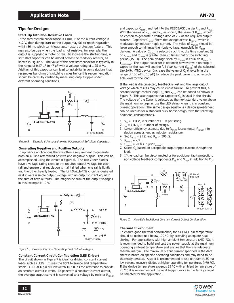
Tips for DesignsStart-Up Into Non-Resistive Loads If the total system capacitance is >100 mF or the output voltage is >12 V, then during start-up the output may fail to reach regulation within 50 ms which can trigger auto-restart protection feature. This may also be true when the load is not resistive, for example, the output is supplying a motor or fan. To increase the start-up time, a soft-start capacitor can be added across the feedback resistor, as shown in Figure 5. The value of this soft-start capacitor is typically in the range of 0.47 mF to 47 mF with a voltage rating of 1.25 × VO. Addition of this capacitor can lead to instability in some designs that resembles bunching of switching cycles hence this recommendation should be carefully verified by measuring output ripple under different operating conditions.
Generating Negative and Positive Outputs In appliance applications there is often a requirement to generate both an AC line referenced positive and negative output. This can be accomplished using the circuit in Figure 6. The two Zener diodes have a voltage rating close to the required output voltage for each rail and ensure that regulation is maintained when one rail is lightly and the other heavily loaded. The LinkSwitch-TN2 circuit is designed as if it were a single output voltage with an output current equal to the sum of both outputs. The magnitude sum of the output voltages in this example is 12 V.
Constant Current Circuit Configuration (LED Driver) The circuit shown in Figure 7 is ideal for driving constant current loads such as LEDs. It uses the tight tolerance and temperature stable FEEDBACK pin of LinkSwitch-TN2 IC as the reference to provide an accurate output current. To generate a constant current output, the average output current is converted to a voltage by resistor RSENSE
and capacitor CSENSE and fed into the FEEDBACK pin via RFB and RBIAS. With the values of RBIAS and RFB as shown, the value of RSENSE should be chosen to generate a voltage drop of 2 V at the required output current. Capacitor CSENSE filters the voltage across RSENSE, which is modulated by inductor ripple current. The value of CSENSE should be large enough to minimize the ripple voltage, especially in MDCM designs. A value of CSENSE is selected such that the time constant (t) of RSENSE and CSENSE is greater than 20 times that of the switching period (15 ms). The peak voltage seen by CSENSE is equal to RSENSE × ILIMIT(MAX). The output capacitor is optional; however with no output capacitor the load will see the full peak current (ILIMIT) of the selected LinkSwitch-TN2 device. Increase the value of CO (typically in the range of 100 nF to 10 mF) to reduce the peak current to an accept-able level for the load.
If the load is disconnected, feedback is lost and the large output voltage which results may cause circuit failure. To prevent this, a second voltage control loop, DFB and VRFB, can be added as shown in Figure 7. This also requires that capacitor CO is used in the circuit. The voltage of the Zener is selected as the next standard value above the maximum voltage across the LED string when it is in constant current operation. The same design equations / design spreadsheet can be used as for a standard buck-boost design, with the following additional considerations.
1. VO = LED VF × Number of LEDs per string.2. IO = LED IF × Number of strings.3. Lower efficiency estimate due to RSENSE losses (enter RSENSE into
design spreadsheet as inductor resistance).4. Set RBIAS = 2 kΩ and RFB = 300 Ω.5. RSENSE = 2/IO.6. CSENSE = 20 × (15 ms/RSENSE).7. Select CO based on acceptable output ripple current through the
load.8. If the load can be disconnected or for additional fault protection,
add voltage feedback components DFB and VRFB, in addition to CO.
Thermal Environment To ensure good thermal performance, the SOURCE pin temperature should be maintained below 100 °C, by providing adequate heat sinking. For applications with high ambient temperature (>50 °C), it is recommended to build and test the power supply at the maximum operating ambient temperature and ensure that there is adequate thermal margin. The maximum output current specified in the data sheet is based on specific operating conditions and may need to be thermally derated. Also, it is recommended to use ultrafast (≤35 ns) low reverse recovery diodes at higher operating temperatures (>70 °C). If the device temperature exceeds 85 °C with ambient temperature of 25 °C, it is recommended the next bigger device in the family should be selected for the application.
Figure 5. Example Schematic Showing Placement of Soft-Start Capacitor.
+7 V
RTN
-5 V
VIN
5.1 V
6.8 V
PI-8203-120516
+
FB BP
SD
LinkSwitch-TN2
OptionalSee Text
RSENSE
RFB300 Ω
RBIAS2 kΩ
IO
CO L
CSENSE
DFW
VRFB DFB
VIN
PI-8204-120516
+
FB BP
SDLinkSwitch-TN2
Figure 7. High-Side Buck-Boost Constant Current Output Configuration.
Figure 6. Example Circuit – Generating Dual Output Voltages.
VOVIN
CSS
RFB
PI-8202-120516
+ +
FB BP
SD
LinkSwitch-TN2

Rev. A 01/17
13
Application NoteAN-70
www.power.com
A battery powered thermocouple meter is recommended to make measurements when the SOURCE pins are a switching node. Alternatively, the ambient temperature may be raised to indicate margin to thermal shutdown.
Recommended Layout ConsiderationsIn the buck or buck-boost converter configuration, since the SOURCE pins in LinkSwitch-TN2 devices are switching nodes, the copper area connected to SOURCE should be minimized to minimize EMI within the thermal constraints of the design.
In the boost configuration, since the SOURCE pins are tied to DC return, the copper area connected to SOURCE can be maximized to improve heat sinking.
Figure 8 are printed circuit board layout design examples for the circuit schematic shown in Figure 9. The loop formed between the LinkSwitch-TN2, inductor (L1), freewheeling diode (D1), and output capacitor (C2) should be kept as small as possible. The loop between the input capacitor C5, IC DRAIN pin, SOURCE pin, freewheeling diode cathode and anode should be as small as possible. The BYPASS pin capacitor C1 (Figure 9) should be located physically close to the SOURCE and BYPASS pins.
Most off-the-shelf inductors are drum core inductors or dogbone inductors. These inductors do not have a good closed magnetic path, and are a source of significant magnetic coupling. They are a source of differential mode noise. To minimize direct coupling from switching nodes, the LinkSwitch-TN2 IC should be placed away from AC input lines. It may be advantageous to place capacitors C4 and C5 in-between LinkSwitch-TN2 device and the AC input. In a drum core inductor, the winding is typically wound in multiple layers. In a given design, result of EMI performance and regulation can change depend-
ing on which end of the inductor is connected to the output capacitor and which end is connected to the SOURCE pin of the IC. It is therefore recommended that effect of change of orientation of the inductor be verified and the favorable inductor orientation be used. Once the favorable orientation is determined, the same should be consistently followed on all boards manufactured so as to ensure repeatable performance. Typically inductors are marked to indicate the start and end of the windings. These markings can be used to correctly orient the inductors during assembly.
The second rectifier diode D4 is optional, but may be included for better EMI performance and higher line surge withstand capability.
Traces carrying high currents should be as short in length and thick in width as possible. These are the traces which connect the input capacitor, LinkSwitch-TN2 IC, inductor, freewheeling diode, and the output capacitor.
Design for Safety Compliance Power supplies are required to have capability of withstanding surge voltages which typically are a result of events such as lightning strikes. It is expected that such events do not lead to failure of any components or loss of functionality. Standards such as IEC61000-4-5 defines surge voltage and current waveforms as well as source impedance, which emulate typical worst case transients for testing of protection mechanisms for line connected power circuits and data line connected equipment.
Components of the fusible resistor, EMI filter and the capacitors used in the power supply input stage, help in limiting the voltage and current stress that the components of the power supply are subjected to during these events.
Figure 8. Recommended Printed Circuit Layout for LinkSwitch-TN2 using D Package. PI-8209-120616
Inductor away from the AC input lines
C4 and C5 in-betweenLinkSwitch-TN2 and AC input
Copper area should beminimized to minimize EMIwithin the thermalconstraints of the design
Traces carrying high switching current should be short
Rev. A 01/17
14
Application Note AN-70
www.power.com
MOVs will often be required to be added at the input of the power supply if the surge level is high (DM surge > 1 kV). These MOVs are placed after the input fuse and help in clamping the voltage at the input of the power supply when a surge event occurs.
The following checklist can be used to ensure that the design is compliant to the applicable requirements:
• Define the target market for LinkSwitch-TN2 converter.• Determine the equipment class to determine common-mode (CM)
and differential-mode (DM) surge levels.• If DM surge >1000 V, then you will likely need to include an MOV
across the AC line at the front-end of the EMI filter • Select a MOV for North America 115 VAC or universal input with
adequate stand-off voltage during normal operation as well as adequate rated surge current and energy capacity.
• An example of selecting an MOV: Assume that you have a North America application within a Class 3 equipment installation for which you need to select a MOV for differential mode protection, connected across the AC line. The DM Spike Energy will be less than 6.9 J. A device rated for 150 VAC continuous operation would provide adequate stand-off voltage for 115 VAC nominal applica-tions. Littlefuse part number V150LA5 provides 25 J and 2500 A surge capability with adequate margin to minimize degraded performance due to accumulated strikes over the life of the MOV. For a universal input design, the V320LA10 provides 48 J and 2500 A surge capability.
• Conduct both common-mode and differential-mode surge tests on the converter and observe voltages across key components and currents where necessary to validate SOA operation of components.
Verify all voltage and current extremes are within the rated specification of each X and Y capacitor. If not, specify a compo-nent with a higher rating.
• Verify surge transient current rating of the diode bridge used.• Verify MOSFET switch BV rating is greater than surge voltage on
switching node. If not, you may need to increase bulk capacitor size to prevent the surge energy from increasing the capacitor voltage to objectionable levels.
• Ensure that bulk capacitor surge voltage rating is not exceeded during testing. If surge voltage rating is exceeded, you may need to increase capacitance. Some capacitors may tolerate higher than the rated surge voltage for short durations however capacitor manufacturers should be consulted for guidance.
• Select an AC line fusible resistor which has an I2t rating that will accommodate power-on inrush current at maximum line voltage and which is rated for continuous AC line current and will not interrupt due to surge I2t. Do not oversize the fuse more than necessary to withstand transient currents so as to ensure that the fuse will interrupt line current in the event of a line-to-line MOV failure.
When making measurements on a power supply during a line surge or safety test, care should be taken to ensure that the test equipment is galvanically isolated. If alternate paths for the surge energy are created as a result of connection of test probes, the test result will be incorrect. Care must be taken to use voltage probes that are rated for measurement of high-voltages in excess of the voltages likely to be encountered during the test.
Rev. A 01/17
15
Application NoteAN-70
www.power.com
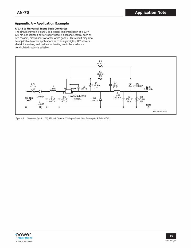
Appendix A – Application ExampleA 1.44 W Universal Input Buck ConverterThe circuit shown in Figure 9 is a typical implementation of a 12 V, 120 mA non-isolated power supply used in appliance control such as rice cookers, dishwashers or other white goods. This circuit may also be applicable to other applications such as night-lights, LED drivers, electricity meters, and residential heating controllers, where a non-isolated supply is suitable.
Figure 9. Universal Input, 12 V, 120 mA Constant Voltage Power Supply using LinkSwitch-TN2.
RTN
12 V,120 mA
85-265VAC
PI-7857-092616
FB BP/M
SD
LinkSwitch-TN2C44.7 µF400 V
C1100 nF
D41N4007
D31N4007
D1UF4005LNK3204
D21N4005GP
C2100 µF16 V
RF18.2 Ω2 W
R111.8 kΩ
1%
R526.7 kΩ
R32.49 kΩ
1%L21 mH
L11 mH
280 mAC54.7 µF400 V
C310 µF25 V
R43.3 kΩ
1%

Rev. A 01/17
16
Application Note AN-70
www.power.com
Figure 10. Inductor Voltage and Inductor Current of a Buck Converter in DCM.
Appendix BCalculations for Inductor Value for Buck and Buck-Boost TopologiesThere is a minimum value of inductance that is required to deliver the specified output power, regardless of line voltage and operating mode.
As a general case, Figure 10 shows the inductor current in discontinu-ous conduction mode (DCM). The following expressions are valid for both CCM as well as DCM operation. There are three unique intervals in DCM as can be seen from Figure 10. Interval tON is when the LinkSwitch-TN2 IC is ON and the freewheeling diode is OFF. Current ramps up in the inductor from an initial value of zero. The peak current is the current limit ILIMIT of the device. Interval tOFF is when the LinkSwitch-TN2 IC is OFF and the freewheeling diode is ON. Current ramps down to zero during this interval. Interval tIDLE is when both the LinkSwitch-TN2 IC and freewheeling diode are OFF, and the inductor current is zero.
In CCM, this idle state does not exist and thus tIDLE = 0.
We can express the current swing at the end of interval tON in a buck converter as:
(C1)
(C2)
(C3)
where IRIPPLE = Inductor ripple current ILIMIT_MIN = Minimum current limit VMIN = Minimum DC bus voltage VDS = On-state Drain to Source voltage drop VO = Output voltage LMIN = Minimum inductance
Similarly, we can express the current swing at the end of interval tOFF as:
I t I LV V
tOFF RIPPLEMIN
O FDOFF#D = =
+^ h (C4)
PI-3778-121803
ILimit
VIN-VO
VO
VL
IL
tON tOFF tIDLE
IO
t
t
The initial current through the inductor at the beginning of each switching cycle can be expressed as:
I I IINITIAL LIMIT MIN RIPPLE_= - (C5)
The average current through the inductor over one switching cycle is equal to the output current IO. This current can be expressed as: I T
I I t
I I t t
1 21
21
0_
_
_
OSW MAX
LIMIT MIN INITIAL ON
LIMIT MIN INITIAL OFF IDLE
# # #
# #=
+ +
+ +f^
^
h
hp
(C6)
WhereIO = Output current. TSW_MAX = The switching interval corresponding to minimum switching frequency FSMIN.
Substituting for tON and tOFF from equations (C1) and (C4) we have:
)I T
I I V V VI L
I I V VI L
t
1 21
21_
_
_
OSW MAX
LIMIT MIN INITIALMIN DS O
RIPPLE MIN
LIMIT MIN INITIALO FD
RIPPLE MINIDLE
# ##
# ##=
+ - - +
+ + +
J
L
KKKK
^
^
N
P
OOOO
h
h
(C7)
LI I FS V V V
V V I V V V2MI
LIM MIN INITIAL MIN MIN DS FD
O FD O MIN DS ON 2 2 # #
# # #=
- - ++ - -
-^
] ]
]h
g g
g (C8)
For MDCM design, IINITIAL = 0, IRIPPLE = ILIMIT_MIN.
LI FS V V VV V I V V V2
MILIM MIN MIN MIN DS FD
O FD O MIN DS ON 2
_ # ## # #
=- +
+ - -]]]g
gg
(C9)
For CCM design, tIDLE = 0.
I I I2
1O LIMIT MIN INITIAL#= +-
^ h (C10)
I IINITIAL LIM MIN= - (C11)
LI FS V V VV V V V V
I2MIM
LIM MIN MIN MIN DS FD
O FD MIN DS O
O # ##
#=
- ++ - --
-^
] ]
]h
g g
g (C12)
For output voltages greater than 20 V, use VMAX for calculation of LMIN (Equation C8). For output voltages less than 20 V, use VMIN for calculation of LMIN to compensate for current limit delay time over- shoot.
This however does not account for the losses within the inductor (resistance of winding and core losses) and the freewheeling diode, which will limit the maximum power delivering capability and thus reduce the maximum output current. The minimum inductance must compensate for these losses in order to deliver specified full load power. An estimate of these losses can be made by estimating the total losses in the power supply, and then allocating part of these losses to the inductor and diode. This is done by the loss factor KLOSS which increases the size of the inductor accordingly. Furthermore, typical inductors for this type of application are bobbin core or dog bone chokes. The specified current rating refer to a temperature rise of 20 °C or 40 °C and to an inductance drop of 10%. We must
I t I LV V V
t
I I I t for CCM
I I t for CMMD
2 0
2 0>
_
_ ,
ON RIPPLEMIN
MIN DS OON
RIPPLE LIMIT MIN O IDLE
RIPPLE LIMIT MIN IDLE
#
#
#
D = =- -
= - =
=
]
^
^ ^
^
g
h
h
h
h

Rev. A 01/17
17
Application NoteAN-70
www.power.com
incorporate an inductance tolerance factor KL_TOL within the expression for minimum inductance, to account for this manufacturing tolerance. The typical inductance value thus can be expressed as:
L
KK
L1TYP
L TOL
LOSS
MIN#=
+ -^ h
(C13)
where KLOSS is a loss factor, which accounts for the off-state total losses of the inductor.
KL_TOL is the inductor tolerance factor and can be between 10% and 20%. A typical value is 0.15. With this typical inductance we can express maximum output power as:
V V V V V
P L FS I I
V V V V
KK
2 1
_ _
MIN DS O O FD
O MAX TYP MIN LIMIT MIN INITIAL
O MIN DS FD
L
LOSS
2 2
TOL# #
# # #
##
- - +
= -
- +
+-
^
^
^
^ ^h
h
h
h
h
(C14)
Similarly for buck-boost topology the expressions for LTYP and PO_MAX are:
K I I FS
V V V V
L K V V
I V V
2 1
_
_
LOSS LIMIT MIN INITIAL MIN
MIN DS FD O
TYP L TOL O FD
O MIN DS
2 2# # #
# #
#-
- + +
= + +
-
]
^
^
]
^h
h
g
g
h
(C15)
V V V V
P L FS I I
V V V V VK
K2 1MIN DS O FD
O MAX TYP MIN LIMIT MIN INITIAL
O MIN DS FD O
L
LOSS
2 2
TOL# #
# # #
##
- +
= -
- + ++
- -
-^^
^
^ ^hhh
h
h (C16)
Average Switching Frequency Since LinkSwitch-TN2 uses an on-off type of control, the frequency of switching is non-uniform due to cycle skipping. We can average this switching frequency by substituting the maximum power as the output power in Equation C14. Simplifying, we have:
K I I
L V V V
FS K V V
I V V V
2 1
_
_
LOSS LIMIT MIN INITIAL
TYP MIN DS FD
AVG L TOL O FD
O MIN DS O
2 2# #
#
# # #
#-
- +
= + +
- -
^
]
^
]
^h
g
h
g
h
(C17)
Similarly for buck-boost converter, simplifying Equation C16 we have:
K I I
L V V V V
FS K V V
I V V
2 1
_
_
LOSS LIMIT MIN INITIAL
TYP MIN DS FD O
AVG L TOL O FD
O MIN DS
2 2# #
#
# #
#-
- + +
= + +
-
]
^
^
]
^h
g
h
g
h
(C18)
Calculation of RMS Currents The RMS current value through the inductor is mainly required to ensure that the inductor is appropriately sized and will not overheat. Also, RMS currents through the LinkSwitch-TN2 IC and freewheeling diode are required to estimate losses in the power supply. Assuming CCM operation, the initial current in the inductor in steady state is given by:
I I L
V VtINITIAL LIM MIN
TYP
O FDOFF#= -
+- (C19)
tOFF is when MOSFET is off.For DCM operation this initial current will be zero.
The current through the LinkSwitch-TN2 as a function of time is given by:
,i t I LV V V
t t t0SW INITIALMIN DS O
ONTYP
# 1 #= +- -] g
(C20)
(C21)
,i t t t T0SW ON 1 #=] g
tON is when MOSFET is on.The current through the freewheeling diode as a function of time is given by: (C22)
,i t t t0 0D ON1 #=] g
,i t I LV V
t t t tD FFILIM MINTYP
O FDON O# 1 #= -
+-
] g (C23)
(C24)
,i t t t T0D OFF 1 #=] g
tOFF is when freewheeling diode is on.And the current through the inductor as a function of time is given by:
i t i t i tL SW D= +] ^ ^g h h (C25)
From the definition of RMS currents we can express the RMS currents through the switch, freewheeling diode and inductor as follows:
i T i t dt1
_SW RMSAVG
SW
T
0
2#8= ] g (C26)
i T i t dt1
_RMSAVG
D
T
D0
2#8= ] g (C27)
i T i t dti t1
_RMSAVG
L
T
SW D0
2#8= +^ ] ^g hh
(C28)
Since the switch and freewheeling diode currents fall to zero during the turn-off and turn-on intervals respectively, the RMS inductor current is simplified to:
i i i_RMSL DSW2 2= + (C29)
Table C1 lists the design equations for important parameters using the buck and buck-boost topologies.
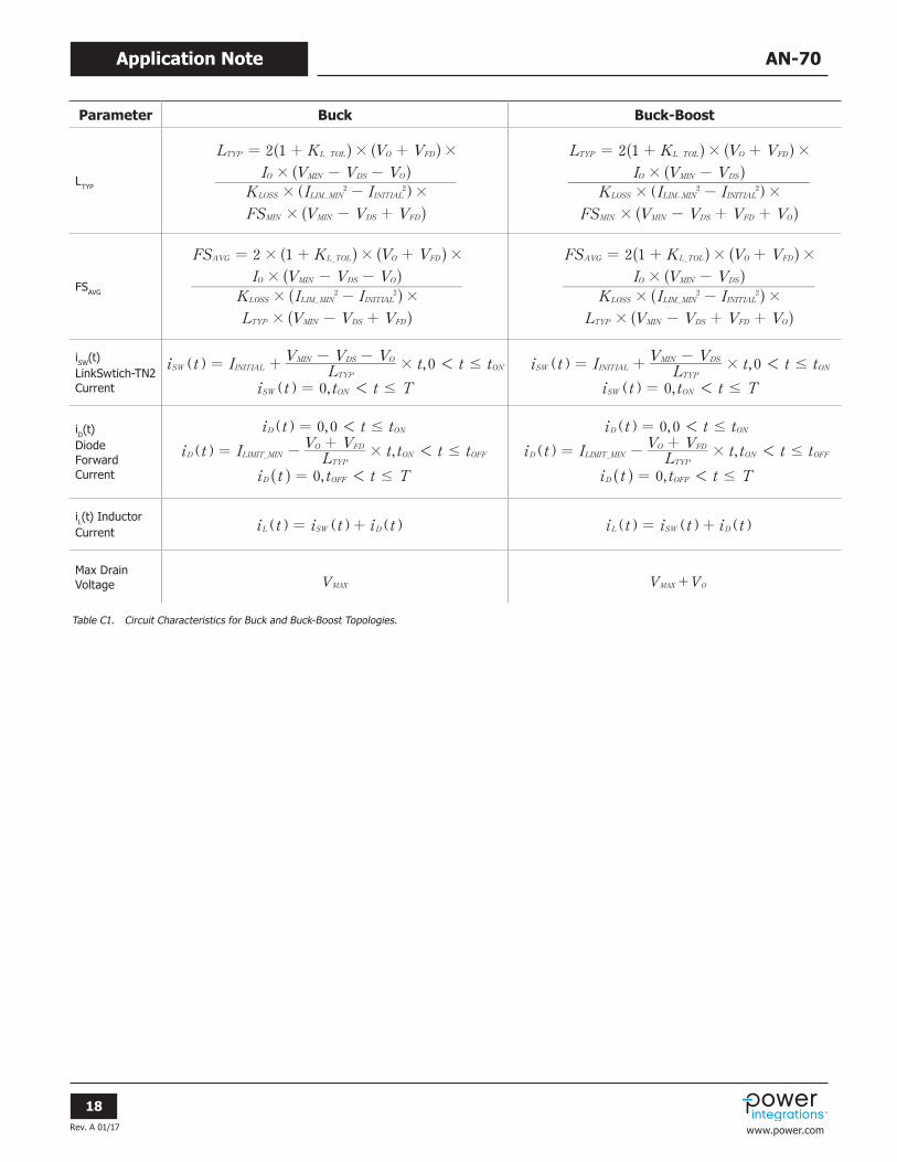
Rev. A 01/17
18
Application Note AN-70
www.power.com
Parameter Buck Buck-Boost
LTYP
FSAVG
iSW(t)LinkSwtich-TN2 Current
iD(t)Diode Forward Current
iL(t) Inductor Current
Max Drain Voltage
Table C1. Circuit Characteristics for Buck and Buck-Boost Topologies.
i t i t i tL SW D= +] ] ]g g g i t i t i tL SW D= +] ] ]g g g
VMAX V VMAX O+
,
,
i t I LV V V
t t t
i t t t T
0
0
SW INITIALTYP
MIN DS OON
SW ON
# 1
1
#
#
= +- -
=
]]
gg
,
,
i t I LV V
t t t
i t t t T
0
0
SW INITIALMIN DS
ON
SW ON
TYP# 1
1
#
#
= +-
=
]]
gg
K I I
L V V V
FS K V V
I V V V
2 1 _
LOSS LIM MIN INITIAL
TYP MIN DS FD
AVG L TOL O FD
O MIN DS O
2 2# #
#
# # #
#
-
- +
= + +
- -
-
^
^
^
^
^h
h
h
h
h
K I I
FS V V V
L K V V
I V V V
2 1
LOSS LIM MIN INITIAL
MIN MIN DS FD
TYP L TOL O FD
O MIN DS O
2 2# #
#
# #
#
-
- +
= + +
- -
-
-^
^
^
^
^h
h
h
h
h
,
,
,
i t t t
i t I LV V
t t t
i t
t
t t T
0 0
0
_
D ON
D LIMIT MINTYP
O FDON OFF
D OFF
#
1
1
1
#
#
#
=
= -+
=
]
^
]g
h
g ,
,
,
i t t t
i t I LV V
t t t
i t
t
t t T
0 0
0
_
D ON
D LIMIT MINTYP
O FDON OFF
D OFF
#
1
1
1
#
#
#
=
= -+
=
]
^
]g
h
g
K I I
FS V V V V
L K V V
I V V
2 1
LOSS LIM MIN INITIAL
MIN MIN DS FD O
TYP L TOL O FD
O MIN DS
2 2# #
#
# #
#
-
- + +
= + +
-
-
-^
^
^
^
^h
h
h
h
h
K I I
L V V V V
FS K V V
I V V
2 1 _
LOSS LIM MIN INITIAL
TYP MIN DS FD O
AVG L TOL O FD
O MIN DS
2 2# #
#
# #
#
-
- + +
= + +
-
-
^
^
^
^
^h
h
h
h
h
Rev. A 01/17
19
Application NoteAN-70
www.power.com
Appendix C ‒ Protection Feature for Flyback Applications
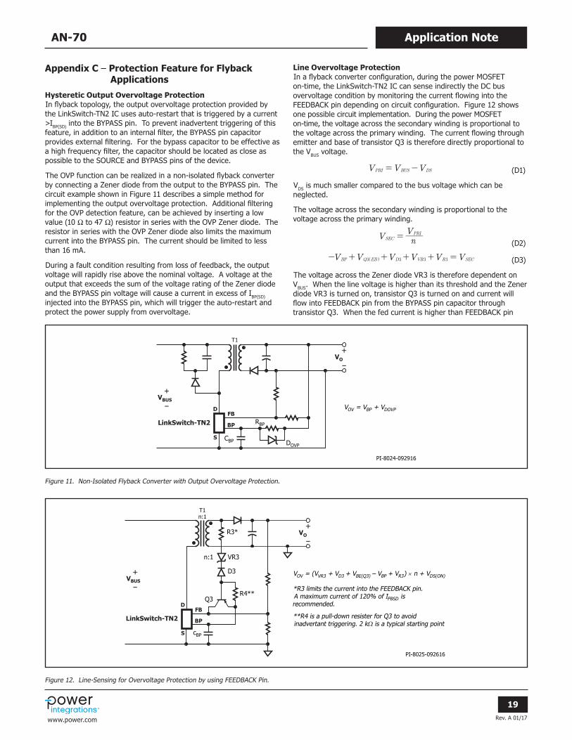
Hysteretic Output Overvoltage Protection In flyback topology, the output overvoltage protection provided by the LinkSwitch-TN2 IC uses auto-restart that is triggered by a current >IBP(SD) into the BYPASS pin. To prevent inadvertent triggering of this feature, in addition to an internal filter, the BYPASS pin capacitor provides external filtering. For the bypass capacitor to be effective as a high frequency filter, the capacitor should be located as close as possible to the SOURCE and BYPASS pins of the device.
The OVP function can be realized in a non-isolated flyback converter by connecting a Zener diode from the output to the BYPASS pin. The circuit example shown in Figure 11 describes a simple method for implementing the output overvoltage protection. Additional filtering for the OVP detection feature, can be achieved by inserting a low value (10 Ω to 47 Ω) resistor in series with the OVP Zener diode. The resistor in series with the OVP Zener diode also limits the maximum current into the BYPASS pin. The current should be limited to less than 16 mA.
During a fault condition resulting from loss of feedback, the output voltage will rapidly rise above the nominal voltage. A voltage at the output that exceeds the sum of the voltage rating of the Zener diode and the BYPASS pin voltage will cause a current in excess of IBP(SD) injected into the BYPASS pin, which will trigger the auto-restart and protect the power supply from overvoltage.
VO
VBUS
LinkSwitch-TN2
D
S
FB
BP
+
PI-8024-092916
T1
DOVP
RBP
CBP
VOV = VBP + VDOVP
+
VO
LinkSwitch-TN2
D
S
FB
BP
+
PI-8025-092616
VOV = (VVR3 + VD3 + VBE(Q3) – VBP + VR3) × n + VDS(ON)
*R3 limits the current into the FEEDBACK pin. A maximum current of 120% of IFBSD is recommended.
**R4 is a pull-down resister for Q3 to avoid inadvertant triggering. 2 kΩ is a typical starting point
R3*
VR3n:1
R4**
cBP
Q3
D3VBUS
+
T1n:1
Figure 11. Non-Isolated Flyback Converter with Output Overvoltage Protection.
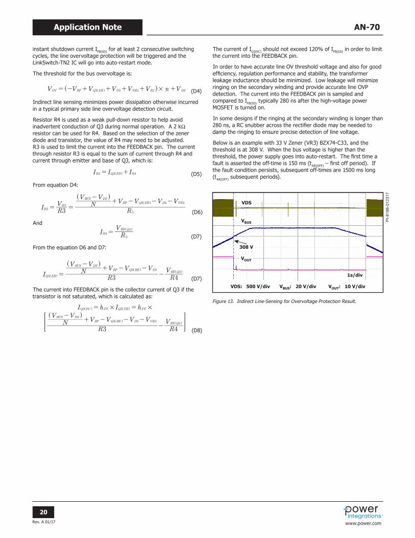
Figure 12. Line-Sensing for Overvoltage Protection by using FEEDBACK Pin.
Line Overvoltage Protection In a flyback converter configuration, during the power MOSFET on-time, the LinkSwitch-TN2 IC can sense indirectly the DC bus overvoltage condition by monitoring the current flowing into the FEEDBACK pin depending on circuit configuration. Figure 12 shows one possible circuit implementation. During the power MOSFET on-time, the voltage across the secondary winding is proportional to the voltage across the primary winding. The current flowing through emitter and base of transistor Q3 is therefore directly proportional to the VBUS voltage.
V V VPRI BUS DS= - (D1)
VDS is much smaller compared to the bus voltage which can be neglected.
The voltage across the secondary winding is proportional to the voltage across the primary winding.
V n
VSEC
PRI= (D2)
V V V V V VBP Q EB D VR R SEC3 3 3 3- + + + + =^ h (D3)
The voltage across the Zener diode VR3 is therefore dependent on VBUS. When the line voltage is higher than its threshold and the Zener diode VR3 is turned on, transistor Q3 is turned on and current will flow into FEEDBACK pin from the BYPASS pin capacitor through transistor Q3. When the fed current is higher than FEEDBACK pin
Rev. A 01/17
20
Application Note AN-70
www.power.com
Figure 13. Indirect Line-Sensing for Overvoltage Protection Result.
instant shutdown current IFB(SD) for at least 2 consecutive switching cycles, the line overvoltage protection will be triggered and the LinkSwitch-TN2 IC will go into auto-restart mode.
The threshold for the bus overvoltage is:
V V V V V V n VOV BP Q EB D VR R DS3 3 3 3 #= - + + + + +^ ^ hh (D4)
Indirect line sensing minimizes power dissipation otherwise incurred in a typical primary side line overvoltage detection circuit.
Resistor R4 is used as a weak pull-down resistor to help avoid inadvertent conduction of Q3 during normal operation. A 2 kΩ resistor can be used for R4. Based on the selection of the zener diode and transistor, the value of R4 may need to be adjusted.R3 is used to limit the current into the FEEDBACK pin. The current through resistor R3 is equal to the sum of current through R4 and current through emitter and base of Q3, which is:
I I IR Q EB R3 3 4= +^ h (D5)
From equation D4:
I R
VR
NV V
V V V V
3RR
VRBUS DS
BP Q EB D
33
3
3
3 3
= =
-+ - - -
^^
hh
(D6)
And
I R
VR
BE Q4
4
3=^ h
(D7)
From the equation D6 and D7:
I R
NV V
V V V
RV
3 4
BUS DSBP Q D
Q EB
BEBE Q
3
3 33=
-+ - -
-
^^
^ ^h
hh h
(D7)
The current into FEEDBACK pin is the collector current of Q3 if the transistor is not saturated, which is calculated as:
I h I h
RN
V VV V V V
RV
3 4
Q EC FE Q EB FE
BUS DSBP Q BE D VR
BE Q
3 3
3 3 33
# #= =-
+ - - --
^^
^
^
^h
h
h
h
h> H (D8)
The current of IQ3(EC) should not exceed 120% of IFB(SD) in order to limit the current into the FEEDBACK pin.
In order to have accurate line OV threshold voltage and also for good efficiency, regulation performance and stability, the transformer leakage inductance should be minimized. Low leakage will minimize ringing on the secondary winding and provide accurate line OVP detection. The current into the FEEDBACK pin is sampled and compared to IFB(SD) typically 280 ns after the high-voltage power MOSFET is turned on.
In some designs if the ringing at the secondary winding is longer than 280 ns, a RC snubber across the rectifier diode may be needed to damp the ringing to ensure precise detection of line voltage.
Below is an example with 33 V Zener (VR3) BZX74-C33, and the threshold is at 308 V. When the bus voltage is higher than the threshold, the power supply goes into auto-restart. The first time a fault is asserted the off-time is 150 ms (tAR(OFF) ‒ first off period). If the fault condition persists, subsequent off-times are 1500 ms long (tAR(OFF) subsequent periods).
PI-81
98-012
317
VDS
VDS: 500 V/div VBUS: 20 V/div VOUT: 10 V/div
VBUS
308 V
VOUT
1s/div


Revision Notes Date
A Initial Release. 01/17
For the latest updates, visit our website: www.power.comPower Integrations reserves the right to make changes to its products at any time to improve reliability or manufacturability. Power Integrations does not assume any liability arising from the use of any device or circuit described herein. POWER INTEGRATIONS MAKES NO WARRANTY HEREIN AND SPECIFICALLY DISCLAIMS ALL WARRANTIES INCLUDING, WITHOUT LIMITATION, THE IMPLIED WARRANTIES OF MERCHANTABILITY, FITNESS FOR A PARTICULAR PURPOSE, AND NON-INFRINGEMENT OF THIRD PARTY RIGHTS.
Patent InformationThe products and applications illustrated herein (including transformer construction and circuits external to the products) may be covered by one or more U.S. and foreign patents, or potentially by pending U.S. and foreign patent applications assigned to Power Integrations. A complete list of Power Integrations patents may be found at www.power.com. Power Integrations grants its customers a license under certain patent rights as set forth at http://www.power.com/ip.htm.
Life Support PolicyPOWER INTEGRATIONS PRODUCTS ARE NOT AUTHORIZED FOR USE AS CRITICAL COMPONENTS IN LIFE SUPPORT DEVICES OR SYSTEMS WITHOUT THE EXPRESS WRITTEN APPROVAL OF THE PRESIDENT OF POWER INTEGRATIONS. As used herein:
1. A Life support device or system is one which, (i) is intended for surgical implant into the body, or (ii) supports or sustains life, and (iii) whose failure to perform, when properly used in accordance with instructions for use, can be reasonably expected to result in significant injury or death to the user.
2. A critical component is any component of a life support device or system whose failure to perform can be reasonably expected to cause the failure of the life support device or system, or to affect its safety or effectiveness.
The PI logo, TOPSwitch, TinySwitch, SENZero, SCALE-iDriver, Qspeed, PeakSwitch, LYTSwitch, LinkZero, LinkSwitch, InnoSwitch, HiperTFS, HiperPFS, HiperLCS, DPA-Switch, CAPZero, Clampless, EcoSmart, E-Shield, Filterfuse, FluxLink, StakFET, PI Expert and PI FACTS are trademarks of Power Integrations, Inc. Other trademarks are property of their respective companies. ©2017, Power Integrations, Inc.
World Headquarters5245 Hellyer AvenueSan Jose, CA 95138, USAMain: +1-408-414-9200Customer Service:Phone: +1-408-414-9665Fax: +1-408-414-9765e-mail: [email protected]
China (Shanghai)Rm 2410, Charity Plaza, No. 88North Caoxi RoadShanghai, PRC 200030Phone: +86-21-6354-6323Fax: +86-21-6354-6325e-mail: [email protected]
China (Shenzhen)17/F, Hivac Building, No. 2, Keji Nan 8th Road, Nanshan District, Shenzhen, China, 518057Phone: +86-755-8672-8689Fax: +86-755-8672-8690e-mail: [email protected]
GermanyLindwurmstrasse 11480337 MunichGermanyPhone: +49-895-527-39110Fax: +49-895-527-39200e-mail: [email protected]
GermanyHellwegForum 159469 EnseGermany Tel: +49-2938-64-39990e-mail: igbt-driver.sales@ power.com
India#1, 14th Main RoadVasanthanagarBangalore-560052 IndiaPhone: +91-80-4113-8020Fax: +91-80-4113-8023e-mail: [email protected]
ItalyVia Milanese 20, 3rd. Fl.20099 Sesto San Giovanni (MI) ItalyPhone: +39-024-550-8701Fax: +39-028-928-6009e-mail: [email protected]
JapanKosei Dai-3 Bldg. 2-12-11, Shin-Yokohama, Kohoku-ku Yokohama-shi, Kanagawa 222-0033 JapanPhone: +81-45-471-1021Fax: +81-45-471-3717e-mail: [email protected]
KoreaRM 602, 6FLKorea City Air Terminal B/D, 159-6Samsung-Dong, Kangnam-Gu,Seoul, 135-728, KoreaPhone: +82-2-2016-6610Fax: +82-2-2016-6630e-mail: [email protected]
Singapore51 Newton Road#19-01/05 Goldhill PlazaSingapore, 308900Phone: +65-6358-2160Fax: +65-6358-2015e-mail: [email protected]
Taiwan5F, No. 318, Nei Hu Rd., Sec. 1Nei Hu Dist.Taipei 11493, Taiwan R.O.C.Phone: +886-2-2659-4570Fax: +886-2-2659-4550e-mail: [email protected]
UKBuilding 5, Suite 21The Westbrook CentreMilton RoadCambridge CB4 1YGPhone: +44 (0) 7823-557484e-mail: [email protected]
Power Integrations Worldwide Sales Support Locations