application characterization of igbts - c & h technology, inc
TRANSCRIPT

INT990
Application Characterization of IGBTs(HEXFRED® is a trademark of International Rectifier)
Topics Covered:
Gate drive for IGBTsSafe Operating AreaConduction lossesStatistical modelsSwitching lossesDevice selection and optimizationSpreadsheets to calculate power losses and junction temperatureThermal designHow to replace a power MOSFETParallelingHow to select devices for parallelingCurve fitting methods to derive model parameters
SCOPE:
This application note covers some of the major issues normally encountered in the design of an IGBT power conditioningcircuit. It is the companion to INT-983, "IGBT Characteristics," which covers the details of the device, rather than itsapplication.
I. GATE DRIVE REQUIREMENTS
A . Impact of the impedance of the gate drive circuit on switching losses
The gate drive circuit controls directly the MOSFET channelof the IGBT and, through the drain current of the MOSFET,the base current of its bipolar portion. Since the turn-oncharacteristics of an IGBT are determined, to a large extent,by its MOSFET portion, the turn-on losses will besignificantly affected by the gate drive impedance. Turn-offcharacteristics, on the other hand, are chiefly determined bythe minority carrier recombination mechanism, which isonly indirectly affected by the MOSFET turn-off. Anincrease in gate drive impedance prolongs the Miller effectand causes a delay in the current fall time that is similar to astorage time. This delay is emphasized in Figure 1 with theaddition of a 47W gate resistor. The impact of the gate driveimpedance on total switching losses depends on the basicdesign of the IGBT and its speed. The impact on turn-onlosses is appreciable for all IGBTs from InternationalRectifier, regardless of speed. The impact on turn-off lossesdepends on the speed of the device: the faster the IGBT thegreater its sensitivity to the gate drive impedance. In anyevent, additional gate drive impedance has a marginalimpact, i.e. the same amount of additional drive impedancewill have a lower effect if the gate drive impedance isalready high.
It follows that the total switching losses of Fast IGBT will be less affected by the characteristics of the gate drive circuit than theUltrafast IGBTs. These last ones are more sensitive to it and stand to benefit the most from a low impedance gate drive. Thespecific dependence of the switching energy on gate drive resistance is shown in the data sheet.
IC
VGE
VCE
VCE : 100V/div.IC : 5A/div.VGE : 10V/div., 0.1 µµs/div.
Figure 1. Turn-off waveform of an IRGBC40F witha 47W gate resistor. Notice the turn-off delay ofthe current waveform during the Miller effect.

INT990
B. Impact of the gate drive impedance on noise sensitivity
As explained in INT-936, in a MOSGated transistor, any dv/dt thatappears on the collector/drain iscoupled to the gate through acapacitive divider consisting of theMiller capacitance and the gate-to-source/emitter capacitance. If the gateis not solidly clamped to thesource/emitter, a large enough dv/dtwill take the gate voltage beyond itsthreshold and the transistor willconduct. As it goes into conduction itclamps the dv/dt that is causing it toconduct so that the gate voltagenever goes much beyond itsthreshold. The end result is a limitedamount of "shoot-through" current,with an increase in power dissipation.To reduce noise sensitivity and therisk of this dv/dt-induced turn-on,the gate must be shorted to theemitter through a very low impedance. Frequently a negative gate bias is used to improve noise immunity. An effectivealternative is to design a layout that minimizes the inductance of the gate charge/discharge loops with parallel tracks or twistedwires for the gate drive.
This can be as effective in taking care of this problem as the negative bias, eliminating the need for isolated negative supplies.In many cases the effects of a contained amount of dv/dt induced turn-on, i.e. a small increase in power dissipation, can be anappealing alternative to the added complexity of the negative gate bias.
C. Impact of gate drive impedance on "dynamic latching"
Some manufacturers suggest the use ofsignificant amounts of gate resistance to reducethe possibility of "dynamic latch-up" (see INT-983, Section I.d), particularly when short circuitcurrents have to be switched off. This increasesthe switching energy and the sensitivity to dv/dtinduced turn-on. Under these conditions anegative gate bias may be required.
Although IGBTs from International Rectifierwill not latch even with no gate resistance,there may be practical reasons to add them,mainly to reduce the current spike at turn-ondue to reverse recovery of the diode and reduceringing.
This resistance can be safely bypassed with ananti-parallel diode to reduce the turn-off lossesand the amount of dv/dt induced turn-on, asexplained in INT-978, Section 3.b. For mostapplications, the circuit shown in Figure 2provides a simple, low cost, high performancesolution to the gate drive requirements of mostapplications.
15V
0V
15V
0V
+15V 8 NC
9 VDD
10 HIN
11 SD
12 LIN
13 VSS
14 NC
7HO
6VB
5VS
4NC
3VCC
2COM
1LO
IR2110
V+
Figure 2. The IR2110 provides a simple, high performance, low costsolution to the problem of driving a Half-Bridge.
VCC
IN
ERR
VSS
VB
OUT
CS
VS
C3
C1
C5 RS1
IR21
25
VCC
IN
ERR
VSS
OUT
CS
VS
C4
C2
C6 RS2
IR21
21
VCC
T1
C7
C8
V+
V-
IN1
IN2
VCC
D1
Figure 3. Short circuit protection performed withMOS gate driver ICs

INT990
D. Using gate voltage to improve short circuit capability
The gate terminal can be advantageously used to control the short-circuit withstand capability of the IGBT. A lower gate drivevoltage reduces the collector current and the power dissipation during short circuit, at the expenses of a higher conduction drop.As an alternative, simple circuits can be implemented to reduce the gate voltage within 1-3 ms from the inception of the shortcircuit. INT-984 provides an example of how this function can be performed.
MOS-Gate Driver integrated circuits are available to perform the current limiting and short circuit protection function by meansof the gate voltage. One such example is shown in Figure 3.
E. Contribution of "common emitter inductance" to the impedance of the gate drive circuit
The "common emitter inductance" is the inductance that is common to the collector circuit and the gate circuit (Figure 4a). Thisinductance establishes a feedback from the collector circuit to the gate circuit that is proportional to LdiC/dt. The voltagedeveloped across this inductance subtracts from the applied gate voltage during the turn-on transient and adds to it during turn-off. In so doing, it slows down the switching.
This phenomenon is similar to the Miller effect, except that it is proportional to the di/dt of the collector current rather than thedv/dt of its voltage. In both cases the feedback is proportional to the transconductance of the IGBT, which is much larger thanthat of a MOSFET of the same die size. A diC/dt of 0.5A/ns is quite common in IGBT circuits and voltages in the order of 10Vcould be expected in 20 nH of common emitter inductance, except that the feedback mechanism slows down the turn-on processand limits the dic/dt.
No additional common emitter inductance should be added to what is already in the package. Separate wires to the emitter pinshould be provided for the emitter and the gate return, as shown in Figure 4b. The gate lead and the gate return lead should betwisted or run on parallel tracks to minimize inductance in the gate drive path. This improves immunity to dv/dt induced turn-onand reduces ringing in the gate.
F. Gate charge vs. input capacitance
The difference between gate capacitance and gate charge is covered in INT-944. Designers that are familiar with the limitedusefulness of the input capacitance concept can safely skip this section.
Input capacitance is frequently used for two purposes:
• as a figure of merit of switching performance;• as a reference point to design a gate drive circuit.
Za
LOAD
SUPPLY
LOAD CURRENT
COMMON EMITTER INDUCTANCE
PACKAGEINDUCTANCE
GATE DRIVECURRENT
Figure 4a. " Common Emitter Inductance" is the inductance thatis common to the collector current and the gate drive current
Figure 4b. " Common Emitter Inductance" can beeliminated by running separate wires to the emitter pin, onefor the emitter, the other for the gate drive return.
Za
LOAD
SUPPLY
LOAD CURRENT
TWISTED

INT990
On both counts, the use of data sheet capacitance valuesgives results that are wrong or misleading.
As shown in Figure 5, IGBT capacitances changesignificantly with collector voltage to the point that nocapacitance number is, in itself, meaningful unless a voltageis associated with it.
Even disregarding the voltage dependence, input capacitanceis not a good figure of merit of switching performance,neither for MOSFETs, nor for IGBTs. As far as MOSFETsgo, a device with lower input capacitance can be slower thanone with higher input capacitance, depending on threshold,transconductance and total gate charge (see Figure 6 of INT-944). A conspicuous example of this is the fact that logiclevel devices are faster than their standard gate counterparts,in spite of a larger input capacitance [1].
In the specific case of IGBTs, which are minority carrierdevices, the switching behavior is dominated by injectionand recombination phenomena and only the turn-onbehavior is affected by gate drive conditions in a significantway.
As a guideline to design the gate drive circuit, the input capacitance underestimates the gate drive requirements. Normally, thecharge required by the gate for one switching operation corresponds to an input capacitance that is two to three times largerthan the data sheet value. As explained in INT-944, this is due to the Miller component of the input capacitance.
Thus, gate drive circuits designed on the basis of input capacitance are generally inadequate and result in poor switchingoperation and noise susceptibility. The sizing of the gate drive circuit is more appropriately done using the gate charge specifiedin the data sheet.
II. SWITCHING TRAJECTORIES AND SAFE OPERATING AREACONSIDERATIONS
Minority carrier devices, when subjected to high levels of voltage and current, can experience uneven current distributionswithin the die that, taken beyond safe limits, can cause device failure. The current distribution takes different forms, dependingon the sign of the di/dt associated with it. Hence, the Safe Operating Area curve, which was devised as a convenientrepresentation of this limitation, is frequently differentiated into "Forward Biased SOA" and "Reverse-Biased SOA".
The Forward Biased SOA curve applies to linear operation in Class A or Class B or during short circuit, which can beconsidered an extreme case of Class B operation. Thermal limitations for pulsed operation are frequently included in this curve,even though the Transient Thermal Response curve provides this same information in a more comprehensive and accurate way.Due to the limited use of these devices in linear operation, the FBSOA curve has been omitted from the data sheet. The ReverseBiased SOA applies when switching off a clamped inductive load, including the turn-off from a short circuit condition.
Figure 6 shows the importance of the Reverse Biased SOA. During the turn off of a clamped inductive load, the voltage acrossthe transistor goes from the low value of VCE(sat) to the full supply voltage while the collector current stays constant. After thecollector voltage exceeds the supply voltage by a diode drop, the diode starts to conduct, thereby taking over the inductor currentfrom the transistor. Thus the trajectory of the operating point moves along a constant current line until it intercepts the supplyvoltage, at which point a voltage overshoot normally occurs, whose magnitude depends on the amount of stray inductance LS
and the turn-off speed. A more detailed explanation of the switching trajectories can be found in Ref. [2].
It will be appreciated that, for a safe commutation of the load current, the entire trajectory must lay within the turn-off SOA andthat any limitation to the SOA will translate into a limitation of turn-off capability of inductive loads. Load-shaping snubbershave been used in conjunction with bipolar transistors to lower the trajectory below the second breakdown limit.
Cies
Coes
Cres
VGE = 0V f = 1MHzCies = Cge + Cgc . Cce SHORTEDCres = CgeCoes = Cce + Cgc
0
1500
3000
4500
6000
7500
100 101
VCE, COLLECTOR-TO-EMITTER VOLTAGE (V)
CA
PA
CIT
AN
CE
(pF
)
Figure 5. Typical capacitance vs VCE, IRGPC50U.The variation of Cres and Cies with collector voltagemakes the concept of capacitance virtually useless.

INT990
Due to the wide base and, hence, low gain of its bipolar portion, the second breakdown of International Rectifier's IGBTs occurat current and voltage levels that are significantly higher than what is normally encountered in a practical application, as shownin the data sheets. Notice that the values therein contained apply at 125°C and that load-shaping snubbers are not necessary, aslong as the switching trajectory is confined within the turn-off SOA. During an inductive turn-off, a bipolar-mode device canundergo a partial loss of blocking capability, similar in many respects to second breakdown. This phenomenon is generallyexplained as being due to excessive concentration of minority carriers in the base region [3], rather than lateral thermalinstability. For the IGBTs available from International Rectifier at the time of writing, this phenomenon occurs well beyond theSOA limits published in the data sheet. In addition to load shaping, snubbers can be used to limit overshoots and/or reduceEMI. This function is not related to SOA and is covered in more detail in INT-936.
III. CONDUCTION LOSSES
At any given time, the energy dissipated in the IGBT can be obtained with the following expression:
( ) ( )E V i i t dtCE
t= ∫
0
where t is the length of the pulse. Power is obtained by multiplying energy by frequency, if applicable. When the transistor is offi(t) » 0 and losses are negligible. Unfortunately, no simple expression can be found for the voltage and current functions duringa switching transient. Hence, for analytical expediency, we resort to a somewhat artificial distinction between conduction andswitching losses.
We define conduction losses the losses that occur between the end of the turn-on interval and the beginning of the turn-offinterval, as defined for the switching losses characterization. Since the turn-on energy is measured from 5% of the test currentto 5% of the test voltage and the turn-off energy is measured starting from 5% of the test voltage, conduction losses occur whenthe voltage across the IGBT is less than 5% of the test, or supply, voltage (see INT-983, Section 8.5). The function VCE(i) in theformula above expresses the conduction behavior of the IGBT. International Rectifier characterizes the conduction losses in thefollowing ways:
• with tabular information in the data sheet;• with graphs in the data sheet;• with the model Parameters of INT-MODEL.
Figure 6a. Typical clamped inductive load
IL
LS
IL
IC
VCE(sat) @ IL
VC
VO
Figure 6b. During a turn-off transient, the trajectory of theoperating point traverses the SOA curve. Secondbreakdown would place limits to the free evolution of thetrajectory.

INT990
A. Calculating the voltage drop from data sheet parameters
The tabular information in the data sheet provides a few limit points that, with the help of the graphs, can be used to generatethe information necessary to calculate the conduction losses. To obtain the max voltage drop at any current and temperature,from the data sheet supplied values, a two step procedure can be followed. First a typical value is obtained by interpolating acurve in Figure 5 of the data sheet at the desired current level. Then, to obtain a maximum value, the voltage drop read fromthis curve at the appropriate junction temperature is multiplied by the ratio between maximum and typical from the Table ofElectrical Characteristics. If the current waveform is not constant during the conduction interval, it should be broken up intosmaller intervals, calculating the losses for each sub-interval and summing the results, rather than averaging or taking its RMSvalue. An appealing alternative, for those cases where the current waveform has a simple mathematical expression, e.g.sinusoidal or triangular or trapezoidal, is to calculate the conduction losses with the integral above, with the help of theconduction model.
B. Conduction model
The solution of the integral requires a mathematical expression for the current waveform and one for the voltage drop. Theexpression shown below for the voltage drop as a function of current was found to be more than satisfactory for the generalaccuracy that is expected from these calculations.
VCB = Vt + a Ib
Information on the accuracy of the model and how it was derived is contained in Appendix 1.The specific parameters for the families of IGBTs from International Rectifier can be found in INT-MODEL. The purpose of thismodel, as well as the one presented in Section IV.B is to accurately predict the junction temperature of the IGBT in order to getthe most out of the device. They differ from the common SPICE model in significant ways:∗ they are representative of a population of devices, characterized by averages and sigmas, rather than an undefined "typical"
device;∗ they model electrical magnitudes that are time-independent, hence increments, and convergence are not an issue;∗ temperature is an integral part of the model, not an after thought;∗ the models are integrateable to calculate averages or losses in complex modulation schemes;∗ the model is suited to provide aggregate values, like average power, average temperature, average peak reverse recovery.These models do not provide information on the details of collector or gate waveforms. It should be kept in mind, however, thatthese waveforms are determined by circuit parasitics that cannot be modeled without breadboard characterization.
CURRENTWAVEFORM
MATHEMATICALEXPRESSION
( )E V i i t dt V i V ai E V i t ai t dtCE CE tb
tb= = + = +
+∫∫ ( ) ( ) , ( ) ( ) ( ) 1
I
ton0 ( )i t I=( ) ( )E IV aI dt IV aI ttb
ton
tb
on= +
= +
+ +∫ 1
0
1
I2
t10
I1( ) ( )i t I I I
t
t= + −1 2 1
1( ) ( ) ( ) ( ) ( ) ( )
( )E V II I
ta I
I I
tt dt V
I It
I I
I I
at
bT
t b
t
b b
= +−
+ +
−
=
++
−− +∫
+ + +
12 1
10
1
12 1
1
12 1
12
21
2
2 1
12 2
I
t10( )i t I
t
t=
1( ) ( )E V I t aI t dt
IV aI
b
btb b
t
tb= +
= +
+
+ +∫ 0 01 1 0
0
1
02
3
2
sin sinω ωω
π2
Γ+ 22
Γ
I0
π0
( )i t I t= 0 sin ω ( ) ( )E V I t aI t dtI
V aI
b
btb b
t
tb= +
= +
+
+ +∫ 0 01 1 0
0
1
02
3
2
sin sinω ωω
π2
Γ+ 22
Γ
I0
πα
( )i t I t= 0 sin ω
( ) ( )
for EI
V aI
b
b
otherwise EI
V aI d
tb
tb b
α π2 ω
π2
Γ
Γ
ωα α α
α
π
= +
+
+
= + +
+∫
00
00
1
2
23
2
1 cos sin
Table I. Conduction Energy for Simple WaveformsTable I shows the expressions to calculate conduction energy for five simple current waveforms, assuming that the conductionbehavior is accurately expressed by the model presented.

INT990
As shown in Sections V and VI, this model, as well as the companion switching model that will be described in the next Section,is extremely useful in performing comparative evaluations for device optimization. Section VI shows how it can be used tosimplify and automate the calculation of junction temperature for any operating condition.
IV. LOSSES IN HARD SWITCHING
Like conduction losses, "hard switching" operation is characterized in the following ways:
• with tabular information in the data sheet;• with graphs in the data sheet;• with the model parameters of Table INT-MODEL.
As explained in INT-983, Section 8.5, the Switching Energy reported in the data sheet makes specific reference to a test circuitthat simulates a clamped inductive load operated with an ideal diode. Hence, it does not include the losses in the IGBT when, inturning on, it carries the full load current, plus the reverse recovery current of the freewheeling diode.
It follows that, to obtain the total turn-on losses or the total switching losses, two components have to be calculated:
• turn-on or total losses with an ideal diode• the additional turn-on losses in the IGBT due to the reverse recovery of the freewheeling diode.
The following sections show how to calculate these two components. It should be kept in mind that active devices in flybackconverters do not normally have turn-on losses, nor are they subject to recovery transients. The same is true for those bridgecircuits where the output voltage and duty cycle is controlled by phase shifting the output of one leg with respect to the other,both being 50% duty cycle.
A. Calculation of switching losses with an ideal diode from data sheet information
Total switching losses with an ideal diode for any given current and temperature can be obtained from data sheet informationfollowing a three step procedure, similar to the one for obtaining the on-state voltage drop.
First a typical value is obtained, by interpolating a curve in Figure 10 of the data sheet for the desired current. From this typicalvalue a maximum value can be obtained by multiplying the typical by the ratio between maximum and typical that is in the Tableof Switching Characteristics.
Finally, since the switching energy is proportional to voltage, the result is scaled by the ratio of the actual circuit voltage to thetest voltage (normally 80% of device rated voltage).
An additional correction may be necessary to account for the gate resistor. This can be done with the help of Figure 9 of the datasheet.
B. Calculation of switching losses with an ideal diode from switching model
A simpler alternative to the method outlined below is to make use of the simple model shown in Table III, together with thespecific parameters for the three families of IGBTs from International Rectifier. Losses calculated with these parameters assumethe following:
• supply voltages equal to 80% of rated V(BR)CES.• a gate drive circuit similar to the one in the data sheet.• ideal diode.
The results should be scaled linearly for the appropriate supply voltage and should be scaled according to Figure 9 of the datasheet to take into account a different gate drive impedance.

INT990
C. Contribution of the diode reverse recovery
In a typical clamped inductive load in continuous current mode, the turn-on of a switch causes a reverse recovery in thefreewheeling diode and a large current spike in the device that is being turned on (Figure 7). This increases the turn-on losses inthe IGBT with respect to the calculations of the previous sections and data sheet characterization. The forward recovery of thediode, on the other hand, has a secondary impact on the turn-off losses and will not be analyzed here.
No simple expression can be provided for these additional losses, as they depend on a number of factors: turn-on speed di/dt,stray inductance and diode characteristics. Several have been proposed, based on simplifying assumptions. The followingassumes that the voltage across the diode stays close to 0V during the length of ta, rising to the supply voltage during tb.
E VII
It
I
It
V I t Q Q
Lrr
La
rr
Lb
L a a b
= + +
= + +
[( ) ]
( )
11
2
1
4
1
2
where V and IL are supply voltage and load current, Irr is the peak reverse recovery current, ta and tb are the two components oftrr and Qa and Qb the charges associated with them. The first two terms represent the losses during ta, one due to the load current,the other due to the reverse recovery current. The third term represents the losses during tb, which are partly in the IGBT, partlyin the diode.
V. TRADE-OFF BETWEEN CONDUCTION AND SWITCHING LOSSES:DEVICE OPTIMIZATION
To compare different devices or technologies, silicon designers often resort to curves of voltage drop vs. current density likethose shown in Figure 8. These curves ignore the dynamic behavior of the device and, since in a typical Switchmode applicationa significant portion of the temperature rise is due to the switching losses, they are not useful in the device selection.
D1
V+
LOADCURRENT
D2
IC
IGBT1
IGBT2
REVERSERECOVERYCURRENT
LOAD PLUSREVERSE RECOVERYCURRENT
Figure 7a. Typical clamped inductive load showingstray circuit inductances. Load current was flowingin D1 previous to IGBT2 turning on. At turn-onIGBT2 takes over load current and reverserecovery current of D1
IC
VCE
VCE : 100V/div.IC : 5A/div., 0.1 µµs/div.
Figure 7b. Turn-on current in IGBT2.

INT990
Furthermore, it is frequently inferred, from those curves, that atechnology is superior if it is capable of operating at highercurrent densities. In a specific application, operation at highercurrent densities means smaller die sizes and, consequently,higher thermal resistances. If total losses stay the same, thisimplies higher operating junction temperature, with all itsnegative connotations.
It follows that, for a given thermal design, operation at highercurrent densities will be advantageous only if the higher thermalresistance is compensated by lower total losses.
To quantify these considerations a simple method has beendeveloped comparing different power devices in a typicalSwitchmode environment. This method takes all critical aspectsinto account: thermal constraints, conduction and switchinglosses.
The popular half-bridge operated with a clamped inductive loadwas chosen as the benchmark circuit to compare the Performanceof different IGBTs. Operating conditions are listed in Figure 9.None of the operating conditions are critical and they can all bechanged asnecessary. Flyback or resonant circuits could be used in place ofthe half-bridge to obtain results that are specifically tailored to agiven application.
This figure shows in a clear and concise way towhat extent higher switching frequencies impactthe current output of the pair.
It also provides a simple way of selecting theoptimum device for the application, which is theone that gives the highest output current at thefrequency of Operation.
Once the thermal constraints are properly factoredinto the operating conditions, the graph carriesimportant application information. In a motorcontrol, the RMS component of the fundamentalis directly related to torque.
In a power supply, on the other hand, the totalRMS content of the square wave contributes topower. The ratio between the two is 1.11.Although the graph shown in Figure 9 can begenerated with a relatively simple test circuit, wehave made use of the model presented in theprevious sections and of a spreadsheet like the one shown in Figure 10. Starting from the top, the IGBT model parameters areentered first, as appropriate for the junction temperature at which the performance is being evaluated.
Next the diode model is entered, which will be used to calculate the component of turn-on losses in the IGBT due to the reverserecovery of the diode. The conduction model for the diode can also be entered for completeness and to calculate its conductionlosses. This will not affect the losses in the IGBT but could provide useful information related to the total losses, efficiency, etc.
The reference voltage for the switching loss model (normally 80% of device rated voltage) is entered next, followed by the actualoperating voltage that, for a rectified 220V line, would be approximately 360V. Finally the thermal information is entered in theform of thermal resistance and ambient temperature, from which the allowable Power dissipation is calculated.
APPX DIE SIZE: 45mm2
1000C
TYPICAL VALUES
THYRISTOR:25RIA
1000C
IGBT: IRGPC50F
POWER MOSFET: IRF450
100
10
10 0.5 1.0 1.5 2.0
BUX98
2.5 3.0 3.5
0.066
0.22
0.66
2.22
VOLTAGE DROP (V)
CU
RR
EN
T (
A)
CU
RR
EN
T D
EN
SIT
Y A
/mm
2
Figure 8. Conduction characteristics for devicesof similar die size implemented in differenttechnologies.
IRGP50S
IRCPC50F
IRGPC50U
DUTY CYCLE : 50%
POWER DESITY : 1W/mm 2
TJ = 1250CIDEAL DIODEGATE DRIVE : AS SPECIFIED
360V
0.1 1 10 100
5
10
15
20
25
30
35
FREQUENCY, kHz
RM
S C
UR
RE
NT
- A
Figure 9. RMS current vs. frequency for a Half Bridge with twoIGBTs of same die size, same package, different speed, operatedin the conditions indicated in the inset.

INT990
The value "Current for balanced losses" is the current at which the conduction losses equal the switching losses for the specificthermal operating conditions. The corresponding frequency is shown at the bottom of the first column under "frequency, idealdiode". These values are calculated by means of a "solve for" function in the spreadsheet and are accurate to the numberindicated on the right of the current value. The rest of the spreadsheet performs the calculations of losses for different levels ofcurrent. Losses are broken down into two classes: conduction and switching. The formulas in the spreadsheet are described inthe next Section. All the losses are summarized at the bottom.
These values are used to generate the Current vs Frequency graph that is reported in each data sheet as Figure 1. If the diode isco-packaged with the IGBT its losses cannot be dissociated from the losses in the main switching device. In this case the thermalinformation and allowable power dissipation should be for the combination of both devices. Losses should include conductionand switching losses of both devices and the formulas should be modified accordingly.
Part Number:
IGBT MODEL Tj = 125
Conduction model: Vt = 0.86 a = 0.1834 b = 0.6999Turn-on model, ideal diode h = 0.0028 k = 1.6741Turn-off model: m = 0.018 n = 1.2486
DIODE MODEL Tj = 125
Conduction model: Vt = 1.00 a = 0.040 b = 1.000Switching model: Peak Irr/If =
1.00ta = 0.035 tb = 0.030µs
Switching parameters at 480 VOperating voltage: 360 VThermal resistance j-c 0.77 K/WThermal resistance c-s 0.24 K/WThermal resistance s-a 1.5 K/WAllowable powerdissipation
27.89 ^Ta =55
Current for balancedlosses
13.85 1E-05
Peak Current A 13.85 8 10 15 17.5 19.5
CONDUCTIONVoltage drop V 2.01 1.65 1.78 2.08 2.22 2.33Losses (50% duty cycle) W 13.94 6.58 8.89 15.6 19.42 22.68
SWITCHING LOSSESTurn-on, ideal diode mJ 0.1685 0.0673 0.0977 0.1927 0.2494 0.299IGBT losses due to diode mJ 0.2991 0.1728 0.216 0.324 0.378 0.4212Turn-off losses mJ 0.3595 0.1812 0.2394 0.3972 0.4815 0.5512Diode, switching losses mJ 0.0374 0.0216 0.027 0.405 0.0473 0.0527
SUMMARY:Conduction losses W 13.94 6.58 8.89 15.6 19.42 22.68Sw. losses, ideal diode mJ 0.53 0.25 0.34 0.59 0.73 0.85Pole RMS Current (fund.) A 12.46 7.200 9.000 13.5 15.75 17.55Frequency, ideal diode kHz 26.41 85.74 56.33 20.82 11.58 6.12Sw. losses, real diode mJ 0.83 0.42 0.55 0.91 1.11 1.27Frequency, real diode kHz 16.86 50.57 34.34 13.44 7.64 4.09
Figure 10. Spreadsheet to calculate Output current vs. Frequency

INT990
Figure 11. Analysis of the operating conditions of an IGBT in a clamped inductive load.
Part Number: IRGPC50U
THERMAL OPERATING CONDITIONSAmbient temperature °C 60.0Thermal resistance j-to-c °C/W 0.640Thermal resistance c-to-s °C/W 0.240Thermal resistance s-to-a °C/W 1.400
Allowable current Junction Temperatureat stated Tj for state current
Power dissipation W 28.5 29.16Junction temperature °C 125 * 126.50
IGBT MODELVt, Vt1, Vt2 V 0.8000 0.7958 1.0994 -2.40E-03a, a1, a2 Ohm 0.1120 0.1136 0.2021 -7.00E-04b, b1, b2 0.7117 0.7085 0.4656 1.92E-03h, h1, h2 mJ/A 0.0038 0.0037 0.0045 -6.10E-06k, k1, k2 1.6376 1.6399 1.6162 1.87E-04m, m1, m2 mJ/A 0.0128 0.0155 -0.0114 2.13E-04n, n1, n2 1.3382 1.336 1.9457 -4.82E-03Reference Voltage V 480 480
DIODE MODELVt 0.8 0.8 a, b 0.04 1 0.04 1Ratio Irr/If 1 1ta, tb µS 0.04 0.03 0.04
ELECTRICAL OPERATING CONDITIONS RECT. WAVEFRM, CLAMPED IND. LOADSwitching voltage V 360 360 Operating frequency kHz 40 40 Duty cycle 0.45 0.45Peak current A 9.82 9.82Voltage drop at peak current V 1.37 1.37Conduction losses W 6.05 6.05Turn-on losses W 4.76 4.76Correction factor for gate resistance 1.00 1.00Corrected turn-on losses W 4.76 4.76Turn-off losses W 8.14 9.87Correction factor for gate resistance W 1.00 1.00Corrected turn-off losses 8.14 9.87Turn-on losses due to diode recovery W 9.55 8.48Total losses W 28.50 29.16Junction temperature °C 126.49
RMS current, fundamental A 8.84 15.6 RMS current, total A 9.82 9.82 Output voltage, RMS funda mental V 162.000 162.00 Output power, fundamental kVA 1.59 1.59 Output power, total kVA 1.77 1.77 * Data entered

INT990
VI. THE ANALYSIS: METHODS TO CALCULATE JUNCTIONTEMPERATURE AND POWER DISSIPATION FOR A GIVEN OPERATINGCONDITION.
In the previous section we have developed an application related tool to compare the performance of different devices overtemperature and frequency. In this section we present a different tool, aimed at analyzing the operating conditions of the powerdevices, particularly its junction temperature, in a specific application environment.
Since temperature affects conduction and switching losses which, in turn, affect temperature, a direct mathematical solution isnot possible. However, the models introduced in Sections III and IV, applied iteratively, permit the characterization of a givenoperating condition with relative ease.
Figure 11 shows an example of such a spreadsheet. It provides junction temperature for a given a value of load current and agiven operating environment. It also provides a comprehensive analysis of the losses and temperatures in the thermal system.
This spreadsheet is quite general and applicable to any Switchmode conditioner. It is customized to our application, by enteringin the appropriate cells the expressions for power losses that characterize its operation.
In this example they represent a clamped inductive load, typically a Buck converter of Dual Forward. Equivalent spreadsheets formotor drives and UPS would look similar, while containing different formulas to reflect a different relationship between voltage,current, modulation and output power.
A spreadsheet has several advantages over other circuit analysis software:
• can be easily customized for specific applications without special programming expertise;• all the operating conditions that are important to the designer are summarized in less than half a page;• energy, power, peak and average currents and voltages are calculated and displayed, as opposed to waveforms on
nanosecond scales;• it is guaranteed to converge and provides a result in a fraction of a second• it allows true real-time interactive design: the impact of a change in voltage or current or frequency or heatsink is
assessed in a fraction of a second without printing stacks of waveforms.
The spreadsheet is divided in the three sections described below.
Input, output and gate drive conditions
All the parameters marked with an "X", like supply voltage, frequency, duty cycle, line current and turn-on gate resistor, shouldbe entered, the others are calculated from the data supplied. Within reasonable limits, the gate resistor at turn-off is not asimportant, as the turn-off mechanism of an IGBT is mostly dictated by minority carrier recombination
Thermal operating conditions
Ambient temperature and thermal resistances must be entered. Junction temperature is calculated from the losses listed in the lastbox of the spreadsheet. Junction temperature is used to calculate the device parameters which, in turn, are used to calculate thelosses.
This is the fundamental iteration process that yields the operating junction temperature.The thermal calculations would be somewhat different, depending on whether the inverter is implemented with discrete devices,co-packaged IGBT-diodes or modules.
Fig. 11 applies to discrete devices sharing the same heatsink with additional heat sources. The junction temperature is calculatedfor IGBTs and diodes.
For power modules this box would be modified to take into consideration the fact that the IGBTs and diodes contribute both toraise the base temperature of the module. Except for the modules which are already isolated, discrete and co-packaged devices areassumed to be isolated from the heatsink. The thermal resistance of the insulating interface is entered in this box.IGBT and diode model parameters

INT990
The third box contains the IGBT model parameters for the specific device, as explained in Section III.B, IV.B and XI. Theseparameters are used to calculate the voltage drop and switching energy as a function of current at the specific temperatureindicated in the previous box. They are automatically fetched from a table that is part of the spreadsheet but not shown in Fig.11.
The diode conduction model is shown in the right-hand side of this box. Recovery parameters are calculated here from the turn-on di/dt of the IGBT which is, in turn, a function of the turn-on gate resistor entered in the first box. The recovery parameters areimportant to calculate the turn-on losses of the IGBT and the switching losses of the diode.
Power losses
The fourth box lists the components of power losses and junction temperature for one IGBT and the freewheeling diode.
Although the most important information provided by the spreadsheet is the operating junction temperature of the IGBT and ofthe diode, the additional information provided in the last box is also very useful in optimizing the choice of the power devices.The following observations can be used as examples:
♦ If the switching losses are much larger than the conduction losses, a faster IGBT is desirable. If none is available, it may beadvisable to lower the junction temperature to avoid the risk of thermal run-away due to the fact that turn-off losses increasesignificantly with temperature. This can be done by improving the thermal system, e.g. by increasing the size of the heatsink orisolating the heatsink rather than the IGBT.
The risk of thermal runaway can be easily checked with the help of the spreadsheets by increasing ambient temperature by a fewdegrees. If junction temperature increases by more than the increase in ambient temperature, there is cause for concern.
♦ If, on the other hand, conduction losses are the dominant component, a slower device may reduce the overall losses andoperate at a lower junction temperature.
♦ If a large share of the IGBT losses are due to the diode recovery, a faster diode should be used or faster turn-on of the IGBT.This increases the turn-on spike, but reduces the turn-on losses. ♦ In a well balanced thermal design the case temperature of the active devices is between one-half and three-fourths thetemperature rise between ambient and junction. If it lower than that, the heatsink could be reduced. If it is higher, it may be toosmall. ♦ When a suitable device cannot be found, designers frequently turn to paralleling, a method that has proven quite successfulwith power MOSFETs. It is somewhat less successful with IGBTs because their dominant losses are switching and switchinglosses do not decrease with paralleling. They may, in fact, increase, if the gate drive is not adequate. The generally negativetemperature coefficient of the conduction drop complicates the task of paralleling, as indicated in Section IX and X. The mainadvantage in paralleling IGBTs is in the reduction of the thermal resistance between junction and sink, hence junctiontemperature and turn-off losses.
This spreadsheet allows convenient analysis of the same circuit in different operating points, e.g. under stresses of transitorynature, like shorts in the output, where the junction temperature could be allowed to go to, say, 150°C. In this case the dutycycle would probably be lower and peak current higher.
The spreadsheet contains several formulas, most of them requiring no explanation. From the top:
F Power dissipation: the ratio between temperature rise and thermal resistance between junction and ambient.F The voltage drop is calculated from the model (Section III.B).F Conduction losses depend on the specific application. Table I provides some common expressions.F Turn-on and turn-off losses are calculated as explained in Sections III and IVF The turn-on losses due to diode recovery can be calculated as explained in Section IV.C.F The total losses are the sum of conduction and switching losses, including losses due to diode recovery.
VII. BRIEF NOTES ON THERMAL DESIGN

INT990
Quite unlike bipolar transistors, whose fundamental limitation in a practical circuit is its limited gain, IGBTs, power MOSFETsand thyristors are thermally limited. Hence, a good thermal design is the key to its cost effective utilization.
When the objective of the thermal design is just the selection of the heatsink that keeps the junction at, or below, a giventemperature, the following expression provides the answer.
RT
PR RS A
DJ C C Sθ θ θ
∆− − −= − −
The power dissipation can be calculated with the help of the spreadsheet of Figure 11.
In general, the objective of the thermal design is the selection of the best device-heatsink combination and may require aniterative use of the spreadsheet of Figure 11.
In order to obtain a thermal resistance case-to-sink that is close to the data sheet value, the mounting torque should be close tothe maximum specified in the data sheet. An excessive mounting torque causes the package to bow and may crack the die. Aninadequate mounting torque, on the other hand, gives poor thermal performance.
The temperature rise due to pulses of short duration can be calculated with the transient thermal response curves (Data sheetFigure 6). The section "Peak Current Rating" in INT-949, describes the procedure in detail.
For short pulses (50ms or less) the temperature rise calculated with the transient thermal response curve tends to be tooconservative. A more accurate method to calculate temperature rise can be found in Ref. [4].
VIII. REPLACING MOSFETS WITH IGBTS:
International Rectifier' s 500V IGBTs have switching characteristics that are very close to those of power MOSFETs, withoutsacrificing the superior conduction characteristics of IGBTs. They offer advantages over MOSFETs in high voltage, hard-switching applications. These advantages include lower conduction losses and smaller die area for the same output power. Thesmaller die area results in lower input capacitance and lower cost.
Because the package style and the pinout of MOSFETs and IGBTs are identical, no mechanical or layout changes are required.
The gate drive requirement for IGBTs is similar to MOSFETs. A gate voltage between 12V and 15V is sufficient for turn-on, andno negative voltage required at turn-off. The value of the series gate resistor may have to be increased to avoid ringing at the gateof IGBT due to smaller die size.
VIII.A. Power Dissipation
In high voltage MOSFETs, the power dissipation is mostly due to conduction losses; the switching losses being negligible up to50kHz. On the other hand, the conduction losses in the IGBT are less than in the MOSFET, but the switching losses becomesignificant above 10kHz. The following design example illustrates the point.
Switched DC Current = 7.5ADuty cycle = 0.5Bus voltage = 310VJunction temperature = 125°CMOSFET used = IRFP450RDS(on) (25 °C) = 0.4ΩOperating frequency = 50kHzCurrent waveform = square wave
The on-resistance of the IRFP450 MOSFET at 125°C is (from the data sheet):

INT990
RDS(on) (125°C) = 0.816Ω.
The conduction loss in the MOSFET at 125°C:
PD = RDS(On) ( 125°C) * I2 * D = 23W
Assuming 75ns switching times and 50kHz switching frequency, the switching losses in theMOSFET at 7.5A are approximately:
PSW= 6.5 W
The total power loss in the MOSFET is:
Ptot = 29.5W
Replacing the MOSFET with a IRGP430U IGBT, the conduction loss in the IGBT is:
Pc = VCE (125°C) * Ic * D
The on-state collector-emitter voltage at 125°C and 7.5 A is from Figure 5 on the data sheet:
VCE @ 125°C = 2.03V.
The conduction loss in the IGBT is:
Pc = 2.03V * 7.5A * 0.5 = 7.62W
Due to the IGBT’s higher usable current density, the same power dissipation in the IGBT and MOSFET results higher junctiontemperature for the IGBT because of higher junction to case thermal resistance.
To maintain the junction temperature parity, the power dissipation in the IGBT needs to be reduced to:
PDIGBT = PD * (RθSA + RθCSM + RθJCM ) / (RθSA + RθSI + RθJCI )
Where:
RθSA Heatsink to ambient thermal resistance.RθCSM MOSFET case to sink thermal resistance.RθJCM MOSFET junction to case thermal resistance.RθSI IGBT case to sink thermal resistance.RθJCI IGBT, junction to case thermal resistance.
The total power dissipation is composed of both conduction and switching losses. Conduction losses were calculated above. Usingthe formula above yields PDIGBT = 23.2W.
The maximum allowable power loss due to switching losses:
PSW = PTOT -PCOND
PSW = 23.2W - 7.6W = 15.6W
The maximum switching frequency for same junction temperature in same thermal environment:
fmax = 10.3W/0.226mJ = 56.4kHz
The switching energy number comes from data sheet information. It will be appreciated that, being operated with lower losses,the IGBT design is more efficient.

INT990
The sources of power dissipation in the IRFP450MOSFET and IRGP430U IGBT are shown inFigure 12.
VIII.B Selecting IGBT:
Figure 13 provides an easy method to select anIGBT which can replace IRFP460, IRFP450 orIRFP440 MOSFET in hard-switchingapplications. The first step is to find the propercurve in the chart, based on the MOSFET’s partnumber.
The part number of the recommendedreplacement IGBT is shown next to the curve. Ingeneral, a given MOSFET can be replaced with atwo die size smaller 500V IGBT (e.g. IRFP450 →IRGP430U). The IGBT’s die size is typicallyapproximately 40% of the MOSFET's die size.
Next step is to find the maximum operatingfrequency for the IGBT. By definition, at themaximum operating frequency the IGBT operates atthe same junction temperature as the replacedMOSFET.
To find the maximum operating frequency, selectthe operating current on the horizontal axis andread the maximum operating frequency on thevertical axis.
Using the power dissipation values for the IGBT inFigure 13, the heatsink can be sized for a givenambient temperature.
VIII.C. Gate Resistor and Snubber:
The smaller die size and input capacitance of theIGBT may result in faster switching speed than theMOSFET replaced. A larger value gate resistorslows down the turn-on speed, but has little effecton turn-off. Unlike the MOSFET, the turn-off speedof the IGBT cannot be controlled with the seriesgate resistor.
The high turn-off speed can generate excessive ringing and voltage spikes in the circuit. If a snubber is used, resizing thecomponents helps reducing the noise. Minimizing the stray inductances in the wiring and in the transformer is the most effectiveway of reducing noise in new designs.
VIII.D. Emitter-Collector Diode:
In applications where the body diode of the MOSFET is used, IGBT-HEXFRED diode co-packs improve performance andefficiency, while reducing current spikes. This is due to better diode performance.
AAAAAAAAAAAAAAAAAAAAAAAAAAAAAAAAAAAAAAAAAAAAAAAAAAAAAAAAAAAAAAAAAAAAAAAAAAAAAAAAAAAAAAAAAAAAAAAAAAAAAAAAAAAAAAAAAAAAAAAAAAAA
AAAAAAAAAAAAAAAAAAAAAAAAAAAAAAAAAAAAAAAAAAAAAAAAAAAAAAAAAAAAAAAAAAAAAAAAAAAAAAAAAAAAAAAAAAAAAAAAAAAAAAAAAAAAAAAAAAAAAAAAAAAA
AAAAAAAAAAAAAAAAAAAAAAAAAAAAAAAAAAAAAAAAAAAAAAAAAAAAAAAAAAAAAAAAAAAAAAAAAAAAAAAAAAAAAAAAAAAAAAAAAAAAAAAAAAAAAAAAAAAAAAAAAAAA
AAAAAAAAAAAAAAAAAAAAAAAAAAAAAAAAAAAAAAAAAAAAAAAAAAAAAAAAAAAAAAAAAAAAAAAAAAAAAAAAAAAAAAAAAAAAAAAAAAAAAAAAAAAAAAAAAAAAAAAAAAAA
AAAAAAAAAAAAAAAAAAAAAAAAAAAAAAAAAAAAAAAAAAAAAAAAAAAAAAAAAAAAAAAAAAAAAAAAAAAAAAAAAAAAAAAAAAAAAAAAAAAAAAAAAAAAAAAAAAAAAAAAAAAA
AAAAAAAAAAAAAAAAAAAAAAAAAAAAAAAAAAAAAAAAAAAAAAAAAAAAAAAAAAAAAAAAAAAAAAAAAAAAAAAAAAAAAAAAAAAAAAAAA
AAAAAAAAAAAAAAAAAAAAAAAAAAAAAAAA
AAAAAAAAAAAAAAAAAAAAAAAAAAAAAAAAAAAA
AAAAAAAAAAAAAAAAAAAAAAAAAAAAAAAAAAAA
AAAAAAAAAAAAAAAAAAAAAAAAAAAAAAAAAAAA
AAAAAAAAAAAAAAAAAAAAAAAAAAAAAAAAAAAA
AAAAAAAAAAAAAAAAAAAAAAAAAAA
Conduction
AAAAAAAAAAAAAAAAAAAAAAAAAAAAAAAAAAAAAAAAAAAA
AAAAAAAAAAAAAAAAAAAAAAAAAAAAAAAAAAAAAAAAAAAA
AAAAAAAAAAAAAAAAAAAAAAAAAAAAAAAAAAAAAAAAAAAA
AAAAAAAAAAAAAAAAAAAAAAAAAAAAAAAAAAAAAAAAAAAA
AAAAAAAAAAAAAAAAAAAAAAAAAAAAAAAAAAAAAAAAAAAA
AAAAAAAAAAAAAAAAAAAAAAAAAAAAAAAAAAAAA
AAAAAAAAAAAAAAAAAAAAAAAAAAAAAAAAAAAAAAAAAAAAAAAAAAAAAAAAAAAAAAAAAAAAAAAAAAAAAAAA
AAAAAAAAAAAAAAAAAAAAAAAAAAAAAAAAAAAAAAAAAAAAAAAAAAAAAAAAAAAAAAAAAAAAAAAAAAAAAAAAAAAA
AAAAAAAAAAAAAAAAAAAAAAAAAAAAAAAAAAAAAAAAAAAAAAAAAAAAAAAAAAAAAAAAAAAAAAAAAAAAAAAAAAAA
AAAAAAAAAAAAAAAAAAAAAAAAAAAAAAAAAAAAAAAAAAAAAAAAAAAAAAAAAAAAAAAAAAAAAAAAAAAAAAAAAAAA
AAAAAAAAAAAAAAAAAAAAAAAAAAAAAAAAAAAAAAAAAAAAAAAAAAAAAAAAAAAAAAAAAAAAAAAAAAAAAAAAAAAA
AAAAAAAAAAAAAAAAAAAAAAAAAAAAAAAAAAAAAAAAAAAAAAAAAAAAAAAAAAAAAAA
Switching
1 20
5
10
15
20
25
30
IRFP450 IRGP430U
Figure 12. Power losses in an IRGPC450 MOSFET and aIRGP430U IGBT at 7.5A current both switching at 50kHz.
AAAAAA
AAAAAAAAA
AAAA
AAAA
AAAA
IRFP450 →→ IRG9430
IRFP440 →→ IRGB420U25.4W
34.6W
13.9W
16.8W
22.9W
40.8W
15W
10.1W
4.6W
3W
9.2W
4.5W3.2W
8.3W
IRF9460 →→ IRGP440
0 5 10 15
30
40
50
60
70
Switched Current (A)
Sw
itchi
ng F
requ
ency
(kH
z)
Figure 13. Maximum operating frequency of the IGBT vs.switched current. The IGBT replaces a two size biggerMOSFET in hard-switching application. Operating theIGBT at the frequency indicated by the graph, the junctiontemperature of the IGBT will be the same to the junctiontemperature of the MOSFET it replaces.
( Tambient = 650C, Tj = 1250C, Duty cycle = 0.5)

INT990
VIII.E. Test Results
Figure 14 and Figure 15 show the turn-on and turn-off waveforms for a IRFP450 MOSFET and an IRGP430U IGBT, bothswitching 5.5A at 160V. The switching waveforms were taken in a 400W, single ended forward converter. Because of differentdie sizes, a 10 Ohm gate resistor was used for the MOSFET and 33 Ohm for the IGBT. The waveforms show same turn-on speedand faster turn-off for the IGBT.
IX.GUIDELINES ON PARALLELING
Whenever devices are operated in parallel, dueconsideration should be given to the sharing betweendevices to ensure that the individual units are operatedwithin their limits. Items that must be considered tosuccessfully parallel IGBTs are: gate circuitry, layoutconsiderations, current unbalance, and temperatureunbalance between devices. Paralleling helps to reduceconduction losses and junction to case thermalresistance.
However, switching losses remain the same, or mayeven increase. If they are the dominant losses, only athermal resistance improvement will be achieved byparalleling. Paralleling to take advantage of lower priceof smaller devices should not be attempted without dueconsideration of the technical risks. Experimentalresults should be obtained at the extremes of themanufacturing tolerances.
Power MOSFETs parallel relatively well due to their positive temperature coefficient. The IGBT, being a combination of a powerMOSFET and BJT, cannot be simply described as having either a negative or positive temperature coefficient. The temperaturecoefficient is dependent on the technology used in the IGBT’s design; even within the same technology, it changes depending onthe current density.
The three most important parameters from this point of view are: voltage, current and junction temperature. Voltage unbalanceswill be briefly examined in a qualitative way in the next section with other general considerations. The effects of current andtemperature unbalances will be analyzed in detail in the following sections.
VDS , VCE = 50V/div.
ID, IC = 2A/div.
Horiz.: 50ns/div.
Figure 14. Turn-on waveforms. The IRFP450and IRGP430 are switching 5.5A at 160V
Figure 15. Turn-Off Waveforms, 5.5A at 160V.
VDS, IRFP450, 50V/div.
VCE, IRGP430U
IC, 2A/div.
ID, 2A/div.
Figure 16. The effect of different di/dt and stray inductances oncollector voltages.
COMMON EMITTERINDUCTANCE
1.1 A/ns 0.9 A/ns
90 nH
LCLC
91V121V
V
LCLC
KELVIN EMITTER

INT990
A. General paralleling guidelines
Generally speaking, voltage equality is ensured by the fact thatthe devices are in parallel. However, under transientconditions, voltage differentials can appear across devices,due to di/dt effects in unequalized stray inductances.
The stray inductances of a typical power circuit, like the oneshown in Figure 16, have different effects, depending onwhere they are situated. The effects of the emitter andcollector inductances that are common to the paralleled pairhave been analyzed in INT-936 and will be ignored here.
An unbalance of 10% in the stray inductances that are inseries with each collector, combined with a di/dt unbalance of10% translates in an unbalance of 20% in the overshoot seenat turn-off (81 vs. 121V). To minimize these differentials bothdi/dt's and stray inductances have to be matched. However, ifthe overshoot does not violate the ratings of the IGBT, thedifferential in the turn-off losses is negligible.
The impact of the common emitter inductance on switching energy, on the other hand, is far from negligible, as explained inSection I.E. Furthermore, the IGBT with lower common source inductance turns off before the other, which is left to shoulderthe entire load current during the turn-off transient [5]. It follows that Switchmode operation of paralleled IGBTs should not beundertaken unless the common emitter inductances are matched in value.
Finally, like power MOSFETs, parasitic oscillation have been observed on paralleled IGBTs without individual gate resistors. Itis assumed that the cause for this oscillation is the same as that reported in Ref. [5], Figure 17.
In summary, the following general guidelines should be followed when paralleling IGBTs:
♦ Use individual gate resistors to eliminate the risk of parasitic oscillation;♦ Equalize common emitter inductance and reduce it to a value that does not greatly impact the total switching losses at the
frequency of operation;♦ Reduce stray inductance to values that give acceptable overshoots at the maximum operating current.♦ Ensure the gate of the IGBT is looking into a stiff (voltage) source with as little impedance as practical. This advice applies
equally well to both paralleled and single device designs.♦ Zener diodes in gate drive circuits may cause oscillations. Do not place them directly gate to emitter/source to control gate
overvoltage, instead place them on the driver side of the gate isolation resistor(s), if required.♦ Capacitors in gate drive circuits may also cause oscillations. Do not place them directly gate to emitter/source to control
switching times, instead increase the gate isolation resistor. Capacitors slow down switching, thereby increasing theswitching unbalance between devices.
Stray components are minimized by a tight layout and equalized by symmetrical position of components and routing ofconnections.
These guidelines ensure that the voltage and switching unbalances due to the layout are negligible with respect to those due tothe IGBTs themselves, analyzed in the next section.
B. Current and temperature unbalance
In this section we will examine the steady state conduction and temperature unbalance due to the IGBTs themselves and theeffects of frequency and duty cycle. When paralleling power semiconductors, the first issue that comes to mind is how well theyshare the total current. But, semiconductors are more sensitive to temperature than to current, so the real issue is how closely theyare matched in junction temperature and whether or not one of the devices approaches the rated junction temperature. Asjunction temperature directly correlates to reliability, it should be of primary concern to the designer
DIE
HEADER
DIE
HEADER
HEATSINK
RthJ-C
RthC-S
RthS-A
AMBIENT
Figure 17. The characteristics of the thermalsystem of the paralled IGBTs.

INT990
Given two different IGBTs, each VCE(on) for any given current level will be slightly different. When these two IGBTs are operatedin parallel, the VCE(on) across both devices is forced to be the same.
Thus, for a given load current, one IGBT will carry more current than the other, resulting in a current unbalance. As long as thecurrent remains below the maximum specified on the data sheet, current unbalance is not critically important. At lower currents,it can be 75-100%.
Since the voltage drop is the same for both IGBTs, the device that carries more current has a higher junction temperature thatmay exceed the maximum rated junction temperature of 150°C. Combined with reliability issues, this factor should focus thedesigner's primary concern on temperature unbalance.
Current unbalance may not be affected significantly by thermal coupling. This is shown in the figures in the following sectiondepicting current unbalance for IGBTs mounted on both separate and common heat sinks. However, the more important criteria,temperature unbalance, is affected significantly. In fact, the figures in the following section show that the maximum current islimited by the hotter device exceeding the 150°C maximum junction temperature rating. See Reference [1] Section VIII.B.3 formore information.
The complexity of the algebraic equations does not allow a direct, closed form solution of general applicability. However, withthe help of the models presented in Sections III and IV and a spreadsheet, we can establish the operating conditions of twoparalleled IGBTs in a given application environment. The results, although specific to the application, provide a useful insightinto the factors that come into play and their respective effects.
1. Selection Criteria For The IGBTs
As far as this analysis goes, two IGBTs (IRGPC50U) have been selected from a population of 15 devices from three differentlots. The two IGBTs were at the two extremes of the distribution of voltage drop, one being the highest (IGBT 1), the otherbeing the lowest (IGBT 2). Temperature and current were not a factor since both IGBTs remained, respectively, the highest andthe lowest throughout the temperature and current range.
The conduction and switching parameters were generated for both IGBTs and are listed in the spreadsheets we will use tocalculate the operating conditions, together with the average parameters for the entire population.
Notice that the analysis carried out in the following sections is based on two extreme but real IGBTs, chosen from a givenpopulation. As it should be expected, the IGBT with better conduction characteristics has worse switching characteristics.
From that same population we could have constructed the model for two fictitious IGBTs with extreme conduction and switchingbehavior. This, however, would have been at odds with the fundamental trade-off between conduction and switchingcharacteristics, typical of the device itself.
2. The Thermal System
The heat generated by the two IGBTs is transmitted to a sink and, ultimately, to a common ambient. Two cases will beexamined: common and separate heatsinks (Figure 17).
A common heatsink establishes a thermal coupling between the two dice that limits their temperature differential. As it will beseen later, if the thermal coupling is tight, as with dice mounted on the same spreader, the temperature differential is in theorder of few degrees.
3. Steady State Operating Conditions
Being in parallel, the voltage drop across the IGBTs is the same. Hence, the IGBT with better conduction characteristics carriesa larger share of the load current to make its voltage drop the same as the other. Its power dissipation and junction temperatureare higher by an amount that depends on the thermal design, as we will now see.

INT990
Figure 18. Spreadsheet used to establish the operating conditions of two specific IGBTs in parallel. Model parametersare shown at the top. The parameters for the entire population are also listed for reference.
For a given set of thermal conditions and a given common current, the individual currents and junction temperature can becalculated with a spreadsheet like the one shown in Figure 18. The spreadsheet is laid out to establish the operating point in thefollowing way:
∗ Reasonable junction temperatures appear at the top of the Operating Conditions.∗ The model parameters for that temperature are calculated.∗ The current unbalance is calculated by means of the "solve" function. The equations that govern this relationship can be
found in Appendix 2.∗ Calculate conduction losses and temperature rise between junction and common sink for both IGBTs.∗ Calculate temperature rise between common sink and ambient.∗ Calculate both junction temperatures.∗ Enter the junction temperatures thus calculated to the top of the box and repeat the process until the two temperatures
become the same.
IGBT MODEL PARAMETERS IGBT 1 IGBT 1 high drop high drop nominal
Vt1 1.1784 1.0128 1.0994Vt2 -0.0024 -0.0023 -0.0024a1 0.3804 0.106 0.2021a2 -0.0019 -7.00E-05 -0.0007b1 0.3111 0.6148 0.4656b2 0.0029 0.00 0.00 APPLICATION ENVIRONMENTCurrent 25 Ta 45 Rth s-a 1.20 Rth subs-sink 0.35 Rth j-subs 0.30 (single die)
OPERATING CONDITIONSTj 107.79 112.38 109.9Vt 0.9197 0.7543 0.8356a 0.1756 0.0984 0.1252b 0.6194 0.7222 0.6766
Delta I 39.98% 5.00 -39.98%I 7.50 17.50 12.50Voltage drop 1.53 1.53 1.53Cond. losses W 11.49 26.80 19.09
Delta T j-subs 3.45 8.04 5.73Delta T subs-a 59.35 59.17Tj 107.79 112.38 109.90% -1.91% 2.26% 0%
Alt-S for b35, 1, 6, 1, b377
Iterate / Math; Solve Go/Block; Values b29..d29~b17~

INT990
The results of this analysis are shown in Figure 19. Forlow currents the conduction unbalance can be as high as100%, i.e. one IGBT takes the entire current, operating,however, well within its limits.
As the load current increases the current unbalancedecreases and, long as the IGBTs are mounted on acommon heatsink, the two temperatures stay within±10°C.
The use of separate heatsinks causes large currentunbalances and very significant temperaturedifferentials..
The first factor that keeps the unbalance in check is thethermal feedback between the two junctions. The onewith higher power dissipation increases the sinktemperature and, consequently, the junction temperatureof the other, by an amount that is inversely proportionalto the thermal resistance between the junctions.
If the thermal coupling between dice is tight, thetemperature differential cannot be significant. The otherfactor that reduces the current unbalance is thetemperature coefficient of the voltage drop.
Although they are both negative, the IGBT with lowervoltage drop has a lower temperature coefficient.
As current and temperature increase, its voltage drop changes little, while the voltage drop of the IGBT that was carrying littlecurrent comes down significantly, thereby closing the gap in current, as well as temperature.
There is a third balancing mechanism: as collector current increases, the voltage drop of the two IGBTs converge toward theaverage of the distribution. This intrinsically reduces the unbalance at higher currents.
4. The Effect of Frequency and Duty Cycle
In a practical applications the two IGBTs would be operated at some frequency and the losses in both devices would have aswitching component.
The IGBT that carries more current will also be switching a higher current. Hence, it has higher conduction, as well as higherswitching losses. The unbalance in losses is further compounded by the fact that, as we have mentioned previously, this sameIGBT exhibits a worse switching behavior, which further increases its switching losses.
Thus, it would appear that a regenerative process is in place that will quickly take the junction temperature of the IGBT withlower conduction losses beyond its rated limits and that this regenerative process is accelerated by the operating frequency. Inpractice this does not happen and frequency helps bring about balanced operation, as we are about to see.
One additional unbalancing element, disregarded in the following calculations, is due the fact that, with a clamped inductiveload, the IGBT that goes off last, ends up carrying the entire load current. This turn-off unbalance can be disregarded only tothe extent that the turn-off times of the devices is short compared to the individual stray inductances, which tends to reduce thissource of unbalance.
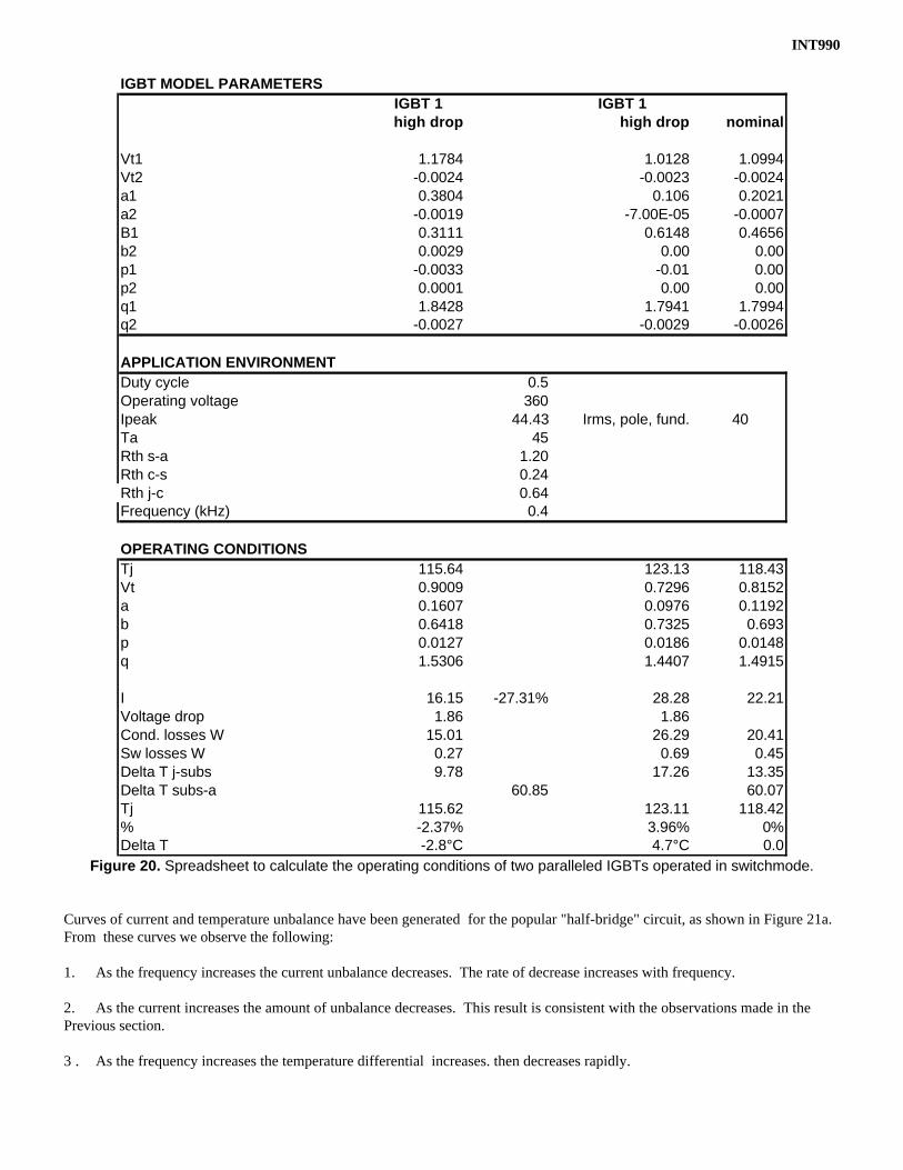
The operating conditions can be calculated with a spreadsheet similar to that shown in Figure 18, except that additional entriesare required for the switching losses (Figure 20).
Tn = 56.6°C∆∆T = +0.5°C
-4.4
Tn = 67.0°C∆∆T = +17.9°C
-19.5
Tn = 93.5°C∆∆T = +34.0°C
-32.8
SEPARATE SINK
Tn = 122.8°C∆∆T = +40.6°C
-33.1
Tn = 122.8°C∆∆T = +8.0°C
-6.0
COMMON SUBSTRATE
Tn = 93.5°C∆∆T = +6.5°C
-7.2
SEPARATE SINK
Tn = 67.0°C∆∆T = +3.8°C
-5.2
0 5 10 15 20 25 30 35CURRENT (AMP)
10
20
30
40
50
CO
ND
UC
TIO
N U
NB
ALA
NC
E (%
)
60
70
80
90
100
Figure 19. Conduction unbalance for two paralleledIGBTs as a function of current for three differentthermal designs.
INT990
Figure 20. Spreadsheet to calculate the operating conditions of two paralleled IGBTs operated in switchmode.
Curves of current and temperature unbalance have been generated for the popular "half-bridge" circuit, as shown in Figure 21a.From these curves we observe the following:
1. As the frequency increases the current unbalance decreases. The rate of decrease increases with frequency.
2. As the current increases the amount of unbalance decreases. This result is consistent with the observations made in thePrevious section.
3 . As the frequency increases the temperature differential increases. then decreases rapidly.
IGBT MODEL PARAMETERS IGBT 1 IGBT 1 high drop high drop nominal
Vt1 1.1784 1.0128 1.0994Vt2 -0.0024 -0.0023 -0.0024a1 0.3804 0.106 0.2021a2 -0.0019 -7.00E-05 -0.0007B1 0.3111 0.6148 0.4656b2 0.0029 0.00 0.00p1 -0.0033 -0.01 0.00p2 0.0001 0.00 0.00q1 1.8428 1.7941 1.7994q2 -0.0027 -0.0029 -0.0026 APPLICATION ENVIRONMENTDuty cycle 0.5 Operating voltage 360 Ipeak 44.43 Irms, pole, fund. 40Ta 45Rth s-a 1.20Rth c-s 0.24Rth j-c 0.64Frequency (kHz) 0.4
OPERATING CONDITIONSTj 115.64 123.13 118.43Vt 0.9009 0.7296 0.8152a 0.1607 0.0976 0.1192b 0.6418 0.7325 0.693p 0.0127 0.0186 0.0148q 1.5306 1.4407 1.4915 I 16.15 -27.31% 28.28 22.21Voltage drop 1.86 1.86 Cond. losses W 15.01 26.29 20.41Sw losses W 0.27 0.69 0.45Delta T j-subs 9.78 17.26 13.35Delta T subs-a 60.85 60.07Tj 115.62 123.11 118.42% -2.37% 3.96% 0%Delta T -2.8°C 4.7°C 0.0

INT990
The key balancing mechanism inthis, as in the steady state mode ofoperation, is the differenttemperature coefficients of thevoltage drop.
As we have seen in the previoussection, an increase in currentcauses an increase in temperaturewhich, in turn, causes a reductionin voltage drop that is larger for theIGBT with a higher voltage drop.Hence, an increase in temperatureresults in a reduction in currentunbalance.
Switching losses increase junctiontemperature of both IGBTs andcontribute to reduce the currentunbalance.
However, the increase intemperature is higher for the IGBTwhich carries the higher current,on account of its higher conductionand switching losses.
This delays the balancingmechanism and causes the increasein temperature differentialnoticeable in Figure 21 between 10and 30 kHz (I = 20ARMS). Thethermal coupling and the differencein temperature coefficientsgradually cause a reduction in thecurrent unbalance.
This, in turn, reduces conductionand switching losses in the IGBTthat was carrying more current,thereby bringing about a morebalanced operating condition at anexponential rate. For the specificIGBTs we have modeled the pointof current balance occurs at atemperature that is somewhathigher than 150°C.
At this point there will still be a temperature differential, on account of different switching losses. It is entirely possible thatIGBTs with different characteristics may reach current balance at a lower temperature, beyond which the unbalance wouldreverse.
Operation at lower duty cycles is not significantly different from what we have just described (Figure 21b), except that thecurrent unbalance for a given output current is lower.
This is due to the third balancing mechanism, whereby the voltage drops converge at higher currents. To generate the sameoutput current with a lower duty cycle a higher peak current is necessary, with intrinsically better current sharing.
I = 20 ARMS
Tn = 78.7°C∆∆T = +4.2°C
-3.1
I = 30 ARMS
Tn = 96.0°C∆∆T = +4.3°C
-3.5
I = 40 ARMS
Tn = 118.4°C∆∆T = +4.7°C
-2.8
Tn = 120.6°C∆∆T = +4.9°C
-2.7
Tn = 124.3°C
∆∆T = +5.0°C -2.6
Tn = 146.4°C∆∆T = +3.0°C
-2.0
Tn = 145.2°C∆∆T = +5.6°C
-2.3
Tn = 131.7°C∆∆T = +4.9°C
-2.4
Tn = 148°C∆∆T = +9.3°C
-2.4
Tn = 131.6°C∆∆T = +12.7°C
-2.2
Tn = 115.4°C∆∆T = +13.5°C
-1.5
Tn = 100.2°C∆∆T = +11.6°C
-1.4
Tn = 86.8°C∆∆T = +7.5°C
-2.29
Tn = 78.7°C∆∆T = +4.2°C
-3.1
Tn = 102°C∆∆T = +5.6°C
-3.2 Tn = 109.2°C∆∆T = +6.9°C
-3.0
Tn = 119.4°C∆∆T = +7.6°C
-2.9
260V
DUTY CYCLE = 50%
0.1 1 10 1000
10
20
30
40
50
60
70
FREQUENCY (kHz)
CU
RR
EN
T U
NB
ALA
NC
E (%
)
Figure 21a. Duty cycle at 50%
I = 10 ARMS
Tn = 55.9°C
∆∆T = +1.1°C -1.4
Tn = 55.6°C
∆∆T = +1.1°C -1.4
Tn = 57.7°C
∆∆T = +2.2°C -1.2
Tn = 61.8°C
∆∆T = +4.7°C -0.5
Tn = 76.5°C
∆∆T = +4.3°C -1.8
Tn = 91.0°C
∆∆T = +8.0°C -1.3
Tn = 70.0°C
∆∆T = +10°C -1.4
Tn = 92.9°C
∆∆T = +19.3°C -3.6
Tn = 114.6°C
∆∆T = +9.9°C -1.8
Tn = 129.3°C
∆∆T = +18.1°C -0.2
Tn = 141.6°C
∆∆T = +6.7°C -2.3
Tn = 142.2°C
∆∆T = +3.8°C -1.8
Tn = 119.8°C
∆∆T = +6.2°C -2.1
Tn = 91.3°C
∆∆T = +4.0°C -2.1
Tn = 87.7°C
∆∆T = +3.3°C -2.1
Tn = 70.0°C
∆∆T = +2.3°C -2.0
Tn = 91.3°C
∆∆T = +4.0°C -2.1 Tn = 102.4°C
∆∆T = +5.5°C -2.0
I = 20 ARMS
I = 30 ARMS
DUTY CYCLE = 20%
360V
IRMS
0.1 1 10 1000
10
20
30
40
50
60
70
FREQUENCY (kHz)
CU
RR
EN
T U
NB
ALA
NC
E (%
)
Figure 21b. Current and temperature unbalance as a function of frequency oftwo IGBTs operated in parallel.

INT990
C. Conclusions
Although the analysis presented in the previous sections is limited to one specific type of IGBTs in a specific operating mode,the results have been found to be equally applicable to the other families of IGBTs available from International Rectifier at thetime of writing. They can he summarized as follows:
1. Paralleled IGBTs will operate with a current unbalance that, in a practical application, can be as high as 50 to 70% at lowcurrents. Temperature unbalance, on the other hand, is generally less than 10°C, provided they are on the same heatsink.
2. Three balancing mechanisms tend to reduce the current unbalance:
∗ thermal feedback;∗ different temperature coefficients of the voltage drop;∗ converging voltage drop characteristics at higher currents.
3. The tighter the thermal coupling, the lower the unbalance. Operation of paralleled IGBTs on separate heatsinks should beavoided.
4. An increase in junction temperature reduces the unbalance, on account of the different temperature coefficients of the
voltage drop. An increase in frequency has the same effect, for the same reason. 5. An increase in current reduces the unbalance, due to converging dynamic resistances. It would also cause an increase in
temperature and, consequently, a further reduction in unbalance. 6. For a given output current, a decrease in duty cycle causes an increase in peak current, hence a reduction in unbalance.
X. SCREENING OF IGBTS FOR PARALLELING
In this section we will cover the following:
∗ Discuss one method of device selection to achieve better sharing, and compare performance achieved for IR’s 600V FastIGBTs.
∗ Compare performance achieved for IR’s 600V UltraFastTM IGBTs.∗ Discuss multiple (> 2) parallel IGBT designs.
X.A. Screening method for IR’ 600V Fast IGBT
Device selection is an effective method to reduce derating that is intrinsicallyassociated with paralleling and ensure that IGBTs are operated within datasheet limits. As a selection criteria, the voltage across each IGBT wasmeasured at a certain current level. The configuration of this measurement iswhat we call “diode mode” (Figure 22) which means the gate is tied to thecollector, and voltage is applied across that combined terminal and the emitter.
The voltage is increased until the desired current is conducted through theIGBT. This measurement must be done in pulse mode to avoid device self-heating. The voltage required for this amount of current is recorded. Thismeasurement not only takes into account variations in VCE(on), but alsothreshold, as well as gfs. This “diode mode” voltage results in a convenientway to select IGBTs that will be paralleled.
Matching only VCE(on) would be more appropriate for IGBTs not operated in Switchmode. In the following two sections,simulations have been run on different pairs of IGBTs to compare temperature unbalance and current unbalance versus devicevariation measured using the “diode mode” voltage of the IGBT.
IC
Figure 22. Connection for Measuring"Diode Mode" Voltage, V diode

INT990
Using this device selection strategy, we set outto devise a method of determining how wellvarious pairs of IGBTs parallel in a typical half-bridge configuration. To this end, an empiricalmodel was used for our IGBTs that modelsconduction and switching loss described inSections III.B and IV.B.
Five devices from each lot, using three lots, wereexamined and ranked in order of conductionvoltage. Using this information, it is possible toobtain the operating point of IGBTs in paralleloperation.
To compare performance of various sets ofIGBTs, graphs of percent current unbalanceversus total current were developed. Thesegraphs depict how much D.C. current unbalancecan be expected for a given total current, for aparticular pair of IGBTs.
Two cases are plotted - devices mounted on separateheat sinks and devices mounted on a common heatsink. Also generated were graphs of junctiontemperature of the higher of the two junctionsversus total current. In these graphs, three curvesare plotted: 1) perfectly matched devices with nounbalance, 2) devices unmatched by a value of∆Vdiode, mounted on the same heat sink, and 3)devices unmatched by a value of ∆Vdiode, mountedon separate heat sinks.
Figure 23 depicts the percent current unbalance atdifferent current levels for the two IRGPC50Fs atboth ends of the spectrum: one has the lowestVCE(on), while the other has the highest VCE(on) ofall the devices tested. The ∆Vdiode for this pair ofIGBTs was 0.69V. The operating conditions were:two devices mounted on either a common heatsink with an RθSA of 2°C/W, or separate heat sinkswith RθSAs of 4°C/W, with an ambienttemperature of 45°C.
As Figure 23 shows, at low currents, one IGBTcarries all the current. As the current increases,the unbalance improves due to the three balancingmechanisms we mentioned above for the lowercurve (same heat sink, therefore tight thermalcoupling) and just the two related to current forthe upper curve (separate heat sink).
Figure 24 depicts the higher junction temperature of the two IGBTs in parallel for three different cases: perfectly matcheddevices, the above two devices mounted on the same heat sink and the above two devices mounted on different heat sinks. Thisfigure provides the strongest argument for placing separate devices on the same heat sink: while conducting 20 A, the two worstcase IGBTs’ junction temperatures are within 2.5°C of the ideal case of perfectly matched IGBTs. However, the junctiontemperature of one of these same two devices mounted on separate heat sinks operates at an increased junction temperature of16°C. Also note that the maximum allowable current is reduced from 35 A to 31 A. All solely due to the devices’ being mountedon separate heat sinks.
Ambient Temp = 45°CSeparate Heat Sinks
w/ RthSA = 4°C/W each
Common Heat Sinkw/ RthSA = 2°C/W
0 5 10 15 20 25 30 350%
10%
20%30%40%
50%
60%
70%80%
90%100%
Current in A
% C
urre
nt U
nbal
ance
Figure 23. Percent Current Unbalance versus Total Current,IRGPC50F with ∆Vdiode = 0.69V
Separate Heat Sinkw/ RthSA = 4°C/W each
Common Heat Sinkw/ RthSA = 2°C/W each
Identical DevicesCommon Heat Sinkw/ RthSA = 2°C/W
Ambient Temp = 45°C
5 10 15 20 25 30 3550
75
100
125
150
Current in A
Tj i
n °C
Figure 24. Junction Temperature versus Total Current, IRGPC50Fwith DVdiode = 0.69V
Ambient Temp = 45°C
Separate Heat Sinksw/RthSA = 4°C/W each
Common Heat Sinksw/RthSA = 2°C/W
0 5 10 15 20 25 30 350%
10%
20%
30%
40%50%
60%70%
80%
90%
100%
Current in A
% C
urre
nt U
nbal
ance
Figure 25. Percent Current Unbalance versus Total Current,IRGPC50F with ∆Vdiode = 0.33V

INT990
The two devices in Figures 23 and 24 exhibitedthe largest range in Vdiode of all 15 devices tested.The difference in “Vdiode” voltages was 0.69 Vmeasured at 20 A.
For two devices that had a difference of 0.33 V at20A, the graphs are shown in Figures 25 and 26.These devices, mounted on separate heat sinks,are limited to a maximum current of 33 A, whiledevices on a common heat sink can operate to 35A.
While conducting 20 A, the two IGBTs’ junctiontemperatures are within 1.5°C of the ideal case ofperfectly matched IGBTs when mounted on acommon heat sink. The same two devicesmounted on separate heat sinks operate at anincreased junction temperature of 8.3°C.
Figures 27 and 28 depict the correlation of currentunbalance and junction temperature to the“Vdiode” screening parameter.
From these two figures, it is possible to predict theoperation of a parallel pair of IGBTs given thedifference in their “diode mode” voltages.
Figure 29 depicts the reduction in output currentin a half-bridge circuit due to junctiontemperature limitations between unmatchedIGBTs.
The circuit is operated under the same conditions as the previous ones, but instead of the current being fixed, the junctiontemperature is fixed at 125°C. Neither IGBT is allowed to exceed 125°C. The graph plots the maximum output current versusswitching frequency. Notice that little or no derating is necessary under common applications or conditions.
The curves in Figure 29 were calculated assuming the two devices were mounted on a common heat sink. The case of separateheat sinks was not addressed due to concerns previously mentioned.The output current would be significantly reduced if the devices were on different heat sinks.
Separate Heat Sinksw/RthSA = 4°C/W each
Common Heat Sinksw/RthSA = 2°C/W each
Identical DevicesCommon Heat Sinks
w/RthSA = 2°C/W
Ambient Temp = 45°C
5 10 15 20 25 30 35
Current in A
50
75
100
125
150
Tj i
n °C
Figure 26. Junction Temperature versus Total Current, IRGPC50F with∆Vdiode = 0.33V
Separate Heat Sinksw/RthSA = 4°C/W each
Common Heat Sinkw/RthSA = 2°C/W
0 0.1 0.2 0.3 0.4 0.5 0.6 0.70%
5%
10%
15%
20%
25%
30%
35%
"Diode Mode" Voltage
% C
urre
nt U
nbal
ance
Figure 27. Percent Current Unbalance versus ∆Vdiode, IRGPC50F
Figure 28. Junction Temperature versus ∆Vdiode, IRGPC50F
Separate Heat Sinksw/RthSA = 4°C/W each
Ambient Temp = 45°CTotal Current = 20A
Commom Heat Sinkw/RthSA = 2°C/W
0 0.1 0.2 0.3 0.4 0.5 0.6 0.794
96
98
100
102
104
106
108
110
112
"Diode Mode" Voltage
Tj i
n °
C
Curves are for:Identical Devices (top curve)Devices from Figures 4 & 5Devices from Figures 2 & 3
Common Heat Sinkw/RthSA = 2°C/W
Half-Bridge 50% Duty CycleAmbient Temp = 45°C
0.1 1 10
15
20
25
30
35
40
45
RM
S C
urr
en
t in
A
Freq in kHz
Figure 29. Current versus Frequency Graph for Three Pairs ofIRGPC50Fs with ∆Vdiode = 0.00, 0.33, & 0.69V

INT990
X.B. Device Selection for IR’s 600V Ultra Fast IGBT
The method presented in the previous sectionwas found to be inappropriate when the amountof lifetime killing has a significant impact onthe behavior of the device. For these devices, asimple VCE(on) matching scheme has beenimplemented. The following figures describe theperformance achieved using various pairs ofparalleled UltraFast IGBTs.
Figure 30 depicts the percent current unbalanceat different current levels for the twoIRGPC50Us at both ends of the spectrum:lowest and highest V CE(on)s of the entirepopulation of 15 devices from three lots. The∆VCE(on) for these was 0.55 volts measured at 30amps. The operating conditions were: twodevices mounted on a common heat sink with anRθSA of 2°C/W with an ambient temperature of45°C.
While the current sharing displayed in Figure 30may appear to be unacceptable, as discussed inthe previous section, the more important factoris the junction temperature, which is shown inFigure 31. The upper curve in Figure 10 is forthe devices in Figure 30, while the lower curveis for two identical (i.e., ∆VCE(on) is zero). Forany current the penalty resulting frommismatched devices is only a few degreesCelsius.
To compare closer matched devices, the abovetwo figures were repeated using two deviceswith a ∆VCE(on) = 0.36V measured at 30 amps.Figure 32 depicts the percent current unbalanceat different current levels for two mismatchedIRGPC50Us. The operating conditions are thesame as the previous two figures.
Figure 33 depicts the junction temperatureversus current. The upper curve in Figure 33 isfor the devices in Figure 32, while the lowercurve is for two identical (i.e., ∆VCE(on) is zero).
Figure 34 depicts the higher of the two junctiontemperatures for the parallel combination ofseveral different pairs of IRGPC50Us withincreasing ∆VCE(on)s. This graph shows thatscreening is not very effective and that it iscritically important that paralleled devices bemounted on a common heat sink.
The final graph, Figure 14, depicts the RMS current versus switching frequency for a parallel pair of IRGPC50Us operated in atypical half-bridge configuration with 50% fixed duty cycle. The devices are mounted on a common heat sink with a thermalresistance of 2°C/W with an ambient temperature of 45°C. Neither IGBT is allowed to exceed a junction temperature of 125°C.
0 5 10 15 20 25 300%
10%20%
30%
40%
50%
60%70%
80%
90%100%
Current in A
% C
urre
nt U
nbal
ance
Common Heat Sinkw/RthSA = 2°C/W
Ambient Temp = 45°C
Figure 30. Percent Current Unbalance versus Total Current,IRGPC50U with ∆VCE(on) = 0.55V
MismatchedDevices
Identical Devices
Common Heat Sinkw/RthSA = 2°C
Ambient Temp = 45°C
0 10 15 2520 3050
75
100
125
150
Current in A
Tj i
n °C
Figure 31. Junction Temperature versus Total Current, IRGPC50Uwith ∆VCE(on) = 0.55V
Common Heat Sinkw/RthSA = 2°C/W
Ambient Temp = 45°C
0 5 10 15 20 25 300%
10%20%
30%
40%
50%
60%70%
80%
90%100%
Current in A
% C
urre
nt U
nbal
ance
Figure 32. Percent Current Unbalance versus Total Current,IRGPC50U with ∆VCE(on) = 0.36V
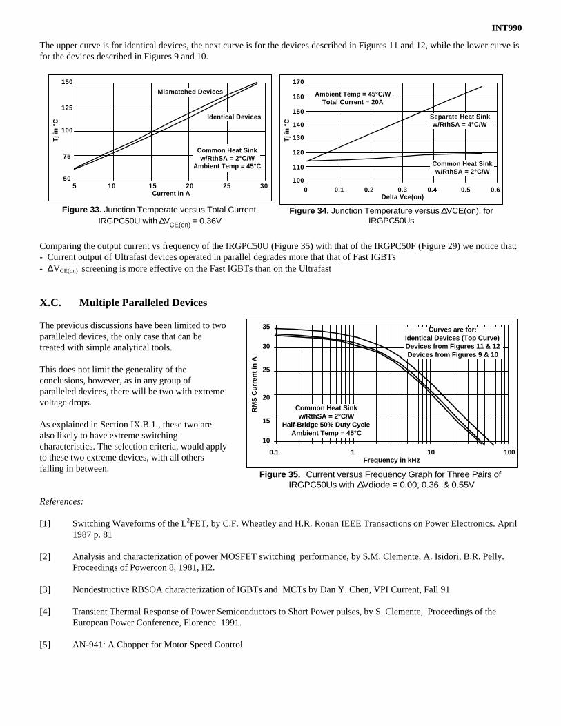
INT990
The upper curve is for identical devices, the next curve is for the devices described in Figures 11 and 12, while the lower curve isfor the devices described in Figures 9 and 10.
Comparing the output current vs frequency of the IRGPC50U (Figure 35) with that of the IRGPC50F (Figure 29) we notice that:- Current output of Ultrafast devices operated in parallel degrades more that that of Fast IGBTs- ∆VCE(on) screening is more effective on the Fast IGBTs than on the Ultrafast
X.C. Multiple Paralleled Devices
The previous discussions have been limited to twoparalleled devices, the only case that can betreated with simple analytical tools.
This does not limit the generality of theconclusions, however, as in any group ofparalleled devices, there will be two with extremevoltage drops.
As explained in Section IX.B.1., these two arealso likely to have extreme switchingcharacteristics. The selection criteria, would applyto these two extreme devices, with all othersfalling in between.
References:
[1] Switching Waveforms of the L2FET, by C.F. Wheatley and H.R. Ronan IEEE Transactions on Power Electronics. April1987 p. 81
[2] Analysis and characterization of power MOSFET switching performance, by S.M. Clemente, A. Isidori, B.R. Pelly.Proceedings of Powercon 8, 1981, H2.
[3] Nondestructive RBSOA characterization of IGBTs and MCTs by Dan Y. Chen, VPI Current, Fall 91
[4] Transient Thermal Response of Power Semiconductors to Short Power pulses, by S. Clemente, Proceedings of theEuropean Power Conference, Florence 1991.
[5] AN-941: A Chopper for Motor Speed Control
Separate Heat Sinkw/RthSA = 4°C/W
Common Heat Sinkw/RthSA = 2°C/W
Ambient Temp = 45°C/WTotal Current = 20A
0 0.1 0.2 0.3 0.4 0.5 0.6100
110
120
130
140
150
160
170
Delta Vce(on)
Tj i
n °C
Figure 34. Junction Temperature versus ∆VCE(on), forIRGPC50Us
Mismatched Devices
Identical Devices
Common Heat Sinkw/RthSA = 2°C/W
Ambient Temp = 45°C
5 10 15 20 25 3050
75
100
125
150
Tj i
n °C
Current in A
Figure 33. Junction Temperate versus Total Current,IRGPC50U with ∆VCE(on) = 0.36V
Curves are for:Identical Devices (Top Curve)Devices from Figures 11 & 12Devices from Figures 9 & 10
Common Heat Sinkw/RthSA = 2°C/W
Half-Bridge 50% Duty CycleAmbient Temp = 45°C
0.1 1 10 100
10
15
20
30
25
35
Frequency in kHz
RM
S C
urre
nt in
A
Figure 35. Current versus Frequency Graph for Three Pairs ofIRGPC50Us with ∆Vdiode = 0.00, 0.36, & 0.55V

INT990
APPENDIX 1: DESCRIPTION OF THE CURVE FITTING METHODS USEDTO DERIVE THE MODEL PARAMETERS.
The conduction model presented in Section III fulfills the basic requirements of accuracy and simplicity. As it shown in Table II,it lends itself to easy integration, thus providing a closed form expression for the conduction losses of common waveforms.
The parameters of the model are extracted from the averages and standard deviations taken at a given temperature on apopulation of IGBTs from three different lots, as shown in Table A.1.
To calculate a and b the model is manipulated as follows:
Vce = Vt + a Ib
Vce - Vt = a Ib
ln (Vce - Vt) = ln a + b ln I
This last expression is a straight line fit to the natural logarithmsof I and Vce - Vt.
Using the least square method, the values of ln a and b can beobtained by the following formulas:
( ) ( )[ ] ( )[ ] ( )[ ]( ) ( )[ ]
bn x V V I x V V
n I I
i CE t i i CE t i
i i
=− − −
−
∑ ∑∑
∑∑
ln ln ln ln
ln ln2 2
( ) ( )ln
ln ln=
−−
∑ ∑V V
nb
I
nCE t i i
a e a= ln
The value of Vt has been defined as the voltage drop at a currentdensity of approximately 0.035 a/mm2, which, for the IGBT ofTable A.1, corresponds to 0.6A. With this in mind, Table A.2shows the calculations and the error.
The values entered in Table A.2 correspond to the averages of Table A.1. If the average-plus-three-sigma values had beenentered, the model parameters would correspond to the data entered.
This process can be repeated for different temperatures and a set of model parameters would be obtained. Each element of the setprovides an accurate model of the specific IGBT at a specific temperature.
VCE(ON) DEVICE BC40FLOT #'S: FS4
FQ8FB3
TEMP 100°C
lC (A) > 0.6 8 16 32 50
1 0.694 1.127 1.418 1.925 2.462 0.678 1.114 1.413 1.94 2.53 0.677 1.097 1.382 1.885 2.44 0.685 1.112 1.399 1.899 2.425 0.711 1.178 1.485 2.01 2.576 0.743 1.263 1.604 2.19 2.837 0.732 1.223 1.541 2.09 2.678 0.723 1.206 1.524 2.08 2.669 0.746 1.264 1.602 2.19 2.81
10 0.731 1.223 1.543 2.09 2.6711 0.694 1.157 1.47 2.01 2.612 0.714 1.193 1.513 2.06 2.6513 0.714 1.189 1.506 2.05 2.6514 0.7 1.147 1.512 1.98 2.55
1 5 0.706 1.1 51 1.47 1.99 2.56
MINIMUM 0.677 1.097 1.382 1.885 2.400MAXIMUM 0.746 1.264 1.604 2.190 2.830AVERAGE 0.71 1.176 1.492 2.026 2.600
STD 0.021 0.051 0.066 0.091 0.122
AVG + 6STD 0.838 1.484 1.888 2.572 3.331AVG-6STD 0.581 0.868 1.097 1.480 1.869
Table A.1. Conduction Characteristics of a Population of IGBTs from three different slots
A V V cal V-Vcal Error V-vt In(V-Vt) In(l) (XiYi)0.60 0.71 0.77 -0.0645 -9.08%8.00 1.18 1.17 0.0026 0.22% 0.4660 -0.7636 2.0794 -1.5878
16.00 1.49 1.50 -0.0035 -0.23% 0.7820 -0.2459 2.7726 -0.681832.00 2.03 2.04 0.0155 -0.76% 1.3160 0.2746 3.4657 0.951750.00 2.60 2.58 0.0198 0.76% 1.8900 0.6366 3.9120 2.4903
n = 4 -0.0983 12.2298 1.1724Sum Yi Sum Xi Sum XiYiVarian 0.4837
b = 0.7614 ln a = -2.3524
a = 0.0951
Table A.2. Calculation of the Voltage Drop Parameters

INT990
Unfortunately, in most design problems the junction temperature is the unknown (see Figure 11, 18 and 20) and fixedtemperature parameters, like those shown in Table A.2 are not useful.
Assuming that these parameters have a simple temperature dependence, a linear regression has been done, as shown in TableA.3.
This provides the expression of the voltage drop as a function of current and temperature with which we have analyzed theoperating conditions of Figure 11, 18 and 20. As shown in Table A.3 the accuracy of the parameter obtained with the linearregression is within few Percent.
The switching model parameters are obtained in a very similar way, using the same type of expression, except for the threshold.The accuracy of the linear regression to calculate the temperature coefficients is acceptable for some IGBTs, particularly theStandard and the Fast, while an exponential regression is more accurate for the Ultrafast. For the sake of simplicity, only thelinear regression is listed in Tables I and III.
APPENDIX 2: Equations to identify the operating point of paralleled IGBTs.
In the system described in sections IX.B.1 and B.2 the parameters listed in the two top boxes of Figure 20 are known, while thoselisted in the third box have to be calculated. The two fundamental constraints that determine the current distribution between theIGBTs are the following:
∗ voltage drop across the two IGBTs is the same;∗ the sum of the currents is the same and equal to the load current.
Imposing these two constraints to the voltage drop model we obtain the following:
V VCE CE− −=1 2( ) ( )V a I V a ITb
Tb
− − −−
− − −−+ = +1 1 1
212 2 2
2
( )II
b
V V
a
a
q
IL T T Lb
2
1
22
1 2
2
1
2
1+
= − +
−
− −
−
−
−
−∆ exp ln
where the index after the dash identifies the IGBT, while the index before the dash identifies the model parameter, e.g. VTI 2identifies the first threshold parameter (see Figure 18) of the second IGBT.
Since the key unknowns are ∆I, T l and T 2, we need two additional expressions, which can be obtained from the thermalequations:
Temp a a (calc) Error b b (calc) Error Vt Vt Calc Error25 0.0778 0.7391 0.8550 0.0814 0.0832 -2.23% 0.7523 0.7469 0.72% 0.80 0.80 -0.40%75 0.0899 0.0886 1.27% 0.7496 0.754- -0.69% 0.76 0.76 0.28%
100 0.0951 0.0941 1.13% 0.7614 0.7626 -0.16% 0.71 0.71 0.34%125 0.1009 0.0995 1.40% 0.7668 0.7704 -0.48% 0.66 0.66 0.26%150 0.103 0.1049 -1.86% 0.7829 0.7733 0.59% 0.61 0.61 -0.49%500 0.4703 3.8129 3.5380 6.83E-02
(XiYi) = 48.3873 (XiYi) = 383.2507 (XiYi) = 341.7250Sxi^2 = 56250
a = a1 + a2*T a1 = 0.0724 a2 = 2.17E-04b = b1 + B2*T b1 = 0.7313 b2 = 3.13E-04Vt = Vt1 + Vt2*T Vt1 = 0.9008 Vt2 = -1.9E-03
Table A.3. Linear Regression for Temperature Coefficient of Voltage Drop Parameters

INT990
( )( ) ( )
T T I V a I
I V a I I V a I
A L Tb
SA
Tb
Tb
JS
− − − −−
− − − − − − −+
= + +
+ +
− +
1 2 2 22
2 22
2 2 2 21
θ
θ
The first of these expression is calculated in the cell shown on the right of the Operating Conditions box with the "solve for"function, with the parameters shown in the box. Successive calculations of current and temperature yield the final result. Forthese calculations the following simplification was made in the first expression:
( )( )V V V V T TT T T T− − − −− ≅ − −1 2 2 1 2 2 1 2
of minimal impact on overall accuracy.
WORLD HEADQUARTERS: 233 Kansas St., El Segundo California 90245, Tel: (310) 322 3331EUROPEAN HEADQUARTERS: Hurst Green, Oxted, Surrey RH8 9BB, UK Tel: ++ 44 1883 732020
IR CANADA: 7321 Victoria Park Ave., Suite 201, Markham, Ontario L3R 2Z8, Tel: (905) 475 1897IR GERMANY: Saalburgstrasse 157, 61350 Bad Homburg Tel: ++ 49 6172 96590
IR ITALY: Via Liguria 49, 10071 Borgaro, Torino Tel: ++39 11 451 0111IR FAR EAST: K&H Bldg., 2F, 3-30-4 Nishi-Ikeburo 3-Chrome, Toshima-Ki, Tokyo Japan 171 Tel: 81 3 3983 0086
IR SOUTHEAST ASIA: 315 Outram Road, #10-02 Tan Boon Liat Building, Singapore 0316 Tel: 65 221 8371Data and specification subject to change without notice.
( )
( )T T I V a I
I V a I
A L Tb
SA
Tb
JS
− − − −−
− − − −− +
= + −
+ +
2 2 2 22
2 2 2 22 1
θ
θ