app. notes of ccir 3band tuner for tua6030 components application note of isdb-t tuner with tua...
TRANSCRIPT
Wireless Components
Application Note of ISDB-T Tuner with TUA 6034T
Version 1
Applications of IC TUA6034T : Specially Suitable for Digital Broadcasting Standards
like DVB-T, DVB-C, ISDB-T, ATSC, etc.
SMS M AE DS 2003-07-01

July 01, 2003
Page 1 Wireless products Application Engineering SMS M AE DS
Overview of the ISDB-T Tuner
Single Conversion Tuner for ISDB-T application
With Infineon Components of
TUA 6034T Single Chip Mixer-Oscillator-PLL IC
BF 2030W self biasing MOSFET
BG 3130 Dual MOSFET
BB555, BB565, and BB659C Varactor Diodes
This very small sized single conversion tuner designed for ISDB-T front-end in the frequency range from 93 to 767 MHz can be used with minimum modifications for all digital broadcasting receptions. The tuner was developed as a real 3 band tuner concept, designed without switching diodes based on the Infineon 3 band tuner IC TUA6034T which has 3 mixer, 3 oscillators, separated SAW driver input, PLL, and balanced crystal oscillator for optimum digital front-end performance. The IC is particularly suitable for COFDM applications like DVB-T and ISDB-T that requires stringent close-in phase noise. The IC provides a balanced SAW filter driver output that is designed to drive a SAW filter directly. The tuner is optimized for IF bandwidth = 6 MHz and IF center frequency = 57 MHz. The frequency ranges of the tuner are as follows :
VHF I : 93- 167 MHz VHF II : 173- 467 MHz UHF : 473- 767 MHz
All the passive and active components except air coils, 1 choke coil, are SMD components. The PCB is single-clad and the dimensions are 49.5 x 38.5 mm. The pin layout and the outline dimensions are designed according to the world standard tuner description, which is the current standard size of analog tuners in the market. Semiconductors:
T U A 6 0 3 4
B F 2 03 0W
B B 56 5 B B 65 9C
1 X
3 X 8 X
TU A 603 4T 1 X
B B 55 5 4 X
1 X B G 3 13 0

July 01, 2003
Page 2 Wireless products Application Engineering SMS M AE DS
Contents
1. Tuner Design......................................................................................................... 3 1.1 Circuit concept ................................................................................................. 3 1.2 UHF RF Block .................................................................................................. 4 1.3 VHFH RF Block................................................................................................ 4 1.4 VHFL RF Block ................................................................................................ 4 1.5 Oscillator Resonator, PLL Loop Filter & Phase Noise..................................... 5 1.6 IF Block ............................................................................................................ 7
2. PCB ........................................................................................................................ 7
3. TUA 6034T One Chip Multimedia Tuner IC ........................................................ 8 3.1 Highlights ......................................................................................................... 8 3.2 Block diagram .................................................................................................. 9
4. Alignment ............................................................................................................ 10 4.1 Alignment set-up ............................................................................................ 10 4.2 Alignment Procedures.................................................................................... 11
5. Measurement Results ........................................................................................ 12 5.1 Electrical Characteristics of the Tuner ........................................................... 12 5.2 Measurement graphs ..................................................................................... 14
6. PLL Programming .............................................................................................. 23
7. Component Lists ................................................................................................ 24
8. Circuit and Layout .............................................................................................. 27 8.1 Circuit Diagram .............................................................................................. 27 8.2 Layouts........................................................................................................... 28 8.3 Pin Layout & Outline Dimensions ................................................................. 28
9. Automatic Tuner Test Set-up ............................................................................ 29
10. Ordering & Contact Information ....................................................................... 30
July 01, 2003
Page 3 Wireless products Application Engineering SMS M AE DS
1. Tuner Design 1.1. Circuit Concept The RF input signal is splitted by a simple high pass filter combined with IF & CB (Citizen Band) traps. Instead of band switching with PIN diodes a very simple triplexer circuit is used. With a high inductive coupling the antenna impedance is transformed to the tuned input circuits. The pre-selected signal is then amplified by the high gain self biased MOSFET BF2030W (UHF). One BG3130 double-MOSFET is used for both VHF bands. In the following tuned bandpass filter stage the channel is selected and unwanted signals like adjacent channels and image frequency are rejected. Tracking traps of prestages and capacitive image frequency compensations of band filters reject especially image frequencies. The conversion to IF is done in the one chip tuner-PLL IC TUA 6034T. The TUA6034T is a real 3 band tuner IC which has all the active parts for the 3 mixers, 3 oscillators, an IF driver stage, the complete PLL functions including 4 PNP ports & 1 NPN port (ADC input) for the band switching, and a wideband AGC detector for internal tuner AGC. Combined with the optimized loop filter, 4 programmable charge pump currents, the balanced crystal oscillator, and the voltage controlled oscillators which have superb characteristics thanks to Infineon's B6HF technology, the tuner can achieve distinguished phase noise performance suitable for all digital applications. The balanced IF output signal of the TUA6034T is designed to drive directly a SAW filter in the following IF stage. The tuner consumes less than 90 mA currents or 0.45 Watt power. This can be a big advantage for portable or handheld appliances.
Fig. 1. Example of a circuit concept diagram of an ISDB-T tuner
July 01, 2003
Page 4 Wireless products Application Engineering SMS M AE DS
1.2. UHF RF Block
With the wide range ultra linear varactor diode BB555 it has become possible to design an UHF band without coupling diodes and without compensating coils for extending the frequency ratio in the tuned filters. To get a good tracking without a coupling diode between the input filter and the MOSFET the point of coupling is set between the tuning diode and the series capacitor, and not at the high end of the resonant circuit. The bandpass stage is an inductive low end coupling filter, which concurrently provides the transformation from unbalanced to balanced. Also thanks to the matched image filters on both prestage and band pass filter stage, better than 80dB image rejection can be achieved over the whole UHF band. By means of simple gate 1 switching through PNP ports, pre-amplifiers are selected. 1.3. VHFH RF Block For VHFH band, high quality ratio-extended varactor diode, BB659C is used. To compensate gain, one additional coupling diode, BB565 is placed in the prestage of VHFH. The RF bandpass filter is unbalanced on the primary side, and balanced on the secondary side just like UHF band pass filter. The coupling between filters is realized via a printed inductor. The mixer input circuit is optimized to protect the mixer from overloading. Image rejection filters work as those of UHF block. 1.4. VHFL RF Block For the wide VHFL frequency range a tuning diode with an extended capacitance ratio is required. BB659C is a tuning diode, which was developed to cover the wide frequency range of Hyperband tuner and at the same time shows a low series resistance. 2 x BB565 are used for coupling to achieve improved RF characteristics. The RF band pass filter is unbalanced, and is also coupled asymmetrically to the high ohmic VHFL mixer, which has no negative effects due to the relatively low frequencies involved. After the RF Block circuit design it is preferable to do block simulations to confirm its frequency dependent characteristics.
July 01, 2003
Page 5 Wireless products Application Engineering SMS M AE DS
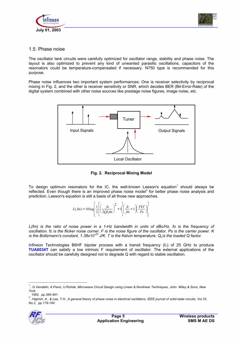
1.5. Phase noise The oscillator tank circuits were carefully optimized for oscillator range, stability and phase noise. The layout is also optimized to prevent any kind of unwanted parasitic oscillations, capacitors of the resonators could be temperature-compensated if necessary. N750 type is recommended for this purpose. Phase noise influences two important system performances: One is receiver selectivity by reciprocal mixing in Fig. 2, and the other is receiver sensitivity or SNR, which decides BER (Bit-Error-Rate) of the digital system combined with other noise sources like prestage noise figures, image noise, etc.
Fig. 2. Reciprocal Mixing Model To design optimum resonators for the IC, the well-known Leeson's equation1 should always be reflected. Even though there is an improved phase noise model2 for better phase noise analysis and prediction, Leeson's equation is still a basis of all those new approaches.
L(fm) is the ratio of noise power in a 1-Hz bandwidth in units of dBc/Hz. fo is the frequency of oscillation. fc is the flicker noise corner. F is the noise figure of the oscillator. Ps is the carrier power. K is the Boltzmann's constant, 1.38x10⁻²³ J/K. T is the Kelvin temperature. QLis the loaded Q factor. Infineon Technologies B6HF bipolar process with a transit frequency (fT) of 25 GHz to produce TUA6034T can satisfy a low intrinsic F requirement of oscillator. The external applications of the oscillator should be carefully designed not to degrade Q with regard to stable oscillation.
1. G.Vendelin, A.Pavio, U.Rohde, Microwave Circuit Design using Linear & Nonlinear Techniques, John Wiley & Sons, New York, 1992, pp.385-491. 2. Hajimiri, A., & Lee, T.H., A genaral theory of phase noise in electrical oscillators, IEEE journal of solid-state circuits, Vol.33, No.2, pp.179-194.
Tuner
Input Signals Output Signals
Local Oscillator
+
+
=PsFkT
fmfc
QLfmfofmL 11
2
221log10)(
July 01, 2003
Page 6 Wireless products Application Engineering SMS M AE DS
The critical role of loop filter is to remove the reference spurs produced by the phase detection process, which is fundamentally a sampled system in digital implementations. Since the control voltage directly modulates the frequency of the VCO, any AC components of tuning voltage results in a frequency modulation of the oscillator. If these components are periodic, they produce stationary side-bands like reference spurs. Because of the wide tuning range of the tuner, the tuning sensitivity of the tuner can go up to 35 MHz/V, so even a few millivolts of noise on the tuning lines will generate noticeable spectral interference. The oscillator's output now has the benefits of phase locking such as improved stability and phase noise and this is another crucial function of PLL. By determining a proper loop bandwidth, optimum phase noise characteristics of the reference oscillator and the local oscillator can be utilized. For a given loop bandwidth, a higher order filter provides more attenuation of out-of-band spectral components. However, the higher the order, the more poles there are, and it means it gets harder to make the loop stable. The loop bandwidth and loop filter components should be carefully selected to achieve optimal phase noise and to reject reference spurs. 4 extended modes of charge pump currents also must be appropriately chosen and used for best phase noise performance of different frequency ranges. For this tuner design ISDB-T recommended fref = 142.857 kHz is used for all loop filter calculations and measurements. A 3rd order passive loop filer is chosen for the tuner design. The following are simplified procedures to decide the loop filter components. 1. Define the basic synthesizer requirements ; oscillator frequency ranges, fref, maximum frequency step, fBW
(Loop Bandwidth, Hz) with deep consideration of in-out band phase noise. 2. Identify Kvco (VCO sensitivity, Hz/V) and Icp (charge pump current, A). 3. Calculate Fstep = fvco_max - fvco_min, to optimize for fvco_max 4. Calculate N = fvco_max / fref, to optimize for fvco_max. 5. Calculate natural frequency, Fn ; ζ = damping factor
)
41(2
2
ζζπ
×+×
×= BWfFn Hz (2)
6. Calculate C68 ; 2)2(68
nFN
vcoKcpIC××
×=
π Farad (3)
7. Calculate R39, and its phase noise contribution. This completes the main part of the loop filter.
68
239CvcoKcpI
NR××
××= ζ Ohm (4)
××=Φ fm
RTkvcoKfmL
392log20)( dBc/Hz (5)3
8. Calculate C65, which is used to damp transients from the charge pump and should be at least 20 times smaller than C69, i.e.,
206869 CC ≤
3. G.Vendelin, A.Pavio, U.Rohde, Microwave Circuit Design using Linear & Nonlinear Techniques, John Wiley & Sons, New York, 1992, pp.436.
(1)
July 01, 2003
Page 7 Wireless products Application Engineering SMS M AE DS
9. Calculate R40 & C24 within these limits and the phase noise contribution of R40 by Eq. (5).
,40242,39681 RCRC ×=×= ττ 1.01201.0 <<
ττ
A bigger time constant results in somewhat better filtering action, but tends to be associated with lower stability. 10. In order to have the confidence in the stability of the loop, an open loop analysis is performed to estimate the gain and phase margin. By closed loop analysis we can obtain the frequency response & transient response of the loop. We use a mathmatic tool to analyse these parameters though a spreadsheet program is enogh for the above calculations. Typically the crystal oscillator used for the reference has very good phase noise that then levels off near 10 kHz offset at around –150 dBc/Hz. The free running oscillator to be phase locked typically has much higher close in noise but continues down to around –120 dBc/Hz beyond 1 MHz. At some offset the reference noise multiplied up to the output frequency becomes higher than the oscillator's free running noise. This is the point where normally the loop bandwidth is set. Inside the loop the oscillator noise is improved by the reference, yet outside the loop is not degraded by the reference. Because of the wide tuning range of the tuner oscillator the loop bandwidth should be very carefully chosen with deep consideration of these noise contribution mechanism. The phase noise level within the loop bandwidth can be approximated by (6) reffNfloornoisephasenormalizedHznoisephaseinClose log10log20)____1(___ ++= There are other sources of phase noise that need to be considered when designing the tuner. One of the most common sources of noise is the power supply to the IC. This can be caused in many ways, but most commonly are due to supply ripple and electric or magnetic coupling to +5 V line. Correct PCB layout and good AC blocking are critical to ensure good noise performance. The highest level signal line in the tuner is the IF output line, and all those sensitive blocks like oscillator, loop filter and long DC lines should be well-protected from coupling by IF lines. 1.6. IF Block The TUA6034T has separated mixer outputs and SAW driver inputs to realize an IF filter of band pass filter structure that helps much better adjacent channel rejection. Especially in simulcasting signal environment as in Fig.5, it is a big advantage combined with internal AGC of TUA6034T to efficiently suppress strong adjacent PAL signals. The tuner provides a balanced IF output to drive directly a SAW filter. 2. PCB Single-clad, 1.5 mm thickness FR4 PCB is used for the tuner design. However, double-clad PCB will give more chances to achieve better performance.
July 01, 2003
Page 8 Wireless products Application Engineering SMS M AE DS
3. TUA 6034T, One-Chip Multimedia Tuner IC 3.1 Highlights
Features Suitable for DVB-C, DVB-T, ISDB-T and ATSC Wideband AGC detector for internal tuner AGC
- 5 programmable take-over points - 2 programmable time constants
Low Phase Noise Full ESD protection Mixer / Oscillator
- High impedance mixer input (common emitter) for LOW band - Low impedance mixer input (common base) for MID band - Low impedance mixer input (common base) for HIGH band - 2 pin oscillator for LOW band - 2 pin oscillator for MID band - 4 pin oscillator for HIGH band
IF-Amplifier - IF preamplifier with symmetrical 75 Ω output impedance able to drive a SAW filter
PLL - 4 independent I2C addresses - I2C bus protocol compatible with 3.3 V and 5 V micro-controllers up to 400 kHz - Short lock-in time - High voltage VCO tuning output - 4 PNP ports, 1 NPN port / ADC input - Internal LOW / MID / HIGH band switch - Lock-in flag - 6 Programmable reference divider ratio (24, 28, 32, 64, 80, 128) - 4 Programmable charge pump currents (50, 125, 250, 650 uA)
TSSOP-38 and VQFN-40 package on demand

July 01, 2003
Page 9 Wireless products Application Engineering SMS M AE DS
3.2 Block diagram In the block diagram the internal structure of the IC is shown in Fig. 3.
Fig. 3. Block Diagram of TUA6034T, VQFN-40 and TSSOP-38 package
TUA6034T combines a mixer-oscillator block with a digitally programmable phase locked loop (PLL) for use in broad-multimedia frontend applications. The mixer-oscillator block includes three balanced mixers (one mixer with an unbalanced high-impedance input and two mixers with a balanced low-impedance input), two 2-pin asymmetrical oscillators for the LOW and the MID band, one 4-pin symmetrical oscillator for the HIGH band, an IF amplifier, a reference voltage, and a band switch. Mixer outputs and IF amplifier inputs are separated to make it possible to realize a band pass IF filter to suppress adjacent channels efficiently. The PLL block with four independently selectable chip addresses forms a digitally programmable phase locked loop. With a 4 MHz balanced reference quartz oscillator, the PLL permits precise setting of the frequency of the tuner oscillator up to 1024 MHz in increments, fref of 31.25, 50, 62.5, 125, 142.86 or 166.667 kHz. The tuning process is controlled by a microprocessor via I2C bus. The device has 5 output ports; one of them (P4) can also be used as ADC input port. A flag is set when the loop is locked. The lock flag can be read by the processor via the I2C bus. By means of 4 programmable charge pump currents, 50, 125, 250, and 650 uA tuner designers can choose an adequate charge pump current depending on their own loop filter design, frequency usage, and in-out band phase noise requirement.

July 01, 2003
Page 10 Wireless products Application Engineering SMS M AE DS
4. Alignment 4.1 Alignment set-up
Rhode & Schwarz polyscope
power supplyVSWR Bridge
Detector
Activ Detector
DUT
Log. Amplifier InputLin. Amplifier InputRF Out
IF Out
marker generator
PC SC
SCL SDA
U AGC U TUN U B
Sweep generator:
IICControlSoftware
V A
Fig. 4. Tuner Alignment Setup
This is an example of analog tuner alignment setup. The same setup can be used to align RF performance of ISDB-T tuner. IF center frequency of 57 MHz will be used for the overall alignment, and 3 points of IF frequencies, 54.0, 57.0 & 60.0 MHz should be monitored to align in-channel characteristics. Instead of a Polyscope we can use any type of network analyzer which has a conversion loss measurement function. With such a general-purpose network analyzer the system bandwidth and sampling points of the instrument should be adjusted for best resolution.
The sweep generator is connected via a return loss bridge to the antenna input of the tuner. Because of the balanced SAW driver output the 75 Ω detector has to be connected via a dummy balun simulating the SAW filter input impedance to the tuner output.
This dummy balun is also used for the measurements in the test set-up.
For digital tuner alignment only IF center frequency of 57 MHz can be used all through the alignment and measurement. The tuner is designed to cover IF bandwidth of 6 MHz between 54 MHz ~ 60 MHz.
10 turns
2 turns
10pF
to IF pins of tuner
to 75 Ohm detector
The tuning voltage of each band should not fall below 1.0 V for lowest frequency and 28 V for highest frequency.
July 01, 2003
Page 11 Wireless products Application Engineering SMS M AE DS
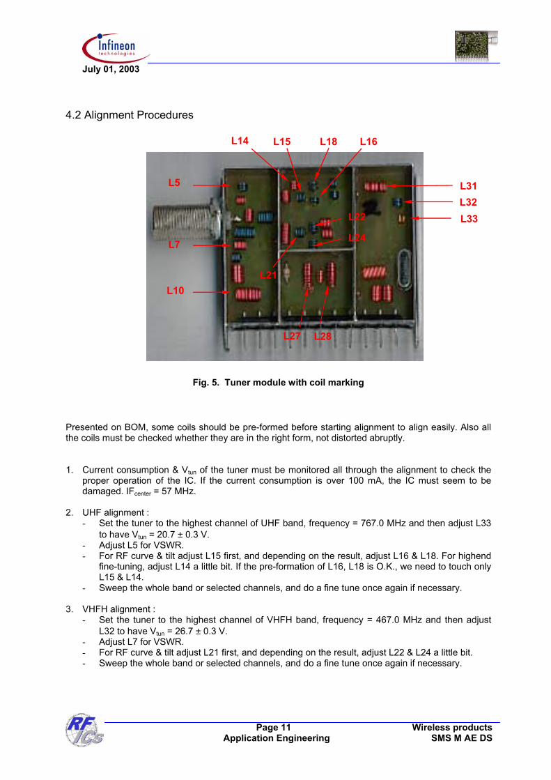
4.2 Alignment Procedures L14 L16L15 L18
L5
L33
L10
L7 L24
L22
L21
L28L27
L31L32
Fig. 5. Tuner module with coil marking
Presented on BOM, some coils should be pre-formed before starting alignment to align easily. Also all the coils must be checked whether they are in the right form, not distorted abruptly. 1. Current consumption & Vtun of the tuner must be monitored all through the alignment to check the
proper operation of the IC. If the current consumption is over 100 mA, the IC must seem to be damaged. IFcenter = 57 MHz.
2. UHF alignment :
- Set the tuner to the highest channel of UHF band, frequency = 767.0 MHz and then adjust L33 to have Vtun = 20.7 ± 0.3 V.
- Adjust L5 for VSWR. - For RF curve & tilt adjust L15 first, and depending on the result, adjust L16 & L18. For highend
fine-tuning, adjust L14 a little bit. If the pre-formation of L16, L18 is O.K., we need to touch only L15 & L14.
- Sweep the whole band or selected channels, and do a fine tune once again if necessary.
3. VHFH alignment : - Set the tuner to the highest channel of VHFH band, frequency = 467.0 MHz and then adjust
L32 to have Vtun = 26.7 ± 0.3 V. - Adjust L7 for VSWR. - For RF curve & tilt adjust L21 first, and depending on the result, adjust L22 & L24 a little bit. - Sweep the whole band or selected channels, and do a fine tune once again if necessary.
July 01, 2003
Page 12 Wireless products Application Engineering SMS M AE DS
4. VHFL alignment :
- Set the tuner to the highest channel of VHFL band, frequency = 167.0 MHz and then adjust L31 to have Vtun = 16 ± 0.3 V.
- Adjust L10 for VSWR. - For RF curve & tilt adjust L27 (main) & L28 a little bit. - Sweep the whole band or selected channels, and do a fine tune once again if necessary.
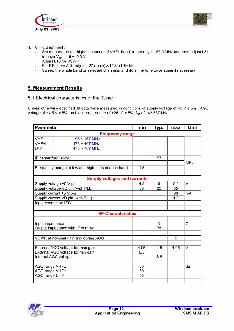
5. Measurement Results 5.1 Electrical characteristics of the Tuner Unless otherwise specified all data were measured in conditions of supply voltage of +5 V ± 5%, AGC voltage of +4.5 V ± 5%, ambient temperature of +25 ºC ± 5%, fref of 142.857 kHz.
Parameter min typ. max Unit Frequency range
VHFL 93 ~ 167 MHz VHFH 173 ~ 467 MHz UHF 473 ~ 767 MHz IF center frequency 57 Frequency margin at low and high ends of each band 1.5
MHz
Supply voltages and currents
Supply voltage +5 V pin 4.5 5 5.5 Supply voltage VD pin (with PLL) 30 33 35
V
Supply current +5 V pin 90 Supply current VD pin (with PLL) 1.8
mA
Input connector: IEC
RF Characteristics Input impedance Output impedance with IF dummy
75 75
Ω
VSWR at nominal gain and during AGC 5 External AGC voltage for max gain External AGC voltage for min gain Internal AGC voltage
4.05 0.5
4.5
3.8
4.95 V
AGC range VHFL AGC range VHFH AGC range UHF
60 60 50
dB
July 01, 2003
Page 13 Wireless products Application Engineering SMS M AE DS
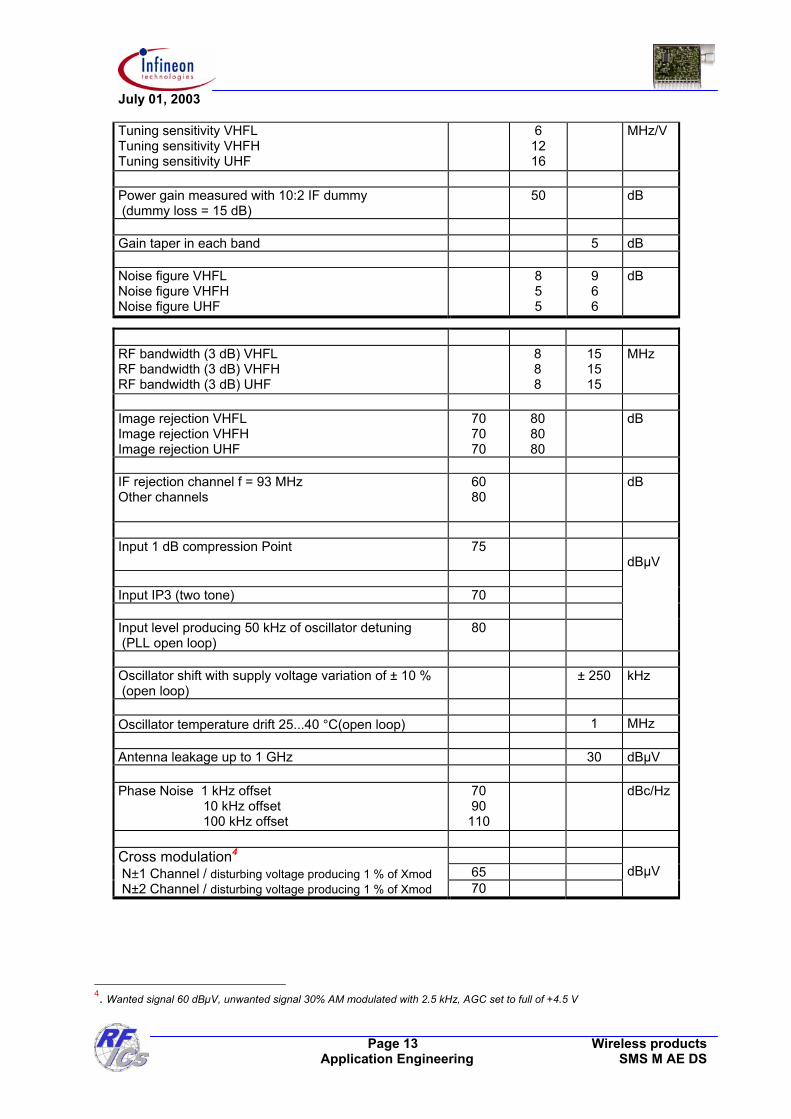
Tuning sensitivity VHFL Tuning sensitivity VHFH Tuning sensitivity UHF
6 12 16
MHz/V
Power gain measured with 10:2 IF dummy (dummy loss = 15 dB)
50 dB
Gain taper in each band 5 dB Noise figure VHFL Noise figure VHFH Noise figure UHF
8 5 5
9 6 6
dB
RF bandwidth (3 dB) VHFL RF bandwidth (3 dB) VHFH RF bandwidth (3 dB) UHF
8 8 8
15 15 15
MHz
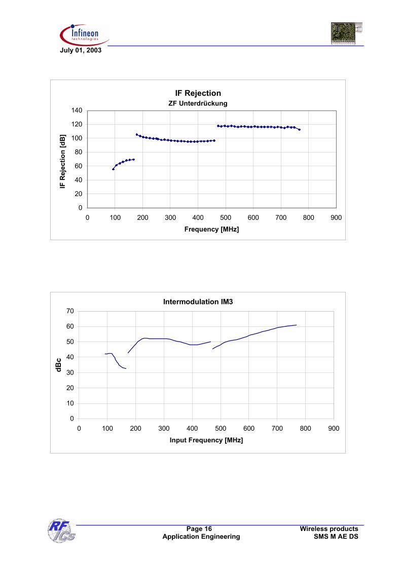
Image rejection VHFL Image rejection VHFH Image rejection UHF
70 70 70
80 80 80
dB
IF rejection channel f = 93 MHz Other channels
60 80
dB
Input 1 dB compression Point 75
Input IP3 (two tone) 70 Input level producing 50 kHz of oscillator detuning (PLL open loop)
80
dBµV
Oscillator shift with supply voltage variation of ± 10 % (open loop)
± 250 kHz
Oscillator temperature drift 25...40 °C(open loop) 1 MHz Antenna leakage up to 1 GHz 30 dBµV Phase Noise 1 kHz offset 10 kHz offset 100 kHz offset
70 90 110
dBc/Hz
65 dBµV
Cross modulation4 N±1 Channel / disturbing voltage producing 1 % of Xmod N±2 Channel / disturbing voltage producing 1 % of Xmod 70
4. Wanted signal 60 dBµV, unwanted signal 30% AM modulated with 2.5 kHz, AGC set to full of +4.5 V
July 01, 2003
Page 14 Wireless products Application Engineering SMS M AE DS
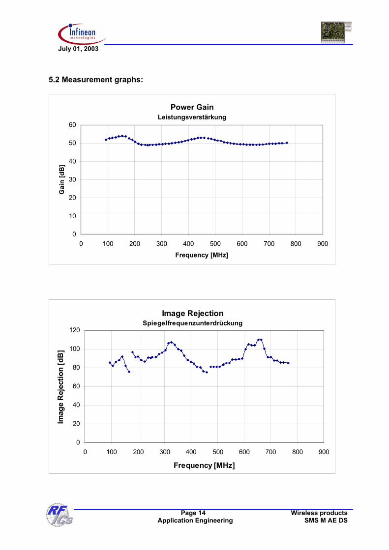
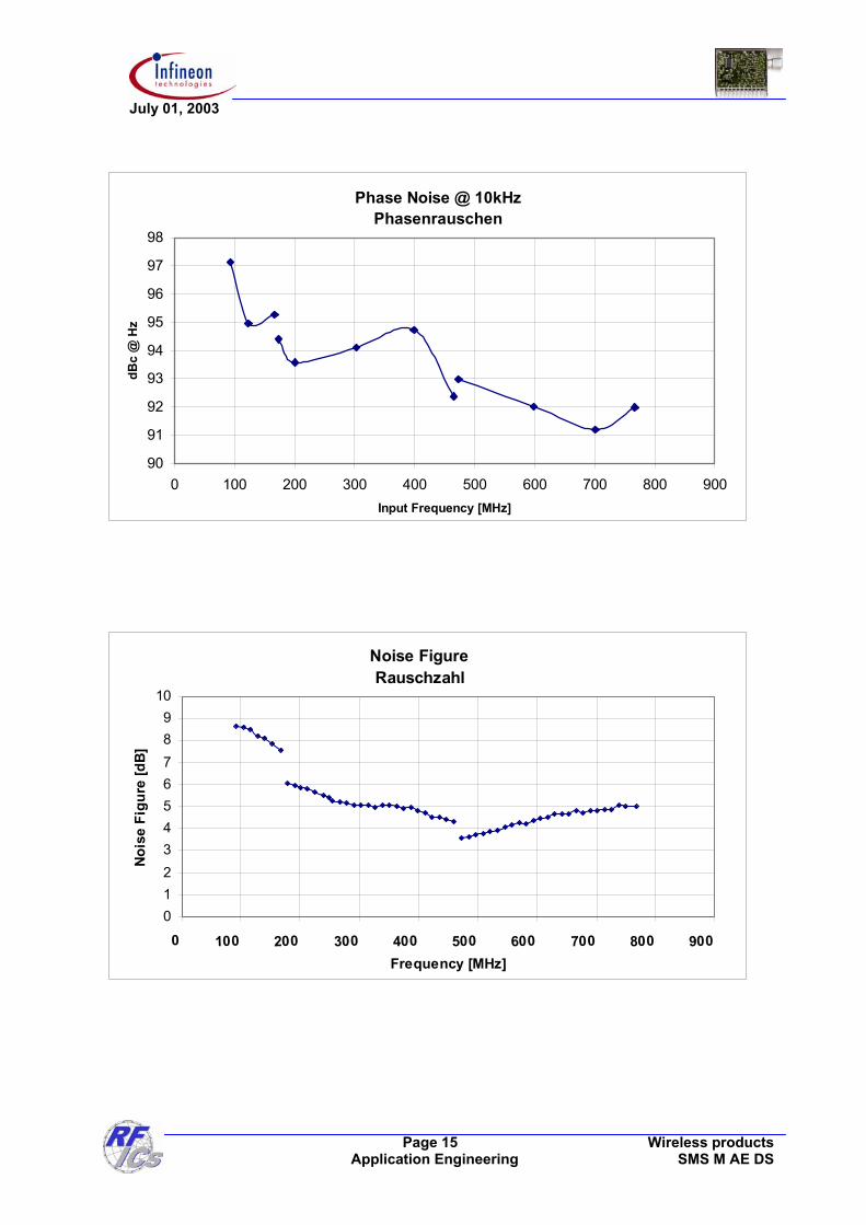
5.2 Measurement graphs:
Power GainLeistungsverstärkung
0
10
20
30
40
50
60
0 100 200 300 400 500 600 700 800 900
Frequency [MHz]
Gai
n [d
B]
Image RejectionSpiegelfrequenzunterdrückung
0
20
40
60
80
100
120
0 100 200 300 400 500 600 700 800 900
Frequency [MHz]
Imag
e R
ejec
tion
[dB
]
July 01, 2003
Page 15 Wireless products Application Engineering SMS M AE DS
Phase Noise @ 10kHz Phasenrauschen
90
91
92
93
94
95
96
97
98
0 100 200 300 400 500 600 700 800 900Input Frequency [MHz]
dBc
@ H
z
Noise FigureRauschzahl
0123456789
10
0 100 200 300 400 500 600 700 800 900Frequency [MHz]
Nois
e Fi
gure
[dB]
July 01, 2003
Page 16 Wireless products Application Engineering SMS M AE DS
IF RejectionZF Unterdrückung
0
20
40
60
80
100
120
140
0 100 200 300 400 500 600 700 800 900
Frequency [MHz]
IF R
ejec
tion
[dB]
Intermodulation IM3
0
10
20
30
40
50
60
70
0 100 200 300 400 500 600 700 800 900
Input Frequency [MHz]
dBc

July 01, 2003
Page 17 Wireless products Application Engineering SMS M AE DS
Input IP3Interceptpunkt 3. Ordnung
0102030405060708090
0 100 200 300 400 500 600 700 800 900
Frequency [MHz]
Inpu
t IP3
[dB
µV]
1 dB Compression1 dB Kompression
60
70
80
90
100
110
120
130
0 100 200 300 400 500 600 700 800 900
Frequency [MHz]
Inpu
t/Out
put L
evel
[d
BµV]
Input Pow er [dBµ]
Output Pow er [dBµ]
July 01, 2003
Page 18 Wireless products Application Engineering SMS M AE DS
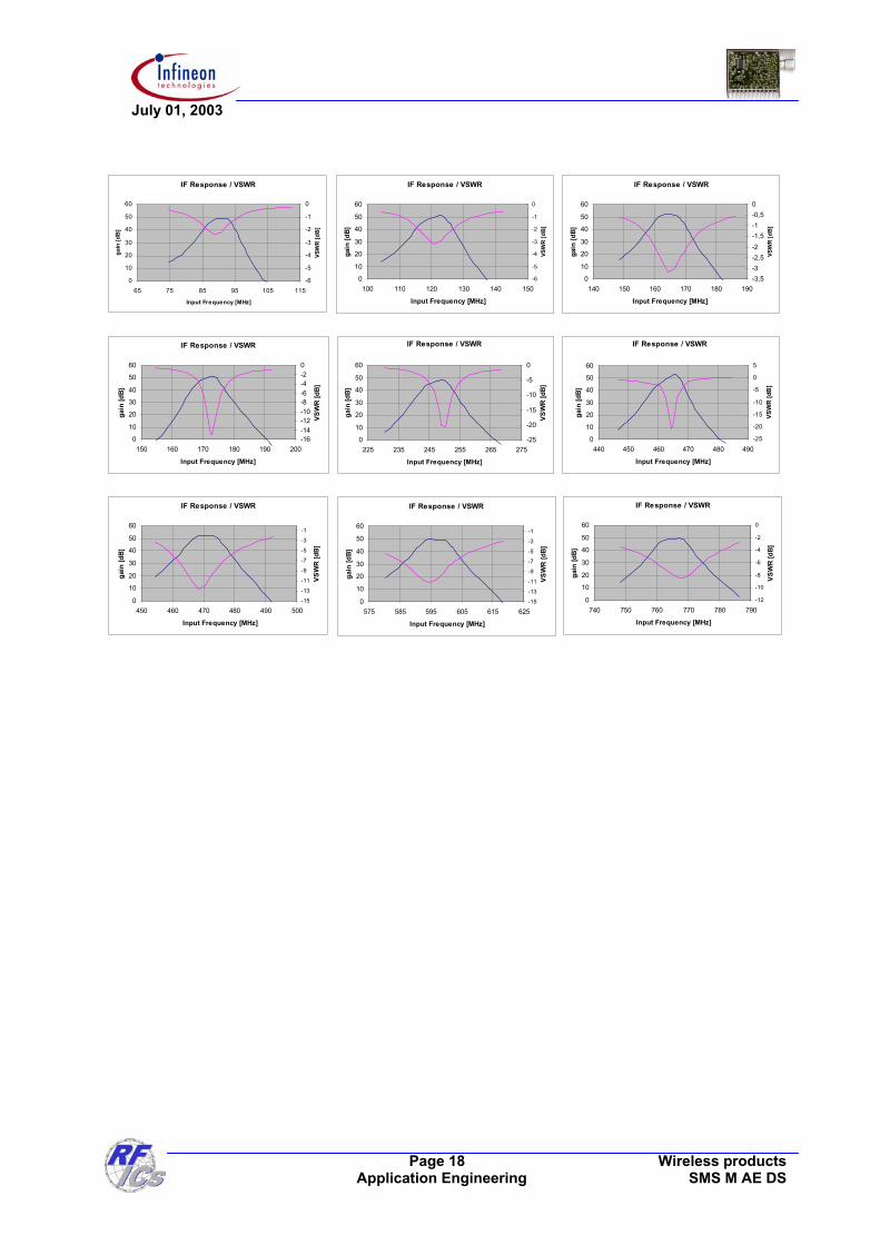
IF Response / VSWR
0
10
20
30
40
50
60
65 75 85 95 105 115
Input Frequency [MHz]
gain
[dB
]
-6
-5
-4
-3
-2
-1
0
VSW
R [d
B]
IF Response / VSWR
0
10
20
30
40
50
60
100 110 120 130 140 150
Input Frequency [MHz]
gain
[dB]
-6
-5
-4
-3
-2
-1
0
VSW
R [d
B]
IF Response / VSWR
0
10
20
30
40
50
60
140 150 160 170 180 190
Input Frequency [MHz]
gain
[dB]
-3,5-3-2,5-2-1,5-1-0,50
VSW
R [d
B]
IF Response / VSWR
0
10
20
30
40
50
60
150 160 170 180 190 200
Input Frequency [MHz]
gain
[dB]
-16-14-12-10-8-6-4-20
VSW
R [d
B]
IF Response / VSWR
0
10
20
30
40
50
60
225 235 245 255 265 275
Input Frequency [MHz]
gain
[dB]
-25
-20
-15
-10
-5
0
VSW
R [d
B]
IF Response / VSWR
0
10
20
30
40
50
60
440 450 460 470 480 490
Input Frequency [MHz]
gain
[dB]
-25
-20
-15
-10
-5
0
5
VSW
R [d
B]
IF Response / VSWR
0
10
20
30
40
50
60
450 460 470 480 490 500
Input Frequency [MHz]
gain
[dB]
-15
-13
-11
-9
-7
-5
-3
-1
VSW
R [d
B]
IF Response / VSWR
0
10
20
30
40
50
60
575 585 595 605 615 625
Input Frequency [MHz]
gain
[dB]
-15
-13
-11
-9
-7
-5
-3
-1
VSW
R [d
B]
IF Response / VSWR
0
10
20
30
40
50
60
740 750 760 770 780 790
Input Frequency [MHz]
gain
[dB]
-12
-10
-8
-6
-4
-2
0
VSW
R [d
B]

July 01, 2003
Page 19 Wireless products Application Engineering SMS M AE DS
AGC @ VHFL
-70-60-50-40-30-20-10
010
0 0,5 1 1,5 2 2,5 3 3,5 4 4,5 5
Vagc [V]
gain
[dB
]
AGC @ VHFH
-80-70-60-50-40-30-20-10
010
0 0,5 1 1,5 2 2,5 3 3,5 4 4,5 5
Vagc [V]
gain
[dB
]
AGC @ UHF
-70
-60-50
-40
-30
-20-10
0
10
0 0,5 1 1,5 2 2,5 3 3,5 4 4,5 5
Vagc [V]
gain
[dB
]
July 01, 2003
Page 20 Wireless products Application Engineering SMS M AE DS
Phase noise measurement results: Loopfilter parameter: C65=2n7; C68=56n; R39=22k; R40=1k; C24=22n
Phase noise VHF low, 93MHz
-140-130-120-110-100-90-80-70-60
0,1 1 10 100 1000 10000
delta f [kHz]
dBc
50µA 250µA 650µA
Phase noise VHF low, 129MHz
-140-130-120-110-100-90-80-70-60
0,1 1 10 100 1000 10000
delta f [kHz]
dBc
50µA 250µA 650µA
Phase noise VHF low, 167MHz
-140
-130
-120
-110-100
-90
-80
-70
-60
0,1 1 10 100 1000 10000
delta f [kHz]
dBc
50µA 250µA 650µA

July 01, 2003
Page 21 Wireless products Application Engineering SMS M AE DS
Phase noise VHF high, 173MHz
-140
-130
-120
-110
-100
-90
-80
-70
-60
0,1 1 10 100 1000 10000
delta f [kHz]
dBc
50µA 125µA
Phase noise VHF high, 321MHz
-130
-120
-110
-100
-90
-80
-70
-60
0,1 1 10 100 1000 10000
delta f [kHz]
dBc
50µA 250µA 125µA
Phase noise VHF high, 465MHz
-140-130-120-110-100
-90-80-70-60
0,1 1 10 100 1000 10000
delta f [kHz]
dBc
50µA 250µA 650µA 125µA

July 01, 2003
Page 22 Wireless products Application Engineering SMS M AE DS
Phase noise UHF, 473MHz
-140-130-120-110-100-90-80-70-60
0,1 1 10 100 1000 10000
delta f [kHz]
dBc
50µA 250µA 650µA
Phase noise UHF, 623MHz
-140
-130
-120
-110
-100
-90
-80
-70
-60
0,1 1 10 100 1000 10000
delta f [kHz]
dBc
50µA 250µA 650µA
Phase noise UHF, 767MHz
-140-130-120-110-100-90-80-70-60
0,1 1 10 100 1000 10000
delta f [kHz]
dBc
50µA 250µA 650µA
July 01, 2003
Page 23 Wireless products Application Engineering SMS M AE DS
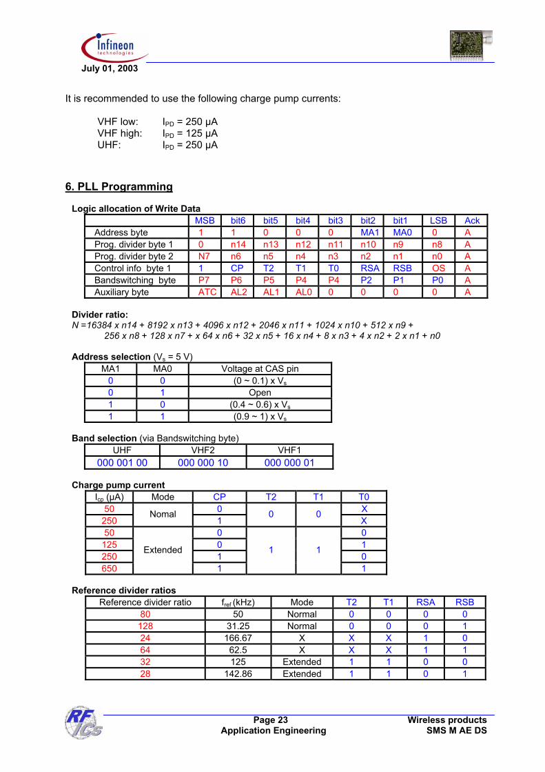
It is recommended to use the following charge pump currents: VHF low: IPD = 250 µA VHF high: IPD = 125 µA UHF: IPD = 250 µA
6. PLL Programming
Logic allocation of Write Data MSB bit6 bit5 bit4 bit3 bit2 bit1 LSB Ack Address byte 1 1 0 0 0 MA1 MA0 0 A Prog. divider byte 1 0 n14 n13 n12 n11 n10 n9 n8 A Prog. divider byte 2 N7 n6 n5 n4 n3 n2 n1 n0 A Control info byte 1 1 CP T2 T1 T0 RSA RSB OS A Bandswitching byte P7 P6 P5 P4 P4 P2 P1 P0 A Auxiliary byte ATC AL2 AL1 AL0 0 0 0 0 A
Divider ratio: N =16384 x n14 + 8192 x n13 + 4096 x n12 + 2046 x n11 + 1024 x n10 + 512 x n9 + 256 x n8 + 128 x n7 + x 64 x n6 + 32 x n5 + 16 x n4 + 8 x n3 + 4 x n2 + 2 x n1 + n0 Address selection (Vs = 5 V)
MA1 MA0 Voltage at CAS pin 0 0 (0 ~ 0.1) x Vs 0 1 Open 1 0 (0.4 ~ 0.6) x Vs 1 1 (0.9 ~ 1) x Vs
Band selection (via Bandswitching byte)
UHF VHF2 VHF1 000 001 00 000 000 10 000 000 01
Charge pump current
Icp (µA) Mode CP T2 T1 T0 50 0 X
250 Nomal
1 0 0
X 50 0 0
125 0 1 250 1 0 650
Extended
1
1 1
1 Reference divider ratios
Reference divider ratio fref (kHz) Mode T2 T1 RSA RSB 80 50 Normal 0 0 0 0 128 31.25 Normal 0 0 0 1 24 166.67 X X X 1 0 64 62.5 X X X 1 1 32 125 Extended 1 1 0 0 28 142.86 Extended 1 1 0 1
July 01, 2003
Page 24 Wireless products Application Engineering SMS M AE DS
The Tuner PLL control software, WinPLL is also available along with the evaluation board & the reference tuner.
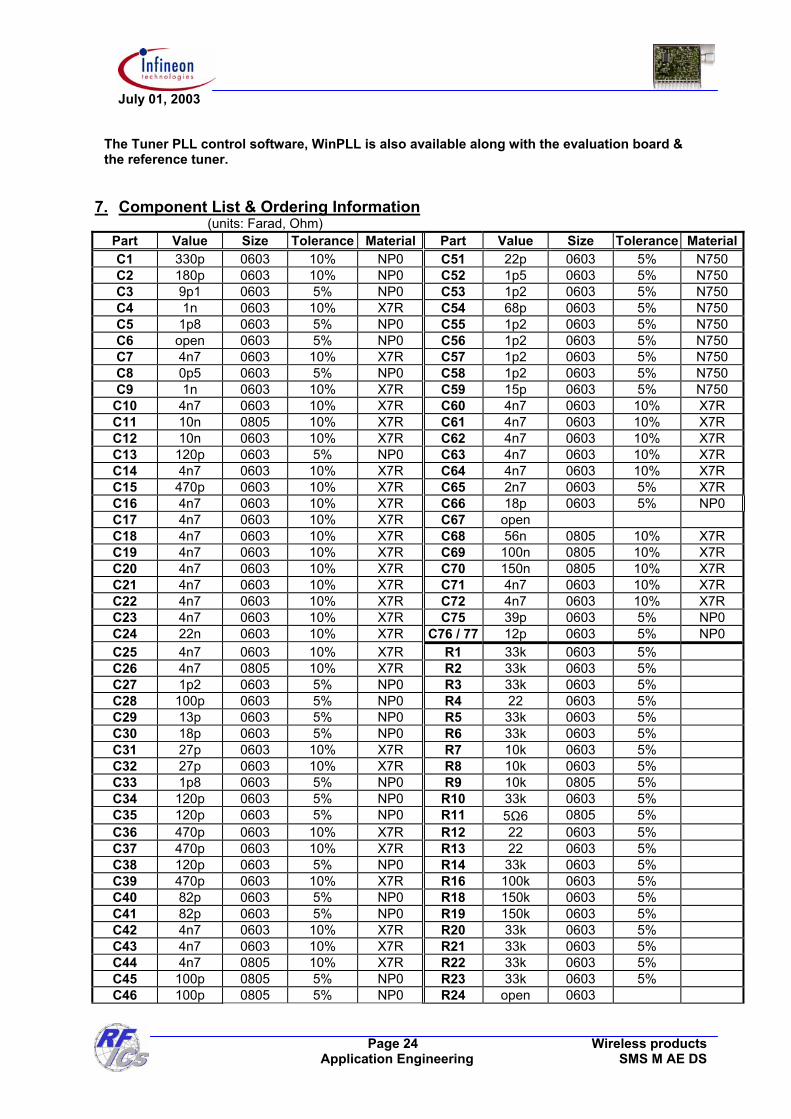
7. Component List & Ordering Information (units: Farad, Ohm)
Part Value Size Tolerance Material Part Value Size Tolerance MaterialC1 330p 0603 10% NP0 C51 22p 0603 5% N750 C2 180p 0603 10% NP0 C52 1p5 0603 5% N750 C3 9p1 0603 5% NP0 C53 1p2 0603 5% N750 C4 1n 0603 10% X7R C54 68p 0603 5% N750 C5 1p8 0603 5% NP0 C55 1p2 0603 5% N750 C6 open 0603 5% NP0 C56 1p2 0603 5% N750 C7 4n7 0603 10% X7R C57 1p2 0603 5% N750 C8 0p5 0603 5% NP0 C58 1p2 0603 5% N750 C9 1n 0603 10% X7R C59 15p 0603 5% N750
C10 4n7 0603 10% X7R C60 4n7 0603 10% X7R C11 10n 0805 10% X7R C61 4n7 0603 10% X7R C12 10n 0603 10% X7R C62 4n7 0603 10% X7R C13 120p 0603 5% NP0 C63 4n7 0603 10% X7R C14 4n7 0603 10% X7R C64 4n7 0603 10% X7R C15 470p 0603 10% X7R C65 2n7 0603 5% X7R C16 4n7 0603 10% X7R C66 18p 0603 5% NP0 C17 4n7 0603 10% X7R C67 open C18 4n7 0603 10% X7R C68 56n 0805 10% X7R C19 4n7 0603 10% X7R C69 100n 0805 10% X7R C20 4n7 0603 10% X7R C70 150n 0805 10% X7R C21 4n7 0603 10% X7R C71 4n7 0603 10% X7R C22 4n7 0603 10% X7R C72 4n7 0603 10% X7R C23 4n7 0603 10% X7R C75 39p 0603 5% NP0 C24 22n 0603 10% X7R C76 / 77 12p 0603 5% NP0 C25 4n7 0603 10% X7R R1 33k 0603 5% C26 4n7 0805 10% X7R R2 33k 0603 5% C27 1p2 0603 5% NP0 R3 33k 0603 5% C28 100p 0603 5% NP0 R4 22 0603 5% C29 13p 0603 5% NP0 R5 33k 0603 5% C30 18p 0603 5% NP0 R6 33k 0603 5% C31 27p 0603 10% X7R R7 10k 0603 5% C32 27p 0603 10% X7R R8 10k 0603 5% C33 1p8 0603 5% NP0 R9 10k 0805 5% C34 120p 0603 5% NP0 R10 33k 0603 5% C35 120p 0603 5% NP0 R11 5Ω6 0805 5% C36 470p 0603 10% X7R R12 22 0603 5% C37 470p 0603 10% X7R R13 22 0603 5% C38 120p 0603 5% NP0 R14 33k 0603 5% C39 470p 0603 10% X7R R16 100k 0603 5% C40 82p 0603 5% NP0 R18 150k 0603 5% C41 82p 0603 5% NP0 R19 150k 0603 5% C42 4n7 0603 10% X7R R20 33k 0603 5% C43 4n7 0603 10% X7R R21 33k 0603 5% C44 4n7 0805 10% X7R R22 33k 0603 5% C45 100p 0805 5% NP0 R23 33k 0603 5% C46 100p 0805 5% NP0 R24 open 0603

July 01, 2003
Page 25 Wireless products Application Engineering SMS M AE DS
C47 4n7 0805 10% X7R R25 2Ω7 0603 5% C48 560p 0603 10% X7R R26 0 0603 C49 2p7 0603 5% N750 R27 open 0603 5% C50 2p2 0603 5% N750 R28 33k 0603 5%
Part Value Size Tolerance Part Turns D.of Wire D. of Coil Direction Pre-form.R29 330 0603 5% L1 12 0,4 2,2 CW R30 330 0603 5% L2 9 0,4 2,5 CW R31 12 0603 5% L3 9 0,3 2 CW R32 2k2 0805 5% L4 6 0,4 1,8 CCW R33 8Ω2 0603 5% L5 3 0,4 2,4 CW R34 2k7 0603 5% L6 printed R35 5Ω6 0603 5% L7 9 0,3 2 CCW R36 1k8 0603 5% L8 5 0,4 1,9 CW R37 1k8 0603 5% L9 12 0,3 3 CW R38 open L10 16 0,3 2,5 CW R39 22k 0603 5% L11 7 0,3 2 CW R40 1k 0805 5% L12 15 0,3 1,9 CW R42 1k2 0603 5% L13 choke coil L = 3.9uH R41 15 0603 5% L14 5 0,3 1,7 CCW R15 10k 0603 5% L15 3 0,4 1,9 CCW 0,5mm R17 15 0603 5% L16 2 0,5 1,6 CW 1,0mm J1 0 0603 L17 printed J2 0 0805 L18 2 0,5 1,6 CCW J3 0 0805 L19 4 0,4 1,9 CW J4 0 0805 L20 4 0,4 1,9 CW J5 0 0603 L21 4 0,4 1,9 CW J6 0 0603 L22 4 0,4 1,5 CW J7 0 0805 L23 printed J8 0 0805 L24 4 0,4 1,6 CCW J9 0 0805 L25 8 0,3 2 CCW
J10 0 0805 L26 8 0,3 2 CW J12 0 0603 L27 13 0,3 2,2 CW
L36 / 37 150nH 0805 LQG21NR L28 13 0,3 2,2 CW 15K10 L29 7 0,3 2 CCW Murata L31 9 0,3 2,2 CW L32 2,5 0,5 2,4 CW 0,5mm L33 1,5 0,4 1,9 CW L34 11 0,3 2,3 CW L35 11 0,3 2,3 CW
full-turn, CCW:
July 01, 2003
Page 26 Wireless products Application Engineering SMS M AE DS
Note1) All the coils are full-turn types. The unit of the diameter of coil & wire is 'mm'. Note2) J1 & C70 are only for internal tuner AGC. Note3) Pre-form. value is the distance between each turn of the coils. The pre-formation of
coils should be done before alignment by a coil manufacturer or by line workers.
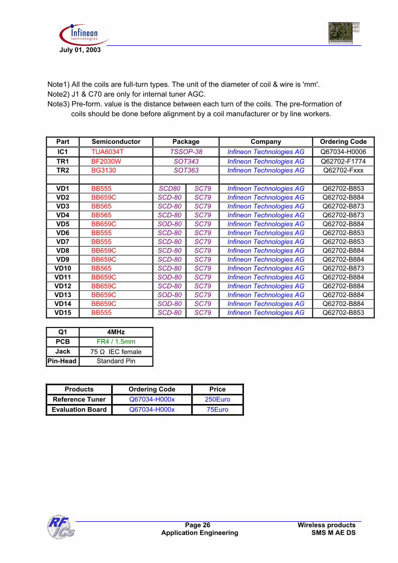
Part Semiconductor Package Company Ordering Code IC1 TUA6034T TSSOP-38 Infineon Technologies AG Q67034-H0006 TR1 BF2030W SOT343 Infineon Technologies AG Q62702-F1774 TR2 BG3130 SOT363 Infineon Technologies AG Q62702-Fxxx
VD1 BB555 SCD80 SC79 Infineon Technologies AG Q62702-B853 VD2 BB659C SCD-80 SC79 Infineon Technologies AG Q62702-B884 VD3 BB565 SCD-80 SC79 Infineon Technologies AG Q62702-B873 VD4 BB565 SCD-80 SC79 Infineon Technologies AG Q62702-B873 VD5 BB659C SOD-80 SC79 Infineon Technologies AG Q62702-B884 VD6 BB555 SCD-80 SC79 Infineon Technologies AG Q62702-B853 VD7 BB555 SCD-80 SC79 Infineon Technologies AG Q62702-B853 VD8 BB659C SCD-80 SC79 Infineon Technologies AG Q62702-B884 VD9 BB659C SCD-80 SC79 Infineon Technologies AG Q62702-B884 VD10 BB565 SCD-80 SC79 Infineon Technologies AG Q62702-B873 VD11 BB659C SOD-80 SC79 Infineon Technologies AG Q62702-B884 VD12 BB659C SCD-80 SC79 Infineon Technologies AG Q62702-B884 VD13 BB659C SOD-80 SC79 Infineon Technologies AG Q62702-B884 VD14 BB659C SOD-80 SC79 Infineon Technologies AG Q62702-B884 VD15 BB555 SCD-80 SC79 Infineon Technologies AG Q62702-B853
Q1 4MHz
PCB FR4 / 1.5mm Jack 75 Ω IEC female
Pin-Head Standard Pin
Products Ordering Code Price
Reference Tuner Q67034-H000x 250Euro Evaluation Board Q67034-H000x 75Euro
July 01, 2003
Page 27 Wireless products Application Engineering SMS M AE DS
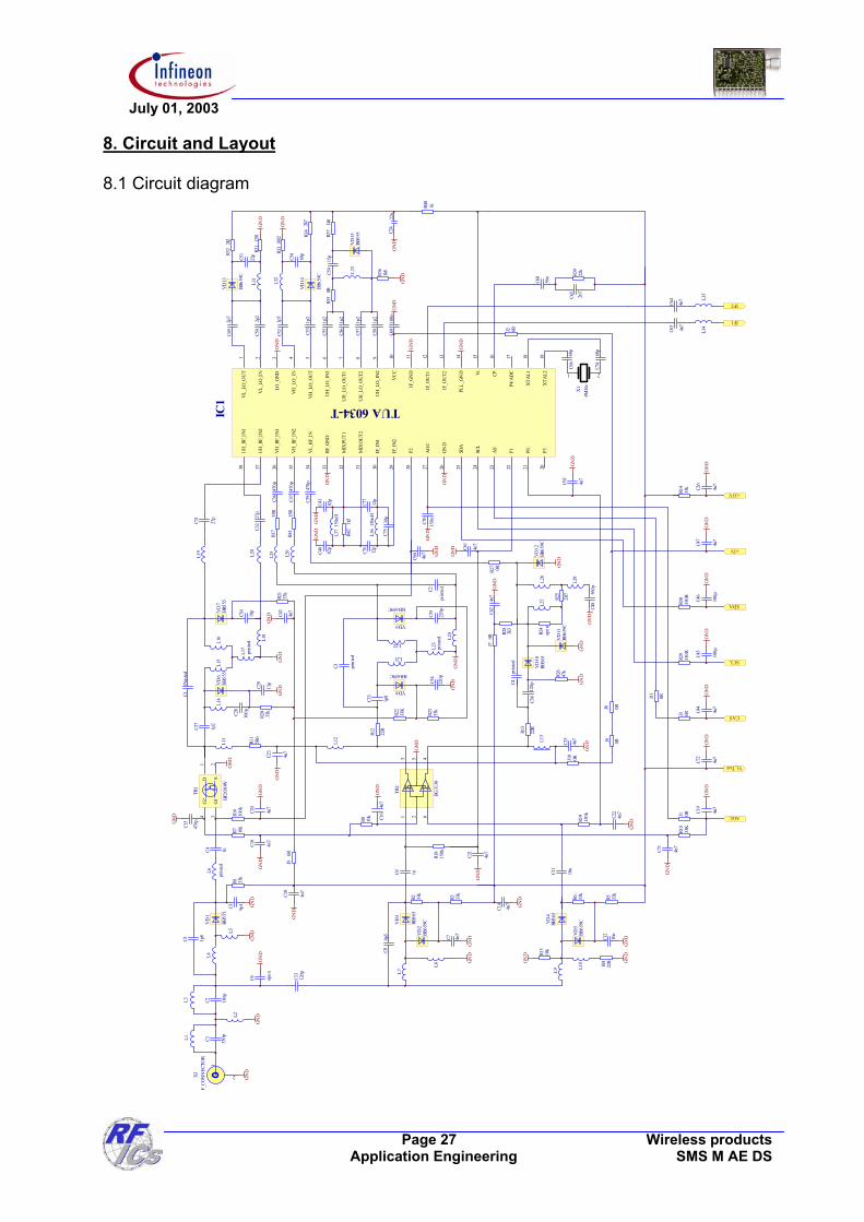
8. Circuit and Layout 8.1 Circuit diagram
R35
0R
L33
R37
1k8
R36
1k8
GN
DG
ND
GN
D
GN
D
GN
D
GN
D
GN
D
R34
2k7
R33
8R2
L32
GN
D
R31
12R
R32
2k2
L31
GN
D
R40
1k
C24
22n
GN
D
L34
L35
J2 0R
R39
22k
R17
15R
L25
R41
15R
L26
R42
1k5
L37
150
nH
GN
DG
ND
GN
D
GN
D
+33VR14
33k
GN
D
+5V
GN
D
SDAR30
330R
GN
D
SCLR29
330R
GN
D
CASJ3 0R
GN
D
Vt_Test
GN
D
AGCJ1 0R
GN
D
R10
33K
GN
D
R27 0R
L28
L27
L29
R25
2R7
R24
open
GN
D
GN
DG
ND
R28
3k3
GN
D
GN
D
R26
47k
GN
D
R13
22R
L13
GN
D
J10
0R
J9 0R
J8 0R
J70R
R23
33k
L21
L22
L23
prin
ted L2
4G
ND
GN
D
R22
33K
R12
22R
GN
DL12
R19
150k
GN
D
GN
D
R8 10k
R18
150k
GN
D
GN
D
L15
L16
L17
prin
ted
L19
L20
GN
DG
ND
L18
GN
D
R21
33k
L14
L11
R11
5R6
R20
33k
GN
D
D1
S2
G2
4
G1
3
TR1
BF20
30W
GN
DR1
610
0k
GN
D
R7 10k
GN
D
R1 33k
L6
prin
ted
GN
DG
ND
GN
DJ5
0R
L5
L4
GN
D
L7
L8
R2 33k
R3 33k
GN
DG
ND
GN
D
R6 33k
R5 33k
GN
D
R4 22R
R15
10k
L10
L9
GN
D
GN
D
L1L3
L2
GN
D
GN
D
2
1
X3
F_C
ON
NEC
TOR
1 2
X1
4MH
z
L36
150
nH
C40
82p
C76
12p
C77
12p
C75
39p
C41
82p
C70
150n
C49
2p7
IF_O
UT2
13
P320
GN
D26
SDA
25
SCL
24
AS
23
P122
P021
PLL
_GN
D14
Vt
15
CP16
P4/A
DC
17
XT
AL1
18
XT
AL2
19
UH
_LO
_IN
16
UH
_LO
_OU
T17
UH
_LO
_OU
T28
UH
_LO
_IN
29
VC
C10
IF_G
ND
11
IF_O
UT1
12
VL
_LO
_OU
T1
VL_L
O_I
N2
LO_G
ND
3
VH_L
O_I
N4
VH
_LO
_OU
T5
AG
C27
RF_G
ND
33
MIX
PUT
132
MIX
OU
T2
31
IF_I
N1
30
IF_I
N2
29
P228
VL
_RF_
IN34
UH
_RF_
IN1
38
UH
_RF_
IN2
37
VH
_RF_
IN1
36
VH
_RF_
IN2
35
IC1 TUA 6034-T
GN
D
C62
4n7
C50
2p2
C52
1p5
C51
22p
C53
1p2
C54
68p
C59
15p
C55
1p2
C56
1p2
C69
100n
C57
1p2
C58
1p2
C68
56n
C65
2n7
C66
68p
C74
68p
IF1
IF2
C63
4n7
C64
4n7
C31
27p
C32
27p
C30
18p
C1Pr
inte
d
C27
1p2
C28
100p
C29
13p
C43
4n7
C23
4n7
VD
7BB
555
C20
4n7
C18
4n7
C4 1n
C15
470p
C3 9p1
C5 1p8
C6 open
C2 180p
C1 330p
C80p
5
C13
120p
C14
4n7
C11
10n
C16
4n7
C12
10n
C22
4n7
C38
120pC4
prin
ted
C42
4n7
C61
4n7
C25
4n7
C48
560p
C39
470p
C60
4n7
C26
4n7
C47
4n7
C46
100p
C45
100p
C44
4n7
C72
4n7
C19
4n7
C71
4n7
C36
470p
C37
470p
VD
6BB
555
VD
1
BB55
5
C10
4n7
VD
3
BB56
5V
D2
BB65
9C
VD8
BB659C
VD9
BB659C
VD
12BB
659C
VD11
BB65
9C
VD
10BB
565
C7 4n7
C21
4n7
VD
4BB
565
VD
5BB
659C
VD
13
BB65
9C
VD
14
BB65
9C
VD15
BB55
5
C3 prin
ted
C33
1p8
C34
220p
C35
220p
C2
prin
ted
C9 1n
J11
0R
31 2 6
5 4
TR2
BG31
30
July 01, 2003
Page 28 Wireless products Application Engineering SMS M AE DS
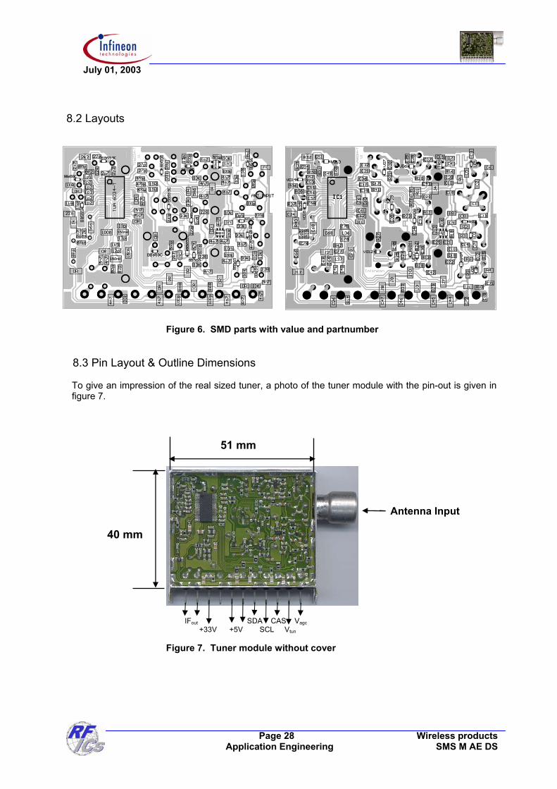
8.2 Layouts
Figure 6. SMD parts with value and partnumber 8.3 Pin Layout & Outline Dimensions To give an impression of the real sized tuner, a photo of the tuner module with the pin-out is given in figure 7.
51 mm
40 mm
Antenna Input
IFout SDA CAS Vagc +33V +5V SCL Vtun
Figure 7. Tuner module without cover
July 01, 2003
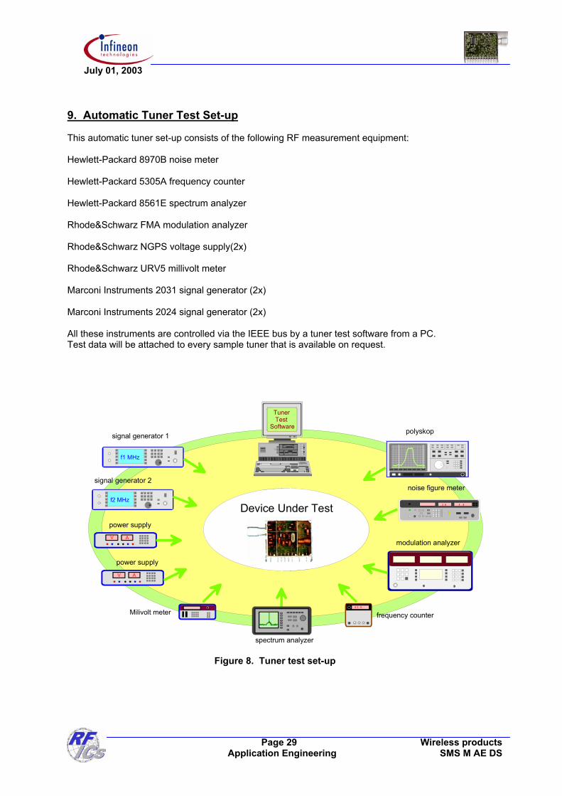
9. Automatic Tuner Test Set-up
his automatic tuner set-up consists of the following RF measurement equipment:
Hewlett-Packard 8970B noise meter Hewlett-Packard 5305A frequency counter Hewlett-Packard 8561E spectrum analyzer Rhode&Schwarz FMA modulation analyzer Rhode&Schwarz NGPS voltage supply(2x) Rhode&Schwarz URV5 millivolt meter Marconi Instruments 2031 signal generator (2x) Marconi Instruments 2024 signal generator (2x)
All these instruments ar from a PC. est data will be attached to every sample tuner that is available on request.
Figure 8. Tuner test set-up
T
e controlled via the IEEE bus by a tuner test software
T
f1 MHz
f2 MHz
gnal generator 2
modulation analyzer
power supply
V A
power supply
Tuner TestSoftware
er
signal generator 1
si
V A
spectrum analyz
4 . 83 8
noise figure meter
Milivolt meter frequency counter4 3 .
polyskop
Device Under Test
5
Page 29 Wireless products Application Engineering SMS M AE DS

July 01, 2003
Page 30 Wireless products Application Engineering SMS M AE DS
n10. Ordering & Contact Informatio
http://www.infineon.com/business/techlit/ordering/index.htm
1. Ordering on the Web
. For more information please contact our local sales colleagues in your region.
http://www.infineon.com/business/offices/index1.htm
2
Information on the Web 1. Infineon Homepage
http://www.infineon.com/
. Ordering Info
http://www.infineon.com/business/techlit/ordering/index.htm
2
3.
Analog & Digital Tuner ICs Info
http://www.infineon.com/cgi/ecrm.dll/ecrm/scripts/prod_cat.jsp?oid=-8036
Tuner MOSFETs & Varicap Diodes Info
http://www.infineon.com/cgi/ecrm.dll/ecrm/scripts/prod_ov.jsp?oid=26213&cat_oid=-8960 http://www.infineon.com/cgi/ecrm.dll/ecrm/scripts/prod_ov.jsp?oid=26227&cat_oid=-8960 http://www.infineon.com/cgi/ecrm.dll/ecrm/scripts/prod_ov.jsp?oid=26231&cat_oid=-8960 http://www.infineon.com/cgi/ecrm.dll/ecrm/scripts/prod_ov.jsp?oid=13798&cat_oid=-8148
4.

July 01, 2003
hnologies AG astenbauerstrasse 2 1677 München Infineon Technolog
Attention please! s far as patents or other rights of third parties are concerned, liability is only assumed for components, ot for applications, processes and circuits implemented within components or assemblies. he information describes the type of component and shall not be considered as assured
hange design reserved. ue to technical requirements components may contain dangerous substances. For information on the
ct your nearest Infineon Technologies Office. fineon Technologies AG is an approved CECC manufacturer.
Packing Please use the recycling operators known to you. We can also help you – get in touch with your nearest
ent we will take packing material back, if it is sorted. You must bear the costs of
or packing material that is returned to us unsorted or which we are not obliged to accept, we shall have to invoice you foComponents used in life-support devices or s st be expressly authorized for such purpose!
hnologies AG, may only be used in life-support devices or l of the Infineon Technologies AG.
1 co e failure can asonably be expected to cause the failure of that life-support device or system, or to affect its safety
r effectiveness of that device or system.
port devices or systems are intended (a) to be implanted in the human body, or (b) to support and/or e user may be
Edition July 2003 Published by Infineon TecK8© ies AG All rights reserved.
AnTcharacteristics. Terms of delivery and rights to cDtypes in question please contaIn
sales office. By agreemtransport. F
r any costs incurred. ystems mu
Critical components 1 of the Infineon Tecystems 2 with the express written approvas
A critical re
mponent is a component used in a life-support device or system whos
o
2 Life supmaintain and sustain human life. If they fail, it is reasonable to assume that the health of th endangered.
Page 31 Wireless products Application Engineering SMS M AE DS