apollo2 mcu datasheet - ambiq...
TRANSCRIPT

Apollo2 Datasheet
Apollo2 MCU Datasheet
Doc. ID: DS-A2-0p92
Revision 0.92
May 2017
DS-A2-0p92 Page 1 of 537 2017 Ambiq Micro, Inc.All rights reserved.
Apollo2 Datasheet
Ultra-Low Power MCU Family
FeaturesUltra-low supply current:
- < 10 µA/MHz executing from flash at 3.3 V- < 10 µA/MHz executing from RAM at 3.3 V- < 3 µA deep sleep mode with RTC at 3.3 V
High-performance ARM Cortex-M4 Processor- Up to 48 MHz clock frequency- Floating point unit- Memory protection unit- Wake-up interrupt controller with 32 interrupts
Ultra-low power memory:
- Up to 1 MB of flash memory for code/data- Up to 256 KB of low leakage RAM for code/data- 16kB 2-way Associative Cache
Ultra-low power interface for off-chip sensors:- 14 bit ADC at up to 1.2 MS/s, 11 simultaneous
input channels available- Voltage Comparator- Temperature sensor with +/-3ºC accuracy
Flexible serial peripherals:
- 6x I2C/SPI masters with 128-byte bidirectional FIFO for communication with sensors, radios, and other peripherals
- 1x I2C/SPI slave for host communications with 256-byte LRAM area for FIFO/host support
- 2x UART modules with 32-location transmit and receive FIFOs
- PDM for mono and stereo audio microphone (256-word FIFO)
- 1x I2S slave for PDM audio pass-through
Rich set of clock sources:- 32.768 kHz XTAL oscillator- Low frequency RC oscillator – 1.024 kHz- High frequency RC oscillator – 48 MHz- RTC based on Ambiq’s AM08X5/18X5 families
W
Co--
A-----
DThhigbaelesecoCoAptaslifeacgeAppa(Sin
Thbufamflaradof alscoac
DS-A2-0p92 Page
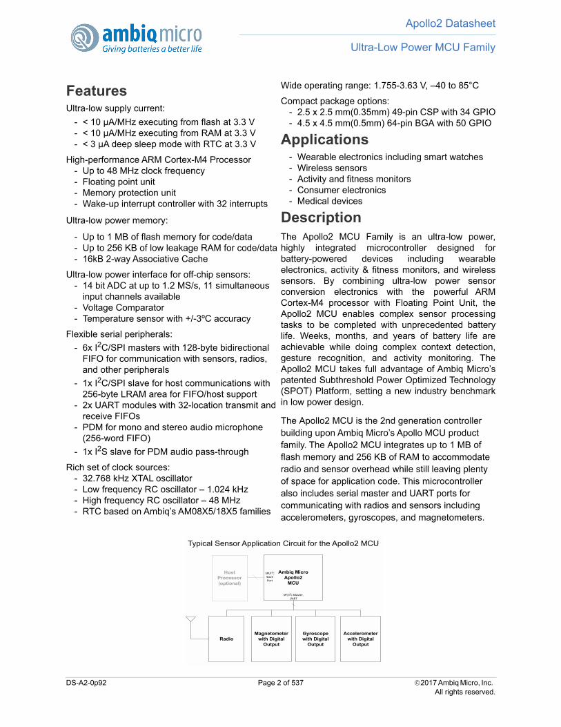
Host Processor(optional)
SPI/I2
SlavePort
RadioMagneto
with DOutp
Typical Sensor Applicatio
ide operating range: 1.755-3.63 V, –40 to 85°C
mpact package options:2.5 x 2.5 mm(0.35mm) 49-pin CSP with 34 GPIO4.5 x 4.5 mm(0.5mm) 64-pin BGA with 50 GPIO
pplicationsWearable electronics including smart watchesWireless sensorsActivity and fitness monitorsConsumer electronics Medical devices
escriptione Apollo2 MCU Family is an ultra-low power,hly integrated microcontroller designed forttery-powered devices including wearablectronics, activity & fitness monitors, and wirelessnsors. By combining ultra-low power sensornversion electronics with the powerful ARMrtex-M4 processor with Floating Point Unit, theollo2 MCU enables complex sensor processingks to be completed with unprecedented battery. Weeks, months, and years of battery life arehievable while doing complex context detection,sture recognition, and activity monitoring. Theollo2 MCU takes full advantage of Ambiq Micro’stented Subthreshold Power Optimized TechnologyPOT) Platform, setting a new industry benchmarklow power design.
e Apollo2 MCU is the 2nd generation controller ilding upon Ambiq Micro’s Apollo MCU product
ily. The Apollo2 MCU integrates up to 1 MB of sh memory and 256 KB of RAM to accommodate io and sensor overhead while still leaving plenty
space for application code. This microcontroller o includes serial master and UART ports for mmunicating with radios and sensors including celerometers, gyroscopes, and magnetometers.
2 of 537 2017 Ambiq Micro, Inc. All rights reserved.
Ambiq MicroApollo2
MCU
C
SPI/I2C Master,UART
meter igital ut
Gyroscope with Digital
Output
Accelerometer with Digital
Output
n Circuit for the Apollo2 MCU
Apollo2 Datasheet
Table of Content
1. Apollo2 MCU Package Pins .............................................................................................. 291.1 Pin Configuration ....................................................................................................... 291.2 Pin Connections ......................................................................................................... 31
2. System Core ....................................................................................................................... 523. MCU Core Details ............................................................................................................. 54
3.1 Interrupts .................................................................................................................... 543.2 Memory Map ............................................................................................................. 563.3 Memory Protection Unit (MPU) ................................................................................ 593.4 System Busses ............................................................................................................ 593.5 Power Management ................................................................................................... 59
3.5.1 Cortex M4 Power Modes .................................................................................. 603.5.2 System Power Modes ........................................................................................ 613.5.3 Power Control ................................................................................................... 62
3.6 Debug Interfaces ........................................................................................................ 713.6.1 Debugger Attachment ....................................................................................... 713.6.2 Instrumentation Trace Macrocell (ITM) ........................................................... 713.6.3 Trace Port Interface Unit (TPIU) ...................................................................... 723.6.4 Faulting Address Trapping Hardware ............................................................... 72
3.7 ITM Registers ............................................................................................................ 723.7.1 Register Memory Map ...................................................................................... 733.7.2 ITM Registers ................................................................................................... 75
3.8 MCUCTRL Registers .............................................................................................. 1003.8.1 Register Memory Map .................................................................................... 1013.8.2 MCUCTRL Registers ..................................................................................... 102
3.9 Memory Subsystem ................................................................................................. 1203.9.1 Features ........................................................................................................... 1203.9.2 Functional Overview ....................................................................................... 1213.9.3 Flash Cache ..................................................................................................... 1223.9.4 SRAM Interface .............................................................................................. 134
4. I2C/SPI Master Module ................................................................................................... 1364.1 Functional Overview ................................................................................................ 1364.2 Interface Clock Generation ...................................................................................... 1364.3 Command Operation ................................................................................................ 1374.4 FIFO ......................................................................................................................... 1394.5 I2C Interface ............................................................................................................ 139
4.5.1 Bus Not Busy .................................................................................................. 1404.5.2 Start Data Transfer .......................................................................................... 1404.5.3 Stop Data Transfer .......................................................................................... 1404.5.4 Data Valid ....................................................................................................... 1404.5.5 Acknowledge .................................................................................................. 1404.5.6 I2C Slave Addressing ..................................................................................... 1414.5.7 I2C Offset Address Transmission ................................................................... 1414.5.8 I2C Normal Write Operation .......................................................................... 1424.5.9 I2C Normal Read Operation ........................................................................... 142
DS-A2-0p92 Page 3 of 537 2017 Ambiq Micro, Inc.All rights reserved.
Apollo2 Datasheet
4.5.10 I2C Raw Write Operation ............................................................................. 1434.5.11 I2C Raw Read Operation .............................................................................. 1434.5.12 Holding the Interface with CONT ................................................................ 1434.5.13 I2C Multi-master Arbitration ........................................................................ 143
4.6 SPI Operations ......................................................................................................... 1444.6.1 SPI Configuration ........................................................................................... 1444.6.2 SPI Slave Addressing ...................................................................................... 1444.6.3 SPI Normal Write ........................................................................................... 1444.6.4 SPI Normal Read ............................................................................................ 1454.6.5 SPI Raw Write ................................................................................................ 1454.6.6 SPI Raw Read ................................................................................................. 1464.6.7 SPI 3-wire Mode ............................................................................................. 1464.6.8 Complex SPI Operations ................................................................................ 1464.6.9 SPI Polarity and Phase .................................................................................... 147
4.7 Repeating a Command ............................................................................................. 1474.8 Bit Orientation ......................................................................................................... 1484.9 Full Duplex Operations ............................................................................................ 1484.10 SPI Flow Control ................................................................................................... 1484.11 Pre-read Control ..................................................................................................... 1504.12 Minimizing Power ................................................................................................. 1514.13 IOMSTR Registers ................................................................................................ 151
4.13.1 Register Memory Map .................................................................................. 1524.13.2 IOMSTR Registers ....................................................................................... 154
5. I2C/SPI Slave Module ..................................................................................................... 1685.1 Functional Overview ................................................................................................ 1685.2 Local RAM Allocation ............................................................................................ 1685.3 Direct Area Functions .............................................................................................. 1695.4 FIFO Area Functions ............................................................................................... 1725.5 Rearranging the FIFO .............................................................................................. 1735.6 Interface Interrupts ................................................................................................... 1735.7 Command Completion Interrupts ............................................................................ 1745.8 Host Address Space and Registers ........................................................................... 1755.9 I2C Interface ............................................................................................................ 175
5.9.1 Bus Not Busy .................................................................................................. 1755.9.2 Start Data Transfer .......................................................................................... 1755.9.3 Stop Data Transfer .......................................................................................... 1755.9.4 Data Valid ....................................................................................................... 1765.9.5 Acknowledge .................................................................................................. 1765.9.6 Address Operation .......................................................................................... 1765.9.7 Offset Address Transmission .......................................................................... 1775.9.8 Write Operation .............................................................................................. 1775.9.9 Read Operation ............................................................................................... 1775.9.10 General Address Detection ........................................................................... 178
5.10 SPI Interface .......................................................................................................... 1785.10.1 Write Operation ............................................................................................ 1785.10.2 Read Operation ............................................................................................. 179
DS-A2-0p92 Page 4 of 537 2017 Ambiq Micro, Inc.All rights reserved.
Apollo2 Datasheet
5.10.3 Configuring 3-wire vs. 4-wire SPI Mode ..................................................... 1795.10.4 SPI Polarity and Phase .................................................................................. 179
5.11 Bit Orientation ....................................................................................................... 1805.12 Wakeup Using the I2C/SPI Slave .......................................................................... 1805.13 IOSLAVE Registers .............................................................................................. 181
5.13.1 Register Memory Map .................................................................................. 1815.13.2 IOSLAVE Registers ..................................................................................... 182
5.14 Host Side Address Space and Register .................................................................. 1945.14.1 Host Address Space and Registers ................................................................ 194
6. PDM/I2S Module ............................................................................................................. 2006.1 Features .................................................................................................................... 2006.2 Functional Overview ................................................................................................ 201
6.2.1 PDM-to-PCM Conversion .............................................................................. 2016.2.2 Clock Generation ............................................................................................ 2016.2.3 Clock Switching .............................................................................................. 2026.2.4 Operating Modes ............................................................................................. 2036.2.5 FIFO Control and Interrupts ........................................................................... 2046.2.6 Digital Volume Gain ....................................................................................... 2046.2.7 Low Pass Filter (LPF) ..................................................................................... 2056.2.8 High Pass Filter ............................................................................................... 205
6.3 I2S Slave Interface ................................................................................................... 2056.4 PDM Registers ......................................................................................................... 206
6.4.1 Register Memory Map .................................................................................... 2076.4.2 PDM Registers ................................................................................................ 208
7. GPIO and Pad Configuration Module ............................................................................. 2177.1 Functional Overview ................................................................................................ 2177.2 Pad Configuration Functions ................................................................................... 2177.3 General Purpose I/O (GPIO) Functions ................................................................... 221
7.3.1 Configuring the GPIO Functions .................................................................... 2217.3.2 Reading from a GPIO Pad .............................................................................. 2227.3.3 Writing to a GPIO Pad .................................................................................... 2227.3.4 GPIO Interrupts ............................................................................................... 222
7.4 Pad Connection Summary ....................................................................................... 2227.4.1 Output Selection ............................................................................................. 2227.4.2 Output Control ................................................................................................ 2227.4.3 Input Control ................................................................................................... 2247.4.4 Pull-up Control ............................................................................................... 2247.4.5 Analog Pad Configuration .............................................................................. 224
7.5 Module-specific Pad Configuration ......................................................................... 2247.5.1 Implementing IO Master Connections ............................................................ 2247.5.2 Implementing IO Slave Connections .............................................................. 2337.5.3 Implementing Counter/Timer Connections .................................................... 2367.5.4 Implementing UART Connections ................................................................. 2387.5.5 Implementing Audio Connections .................................................................. 2427.5.6 Implementing GPIO Connections ................................................................... 2447.5.7 Implementing CLKOUT Connections ............................................................ 244
DS-A2-0p92 Page 5 of 537 2017 Ambiq Micro, Inc.All rights reserved.
Apollo2 Datasheet
7.5.8 Implementing 32kHz CLKOUT Connections ................................................ 2447.5.9 Implementing ADC Connections .................................................................... 2447.5.10 Implementing Voltage Comparator Connections ......................................... 2467.5.11 Implementing the Software Debug Port Connections .................................. 246
7.6 GPIO Registers ........................................................................................................ 2477.6.1 Register Memory Map .................................................................................... 2487.6.2 GPIO Registers ............................................................................................... 250
8. Clock Generator and Real Time Clock Module .............................................................. 3448.1 Clock Generator ....................................................................................................... 344
8.1.1 Functional Overview ....................................................................................... 3448.1.2 Low Frequency RC Oscillator (LFRC) ......................................................... 3458.1.3 High Precision XT Oscillator (XT) ................................................................ 3458.1.4 High Frequency RC Oscillator (HFRC) ......................................................... 3478.1.5 HFRC Autoadjustment ................................................................................... 3478.1.6 Frequency Measurement ................................................................................. 3478.1.7 Generating 100 Hz .......................................................................................... 348
8.2 CLKGEN Registers ................................................................................................. 3488.2.1 Register Memory Map .................................................................................... 3498.2.2 CLKGEN Registers ........................................................................................ 350
8.3 Real Time Clock ...................................................................................................... 3628.3.1 RTC Functional Overview .............................................................................. 3628.3.2 Calendar Counters ........................................................................................... 3628.3.3 Calendar Counter Reads ................................................................................. 3628.3.4 Alarms ............................................................................................................. 3638.3.5 12/24 Hour Mode ............................................................................................ 3638.3.6 Century Control and Leap Year Management ................................................ 3638.3.7 Weekday Function .......................................................................................... 364
8.4 RTC Registers .......................................................................................................... 3648.4.1 Register Memory Map .................................................................................... 3648.4.2 RTC Registers ................................................................................................. 365
9. Counter/Timer Module .................................................................................................... 3729.1 Functional Overview ................................................................................................ 3729.2 Counter/Timer Functions ......................................................................................... 372
9.2.1 Single Count (FN = 0) .................................................................................... 3739.2.2 Repeated Count (FN = 1) ................................................................................ 3739.2.3 Single Pulse (FN = 2) ...................................................................................... 3749.2.4 Repeated Pulse (FN = 3) ................................................................................. 3749.2.5 Continuous (FN = 4) ....................................................................................... 375
9.3 Creating 32-bit Counters .......................................................................................... 3769.4 Power Optimization by Measuring HCLK .............................................................. 3769.5 Generating the Sample Rate for the ADC ............................................................... 3769.6 Measuring Buck Converter Charge Insertion .......................................................... 3769.7 CTIMER Registers .................................................................................................. 377
9.7.1 Register Memory Map .................................................................................... 3779.7.2 CTIMER Registers ......................................................................................... 378
10. System Timer Module ................................................................................................... 402
DS-A2-0p92 Page 6 of 537 2017 Ambiq Micro, Inc.All rights reserved.
Apollo2 Datasheet
10.1 Functional Overview .............................................................................................. 40210.2 STIMER Registers ................................................................................................. 403
10.2.1 Register Memory Map .................................................................................. 40410.2.2 STIMER Registers ........................................................................................ 405
11. Watchdog Timer Module ............................................................................................... 42311.1 Functional Overview .............................................................................................. 42311.2 WDT Registers ...................................................................................................... 423
11.2.1 Register Memory Map .................................................................................. 42411.2.2 WDT Registers ............................................................................................. 425
12. Reset Generator Module ................................................................................................ 43012.1 Functional Overview .............................................................................................. 43012.2 External Reset Pin .................................................................................................. 43012.3 Power-on Event ...................................................................................................... 43112.4 Brown-out Event .................................................................................................... 43112.5 Software Reset ....................................................................................................... 43112.6 Software Power On Initialization .......................................................................... 43212.7 Watchdog Expiration ............................................................................................. 43212.8 RSTGEN Registers ................................................................................................ 432
12.8.1 Register Memory Map .................................................................................. 43212.8.2 RSTGEN Registers ....................................................................................... 433
13. UART Module ............................................................................................................... 43913.1 Features .................................................................................................................. 43913.2 Functional Overview .............................................................................................. 43913.3 Enabling and Selecting the UART Clock .............................................................. 44013.4 Configuration ......................................................................................................... 44013.5 Transmit FIFO and Receive FIFO ......................................................................... 44113.6 UART Registers ..................................................................................................... 441
13.6.1 Register Memory Map .................................................................................. 44113.6.2 UART Registers ............................................................................................ 442
14. ADC and Temperature Sensor Module ......................................................................... 45414.1 Features .................................................................................................................. 45414.2 Functional Overview .............................................................................................. 455
14.2.1 Clock Source and Dividers ........................................................................... 45514.2.2 15 Channel Analog Mux ............................................................................... 45514.2.3 Triggering and Trigger Sources .................................................................... 45614.2.4 Voltage Reference Sources ........................................................................... 45614.2.5 Eight Automatically Managed Conversion Slots .......................................... 45714.2.6 Automatic Sample Accumulation and Scaling ............................................. 45714.2.7 Sixteen Entry Result FIFO ............................................................................ 45914.2.8 Window Comparator ..................................................................................... 461
14.3 Operating Modes and the Mode Controller ........................................................... 46214.3.1 Single Mode .................................................................................................. 46314.3.2 Repeat Mode ................................................................................................. 46414.3.3 Low Power Modes ........................................................................................ 464
14.4 Interrupts ................................................................................................................ 46514.5 Voltage Divider and Switchable Battery Load ...................................................... 466
DS-A2-0p92 Page 7 of 537 2017 Ambiq Micro, Inc.All rights reserved.

Apollo2 Datasheet
14.6 ADC Registers ....................................................................................................... 46714.6.1 Register Memory Map .................................................................................. 46814.6.2 ADC Registers .............................................................................................. 469
15. Voltage Comparator Module ......................................................................................... 49115.1 Functional Overview .............................................................................................. 49115.2 VCOMP Registers ................................................................................................. 491
15.2.1 Register Memory Map .................................................................................. 49215.2.2 VCOMP Registers ........................................................................................ 493
16. Voltage Regulator Module ............................................................................................. 49816.1 Functional Overview .............................................................................................. 498
17. Electrical Characteristics ............................................................................................... 50017.1 Absolute Maximum Ratings .................................................................................. 50017.2 Recommended Operating Conditions .................................................................... 50117.3 Current Consumption ............................................................................................. 50117.4 Power Mode Transitions ........................................................................................ 50317.5 Clocks/Oscillators .................................................................................................. 50317.6 Analog-to-Digital Converter (ADC) ...................................................................... 50417.7 Buck Converter ...................................................................................................... 50717.8 Power-On RESET (POR) and Brown-Out Detector (BOD) ................................. 50717.9 Resets ..................................................................................................................... 50817.10 Voltage Comparator (VCOMP) .......................................................................... 50817.11 Inter-Integrated Circuit (I2C) Interface .............................................................. 50917.12 Serial Peripheral Interface (SPI) Master Interface .............................................. 51017.13 High Speed Serial Peripheral Interface (SPI) Master Interface .......................... 51217.14 Serial Peripheral Interface (SPI) Slave Interface ................................................ 51417.15 PDM Interface .................................................................................................... 51617.16 I2S Interface ......................................................................................................... 51617.17 Universal Asynchronous Receiver/Transmitter (UART) ................................... 51617.18 Counter/Timer (CTIMER) .................................................................................. 51617.19 Flash Memory ..................................................................................................... 51717.20 General Purpose Input/Output (GPIO) ............................................................... 51717.21 Serial Wire Debug (SWD) .................................................................................. 518
18. Package Mechanical Information .................................................................................. 52018.1 CSP Package .......................................................................................................... 52018.2 BGA Package ......................................................................................................... 521
18.2.1 PCB land pattern and solder stencil .............................................................. 52218.2.2 Reflow Profile ............................................................................................... 523
19. Ordering Information ..................................................................................................... 53520. Document Revision History ........................................................................................... 536
DS-A2-0p92 Page 8 of 537 2017 Ambiq Micro, Inc.All rights reserved.

Apollo2 Datasheet
List of Figures
Figure 1. CSP Pin Configuration Diagram (Top View — Balls on Bottom) ............................. 29 Figure 2. BGA Pin Configuration Diagram (Top View — - Balls on Bottom) ......................... 30 Figure 3. Block Diagram for the Ultra-Low Power Apollo2 MCU ............................................ 52 Figure 4. ARM Cortex-M4F Vector Table ................................................................................. 55 Figure 5. Block Diagram for Flash and OTP Memory Subsystem ........................................... 120 Figure 6. Block Diagram for Apollo2 with Flash Cache .......................................................... 122 Figure 7. Block diagram for the Flash Memory Controller ...................................................... 133 Figure 8. Block diagram for the SRAM Interface .................................................................... 134 Figure 9. Block Diagram for the I2C/SPI Master Module ....................................................... 136 Figure 10. I2C/SPI Master Clock Generation ........................................................................... 137 Figure 11. Basic I2C Conditions ............................................................................................... 140 Figure 12. I2C Acknowledge .................................................................................................... 141 Figure 13. I2C 7-bit Address Operation ................................................................................... 141 Figure 14. I2C 10-bit Address Operation ................................................................................. 141 Figure 15. I2C Offset Address Transmission ........................................................................... 142 Figure 16. I2C Normal Write Operation ................................................................................... 142 Figure 17. I2C Normal Read Operation .................................................................................... 142 Figure 18. I2C Raw Write Operation ........................................................................................ 143 Figure 19. I2C Raw Read Operation ........................................................................................ 143 Figure 20. SPI Normal Write Operation ................................................................................... 145 Figure 21. SPI Normal Read Operation .................................................................................... 145 Figure 22. SPI Raw Write Operation ........................................................................................ 146 Figure 23. SPI Raw Read Operation ......................................................................................... 146 Figure 24. SPI Combined Operation ......................................................................................... 146 Figure 25. SPI CPOL and CPHA .............................................................................................. 147 Figure 26. Flow Control at Beginning of a Write Transfer ...................................................... 149 Figure 27. Flow Control at Beginning of a Raw Read Transfer ............................................... 149 Figure 28. Flow Control in the Middle of a Write Transfer ..................................................... 150 Figure 29. Flow Control in the Middle of a Read Transfer ...................................................... 150 Figure 30. Block diagram for the I2C/SPI Slave Module ......................................................... 168 Figure 31. I2C/SPI Slave Module LRAM Addressing ............................................................. 169 Figure 32. I2C/SPI Slave Module FIFO ................................................................................... 172 Figure 33. Basic I2C Conditions ............................................................................................... 175 Figure 34. I2C Acknowledge .................................................................................................... 176 Figure 35. I2C 7-bit Address Operation ................................................................................... 176 Figure 36. I2C 10-bit Address Operation ................................................................................. 177 Figure 37. I2C Offset Address Transmission ........................................................................... 177 Figure 38. I2C Write Operation ................................................................................................ 177 Figure 39. I2C Read Operation ................................................................................................. 178 Figure 40. SPI Write Operation ................................................................................................ 179 Figure 41. SPI Read Operation ................................................................................................. 179 Figure 42. SPI CPOL and CPHA .............................................................................................. 180 Figure 43. Block Diagram for PDM Module ............................................................................ 200 Figure 44. Stereo PDM to PCM Conversion Path .................................................................... 201
DS-A2-0p92 Page 9 of 537 2017 Ambiq Micro, Inc.All rights reserved.
Apollo2 Datasheet
Figure 45. PDM Clock Timing Diagram .................................................................................. 201 Figure 46. PDM Clock Source Switching Flow ....................................................................... 203 Figure 47. I2S Interface Data Format Timing .......................................................................... 206 Figure 48. I2S Interface Setup and Hold Timing Diagram ....................................................... 206 Figure 49. Block diagram for the General Purpose I/O (GPIO) Module .................................. 217 Figure 50. Pad Connection Details ........................................................................................... 223 Figure 51. Block diagram for the Clock Generator and Real Time Clock Module .................. 344 Figure 52. Block diagram for the Real Time Clock Module .................................................... 362 Figure 53. Block Diagram for One General Purpose Counter/Timer Pair ............................... 372 Figure 54. Counter/Timer Operation, FN = 0 ........................................................................... 373 Figure 55. Counter/Timer Operation, FN = 1 ........................................................................... 374 Figure 56. Counter/Timer Operation, FN = 2 ........................................................................... 374 Figure 57. Counter/Timer Operation, FN = 3 ........................................................................... 375 Figure 58. Counter/Timer Operation, FN = 4 ........................................................................... 376 Figure 59. Block Diagram for the System Timer .................................................................... 402 Figure 60. Block diagram for the Watchdog Timer Module .................................................... 423 Figure 61. Block diagram for the Reset Generator Module ...................................................... 430 Figure 62. Block diagram of circuitry for Reset pin ................................................................. 431 Figure 63. Block Diagram for the UART Module .................................................................... 439 Figure 64. Block Diagram for ADC and Temperature Sensor ................................................. 454 Figure 65. Scan Flowchart ........................................................................................................ 463 Figure 66. ADC State Diagram ................................................................................................. 466 Figure 67. Switchable Battery Load ......................................................................................... 467 Figure 68. Block diagram for the Voltage Comparator Module ............................................... 491 Figure 69. Block Diagram for the Voltage Regulator Module ................................................. 498 Figure 70. I2C Timing .............................................................................................................. 509 Figure 71. SPI Master Mode, Phase = 0 ................................................................................... 510 Figure 72. SPI Master Mode, Phase = 1 ................................................................................... 511 Figure 73. SPI Master Mode, Phase = 0 ................................................................................... 512 Figure 74. SPI Master Mode, Phase = 1 ................................................................................... 513 Figure 75. SPI Slave Mode, Phase = 0 ..................................................................................... 514 Figure 76. SPI Slave Mode, Phase = 1 ..................................................................................... 515 Figure 77. Serial Wire Debug Timing ...................................................................................... 519 Figure 78. CSP Package Drawing ............................................................................................. 520 Figure 79. BGA Package Drawing ........................................................................................... 522 Figure 80. Reflow Soldering Diagram ...................................................................................... 523
DS-A2-0p92 Page 10 of 537 2017 Ambiq Micro, Inc.All rights reserved.
Apollo2 Datasheet
List of Tables
Table 1: Pin List and Function Table .......................................................................................... 31 Table 2: MCU Interrupt Assignments ........................................................................................ 56 Table 3: ARM Cortex M4F Memory Map ................................................................................. 56 Table 4: MCU System Memory Map ......................................................................................... 57 Table 5: MCU Peripheral Device Memory Map ........................................................................ 58 Table 6: PWRCTRL Register Map ............................................................................................. 63 Table 7: SUPPLYSRC Register ................................................................................................. 64 Table 8: SUPPLYSRC Register Bits .......................................................................................... 64 Table 9: POWERSTATUS Register ........................................................................................... 65 Table 10: POWERSTATUS Register Bits ................................................................................. 65 Table 11: DEVICEEN Register .................................................................................................. 65 Table 12: DEVICEEN Register Bits .......................................................................................... 66 Table 13: SRAMPWDINSLEEP Register .................................................................................. 67 Table 14: SRAMPWDINSLEEP Register Bits .......................................................................... 67 Table 15: MEMEN Register ....................................................................................................... 68 Table 16: MEMEN Register Bits ................................................................................................ 69 Table 17: SRAMCTRL Register ................................................................................................ 70 Table 18: SRAMCTRL Register Bits ......................................................................................... 70 Table 19: ADCSTATUS Register .............................................................................................. 71 Table 20: ADCSTATUS Register Bits ....................................................................................... 71 Table 21: ITM Register Map ...................................................................................................... 73 Table 22: STIM0 Register .......................................................................................................... 75 Table 23: STIM0 Register Bits ................................................................................................... 75 Table 24: STIM1 Register .......................................................................................................... 75 Table 25: STIM1 Register Bits ................................................................................................... 75 Table 26: STIM2 Register .......................................................................................................... 76 Table 27: STIM2 Register Bits ................................................................................................... 76 Table 28: STIM3 Register .......................................................................................................... 76 Table 29: STIM3 Register Bits ................................................................................................... 76 Table 30: STIM4 Register .......................................................................................................... 77 Table 31: STIM4 Register Bits ................................................................................................... 77 Table 32: STIM5 Register .......................................................................................................... 77 Table 33: STIM5 Register Bits ................................................................................................... 77 Table 34: STIM6 Register .......................................................................................................... 78 Table 35: STIM6 Register Bits ................................................................................................... 78 Table 36: STIM7 Register .......................................................................................................... 78 Table 37: STIM7 Register Bits ................................................................................................... 78 Table 38: STIM8 Register .......................................................................................................... 79 Table 39: STIM8 Register Bits ................................................................................................... 79 Table 40: STIM9 Register .......................................................................................................... 79 Table 41: STIM9 Register Bits ................................................................................................... 79 Table 42: STIM10 Register ........................................................................................................ 80 Table 43: STIM10 Register Bits ................................................................................................. 80 Table 44: STIM11 Register ........................................................................................................ 80
DS-A2-0p92 Page 11 of 537 2017 Ambiq Micro, Inc.All rights reserved.
Apollo2 Datasheet
Table 45: STIM11 Register Bits ................................................................................................. 80 Table 46: STIM12 Register ........................................................................................................ 81 Table 47: STIM12 Register Bits ................................................................................................. 81 Table 48: STIM13 Register ........................................................................................................ 81 Table 49: STIM13 Register Bits ................................................................................................. 81 Table 50: STIM14 Register ........................................................................................................ 82 Table 51: STIM14 Register Bits ................................................................................................. 82 Table 52: STIM15 Register ........................................................................................................ 82 Table 53: STIM15 Register Bits ................................................................................................. 82 Table 54: STIM16 Register ........................................................................................................ 83 Table 55: STIM16 Register Bits ................................................................................................. 83 Table 56: STIM17 Register ........................................................................................................ 83 Table 57: STIM17 Register Bits ................................................................................................. 83 Table 58: STIM18 Register ........................................................................................................ 84 Table 59: STIM18 Register Bits ................................................................................................. 84 Table 60: STIM19 Register ........................................................................................................ 84 Table 61: STIM19 Register Bits ................................................................................................. 84 Table 62: STIM20 Register ........................................................................................................ 85 Table 63: STIM20 Register Bits ................................................................................................. 85 Table 64: STIM21 Register ........................................................................................................ 85 Table 65: STIM21 Register Bits ................................................................................................. 85 Table 66: STIM22 Register ........................................................................................................ 86 Table 67: STIM22 Register Bits ................................................................................................. 86 Table 68: STIM23 Register ........................................................................................................ 86 Table 69: STIM23 Register Bits ................................................................................................. 86 Table 70: STIM24 Register ........................................................................................................ 87 Table 71: STIM24 Register Bits ................................................................................................. 87 Table 72: STIM25 Register ........................................................................................................ 87 Table 73: STIM25 Register Bits ................................................................................................. 87 Table 74: STIM26 Register ........................................................................................................ 88 Table 75: STIM26 Register Bits ................................................................................................. 88 Table 76: STIM27 Register ........................................................................................................ 88 Table 77: STIM27 Register Bits ................................................................................................. 88 Table 78: STIM28 Register ........................................................................................................ 89 Table 79: STIM28 Register Bits ................................................................................................. 89 Table 80: STIM29 Register ........................................................................................................ 89 Table 81: STIM29 Register Bits ................................................................................................. 89 Table 82: STIM30 Register ........................................................................................................ 90 Table 83: STIM30 Register Bits ................................................................................................. 90 Table 84: STIM31 Register ........................................................................................................ 90 Table 85: STIM31 Register Bits ................................................................................................. 90 Table 86: TER Register .............................................................................................................. 91 Table 87: TER Register Bits ....................................................................................................... 91 Table 88: TPR Register ............................................................................................................... 91 Table 89: TPR Register Bits ....................................................................................................... 91 Table 90: TCR Register .............................................................................................................. 92
DS-A2-0p92 Page 12 of 537 2017 Ambiq Micro, Inc.All rights reserved.
Apollo2 Datasheet
Table 91: TCR Register Bits ....................................................................................................... 92 Table 92: LOCKAREG Register ................................................................................................ 93 Table 93: LOCKAREG Register Bits ......................................................................................... 93 Table 94: LOCKSREG Register ................................................................................................. 93 Table 95: LOCKSREG Register Bits ......................................................................................... 93 Table 96: PID4 Register ............................................................................................................. 94 Table 97: PID4 Register Bits ...................................................................................................... 94 Table 98: PID5 Register ............................................................................................................. 94 Table 99: PID5 Register Bits ...................................................................................................... 95 Table 100: PID6 Register ........................................................................................................... 95 Table 101: PID6 Register Bits .................................................................................................... 95 Table 102: PID7 Register ........................................................................................................... 95 Table 103: PID7 Register Bits .................................................................................................... 96 Table 104: PID0 Register ........................................................................................................... 96 Table 105: PID0 Register Bits .................................................................................................... 96 Table 106: PID1 Register ........................................................................................................... 96 Table 107: PID1 Register Bits .................................................................................................... 97 Table 108: PID2 Register ........................................................................................................... 97 Table 109: PID2 Register Bits .................................................................................................... 97 Table 110: PID3 Register ........................................................................................................... 97 Table 111: PID3 Register Bits .................................................................................................... 98 Table 112: CID0 Register ........................................................................................................... 98 Table 113: CID0 Register Bits .................................................................................................... 98 Table 114: CID1 Register ........................................................................................................... 98 Table 115: CID1 Register Bits .................................................................................................... 99 Table 116: CID2 Register ........................................................................................................... 99 Table 117: CID2 Register Bits .................................................................................................... 99 Table 118: CID3 Register ........................................................................................................... 99 Table 119: CID3 Register Bits .................................................................................................. 100 Table 120: MCUCTRL Register Map ...................................................................................... 101 Table 121: CHIP_INFO Register ............................................................................................. 102 Table 122: CHIP_INFO Register Bits ...................................................................................... 102 Table 123: CHIPID0 Register ................................................................................................... 102 Table 124: CHIPID0 Register Bits ........................................................................................... 102 Table 125: CHIPID1 Register ................................................................................................... 103 Table 126: CHIPID1 Register Bits ........................................................................................... 103 Table 127: CHIPREV Register ................................................................................................. 103 Table 128: CHIPREV Register Bits ......................................................................................... 103 Table 129: VENDORID Register ............................................................................................. 104 Table 130: VENDORID Register Bits ...................................................................................... 104 Table 131: DEBUGGER Register ............................................................................................ 104 Table 132: DEBUGGER Register Bits ..................................................................................... 105 Table 133: BUCK Register ....................................................................................................... 105 Table 134: BUCK Register Bits ............................................................................................... 105 Table 135: BUCK2 Register ..................................................................................................... 106 Table 136: BUCK2 Register Bits ............................................................................................. 106
DS-A2-0p92 Page 13 of 537 2017 Ambiq Micro, Inc.All rights reserved.
Apollo2 Datasheet
Table 137: BUCK3 Register ..................................................................................................... 107 Table 138: BUCK3 Register Bits ............................................................................................. 107 Table 139: LDOREG2 Register ................................................................................................ 108 Table 140: LDOREG2 Register Bits ........................................................................................ 108 Table 141: BODPORCTRL Register ....................................................................................... 110 Table 142: BODPORCTRL Register Bits ................................................................................ 110 Table 143: ADCCAL Register ................................................................................................. 110 Table 144: ADCCAL Register Bits .......................................................................................... 111 Table 145: ADCBATTLOAD Register .................................................................................... 111 Table 146: ADCBATTLOAD Register Bits ............................................................................ 111 Table 147: ADCREFCOMP Register ....................................................................................... 112 Table 148: ADCREFCOMP Register Bits ............................................................................... 112 Table 149: XTALGENCTRL Register ..................................................................................... 112 Table 150: XTALGENCTRL Register Bits ............................................................................. 113 Table 151: BOOTLOADERLOW Register .............................................................................. 113 Table 152: BOOTLOADERLOW Register Bits ...................................................................... 113 Table 153: SHADOWVALID Register .................................................................................... 114 Table 154: SHADOWVALID Register Bits ............................................................................ 114 Table 155: ICODEFAULTADDR Register ............................................................................. 114 Table 156: ICODEFAULTADDR Register Bits ...................................................................... 115 Table 157: DCODEFAULTADDR Register ............................................................................ 115 Table 158: DCODEFAULTADDR Register Bits .................................................................... 115 Table 159: SYSFAULTADDR Register .................................................................................. 115 Table 160: SYSFAULTADDR Register Bits ........................................................................... 116 Table 161: FAULTSTATUS Register ...................................................................................... 116 Table 162: FAULTSTATUS Register Bits .............................................................................. 116 Table 163: FAULTCAPTUREEN Register ............................................................................. 117 Table 164: FAULTCAPTUREEN Register Bits ...................................................................... 117 Table 165: DBGR1 Register ..................................................................................................... 117 Table 166: DBGR1 Register Bits ............................................................................................. 118 Table 167: DBGR2 Register ..................................................................................................... 118 Table 168: DBGR2 Register Bits ............................................................................................. 118 Table 169: PMUENABLE Register ......................................................................................... 118 Table 170: PMUENABLE Register Bits .................................................................................. 119 Table 171: TPIUCTRL Register ............................................................................................... 119 Table 172: TPIUCTRL Register Bits ....................................................................................... 119 Table 173: CACHECTRL Register Map .................................................................................. 123 Table 174: CACHECFG Register ............................................................................................. 124 Table 175: CACHECFG Register Bits ..................................................................................... 124 Table 176: FLASHCFG Register ............................................................................................. 125 Table 177: FLASHCFG Register Bits ...................................................................................... 125 Table 178: CACHECTRL Register .......................................................................................... 126 Table 179: CACHECTRL Register Bits ................................................................................... 126 Table 180: NCR0START Register ........................................................................................... 127 Table 181: NCR0START Register Bits .................................................................................... 127 Table 182: NCR0END Register ............................................................................................... 127
DS-A2-0p92 Page 14 of 537 2017 Ambiq Micro, Inc.All rights reserved.
Apollo2 Datasheet
Table 183: NCR0END Register Bits ........................................................................................ 127 Table 184: NCR1START Register ........................................................................................... 128 Table 185: NCR1START Register Bits .................................................................................... 128 Table 186: NCR1END Register ............................................................................................... 128 Table 187: NCR1END Register Bits ........................................................................................ 128 Table 188: DMON0 Register .................................................................................................... 129 Table 189: DMON0 Register Bits ............................................................................................ 129 Table 190: DMON1 Register .................................................................................................... 129 Table 191: DMON1 Register Bits ............................................................................................ 130 Table 192: DMON2 Register .................................................................................................... 130 Table 193: DMON2 Register Bits ............................................................................................ 130 Table 194: DMON3 Register .................................................................................................... 130 Table 195: DMON3 Register Bits ............................................................................................ 131 Table 196: IMON0 Register ..................................................................................................... 131 Table 197: IMON0 Register Bits .............................................................................................. 131 Table 198: IMON1 Register ..................................................................................................... 131 Table 199: IMON1 Register Bits .............................................................................................. 132 Table 200: IMON2 Register ..................................................................................................... 132 Table 201: IMON2 Register Bits .............................................................................................. 132 Table 202: IMON3 Register ..................................................................................................... 132 Table 203: IMON3 Register Bits .............................................................................................. 133 Table 204: CMD Register for I2C Operations .......................................................................... 137 Table 205: CMD Register for SPI Operations .......................................................................... 137 Table 206: CMD Register Field Description ............................................................................ 138 Table 207: IOMSTR Register Map .......................................................................................... 152 Table 208: FIFO Register ......................................................................................................... 154 Table 209: FIFO Register Bits .................................................................................................. 154 Table 210: FIFOPTR Register .................................................................................................. 155 Table 211: FIFOPTR Register Bits .......................................................................................... 155 Table 212: TLNGTH Register .................................................................................................. 155 Table 213: TLNGTH Register Bits .......................................................................................... 156 Table 214: FIFOTHR Register ................................................................................................. 156 Table 215: FIFOTHR Register Bits .......................................................................................... 156 Table 216: CLKCFG Register .................................................................................................. 157 Table 217: CLKCFG Register Bits ........................................................................................... 157 Table 218: CMD Register ......................................................................................................... 158 Table 219: CMD Register Bits ................................................................................................. 158 Table 220: CMDRPT Register ................................................................................................. 159 Table 221: CMDRPT Register Bits .......................................................................................... 159 Table 222: STATUS Register ................................................................................................... 159 Table 223: STATUS Register Bits ........................................................................................... 159 Table 224: CFG Register .......................................................................................................... 160 Table 225: CFG Register Bits ................................................................................................... 160 Table 226: INTEN Register ...................................................................................................... 162 Table 227: INTEN Register Bits .............................................................................................. 162 Table 228: INTSTAT Register ................................................................................................. 163
DS-A2-0p92 Page 15 of 537 2017 Ambiq Micro, Inc.All rights reserved.
Apollo2 Datasheet
Table 229: INTSTAT Register Bits .......................................................................................... 163 Table 230: INTCLR Register ................................................................................................... 164 Table 231: INTCLR Register Bits ............................................................................................ 165 Table 232: INTSET Register .................................................................................................... 166 Table 233: INTSET Register Bits ............................................................................................. 166 Table 234: Mapping of Direct Address Space Access Interrupts and Corresponding REGAC-CINTSTAT Bits ......................................................................................................................... 171 Table 235: I/O Interface Interrupt Control ................................................................................ 174 Table 236: IOSLAVE Register Map ........................................................................................ 181 Table 237: FIFOPTR Register .................................................................................................. 182 Table 238: FIFOPTR Register Bits .......................................................................................... 182 Table 239: FIFOCFG Register ................................................................................................. 182 Table 240: FIFOCFG Register Bits .......................................................................................... 183 Table 241: FIFOTHR Register ................................................................................................. 183 Table 242: FIFOTHR Register Bits .......................................................................................... 183 Table 243: FUPD Register ........................................................................................................ 184 Table 244: FUPD Register Bits ................................................................................................ 184 Table 245: FIFOCTR Register ................................................................................................. 184 Table 246: FIFOCTR Register Bits .......................................................................................... 184 Table 247: FIFOINC Register .................................................................................................. 185 Table 248: FIFOINC Register Bits ........................................................................................... 185 Table 249: CFG Register .......................................................................................................... 185 Table 250: CFG Register Bits ................................................................................................... 186 Table 251: PRENC Register ..................................................................................................... 186 Table 252: PRENC Register Bits .............................................................................................. 187 Table 253: IOINTCTL Register ............................................................................................... 187 Table 254: IOINTCTL Register Bits ........................................................................................ 187 Table 255: GENADD Register ................................................................................................. 188 Table 256: GENADD Register Bits .......................................................................................... 188 Table 257: INTEN Register ...................................................................................................... 188 Table 258: INTEN Register Bits .............................................................................................. 188 Table 259: INTSTAT Register ................................................................................................. 189 Table 260: INTSTAT Register Bits .......................................................................................... 189 Table 261: INTCLR Register ................................................................................................... 190 Table 262: INTCLR Register Bits ............................................................................................ 190 Table 263: INTSET Register .................................................................................................... 191 Table 264: INTSET Register Bits ............................................................................................. 191 Table 265: REGACCINTEN Register ...................................................................................... 192 Table 266: REGACCINTEN Register Bits .............................................................................. 192 Table 267: REGACCINTSTAT Register ................................................................................. 192 Table 268: REGACCINTSTAT Register Bits .......................................................................... 193 Table 269: REGACCINTCLR Register ................................................................................... 193 Table 270: REGACCINTCLR Register Bits ............................................................................ 193 Table 271: REGACCINTSET Register .................................................................................... 193 Table 272: REGACCINTSET Register Bits ............................................................................ 194 Table 273: HOST_IER Register ............................................................................................... 194
DS-A2-0p92 Page 16 of 537 2017 Ambiq Micro, Inc.All rights reserved.
Apollo2 Datasheet
Table 274: HOST_IER Register Bits ........................................................................................ 194 Table 275: HOST_ISR Register ............................................................................................... 195 Table 276: HOST_ISR Register Bits ........................................................................................ 195 Table 277: HOST_WCR Register ............................................................................................ 196 Table 278: HOST_WCR Register Bits ..................................................................................... 196 Table 279: HOST_WCS Register ............................................................................................. 196 Table 280: HOST_WCS Register Bits ..................................................................................... 196 Table 281: FIFOCTRLO Register ............................................................................................ 198 Table 282: FIFOCTRLO Register Bits ..................................................................................... 198 Table 283: FIFOCTRUP Register ............................................................................................ 198 Table 284: FIFOCTRUP Register Bits ..................................................................................... 198 Table 285: FIFO Register ......................................................................................................... 199 Table 286: FIFO Register Bits .................................................................................................. 199 Table 287: PDM Clock Output Reference Table ...................................................................... 202 Table 288: PDM Operating Modes and Data Formats ............................................................. 203 Table 289: Digital Volume Control .......................................................................................... 204 Table 290: LPF Digital Filter Parameters ................................................................................. 205 Table 291: PDM Register Map ................................................................................................. 207 Table 292: PCFG Register ........................................................................................................ 208 Table 293: PCFG Register Bits ................................................................................................ 208 Table 294: VCFG Register ....................................................................................................... 210 Table 295: VCFG Register Bits ................................................................................................ 210 Table 296: FR Register ............................................................................................................. 211 Table 297: FR Register Bits ...................................................................................................... 211 Table 298: FRD Register .......................................................................................................... 212 Table 299: FRD Register Bits ................................................................................................... 212 Table 300: FLUSH Register ..................................................................................................... 212 Table 301: FLUSH Register Bits .............................................................................................. 212 Table 302: FTHR Register ........................................................................................................ 213 Table 303: FTHR Register Bits ................................................................................................ 213 Table 304: INTEN Register ...................................................................................................... 213 Table 305: INTEN Register Bits .............................................................................................. 213 Table 306: INTSTAT Register ................................................................................................. 214 Table 307: INTSTAT Register Bits .......................................................................................... 214 Table 308: INTCLR Register ................................................................................................... 215 Table 309: INTCLR Register Bits ............................................................................................ 215 Table 310: INTSET Register .................................................................................................... 215 Table 311: INTSET Register Bits ............................................................................................. 215 Table 312: Drive Strength Control Bits .................................................................................... 217 Table 313: ................................................................................................................................ 218 Table 314: Apollo2 MCU Pad Function Mapping ................................................................... 219 Table 315: Pad Function Color and Symbol Code .................................................................. 220 Table 316: Special Pad Types ................................................................................................... 220 Table 317: I2C Pullup Resistor Selection ................................................................................. 221 Table 318: IO Master 0 I2C Configuration .............................................................................. 224 Table 319: IO Master 1 I2C Configuration .............................................................................. 225
DS-A2-0p92 Page 17 of 537 2017 Ambiq Micro, Inc.All rights reserved.
Apollo2 Datasheet
Table 320: IO Master 2 I2C Configuration .............................................................................. 225 Table 321: IO Master 3 I2C Configuration .............................................................................. 225 Table 322: IO Master 4 I2C Configuration .............................................................................. 226 Table 323: IO Master 5 I2C Configuration .............................................................................. 226 Table 324: IO Master 0 4-wire SPI Configuration ................................................................... 226 Table 326: IO Master 1 4-wire SPI Configuration ................................................................... 227 Table 325: IO Master 0 4-wire SPI nCE Configuration ........................................................... 227 Table 327: IO Master 1 4-wire SPI nCE Configuration ........................................................... 228 Table 328: IO Master 2 4-wire SPI Configuration ................................................................... 228 Table 329: IO Master 2 4-wire SPI nCE Configuration ........................................................... 229 Table 330: IO Master 3 4-wire SPI Configuration ................................................................... 229 Table 331: IO Master 3 4-wire SPI nCE Configuration ........................................................... 229 Table 332: IO Master 4 4-wire SPI Configuration ................................................................... 230 Table 333: IO Master 4 4-wire SPI nCE Configuration ........................................................... 230 Table 334: IO Master 5 4-wire SPI Configuration ................................................................... 231 Table 335: IO Master 5 4-wire SPI nCE Configuration ........................................................... 231 Table 336: IO Master 0 3-wire SPI Configuration ................................................................... 231 Table 337: IO Master 1 3-wire SPI Configuration ................................................................... 232 Table 338: IO Master 2 3-wire SPI Configuration ................................................................... 232 Table 339: IO Master 3 3-wire SPI Configuration ................................................................... 232 Table 340: IO Master 4 3-wire SPI Configuration ................................................................... 233 Table 341: IO Master 5 3-wire SPI Configuration ................................................................... 233 Table 342: IO Slave I2C Configuration .................................................................................... 233 Table 343: IO Slave 4-wire SPI Configuration ........................................................................ 234 Table 344: IO Slave 3-wire SPI Configuration ........................................................................ 234 Table 345: I2C Loopback ......................................................................................................... 234 Table 346: 3-wire SPI Loopback .............................................................................................. 235 Table 347: 4-wire SPI Loopback .............................................................................................. 235 Table 348: Counter/Timer Pad Configuration .......................................................................... 237 Table 350: UART0 RX Configuration ..................................................................................... 239 Table 351: UART0 RTS Configuration .................................................................................... 239 Table 349: UART0 TX Configuration ...................................................................................... 239 Table 352: UART0 CTS Configuration .................................................................................... 240 Table 355: UART1 RTS Configuration .................................................................................... 241 Table 356: UART1 CTS Configuration .................................................................................... 241 Table 353: UART1 TX Configuration ...................................................................................... 241 Table 354: UART1 RX Configuration ..................................................................................... 241 Table 358: PDM DATA Configuration .................................................................................... 243 Table 359: I2S BCLK Configuration ........................................................................................ 243 Table 360: I2S WCLK Configuration ...................................................................................... 243 Table 361: I2S DAT Configuration ......................................................................................... 243 Table 357: PDM CLK Configuration ....................................................................................... 243 Table 362: CLKOUT Configuration ......................................................................................... 244 Table 363: 32kHz CLKOUT Configuration ............................................................................. 244 Table 364: ADC Analog Input Configuration .......................................................................... 245 Table 366: Voltage Comparator Reference Configuration ....................................................... 246
DS-A2-0p92 Page 18 of 537 2017 Ambiq Micro, Inc.All rights reserved.
Apollo2 Datasheet
Table 367: Voltage Comparator Input Configuration ............................................................... 246 Table 365: ADC Trigger Input Configuration .......................................................................... 246 Table 368: SWO Configuration ................................................................................................ 247 Table 369: GPIO Register Map ................................................................................................ 248 Table 370: PADREGA Register ............................................................................................... 250 Table 371: PADREGA Register Bits ........................................................................................ 250 Table 372: PADREGB Register ............................................................................................... 252 Table 373: PADREGB Register Bits ........................................................................................ 253 Table 374: PADREGC Register ............................................................................................... 255 Table 375: PADREGC Register Bits ........................................................................................ 255 Table 376: PADREGD Register ............................................................................................... 258 Table 377: PADREGD Register Bits ........................................................................................ 258 Table 378: PADREGE Register ............................................................................................... 260 Table 379: PADREGE Register Bits ........................................................................................ 260 Table 380: PADREGF Register ................................................................................................ 263 Table 381: PADREGF Register Bits ........................................................................................ 263 Table 382: PADREGG Register ............................................................................................... 265 Table 383: PADREGG Register Bits ........................................................................................ 266 Table 384: PADREGH Register ............................................................................................... 268 Table 385: PADREGH Register Bits ........................................................................................ 269 Table 386: PADREGI Register ................................................................................................. 271 Table 387: PADREGI Register Bits ......................................................................................... 271 Table 388: PADREGJ Register ................................................................................................ 273 Table 389: PADREGJ Register Bits ......................................................................................... 274 Table 390: PADREGK Register ............................................................................................... 276 Table 391: PADREGK Register Bits ........................................................................................ 276 Table 392: PADREGL Register ............................................................................................... 279 Table 393: PADREGL Register Bits ........................................................................................ 279 Table 394: PADREGM Register .............................................................................................. 281 Table 395: PADREGM Register Bits ....................................................................................... 282 Table 396: CFGA Register ....................................................................................................... 283 Table 397: CFGA Register Bits ................................................................................................ 283 Table 398: CFGB Register ....................................................................................................... 286 Table 399: CFGB Register Bits ................................................................................................ 286 Table 400: CFGC Register ....................................................................................................... 289 Table 401: CFGC Register Bits ................................................................................................ 289 Table 402: CFGD Register ....................................................................................................... 291 Table 403: CFGD Register Bits ................................................................................................ 292 Table 404: CFGE Register ........................................................................................................ 294 Table 405: CFGE Register Bits ................................................................................................ 295 Table 406: CFGF Register ........................................................................................................ 297 Table 407: CFGF Register Bits ................................................................................................ 298 Table 408: CFGG Register ....................................................................................................... 300 Table 409: CFGG Register Bits ................................................................................................ 300 Table 410: PADKEY Register .................................................................................................. 301 Table 411: PADKEY Register Bits .......................................................................................... 301
DS-A2-0p92 Page 19 of 537 2017 Ambiq Micro, Inc.All rights reserved.
Apollo2 Datasheet
Table 412: RDA Register ......................................................................................................... 302 Table 413: RDA Register Bits .................................................................................................. 302 Table 414: RDB Register .......................................................................................................... 302 Table 415: RDB Register Bits .................................................................................................. 302 Table 416: WTA Register ......................................................................................................... 303 Table 417: WTA Register Bits ................................................................................................. 303 Table 418: WTB Register ......................................................................................................... 303 Table 419: WTB Register Bits .................................................................................................. 303 Table 420: WTSA Register ....................................................................................................... 304 Table 421: WTSA Register Bits ............................................................................................... 304 Table 422: WTSB Register ....................................................................................................... 304 Table 423: WTSB Register Bits ............................................................................................... 304 Table 424: WTCA Register ...................................................................................................... 305 Table 425: WTCA Register Bits ............................................................................................... 305 Table 426: WTCB Register ...................................................................................................... 305 Table 427: WTCB Register Bits ............................................................................................... 305 Table 428: ENA Register .......................................................................................................... 306 Table 429: ENA Register Bits .................................................................................................. 306 Table 430: ENB Register .......................................................................................................... 306 Table 431: ENB Register Bits .................................................................................................. 306 Table 432: ENSA Register ....................................................................................................... 307 Table 433: ENSA Register Bits ................................................................................................ 307 Table 434: ENSB Register ........................................................................................................ 307 Table 435: ENSB Register Bits ................................................................................................ 307 Table 436: ENCA Register ....................................................................................................... 308 Table 437: ENCA Register Bits ................................................................................................ 308 Table 438: ENCB Register ....................................................................................................... 308 Table 439: ENCB Register Bits ................................................................................................ 308 Table 440: STMRCAP Register ............................................................................................... 309 Table 441: STMRCAP Register Bits ........................................................................................ 309 Table 442: IOM0IRQ Register ................................................................................................. 310 Table 443: IOM0IRQ Register Bits .......................................................................................... 310 Table 444: IOM1IRQ Register ................................................................................................. 310 Table 445: IOM1IRQ Register Bits .......................................................................................... 310 Table 446: IOM2IRQ Register ................................................................................................. 311 Table 447: IOM2IRQ Register Bits .......................................................................................... 311 Table 448: IOM3IRQ Register ................................................................................................. 311 Table 449: IOM3IRQ Register Bits .......................................................................................... 311 Table 450: IOM4IRQ Register ................................................................................................. 312 Table 451: IOM4IRQ Register Bits .......................................................................................... 312 Table 452: IOM5IRQ Register ................................................................................................. 312 Table 453: IOM5IRQ Register Bits .......................................................................................... 312 Table 454: LOOPBACK Register ............................................................................................ 313 Table 455: LOOPBACK Register Bits ..................................................................................... 313 Table 456: GPIOOBS Register ................................................................................................. 313 Table 457: GPIOOBS Register Bits ......................................................................................... 313
DS-A2-0p92 Page 20 of 537 2017 Ambiq Micro, Inc.All rights reserved.
Apollo2 Datasheet
Table 458: ALTPADCFGA Register ....................................................................................... 314 Table 459: ALTPADCFGA Register Bits ................................................................................ 314 Table 460: ALTPADCFGB Register ........................................................................................ 315 Table 461: ALTPADCFGB Register Bits ................................................................................ 315 Table 462: ALTPADCFGC Register ........................................................................................ 317 Table 463: ALTPADCFGC Register Bits ................................................................................ 317 Table 464: ALTPADCFGD Register ....................................................................................... 318 Table 465: ALTPADCFGD Register Bits ................................................................................ 318 Table 466: ALTPADCFGE Register ........................................................................................ 319 Table 467: ALTPADCFGE Register Bits ................................................................................ 319 Table 468: ALTPADCFGF Register ........................................................................................ 321 Table 469: ALTPADCFGF Register Bits ................................................................................. 321 Table 470: ALTPADCFGG Register ....................................................................................... 322 Table 471: ALTPADCFGG Register Bits ................................................................................ 322 Table 472: ALTPADCFGH Register ....................................................................................... 323 Table 473: ALTPADCFGH Register Bits ................................................................................ 324 Table 474: ALTPADCFGI Register ......................................................................................... 325 Table 475: ALTPADCFGI Register Bits .................................................................................. 325 Table 476: ALTPADCFGJ Register ......................................................................................... 326 Table 477: ALTPADCFGJ Register Bits ................................................................................. 326 Table 478: ALTPADCFGK Register ....................................................................................... 327 Table 479: ALTPADCFGK Register Bits ................................................................................ 328 Table 480: ALTPADCFGL Register ........................................................................................ 329 Table 481: ALTPADCFGL Register Bits ................................................................................ 329 Table 482: ALTPADCFGM Register ....................................................................................... 330 Table 483: ALTPADCFGM Register Bits ............................................................................... 330 Table 484: INT0EN Register .................................................................................................... 331 Table 485: INT0EN Register Bits ............................................................................................ 331 Table 486: INT0STAT Register ............................................................................................... 333 Table 487: INT0STAT Register Bits ........................................................................................ 333 Table 488: INT0CLR Register ................................................................................................. 334 Table 489: INT0CLR Register Bits .......................................................................................... 335 Table 490: INT0SET Register .................................................................................................. 336 Table 491: INT0SET Register Bits ........................................................................................... 336 Table 492: INT1EN Register .................................................................................................... 338 Table 493: INT1EN Register Bits ............................................................................................ 338 Table 494: INT1STAT Register ............................................................................................... 339 Table 495: INT1STAT Register Bits ........................................................................................ 340 Table 496: INT1CLR Register ................................................................................................. 341 Table 497: INT1CLR Register Bits .......................................................................................... 341 Table 498: INT1SET Register .................................................................................................. 342 Table 499: INT1SET Register Bits ........................................................................................... 342 Table 500: CLKGEN Register Map ......................................................................................... 349 Table 501: CALXT Register ..................................................................................................... 350 Table 502: CALXT Register Bits ............................................................................................. 350 Table 503: CALRC Register ..................................................................................................... 350
DS-A2-0p92 Page 21 of 537 2017 Ambiq Micro, Inc.All rights reserved.
Apollo2 Datasheet
Table 504: CALRC Register Bits ............................................................................................. 350 Table 505: ACALCTR Register ............................................................................................... 351 Table 506: ACALCTR Register Bits ........................................................................................ 351 Table 507: OCTRL Register ..................................................................................................... 351 Table 508: OCTRL Register Bits ............................................................................................. 351 Table 509: CLKOUT Register .................................................................................................. 352 Table 510: CLKOUT Register Bits .......................................................................................... 352 Table 511: STATUS Register ................................................................................................... 353 Table 512: STATUS Register Bits ........................................................................................... 354 Table 513: HFADJ Register ..................................................................................................... 354 Table 514: HFADJ Register Bits .............................................................................................. 354 Table 515: HFVAL Register ..................................................................................................... 355 Table 516: HFVAL Register Bits ............................................................................................. 355 Table 517: CLOCKEN Register ............................................................................................... 356 Table 518: CLOCKEN Register Bits ........................................................................................ 356 Table 519: CLOCKEN2 Register ............................................................................................. 357 Table 520: CLOCKEN2 Register Bits ...................................................................................... 357 Table 521: CLOCKEN3 Register ............................................................................................. 357 Table 522: CLOCKEN3 Register Bits ...................................................................................... 357 Table 523: UARTEN Register .................................................................................................. 358 Table 524: UARTEN Register Bits .......................................................................................... 358 Table 525: INTEN Register ...................................................................................................... 359 Table 526: INTEN Register Bits .............................................................................................. 359 Table 527: INTSTAT Register ................................................................................................. 359 Table 528: INTSTAT Register Bits .......................................................................................... 359 Table 529: INTCLR Register ................................................................................................... 360 Table 530: INTCLR Register Bits ............................................................................................ 360 Table 531: INTSET Register .................................................................................................... 361 Table 532: INTSET Register Bits ............................................................................................. 361 Table 533: Alarm RPT Function .............................................................................................. 363 Table 534: ................................................................................................................................ 363 Table 535: INTSET Register Bits ............................................................................................. 364 Table 536: RTC Register Map .................................................................................................. 364 Table 537: CTRLOW Register ................................................................................................. 365 Table 538: CTRLOW Register Bits .......................................................................................... 365 Table 539: CTRUP Register ..................................................................................................... 366 Table 540: CTRUP Register Bits .............................................................................................. 366 Table 541: ALMLOW Register ................................................................................................ 367 Table 542: ALMLOW Register Bits ........................................................................................ 367 Table 543: ALMUP Register .................................................................................................... 367 Table 544: ALMUP Register Bits ............................................................................................ 368 Table 545: RTCCTL Register ................................................................................................... 368 Table 546: RTCCTL Register Bits ........................................................................................... 368 Table 547: INTEN Register ...................................................................................................... 369 Table 548: INTEN Register Bits .............................................................................................. 369 Table 549: INTSTAT Register ................................................................................................. 370
DS-A2-0p92 Page 22 of 537 2017 Ambiq Micro, Inc.All rights reserved.

Apollo2 Datasheet
Table 550: INTSTAT Register Bits .......................................................................................... 370 Table 551: INTCLR Register ................................................................................................... 370 Table 552: INTCLR Register Bits ............................................................................................ 371 Table 553: INTSET Register .................................................................................................... 371 Table 554: INTSET Register Bits ............................................................................................. 371 Table 555: CTIMER Register Map .......................................................................................... 377 Table 556: TMR0 Register ....................................................................................................... 378 Table 557: TMR0 Register Bits ................................................................................................ 378 Table 558: CMPRA0 Register .................................................................................................. 378 Table 559: CMPRA0 Register Bits .......................................................................................... 378 Table 560: CMPRB0 Register .................................................................................................. 379 Table 561: CMPRB0 Register Bits ........................................................................................... 379 Table 562: CTRL0 Register ...................................................................................................... 379 Table 563: CTRL0 Register Bits .............................................................................................. 380 Table 564: TMR1 Register ....................................................................................................... 382 Table 565: TMR1 Register Bits ................................................................................................ 383 Table 566: CMPRA1 Register .................................................................................................. 383 Table 567: CMPRA1 Register Bits .......................................................................................... 383 Table 568: CMPRB1 Register .................................................................................................. 383 Table 569: CMPRB1 Register Bits ........................................................................................... 384 Table 570: CTRL1 Register ...................................................................................................... 384 Table 571: CTRL1 Register Bits .............................................................................................. 384 Table 572: TMR2 Register ....................................................................................................... 387 Table 573: TMR2 Register Bits ................................................................................................ 387 Table 574: CMPRA2 Register .................................................................................................. 387 Table 575: CMPRA2 Register Bits .......................................................................................... 388 Table 576: CMPRB2 Register .................................................................................................. 388 Table 577: CMPRB2 Register Bits ........................................................................................... 388 Table 578: CTRL2 Register ...................................................................................................... 389 Table 579: CTRL2 Register Bits .............................................................................................. 389 Table 580: TMR3 Register ....................................................................................................... 392 Table 581: TMR3 Register Bits ................................................................................................ 392 Table 582: CMPRA3 Register .................................................................................................. 392 Table 583: CMPRA3 Register Bits .......................................................................................... 392 Table 584: CMPRB3 Register .................................................................................................. 393 Table 585: CMPRB3 Register Bits ........................................................................................... 393 Table 586: CTRL3 Register ...................................................................................................... 393 Table 587: CTRL3 Register Bits .............................................................................................. 393 Table 588: INTEN Register ...................................................................................................... 396 Table 589: INTEN Register Bits .............................................................................................. 396 Table 590: INTSTAT Register ................................................................................................. 398 Table 591: INTSTAT Register Bits .......................................................................................... 398 Table 592: INTCLR Register ................................................................................................... 399 Table 593: INTCLR Register Bits ............................................................................................ 399 Table 594: INTSET Register .................................................................................................... 400 Table 595: INTSET Register Bits ............................................................................................. 400
DS-A2-0p92 Page 23 of 537 2017 Ambiq Micro, Inc.All rights reserved.

Apollo2 Datasheet
Table 596: STIMER Register Map ........................................................................................... 404 Table 597: STCFG Register ..................................................................................................... 405 Table 598: STCFG Register Bits .............................................................................................. 405 Table 599: STTMR Register ..................................................................................................... 407 Table 600: STTMR Register Bits ............................................................................................. 407 Table 601: CAPTURE_CONTROL Register ........................................................................... 407 Table 602: CAPTURE_CONTROL Register Bits ................................................................... 408 Table 603: SCMPR0 Register ................................................................................................... 408 Table 604: SCMPR0 Register Bits ........................................................................................... 408 Table 605: SCMPR1 Register ................................................................................................... 409 Table 606: SCMPR1 Register Bits ........................................................................................... 409 Table 607: SCMPR2 Register ................................................................................................... 409 Table 608: SCMPR2 Register Bits ........................................................................................... 410 Table 609: SCMPR3 Register ................................................................................................... 410 Table 610: SCMPR3 Register Bits ........................................................................................... 410 Table 611: SCMPR4 Register ................................................................................................... 411 Table 612: SCMPR4 Register Bits ........................................................................................... 411 Table 613: SCMPR5 Register ................................................................................................... 411 Table 614: SCMPR5 Register Bits ........................................................................................... 411 Table 615: SCMPR6 Register ................................................................................................... 412 Table 616: SCMPR6 Register Bits ........................................................................................... 412 Table 617: SCMPR7 Register ................................................................................................... 412 Table 618: SCMPR7 Register Bits ........................................................................................... 413 Table 619: SCAPT0 Register ................................................................................................... 413 Table 620: SCAPT0 Register Bits ............................................................................................ 413 Table 621: SCAPT1 Register ................................................................................................... 413 Table 622: SCAPT1 Register Bits ............................................................................................ 414 Table 623: SCAPT2 Register ................................................................................................... 414 Table 624: SCAPT2 Register Bits ............................................................................................ 414 Table 625: SCAPT3 Register ................................................................................................... 414 Table 626: SCAPT3 Register Bits ............................................................................................ 415 Table 627: SNVR0 Register ..................................................................................................... 415 Table 628: SNVR0 Register Bits .............................................................................................. 415 Table 629: SNVR1 Register ..................................................................................................... 415 Table 630: SNVR1 Register Bits .............................................................................................. 416 Table 631: SNVR2 Register ..................................................................................................... 416 Table 632: SNVR2 Register Bits .............................................................................................. 416 Table 633: STMINTEN Register .............................................................................................. 416 Table 634: STMINTEN Register Bits ...................................................................................... 417 Table 635: STMINTSTAT Register ......................................................................................... 418 Table 636: STMINTSTAT Register Bits .................................................................................. 418 Table 637: STMINTCLR Register ........................................................................................... 419 Table 638: STMINTCLR Register Bits .................................................................................... 419 Table 639: STMINTSET Register ............................................................................................ 421 Table 640: STMINTSET Register Bits .................................................................................... 421 Table 641: WDT Register Map ................................................................................................ 424
DS-A2-0p92 Page 24 of 537 2017 Ambiq Micro, Inc.All rights reserved.
Apollo2 Datasheet
Table 642: CFG Register .......................................................................................................... 425 Table 643: CFG Register Bits ................................................................................................... 425 Table 644: RSTRT Register ..................................................................................................... 426 Table 645: RSTRT Register Bits .............................................................................................. 426 Table 646: LOCK Register ....................................................................................................... 426 Table 647: LOCK Register Bits ................................................................................................ 426 Table 648: COUNT Register .................................................................................................... 427 Table 649: COUNT Register Bits ............................................................................................. 427 Table 650: INTEN Register ...................................................................................................... 427 Table 651: INTEN Register Bits .............................................................................................. 428 Table 652: INTSTAT Register ................................................................................................. 428 Table 653: INTSTAT Register Bits .......................................................................................... 428 Table 654: INTCLR Register ................................................................................................... 428 Table 655: INTCLR Register Bits ............................................................................................ 429 Table 656: INTSET Register .................................................................................................... 429 Table 657: INTSET Register Bits ............................................................................................. 429 Table 658: RSTGEN Register Map .......................................................................................... 432 Table 659: CFG Register .......................................................................................................... 433 Table 660: CFG Register Bits ................................................................................................... 433 Table 661: SWPOI Register ..................................................................................................... 433 Table 662: SWPOI Register Bits .............................................................................................. 434 Table 663: SWPOR Register .................................................................................................... 434 Table 664: SWPOR Register Bits ............................................................................................. 434 Table 665: STAT Register ........................................................................................................ 435 Table 666: STAT Register Bits ................................................................................................ 435 Table 667: CLRSTAT Register ................................................................................................ 435 Table 668: CLRSTAT Register Bits ......................................................................................... 436 Table 669: TPIU_RST Register ................................................................................................ 436 Table 670: TPIU_RST Register Bits ........................................................................................ 436 Table 671: INTEN Register ...................................................................................................... 437 Table 672: INTEN Register Bits .............................................................................................. 437 Table 673: INTSTAT Register ................................................................................................. 437 Table 674: INTSTAT Register Bits .......................................................................................... 437 Table 675: INTCLR Register ................................................................................................... 438 Table 676: INTCLR Register Bits ............................................................................................ 438 Table 677: INTSET Register .................................................................................................... 438 Table 678: INTSET Register Bits ............................................................................................. 438 Table 679: UART Register Map ............................................................................................... 441 Table 680: DR Register ............................................................................................................ 442 Table 681: DR Register Bits ..................................................................................................... 442 Table 682: RSR Register .......................................................................................................... 443 Table 683: RSR Register Bits ................................................................................................... 443 Table 684: FR Register ............................................................................................................. 444 Table 685: FR Register Bits ...................................................................................................... 444 Table 686: ILPR Register ......................................................................................................... 445 Table 687: ILPR Register Bits .................................................................................................. 445
DS-A2-0p92 Page 25 of 537 2017 Ambiq Micro, Inc.All rights reserved.

Apollo2 Datasheet
Table 688: IBRD Register ........................................................................................................ 445 Table 689: IBRD Register Bits ................................................................................................. 445 Table 690: FBRD Register ....................................................................................................... 446 Table 691: FBRD Register Bits ................................................................................................ 446 Table 692: LCRH Register ....................................................................................................... 446 Table 693: LCRH Register Bits ................................................................................................ 446 Table 694: CR Register ............................................................................................................. 447 Table 695: CR Register Bits ..................................................................................................... 447 Table 696: IFLS Register .......................................................................................................... 448 Table 697: IFLS Register Bits .................................................................................................. 449 Table 698: IER Register ........................................................................................................... 449 Table 699: IER Register Bits .................................................................................................... 449 Table 700: IES Register ............................................................................................................ 450 Table 701: IES Register Bits .................................................................................................... 450 Table 702: MIS Register ........................................................................................................... 451 Table 703: MIS Register Bits ................................................................................................... 451 Table 704: IEC Register ........................................................................................................... 452 Table 705: IEC Register Bits .................................................................................................... 452 Table 706: One SLOT Configuration Register ......................................................................... 457 Table 707: 10.6 ADC Sample Format ...................................................................................... 458 Table 708: Per Slot Sample Accumulator ................................................................................. 458 Table 709: Accumulator Scaling .............................................................................................. 458 Table 710: FIFO Register ......................................................................................................... 459 Table 711: 14-bit FIFO Data Format ........................................................................................ 459 Table 712: 12-bit FIFO Data Format ........................................................................................ 459 Table 713: 10-bit FIFO Data Format ........................................................................................ 460 Table 714: 8-bit FIFO Data Format .......................................................................................... 460 Table 715: Window Comparator Lower Limit Register ........................................................... 461 Table 716: Window Comparator Upper Limit Register ........................................................... 461 Table 717: ADC Power Modes ................................................................................................. 464 Table 718: ADC Register Map ................................................................................................. 468 Table 719: CFG Register .......................................................................................................... 469 Table 720: CFG Register Bits ................................................................................................... 469 Table 721: STAT Register ........................................................................................................ 471 Table 722: STAT Register Bits ................................................................................................ 471 Table 723: SWT Register ......................................................................................................... 471 Table 724: SWT Register Bits .................................................................................................. 471 Table 725: SL0CFG Register ................................................................................................... 472 Table 726: SL0CFG Register Bits ............................................................................................ 472 Table 727: SL1CFG Register ................................................................................................... 473 Table 728: SL1CFG Register Bits ............................................................................................ 474 Table 729: SL2CFG Register ................................................................................................... 475 Table 730: SL2CFG Register Bits ............................................................................................ 475 Table 731: SL3CFG Register ................................................................................................... 477 Table 732: SL3CFG Register Bits ............................................................................................ 477 Table 733: SL4CFG Register ................................................................................................... 478
DS-A2-0p92 Page 26 of 537 2017 Ambiq Micro, Inc.All rights reserved.
Apollo2 Datasheet
Table 734: SL4CFG Register Bits ............................................................................................ 479 Table 735: SL5CFG Register ................................................................................................... 480 Table 736: SL5CFG Register Bits ............................................................................................ 480 Table 737: SL6CFG Register ................................................................................................... 482 Table 738: SL6CFG Register Bits ............................................................................................ 482 Table 739: SL7CFG Register ................................................................................................... 483 Table 740: SL7CFG Register Bits ............................................................................................ 484 Table 741: WULIM Register .................................................................................................... 485 Table 742: WULIM Register Bits ............................................................................................ 485 Table 743: WLLIM Register .................................................................................................... 485 Table 744: WLLIM Register Bits ............................................................................................. 486 Table 745: FIFO Register ......................................................................................................... 486 Table 746: FIFO Register Bits .................................................................................................. 486 Table 747: INTEN Register ...................................................................................................... 487 Table 748: INTEN Register Bits .............................................................................................. 487 Table 749: INTSTAT Register ................................................................................................. 488 Table 750: INTSTAT Register Bits .......................................................................................... 488 Table 751: INTCLR Register ................................................................................................... 489 Table 752: INTCLR Register Bits ............................................................................................ 489 Table 753: INTSET Register .................................................................................................... 490 Table 754: INTSET Register Bits ............................................................................................. 490 Table 755: VCOMP Register Map ........................................................................................... 492 Table 756: CFG Register .......................................................................................................... 493 Table 757: CFG Register Bits ................................................................................................... 493 Table 758: STAT Register ........................................................................................................ 494 Table 759: STAT Register Bits ................................................................................................ 494 Table 760: PWDKEY Register ................................................................................................. 495 Table 761: PWDKEY Register Bits ......................................................................................... 495 Table 762: INTEN Register ...................................................................................................... 495 Table 763: INTEN Register Bits .............................................................................................. 495 Table 764: INTSTAT Register ................................................................................................. 496 Table 765: INTSTAT Register Bits .......................................................................................... 496 Table 766: INTCLR Register ................................................................................................... 496 Table 767: INTCLR Register Bits ............................................................................................ 496 Table 768: INTSET Register .................................................................................................... 497 Table 769: INTSET Register Bits ............................................................................................. 497 Table 770: VREG Status ........................................................................................................... 499 Table 771: Absolute Maximum Ratings ................................................................................... 500 Table 772: Recommended Operating Conditions ..................................................................... 501 Table 773: Current Consumption ............................................................................................. 501 Table 774: Power Mode Transitions ......................................................................................... 503 Table 775: Clocks/Oscillators ................................................................................................... 503 Table 776: Analog to Digital Converter (ADC) ....................................................................... 504 Table 777: Buck Converter ....................................................................................................... 507 Table 778: Power-On Reset (POR) and Brown-Out Detector (BOD) ...................................... 507 Table 779: Resets ...................................................................................................................... 508
DS-A2-0p92 Page 27 of 537 2017 Ambiq Micro, Inc.All rights reserved.
Apollo2 Datasheet
Table 780: Voltage Comparator (VCOMP) .............................................................................. 508 Table 781: Inter-Integrated Circuit (I2C) Interface .................................................................. 509 Table 782: Serial Peripheral Interface (SPI) Master Interface ................................................. 510 Table 783: High Speed Serial Peripheral Interface (SPI) Master Interface ............................. 512 Table 784: Serial Peripheral Interface (SPI) Slave Interface .................................................... 514 Table 785: Pulse Density Modulation (PDM) Interface .......................................................... 516 Table 786: Inter-Integrated Serial (I2S) Interface ................................................................... 516 Table 787: Universal Asynchronous Receiver/Transmitter (UART) ....................................... 516 Table 788: Counter/Timer (CTIMER) ...................................................................................... 516 Table 789: Flash Memory ......................................................................................................... 517 Table 790: General Purpose Input/Output (GPIO) ................................................................... 517 Table 791: Serial Wire Debug (SWD) ...................................................................................... 518 Table 792: Reflow Soldering Requirements (Pb-free assembly) ............................................. 523 Table 793: Ordering Information .............................................................................................. 535 Table 794: Document Revision List ......................................................................................... 536
DS-A2-0p92 Page 28 of 537 2017 Ambiq Micro, Inc.All rights reserved.
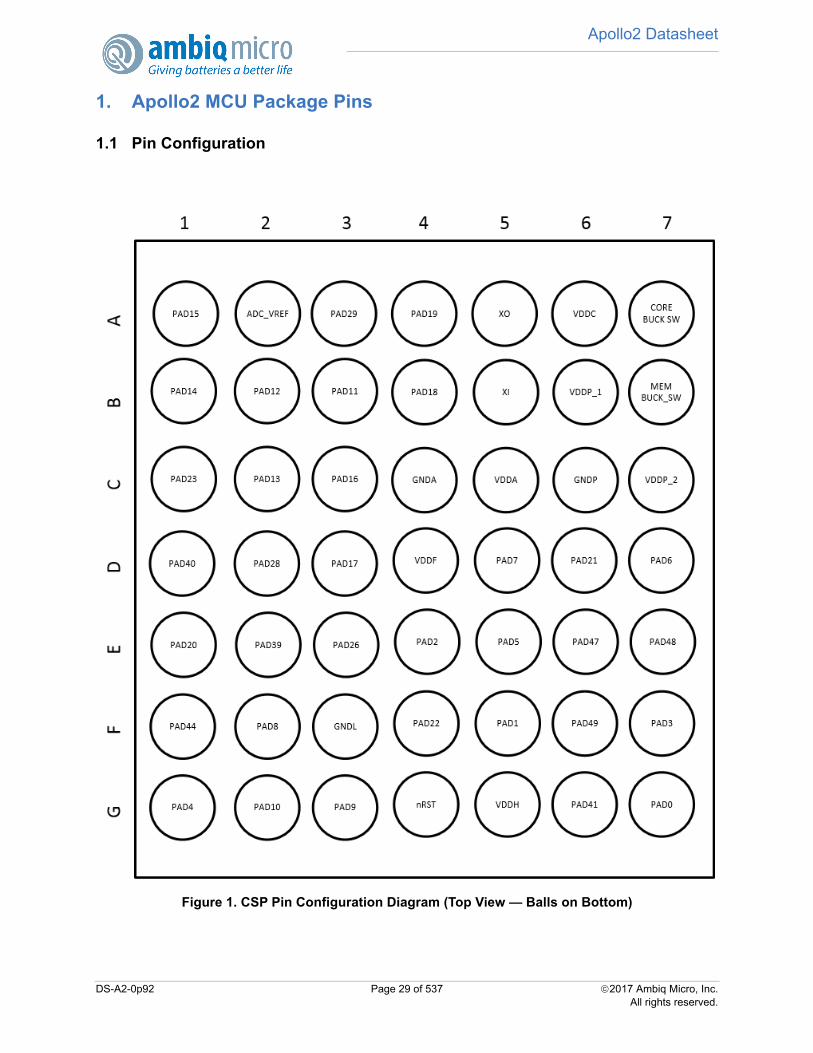
Apollo2 Datasheet
1. Apollo2 MCU Package Pins
1.1 Pin Configuration
Figure 1. CSP Pin Configuration Diagram (Top View — Balls on Bottom)
DS-A2-0p92 Page 29 of 537 2017 Ambiq Micro, Inc.All rights reserved.
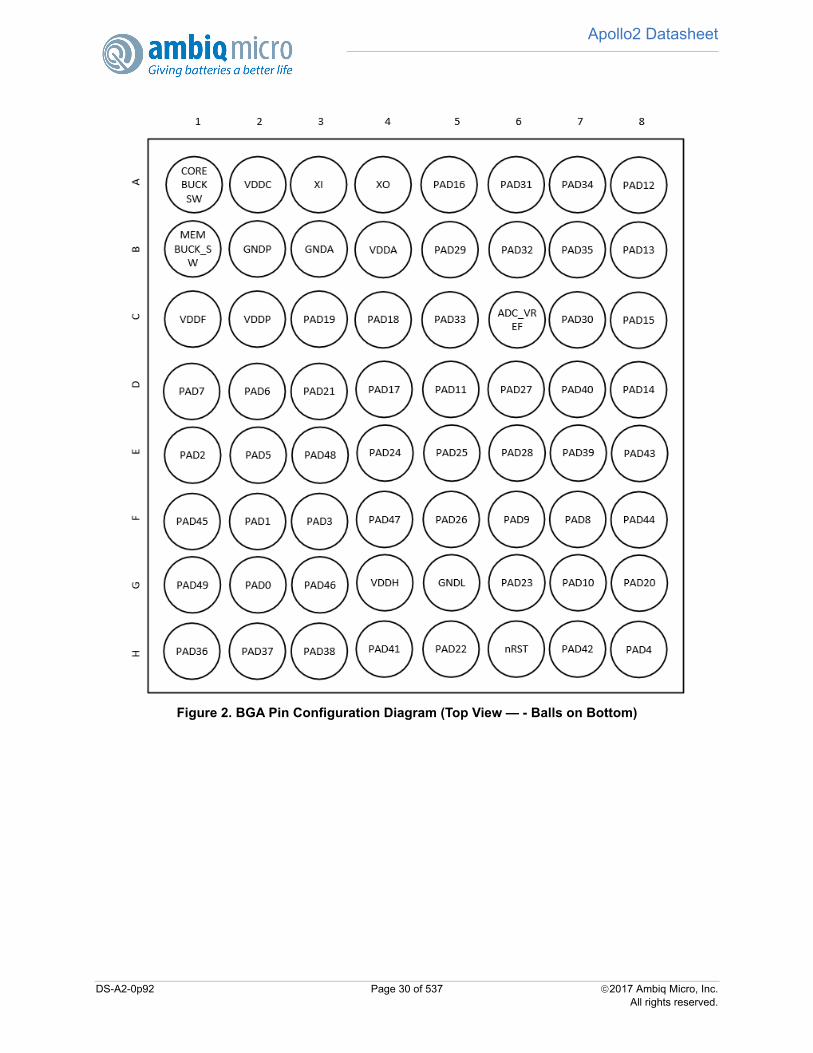
Apollo2 Datasheet
Figure 2. BGA Pin Configuration Diagram (Top View — - Balls on Bottom)
DS-A2-0p92 Page 30 of 537 2017 Ambiq Micro, Inc.All rights reserved.
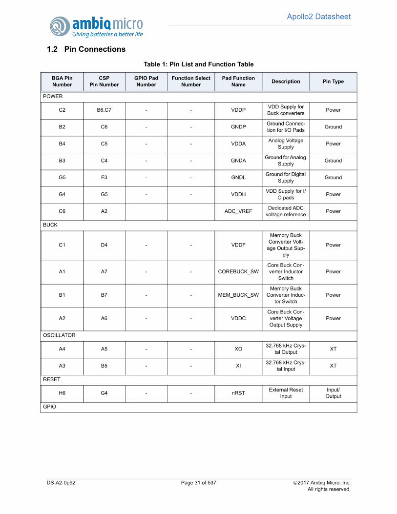
Apollo2 Datasheet
1.2 Pin Connections
Table 1: Pin List and Function Table
BGA Pin Number
CSP Pin Number
GPIO Pad Number
Function Select Number
Pad Function Name
Description Pin Type
POWER
C2 B6,C7 - - VDDPVDD Supply for Buck converters
Power
B2 C6 - - GNDPGround Connec-tion for I/O Pads
Ground
B4 C5 - - VDDAAnalog Voltage
SupplyPower
B3 C4 - - GNDAGround for Analog
SupplyGround
G5 F3 - - GNDLGround for Digital
SupplyGround
G4 G5 - - VDDHVDD Supply for I/
O padsPower
C6 A2 ADC_VREFDedicated ADC
voltage referencePower
BUCK
C1 D4 - - VDDF
Memory Buck Converter Volt-
age Output Sup-ply
Power
A1 A7 - - COREBUCK_SWCore Buck Con-verter Inductor
SwitchPower
B1 B7 - - MEM_BUCK_SWMemory Buck
Converter Induc-tor Switch
Power
A2 A6 - - VDDCCore Buck Con-verter Voltage Output Supply
Power
OSCILLATOR
A4 A5 - - XO32.768 kHz Crys-
tal OutputXT
A3 B5 - - XI32.768 kHz Crys-
tal InputXT
RESET
H6 G4 - - nRSTExternal Reset
InputInput/Output
GPIO
DS-A2-0p92 Page 31 of 537 2017 Ambiq Micro, Inc.All rights reserved.
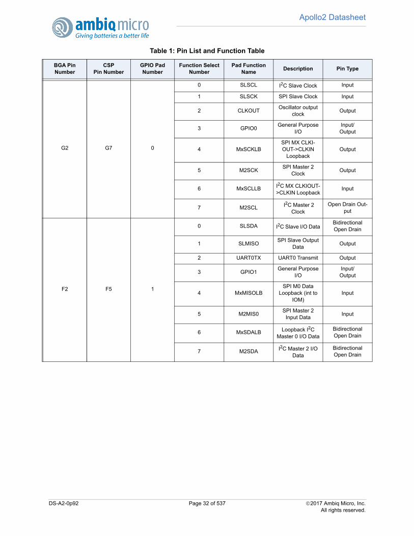
Apollo2 Datasheet
G2 G7 0
0 SLSCL I2C Slave Clock Input
1 SLSCK SPI Slave Clock Input
2 CLKOUTOscillator output
clockOutput
3 GPIO0General Purpose
I/OInput/Output
4 MxSCKLBSPI MX CLKI-OUT->CLKIN
LoopbackOutput
5 M2SCKSPI Master 2
ClockOutput
6 MxSCLLB I2C MX CLKIOUT->CLKIN Loopback
Input
7 M2SCL I2C Master 2 Clock
Open Drain Out-put
F2 F5 1
0 SLSDA I2C Slave I/O DataBidirectionalOpen Drain
1 SLMISOSPI Slave Output
DataOutput
2 UART0TX UART0 Transmit Output
3 GPIO1General Purpose
I/OInput/Output
4 MxMISOLBSPI M0 Data
Loopback (int to IOM)
Input
5 M2MIS0SPI Master 2
Input DataInput
6 MxSDALB Loopback I2C Master 0 I/O Data
BidirectionalOpen Drain
7 M2SDA I2C Master 2 I/O Data
BidirectionalOpen Drain
Table 1: Pin List and Function Table
BGA Pin Number
CSP Pin Number
GPIO Pad Number
Function Select Number
Pad Function Name
Description Pin Type
DS-A2-0p92 Page 32 of 537 2017 Ambiq Micro, Inc.All rights reserved.
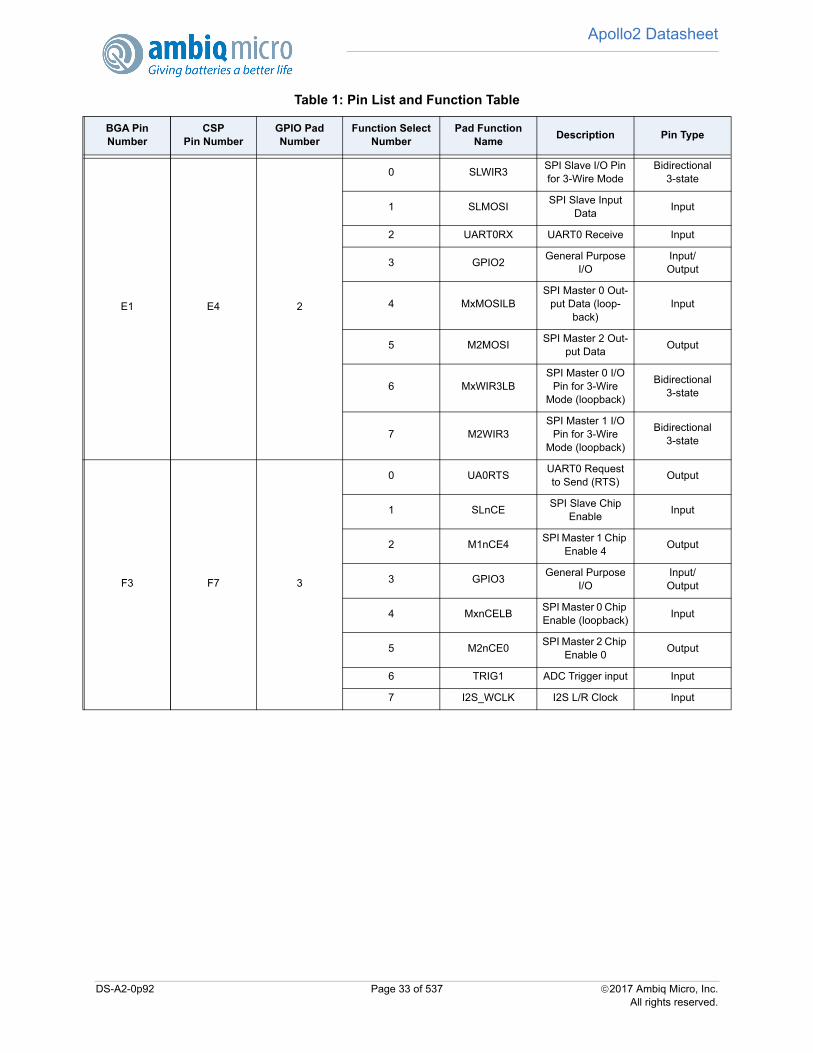
Apollo2 Datasheet
E1 E4 2
0 SLWIR3SPI Slave I/O Pin for 3-Wire Mode
Bidirectional3-state
1 SLMOSISPI Slave Input
DataInput
2 UART0RX UART0 Receive Input
3 GPIO2General Purpose
I/OInput/Output
4 MxMOSILBSPI Master 0 Out-
put Data (loop-back)
Input
5 M2MOSISPI Master 2 Out-
put DataOutput
6 MxWIR3LBSPI Master 0 I/O
Pin for 3-Wire Mode (loopback)
Bidirectional3-state
7 M2WIR3SPI Master 1 I/O
Pin for 3-Wire Mode (loopback)
Bidirectional3-state
F3 F7 3
0 UA0RTSUART0 Request to Send (RTS)
Output
1 SLnCESPI Slave Chip
EnableInput
2 M1nCE4SPI Master 1 Chip
Enable 4Output
3 GPIO3General Purpose
I/OInput/Output
4 MxnCELBSPI Master 0 Chip Enable (loopback)
Input
5 M2nCE0SPI Master 2 Chip
Enable 0Output
6 TRIG1 ADC Trigger input Input
7 I2S_WCLK I2S L/R Clock Input
Table 1: Pin List and Function Table
BGA Pin Number
CSP Pin Number
GPIO Pad Number
Function Select Number
Pad Function Name
Description Pin Type
DS-A2-0p92 Page 33 of 537 2017 Ambiq Micro, Inc.All rights reserved.

Apollo2 Datasheet
H8 G1 4
0 UA0CTSUART0 Clear to
Send (CTS)Input
1 SLINTConfigurable
Slave InterruptOutput
2 M0nCE5SPI Master 0 Chip
Enable 5Output
3 GPIO4General Purpose
I/OInput/Output
4 SLINTGPLoopback Slave
InterruptInput
5 M2nCE5SPI Master 2 Chip
Enable 5Output
6 CLKOUTOscillator Output
ClockOutput
7 32KHz_XT 32 kHz Clock Output
E2 E5 5
0 M0SCL I2C Master 0 Clock
Open Drain Out-put
1 M0SCKSPI Master 0
ClockOutput
2 UA0RTSUART0 Request To Send (RTS)
Output
3 GPIO5General Purpose
I/OInput/Output
4 M0SCKSPI Master 0
Clock (loopback)Output
5 RSVD AReserved for
future use
6 M0SCL I2C Master 0 Clock (loopback)
Open Drain Out-put
7 M1nCE2SPI Master 1 Chip
Enable 2Output
Table 1: Pin List and Function Table
BGA Pin Number
CSP Pin Number
GPIO Pad Number
Function Select Number
Pad Function Name
Description Pin Type
DS-A2-0p92 Page 34 of 537 2017 Ambiq Micro, Inc.All rights reserved.
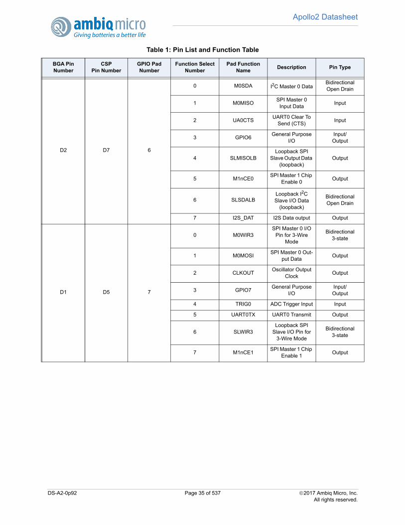
Apollo2 Datasheet
D2 D7 6
0 M0SDA I2C Master 0 DataBidirectionalOpen Drain
1 M0MISOSPI Master 0
Input DataInput
2 UA0CTSUART0 Clear To
Send (CTS)Input
3 GPIO6General Purpose
I/OInput/Output
4 SLMISOLBLoopback SPI
Slave Output Data (loopback)
Output
5 M1nCE0SPI Master 1 Chip
Enable 0Output
6 SLSDALBLoopback I2C Slave I/O Data
(loopback)
BidirectionalOpen Drain
7 I2S_DAT I2S Data output Output
D1 D5 7
0 M0WIR3SPI Master 0 I/O
Pin for 3-Wire Mode
Bidirectional3-state
1 M0MOSISPI Master 0 Out-
put DataOutput
2 CLKOUTOscillator Output
ClockOutput
3 GPIO7General Purpose
I/OInput/Output
4 TRIG0 ADC Trigger Input Input
5 UART0TX UART0 Transmit Output
6 SLWIR3Loopback SPI
Slave I/O Pin for 3-Wire Mode
Bidirectional3-state
7 M1nCE1SPI Master 1 Chip
Enable 1Output
Table 1: Pin List and Function Table
BGA Pin Number
CSP Pin Number
GPIO Pad Number
Function Select Number
Pad Function Name
Description Pin Type
DS-A2-0p92 Page 35 of 537 2017 Ambiq Micro, Inc.All rights reserved.

Apollo2 Datasheet
F7 F2 8
0 M1SCL I2C Master 1 Clock
Open Drain Out-put
1 M1SCKSPI Master 1
ClockOutput
2 M0nCE4SPI Master 0 Chip
Enable 4Output
3 GPIO8General Purpose
I/OInput/Output
4 M2nCE4SPI Master 2 Chip
Enable 4Output
5 M1SCKLBSPI Master 1
Clock (loopback)Output
6 UART1TX UART1 Transmit Output
7 M1SCLLB I2C Master 1 Clock (loopback)
Open Drain Out-put
F6 G3 9
0 M1SDA I2C Master 1 DataBidirectionalOpen Drain
1 M1MISOSPI Master 1
Input DataInput
2 M0nCE5SPI Master 0 Chip
Enable 5Output
3 GPIO9General Purpose
I/OInput/Output
4 M4nCE5SPI Master 4 Chip
Enable 5Output
5 SLMISOLBSPI Slave Output Data (loopback)
Output
6 UART1RX UART1 Receive Input
7 SLSDALB I2C Slave Data (loopback)
BidirectionalOpen Drain
Table 1: Pin List and Function Table
BGA Pin Number
CSP Pin Number
GPIO Pad Number
Function Select Number
Pad Function Name
Description Pin Type
DS-A2-0p92 Page 36 of 537 2017 Ambiq Micro, Inc.All rights reserved.
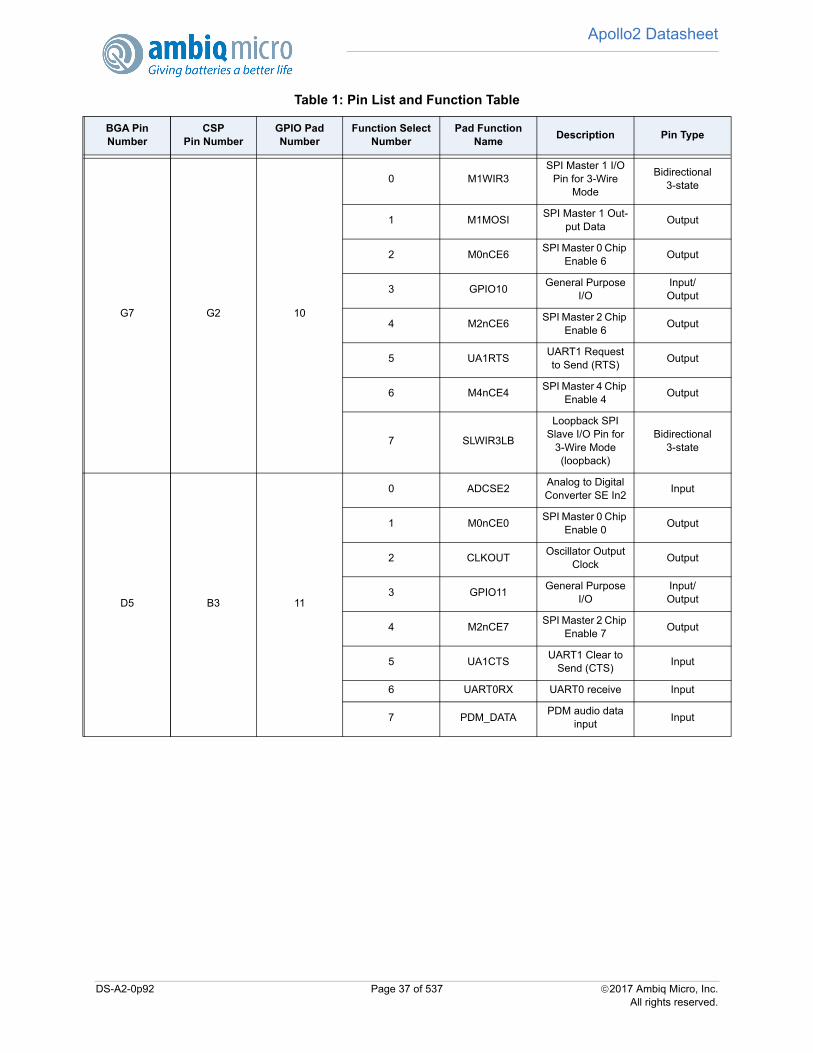
Apollo2 Datasheet
G7 G2 10
0 M1WIR3SPI Master 1 I/O
Pin for 3-Wire Mode
Bidirectional3-state
1 M1MOSISPI Master 1 Out-
put DataOutput
2 M0nCE6SPI Master 0 Chip
Enable 6Output
3 GPIO10General Purpose
I/OInput/Output
4 M2nCE6SPI Master 2 Chip
Enable 6Output
5 UA1RTSUART1 Request to Send (RTS)
Output
6 M4nCE4SPI Master 4 Chip
Enable 4Output
7 SLWIR3LB
Loopback SPI Slave I/O Pin for
3-Wire Mode (loopback)
Bidirectional3-state
D5 B3 11
0 ADCSE2Analog to Digital Converter SE In2
Input
1 M0nCE0SPI Master 0 Chip
Enable 0Output
2 CLKOUTOscillator Output
ClockOutput
3 GPIO11General Purpose
I/OInput/Output
4 M2nCE7SPI Master 2 Chip
Enable 7Output
5 UA1CTSUART1 Clear to
Send (CTS)Input
6 UART0RX UART0 receive Input
7 PDM_DATAPDM audio data
inputInput
Table 1: Pin List and Function Table
BGA Pin Number
CSP Pin Number
GPIO Pad Number
Function Select Number
Pad Function Name
Description Pin Type
DS-A2-0p92 Page 37 of 537 2017 Ambiq Micro, Inc.All rights reserved.
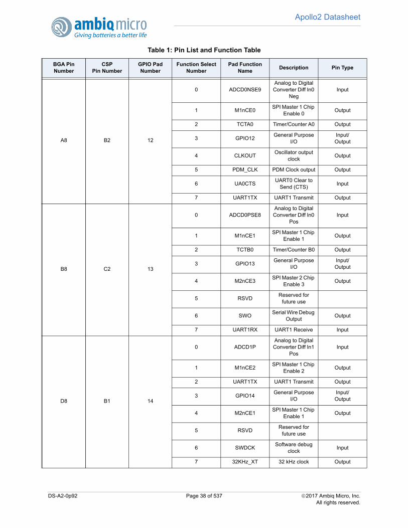
Apollo2 Datasheet
A8 B2 12
0 ADCD0NSE9Analog to Digital Converter Diff In0
NegInput
1 M1nCE0SPI Master 1 Chip
Enable 0Output
2 TCTA0 Timer/Counter A0 Output
3 GPIO12General Purpose
I/OInput/Output
4 CLKOUTOscillator output
clockOutput
5 PDM_CLK PDM Clock output Output
6 UA0CTSUART0 Clear to
Send (CTS)Input
7 UART1TX UART1 Transmit Output
B8 C2 13
0 ADCD0PSE8Analog to Digital Converter Diff In0
PosInput
1 M1nCE1SPI Master 1 Chip
Enable 1Output
2 TCTB0 Timer/Counter B0 Output
3 GPIO13General Purpose
I/OInput/Output
4 M2nCE3SPI Master 2 Chip
Enable 3Output
5 RSVDReserved for
future use
6 SWOSerial Wire Debug
OutputOutput
7 UART1RX UART1 Receive Input
D8 B1 14
0 ADCD1PAnalog to Digital Converter Diff In1
PosInput
1 M1nCE2SPI Master 1 Chip
Enable 2Output
2 UART1TX UART1 Transmit Output
3 GPIO14General Purpose
I/OInput/Output
4 M2nCE1SPI Master 1 Chip
Enable 1Output
5 RSVDReserved for
future use
6 SWDCKSoftware debug
clockInput
7 32KHz_XT 32 kHz clock Output
Table 1: Pin List and Function Table
BGA Pin Number
CSP Pin Number
GPIO Pad Number
Function Select Number
Pad Function Name
Description Pin Type
DS-A2-0p92 Page 38 of 537 2017 Ambiq Micro, Inc.All rights reserved.
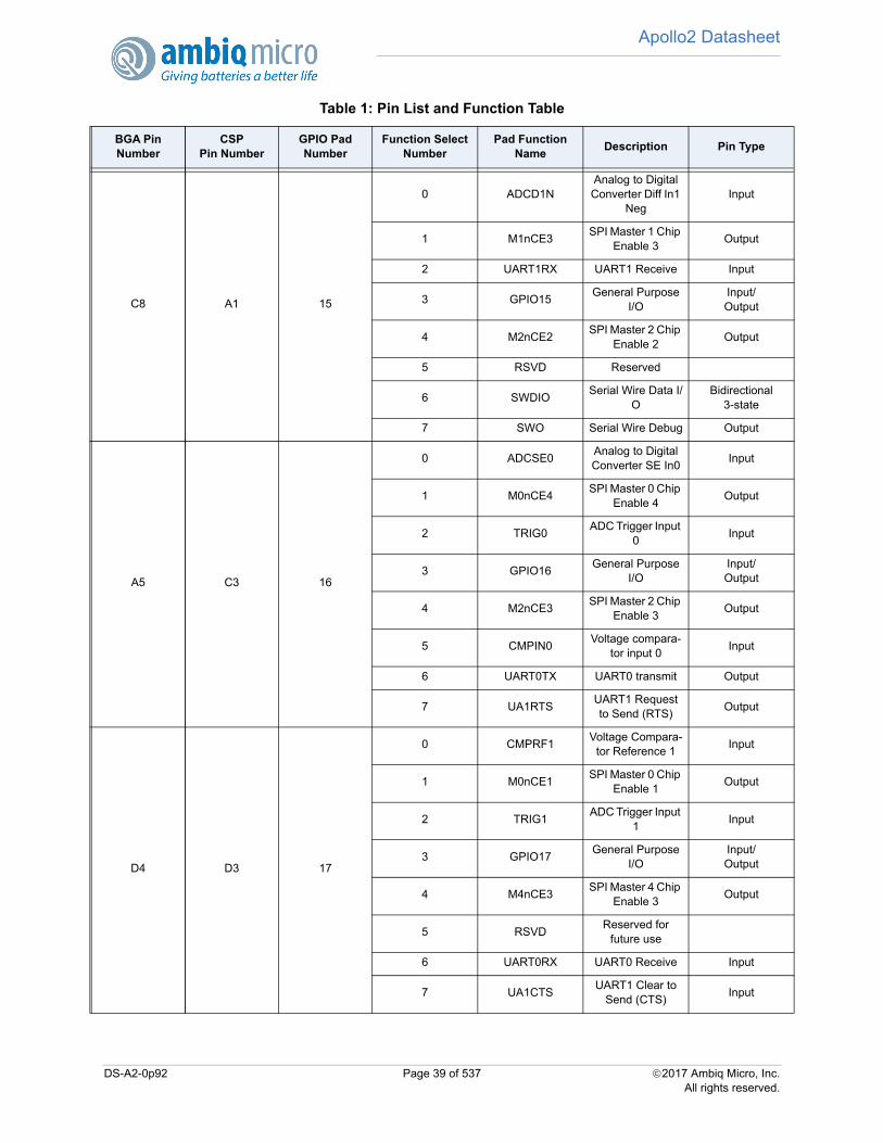
Apollo2 Datasheet
C8 A1 15
0 ADCD1NAnalog to Digital Converter Diff In1
NegInput
1 M1nCE3SPI Master 1 Chip
Enable 3Output
2 UART1RX UART1 Receive Input
3 GPIO15General Purpose
I/OInput/Output
4 M2nCE2SPI Master 2 Chip
Enable 2Output
5 RSVD Reserved
6 SWDIOSerial Wire Data I/
OBidirectional
3-state
7 SWO Serial Wire Debug Output
A5 C3 16
0 ADCSE0Analog to Digital Converter SE In0
Input
1 M0nCE4SPI Master 0 Chip
Enable 4Output
2 TRIG0ADC Trigger Input
0Input
3 GPIO16General Purpose
I/OInput/Output
4 M2nCE3SPI Master 2 Chip
Enable 3Output
5 CMPIN0Voltage compara-
tor input 0Input
6 UART0TX UART0 transmit Output
7 UA1RTSUART1 Request to Send (RTS)
Output
D4 D3 17
0 CMPRF1Voltage Compara-
tor Reference 1Input
1 M0nCE1SPI Master 0 Chip
Enable 1Output
2 TRIG1ADC Trigger Input
1Input
3 GPIO17General Purpose
I/OInput/Output
4 M4nCE3SPI Master 4 Chip
Enable 3Output
5 RSVD Reserved for
future use
6 UART0RX UART0 Receive Input
7 UA1CTSUART1 Clear to
Send (CTS)Input
Table 1: Pin List and Function Table
BGA Pin Number
CSP Pin Number
GPIO Pad Number
Function Select Number
Pad Function Name
Description Pin Type
DS-A2-0p92 Page 39 of 537 2017 Ambiq Micro, Inc.All rights reserved.
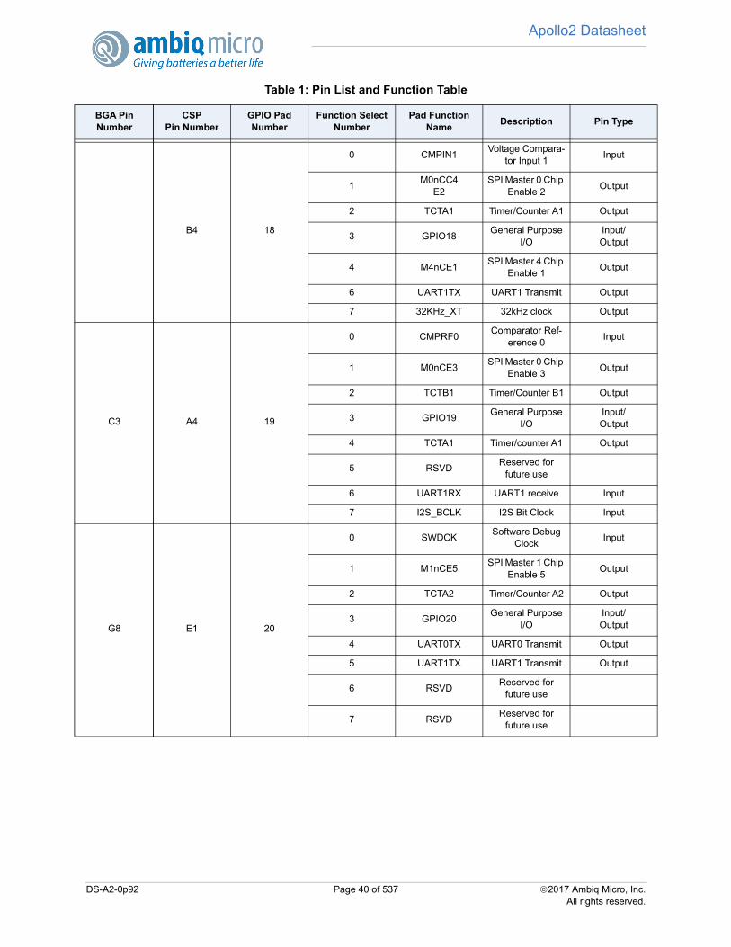
Apollo2 Datasheet
B4 18
0 CMPIN1Voltage Compara-
tor Input 1Input
1M0nCC4
E2SPI Master 0 Chip
Enable 2Output
2 TCTA1 Timer/Counter A1 Output
3 GPIO18General Purpose
I/OInput/Output
4 M4nCE1SPI Master 4 Chip
Enable 1Output
6 UART1TX UART1 Transmit Output
7 32KHz_XT 32kHz clock Output
C3 A4 19
0 CMPRF0Comparator Ref-
erence 0Input
1 M0nCE3SPI Master 0 Chip
Enable 3Output
2 TCTB1 Timer/Counter B1 Output
3 GPIO19General Purpose
I/OInput/Output
4 TCTA1 Timer/counter A1 Output
5 RSVDReserved for
future use
6 UART1RX UART1 receive Input
7 I2S_BCLK I2S Bit Clock Input
G8 E1 20
0 SWDCKSoftware Debug
ClockInput
1 M1nCE5SPI Master 1 Chip
Enable 5Output
2 TCTA2 Timer/Counter A2 Output
3 GPIO20General Purpose
I/OInput/Output
4 UART0TX UART0 Transmit Output
5 UART1TX UART1 Transmit Output
6 RSVDReserved for
future use
7 RSVDReserved for
future use
Table 1: Pin List and Function Table
BGA Pin Number
CSP Pin Number
GPIO Pad Number
Function Select Number
Pad Function Name
Description Pin Type
DS-A2-0p92 Page 40 of 537 2017 Ambiq Micro, Inc.All rights reserved.
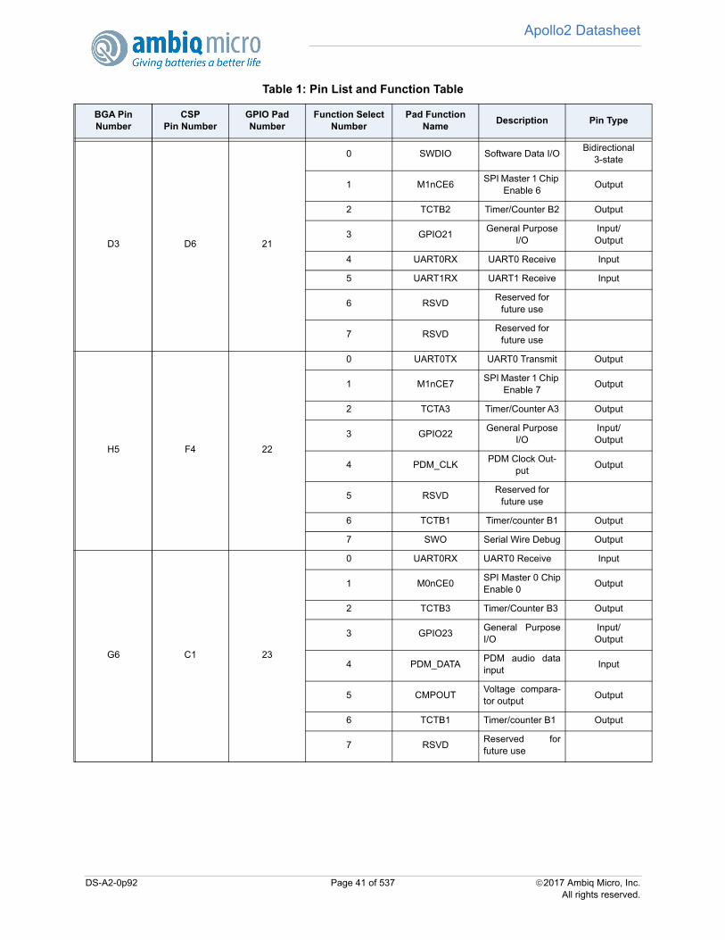
Apollo2 Datasheet
D3 D6 21
0 SWDIO Software Data I/OBidirectional
3-state
1 M1nCE6SPI Master 1 Chip
Enable 6Output
2 TCTB2 Timer/Counter B2 Output
3 GPIO21General Purpose
I/OInput/Output
4 UART0RX UART0 Receive Input
5 UART1RX UART1 Receive Input
6 RSVDReserved for
future use
7 RSVDReserved for
future use
H5 F4 22
0 UART0TX UART0 Transmit Output
1 M1nCE7SPI Master 1 Chip
Enable 7Output
2 TCTA3 Timer/Counter A3 Output
3 GPIO22General Purpose
I/OInput/Output
4 PDM_CLKPDM Clock Out-
putOutput
5 RSVDReserved for
future use
6 TCTB1 Timer/counter B1 Output
7 SWO Serial Wire Debug Output
G6 C1 23
0 UART0RX UART0 Receive Input
1 M0nCE0SPI Master 0 ChipEnable 0
Output
2 TCTB3 Timer/Counter B3 Output
3 GPIO23General PurposeI/O
Input/Output
4 PDM_DATAPDM audio datainput
Input
5 CMPOUTVoltage compara-tor output
Output
6 TCTB1 Timer/counter B1 Output
7 RSVDReserved forfuture use
Table 1: Pin List and Function Table
BGA Pin Number
CSP Pin Number
GPIO Pad Number
Function Select Number
Pad Function Name
Description Pin Type
DS-A2-0p92 Page 41 of 537 2017 Ambiq Micro, Inc.All rights reserved.
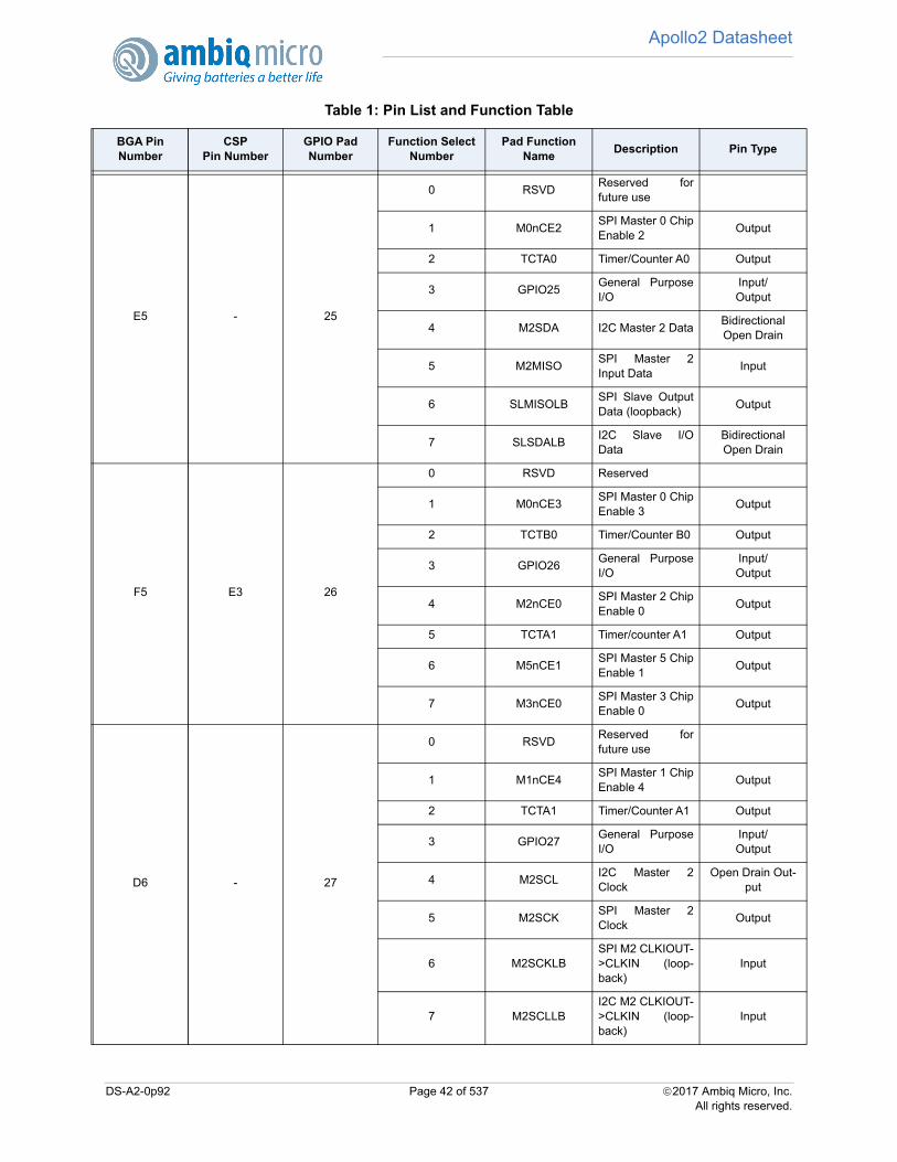
Apollo2 Datasheet
E5 - 25
0 RSVD Reserved forfuture use
1 M0nCE2SPI Master 0 ChipEnable 2
Output
2 TCTA0 Timer/Counter A0 Output
3 GPIO25General PurposeI/O
Input/Output
4 M2SDA I2C Master 2 DataBidirectional Open Drain
5 M2MISOSPI Master 2Input Data
Input
6 SLMISOLBSPI Slave OutputData (loopback)
Output
7 SLSDALBI2C Slave I/OData
Bidirectional Open Drain
F5 E3 26
0 RSVD Reserved
1 M0nCE3SPI Master 0 ChipEnable 3
Output
2 TCTB0 Timer/Counter B0 Output
3 GPIO26General PurposeI/O
Input/Output
4 M2nCE0SPI Master 2 ChipEnable 0
Output
5 TCTA1 Timer/counter A1 Output
6 M5nCE1SPI Master 5 ChipEnable 1
Output
7 M3nCE0SPI Master 3 ChipEnable 0
Output
D6 - 27
0 RSVD Reserved forfuture use
1 M1nCE4SPI Master 1 ChipEnable 4
Output
2 TCTA1 Timer/Counter A1 Output
3 GPIO27General PurposeI/O
Input/Output
4 M2SCLI2C Master 2Clock
Open Drain Out-put
5 M2SCKSPI Master 2Clock
Output
6 M2SCKLBSPI M2 CLKIOUT->CLKIN (loop-back)
Input
7 M2SCLLBI2C M2 CLKIOUT->CLKIN (loop-back)
Input
Table 1: Pin List and Function Table
BGA Pin Number
CSP Pin Number
GPIO Pad Number
Function Select Number
Pad Function Name
Description Pin Type
DS-A2-0p92 Page 42 of 537 2017 Ambiq Micro, Inc.All rights reserved.
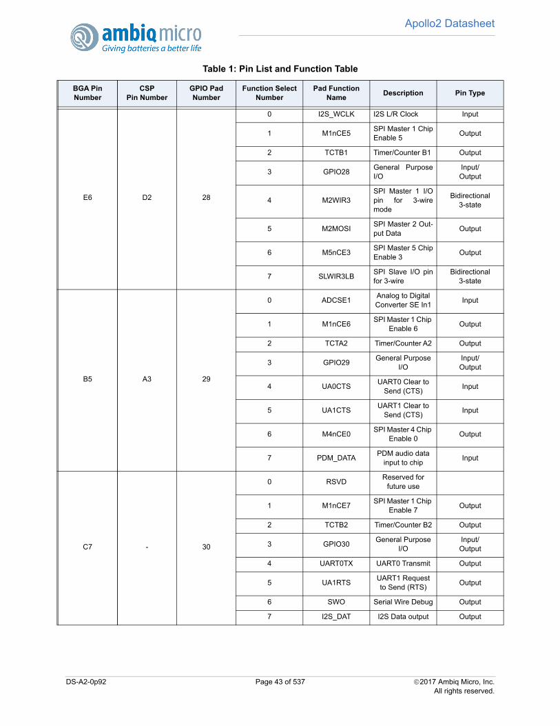
Apollo2 Datasheet
E6 D2 28
0 I2S_WCLK I2S L/R Clock Input
1 M1nCE5SPI Master 1 ChipEnable 5
Output
2 TCTB1 Timer/Counter B1 Output
3 GPIO28General PurposeI/O
Input/Output
4 M2WIR3SPI Master 1 I/Opin for 3-wiremode
Bidirectional 3-state
5 M2MOSISPI Master 2 Out-put Data
Output
6 M5nCE3SPI Master 5 ChipEnable 3
Output
7 SLWIR3LBSPI Slave I/O pinfor 3-wire
Bidirectional 3-state
B5 A3 29
0 ADCSE1Analog to Digital Converter SE In1
Input
1 M1nCE6SPI Master 1 Chip
Enable 6Output
2 TCTA2 Timer/Counter A2 Output
3 GPIO29General Purpose
I/OInput/ Output
4 UA0CTSUART0 Clear to
Send (CTS)Input
5 UA1CTSUART1 Clear to
Send (CTS)Input
6 M4nCE0SPI Master 4 Chip
Enable 0Output
7 PDM_DATAPDM audio data
input to chipInput
C7 - 30
0 RSVDReserved for
future use
1 M1nCE7SPI Master 1 Chip
Enable 7Output
2 TCTB2 Timer/Counter B2 Output
3 GPIO30General Purpose
I/OInput/Output
4 UART0TX UART0 Transmit Output
5 UA1RTSUART1 Request to Send (RTS)
Output
6 SWO Serial Wire Debug Output
7 I2S_DAT I2S Data output Output
Table 1: Pin List and Function Table
BGA Pin Number
CSP Pin Number
GPIO Pad Number
Function Select Number
Pad Function Name
Description Pin Type
DS-A2-0p92 Page 43 of 537 2017 Ambiq Micro, Inc.All rights reserved.

Apollo2 Datasheet
A6 - 31
0 ADCSE3Analog to DigitalConverter SE In3
Input
1 M0nCE4SPI Master 0 ChipEnable 4
Output
2 TCTA3 Timer/Counter A3 Output
3 GPIO31General PurposeI/O
Input/Output
4 UART0RX UART0 receive Input
5 TCTB1 Timer/counter B1 Output
6 RSVDReserved forfuture use
7 RSVDReserved forfuture use
B6 -- 32
0 ADCSE4Analog to DigitalConverter SEInput 4
Input
1 M0nCE5SPI Master 0 ChipEnable 5
Output
2 TCTB3 Timer/Counter B3 Output
3 GPIO32General PurposeI/O
Input/Output
4 RSVDReserved forfuture use
5 TCTB1 Timer/counter B1 Output
6 RSVDReserved forfuture use
7 RSVDReserved forfuture use
C5 - 33
0 ADCSE5Analog to DigitalConverter SE In5
Input
1 M0nCE6SPI Master 0 ChipEnable 6
Output
2 32KHz_XT 32kHz clock Output
3 GPIO33General PurposeI/O
Input/Output
4 RSVDReserved forfuture use
5 M3nCE7SPI Master 3 ChipEnable 7
Output
6 TCTB1 Timer/counter B1 Output
7 SWO Serial Wire Debug Output
Table 1: Pin List and Function Table
BGA Pin Number
CSP Pin Number
GPIO Pad Number
Function Select Number
Pad Function Name
Description Pin Type
DS-A2-0p92 Page 44 of 537 2017 Ambiq Micro, Inc.All rights reserved.

Apollo2 Datasheet
A7 - 34
0 ADCSE6Analog to DigitalConverter SE In6
Input
1 M0nCE7SPI Master 0 ChipEnable 7
Output
2 M2nCE3SPI Master 2 ChipEnable 3
Output
3 GPIO34General PurposeI/O
Input/Output
4 CMPRF2Comparator refer-ence 2
Input
5 M3nCE1SPI Master 3 ChipEnable 1
Output
6 M4nCE0SPI Master 4 ChipEnable 0
Output
7 M5nCE2SPI Master 5 ChipEnable 2
Output
B7 - 35
0 ADCSE7Analog to Digital Converter SE In7
Input
1 M1nCE0SPI Master 1 Chip
Enable 0Output
2 UART1TX UART1 Transmit Output
3 GPIO35General Purpose
I/OInput/Output
4 M4nCE6SPI Master 4 Chip
Enable 6Output
5 TCTA1 Timer/counter A1 Output
6 UA0RTSUART0 Request to Send (RTS)
Output
7 M3nCE2SPI Master 3 Chip
Enable 2Output
H1 - 36
0 TRIG1 ADC Trigger input Input
1 M1nCE1SPI Master 1 Chip
Enable 1Output
2 UART1RX UART1 Receive Input
3 GPIO36General Purpose
I/OInput/Output
4 32KHz_XT 32 kHz Clock Output
5 M2nCE0SPI Master 2 Chip
Enable 0Output
6 UA0CTSUART0 Clear to
Send (CTS)Input
7 M3nCE3SPI Master 3 Chip
Enable 3Output
Table 1: Pin List and Function Table
BGA Pin Number
CSP Pin Number
GPIO Pad Number
Function Select Number
Pad Function Name
Description Pin Type
DS-A2-0p92 Page 45 of 537 2017 Ambiq Micro, Inc.All rights reserved.
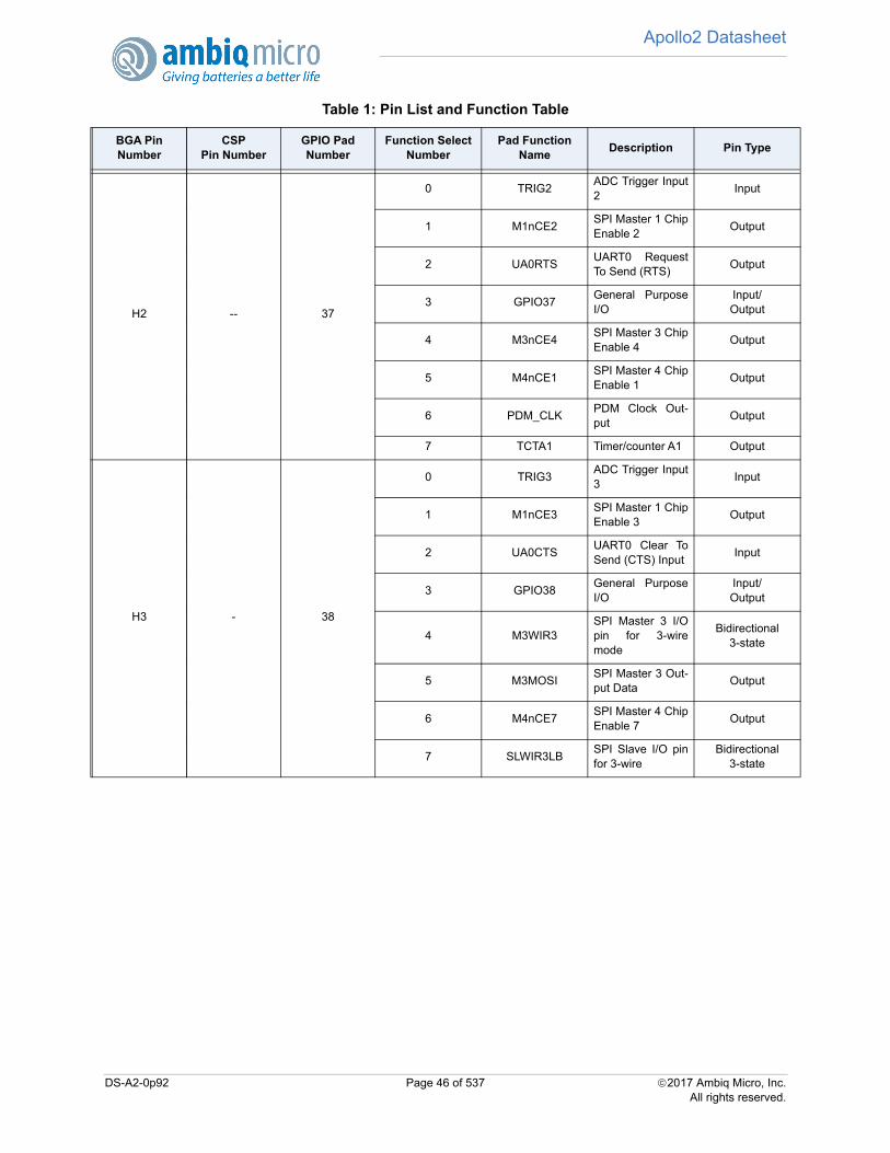
Apollo2 Datasheet
H2 -- 37
0 TRIG2ADC Trigger Input2
Input
1 M1nCE2SPI Master 1 ChipEnable 2
Output
2 UA0RTSUART0 RequestTo Send (RTS)
Output
3 GPIO37General PurposeI/O
Input/Output
4 M3nCE4SPI Master 3 ChipEnable 4
Output
5 M4nCE1SPI Master 4 ChipEnable 1
Output
6 PDM_CLKPDM Clock Out-put
Output
7 TCTA1 Timer/counter A1 Output
H3 - 38
0 TRIG3ADC Trigger Input3
Input
1 M1nCE3SPI Master 1 ChipEnable 3
Output
2 UA0CTSUART0 Clear ToSend (CTS) Input
Input
3 GPIO38General PurposeI/O
Input/Output
4 M3WIR3SPI Master 3 I/Opin for 3-wiremode
Bidirectional 3-state
5 M3MOSISPI Master 3 Out-put Data
Output
6 M4nCE7SPI Master 4 ChipEnable 7
Output
7 SLWIR3LBSPI Slave I/O pinfor 3-wire
Bidirectional 3-state
Table 1: Pin List and Function Table
BGA Pin Number
CSP Pin Number
GPIO Pad Number
Function Select Number
Pad Function Name
Description Pin Type
DS-A2-0p92 Page 46 of 537 2017 Ambiq Micro, Inc.All rights reserved.
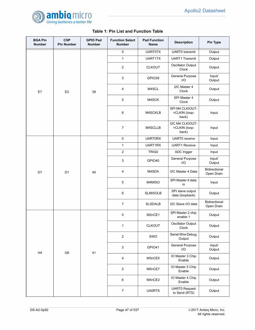
Apollo2 Datasheet
E7 E2 39
0 UART0TX UART0 transmit Output
1 UART1TX UART1 Transmit Output
2 CLKOUTOscillator Output
ClockOutput
3 GPIO39General Purpose
I/OInput/Output
4 M4SCLI2C Master 4
ClockOutput
5 M4SCKSPI Master 4
ClockOutput
6 M4SCKLBSPI M4 CLKIOUT-
>CLKIN (loop-back)
Input
7 M4SCLLBI2C M4 CLKIOUT-
>CLKIN (loop-back)
Input
D7 D1 40
0 UART0RX UART0 receive Input
1 UART1RX UART1 Receive Input
2 TRIG0 ADC trigger Input
3 GPIO40General Purpose
I/OInput/Output
4 M4SDA I2C Master 4 DataBidirectional Open Drain
5 M4MISOSPI Master 4 data
inInput
6 SLMISOLBSPI slave output data (loopback)
Output
7 SLSDALB I2C Slave I/O dataBidirectional Open Drain
H4 G6 41
0 M2nCE1SPI Master 2 chip
enable 1Output
1 CLKOUTOscillator Output
ClockOutput
2 SWOSerial Wire Debug
OutputOutput
3 GPIO41General Purpose
I/OInput/Output
4 M3nCE5IO Master 3 Chip
EnableOutput
5 M5nCE7IO Master 5 Chip
EnableOutput
6 M4nCE2IO Master 4 Chip
EnableOutput
7 UA0RTSUART0 Request to Send (RTS)
Output
Table 1: Pin List and Function Table
BGA Pin Number
CSP Pin Number
GPIO Pad Number
Function Select Number
Pad Function Name
Description Pin Type
DS-A2-0p92 Page 47 of 537 2017 Ambiq Micro, Inc.All rights reserved.
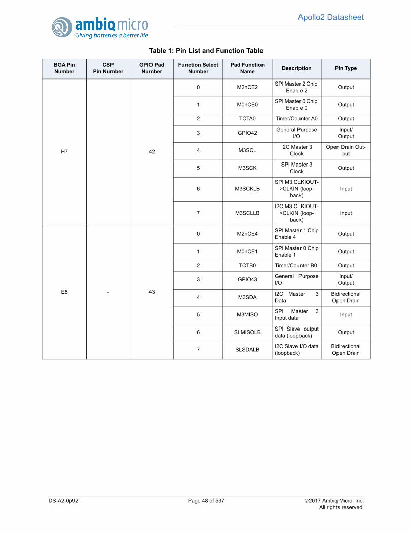
Apollo2 Datasheet
H7 - 42
0 M2nCE2SPI Master 2 Chip
Enable 2Output
1 M0nCE0SPI Master 0 Chip
Enable 0Output
2 TCTA0 Timer/Counter A0 Output
3 GPIO42General Purpose
I/OInput/Output
4 M3SCLI2C Master 3
ClockOpen Drain Out-
put
5 M3SCKSPI Master 3
ClockOutput
6 M3SCKLBSPI M3 CLKIOUT-
>CLKIN (loop-back)
Input
7 M3SCLLBI2C M3 CLKIOUT-
>CLKIN (loop-back)
Input
E8 - 43
0 M2nCE4SPI Master 1 ChipEnable 4
Output
1 M0nCE1SPI Master 0 ChipEnable 1
Output
2 TCTB0 Timer/Counter B0 Output
3 GPIO43General PurposeI/O
Input/Output
4 M3SDAI2C Master 3Data
Bidirectional Open Drain
5 M3MISOSPI Master 3Input data
Input
6 SLMISOLBSPI Slave outputdata (loopback)
Output
7 SLSDALBI2C Slave I/O data(loopback)
Bidirectional Open Drain
Table 1: Pin List and Function Table
BGA Pin Number
CSP Pin Number
GPIO Pad Number
Function Select Number
Pad Function Name
Description Pin Type
DS-A2-0p92 Page 48 of 537 2017 Ambiq Micro, Inc.All rights reserved.
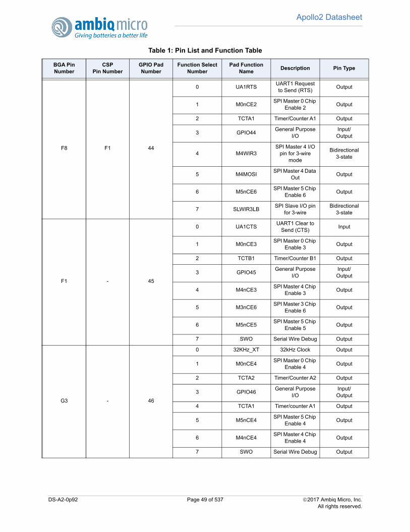
Apollo2 Datasheet
F8 F1 44
0 UA1RTSUART1 Request to Send (RTS)
Output
1 M0nCE2SPI Master 0 Chip
Enable 2Output
2 TCTA1 Timer/Counter A1 Output
3 GPIO44General Purpose
I/OInput/Output
4 M4WIR3SPI Master 4 I/O
pin for 3-wire mode
Bidirectional 3-state
5 M4MOSISPI Master 4 Data
OutOutput
6 M5nCE6SPI Master 5 Chip
Enable 6Output
7 SLWIR3LBSPI Slave I/O pin
for 3-wireBidirectional
3-state
F1 - 45
0 UA1CTSUART1 Clear to
Send (CTS)Input
1 M0nCE3SPI Master 0 Chip
Enable 3Output
2 TCTB1 Timer/Counter B1 Output
3 GPIO45General Purpose
I/OInput/Output
4 M4nCE3SPI Master 4 Chip
Enable 3Output
5 M3nCE6SPI Master 3 Chip
Enable 6Output
6 M5nCE5SPI Master 5 Chip
Enable 5Output
7 SWO Serial Wire Debug Output
G3 - 46
0 32KHz_XT 32kHz Clock Output
1 M0nCE4SPI Master 0 Chip
Enable 4Output
2 TCTA2 Timer/Counter A2 Output
3 GPIO46General Purpose
I/OInput/Output
4 TCTA1 Timer/counter A1 Output
5 M5nCE4SPI Master 5 Chip
Enable 4Output
6 M4nCE4SPI Master 4 Chip
Enable 4Output
7 SWO Serial Wire Debug Output
Table 1: Pin List and Function Table
BGA Pin Number
CSP Pin Number
GPIO Pad Number
Function Select Number
Pad Function Name
Description Pin Type
DS-A2-0p92 Page 49 of 537 2017 Ambiq Micro, Inc.All rights reserved.
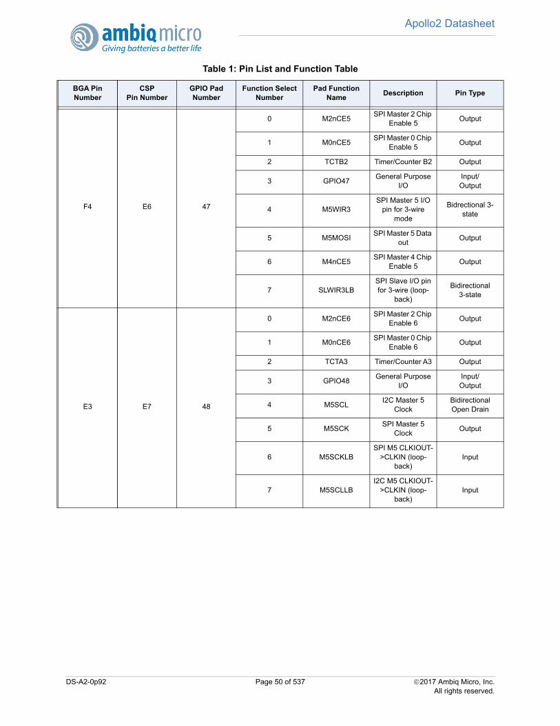
Apollo2 Datasheet
F4 E6 47
0 M2nCE5SPI Master 2 Chip
Enable 5Output
1 M0nCE5SPI Master 0 Chip
Enable 5Output
2 TCTB2 Timer/Counter B2 Output
3 GPIO47General Purpose
I/OInput/Output
4 M5WIR3SPI Master 5 I/O
pin for 3-wire mode
Bidrectional 3-state
5 M5MOSISPI Master 5 Data
outOutput
6 M4nCE5SPI Master 4 Chip
Enable 5Output
7 SLWIR3LBSPI Slave I/O pin for 3-wire (loop-
back)
Bidirectional 3-state
E3 E7 48
0 M2nCE6SPI Master 2 Chip
Enable 6Output
1 M0nCE6SPI Master 0 Chip
Enable 6Output
2 TCTA3 Timer/Counter A3 Output
3 GPIO48General Purpose
I/OInput/Output
4 M5SCLI2C Master 5
ClockBidirectional Open Drain
5 M5SCKSPI Master 5
ClockOutput
6 M5SCKLBSPI M5 CLKIOUT-
>CLKIN (loop-back)
Input
7 M5SCLLBI2C M5 CLKIOUT-
>CLKIN (loop-back)
Input
Table 1: Pin List and Function Table
BGA Pin Number
CSP Pin Number
GPIO Pad Number
Function Select Number
Pad Function Name
Description Pin Type
DS-A2-0p92 Page 50 of 537 2017 Ambiq Micro, Inc.All rights reserved.
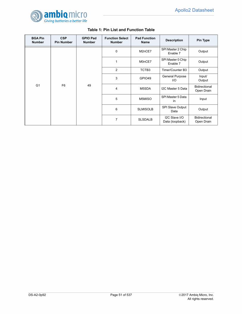
Apollo2 Datasheet
G1 F6 49
0 M2nCE7SPI Master 2 Chip
Enable 7Output
1 M0nCE7SPI Master 0 Chip
Enable 7Output
2 TCTB3 Timer/Counter B3 Output
3 GPIO49General Purpose
I/OInput/Output
4 M5SDA I2C Master 5 DataBidirectional Open Drain
5 M5MISOSPI Master 5 Data
inInput
6 SLMISOLBSPI Slave Output
DataOutput
7 SLSDALBI2C Slave I/O
Data (loopback)Bidirectional Open Drain
Table 1: Pin List and Function Table
BGA Pin Number
CSP Pin Number
GPIO Pad Number
Function Select Number
Pad Function Name
Description Pin Type
DS-A2-0p92 Page 51 of 537 2017 Ambiq Micro, Inc.All rights reserved.
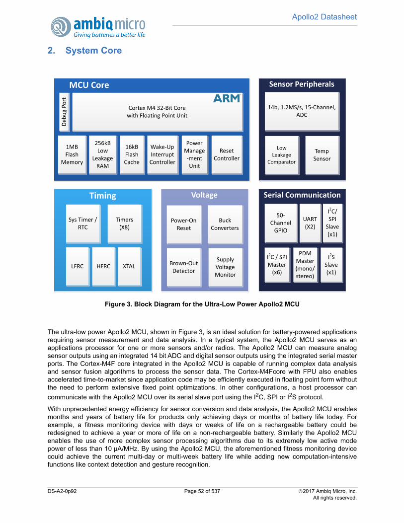
Apollo2 Datasheet
2. System Core
Figure 3. Block Diagram for the Ultra-Low Power Apollo2 MCU
The ultra-low power Apollo2 MCU, shown in Figure 3, is an ideal solution for battery-powered applicationsrequiring sensor measurement and data analysis. In a typical system, the Apollo2 MCU serves as anapplications processor for one or more sensors and/or radios. The Apollo2 MCU can measure analogsensor outputs using an integrated 14 bit ADC and digital sensor outputs using the integrated serial masterports. The Cortex-M4F core integrated in the Apollo2 MCU is capable of running complex data analysisand sensor fusion algorithms to process the sensor data. The Cortex-M4Fcore with FPU also enablesaccelerated time-to-market since application code may be efficiently executed in floating point form withoutthe need to perform extensive fixed point optimizations. In other configurations, a host processor can
communicate with the Apollo2 MCU over its serial slave port using the I2C, SPI or I2S protocol.
With unprecedented energy efficiency for sensor conversion and data analysis, the Apollo2 MCU enablesmonths and years of battery life for products only achieving days or months of battery life today. Forexample, a fitness monitoring device with days or weeks of life on a rechargeable battery could beredesigned to achieve a year or more of life on a non-rechargeable battery. Similarly the Apollo2 MCUenables the use of more complex sensor processing algorithms due to its extremely low active modepower of less than 10 µA/MHz. By using the Apollo2 MCU, the aforementioned fitness monitoring devicecould achieve the current multi-day or multi-week battery life while adding new computation-intensivefunctions like context detection and gesture recognition.
Cortex M4 32-Bit Core with Floating Point Unit
1MBFlash
Memory
256kBLow
LeakageRAM
Wake-Up Interrupt Controller
Power Manage-mentUnit
Reset Controller
Debu
g Po
rt
MCU Core
Timing Voltage
Sys Timer / RTC
Timers (X8)
LFRC HFRC XTAL Brown-Out Detector
Supply Voltage Monitor
Power-On Reset
Serial Communication
I2C / SPI Master
(x6)
I2C/SPI
Slave(x1)
Sensor Peripherals
Temp Sensor
Low Leakage
Comparator
UART(X2)
14b, 1.2MS/s, 15-Channel, ADC
Buck Converters
16kB Flash Cache
50-Channel
GPIO
PDM Master (mono/stereo)
I2S Slave (x1)
DS-A2-0p92 Page 52 of 537 2017 Ambiq Micro, Inc.All rights reserved.
Apollo2 Datasheet
At the center of the Apollo2 MCU is a 32-bit ARM Cortex-M4Fprocessor with Floating Point Unit withseveral tightly coupled peripherals. The Ambiq Micro implementation of the Cortex-M4Fcore delivers bothgreater performance and much lower power than 8-bit, 16-bit, and other comparable 32-bit cores. Codeand data may be stored in the 1 MB Flash Memory and the 256 KB Low Leakage RAM. The Wake-UpInterrupt Controller (WIC) coupled with the Cortex-M4Fsupports sophisticated and configurable sleep statetransitions with a variety of interrupt sources.
A rich set of sensor peripherals enable the monitoring of several sensors. An integrated temperaturesensor enables the measurement of ambient temperature. A scalable ultra-low power SuccessiveApproximation Register (SAR) Analog-to-Digital Converter (ADC) monitors the temperature sensor,several internal voltages, and up to eight external sensor signals. The ADC is uniquely tuned for minimumpower with a configurable measurement mode that does not require MCU intervention. In addition to
integrated analog sensor peripherals, I2C/SPI/PDM master ports and/or UART ports enables the MCU tocommunicate with external sensors and radios (such as Bluetooth transceivers) that have digital outputs.
The Apollo2 MCU also includes a set of timing peripherals and an RTC which is based on Ambiq’sAM08XX and AM18XX Real-Time Clock (RTC) families. The general purpose Timer/Counter Module(CTIMER), 32-bit System Timer (STIMER), and the RTC may be driven independently by one of threedifferent clock sources: a low frequency RC oscillator, a high frequency RC oscillator, and a 32.768 kHzcrystal (XTAL) oscillator. These clock sources use the proprietary advanced calibration techniquesdeveloped for the AM08XX and AM18XX products that achieve XTAL-like accuracy with RC-like power.Additionally, the Apollo2 MCU includes clock reliability functions first offered in the AM08XX and AM18XXproducts. For example, the RTC can automatically switch from an XTAL source to an RC source in theevent of an XTAL failure.
As with any ARM-based MCU, the Apollo2 MCU is supported by a complete suite of standard softwaredevelopment tools. Ambiq Micro provides drivers for all peripherals along with basic application code toshorten development times. Software debug is facilitated by the addition of an Instrumentation TraceMacrocell (ITM), a Trace Port Interface Unit (TPIU) and through the use of a Serial Wire Debuggerinterface (SWD).
DS-A2-0p92 Page 53 of 537 2017 Ambiq Micro, Inc.All rights reserved.
Apollo2 Datasheet
3. MCU Core Details
At the center of the Apollo2 MCU is a 32-bit ARM Cortex-M4F core with the floating point option. This 3-stage pipeline implementation of the ARM v7-M architecture offers highly efficient processing in a very lowpower design. The ARM M DAP enables debugging access via a Serial Wire Interface from outside of theMCU which allows access to all of the memory and peripheral devices of the MCU. The M4F core offerssome other advantages including:
Single 4 GB memory architecture with all Peripherals being memory-mapped Low-Power Consumption Modes:
- Active- Sleep- Deep-Sleep- Power-Off
Interrupts and Events- NVIC – interrupt controller- WIC – Wake-Up Interrupt Controller- Sleep-on-Exit (reduces interrupt overhead, used in an ISR SW structure)- WFI (enter sleep modes, wait for interrupts)
The following sections provide behavioral and performance details about each of the peripherals controlled
by the MCU core. Where multiple instances of a peripheral exist on Apollo2 MCU (e.g., the six I2C/SPImaster modules), base memory addresses for the registers are provided for each and noted asINSTANCE 0, INSTANCE 1, etc.
3.1 InterruptsWithin the MCU, multiple peripherals can generate interrupts. In some cases, a single peripheral may beable to generate multiple different interrupts. Each interrupt signal generated by a peripheral is connectedback to the M4F core in two places. First, the interrupts are connected to the Nested Vectored InterruptController, NVIC, in the core. This connection provides the standard changes to program flow associatedwith interrupt processing. Additionally, they are connected to the WIC outside of the core, allowing theinterrupt sources to wake the M4F core when it is in a deep sleep (SRPG) mode.
The MCU supports the M4F NMI as well as the normal interrupt types. For details on the Interrupt model ofthe M4F, please see the “Cortex-M4F Devices Generic User Guide,” document number DUI0553A.
Below is the M4F Vector Table:
DS-A2-0p92 Page 54 of 537 2017 Ambiq Micro, Inc.All rights reserved.
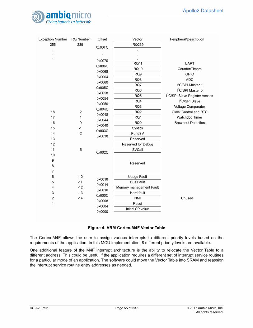
Apollo2 Datasheet
Figure 4. ARM Cortex-M4F Vector Table
The Cortex-M4F allows the user to assign various interrupts to different priority levels based on therequirements of the application. In this MCU implementation, 8 different priority levels are available.
One additional feature of the M4F interrupt architecture is the ability to relocate the Vector Table to adifferent address. This could be useful if the application requires a different set of interrupt service routinesfor a particular mode of an application. The software could move the Vector Table into SRAM and reassignthe interrupt service routine entry addresses as needed.
Exception Number IRQ Number Offset255 239
0x03FC...
.
.
.
0x004C18 2
0x004817 1
0x004416 0
0x004015 -1
0x003C14 -2
0x0038131211 -5
0x002C109876 -10
0x00185 -11
0x00144 -12
0x00103 -13
0x000C2 -14
0x00081
0x00040x0000
VectorIRQ239
.
.
.
IRQ2IRQ1IRQ0
SystickPendSV
ReservedReserved for Debug
SVCall
Reserved
Usage FaultBus Fault
Memory management FaultHard fault
NMIReset
Initial SP value
IRQ3IRQ4IRQ5IRQ6IRQ7IRQ8IRQ9
IRQ10IRQ11
Peripheral/Description
0x00500x00540x00580x005C0x00600x00640x00680x006C0x0070
Unused
Brownout DetectionWatchdog Timer
Clock Control and RTCVoltage Comparator
I2C/SPI SlaveI2C/SPI Slave Register Access
I2C/SPI Master 0I2C/SPI Master 1
ADCGPIO
Counter/TimersUART
DS-A2-0p92 Page 55 of 537 2017 Ambiq Micro, Inc.All rights reserved.
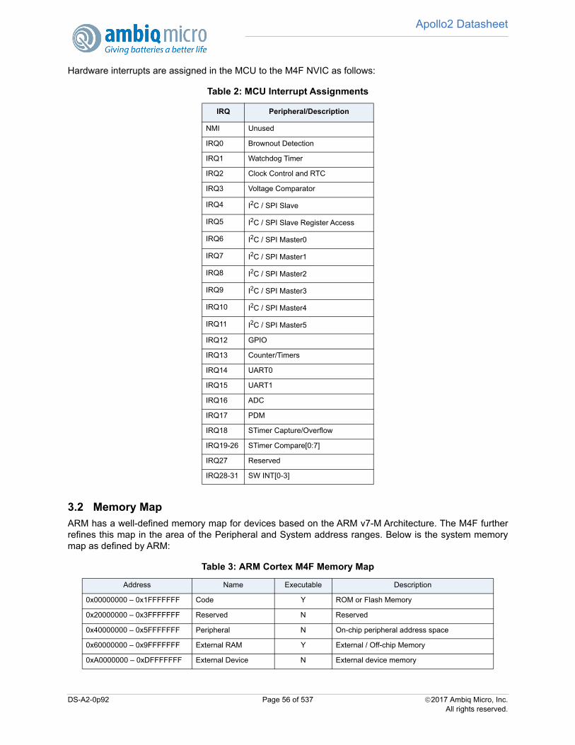
Apollo2 Datasheet
Hardware interrupts are assigned in the MCU to the M4F NVIC as follows:
3.2 Memory MapARM has a well-defined memory map for devices based on the ARM v7-M Architecture. The M4F furtherrefines this map in the area of the Peripheral and System address ranges. Below is the system memorymap as defined by ARM:
Table 2: MCU Interrupt Assignments
IRQ Peripheral/Description
NMI Unused
IRQ0 Brownout Detection
IRQ1 Watchdog Timer
IRQ2 Clock Control and RTC
IRQ3 Voltage Comparator
IRQ4 I2C / SPI Slave
IRQ5 I2C / SPI Slave Register Access
IRQ6 I2C / SPI Master0
IRQ7 I2C / SPI Master1
IRQ8 I2C / SPI Master2
IRQ9 I2C / SPI Master3
IRQ10 I2C / SPI Master4
IRQ11 I2C / SPI Master5
IRQ12 GPIO
IRQ13 Counter/Timers
IRQ14 UART0
IRQ15 UART1
IRQ16 ADC
IRQ17 PDM
IRQ18 STimer Capture/Overflow
IRQ19-26 STimer Compare[0:7]
IRQ27 Reserved
IRQ28-31 SW INT[0-3]
Table 3: ARM Cortex M4F Memory Map
Address Name Executable Description
0x00000000 – 0x1FFFFFFF Code Y ROM or Flash Memory
0x20000000 – 0x3FFFFFFF Reserved N Reserved
0x40000000 – 0x5FFFFFFF Peripheral N On-chip peripheral address space
0x60000000 – 0x9FFFFFFF External RAM Y External / Off-chip Memory
0xA0000000 – 0xDFFFFFFF External Device N External device memory
DS-A2-0p92 Page 56 of 537 2017 Ambiq Micro, Inc.All rights reserved.

Apollo2 Datasheet
The MCU-specific implementation of this memory map is as follows:
Peripheral devices within the memory map are allocated on 4 KB boundaries, allowing each device up to1024 32-bit control and status registers. Peripherals will return undefined read data when an attempt toaccess a register which does not exist occurs. Peripherals, whether accessed via the APB or the AHB, willalways accept any write data sent to their registers without attempting to return an ERROR response.Specifically, a write to a read-only register would just become a don’t-care write.
0xE0000000 – 0xE00FFFFF Private Peripheral Bus N NVIC, System timers, System Control Block
0xE0100000 – 0xFFFFFFFF Vendor N Vendor Defined
Table 4: MCU System Memory Map
Address Name Executable Description
0x00000000 – 0x000FFFFF Flash Y Flash Memory
0x00100000 – 0x07FFFFFF Reserved X No device at this address range
0x08000000 – 0x08000FFF Boot Loader ROM YExecute Only Boot Loader and Flash HelperFunctions.
0x08001000 – 0x0FFFFFFF Reserved X No device at this address range
0x10000000 – 0x1003FFFF SRAM Y Low-power SRAM
0x10040000 – 0x3FFFFFFF Reserved X No device at this address range
0x40000000 – 0x4FFFFFFF Peripheral – APB N APB Peripheral devices
0x50000000 – 0x5FFFFFFF Peripheral – AHB N AHB Peripheral devices
0x60000000 – 0xDFFFFFFF Reserved X No device at this address range
0xE0000000 – 0xE00FFFFF PPB N NVIC, System timers, System Control Block
0xE0100000 – 0xEFFFFFFF Reserved X No device at this address range
0xF0000000 – 0xF0000FFF Reserved X No device at this address range
0xF0001000 – 0xFFFFFFFF Reserved X No device at this address range
Table 3: ARM Cortex M4F Memory Map
Address Name Executable Description
DS-A2-0p92 Page 57 of 537 2017 Ambiq Micro, Inc.All rights reserved.
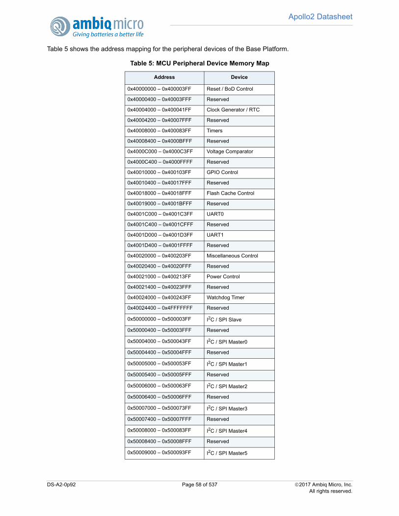
Apollo2 Datasheet
Table 5 shows the address mapping for the peripheral devices of the Base Platform.
Table 5: MCU Peripheral Device Memory Map
Address Device
0x40000000 – 0x400003FF Reset / BoD Control
0x40000400 – 0x40003FFF Reserved
0x40004000 – 0x400041FF Clock Generator / RTC
0x40004200 – 0x40007FFF Reserved
0x40008000 – 0x400083FF Timers
0x40008400 – 0x4000BFFF Reserved
0x4000C000 – 0x4000C3FF Voltage Comparator
0x4000C400 – 0x4000FFFF Reserved
0x40010000 – 0x400103FF GPIO Control
0x40010400 – 0x40017FFF Reserved
0x40018000 – 0x40018FFF Flash Cache Control
0x40019000 – 0x4001BFFF Reserved
0x4001C000 – 0x4001C3FF UART0
0x4001C400 – 0x4001CFFF Reserved
0x4001D000 – 0x4001D3FF UART1
0x4001D400 – 0x4001FFFF Reserved
0x40020000 – 0x400203FF Miscellaneous Control
0x40020400 – 0x40020FFF Reserved
0x40021000 – 0x400213FF Power Control
0x40021400 – 0x40023FFF Reserved
0x40024000 – 0x400243FF Watchdog Timer
0x40024400 – 0x4FFFFFFF Reserved
0x50000000 – 0x500003FF I2C / SPI Slave
0x50000400 – 0x50003FFF Reserved
0x50004000 – 0x500043FF I2C / SPI Master0
0x50004400 – 0x50004FFF Reserved
0x50005000 – 0x500053FF I2C / SPI Master1
0x50005400 – 0x50005FFF Reserved
0x50006000 – 0x500063FF I2C / SPI Master2
0x50006400 – 0x50006FFF Reserved
0x50007000 – 0x500073FF I2C / SPI Master3
0x50007400 – 0x50007FFF Reserved
0x50008000 – 0x500083FF I2C / SPI Master4
0x50008400 – 0x50008FFF Reserved
0x50009000 – 0x500093FF I2C / SPI Master5
DS-A2-0p92 Page 58 of 537 2017 Ambiq Micro, Inc.All rights reserved.

Apollo2 Datasheet
3.3 Memory Protection Unit (MPU)The Apollo2 MCU includes an MPU which is a core component for memory protection. The M4F processorsupports the standard ARMv7 Protected Memory System Architecture model. The MPU provides fullsupport for:
Protection regions. Overlapping protection regions, with ascending region priority:
- 7 = highest priority- 0 = lowest priority.
Access permissions Exporting memory attributes to the system.
MPU mismatches and permission violations invoke the programmable-priority MemManage fault handler.
See the ARM®v7-M Architecture Reference Manual for more information.
You can use the MPU to:
Enforce privilege rules. Separate processes. Enforce access rules.
3.4 System BussesThe ARM Cortex-M4F utilizes 3 instances of the AMBA AHB bus for communication with memory andperipherals. The ICode bus is designed for instruction fetches from the ‘Code’ memory space while theDCode bus is designed for data and debug accesses in that same region. The System bus is designed forfetches to the SRAM and other peripheral devices of the MCU.
The Apollo2 MCU maps the available SRAM memory onto an address space within the ‘Code’ memoryspace. This gives the user the opportunity to perform instruction and data fetches from the lower-powerSRAM to effectively lower the power consumption of the MCU.
The peripherals of the Apollo2 MCU which are infrequently accessed are located on an AMBA APB bus. Abridge exists which translates the accesses from the System AHB to the APB. Accesses to theseperipherals will inject a single wait-state on the AHB during any access cycle.
3.5 Power ManagementThe Power Management Unit (PMU) is a finite-state machine that controls the transitions of the MCUbetween power modes. When moving from Active Mode to Deep Sleep Mode, the PMU manages thestate-retention capability of the registers within the Cortex M4F core and also controls the shutdown of thevoltage regulators of the MCU. Once in the Deep Sleep Mode, the PMU, in conjunction with the Wake-Up
0x50009400 – 0x5000FFFF Reserved
0x50010000 – 0x500103FF ADC
0x50010400 – 0x50010FFF Reserved
0x50011000 – 0x500113FF PDM
0x50011400 – 0x5001FFFF Reserved
0x50020000 – 0x5002FFFF Flash OTP
0x50030000 – 0x5FFFFFFF Reserved
Table 5: MCU Peripheral Device Memory Map
Address Device
DS-A2-0p92 Page 59 of 537 2017 Ambiq Micro, Inc.All rights reserved.

Apollo2 Datasheet
Interrupt Controller, waits for a wakeup event. When the event is observed, the PMU begins the powerrestoration process by re-enabling the on-chip voltage regulators and restoring the CPU register state. TheM4F is then returned to active mode once all state is ready.
The Apollo2 MCU power modes are described in the subsequent discussion along with the operation ofthe PMU.
3.5.1 Cortex M4 Power Modes
The ARM Cortex M4 defines the following 3 power modes:
Active Sleep Deep Sleep
In addition to the above ARM-defined modes, the Apollo2 MCU will support a Shutdown mode in which theentire device is powered down except for the logic required to support a Power-On Reset.
Each mode is described below.
3.5.1.1 Active Mode
In the Active Mode, the M4 is powered up, clocks are active, and instructions are being executed. In thismode, the M4 expects all (enabled) devices attached to the AHB and APB to be powered and clocked fornormal access. All of the non-debug ARM clocks (FCLK, HCLK) are active in this state.
To transition from the Active Mode to any of the lower-power modes, a specific sequence of instructions isexecuted on the M4 core. First, specific bits in the ARMv7-M System Control Register must be set todetermine the mode to enter. See page B3-269 of the ARMv7-M Architecture Reference Manual for moredetails.
After the SCR is setup, code can enter the low-power states using one of the 2 following methods:
Execute a Wait-For-Interrupt (WFI) instruction Set the SLEEPONEXIT bit of the SCR such that the exit from an ISR will automatically return to a sleep
state.
The M4 will enter a low-power mode after one of these are performed (assuming all conditions are met)and remain there until some event causes the core to return to Active Mode. The possible reasons toreturn to Active Mode are:
A reset An enabled Interrupt is received by the NVIC A Debug Event is received from the DAP
3.5.1.2 Sleep Mode
In the Sleep Mode, the M4 is powered up, but the clocks (HCLK, FCLK) are not active. The power supplyis still applied to the M4 logic such that it can immediately become active on a wakeup event and beginexecuting instructions.
3.5.1.3 Deep Sleep Mode
In the Deep Sleep Mode, the M4 enters SRPG mode where the main power is removed, but the flopsretain their state. The clocks are not active, and the MCU clock sources for HCLK and FCLK can bedeactivated. To facilitate the removal of the source supply and entry into SRPG mode, the M4 willhandshake with the Wake-up Interrupt Controller and Power Management Unit and set up the possiblewakeup conditions.
DS-A2-0p92 Page 60 of 537 2017 Ambiq Micro, Inc.All rights reserved.
Apollo2 Datasheet
3.5.2 System Power Modes
In addition to the CPU power states, there are system power states defined as follows.
3.5.2.1 SYS Active (SACT)
CPU is in Active Mode and executing instructions. All peripheral devices are on and available.
3.5.2.2 SYS Sleep Mode 0 (SS0)
In SYS Sleep Mode 0, this is a low power state for the MCU. In this mode, all SRAM memory is retained(256KB), Flash memory is in standby, HFRC is on, main core clock domain is gated but peripheral clockdomains can be on. CPU is in Sleep Mode.
This state can be entered if a peripheral device (SPI/UART/I2C) is actively transferring data and the timewindow is sufficient for CPU to enter Sleep Mode but is not long enough to go into a Deep Sleep Mode.
3.5.2.3 SYS Sleep Mode 1 (SS1)
In SYS Sleep Mode 1, this is a low power state for the MCU. In this mode, all SRAM memory is retained(256 KB), Flash memory is in standby, HFRC is on, all functional clocks are gated. CPU is in Sleep Mode.
This state can be entered if a no peripheral device (SPI/UART/I2C) is actively transferring data, however,communication may occur within a short time window which will prevent the CPU from entering DeepSleep Mode (and subsequently the system from entering a lower power state).
This state is also referred to as “Active Idle”. In other words, all power domains are powered on, but allclocks are gated. This state is a good power baseline for the system as it represents the active mode DCpower level. Typically the power in this state is dominated by leakage, always-on functional blocks andpotentially other blocks that are not efficiently clock gated.
3.5.2.4 SYS Deep Sleep Mode 0 (SDS0)
In SYS Deep Sleep Mode 0, this is a deep low power state for the MCU. In this mode, SRAM is in retention(capacity controlled by software), cache memory is in retention (16 KB), Flash memory is in power down,HFRC is on, main core power domain is off but peripheral power domains can be on. CPU is in DeepSleep. Core logic state is retained.
This state can be entered if a peripheral device (SPI/UART/I2C) is actively (or intermittently) transferringdata but the window of acquisition is long enough to allow the CPU to go into a deeper low power state.
Note: For easier notation, SRAM memory retention is defined as follows:
256KB: SDS0-256RET
128KB: SDS0-128RET
64KB: SDS0-64RET
8KB: SDS0-8RET
0KB: SDS0
3.5.2.5 SYS Deep Sleep Mode 1 (SDS1)
In SYS Deep Sleep Mode 1, this is a deep low power state for the MCU. In this mode, SRAM is in retention(capacity controlled by software), cache memory is powered down, Flash memory is in power down, HFRCis on, main core power domain is off but peripheral power domains can be on. CPU is in Deep Sleep. Corelogic state is retained.
DS-A2-0p92 Page 61 of 537 2017 Ambiq Micro, Inc.All rights reserved.

Apollo2 Datasheet
This state can be entered if the latency to warm up the cache can be tolerated. This could be an extendedwait for peripheral communication event.
Note: For easier notation, SRAM memory retention is defined as follows:
256KB: SDS1-256RET
128KB: SDS1-128RET
64KB: SDS1-64RET
8KB: SDS1-8RET
0KB: SDS1
3.5.2.6 SYS Deep Sleep Mode 2 (SDS2)
In SYS Deep Sleep Mode 2, this is the minimum power state that the MCU can resume normal operation.In this mode, minimal SRAM memory is retained as needed for software to resume (note that SRAM canhave 0-256 KB in retention depending on the software/system functional and latency requirements),Cache is powered off (no retention), Flash memory is in power down, HFRC is off, XTAL is ON, all internalswitched power domains are off/gated. CPU is in Deep Sleep. Core logic state is retained.
Note: For easier notation, SRAM memory retention is defined as follows:
256KB: SDS2-256RET
128KB: SDS2-128RET
64KB: SDS2-64RET
8KB: SDS2-8RET
0KB: SDS2
This state can be entered when all activity has suspended for a duration of time sufficient to sustain thelonger exit latencies to resume. This could be a state where periodic data samples are taken and the datais locally processed/accumulated/transferred at long time intervals. This state can only be entered (vsSDS1) if the peripheral devices are either not enabled/active or if the application can afford to save/restore
the state of the controller(s) on entry/exit of this mode.
3.5.2.7 SYS Deep Sleep Mode 3 (SDS3)
In SYS Deep Sleep Mode 3, this is a deep sleep power state for the MCU. In this mode, no memory is inretention, all memory is powered down, LFRC is on (HFRC and XTAL are off), all internal switched powerdomains are off/gated. CPU is in Deep Sleep. Core logic state is retained. Single timer is running.
This state can be entered on long inactivity periods. Also can be used for very low power ADC samplingwithout CPU interaction.
3.5.2.8 SYS OFF Mode (SOFF)
In SYS OFF Mode, MCU is completely powered down with no power supplied. CPU is in shutdown modewith no state retention. Only Flash memory is retained.
This mode is controlled external to the MCU by removing power to the device.
3.5.3 Power Control
The power control block provides control and status for the power state of all of the power domains in theSoC. Software can control these blocks via power control registers within this block.
DS-A2-0p92 Page 62 of 537 2017 Ambiq Micro, Inc.All rights reserved.
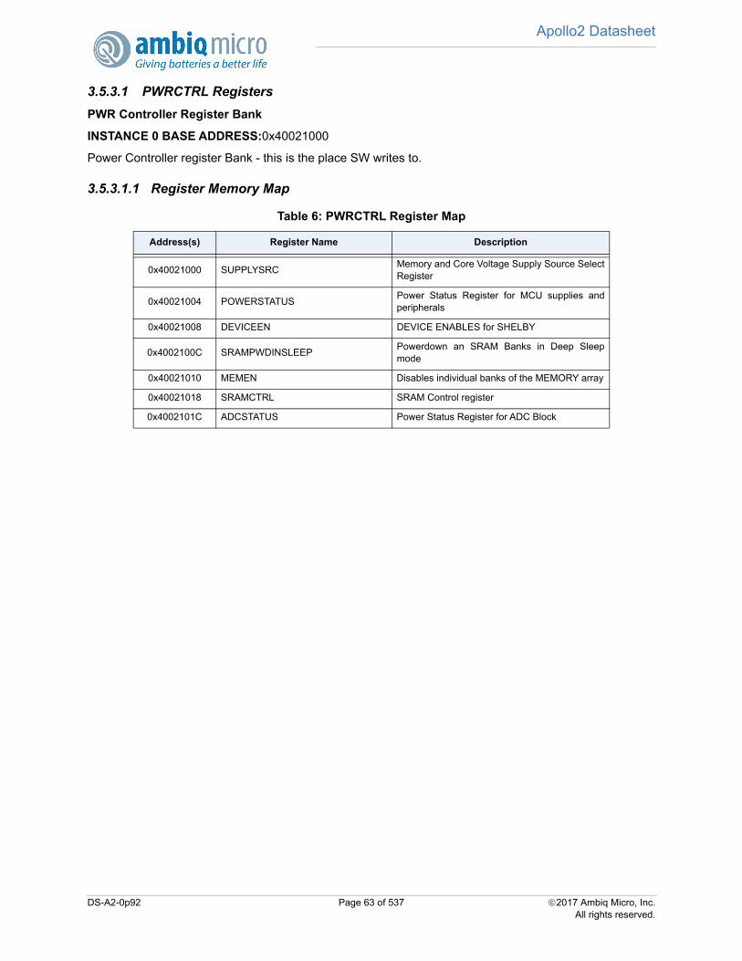
Apollo2 Datasheet
3.5.3.1 PWRCTRL Registers
PWR Controller Register Bank
INSTANCE 0 BASE ADDRESS:0x40021000
Power Controller register Bank - this is the place SW writes to.
3.5.3.1.1 Register Memory Map
Table 6: PWRCTRL Register Map
Address(s) Register Name Description
0x40021000 SUPPLYSRCMemory and Core Voltage Supply Source SelectRegister
0x40021004 POWERSTATUSPower Status Register for MCU supplies andperipherals
0x40021008 DEVICEEN DEVICE ENABLES for SHELBY
0x4002100C SRAMPWDINSLEEPPowerdown an SRAM Banks in Deep Sleepmode
0x40021010 MEMEN Disables individual banks of the MEMORY array
0x40021018 SRAMCTRL SRAM Control register
0x4002101C ADCSTATUS Power Status Register for ADC Block
DS-A2-0p92 Page 63 of 537 2017 Ambiq Micro, Inc.All rights reserved.
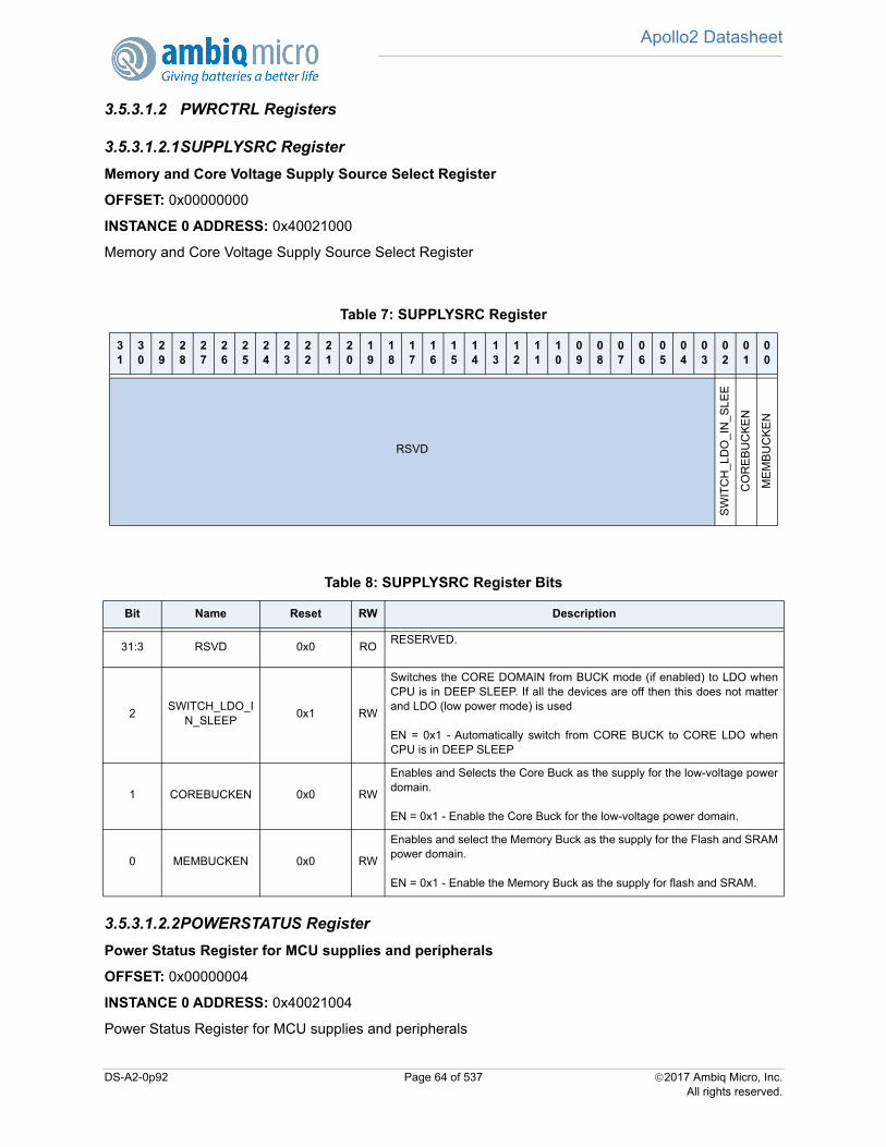
Apollo2 Datasheet
3.5.3.1.2 PWRCTRL Registers
3.5.3.1.2.1SUPPLYSRC Register
Memory and Core Voltage Supply Source Select Register
OFFSET: 0x00000000
INSTANCE 0 ADDRESS: 0x40021000
Memory and Core Voltage Supply Source Select Register
3.5.3.1.2.2POWERSTATUS Register
Power Status Register for MCU supplies and peripherals
OFFSET: 0x00000004
INSTANCE 0 ADDRESS: 0x40021004
Power Status Register for MCU supplies and peripherals
Table 7: SUPPLYSRC Register
31
30
29
28
27
26
25
24
23
22
21
20
19
18
17
16
15
14
13
12
11
10
09
08
07
06
05
04
03
02
01
00
RSVD
SW
ITC
H_L
DO
_IN
_S
LE
E
CO
RE
BU
CK
EN
ME
MB
UC
KE
N
Table 8: SUPPLYSRC Register Bits
Bit Name Reset RW Description
31:3 RSVD 0x0 RORESERVED.
2SWITCH_LDO_I
N_SLEEP0x1 RW
Switches the CORE DOMAIN from BUCK mode (if enabled) to LDO whenCPU is in DEEP SLEEP. If all the devices are off then this does not matterand LDO (low power mode) is used
EN = 0x1 - Automatically switch from CORE BUCK to CORE LDO whenCPU is in DEEP SLEEP
1 COREBUCKEN 0x0 RW
Enables and Selects the Core Buck as the supply for the low-voltage powerdomain.
EN = 0x1 - Enable the Core Buck for the low-voltage power domain.
0 MEMBUCKEN 0x0 RW
Enables and select the Memory Buck as the supply for the Flash and SRAMpower domain.
EN = 0x1 - Enable the Memory Buck as the supply for flash and SRAM.
DS-A2-0p92 Page 64 of 537 2017 Ambiq Micro, Inc.All rights reserved.
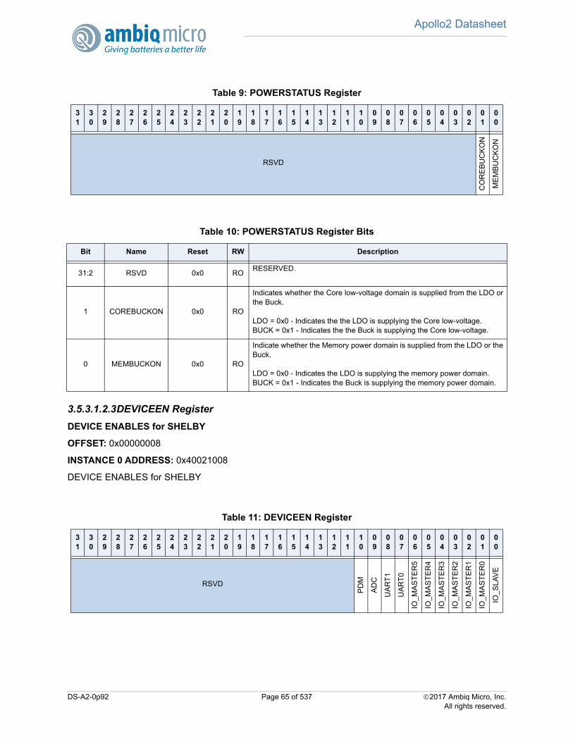
Apollo2 Datasheet
3.5.3.1.2.3DEVICEEN Register
DEVICE ENABLES for SHELBY
OFFSET: 0x00000008
INSTANCE 0 ADDRESS: 0x40021008
DEVICE ENABLES for SHELBY
Table 9: POWERSTATUS Register
31
30
29
28
27
26
25
24
23
22
21
20
19
18
17
16
15
14
13
12
11
10
09
08
07
06
05
04
03
02
01
00
RSVD
CO
RE
BU
CK
ON
ME
MB
UC
KO
N
Table 10: POWERSTATUS Register Bits
Bit Name Reset RW Description
31:2 RSVD 0x0 RORESERVED.
1 COREBUCKON 0x0 RO
Indicates whether the Core low-voltage domain is supplied from the LDO orthe Buck.
LDO = 0x0 - Indicates the the LDO is supplying the Core low-voltage.BUCK = 0x1 - Indicates the the Buck is supplying the Core low-voltage.
0 MEMBUCKON 0x0 RO
Indicate whether the Memory power domain is supplied from the LDO or theBuck.
LDO = 0x0 - Indicates the LDO is supplying the memory power domain.BUCK = 0x1 - Indicates the Buck is supplying the memory power domain.
Table 11: DEVICEEN Register
31
30
29
28
27
26
25
24
23
22
21
20
19
18
17
16
15
14
13
12
11
10
09
08
07
06
05
04
03
02
01
00
RSVD
PD
M
AD
C
UA
RT
1
UA
RT
0
IO_M
AS
TE
R5
IO_M
AS
TE
R4
IO_M
AS
TE
R3
IO_M
AS
TE
R2
IO_M
AS
TE
R1
IO_M
AS
TE
R0
IO_S
LAV
E
DS-A2-0p92 Page 65 of 537 2017 Ambiq Micro, Inc.All rights reserved.

Apollo2 Datasheet
Table 12: DEVICEEN Register Bits
Bit Name Reset RW Description
31:11 RSVD 0x0 RORESERVED.
10 PDM 0x0 RW
Enable PDM Digital Block
EN = 0x1 - Enable PDMDIS = 0x0 - Disables PDM
9 ADC 0x0 RW
Enable ADC Digital Block
EN = 0x1 - Enable ADCDIS = 0x0 - Disables ADC
8 UART1 0x0 RW
Enable UART 1
EN = 0x1 - Enable UART 1DIS = 0x0 - Disables UART 1
7 UART0 0x0 RW
Enable UART 0
EN = 0x1 - Enable UART 0DIS = 0x0 - Disables UART 0
6 IO_MASTER5 0x0 RW
Enable IO MASTER 5
EN = 0x1 - Enable IO MASTER 5DIS = 0x0 - Disables IO MASTER 5
5 IO_MASTER4 0x0 RW
Enable IO MASTER 4
EN = 0x1 - Enable IO MASTER 4DIS = 0x0 - Disables IO MASTER 4
4 IO_MASTER3 0x0 RW
Enable IO MASTER 3
EN = 0x1 - Enable IO MASTER 3DIS = 0x0 - Disables IO MASTER 3
3 IO_MASTER2 0x0 RW
Enable IO MASTER 2
EN = 0x1 - Enable IO MASTER 2DIS = 0x0 - Disables IO MASTER 2
2 IO_MASTER1 0x0 RW
Enable IO MASTER 1
EN = 0x1 - Enable IO MASTER 1DIS = 0x0 - Disables IO MASTER 1
1 IO_MASTER0 0x0 RW
Enable IO MASTER 0
EN = 0x1 - Enable IO MASTER 0DIS = 0x0 - Disables IO MASTER 0
0 IO_SLAVE 0x0 RW
Enable IO SLAVE
EN = 0x1 - Enable IO SLAVEDIS = 0x0 - Disables IO SLAVE
DS-A2-0p92 Page 66 of 537 2017 Ambiq Micro, Inc.All rights reserved.
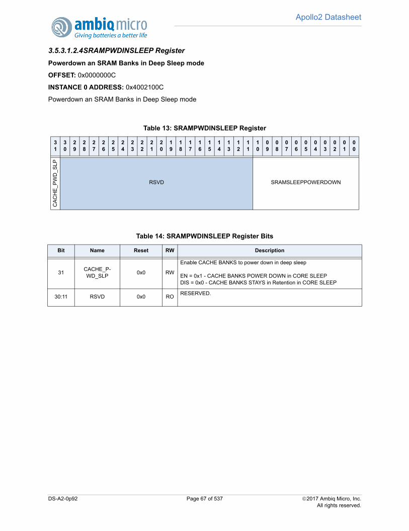
Apollo2 Datasheet
3.5.3.1.2.4SRAMPWDINSLEEP Register
Powerdown an SRAM Banks in Deep Sleep mode
OFFSET: 0x0000000C
INSTANCE 0 ADDRESS: 0x4002100C
Powerdown an SRAM Banks in Deep Sleep mode
Table 13: SRAMPWDINSLEEP Register
31
30
29
28
27
26
25
24
23
22
21
20
19
18
17
16
15
14
13
12
11
10
09
08
07
06
05
04
03
02
01
00
CA
CH
E_
PW
D_
SL
P
RSVD SRAMSLEEPPOWERDOWN
Table 14: SRAMPWDINSLEEP Register Bits
Bit Name Reset RW Description
31CACHE_P-WD_SLP
0x0 RW
Enable CACHE BANKS to power down in deep sleep
EN = 0x1 - CACHE BANKS POWER DOWN in CORE SLEEPDIS = 0x0 - CACHE BANKS STAYS in Retention in CORE SLEEP
30:11 RSVD 0x0 RORESERVED.
DS-A2-0p92 Page 67 of 537 2017 Ambiq Micro, Inc.All rights reserved.

Apollo2 Datasheet
3.5.3.1.2.5MEMEN Register
Disables individual banks of the MEMORY array
OFFSET: 0x00000010
INSTANCE 0 ADDRESS: 0x40021010
Disables individual banks of the MEMORY array
10:0SRAMSLEEP-POWERDOWN
0x0 RW
Selects which SRAM banks are powered down in deep sleep mode, causingthe contents of the bank to be lost.
NONE = 0x0 - All banks retainedGROUP0_SRAM0 = 0x1 - 0KB-8KB SRAMGROUP0_SRAM1 = 0x2 - 8KB-16KB SRAMGROUP0_SRAM2 = 0x4 - 16KB-24KB SRAMGROUP0_SRAM3 = 0x8 - 24KB-32KB SRAMGROUP1 = 0x10 - 32KB-64KB SRAMsGROUP2 = 0x20 - 64KB-96KB SRAMsGROUP3 = 0x40 - 96KB-128KB SRAMsGROUP4 = 0x80 - 128KB-160KB SRAMsGROUP5 = 0x100 - 160KB-192KB SRAMsGROUP6 = 0x200 - 192KB-224KB SRAMsGROUP7 = 0x400 - 224KB-256KB SRAMsSRAM8K = 0x1 - Do not Retain lower 8KBSRAM16K = 0x3 - Do not Retain lower 16KBSRAM32K = 0xF - Do not Retain lower 32KBSRAM64K = 0x1F - Do not Retain lower 64KBSRAM128K = 0x7F - Do not Retain lower 128KBALLBUTLOWER8K = 0x7FE - All banks but lower 8k powered down.ALLBUTLOWER16K = 0x7FC - All banks but lower 16k powered down.ALLBUTLOWER24K = 0x7F8 - All banks but lower 24k powered down.ALLBUTLOWER32K = 0x7F0 - All banks but lower 32k powered down.ALLBUTLOWER64K = 0x7E0 - All banks but lower 64k powered down.ALLBUTLOWER128K = 0x780 - All banks but lower 128k powered down.ALL = 0x7FF - All banks powered down.
Table 15: MEMEN Register
31
30
29
28
27
26
25
24
23
22
21
20
19
18
17
16
15
14
13
12
11
10
09
08
07
06
05
04
03
02
01
00
CA
CH
EB
2
RS
VD
CA
CH
EB
0
RSVD
FLA
SH
1
FLA
SH
0
SRAMEN
Table 14: SRAMPWDINSLEEP Register Bits
Bit Name Reset RW Description
DS-A2-0p92 Page 68 of 537 2017 Ambiq Micro, Inc.All rights reserved.
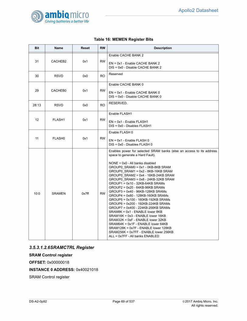
Apollo2 Datasheet
3.5.3.1.2.6SRAMCTRL Register
SRAM Control register
OFFSET: 0x00000018
INSTANCE 0 ADDRESS: 0x40021018
SRAM Control register
Table 16: MEMEN Register Bits
Bit Name Reset RW Description
31 CACHEB2 0x1 RW
Enable CACHE BANK 2
EN = 0x1 - Enable CACHE BANK 2DIS = 0x0 - Disable CACHE BANK 2
30 RSVD 0x0 ROReserved
29 CACHEB0 0x1 RW
Enable CACHE BANK 0
EN = 0x1 - Enable CACHE BANK 0DIS = 0x0 - Disable CACHE BANK 0
28:13 RSVD 0x0 RORESERVED.
12 FLASH1 0x1 RW
Enable FLASH1
EN = 0x1 - Enable FLASH1DIS = 0x0 - Disables FLASH1
11 FLASH0 0x1 RW
Enable FLASH 0
EN = 0x1 - Enable FLASH 0DIS = 0x0 - Disables FLASH 0
10:0 SRAMEN 0x7ff RW
Enables power for selected SRAM banks (else an access to its addressspace to generate a Hard Fault).
NONE = 0x0 - All banks disabledGROUP0_SRAM0 = 0x1 - 0KB-8KB SRAMGROUP0_SRAM1 = 0x2 - 8KB-16KB SRAMGROUP0_SRAM2 = 0x4 - 16KB-24KB SRAMGROUP0_SRAM3 = 0x8 - 24KB-32KB SRAMGROUP1 = 0x10 - 32KB-64KB SRAMsGROUP2 = 0x20 - 64KB-96KB SRAMsGROUP3 = 0x40 - 96KB-128KB SRAMsGROUP4 = 0x80 - 128KB-160KB SRAMsGROUP5 = 0x100 - 160KB-192KB SRAMsGROUP6 = 0x200 - 192KB-224KB SRAMsGROUP7 = 0x400 - 224KB-256KB SRAMsSRAM8K = 0x1 - ENABLE lower 8KBSRAM16K = 0x3 - ENABLE lower 16KBSRAM32K = 0xF - ENABLE lower 32KBSRAM64K = 0x1F - ENABLE lower 64KBSRAM128K = 0x7F - ENABLE lower 128KBSRAM256K = 0x7FF - ENABLE lower 256KBALL = 0x7FF - All banks ENABLED
DS-A2-0p92 Page 69 of 537 2017 Ambiq Micro, Inc.All rights reserved.

Apollo2 Datasheet
3.5.3.1.2.7ADCSTATUS Register
Power Status Register for ADC Block
OFFSET: 0x0000001C
INSTANCE 0 ADDRESS: 0x4002101C
Power Status Register for ADC Block
Table 17: SRAMCTRL Register
31
30
29
28
27
26
25
24
23
22
21
20
19
18
17
16
15
14
13
12
11
10
09
08
07
06
05
04
03
02
01
00
RSVD
SR
AM
_MA
ST
ER
_CLK
GA
TE
SR
AM
_CLK
GA
TE
SR
AM
_LIG
HT
_SLE
EP
Table 18: SRAMCTRL Register Bits
Bit Name Reset RW Description
31:3 RSVD 0x0 ROThis bitfield is reserved for future use.
2SRAM_MAS-
TER_CLKGATE0x0 RW
Enables top-level clock gating in the SRAM block. This bit should beenabled for lowest power operation.
EN = 0x1 - Enable Master SRAM Clock GateDIS = 0x0 - Disables Master SRAM Clock Gating
1SRAM_CLK-
GATE0x0 RW
Enables individual per-RAM clock gating in the SRAM block. This bit shouldbe enabled for lowest power operation.
EN = 0x1 - Enable Individual SRAM Clock GatingDIS = 0x0 - Disables Individual SRAM Clock Gating
0SRAM_LIGHT_
SLEEP0x1 RW
Enable LS (light sleep) of cache RAMs. When this bit is set, the RAMS willbe put into light sleep mode while inactive. NOTE: if the SRAM is activelyused, this may have an adverse affect on power since entering/exiting LSmode may consume more power than would be saved.
EN = 0x1 - Enable LIGHT SLEEP for SRAMsDIS = 0x0 - Disables LIGHT SLEEP for SRAMs
DS-A2-0p92 Page 70 of 537 2017 Ambiq Micro, Inc.All rights reserved.
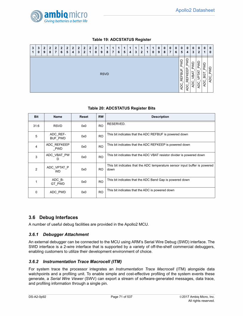
Apollo2 Datasheet
3.6 Debug InterfacesA number of useful debug facilities are provided in the Apollo2 MCU.
3.6.1 Debugger Attachment
An external debugger can be connected to the MCU using ARM’s Serial Wire Debug (SWD) interface. TheSWD interface is a 2-wire interface that is supported by a variety of off-the-shelf commercial debuggers,enabling customers to utilize their development environment of choice.
3.6.2 Instrumentation Trace Macrocell (ITM)
For system trace the processor integrates an Instrumentation Trace Macrocell (ITM) alongside datawatchpoints and a profiling unit. To enable simple and cost-effective profiling of the system events thesegenerate, a Serial Wire Viewer (SWV) can export a stream of software-generated messages, data trace,and profiling information through a single pin.
Table 19: ADCSTATUS Register
31
30
29
28
27
26
25
24
23
22
21
20
19
18
17
16
15
14
13
12
11
10
09
08
07
06
05
04
03
02
01
00
RSVD
AD
C_R
EF
BU
F_P
WD
AD
C_R
EF
KE
EP
_PW
D
AD
C_
VB
AT
_PW
D
AD
C_V
PTA
T_P
WD
AD
C_
BG
T_
PW
D
AD
C_
PW
D
Table 20: ADCSTATUS Register Bits
Bit Name Reset RW Description
31:6 RSVD 0x0 RORESERVED.
5ADC_REF-BUF_PWD
0x0 ROThis bit indicates that the ADC REFBUF is powered down
4ADC_REFKEEP
_PWD0x0 RO
This bit indicates that the ADC REFKEEP is powered down
3ADC_VBAT_PW
D0x0 RO
This bit indicates that the ADC VBAT resistor divider is powered down
2ADC_VPTAT_P
WD0x0 RO
This bit indicates that the ADC temperature sensor input buffer is powereddown
1ADC_B-
GT_PWD0x0 RO
This bit indicates that the ADC Band Gap is powered down
0 ADC_PWD 0x0 ROThis bit indicates that the ADC is powered down
DS-A2-0p92 Page 71 of 537 2017 Ambiq Micro, Inc.All rights reserved.

Apollo2 Datasheet
3.6.3 Trace Port Interface Unit (TPIU)
The Apollo2 MCU includes a Cortex-M4 Trace Port Interface Unit (TPIU). The Cortex-M4 TPIU is an ARMIP component that acts as a bridge between the on-chip trace data from the ITM and the single pinsupporting the Serial Wire Viewer Protocol.
The TPIU includes a Trace Output Serializer that can format and send the SWV protocol in either aManchester encoded form or as a standard UART stream.
3.6.4 Faulting Address Trapping Hardware
The Apollo2 MCU offers an optional facility for trapping the address associated with bus faults occurring onany of the three AMBA AHB buses on the chip. This facility must be specifically enabled so that energy isnot wasted when one is not actively debugging.
3.7 ITM RegistersARM ITM Registers.
INSTANCE 0 BASE ADDRESS:0x00000000
DS-A2-0p92 Page 72 of 537 2017 Ambiq Micro, Inc.All rights reserved.
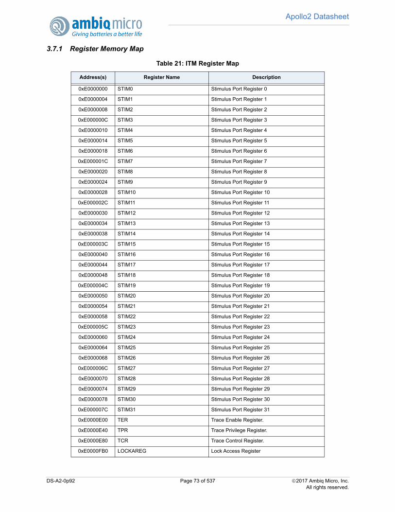
Apollo2 Datasheet
3.7.1 Register Memory Map
Table 21: ITM Register Map
Address(s) Register Name Description
0xE0000000 STIM0 Stimulus Port Register 0
0xE0000004 STIM1 Stimulus Port Register 1
0xE0000008 STIM2 Stimulus Port Register 2
0xE000000C STIM3 Stimulus Port Register 3
0xE0000010 STIM4 Stimulus Port Register 4
0xE0000014 STIM5 Stimulus Port Register 5
0xE0000018 STIM6 Stimulus Port Register 6
0xE000001C STIM7 Stimulus Port Register 7
0xE0000020 STIM8 Stimulus Port Register 8
0xE0000024 STIM9 Stimulus Port Register 9
0xE0000028 STIM10 Stimulus Port Register 10
0xE000002C STIM11 Stimulus Port Register 11
0xE0000030 STIM12 Stimulus Port Register 12
0xE0000034 STIM13 Stimulus Port Register 13
0xE0000038 STIM14 Stimulus Port Register 14
0xE000003C STIM15 Stimulus Port Register 15
0xE0000040 STIM16 Stimulus Port Register 16
0xE0000044 STIM17 Stimulus Port Register 17
0xE0000048 STIM18 Stimulus Port Register 18
0xE000004C STIM19 Stimulus Port Register 19
0xE0000050 STIM20 Stimulus Port Register 20
0xE0000054 STIM21 Stimulus Port Register 21
0xE0000058 STIM22 Stimulus Port Register 22
0xE000005C STIM23 Stimulus Port Register 23
0xE0000060 STIM24 Stimulus Port Register 24
0xE0000064 STIM25 Stimulus Port Register 25
0xE0000068 STIM26 Stimulus Port Register 26
0xE000006C STIM27 Stimulus Port Register 27
0xE0000070 STIM28 Stimulus Port Register 28
0xE0000074 STIM29 Stimulus Port Register 29
0xE0000078 STIM30 Stimulus Port Register 30
0xE000007C STIM31 Stimulus Port Register 31
0xE0000E00 TER Trace Enable Register.
0xE0000E40 TPR Trace Privilege Register.
0xE0000E80 TCR Trace Control Register.
0xE0000FB0 LOCKAREG Lock Access Register
DS-A2-0p92 Page 73 of 537 2017 Ambiq Micro, Inc.All rights reserved.
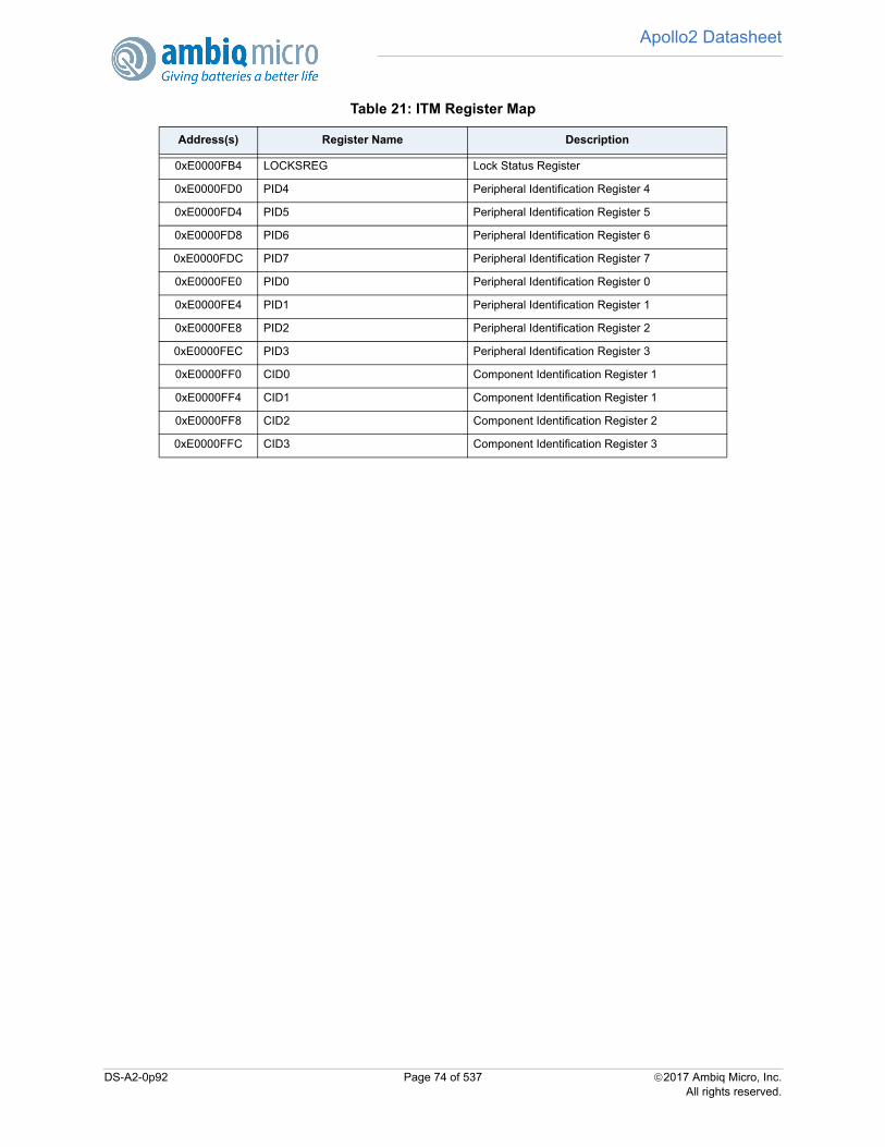
Apollo2 Datasheet
0xE0000FB4 LOCKSREG Lock Status Register
0xE0000FD0 PID4 Peripheral Identification Register 4
0xE0000FD4 PID5 Peripheral Identification Register 5
0xE0000FD8 PID6 Peripheral Identification Register 6
0xE0000FDC PID7 Peripheral Identification Register 7
0xE0000FE0 PID0 Peripheral Identification Register 0
0xE0000FE4 PID1 Peripheral Identification Register 1
0xE0000FE8 PID2 Peripheral Identification Register 2
0xE0000FEC PID3 Peripheral Identification Register 3
0xE0000FF0 CID0 Component Identification Register 1
0xE0000FF4 CID1 Component Identification Register 1
0xE0000FF8 CID2 Component Identification Register 2
0xE0000FFC CID3 Component Identification Register 3
Table 21: ITM Register Map
Address(s) Register Name Description
DS-A2-0p92 Page 74 of 537 2017 Ambiq Micro, Inc.All rights reserved.
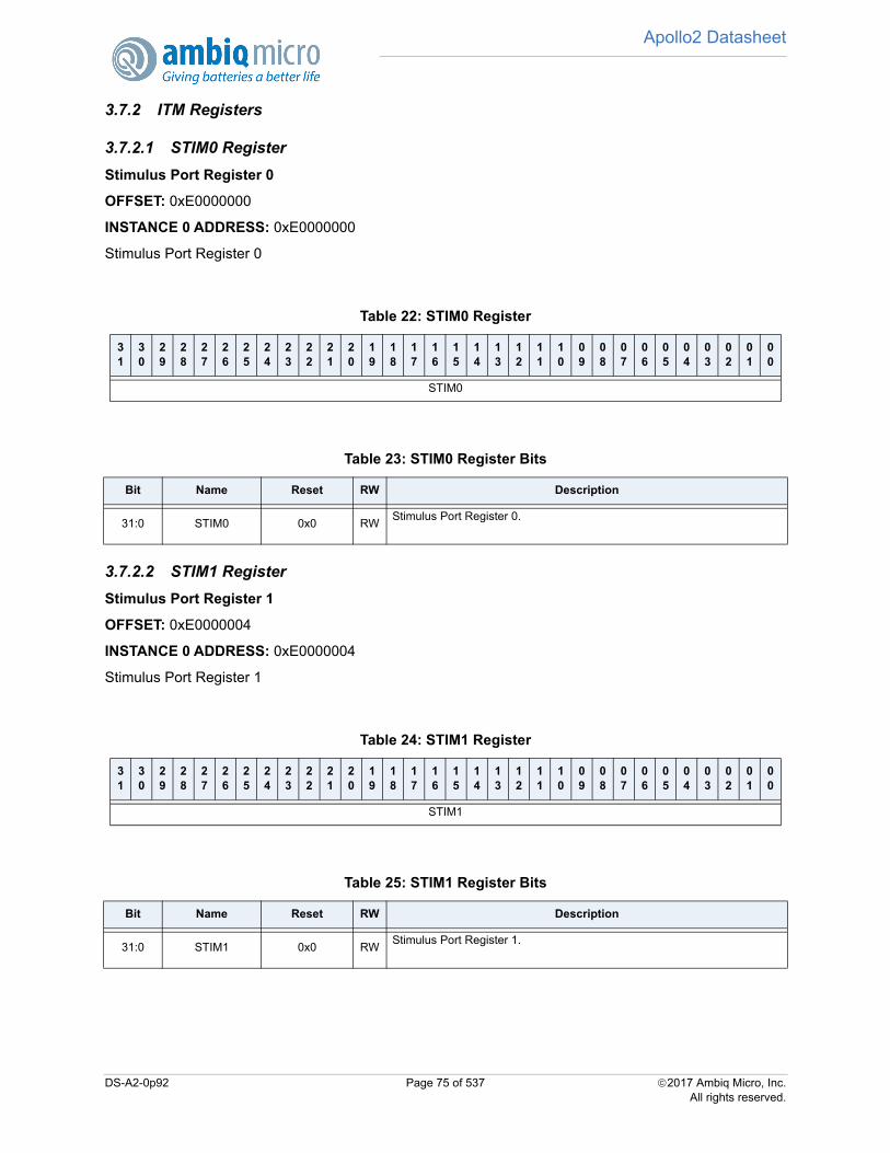
Apollo2 Datasheet
3.7.2 ITM Registers
3.7.2.1 STIM0 Register
Stimulus Port Register 0
OFFSET: 0xE0000000
INSTANCE 0 ADDRESS: 0xE0000000
Stimulus Port Register 0
3.7.2.2 STIM1 Register
Stimulus Port Register 1
OFFSET: 0xE0000004
INSTANCE 0 ADDRESS: 0xE0000004
Stimulus Port Register 1
Table 22: STIM0 Register
31
30
29
28
27
26
25
24
23
22
21
20
19
18
17
16
15
14
13
12
11
10
09
08
07
06
05
04
03
02
01
00
STIM0
Table 23: STIM0 Register Bits
Bit Name Reset RW Description
31:0 STIM0 0x0 RWStimulus Port Register 0.
Table 24: STIM1 Register
31
30
29
28
27
26
25
24
23
22
21
20
19
18
17
16
15
14
13
12
11
10
09
08
07
06
05
04
03
02
01
00
STIM1
Table 25: STIM1 Register Bits
Bit Name Reset RW Description
31:0 STIM1 0x0 RWStimulus Port Register 1.
DS-A2-0p92 Page 75 of 537 2017 Ambiq Micro, Inc.All rights reserved.
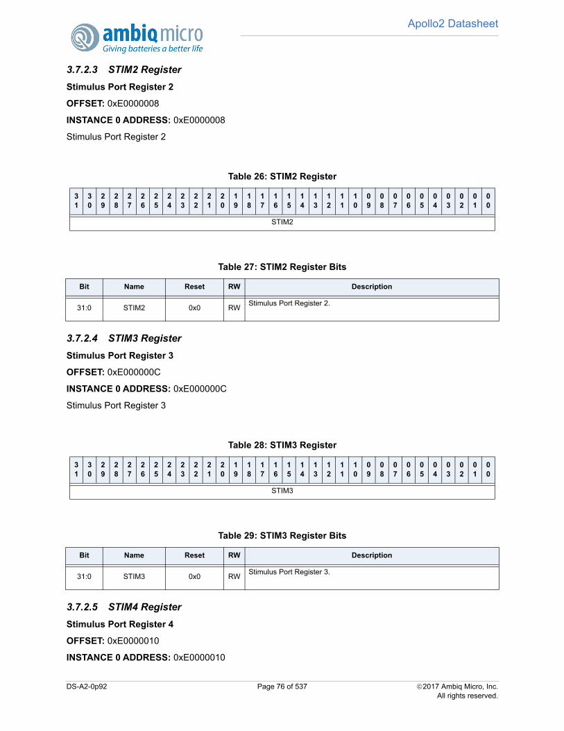
Apollo2 Datasheet
3.7.2.3 STIM2 Register
Stimulus Port Register 2
OFFSET: 0xE0000008
INSTANCE 0 ADDRESS: 0xE0000008
Stimulus Port Register 2
3.7.2.4 STIM3 Register
Stimulus Port Register 3
OFFSET: 0xE000000C
INSTANCE 0 ADDRESS: 0xE000000C
Stimulus Port Register 3
3.7.2.5 STIM4 Register
Stimulus Port Register 4
OFFSET: 0xE0000010
INSTANCE 0 ADDRESS: 0xE0000010
Table 26: STIM2 Register
31
30
29
28
27
26
25
24
23
22
21
20
19
18
17
16
15
14
13
12
11
10
09
08
07
06
05
04
03
02
01
00
STIM2
Table 27: STIM2 Register Bits
Bit Name Reset RW Description
31:0 STIM2 0x0 RWStimulus Port Register 2.
Table 28: STIM3 Register
31
30
29
28
27
26
25
24
23
22
21
20
19
18
17
16
15
14
13
12
11
10
09
08
07
06
05
04
03
02
01
00
STIM3
Table 29: STIM3 Register Bits
Bit Name Reset RW Description
31:0 STIM3 0x0 RWStimulus Port Register 3.
DS-A2-0p92 Page 76 of 537 2017 Ambiq Micro, Inc.All rights reserved.
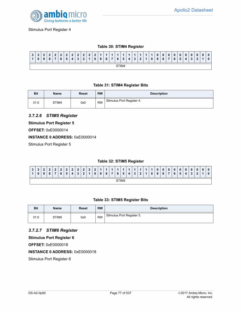
Apollo2 Datasheet
Stimulus Port Register 4
3.7.2.6 STIM5 Register
Stimulus Port Register 5
OFFSET: 0xE0000014
INSTANCE 0 ADDRESS: 0xE0000014
Stimulus Port Register 5
3.7.2.7 STIM6 Register
Stimulus Port Register 6
OFFSET: 0xE0000018
INSTANCE 0 ADDRESS: 0xE0000018
Stimulus Port Register 6
Table 30: STIM4 Register
31
30
29
28
27
26
25
24
23
22
21
20
19
18
17
16
15
14
13
12
11
10
09
08
07
06
05
04
03
02
01
00
STIM4
Table 31: STIM4 Register Bits
Bit Name Reset RW Description
31:0 STIM4 0x0 RWStimulus Port Register 4.
Table 32: STIM5 Register
31
30
29
28
27
26
25
24
23
22
21
20
19
18
17
16
15
14
13
12
11
10
09
08
07
06
05
04
03
02
01
00
STIM5
Table 33: STIM5 Register Bits
Bit Name Reset RW Description
31:0 STIM5 0x0 RWStimulus Port Register 5.
DS-A2-0p92 Page 77 of 537 2017 Ambiq Micro, Inc.All rights reserved.

Apollo2 Datasheet
3.7.2.8 STIM7 Register
Stimulus Port Register 7
OFFSET: 0xE000001C
INSTANCE 0 ADDRESS: 0xE000001C
Stimulus Port Register 7
3.7.2.9 STIM8 Register
Stimulus Port Register 8
OFFSET: 0xE0000020
INSTANCE 0 ADDRESS: 0xE0000020
Stimulus Port Register 8
Table 34: STIM6 Register
31
30
29
28
27
26
25
24
23
22
21
20
19
18
17
16
15
14
13
12
11
10
09
08
07
06
05
04
03
02
01
00
STIM6
Table 35: STIM6 Register Bits
Bit Name Reset RW Description
31:0 STIM6 0x0 RWStimulus Port Register 6.
Table 36: STIM7 Register
31
30
29
28
27
26
25
24
23
22
21
20
19
18
17
16
15
14
13
12
11
10
09
08
07
06
05
04
03
02
01
00
STIM7
Table 37: STIM7 Register Bits
Bit Name Reset RW Description
31:0 STIM7 0x0 RWStimulus Port Register 7.
DS-A2-0p92 Page 78 of 537 2017 Ambiq Micro, Inc.All rights reserved.

Apollo2 Datasheet
3.7.2.10 STIM9 Register
Stimulus Port Register 9
OFFSET: 0xE0000024
INSTANCE 0 ADDRESS: 0xE0000024
Stimulus Port Register 9
3.7.2.11 STIM10 Register
Stimulus Port Register 10
OFFSET: 0xE0000028
INSTANCE 0 ADDRESS: 0xE0000028
Stimulus Port Register 10
Table 38: STIM8 Register
31
30
29
28
27
26
25
24
23
22
21
20
19
18
17
16
15
14
13
12
11
10
09
08
07
06
05
04
03
02
01
00
STIM8
Table 39: STIM8 Register Bits
Bit Name Reset RW Description
31:0 STIM8 0x0 RWStimulus Port Register 8.
Table 40: STIM9 Register
31
30
29
28
27
26
25
24
23
22
21
20
19
18
17
16
15
14
13
12
11
10
09
08
07
06
05
04
03
02
01
00
STIM9
Table 41: STIM9 Register Bits
Bit Name Reset RW Description
31:0 STIM9 0x0 RWStimulus Port Register 9.
DS-A2-0p92 Page 79 of 537 2017 Ambiq Micro, Inc.All rights reserved.

Apollo2 Datasheet
3.7.2.12 STIM11 Register
Stimulus Port Register 11
OFFSET: 0xE000002C
INSTANCE 0 ADDRESS: 0xE000002C
Stimulus Port Register 11
3.7.2.13 STIM12 Register
Stimulus Port Register 12
OFFSET: 0xE0000030
INSTANCE 0 ADDRESS: 0xE0000030
Stimulus Port Register 12
Table 42: STIM10 Register
31
30
29
28
27
26
25
24
23
22
21
20
19
18
17
16
15
14
13
12
11
10
09
08
07
06
05
04
03
02
01
00
STIM10
Table 43: STIM10 Register Bits
Bit Name Reset RW Description
31:0 STIM10 0x0 RWStimulus Port Register 10.
Table 44: STIM11 Register
31
30
29
28
27
26
25
24
23
22
21
20
19
18
17
16
15
14
13
12
11
10
09
08
07
06
05
04
03
02
01
00
STIM11
Table 45: STIM11 Register Bits
Bit Name Reset RW Description
31:0 STIM11 0x0 RWStimulus Port Register 11.
DS-A2-0p92 Page 80 of 537 2017 Ambiq Micro, Inc.All rights reserved.

Apollo2 Datasheet
3.7.2.14 STIM13 Register
Stimulus Port Register 13
OFFSET: 0xE0000034
INSTANCE 0 ADDRESS: 0xE0000034
Stimulus Port Register 13
3.7.2.15 STIM14 Register
Stimulus Port Register 14
OFFSET: 0xE0000038
INSTANCE 0 ADDRESS: 0xE0000038
Stimulus Port Register 14
Table 46: STIM12 Register
31
30
29
28
27
26
25
24
23
22
21
20
19
18
17
16
15
14
13
12
11
10
09
08
07
06
05
04
03
02
01
00
STIM12
Table 47: STIM12 Register Bits
Bit Name Reset RW Description
31:0 STIM12 0x0 RWStimulus Port Register 12.
Table 48: STIM13 Register
31
30
29
28
27
26
25
24
23
22
21
20
19
18
17
16
15
14
13
12
11
10
09
08
07
06
05
04
03
02
01
00
STIM13
Table 49: STIM13 Register Bits
Bit Name Reset RW Description
31:0 STIM13 0x0 RWStimulus Port Register 13.
DS-A2-0p92 Page 81 of 537 2017 Ambiq Micro, Inc.All rights reserved.

Apollo2 Datasheet
3.7.2.16 STIM15 Register
Stimulus Port Register 15
OFFSET: 0xE000003C
INSTANCE 0 ADDRESS: 0xE000003C
Stimulus Port Register 15
3.7.2.17 STIM16 Register
Stimulus Port Register 16
OFFSET: 0xE0000040
INSTANCE 0 ADDRESS: 0xE0000040
Stimulus Port Register 16
Table 50: STIM14 Register
31
30
29
28
27
26
25
24
23
22
21
20
19
18
17
16
15
14
13
12
11
10
09
08
07
06
05
04
03
02
01
00
STIM14
Table 51: STIM14 Register Bits
Bit Name Reset RW Description
31:0 STIM14 0x0 RWStimulus Port Register 14.
Table 52: STIM15 Register
31
30
29
28
27
26
25
24
23
22
21
20
19
18
17
16
15
14
13
12
11
10
09
08
07
06
05
04
03
02
01
00
STIM15
Table 53: STIM15 Register Bits
Bit Name Reset RW Description
31:0 STIM15 0x0 RWStimulus Port Register 15.
DS-A2-0p92 Page 82 of 537 2017 Ambiq Micro, Inc.All rights reserved.

Apollo2 Datasheet
3.7.2.18 STIM17 Register
Stimulus Port Register 17
OFFSET: 0xE0000044
INSTANCE 0 ADDRESS: 0xE0000044
Stimulus Port Register 17
3.7.2.19 STIM18 Register
Stimulus Port Register 18
OFFSET: 0xE0000048
INSTANCE 0 ADDRESS: 0xE0000048
Stimulus Port Register 18
Table 54: STIM16 Register
31
30
29
28
27
26
25
24
23
22
21
20
19
18
17
16
15
14
13
12
11
10
09
08
07
06
05
04
03
02
01
00
STIM16
Table 55: STIM16 Register Bits
Bit Name Reset RW Description
31:0 STIM16 0x0 RWStimulus Port Register 16.
Table 56: STIM17 Register
31
30
29
28
27
26
25
24
23
22
21
20
19
18
17
16
15
14
13
12
11
10
09
08
07
06
05
04
03
02
01
00
STIM17
Table 57: STIM17 Register Bits
Bit Name Reset RW Description
31:0 STIM17 0x0 RWStimulus Port Register 17.
DS-A2-0p92 Page 83 of 537 2017 Ambiq Micro, Inc.All rights reserved.

Apollo2 Datasheet
3.7.2.20 STIM19 Register
Stimulus Port Register 19
OFFSET: 0xE000004C
INSTANCE 0 ADDRESS: 0xE000004C
Stimulus Port Register 19
3.7.2.21 STIM20 Register
Stimulus Port Register 20
OFFSET: 0xE0000050
INSTANCE 0 ADDRESS: 0xE0000050
Stimulus Port Register 20
Table 58: STIM18 Register
31
30
29
28
27
26
25
24
23
22
21
20
19
18
17
16
15
14
13
12
11
10
09
08
07
06
05
04
03
02
01
00
STIM18
Table 59: STIM18 Register Bits
Bit Name Reset RW Description
31:0 STIM18 0x0 RWStimulus Port Register 18.
Table 60: STIM19 Register
31
30
29
28
27
26
25
24
23
22
21
20
19
18
17
16
15
14
13
12
11
10
09
08
07
06
05
04
03
02
01
00
STIM19
Table 61: STIM19 Register Bits
Bit Name Reset RW Description
31:0 STIM19 0x0 RWStimulus Port Register 19.
DS-A2-0p92 Page 84 of 537 2017 Ambiq Micro, Inc.All rights reserved.

Apollo2 Datasheet
3.7.2.22 STIM21 Register
Stimulus Port Register 21
OFFSET: 0xE0000054
INSTANCE 0 ADDRESS: 0xE0000054
Stimulus Port Register 21
3.7.2.23 STIM22 Register
Stimulus Port Register 22
OFFSET: 0xE0000058
INSTANCE 0 ADDRESS: 0xE0000058
Stimulus Port Register 22
Table 62: STIM20 Register
31
30
29
28
27
26
25
24
23
22
21
20
19
18
17
16
15
14
13
12
11
10
09
08
07
06
05
04
03
02
01
00
STIM20
Table 63: STIM20 Register Bits
Bit Name Reset RW Description
31:0 STIM20 0x0 RWStimulus Port Register 20.
Table 64: STIM21 Register
31
30
29
28
27
26
25
24
23
22
21
20
19
18
17
16
15
14
13
12
11
10
09
08
07
06
05
04
03
02
01
00
STIM21
Table 65: STIM21 Register Bits
Bit Name Reset RW Description
31:0 STIM21 0x0 RWStimulus Port Register 21.
DS-A2-0p92 Page 85 of 537 2017 Ambiq Micro, Inc.All rights reserved.

Apollo2 Datasheet
3.7.2.24 STIM23 Register
Stimulus Port Register 23
OFFSET: 0xE000005C
INSTANCE 0 ADDRESS: 0xE000005C
Stimulus Port Register 23
3.7.2.25 STIM24 Register
Stimulus Port Register 24
OFFSET: 0xE0000060
INSTANCE 0 ADDRESS: 0xE0000060
Stimulus Port Register 24
Table 66: STIM22 Register
31
30
29
28
27
26
25
24
23
22
21
20
19
18
17
16
15
14
13
12
11
10
09
08
07
06
05
04
03
02
01
00
STIM22
Table 67: STIM22 Register Bits
Bit Name Reset RW Description
31:0 STIM22 0x0 RWStimulus Port Register 22.
Table 68: STIM23 Register
31
30
29
28
27
26
25
24
23
22
21
20
19
18
17
16
15
14
13
12
11
10
09
08
07
06
05
04
03
02
01
00
STIM23
Table 69: STIM23 Register Bits
Bit Name Reset RW Description
31:0 STIM23 0x0 RWStimulus Port Register 23.
DS-A2-0p92 Page 86 of 537 2017 Ambiq Micro, Inc.All rights reserved.
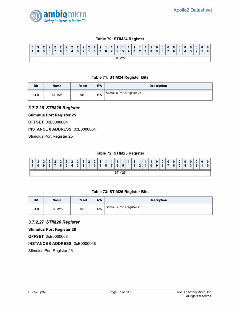
Apollo2 Datasheet
3.7.2.26 STIM25 Register
Stimulus Port Register 25
OFFSET: 0xE0000064
INSTANCE 0 ADDRESS: 0xE0000064
Stimulus Port Register 25
3.7.2.27 STIM26 Register
Stimulus Port Register 26
OFFSET: 0xE0000068
INSTANCE 0 ADDRESS: 0xE0000068
Stimulus Port Register 26
Table 70: STIM24 Register
31
30
29
28
27
26
25
24
23
22
21
20
19
18
17
16
15
14
13
12
11
10
09
08
07
06
05
04
03
02
01
00
STIM24
Table 71: STIM24 Register Bits
Bit Name Reset RW Description
31:0 STIM24 0x0 RWStimulus Port Register 24.
Table 72: STIM25 Register
31
30
29
28
27
26
25
24
23
22
21
20
19
18
17
16
15
14
13
12
11
10
09
08
07
06
05
04
03
02
01
00
STIM25
Table 73: STIM25 Register Bits
Bit Name Reset RW Description
31:0 STIM25 0x0 RWStimulus Port Register 25.
DS-A2-0p92 Page 87 of 537 2017 Ambiq Micro, Inc.All rights reserved.

Apollo2 Datasheet
3.7.2.28 STIM27 Register
Stimulus Port Register 27
OFFSET: 0xE000006C
INSTANCE 0 ADDRESS: 0xE000006C
Stimulus Port Register 27
3.7.2.29 STIM28 Register
Stimulus Port Register 28
OFFSET: 0xE0000070
INSTANCE 0 ADDRESS: 0xE0000070
Stimulus Port Register 28
Table 74: STIM26 Register
31
30
29
28
27
26
25
24
23
22
21
20
19
18
17
16
15
14
13
12
11
10
09
08
07
06
05
04
03
02
01
00
STIM26
Table 75: STIM26 Register Bits
Bit Name Reset RW Description
31:0 STIM26 0x0 RWStimulus Port Register 26.
Table 76: STIM27 Register
31
30
29
28
27
26
25
24
23
22
21
20
19
18
17
16
15
14
13
12
11
10
09
08
07
06
05
04
03
02
01
00
STIM27
Table 77: STIM27 Register Bits
Bit Name Reset RW Description
31:0 STIM27 0x0 RWStimulus Port Register 27.
DS-A2-0p92 Page 88 of 537 2017 Ambiq Micro, Inc.All rights reserved.

Apollo2 Datasheet
3.7.2.30 STIM29 Register
Stimulus Port Register 29
OFFSET: 0xE0000074
INSTANCE 0 ADDRESS: 0xE0000074
Stimulus Port Register 29
3.7.2.31 STIM30 Register
Stimulus Port Register 30
OFFSET: 0xE0000078
INSTANCE 0 ADDRESS: 0xE0000078
Stimulus Port Register 30
Table 78: STIM28 Register
31
30
29
28
27
26
25
24
23
22
21
20
19
18
17
16
15
14
13
12
11
10
09
08
07
06
05
04
03
02
01
00
STIM28
Table 79: STIM28 Register Bits
Bit Name Reset RW Description
31:0 STIM28 0x0 RWStimulus Port Register 28.
Table 80: STIM29 Register
31
30
29
28
27
26
25
24
23
22
21
20
19
18
17
16
15
14
13
12
11
10
09
08
07
06
05
04
03
02
01
00
STIM29
Table 81: STIM29 Register Bits
Bit Name Reset RW Description
31:0 STIM29 0x0 RWStimulus Port Register 29.
DS-A2-0p92 Page 89 of 537 2017 Ambiq Micro, Inc.All rights reserved.

Apollo2 Datasheet
3.7.2.32 STIM31 Register
Stimulus Port Register 31
OFFSET: 0xE000007C
INSTANCE 0 ADDRESS: 0xE000007C
Stimulus Port Register 31
3.7.2.33 TER Register
Trace Enable Register.
OFFSET: 0xE0000E00
INSTANCE 0 ADDRESS: 0xE0000E00
Trace Enable Register.
Table 82: STIM30 Register
31
30
29
28
27
26
25
24
23
22
21
20
19
18
17
16
15
14
13
12
11
10
09
08
07
06
05
04
03
02
01
00
STIM30
Table 83: STIM30 Register Bits
Bit Name Reset RW Description
31:0 STIM30 0x0 RWStimulus Port Register 30.
Table 84: STIM31 Register
31
30
29
28
27
26
25
24
23
22
21
20
19
18
17
16
15
14
13
12
11
10
09
08
07
06
05
04
03
02
01
00
STIM31
Table 85: STIM31 Register Bits
Bit Name Reset RW Description
31:0 STIM31 0x0 RWStimulus Port Register 31.
DS-A2-0p92 Page 90 of 537 2017 Ambiq Micro, Inc.All rights reserved.
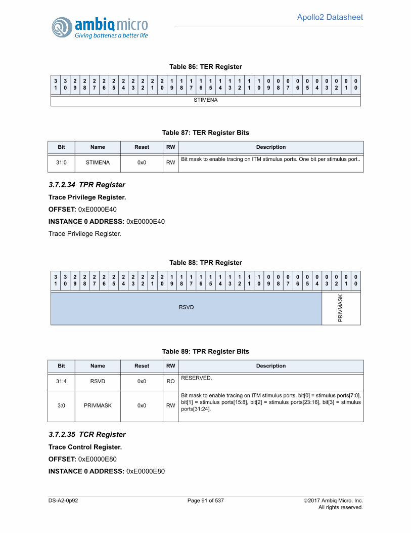
Apollo2 Datasheet
3.7.2.34 TPR Register
Trace Privilege Register.
OFFSET: 0xE0000E40
INSTANCE 0 ADDRESS: 0xE0000E40
Trace Privilege Register.
3.7.2.35 TCR Register
Trace Control Register.
OFFSET: 0xE0000E80
INSTANCE 0 ADDRESS: 0xE0000E80
Table 86: TER Register
31
30
29
28
27
26
25
24
23
22
21
20
19
18
17
16
15
14
13
12
11
10
09
08
07
06
05
04
03
02
01
00
STIMENA
Table 87: TER Register Bits
Bit Name Reset RW Description
31:0 STIMENA 0x0 RWBit mask to enable tracing on ITM stimulus ports. One bit per stimulus port..
Table 88: TPR Register
31
30
29
28
27
26
25
24
23
22
21
20
19
18
17
16
15
14
13
12
11
10
09
08
07
06
05
04
03
02
01
00
RSVD
PR
IVM
AS
K
Table 89: TPR Register Bits
Bit Name Reset RW Description
31:4 RSVD 0x0 RORESERVED.
3:0 PRIVMASK 0x0 RW
Bit mask to enable tracing on ITM stimulus ports. bit[0] = stimulus ports[7:0],bit[1] = stimulus ports[15:8], bit[2] = stimulus ports[23:16], bit[3] = stimulusports[31:24].
DS-A2-0p92 Page 91 of 537 2017 Ambiq Micro, Inc.All rights reserved.
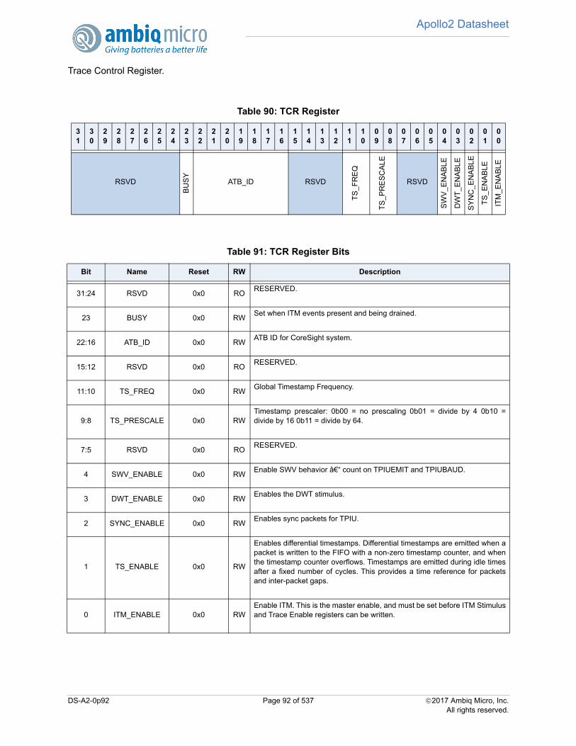
Apollo2 Datasheet
Trace Control Register.
Table 90: TCR Register
31
30
29
28
27
26
25
24
23
22
21
20
19
18
17
16
15
14
13
12
11
10
09
08
07
06
05
04
03
02
01
00
RSVDB
US
YATB_ID RSVD
TS
_F
RE
Q
TS
_PR
ES
CA
LE
RSVD
SW
V_E
NA
BLE
DW
T_E
NA
BLE
SY
NC
_EN
AB
LE
TS
_EN
AB
LE
ITM
_EN
AB
LE
Table 91: TCR Register Bits
Bit Name Reset RW Description
31:24 RSVD 0x0 RORESERVED.
23 BUSY 0x0 RWSet when ITM events present and being drained.
22:16 ATB_ID 0x0 RWATB ID for CoreSight system.
15:12 RSVD 0x0 RORESERVED.
11:10 TS_FREQ 0x0 RWGlobal Timestamp Frequency.
9:8 TS_PRESCALE 0x0 RWTimestamp prescaler: 0b00 = no prescaling 0b01 = divide by 4 0b10 =divide by 16 0b11 = divide by 64.
7:5 RSVD 0x0 RORESERVED.
4 SWV_ENABLE 0x0 RWEnable SWV behavior – count on TPIUEMIT and TPIUBAUD.
3 DWT_ENABLE 0x0 RWEnables the DWT stimulus.
2 SYNC_ENABLE 0x0 RWEnables sync packets for TPIU.
1 TS_ENABLE 0x0 RW
Enables differential timestamps. Differential timestamps are emitted when apacket is written to the FIFO with a non-zero timestamp counter, and whenthe timestamp counter overflows. Timestamps are emitted during idle timesafter a fixed number of cycles. This provides a time reference for packetsand inter-packet gaps.
0 ITM_ENABLE 0x0 RWEnable ITM. This is the master enable, and must be set before ITM Stimulusand Trace Enable registers can be written.
DS-A2-0p92 Page 92 of 537 2017 Ambiq Micro, Inc.All rights reserved.
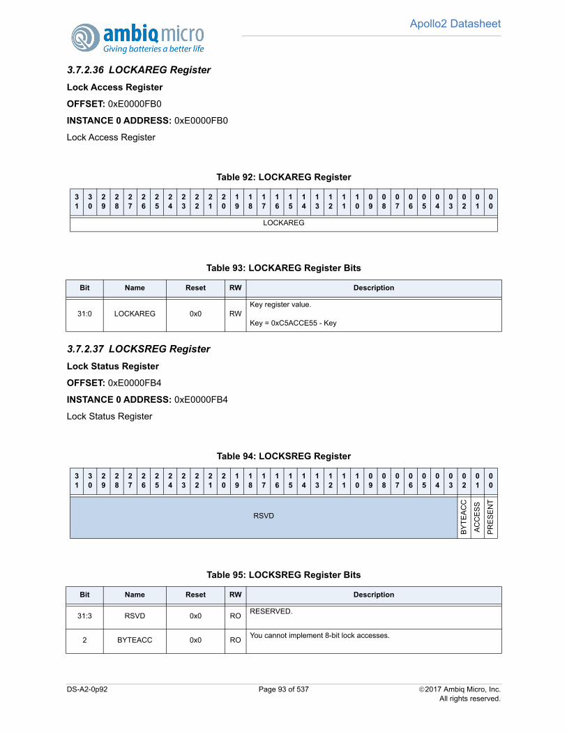
Apollo2 Datasheet
3.7.2.36 LOCKAREG Register
Lock Access Register
OFFSET: 0xE0000FB0
INSTANCE 0 ADDRESS: 0xE0000FB0
Lock Access Register
3.7.2.37 LOCKSREG Register
Lock Status Register
OFFSET: 0xE0000FB4
INSTANCE 0 ADDRESS: 0xE0000FB4
Lock Status Register
Table 92: LOCKAREG Register
31
30
29
28
27
26
25
24
23
22
21
20
19
18
17
16
15
14
13
12
11
10
09
08
07
06
05
04
03
02
01
00
LOCKAREG
Table 93: LOCKAREG Register Bits
Bit Name Reset RW Description
31:0 LOCKAREG 0x0 RWKey register value.
Key = 0xC5ACCE55 - Key
Table 94: LOCKSREG Register
31
30
29
28
27
26
25
24
23
22
21
20
19
18
17
16
15
14
13
12
11
10
09
08
07
06
05
04
03
02
01
00
RSVD
BY
TE
AC
C
AC
CE
SS
PR
ES
EN
T
Table 95: LOCKSREG Register Bits
Bit Name Reset RW Description
31:3 RSVD 0x0 RORESERVED.
2 BYTEACC 0x0 ROYou cannot implement 8-bit lock accesses.
DS-A2-0p92 Page 93 of 537 2017 Ambiq Micro, Inc.All rights reserved.

Apollo2 Datasheet
3.7.2.38 PID4 Register
Peripheral Identification Register 4
OFFSET: 0xE0000FD0
INSTANCE 0 ADDRESS: 0xE0000FD0
Peripheral Identification Register 4
3.7.2.39 PID5 Register
Peripheral Identification Register 5
OFFSET: 0xE0000FD4
INSTANCE 0 ADDRESS: 0xE0000FD4
Peripheral Identification Register 5
1 ACCESS 0x0 ROWrite access to component is blocked. All writes are ignored, reads are per-mitted.
0 PRESENT 0x1 ROIndicates that a lock mechanism exists for this component.
Table 96: PID4 Register
31
30
29
28
27
26
25
24
23
22
21
20
19
18
17
16
15
14
13
12
11
10
09
08
07
06
05
04
03
02
01
00
PID4
Table 97: PID4 Register Bits
Bit Name Reset RW Description
31:0 PID4 0x4 R0Peripheral Identification 4.
Table 98: PID5 Register
31
30
29
28
27
26
25
24
23
22
21
20
19
18
17
16
15
14
13
12
11
10
09
08
07
06
05
04
03
02
01
00
PID5
Table 95: LOCKSREG Register Bits
Bit Name Reset RW Description
DS-A2-0p92 Page 94 of 537 2017 Ambiq Micro, Inc.All rights reserved.
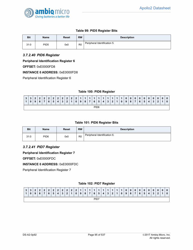
Apollo2 Datasheet
3.7.2.40 PID6 Register
Peripheral Identification Register 6
OFFSET: 0xE0000FD8
INSTANCE 0 ADDRESS: 0xE0000FD8
Peripheral Identification Register 6
3.7.2.41 PID7 Register
Peripheral Identification Register 7
OFFSET: 0xE0000FDC
INSTANCE 0 ADDRESS: 0xE0000FDC
Peripheral Identification Register 7
Table 99: PID5 Register Bits
Bit Name Reset RW Description
31:0 PID5 0x0 R0Peripheral Identification 5.
Table 100: PID6 Register
31
30
29
28
27
26
25
24
23
22
21
20
19
18
17
16
15
14
13
12
11
10
09
08
07
06
05
04
03
02
01
00
PID6
Table 101: PID6 Register Bits
Bit Name Reset RW Description
31:0 PID6 0x0 R0Peripheral Identification 6.
Table 102: PID7 Register
31
30
29
28
27
26
25
24
23
22
21
20
19
18
17
16
15
14
13
12
11
10
09
08
07
06
05
04
03
02
01
00
PID7
DS-A2-0p92 Page 95 of 537 2017 Ambiq Micro, Inc.All rights reserved.

Apollo2 Datasheet
3.7.2.42 PID0 Register
Peripheral Identification Register 0
OFFSET: 0xE0000FE0
INSTANCE 0 ADDRESS: 0xE0000FE0
Peripheral Identification Register 0
3.7.2.43 PID1 Register
Peripheral Identification Register 1
OFFSET: 0xE0000FE4
INSTANCE 0 ADDRESS: 0xE0000FE4
Peripheral Identification Register 1
Table 103: PID7 Register Bits
Bit Name Reset RW Description
31:0 PID7 0x0 R0Peripheral Identification 7.
Table 104: PID0 Register
31
30
29
28
27
26
25
24
23
22
21
20
19
18
17
16
15
14
13
12
11
10
09
08
07
06
05
04
03
02
01
00
PID0
Table 105: PID0 Register Bits
Bit Name Reset RW Description
31:0 PID0 0x1 R0Peripheral Identification 0.
Table 106: PID1 Register
31
30
29
28
27
26
25
24
23
22
21
20
19
18
17
16
15
14
13
12
11
10
09
08
07
06
05
04
03
02
01
00
PID1
DS-A2-0p92 Page 96 of 537 2017 Ambiq Micro, Inc.All rights reserved.

Apollo2 Datasheet
3.7.2.44 PID2 Register
Peripheral Identification Register 2
OFFSET: 0xE0000FE8
INSTANCE 0 ADDRESS: 0xE0000FE8
Peripheral Identification Register 2
3.7.2.45 PID3 Register
Peripheral Identification Register 3
OFFSET: 0xE0000FEC
INSTANCE 0 ADDRESS: 0xE0000FEC
Peripheral Identification Register 3
Table 107: PID1 Register Bits
Bit Name Reset RW Description
31:0 PID1 0xb0 R0Peripheral Identification 1.
Table 108: PID2 Register
31
30
29
28
27
26
25
24
23
22
21
20
19
18
17
16
15
14
13
12
11
10
09
08
07
06
05
04
03
02
01
00
PID2
Table 109: PID2 Register Bits
Bit Name Reset RW Description
31:0 PID2 0x3b R0Peripheral Identification 2.
Table 110: PID3 Register
31
30
29
28
27
26
25
24
23
22
21
20
19
18
17
16
15
14
13
12
11
10
09
08
07
06
05
04
03
02
01
00
PID3
DS-A2-0p92 Page 97 of 537 2017 Ambiq Micro, Inc.All rights reserved.
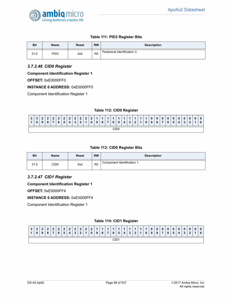
Apollo2 Datasheet
3.7.2.46 CID0 Register
Component Identification Register 1
OFFSET: 0xE0000FF0
INSTANCE 0 ADDRESS: 0xE0000FF0
Component Identification Register 1
3.7.2.47 CID1 Register
Component Identification Register 1
OFFSET: 0xE0000FF4
INSTANCE 0 ADDRESS: 0xE0000FF4
Component Identification Register 1
Table 111: PID3 Register Bits
Bit Name Reset RW Description
31:0 PID3 0x0 R0Peripheral Identification 3.
Table 112: CID0 Register
31
30
29
28
27
26
25
24
23
22
21
20
19
18
17
16
15
14
13
12
11
10
09
08
07
06
05
04
03
02
01
00
CID0
Table 113: CID0 Register Bits
Bit Name Reset RW Description
31:0 CID0 0xd R0Component Identification 1.
Table 114: CID1 Register
31
30
29
28
27
26
25
24
23
22
21
20
19
18
17
16
15
14
13
12
11
10
09
08
07
06
05
04
03
02
01
00
CID1
DS-A2-0p92 Page 98 of 537 2017 Ambiq Micro, Inc.All rights reserved.

Apollo2 Datasheet
3.7.2.48 CID2 Register
Component Identification Register 2
OFFSET: 0xE0000FF8
INSTANCE 0 ADDRESS: 0xE0000FF8
Component Identification Register 2
3.7.2.49 CID3 Register
Component Identification Register 3
OFFSET: 0xE0000FFC
INSTANCE 0 ADDRESS: 0xE0000FFC
Component Identification Register 3
Table 115: CID1 Register Bits
Bit Name Reset RW Description
31:0 CID1 0xe0 R0Component Identification 1.
Table 116: CID2 Register
31
30
29
28
27
26
25
24
23
22
21
20
19
18
17
16
15
14
13
12
11
10
09
08
07
06
05
04
03
02
01
00
CID2
Table 117: CID2 Register Bits
Bit Name Reset RW Description
31:0 CID2 0x5 R0Component Identification 2.
Table 118: CID3 Register
31
30
29
28
27
26
25
24
23
22
21
20
19
18
17
16
15
14
13
12
11
10
09
08
07
06
05
04
03
02
01
00
CID3
DS-A2-0p92 Page 99 of 537 2017 Ambiq Micro, Inc.All rights reserved.
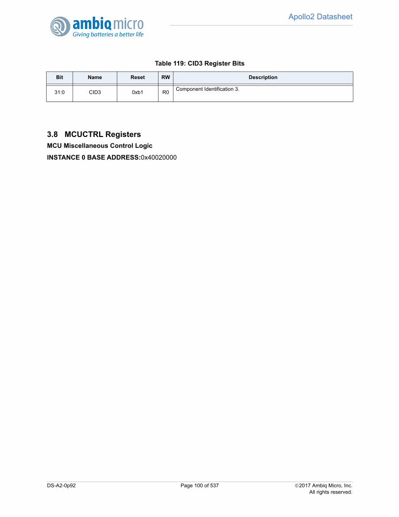
Apollo2 Datasheet
3.8 MCUCTRL RegistersMCU Miscellaneous Control Logic
INSTANCE 0 BASE ADDRESS:0x40020000
Table 119: CID3 Register Bits
Bit Name Reset RW Description
31:0 CID3 0xb1 R0Component Identification 3.
DS-A2-0p92 Page 100 of 537 2017 Ambiq Micro, Inc.All rights reserved.
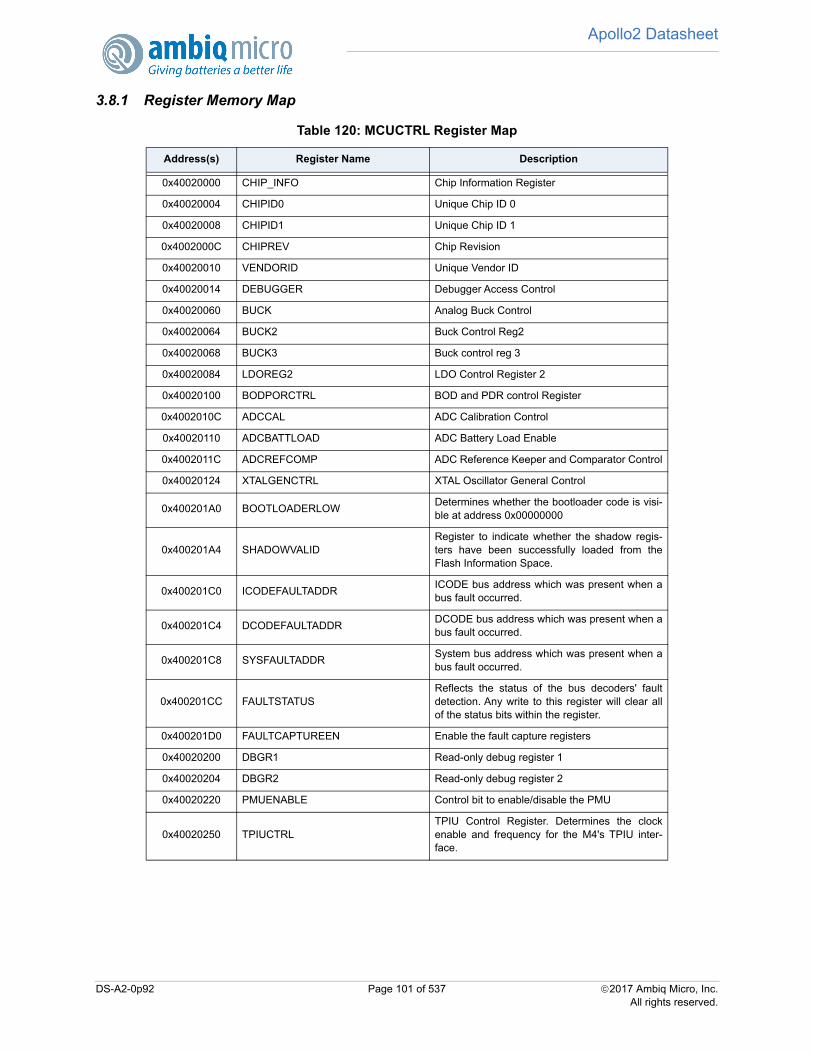
Apollo2 Datasheet
3.8.1 Register Memory Map
Table 120: MCUCTRL Register Map
Address(s) Register Name Description
0x40020000 CHIP_INFO Chip Information Register
0x40020004 CHIPID0 Unique Chip ID 0
0x40020008 CHIPID1 Unique Chip ID 1
0x4002000C CHIPREV Chip Revision
0x40020010 VENDORID Unique Vendor ID
0x40020014 DEBUGGER Debugger Access Control
0x40020060 BUCK Analog Buck Control
0x40020064 BUCK2 Buck Control Reg2
0x40020068 BUCK3 Buck control reg 3
0x40020084 LDOREG2 LDO Control Register 2
0x40020100 BODPORCTRL BOD and PDR control Register
0x4002010C ADCCAL ADC Calibration Control
0x40020110 ADCBATTLOAD ADC Battery Load Enable
0x4002011C ADCREFCOMP ADC Reference Keeper and Comparator Control
0x40020124 XTALGENCTRL XTAL Oscillator General Control
0x400201A0 BOOTLOADERLOWDetermines whether the bootloader code is visi-ble at address 0x00000000
0x400201A4 SHADOWVALIDRegister to indicate whether the shadow regis-ters have been successfully loaded from theFlash Information Space.
0x400201C0 ICODEFAULTADDRICODE bus address which was present when abus fault occurred.
0x400201C4 DCODEFAULTADDRDCODE bus address which was present when abus fault occurred.
0x400201C8 SYSFAULTADDRSystem bus address which was present when abus fault occurred.
0x400201CC FAULTSTATUSReflects the status of the bus decoders' faultdetection. Any write to this register will clear allof the status bits within the register.
0x400201D0 FAULTCAPTUREEN Enable the fault capture registers
0x40020200 DBGR1 Read-only debug register 1
0x40020204 DBGR2 Read-only debug register 2
0x40020220 PMUENABLE Control bit to enable/disable the PMU
0x40020250 TPIUCTRLTPIU Control Register. Determines the clockenable and frequency for the M4's TPIU inter-face.
DS-A2-0p92 Page 101 of 537 2017 Ambiq Micro, Inc.All rights reserved.

Apollo2 Datasheet
3.8.2 MCUCTRL Registers
3.8.2.1 CHIP_INFO Register
Chip Information Register
OFFSET: 0x00000000
INSTANCE 0 ADDRESS: 0x40020000
Chip Information Register
3.8.2.2 CHIPID0 Register
Unique Chip ID 0
OFFSET: 0x00000004
INSTANCE 0 ADDRESS: 0x40020004
Unique Chip ID 0
Table 121: CHIP_INFO Register
31
30
29
28
27
26
25
24
23
22
21
20
19
18
17
16
15
14
13
12
11
10
09
08
07
06
05
04
03
02
01
00
PARTNUM
Table 122: CHIP_INFO Register Bits
Bit Name Reset RW Description
31:0 PARTNUM 0x0 RO
BCD part number.
APOLLO2 = 0x3000000 - Apollo2 part number is 0x03XXXXXX.APOLLO = 0x1000000 - Apollo part number is 0x01XXXXXX.PN_M = 0xFF000000 - Mask for the PN field.
Table 123: CHIPID0 Register
31
30
29
28
27
26
25
24
23
22
21
20
19
18
17
16
15
14
13
12
11
10
09
08
07
06
05
04
03
02
01
00
VALUE
Table 124: CHIPID0 Register Bits
Bit Name Reset RW Description
31:0 VALUE 0x0 ROUnique chip ID 0.
APOLLO2 = 0x0 - Apollo2 CHIPID0 (see datasheet for details).
DS-A2-0p92 Page 102 of 537 2017 Ambiq Micro, Inc.All rights reserved.
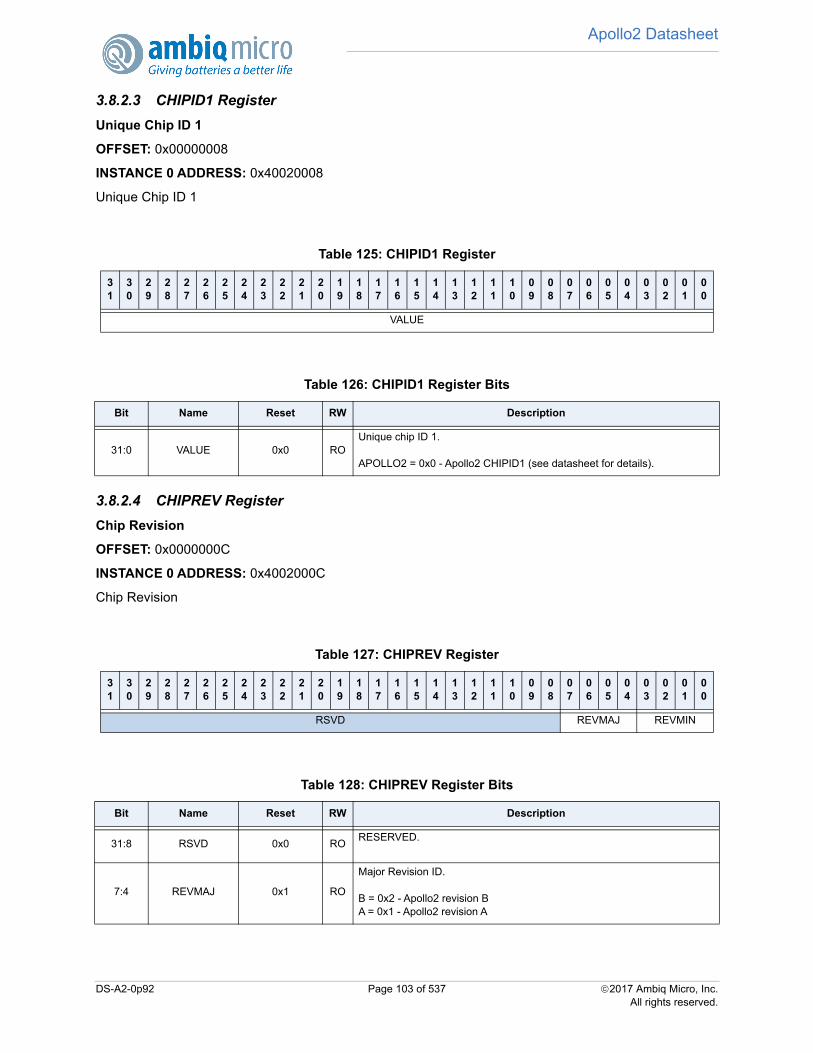
Apollo2 Datasheet
3.8.2.3 CHIPID1 Register
Unique Chip ID 1
OFFSET: 0x00000008
INSTANCE 0 ADDRESS: 0x40020008
Unique Chip ID 1
3.8.2.4 CHIPREV Register
Chip Revision
OFFSET: 0x0000000C
INSTANCE 0 ADDRESS: 0x4002000C
Chip Revision
Table 125: CHIPID1 Register
31
30
29
28
27
26
25
24
23
22
21
20
19
18
17
16
15
14
13
12
11
10
09
08
07
06
05
04
03
02
01
00
VALUE
Table 126: CHIPID1 Register Bits
Bit Name Reset RW Description
31:0 VALUE 0x0 ROUnique chip ID 1.
APOLLO2 = 0x0 - Apollo2 CHIPID1 (see datasheet for details).
Table 127: CHIPREV Register
31
30
29
28
27
26
25
24
23
22
21
20
19
18
17
16
15
14
13
12
11
10
09
08
07
06
05
04
03
02
01
00
RSVD REVMAJ REVMIN
Table 128: CHIPREV Register Bits
Bit Name Reset RW Description
31:8 RSVD 0x0 RORESERVED.
7:4 REVMAJ 0x1 RO
Major Revision ID.
B = 0x2 - Apollo2 revision BA = 0x1 - Apollo2 revision A
DS-A2-0p92 Page 103 of 537 2017 Ambiq Micro, Inc.All rights reserved.
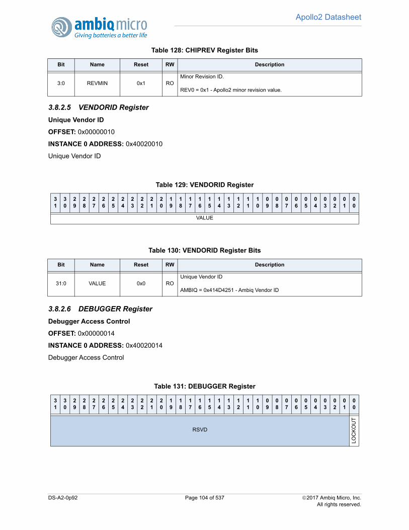
Apollo2 Datasheet
3.8.2.5 VENDORID Register
Unique Vendor ID
OFFSET: 0x00000010
INSTANCE 0 ADDRESS: 0x40020010
Unique Vendor ID
3.8.2.6 DEBUGGER Register
Debugger Access Control
OFFSET: 0x00000014
INSTANCE 0 ADDRESS: 0x40020014
Debugger Access Control
3:0 REVMIN 0x1 ROMinor Revision ID.
REV0 = 0x1 - Apollo2 minor revision value.
Table 129: VENDORID Register
31
30
29
28
27
26
25
24
23
22
21
20
19
18
17
16
15
14
13
12
11
10
09
08
07
06
05
04
03
02
01
00
VALUE
Table 130: VENDORID Register Bits
Bit Name Reset RW Description
31:0 VALUE 0x0 ROUnique Vendor ID
AMBIQ = 0x414D4251 - Ambiq Vendor ID
Table 131: DEBUGGER Register
31
30
29
28
27
26
25
24
23
22
21
20
19
18
17
16
15
14
13
12
11
10
09
08
07
06
05
04
03
02
01
00
RSVD
LOC
KO
UT
Table 128: CHIPREV Register Bits
Bit Name Reset RW Description
DS-A2-0p92 Page 104 of 537 2017 Ambiq Micro, Inc.All rights reserved.
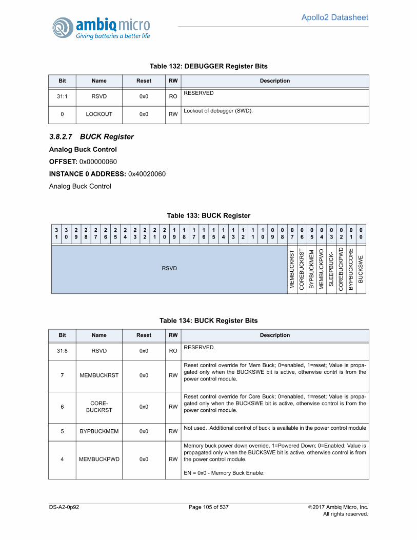
Apollo2 Datasheet
3.8.2.7 BUCK Register
Analog Buck Control
OFFSET: 0x00000060
INSTANCE 0 ADDRESS: 0x40020060
Analog Buck Control
Table 132: DEBUGGER Register Bits
Bit Name Reset RW Description
31:1 RSVD 0x0 RORESERVED
0 LOCKOUT 0x0 RWLockout of debugger (SWD).
Table 133: BUCK Register
31
30
29
28
27
26
25
24
23
22
21
20
19
18
17
16
15
14
13
12
11
10
09
08
07
06
05
04
03
02
01
00
RSVD
ME
MB
UC
KR
ST
CO
RE
BU
CK
RS
T
BY
PB
UC
KM
EM
ME
MB
UC
KP
WD
SL
EE
PB
UC
K-
CO
RE
BU
CK
PW
D
BY
PB
UC
KC
OR
E
BU
CK
SW
E
Table 134: BUCK Register Bits
Bit Name Reset RW Description
31:8 RSVD 0x0 RORESERVED.
7 MEMBUCKRST 0x0 RW
Reset control override for Mem Buck; 0=enabled, 1=reset; Value is propa-gated only when the BUCKSWE bit is active, otherwise contrl is from thepower control module.
6CORE-
BUCKRST0x0 RW
Reset control override for Core Buck; 0=enabled, 1=reset; Value is propa-gated only when the BUCKSWE bit is active, otherwise control is from thepower control module.
5 BYPBUCKMEM 0x0 RWNot used. Additional control of buck is available in the power control module
4 MEMBUCKPWD 0x0 RW
Memory buck power down override. 1=Powered Down; 0=Enabled; Value ispropagated only when the BUCKSWE bit is active, otherwise control is fromthe power control module.
EN = 0x0 - Memory Buck Enable.
DS-A2-0p92 Page 105 of 537 2017 Ambiq Micro, Inc.All rights reserved.
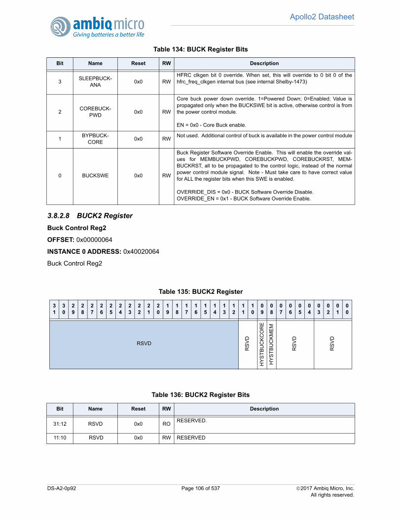
Apollo2 Datasheet
3.8.2.8 BUCK2 Register
Buck Control Reg2
OFFSET: 0x00000064
INSTANCE 0 ADDRESS: 0x40020064
Buck Control Reg2
3SLEEPBUCK-
ANA0x0 RW
HFRC clkgen bit 0 override. When set, this will override to 0 bit 0 of thehfrc_freq_clkgen internal bus (see internal Shelby-1473)
2COREBUCK-
PWD0x0 RW
Core buck power down override. 1=Powered Down; 0=Enabled; Value ispropagated only when the BUCKSWE bit is active, otherwise control is fromthe power control module.
EN = 0x0 - Core Buck enable.
1BYPBUCK-
CORE0x0 RW
Not used. Additional control of buck is available in the power control module
0 BUCKSWE 0x0 RW
Buck Register Software Override Enable. This will enable the override val-ues for MEMBUCKPWD, COREBUCKPWD, COREBUCKRST, MEM-BUCKRST, all to be propagated to the control logic, instead of the normalpower control module signal. Note - Must take care to have correct valuefor ALL the register bits when this SWE is enabled.
OVERRIDE_DIS = 0x0 - BUCK Software Override Disable.OVERRIDE_EN = 0x1 - BUCK Software Override Enable.
Table 135: BUCK2 Register
31
30
29
28
27
26
25
24
23
22
21
20
19
18
17
16
15
14
13
12
11
10
09
08
07
06
05
04
03
02
01
00
RSVD
RS
VD
HY
ST
BU
CK
CO
RE
HY
ST
BU
CK
ME
M
RS
VD
RS
VD
Table 136: BUCK2 Register Bits
Bit Name Reset RW Description
31:12 RSVD 0x0 RORESERVED.
11:10 RSVD 0x0 RW RESERVED
Table 134: BUCK Register Bits
Bit Name Reset RW Description
DS-A2-0p92 Page 106 of 537 2017 Ambiq Micro, Inc.All rights reserved.
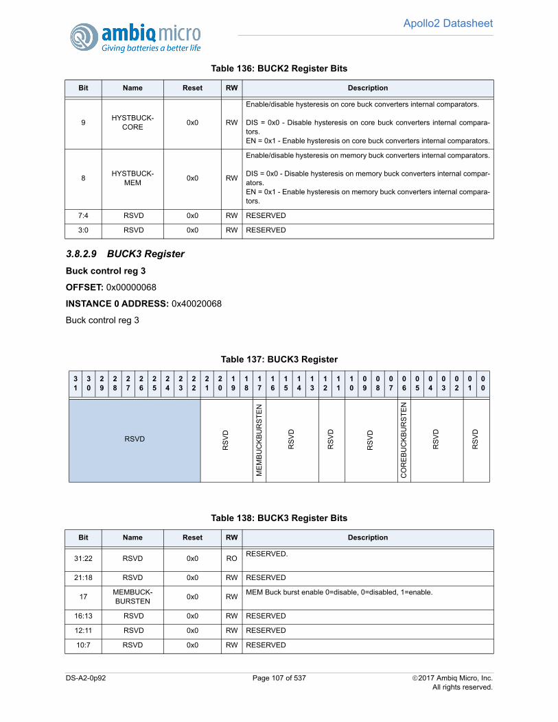
Apollo2 Datasheet
3.8.2.9 BUCK3 Register
Buck control reg 3
OFFSET: 0x00000068
INSTANCE 0 ADDRESS: 0x40020068
Buck control reg 3
9HYSTBUCK-
CORE0x0 RW
Enable/disable hysteresis on core buck converters internal comparators.
DIS = 0x0 - Disable hysteresis on core buck converters internal compara-tors.EN = 0x1 - Enable hysteresis on core buck converters internal comparators.
8HYSTBUCK-
MEM0x0 RW
Enable/disable hysteresis on memory buck converters internal comparators.
DIS = 0x0 - Disable hysteresis on memory buck converters internal compar-ators.EN = 0x1 - Enable hysteresis on memory buck converters internal compara-tors.
7:4 RSVD 0x0 RW RESERVED
3:0 RSVD 0x0 RW RESERVED
Table 137: BUCK3 Register
31
30
29
28
27
26
25
24
23
22
21
20
19
18
17
16
15
14
13
12
11
10
09
08
07
06
05
04
03
02
01
00
RSVD
RS
VD
ME
MB
UC
KB
UR
ST
EN
RS
VD
RS
VD
RS
VD
CO
RE
BU
CK
BU
RS
TE
N
RS
VD
RS
VD
Table 138: BUCK3 Register Bits
Bit Name Reset RW Description
31:22 RSVD 0x0 RORESERVED.
21:18 RSVD 0x0 RW RESERVED
17MEMBUCK-BURSTEN
0x0 RWMEM Buck burst enable 0=disable, 0=disabled, 1=enable.
16:13 RSVD 0x0 RW RESERVED
12:11 RSVD 0x0 RW RESERVED
10:7 RSVD 0x0 RW RESERVED
Table 136: BUCK2 Register Bits
Bit Name Reset RW Description
DS-A2-0p92 Page 107 of 537 2017 Ambiq Micro, Inc.All rights reserved.
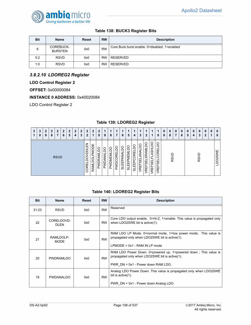
Apollo2 Datasheet
3.8.2.10 LDOREG2 Register
LDO Control Register 2
OFFSET: 0x00000084
INSTANCE 0 ADDRESS: 0x40020084
LDO Control Register 2
6COREBUCK-
BURSTEN0x0 RW
Core Buck burst enable. 0=disabled, 1=enabled
5:2 RSVD 0x0 RW RESERVED
1:0 RSVD 0x0 RW RESERVED
Table 139: LDOREG2 Register
31
30
29
28
27
26
25
24
23
22
21
20
19
18
17
16
15
14
13
12
11
10
09
08
07
06
05
04
03
02
01
00
RSVD
CO
RE
LDO
VD
DLE
N
RA
MLD
OLP
MO
DE
PW
DR
AM
LDO
PW
DA
NA
LDO
PW
DM
EM
LD
O
PW
DC
OR
ELD
O
SLE
EP
AN
ALD
O
SLE
EP
ME
MLD
O
SLE
EP
CO
RE
LDO
VR
EF
SE
LAN
ALD
O
VR
EF
SE
LSR
AM
LDO
VR
EF
SE
LF
LAS
HLD
O
VR
EF
SE
LCO
RE
LDO
RS
VD
RS
VD
LDO
2SW
E
Table 140: LDOREG2 Register Bits
Bit Name Reset RW Description
31:23 RSVD 0x0 RWReserved
22CORELDOVD-
DLEN0x0 RW
Core LDO output enable. 0=Hi-Z, 1=enable. This value is propagated onlywhen LDO2SWE bit is active(1).
21RAMLDOLP-
MODE0x0 RW
RAM LDO LP Mode. 0=normal mode, 1=low power mode; This value ispropagated only when LDO2SWE bit is active(1).
LPMODE = 0x1 - RAM IN LP mode
20 PWDRAMLDO 0x0 RW
RAM LDO Power Down. 0=powered up, 1=powered down ; This value ispropagated only when LDO2SWE bit is active(1).
PWR_DN = 0x1 - Power down RAM LDO.
19 PWDANALDO 0x0 RW
Analog LDO Power Down. This value is propagated only when LDO2SWEbit is active(1).
PWR_DN = 0x1 - Power down Analog LDO.
Table 138: BUCK3 Register Bits
Bit Name Reset RW Description
DS-A2-0p92 Page 108 of 537 2017 Ambiq Micro, Inc.All rights reserved.

Apollo2 Datasheet
3.8.2.11 BODPORCTRL Register
BOD and PDR control Register
OFFSET: 0x00000100
INSTANCE 0 ADDRESS: 0x40020100
BOD and PDR control Register
18 PWDMEMLDO 0x0 RW
MEM LDO Power Down. This value is propagated only when LDO2SWE bitis active(1).
PWR_DN = 0x1 - Power down Flash LDO.
17 PWDCORELDO 0x0 RW
CORE LDO Power Down. This value is propagated only when LDO2SWEbit is active(1).
PWR_DN = 0x1 - Power down Core LDO.
16 SLEEPANALDO 0x0 RW
Analog LDO Sleep. This value is propagated only when LDO2SWE bit isactive(1).
SLEEP = 0x1 - Analog LDO sleep.
15SLEEPMEM-
LDO0x0 RW
FLASH LDO Sleep. This value is propagated only when LDO2SWE bit isactive(1).
SLEEP = 0x1 - SRAM LDO sleep.
14SLEEP-
CORELDO0x0 RW
CORE LDO Sleep. This value is propagated only when LDO2SWE bit isactive(1).
SLEEP = 0x1 - Core LDO sleep.
13VREFSELA-
NALDO0x0 RW
CONTROL BIT IS NOT USED. PLEASE TREAT AS RESERVED
12VREFSEL-SRAMLDO
0x0 RWCONTROL BIT IS NOT USED. PLEASE TREAT AS RESERVED
11VREF-
SELFLASHLDO0x0 RW
CONTROL BIT IS NOT USED. PLEASE TREAT AS RESERVED
10VREFSEL-CORELDO
0x0 RWCONTROL BIT IS NOT USED. PLEASE TREAT AS RESERVED
9:6 RSVD 0x0 RW RESERVED
5:1 RSVD 0x0 RW RESERVED
0 LDO2SWE 0x0 RW
LDO2 Software Override Enable. If enabled (=1), this will enable the over-ride values from this register to be used instead of the normal control signalsfor the following fields: CORELDOVDDLEN, RAMLDOLPMODE,PWDRAMLDO, PWDANALDO, PWDMEMLDO, PWDCORELDO, SLEEP-ANALDO, SLEEPMEMLDO, SLEEPCORELDO.
OVERRIDE_DIS = 0x0 - LDO2 Software Override Disable.OVERRIDE_EN = 0x1 - LDO2 Software Override Enable.
Table 140: LDOREG2 Register Bits
Bit Name Reset RW Description
DS-A2-0p92 Page 109 of 537 2017 Ambiq Micro, Inc.All rights reserved.
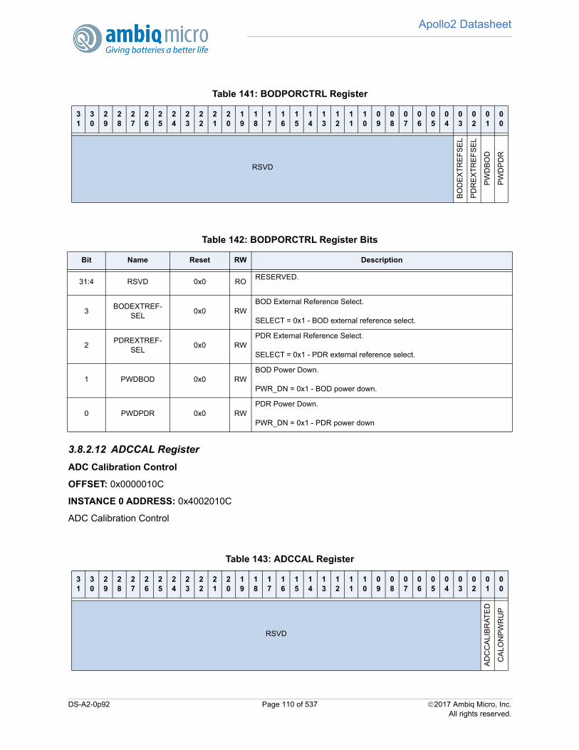
Apollo2 Datasheet
3.8.2.12 ADCCAL Register
ADC Calibration Control
OFFSET: 0x0000010C
INSTANCE 0 ADDRESS: 0x4002010C
ADC Calibration Control
Table 141: BODPORCTRL Register
31
30
29
28
27
26
25
24
23
22
21
20
19
18
17
16
15
14
13
12
11
10
09
08
07
06
05
04
03
02
01
00
RSVD
BO
DE
XT
RE
FS
EL
PD
RE
XT
RE
FS
EL
PW
DB
OD
PW
DP
DR
Table 142: BODPORCTRL Register Bits
Bit Name Reset RW Description
31:4 RSVD 0x0 RORESERVED.
3BODEXTREF-
SEL0x0 RW
BOD External Reference Select.
SELECT = 0x1 - BOD external reference select.
2PDREXTREF-
SEL0x0 RW
PDR External Reference Select.
SELECT = 0x1 - PDR external reference select.
1 PWDBOD 0x0 RWBOD Power Down.
PWR_DN = 0x1 - BOD power down.
0 PWDPDR 0x0 RWPDR Power Down.
PWR_DN = 0x1 - PDR power down
Table 143: ADCCAL Register
31
30
29
28
27
26
25
24
23
22
21
20
19
18
17
16
15
14
13
12
11
10
09
08
07
06
05
04
03
02
01
00
RSVD
AD
CC
ALI
BR
AT
ED
CA
LON
PW
RU
P
DS-A2-0p92 Page 110 of 537 2017 Ambiq Micro, Inc.All rights reserved.

Apollo2 Datasheet
3.8.2.13 ADCBATTLOAD Register
ADC Battery Load Enable
OFFSET: 0x00000110
INSTANCE 0 ADDRESS: 0x40020110
ADC Battery Load Enable
3.8.2.14 ADCREFCOMP Register
ADC Reference Keeper and Comparator Control
OFFSET: 0x0000011C
INSTANCE 0 ADDRESS: 0x4002011C
ADC Reference Keeper and Comparator Control
Table 144: ADCCAL Register Bits
Bit Name Reset RW Description
31:2 RSVD 0x0 RORESERVED.
1ADCCALI-BRATED
0x0 RO
Status for ADC Calibration
FALSE = 0x0 - ADC is not calibratedTRUE = 0x1 - ADC is calibrated
0 CALONPWRUP 0x1 RW
Run ADC Calibration on initial power up sequence
DIS = 0x0 - Disable automatic calibration on initial power upEN = 0x1 - Enable automatic calibration on initial power up
Table 145: ADCBATTLOAD Register
31
30
29
28
27
26
25
24
23
22
21
20
19
18
17
16
15
14
13
12
11
10
09
08
07
06
05
04
03
02
01
00
RSVD
BA
TT
LO
AD
Table 146: ADCBATTLOAD Register Bits
Bit Name Reset RW Description
31:1 RSVD 0x0 RORESERVED.
0 BATTLOAD 0x0 RW
Enable the ADC battery load resistor
DIS = 0x0 - Battery load is disconnectedEN = 0x1 - Battery load is enabled
DS-A2-0p92 Page 111 of 537 2017 Ambiq Micro, Inc.All rights reserved.
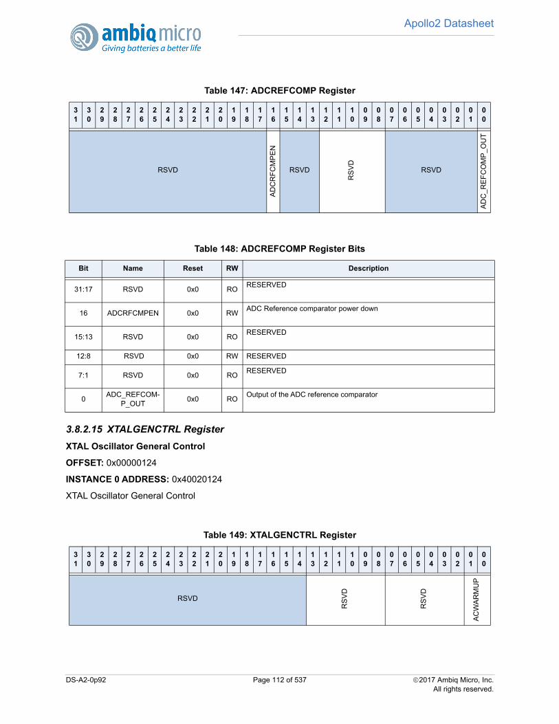
Apollo2 Datasheet
3.8.2.15 XTALGENCTRL Register
XTAL Oscillator General Control
OFFSET: 0x00000124
INSTANCE 0 ADDRESS: 0x40020124
XTAL Oscillator General Control
Table 147: ADCREFCOMP Register
31
30
29
28
27
26
25
24
23
22
21
20
19
18
17
16
15
14
13
12
11
10
09
08
07
06
05
04
03
02
01
00
RSVD
AD
CR
FC
MP
EN
RSVD
RS
VD
RSVD
AD
C_R
EF
CO
MP
_OU
T
Table 148: ADCREFCOMP Register Bits
Bit Name Reset RW Description
31:17 RSVD 0x0 RORESERVED
16 ADCRFCMPEN 0x0 RWADC Reference comparator power down
15:13 RSVD 0x0 RORESERVED
12:8 RSVD 0x0 RW RESERVED
7:1 RSVD 0x0 RORESERVED
0ADC_REFCOM-
P_OUT0x0 RO
Output of the ADC reference comparator
Table 149: XTALGENCTRL Register
31
30
29
28
27
26
25
24
23
22
21
20
19
18
17
16
15
14
13
12
11
10
09
08
07
06
05
04
03
02
01
00
RSVD
RS
VD
RS
VD
AC
WA
RM
UP
DS-A2-0p92 Page 112 of 537 2017 Ambiq Micro, Inc.All rights reserved.
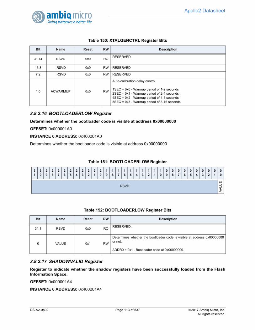
Apollo2 Datasheet
3.8.2.16 BOOTLOADERLOW Register
Determines whether the bootloader code is visible at address 0x00000000
OFFSET: 0x000001A0
INSTANCE 0 ADDRESS: 0x400201A0
Determines whether the bootloader code is visible at address 0x00000000
3.8.2.17 SHADOWVALID Register
Register to indicate whether the shadow registers have been successfully loaded from the FlashInformation Space.
OFFSET: 0x000001A4
INSTANCE 0 ADDRESS: 0x400201A4
Table 150: XTALGENCTRL Register Bits
Bit Name Reset RW Description
31:14 RSVD 0x0 RORESERVED.
13:8 RSVD 0x0 RW RESERVED
7:2 RSVD 0x0 RW RESERVED
1:0 ACWARMUP 0x0 RW
Auto-calibration delay control
1SEC = 0x0 - Warmup period of 1-2 seconds2SEC = 0x1 - Warmup period of 2-4 seconds4SEC = 0x2 - Warmup period of 4-8 seconds8SEC = 0x3 - Warmup period of 8-16 seconds
Table 151: BOOTLOADERLOW Register
31
30
29
28
27
26
25
24
23
22
21
20
19
18
17
16
15
14
13
12
11
10
09
08
07
06
05
04
03
02
01
00
RSVD
VA
LUE
Table 152: BOOTLOADERLOW Register Bits
Bit Name Reset RW Description
31:1 RSVD 0x0 RORESERVED.
0 VALUE 0x1 RW
Determines whether the bootloader code is visible at address 0x00000000or not.
ADDR0 = 0x1 - Bootloader code at 0x00000000.
DS-A2-0p92 Page 113 of 537 2017 Ambiq Micro, Inc.All rights reserved.

Apollo2 Datasheet
Register to indicate whether the shadow registers have been successfully loaded from the FlashInformation Space.
3.8.2.18 ICODEFAULTADDR Register
ICODE bus address which was present when a bus fault occurred.
OFFSET: 0x000001C0
INSTANCE 0 ADDRESS: 0x400201C0
ICODE bus address which was present when a bus fault occurred.
Table 153: SHADOWVALID Register
31
30
29
28
27
26
25
24
23
22
21
20
19
18
17
16
15
14
13
12
11
10
09
08
07
06
05
04
03
02
01
00
RSVD
BL_
DS
LEE
P
VA
LID
Table 154: SHADOWVALID Register Bits
Bit Name Reset RW Description
31:2 RSVD 0x0 RORESERVED.
1 BL_DSLEEP 0x1 RO
Indicates whether the bootloader should sleep or deep sleep if no imageloaded.
DEEPSLEEP = 0x1 - Bootloader will go to deep sleep if no flash imageloaded
0 VALID 0x1 RO
Indicates whether the shadow registers contain valid data from the FlashInformation Space.
VALID = 0x1 - Flash information space contains valid data.
Table 155: ICODEFAULTADDR Register
31
30
29
28
27
26
25
24
23
22
21
20
19
18
17
16
15
14
13
12
11
10
09
08
07
06
05
04
03
02
01
00
ADDR
DS-A2-0p92 Page 114 of 537 2017 Ambiq Micro, Inc.All rights reserved.
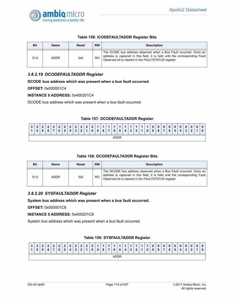
Apollo2 Datasheet
3.8.2.19 DCODEFAULTADDR Register
DCODE bus address which was present when a bus fault occurred.
OFFSET: 0x000001C4
INSTANCE 0 ADDRESS: 0x400201C4
DCODE bus address which was present when a bus fault occurred.
3.8.2.20 SYSFAULTADDR Register
System bus address which was present when a bus fault occurred.
OFFSET: 0x000001C8
INSTANCE 0 ADDRESS: 0x400201C8
System bus address which was present when a bus fault occurred.
Table 156: ICODEFAULTADDR Register Bits
Bit Name Reset RW Description
31:0 ADDR 0x0 RO
The ICODE bus address observed when a Bus Fault occurred. Once anaddress is captured in this field, it is held until the corresponding FaultObserved bit is cleared in the FAULTSTATUS register.
Table 157: DCODEFAULTADDR Register
31
30
29
28
27
26
25
24
23
22
21
20
19
18
17
16
15
14
13
12
11
10
09
08
07
06
05
04
03
02
01
00
ADDR
Table 158: DCODEFAULTADDR Register Bits
Bit Name Reset RW Description
31:0 ADDR 0x0 RO
The DCODE bus address observed when a Bus Fault occurred. Once anaddress is captured in this field, it is held until the corresponding FaultObserved bit is cleared in the FAULTSTATUS register.
Table 159: SYSFAULTADDR Register
31
30
29
28
27
26
25
24
23
22
21
20
19
18
17
16
15
14
13
12
11
10
09
08
07
06
05
04
03
02
01
00
ADDR
DS-A2-0p92 Page 115 of 537 2017 Ambiq Micro, Inc.All rights reserved.
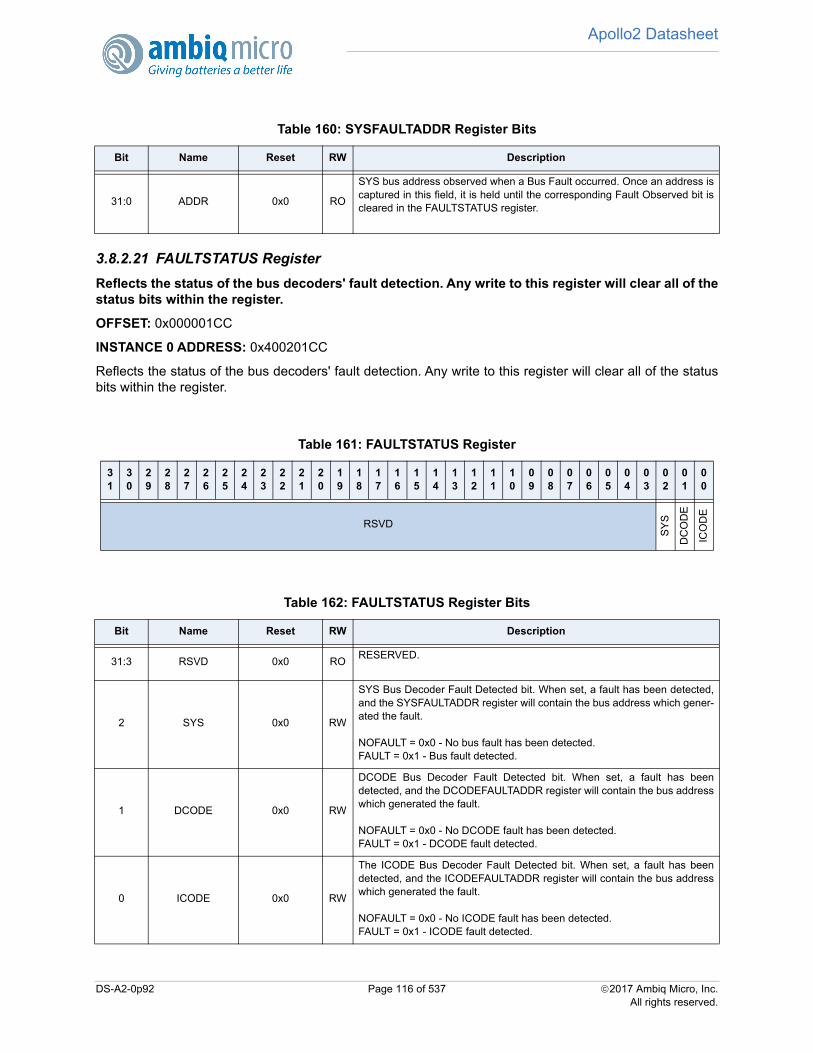
Apollo2 Datasheet
3.8.2.21 FAULTSTATUS Register
Reflects the status of the bus decoders' fault detection. Any write to this register will clear all of thestatus bits within the register.
OFFSET: 0x000001CC
INSTANCE 0 ADDRESS: 0x400201CC
Reflects the status of the bus decoders' fault detection. Any write to this register will clear all of the statusbits within the register.
Table 160: SYSFAULTADDR Register Bits
Bit Name Reset RW Description
31:0 ADDR 0x0 RO
SYS bus address observed when a Bus Fault occurred. Once an address iscaptured in this field, it is held until the corresponding Fault Observed bit iscleared in the FAULTSTATUS register.
Table 161: FAULTSTATUS Register
31
30
29
28
27
26
25
24
23
22
21
20
19
18
17
16
15
14
13
12
11
10
09
08
07
06
05
04
03
02
01
00
RSVD
SY
S
DC
OD
E
ICO
DE
Table 162: FAULTSTATUS Register Bits
Bit Name Reset RW Description
31:3 RSVD 0x0 RORESERVED.
2 SYS 0x0 RW
SYS Bus Decoder Fault Detected bit. When set, a fault has been detected,and the SYSFAULTADDR register will contain the bus address which gener-ated the fault.
NOFAULT = 0x0 - No bus fault has been detected.FAULT = 0x1 - Bus fault detected.
1 DCODE 0x0 RW
DCODE Bus Decoder Fault Detected bit. When set, a fault has beendetected, and the DCODEFAULTADDR register will contain the bus addresswhich generated the fault.
NOFAULT = 0x0 - No DCODE fault has been detected.FAULT = 0x1 - DCODE fault detected.
0 ICODE 0x0 RW
The ICODE Bus Decoder Fault Detected bit. When set, a fault has beendetected, and the ICODEFAULTADDR register will contain the bus addresswhich generated the fault.
NOFAULT = 0x0 - No ICODE fault has been detected.FAULT = 0x1 - ICODE fault detected.
DS-A2-0p92 Page 116 of 537 2017 Ambiq Micro, Inc.All rights reserved.
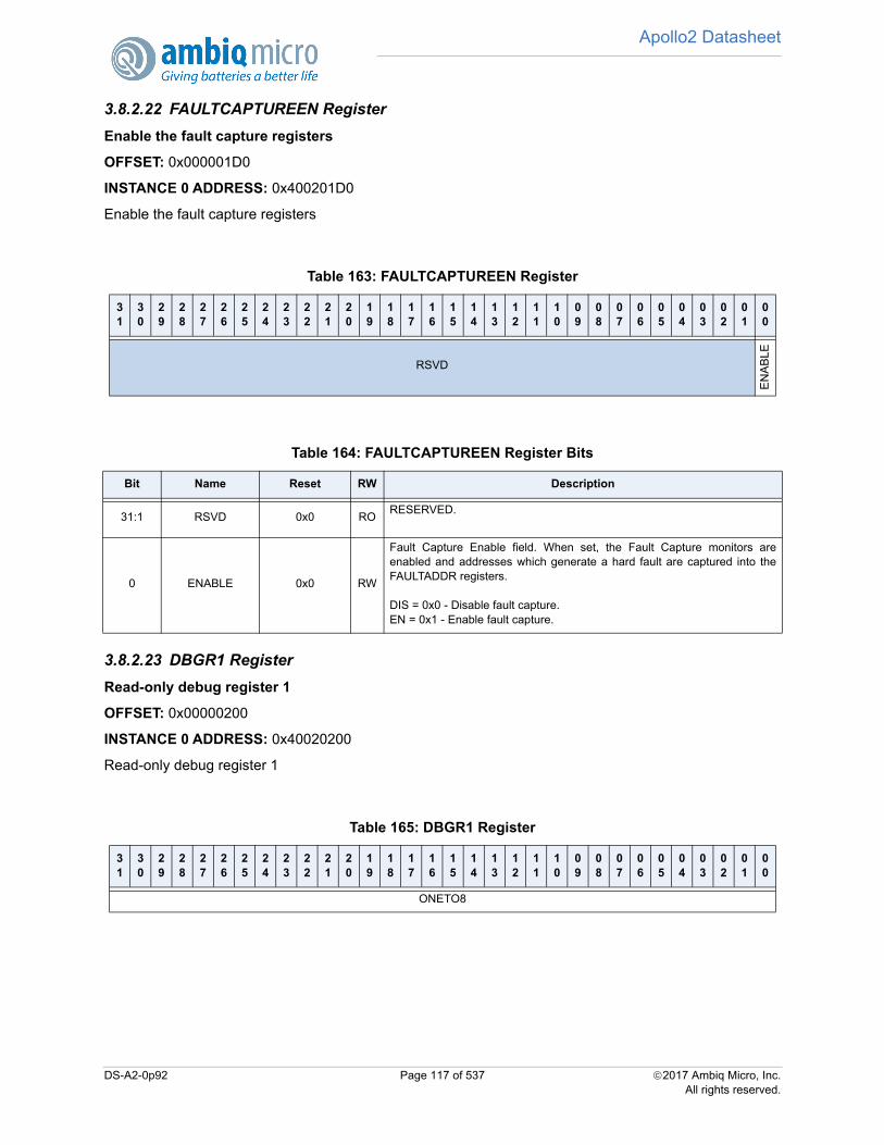
Apollo2 Datasheet
3.8.2.22 FAULTCAPTUREEN Register
Enable the fault capture registers
OFFSET: 0x000001D0
INSTANCE 0 ADDRESS: 0x400201D0
Enable the fault capture registers
3.8.2.23 DBGR1 Register
Read-only debug register 1
OFFSET: 0x00000200
INSTANCE 0 ADDRESS: 0x40020200
Read-only debug register 1
Table 163: FAULTCAPTUREEN Register
31
30
29
28
27
26
25
24
23
22
21
20
19
18
17
16
15
14
13
12
11
10
09
08
07
06
05
04
03
02
01
00
RSVD
EN
AB
LE
Table 164: FAULTCAPTUREEN Register Bits
Bit Name Reset RW Description
31:1 RSVD 0x0 RORESERVED.
0 ENABLE 0x0 RW
Fault Capture Enable field. When set, the Fault Capture monitors areenabled and addresses which generate a hard fault are captured into theFAULTADDR registers.
DIS = 0x0 - Disable fault capture.EN = 0x1 - Enable fault capture.
Table 165: DBGR1 Register
31
30
29
28
27
26
25
24
23
22
21
20
19
18
17
16
15
14
13
12
11
10
09
08
07
06
05
04
03
02
01
00
ONETO8
DS-A2-0p92 Page 117 of 537 2017 Ambiq Micro, Inc.All rights reserved.
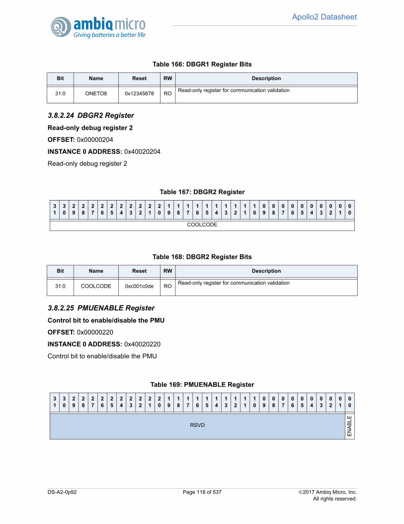
Apollo2 Datasheet
3.8.2.24 DBGR2 Register
Read-only debug register 2
OFFSET: 0x00000204
INSTANCE 0 ADDRESS: 0x40020204
Read-only debug register 2
3.8.2.25 PMUENABLE Register
Control bit to enable/disable the PMU
OFFSET: 0x00000220
INSTANCE 0 ADDRESS: 0x40020220
Control bit to enable/disable the PMU
Table 166: DBGR1 Register Bits
Bit Name Reset RW Description
31:0 ONETO8 0x12345678 RORead-only register for communication validation
Table 167: DBGR2 Register
31
30
29
28
27
26
25
24
23
22
21
20
19
18
17
16
15
14
13
12
11
10
09
08
07
06
05
04
03
02
01
00
COOLCODE
Table 168: DBGR2 Register Bits
Bit Name Reset RW Description
31:0 COOLCODE 0xc001c0de RORead-only register for communication validation
Table 169: PMUENABLE Register
31
30
29
28
27
26
25
24
23
22
21
20
19
18
17
16
15
14
13
12
11
10
09
08
07
06
05
04
03
02
01
00
RSVD
EN
AB
LE
DS-A2-0p92 Page 118 of 537 2017 Ambiq Micro, Inc.All rights reserved.
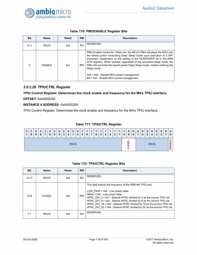
Apollo2 Datasheet
3.8.2.26 TPIUCTRL Register
TPIU Control Register. Determines the clock enable and frequency for the M4's TPIU interface.
OFFSET: 0x00000250
INSTANCE 0 ADDRESS: 0x40020250
TPIU Control Register. Determines the clock enable and frequency for the M4's TPIU interface.
Table 170: PMUENABLE Register Bits
Bit Name Reset RW Description
31:1 RSVD 0x0 RORESERVED.
0 ENABLE 0x1 RW
PMU Enable Control bit. When set, the MCU's PMU will place the MCU intothe lowest power consuming Deep Sleep mode upon execution of a WFIinstruction (dependent on the setting of the SLEEPDEEP bit in the ARMSCR register). When cleared, regardless of the requested sleep mode, thePMU will not enter the lowest power Deep Sleep mode, instead entering theSleep mode.
DIS = 0x0 - Disable MCU power management.EN = 0x1 - Enable MCU power management.
Table 171: TPIUCTRL Register
31
30
29
28
27
26
25
24
23
22
21
20
19
18
17
16
15
14
13
12
11
10
09
08
07
06
05
04
03
02
01
00
RSVD
CLK
SE
L
RSVD
EN
AB
LE
Table 172: TPIUCTRL Register Bits
Bit Name Reset RW Description
31:11 RSVD 0x0 RORESERVED.
10:8 CLKSEL 0x0 RW
This field selects the frequency of the ARM M4 TPIU port.
LOW_PWR = 0x0 - Low power state.0MHz = 0x0 - Low power state.HFRC_DIV_2 = 0x1 - Selects HFRC divided by 2 as the source TPIU clkHFRC_DIV_8 = 0x2 - Selects HFRC divided by 8 as the source TPIU clkHFRC_DIV_16 = 0x3 - Selects HFRC divided by 16 as the source TPIU clkHFRC_DIV_32 = 0x4 - Selects HFRC divided by 32 as the source TPIU clk
7:1 RSVD 0x0 RORESERVED.
DS-A2-0p92 Page 119 of 537 2017 Ambiq Micro, Inc.All rights reserved.
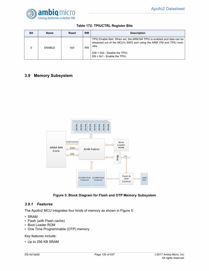
Apollo2 Datasheet
3.9 Memory Subsystem
Figure 5. Block Diagram for Flash and OTP Memory Subsystem
3.9.1 Features
The Apollo2 MCU integrates four kinds of memory as shown in Figure 5:
SRAM Flash (with Flash cache) Boot Loader ROM One Time Programmable (OTP) memory
Key features include:
Up to 256 KB SRAM
0 ENABLE 0x0 RW
TPIU Enable field. When set, the ARM M4 TPIU is enabled and data can bestreamed out of the MCU's SWO port using the ARM ITM and TPIU mod-ules.
DIS = 0x0 - Disable the TPIU.EN = 0x1 - Enable the TPIU.
Table 172: TPIUCTRL Register Bits
Bit Name Reset RW Description
ARM M4 Core AHB Fabric
Instruction
Data
SYS
8KB S
RAM
8KB S
RAM
8KB S
RAM
8KB S
RAM
8KB S
RAM
8KB S
RAM
8KB S
RAM
8KB S
RAM
8KB S
RAM
8KB S
RAM
8KB S
RAM
8KB S
RAM
8KB S
RAM
8KB S
RAM
8KB S
RAM
8KB S
RAM
8KB S
RAM
8KB S
RAM
8KB S
RAM
8KB S
RAM
8KB S
RAM
8KB S
RAM
8KB S
RAM
8KB S
RAM
8KB S
RAM
8KB S
RAM
8KB S
RAM
8KB S
RAM
8KB S
RAM
8KB S
RAM
8KB S
RAM
8KB S
RAM
Boot Loader ROM
Bridg
e
512KB Flash Instance
512KB Flash Instance
APB
Flash & OTP
Control
16KB OTP
DS-A2-0p92 Page 120 of 537 2017 Ambiq Micro, Inc.All rights reserved.

Apollo2 Datasheet
Up to 2 Instances of 512 KB flash Memory (up to 1 MB total) 16 KB Flash cache (2-way set-associative, 512 entry, 128b linesize) 16KBytes OTP
- 8KBytes contain factory preset per chip trim values.- 8KBytes for customer use, including flash protection fields
Flash Protection specified in 16 KB Chunks- 64 OTP bits specify Write Protected Chunks- 64 OTP bits specify Read Protected Chunks- A Chunk is Execute Only if Both Corresponding Protection Bits Specified- OTP bits Specify Debugger Lock Out State- OTP bits Can Protect SRAM Contents From Debugger Inspection
3.9.2 Functional Overview
The Apollo2 MCU Integrates up to 1024 KBytes of on-board flash memory and 16 Kbytes of one timeprogrammable memory. These two memories are managed by the APB flash controller for writeoperations.
During normal MCU code execution, the Flash Cache Controller translates requests from the CPU core tothe Flash Memory instance for instruction and data fetches. The Controller is designed to return data inzero wait-states when accesses hit into the cache and can operate up to the maximum operatingfrequency of the CPU core. On cache misses, the controller issues miss requests to the Flash memorycontroller.
The Flash Memory Controller facilitates flash erase and programming operations. When erase orprogramming operations are active, instructions cannot be fetched for execution from the Flash memory,so the on-chip SRAM would have to be used for code execution. The cache controller ensures theseoperations are synchronized. To facilitate the management of flash updates and OTP programming, anumber of flash helper functions are provided in the boot loader ROM.
The boot loader ROM contains approximately 2 KB of instructions that are executed upon power up of theprocessor. Once a valid reset vector is establish at offset zero in the flash memory, the boot loadertransfers control to users application by issuing a POR type reset which causes the core to enter the resetvector in flash. This process occupies less than 100 instructions in the boot loader. The remainder of theboot loader is occupied by a set of flash helper functions.
DS-A2-0p92 Page 121 of 537 2017 Ambiq Micro, Inc.All rights reserved.
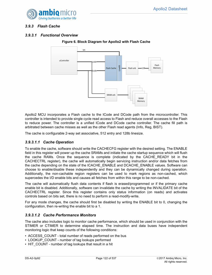
Apollo2 Datasheet
3.9.3 Flash Cache
3.9.3.1 Functional Overview
Figure 6. Block Diagram for Apollo2 with Flash Cache
Apollo2 MCU incorporates a Flash cache to the ICode and DCode path from the microcontroller. Thiscontroller is intended to provide single cycle read access to Flash and reduce overall accesses to the Flashto reduce power. The controller is a unified ICode and DCode cache controller. The cache fill path isarbitrated between cache misses as well as the other Flash read agents (Info, Reg, BIST).
The cache is configurable 2-way set associative, 512 entry and 128b linesize.
3.9.3.1.1 Cache Operation
To enable the cache, software should write the CACHECFG register with the desired setting. The ENABLEfield in this register will power up the cache SRAMs and initiate the cache startup sequence which will flushthe cache RAMs. Once the sequence is complete (indicated by the CACHE_READY bit in theCACHECTRL register), the cache will automatically begin servicing instruction and/or data fetches fromthe cache depending on the state of the ICACHE_ENABLE and DCACHE_ENABLE values. Software canchoose to enable/disable these independently and they can be dynamically changed during operation.Additionally, the non-cachable region registers can be used to mark regions as non-cached, whichsupercedes the I/D enable bits and causes all fetches from within this range to be non-cached.
The cache will automatically flush data contents if flash is erased/programmed or if the primary cacheenable bit is disabled. Additionally, software can invalidate the cache by writing the INVALIDATE bit of theCACHECTRL register. Since this register contains only status information (on reads) and activatescontrols based on bits set, there is no need to perform a read-modify-write.
For any mode changes, the cache should first be disabled by writing the ENABLE bit to 0, changing theconfiguration, then re-writing the enable bit to a 1.
3.9.3.1.2 Cache Performance Monitors
The cache also includes logic to monitor cache performance, which should be used in conjunction with theSTIMER or CTIMER to determine elapsed time. The instruction and data buses have independentmonitoring logic that keep counts of the following conditions:
ACCESS_COUNT - total number of reads performed on the bus LOOKUP_COUNT - number of tag lookups performed HIT_COUNT - number of tag lookups that result in a hit
uController
dcode
icode
Flash Cache
Flash MemoryFlash
Memory
Line
fill
128
SRAM arb
SRAM MemorySRAM
MemorySRAM MemorySRAM
Memory
Flash arb
sys
DS-A2-0p92 Page 122 of 537 2017 Ambiq Micro, Inc.All rights reserved.
Apollo2 Datasheet
LINE_COUNT - number of reads that were serviced from the line buffers (on a miss or non-cached access) or directly from the RAM because they fell within the same line as the previous lookup.
The LOOKUP and LINE counts should sum to the ACCESS COUNT and the number of cache misses canbe calculated as LOOKUP_COUNT - HIT_COUNT.
Cache monitors will automatically freeze the counts when either of the access counters reaches a value of0xFFFF0000 to prevent the counters from rolling over. The monitor counts can be reset at any time bywriting the RESET_STAT bit in the CACHECTRL register.
The monitors do not provide an indication of waitstates added to accesses, so the elapsed time should beused to infer this value (waitstates are added as a result of cache misses or contention for the tag lookup ifboth busses require a simultaneous lookup).
3.9.3.2 CACHECTRL Registers
Flash Cache Controller
INSTANCE 0 BASE ADDRESS:0x40018000
3.9.3.2.1 Register Memory Map
Table 173: CACHECTRL Register Map
Address(s) Register Name Description
0x40018000 CACHECFG Flash Cache Control Register
0x40018004 FLASHCFG Flash Control Register
0x40018008 CACHECTRL Cache Control
0x40018010 NCR0STARTFlash Cache Noncachable Region 0 StartAddress.
0x40018014 NCR0END Flash Cache Noncachable Region 0 End
0x40018018 NCR1START Flash Cache Noncachable Region 1 Start
0x4001801C NCR1END Flash Cache Noncachable Region 1 End
0x40018040 DMON0 Data Cache Total Accesses
0x40018044 DMON1 Data Cache Tag Lookups
0x40018048 DMON2 Data Cache Hits
0x4001804C DMON3 Data Cache Line Hits
0x40018050 IMON0 Instruction Cache Total Accesses
0x40018054 IMON1 Instruction Cache Tag Lookups
0x40018058 IMON2 Instruction Cache Hits
0x4001805C IMON3 Instruction Cache Line Hits
DS-A2-0p92 Page 123 of 537 2017 Ambiq Micro, Inc.All rights reserved.

Apollo2 Datasheet
3.9.3.2.2 CACHECTRL Registers
3.9.3.2.2.1CACHECFG Register
Flash Cache Control Register
OFFSET: 0x00000000
INSTANCE 0 ADDRESS: 0x40018000
Flash Cache Control Register
Table 174: CACHECFG Register
31
30
29
28
27
26
25
24
23
22
21
20
19
18
17
16
15
14
13
12
11
10
09
08
07
06
05
04
03
02
01
00
RSVD
EN
AB
LE_M
ON
ITO
R
RSVD
DA
TA_C
LKG
AT
E
SMDLY DLY
CA
CH
E_L
S
CA
CH
E_
CLK
GA
TE
DC
AC
HE
_EN
AB
LE
ICA
CH
E_E
NA
BLE
SE
RIA
L
CO
NF
IG
EN
AB
LE_N
C1
EN
AB
LE_N
C0
LRU
EN
AB
LE
Table 175: CACHECFG Register Bits
Bit Name Reset RW Description
31:25 RSVD 0x0 ROThis bitfield is reserved for future use.
24ENABLE_MONI-
TOR0x0 RW
Enable Cache Monitoring Stats
23:21 RSVD 0x0 ROThis bitfield is reserved for future use.
20DATA_CLK-
GATE0x1 RW
Enable clock gating of entire data array
19:16 SMDLY 0x6 RWData RAM delay
15:12 DLY 0x6 RWData RAM delay
11 CACHE_LS 0x1 RW
Enable LS (light sleep) of cache RAMs. When this bit is set, the cache'sRAMS will be put into light sleep mode while inactive. NOTE: if the cache isactively used, this may have an adverse affect on power since entering/exit-ing LS mode may consume more power than would be saved.
10CACHE_CLK-
GATE0x1 RW
Enable clock gating of cache RAMs
9DCACHE_EN-
ABLE0x0 RW
Enable Flash Instruction Caching
8ICACHE_EN-
ABLE0x0 RW
Enable Flash Instruction Caching
DS-A2-0p92 Page 124 of 537 2017 Ambiq Micro, Inc.All rights reserved.

Apollo2 Datasheet
3.9.3.2.2.2FLASHCFG Register
Flash Control Register
OFFSET: 0x00000004
INSTANCE 0 ADDRESS: 0x40018004
Flash Control Register
3.9.3.2.2.3CACHECTRL Register
Cache Control
OFFSET: 0x00000008
INSTANCE 0 ADDRESS: 0x40018008
7 SERIAL 0x0 RWBitfield should always be programmed to 0.
6:4 CONFIG 0x5 RW
Sets the cache configuration
W2_128B_512E = 0x5 - Two-way set associative, 128-bit linesize, 512entries (8 SRAMs active)
3 ENABLE_NC1 0x0 RWEnable Non-cacheable region 1
2 ENABLE_NC0 0x0 RWEnable Non-cacheable region 0
1 LRU 0x0 RWSets the cache replacement policy. 0=LRR (least recently replaced),1=LRU (least recently used). LRR minimizes writes to the TAG SRAM.
0 ENABLE 0x0 RWEnables the flash cache controller. I/D caching enabled independently.
Table 176: FLASHCFG Register
31
30
29
28
27
26
25
24
23
22
21
20
19
18
17
16
15
14
13
12
11
10
09
08
07
06
05
04
03
02
01
00
RSVD
RD
_WA
IT
Table 177: FLASHCFG Register Bits
Bit Name Reset RW Description
31:3 RSVD 0x0 ROThis bitfield is reserved for future use.
2:0 RD_WAIT 0x1 RWSets read waitstates (HCLK cycles)
Table 175: CACHECFG Register Bits
Bit Name Reset RW Description
DS-A2-0p92 Page 125 of 537 2017 Ambiq Micro, Inc.All rights reserved.
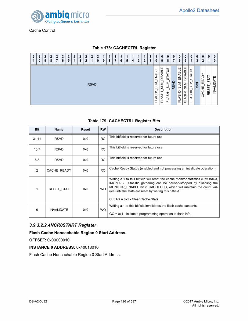
Apollo2 Datasheet
Cache Control
3.9.3.2.2.4NCR0START Register
Flash Cache Noncachable Region 0 Start Address.
OFFSET: 0x00000010
INSTANCE 0 ADDRESS: 0x40018010
Flash Cache Noncachable Region 0 Start Address.
Table 178: CACHECTRL Register
31
30
29
28
27
26
25
24
23
22
21
20
19
18
17
16
15
14
13
12
11
10
09
08
07
06
05
04
03
02
01
00
RSVD
FLA
SH
1_S
LM_E
NA
BLE
FLA
SH
1_S
LM_
DIS
AB
LE
FLA
SH
1_S
LM_S
TAT
US
RS
VD
FLA
SH
0_S
LM_E
NA
BLE
FLA
SH
0_S
LM_
DIS
AB
LE
FLA
SH
0_S
LM_S
TAT
US
RS
VD
CA
CH
E_
RE
AD
Y
RE
SE
T_S
TAT
INV
ALI
DA
TE
Table 179: CACHECTRL Register Bits
Bit Name Reset RW Description
31:11 RSVD 0x0 ROThis bitfield is reserved for future use.
10:7 RSVD 0x0 ROThis bitfield is reserved for future use.
6:3 RSVD 0x0 ROThis bitfield is reserved for future use.
2 CACHE_READY 0x0 ROCache Ready Status (enabled and not processing an invalidate operation)
1 RESET_STAT 0x0 WO
Writing a 1 to this bitfield will reset the cache monitor statistics (DMON0-3,IMON0-3). Statistic gathering can be paused/stopped by disabling theMONITOR_ENABLE bit in CACHECFG, which will maintain the count val-ues until the stats are reset by writing this bitfield.
CLEAR = 0x1 - Clear Cache Stats
0 INVALIDATE 0x0 WOWriting a 1 to this bitfield invalidates the flash cache contents.
GO = 0x1 - Initiate a programming operation to flash info.
DS-A2-0p92 Page 126 of 537 2017 Ambiq Micro, Inc.All rights reserved.

Apollo2 Datasheet
3.9.3.2.2.5NCR0END Register
Flash Cache Noncachable Region 0 End
OFFSET: 0x00000014
INSTANCE 0 ADDRESS: 0x40018014
Flash Cache Noncachable Region 0 End
Table 180: NCR0START Register
31
30
29
28
27
26
25
24
23
22
21
20
19
18
17
16
15
14
13
12
11
10
09
08
07
06
05
04
03
02
01
00
RSVD ADDR RSVD
Table 181: NCR0START Register Bits
Bit Name Reset RW Description
31:20 RSVD 0x0 ROThis bitfield is reserved for future use.
19:4 ADDR 0x0 RW
Start address for non-cacheable region 0. The physical address of the startof this region should be programmed to this register and must be aligned toa 16-byte boundary (thus the lower 4 address bits are unused).
3:0 RSVD 0x0 ROThis bitfield is reserved for future use.
Table 182: NCR0END Register
31
30
29
28
27
26
25
24
23
22
21
20
19
18
17
16
15
14
13
12
11
10
09
08
07
06
05
04
03
02
01
00
RSVD ADDR RSVD
Table 183: NCR0END Register Bits
Bit Name Reset RW Description
31:20 RSVD 0x0 ROThis bitfield is reserved for future use.
19:4 ADDR 0x0 RW
End address for non-cacheable region 0. The physical address of the endof this region should be programmed to this register and must be aligned toa 16-byte boundary (thus the lower 4 address bits are unused).
3:0 RSVD 0x0 ROThis bitfield is reserved for future use.
DS-A2-0p92 Page 127 of 537 2017 Ambiq Micro, Inc.All rights reserved.
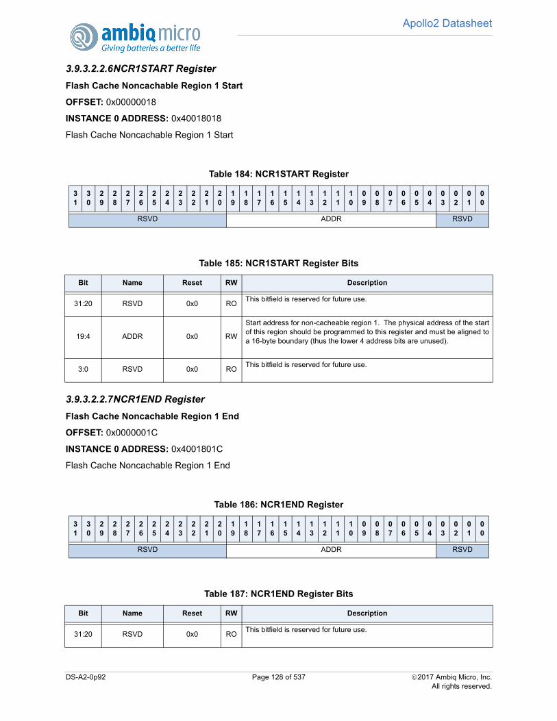
Apollo2 Datasheet
3.9.3.2.2.6NCR1START Register
Flash Cache Noncachable Region 1 Start
OFFSET: 0x00000018
INSTANCE 0 ADDRESS: 0x40018018
Flash Cache Noncachable Region 1 Start
3.9.3.2.2.7NCR1END Register
Flash Cache Noncachable Region 1 End
OFFSET: 0x0000001C
INSTANCE 0 ADDRESS: 0x4001801C
Flash Cache Noncachable Region 1 End
Table 184: NCR1START Register
31
30
29
28
27
26
25
24
23
22
21
20
19
18
17
16
15
14
13
12
11
10
09
08
07
06
05
04
03
02
01
00
RSVD ADDR RSVD
Table 185: NCR1START Register Bits
Bit Name Reset RW Description
31:20 RSVD 0x0 ROThis bitfield is reserved for future use.
19:4 ADDR 0x0 RW
Start address for non-cacheable region 1. The physical address of the startof this region should be programmed to this register and must be aligned toa 16-byte boundary (thus the lower 4 address bits are unused).
3:0 RSVD 0x0 ROThis bitfield is reserved for future use.
Table 186: NCR1END Register
31
30
29
28
27
26
25
24
23
22
21
20
19
18
17
16
15
14
13
12
11
10
09
08
07
06
05
04
03
02
01
00
RSVD ADDR RSVD
Table 187: NCR1END Register Bits
Bit Name Reset RW Description
31:20 RSVD 0x0 ROThis bitfield is reserved for future use.
DS-A2-0p92 Page 128 of 537 2017 Ambiq Micro, Inc.All rights reserved.
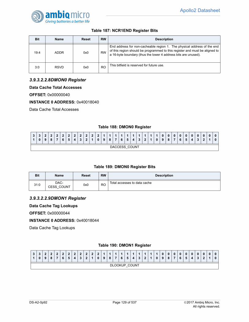
Apollo2 Datasheet
3.9.3.2.2.8DMON0 Register
Data Cache Total Accesses
OFFSET: 0x00000040
INSTANCE 0 ADDRESS: 0x40018040
Data Cache Total Accesses
3.9.3.2.2.9DMON1 Register
Data Cache Tag Lookups
OFFSET: 0x00000044
INSTANCE 0 ADDRESS: 0x40018044
Data Cache Tag Lookups
19:4 ADDR 0x0 RW
End address for non-cacheable region 1. The physical address of the endof this region should be programmed to this register and must be aligned toa 16-byte boundary (thus the lower 4 address bits are unused).
3:0 RSVD 0x0 ROThis bitfield is reserved for future use.
Table 188: DMON0 Register
31
30
29
28
27
26
25
24
23
22
21
20
19
18
17
16
15
14
13
12
11
10
09
08
07
06
05
04
03
02
01
00
DACCESS_COUNT
Table 189: DMON0 Register Bits
Bit Name Reset RW Description
31:0DAC-
CESS_COUNT0x0 RO
Total accesses to data cache
Table 190: DMON1 Register
31
30
29
28
27
26
25
24
23
22
21
20
19
18
17
16
15
14
13
12
11
10
09
08
07
06
05
04
03
02
01
00
DLOOKUP_COUNT
Table 187: NCR1END Register Bits
Bit Name Reset RW Description
DS-A2-0p92 Page 129 of 537 2017 Ambiq Micro, Inc.All rights reserved.
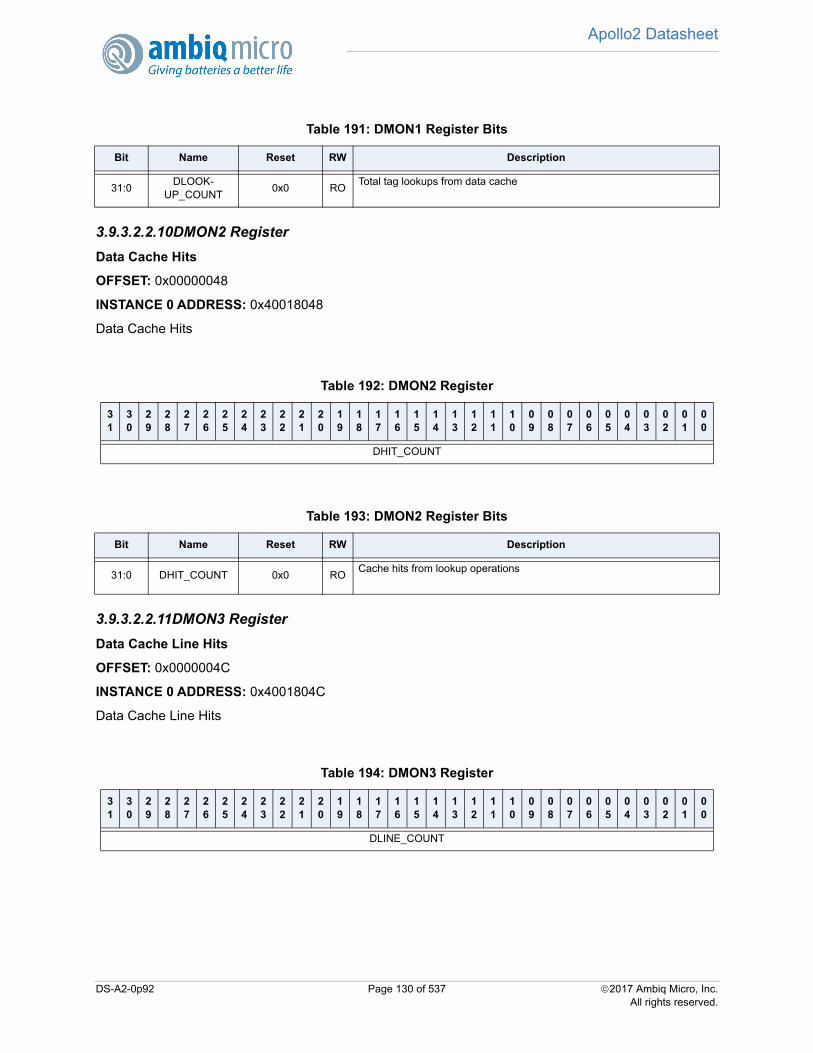
Apollo2 Datasheet
3.9.3.2.2.10DMON2 Register
Data Cache Hits
OFFSET: 0x00000048
INSTANCE 0 ADDRESS: 0x40018048
Data Cache Hits
3.9.3.2.2.11DMON3 Register
Data Cache Line Hits
OFFSET: 0x0000004C
INSTANCE 0 ADDRESS: 0x4001804C
Data Cache Line Hits
Table 191: DMON1 Register Bits
Bit Name Reset RW Description
31:0DLOOK-
UP_COUNT0x0 RO
Total tag lookups from data cache
Table 192: DMON2 Register
31
30
29
28
27
26
25
24
23
22
21
20
19
18
17
16
15
14
13
12
11
10
09
08
07
06
05
04
03
02
01
00
DHIT_COUNT
Table 193: DMON2 Register Bits
Bit Name Reset RW Description
31:0 DHIT_COUNT 0x0 ROCache hits from lookup operations
Table 194: DMON3 Register
31
30
29
28
27
26
25
24
23
22
21
20
19
18
17
16
15
14
13
12
11
10
09
08
07
06
05
04
03
02
01
00
DLINE_COUNT
DS-A2-0p92 Page 130 of 537 2017 Ambiq Micro, Inc.All rights reserved.
Apollo2 Datasheet
3.9.3.2.2.12IMON0 Register
Instruction Cache Total Accesses
OFFSET: 0x00000050
INSTANCE 0 ADDRESS: 0x40018050
Instruction Cache Total Accesses
3.9.3.2.2.13IMON1 Register
Instruction Cache Tag Lookups
OFFSET: 0x00000054
INSTANCE 0 ADDRESS: 0x40018054
Instruction Cache Tag Lookups
Table 195: DMON3 Register Bits
Bit Name Reset RW Description
31:0 DLINE_COUNT 0x0 ROCache hits from line cache
Table 196: IMON0 Register
31
30
29
28
27
26
25
24
23
22
21
20
19
18
17
16
15
14
13
12
11
10
09
08
07
06
05
04
03
02
01
00
IACCESS_COUNT
Table 197: IMON0 Register Bits
Bit Name Reset RW Description
31:0IAC-
CESS_COUNT0x0 RO
Total accesses to Instruction cache
Table 198: IMON1 Register
31
30
29
28
27
26
25
24
23
22
21
20
19
18
17
16
15
14
13
12
11
10
09
08
07
06
05
04
03
02
01
00
ILOOKUP_COUNT
DS-A2-0p92 Page 131 of 537 2017 Ambiq Micro, Inc.All rights reserved.
Apollo2 Datasheet
3.9.3.2.2.14IMON2 Register
Instruction Cache Hits
OFFSET: 0x00000058
INSTANCE 0 ADDRESS: 0x40018058
Instruction Cache Hits
3.9.3.2.2.15IMON3 Register
Instruction Cache Line Hits
OFFSET: 0x0000005C
INSTANCE 0 ADDRESS: 0x4001805C
Instruction Cache Line Hits
Table 199: IMON1 Register Bits
Bit Name Reset RW Description
31:0ILOOK-
UP_COUNT0x0 RO
Total tag lookups from Instruction cache
Table 200: IMON2 Register
31
30
29
28
27
26
25
24
23
22
21
20
19
18
17
16
15
14
13
12
11
10
09
08
07
06
05
04
03
02
01
00
IHIT_COUNT
Table 201: IMON2 Register Bits
Bit Name Reset RW Description
31:0 IHIT_COUNT 0x0 ROCache hits from lookup operations
Table 202: IMON3 Register
31
30
29
28
27
26
25
24
23
22
21
20
19
18
17
16
15
14
13
12
11
10
09
08
07
06
05
04
03
02
01
00
ILINE_COUNT
DS-A2-0p92 Page 132 of 537 2017 Ambiq Micro, Inc.All rights reserved.

Apollo2 Datasheet
3.9.3.3 Flash Memory Controller
Figure 7. Block diagram for the Flash Memory Controller
3.9.3.3.1 Functional Overview
During normal MCU code execution, the Flash Memory Controller translates requests from the CPU core(via the Flash cache) to the Flash Memory instance for instruction and data fetches. The Controller isdesigned to return data to the cache in single wait-state and can operate up to the maximum operatingfrequency of half the CPU core.
The Controller facilitates flash erase and programming operations through the control registers. Whenerase or programming operations are active, data cannot be fetched from the Flash memory. This will benaturely handled by the cache controller fill logic to stall until the program operation is complete and theFlash device is available. With the cache enabled, this collision should happen very infrequently.
Another function of the Controller is to capture the configuration values which are distributed to the variouson-chip peripherals of the MCU at chip power-up. These are read from the Information Space of the Flash
Table 203: IMON3 Register Bits
Bit Name Reset RW Description
31:0 ILINE_COUNT 0x0 ROCache hits from line cache
AHB Slave(Info Space)
APB Slave(Control Regs)
APB Slave(Config Regs)
ConfigRegisters
ControlRegisters
Timing Control
FlashInstance
Copy Engine
RequestTranslator
RequestTranslator
AHB Slave(DCode)
RequestTranslator
AHB Slave(ICode)
RequestTranslator
DS-A2-0p92 Page 133 of 537 2017 Ambiq Micro, Inc.All rights reserved.
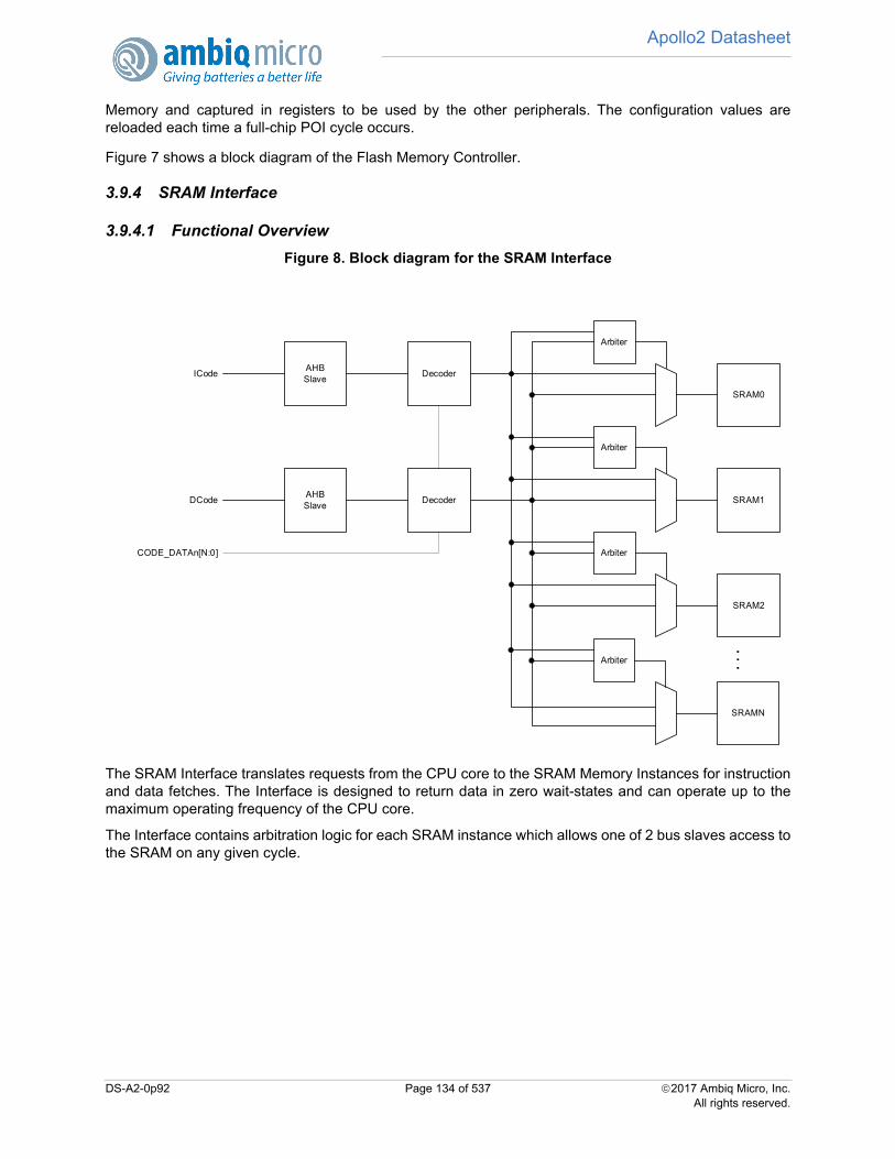
Apollo2 Datasheet
Memory and captured in registers to be used by the other peripherals. The configuration values arereloaded each time a full-chip POI cycle occurs.
Figure 7 shows a block diagram of the Flash Memory Controller.
3.9.4 SRAM Interface
3.9.4.1 Functional Overview
Figure 8. Block diagram for the SRAM Interface
The SRAM Interface translates requests from the CPU core to the SRAM Memory Instances for instructionand data fetches. The Interface is designed to return data in zero wait-states and can operate up to themaximum operating frequency of the CPU core.
The Interface contains arbitration logic for each SRAM instance which allows one of 2 bus slaves access tothe SRAM on any given cycle.
AHB Slave
Decoder
Arbiter
SRAM0
Arbiter
SRAM1
Arbiter
SRAM2
Arbiter
SRAMN
ICode
AHB Slave
DecoderDCode
CODE_DATAn[N:0]
. . .
DS-A2-0p92 Page 134 of 537 2017 Ambiq Micro, Inc.All rights reserved.

Apollo2 Datasheet
DS-A2-0p92 Page 135 of 537 2017 Ambiq Micro, Inc.All rights reserved.
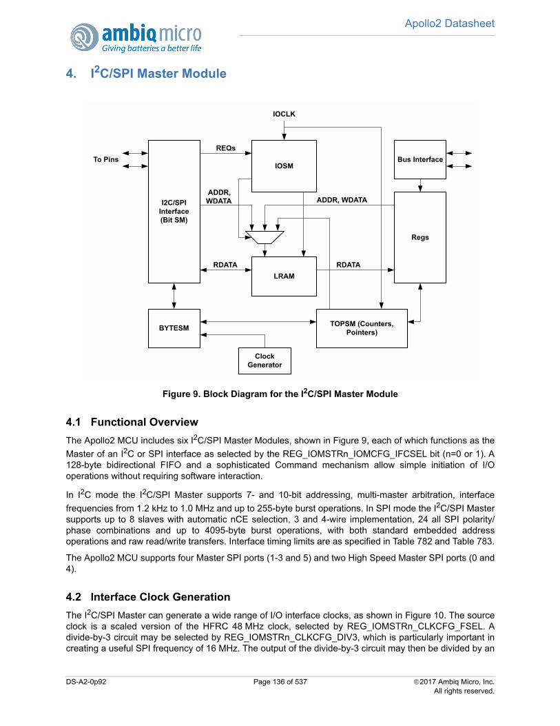
Apollo2 Datasheet
4. I2C/SPI Master Module
Figure 9. Block Diagram for the I2C/SPI Master Module
4.1 Functional Overview
The Apollo2 MCU includes six I2C/SPI Master Modules, shown in Figure 9, each of which functions as the
Master of an I2C or SPI interface as selected by the REG_IOMSTRn_IOMCFG_IFCSEL bit (n=0 or 1). A128-byte bidirectional FIFO and a sophisticated Command mechanism allow simple initiation of I/Ooperations without requiring software interaction.
In I2C mode the I2C/SPI Master supports 7- and 10-bit addressing, multi-master arbitration, interface
frequencies from 1.2 kHz to 1.0 MHz and up to 255-byte burst operations. In SPI mode the I2C/SPI Mastersupports up to 8 slaves with automatic nCE selection, 3 and 4-wire implementation, 24 all SPI polarity/phase combinations and up to 4095-byte burst operations, with both standard embedded addressoperations and raw read/write transfers. Interface timing limits are as specified in Table 782 and Table 783.
The Apollo2 MCU supports four Master SPI ports (1-3 and 5) and two High Speed Master SPI ports (0 and4).
4.2 Interface Clock Generation
The I2C/SPI Master can generate a wide range of I/O interface clocks, as shown in Figure 10. The sourceclock is a scaled version of the HFRC 48 MHz clock, selected by REG_IOMSTRn_CLKCFG_FSEL. Adivide-by-3 circuit may be selected by REG_IOMSTRn_CLKCFG_DIV3, which is particularly important increating a useful SPI frequency of 16 MHz. The output of the divide-by-3 circuit may then be divided by an
I2C/SPI Interface(Bit SM)
To PinsIOSM
LRAM
Bus InterfaceREQs
Ints
TOPSM (Counters, Pointers)
ADDR, WDATA
RDATA
ADDR, WDATA
RDATA
BYTESM
IOCLK
Clock Generator
Regs
DS-A2-0p92 Page 136 of 537 2017 Ambiq Micro, Inc.All rights reserved.
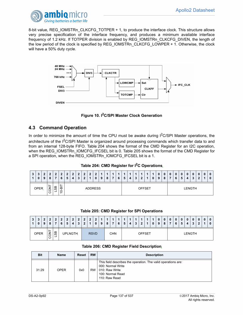
Apollo2 Datasheet
8-bit value, REG_IOMSTRn_CLKCFG_TOTPER + 1, to produce the interface clock. This structure allowsvery precise specification of the interface frequency, and produces a minimum available interfacefrequency of 1.2 kHz. If TOTPER division is enabled by REG_IOMSTRn_CLKCFG_DIVEN, the length ofthe low period of the clock is specified by REG_IOMSTRn_CLKCFG_LOWPER + 1. Otherwise, the clockwill have a 50% duty cycle.
Figure 10. I2C/SPI Master Clock Generation
4.3 Command Operation
In order to minimize the amount of time the CPU must be awake during I2C/SPI Master operations, the
architecture of the I2C/SPI Master is organized around processing commands which transfer data to andfrom an internal 128-byte FIFO. Table 204 shows the format of the CMD Register for an I2C operation,when the REG_IOMSTRn_IOMCFG_IFCSEL bit is 0. Table 205 shows the format of the CMD Register fora SPI operation, when the REG_IOMSTRn_IOMCFG_IFCSEL bit is a 1.
Table 204: CMD Register for I2C Operations
31
30
29
28
27
26
25
24
23
22
21
20
19
18
17
16
15
14
13
12
11
10
09
08
07
06
05
04
03
02
01
00
OPER
CO
NT
LSB
10-B
IT
ADDRESS OFFSET LENGTH
Table 205: CMD Register for SPI Operations
31
30
29
28
27
26
25
24
23
22
21
20
19
18
17
16
15
14
13
12
11
10
09
08
07
06
05
04
03
02
01
00
OPER
CO
NT
LSB UPLNGTH RSVD CHN OFFSET LENGTH
Table 206: CMD Register Field Description
Bit Name Reset RW Description
31:29 OPER 0x0 RW
This field describes the operation. The valid operations are:000: Normal Write010: Raw Write100: Normal Read110: Raw Read
24 MHz
768 kHz
... CLKCTR
LOWCMP
TOTCMP
CLKFF
Set
Clr
IFC_CLKFSEL
DIV3
DIV3
DIVEN
48 MHz
DS-A2-0p92 Page 137 of 537 2017 Ambiq Micro, Inc.All rights reserved.

Apollo2 Datasheet
For writes to the interface, software writes data to the FIFO (REG_IOMSTRn_FIFO_FIFO) and then sendsa single command to the REG_IOMSTRn_CMD Register. Unless the LENGTH field of the CMD is zero, atleast one word (4 bytes) of data must be written into the FIFO prior to writing the CMD Register or an ICMD
interrupt will be generated and the operation will be terminated.The Command includes either the I2Cslave address or the SPI channel select, the desired address offset and the length of the transfer. At that
point the I2C/SPI Master executes the entire transfer, so the CPU can go to sleep. If more than 128 bytesare to be transferred, the Master will generate a THR interrupt when the FIFOSIZ value,REG_IOMSTRn_FIFOPTR_FIFOSIZ, drops below the write threshold
REG_IOMSTRn_FIFOTHR_FIFOWTHR so the CPU can wake up and refill the FIFO. The I2C/SPI Masterwill generate the CMDCMP interrupt when the command is complete. In each case, the total number ofbytes transferred in each operation is specified in the LENGTH field of the CMD Register. If softwareexecutes a write to the FIFO when it is full (FIFOSIZ is greater than 124) the FOVFL interrupt will begenerated and the transfer will be terminated.
For reads, the CMD Register is first written with the command and the CPU can go to sleep. The Masterinitiates the read and transfers read data to the FIFO. If the FIFOSZ value exceeds the read thresholdREG_IOMSTRn_FIFOTHR_FIFORTHR, a THR interrupt is generated so the CPU can wake up and emptythe FIFO. A CMDCMP interrupt is also generated when the Command completes. If software executes aread from the FIFO when it has less than a word of data the FUNDFL interrupt will be generated and thetransfer will be terminated. FUNDFL will not be generated if the read transfer has already completed, sothat software can read the last FIFO word even if it is incomplete.
If the FIFO empties on a write or fills on a read, the I2C/SPI Master will simply pause the interface clockuntil the CPU has read or written a byte from the FIFO. This avoids the requirement that the thresholds be
28 CONT 0x0 RW If set to 1, the operation will be continued (see Section 4.5.12 and 4.6.8)
27 LSB 0x0 RWIf set to 0, data bytes are transferred most significant bit first. If set to 1, data bytes are transferred least significant bit first.
2610-BIT
(I2C ONLY)0x0 RW
If set to 1, 10-bit I2C addressing is used.
If set to 0, 7-bit I2C addressing is used.
25:16ADDRESS
(I2C ONLY)0x0 RW Address of the slave device on the I2C bus. If 7-bit addressing is specified, only
the lower 7 bits of this fields are used.
26:23UPLNGTH(SPI ONLY)
0x0 RWThis field contains the upper four bits of the 12-bit length field, allowing transfersup to 4095 bytes in SPI mode.
22:19RSVD
(SPI ONLY)0x0 RW RESERVED
18:16CHN
(SPI ONLY)0x0 RW
This field selects which of the eight nCE outputs will be asserted for this trans-
fer. This allows Apollo2 MCU to interface to up to eight separate SPI devices bysimply using different CHN values.
15:8 OFFSET 0x0 RW
In I2C mode, this field specifies the data transferred in the OFFSET byte forNormal Read and Write transfers.In SPI mode, this field specifies the first byte written in Normal Read and Writetransfers.
Raw transfers in either I2C or SPI mode do not use the OFFSET field.
7:0 LENGTH 0x0 RW
This field defines the length of the transfer in bytes. For Normal Read and Writeoperations, the LENGTH field may be set to 0, so that only the OFFSET byte iswritten and no other data is transferred. In SPI mode, the UPLNGTH field con-tains the upper 4 bits of the LENGTH so that up to 4095 bytes may be trans-ferred in a single operation.
Table 206: CMD Register Field Description
Bit Name Reset RW Description
DS-A2-0p92 Page 138 of 537 2017 Ambiq Micro, Inc.All rights reserved.
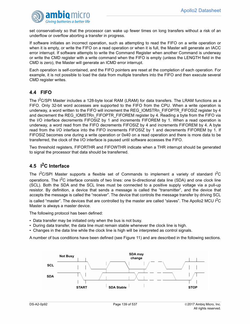
Apollo2 Datasheet
set conservatively so that the processor can wake up fewer times on long transfers without a risk of anunderflow or overflow aborting a transfer in progress.
If software initiates an incorrect operation, such as attempting to read the FIFO on a write operation orwhen it is empty, or write the FIFO on a read operation or when it is full, the Master will generate an IACCerror interrupt. If software attempts to write the Command Register when another Command is underwayor write the CMD register with a write command when the FIFO is empty (unless the LENGTH field in theCMD is zero), the Master will generate an ICMD error interrupt.
Each operation is self-contained, and the FIFO pointers are reset at the completion of each operation. Forexample, it is not possible to load the data from multiple transfers into the FIFO and then execute severalCMD register writes.
4.4 FIFO
The I2C/SPI Master includes a 128-byte local RAM (LRAM) for data transfers. The LRAM functions as aFIFO. Only 32-bit word accesses are supported to the FIFO from the CPU. When a write operation isunderway, a word written to the FIFO will increment the REG_IOMSTRn_FIFOPTR_FIFOSIZ register by 4and decrement the REG_IOMSTRn_FIFOPTR_FIFOREM register by 4. Reading a byte from the FIFO viathe I/O interface decrements FIFOSIZ by 1 and increments FIFOREM by 1. When a read operation isunderway, a word read from the FIFO decrements FIFOSIZ by 4 and increments FIFOREM by 4. A byteread from the I/O interface into the FIFO increments FIFOSIZ by 1 and decrements FIFOREM by 1. IfFIFOSIZ becomes one during a write operation or 0x40 on a read operation and there is more data to betransferred, the clock of the I/O interface is paused until software accesses the FIFO.
Two threshold registers, FIFORTHR and FIFOWTHR indicate when a THR interrupt should be generatedto signal the processor that data should be transferred.
4.5 I2C Interface
The I2C/SPI Master supports a flexible set of Commands to implement a variety of standard I2C
operations. The I2C interface consists of two lines: one bi-directional data line (SDA) and one clock line(SCL). Both the SDA and the SCL lines must be connected to a positive supply voltage via a pull-upresistor. By definition, a device that sends a message is called the “transmitter”, and the device thataccepts the message is called the “receiver”. The device that controls the message transfer by driving SCL
is called “master”. The devices that are controlled by the master are called “slaves”. The Apollo2 MCU I2CMaster is always a master device.
The following protocol has been defined:
Data transfer may be initiated only when the bus is not busy. During data transfer, the data line must remain stable whenever the clock line is high. Changes in the data line while the clock line is high will be interpreted as control signals.
A number of bus conditions have been defined (see Figure 11) and are described in the following sections.
SDA
SCL
START SDA Stable
SDA may change
STOP
Not Busy
DS-A2-0p92 Page 139 of 537 2017 Ambiq Micro, Inc.All rights reserved.
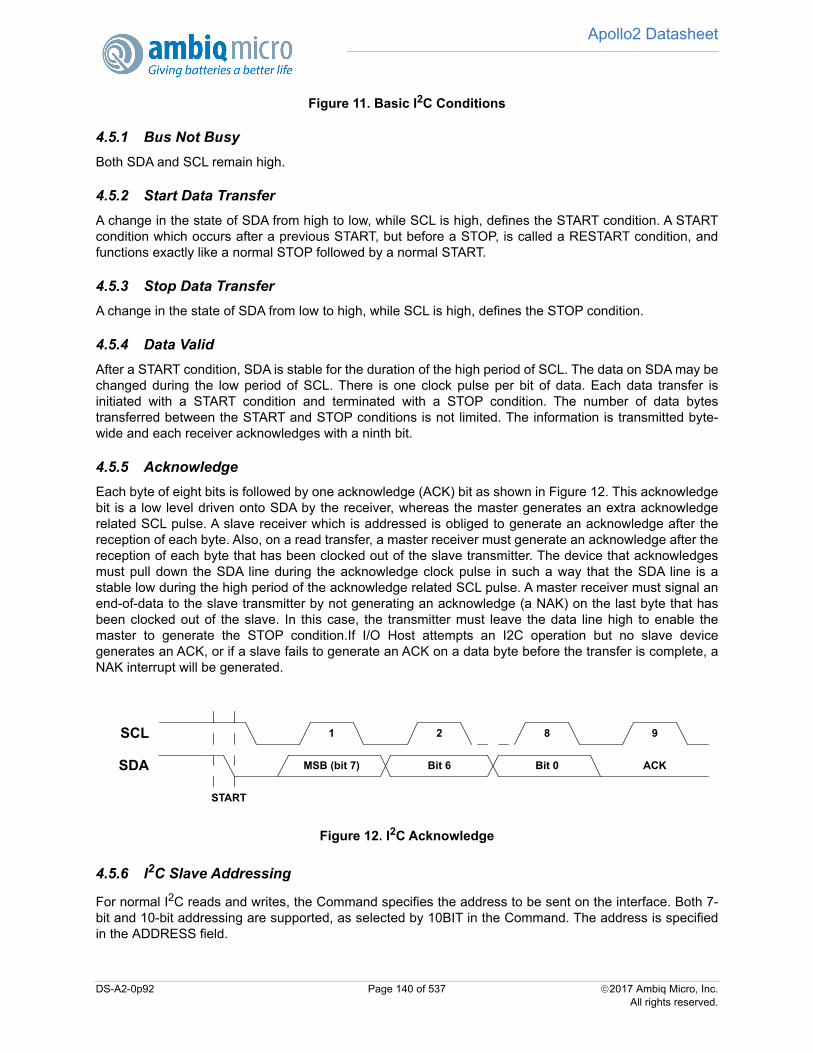
Apollo2 Datasheet
Figure 11. Basic I2C Conditions
4.5.1 Bus Not Busy
Both SDA and SCL remain high.
4.5.2 Start Data Transfer
A change in the state of SDA from high to low, while SCL is high, defines the START condition. A STARTcondition which occurs after a previous START, but before a STOP, is called a RESTART condition, andfunctions exactly like a normal STOP followed by a normal START.
4.5.3 Stop Data Transfer
A change in the state of SDA from low to high, while SCL is high, defines the STOP condition.
4.5.4 Data Valid
After a START condition, SDA is stable for the duration of the high period of SCL. The data on SDA may bechanged during the low period of SCL. There is one clock pulse per bit of data. Each data transfer isinitiated with a START condition and terminated with a STOP condition. The number of data bytestransferred between the START and STOP conditions is not limited. The information is transmitted byte-wide and each receiver acknowledges with a ninth bit.
4.5.5 Acknowledge
Each byte of eight bits is followed by one acknowledge (ACK) bit as shown in Figure 12. This acknowledgebit is a low level driven onto SDA by the receiver, whereas the master generates an extra acknowledgerelated SCL pulse. A slave receiver which is addressed is obliged to generate an acknowledge after thereception of each byte. Also, on a read transfer, a master receiver must generate an acknowledge after thereception of each byte that has been clocked out of the slave transmitter. The device that acknowledgesmust pull down the SDA line during the acknowledge clock pulse in such a way that the SDA line is astable low during the high period of the acknowledge related SCL pulse. A master receiver must signal anend-of-data to the slave transmitter by not generating an acknowledge (a NAK) on the last byte that hasbeen clocked out of the slave. In this case, the transmitter must leave the data line high to enable themaster to generate the STOP condition.If I/O Host attempts an I2C operation but no slave devicegenerates an ACK, or if a slave fails to generate an ACK on a data byte before the transfer is complete, aNAK interrupt will be generated.
Figure 12. I2C Acknowledge
4.5.6 I2C Slave Addressing
For normal I2C reads and writes, the Command specifies the address to be sent on the interface. Both 7-bit and 10-bit addressing are supported, as selected by 10BIT in the Command. The address is specifiedin the ADDRESS field.
SDA
SCL
START
MSB (bit 7) Bit 6 Bit 0 ACK
1 2 8 9
DS-A2-0p92 Page 140 of 537 2017 Ambiq Micro, Inc.All rights reserved.
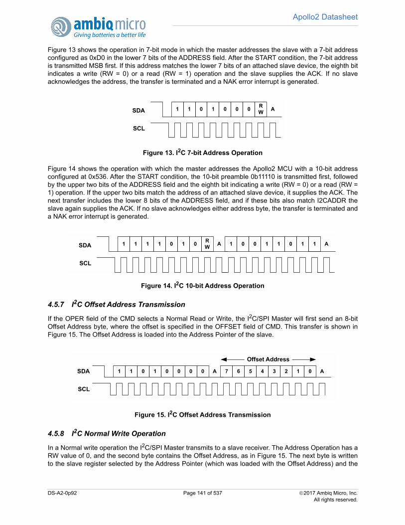
Apollo2 Datasheet
Figure 13 shows the operation in 7-bit mode in which the master addresses the slave with a 7-bit addressconfigured as 0xD0 in the lower 7 bits of the ADDRESS field. After the START condition, the 7-bit addressis transmitted MSB first. If this address matches the lower 7 bits of an attached slave device, the eighth bitindicates a write (RW = 0) or a read (RW = 1) operation and the slave supplies the ACK. If no slaveacknowledges the address, the transfer is terminated and a NAK error interrupt is generated.
Figure 13. I2C 7-bit Address Operation
Figure 14 shows the operation with which the master addresses the Apollo2 MCU with a 10-bit addressconfigured at 0x536. After the START condition, the 10-bit preamble 0b11110 is transmitted first, followedby the upper two bits of the ADDRESS field and the eighth bit indicating a write (RW = 0) or a read (RW =1) operation. If the upper two bits match the address of an attached slave device, it supplies the ACK. Thenext transfer includes the lower 8 bits of the ADDRESS field, and if these bits also match I2CADDR theslave again supplies the ACK. If no slave acknowledges either address byte, the transfer is terminated anda NAK error interrupt is generated.
Figure 14. I2C 10-bit Address Operation
4.5.7 I2C Offset Address Transmission
If the OPER field of the CMD selects a Normal Read or Write, the I2C/SPI Master will first send an 8-bitOffset Address byte, where the offset is specified in the OFFSET field of CMD. This transfer is shown inFigure 15. The Offset Address is loaded into the Address Pointer of the slave.
Figure 15. I2C Offset Address Transmission
4.5.8 I2C Normal Write Operation
In a Normal write operation the I2C/SPI Master transmits to a slave receiver. The Address Operation has aRW value of 0, and the second byte contains the Offset Address, as in Figure 15. The next byte is writtento the slave register selected by the Address Pointer (which was loaded with the Offset Address) and the
A1 1 0 1 0 0 0SDA
SCL
RW
A1 1 1 1 0 1 0SDA
SCL
RW A1 0 0 1 1 0 1 1
A1 1 0SDA
SCL
0 A7 6 1 0
Offset Address
0 1 0 0 5 4 3 2
DS-A2-0p92 Page 141 of 537 2017 Ambiq Micro, Inc.All rights reserved.
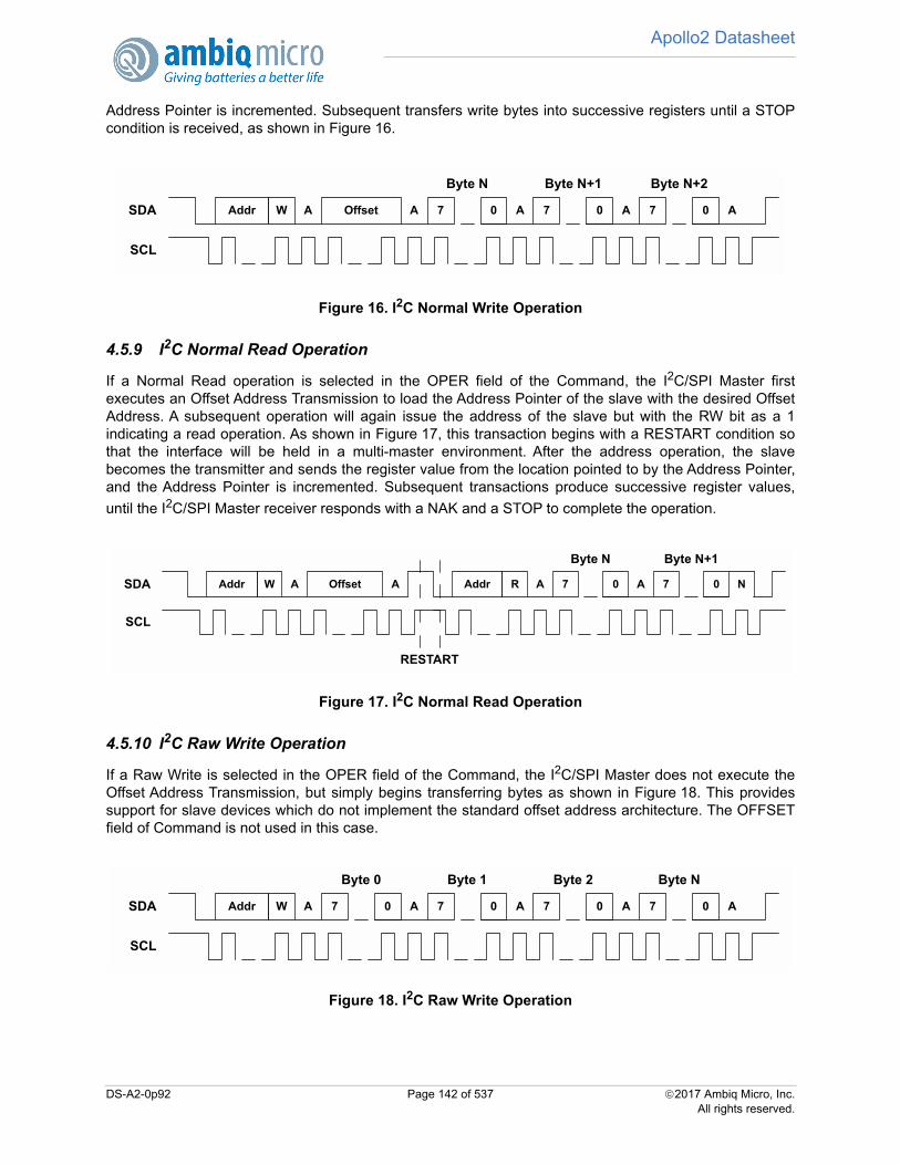
Apollo2 Datasheet
Address Pointer is incremented. Subsequent transfers write bytes into successive registers until a STOPcondition is received, as shown in Figure 16.
Figure 16. I2C Normal Write Operation
4.5.9 I2C Normal Read Operation
If a Normal Read operation is selected in the OPER field of the Command, the I2C/SPI Master firstexecutes an Offset Address Transmission to load the Address Pointer of the slave with the desired OffsetAddress. A subsequent operation will again issue the address of the slave but with the RW bit as a 1indicating a read operation. As shown in Figure 17, this transaction begins with a RESTART condition sothat the interface will be held in a multi-master environment. After the address operation, the slavebecomes the transmitter and sends the register value from the location pointed to by the Address Pointer,and the Address Pointer is incremented. Subsequent transactions produce successive register values,
until the I2C/SPI Master receiver responds with a NAK and a STOP to complete the operation.
Figure 17. I2C Normal Read Operation
4.5.10 I2C Raw Write Operation
If a Raw Write is selected in the OPER field of the Command, the I2C/SPI Master does not execute theOffset Address Transmission, but simply begins transferring bytes as shown in Figure 18. This providessupport for slave devices which do not implement the standard offset address architecture. The OFFSETfield of Command is not used in this case.
Figure 18. I2C Raw Write Operation
Addr OffsetSDA
SCL
7 0
Byte N
AW A A 7 0
Byte N+1
A 7 0
Byte N+2
A
SDA
SCL
7 0
Byte N
A A 7 0
Byte N+1
NAddr AR
RESTART
Addr OffsetAW
AddrSDA
SCL
7 0
Byte 1
AW A 7 0
Byte 2
A 7 0
Byte N
A7 0
Byte 0
A
DS-A2-0p92 Page 142 of 537 2017 Ambiq Micro, Inc.All rights reserved.
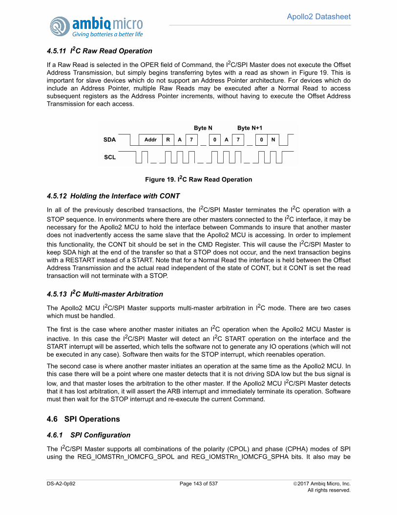
Apollo2 Datasheet
4.5.11 I2C Raw Read Operation
If a Raw Read is selected in the OPER field of Command, the I2C/SPI Master does not execute the OffsetAddress Transmission, but simply begins transferring bytes with a read as shown in Figure 19. This isimportant for slave devices which do not support an Address Pointer architecture. For devices which doinclude an Address Pointer, multiple Raw Reads may be executed after a Normal Read to accesssubsequent registers as the Address Pointer increments, without having to execute the Offset AddressTransmission for each access.
Figure 19. I2C Raw Read Operation
4.5.12 Holding the Interface with CONT
In all of the previously described transactions, the I2C/SPI Master terminates the I2C operation with a
STOP sequence. In environments where there are other masters connected to the I2C interface, it may benecessary for the Apollo2 MCU to hold the interface between Commands to insure that another masterdoes not inadvertently access the same slave that the Apollo2 MCU is accessing. In order to implement
this functionality, the CONT bit should be set in the CMD Register. This will cause the I2C/SPI Master tokeep SDA high at the end of the transfer so that a STOP does not occur, and the next transaction beginswith a RESTART instead of a START. Note that for a Normal Read the interface is held between the OffsetAddress Transmission and the actual read independent of the state of CONT, but it CONT is set the readtransaction will not terminate with a STOP.
4.5.13 I2C Multi-master Arbitration
The Apollo2 MCU I2C/SPI Master supports multi-master arbitration in I2C mode. There are two caseswhich must be handled.
The first is the case where another master initiates an I2C operation when the Apollo2 MCU Master is
inactive. In this case the I2C/SPI Master will detect an I2C START operation on the interface and theSTART interrupt will be asserted, which tells the software not to generate any IO operations (which will notbe executed in any case). Software then waits for the STOP interrupt, which reenables operation.
The second case is where another master initiates an operation at the same time as the Apollo2 MCU. Inthis case there will be a point where one master detects that it is not driving SDA low but the bus signal is
low, and that master loses the arbitration to the other master. If the Apollo2 MCU I2C/SPI Master detectsthat it has lost arbitration, it will assert the ARB interrupt and immediately terminate its operation. Softwaremust then wait for the STOP interrupt and re-execute the current Command.
4.6 SPI Operations
4.6.1 SPI Configuration
The I2C/SPI Master supports all combinations of the polarity (CPOL) and phase (CPHA) modes of SPIusing the REG_IOMSTRn_IOMCFG_SPOL and REG_IOMSTRn_IOMCFG_SPHA bits. It also may be
SDA
SCL
7 0
Byte N
A 7 0
Byte N+1
NAddr AR
DS-A2-0p92 Page 143 of 537 2017 Ambiq Micro, Inc.All rights reserved.
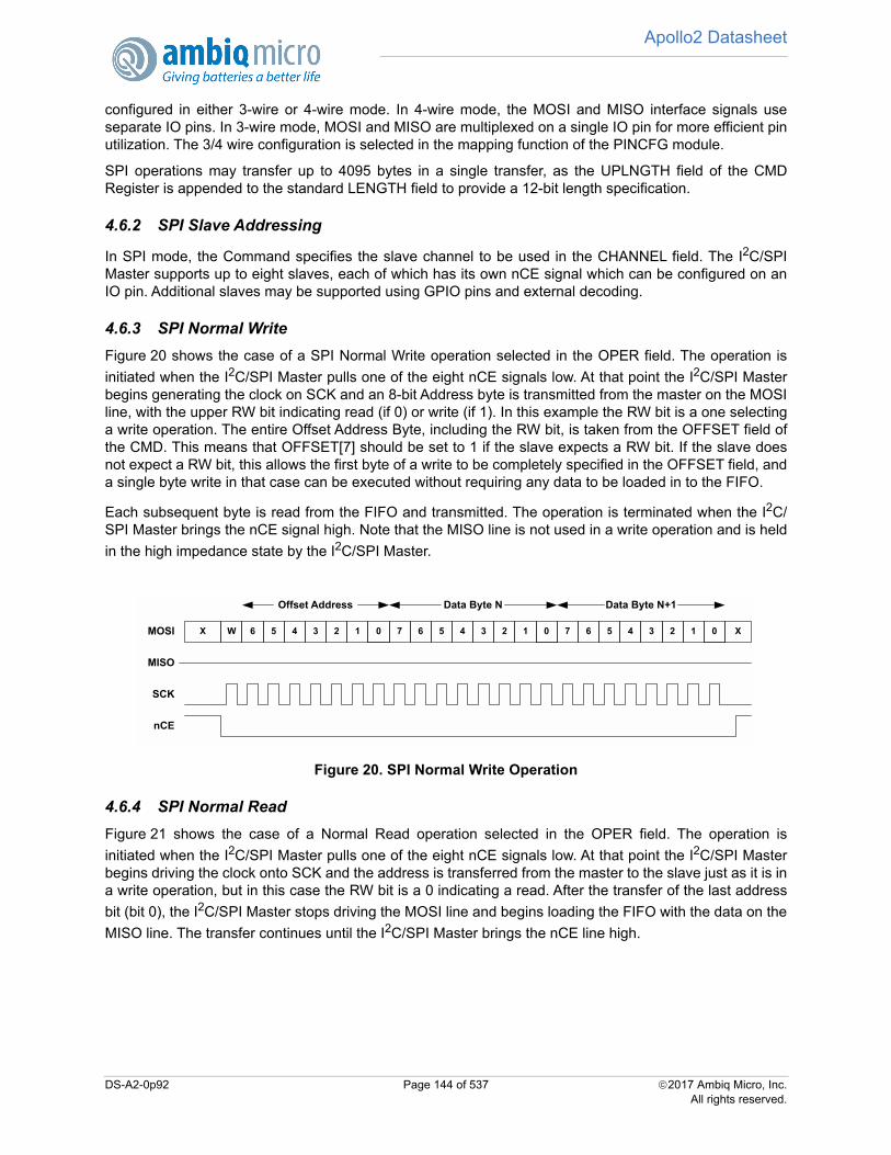
Apollo2 Datasheet
configured in either 3-wire or 4-wire mode. In 4-wire mode, the MOSI and MISO interface signals useseparate IO pins. In 3-wire mode, MOSI and MISO are multiplexed on a single IO pin for more efficient pinutilization. The 3/4 wire configuration is selected in the mapping function of the PINCFG module.
SPI operations may transfer up to 4095 bytes in a single transfer, as the UPLNGTH field of the CMDRegister is appended to the standard LENGTH field to provide a 12-bit length specification.
4.6.2 SPI Slave Addressing
In SPI mode, the Command specifies the slave channel to be used in the CHANNEL field. The I2C/SPIMaster supports up to eight slaves, each of which has its own nCE signal which can be configured on anIO pin. Additional slaves may be supported using GPIO pins and external decoding.
4.6.3 SPI Normal Write
Figure 20 shows the case of a SPI Normal Write operation selected in the OPER field. The operation is
initiated when the I2C/SPI Master pulls one of the eight nCE signals low. At that point the I2C/SPI Masterbegins generating the clock on SCK and an 8-bit Address byte is transmitted from the master on the MOSIline, with the upper RW bit indicating read (if 0) or write (if 1). In this example the RW bit is a one selectinga write operation. The entire Offset Address Byte, including the RW bit, is taken from the OFFSET field ofthe CMD. This means that OFFSET[7] should be set to 1 if the slave expects a RW bit. If the slave doesnot expect a RW bit, this allows the first byte of a write to be completely specified in the OFFSET field, anda single byte write in that case can be executed without requiring any data to be loaded in to the FIFO.
Each subsequent byte is read from the FIFO and transmitted. The operation is terminated when the I2C/SPI Master brings the nCE signal high. Note that the MISO line is not used in a write operation and is held
in the high impedance state by the I2C/SPI Master.
Figure 20. SPI Normal Write Operation
4.6.4 SPI Normal Read
Figure 21 shows the case of a Normal Read operation selected in the OPER field. The operation is
initiated when the I2C/SPI Master pulls one of the eight nCE signals low. At that point the I2C/SPI Masterbegins driving the clock onto SCK and the address is transferred from the master to the slave just as it is ina write operation, but in this case the RW bit is a 0 indicating a read. After the transfer of the last address
bit (bit 0), the I2C/SPI Master stops driving the MOSI line and begins loading the FIFO with the data on the
MISO line. The transfer continues until the I2C/SPI Master brings the nCE line high.
W 6 1MOSI
SCK
0 7 6 1 0
Offset Address
nCE
X
Data Byte N
7 6 1 0
Data Byte N+1
X
MISO
5 4 3 2 5 4 3 2 5 4 3 2
DS-A2-0p92 Page 144 of 537 2017 Ambiq Micro, Inc.All rights reserved.

Apollo2 Datasheet
Figure 21. SPI Normal Read Operation
As with a Normal Write, the Offset Address byte including the RW bit is taken from the OFFSET field ofCMD. If the slave expects an RW bit, OFFSET[7] must be set to 1. This allows reads from devices whichhave different formats for the address byte.
4.6.5 SPI Raw Write
If a Raw Write is selected in the OPER field, the operation is similar to a Normal Write but the OffsetAddress byte is not sent and all data comes directly from the FIFO as shown in Figure 22. The OFFSETfield is not used in this case.
Figure 22. SPI Raw Write Operation
4.6.6 SPI Raw Read
If a Raw Read is selected in the OPER field, the operation is simply the data transfer portion of a NormalRead. All data goes directly to the FIFO as shown in Figure 23. The OFFSET field is not used in this case.
Figure 23. SPI Raw Read Operation
R 6 1MOSI
SCK
0
Offset Address
nCE
X
Data Byte N Data Byte N+1
7 6 1 0 7 6 1 0MISO
X5 4 3 2
5 4 3 2 5 4 3 2
7 6 1MOSI
SCK
0 7 6 1 0
nCE
X 7 6 1 0
Data Byte N+2
X
MISO
5 4 3 2 5 4 3 2 5 4 3 2
Data Byte N+1Data Byte N
MOSI
SCK
nCE
Data Byte N+2
7 6 1 0 7 6 1 0MISO 5 4 3 2 5 4 3 2
Data Byte N+1
7 6 1 05 4 3 2
Data Byte N
DS-A2-0p92 Page 145 of 537 2017 Ambiq Micro, Inc.All rights reserved.

Apollo2 Datasheet
4.6.7 SPI 3-wire Mode
In 3-wire mode, the MOSI and MISO lines are shared on a single pin. As described in the previoussections, the MISO and MOSI lines are not driven at the same time, so 3-wire mode is equivalent to simplytying them together external to the Apollo2 MCU. 3-wire mode is configured by selecting the MxWIR3alternative (x = 0 to 5 selecting the I2C/SPI Master) in the GPIO Pad Multiplexor rather than the MxMOSIand MxMISO alternatives. Detailed configuration information is supplied in the GPIO and PadConfiguration Module chapter.
4.6.8 Complex SPI Operations
In some cases peripheral devices require more complex transaction sequences than those supported by asingle Command. In order to support these transactions, the CONT bit may be set in the Command. In thiscase, the nCE pin selected by the Channel will remain asserted low at the end of the transaction, so thatthe next SPI operation will be seen as part of the same transaction. For example, there are peripheraldevices which require both a Function and an Address Offset to be transmitted at the beginning of a read.Implementing this can be done in several ways. One example as shown in Figure 24 is:
1. Execute a Raw SPI write of length 2, with the data bytes being the Function and Offset. Set the CONT bit in this Command so nCE remains asserted low.
2. Execute a Raw SPI Read of the desired transfer length. The data will then be read into the FIFO. The CONT bit is not set in this Command.
Figure 24. SPI Combined Operation
4.6.9 SPI Polarity and Phase
The Apollo2 MCU supports all combinations of CPOL (clock polarity) and CPHA (data phase) in SPI mode,as defined by the SPOL and SPHA bits. Figure 25 shows how these two bits affect the interface signalbehavior.
7 6 1MOSI
SCK
0 7 6 1 0
Function
nCE
X
Offset Address
7 6 1 0
Read Data
X
MISO
5 4 3 2 5 4 3 2
5 4 3 2
Raw Write, 2 Bytes Raw Read, 1 Byte
DS-A2-0p92 Page 146 of 537 2017 Ambiq Micro, Inc.All rights reserved.
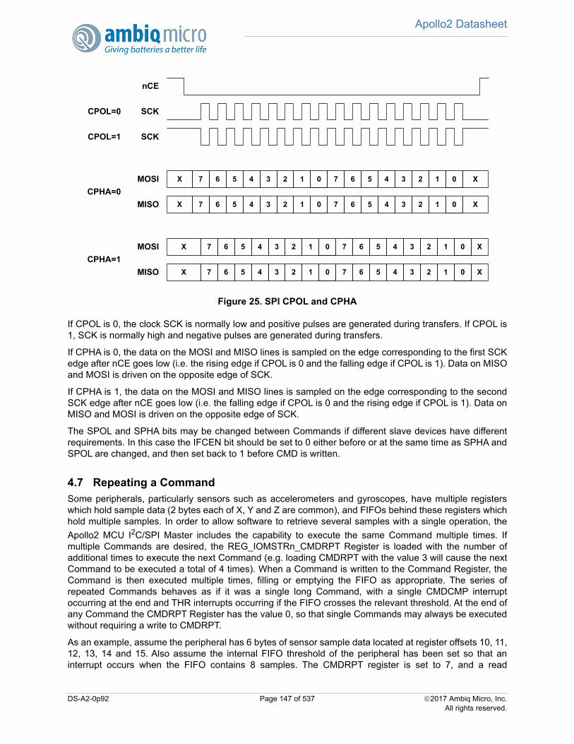
Apollo2 Datasheet
Figure 25. SPI CPOL and CPHA
If CPOL is 0, the clock SCK is normally low and positive pulses are generated during transfers. If CPOL is1, SCK is normally high and negative pulses are generated during transfers.
If CPHA is 0, the data on the MOSI and MISO lines is sampled on the edge corresponding to the first SCKedge after nCE goes low (i.e. the rising edge if CPOL is 0 and the falling edge if CPOL is 1). Data on MISOand MOSI is driven on the opposite edge of SCK.
If CPHA is 1, the data on the MOSI and MISO lines is sampled on the edge corresponding to the secondSCK edge after nCE goes low (i.e. the falling edge if CPOL is 0 and the rising edge if CPOL is 1). Data onMISO and MOSI is driven on the opposite edge of SCK.
The SPOL and SPHA bits may be changed between Commands if different slave devices have differentrequirements. In this case the IFCEN bit should be set to 0 either before or at the same time as SPHA andSPOL are changed, and then set back to 1 before CMD is written.
4.7 Repeating a CommandSome peripherals, particularly sensors such as accelerometers and gyroscopes, have multiple registerswhich hold sample data (2 bytes each of X, Y and Z are common), and FIFOs behind these registers whichhold multiple samples. In order to allow software to retrieve several samples with a single operation, the
Apollo2 MCU I2C/SPI Master includes the capability to execute the same Command multiple times. Ifmultiple Commands are desired, the REG_IOMSTRn_CMDRPT Register is loaded with the number ofadditional times to execute the next Command (e.g. loading CMDRPT with the value 3 will cause the nextCommand to be executed a total of 4 times). When a Command is written to the Command Register, theCommand is then executed multiple times, filling or emptying the FIFO as appropriate. The series ofrepeated Commands behaves as if it was a single long Command, with a single CMDCMP interruptoccurring at the end and THR interrupts occurring if the FIFO crosses the relevant threshold. At the end ofany Command the CMDRPT Register has the value 0, so that single Commands may always be executedwithout requiring a write to CMDRPT.
As an example, assume the peripheral has 6 bytes of sensor sample data located at register offsets 10, 11,12, 13, 14 and 15. Also assume the internal FIFO threshold of the peripheral has been set so that aninterrupt occurs when the FIFO contains 8 samples. The CMDRPT register is set to 7, and a read
CPOL=0
CPOL=1
7 6 1MOSI 0 7 6 1 0X 5 4 3 2 5 4 3 2
7 6 1MISO 0 7 6 1 0X 5 4 3 2 5 4 3 2
SCK
7 6 1MOSI 0 7 6 1 0X 5 4 3 2 5 4 3 2
7 6 1MISO 0 7 6 1 0X 5 4 3 2 5 4 3 2
CPHA=0
CPHA=1
X
X
X
X
SCK
nCE
DS-A2-0p92 Page 147 of 537 2017 Ambiq Micro, Inc.All rights reserved.

Apollo2 Datasheet
Command is executed with an offset of 10 and a length of 6. This Command will be executed 8 times, each
time bursting 6 bytes of data from registers 10-15 in the peripheral to the I2C/SPI Master FIFO. When
CMDCMP is received the FIFO in the I2C/SPI Master will contain 48 bytes of data. The bytes of data arepacked in the FIFO – there are no gaps between samples.
4.8 Bit Orientation
In both I2C and SPI modes, the I2C/SPI Master supports data transmission either LSB first or MSB first asconfigured by the LSB bit in the Command. If LSB is 0, data is transmitted and received MSB first. If LSB is1, data is transmitted and received LSB first.
4.9 Full Duplex OperationsSome SPI slaves operate in full duplex mode, where data is transferred on both the MISO and MOSI wires
at the same time. The I2C/SPI Master supports this type of operation when theREG_IOMSTRn_IOMCFG_FULLDUP bit is set.
When FULLDUP is set, the I2C/SPI Master splits the standard 128-byte transmit/receive FIFO into a 64-byte transmit FIFO and a 64-byte receive FIFO. A normal or raw write Command is executed, andproceeds just as a normal write transfer. FIFOREM will report the remaining FIFO area as the remainderfrom 64 bytes. Software must not attempt to load more than 64 bytes into the write FIFO or an IACC errorwill be generated. The primary difference from a normal write operation is that data received on the MISOline will be loaded into the read FIFO, with the bytes aligned to the corresponding byte in the write FIFO.Software may read the read FIFO at any time, and should use the FIFOSIZ and./or FIFOREM registers todetermine when data should be read. The FIFORTHR threshold value does not generate an interrupt.
If more than 64 bytes of data are written into the read FIFO without being read by software, the read FIFOwill simply wrap around and overwrite the earlier read data. This means that if a long full duplex operationonly returns data at the end, software does not need to continuously empty the read FIFO but can simplydrain the FIFO when the write operation is complete.
4.10 SPI Flow Control
The I2C/SPI Master supports flow control from the slave, which is controlled by several configuration bits.Either read or write (or both) flow control may be implemented. Read flow control is enabled by setting the
REG_IOMSTRn_IOMCFG_RDFC bit, in which case the I2C/SPI Master will check the state of the FlowControl IRQ pin, and if it is inactive the SPI clock will stop at the completion of the current byte transfer untilit becomes active. The Flow Control IRQ can be any of the 50 pins as selected by the
REG_GPIO_IOMnIRQ register corresponding to the particular I2C/SPI Master. The polarity of the activestate of the Flow Control IRQ is selected by the REG_IOMSTRn_IOMCFG_RDFCPOL
Write flow control is enabled by setting the REG_IOMSTRn_IOMCFG_WTFC bit, but in this case either theFlow Control IRQ or the state of the MISO line may be used for flow control, as selected by theREG_IOMSTRn_IOMCFG_WTFCIRQ bit. If IRQ is selected by setting a one, the clock control is identicalto that described for reads above and the IRQ polarity is set by the REG_IOMSTRn_IOMCFG_WTFCPOLbit. If MISO is selected by setting a zero in WTFCIRQ, the clock will be stopped if the MISO line is at theinactive polarity, which is set by the WTFCPOL bit.
Slave devices supporting flow control typically require specific states of the MOSI line prior to the start of atransfer. This state is controlled by the REG_IOMSTRn_IOMCFG_MOSIINV bit. If this bit is zero, MOSI willbe driven to a 1 at the start of a write transaction and to a 0 at the start of a read transaction – this is thenormal operation of devices with flow control support. If MOSIINV is set to one, these polarities will beinverted.
DS-A2-0p92 Page 148 of 537 2017 Ambiq Micro, Inc.All rights reserved.
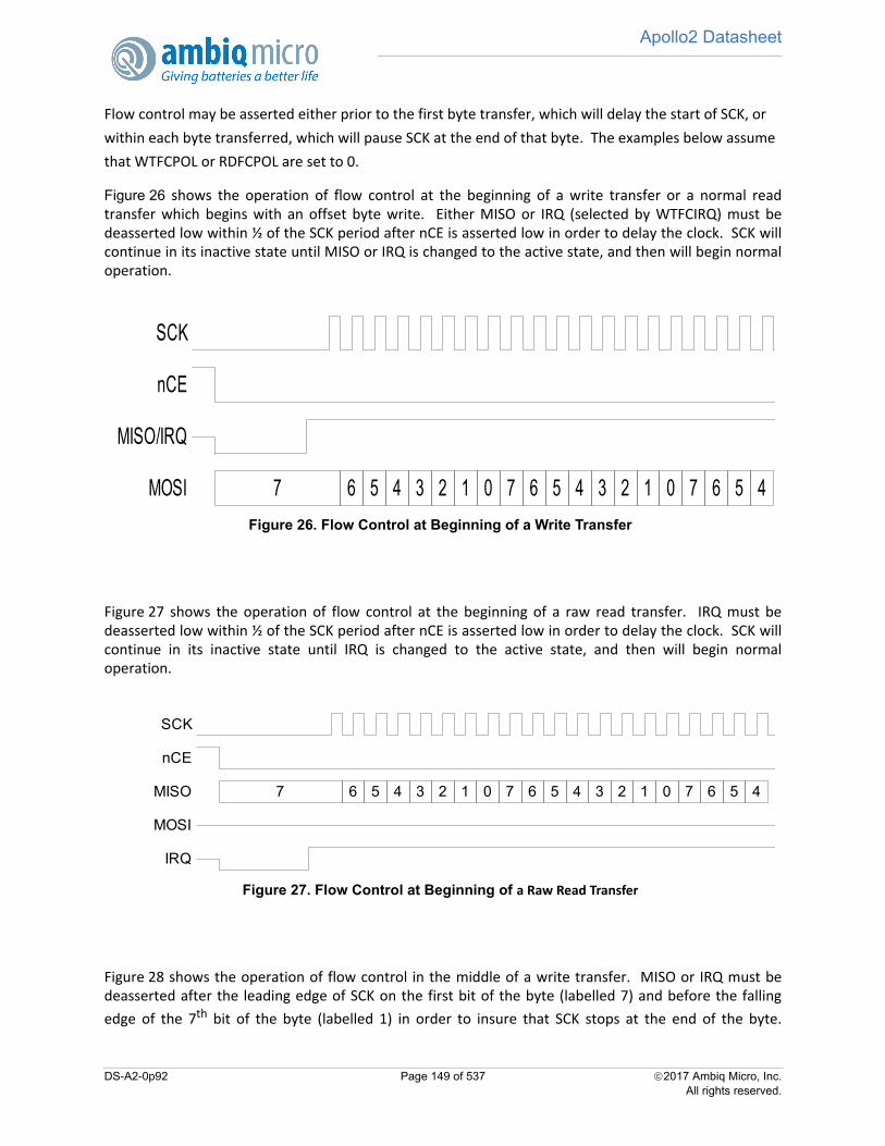
Apollo2 Datasheet
Flow control may be asserted either prior to the first byte transfer, which will delay the start of SCK, or
within each byte transferred, which will pause SCK at the end of that byte. The examples below assume
that WTFCPOL or RDFCPOL are set to 0.
Figure 26 shows the operation of flow control at the beginning of a write transfer or a normal readtransfer which begins with an offset byte write. Either MISO or IRQ (selected by WTFCIRQ) must bedeasserted low within ½ of the SCK period after nCE is asserted low in order to delay the clock. SCK willcontinue in its inactive state until MISO or IRQ is changed to the active state, and then will begin normaloperation.
Figure 27 shows the operation of flow control at the beginning of a raw read transfer. IRQ must bedeasserted low within ½ of the SCK period after nCE is asserted low in order to delay the clock. SCK willcontinue in its inactive state until IRQ is changed to the active state, and then will begin normaloperation.
Figure 28 shows the operation of flow control in the middle of a write transfer. MISO or IRQ must bedeasserted after the leading edge of SCK on the first bit of the byte (labelled 7) and before the falling
edge of the 7th bit of the byte (labelled 1) in order to insure that SCK stops at the end of the byte.
SCK
nCE
MISO/IRQ
MOSI 7 6 5 4 3 2 1 0 7 6 5 4 3 2 1 0 7 6 5 4
Figure 26. Flow Control at Beginning of a Write Transfer
Figure 27. Flow Control at Beginning of a Raw Read Transfer
SCK
nCE
MISO
MOSI
7 6 5 4 3 2 1 0 7 6 5 4 3 2 1 0 7 6 5 4
IRQ
DS-A2-0p92 Page 149 of 537 2017 Ambiq Micro, Inc.All rights reserved.
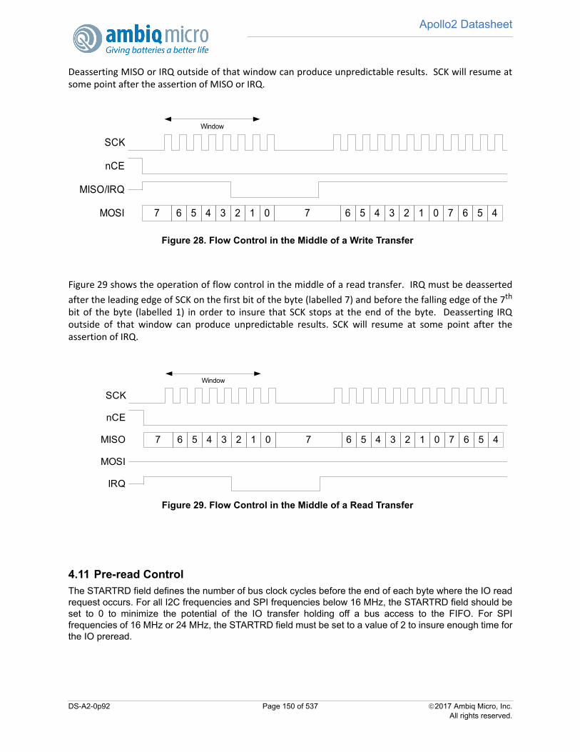
Apollo2 Datasheet
Deasserting MISO or IRQ outside of that window can produce unpredictable results. SCK will resume atsome point after the assertion of MISO or IRQ.
Figure 29 shows the operation of flow control in the middle of a read transfer. IRQ must be deasserted
after the leading edge of SCK on the first bit of the byte (labelled 7) and before the falling edge of the 7th
bit of the byte (labelled 1) in order to insure that SCK stops at the end of the byte. Deasserting IRQoutside of that window can produce unpredictable results. SCK will resume at some point after theassertion of IRQ.
4.11 Pre-read ControlThe STARTRD field defines the number of bus clock cycles before the end of each byte where the IO readrequest occurs. For all I2C frequencies and SPI frequencies below 16 MHz, the STARTRD field should beset to 0 to minimize the potential of the IO transfer holding off a bus access to the FIFO. For SPIfrequencies of 16 MHz or 24 MHz, the STARTRD field must be set to a value of 2 to insure enough time forthe IO preread.
Figure 28. Flow Control in the Middle of a Write Transfer
SCK
nCE
MOSI 7 6 5 4 3 2 1 0 7 6 5 4 3 2 1 0 7 6 5 4
MISO/IRQ
Window
Figure 29. Flow Control in the Middle of a Read Transfer
SCK
nCE
MOSI
7 6 5 4 3 2 1 0 7 6 5 4 3 2 1 0 7 6 5 4
IRQ
MISO
Window
DS-A2-0p92 Page 150 of 537 2017 Ambiq Micro, Inc.All rights reserved.
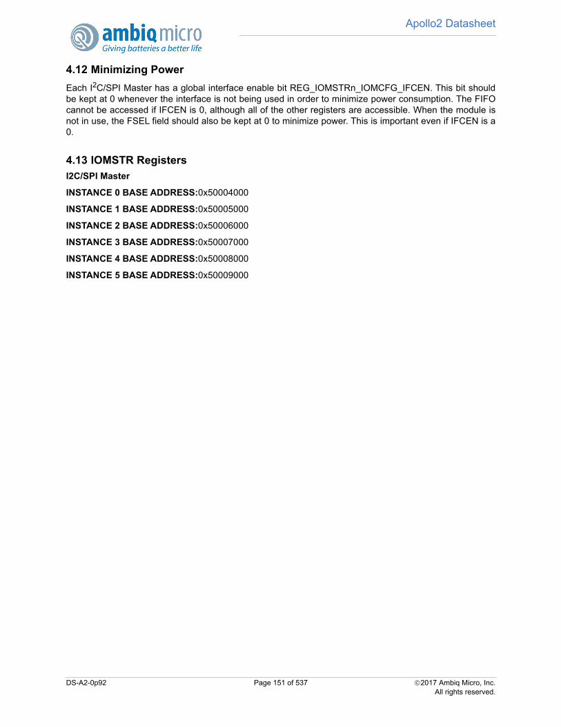
Apollo2 Datasheet
4.12 Minimizing Power
Each I2C/SPI Master has a global interface enable bit REG_IOMSTRn_IOMCFG_IFCEN. This bit shouldbe kept at 0 whenever the interface is not being used in order to minimize power consumption. The FIFOcannot be accessed if IFCEN is 0, although all of the other registers are accessible. When the module isnot in use, the FSEL field should also be kept at 0 to minimize power. This is important even if IFCEN is a0.
4.13 IOMSTR RegistersI2C/SPI Master
INSTANCE 0 BASE ADDRESS:0x50004000
INSTANCE 1 BASE ADDRESS:0x50005000
INSTANCE 2 BASE ADDRESS:0x50006000
INSTANCE 3 BASE ADDRESS:0x50007000
INSTANCE 4 BASE ADDRESS:0x50008000
INSTANCE 5 BASE ADDRESS:0x50009000
DS-A2-0p92 Page 151 of 537 2017 Ambiq Micro, Inc.All rights reserved.

Apollo2 Datasheet
4.13.1 Register Memory Map
Table 207: IOMSTR Register Map
Address(s) Register Name Description
0x500040000x500050000x500060000x500070000x500080000x50009000
FIFO FIFO Access Port
0x500041000x500051000x500061000x500071000x500081000x50009100
FIFOPTR Current FIFO Pointers
0x500041040x500051040x500061040x500071040x500081040x50009104
TLNGTH Transfer Length
0x500041080x500051080x500061080x500071080x500081080x50009108
FIFOTHR FIFO Threshold Configuration
0x5000410C0x5000510C0x5000610C0x5000710C0x5000810C0x5000910C
CLKCFG I/O Clock Configuration
0x500041100x500051100x500061100x500071100x500081100x50009110
CMD Command Register
0x500041140x500051140x500061140x500071140x500081140x50009114
CMDRPT Command Repeat Register
0x500041180x500051180x500061180x500071180x500081180x50009118
STATUS Status Register
DS-A2-0p92 Page 152 of 537 2017 Ambiq Micro, Inc.All rights reserved.
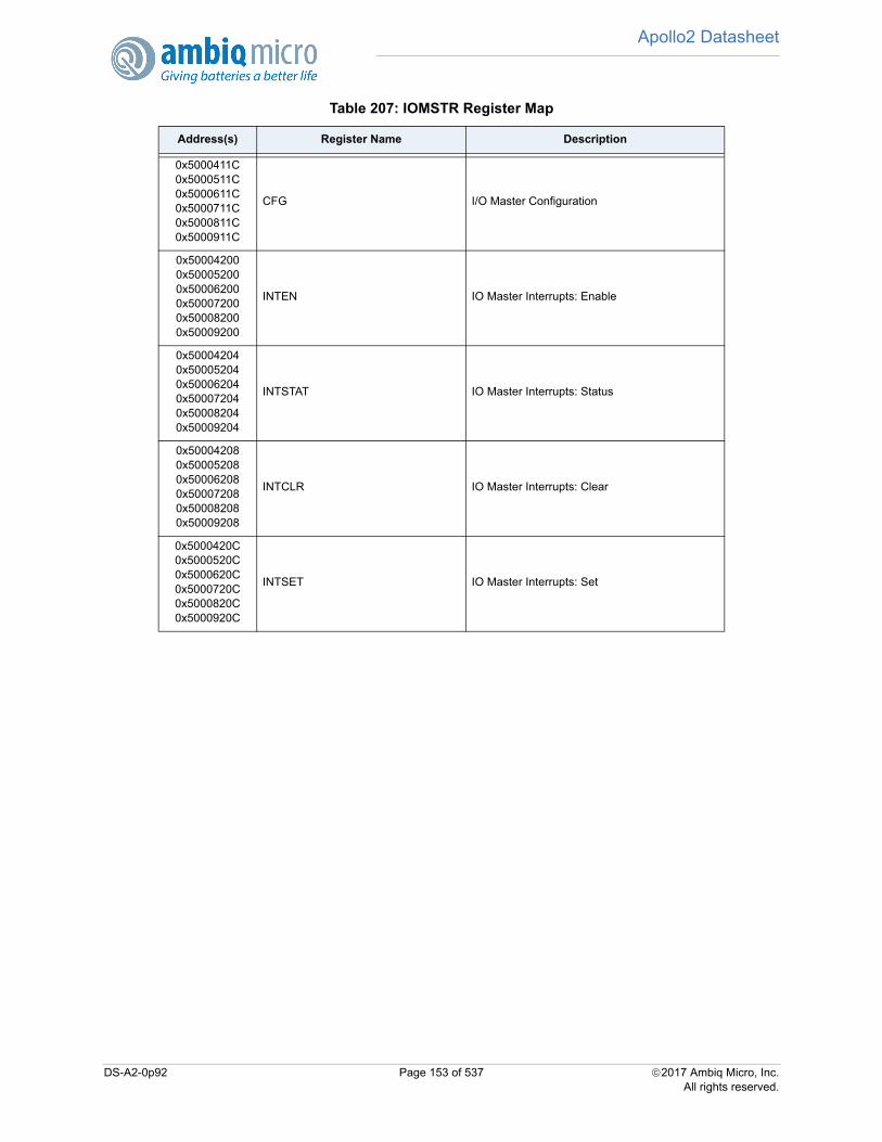
Apollo2 Datasheet
0x5000411C0x5000511C0x5000611C0x5000711C0x5000811C0x5000911C
CFG I/O Master Configuration
0x500042000x500052000x500062000x500072000x500082000x50009200
INTEN IO Master Interrupts: Enable
0x500042040x500052040x500062040x500072040x500082040x50009204
INTSTAT IO Master Interrupts: Status
0x500042080x500052080x500062080x500072080x500082080x50009208
INTCLR IO Master Interrupts: Clear
0x5000420C0x5000520C0x5000620C0x5000720C0x5000820C0x5000920C
INTSET IO Master Interrupts: Set
Table 207: IOMSTR Register Map
Address(s) Register Name Description
DS-A2-0p92 Page 153 of 537 2017 Ambiq Micro, Inc.All rights reserved.
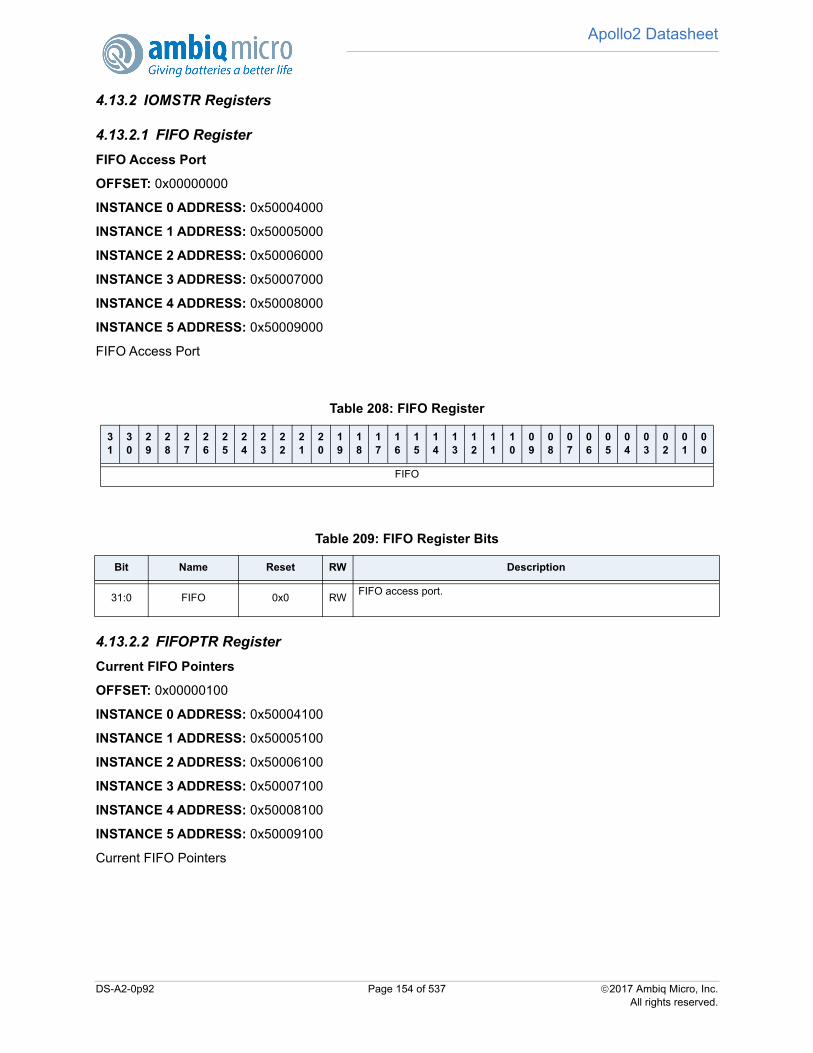
Apollo2 Datasheet
4.13.2 IOMSTR Registers
4.13.2.1 FIFO Register
FIFO Access Port
OFFSET: 0x00000000
INSTANCE 0 ADDRESS: 0x50004000
INSTANCE 1 ADDRESS: 0x50005000
INSTANCE 2 ADDRESS: 0x50006000
INSTANCE 3 ADDRESS: 0x50007000
INSTANCE 4 ADDRESS: 0x50008000
INSTANCE 5 ADDRESS: 0x50009000
FIFO Access Port
4.13.2.2 FIFOPTR Register
Current FIFO Pointers
OFFSET: 0x00000100
INSTANCE 0 ADDRESS: 0x50004100
INSTANCE 1 ADDRESS: 0x50005100
INSTANCE 2 ADDRESS: 0x50006100
INSTANCE 3 ADDRESS: 0x50007100
INSTANCE 4 ADDRESS: 0x50008100
INSTANCE 5 ADDRESS: 0x50009100
Current FIFO Pointers
Table 208: FIFO Register
31
30
29
28
27
26
25
24
23
22
21
20
19
18
17
16
15
14
13
12
11
10
09
08
07
06
05
04
03
02
01
00
FIFO
Table 209: FIFO Register Bits
Bit Name Reset RW Description
31:0 FIFO 0x0 RWFIFO access port.
DS-A2-0p92 Page 154 of 537 2017 Ambiq Micro, Inc.All rights reserved.
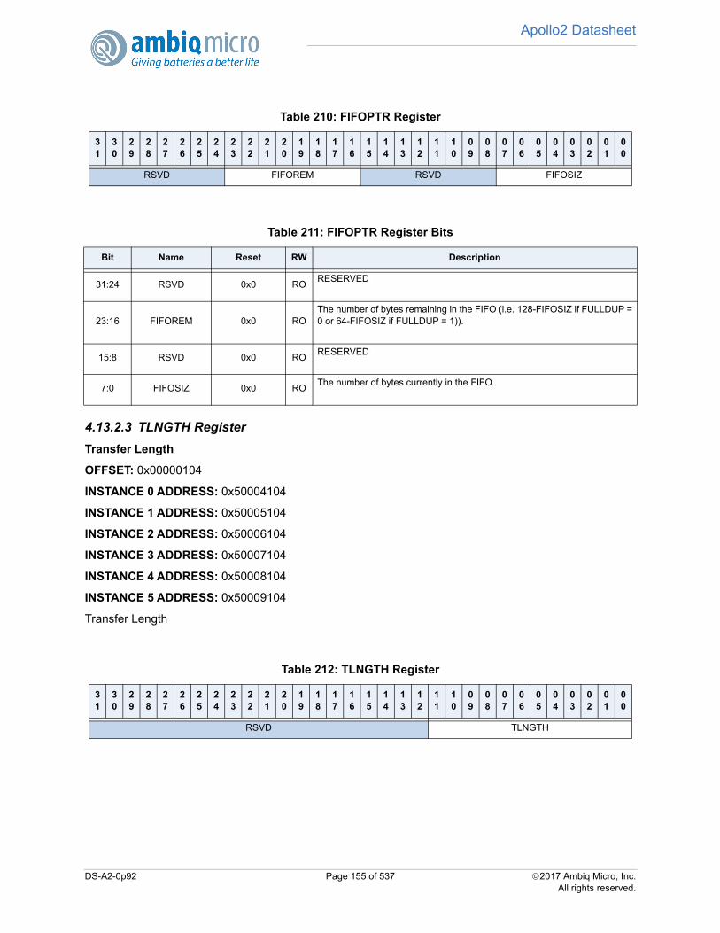
Apollo2 Datasheet
4.13.2.3 TLNGTH Register
Transfer Length
OFFSET: 0x00000104
INSTANCE 0 ADDRESS: 0x50004104
INSTANCE 1 ADDRESS: 0x50005104
INSTANCE 2 ADDRESS: 0x50006104
INSTANCE 3 ADDRESS: 0x50007104
INSTANCE 4 ADDRESS: 0x50008104
INSTANCE 5 ADDRESS: 0x50009104
Transfer Length
Table 210: FIFOPTR Register
31
30
29
28
27
26
25
24
23
22
21
20
19
18
17
16
15
14
13
12
11
10
09
08
07
06
05
04
03
02
01
00
RSVD FIFOREM RSVD FIFOSIZ
Table 211: FIFOPTR Register Bits
Bit Name Reset RW Description
31:24 RSVD 0x0 RORESERVED
23:16 FIFOREM 0x0 ROThe number of bytes remaining in the FIFO (i.e. 128-FIFOSIZ if FULLDUP =0 or 64-FIFOSIZ if FULLDUP = 1)).
15:8 RSVD 0x0 RORESERVED
7:0 FIFOSIZ 0x0 ROThe number of bytes currently in the FIFO.
Table 212: TLNGTH Register
31
30
29
28
27
26
25
24
23
22
21
20
19
18
17
16
15
14
13
12
11
10
09
08
07
06
05
04
03
02
01
00
RSVD TLNGTH
DS-A2-0p92 Page 155 of 537 2017 Ambiq Micro, Inc.All rights reserved.

Apollo2 Datasheet
4.13.2.4 FIFOTHR Register
FIFO Threshold Configuration
OFFSET: 0x00000108
INSTANCE 0 ADDRESS: 0x50004108
INSTANCE 1 ADDRESS: 0x50005108
INSTANCE 2 ADDRESS: 0x50006108
INSTANCE 3 ADDRESS: 0x50007108
INSTANCE 4 ADDRESS: 0x50008108
INSTANCE 5 ADDRESS: 0x50009108
FIFO Threshold Configuration
4.13.2.5 CLKCFG Register
I/O Clock Configuration
OFFSET: 0x0000010C
Table 213: TLNGTH Register Bits
Bit Name Reset RW Description
31:12 RSVD 0x0 RORESERVED
11:0 TLNGTH 0x0 RORemaining transfer length.
Table 214: FIFOTHR Register
31
30
29
28
27
26
25
24
23
22
21
20
19
18
17
16
15
14
13
12
11
10
09
08
07
06
05
04
03
02
01
00
RSVD FIFOWTHR
RS
VD
FIFORTHR
Table 215: FIFOTHR Register Bits
Bit Name Reset RW Description
31:15 RSVD 0x0 RORESERVED
14:8 FIFOWTHR 0x0 RWFIFO write threshold.
7 RSVD 0x0 RORESERVED
6:0 FIFORTHR 0x0 RWFIFO read threshold.
DS-A2-0p92 Page 156 of 537 2017 Ambiq Micro, Inc.All rights reserved.
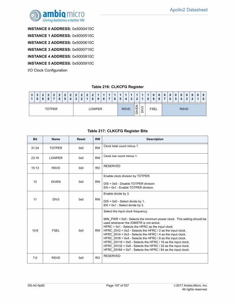
Apollo2 Datasheet
INSTANCE 0 ADDRESS: 0x5000410C
INSTANCE 1 ADDRESS: 0x5000510C
INSTANCE 2 ADDRESS: 0x5000610C
INSTANCE 3 ADDRESS: 0x5000710C
INSTANCE 4 ADDRESS: 0x5000810C
INSTANCE 5 ADDRESS: 0x5000910C
I/O Clock Configuration
Table 216: CLKCFG Register
31
30
29
28
27
26
25
24
23
22
21
20
19
18
17
16
15
14
13
12
11
10
09
08
07
06
05
04
03
02
01
00
TOTPER LOWPER RSVD
DIV
EN
DIV
3
FSEL RSVD
Table 217: CLKCFG Register Bits
Bit Name Reset RW Description
31:24 TOTPER 0x0 RWClock total count minus 1.
23:16 LOWPER 0x0 RWClock low count minus 1.
15:13 RSVD 0x0 RORESERVED
12 DIVEN 0x0 RW
Enable clock division by TOTPER.
DIS = 0x0 - Disable TOTPER division.EN = 0x1 - Enable TOTPER division.
11 DIV3 0x0 RW
Enable divide by 3.
DIS = 0x0 - Select divide by 1.EN = 0x1 - Select divide by 3.
10:8 FSEL 0x0 RW
Select the input clock frequency.
MIN_PWR = 0x0 - Selects the minimum power clock. This setting should beused whenever the IOMSTR is not active.HFRC = 0x1 - Selects the HFRC as the input clock.HFRC_DIV2 = 0x2 - Selects the HFRC / 2 as the input clock.HFRC_DIV4 = 0x3 - Selects the HFRC / 4 as the input clock.HFRC_DIV8 = 0x4 - Selects the HFRC / 8 as the input clock.HFRC_DIV16 = 0x5 - Selects the HFRC / 16 as the input clock.HFRC_DIV32 = 0x6 - Selects the HFRC / 32 as the input clock.HFRC_DIV64 = 0x7 - Selects the HFRC / 64 as the input clock.
7:0 RSVD 0x0 RORESERVED
DS-A2-0p92 Page 157 of 537 2017 Ambiq Micro, Inc.All rights reserved.

Apollo2 Datasheet
4.13.2.6 CMD Register
Command Register
OFFSET: 0x00000110
INSTANCE 0 ADDRESS: 0x50004110
INSTANCE 1 ADDRESS: 0x50005110
INSTANCE 2 ADDRESS: 0x50006110
INSTANCE 3 ADDRESS: 0x50007110
INSTANCE 4 ADDRESS: 0x50008110
INSTANCE 5 ADDRESS: 0x50009110
Command Register
4.13.2.7 CMDRPT Register
Command Repeat Register
OFFSET: 0x00000114
INSTANCE 0 ADDRESS: 0x50004114
INSTANCE 1 ADDRESS: 0x50005114
INSTANCE 2 ADDRESS: 0x50006114
INSTANCE 3 ADDRESS: 0x50007114
INSTANCE 4 ADDRESS: 0x50008114
INSTANCE 5 ADDRESS: 0x50009114
Command Repeat Register
Table 218: CMD Register
31
30
29
28
27
26
25
24
23
22
21
20
19
18
17
16
15
14
13
12
11
10
09
08
07
06
05
04
03
02
01
00
CMD
Table 219: CMD Register Bits
Bit Name Reset RW Description
31:0 CMD 0x0 RWThis register holds the I/O Command
DS-A2-0p92 Page 158 of 537 2017 Ambiq Micro, Inc.All rights reserved.
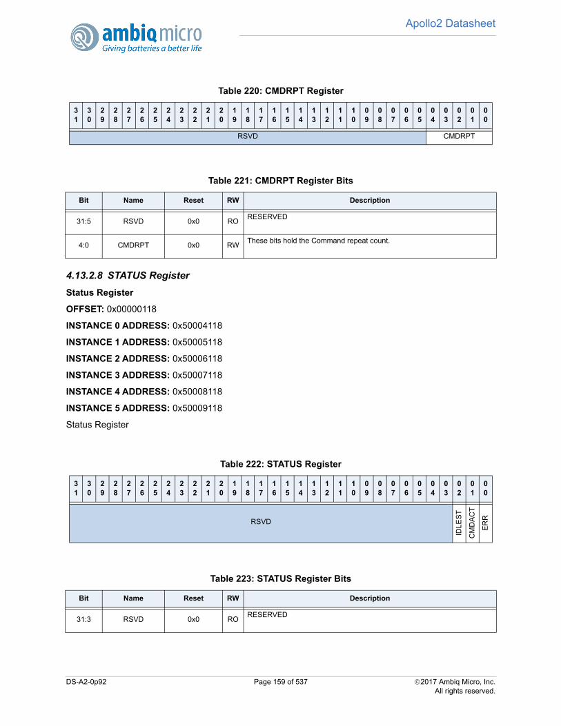
Apollo2 Datasheet
4.13.2.8 STATUS Register
Status Register
OFFSET: 0x00000118
INSTANCE 0 ADDRESS: 0x50004118
INSTANCE 1 ADDRESS: 0x50005118
INSTANCE 2 ADDRESS: 0x50006118
INSTANCE 3 ADDRESS: 0x50007118
INSTANCE 4 ADDRESS: 0x50008118
INSTANCE 5 ADDRESS: 0x50009118
Status Register
Table 220: CMDRPT Register
31
30
29
28
27
26
25
24
23
22
21
20
19
18
17
16
15
14
13
12
11
10
09
08
07
06
05
04
03
02
01
00
RSVD CMDRPT
Table 221: CMDRPT Register Bits
Bit Name Reset RW Description
31:5 RSVD 0x0 RORESERVED
4:0 CMDRPT 0x0 RWThese bits hold the Command repeat count.
Table 222: STATUS Register
31
30
29
28
27
26
25
24
23
22
21
20
19
18
17
16
15
14
13
12
11
10
09
08
07
06
05
04
03
02
01
00
RSVD
IDLE
ST
CM
DA
CT
ER
R
Table 223: STATUS Register Bits
Bit Name Reset RW Description
31:3 RSVD 0x0 RORESERVED
DS-A2-0p92 Page 159 of 537 2017 Ambiq Micro, Inc.All rights reserved.
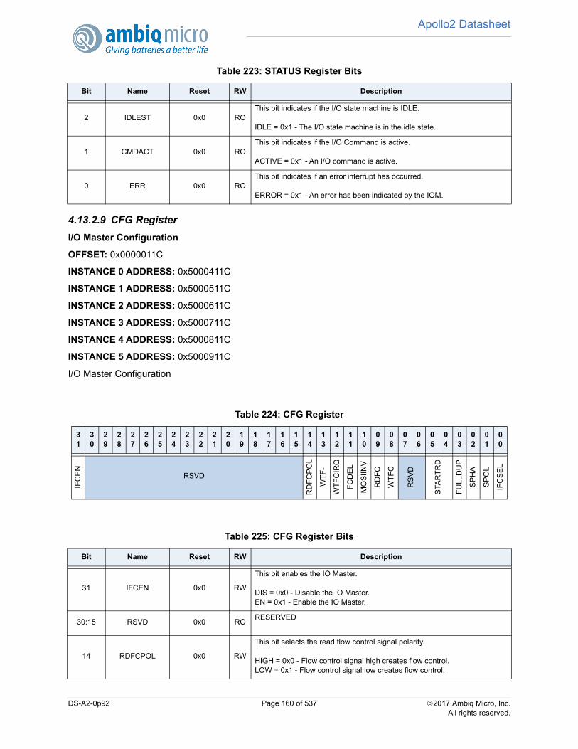
Apollo2 Datasheet
4.13.2.9 CFG Register
I/O Master Configuration
OFFSET: 0x0000011C
INSTANCE 0 ADDRESS: 0x5000411C
INSTANCE 1 ADDRESS: 0x5000511C
INSTANCE 2 ADDRESS: 0x5000611C
INSTANCE 3 ADDRESS: 0x5000711C
INSTANCE 4 ADDRESS: 0x5000811C
INSTANCE 5 ADDRESS: 0x5000911C
I/O Master Configuration
2 IDLEST 0x0 ROThis bit indicates if the I/O state machine is IDLE.
IDLE = 0x1 - The I/O state machine is in the idle state.
1 CMDACT 0x0 ROThis bit indicates if the I/O Command is active.
ACTIVE = 0x1 - An I/O command is active.
0 ERR 0x0 ROThis bit indicates if an error interrupt has occurred.
ERROR = 0x1 - An error has been indicated by the IOM.
Table 224: CFG Register
31
30
29
28
27
26
25
24
23
22
21
20
19
18
17
16
15
14
13
12
11
10
09
08
07
06
05
04
03
02
01
00
IFC
EN
RSVD
RD
FC
PO
L
WT
F-
WT
FC
IRQ
FC
DE
L
MO
SII
NV
RD
FC
WT
FC
RS
VD
STA
RT
RD
FU
LLD
UP
SP
HA
SP
OL
IFC
SE
L
Table 225: CFG Register Bits
Bit Name Reset RW Description
31 IFCEN 0x0 RW
This bit enables the IO Master.
DIS = 0x0 - Disable the IO Master.EN = 0x1 - Enable the IO Master.
30:15 RSVD 0x0 RORESERVED
14 RDFCPOL 0x0 RW
This bit selects the read flow control signal polarity.
HIGH = 0x0 - Flow control signal high creates flow control.LOW = 0x1 - Flow control signal low creates flow control.
Table 223: STATUS Register Bits
Bit Name Reset RW Description
DS-A2-0p92 Page 160 of 537 2017 Ambiq Micro, Inc.All rights reserved.
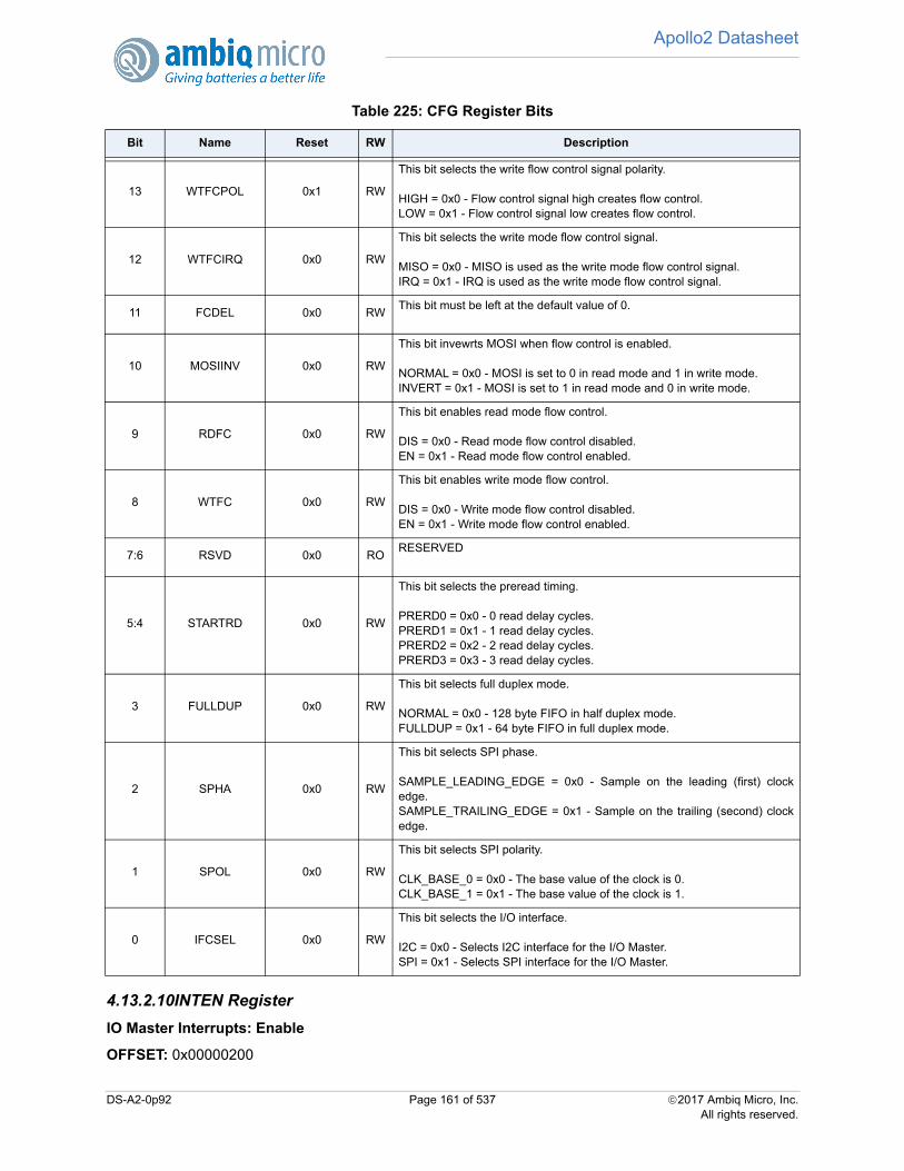
Apollo2 Datasheet
4.13.2.10INTEN Register
IO Master Interrupts: Enable
OFFSET: 0x00000200
13 WTFCPOL 0x1 RW
This bit selects the write flow control signal polarity.
HIGH = 0x0 - Flow control signal high creates flow control.LOW = 0x1 - Flow control signal low creates flow control.
12 WTFCIRQ 0x0 RW
This bit selects the write mode flow control signal.
MISO = 0x0 - MISO is used as the write mode flow control signal.IRQ = 0x1 - IRQ is used as the write mode flow control signal.
11 FCDEL 0x0 RWThis bit must be left at the default value of 0.
10 MOSIINV 0x0 RW
This bit invewrts MOSI when flow control is enabled.
NORMAL = 0x0 - MOSI is set to 0 in read mode and 1 in write mode.INVERT = 0x1 - MOSI is set to 1 in read mode and 0 in write mode.
9 RDFC 0x0 RW
This bit enables read mode flow control.
DIS = 0x0 - Read mode flow control disabled.EN = 0x1 - Read mode flow control enabled.
8 WTFC 0x0 RW
This bit enables write mode flow control.
DIS = 0x0 - Write mode flow control disabled.EN = 0x1 - Write mode flow control enabled.
7:6 RSVD 0x0 RORESERVED
5:4 STARTRD 0x0 RW
This bit selects the preread timing.
PRERD0 = 0x0 - 0 read delay cycles.PRERD1 = 0x1 - 1 read delay cycles.PRERD2 = 0x2 - 2 read delay cycles.PRERD3 = 0x3 - 3 read delay cycles.
3 FULLDUP 0x0 RW
This bit selects full duplex mode.
NORMAL = 0x0 - 128 byte FIFO in half duplex mode.FULLDUP = 0x1 - 64 byte FIFO in full duplex mode.
2 SPHA 0x0 RW
This bit selects SPI phase.
SAMPLE_LEADING_EDGE = 0x0 - Sample on the leading (first) clockedge.SAMPLE_TRAILING_EDGE = 0x1 - Sample on the trailing (second) clockedge.
1 SPOL 0x0 RW
This bit selects SPI polarity.
CLK_BASE_0 = 0x0 - The base value of the clock is 0.CLK_BASE_1 = 0x1 - The base value of the clock is 1.
0 IFCSEL 0x0 RW
This bit selects the I/O interface.
I2C = 0x0 - Selects I2C interface for the I/O Master.SPI = 0x1 - Selects SPI interface for the I/O Master.
Table 225: CFG Register Bits
Bit Name Reset RW Description
DS-A2-0p92 Page 161 of 537 2017 Ambiq Micro, Inc.All rights reserved.
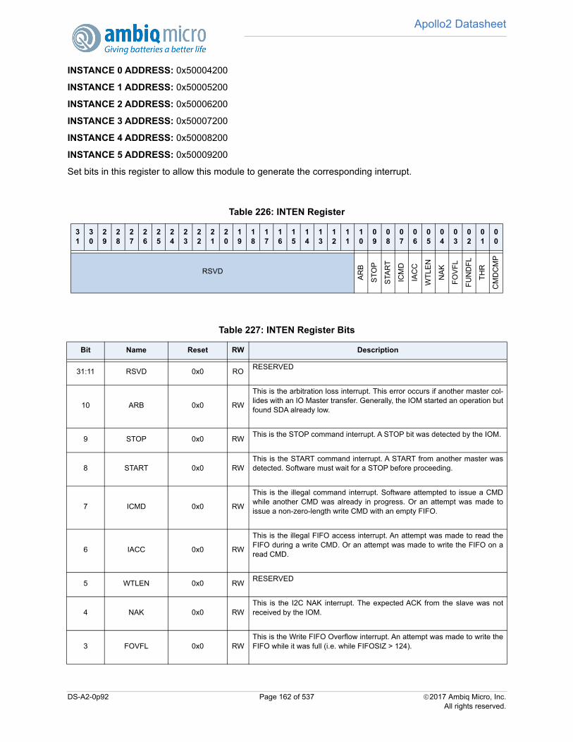
Apollo2 Datasheet
INSTANCE 0 ADDRESS: 0x50004200
INSTANCE 1 ADDRESS: 0x50005200
INSTANCE 2 ADDRESS: 0x50006200
INSTANCE 3 ADDRESS: 0x50007200
INSTANCE 4 ADDRESS: 0x50008200
INSTANCE 5 ADDRESS: 0x50009200
Set bits in this register to allow this module to generate the corresponding interrupt.
Table 226: INTEN Register
31
30
29
28
27
26
25
24
23
22
21
20
19
18
17
16
15
14
13
12
11
10
09
08
07
06
05
04
03
02
01
00
RSVD
AR
B
ST
OP
STA
RT
ICM
D
IAC
C
WT
LE
N
NA
K
FO
VF
L
FU
ND
FL
TH
R
CM
DC
MP
Table 227: INTEN Register Bits
Bit Name Reset RW Description
31:11 RSVD 0x0 RORESERVED
10 ARB 0x0 RW
This is the arbitration loss interrupt. This error occurs if another master col-lides with an IO Master transfer. Generally, the IOM started an operation butfound SDA already low.
9 STOP 0x0 RWThis is the STOP command interrupt. A STOP bit was detected by the IOM.
8 START 0x0 RWThis is the START command interrupt. A START from another master wasdetected. Software must wait for a STOP before proceeding.
7 ICMD 0x0 RW
This is the illegal command interrupt. Software attempted to issue a CMDwhile another CMD was already in progress. Or an attempt was made toissue a non-zero-length write CMD with an empty FIFO.
6 IACC 0x0 RW
This is the illegal FIFO access interrupt. An attempt was made to read theFIFO during a write CMD. Or an attempt was made to write the FIFO on aread CMD.
5 WTLEN 0x0 RWRESERVED
4 NAK 0x0 RWThis is the I2C NAK interrupt. The expected ACK from the slave was notreceived by the IOM.
3 FOVFL 0x0 RWThis is the Write FIFO Overflow interrupt. An attempt was made to write theFIFO while it was full (i.e. while FIFOSIZ > 124).
DS-A2-0p92 Page 162 of 537 2017 Ambiq Micro, Inc.All rights reserved.
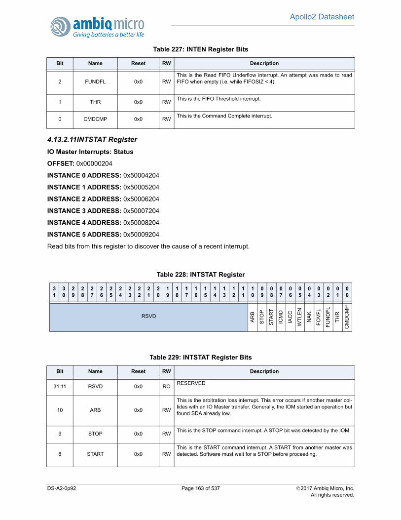
Apollo2 Datasheet
4.13.2.11INTSTAT Register
IO Master Interrupts: Status
OFFSET: 0x00000204
INSTANCE 0 ADDRESS: 0x50004204
INSTANCE 1 ADDRESS: 0x50005204
INSTANCE 2 ADDRESS: 0x50006204
INSTANCE 3 ADDRESS: 0x50007204
INSTANCE 4 ADDRESS: 0x50008204
INSTANCE 5 ADDRESS: 0x50009204
Read bits from this register to discover the cause of a recent interrupt.
2 FUNDFL 0x0 RWThis is the Read FIFO Underflow interrupt. An attempt was made to readFIFO when empty (i.e. while FIFOSIZ < 4).
1 THR 0x0 RWThis is the FIFO Threshold interrupt.
0 CMDCMP 0x0 RWThis is the Command Complete interrupt.
Table 228: INTSTAT Register
31
30
29
28
27
26
25
24
23
22
21
20
19
18
17
16
15
14
13
12
11
10
09
08
07
06
05
04
03
02
01
00
RSVD
AR
B
ST
OP
STA
RT
ICM
D
IAC
C
WT
LE
N
NA
K
FO
VF
L
FU
ND
FL
TH
R
CM
DC
MP
Table 229: INTSTAT Register Bits
Bit Name Reset RW Description
31:11 RSVD 0x0 RORESERVED
10 ARB 0x0 RW
This is the arbitration loss interrupt. This error occurs if another master col-lides with an IO Master transfer. Generally, the IOM started an operation butfound SDA already low.
9 STOP 0x0 RWThis is the STOP command interrupt. A STOP bit was detected by the IOM.
8 START 0x0 RWThis is the START command interrupt. A START from another master wasdetected. Software must wait for a STOP before proceeding.
Table 227: INTEN Register Bits
Bit Name Reset RW Description
DS-A2-0p92 Page 163 of 537 2017 Ambiq Micro, Inc.All rights reserved.

Apollo2 Datasheet
4.13.2.12INTCLR Register
IO Master Interrupts: Clear
OFFSET: 0x00000208
INSTANCE 0 ADDRESS: 0x50004208
INSTANCE 1 ADDRESS: 0x50005208
INSTANCE 2 ADDRESS: 0x50006208
INSTANCE 3 ADDRESS: 0x50007208
INSTANCE 4 ADDRESS: 0x50008208
INSTANCE 5 ADDRESS: 0x50009208
Write a 1 to a bit in this register to clear the interrupt status associated with that bit.
7 ICMD 0x0 RW
This is the illegal command interrupt. Software attempted to issue a CMDwhile another CMD was already in progress. Or an attempt was made toissue a non-zero-length write CMD with an empty FIFO.
6 IACC 0x0 RW
This is the illegal FIFO access interrupt. An attempt was made to read theFIFO during a write CMD. Or an attempt was made to write the FIFO on aread CMD.
5 WTLEN 0x0 RWRESERVED
4 NAK 0x0 RWThis is the I2C NAK interrupt. The expected ACK from the slave was notreceived by the IOM.
3 FOVFL 0x0 RWThis is the Write FIFO Overflow interrupt. An attempt was made to write theFIFO while it was full (i.e. while FIFOSIZ > 124).
2 FUNDFL 0x0 RWThis is the Read FIFO Underflow interrupt. An attempt was made to readFIFO when empty (i.e. while FIFOSIZ < 4).
1 THR 0x0 RWThis is the FIFO Threshold interrupt.
0 CMDCMP 0x0 RWThis is the Command Complete interrupt.
Table 230: INTCLR Register
31
30
29
28
27
26
25
24
23
22
21
20
19
18
17
16
15
14
13
12
11
10
09
08
07
06
05
04
03
02
01
00
RSVD
AR
B
ST
OP
STA
RT
ICM
D
IAC
C
WT
LE
N
NA
K
FO
VF
L
FU
ND
FL
TH
R
CM
DC
MP
Table 229: INTSTAT Register Bits
Bit Name Reset RW Description
DS-A2-0p92 Page 164 of 537 2017 Ambiq Micro, Inc.All rights reserved.

Apollo2 Datasheet
4.13.2.13INTSET Register
IO Master Interrupts: Set
OFFSET: 0x0000020C
INSTANCE 0 ADDRESS: 0x5000420C
INSTANCE 1 ADDRESS: 0x5000520C
INSTANCE 2 ADDRESS: 0x5000620C
INSTANCE 3 ADDRESS: 0x5000720C
INSTANCE 4 ADDRESS: 0x5000820C
INSTANCE 5 ADDRESS: 0x5000920C
Table 231: INTCLR Register Bits
Bit Name Reset RW Description
31:11 RSVD 0x0 RORESERVED
10 ARB 0x0 RW
This is the arbitration loss interrupt. This error occurs if another master col-lides with an IO Master transfer. Generally, the IOM started an operation butfound SDA already low.
9 STOP 0x0 RWThis is the STOP command interrupt. A STOP bit was detected by the IOM.
8 START 0x0 RWThis is the START command interrupt. A START from another master wasdetected. Software must wait for a STOP before proceeding.
7 ICMD 0x0 RW
This is the illegal command interrupt. Software attempted to issue a CMDwhile another CMD was already in progress. Or an attempt was made toissue a non-zero-length write CMD with an empty FIFO.
6 IACC 0x0 RW
This is the illegal FIFO access interrupt. An attempt was made to read theFIFO during a write CMD. Or an attempt was made to write the FIFO on aread CMD.
5 WTLEN 0x0 RWRESERVED
4 NAK 0x0 RWThis is the I2C NAK interrupt. The expected ACK from the slave was notreceived by the IOM.
3 FOVFL 0x0 RWThis is the Write FIFO Overflow interrupt. An attempt was made to write theFIFO while it was full (i.e. while FIFOSIZ > 124).
2 FUNDFL 0x0 RWThis is the Read FIFO Underflow interrupt. An attempt was made to readFIFO when empty (i.e. while FIFOSIZ < 4).
1 THR 0x0 RWThis is the FIFO Threshold interrupt.
0 CMDCMP 0x0 RWThis is the Command Complete interrupt.
DS-A2-0p92 Page 165 of 537 2017 Ambiq Micro, Inc.All rights reserved.

Apollo2 Datasheet
Write a 1 to a bit in this register to instantly generate an interrupt from this module. (Generally used fortesting purposes).
Table 232: INTSET Register
31
30
29
28
27
26
25
24
23
22
21
20
19
18
17
16
15
14
13
12
11
10
09
08
07
06
05
04
03
02
01
00
RSVD
AR
B
ST
OP
STA
RT
ICM
D
IAC
C
WT
LE
N
NA
K
FO
VF
L
FU
ND
FL
TH
R
CM
DC
MP
Table 233: INTSET Register Bits
Bit Name Reset RW Description
31:11 RSVD 0x0 RORESERVED
10 ARB 0x0 RW
This is the arbitration loss interrupt. This error occurs if another master col-lides with an IO Master transfer. Generally, the IOM started an operation butfound SDA already low.
9 STOP 0x0 RWThis is the STOP command interrupt. A STOP bit was detected by the IOM.
8 START 0x0 RWThis is the START command interrupt. A START from another master wasdetected. Software must wait for a STOP before proceeding.
7 ICMD 0x0 RW
This is the illegal command interrupt. Software attempted to issue a CMDwhile another CMD was already in progress. Or an attempt was made toissue a non-zero-length write CMD with an empty FIFO.
6 IACC 0x0 RW
This is the illegal FIFO access interrupt. An attempt was made to read theFIFO during a write CMD. Or an attempt was made to write the FIFO on aread CMD.
5 WTLEN 0x0 RWRESERVED
4 NAK 0x0 RWThis is the I2C NAK interrupt. The expected ACK from the slave was notreceived by the IOM.
3 FOVFL 0x0 RWThis is the Write FIFO Overflow interrupt. An attempt was made to write theFIFO while it was full (i.e. while FIFOSIZ > 124).
2 FUNDFL 0x0 RWThis is the Read FIFO Underflow interrupt. An attempt was made to readFIFO when empty (i.e. while FIFOSIZ < 4).
1 THR 0x0 RWThis is the FIFO Threshold interrupt.
0 CMDCMP 0x0 RWThis is the Command Complete interrupt.
DS-A2-0p92 Page 166 of 537 2017 Ambiq Micro, Inc.All rights reserved.

Apollo2 Datasheet
DS-A2-0p92 Page 167 of 537 2017 Ambiq Micro, Inc.All rights reserved.

Apollo2 Datasheet
5. I2C/SPI Slave Module
Figure 30. Block diagram for the I2C/SPI Slave Module
5.1 Functional Overview
The I2C/SPI Slave Module, shown in Figure , allows the Apollo2 MCU to function as a Slave in an I2C or
SPI system. The I2C/SPI Slave operates in an independent fashion, so that the Apollo2 MCU may beplaced into a sleep mode and still receive operations over the I/O interface. The Slave may be configuredto generate an interrupt on specific references.
The I2C/SPI Slave contains 256 bytes of RAM which is only accessible when the module is enabled. ThisRAM may be flexibly configured into three spaces: a block directly accessible via the I/O interface, a blockwhich functions as a FIFO for read operations on the interface, and a block of generally accessible RAMused to store parameters during deep sleep mode.
In I2C mode the Slave supports fully configurable 7 and 10-bit addressing with interface timing limits asspecified in Table 781. In SPI mode, the Slave supports all polarity/phase combinations and interfacefrequencies as specified in Table 784.
5.2 Local RAM Allocation
The I2C/SPI Slave is built around a 256-byte local RAM (LRAM), through which all data flows between the
CPU AHB and the IO interface. The I2C/SPI Slave supports a 128-byte offset space when accessed fromthe I/O interface.
The LRAM is divided into three separate areas on 8-byte boundaries. These areas are:
I2C/SPI Interface
To PinsIOSM
LRAM
Bus InterfaceREQs
STALL
REQs
Regs
Counters, Pointers
ADDR, WDATA
RDATA
ADDR, WDATA
RDATA
IOINT
IOCLK
DS-A2-0p92 Page 168 of 537 2017 Ambiq Micro, Inc.All rights reserved.
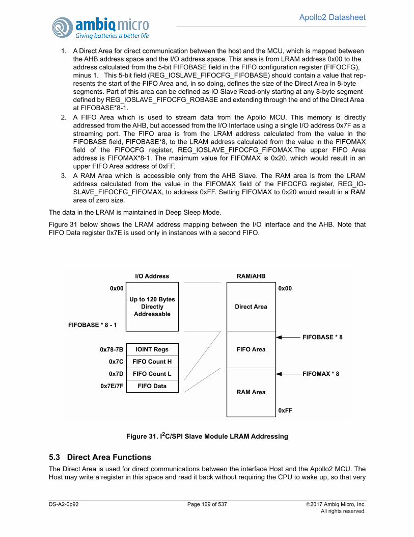
Apollo2 Datasheet
1. A Direct Area for direct communication between the host and the MCU, which is mapped between the AHB address space and the I/O address space. This area is from LRAM address 0x00 to the address calculated from the 5-bit FIFOBASE field in the FIFO configuration register (FIFOCFG), minus 1. This 5-bit field (REG_IOSLAVE_FIFOCFG_FIFOBASE) should contain a value that rep-resents the start of the FIFO Area and, in so doing, defines the size of the Direct Area in 8-byte segments. Part of this area can be defined as IO Slave Read-only starting at any 8-byte segment defined by REG_IOSLAVE_FIFOCFG_ROBASE and extending through the end of the Direct Area at FIFOBASE*8-1.
2. A FIFO Area which is used to stream data from the Apollo MCU. This memory is directlyaddressed from the AHB, but accessed from the I/O Interface using a single I/O address 0x7F as astreaming port. The FIFO area is from the LRAM address calculated from the value in theFIFOBASE field, FIFOBASE*8, to the LRAM address calculated from the value in the FIFOMAXfield of the FIFOCFG register, REG_IOSLAVE_FIFOCFG_FIFOMAX.The upper FIFO Areaaddress is FIFOMAX*8-1. The maximum value for FIFOMAX is 0x20, which would result in anupper FIFO Area address of 0xFF.
3. A RAM Area which is accessible only from the AHB Slave. The RAM area is from the LRAMaddress calculated from the value in the FIFOMAX field of the FIFOCFG register, REG_IO-SLAVE_FIFOCFG_FIFOMAX, to address 0xFF. Setting FIFOMAX to 0x20 would result in a RAMarea of zero size.
The data in the LRAM is maintained in Deep Sleep Mode.
Figure 31 below shows the LRAM address mapping between the I/O interface and the AHB. Note thatFIFO Data register 0x7E is used only in instances with a second FIFO.
Figure 31. I2C/SPI Slave Module LRAM Addressing
5.3 Direct Area FunctionsThe Direct Area is used for direct communications between the interface Host and the Apollo2 MCU. TheHost may write a register in this space and read it back without requiring the CPU to wake up, so that very
Up to 120 Bytes Directly
Addressable
FIFO Data
0x00
0x7E/7F
I/O Address
FIFO Count H0x7C
FIFO Count L
Direct Area
RAM/AHB
0x00
FIFO Area
RAM Area
0x7D
0xFF
IOINT Regs
FIFOBASE * 8
FIFOMAX * 8
FIFOBASE * 8 - 1
0x78-7B
DS-A2-0p92 Page 169 of 537 2017 Ambiq Micro, Inc.All rights reserved.

Apollo2 Datasheet
low power interactions are supported. In most cases, however, some accesses require interaction with theCPU, so the Direct Area is further divided into three areas for CPU interaction.
I/O writes to locations 0x0-0xF will set a corresponding interrupt flag in the REGACCINTSTAT register.These locations are typically used for specific commands to the Apollo2 MCU. Note that not all flags needgenerate an actual interrupt, so small multi-byte commands may be transmitted in this area. For example,a write to location 0x0 will set bit 31 of the REGACCINTSTAT register, a write to location 0x1 will set bit 30of REGACCINTSTAT, and a write to location 0xF will set bit 16 of the REGACCINTSTAT register.
I/O writes to locations 0x10 to 0x4F will set a corresponding interrupt flag in the REGACCINTSTAT registerif the I/O address modulo 4 is 3 (i.e. addresses 0x13, 0x17, 0x1B, etc.). This allows larger transfers to besent in a burst with a trigger being generated on the last write, and it also allows specifying a data buffer ofany whole word size and have an interrupt generated on access to the last byte of the buffer. Forexample, a write to location 0x13 will set bit 15 of the REGACCINTSTAT register, a write to location 0x17will set bit 14 of REGACCINTSTAT, and a write to location 0x4F will set bit 0 of the REGACCINTSTATregister.
Table 234 lists the offsets to memory locations within the Direct Address Space and correspondinginterrupt bit settings in the REGACCINTSTAT register.
DS-A2-0p92 Page 170 of 537 2017 Ambiq Micro, Inc.All rights reserved.
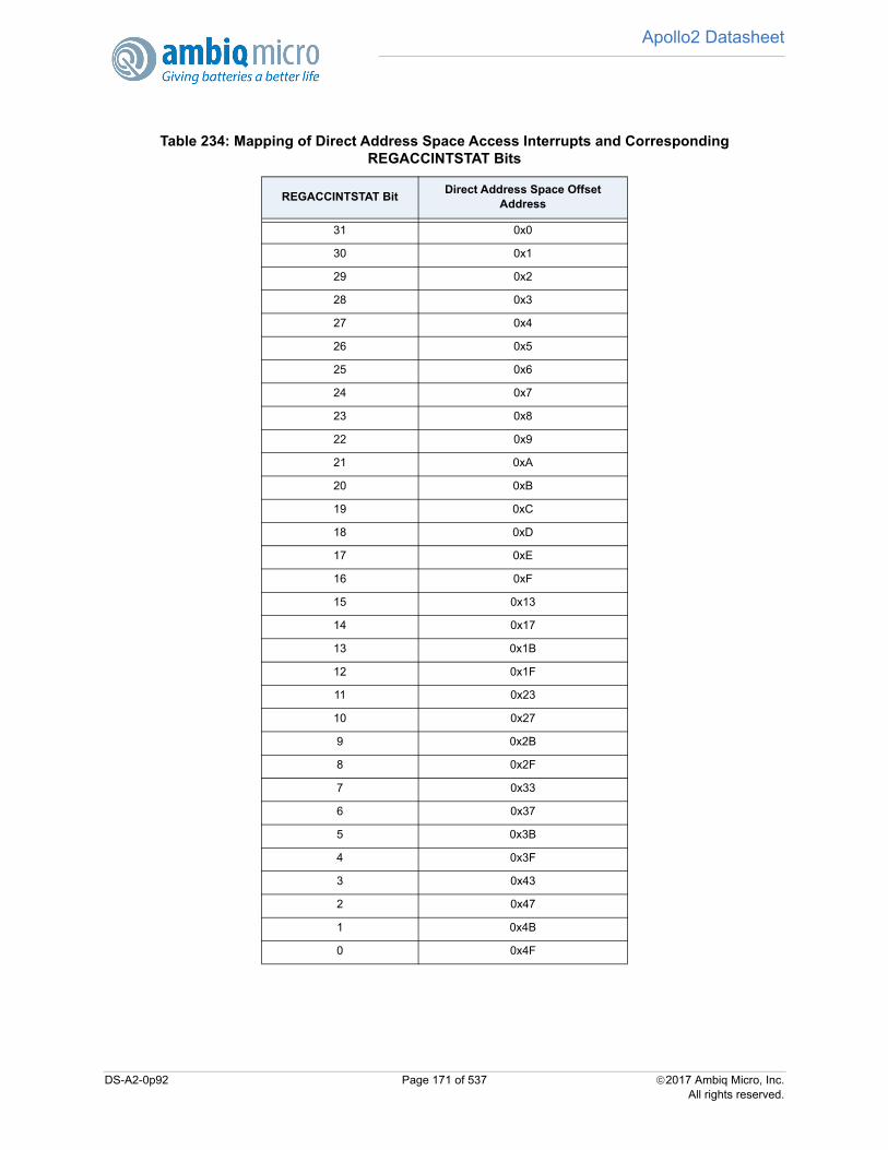
Apollo2 Datasheet
Table 234: Mapping of Direct Address Space Access Interrupts and Corresponding REGACCINTSTAT Bits
REGACCINTSTAT BitDirect Address Space Offset
Address
31 0x0
30 0x1
29 0x2
28 0x3
27 0x4
26 0x5
25 0x6
24 0x7
23 0x8
22 0x9
21 0xA
20 0xB
19 0xC
18 0xD
17 0xE
16 0xF
15 0x13
14 0x17
13 0x1B
12 0x1F
11 0x23
10 0x27
9 0x2B
8 0x2F
7 0x33
6 0x37
5 0x3B
4 0x3F
3 0x43
2 0x47
1 0x4B
0 0x4F
DS-A2-0p92 Page 171 of 537 2017 Ambiq Micro, Inc.All rights reserved.
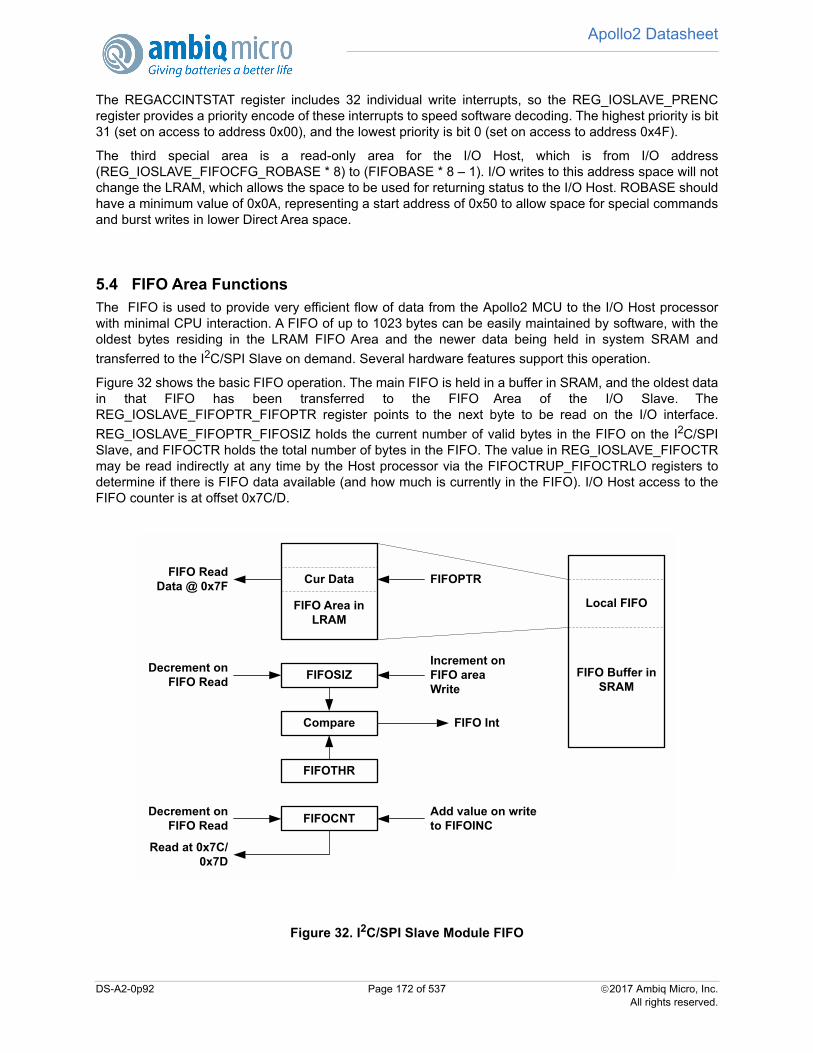
Apollo2 Datasheet
The REGACCINTSTAT register includes 32 individual write interrupts, so the REG_IOSLAVE_PRENCregister provides a priority encode of these interrupts to speed software decoding. The highest priority is bit31 (set on access to address 0x00), and the lowest priority is bit 0 (set on access to address 0x4F).
The third special area is a read-only area for the I/O Host, which is from I/O address(REG_IOSLAVE_FIFOCFG_ROBASE * 8) to (FIFOBASE * 8 – 1). I/O writes to this address space will notchange the LRAM, which allows the space to be used for returning status to the I/O Host. ROBASE shouldhave a minimum value of 0x0A, representing a start address of 0x50 to allow space for special commandsand burst writes in lower Direct Area space.
5.4 FIFO Area FunctionsThe FIFO is used to provide very efficient flow of data from the Apollo2 MCU to the I/O Host processorwith minimal CPU interaction. A FIFO of up to 1023 bytes can be easily maintained by software, with theoldest bytes residing in the LRAM FIFO Area and the newer data being held in system SRAM and
transferred to the I2C/SPI Slave on demand. Several hardware features support this operation.
Figure 32 shows the basic FIFO operation. The main FIFO is held in a buffer in SRAM, and the oldest datain that FIFO has been transferred to the FIFO Area of the I/O Slave. TheREG_IOSLAVE_FIFOPTR_FIFOPTR register points to the next byte to be read on the I/O interface.
REG_IOSLAVE_FIFOPTR_FIFOSIZ holds the current number of valid bytes in the FIFO on the I2C/SPISlave, and FIFOCTR holds the total number of bytes in the FIFO. The value in REG_IOSLAVE_FIFOCTRmay be read indirectly at any time by the Host processor via the FIFOCTRUP_FIFOCTRLO registers todetermine if there is FIFO data available (and how much is currently in the FIFO). I/O Host access to theFIFO counter is at offset 0x7C/D.
Figure 32. I2C/SPI Slave Module FIFO
FIFO Buffer in SRAM
Local FIFOFIFO Area in LRAM
FIFOPTRCur DataFIFO Read Data @ 0x7F
FIFOSIZ
FIFOTHR
Compare FIFO Int
Decrement on FIFO Read
Increment on FIFO area Write
FIFOCNTDecrement on FIFO Read
Add value on write to FIFOINC
Read at 0x7C/0x7D
DS-A2-0p92 Page 172 of 537 2017 Ambiq Micro, Inc.All rights reserved.
Apollo2 Datasheet
When the host reads a byte from the FIFO, the data retrieved is pointed to by FIFOPTR, FIFOPTR isincremented and wraps around in the FIFO Area if it reaches FIFOMAX. FIFOSIZ and FIFOCTR are eachdecremented by one. The Host can read FIFOCTR and then read that many bytes without furtherchecking. Note that this process can continue without requiring a CPU wakeup. If the Host attempts to read
the FIFO when FIFOSIZ is 0, the FUNDFL interrupt flag is set in both the I2C Slave interrupt block and inthe Host interrupt block.
When FIFOSIZ drops below the configured threshold REG_IOSLAVE_FIFOTHR the FSIZE interrupt flag isset and if enabled an interrupt is sent to the CPU which will wake it up. At that point, the CPU can move as
much data from the SRAM FIFO to the I2C/SPI Slave FIFO as possible in a single operation and then goback to sleep. Since the FIFO Area can be quite large, CPU wake-ups will be very infrequent. If a write tothe FIFOCTR which would increment the value beyond 1023 occurs, the FOVFL interrupt flag is set.
When some other process, such as a sensor read, produces new data for the FIFO, the CPU will add thatdata to the FIFO in SRAM, wrapping around as necessary. The REG_IOSLAVE_FIFOINC register is thenwritten with the number of bytes added to the FIFO, which is added to the FIFOCTR register in an atomicfashion. In this way the Host processor can always determine how much read data is available.
The FIFO interface offset 0x7F is treated uniquely by the I2C/SPI Slave, in that an access to this addressdoes not increment the Address Pointer. This allows the Host to initiate a burst read from address 0x7F ofany length, and each read will supply the next byte in the FIFO.
5.5 Rearranging the FIFOIn normal operation the Host reads the oldest data from the FIFO, and the CPU writes new data onto theFIFO. In some cases it is desirable to modify this process, in particular for the FIFO to provide the newestdata. The Apollo2 MCU supports such operation using a special control function.
If software desires to write the current sample to the front of the FIFO, it first checks theREG_IOSLAVE_FUPD_IOREAD status bit to ensure that there is not a Host read operation from the FIFOunderway. Once IOREAD is clear, software sets the REG_IOSLAVE_FUPD_FIFOUPD bit, writes the newsample data to the front of the FIFO and modifies the FIFOPTR to point to the new data. At that point theFIFOUPD bit is cleared.
If the Host attempts a FIFO read operation while the FIFOUPD is set, a RDERR interrupt will be generatedto the Host and the FRDERR interrupt flag will be set. The Host must either poll the RDERR interrupt bit atthe end of each operation or configure a hardware interrupt. Note that if the software does not supportalternate FIFO ordering, the Host does not have to check the RDERR function.
5.6 Interface InterruptsThe CPU may also signal the Host via the IOINT interrupt, which may be connected to an Apollo2 MCU pinand driven to the Host. Eight interrupts are available to be combined into the IOINT interrupt, and the Hostcan enable, read, clear and set these interrupts via the I/O interface. Software on the CPU can set 6 of theinterrupts (SWINT0 through SWINT5) to communicate a variety of situations to the Host, and the other twointerrupts indicate errors such as an attempt by the Host to read the FIFO when it is empty. A CPU interruptis generated whenever the Host writes any IOINT registers (for example, to clear an interrupt) so the CPUcan manage the interrupt interaction.The I2C/SPI Slave includes a mechanism to allow the Host CPU andthe Apollo2 MCU to each interrupt the other via a set of eight interrupts. The Host CPU accesses theseinterrupts via interface locations 0x78-0x7B, and the Apollo2 MCU accesses these interrupts in theIOINTCTL Register.
The Host CPU may enable or disable any of the eight interrupts by writing the corresponding bit in theIOINTEN field of the IOINTCTL Register, which is accessed by the Host at interface location 0x78. TheHost CPU may then clear or set any of the interrupts by writing a 1 to the corresponding bit of the clear (atlocation 0x7A) or set (at location 0x7B) registers. The current state of all eight interrupts may be read in the
DS-A2-0p92 Page 173 of 537 2017 Ambiq Micro, Inc.All rights reserved.

Apollo2 Datasheet
IOINT field at location 0x79. Note that this structure is identical to the standard Apollo2 MCU interrupts inall modules. The Apollo2 MCU can read the value of the eight interrupt enables in the IOINTEN field ofIOINTCTL, and can read the values of the eight interrupt status bits in the IOINT field of the IOINTCTLregister. These two fields are read only. Table 235 summarizes these I/O interface interrupts and how theycan be controlled and read.
The Apollo2 MCU software may set any of the eight interrupt status register bits by writing a 1 to thecorresponding bit of the IOINTSET field of the IOINTCTL Register, and may clear all of the interrupts bywriting a 1 to the IOINTCLR bit of the IOINTCTL register. This allows the Apollo2 MCU to generate asoftware interrupt to the Host device. In addition, a FIFO underflow interrupt FUNDFL in the I2C/SPI Slavewill set interrupt bit 7, and a FIFO read error interrupt FRDERR will set interrupt bit 6 of the IO interruptstatus register IOINT. Note that the Apollo2 MCU software cannot write the IOINTEN register, so that IOinterrupts are controlled completely by the Host processor.
If any of the IOINT interrupt bits are set and the corresponding bit in IOINTEN is set, an IOINT interrupt willbe generated. If the GPIO configuration registers have configured PAD4 as IOINT, that interrupt will bedriven directly onto PAD_IO[4]. This pin should be connected to an interrupt input pin of the Host interfacedevice so that it can receive the interrupt and service it.
If the Host device writes to any of the interrupt register access locations (any location in 0x78-0x7B) theIOINTW interrupt will be set in the I2C/SPI INTSTAT Register. This allows Apollo2 MCU software to receivea software interrupt from the Host device. Note that this interrupt will occur for all writes by the Host,including a write to clear an interrupt.
5.7 Command Completion InterruptsFour interrupts in the I2C/SPI Slave module are generated when the Host interface device completes atransfer. This allows Apollo2 MCU to be easily awakened for any transfer from the Host while maximizingthe time Apollo2 MCU is in sleep mode. The XCMPWR interrupt is generated at the completion of a Hostwrite transfer which includes addresses in the currently configured Direct Register space, and theXCMPRR interrupt is generated on the completion of a Host read transfer to that space. The XCMPWFinterrupt is generated at the completion of a Host write transfer which includes the FIFO address 0xFF(although that is an invalid access), and the XCMPRF interrupt is generated at the completion of a Hostread transfer which includes the FIFO address 0xFF. Note that a burst transfer which begins in the DirectRegister address space and is long enough to cause the Address Pointer to be 0xFF can set both theDirect Register and FIFO interrupts, although that would in general be an invalid operation.
Table 235: I/O Interface Interrupt Control
RAM Location
IOINT
Register1
1. Readable by the I/O Host
Function MCU Register_Field Description
0x78 IOINTENI/O Interrupt Enable
IOINTCTL_IOINTEN (R/O)Each interrupt can be individually enabled by I/OHost, but can only be read by the MCU
0x79 IOINT I/O Interrupt State IOINTCTL_IOINT (R/O)State of each interrupt, set or cleared, can beread by either the I/O Host or by the MCU
0x7A IOINTCLR I/O Interrupt Clear IOINTCTL_IOINTCLR (W/OEach interrupt can be individually cleared by theI/O Host, but the MCU can (only) clear all ofthem at once
0x7B IOINTSET I/O Interrupt SetIOINTCTL_IOINTSET (W/O)
Each interrupt can be individually set by eitherthe I/O Host or the MCU
DS-A2-0p92 Page 174 of 537 2017 Ambiq Micro, Inc.All rights reserved.
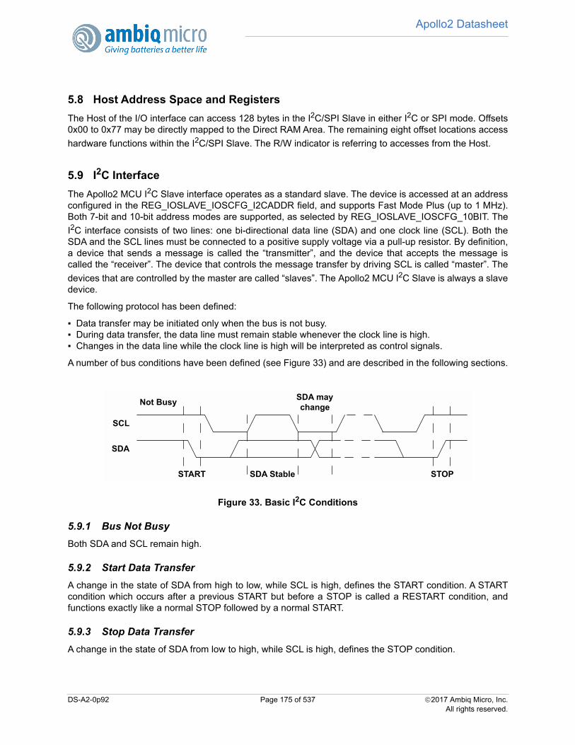
Apollo2 Datasheet
5.8 Host Address Space and Registers
The Host of the I/O interface can access 128 bytes in the I2C/SPI Slave in either I2C or SPI mode. Offsets0x00 to 0x77 may be directly mapped to the Direct RAM Area. The remaining eight offset locations access
hardware functions within the I2C/SPI Slave. The R/W indicator is referring to accesses from the Host.
5.9 I2C Interface
The Apollo2 MCU I2C Slave interface operates as a standard slave. The device is accessed at an addressconfigured in the REG_IOSLAVE_IOSCFG_I2CADDR field, and supports Fast Mode Plus (up to 1 MHz).Both 7-bit and 10-bit address modes are supported, as selected by REG_IOSLAVE_IOSCFG_10BIT. The
I2C interface consists of two lines: one bi-directional data line (SDA) and one clock line (SCL). Both theSDA and the SCL lines must be connected to a positive supply voltage via a pull-up resistor. By definition,a device that sends a message is called the “transmitter”, and the device that accepts the message iscalled the “receiver”. The device that controls the message transfer by driving SCL is called “master”. The
devices that are controlled by the master are called “slaves”. The Apollo2 MCU I2C Slave is always a slavedevice.
The following protocol has been defined:
Data transfer may be initiated only when the bus is not busy. During data transfer, the data line must remain stable whenever the clock line is high. Changes in the data line while the clock line is high will be interpreted as control signals.
A number of bus conditions have been defined (see Figure 33) and are described in the following sections.
Figure 33. Basic I2C Conditions
5.9.1 Bus Not Busy
Both SDA and SCL remain high.
5.9.2 Start Data Transfer
A change in the state of SDA from high to low, while SCL is high, defines the START condition. A STARTcondition which occurs after a previous START but before a STOP is called a RESTART condition, andfunctions exactly like a normal STOP followed by a normal START.
5.9.3 Stop Data Transfer
A change in the state of SDA from low to high, while SCL is high, defines the STOP condition.
SDA
SCL
START SDA Stable
SDA may change
STOP
Not Busy
DS-A2-0p92 Page 175 of 537 2017 Ambiq Micro, Inc.All rights reserved.
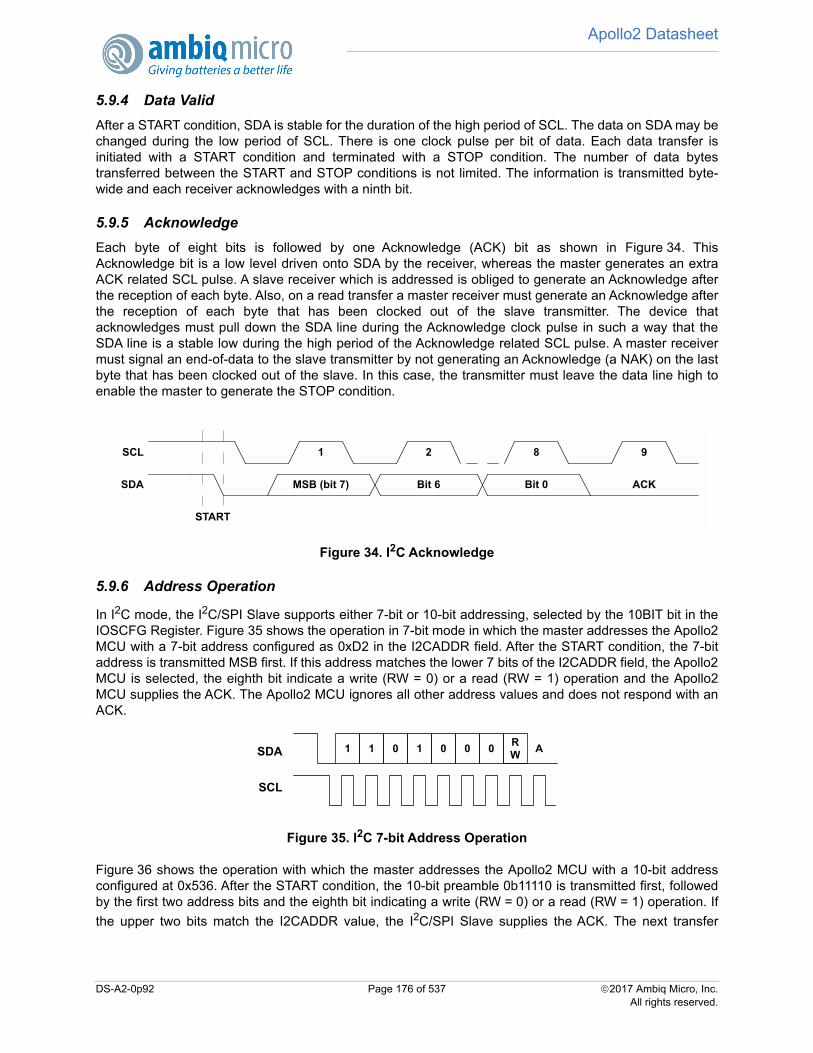
Apollo2 Datasheet
5.9.4 Data Valid
After a START condition, SDA is stable for the duration of the high period of SCL. The data on SDA may bechanged during the low period of SCL. There is one clock pulse per bit of data. Each data transfer isinitiated with a START condition and terminated with a STOP condition. The number of data bytestransferred between the START and STOP conditions is not limited. The information is transmitted byte-wide and each receiver acknowledges with a ninth bit.
5.9.5 Acknowledge
Each byte of eight bits is followed by one Acknowledge (ACK) bit as shown in Figure 34. ThisAcknowledge bit is a low level driven onto SDA by the receiver, whereas the master generates an extraACK related SCL pulse. A slave receiver which is addressed is obliged to generate an Acknowledge afterthe reception of each byte. Also, on a read transfer a master receiver must generate an Acknowledge afterthe reception of each byte that has been clocked out of the slave transmitter. The device thatacknowledges must pull down the SDA line during the Acknowledge clock pulse in such a way that theSDA line is a stable low during the high period of the Acknowledge related SCL pulse. A master receivermust signal an end-of-data to the slave transmitter by not generating an Acknowledge (a NAK) on the lastbyte that has been clocked out of the slave. In this case, the transmitter must leave the data line high toenable the master to generate the STOP condition.
Figure 34. I2C Acknowledge
5.9.6 Address Operation
In I2C mode, the I2C/SPI Slave supports either 7-bit or 10-bit addressing, selected by the 10BIT bit in theIOSCFG Register. Figure 35 shows the operation in 7-bit mode in which the master addresses the Apollo2MCU with a 7-bit address configured as 0xD2 in the I2CADDR field. After the START condition, the 7-bitaddress is transmitted MSB first. If this address matches the lower 7 bits of the I2CADDR field, the Apollo2MCU is selected, the eighth bit indicate a write (RW = 0) or a read (RW = 1) operation and the Apollo2MCU supplies the ACK. The Apollo2 MCU ignores all other address values and does not respond with anACK.
Figure 35. I2C 7-bit Address Operation
Figure 36 shows the operation with which the master addresses the Apollo2 MCU with a 10-bit addressconfigured at 0x536. After the START condition, the 10-bit preamble 0b11110 is transmitted first, followedby the first two address bits and the eighth bit indicating a write (RW = 0) or a read (RW = 1) operation. If
the upper two bits match the I2CADDR value, the I2C/SPI Slave supplies the ACK. The next transfer
SDA
SCL
START
MSB (bit 7) Bit 6 Bit 0 ACK
1 2 8 9
A1 1 0SDA
SCL
RW0 1 0 0
DS-A2-0p92 Page 176 of 537 2017 Ambiq Micro, Inc.All rights reserved.
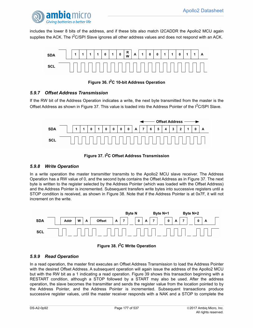
Apollo2 Datasheet
includes the lower 8 bits of the address, and if these bits also match I2CADDR the Apollo2 MCU again
supplies the ACK. The I2C/SPI Slave ignores all other address values and does not respond with an ACK.
Figure 36. I2C 10-bit Address Operation
5.9.7 Offset Address Transmission
If the RW bit of the Address Operation indicates a write, the next byte transmitted from the master is the
Offset Address as shown in Figure 37. This value is loaded into the Address Pointer of the I2C/SPI Slave.
Figure 37. I2C Offset Address Transmission
5.9.8 Write Operation
In a write operation the master transmitter transmits to the Apollo2 MCU slave receiver. The AddressOperation has a RW value of 0, and the second byte contains the Offset Address as in Figure 37. The nextbyte is written to the register selected by the Address Pointer (which was loaded with the Offset Address)and the Address Pointer is incremented. Subsequent transfers write bytes into successive registers until aSTOP condition is received, as shown in Figure 38. Note that if the Address Pointer is at 0x7F, it will notincrement on the write.
Figure 38. I2C Write Operation
5.9.9 Read Operation
In a read operation, the master first executes an Offset Address Transmission to load the Address Pointerwith the desired Offset Address. A subsequent operation will again issue the address of the Apollo2 MCUbut with the RW bit as a 1 indicating a read operation. Figure 39 shows this transaction beginning with aRESTART condition, although a STOP followed by a START may also be used. After the addressoperation, the slave becomes the transmitter and sends the register value from the location pointed to bythe Address Pointer, and the Address Pointer is incremented. Subsequent transactions producesuccessive register values, until the master receiver responds with a NAK and a STOP to complete the
A1 1 0SDA
SCL
RW A1 0 1 11 1 0 1 0 1 1 0
A1 1 0SDA
SCL
0 A7 6 1 0
Offset Address
0 1 0 0 5 4 3 2
Addr OffsetSDA
SCL
7 0
Byte N
AW A A 7 0
Byte N+1
A 7 0
Byte N+2
A
DS-A2-0p92 Page 177 of 537 2017 Ambiq Micro, Inc.All rights reserved.
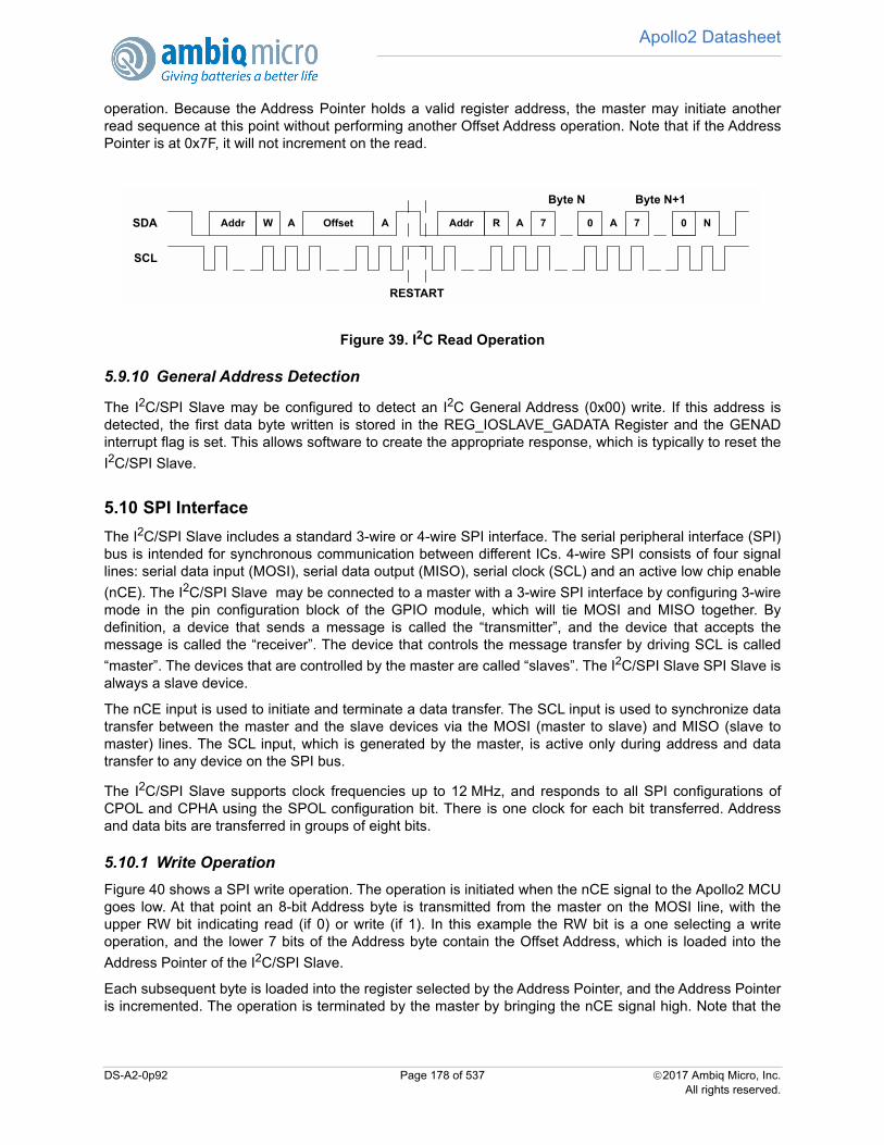
Apollo2 Datasheet
operation. Because the Address Pointer holds a valid register address, the master may initiate anotherread sequence at this point without performing another Offset Address operation. Note that if the AddressPointer is at 0x7F, it will not increment on the read.
Figure 39. I2C Read Operation
5.9.10 General Address Detection
The I2C/SPI Slave may be configured to detect an I2C General Address (0x00) write. If this address isdetected, the first data byte written is stored in the REG_IOSLAVE_GADATA Register and the GENADinterrupt flag is set. This allows software to create the appropriate response, which is typically to reset the
I2C/SPI Slave.
5.10 SPI Interface
The I2C/SPI Slave includes a standard 3-wire or 4-wire SPI interface. The serial peripheral interface (SPI)bus is intended for synchronous communication between different ICs. 4-wire SPI consists of four signallines: serial data input (MOSI), serial data output (MISO), serial clock (SCL) and an active low chip enable
(nCE). The I2C/SPI Slave may be connected to a master with a 3-wire SPI interface by configuring 3-wiremode in the pin configuration block of the GPIO module, which will tie MOSI and MISO together. Bydefinition, a device that sends a message is called the “transmitter”, and the device that accepts themessage is called the “receiver”. The device that controls the message transfer by driving SCL is called
“master”. The devices that are controlled by the master are called “slaves”. The I2C/SPI Slave SPI Slave isalways a slave device.
The nCE input is used to initiate and terminate a data transfer. The SCL input is used to synchronize datatransfer between the master and the slave devices via the MOSI (master to slave) and MISO (slave tomaster) lines. The SCL input, which is generated by the master, is active only during address and datatransfer to any device on the SPI bus.
The I2C/SPI Slave supports clock frequencies up to 12 MHz, and responds to all SPI configurations ofCPOL and CPHA using the SPOL configuration bit. There is one clock for each bit transferred. Addressand data bits are transferred in groups of eight bits.
5.10.1 Write Operation
Figure 40 shows a SPI write operation. The operation is initiated when the nCE signal to the Apollo2 MCUgoes low. At that point an 8-bit Address byte is transmitted from the master on the MOSI line, with theupper RW bit indicating read (if 0) or write (if 1). In this example the RW bit is a one selecting a writeoperation, and the lower 7 bits of the Address byte contain the Offset Address, which is loaded into the
Address Pointer of the I2C/SPI Slave.
Each subsequent byte is loaded into the register selected by the Address Pointer, and the Address Pointeris incremented. The operation is terminated by the master by bringing the nCE signal high. Note that the
SDA
SCL
7 0
Byte N
A A 7 0
Byte N+1
NAddr AR
RESTART
Addr OffsetAW
DS-A2-0p92 Page 178 of 537 2017 Ambiq Micro, Inc.All rights reserved.
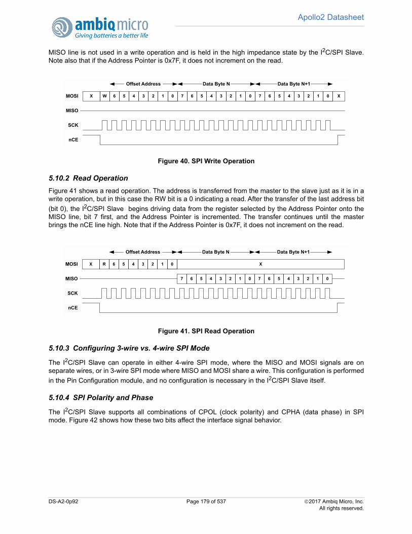
Apollo2 Datasheet
MISO line is not used in a write operation and is held in the high impedance state by the I2C/SPI Slave.Note also that if the Address Pointer is 0x7F, it does not increment on the read.
Figure 40. SPI Write Operation
5.10.2 Read Operation
Figure 41 shows a read operation. The address is transferred from the master to the slave just as it is in awrite operation, but in this case the RW bit is a 0 indicating a read. After the transfer of the last address bit
(bit 0), the I2C/SPI Slave begins driving data from the register selected by the Address Pointer onto theMISO line, bit 7 first, and the Address Pointer is incremented. The transfer continues until the masterbrings the nCE line high. Note that if the Address Pointer is 0x7F, it does not increment on the read.
Figure 41. SPI Read Operation
5.10.3 Configuring 3-wire vs. 4-wire SPI Mode
The I2C/SPI Slave can operate in either 4-wire SPI mode, where the MISO and MOSI signals are onseparate wires, or in 3-wire SPI mode where MISO and MOSI share a wire. This configuration is performed
in the Pin Configuration module, and no configuration is necessary in the I2C/SPI Slave itself.
5.10.4 SPI Polarity and Phase
The I2C/SPI Slave supports all combinations of CPOL (clock polarity) and CPHA (data phase) in SPImode. Figure 42 shows how these two bits affect the interface signal behavior.
W 6 1MOSI
SCK
0 7 6 1 0
Offset Address
nCE
X
Data Byte N
7 6 1 0
Data Byte N+1
X
MISO
5 4 3 2 5 4 3 2 5 4 3 2
R 6 1MOSI
SCK
0
Offset Address
nCE
X
Data Byte N Data Byte N+1
7 6 1 0 7 6 1 0MISO
X
5 4 3 2 5 4 3 2
5 4 3 2
DS-A2-0p92 Page 179 of 537 2017 Ambiq Micro, Inc.All rights reserved.
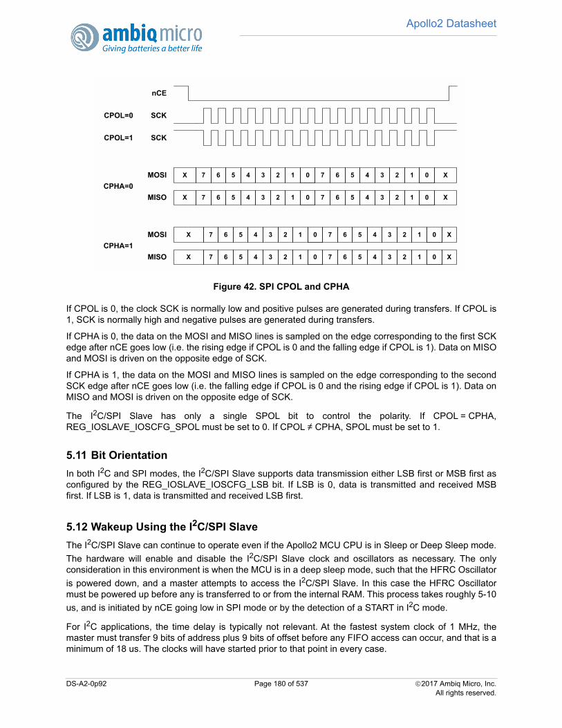
Apollo2 Datasheet
Figure 42. SPI CPOL and CPHA
If CPOL is 0, the clock SCK is normally low and positive pulses are generated during transfers. If CPOL is1, SCK is normally high and negative pulses are generated during transfers.
If CPHA is 0, the data on the MOSI and MISO lines is sampled on the edge corresponding to the first SCKedge after nCE goes low (i.e. the rising edge if CPOL is 0 and the falling edge if CPOL is 1). Data on MISOand MOSI is driven on the opposite edge of SCK.
If CPHA is 1, the data on the MOSI and MISO lines is sampled on the edge corresponding to the secondSCK edge after nCE goes low (i.e. the falling edge if CPOL is 0 and the rising edge if CPOL is 1). Data onMISO and MOSI is driven on the opposite edge of SCK.
The I2C/SPI Slave has only a single SPOL bit to control the polarity. If CPOL = CPHA,REG_IOSLAVE_IOSCFG_SPOL must be set to 0. If CPOL ≠ CPHA, SPOL must be set to 1.
5.11 Bit Orientation
In both I2C and SPI modes, the I2C/SPI Slave supports data transmission either LSB first or MSB first asconfigured by the REG_IOSLAVE_IOSCFG_LSB bit. If LSB is 0, data is transmitted and received MSBfirst. If LSB is 1, data is transmitted and received LSB first.
5.12 Wakeup Using the I2C/SPI Slave
The I2C/SPI Slave can continue to operate even if the Apollo2 MCU CPU is in Sleep or Deep Sleep mode.
The hardware will enable and disable the I2C/SPI Slave clock and oscillators as necessary. The onlyconsideration in this environment is when the MCU is in a deep sleep mode, such that the HFRC Oscillator
is powered down, and a master attempts to access the I2C/SPI Slave. In this case the HFRC Oscillatormust be powered up before any is transferred to or from the internal RAM. This process takes roughly 5-10
us, and is initiated by nCE going low in SPI mode or by the detection of a START in I2C mode.
For I2C applications, the time delay is typically not relevant. At the fastest system clock of 1 MHz, themaster must transfer 9 bits of address plus 9 bits of offset before any FIFO access can occur, and that is aminimum of 18 us. The clocks will have started prior to that point in every case.
CPOL=0
CPOL=1
7 6 1MOSI 0 7 6 1 0X 5 4 3 2 5 4 3 2
7 6 1MISO 0 7 6 1 0X 5 4 3 2 5 4 3 2
SCK
7 6 1MOSI 0 7 6 1 0X 5 4 3 2 5 4 3 2
7 6 1MISO 0 7 6 1 0X 5 4 3 2 5 4 3 2
CPHA=0
CPHA=1
X
X
X
X
SCK
nCE
DS-A2-0p92 Page 180 of 537 2017 Ambiq Micro, Inc.All rights reserved.
Apollo2 Datasheet
For SPI applications with fast interface clocks (faster than 1 MHz), the master must be programmed to pullnCE low at least 10 us prior to sending the first clock. If a master is unable to control the timing of nCE inthis way, then a GPIO interrupt can be configured to wake the Apollo2 MCU prior to initiating any SPItransfers.
There is no delay restriction if the MCU is in normal Sleep mode. In that case the HFRC is not powered
down and the I2C/SPI Slave clock will start immediately when nCE goes low. Alternatively, the FRCHFRCbit may be set in the FRCHFRC Register in the CLK_GEN module. If this bit is set, the HFRC will continueto be active even if the Apollo2 MCU CPU is in deep sleep mode, so that the I2C/SPI Slave canimmediately begin transferring data independent of the SPI transfer rate. This will result in higher powerbecause the HFRC remains active, so the FRCHFRC bit should only be set if it is known that a transfer islikely to begin prior to another interrupt.
5.13 IOSLAVE RegistersI2C/SPI Slave
INSTANCE 0 BASE ADDRESS:0x50000000
5.13.1 Register Memory Map
Table 236: IOSLAVE Register Map
Address(s) Register Name Description
0x50000100 FIFOPTR Current FIFO Pointer
0x50000104 FIFOCFG FIFO Configuration
0x50000108 FIFOTHR FIFO Threshold Configuration
0x5000010C FUPD FIFO Update Status
0x50000110 FIFOCTR Overall FIFO Counter
0x50000114 FIFOINC Overall FIFO Counter Increment
0x50000118 CFG I/O Slave Configuration
0x5000011C PRENC I/O Slave Interrupt Priority Encode
0x50000120 IOINTCTL I/O Interrupt Control
0x50000124 GENADD General Address Data
0x50000200 INTEN IO Slave Interrupts: Enable
0x50000204 INTSTAT IO Slave Interrupts: Status
0x50000208 INTCLR IO Slave Interrupts: Clear
0x5000020C INTSET IO Slave Interrupts: Set
0x50000210 REGACCINTEN Register Access Interrupts: Enable
0x50000214 REGACCINTSTAT Register Access Interrupts: Status
0x50000218 REGACCINTCLR Register Access Interrupts: Clear
0x5000021C REGACCINTSET Register Access Interrupts: Set
DS-A2-0p92 Page 181 of 537 2017 Ambiq Micro, Inc.All rights reserved.

Apollo2 Datasheet
5.13.2 IOSLAVE Registers
5.13.2.1 FIFOPTR Register
Current FIFO Pointer
OFFSET: 0x00000100
INSTANCE 0 ADDRESS: 0x50000100
Current FIFO Pointer
5.13.2.2 FIFOCFG Register
FIFO Configuration
OFFSET: 0x00000104
INSTANCE 0 ADDRESS: 0x50000104
FIFO Configuration
Table 237: FIFOPTR Register
31
30
29
28
27
26
25
24
23
22
21
20
19
18
17
16
15
14
13
12
11
10
09
08
07
06
05
04
03
02
01
00
RSVD FIFOSIZ FIFOPTR
Table 238: FIFOPTR Register Bits
Bit Name Reset RW Description
31:16 RSVD 0x0 RORESERVED
15:8 FIFOSIZ 0x0 RWThe number of bytes currently in the hardware FIFO.
7:0 FIFOPTR 0x0 RWCurrent FIFO pointer.
Table 239: FIFOCFG Register
31
30
29
28
27
26
25
24
23
22
21
20
19
18
17
16
15
14
13
12
11
10
09
08
07
06
05
04
03
02
01
00
RS
VD
ROBASE RSVD
RS
VD
FIFOMAX RSVD FIFOBASE
DS-A2-0p92 Page 182 of 537 2017 Ambiq Micro, Inc.All rights reserved.

Apollo2 Datasheet
5.13.2.3 FIFOTHR Register
FIFO Threshold Configuration
OFFSET: 0x00000108
INSTANCE 0 ADDRESS: 0x50000108
FIFO Threshold Configuration
Table 240: FIFOCFG Register Bits
Bit Name Reset RW Description
31:30 RSVD 0x0 RORESERVED
29:24 ROBASE 0x20 RWDefines the read-only area. The IO Slave read-only area is situated inLRAM at (ROBASE*8) to (FIFOOBASE*8-1)
23:16 RSVD 0x0 RORESERVED
15:14 RSVD 0x0 RORESERVED
13:8 FIFOMAX 0x0 RW
These bits hold the maximum FIFO address in 8 byte segments. It is alsothe beginning of the RAM area of the LRAM. Note that no RAM area is con-figured if FIFOMAX is set to 0x1F.
7:5 RSVD 0x0 RORESERVED
4:0 FIFOBASE 0x0 RWThese bits hold the base address of the I/O FIFO in 8 byte segments.The IOSlave FIFO is situated in LRAM at (FIFOBASE*8) to (FIFOMAX*8-1).
Table 241: FIFOTHR Register
31
30
29
28
27
26
25
24
23
22
21
20
19
18
17
16
15
14
13
12
11
10
09
08
07
06
05
04
03
02
01
00
RSVD FIFOTHR
Table 242: FIFOTHR Register Bits
Bit Name Reset RW Description
31:8 RSVD 0x0 RORESERVED
7:0 FIFOTHR 0x0 RWFIFO size interrupt threshold.
DS-A2-0p92 Page 183 of 537 2017 Ambiq Micro, Inc.All rights reserved.
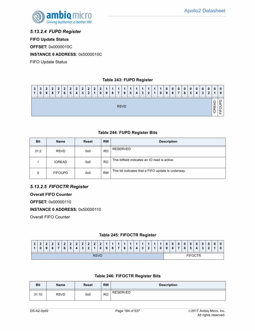
Apollo2 Datasheet
5.13.2.4 FUPD Register
FIFO Update Status
OFFSET: 0x0000010C
INSTANCE 0 ADDRESS: 0x5000010C
FIFO Update Status
5.13.2.5 FIFOCTR Register
Overall FIFO Counter
OFFSET: 0x00000110
INSTANCE 0 ADDRESS: 0x50000110
Overall FIFO Counter
Table 243: FUPD Register
31
30
29
28
27
26
25
24
23
22
21
20
19
18
17
16
15
14
13
12
11
10
09
08
07
06
05
04
03
02
01
00
RSVD
IOR
EA
D
FIF
OU
PD
Table 244: FUPD Register Bits
Bit Name Reset RW Description
31:2 RSVD 0x0 RORESERVED
1 IOREAD 0x0 ROThis bitfield indicates an IO read is active.
0 FIFOUPD 0x0 RWThis bit indicates that a FIFO update is underway.
Table 245: FIFOCTR Register
31
30
29
28
27
26
25
24
23
22
21
20
19
18
17
16
15
14
13
12
11
10
09
08
07
06
05
04
03
02
01
00
RSVD FIFOCTR
Table 246: FIFOCTR Register Bits
Bit Name Reset RW Description
31:10 RSVD 0x0 RORESERVED
DS-A2-0p92 Page 184 of 537 2017 Ambiq Micro, Inc.All rights reserved.

Apollo2 Datasheet
5.13.2.6 FIFOINC Register
Overall FIFO Counter Increment
OFFSET: 0x00000114
INSTANCE 0 ADDRESS: 0x50000114
Overall FIFO Counter Increment
5.13.2.7 CFG Register
I/O Slave Configuration
OFFSET: 0x00000118
INSTANCE 0 ADDRESS: 0x50000118
I/O Slave Configuration
9:0 FIFOCTR 0x0 RWVirtual FIFO byte count
Table 247: FIFOINC Register
31
30
29
28
27
26
25
24
23
22
21
20
19
18
17
16
15
14
13
12
11
10
09
08
07
06
05
04
03
02
01
00
RSVD FIFOINC
Table 248: FIFOINC Register Bits
Bit Name Reset RW Description
31:10 RSVD 0x0 RORESERVED
9:0 FIFOINC 0x0 WOIncrement the Overall FIFO Counter by this value on a write
Table 249: CFG Register
31
30
29
28
27
26
25
24
23
22
21
20
19
18
17
16
15
14
13
12
11
10
09
08
07
06
05
04
03
02
01
00
IFC
EN
RSVD I2CADDR RSVD
STA
RT
RD
RS
VD
LSB
SP
OL
IFC
SE
L
Table 246: FIFOCTR Register Bits
Bit Name Reset RW Description
DS-A2-0p92 Page 185 of 537 2017 Ambiq Micro, Inc.All rights reserved.

Apollo2 Datasheet
5.13.2.8 PRENC Register
I/O Slave Interrupt Priority Encode
OFFSET: 0x0000011C
INSTANCE 0 ADDRESS: 0x5000011C
I/O Slave Interrupt Priority Encode
Table 250: CFG Register Bits
Bit Name Reset RW Description
31 IFCEN 0x0 RW
IOSLAVE interface enable.
DIS = 0x0 - Disable the IOSLAVEEN = 0x1 - Enable the IOSLAVE
30:20 RSVD 0x0 RORESERVED
19:8 I2CADDR 0x0 RW7-bit or 10-bit I2C device address.
7:5 RSVD 0x0 RORESERVED
4 STARTRD 0x0 RW
This bit holds the cycle to initiate an I/O RAM read.
LATE = 0x0 - Initiate I/O RAM read late in each transferred byte.EARLY = 0x1 - Initiate I/O RAM read early in each transferred byte.
3 RSVD 0x0 RORESERVED
2 LSB 0x0 RW
This bit selects the transfer bit ordering.
MSB_FIRST = 0x0 - Data is assumed to be sent and received with MSBfirst.LSB_FIRST = 0x1 - Data is assumed to be sent and received with LSB first.
1 SPOL 0x0 RW
This bit selects SPI polarity.
SPI_MODES_0_3 = 0x0 - Polarity 0, handles SPI modes 0 and 3.SPI_MODES_1_2 = 0x1 - Polarity 1, handles SPI modes 1 and 2.
0 IFCSEL 0x0 RW
This bit selects the I/O interface.
I2C = 0x0 - Selects I2C interface for the IO Slave.SPI = 0x1 - Selects SPI interface for the IO Slave.
Table 251: PRENC Register
31
30
29
28
27
26
25
24
23
22
21
20
19
18
17
16
15
14
13
12
11
10
09
08
07
06
05
04
03
02
01
00
RSVD PRENC
DS-A2-0p92 Page 186 of 537 2017 Ambiq Micro, Inc.All rights reserved.
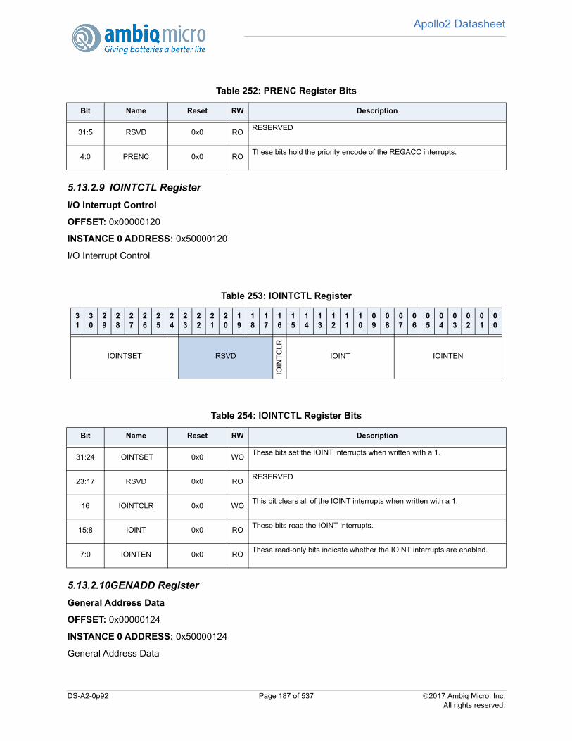
Apollo2 Datasheet
5.13.2.9 IOINTCTL Register
I/O Interrupt Control
OFFSET: 0x00000120
INSTANCE 0 ADDRESS: 0x50000120
I/O Interrupt Control
5.13.2.10GENADD Register
General Address Data
OFFSET: 0x00000124
INSTANCE 0 ADDRESS: 0x50000124
General Address Data
Table 252: PRENC Register Bits
Bit Name Reset RW Description
31:5 RSVD 0x0 RORESERVED
4:0 PRENC 0x0 ROThese bits hold the priority encode of the REGACC interrupts.
Table 253: IOINTCTL Register
31
30
29
28
27
26
25
24
23
22
21
20
19
18
17
16
15
14
13
12
11
10
09
08
07
06
05
04
03
02
01
00
IOINTSET RSVD
IOIN
TC
LR
IOINT IOINTEN
Table 254: IOINTCTL Register Bits
Bit Name Reset RW Description
31:24 IOINTSET 0x0 WOThese bits set the IOINT interrupts when written with a 1.
23:17 RSVD 0x0 RORESERVED
16 IOINTCLR 0x0 WOThis bit clears all of the IOINT interrupts when written with a 1.
15:8 IOINT 0x0 ROThese bits read the IOINT interrupts.
7:0 IOINTEN 0x0 ROThese read-only bits indicate whether the IOINT interrupts are enabled.
DS-A2-0p92 Page 187 of 537 2017 Ambiq Micro, Inc.All rights reserved.
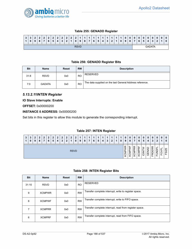
Apollo2 Datasheet
5.13.2.11INTEN Register
IO Slave Interrupts: Enable
OFFSET: 0x00000200
INSTANCE 0 ADDRESS: 0x50000200
Set bits in this register to allow this module to generate the corresponding interrupt.
Table 255: GENADD Register
31
30
29
28
27
26
25
24
23
22
21
20
19
18
17
16
15
14
13
12
11
10
09
08
07
06
05
04
03
02
01
00
RSVD GADATA
Table 256: GENADD Register Bits
Bit Name Reset RW Description
31:8 RSVD 0x0 RORESERVED
7:0 GADATA 0x0 ROThe data supplied on the last General Address reference.
Table 257: INTEN Register
31
30
29
28
27
26
25
24
23
22
21
20
19
18
17
16
15
14
13
12
11
10
09
08
07
06
05
04
03
02
01
00
RSVD
XC
MP
WR
XC
MP
WF
XC
MP
RR
XC
MP
RF
IOIN
TW
GE
NA
D
FR
DE
RR
FU
ND
FL
FO
VF
L
FS
IZE
Table 258: INTEN Register Bits
Bit Name Reset RW Description
31:10 RSVD 0x0 RORESERVED
9 XCMPWR 0x0 RWTransfer complete interrupt, write to register space.
8 XCMPWF 0x0 RWTransfer complete interrupt, write to FIFO space.
7 XCMPRR 0x0 RWTransfer complete interrupt, read from register space.
6 XCMPRF 0x0 RWTransfer complete interrupt, read from FIFO space.
DS-A2-0p92 Page 188 of 537 2017 Ambiq Micro, Inc.All rights reserved.
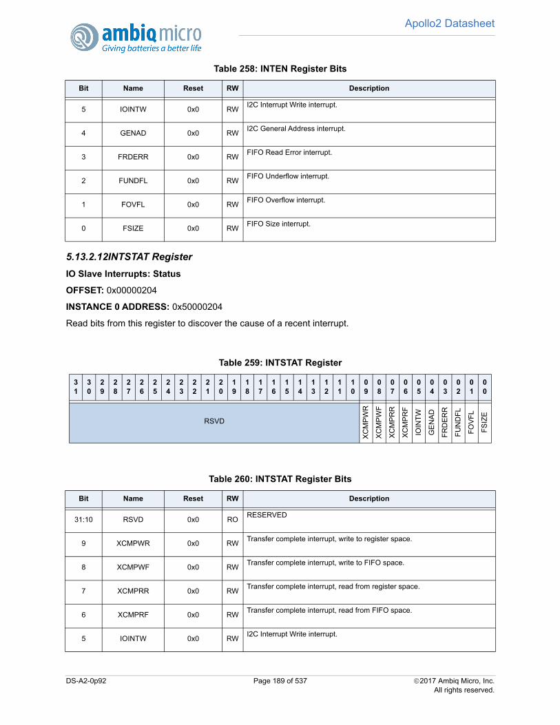
Apollo2 Datasheet
5.13.2.12INTSTAT Register
IO Slave Interrupts: Status
OFFSET: 0x00000204
INSTANCE 0 ADDRESS: 0x50000204
Read bits from this register to discover the cause of a recent interrupt.
5 IOINTW 0x0 RWI2C Interrupt Write interrupt.
4 GENAD 0x0 RWI2C General Address interrupt.
3 FRDERR 0x0 RWFIFO Read Error interrupt.
2 FUNDFL 0x0 RWFIFO Underflow interrupt.
1 FOVFL 0x0 RWFIFO Overflow interrupt.
0 FSIZE 0x0 RWFIFO Size interrupt.
Table 259: INTSTAT Register
31
30
29
28
27
26
25
24
23
22
21
20
19
18
17
16
15
14
13
12
11
10
09
08
07
06
05
04
03
02
01
00
RSVD
XC
MP
WR
XC
MP
WF
XC
MP
RR
XC
MP
RF
IOIN
TW
GE
NA
D
FR
DE
RR
FU
ND
FL
FO
VF
L
FS
IZE
Table 260: INTSTAT Register Bits
Bit Name Reset RW Description
31:10 RSVD 0x0 RORESERVED
9 XCMPWR 0x0 RWTransfer complete interrupt, write to register space.
8 XCMPWF 0x0 RWTransfer complete interrupt, write to FIFO space.
7 XCMPRR 0x0 RWTransfer complete interrupt, read from register space.
6 XCMPRF 0x0 RWTransfer complete interrupt, read from FIFO space.
5 IOINTW 0x0 RWI2C Interrupt Write interrupt.
Table 258: INTEN Register Bits
Bit Name Reset RW Description
DS-A2-0p92 Page 189 of 537 2017 Ambiq Micro, Inc.All rights reserved.
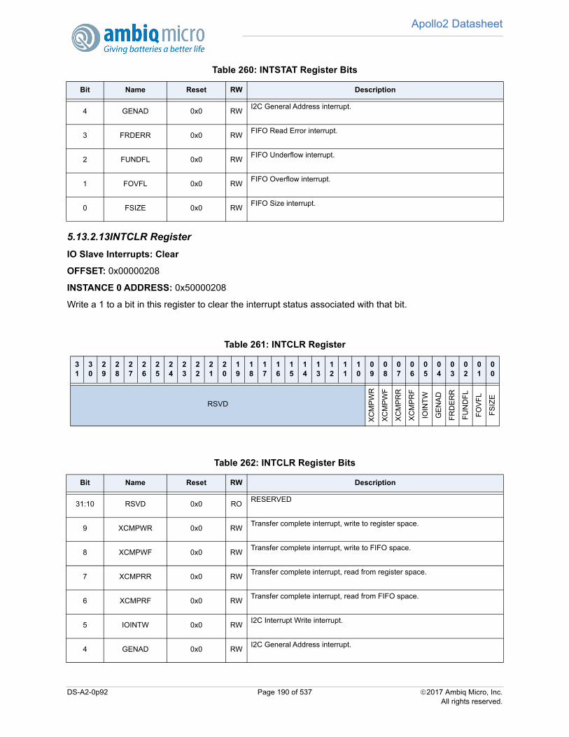
Apollo2 Datasheet
5.13.2.13INTCLR Register
IO Slave Interrupts: Clear
OFFSET: 0x00000208
INSTANCE 0 ADDRESS: 0x50000208
Write a 1 to a bit in this register to clear the interrupt status associated with that bit.
4 GENAD 0x0 RWI2C General Address interrupt.
3 FRDERR 0x0 RWFIFO Read Error interrupt.
2 FUNDFL 0x0 RWFIFO Underflow interrupt.
1 FOVFL 0x0 RWFIFO Overflow interrupt.
0 FSIZE 0x0 RWFIFO Size interrupt.
Table 261: INTCLR Register
31
30
29
28
27
26
25
24
23
22
21
20
19
18
17
16
15
14
13
12
11
10
09
08
07
06
05
04
03
02
01
00
RSVD
XC
MP
WR
XC
MP
WF
XC
MP
RR
XC
MP
RF
IOIN
TW
GE
NA
D
FR
DE
RR
FU
ND
FL
FO
VF
L
FS
IZE
Table 262: INTCLR Register Bits
Bit Name Reset RW Description
31:10 RSVD 0x0 RORESERVED
9 XCMPWR 0x0 RWTransfer complete interrupt, write to register space.
8 XCMPWF 0x0 RWTransfer complete interrupt, write to FIFO space.
7 XCMPRR 0x0 RWTransfer complete interrupt, read from register space.
6 XCMPRF 0x0 RWTransfer complete interrupt, read from FIFO space.
5 IOINTW 0x0 RWI2C Interrupt Write interrupt.
4 GENAD 0x0 RWI2C General Address interrupt.
Table 260: INTSTAT Register Bits
Bit Name Reset RW Description
DS-A2-0p92 Page 190 of 537 2017 Ambiq Micro, Inc.All rights reserved.
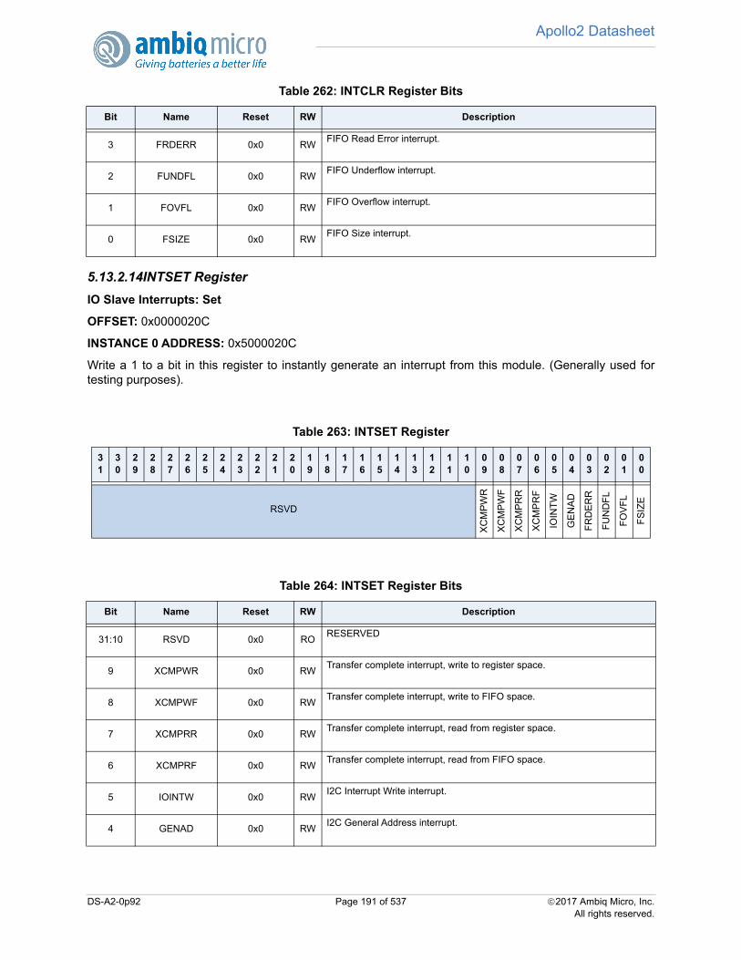
Apollo2 Datasheet
5.13.2.14INTSET Register
IO Slave Interrupts: Set
OFFSET: 0x0000020C
INSTANCE 0 ADDRESS: 0x5000020C
Write a 1 to a bit in this register to instantly generate an interrupt from this module. (Generally used fortesting purposes).
3 FRDERR 0x0 RWFIFO Read Error interrupt.
2 FUNDFL 0x0 RWFIFO Underflow interrupt.
1 FOVFL 0x0 RWFIFO Overflow interrupt.
0 FSIZE 0x0 RWFIFO Size interrupt.
Table 263: INTSET Register
31
30
29
28
27
26
25
24
23
22
21
20
19
18
17
16
15
14
13
12
11
10
09
08
07
06
05
04
03
02
01
00
RSVD
XC
MP
WR
XC
MP
WF
XC
MP
RR
XC
MP
RF
IOIN
TW
GE
NA
D
FR
DE
RR
FU
ND
FL
FO
VF
L
FS
IZE
Table 264: INTSET Register Bits
Bit Name Reset RW Description
31:10 RSVD 0x0 RORESERVED
9 XCMPWR 0x0 RWTransfer complete interrupt, write to register space.
8 XCMPWF 0x0 RWTransfer complete interrupt, write to FIFO space.
7 XCMPRR 0x0 RWTransfer complete interrupt, read from register space.
6 XCMPRF 0x0 RWTransfer complete interrupt, read from FIFO space.
5 IOINTW 0x0 RWI2C Interrupt Write interrupt.
4 GENAD 0x0 RWI2C General Address interrupt.
Table 262: INTCLR Register Bits
Bit Name Reset RW Description
DS-A2-0p92 Page 191 of 537 2017 Ambiq Micro, Inc.All rights reserved.
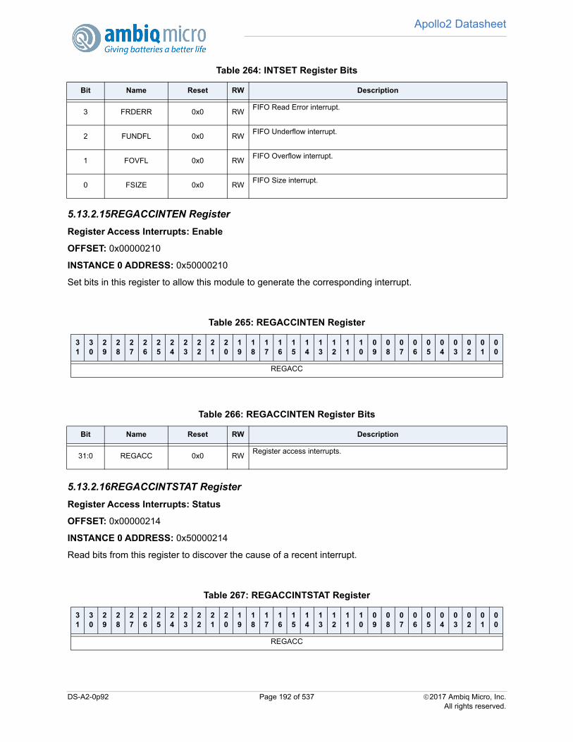
Apollo2 Datasheet
5.13.2.15REGACCINTEN Register
Register Access Interrupts: Enable
OFFSET: 0x00000210
INSTANCE 0 ADDRESS: 0x50000210
Set bits in this register to allow this module to generate the corresponding interrupt.
5.13.2.16REGACCINTSTAT Register
Register Access Interrupts: Status
OFFSET: 0x00000214
INSTANCE 0 ADDRESS: 0x50000214
Read bits from this register to discover the cause of a recent interrupt.
3 FRDERR 0x0 RWFIFO Read Error interrupt.
2 FUNDFL 0x0 RWFIFO Underflow interrupt.
1 FOVFL 0x0 RWFIFO Overflow interrupt.
0 FSIZE 0x0 RWFIFO Size interrupt.
Table 265: REGACCINTEN Register
31
30
29
28
27
26
25
24
23
22
21
20
19
18
17
16
15
14
13
12
11
10
09
08
07
06
05
04
03
02
01
00
REGACC
Table 266: REGACCINTEN Register Bits
Bit Name Reset RW Description
31:0 REGACC 0x0 RWRegister access interrupts.
Table 267: REGACCINTSTAT Register
31
30
29
28
27
26
25
24
23
22
21
20
19
18
17
16
15
14
13
12
11
10
09
08
07
06
05
04
03
02
01
00
REGACC
Table 264: INTSET Register Bits
Bit Name Reset RW Description
DS-A2-0p92 Page 192 of 537 2017 Ambiq Micro, Inc.All rights reserved.
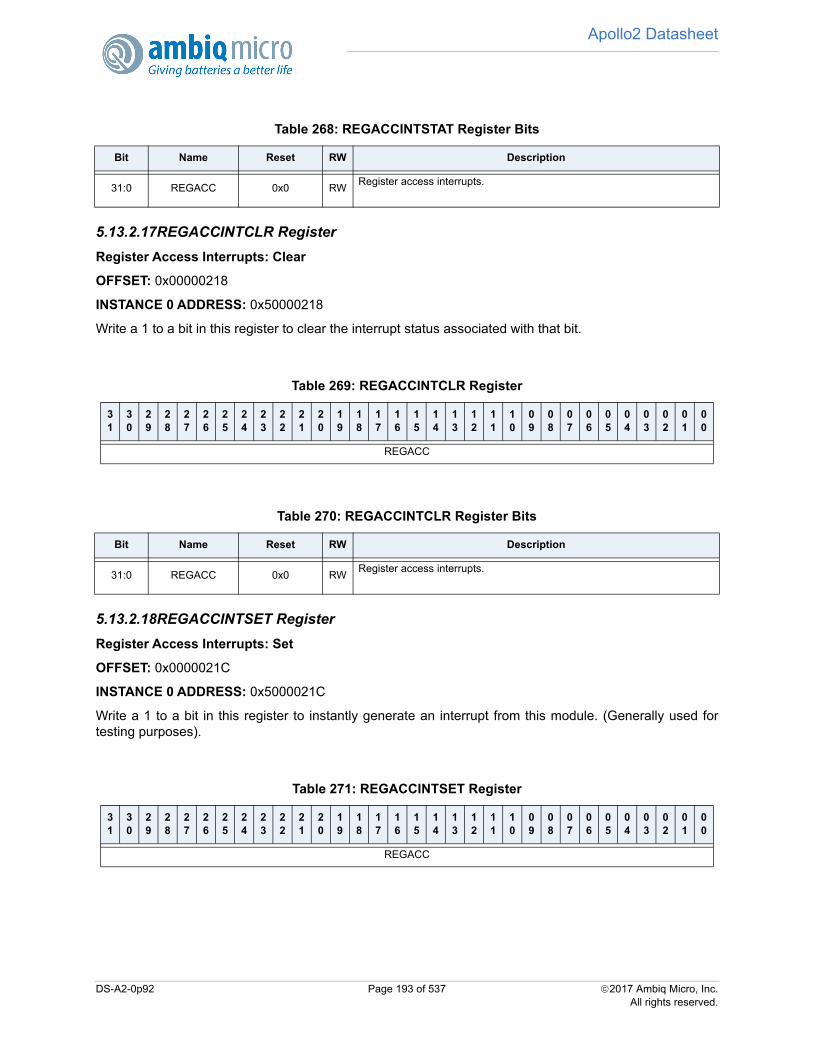
Apollo2 Datasheet
5.13.2.17REGACCINTCLR Register
Register Access Interrupts: Clear
OFFSET: 0x00000218
INSTANCE 0 ADDRESS: 0x50000218
Write a 1 to a bit in this register to clear the interrupt status associated with that bit.
5.13.2.18REGACCINTSET Register
Register Access Interrupts: Set
OFFSET: 0x0000021C
INSTANCE 0 ADDRESS: 0x5000021C
Write a 1 to a bit in this register to instantly generate an interrupt from this module. (Generally used fortesting purposes).
Table 268: REGACCINTSTAT Register Bits
Bit Name Reset RW Description
31:0 REGACC 0x0 RWRegister access interrupts.
Table 269: REGACCINTCLR Register
31
30
29
28
27
26
25
24
23
22
21
20
19
18
17
16
15
14
13
12
11
10
09
08
07
06
05
04
03
02
01
00
REGACC
Table 270: REGACCINTCLR Register Bits
Bit Name Reset RW Description
31:0 REGACC 0x0 RWRegister access interrupts.
Table 271: REGACCINTSET Register
31
30
29
28
27
26
25
24
23
22
21
20
19
18
17
16
15
14
13
12
11
10
09
08
07
06
05
04
03
02
01
00
REGACC
DS-A2-0p92 Page 193 of 537 2017 Ambiq Micro, Inc.All rights reserved.
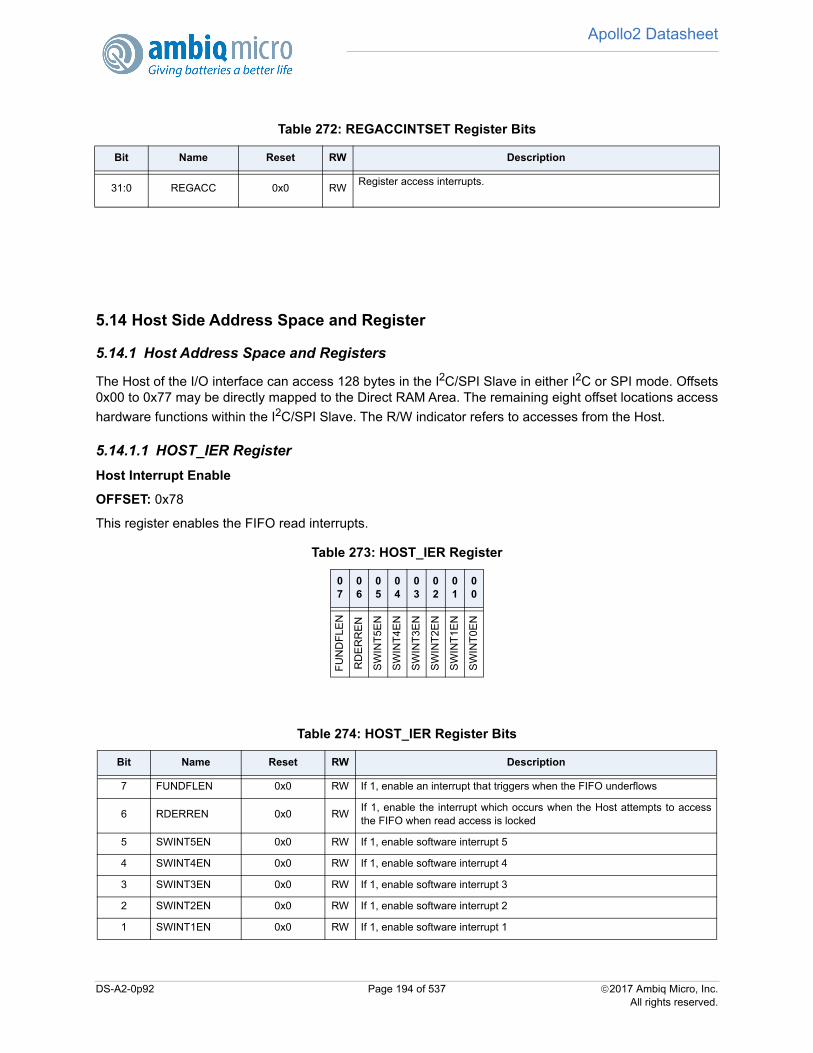
Apollo2 Datasheet
5.14 Host Side Address Space and Register
5.14.1 Host Address Space and Registers
The Host of the I/O interface can access 128 bytes in the I2C/SPI Slave in either I2C or SPI mode. Offsets0x00 to 0x77 may be directly mapped to the Direct RAM Area. The remaining eight offset locations access
hardware functions within the I2C/SPI Slave. The R/W indicator refers to accesses from the Host.
5.14.1.1 HOST_IER Register
Host Interrupt Enable
OFFSET: 0x78
This register enables the FIFO read interrupts.
Table 272: REGACCINTSET Register Bits
Bit Name Reset RW Description
31:0 REGACC 0x0 RWRegister access interrupts.
Table 273: HOST_IER Register
07
06
05
04
03
02
01
00
FU
ND
FLE
N
RD
ER
RE
N
SW
INT
5EN
SW
INT
4EN
SW
INT
3EN
SW
INT
2EN
SW
INT
1EN
SW
INT
0EN
Table 274: HOST_IER Register Bits
Bit Name Reset RW Description
7 FUNDFLEN 0x0 RW If 1, enable an interrupt that triggers when the FIFO underflows
6 RDERREN 0x0 RWIf 1, enable the interrupt which occurs when the Host attempts to accessthe FIFO when read access is locked
5 SWINT5EN 0x0 RW If 1, enable software interrupt 5
4 SWINT4EN 0x0 RW If 1, enable software interrupt 4
3 SWINT3EN 0x0 RW If 1, enable software interrupt 3
2 SWINT2EN 0x0 RW If 1, enable software interrupt 2
1 SWINT1EN 0x0 RW If 1, enable software interrupt 1
DS-A2-0p92 Page 194 of 537 2017 Ambiq Micro, Inc.All rights reserved.
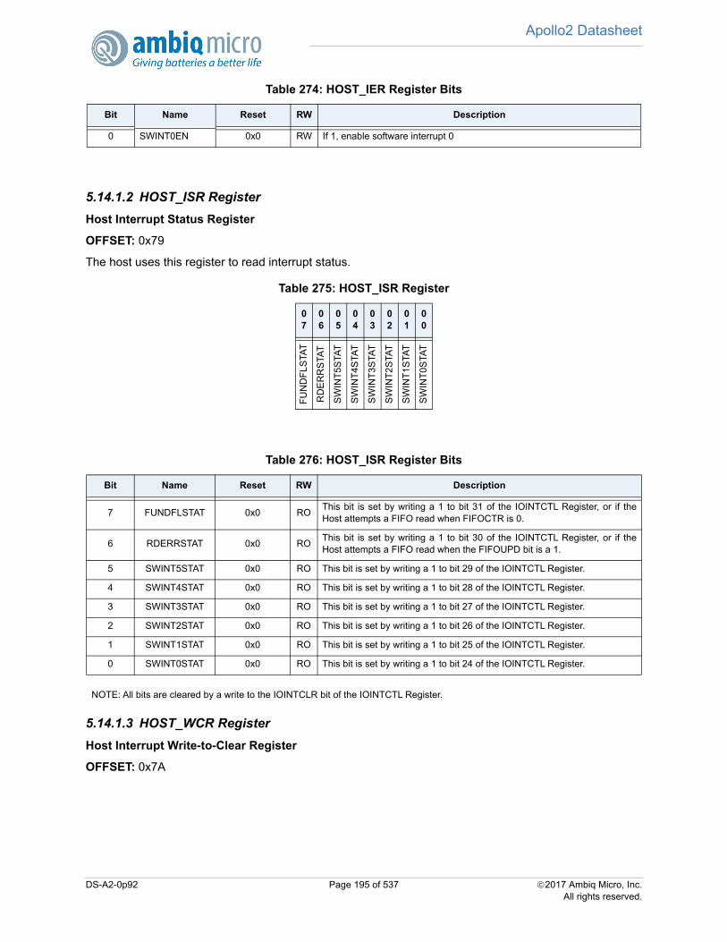
Apollo2 Datasheet
5.14.1.2 HOST_ISR Register
Host Interrupt Status Register
OFFSET: 0x79
The host uses this register to read interrupt status.
NOTE: All bits are cleared by a write to the IOINTCLR bit of the IOINTCTL Register.
5.14.1.3 HOST_WCR Register
Host Interrupt Write-to-Clear Register
OFFSET: 0x7A
0 SWINT0EN 0x0 RW If 1, enable software interrupt 0
Table 275: HOST_ISR Register
07
06
05
04
03
02
01
00
FU
ND
FLS
TAT
RD
ER
RS
TAT
SW
INT
5STA
T
SW
INT
4STA
T
SW
INT
3STA
T
SW
INT
2STA
T
SW
INT
1STA
T
SW
INT
0STA
T
Table 276: HOST_ISR Register Bits
Bit Name Reset RW Description
7 FUNDFLSTAT 0x0 ROThis bit is set by writing a 1 to bit 31 of the IOINTCTL Register, or if theHost attempts a FIFO read when FIFOCTR is 0.
6 RDERRSTAT 0x0 ROThis bit is set by writing a 1 to bit 30 of the IOINTCTL Register, or if theHost attempts a FIFO read when the FIFOUPD bit is a 1.
5 SWINT5STAT 0x0 RO This bit is set by writing a 1 to bit 29 of the IOINTCTL Register.
4 SWINT4STAT 0x0 RO This bit is set by writing a 1 to bit 28 of the IOINTCTL Register.
3 SWINT3STAT 0x0 RO This bit is set by writing a 1 to bit 27 of the IOINTCTL Register.
2 SWINT2STAT 0x0 RO This bit is set by writing a 1 to bit 26 of the IOINTCTL Register.
1 SWINT1STAT 0x0 RO This bit is set by writing a 1 to bit 25 of the IOINTCTL Register.
0 SWINT0STAT 0x0 RO This bit is set by writing a 1 to bit 24 of the IOINTCTL Register.
Table 274: HOST_IER Register Bits
Bit Name Reset RW Description
DS-A2-0p92 Page 195 of 537 2017 Ambiq Micro, Inc.All rights reserved.
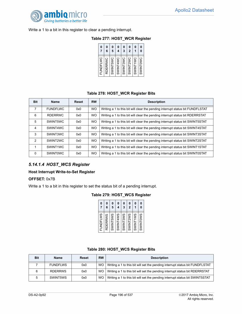
Apollo2 Datasheet
Write a 1 to a bit in this register to clear a pending interrupt.
5.14.1.4 HOST_WCS Register
Host Interrupt Write-to-Set Register
OFFSET: 0x7B
Write a 1 to a bit in this register to set the status bit of a pending interrupt.
Table 277: HOST_WCR Register
07
06
05
04
03
02
01
00
FU
ND
FLW
C
RD
ER
RW
C
SW
INT
5W
C
SW
INT
4W
C
SW
INT
3W
C
SW
INT
2W
C
SW
INT
1W
C
SW
INT
0W
C
Table 278: HOST_WCR Register Bits
Bit Name Reset RW Description
7 FUNDFLWC 0x0 WO Writing a 1 to this bit will clear the pending interrupt status bit FUNDFLSTAT
6 RDERRWC 0x0 WO Writing a 1 to this bit will clear the pending interrupt status bit RDERRSTAT
5 SWINT5WC 0x0 WO Writing a 1 to this bit will clear the pending interrupt status bit SWINT5STAT
4 SWINT4WC 0x0 WO Writing a 1 to this bit will clear the pending interrupt status bit SWINT4STAT
3 SWINT3WC 0x0 WO Writing a 1 to this bit will clear the pending interrupt status bit SWINT3STAT
2 SWINT2WC 0x0 WO Writing a 1 to this bit will clear the pending interrupt status bit SWINT2STAT
1 SWINT1WC 0x0 WO Writing a 1 to this bit will clear the pending interrupt status bit SWINT1STAT
0 SWINT0WC 0x0 WO Writing a 1 to this bit will clear the pending interrupt status bit SWINT0STAT
Table 279: HOST_WCS Register
07
06
05
04
03
02
01
00
FU
ND
FLW
S
RD
ER
RW
S
SW
INT
5WS
SW
INT
4WS
SW
INT
3WS
SW
INT
2WS
SW
INT
1WS
SW
INT
0WS
Table 280: HOST_WCS Register Bits
Bit Name Reset RW Description
7 FUNDFLWS 0x0 WO Writing a 1 to this bit will set the pending interrupt status bit FUNDFLSTAT
6 RDERRWS 0x0 WO Writing a 1 to this bit will set the pending interrupt status bit RDERRSTAT
5 SWINT5WS 0x0 WO Writing a 1 to this bit will set the pending interrupt status bit SWINT5STAT
DS-A2-0p92 Page 196 of 537 2017 Ambiq Micro, Inc.All rights reserved.
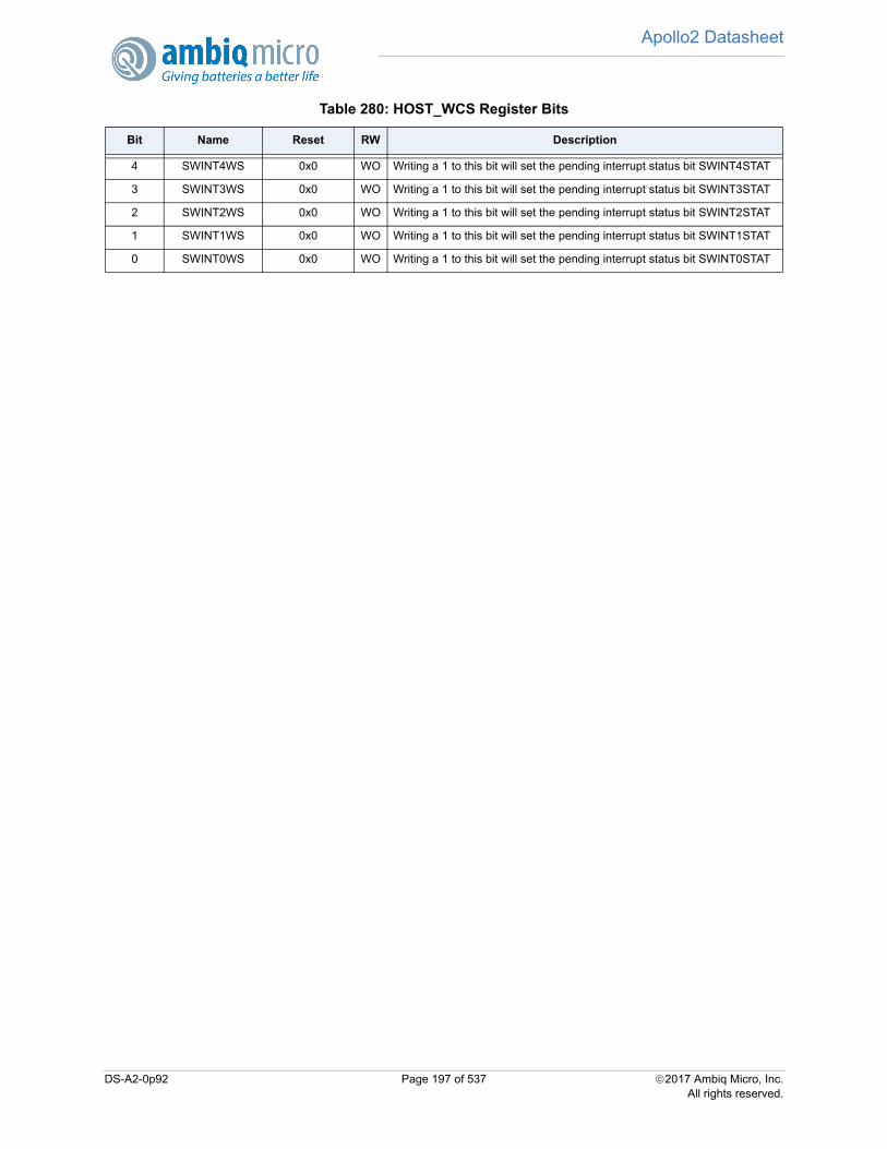
Apollo2 Datasheet
4 SWINT4WS 0x0 WO Writing a 1 to this bit will set the pending interrupt status bit SWINT4STAT
3 SWINT3WS 0x0 WO Writing a 1 to this bit will set the pending interrupt status bit SWINT3STAT
2 SWINT2WS 0x0 WO Writing a 1 to this bit will set the pending interrupt status bit SWINT2STAT
1 SWINT1WS 0x0 WO Writing a 1 to this bit will set the pending interrupt status bit SWINT1STAT
0 SWINT0WS 0x0 WO Writing a 1 to this bit will set the pending interrupt status bit SWINT0STAT
Table 280: HOST_WCS Register Bits
Bit Name Reset RW Description
DS-A2-0p92 Page 197 of 537 2017 Ambiq Micro, Inc.All rights reserved.
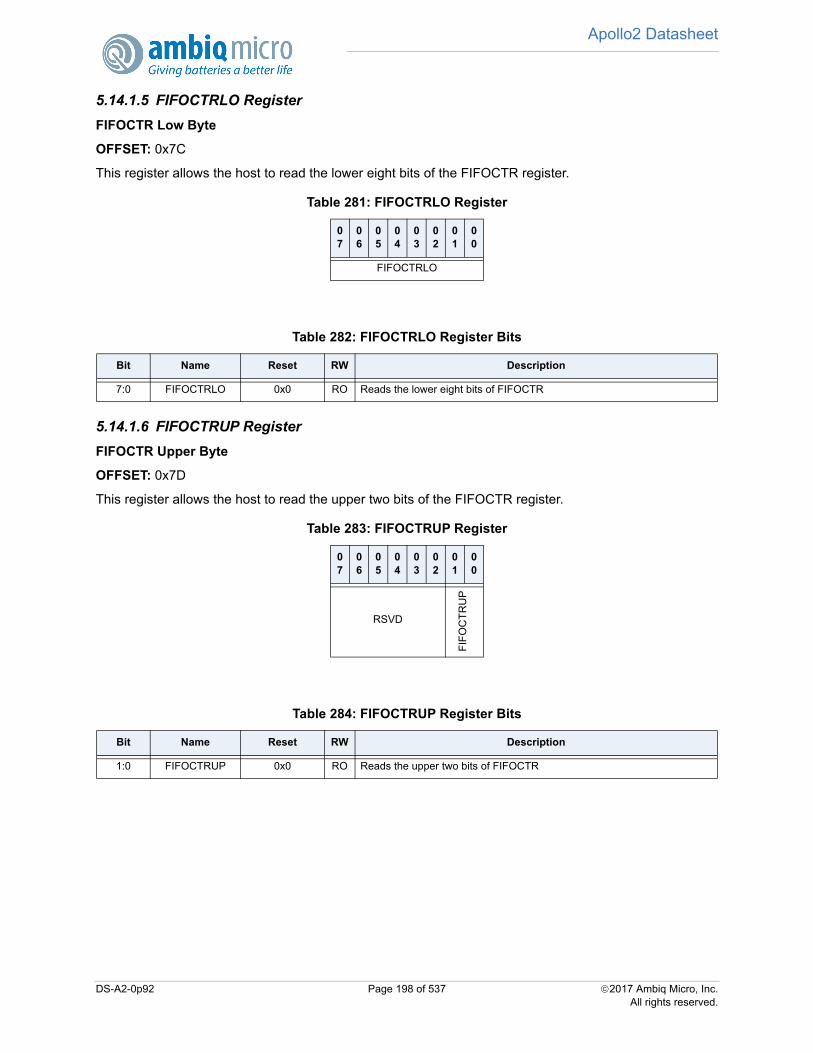
Apollo2 Datasheet
5.14.1.5 FIFOCTRLO Register
FIFOCTR Low Byte
OFFSET: 0x7C
This register allows the host to read the lower eight bits of the FIFOCTR register.
5.14.1.6 FIFOCTRUP Register
FIFOCTR Upper Byte
OFFSET: 0x7D
This register allows the host to read the upper two bits of the FIFOCTR register.
Table 281: FIFOCTRLO Register
07
06
05
04
03
02
01
00
FIFOCTRLO
Table 282: FIFOCTRLO Register Bits
Bit Name Reset RW Description
7:0 FIFOCTRLO 0x0 RO Reads the lower eight bits of FIFOCTR
Table 283: FIFOCTRUP Register
07
06
05
04
03
02
01
00
RSVD
FIF
OC
TR
UP
Table 284: FIFOCTRUP Register Bits
Bit Name Reset RW Description
1:0 FIFOCTRUP 0x0 RO Reads the upper two bits of FIFOCTR
DS-A2-0p92 Page 198 of 537 2017 Ambiq Micro, Inc.All rights reserved.
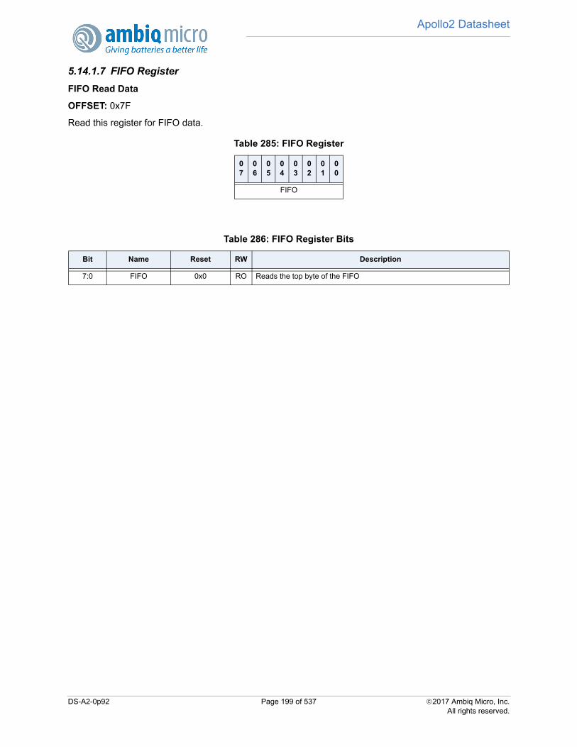
Apollo2 Datasheet
5.14.1.7 FIFO Register
FIFO Read Data
OFFSET: 0x7F
Read this register for FIFO data.
Table 285: FIFO Register
07
06
05
04
03
02
01
00
FIFO
Table 286: FIFO Register Bits
Bit Name Reset RW Description
7:0 FIFO 0x0 RO Reads the top byte of the FIFO
DS-A2-0p92 Page 199 of 537 2017 Ambiq Micro, Inc.All rights reserved.
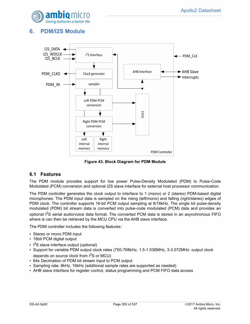
Apollo2 Datasheet
6. PDM/I2S Module
Figure 43. Block Diagram for PDM Module
6.1 FeaturesThe PDM module provides support for low power Pulse-Density Modulated (PDM) to Pulse-CodeModulated (PCM) conversion and optional I2S slave interface for external host processor communication.
The PDM controller generates the clock output to interface to 1 (mono) or 2 (stereo) PDM-based digitalmicrophones. The PDM input data is sampled on the rising (left/mono) and falling (right/stereo) edges ofPDM clock. The controller supports 16-bit PCM output sampling at 8/16kHz. The single bit pulse-densitymodulated (PDM) bit stream data is converted into pulse-code modulated (PCM) data and provides an
optional I2S serial audio/voice data format. The converted PCM data is stored in an asynchronous FIFOwhere is can then be retrieved by the MCU CPU via the AHB slave interface.
The PDM controller includes the following features:
Stereo or mono PDM input 16bit PCM digital output
I2S slave interface output (optional) Support for variable PDM output clock rates (750-768kHz, 1.5-1.536MHz, 3-3.072MHz: output clock
depends on source clock from I2S or MCU) 64x Decimation of PDM bit stream input to PCM output Sampling rate: 8kHz, 16kHz (additional sample rates are supported as needed) AHB slave interface for register control, status programming and PCM FIFO data access
PDM Controller
sampler
FIFO
Left internal memory
Right internal memory
Right PDM-PCM conversion
PDM_IN
Left PDM-PCM conversion
AHB Interface
I2S Interface
Clock generatorPDM_CLKO
I2S_WDCLKI2S_BCLK
I2S_DATA
AHB SlaveInterrupts
PDM_CLK
DS-A2-0p92 Page 200 of 537 2017 Ambiq Micro, Inc.All rights reserved.
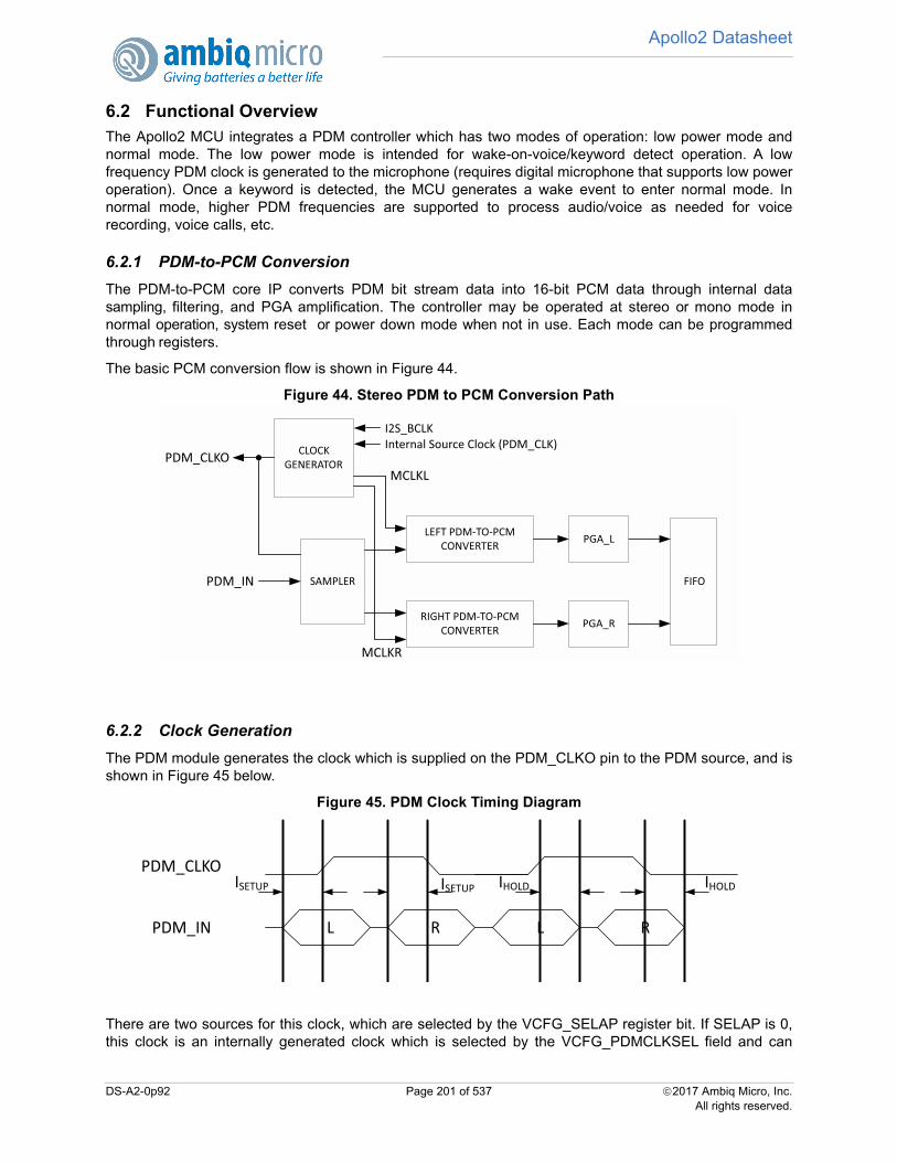
Apollo2 Datasheet
6.2 Functional OverviewThe Apollo2 MCU integrates a PDM controller which has two modes of operation: low power mode andnormal mode. The low power mode is intended for wake-on-voice/keyword detect operation. A lowfrequency PDM clock is generated to the microphone (requires digital microphone that supports low poweroperation). Once a keyword is detected, the MCU generates a wake event to enter normal mode. Innormal mode, higher PDM frequencies are supported to process audio/voice as needed for voicerecording, voice calls, etc.
6.2.1 PDM-to-PCM Conversion
The PDM-to-PCM core IP converts PDM bit stream data into 16-bit PCM data through internal datasampling, filtering, and PGA amplification. The controller may be operated at stereo or mono mode innormal operation, system reset or power down mode when not in use. Each mode can be programmedthrough registers.
The basic PCM conversion flow is shown in Figure 44.
Figure 44. Stereo PDM to PCM Conversion Path
6.2.2 Clock Generation
The PDM module generates the clock which is supplied on the PDM_CLKO pin to the PDM source, and isshown in Figure 45 below.
Figure 45. PDM Clock Timing Diagram
There are two sources for this clock, which are selected by the VCFG_SELAP register bit. If SELAP is 0,this clock is an internally generated clock which is selected by the VCFG_PDMCLKSEL field and can
SAMPLER FIFO
PGA_RRIGHT PDM-TO-PCM CONVERTER
LEFT PDM-TO-PCM CONVERTER
CLOCK GENERATORPDM_CLKO
I2S_BCLK
PGA_L
Internal Source Clock (PDM_CLK)
MCLKR
MCLKL
PDM_IN
L R L R
ISETUP ISETUP IHOLD IHOLD
PDM_CLKO
PDM_IN
DS-A2-0p92 Page 201 of 537 2017 Ambiq Micro, Inc.All rights reserved.

Apollo2 Datasheet
range from 12 MHz to 187.5 KHz, and is enabled by setting the PCFG_PDMCLK bit. These clockselections are derived from the internal 48 MHz HFRC oscillator and therefore will have some frequencyvariation. If SELAP is 1, this clock is supplied externally on the I2S_BCLK pin. The input clock is used asthe clock of the internal PDM logic, and therefore the lowest acceptable frequency should be selected tominimize power. The PDM logic includes separately clocked sections for each of the left and rightchannels.
The input clock is divided by 1, 2, 3 or 4 as selected by the PCFG_MCLKDIV field to produce thePDM_CLKO output.
NOTE: If achieving a nominal 50% duty cycle PDM output clock is important, then using a clock divider ofdivide-by-3 (MCKDIV3) for PCFG_MCLKDIV should be avoided as the resulting divided clock has a dutycycle of 67%, not the expected 50%. The other PCFG_MCLKDIV settings, MCKDIV1, MCKDIV2 andMCKDIV4 can be used to generate an output clock close to 50% duty cycle. See Table 287 for reference.
The following equations are for reference showing the relationship between SINC_RATE, MCLKDIV,sample rate and OSR.
FPDM_CLK = FS X 2 X SINC_RATE X MCLKDIV
FPDM_CLKO = FS X 2 X SINC_RATE
OSR = FPDM_CLKO / FS = 2 X SINC_RATE
The PDM module also requires a system clock to operate, which is enabled by the VCFG_IOCLKENregister bit. This bit should be kept at 0 whenever the PDM is not capturing input data to minimize powerconsumption.
The serial PDM input data is oversampled by a value specified in the PCFG_SINCRATE register field toproduce the PCM data. The resulting PCM data rate is the PDM_CLKO frequency divided by theSINCRATE value and divided by 2. The table below shows some examples of frequency selection.
The PDM controller also includes separate clock gates for left and right channel. This allows for lowerpower operation in mono microphone configuration.
6.2.3 Clock Switching
The Apollo2 MCU supports dual-mode clock sourcing for PDM microphone operation. The first mode isclock sourcing from the MCU directly (via divided down HFRC reference). The second mode is clocksourcing from an external host via the I2S_BCLK.
Table 287: PDM Clock Output Reference Table
FS (kHz) Duty Cycle (%)
FPDM_CLKO(kHz) OSR MCLKDIVSYNC_RATE
Clock Source
7.8125 50 750 96 MCKDIV1 48 750kHz (MCU HFRC)
15.625 50 750 48 MCKDIV1 24 750kHz (MCU HFRC)
15.625 50 1500 96 MCKDIV1 48 1.5MHz (MCU HFRC)
7.8125 67 1000 128 MCKDIV3 64 3MHz (MCU HFRC)
8 50 768 96 MCKDIV1 48 768kHz (external I2S_BCLK)
16 50 768 48 MCKDIV1 24 768kHz (external I2S_BCLK)
16 50 3072 192 MCKDIV4 96 12.288MHz (external I2S BCLK)
DS-A2-0p92 Page 202 of 537 2017 Ambiq Micro, Inc.All rights reserved.
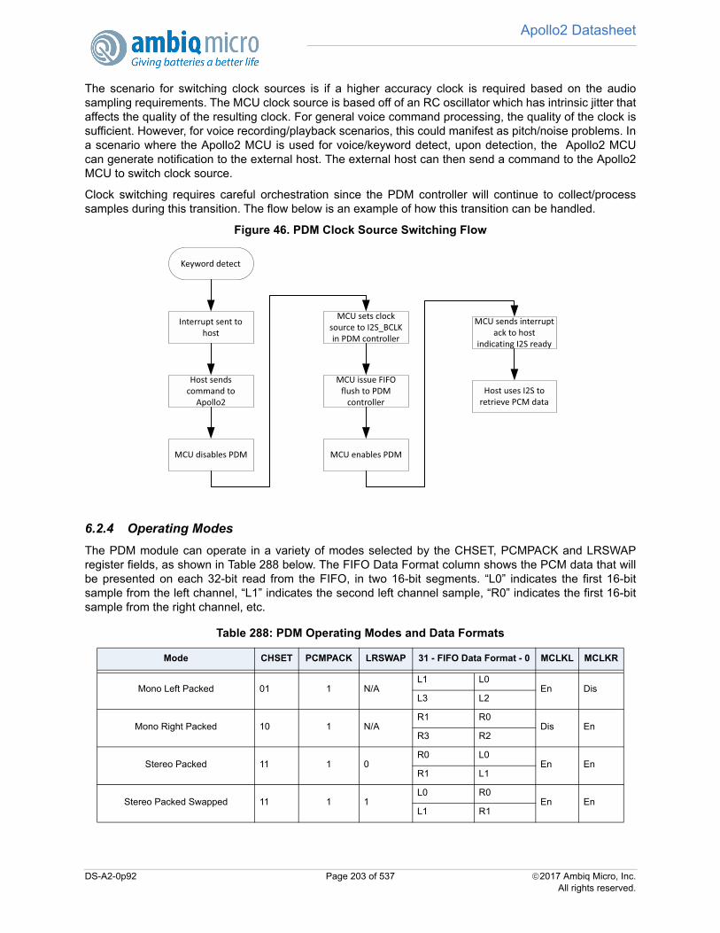
Apollo2 Datasheet
The scenario for switching clock sources is if a higher accuracy clock is required based on the audiosampling requirements. The MCU clock source is based off of an RC oscillator which has intrinsic jitter thataffects the quality of the resulting clock. For general voice command processing, the quality of the clock issufficient. However, for voice recording/playback scenarios, this could manifest as pitch/noise problems. Ina scenario where the Apollo2 MCU is used for voice/keyword detect, upon detection, the Apollo2 MCUcan generate notification to the external host. The external host can then send a command to the Apollo2MCU to switch clock source.
Clock switching requires careful orchestration since the PDM controller will continue to collect/processsamples during this transition. The flow below is an example of how this transition can be handled.
Figure 46. PDM Clock Source Switching Flow
6.2.4 Operating Modes
The PDM module can operate in a variety of modes selected by the CHSET, PCMPACK and LRSWAPregister fields, as shown in Table 288 below. The FIFO Data Format column shows the PCM data that willbe presented on each 32-bit read from the FIFO, in two 16-bit segments. “L0” indicates the first 16-bitsample from the left channel, “L1” indicates the second left channel sample, “R0” indicates the first 16-bitsample from the right channel, etc.
Table 288: PDM Operating Modes and Data Formats
Mode CHSET PCMPACK LRSWAP 31 - FIFO Data Format - 0 MCLKL MCLKR
Mono Left Packed 01 1 N/AL1 L0
En DisL3 L2
Mono Right Packed 10 1 N/AR1 R0
Dis EnR3 R2
Stereo Packed 11 1 0R0 L0
En EnR1 L1
Stereo Packed Swapped 11 1 1L0 R0
En EnL1 R1
Keyword detect
Interrupt sent to host
Host sends command to
Apollo2
MCU disables PDM
MCU sets clock source to I2S_BCLK in PDM controller
MCU issue FIFO flush to PDM
controller
MCU enables PDM
MCU sends interrupt ack to host
indicating I2S ready
Host uses I2S to retrieve PCM data
DS-A2-0p92 Page 203 of 537 2017 Ambiq Micro, Inc.All rights reserved.

Apollo2 Datasheet
The MCLKL and MCLKR columns indicate whether the left and right channel clocks are enabled ordisabled.
6.2.5 FIFO Control and Interrupts
The PCM data is retrieved from the PDM module through a 256-word FIFO, read at the FRD Register. Thenumber of words currently in the FIFO (0 to 256) is read in the FR_FIFOCNT field. If the FLUSH Registeris written (with any value) FIFOCNT is set to 0 and any data in the FIFO is discarded. Each read from theFRD Register will decrement the FIFOCNT value, and FIFOCNT will be incremented each time new PCMdata is written into the FIFO.
There are three interrupts which are generated based on the number of words in the FIFO. The UNDFLinterrupt is generated if software reads from the FRD register when FIFOCNT is 0. The OVF interrupt isgenerated if PCM data is received when FIFOCNT is 256. The THR interrupt is set if PCM data is receivedand FIFOCNT is greater than or equal to the value in the FTHR_FIFOTHR Register field.
6.2.6 Digital Volume Gain
The PDM controller supports digital volume control with a range from -12dB to +10.5 dB in steps of 1.5 dB.It is programmed by register PGA_L and PGA_R for both left and right channels.
Mono Left Unpacked 01 0 N/A0000 L0
En Dis0000 L1
Mono Right Unpacked 10 0 N/A0000 R0
Dis En0000 R1
Stereo Unpacked 11 0 00000 L0
En En0000 R0
Stereo Unpacked Swapped 11 0 10000 R0
En En0000 L0
Disabled 00 N/A N/A0000 0000
Dis Dis0000 0000
Table 289: Digital Volume Control
Port Name Default Description
PGA_L[3:0] 0000
Left Channel PGA Gain: +1.5dB/step
7 +10.5dB; 6 +9.0dB;5 +7.5dB; 4 +6.0dB;
3 +4.5dB; 2 +3.0dB;
1 +1.5dB; 0 0.0dB;
15 -1.5dB; 14 -3.0dB;
13 -4.5dB; 12 -6.0dB;
11 -7.5dB; 10 -9.0dB;
9 -10.5dB; 8 -12dB
Table 288: PDM Operating Modes and Data Formats
Mode CHSET PCMPACK LRSWAP 31 - FIFO Data Format - 0 MCLKL MCLKR
DS-A2-0p92 Page 204 of 537 2017 Ambiq Micro, Inc.All rights reserved.
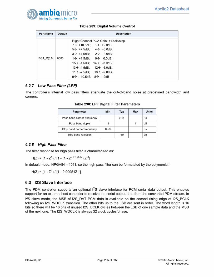
Apollo2 Datasheet
6.2.7 Low Pass Filter (LPF)
The controller’s internal low pass filters attenuate the out-of-band noise at predefined bandwidth andcorners.
6.2.8 High Pass Filter
The filter response for high pass filter is characterized as:
H(Z) = (1 - Z1) / [1 - (1 - 2-HPGAIN) Z-1]
In default mode, HPGAIN = 1011, so the high pass filter can be formulated by the polynomial:
H(Z) = (1 - Z1) / [1 - 0.99951Z-1]
6.3 I2S Slave Interface
The PDM controller supports an optional I2S slave interface for PCM serial data output. This enablessupport for an external host controller to receive the serial output data from the converted PDM stream. In
I2S slave mode, the MSB of I2S_DAT PCM data is available on the second rising edge of I2S_BCLKfollowing an I2S_WDCLK transition. The other bits up to the LSB are sent in order. The word length is 16bits so there will be 16 bits of unused I2S_BCLK cycles between the LSB of one sample data and the MSBof the next one. The I2S_WDCLK is always 32 clock cycles/phase.
PGA_R[3:0] 0000
Right Channel PGA Gain: +1.5dB/step 7 +10.5dB; 6 +9.0dB;5 +7.5dB; 4 +6.0dB;
3 +4.5dB; 2 +3.0dB;
1 +1.5dB; 0 0.0dB;
15 -1.5dB; 14 -3.0dB;
13 -4.5dB; 12 -6.0dB;
11 -7.5dB; 10 -9.0dB;
9 -10.5dB; 8 -12dB
Table 290: LPF Digital Filter Parameters
Parameter Min Typ Max Units
Pass band corner frequency 0.41 Fs
Pass band ripple -1 1 dB
Stop band corner frequency 0.59 Fs
Stop band rejection -60 dB
Table 289: Digital Volume Control
Port Name Default Description
DS-A2-0p92 Page 205 of 537 2017 Ambiq Micro, Inc.All rights reserved.
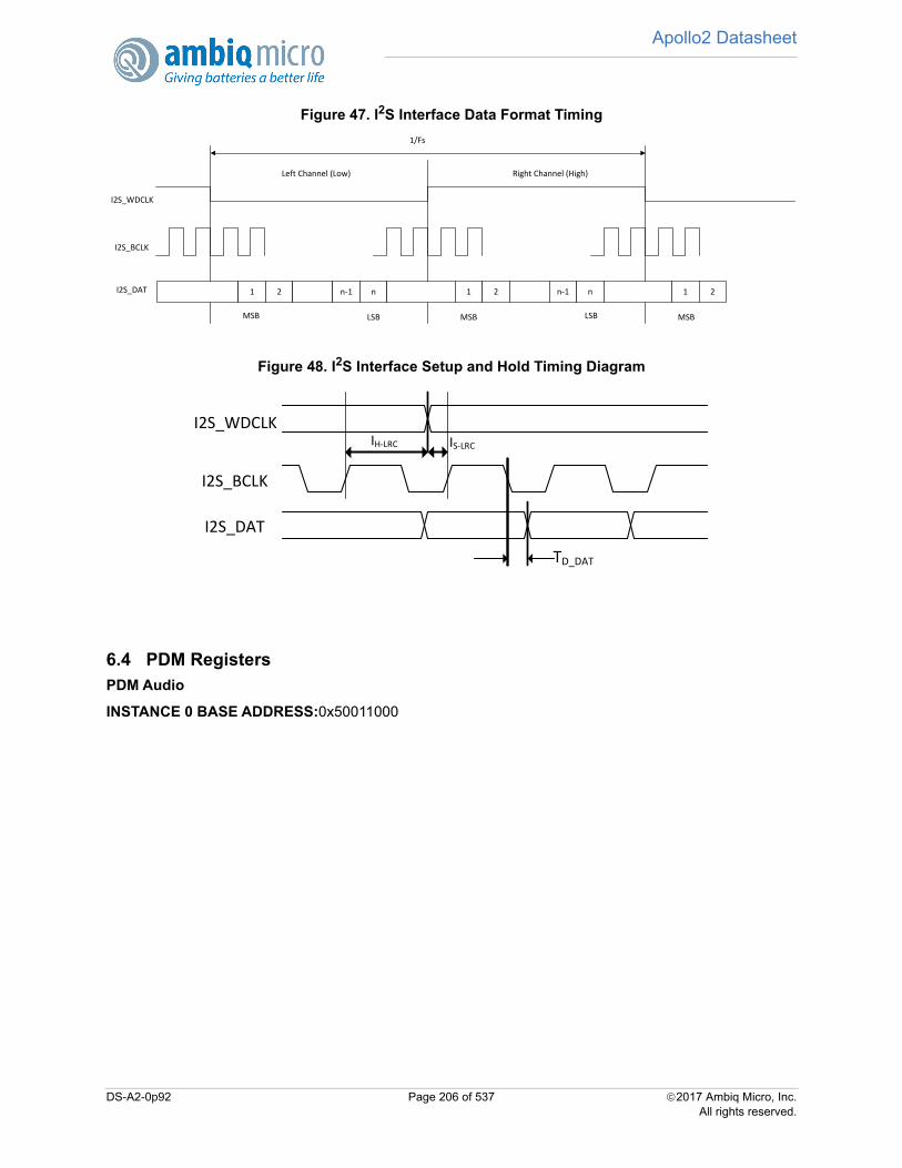
Apollo2 Datasheet
Figure 47. I2S Interface Data Format Timing
Figure 48. I2S Interface Setup and Hold Timing Diagram
6.4 PDM RegistersPDM Audio
INSTANCE 0 BASE ADDRESS:0x50011000
I2S_WDCLK
I2S_BCLK
I2S_DAT
Left Channel (Low) Right Channel (High)
1 2 n‐1 n 1 2 n‐1 n 1 2
MSB MSB MSBLSB LSB
1/Fs
IH‐LRC IS‐LRC
TD_DAT
I2S_WDCLK
I2S_BCLK
I2S_DAT
DS-A2-0p92 Page 206 of 537 2017 Ambiq Micro, Inc.All rights reserved.

Apollo2 Datasheet
6.4.1 Register Memory Map
Table 291: PDM Register Map
Address(s) Register Name Description
0x50011000 PCFG PDM Configuration Register
0x50011004 VCFG Voice Configuration Register
0x50011008 FR Voice Status Register
0x5001100C FRD FIFO Read
0x50011010 FLUSH FIFO Flush
0x50011014 FTHR FIFO Threshold
0x50011200 INTEN IO Master Interrupts: Enable
0x50011204 INTSTAT IO Master Interrupts: Status
0x50011208 INTCLR IO Master Interrupts: Clear
0x5001120C INTSET IO Master Interrupts: Set
DS-A2-0p92 Page 207 of 537 2017 Ambiq Micro, Inc.All rights reserved.
Apollo2 Datasheet
6.4.2 PDM Registers
6.4.2.1 PCFG Register
PDM Configuration Register
OFFSET: 0x00000000
INSTANCE 0 ADDRESS: 0x50011000
PDM Configuration Register
Table 292: PCFG Register
31
30
29
28
27
26
25
24
23
22
21
20
19
18
17
16
15
14
13
12
11
10
09
08
07
06
05
04
03
02
01
00
LR
SW
AP
PG
AR
IGH
T
PGALEFT RSVDM
CL
KD
IVSINCRATE
AD
CH
PD
HP
CU
TO
FF
CY
CLE
S
SO
FT
MU
TE
PD
MC
OR
E
Table 293: PCFG Register Bits
Bit Name Reset RW Description
31 LRSWAP 0x0 RW
Left/right channel swap.
EN = 0x1 - Swap left and right channels (FIFO Read RIGHT_LEFT).NOSWAP = 0x0 - No channel swapping (IFO Read LEFT_RIGHT).
30:27 PGARIGHT 0x0 RW
Right channel PGA gain.
M15DB = 0xF - -1.5 db gain.M300DB = 0xE - -3.0 db gain.M45DB = 0xD - -4.5 db gain.M60DB = 0xC - -6.0 db gain.M75DB = 0xB - -7.5 db gain.M90DB = 0xA - -9.0 db gain.M105DB = 0x9 - -10.5 db gain.M120DB = 0x8 - -12.0 db gain.P105DB = 0x7 - 10.5 db gain.P90DB = 0x6 - 9.0 db gain.P75DB = 0x5 - 7.5 db gain.P60DB = 0x4 - 6.0 db gain.P45DB = 0x3 - 4.5 db gain.P30DB = 0x2 - 3.0 db gain.P15DB = 0x1 - 1.5 db gain.0DB = 0x0 - 0.0 db gain.
DS-A2-0p92 Page 208 of 537 2017 Ambiq Micro, Inc.All rights reserved.

Apollo2 Datasheet
6.4.2.2 VCFG Register
Voice Configuration Register
OFFSET: 0x00000004
INSTANCE 0 ADDRESS: 0x50011004
Voice Configuration Register
26:23 PGALEFT 0x0 RW
Left channel PGA gain.
M15DB = 0xF - -1.5 db gain.M300DB = 0xE - -3.0 db gain.M45DB = 0xD - -4.5 db gain.M60DB = 0xC - -6.0 db gain.M75DB = 0xB - -7.5 db gain.M90DB = 0xA - -9.0 db gain.M105DB = 0x9 - -10.5 db gain.M120DB = 0x8 - -12.0 db gain.P105DB = 0x7 - 10.5 db gain.P90DB = 0x6 - 9.0 db gain.P75DB = 0x5 - 7.5 db gain.P60DB = 0x4 - 6.0 db gain.P45DB = 0x3 - 4.5 db gain.P30DB = 0x2 - 3.0 db gain.P15DB = 0x1 - 1.5 db gain.0DB = 0x0 - 0.0 db gain.
22:19 RSVD 0x0 ROThis bitfield is reserved for future use.
18:17 MCLKDIV 0x0 RW
PDM_CLK frequency divisor.
MCKDIV4 = 0x3 - Divide input clock by 4MCKDIV3 = 0x2 - Divide input clock by 3MCKDIV2 = 0x1 - Divide input clock by 2MCKDIV1 = 0x0 - Divide input clock by 1
16:10 SINCRATE 0x30 RWSINC decimation rate.
9 ADCHPD 0x1 RW
High pass filter control.
EN = 0x1 - Enable high pass filter.DIS = 0x0 - Disable high pass filter.
8:5 HPCUTOFF 0xb RWHigh pass filter coefficients.
4:2 CYCLES 0x1 RWNumber of clocks during gain-setting changes.
1 SOFTMUTE 0x0 RW
Soft mute control.
EN = 0x1 - Enable Soft Mute.DIS = 0x0 - Disable Soft Mute.
0 PDMCORE 0x1 RW
Data Streaming Control.
EN = 0x1 - Enable Data Streaming.DIS = 0x0 - Disable Data Streaming.
Table 293: PCFG Register Bits
Bit Name Reset RW Description
DS-A2-0p92 Page 209 of 537 2017 Ambiq Micro, Inc.All rights reserved.

Apollo2 Datasheet
Table 294: VCFG Register
31
30
29
28
27
26
25
24
23
22
21
20
19
18
17
16
15
14
13
12
11
10
09
08
07
06
05
04
03
02
01
00
IOC
LKE
N
RS
TB
PD
MC
LKS
EL
PD
MC
LK
RSVD
I2S
MO
DE
BC
LK
INV
RS
VD
DM
ICK
DE
L
SE
LA
P
RSVD
PC
MP
AC
K
RSVD
CH
SE
T
RSVD
Table 295: VCFG Register Bits
Bit Name Reset RW Description
31 IOCLKEN 0x0 RW
Enable the IO clock.
DIS = 0x0 - Disable FIFO read.EN = 0x1 - Enable FIFO read.
30 RSTB 0x0 RW
Reset the IP core.
RESET = 0x0 - Reset the core.NORM = 0x1 - Enable the core.
29:27 PDMCLKSEL 0x0 RW
Select the PDM input clock.
DISABLE = 0x0 - Static value.12MHz = 0x1 - PDM clock is 12 MHz.6MHz = 0x2 - PDM clock is 6 MHz.3MHz = 0x3 - PDM clock is 3 MHz.1_5MHz = 0x4 - PDM clock is 1.5 MHz.750KHz = 0x5 - PDM clock is 750 KHz.375KHz = 0x6 - PDM clock is 375 KHz.187KHz = 0x7 - PDM clock is 187.5 KHz.
26 PDMCLK 0x0 RW
Enable the serial clock.
DIS = 0x0 - Disable serial clock.EN = 0x1 - Enable serial clock.
25:21 RSVD 0x0 ROThis bitfield is reserved for future use.
20 I2SMODE 0x0 RW
I2S interface enable.
DIS = 0x0 - Disable I2S interface.EN = 0x1 - Enable I2S interface.
19 BCLKINV 0x0 RW
I2S BCLK input inversion.
INV = 0x0 - BCLK inverted.NORM = 0x1 - BCLK not inverted.
18 RSVD 0x0 ROThis bitfield is reserved for future use.
17 DMICKDEL 0x0 RW
PDM clock sampling delay.
0CYC = 0x0 - No delay.1CYC = 0x1 - 1 cycle delay.
DS-A2-0p92 Page 210 of 537 2017 Ambiq Micro, Inc.All rights reserved.
Apollo2 Datasheet
6.4.2.3 FR Register
Voice Status Register
OFFSET: 0x00000008
INSTANCE 0 ADDRESS: 0x50011008
Voice Status Register
16 SELAP 0x0 RW
Select PDM input clock source.
I2S = 0x1 - Clock source from I2S BCLK.INTERNAL = 0x0 - Clock source from internal clock generator.
15:9 RSVD 0x0 ROThis bitfield is reserved for future use.
8 PCMPACK 0x0 RW
PCM data packing enable.
DIS = 0x0 - Disable PCM packing.EN = 0x1 - Enable PCM packing.
7:5 RSVD 0x0 ROThis bitfield is reserved for future use.
4:3 CHSET 0x1 RW
Set PCM channels.
DIS = 0x0 - Channel disabled.LEFT = 0x1 - Mono left channel.RIGHT = 0x2 - Mono right channel.STEREO = 0x3 - Stereo channels.
2:0 RSVD 0x0 ROThis bitfield is reserved for future use.
Table 296: FR Register
31
30
29
28
27
26
25
24
23
22
21
20
19
18
17
16
15
14
13
12
11
10
09
08
07
06
05
04
03
02
01
00
RSVD FIFOCNT
Table 297: FR Register Bits
Bit Name Reset RW Description
31:9 RSVD 0x0 ROThis bitfield is reserved for future use.
8:0 FIFOCNT 0x0 ROValid 32-bit entries currently in the FIFO.
Table 295: VCFG Register Bits
Bit Name Reset RW Description
DS-A2-0p92 Page 211 of 537 2017 Ambiq Micro, Inc.All rights reserved.
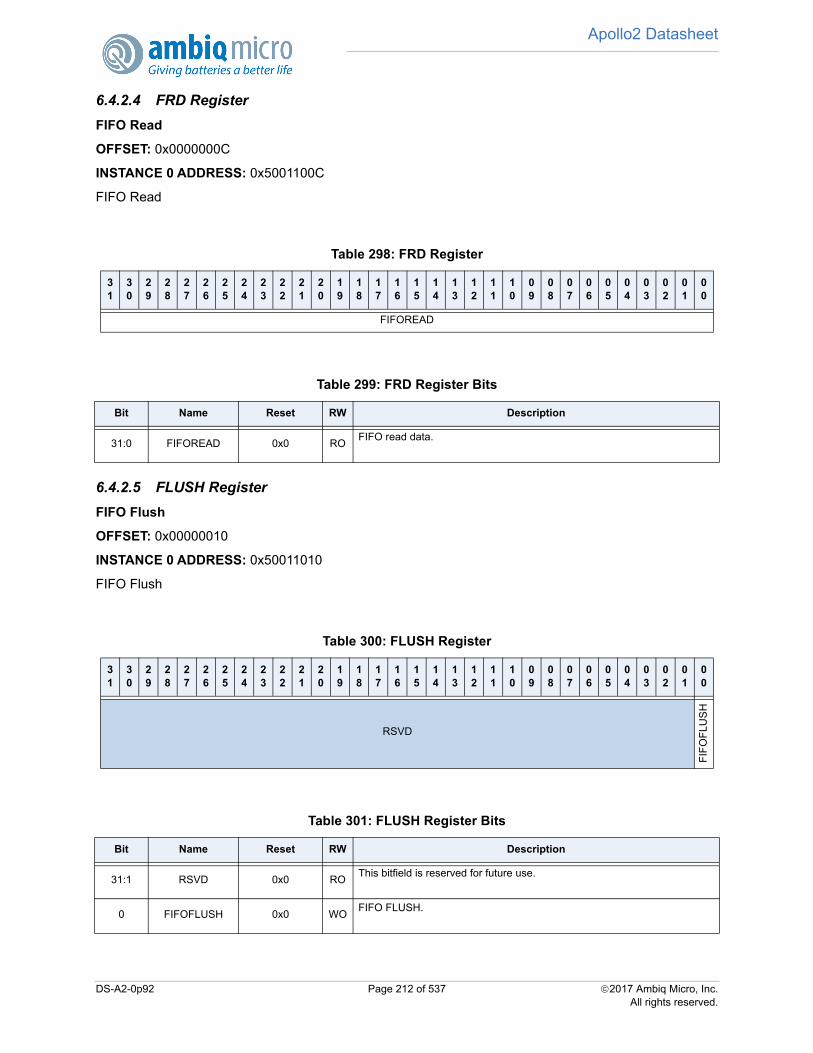
Apollo2 Datasheet
6.4.2.4 FRD Register
FIFO Read
OFFSET: 0x0000000C
INSTANCE 0 ADDRESS: 0x5001100C
FIFO Read
6.4.2.5 FLUSH Register
FIFO Flush
OFFSET: 0x00000010
INSTANCE 0 ADDRESS: 0x50011010
FIFO Flush
Table 298: FRD Register
31
30
29
28
27
26
25
24
23
22
21
20
19
18
17
16
15
14
13
12
11
10
09
08
07
06
05
04
03
02
01
00
FIFOREAD
Table 299: FRD Register Bits
Bit Name Reset RW Description
31:0 FIFOREAD 0x0 ROFIFO read data.
Table 300: FLUSH Register
31
30
29
28
27
26
25
24
23
22
21
20
19
18
17
16
15
14
13
12
11
10
09
08
07
06
05
04
03
02
01
00
RSVD
FIF
OF
LUS
H
Table 301: FLUSH Register Bits
Bit Name Reset RW Description
31:1 RSVD 0x0 ROThis bitfield is reserved for future use.
0 FIFOFLUSH 0x0 WOFIFO FLUSH.
DS-A2-0p92 Page 212 of 537 2017 Ambiq Micro, Inc.All rights reserved.
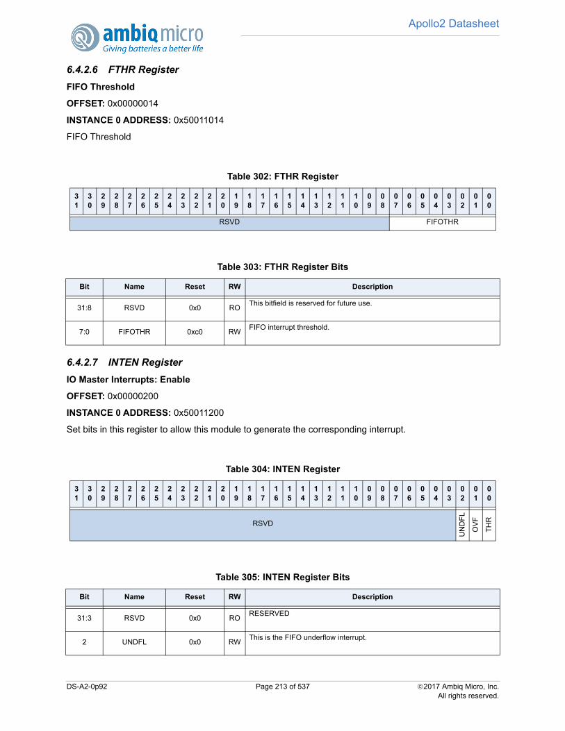
Apollo2 Datasheet
6.4.2.6 FTHR Register
FIFO Threshold
OFFSET: 0x00000014
INSTANCE 0 ADDRESS: 0x50011014
FIFO Threshold
6.4.2.7 INTEN Register
IO Master Interrupts: Enable
OFFSET: 0x00000200
INSTANCE 0 ADDRESS: 0x50011200
Set bits in this register to allow this module to generate the corresponding interrupt.
Table 302: FTHR Register
31
30
29
28
27
26
25
24
23
22
21
20
19
18
17
16
15
14
13
12
11
10
09
08
07
06
05
04
03
02
01
00
RSVD FIFOTHR
Table 303: FTHR Register Bits
Bit Name Reset RW Description
31:8 RSVD 0x0 ROThis bitfield is reserved for future use.
7:0 FIFOTHR 0xc0 RWFIFO interrupt threshold.
Table 304: INTEN Register
31
30
29
28
27
26
25
24
23
22
21
20
19
18
17
16
15
14
13
12
11
10
09
08
07
06
05
04
03
02
01
00
RSVD
UN
DF
L
OV
F
TH
R
Table 305: INTEN Register Bits
Bit Name Reset RW Description
31:3 RSVD 0x0 RORESERVED
2 UNDFL 0x0 RWThis is the FIFO underflow interrupt.
DS-A2-0p92 Page 213 of 537 2017 Ambiq Micro, Inc.All rights reserved.
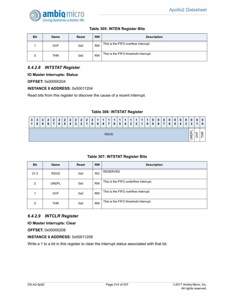
Apollo2 Datasheet
6.4.2.8 INTSTAT Register
IO Master Interrupts: Status
OFFSET: 0x00000204
INSTANCE 0 ADDRESS: 0x50011204
Read bits from this register to discover the cause of a recent interrupt.
6.4.2.9 INTCLR Register
IO Master Interrupts: Clear
OFFSET: 0x00000208
INSTANCE 0 ADDRESS: 0x50011208
Write a 1 to a bit in this register to clear the interrupt status associated with that bit.
1 OVF 0x0 RWThis is the FIFO overflow interrupt.
0 THR 0x0 RWThis is the FIFO threshold interrupt.
Table 306: INTSTAT Register
31
30
29
28
27
26
25
24
23
22
21
20
19
18
17
16
15
14
13
12
11
10
09
08
07
06
05
04
03
02
01
00
RSVD
UN
DF
L
OV
F
TH
R
Table 307: INTSTAT Register Bits
Bit Name Reset RW Description
31:3 RSVD 0x0 RORESERVED
2 UNDFL 0x0 RWThis is the FIFO underflow interrupt.
1 OVF 0x0 RWThis is the FIFO overflow interrupt.
0 THR 0x0 RWThis is the FIFO threshold interrupt.
Table 305: INTEN Register Bits
Bit Name Reset RW Description
DS-A2-0p92 Page 214 of 537 2017 Ambiq Micro, Inc.All rights reserved.
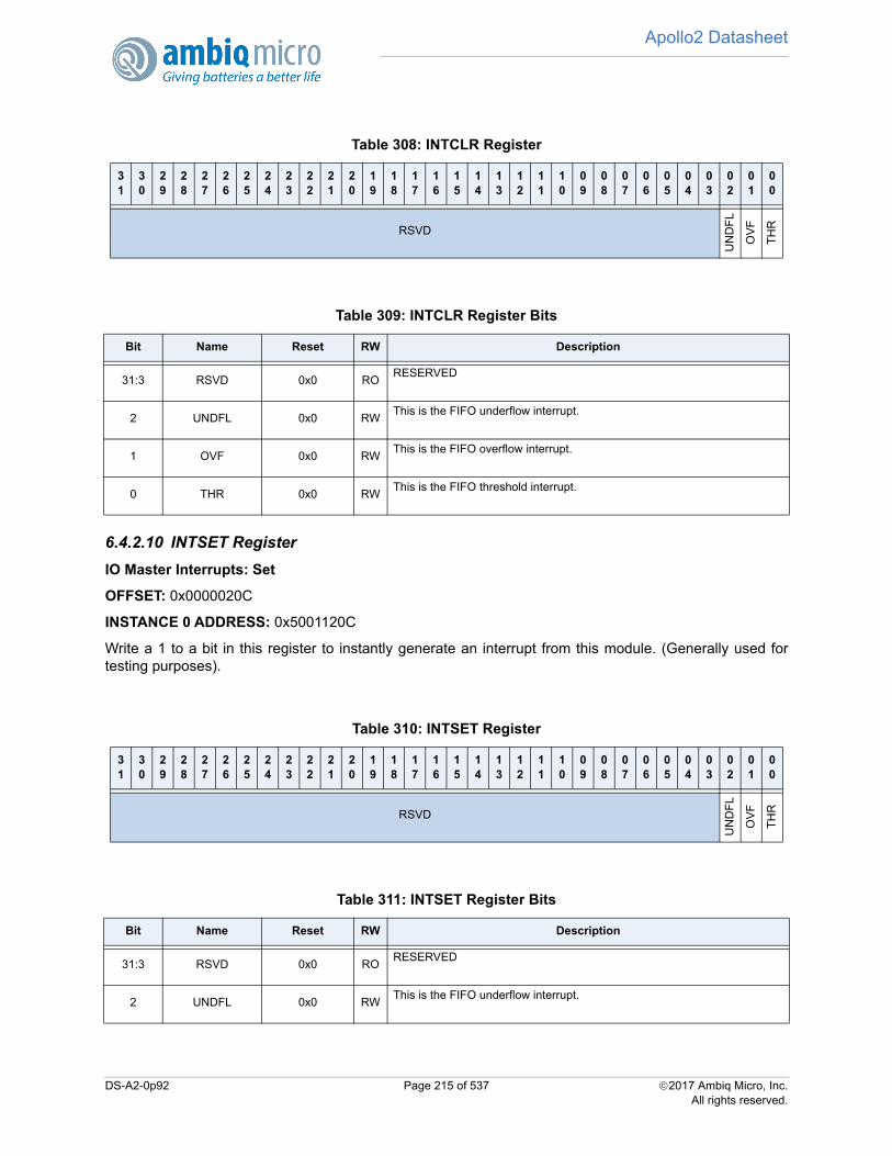
Apollo2 Datasheet
6.4.2.10 INTSET Register
IO Master Interrupts: Set
OFFSET: 0x0000020C
INSTANCE 0 ADDRESS: 0x5001120C
Write a 1 to a bit in this register to instantly generate an interrupt from this module. (Generally used fortesting purposes).
Table 308: INTCLR Register
31
30
29
28
27
26
25
24
23
22
21
20
19
18
17
16
15
14
13
12
11
10
09
08
07
06
05
04
03
02
01
00
RSVD
UN
DF
L
OV
F
TH
R
Table 309: INTCLR Register Bits
Bit Name Reset RW Description
31:3 RSVD 0x0 RORESERVED
2 UNDFL 0x0 RWThis is the FIFO underflow interrupt.
1 OVF 0x0 RWThis is the FIFO overflow interrupt.
0 THR 0x0 RWThis is the FIFO threshold interrupt.
Table 310: INTSET Register
31
30
29
28
27
26
25
24
23
22
21
20
19
18
17
16
15
14
13
12
11
10
09
08
07
06
05
04
03
02
01
00
RSVD
UN
DF
L
OV
F
TH
R
Table 311: INTSET Register Bits
Bit Name Reset RW Description
31:3 RSVD 0x0 RORESERVED
2 UNDFL 0x0 RWThis is the FIFO underflow interrupt.
DS-A2-0p92 Page 215 of 537 2017 Ambiq Micro, Inc.All rights reserved.
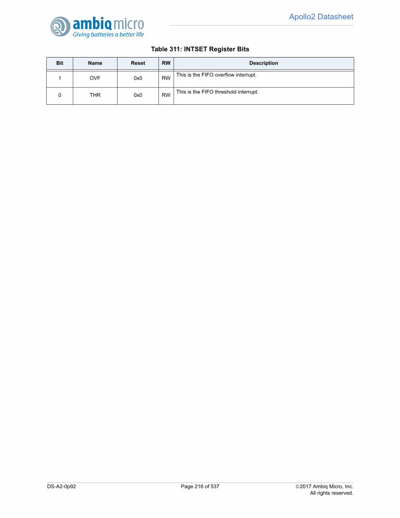
Apollo2 Datasheet
1 OVF 0x0 RWThis is the FIFO overflow interrupt.
0 THR 0x0 RWThis is the FIFO threshold interrupt.
Table 311: INTSET Register Bits
Bit Name Reset RW Description
DS-A2-0p92 Page 216 of 537 2017 Ambiq Micro, Inc.All rights reserved.
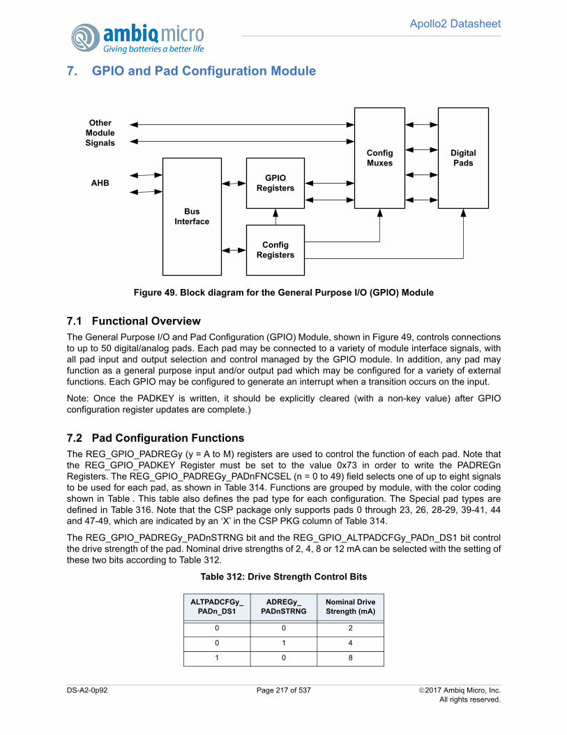
Apollo2 Datasheet
7. GPIO and Pad Configuration Module
Figure 49. Block diagram for the General Purpose I/O (GPIO) Module
7.1 Functional OverviewThe General Purpose I/O and Pad Configuration (GPIO) Module, shown in Figure 49, controls connectionsto up to 50 digital/analog pads. Each pad may be connected to a variety of module interface signals, withall pad input and output selection and control managed by the GPIO module. In addition, any pad mayfunction as a general purpose input and/or output pad which may be configured for a variety of externalfunctions. Each GPIO may be configured to generate an interrupt when a transition occurs on the input.
Note: Once the PADKEY is written, it should be explicitly cleared (with a non-key value) after GPIOconfiguration register updates are complete.)
7.2 Pad Configuration FunctionsThe REG_GPIO_PADREGy (y = A to M) registers are used to control the function of each pad. Note thatthe REG_GPIO_PADKEY Register must be set to the value 0x73 in order to write the PADREGnRegisters. The REG_GPIO_PADREGy_PADnFNCSEL (n = 0 to 49) field selects one of up to eight signalsto be used for each pad, as shown in Table 314. Functions are grouped by module, with the color codingshown in Table . This table also defines the pad type for each configuration. The Special pad types aredefined in Table 316. Note that the CSP package only supports pads 0 through 23, 26, 28-29, 39-41, 44and 47-49, which are indicated by an ‘X’ in the CSP PKG column of Table 314.
The REG_GPIO_PADREGy_PADnSTRNG bit and the REG_GPIO_ALTPADCFGy_PADn_DS1 bit controlthe drive strength of the pad. Nominal drive strengths of 2, 4, 8 or 12 mA can be selected with the setting ofthese two bits according to Table 312.
Table 312: Drive Strength Control Bits
ALTPADCFGy_PADn_DS1
ADREGy_PADnSTRNG
Nominal Drive Strength (mA)
0 0 2
0 1 4
1 0 8
GPIO Registers
Config Registers
Bus Interface
Digital Pads
Config Muxes
Other Module Signals
AHB
DS-A2-0p92 Page 217 of 537 2017 Ambiq Micro, Inc.All rights reserved.
Apollo2 Datasheet
For all pads except for pad 20, REG_GPIO_PADREGy_PADnPULL bit enables a weak pull-up on the padwhen set to one. For pad 20, the REG_GPIO_PADREGy_PAD20PULL bit enables a weak pull-down onthe pad when set to one. The REG_GPIO_PADREGy_PADnINPEN bit must be set to enable the padinput, and should be left clear whenever the pad is not used in order to eliminate any leakage current in thepad.
Pads 22 and 41 have selectable high side power switch transistors to provide ~1 Ω switches to VDDH.Pad 4 has a selectable low side power switch transistor to provide a ~1 Ω switch to VSS. The high sidepower switches are enabled by setting the REG_GPIO_PADREGF_PAD22PWRUP orREG_GPIO_PADREGK_PAD41PWRUP bits, and the low side switch is enabled by setting theREG_GPIO_PADREGB_PAD4PWRDN bit. Once enabled, the switches operate in parallel with the normalpad function.
Pads 0, 1, 5, 6, 8, 9, 25, 27, 39, 40, 42, 43, 48 and 49 include optional pull-up resistors for use in I2C mode,to eliminate the need for external resistors. If the pull-up is enabled by the PADnPULL bit, theREG_GPIO_PADREGy_PADnRSEL field selects the size of the pull-up resistor as shown in Table 317.
.
1 1 12
ALTPADCFGy_PADn_DS1
ADREGy_PADnSTRNG
Nominal Drive Strength (mA)
DS-A2-0p92 Page 218 of 537 2017 Ambiq Micro, Inc.All rights reserved.
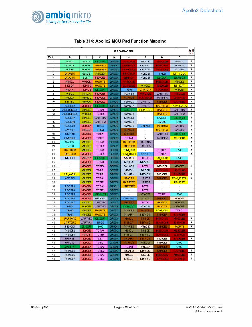
Apollo2 Datasheet
Table 314: Apollo2 MCU Pad Function Mapping
DS-A2-0p92 Page 219 of 537 2017 Ambiq Micro, Inc.All rights reserved.
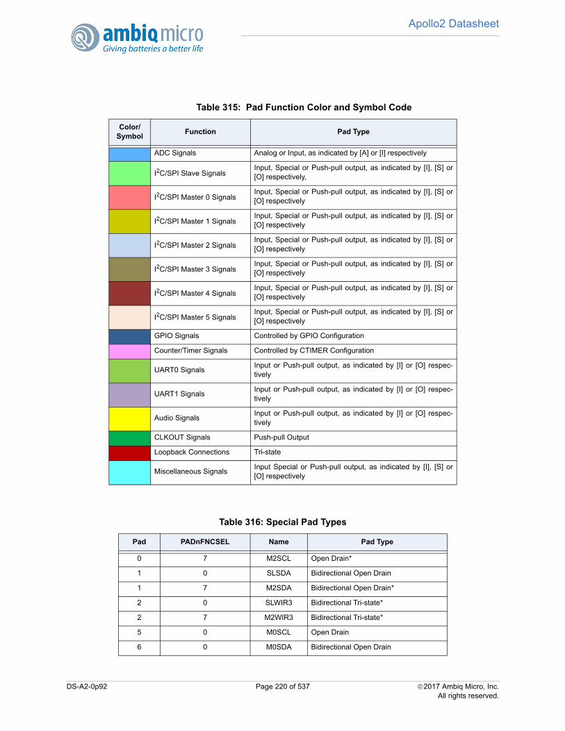
Apollo2 Datasheet
Table 315: Pad Function Color and Symbol Code
Color/Symbol
Function Pad Type
ADC Signals Analog or Input, as indicated by [A] or [I] respectively
I2C/SPI Slave SignalsInput, Special or Push-pull output, as indicated by [I], [S] or[O] respectively,
I2C/SPI Master 0 SignalsInput, Special or Push-pull output, as indicated by [I], [S] or[O] respectively
I2C/SPI Master 1 SignalsInput, Special or Push-pull output, as indicated by [I], [S] or[O] respectively
I2C/SPI Master 2 SignalsInput, Special or Push-pull output, as indicated by [I], [S] or[O] respectively
I2C/SPI Master 3 SignalsInput, Special or Push-pull output, as indicated by [I], [S] or[O] respectively
I2C/SPI Master 4 SignalsInput, Special or Push-pull output, as indicated by [I], [S] or[O] respectively
I2C/SPI Master 5 SignalsInput, Special or Push-pull output, as indicated by [I], [S] or[O] respectively
GPIO Signals Controlled by GPIO Configuration
Counter/Timer Signals Controlled by CTIMER Configuration
UART0 SignalsInput or Push-pull output, as indicated by [I] or [O] respec-tively
UART1 SignalsInput or Push-pull output, as indicated by [I] or [O] respec-tively
Audio SignalsInput or Push-pull output, as indicated by [I] or [O] respec-tively
CLKOUT Signals Push-pull Output
Loopback Connections Tri-state
Miscellaneous SignalsInput Special or Push-pull output, as indicated by [I], [S] or[O] respectively
Table 316: Special Pad Types
Pad PADnFNCSEL Name Pad Type
0 7 M2SCL Open Drain*
1 0 SLSDA Bidirectional Open Drain
1 7 M2SDA Bidirectional Open Drain*
2 0 SLWIR3 Bidirectional Tri-state*
2 7 M2WIR3 Bidirectional Tri-state*
5 0 M0SCL Open Drain
6 0 M0SDA Bidirectional Open Drain
DS-A2-0p92 Page 220 of 537 2017 Ambiq Micro, Inc.All rights reserved.
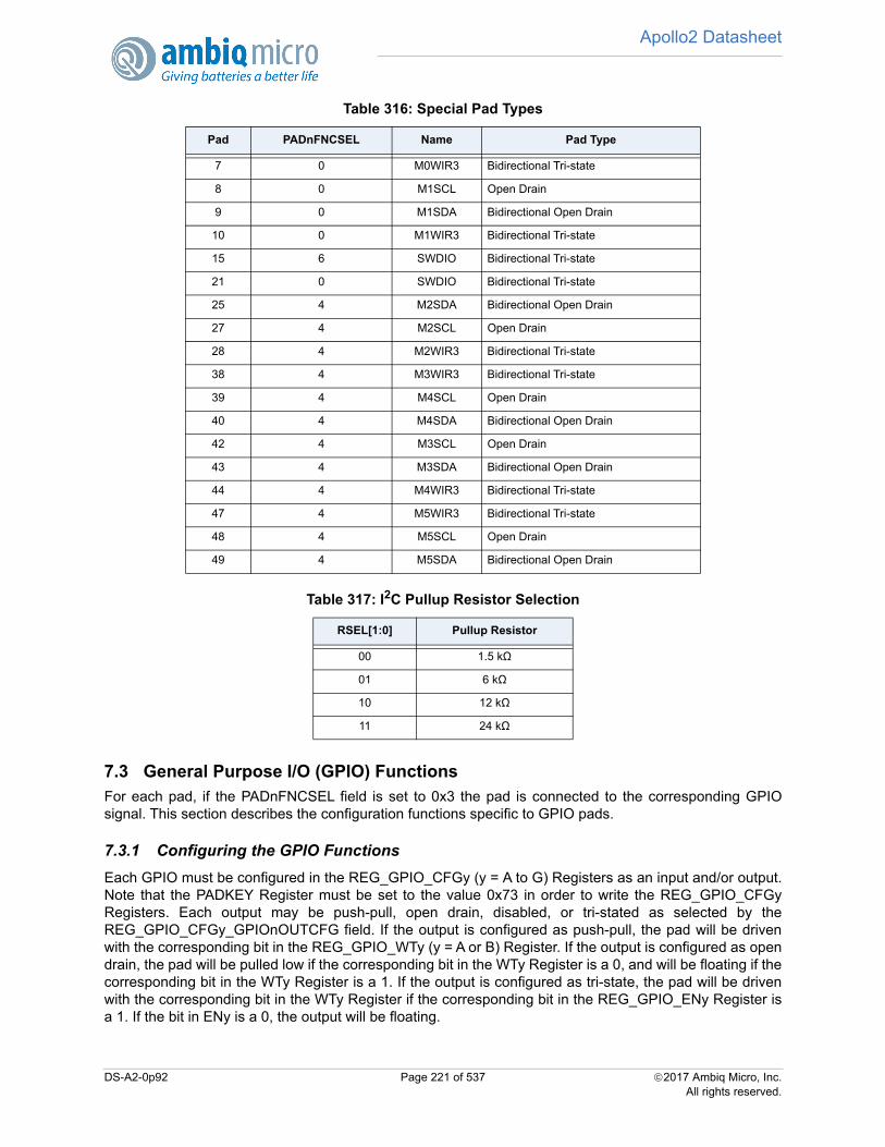
Apollo2 Datasheet
7.3 General Purpose I/O (GPIO) FunctionsFor each pad, if the PADnFNCSEL field is set to 0x3 the pad is connected to the corresponding GPIOsignal. This section describes the configuration functions specific to GPIO pads.
7.3.1 Configuring the GPIO Functions
Each GPIO must be configured in the REG_GPIO_CFGy (y = A to G) Registers as an input and/or output.Note that the PADKEY Register must be set to the value 0x73 in order to write the REG_GPIO_CFGyRegisters. Each output may be push-pull, open drain, disabled, or tri-stated as selected by theREG_GPIO_CFGy_GPIOnOUTCFG field. If the output is configured as push-pull, the pad will be drivenwith the corresponding bit in the REG_GPIO_WTy (y = A or B) Register. If the output is configured as opendrain, the pad will be pulled low if the corresponding bit in the WTy Register is a 0, and will be floating if thecorresponding bit in the WTy Register is a 1. If the output is configured as tri-state, the pad will be drivenwith the corresponding bit in the WTy Register if the corresponding bit in the REG_GPIO_ENy Register isa 1. If the bit in ENy is a 0, the output will be floating.
7 0 M0WIR3 Bidirectional Tri-state
8 0 M1SCL Open Drain
9 0 M1SDA Bidirectional Open Drain
10 0 M1WIR3 Bidirectional Tri-state
15 6 SWDIO Bidirectional Tri-state
21 0 SWDIO Bidirectional Tri-state
25 4 M2SDA Bidirectional Open Drain
27 4 M2SCL Open Drain
28 4 M2WIR3 Bidirectional Tri-state
38 4 M3WIR3 Bidirectional Tri-state
39 4 M4SCL Open Drain
40 4 M4SDA Bidirectional Open Drain
42 4 M3SCL Open Drain
43 4 M3SDA Bidirectional Open Drain
44 4 M4WIR3 Bidirectional Tri-state
47 4 M5WIR3 Bidirectional Tri-state
48 4 M5SCL Open Drain
49 4 M5SDA Bidirectional Open Drain
Table 317: I2C Pullup Resistor Selection
RSEL[1:0] Pullup Resistor
00 1.5 kΩ
01 6 kΩ
10 12 kΩ
11 24 kΩ
Table 316: Special Pad Types
Pad PADnFNCSEL Name Pad Type
DS-A2-0p92 Page 221 of 537 2017 Ambiq Micro, Inc.All rights reserved.
Apollo2 Datasheet
7.3.2 Reading from a GPIO Pad
All GPIO inputs are readable at all times, even if the pad is not configured as a GPIO. The current valuesof pads 0 to 31 are read in the REG_GPIO_RDA Register, and the current values of pads 32 to 49 are readin the REG_GPIO_RDB Register. If the REG_GPIO_CFGy_GPIOnINCFG bit is set for a GPIO, it willalways read as zero.
7.3.3 Writing to a GPIO Pad
The GPIO pad outputs are controlled by the REG_GPIO_WTA/B Registers and the REG_GPIO_ENA/BRegisters. Each of these registers may be directly written and read. Because each GPIO is often anindependent function, the capability also exists to set or clear one or more bits without having to perform aread-modify-write operation. If the REG_GPIO_WTSA or REG_GPIO_WTSB Register is written, thecorresponding bit in WTA/B will be set if the write data is 1, otherwise the WTA/B bit will not be changed. Ifthe REG_GPIO_WTCA or REG_GPIO_WTCB Register is written, the corresponding bit in WTA/B will becleared if the write data is 1, otherwise the WTA/B bit will not be changed.
If a GPIO pad is configured for tri-state output mode, the ENA/B Register controls the enabling of each bit.ENA and ENB may be directly written, and individual bits may be set or cleared by writing the ENSA/B orENCA/B Registers with a 1 in the desired bit position.
7.3.4 GPIO Interrupts
Each GPIO pad can be configured to generate an interrupt on a high-to-low transition or a low-to-hightransition, as selected by the REG_GPIO_CFGy_GPIOnINTD bit. This interrupt will be generated even ifthe pad is not configured as a GPIO in the Pad Configuration logic. Each interrupt is enabled, disabled,cleared or set with a standard set of Interrupt Registers GPIOA_IER, GPIOA_ISR, GPIOA_WCR andGPIOB_WSR for GPIO pads 0 to 31, and Registers GPIOB_IER, GPIOB_ISR, GPIOB_WCR andGPIOB_WSR for GPIO pads 32 to 49.
7.4 Pad Connection Summary
Figure 50 shows the detailed implementation of each pad. Each element will be described in detail.
7.4.1 Output Selection
There is multiplexer which selects the module signal to be driven to the output based onREG_GPIO_PADREGy_PADnFNCSEL field. This implements the multiplexing shown in Table 314 foroutput pads. For all pads, a PADnFNCSEL value of 0x3 selects the value in the corresponding GPIO_WTyregister bit.
7.4.2 Output Control
The pad driver for each pad has a data input and an output enable input. Each of these controls is selectedfrom among several alternatives based on the OUTDATSEL and OUTENSEL signals which are controlledby the selection of the output type as shown in Table 316 and Table 317.
OUTDATSEL normally selects the data from the output multiplexer, but if the pad is configured as OpenDrain the data input is selected to be low.
DS-A2-0p92 Page 222 of 537 2017 Ambiq Micro, Inc.All rights reserved.
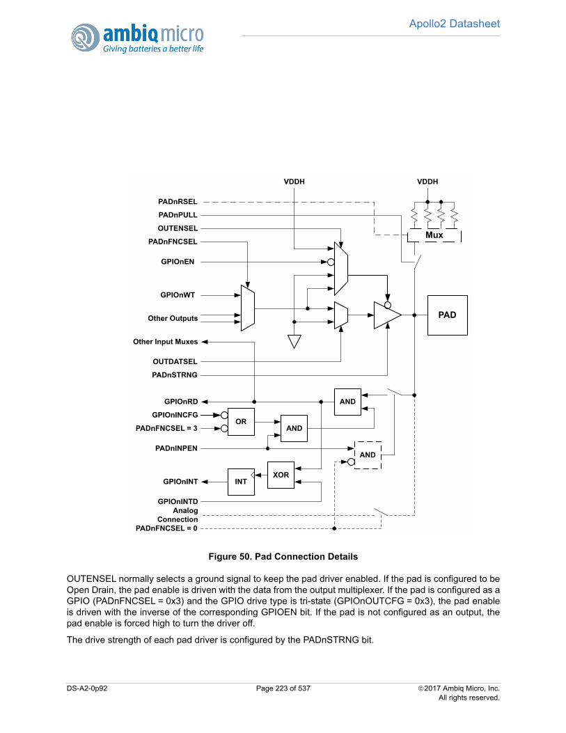
Apollo2 Datasheet
Figure 50. Pad Connection Details
OUTENSEL normally selects a ground signal to keep the pad driver enabled. If the pad is configured to beOpen Drain, the pad enable is driven with the data from the output multiplexer. If the pad is configured as aGPIO (PADnFNCSEL = 0x3) and the GPIO drive type is tri-state (GPIOnOUTCFG = 0x3), the pad enableis driven with the inverse of the corresponding GPIOEN bit. If the pad is not configured as an output, thepad enable is forced high to turn the driver off.
The drive strength of each pad driver is configured by the PADnSTRNG bit.
PAD
PADnFNCSEL
AND
GPIOnWT
GPIOnEN
Other Outputs
OUTENSEL
OUTDATSEL
PADnINPEN
ANDOR
GPIOnRD
PADnFNCSEL = 3
GPIOnINCFG
Other Input Muxes
XORINTGPIOnINT
GPIOnINTDAnalog
ConnectionPADnFNCSEL = 0
PADnPULL
Mux
VDDH
PADnRSEL
VDDH
PADnSTRNG
AND
DS-A2-0p92 Page 223 of 537 2017 Ambiq Micro, Inc.All rights reserved.
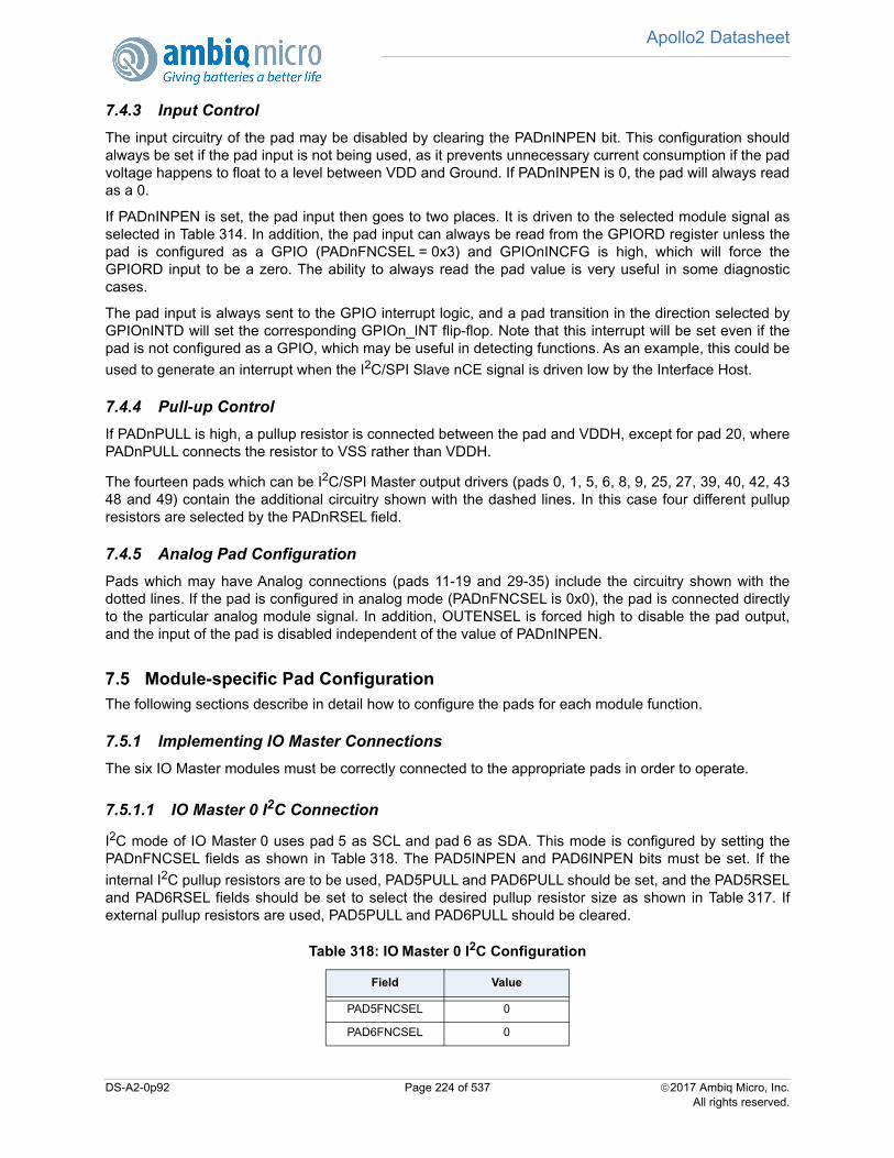
Apollo2 Datasheet
7.4.3 Input Control
The input circuitry of the pad may be disabled by clearing the PADnINPEN bit. This configuration shouldalways be set if the pad input is not being used, as it prevents unnecessary current consumption if the padvoltage happens to float to a level between VDD and Ground. If PADnINPEN is 0, the pad will always readas a 0.
If PADnINPEN is set, the pad input then goes to two places. It is driven to the selected module signal asselected in Table 314. In addition, the pad input can always be read from the GPIORD register unless thepad is configured as a GPIO (PADnFNCSEL = 0x3) and GPIOnINCFG is high, which will force theGPIORD input to be a zero. The ability to always read the pad value is very useful in some diagnosticcases.
The pad input is always sent to the GPIO interrupt logic, and a pad transition in the direction selected byGPIOnINTD will set the corresponding GPIOn_INT flip-flop. Note that this interrupt will be set even if thepad is not configured as a GPIO, which may be useful in detecting functions. As an example, this could be
used to generate an interrupt when the I2C/SPI Slave nCE signal is driven low by the Interface Host.
7.4.4 Pull-up Control
If PADnPULL is high, a pullup resistor is connected between the pad and VDDH, except for pad 20, wherePADnPULL connects the resistor to VSS rather than VDDH.
The fourteen pads which can be I2C/SPI Master output drivers (pads 0, 1, 5, 6, 8, 9, 25, 27, 39, 40, 42, 4348 and 49) contain the additional circuitry shown with the dashed lines. In this case four different pullupresistors are selected by the PADnRSEL field.
7.4.5 Analog Pad Configuration
Pads which may have Analog connections (pads 11-19 and 29-35) include the circuitry shown with thedotted lines. If the pad is configured in analog mode (PADnFNCSEL is 0x0), the pad is connected directlyto the particular analog module signal. In addition, OUTENSEL is forced high to disable the pad output,and the input of the pad is disabled independent of the value of PADnINPEN.
7.5 Module-specific Pad ConfigurationThe following sections describe in detail how to configure the pads for each module function.
7.5.1 Implementing IO Master Connections
The six IO Master modules must be correctly connected to the appropriate pads in order to operate.
7.5.1.1 IO Master 0 I2C Connection
I2C mode of IO Master 0 uses pad 5 as SCL and pad 6 as SDA. This mode is configured by setting thePADnFNCSEL fields as shown in Table 318. The PAD5INPEN and PAD6INPEN bits must be set. If the
internal I2C pullup resistors are to be used, PAD5PULL and PAD6PULL should be set, and the PAD5RSELand PAD6RSEL fields should be set to select the desired pullup resistor size as shown in Table 317. Ifexternal pullup resistors are used, PAD5PULL and PAD6PULL should be cleared.
Table 318: IO Master 0 I2C Configuration
Field Value
PAD5FNCSEL 0
PAD6FNCSEL 0
DS-A2-0p92 Page 224 of 537 2017 Ambiq Micro, Inc.All rights reserved.
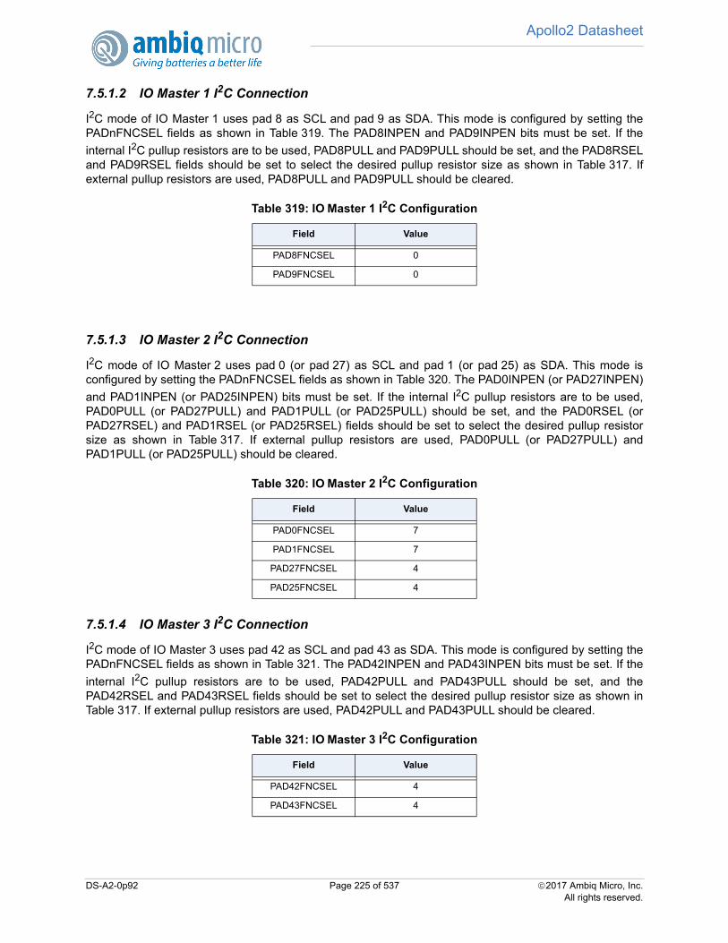
Apollo2 Datasheet
7.5.1.2 IO Master 1 I2C Connection
I2C mode of IO Master 1 uses pad 8 as SCL and pad 9 as SDA. This mode is configured by setting thePADnFNCSEL fields as shown in Table 319. The PAD8INPEN and PAD9INPEN bits must be set. If the
internal I2C pullup resistors are to be used, PAD8PULL and PAD9PULL should be set, and the PAD8RSELand PAD9RSEL fields should be set to select the desired pullup resistor size as shown in Table 317. Ifexternal pullup resistors are used, PAD8PULL and PAD9PULL should be cleared.
7.5.1.3 IO Master 2 I2C Connection
I2C mode of IO Master 2 uses pad 0 (or pad 27) as SCL and pad 1 (or pad 25) as SDA. This mode isconfigured by setting the PADnFNCSEL fields as shown in Table 320. The PAD0INPEN (or PAD27INPEN)
and PAD1INPEN (or PAD25INPEN) bits must be set. If the internal I2C pullup resistors are to be used,PAD0PULL (or PAD27PULL) and PAD1PULL (or PAD25PULL) should be set, and the PAD0RSEL (orPAD27RSEL) and PAD1RSEL (or PAD25RSEL) fields should be set to select the desired pullup resistorsize as shown in Table 317. If external pullup resistors are used, PAD0PULL (or PAD27PULL) andPAD1PULL (or PAD25PULL) should be cleared.
7.5.1.4 IO Master 3 I2C Connection
I2C mode of IO Master 3 uses pad 42 as SCL and pad 43 as SDA. This mode is configured by setting thePADnFNCSEL fields as shown in Table 321. The PAD42INPEN and PAD43INPEN bits must be set. If the
internal I2C pullup resistors are to be used, PAD42PULL and PAD43PULL should be set, and thePAD42RSEL and PAD43RSEL fields should be set to select the desired pullup resistor size as shown inTable 317. If external pullup resistors are used, PAD42PULL and PAD43PULL should be cleared.
Table 319: IO Master 1 I2C Configuration
Field Value
PAD8FNCSEL 0
PAD9FNCSEL 0
Table 320: IO Master 2 I2C Configuration
Field Value
PAD0FNCSEL 7
PAD1FNCSEL 7
PAD27FNCSEL 4
PAD25FNCSEL 4
Table 321: IO Master 3 I2C Configuration
Field Value
PAD42FNCSEL 4
PAD43FNCSEL 4
DS-A2-0p92 Page 225 of 537 2017 Ambiq Micro, Inc.All rights reserved.
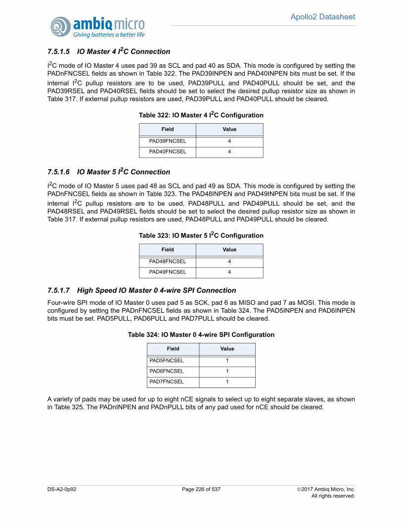
Apollo2 Datasheet
7.5.1.5 IO Master 4 I2C Connection
I2C mode of IO Master 4 uses pad 39 as SCL and pad 40 as SDA. This mode is configured by setting thePADnFNCSEL fields as shown in Table 322. The PAD39INPEN and PAD40INPEN bits must be set. If the
internal I2C pullup resistors are to be used, PAD39PULL and PAD40PULL should be set, and thePAD39RSEL and PAD40RSEL fields should be set to select the desired pullup resistor size as shown inTable 317. If external pullup resistors are used, PAD39PULL and PAD40PULL should be cleared.
7.5.1.6 IO Master 5 I2C Connection
I2C mode of IO Master 5 uses pad 48 as SCL and pad 49 as SDA. This mode is configured by setting thePADnFNCSEL fields as shown in Table 323. The PAD48INPEN and PAD49INPEN bits must be set. If the
internal I2C pullup resistors are to be used, PAD48PULL and PAD49PULL should be set, and thePAD48RSEL and PAD49RSEL fields should be set to select the desired pullup resistor size as shown inTable 317. If external pullup resistors are used, PAD48PULL and PAD49PULL should be cleared.
7.5.1.7 High Speed IO Master 0 4-wire SPI Connection
Four-wire SPI mode of IO Master 0 uses pad 5 as SCK, pad 6 as MISO and pad 7 as MOSI. This mode isconfigured by setting the PADnFNCSEL fields as shown in Table 324. The PAD5INPEN and PAD6INPENbits must be set. PAD5PULL, PAD6PULL and PAD7PULL should be cleared.
A variety of pads may be used for up to eight nCE signals to select up to eight separate slaves, as shownin Table 325. The PADnINPEN and PADnPULL bits of any pad used for nCE should be cleared.
Table 322: IO Master 4 I2C Configuration
Field Value
PAD39FNCSEL 4
PAD40FNCSEL 4
Table 323: IO Master 5 I2C Configuration
Field Value
PAD48FNCSEL 4
PAD49FNCSEL 4
Table 324: IO Master 0 4-wire SPI Configuration
Field Value
PAD5FNCSEL 1
PAD6FNCSEL 1
PAD7FNCSEL 1
DS-A2-0p92 Page 226 of 537 2017 Ambiq Micro, Inc.All rights reserved.
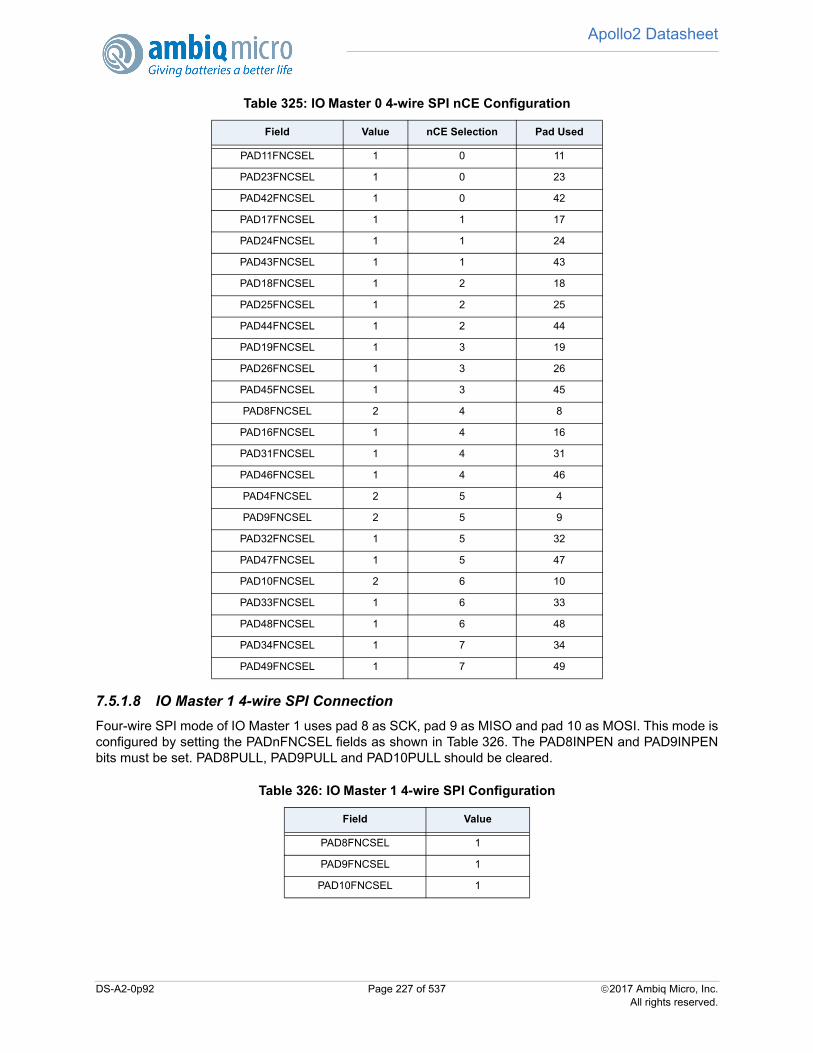
Apollo2 Datasheet
7.5.1.8 IO Master 1 4-wire SPI Connection
Four-wire SPI mode of IO Master 1 uses pad 8 as SCK, pad 9 as MISO and pad 10 as MOSI. This mode isconfigured by setting the PADnFNCSEL fields as shown in Table 326. The PAD8INPEN and PAD9INPENbits must be set. PAD8PULL, PAD9PULL and PAD10PULL should be cleared.
Table 325: IO Master 0 4-wire SPI nCE Configuration
Field Value nCE Selection Pad Used
PAD11FNCSEL 1 0 11
PAD23FNCSEL 1 0 23
PAD42FNCSEL 1 0 42
PAD17FNCSEL 1 1 17
PAD24FNCSEL 1 1 24
PAD43FNCSEL 1 1 43
PAD18FNCSEL 1 2 18
PAD25FNCSEL 1 2 25
PAD44FNCSEL 1 2 44
PAD19FNCSEL 1 3 19
PAD26FNCSEL 1 3 26
PAD45FNCSEL 1 3 45
PAD8FNCSEL 2 4 8
PAD16FNCSEL 1 4 16
PAD31FNCSEL 1 4 31
PAD46FNCSEL 1 4 46
PAD4FNCSEL 2 5 4
PAD9FNCSEL 2 5 9
PAD32FNCSEL 1 5 32
PAD47FNCSEL 1 5 47
PAD10FNCSEL 2 6 10
PAD33FNCSEL 1 6 33
PAD48FNCSEL 1 6 48
PAD34FNCSEL 1 7 34
PAD49FNCSEL 1 7 49
Table 326: IO Master 1 4-wire SPI Configuration
Field Value
PAD8FNCSEL 1
PAD9FNCSEL 1
PAD10FNCSEL 1
DS-A2-0p92 Page 227 of 537 2017 Ambiq Micro, Inc.All rights reserved.
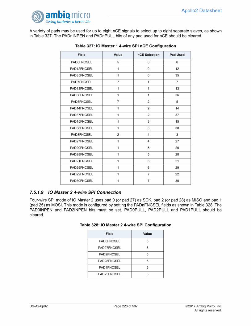
Apollo2 Datasheet
A variety of pads may be used for up to eight nCE signals to select up to eight separate slaves, as shownin Table 327. The PADnINPEN and PADnPULL bits of any pad used for nCE should be cleared.
7.5.1.9 IO Master 2 4-wire SPI Connection
Four-wire SPI mode of IO Master 2 uses pad 0 (or pad 27) as SCK, pad 2 (or pad 28) as MISO and pad 1(pad 25) as MOSI. This mode is configured by setting the PADnFNCSEL fields as shown in Table 328. ThePAD0INPEN and PAD2INPEN bits must be set. PAD0PULL, PAD2PULL and PAD1PULL should becleared.
Table 327: IO Master 1 4-wire SPI nCE Configuration
Field Value nCE Selection Pad Used
PAD6FNCSEL 5 0 6
PAD12FNCSEL 1 0 12
PAD35FNCSEL 1 0 35
PAD7FNCSEL 7 1 7
PAD13FNCSEL 1 1 13
PAD36FNCSEL 1 1 36
PAD5FNCSEL 7 2 5
PAD14FNCSEL 1 2 14
PAD37FNCSEL 1 2 37
PAD15FNCSEL 1 3 15
PAD38FNCSEL 1 3 38
PAD3FNCSEL 2 4 3
PAD27FNCSEL 1 4 27
PAD20FNCSEL 1 5 20
PAD28FNCSEL 1 5 28
PAD21FNCSEL 1 6 21
PAD29FNCSEL 1 6 29
PAD22FNCSEL 1 7 22
PAD30FNCSEL 1 7 30
Table 328: IO Master 2 4-wire SPI Configuration
Field Value
PAD0FNCSEL 5
PAD27FNCSEL 5
PAD2FNCSEL 5
PAD28FNCSEL 5
PAD1FNCSEL 5
PAD25FNCSEL 5
DS-A2-0p92 Page 228 of 537 2017 Ambiq Micro, Inc.All rights reserved.

Apollo2 Datasheet
A variety of pads may be used for up to eight nCE signals to select up to eight separate slaves, as shownin Table 329. The PADnINPEN and PADnPULL bits of any pad used for nCE should be cleared.
7.5.1.10 IO Master 3 4-wire SPI Connection
Four-wire SPI mode of IO Master 3 uses pad 42 as SCK, pad 43 as MISO and pad 38 as MOSI. This modeis configured by setting the PADnFNCSEL fields as shown in Table 330. The PAD42INPEN andPAD38INPEN bits must be set. PAD38PULL, PAD42PULL and PAD43PULL should be cleared.
A variety of pads may be used for up to eight nCE signals to select up to eight separate slaves, as shownin Table 331. The PADnINPEN and PADnPULL bits of any pad used for nCE should be cleared.
Table 329: IO Master 2 4-wire SPI nCE Configuration
Field Value nCE Selection Pad Used
PAD3FNCSEL 5 0 3
PAD26FNCSEL 4 0 26
PAD36FNCSEL 5 0 36
PAD14FNCSEL 4 1 14
PAD24FNCSEL 0 1 24
PAD41FNCSEL 0 1 41
PAD15FNCSEL 4 2 15
PAD42FNCSEL 0 2 42
PAD13FNCSEL 4 3 13
PAD16FNCSEL 4 3 16
PAD34FNCSEL 2 3 34
PAD8FNCSEL 4 4 8
PAD43FNCSEL 0 4 43
PAD4FNCSEL 5 5 4
PAD47FNCSEL 0 5 47
PAD10FNCSEL 4 6 10
PAD48FNCSEL 0 6 48
PAD11FNCSEL 4 7 11
PAD49FNCSEL 0 7 49
Table 330: IO Master 3 4-wire SPI Configuration
Field Value
PAD38FNCSEL 5
PAD42FNCSEL 5
PAD43FNCSEL 5
Table 331: IO Master 3 4-wire SPI nCE Configuration
Field Value nCE Selection Pad Used
PAD26FNCSEL 7 0 26
DS-A2-0p92 Page 229 of 537 2017 Ambiq Micro, Inc.All rights reserved.
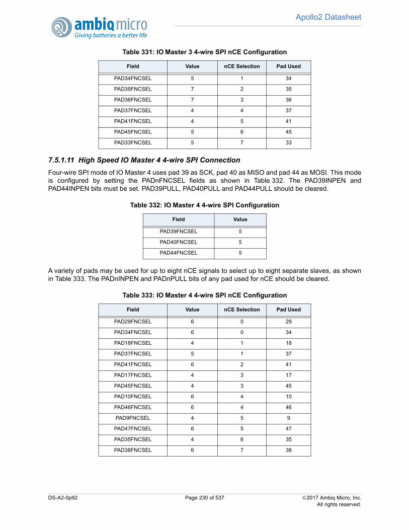
Apollo2 Datasheet
7.5.1.11 High Speed IO Master 4 4-wire SPI Connection
Four-wire SPI mode of IO Master 4 uses pad 39 as SCK, pad 40 as MISO and pad 44 as MOSI. This modeis configured by setting the PADnFNCSEL fields as shown in Table 332. The PAD39INPEN andPAD44INPEN bits must be set. PAD39PULL, PAD40PULL and PAD44PULL should be cleared.
A variety of pads may be used for up to eight nCE signals to select up to eight separate slaves, as shownin Table 333. The PADnINPEN and PADnPULL bits of any pad used for nCE should be cleared.
PAD34FNCSEL 5 1 34
PAD35FNCSEL 7 2 35
PAD36FNCSEL 7 3 36
PAD37FNCSEL 4 4 37
PAD41FNCSEL 4 5 41
PAD45FNCSEL 5 6 45
PAD33FNCSEL 5 7 33
Table 332: IO Master 4 4-wire SPI Configuration
Field Value
PAD39FNCSEL 5
PAD40FNCSEL 5
PAD44FNCSEL 5
Table 333: IO Master 4 4-wire SPI nCE Configuration
Field Value nCE Selection Pad Used
PAD29FNCSEL 6 0 29
PAD34FNCSEL 6 0 34
PAD18FNCSEL 4 1 18
PAD37FNCSEL 5 1 37
PAD41FNCSEL 6 2 41
PAD17FNCSEL 4 3 17
PAD45FNCSEL 4 3 45
PAD10FNCSEL 6 4 10
PAD46FNCSEL 6 4 46
PAD9FNCSEL 4 5 9
PAD47FNCSEL 6 5 47
PAD35FNCSEL 4 6 35
PAD38FNCSEL 6 7 38
Table 331: IO Master 3 4-wire SPI nCE Configuration
Field Value nCE Selection Pad Used
DS-A2-0p92 Page 230 of 537 2017 Ambiq Micro, Inc.All rights reserved.
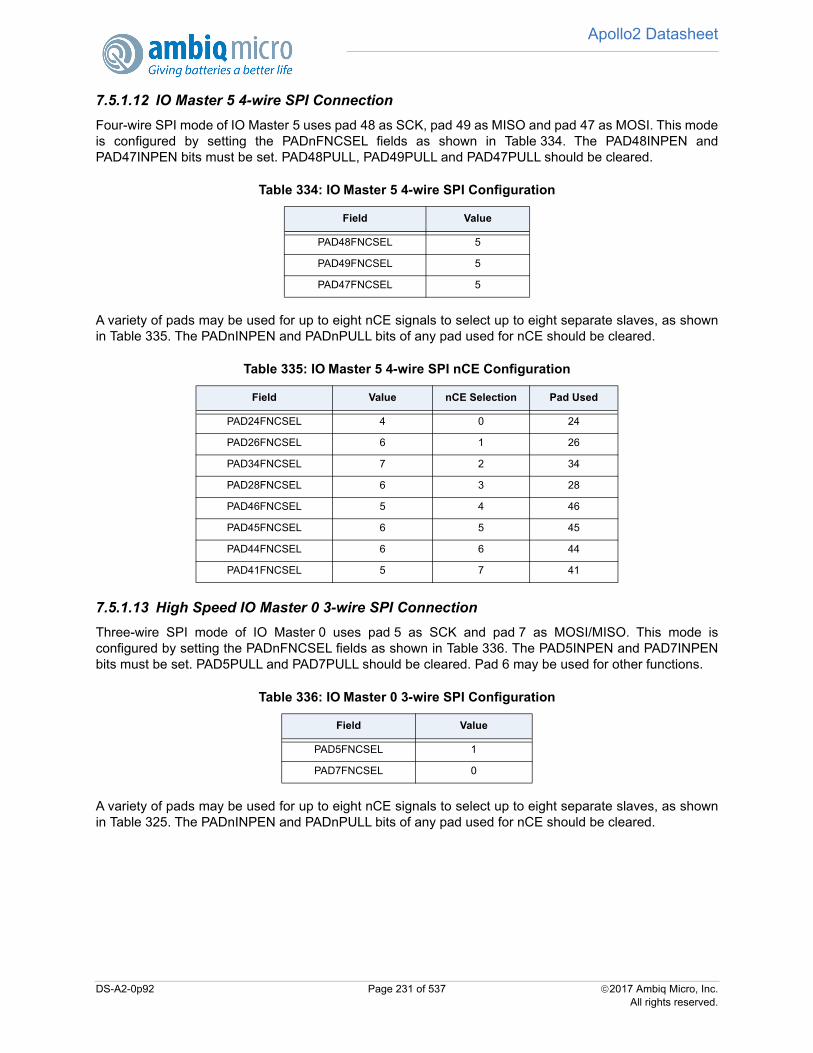
Apollo2 Datasheet
7.5.1.12 IO Master 5 4-wire SPI Connection
Four-wire SPI mode of IO Master 5 uses pad 48 as SCK, pad 49 as MISO and pad 47 as MOSI. This modeis configured by setting the PADnFNCSEL fields as shown in Table 334. The PAD48INPEN andPAD47INPEN bits must be set. PAD48PULL, PAD49PULL and PAD47PULL should be cleared.
A variety of pads may be used for up to eight nCE signals to select up to eight separate slaves, as shownin Table 335. The PADnINPEN and PADnPULL bits of any pad used for nCE should be cleared.
7.5.1.13 High Speed IO Master 0 3-wire SPI Connection
Three-wire SPI mode of IO Master 0 uses pad 5 as SCK and pad 7 as MOSI/MISO. This mode isconfigured by setting the PADnFNCSEL fields as shown in Table 336. The PAD5INPEN and PAD7INPENbits must be set. PAD5PULL and PAD7PULL should be cleared. Pad 6 may be used for other functions.
A variety of pads may be used for up to eight nCE signals to select up to eight separate slaves, as shownin Table 325. The PADnINPEN and PADnPULL bits of any pad used for nCE should be cleared.
Table 334: IO Master 5 4-wire SPI Configuration
Field Value
PAD48FNCSEL 5
PAD49FNCSEL 5
PAD47FNCSEL 5
Table 335: IO Master 5 4-wire SPI nCE Configuration
Field Value nCE Selection Pad Used
PAD24FNCSEL 4 0 24
PAD26FNCSEL 6 1 26
PAD34FNCSEL 7 2 34
PAD28FNCSEL 6 3 28
PAD46FNCSEL 5 4 46
PAD45FNCSEL 6 5 45
PAD44FNCSEL 6 6 44
PAD41FNCSEL 5 7 41
Table 336: IO Master 0 3-wire SPI Configuration
Field Value
PAD5FNCSEL 1
PAD7FNCSEL 0
DS-A2-0p92 Page 231 of 537 2017 Ambiq Micro, Inc.All rights reserved.
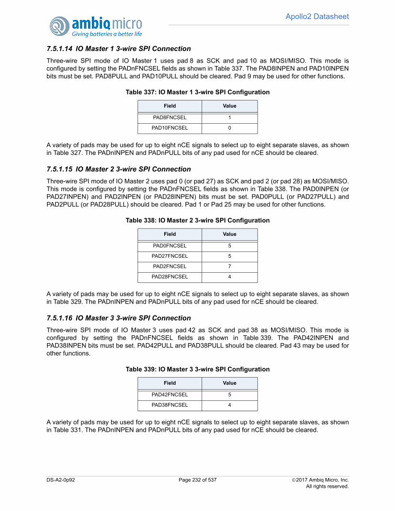
Apollo2 Datasheet
7.5.1.14 IO Master 1 3-wire SPI Connection
Three-wire SPI mode of IO Master 1 uses pad 8 as SCK and pad 10 as MOSI/MISO. This mode isconfigured by setting the PADnFNCSEL fields as shown in Table 337. The PAD8INPEN and PAD10INPENbits must be set. PAD8PULL and PAD10PULL should be cleared. Pad 9 may be used for other functions.
A variety of pads may be used for up to eight nCE signals to select up to eight separate slaves, as shownin Table 327. The PADnINPEN and PADnPULL bits of any pad used for nCE should be cleared.
7.5.1.15 IO Master 2 3-wire SPI Connection
Three-wire SPI mode of IO Master 2 uses pad 0 (or pad 27) as SCK and pad 2 (or pad 28) as MOSI/MISO.This mode is configured by setting the PADnFNCSEL fields as shown in Table 338. The PAD0INPEN (orPAD27INPEN) and PAD2INPEN (or PAD28INPEN) bits must be set. PAD0PULL (or PAD27PULL) andPAD2PULL (or PAD28PULL) should be cleared. Pad 1 or Pad 25 may be used for other functions.
A variety of pads may be used for up to eight nCE signals to select up to eight separate slaves, as shownin Table 329. The PADnINPEN and PADnPULL bits of any pad used for nCE should be cleared.
7.5.1.16 IO Master 3 3-wire SPI Connection
Three-wire SPI mode of IO Master 3 uses pad 42 as SCK and pad 38 as MOSI/MISO. This mode isconfigured by setting the PADnFNCSEL fields as shown in Table 339. The PAD42INPEN andPAD38INPEN bits must be set. PAD42PULL and PAD38PULL should be cleared. Pad 43 may be used forother functions.
A variety of pads may be used for up to eight nCE signals to select up to eight separate slaves, as shownin Table 331. The PADnINPEN and PADnPULL bits of any pad used for nCE should be cleared.
Table 337: IO Master 1 3-wire SPI Configuration
Field Value
PAD8FNCSEL 1
PAD10FNCSEL 0
Table 338: IO Master 2 3-wire SPI Configuration
Field Value
PAD0FNCSEL 5
PAD27FNCSEL 5
PAD2FNCSEL 7
PAD28FNCSEL 4
Table 339: IO Master 3 3-wire SPI Configuration
Field Value
PAD42FNCSEL 5
PAD38FNCSEL 4
DS-A2-0p92 Page 232 of 537 2017 Ambiq Micro, Inc.All rights reserved.
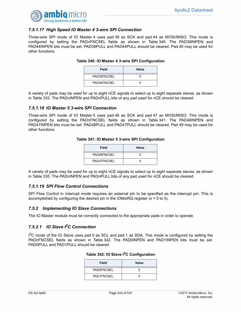
Apollo2 Datasheet
7.5.1.17 High Speed IO Master 4 3-wire SPI Connection
Three-wire SPI mode of IO Master 4 uses pad 39 as SCK and pad 44 as MOSI/MISO. This mode isconfigured by setting the PADnFNCSEL fields as shown in Table 340. The PAD39INPEN andPAD44INPEN bits must be set. PAD39PULL and PAD44PULL should be cleared. Pad 40 may be used forother functions.
A variety of pads may be used for up to eight nCE signals to select up to eight separate slaves, as shownin Table 333. The PADnINPEN and PADnPULL bits of any pad used for nCE should be cleared.
7.5.1.18 IO Master 5 3-wire SPI Connection
Three-wire SPI mode of IO Master 5 uses pad 48 as SCK and pad 47 as MOSI/MISO. This mode isconfigured by setting the PADnFNCSEL fields as shown in Table 341. The PAD48INPEN andPAD47INPEN bits must be set. PAD48PULL and PAD47PULL should be cleared. Pad 49 may be used forother functions.
A variety of pads may be used for up to eight nCE signals to select up to eight separate slaves, as shownin Table 335. The PADnINPEN and PADnPULL bits of any pad used for nCE should be cleared.
7.5.1.19 SPI Flow Control Connections
SPI Flow Control in interrupt mode requires an external pin to be specified as the interrupt pin. This isaccomplished by configuring the desired pin in the IOMxIRQ register (x = 0 to 5).
7.5.2 Implementing IO Slave Connections
The IO Master module must be correctly connected to the appropriate pads in order to operate.
7.5.2.1 IO Slave I2C Connection
I2C mode of the IO Slave uses pad 0 as SCL and pad 1 as SDA. This mode is configured by setting thePADnFNCSEL fields as shown in Table 342. The PAD0INPEN and PAD1INPEN bits must be set.PAD0PULL and PAD1PULL should be cleared.
Table 340: IO Master 4 3-wire SPI Configuration
Field Value
PAD39FNCSEL 5
PAD44FNCSEL 4
Table 341: IO Master 5 3-wire SPI Configuration
Field Value
PAD48FNCSEL 5
PAD47FNCSEL 4
Table 342: IO Slave I2C Configuration
Field Value
PAD0FNCSEL 0
PAD1FNCSEL 0
DS-A2-0p92 Page 233 of 537 2017 Ambiq Micro, Inc.All rights reserved.
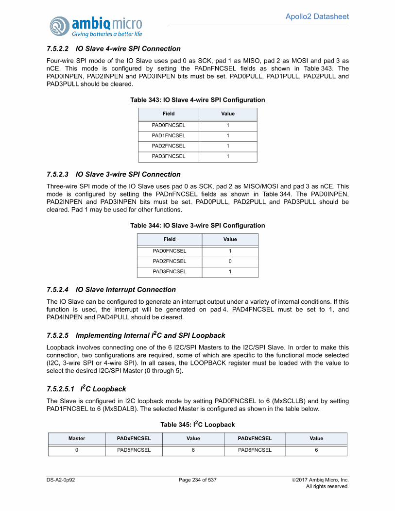
Apollo2 Datasheet
7.5.2.2 IO Slave 4-wire SPI Connection
Four-wire SPI mode of the IO Slave uses pad 0 as SCK, pad 1 as MISO, pad 2 as MOSI and pad 3 asnCE. This mode is configured by setting the PADnFNCSEL fields as shown in Table 343. ThePAD0INPEN, PAD2INPEN and PAD3INPEN bits must be set. PAD0PULL, PAD1PULL, PAD2PULL andPAD3PULL should be cleared.
7.5.2.3 IO Slave 3-wire SPI Connection
Three-wire SPI mode of the IO Slave uses pad 0 as SCK, pad 2 as MISO/MOSI and pad 3 as nCE. Thismode is configured by setting the PADnFNCSEL fields as shown in Table 344. The PAD0INPEN,PAD2INPEN and PAD3INPEN bits must be set. PAD0PULL, PAD2PULL and PAD3PULL should becleared. Pad 1 may be used for other functions.
7.5.2.4 IO Slave Interrupt Connection
The IO Slave can be configured to generate an interrupt output under a variety of internal conditions. If thisfunction is used, the interrupt will be generated on pad 4. PAD4FNCSEL must be set to 1, andPAD4INPEN and PAD4PULL should be cleared.
7.5.2.5 Implementing Internal I2C and SPI Loopback
Loopback involves connecting one of the 6 I2C/SPI Masters to the I2C/SPI Slave. In order to make thisconnection, two configurations are required, some of which are specific to the functional mode selected(I2C, 3-wire SPI or 4-wire SPI). In all cases, the LOOPBACK register must be loaded with the value toselect the desired I2C/SPI Master (0 through 5).
7.5.2.5.1 I2C Loopback
The Slave is configured in I2C loopback mode by setting PAD0FNCSEL to 6 (MxSCLLB) and by settingPAD1FNCSEL to 6 (MxSDALB). The selected Master is configured as shown in the table below.
Table 343: IO Slave 4-wire SPI Configuration
Field Value
PAD0FNCSEL 1
PAD1FNCSEL 1
PAD2FNCSEL 1
PAD3FNCSEL 1
Table 344: IO Slave 3-wire SPI Configuration
Field Value
PAD0FNCSEL 1
PAD2FNCSEL 0
PAD3FNCSEL 1
Table 345: I2C Loopback
Master PADxFNCSEL Value PADxFNCSEL Value
0 PAD5FNCSEL 6 PAD6FNCSEL 6
DS-A2-0p92 Page 234 of 537 2017 Ambiq Micro, Inc.All rights reserved.
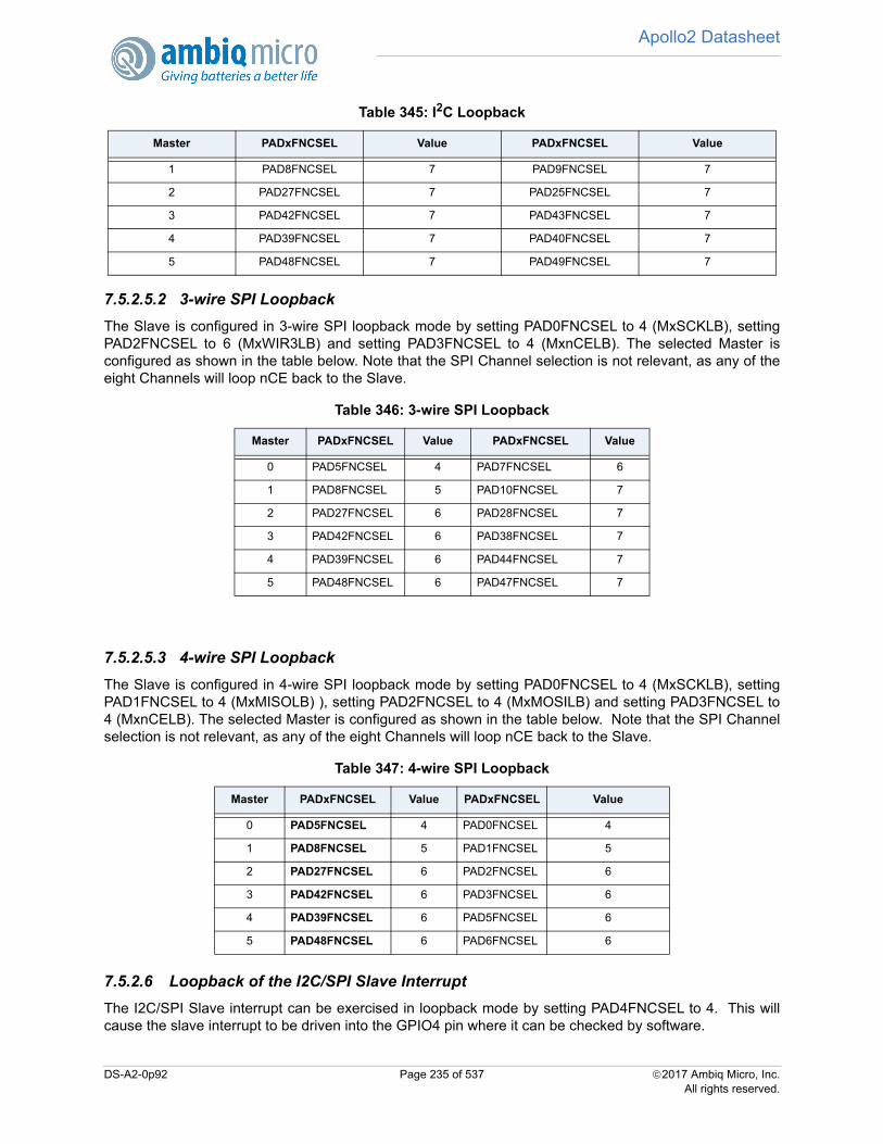
Apollo2 Datasheet
7.5.2.5.2 3-wire SPI Loopback
The Slave is configured in 3-wire SPI loopback mode by setting PAD0FNCSEL to 4 (MxSCKLB), settingPAD2FNCSEL to 6 (MxWIR3LB) and setting PAD3FNCSEL to 4 (MxnCELB). The selected Master isconfigured as shown in the table below. Note that the SPI Channel selection is not relevant, as any of theeight Channels will loop nCE back to the Slave.
7.5.2.5.3 4-wire SPI Loopback
The Slave is configured in 4-wire SPI loopback mode by setting PAD0FNCSEL to 4 (MxSCKLB), settingPAD1FNCSEL to 4 (MxMISOLB) ), setting PAD2FNCSEL to 4 (MxMOSILB) and setting PAD3FNCSEL to4 (MxnCELB). The selected Master is configured as shown in the table below. Note that the SPI Channelselection is not relevant, as any of the eight Channels will loop nCE back to the Slave.
7.5.2.6 Loopback of the I2C/SPI Slave Interrupt
The I2C/SPI Slave interrupt can be exercised in loopback mode by setting PAD4FNCSEL to 4. This willcause the slave interrupt to be driven into the GPIO4 pin where it can be checked by software.
1 PAD8FNCSEL 7 PAD9FNCSEL 7
2 PAD27FNCSEL 7 PAD25FNCSEL 7
3 PAD42FNCSEL 7 PAD43FNCSEL 7
4 PAD39FNCSEL 7 PAD40FNCSEL 7
5 PAD48FNCSEL 7 PAD49FNCSEL 7
Table 346: 3-wire SPI Loopback
Master PADxFNCSEL Value PADxFNCSEL Value
0 PAD5FNCSEL 4 PAD7FNCSEL 6
1 PAD8FNCSEL 5 PAD10FNCSEL 7
2 PAD27FNCSEL 6 PAD28FNCSEL 7
3 PAD42FNCSEL 6 PAD38FNCSEL 7
4 PAD39FNCSEL 6 PAD44FNCSEL 7
5 PAD48FNCSEL 6 PAD47FNCSEL 7
Table 347: 4-wire SPI Loopback
Master PADxFNCSEL Value PADxFNCSEL Value
0 PAD5FNCSEL 4 PAD0FNCSEL 4
1 PAD8FNCSEL 5 PAD1FNCSEL 5
2 PAD27FNCSEL 6 PAD2FNCSEL 6
3 PAD42FNCSEL 6 PAD3FNCSEL 6
4 PAD39FNCSEL 6 PAD5FNCSEL 6
5 PAD48FNCSEL 6 PAD6FNCSEL 6
Table 345: I2C Loopback
Master PADxFNCSEL Value PADxFNCSEL Value
DS-A2-0p92 Page 235 of 537 2017 Ambiq Micro, Inc.All rights reserved.
Apollo2 Datasheet
7.5.3 Implementing Counter/Timer Connections
Each Counter/Timer can optionally count pulses from an input pad, or generate pulses on an output pad.Table 348 shows the PADnFNCSEL settings to connect each Counter/Timer to the appropriate pad. If thepad is used as an input, the PADnINPEN bit should be set, otherwise it should be cleared. The PADnPULLbit may be set if the input signal is open drain.
DS-A2-0p92 Page 236 of 537 2017 Ambiq Micro, Inc.All rights reserved.
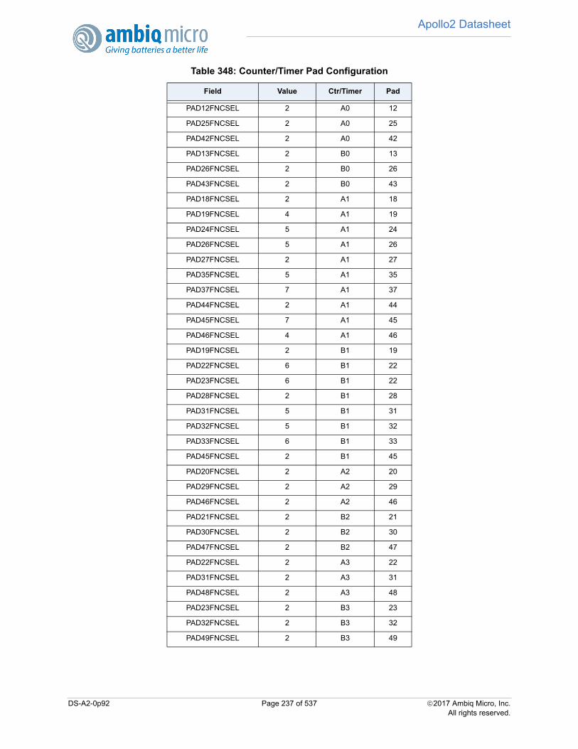
Apollo2 Datasheet
Table 348: Counter/Timer Pad Configuration
Field Value Ctr/Timer Pad
PAD12FNCSEL 2 A0 12
PAD25FNCSEL 2 A0 25
PAD42FNCSEL 2 A0 42
PAD13FNCSEL 2 B0 13
PAD26FNCSEL 2 B0 26
PAD43FNCSEL 2 B0 43
PAD18FNCSEL 2 A1 18
PAD19FNCSEL 4 A1 19
PAD24FNCSEL 5 A1 24
PAD26FNCSEL 5 A1 26
PAD27FNCSEL 2 A1 27
PAD35FNCSEL 5 A1 35
PAD37FNCSEL 7 A1 37
PAD44FNCSEL 2 A1 44
PAD45FNCSEL 7 A1 45
PAD46FNCSEL 4 A1 46
PAD19FNCSEL 2 B1 19
PAD22FNCSEL 6 B1 22
PAD23FNCSEL 6 B1 22
PAD28FNCSEL 2 B1 28
PAD31FNCSEL 5 B1 31
PAD32FNCSEL 5 B1 32
PAD33FNCSEL 6 B1 33
PAD45FNCSEL 2 B1 45
PAD20FNCSEL 2 A2 20
PAD29FNCSEL 2 A2 29
PAD46FNCSEL 2 A2 46
PAD21FNCSEL 2 B2 21
PAD30FNCSEL 2 B2 30
PAD47FNCSEL 2 B2 47
PAD22FNCSEL 2 A3 22
PAD31FNCSEL 2 A3 31
PAD48FNCSEL 2 A3 48
PAD23FNCSEL 2 B3 23
PAD32FNCSEL 2 B3 32
PAD49FNCSEL 2 B3 49
DS-A2-0p92 Page 237 of 537 2017 Ambiq Micro, Inc.All rights reserved.
Apollo2 Datasheet
7.5.4 Implementing UART Connections
The UART signals can be connected to a variety of pads.
7.5.4.1 UART0 TX/RX Connections
The UART data signals TX and RX may each be connected to several pads. Note that TX and RX areselected independently. Table 349 shows the connections for TX, which should have the correspondingPADnINPEN and PADnPULL bits clear. Table 350 shows the connections for RX, which must have thecorresponding PADnINPEN bit set and should have the corresponding PADnPULL bit clear.
DS-A2-0p92 Page 238 of 537 2017 Ambiq Micro, Inc.All rights reserved.

Apollo2 Datasheet
7.5.4.2 UART0 RTS/CTS Connections
The UART modem control signals RTS and CTS may each be connected to one of two pads. Note thatRTS and CTS are selected independently. Table 351 shows the connections for RTS, which should havethe corresponding PADnINPEN and PADnPULL bits clear. Table 352 shows the connections for CTS,which must have the corresponding PADnINPEN bit set and should have the corresponding PADnPULL bitclear.
Table 349: UART0 TX Configuration
Field Value Pad
PAD1FNCSEL 2 1
PAD7FNCSEL 5 7
PAD16FNCSEL 6 16
PAD20FNCSEL 4 20
PAD22FNCSEL 0 22
PAD30FNCSEL 4 30
PAD39FNCSEL 0 39
Table 350: UART0 RX Configuration
Field Value Pad
PAD2FNCSEL 2 2
PAD11FNCSEL 6 11
PAD17FNCSEL 6 17
PAD21FNCSEL 4 21
PAD23FNCSEL 0 23
PAD31FNCSEL 4 31
PAD40FNCSEL 0 40
Table 351: UART0 RTS Configuration
Field Value Pad
PAD3FNCSEL 0 3
PAD5FNCSEL 2 5
PAD13FNCSEL 6 13
PAD35FNCSEL 6 35
PAD37FNCSEL 2 37
PAD41FNCSEL 7 41
DS-A2-0p92 Page 239 of 537 2017 Ambiq Micro, Inc.All rights reserved.

Apollo2 Datasheet
7.5.4.3 UART1 TX/RX Connections
The UART data signals TX and RX may each be connected to several pads. Note that TX and RX areselected independently. Table 349 shows the connections for TX, which should have the correspondingPADnINPEN and PADnPULL bits clear. Table 350 shows the connections for RX, which must have thecorresponding PADnINPEN bit set and should have the corresponding PADnPULL bit clear.
Table 352: UART0 CTS Configuration
Field Value Pad
PAD4FNCSEL 0 4
PAD6FNCSEL 2 6
PAD12FNCSEL 6 12
PAD29FNCSEL 4 29
PAD36FNCSEL 6 36
PAD38FNCSEL 2 38
DS-A2-0p92 Page 240 of 537 2017 Ambiq Micro, Inc.All rights reserved.

Apollo2 Datasheet
7.5.4.4 UART1 RTS/CTS Connections
The UART modem control signals RTS and CTS may each be connected to one of two pads. Note thatRTS and CTS are selected independently. Table 351 shows the connections for RTS, which should havethe corresponding PADnINPEN and PADnPULL bits clear. Table 352 shows the connections for CTS,which must have the corresponding PADnINPEN bit set and should have the corresponding PADnPULL bitclear.
Table 353: UART1 TX Configuration
Field Value Pad
PAD8FNCSEL 6 8
PAD12FNCSEL 7 12
PAD14FNCSEL 2 14
PAD18FNCSEL 6 18
PAD20FNCSEL 5 20
PAD35FNCSEL 2 35
PAD39FNCSEL 1 39
Table 354: UART1 RX Configuration
Field Value Pad
PAD9FNCSEL 6 9
PAD13FNCSEL 7 13
PAD15FNCSEL 2 15
PAD19FNCSEL 6 19
PAD21FNCSEL 5 21
PAD36FNCSEL 2 36
PAD40FNCSEL 1 40
Table 355: UART1 RTS Configuration
Field Value Pad
PAD10FNCSEL 5 10
PAD16FNCSEL 7 16
PAD30FNCSEL 5 30
PAD44FNCSEL 0 44
Table 356: UART1 CTS Configuration
Field Value Pad
PAD11FNCSEL 5 11
PAD17FNCSEL 7 17
PAD29FNCSEL 5 29
PAD45FNCSEL 0 45
DS-A2-0p92 Page 241 of 537 2017 Ambiq Micro, Inc.All rights reserved.
Apollo2 Datasheet
7.5.5 Implementing Audio Connections
The Audio signals can be connected to a variety of pads.
7.5.5.1 PDM Connections
The PDM CLK and DATA signals may each be connected to several pads. Note that CLK and DATA areselected independently. Table 357 shows the connections for PDM CLK, which should have thecorresponding PADnINPEN and PADnPULL bits clear. Table 358 shows the connections for PDM DATA,which must have the corresponding PADnINPEN bit set and should have the corresponding PADnPULL bitclear.
DS-A2-0p92 Page 242 of 537 2017 Ambiq Micro, Inc.All rights reserved.

Apollo2 Datasheet
7.5.5.2 I2S Connections
The I2S BCLK, WCLK and DAT signals may each be connected to several pads. Note that BCLK, WCLKand DAT are selected independently. Table 359 shows the connections for PDM BCLK, which should havethe corresponding PADnINPEN and PADnPULL bits clear. Table 359 shows the connections for PDMWCLK, which should have the corresponding PADnINPEN and PADnPULL bits clear. Table 361 shows theconnections for PDM DAT, which must have the corresponding PADnINPEN bit set and should have thecorresponding PADnPULL bit clear.
Table 357: PDM CLK Configuration
Field Value Pad
PAD12FNCSEL 5 12
PAD22FNCSEL 4 22
PAD37FNCSEL 6 37
Table 358: PDM DATA Configuration
Field Value Pad
PAD11FNCSEL 7 11
PAD23FNCSEL 4 23
PAD29FNCSEL 7 31
Table 359: I2S BCLK Configuration
Field Value Pad
PAD19FNCSEL 7 19
PAD24FNCSEL 6 24
Table 360: I2S WCLK Configuration
Field Value Pad
PAD3FNCSEL 7 3
PAD28FNCSEL 0 28
Table 361: I2S DAT Configuration
Field Value Pad
PAD6FNCSEL 7 6
PAD30FNCSEL 7 30
DS-A2-0p92 Page 243 of 537 2017 Ambiq Micro, Inc.All rights reserved.

Apollo2 Datasheet
7.5.6 Implementing GPIO Connections
Each pad of the Apollo2 MCU can be configured as a GPIO port by setting PADnFNCSEL to 3.PADnINPEN and PADnPULL must be set appropriately depending on the specific GPIO function.
7.5.7 Implementing CLKOUT Connections
The flexible clock output of the Clock Generator module, CLKOUT, may be configured on several pads asshown in Table 362. PADnINPEN and PADnPULL should be cleared in each case.
7.5.8 Implementing 32kHz CLKOUT Connections
In addition to the CLKOUT mux output, there is also a dedicated 32 kHz clock output. This clock isprimarily for leveraging the 32 kHz oscillator clock from Apollo2 MCU . This clock output may beconfigured on several pads as shown in Table 363. PADnINPEN and PADnPULL should be cleared ineach case.
7.5.9 Implementing ADC Connections
Three types of pad connections may be made for the ADC module. Up to ten pads may be configured asthe analog inputs, as shown in Table 364. The ADCREF reference voltage input is supplied on a dedicatedinput pin. If an external digital trigger is desired, up to four selectable pad choices may be configured, as
Table 362: CLKOUT Configuration
Field Value Pad
PAD0FNCSEL 2 0
PAD4FNCSEL 6 4
PAD7FNCSEL 2 7
PAD11FNCSEL 2 11
PAD12FNCSEL 4 12
PAD24FNCSEL 2 24
PAD39FNCSEL 2 39
PAD41FNCSEL 1 41
Table 363: 32kHz CLKOUT Configuration
Field Value Pad
PAD4FNCSEL 7 4
PAD14FNCSEL 7 14
PAD18FNCSEL 7 18
PAD33FNCSEL 2 33
PAD36FNCSEL 4 36
PAD46FNCSEL 0 46
DS-A2-0p92 Page 244 of 537 2017 Ambiq Micro, Inc.All rights reserved.
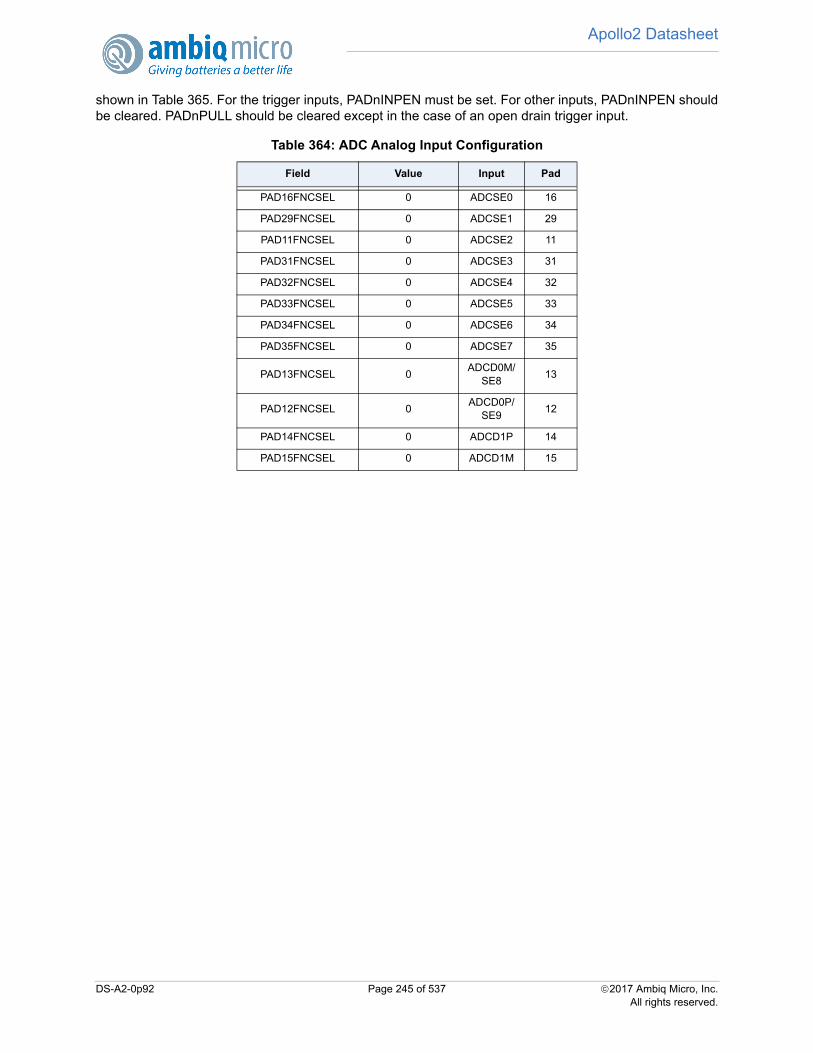
Apollo2 Datasheet
shown in Table 365. For the trigger inputs, PADnINPEN must be set. For other inputs, PADnINPEN shouldbe cleared. PADnPULL should be cleared except in the case of an open drain trigger input.
Table 364: ADC Analog Input Configuration
Field Value Input Pad
PAD16FNCSEL 0 ADCSE0 16
PAD29FNCSEL 0 ADCSE1 29
PAD11FNCSEL 0 ADCSE2 11
PAD31FNCSEL 0 ADCSE3 31
PAD32FNCSEL 0 ADCSE4 32
PAD33FNCSEL 0 ADCSE5 33
PAD34FNCSEL 0 ADCSE6 34
PAD35FNCSEL 0 ADCSE7 35
PAD13FNCSEL 0ADCD0M/
SE813
PAD12FNCSEL 0ADCD0P/
SE912
PAD14FNCSEL 0 ADCD1P 14
PAD15FNCSEL 0 ADCD1M 15
DS-A2-0p92 Page 245 of 537 2017 Ambiq Micro, Inc.All rights reserved.
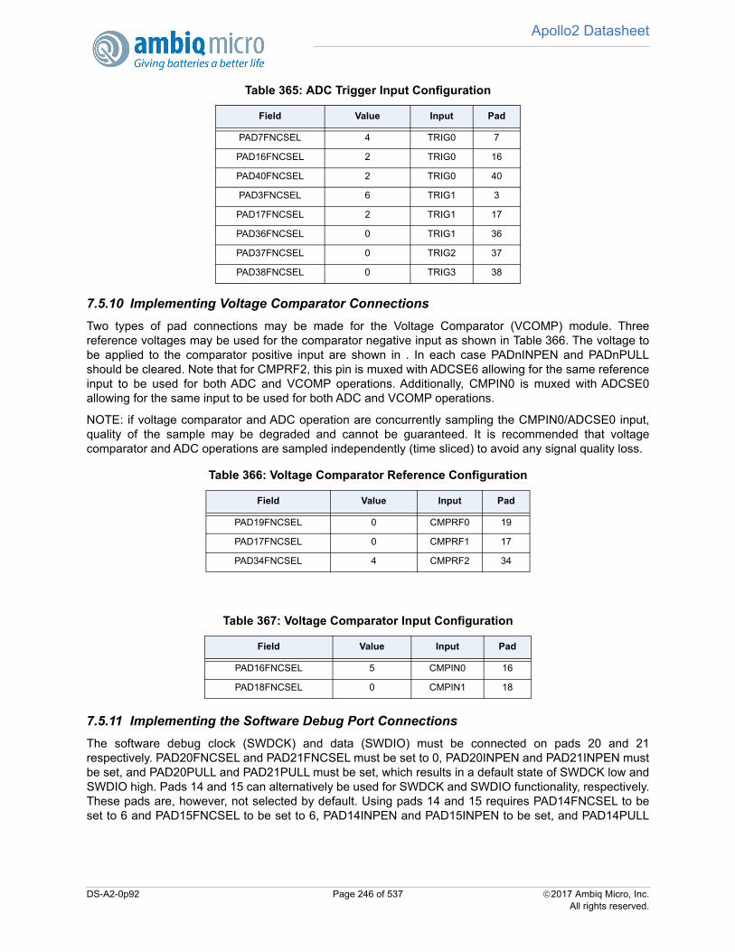
Apollo2 Datasheet
7.5.10 Implementing Voltage Comparator Connections
Two types of pad connections may be made for the Voltage Comparator (VCOMP) module. Threereference voltages may be used for the comparator negative input as shown in Table 366. The voltage tobe applied to the comparator positive input are shown in . In each case PADnINPEN and PADnPULLshould be cleared. Note that for CMPRF2, this pin is muxed with ADCSE6 allowing for the same referenceinput to be used for both ADC and VCOMP operations. Additionally, CMPIN0 is muxed with ADCSE0allowing for the same input to be used for both ADC and VCOMP operations.
NOTE: if voltage comparator and ADC operation are concurrently sampling the CMPIN0/ADCSE0 input,quality of the sample may be degraded and cannot be guaranteed. It is recommended that voltagecomparator and ADC operations are sampled independently (time sliced) to avoid any signal quality loss.
7.5.11 Implementing the Software Debug Port Connections
The software debug clock (SWDCK) and data (SWDIO) must be connected on pads 20 and 21respectively. PAD20FNCSEL and PAD21FNCSEL must be set to 0, PAD20INPEN and PAD21INPEN mustbe set, and PAD20PULL and PAD21PULL must be set, which results in a default state of SWDCK low andSWDIO high. Pads 14 and 15 can alternatively be used for SWDCK and SWDIO functionality, respectively.These pads are, however, not selected by default. Using pads 14 and 15 requires PAD14FNCSEL to beset to 6 and PAD15FNCSEL to be set to 6, PAD14INPEN and PAD15INPEN to be set, and PAD14PULL
Table 365: ADC Trigger Input Configuration
Field Value Input Pad
PAD7FNCSEL 4 TRIG0 7
PAD16FNCSEL 2 TRIG0 16
PAD40FNCSEL 2 TRIG0 40
PAD3FNCSEL 6 TRIG1 3
PAD17FNCSEL 2 TRIG1 17
PAD36FNCSEL 0 TRIG1 36
PAD37FNCSEL 0 TRIG2 37
PAD38FNCSEL 0 TRIG3 38
Table 366: Voltage Comparator Reference Configuration
Field Value Input Pad
PAD19FNCSEL 0 CMPRF0 19
PAD17FNCSEL 0 CMPRF1 17
PAD34FNCSEL 4 CMPRF2 34
Table 367: Voltage Comparator Input Configuration
Field Value Input Pad
PAD16FNCSEL 5 CMPIN0 16
PAD18FNCSEL 0 CMPIN1 18
DS-A2-0p92 Page 246 of 537 2017 Ambiq Micro, Inc.All rights reserved.
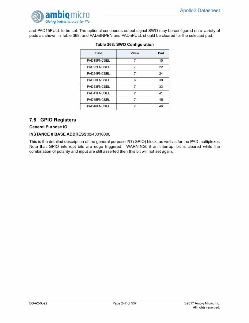
Apollo2 Datasheet
and PAD15PULL to be set. The optional continuous output signal SWO may be configured on a variety ofpads as shown in Table 368, and PADnINPEN and PADnPULL should be cleared for the selected pad.
7.6 GPIO RegistersGeneral Purpose IO
INSTANCE 0 BASE ADDRESS:0x40010000
This is the detailed description of the general purpose I/O (GPIO) block, as well as for the PAD multiplexor.Note that GPIO interrupt bits are edge triggered. WARNING: if an interrupt bit is cleared while thecombination of polarity and input are still asserted then this bit will not set again.
Table 368: SWO Configuration
Field Value Pad
PAD15FNCSEL 7 15
PAD22FNCSEL 7 22
PAD24FNCSEL 7 24
PAD30FNCSEL 6 30
PAD33FNCSEL 7 33
PAD41FNCSEL 2 41
PAD45FNCSEL 7 45
PAD46FNCSEL 7 46
DS-A2-0p92 Page 247 of 537 2017 Ambiq Micro, Inc.All rights reserved.
Apollo2 Datasheet
7.6.1 Register Memory Map
Table 369: GPIO Register Map
Address(s) Register Name Description
0x40010000 PADREGA Pad Configuration Register A
0x40010004 PADREGB Pad Configuration Register B
0x40010008 PADREGC Pad Configuration Register C
0x4001000C PADREGD Pad Configuration Register D
0x40010010 PADREGE Pad Configuration Register E
0x40010014 PADREGF Pad Configuration Register F
0x40010018 PADREGG Pad Configuration Register G
0x4001001C PADREGH Pad Configuration Register H
0x40010020 PADREGI Pad Configuration Register I
0x40010024 PADREGJ Pad Configuration Register J
0x40010028 PADREGK Pad Configuration Register K
0x4001002C PADREGL Pad Configuration Register L
0x40010030 PADREGM Pad Configuration Register M
0x40010040 CFGA GPIO Configuration Register A
0x40010044 CFGB GPIO Configuration Register B
0x40010048 CFGC GPIO Configuration Register C
0x4001004C CFGD GPIO Configuration Register D
0x40010050 CFGE GPIO Configuration Register E
0x40010054 CFGF GPIO Configuration Register F
0x40010058 CFGG GPIO Configuration Register G
0x40010060 PADKEY Key Register for all pad configuration registers
0x40010080 RDA GPIO Input Register A
0x40010084 RDB GPIO Input Register B
0x40010088 WTA GPIO Output Register A
0x4001008C WTB GPIO Output Register B
0x40010090 WTSA GPIO Output Register A Set
0x40010094 WTSB GPIO Output Register B Set
0x40010098 WTCA GPIO Output Register A Clear
0x4001009C WTCB GPIO Output Register B Clear
0x400100A0 ENA GPIO Enable Register A
0x400100A4 ENB GPIO Enable Register B
0x400100A8 ENSA GPIO Enable Register A Set
0x400100AC ENSB GPIO Enable Register B Set
0x400100B4 ENCA GPIO Enable Register A Clear
0x400100B8 ENCB GPIO Enable Register B Clear
0x400100BC STMRCAP STIMER Capture Control
DS-A2-0p92 Page 248 of 537 2017 Ambiq Micro, Inc.All rights reserved.
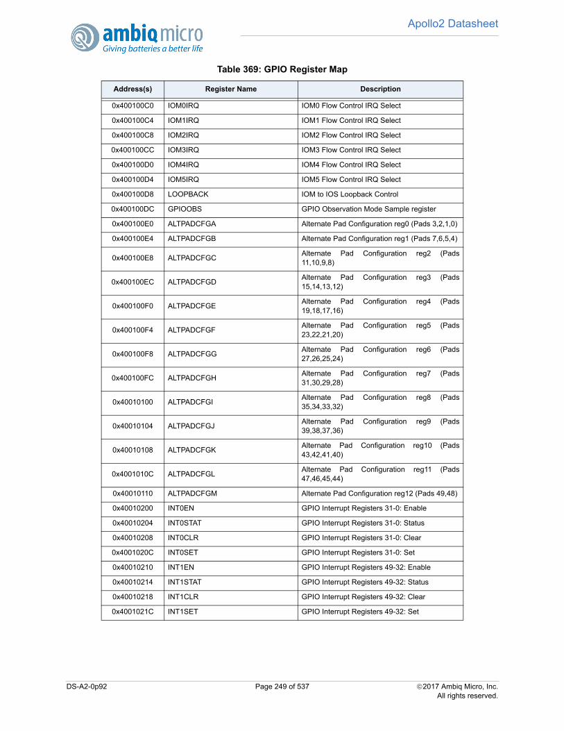
Apollo2 Datasheet
0x400100C0 IOM0IRQ IOM0 Flow Control IRQ Select
0x400100C4 IOM1IRQ IOM1 Flow Control IRQ Select
0x400100C8 IOM2IRQ IOM2 Flow Control IRQ Select
0x400100CC IOM3IRQ IOM3 Flow Control IRQ Select
0x400100D0 IOM4IRQ IOM4 Flow Control IRQ Select
0x400100D4 IOM5IRQ IOM5 Flow Control IRQ Select
0x400100D8 LOOPBACK IOM to IOS Loopback Control
0x400100DC GPIOOBS GPIO Observation Mode Sample register
0x400100E0 ALTPADCFGA Alternate Pad Configuration reg0 (Pads 3,2,1,0)
0x400100E4 ALTPADCFGB Alternate Pad Configuration reg1 (Pads 7,6,5,4)
0x400100E8 ALTPADCFGCAlternate Pad Configuration reg2 (Pads11,10,9,8)
0x400100EC ALTPADCFGDAlternate Pad Configuration reg3 (Pads15,14,13,12)
0x400100F0 ALTPADCFGEAlternate Pad Configuration reg4 (Pads19,18,17,16)
0x400100F4 ALTPADCFGFAlternate Pad Configuration reg5 (Pads23,22,21,20)
0x400100F8 ALTPADCFGGAlternate Pad Configuration reg6 (Pads27,26,25,24)
0x400100FC ALTPADCFGHAlternate Pad Configuration reg7 (Pads31,30,29,28)
0x40010100 ALTPADCFGIAlternate Pad Configuration reg8 (Pads35,34,33,32)
0x40010104 ALTPADCFGJAlternate Pad Configuration reg9 (Pads39,38,37,36)
0x40010108 ALTPADCFGKAlternate Pad Configuration reg10 (Pads43,42,41,40)
0x4001010C ALTPADCFGLAlternate Pad Configuration reg11 (Pads47,46,45,44)
0x40010110 ALTPADCFGM Alternate Pad Configuration reg12 (Pads 49,48)
0x40010200 INT0EN GPIO Interrupt Registers 31-0: Enable
0x40010204 INT0STAT GPIO Interrupt Registers 31-0: Status
0x40010208 INT0CLR GPIO Interrupt Registers 31-0: Clear
0x4001020C INT0SET GPIO Interrupt Registers 31-0: Set
0x40010210 INT1EN GPIO Interrupt Registers 49-32: Enable
0x40010214 INT1STAT GPIO Interrupt Registers 49-32: Status
0x40010218 INT1CLR GPIO Interrupt Registers 49-32: Clear
0x4001021C INT1SET GPIO Interrupt Registers 49-32: Set
Table 369: GPIO Register Map
Address(s) Register Name Description
DS-A2-0p92 Page 249 of 537 2017 Ambiq Micro, Inc.All rights reserved.
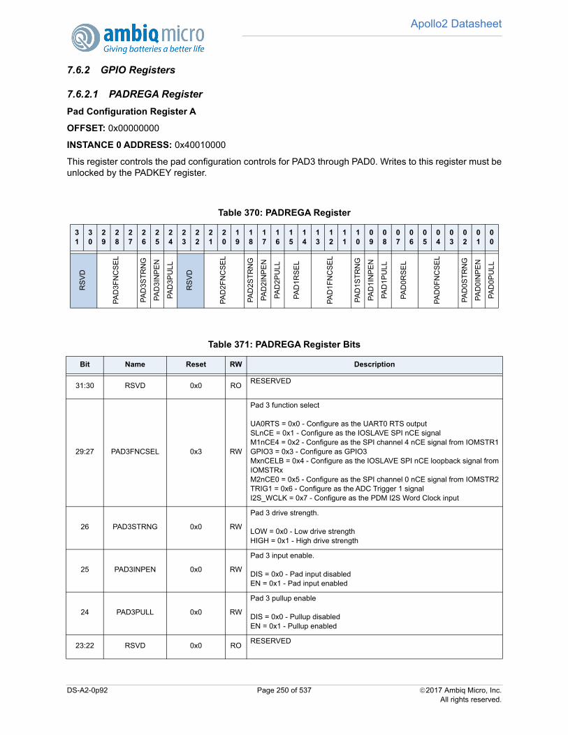
Apollo2 Datasheet
7.6.2 GPIO Registers
7.6.2.1 PADREGA Register
Pad Configuration Register A
OFFSET: 0x00000000
INSTANCE 0 ADDRESS: 0x40010000
This register controls the pad configuration controls for PAD3 through PAD0. Writes to this register must beunlocked by the PADKEY register.
Table 370: PADREGA Register
31
30
29
28
27
26
25
24
23
22
21
20
19
18
17
16
15
14
13
12
11
10
09
08
07
06
05
04
03
02
01
00
RS
VD
PA
D3F
NC
SE
L
PA
D3S
TR
NG
PA
D3I
NP
EN
PA
D3P
ULL
RS
VD
PA
D2F
NC
SE
L
PA
D2S
TR
NG
PA
D2I
NP
EN
PA
D2P
ULL
PA
D1
RS
EL
PA
D1F
NC
SE
L
PA
D1S
TR
NG
PA
D1I
NP
EN
PA
D1P
ULL
PA
D0
RS
EL
PA
D0F
NC
SE
L
PA
D0S
TR
NG
PA
D0I
NP
EN
PA
D0P
ULL
Table 371: PADREGA Register Bits
Bit Name Reset RW Description
31:30 RSVD 0x0 RORESERVED
29:27 PAD3FNCSEL 0x3 RW
Pad 3 function select
UA0RTS = 0x0 - Configure as the UART0 RTS outputSLnCE = 0x1 - Configure as the IOSLAVE SPI nCE signalM1nCE4 = 0x2 - Configure as the SPI channel 4 nCE signal from IOMSTR1GPIO3 = 0x3 - Configure as GPIO3MxnCELB = 0x4 - Configure as the IOSLAVE SPI nCE loopback signal fromIOMSTRxM2nCE0 = 0x5 - Configure as the SPI channel 0 nCE signal from IOMSTR2TRIG1 = 0x6 - Configure as the ADC Trigger 1 signalI2S_WCLK = 0x7 - Configure as the PDM I2S Word Clock input
26 PAD3STRNG 0x0 RW
Pad 3 drive strength.
LOW = 0x0 - Low drive strengthHIGH = 0x1 - High drive strength
25 PAD3INPEN 0x0 RW
Pad 3 input enable.
DIS = 0x0 - Pad input disabledEN = 0x1 - Pad input enabled
24 PAD3PULL 0x0 RW
Pad 3 pullup enable
DIS = 0x0 - Pullup disabledEN = 0x1 - Pullup enabled
23:22 RSVD 0x0 RORESERVED
DS-A2-0p92 Page 250 of 537 2017 Ambiq Micro, Inc.All rights reserved.
Apollo2 Datasheet
21:19 PAD2FNCSEL 0x3 RW
Pad 2 function select
SLWIR3 = 0x0 - Configure as the IOSLAVE SPI 3-wire MOSI/MISO signalSLMOSI = 0x1 - Configure as the IOSLAVE SPI MOSI signalUART0RX = 0x2 - Configure as the UART0 RX inputGPIO2 = 0x3 - Configure as GPIO2MxMOSILB = 0x4 - Configure as the IOSLAVE SPI MOSI loopback signalfrom IOMSTRxM2MOSI = 0x5 - Configure as the IOMSTR2 SPI MOSI output signalMxWIR3LB = 0x6 - Configure as the IOSLAVE SPI 3-wire MOSI/MISO loop-back signal from IOMSTRxM2WIR3 = 0x7 - Configure as the IOMSTR2 SPI 3-wire MOSI/MISO signal
18 PAD2STRNG 0x0 RW
Pad 2 drive strength
LOW = 0x0 - Low drive strengthHIGH = 0x1 - High drive strength
17 PAD2INPEN 0x0 RW
Pad 2 input enable
DIS = 0x0 - Pad input disabledEN = 0x1 - Pad input enabled
16 PAD2PULL 0x0 RW
Pad 2 pullup enable
DIS = 0x0 - Pullup disabledEN = 0x1 - Pullup enabled
15:14 PAD1RSEL 0x0 RW
Pad 1 pullup resistor selection.
PULL1_5K = 0x0 - Pullup is ~1.5 KOhmsPULL6K = 0x1 - Pullup is ~6 KOhmsPULL12K = 0x2 - Pullup is ~12 KOhmsPULL24K = 0x3 - Pullup is ~24 KOhms
13:11 PAD1FNCSEL 0x3 RW
Pad 1 function select
SLSDA = 0x0 - Configure as the IOSLAVE I2C SDA signalSLMISO = 0x1 - Configure as the IOSLAVE SPI MISO signalUART0TX = 0x2 - Configure as the UART0 TX output signalGPIO1 = 0x3 - Configure as GPIO1MxMISOLB = 0x4 - Configure as the IOSLAVE SPI MISO loopback signalfrom IOMSTRxM2MISO = 0x5 - Configure as the IOMSTR2 SPI MISO input signalMxSDALB = 0x6 - Configure as the IOSLAVE I2C SDA loopback signal fromIOMSTRxM2SDA = 0x7 - Configure as the IOMSTR2 I2C Serial data I/O signal
10 PAD1STRNG 0x0 RW
Pad 1 drive strength
LOW = 0x0 - Low drive strengthHIGH = 0x1 - High drive strength
9 PAD1INPEN 0x0 RW
Pad 1 input enable
DIS = 0x0 - Pad input disabledEN = 0x1 - Pad input enabled
8 PAD1PULL 0x0 RW
Pad 1 pullup enable
DIS = 0x0 - Pullup disabledEN = 0x1 - Pullup enabled
Table 371: PADREGA Register Bits
Bit Name Reset RW Description
DS-A2-0p92 Page 251 of 537 2017 Ambiq Micro, Inc.All rights reserved.
Apollo2 Datasheet
7.6.2.2 PADREGB Register
Pad Configuration Register B
OFFSET: 0x00000004
INSTANCE 0 ADDRESS: 0x40010004
This register controls the pad configuration controls for PAD7 through PAD4. Writes to this register must beunlocked by the PADKEY register.
7:6 PAD0RSEL 0x0 RW
Pad 0 pullup resistor selection.
PULL1_5K = 0x0 - Pullup is ~1.5 KOhmsPULL6K = 0x1 - Pullup is ~6 KOhmsPULL12K = 0x2 - Pullup is ~12 KOhmsPULL24K = 0x3 - Pullup is ~24 KOhms
5:3 PAD0FNCSEL 0x3 RW
Pad 0 function select
SLSCL = 0x0 - Configure as the IOSLAVE I2C SCL signalSLSCK = 0x1 - Configure as the IOSLAVE SPI SCK signalCLKOUT = 0x2 - Configure as the CLKOUT signalGPIO0 = 0x3 - Configure as GPIO0MxSCKLB = 0x4 - Configure as the IOSLAVE SPI SCK loopback signal fromIOMSTRxM2SCK = 0x5 - Configure as the IOMSTR2 SPI SCK outputMxSCLLB = 0x6 - Configure as the IOSLAVE I2C SCL loopback signal fromIOMSTRxM2SCL = 0x7 - Configure as the IOMSTR2 I2C SCL clock I/O signal
2 PAD0STRNG 0x0 RW
Pad 0 drive strength
LOW = 0x0 - Low drive strengthHIGH = 0x1 - High drive strength
1 PAD0INPEN 0x0 RW
Pad 0 input enable
DIS = 0x0 - Pad input disabledEN = 0x1 - Pad input enabled
0 PAD0PULL 0x0 RW
Pad 0 pullup enable
DIS = 0x0 - Pullup disabledEN = 0x1 - Pullup enabled
Table 372: PADREGB Register
31
30
29
28
27
26
25
24
23
22
21
20
19
18
17
16
15
14
13
12
11
10
09
08
07
06
05
04
03
02
01
00
RS
VD
PA
D7F
NC
SE
L
PA
D7S
TR
NG
PA
D7I
NP
EN
PA
D7P
ULL
PA
D6R
SE
L
PA
D6F
NC
SE
L
PA
D6S
TR
NG
PA
D6I
NP
EN
PA
D6P
ULL
PA
D5R
SE
L
PA
D5F
NC
SE
L
PA
D5S
TR
NG
PA
D5I
NP
EN
PA
D5P
ULL
PA
D4P
WR
DN
RS
VD
PA
D4F
NC
SE
L
PA
D4S
TR
NG
PA
D4I
NP
EN
PA
D4P
ULL
Table 371: PADREGA Register Bits
Bit Name Reset RW Description
DS-A2-0p92 Page 252 of 537 2017 Ambiq Micro, Inc.All rights reserved.
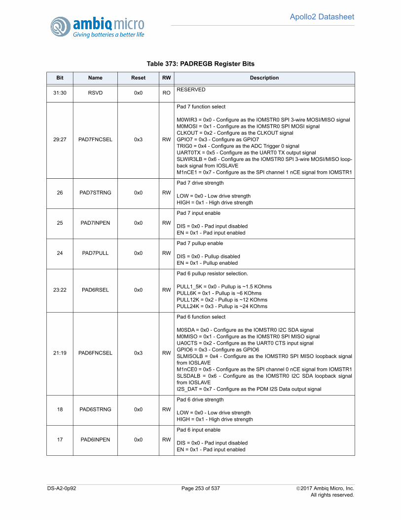
Apollo2 Datasheet
Table 373: PADREGB Register Bits
Bit Name Reset RW Description
31:30 RSVD 0x0 RORESERVED
29:27 PAD7FNCSEL 0x3 RW
Pad 7 function select
M0WIR3 = 0x0 - Configure as the IOMSTR0 SPI 3-wire MOSI/MISO signalM0MOSI = 0x1 - Configure as the IOMSTR0 SPI MOSI signalCLKOUT = 0x2 - Configure as the CLKOUT signalGPIO7 = 0x3 - Configure as GPIO7TRIG0 = 0x4 - Configure as the ADC Trigger 0 signalUART0TX = 0x5 - Configure as the UART0 TX output signalSLWIR3LB = 0x6 - Configure as the IOMSTR0 SPI 3-wire MOSI/MISO loop-back signal from IOSLAVEM1nCE1 = 0x7 - Configure as the SPI channel 1 nCE signal from IOMSTR1
26 PAD7STRNG 0x0 RW
Pad 7 drive strength
LOW = 0x0 - Low drive strengthHIGH = 0x1 - High drive strength
25 PAD7INPEN 0x0 RW
Pad 7 input enable
DIS = 0x0 - Pad input disabledEN = 0x1 - Pad input enabled
24 PAD7PULL 0x0 RW
Pad 7 pullup enable
DIS = 0x0 - Pullup disabledEN = 0x1 - Pullup enabled
23:22 PAD6RSEL 0x0 RW
Pad 6 pullup resistor selection.
PULL1_5K = 0x0 - Pullup is ~1.5 KOhmsPULL6K = 0x1 - Pullup is ~6 KOhmsPULL12K = 0x2 - Pullup is ~12 KOhmsPULL24K = 0x3 - Pullup is ~24 KOhms
21:19 PAD6FNCSEL 0x3 RW
Pad 6 function select
M0SDA = 0x0 - Configure as the IOMSTR0 I2C SDA signalM0MISO = 0x1 - Configure as the IOMSTR0 SPI MISO signalUA0CTS = 0x2 - Configure as the UART0 CTS input signalGPIO6 = 0x3 - Configure as GPIO6SLMISOLB = 0x4 - Configure as the IOMSTR0 SPI MISO loopback signalfrom IOSLAVEM1nCE0 = 0x5 - Configure as the SPI channel 0 nCE signal from IOMSTR1SLSDALB = 0x6 - Configure as the IOMSTR0 I2C SDA loopback signalfrom IOSLAVEI2S_DAT = 0x7 - Configure as the PDM I2S Data output signal
18 PAD6STRNG 0x0 RW
Pad 6 drive strength
LOW = 0x0 - Low drive strengthHIGH = 0x1 - High drive strength
17 PAD6INPEN 0x0 RW
Pad 6 input enable
DIS = 0x0 - Pad input disabledEN = 0x1 - Pad input enabled
DS-A2-0p92 Page 253 of 537 2017 Ambiq Micro, Inc.All rights reserved.
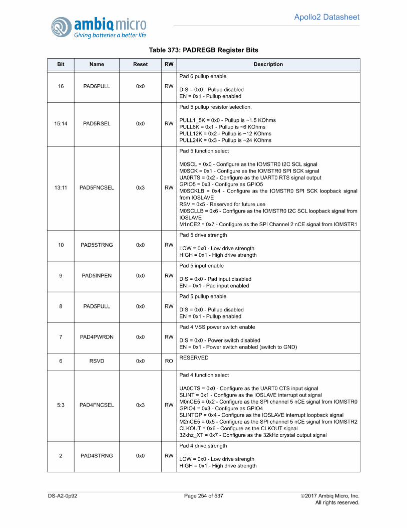
Apollo2 Datasheet
16 PAD6PULL 0x0 RW
Pad 6 pullup enable
DIS = 0x0 - Pullup disabledEN = 0x1 - Pullup enabled
15:14 PAD5RSEL 0x0 RW
Pad 5 pullup resistor selection.
PULL1_5K = 0x0 - Pullup is ~1.5 KOhmsPULL6K = 0x1 - Pullup is ~6 KOhmsPULL12K = 0x2 - Pullup is ~12 KOhmsPULL24K = 0x3 - Pullup is ~24 KOhms
13:11 PAD5FNCSEL 0x3 RW
Pad 5 function select
M0SCL = 0x0 - Configure as the IOMSTR0 I2C SCL signalM0SCK = 0x1 - Configure as the IOMSTR0 SPI SCK signalUA0RTS = 0x2 - Configure as the UART0 RTS signal outputGPIO5 = 0x3 - Configure as GPIO5M0SCKLB = 0x4 - Configure as the IOMSTR0 SPI SCK loopback signalfrom IOSLAVERSV = 0x5 - Reserved for future useM0SCLLB = 0x6 - Configure as the IOMSTR0 I2C SCL loopback signal fromIOSLAVEM1nCE2 = 0x7 - Configure as the SPI Channel 2 nCE signal from IOMSTR1
10 PAD5STRNG 0x0 RW
Pad 5 drive strength
LOW = 0x0 - Low drive strengthHIGH = 0x1 - High drive strength
9 PAD5INPEN 0x0 RW
Pad 5 input enable
DIS = 0x0 - Pad input disabledEN = 0x1 - Pad input enabled
8 PAD5PULL 0x0 RW
Pad 5 pullup enable
DIS = 0x0 - Pullup disabledEN = 0x1 - Pullup enabled
7 PAD4PWRDN 0x0 RW
Pad 4 VSS power switch enable
DIS = 0x0 - Power switch disabledEN = 0x1 - Power switch enabled (switch to GND)
6 RSVD 0x0 RORESERVED
5:3 PAD4FNCSEL 0x3 RW
Pad 4 function select
UA0CTS = 0x0 - Configure as the UART0 CTS input signalSLINT = 0x1 - Configure as the IOSLAVE interrupt out signalM0nCE5 = 0x2 - Configure as the SPI channel 5 nCE signal from IOMSTR0GPIO4 = 0x3 - Configure as GPIO4SLINTGP = 0x4 - Configure as the IOSLAVE interrupt loopback signalM2nCE5 = 0x5 - Configure as the SPI channel 5 nCE signal from IOMSTR2CLKOUT = 0x6 - Configure as the CLKOUT signal32khz_XT = 0x7 - Configure as the 32kHz crystal output signal
2 PAD4STRNG 0x0 RW
Pad 4 drive strength
LOW = 0x0 - Low drive strengthHIGH = 0x1 - High drive strength
Table 373: PADREGB Register Bits
Bit Name Reset RW Description
DS-A2-0p92 Page 254 of 537 2017 Ambiq Micro, Inc.All rights reserved.
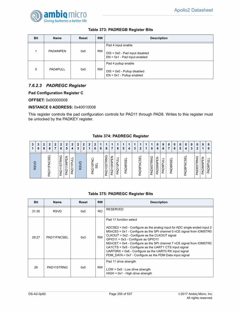
Apollo2 Datasheet
7.6.2.3 PADREGC Register
Pad Configuration Register C
OFFSET: 0x00000008
INSTANCE 0 ADDRESS: 0x40010008
This register controls the pad configuration controls for PAD11 through PAD8. Writes to this register mustbe unlocked by the PADKEY register.
1 PAD4INPEN 0x0 RW
Pad 4 input enable
DIS = 0x0 - Pad input disabledEN = 0x1 - Pad input enabled
0 PAD4PULL 0x0 RW
Pad 4 pullup enable
DIS = 0x0 - Pullup disabledEN = 0x1 - Pullup enabled
Table 374: PADREGC Register
31
30
29
28
27
26
25
24
23
22
21
20
19
18
17
16
15
14
13
12
11
10
09
08
07
06
05
04
03
02
01
00
RS
VD
PA
D11
FN
CS
EL
PA
D11
ST
RN
G
PA
D11
INP
EN
PA
D11
PU
LL
RS
VD
PA
D10
FN
C-
SE
L
PA
D1
0ST
RN
G
PA
D10
INP
EN
PA
D10
PU
LL
PA
D9
RS
EL
PA
D9F
NC
SE
L
PA
D9
ST
RN
G
PA
D9I
NP
EN
PA
D9P
ULL
PA
D8
RS
EL
PA
D8F
NC
SE
L
PA
D8
ST
RN
G
PA
D8I
NP
EN
PA
D8P
ULL
Table 375: PADREGC Register Bits
Bit Name Reset RW Description
31:30 RSVD 0x0 RORESERVED
29:27 PAD11FNCSEL 0x3 RW
Pad 11 function select
ADCSE2 = 0x0 - Configure as the analog input for ADC single ended input 2M0nCE0 = 0x1 - Configure as the SPI channel 0 nCE signal from IOMSTR0CLKOUT = 0x2 - Configure as the CLKOUT signalGPIO11 = 0x3 - Configure as GPIO11M2nCE7 = 0x4 - Configure as the SPI channel 7 nCE signal from IOMSTR2UA1CTS = 0x5 - Configure as the UART1 CTS input signalUART0RX = 0x6 - Configure as the UART0 RX input signalPDM_DATA = 0x7 - Configure as the PDM Data input signal
26 PAD11STRNG 0x0 RW
Pad 11 drive strength
LOW = 0x0 - Low drive strengthHIGH = 0x1 - High drive strength
Table 373: PADREGB Register Bits
Bit Name Reset RW Description
DS-A2-0p92 Page 255 of 537 2017 Ambiq Micro, Inc.All rights reserved.
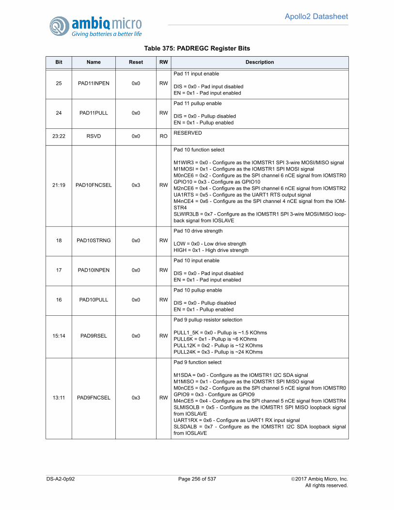
Apollo2 Datasheet
25 PAD11INPEN 0x0 RW
Pad 11 input enable
DIS = 0x0 - Pad input disabledEN = 0x1 - Pad input enabled
24 PAD11PULL 0x0 RW
Pad 11 pullup enable
DIS = 0x0 - Pullup disabledEN = 0x1 - Pullup enabled
23:22 RSVD 0x0 RORESERVED
21:19 PAD10FNCSEL 0x3 RW
Pad 10 function select
M1WIR3 = 0x0 - Configure as the IOMSTR1 SPI 3-wire MOSI/MISO signalM1MOSI = 0x1 - Configure as the IOMSTR1 SPI MOSI signalM0nCE6 = 0x2 - Configure as the SPI channel 6 nCE signal from IOMSTR0GPIO10 = 0x3 - Configure as GPIO10M2nCE6 = 0x4 - Configure as the SPI channel 6 nCE signal from IOMSTR2UA1RTS = 0x5 - Configure as the UART1 RTS output signalM4nCE4 = 0x6 - Configure as the SPI channel 4 nCE signal from the IOM-STR4SLWIR3LB = 0x7 - Configure as the IOMSTR1 SPI 3-wire MOSI/MISO loop-back signal from IOSLAVE
18 PAD10STRNG 0x0 RW
Pad 10 drive strength
LOW = 0x0 - Low drive strengthHIGH = 0x1 - High drive strength
17 PAD10INPEN 0x0 RW
Pad 10 input enable
DIS = 0x0 - Pad input disabledEN = 0x1 - Pad input enabled
16 PAD10PULL 0x0 RW
Pad 10 pullup enable
DIS = 0x0 - Pullup disabledEN = 0x1 - Pullup enabled
15:14 PAD9RSEL 0x0 RW
Pad 9 pullup resistor selection
PULL1_5K = 0x0 - Pullup is ~1.5 KOhmsPULL6K = 0x1 - Pullup is ~6 KOhmsPULL12K = 0x2 - Pullup is ~12 KOhmsPULL24K = 0x3 - Pullup is ~24 KOhms
13:11 PAD9FNCSEL 0x3 RW
Pad 9 function select
M1SDA = 0x0 - Configure as the IOMSTR1 I2C SDA signalM1MISO = 0x1 - Configure as the IOMSTR1 SPI MISO signalM0nCE5 = 0x2 - Configure as the SPI channel 5 nCE signal from IOMSTR0GPIO9 = 0x3 - Configure as GPIO9M4nCE5 = 0x4 - Configure as the SPI channel 5 nCE signal from IOMSTR4SLMISOLB = 0x5 - Configure as the IOMSTR1 SPI MISO loopback signalfrom IOSLAVEUART1RX = 0x6 - Configure as UART1 RX input signalSLSDALB = 0x7 - Configure as the IOMSTR1 I2C SDA loopback signalfrom IOSLAVE
Table 375: PADREGC Register Bits
Bit Name Reset RW Description
DS-A2-0p92 Page 256 of 537 2017 Ambiq Micro, Inc.All rights reserved.
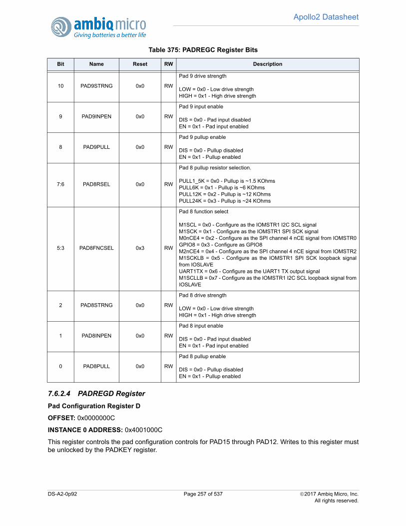
Apollo2 Datasheet
7.6.2.4 PADREGD Register
Pad Configuration Register D
OFFSET: 0x0000000C
INSTANCE 0 ADDRESS: 0x4001000C
This register controls the pad configuration controls for PAD15 through PAD12. Writes to this register mustbe unlocked by the PADKEY register.
10 PAD9STRNG 0x0 RW
Pad 9 drive strength
LOW = 0x0 - Low drive strengthHIGH = 0x1 - High drive strength
9 PAD9INPEN 0x0 RW
Pad 9 input enable
DIS = 0x0 - Pad input disabledEN = 0x1 - Pad input enabled
8 PAD9PULL 0x0 RW
Pad 9 pullup enable
DIS = 0x0 - Pullup disabledEN = 0x1 - Pullup enabled
7:6 PAD8RSEL 0x0 RW
Pad 8 pullup resistor selection.
PULL1_5K = 0x0 - Pullup is ~1.5 KOhmsPULL6K = 0x1 - Pullup is ~6 KOhmsPULL12K = 0x2 - Pullup is ~12 KOhmsPULL24K = 0x3 - Pullup is ~24 KOhms
5:3 PAD8FNCSEL 0x3 RW
Pad 8 function select
M1SCL = 0x0 - Configure as the IOMSTR1 I2C SCL signalM1SCK = 0x1 - Configure as the IOMSTR1 SPI SCK signalM0nCE4 = 0x2 - Configure as the SPI channel 4 nCE signal from IOMSTR0GPIO8 = 0x3 - Configure as GPIO8M2nCE4 = 0x4 - Configure as the SPI channel 4 nCE signal from IOMSTR2M1SCKLB = 0x5 - Configure as the IOMSTR1 SPI SCK loopback signalfrom IOSLAVEUART1TX = 0x6 - Configure as the UART1 TX output signalM1SCLLB = 0x7 - Configure as the IOMSTR1 I2C SCL loopback signal fromIOSLAVE
2 PAD8STRNG 0x0 RW
Pad 8 drive strength
LOW = 0x0 - Low drive strengthHIGH = 0x1 - High drive strength
1 PAD8INPEN 0x0 RW
Pad 8 input enable
DIS = 0x0 - Pad input disabledEN = 0x1 - Pad input enabled
0 PAD8PULL 0x0 RW
Pad 8 pullup enable
DIS = 0x0 - Pullup disabledEN = 0x1 - Pullup enabled
Table 375: PADREGC Register Bits
Bit Name Reset RW Description
DS-A2-0p92 Page 257 of 537 2017 Ambiq Micro, Inc.All rights reserved.

Apollo2 Datasheet
Table 376: PADREGD Register
31
30
29
28
27
26
25
24
23
22
21
20
19
18
17
16
15
14
13
12
11
10
09
08
07
06
05
04
03
02
01
00
RS
VD
PA
D15
FN
C-
SE
L
PA
D15
ST
RN
G
PA
D1
5IN
PE
N
PA
D1
5PU
LL
RS
VD
PA
D14
FN
C-
SE
L
PA
D14
ST
RN
G
PA
D1
4IN
PE
N
PA
D1
4PU
LL
RS
VD
PA
D13
FN
C-
SE
L
PA
D13
ST
RN
G
PA
D1
3IN
PE
N
PA
D1
3PU
LL
RS
VD
PA
D12
FN
C-
SE
L
PA
D12
ST
RN
G
PA
D1
2IN
PE
N
PA
D1
2PU
LL
Table 377: PADREGD Register Bits
Bit Name Reset RW Description
31:30 RSVD 0x0 RORESERVED
29:27 PAD15FNCSEL 0x3 RW
Pad 15 function select
ADCD1N = 0x0 - Configure as the analog ADC differential pair 1 N input sig-nalM1nCE3 = 0x1 - Configure as the SPI channel 3 nCE signal from IOMSTR1UART1RX = 0x2 - Configure as the UART1 RX signalGPIO15 = 0x3 - Configure as GPIO15M2nCE2 = 0x4 - Configure as the SPI Channel 2 nCE signal from IOMSTR2RSV = 0x5 - Function reserved for future useSWDIO = 0x6 - Configure as an alternate port for the SWDIO I/O signalSWO = 0x7 - Configure as an SWO (Serial Wire Trace output)
26 PAD15STRNG 0x0 RW
Pad 15 drive strength
LOW = 0x0 - Low drive strengthHIGH = 0x1 - High drive strength
25 PAD15INPEN 0x0 RW
Pad 15 input enable
DIS = 0x0 - Pad input disabledEN = 0x1 - Pad input enabled
24 PAD15PULL 0x0 RW
Pad 15 pullup enable
DIS = 0x0 - Pullup disabledEN = 0x1 - Pullup enabled
23:22 RSVD 0x0 RORESERVED
21:19 PAD14FNCSEL 0x3 RW
Pad 14 function select
ADCD1P = 0x0 - Configure as the analog ADC differential pair 1 P input sig-nalM1nCE2 = 0x1 - Configure as the SPI channel 2 nCE signal from IOMSTR1UART1TX = 0x2 - Configure as the UART1 TX output signalGPIO14 = 0x3 - Configure as GPIO14M2nCE1 = 0x4 - Configure as the SPI channel 1 nCE signal from IOMSTR2RSV = 0x5 - Function reserved for future useSWDCK = 0x6 - Configure as the alternate input for the SWDCK input signal32khz_XT = 0x7 - Configure as the 32kHz crystal output signal
DS-A2-0p92 Page 258 of 537 2017 Ambiq Micro, Inc.All rights reserved.
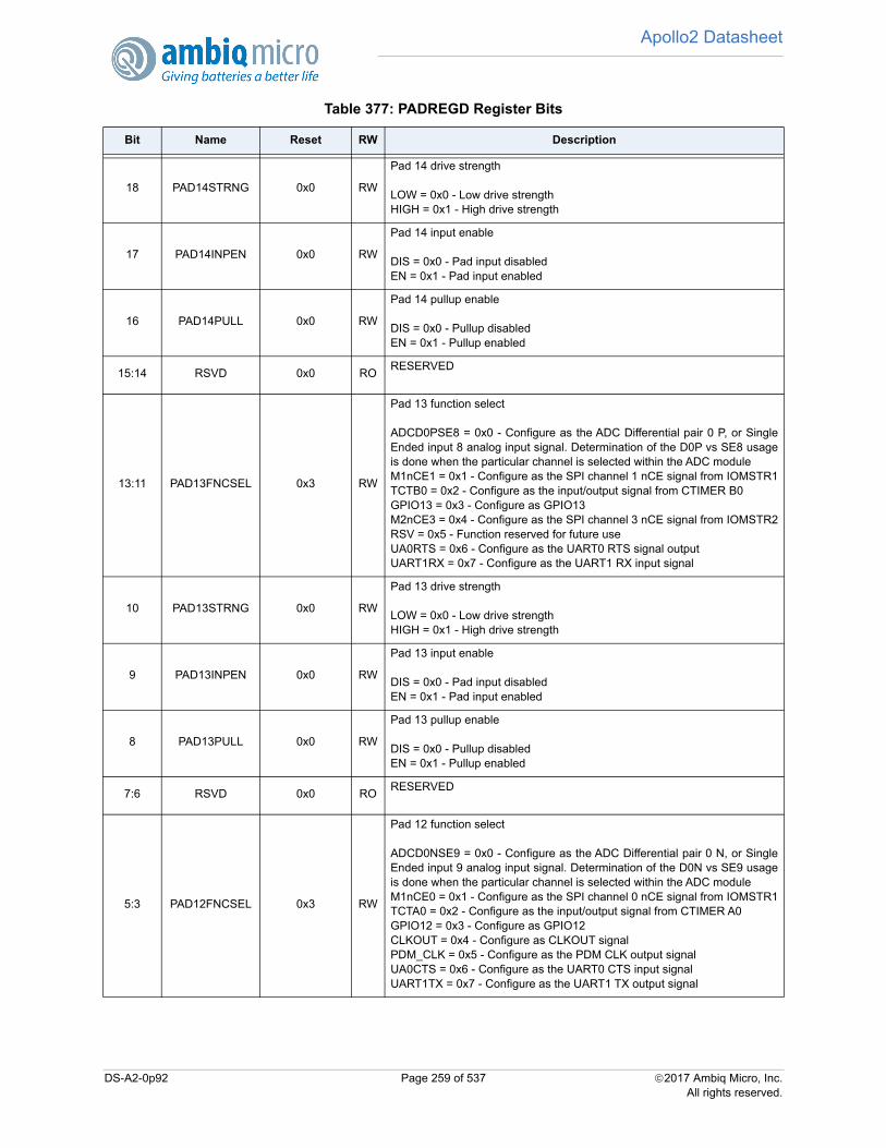
Apollo2 Datasheet
18 PAD14STRNG 0x0 RW
Pad 14 drive strength
LOW = 0x0 - Low drive strengthHIGH = 0x1 - High drive strength
17 PAD14INPEN 0x0 RW
Pad 14 input enable
DIS = 0x0 - Pad input disabledEN = 0x1 - Pad input enabled
16 PAD14PULL 0x0 RW
Pad 14 pullup enable
DIS = 0x0 - Pullup disabledEN = 0x1 - Pullup enabled
15:14 RSVD 0x0 RORESERVED
13:11 PAD13FNCSEL 0x3 RW
Pad 13 function select
ADCD0PSE8 = 0x0 - Configure as the ADC Differential pair 0 P, or SingleEnded input 8 analog input signal. Determination of the D0P vs SE8 usageis done when the particular channel is selected within the ADC moduleM1nCE1 = 0x1 - Configure as the SPI channel 1 nCE signal from IOMSTR1TCTB0 = 0x2 - Configure as the input/output signal from CTIMER B0GPIO13 = 0x3 - Configure as GPIO13M2nCE3 = 0x4 - Configure as the SPI channel 3 nCE signal from IOMSTR2RSV = 0x5 - Function reserved for future useUA0RTS = 0x6 - Configure as the UART0 RTS signal outputUART1RX = 0x7 - Configure as the UART1 RX input signal
10 PAD13STRNG 0x0 RW
Pad 13 drive strength
LOW = 0x0 - Low drive strengthHIGH = 0x1 - High drive strength
9 PAD13INPEN 0x0 RW
Pad 13 input enable
DIS = 0x0 - Pad input disabledEN = 0x1 - Pad input enabled
8 PAD13PULL 0x0 RW
Pad 13 pullup enable
DIS = 0x0 - Pullup disabledEN = 0x1 - Pullup enabled
7:6 RSVD 0x0 RORESERVED
5:3 PAD12FNCSEL 0x3 RW
Pad 12 function select
ADCD0NSE9 = 0x0 - Configure as the ADC Differential pair 0 N, or SingleEnded input 9 analog input signal. Determination of the D0N vs SE9 usageis done when the particular channel is selected within the ADC moduleM1nCE0 = 0x1 - Configure as the SPI channel 0 nCE signal from IOMSTR1TCTA0 = 0x2 - Configure as the input/output signal from CTIMER A0GPIO12 = 0x3 - Configure as GPIO12CLKOUT = 0x4 - Configure as CLKOUT signalPDM_CLK = 0x5 - Configure as the PDM CLK output signalUA0CTS = 0x6 - Configure as the UART0 CTS input signalUART1TX = 0x7 - Configure as the UART1 TX output signal
Table 377: PADREGD Register Bits
Bit Name Reset RW Description
DS-A2-0p92 Page 259 of 537 2017 Ambiq Micro, Inc.All rights reserved.
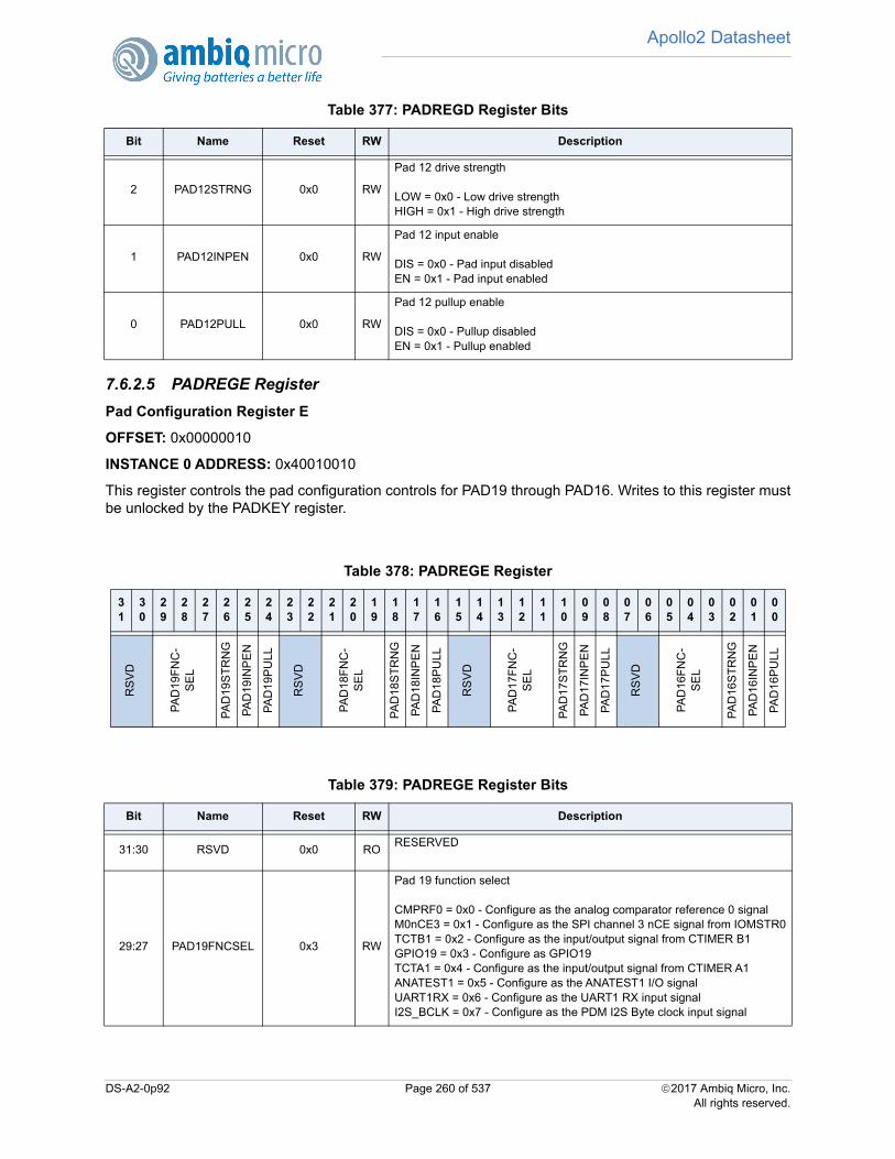
Apollo2 Datasheet
7.6.2.5 PADREGE Register
Pad Configuration Register E
OFFSET: 0x00000010
INSTANCE 0 ADDRESS: 0x40010010
This register controls the pad configuration controls for PAD19 through PAD16. Writes to this register mustbe unlocked by the PADKEY register.
2 PAD12STRNG 0x0 RW
Pad 12 drive strength
LOW = 0x0 - Low drive strengthHIGH = 0x1 - High drive strength
1 PAD12INPEN 0x0 RW
Pad 12 input enable
DIS = 0x0 - Pad input disabledEN = 0x1 - Pad input enabled
0 PAD12PULL 0x0 RW
Pad 12 pullup enable
DIS = 0x0 - Pullup disabledEN = 0x1 - Pullup enabled
Table 378: PADREGE Register
31
30
29
28
27
26
25
24
23
22
21
20
19
18
17
16
15
14
13
12
11
10
09
08
07
06
05
04
03
02
01
00
RS
VD
PA
D19
FN
C-
SE
L
PA
D19
ST
RN
G
PA
D19
INP
EN
PA
D19
PU
LL
RS
VD
PA
D18
FN
C-
SE
L
PA
D18
ST
RN
G
PA
D18
INP
EN
PA
D18
PU
LL
RS
VD
PA
D17
FN
C-
SE
L
PA
D17
ST
RN
G
PA
D17
INP
EN
PA
D17
PU
LL
RS
VD
PA
D16
FN
C-
SE
L
PA
D16
ST
RN
G
PA
D16
INP
EN
PA
D16
PU
LLTable 379: PADREGE Register Bits
Bit Name Reset RW Description
31:30 RSVD 0x0 RORESERVED
29:27 PAD19FNCSEL 0x3 RW
Pad 19 function select
CMPRF0 = 0x0 - Configure as the analog comparator reference 0 signalM0nCE3 = 0x1 - Configure as the SPI channel 3 nCE signal from IOMSTR0TCTB1 = 0x2 - Configure as the input/output signal from CTIMER B1GPIO19 = 0x3 - Configure as GPIO19TCTA1 = 0x4 - Configure as the input/output signal from CTIMER A1ANATEST1 = 0x5 - Configure as the ANATEST1 I/O signalUART1RX = 0x6 - Configure as the UART1 RX input signalI2S_BCLK = 0x7 - Configure as the PDM I2S Byte clock input signal
Table 377: PADREGD Register Bits
Bit Name Reset RW Description
DS-A2-0p92 Page 260 of 537 2017 Ambiq Micro, Inc.All rights reserved.
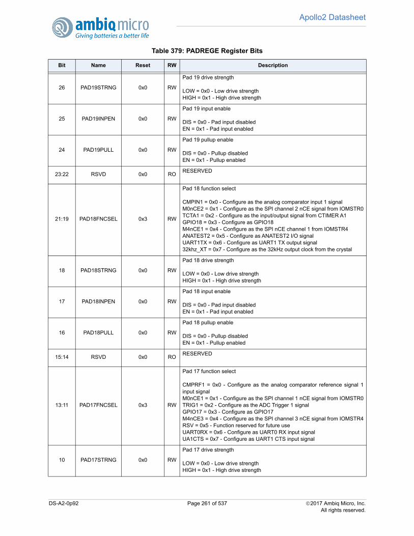
Apollo2 Datasheet
26 PAD19STRNG 0x0 RW
Pad 19 drive strength
LOW = 0x0 - Low drive strengthHIGH = 0x1 - High drive strength
25 PAD19INPEN 0x0 RW
Pad 19 input enable
DIS = 0x0 - Pad input disabledEN = 0x1 - Pad input enabled
24 PAD19PULL 0x0 RW
Pad 19 pullup enable
DIS = 0x0 - Pullup disabledEN = 0x1 - Pullup enabled
23:22 RSVD 0x0 RORESERVED
21:19 PAD18FNCSEL 0x3 RW
Pad 18 function select
CMPIN1 = 0x0 - Configure as the analog comparator input 1 signalM0nCE2 = 0x1 - Configure as the SPI channel 2 nCE signal from IOMSTR0TCTA1 = 0x2 - Configure as the input/output signal from CTIMER A1GPIO18 = 0x3 - Configure as GPIO18M4nCE1 = 0x4 - Configure as the SPI nCE channel 1 from IOMSTR4ANATEST2 = 0x5 - Configure as ANATEST2 I/O signalUART1TX = 0x6 - Configure as UART1 TX output signal32khz_XT = 0x7 - Configure as the 32kHz output clock from the crystal
18 PAD18STRNG 0x0 RW
Pad 18 drive strength
LOW = 0x0 - Low drive strengthHIGH = 0x1 - High drive strength
17 PAD18INPEN 0x0 RW
Pad 18 input enable
DIS = 0x0 - Pad input disabledEN = 0x1 - Pad input enabled
16 PAD18PULL 0x0 RW
Pad 18 pullup enable
DIS = 0x0 - Pullup disabledEN = 0x1 - Pullup enabled
15:14 RSVD 0x0 RORESERVED
13:11 PAD17FNCSEL 0x3 RW
Pad 17 function select
CMPRF1 = 0x0 - Configure as the analog comparator reference signal 1input signalM0nCE1 = 0x1 - Configure as the SPI channel 1 nCE signal from IOMSTR0TRIG1 = 0x2 - Configure as the ADC Trigger 1 signalGPIO17 = 0x3 - Configure as GPIO17M4nCE3 = 0x4 - Configure as the SPI channel 3 nCE signal from IOMSTR4RSV = 0x5 - Function reserved for future useUART0RX = 0x6 - Configure as UART0 RX input signalUA1CTS = 0x7 - Configure as UART1 CTS input signal
10 PAD17STRNG 0x0 RW
Pad 17 drive strength
LOW = 0x0 - Low drive strengthHIGH = 0x1 - High drive strength
Table 379: PADREGE Register Bits
Bit Name Reset RW Description
DS-A2-0p92 Page 261 of 537 2017 Ambiq Micro, Inc.All rights reserved.

Apollo2 Datasheet
7.6.2.6 PADREGF Register
Pad Configuration Register F
OFFSET: 0x00000014
INSTANCE 0 ADDRESS: 0x40010014
This register controls the pad configuration controls for PAD23 through PAD20. Writes to this register mustbe unlocked by the PADKEY register.
9 PAD17INPEN 0x0 RW
Pad 17 input enable
DIS = 0x0 - Pad input disabledEN = 0x1 - Pad input enabled
8 PAD17PULL 0x0 RW
Pad 17 pullup enable
DIS = 0x0 - Pullup disabledEN = 0x1 - Pullup enabled
7:6 RSVD 0x0 RORESERVED
5:3 PAD16FNCSEL 0x3 RW
Pad 16 function select
ADCSE0 = 0x0 - Configure as the analog ADC single ended port 0 input sig-nalM0nCE4 = 0x1 - Configure as the SPI channel 4 nCE signal from IOMSTR0TRIG0 = 0x2 - Configure as the ADC Trigger 0 signalGPIO16 = 0x3 - Configure as GPIO16M2nCE3 = 0x4 - Configure as SPI channel 3 nCE for IOMSTR2CMPIN0 = 0x5 - Configure as comparator input 0 signalUART0TX = 0x6 - Configure as UART0 TX output signalUA1RTS = 0x7 - Configure as UART1 RTS output signal
2 PAD16STRNG 0x0 RW
Pad 16 drive strength
LOW = 0x0 - Low drive strengthHIGH = 0x1 - High drive strength
1 PAD16INPEN 0x0 RW
Pad 16 input enable
DIS = 0x0 - Pad input disabledEN = 0x1 - Pad input enabled
0 PAD16PULL 0x0 RW
Pad 16 pullup enable
DIS = 0x0 - Pullup disabledEN = 0x1 - Pullup enabled
Table 379: PADREGE Register Bits
Bit Name Reset RW Description
DS-A2-0p92 Page 262 of 537 2017 Ambiq Micro, Inc.All rights reserved.
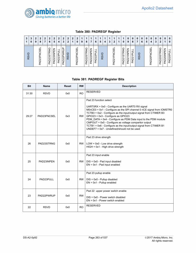
Apollo2 Datasheet
Table 380: PADREGF Register
31
30
29
28
27
26
25
24
23
22
21
20
19
18
17
16
15
14
13
12
11
10
09
08
07
06
05
04
03
02
01
00
RS
VD
PA
D23
FN
CS
EL
PA
D23
ST
RN
G
PA
D2
3IN
PE
N
PA
D2
3PU
LL
PA
D22
PW
RU
P
RS
VD
PA
D22
FN
CS
EL
PA
D22
ST
RN
G
PA
D2
2IN
PE
N
PA
D2
2PU
LL
RS
VD
PA
D21
FN
CS
EL
PA
D21
ST
RN
G
PA
D2
1IN
PE
N
PA
D2
1PU
LL
RS
VD
PA
D20
FN
CS
EL
PA
D20
ST
RN
G
PA
D2
0IN
PE
N
PA
D2
0PU
LL
Table 381: PADREGF Register Bits
Bit Name Reset RW Description
31:30 RSVD 0x0 RORESERVED
29:27 PAD23FNCSEL 0x3 RW
Pad 23 function select
UART0RX = 0x0 - Configure as the UART0 RX signalM0nCE0 = 0x1 - Configure as the SPI channel 0 nCE signal from IOMSTR0TCTB3 = 0x2 - Configure as the input/output signal from CTIMER B3GPIO23 = 0x3 - Configure as GPIO23PDM_DATA = 0x4 - Configure as PDM Data input to the PDM moduleCMPOUT = 0x5 - Configure as voltage comparitor outputTCTB1 = 0x6 - Configure as the input/output signal from CTIMER B1UNDEF7 = 0x7 - Undefined/should not be used
26 PAD23STRNG 0x0 RW
Pad 23 drive strength
LOW = 0x0 - Low drive strengthHIGH = 0x1 - High drive strength
25 PAD23INPEN 0x0 RW
Pad 23 input enable
DIS = 0x0 - Pad input disabledEN = 0x1 - Pad input enabled
24 PAD23PULL 0x0 RW
Pad 23 pullup enable
DIS = 0x0 - Pullup disabledEN = 0x1 - Pullup enabled
23 PAD22PWRUP 0x0 RW
Pad 22 upper power switch enable
DIS = 0x0 - Power switch disabledEN = 0x1 - Power switch enabled
22 RSVD 0x0 RORESERVED
DS-A2-0p92 Page 263 of 537 2017 Ambiq Micro, Inc.All rights reserved.
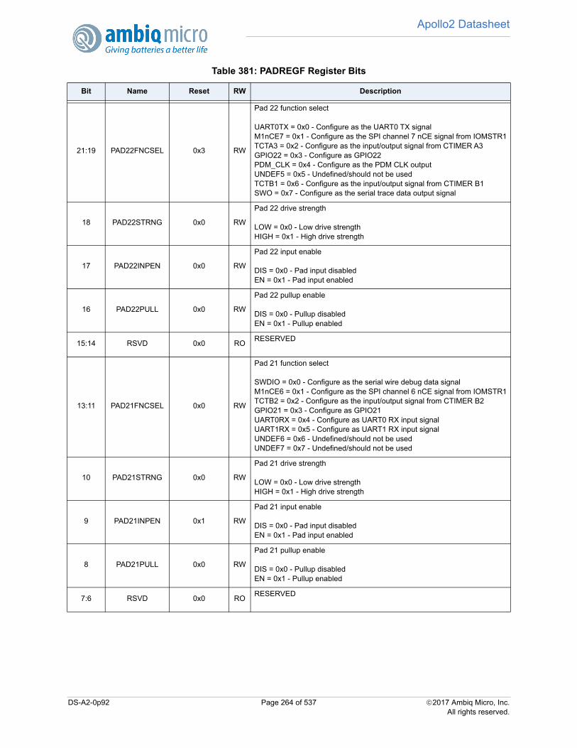
Apollo2 Datasheet
21:19 PAD22FNCSEL 0x3 RW
Pad 22 function select
UART0TX = 0x0 - Configure as the UART0 TX signalM1nCE7 = 0x1 - Configure as the SPI channel 7 nCE signal from IOMSTR1TCTA3 = 0x2 - Configure as the input/output signal from CTIMER A3GPIO22 = 0x3 - Configure as GPIO22PDM_CLK = 0x4 - Configure as the PDM CLK outputUNDEF5 = 0x5 - Undefined/should not be usedTCTB1 = 0x6 - Configure as the input/output signal from CTIMER B1SWO = 0x7 - Configure as the serial trace data output signal
18 PAD22STRNG 0x0 RW
Pad 22 drive strength
LOW = 0x0 - Low drive strengthHIGH = 0x1 - High drive strength
17 PAD22INPEN 0x0 RW
Pad 22 input enable
DIS = 0x0 - Pad input disabledEN = 0x1 - Pad input enabled
16 PAD22PULL 0x0 RW
Pad 22 pullup enable
DIS = 0x0 - Pullup disabledEN = 0x1 - Pullup enabled
15:14 RSVD 0x0 RORESERVED
13:11 PAD21FNCSEL 0x0 RW
Pad 21 function select
SWDIO = 0x0 - Configure as the serial wire debug data signalM1nCE6 = 0x1 - Configure as the SPI channel 6 nCE signal from IOMSTR1TCTB2 = 0x2 - Configure as the input/output signal from CTIMER B2GPIO21 = 0x3 - Configure as GPIO21UART0RX = 0x4 - Configure as UART0 RX input signalUART1RX = 0x5 - Configure as UART1 RX input signalUNDEF6 = 0x6 - Undefined/should not be usedUNDEF7 = 0x7 - Undefined/should not be used
10 PAD21STRNG 0x0 RW
Pad 21 drive strength
LOW = 0x0 - Low drive strengthHIGH = 0x1 - High drive strength
9 PAD21INPEN 0x1 RW
Pad 21 input enable
DIS = 0x0 - Pad input disabledEN = 0x1 - Pad input enabled
8 PAD21PULL 0x0 RW
Pad 21 pullup enable
DIS = 0x0 - Pullup disabledEN = 0x1 - Pullup enabled
7:6 RSVD 0x0 RORESERVED
Table 381: PADREGF Register Bits
Bit Name Reset RW Description
DS-A2-0p92 Page 264 of 537 2017 Ambiq Micro, Inc.All rights reserved.
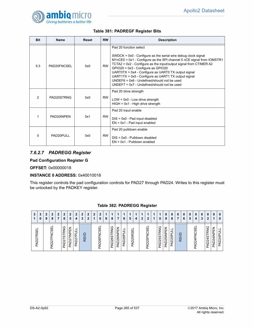
Apollo2 Datasheet
7.6.2.7 PADREGG Register
Pad Configuration Register G
OFFSET: 0x00000018
INSTANCE 0 ADDRESS: 0x40010018
This register controls the pad configuration controls for PAD27 through PAD24. Writes to this register mustbe unlocked by the PADKEY register.
5:3 PAD20FNCSEL 0x0 RW
Pad 20 function select
SWDCK = 0x0 - Configure as the serial wire debug clock signalM1nCE5 = 0x1 - Configure as the SPI channel 5 nCE signal from IOMSTR1TCTA2 = 0x2 - Configure as the input/output signal from CTIMER A2GPIO20 = 0x3 - Configure as GPIO20UART0TX = 0x4 - Configure as UART0 TX output signalUART1TX = 0x5 - Configure as UART1 TX output signalUNDEF6 = 0x6 - Undefined/should not be usedUNDEF7 = 0x7 - Undefined/should not be used
2 PAD20STRNG 0x0 RW
Pad 20 drive strength
LOW = 0x0 - Low drive strengthHIGH = 0x1 - High drive strength
1 PAD20INPEN 0x1 RW
Pad 20 input enable
DIS = 0x0 - Pad input disabledEN = 0x1 - Pad input enabled
0 PAD20PULL 0x0 RW
Pad 20 pulldown enable
DIS = 0x0 - Pulldown disabledEN = 0x1 - Pulldown enabled
Table 382: PADREGG Register
31
30
29
28
27
26
25
24
23
22
21
20
19
18
17
16
15
14
13
12
11
10
09
08
07
06
05
04
03
02
01
00
PA
D27
RS
EL
PA
D27
FN
CS
EL
PA
D27
ST
RN
G
PA
D27
INP
EN
PA
D27
PU
LL
RS
VD
PA
D26
FN
CS
EL
PA
D26
ST
RN
G
PA
D26
INP
EN
PA
D26
PU
LL
PA
D25
RS
EL
PA
D25
FN
CS
EL
PA
D25
ST
RN
G
PA
D25
INP
EN
PA
D25
PU
LL
RS
VD
PA
D24
FN
CS
EL
PA
D24
ST
RN
G
PA
D24
INP
EN
PA
D24
PU
LL
Table 381: PADREGF Register Bits
Bit Name Reset RW Description
DS-A2-0p92 Page 265 of 537 2017 Ambiq Micro, Inc.All rights reserved.
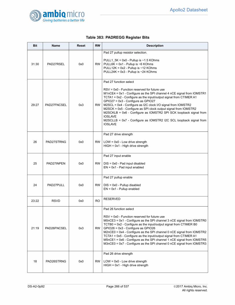
Apollo2 Datasheet
Table 383: PADREGG Register Bits
Bit Name Reset RW Description
31:30 PAD27RSEL 0x0 RW
Pad 27 pullup resistor selection.
PULL1_5K = 0x0 - Pullup is ~1.5 KOhmsPULL6K = 0x1 - Pullup is ~6 KOhmsPULL12K = 0x2 - Pullup is ~12 KOhmsPULL24K = 0x3 - Pullup is ~24 KOhms
29:27 PAD27FNCSEL 0x3 RW
Pad 27 function select
RSV = 0x0 - Function reserved for future useM1nCE4 = 0x1 - Configure as the SPI channel 4 nCE signal from IOMSTR1TCTA1 = 0x2 - Configure as the input/output signal from CTIMER A1GPIO27 = 0x3 - Configure as GPIO27M2SCL = 0x4 - Configure as I2C clock I/O signal from IOMSTR2M2SCK = 0x5 - Configure as SPI clock output signal from IOMSTR2M2SCKLB = 0x6 - Configure as IOMSTR2 SPI SCK loopback signal fromIOSLAVEM2SCLLB = 0x7 - Configure as IOMSTR2 I2C SCL loopback signal fromIOSLAVE
26 PAD27STRNG 0x0 RW
Pad 27 drive strength
LOW = 0x0 - Low drive strengthHIGH = 0x1 - High drive strength
25 PAD27INPEN 0x0 RW
Pad 27 input enable
DIS = 0x0 - Pad input disabledEN = 0x1 - Pad input enabled
24 PAD27PULL 0x0 RW
Pad 27 pullup enable
DIS = 0x0 - Pullup disabledEN = 0x1 - Pullup enabled
23:22 RSVD 0x0 RORESERVED
21:19 PAD26FNCSEL 0x3 RW
Pad 26 function select
RSV = 0x0 - Function reserved for future useM0nCE3 = 0x1 - Configure as the SPI channel 3 nCE signal from IOMSTR0TCTB0 = 0x2 - Configure as the input/output signal from CTIMER B0GPIO26 = 0x3 - Configure as GPIO26M2nCE0 = 0x4 - Configure as the SPI channel 0 nCE signal from IOMSTR2TCTA1 = 0x5 - Configure as the input/output signal from CTIMER A1M5nCE1 = 0x6 - Configure as the SPI channel 1 nCE signal from IOMSTR5M3nCE0 = 0x7 - Configure as the SPI channel 0 nCE signal from IOMSTR3
18 PAD26STRNG 0x0 RW
Pad 26 drive strength
LOW = 0x0 - Low drive strengthHIGH = 0x1 - High drive strength
DS-A2-0p92 Page 266 of 537 2017 Ambiq Micro, Inc.All rights reserved.

Apollo2 Datasheet
17 PAD26INPEN 0x0 RW
Pad 26 input enable
DIS = 0x0 - Pad input disabledEN = 0x1 - Pad input enabled
16 PAD26PULL 0x0 RW
Pad 26 pullup enable
DIS = 0x0 - Pullup disabledEN = 0x1 - Pullup enabled
15:14 PAD25RSEL 0x0 RW
Pad 25 pullup resistor selection.
PULL1_5K = 0x0 - Pullup is ~1.5 KOhmsPULL6K = 0x1 - Pullup is ~6 KOhmsPULL12K = 0x2 - Pullup is ~12 KOhmsPULL24K = 0x3 - Pullup is ~24 KOhms
13:11 PAD25FNCSEL 0x3 RW
Pad 25 function select
RSV = 0x0 - Function reserved for future useM0nCE2 = 0x1 - Configure as the SPI channel 2 nCE signal from IOMSTR0TCTA0 = 0x2 - Configure as the input/output signal from CTIMER A0GPIO25 = 0x3 - Configure as GPIO25M2SDA = 0x4 - Configure as the IOMSTR2 I2C Serial data I/O signalM2MISO = 0x5 - Configure as the IOMSTR2 SPI MISO input signalSLMISOLB = 0x6 - Configure as the IOMSTR0 SPI MISO loopback signalfrom IOSLAVESLSDALB = 0x7 - Configure as the IOMSTR0 I2C SDA loopback signalfrom IOSLAVE
10 PAD25STRNG 0x0 RW
Pad 25 drive strength
LOW = 0x0 - Low drive strengthHIGH = 0x1 - High drive strength
9 PAD25INPEN 0x0 RW
Pad 25 input enable
DIS = 0x0 - Pad input disabledEN = 0x1 - Pad input enabled
8 PAD25PULL 0x0 RW
Pad 25 pullup enable
DIS = 0x0 - Pullup disabledEN = 0x1 - Pullup enabled
7:6 RSVD 0x0 RORESERVED
Table 383: PADREGG Register Bits
Bit Name Reset RW Description
DS-A2-0p92 Page 267 of 537 2017 Ambiq Micro, Inc.All rights reserved.
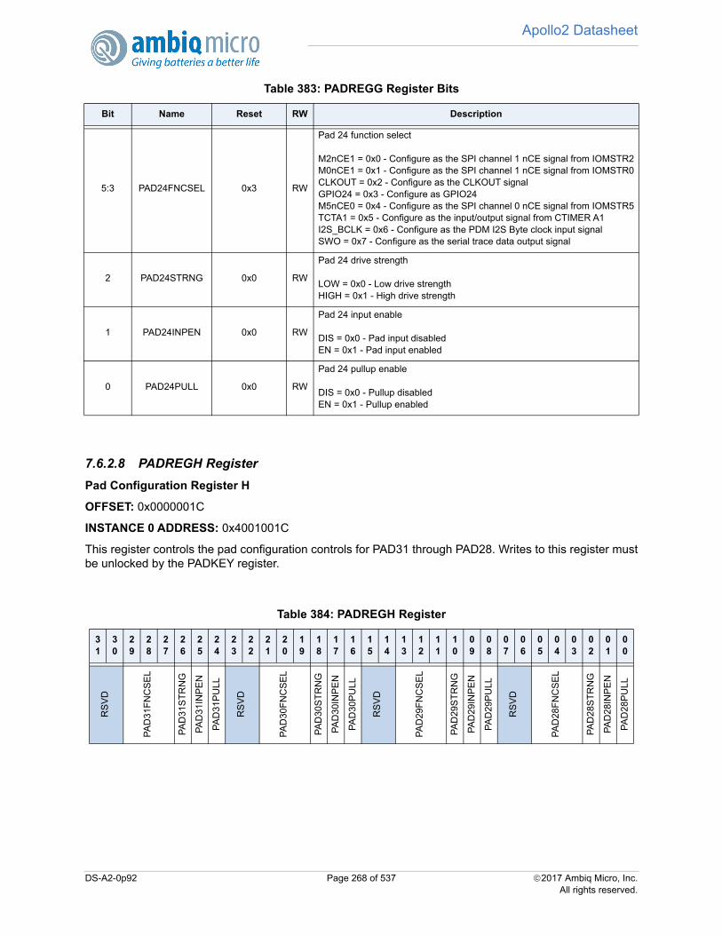
Apollo2 Datasheet
7.6.2.8 PADREGH Register
Pad Configuration Register H
OFFSET: 0x0000001C
INSTANCE 0 ADDRESS: 0x4001001C
This register controls the pad configuration controls for PAD31 through PAD28. Writes to this register mustbe unlocked by the PADKEY register.
5:3 PAD24FNCSEL 0x3 RW
Pad 24 function select
M2nCE1 = 0x0 - Configure as the SPI channel 1 nCE signal from IOMSTR2M0nCE1 = 0x1 - Configure as the SPI channel 1 nCE signal from IOMSTR0CLKOUT = 0x2 - Configure as the CLKOUT signalGPIO24 = 0x3 - Configure as GPIO24M5nCE0 = 0x4 - Configure as the SPI channel 0 nCE signal from IOMSTR5TCTA1 = 0x5 - Configure as the input/output signal from CTIMER A1I2S_BCLK = 0x6 - Configure as the PDM I2S Byte clock input signalSWO = 0x7 - Configure as the serial trace data output signal
2 PAD24STRNG 0x0 RW
Pad 24 drive strength
LOW = 0x0 - Low drive strengthHIGH = 0x1 - High drive strength
1 PAD24INPEN 0x0 RW
Pad 24 input enable
DIS = 0x0 - Pad input disabledEN = 0x1 - Pad input enabled
0 PAD24PULL 0x0 RW
Pad 24 pullup enable
DIS = 0x0 - Pullup disabledEN = 0x1 - Pullup enabled
Table 384: PADREGH Register
31
30
29
28
27
26
25
24
23
22
21
20
19
18
17
16
15
14
13
12
11
10
09
08
07
06
05
04
03
02
01
00
RS
VD
PA
D31
FN
CS
EL
PA
D31
ST
RN
G
PA
D31
INP
EN
PA
D31
PU
LL
RS
VD
PA
D30
FN
CS
EL
PA
D30
ST
RN
G
PA
D30
INP
EN
PA
D30
PU
LL
RS
VD
PA
D29
FN
CS
EL
PA
D29
ST
RN
G
PA
D29
INP
EN
PA
D29
PU
LL
RS
VD
PA
D28
FN
CS
EL
PA
D28
ST
RN
G
PA
D28
INP
EN
PA
D28
PU
LL
Table 383: PADREGG Register Bits
Bit Name Reset RW Description
DS-A2-0p92 Page 268 of 537 2017 Ambiq Micro, Inc.All rights reserved.

Apollo2 Datasheet
Table 385: PADREGH Register Bits
Bit Name Reset RW Description
31:30 RSVD 0x0 RORESERVED
29:27 PAD31FNCSEL 0x3 RW
Pad 31 function select
ADCSE3 = 0x0 - Configure as the analog input for ADC single ended input 3M0nCE4 = 0x1 - Configure as the SPI channel 4 nCE signal from IOMSTR0TCTA3 = 0x2 - Configure as the input/output signal from CTIMER A3GPIO31 = 0x3 - Configure as GPIO31UART0RX = 0x4 - Configure as the UART0 RX input signalTCTB1 = 0x5 - Configure as the input/output signal from CTIMER B1UNDEF6 = 0x6 - Undefined/should not be usedUNDEF7 = 0x7 - Undefined/should not be used
26 PAD31STRNG 0x0 RW
Pad 31 drive strength
LOW = 0x0 - Low drive strengthHIGH = 0x1 - High drive strength
25 PAD31INPEN 0x0 RW
Pad 31 input enable
DIS = 0x0 - Pad input disabledEN = 0x1 - Pad input enabled
24 PAD31PULL 0x0 RW
Pad 31 pullup enable
DIS = 0x0 - Pullup disabledEN = 0x1 - Pullup enabled
23:22 RSVD 0x0 RORESERVED
21:19 PAD30FNCSEL 0x3 RW
Pad 30 function select
UNDEF0 = 0x0 - Undefined/should not be usedM1nCE7 = 0x1 - Configure as the SPI channel 7 nCE signal from IOMSTR1TCTB2 = 0x2 - Configure as the input/output signal from CTIMER B2GPIO30 = 0x3 - Configure as GPIO30UART0TX = 0x4 - Configure as UART0 TX output signalUA1RTS = 0x5 - Configure as UART1 RTS output signalUNDEF6 = 0x6 - Undefined/should not be usedI2S_DAT = 0x7 - Configure as the PDM I2S Data output signal
18 PAD30STRNG 0x0 RW
Pad 30 drive strength
LOW = 0x0 - Low drive strengthHIGH = 0x1 - High drive strength
17 PAD30INPEN 0x0 RW
Pad 30 input enable
DIS = 0x0 - Pad input disabledEN = 0x1 - Pad input enabled
16 PAD30PULL 0x0 RW
Pad 30 pullup enable
DIS = 0x0 - Pullup disabledEN = 0x1 - Pullup enabled
DS-A2-0p92 Page 269 of 537 2017 Ambiq Micro, Inc.All rights reserved.
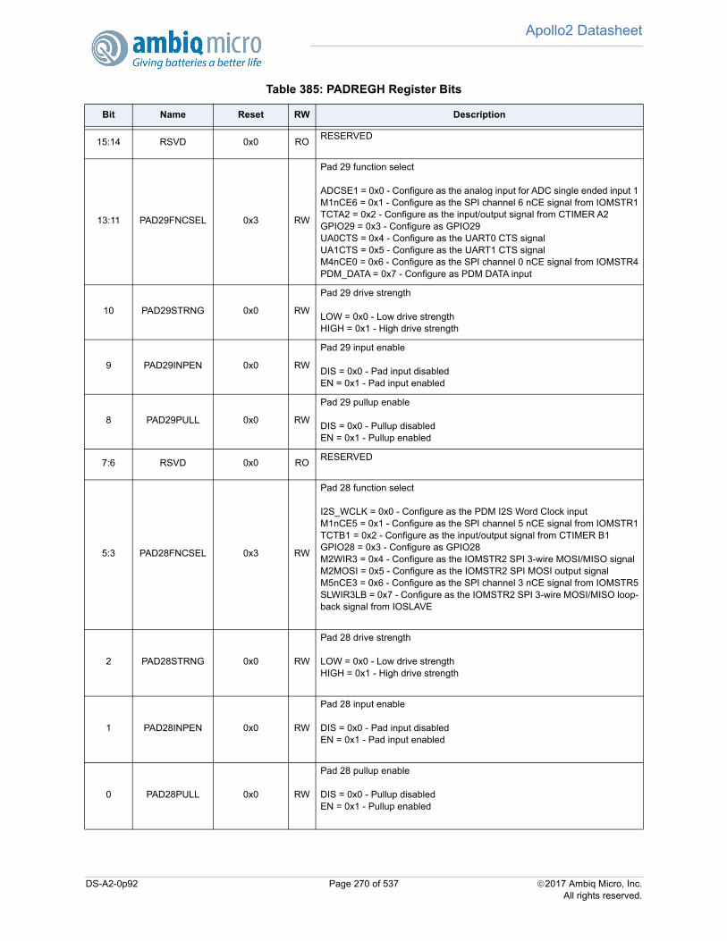
Apollo2 Datasheet
15:14 RSVD 0x0 RORESERVED
13:11 PAD29FNCSEL 0x3 RW
Pad 29 function select
ADCSE1 = 0x0 - Configure as the analog input for ADC single ended input 1M1nCE6 = 0x1 - Configure as the SPI channel 6 nCE signal from IOMSTR1TCTA2 = 0x2 - Configure as the input/output signal from CTIMER A2GPIO29 = 0x3 - Configure as GPIO29UA0CTS = 0x4 - Configure as the UART0 CTS signalUA1CTS = 0x5 - Configure as the UART1 CTS signalM4nCE0 = 0x6 - Configure as the SPI channel 0 nCE signal from IOMSTR4PDM_DATA = 0x7 - Configure as PDM DATA input
10 PAD29STRNG 0x0 RW
Pad 29 drive strength
LOW = 0x0 - Low drive strengthHIGH = 0x1 - High drive strength
9 PAD29INPEN 0x0 RW
Pad 29 input enable
DIS = 0x0 - Pad input disabledEN = 0x1 - Pad input enabled
8 PAD29PULL 0x0 RW
Pad 29 pullup enable
DIS = 0x0 - Pullup disabledEN = 0x1 - Pullup enabled
7:6 RSVD 0x0 RORESERVED
5:3 PAD28FNCSEL 0x3 RW
Pad 28 function select
I2S_WCLK = 0x0 - Configure as the PDM I2S Word Clock inputM1nCE5 = 0x1 - Configure as the SPI channel 5 nCE signal from IOMSTR1TCTB1 = 0x2 - Configure as the input/output signal from CTIMER B1GPIO28 = 0x3 - Configure as GPIO28M2WIR3 = 0x4 - Configure as the IOMSTR2 SPI 3-wire MOSI/MISO signalM2MOSI = 0x5 - Configure as the IOMSTR2 SPI MOSI output signalM5nCE3 = 0x6 - Configure as the SPI channel 3 nCE signal from IOMSTR5SLWIR3LB = 0x7 - Configure as the IOMSTR2 SPI 3-wire MOSI/MISO loop-back signal from IOSLAVE
2 PAD28STRNG 0x0 RW
Pad 28 drive strength
LOW = 0x0 - Low drive strengthHIGH = 0x1 - High drive strength
1 PAD28INPEN 0x0 RW
Pad 28 input enable
DIS = 0x0 - Pad input disabledEN = 0x1 - Pad input enabled
0 PAD28PULL 0x0 RW
Pad 28 pullup enable
DIS = 0x0 - Pullup disabledEN = 0x1 - Pullup enabled
Table 385: PADREGH Register Bits
Bit Name Reset RW Description
DS-A2-0p92 Page 270 of 537 2017 Ambiq Micro, Inc.All rights reserved.
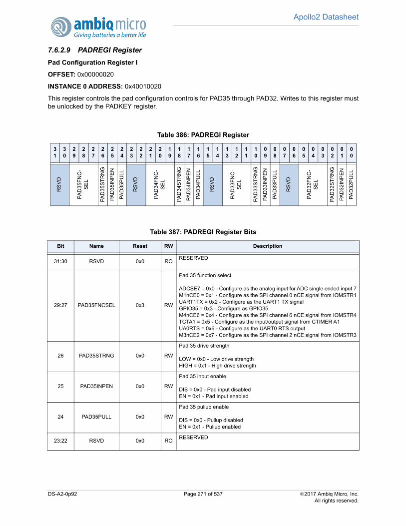
Apollo2 Datasheet
7.6.2.9 PADREGI Register
Pad Configuration Register I
OFFSET: 0x00000020
INSTANCE 0 ADDRESS: 0x40010020
This register controls the pad configuration controls for PAD35 through PAD32. Writes to this register mustbe unlocked by the PADKEY register.
Table 386: PADREGI Register
31
30
29
28
27
26
25
24
23
22
21
20
19
18
17
16
15
14
13
12
11
10
09
08
07
06
05
04
03
02
01
00
RS
VD
PA
D35
FN
C-
SE
L
PA
D35
ST
RN
G
PA
D35
INP
EN
PA
D35
PU
LL
RS
VD
PA
D34
FN
C-
SE
L
PA
D34
ST
RN
G
PA
D34
INP
EN
PA
D34
PU
LL
RS
VD
PA
D33
FN
C-
SE
L
PA
D33
ST
RN
G
PA
D33
INP
EN
PA
D33
PU
LL
RS
VD
PA
D32
FN
C-
SE
L
PA
D32
ST
RN
G
PA
D32
INP
EN
PA
D32
PU
LL
Table 387: PADREGI Register Bits
Bit Name Reset RW Description
31:30 RSVD 0x0 RORESERVED
29:27 PAD35FNCSEL 0x3 RW
Pad 35 function select
ADCSE7 = 0x0 - Configure as the analog input for ADC single ended input 7M1nCE0 = 0x1 - Configure as the SPI channel 0 nCE signal from IOMSTR1UART1TX = 0x2 - Configure as the UART1 TX signalGPIO35 = 0x3 - Configure as GPIO35M4nCE6 = 0x4 - Configure as the SPI channel 6 nCE signal from IOMSTR4TCTA1 = 0x5 - Configure as the input/output signal from CTIMER A1UA0RTS = 0x6 - Configure as the UART0 RTS outputM3nCE2 = 0x7 - Configure as the SPI channel 2 nCE signal from IOMSTR3
26 PAD35STRNG 0x0 RW
Pad 35 drive strength
LOW = 0x0 - Low drive strengthHIGH = 0x1 - High drive strength
25 PAD35INPEN 0x0 RW
Pad 35 input enable
DIS = 0x0 - Pad input disabledEN = 0x1 - Pad input enabled
24 PAD35PULL 0x0 RW
Pad 35 pullup enable
DIS = 0x0 - Pullup disabledEN = 0x1 - Pullup enabled
23:22 RSVD 0x0 RORESERVED
DS-A2-0p92 Page 271 of 537 2017 Ambiq Micro, Inc.All rights reserved.
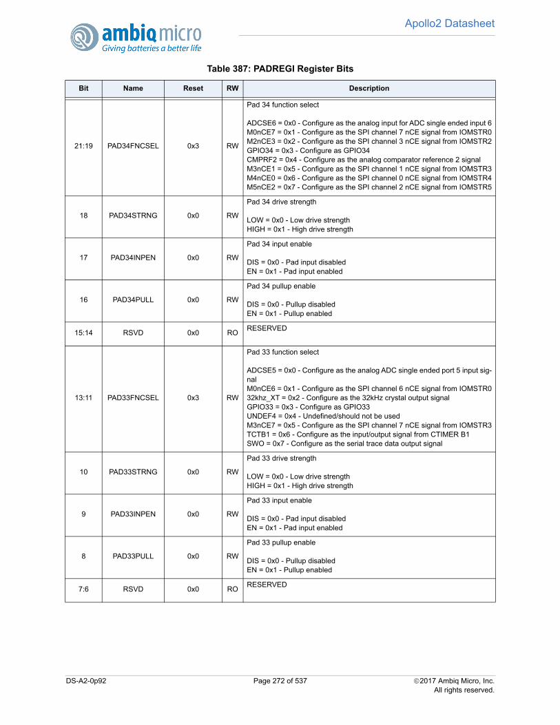
Apollo2 Datasheet
21:19 PAD34FNCSEL 0x3 RW
Pad 34 function select
ADCSE6 = 0x0 - Configure as the analog input for ADC single ended input 6M0nCE7 = 0x1 - Configure as the SPI channel 7 nCE signal from IOMSTR0M2nCE3 = 0x2 - Configure as the SPI channel 3 nCE signal from IOMSTR2GPIO34 = 0x3 - Configure as GPIO34CMPRF2 = 0x4 - Configure as the analog comparator reference 2 signalM3nCE1 = 0x5 - Configure as the SPI channel 1 nCE signal from IOMSTR3M4nCE0 = 0x6 - Configure as the SPI channel 0 nCE signal from IOMSTR4M5nCE2 = 0x7 - Configure as the SPI channel 2 nCE signal from IOMSTR5
18 PAD34STRNG 0x0 RW
Pad 34 drive strength
LOW = 0x0 - Low drive strengthHIGH = 0x1 - High drive strength
17 PAD34INPEN 0x0 RW
Pad 34 input enable
DIS = 0x0 - Pad input disabledEN = 0x1 - Pad input enabled
16 PAD34PULL 0x0 RW
Pad 34 pullup enable
DIS = 0x0 - Pullup disabledEN = 0x1 - Pullup enabled
15:14 RSVD 0x0 RORESERVED
13:11 PAD33FNCSEL 0x3 RW
Pad 33 function select
ADCSE5 = 0x0 - Configure as the analog ADC single ended port 5 input sig-nalM0nCE6 = 0x1 - Configure as the SPI channel 6 nCE signal from IOMSTR032khz_XT = 0x2 - Configure as the 32kHz crystal output signalGPIO33 = 0x3 - Configure as GPIO33UNDEF4 = 0x4 - Undefined/should not be usedM3nCE7 = 0x5 - Configure as the SPI channel 7 nCE signal from IOMSTR3TCTB1 = 0x6 - Configure as the input/output signal from CTIMER B1SWO = 0x7 - Configure as the serial trace data output signal
10 PAD33STRNG 0x0 RW
Pad 33 drive strength
LOW = 0x0 - Low drive strengthHIGH = 0x1 - High drive strength
9 PAD33INPEN 0x0 RW
Pad 33 input enable
DIS = 0x0 - Pad input disabledEN = 0x1 - Pad input enabled
8 PAD33PULL 0x0 RW
Pad 33 pullup enable
DIS = 0x0 - Pullup disabledEN = 0x1 - Pullup enabled
7:6 RSVD 0x0 RORESERVED
Table 387: PADREGI Register Bits
Bit Name Reset RW Description
DS-A2-0p92 Page 272 of 537 2017 Ambiq Micro, Inc.All rights reserved.
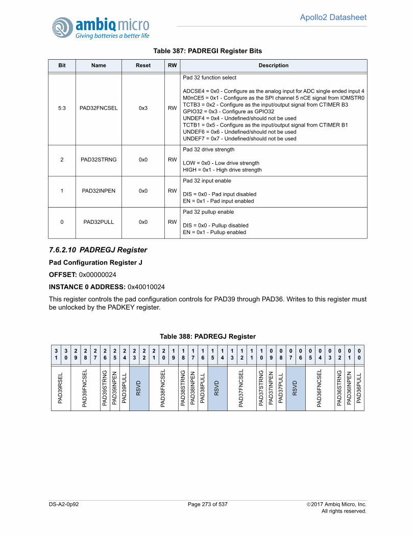
Apollo2 Datasheet
7.6.2.10 PADREGJ Register
Pad Configuration Register J
OFFSET: 0x00000024
INSTANCE 0 ADDRESS: 0x40010024
This register controls the pad configuration controls for PAD39 through PAD36. Writes to this register mustbe unlocked by the PADKEY register.
5:3 PAD32FNCSEL 0x3 RW
Pad 32 function select
ADCSE4 = 0x0 - Configure as the analog input for ADC single ended input 4M0nCE5 = 0x1 - Configure as the SPI channel 5 nCE signal from IOMSTR0TCTB3 = 0x2 - Configure as the input/output signal from CTIMER B3GPIO32 = 0x3 - Configure as GPIO32UNDEF4 = 0x4 - Undefined/should not be usedTCTB1 = 0x5 - Configure as the input/output signal from CTIMER B1UNDEF6 = 0x6 - Undefined/should not be usedUNDEF7 = 0x7 - Undefined/should not be used
2 PAD32STRNG 0x0 RW
Pad 32 drive strength
LOW = 0x0 - Low drive strengthHIGH = 0x1 - High drive strength
1 PAD32INPEN 0x0 RW
Pad 32 input enable
DIS = 0x0 - Pad input disabledEN = 0x1 - Pad input enabled
0 PAD32PULL 0x0 RW
Pad 32 pullup enable
DIS = 0x0 - Pullup disabledEN = 0x1 - Pullup enabled
Table 388: PADREGJ Register
31
30
29
28
27
26
25
24
23
22
21
20
19
18
17
16
15
14
13
12
11
10
09
08
07
06
05
04
03
02
01
00
PA
D39
RS
EL
PA
D39
FN
CS
EL
PA
D39
ST
RN
G
PA
D39
INP
EN
PA
D39
PU
LL
RS
VD
PA
D38
FN
CS
EL
PA
D38
ST
RN
G
PA
D38
INP
EN
PA
D38
PU
LL
RS
VD
PA
D37
FN
CS
EL
PA
D37
ST
RN
G
PA
D37
INP
EN
PA
D37
PU
LL
RS
VD
PA
D36
FN
CS
EL
PA
D36
ST
RN
G
PA
D36
INP
EN
PA
D36
PU
LL
Table 387: PADREGI Register Bits
Bit Name Reset RW Description
DS-A2-0p92 Page 273 of 537 2017 Ambiq Micro, Inc.All rights reserved.

Apollo2 Datasheet
Table 389: PADREGJ Register Bits
Bit Name Reset RW Description
31:30 PAD39RSEL 0x0 RW
Pad 39 pullup resistor selection.
PULL1_5K = 0x0 - Pullup is ~1.5 KOhmsPULL6K = 0x1 - Pullup is ~6 KOhmsPULL12K = 0x2 - Pullup is ~12 KOhmsPULL24K = 0x3 - Pullup is ~24 KOhms
29:27 PAD39FNCSEL 0x3 RW
Pad 39 function select
UART0TX = 0x0 - Configure as the UART0 TX SignalUART1TX = 0x1 - Configure as the UART1 TX signalCLKOUT = 0x2 - Configure as the CLKOUT signalGPIO39 = 0x3 - Configure as GPIO39M4SCL = 0x4 - Configure as the IOMSTR4 I2C SCL signalM4SCK = 0x5 - Configure as the IOMSTR4 SPI SCK signalM4SCKLB = 0x6 - Configure as the IOMSTR4 SPI SCK loopback signalfrom IOSLAVEM4SCLLB = 0x7 - Configure as the IOMSTR4 I2C SCL loopback signal fromIOSLAVE
26 PAD39STRNG 0x0 RW
Pad 39 drive strength
LOW = 0x0 - Low drive strengthHIGH = 0x1 - High drive strength
25 PAD39INPEN 0x0 RW
Pad 39 input enable
DIS = 0x0 - Pad input disabledEN = 0x1 - Pad input enabled
24 PAD39PULL 0x0 RW
Pad 39 pullup enable
DIS = 0x0 - Pullup disabledEN = 0x1 - Pullup enabled
23:22 RSVD 0x0 RORESERVED
21:19 PAD38FNCSEL 0x3 RW
Pad 38 function select
TRIG3 = 0x0 - Configure as the ADC Trigger 3 signalM1nCE3 = 0x1 - Configure as the SPI channel 3 nCE signal from IOMSTR1UA0CTS = 0x2 - Configure as the UART0 CTS signalGPIO38 = 0x3 - Configure as GPIO38M3WIR3 = 0x4 - Configure as the IOSLAVE SPI 3-wire MOSI/MISO signalM3MOSI = 0x5 - Configure as the IOMSTR3 SPI MOSI output signalM4nCE7 = 0x6 - Configure as the SPI channel 7 nCE signal from IOMSTR4SLWIR3LB = 0x7 - Configure as the IOMSTR3 SPI 3-wire MOSI/MISO loop-back signal from IOSLAVE
18 PAD38STRNG 0x0 RW
Pad 38 drive strength
LOW = 0x0 - Low drive strengthHIGH = 0x1 - High drive strength
DS-A2-0p92 Page 274 of 537 2017 Ambiq Micro, Inc.All rights reserved.
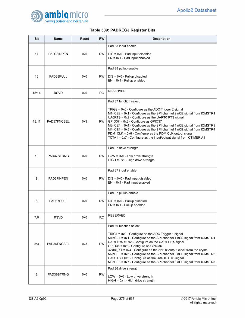
Apollo2 Datasheet
17 PAD38INPEN 0x0 RW
Pad 38 input enable
DIS = 0x0 - Pad input disabledEN = 0x1 - Pad input enabled
16 PAD38PULL 0x0 RW
Pad 38 pullup enable
DIS = 0x0 - Pullup disabledEN = 0x1 - Pullup enabled
15:14 RSVD 0x0 RORESERVED
13:11 PAD37FNCSEL 0x3 RW
Pad 37 function select
TRIG2 = 0x0 - Configure as the ADC Trigger 2 signalM1nCE2 = 0x1 - Configure as the SPI channel 2 nCE signal from IOMSTR1UA0RTS = 0x2 - Configure as the UART0 RTS signalGPIO37 = 0x3 - Configure as GPIO37M3nCE4 = 0x4 - Configure as the SPI channel 4 nCE signal from IOMSTR3M4nCE1 = 0x5 - Configure as the SPI channel 1 nCE signal from IOMSTR4PDM_CLK = 0x6 - Configure as the PDM CLK output signalTCTA1 = 0x7 - Configure as the input/output signal from CTIMER A1
10 PAD37STRNG 0x0 RW
Pad 37 drive strength
LOW = 0x0 - Low drive strengthHIGH = 0x1 - High drive strength
9 PAD37INPEN 0x0 RW
Pad 37 input enable
DIS = 0x0 - Pad input disabledEN = 0x1 - Pad input enabled
8 PAD37PULL 0x0 RW
Pad 37 pullup enable
DIS = 0x0 - Pullup disabledEN = 0x1 - Pullup enabled
7:6 RSVD 0x0 RORESERVED
5:3 PAD36FNCSEL 0x3 RW
Pad 36 function select
TRIG1 = 0x0 - Configure as the ADC Trigger 1 signalM1nCE1 = 0x1 - Configure as the SPI channel 1 nCE signal from IOMSTR1UART1RX = 0x2 - Configure as the UART1 RX signalGPIO36 = 0x3 - Configure as GPIO3632khz_XT = 0x4 - Configure as the 32kHz output clock from the crystalM2nCE0 = 0x5 - Configure as the SPI channel 0 nCE signal from IOMSTR2UA0CTS = 0x6 - Configure as the UART0 CTS signalM3nCE3 = 0x7 - Configure as the SPI channel 3 nCE signal from IOMSTR3
2 PAD36STRNG 0x0 RW
Pad 36 drive strength
LOW = 0x0 - Low drive strengthHIGH = 0x1 - High drive strength
Table 389: PADREGJ Register Bits
Bit Name Reset RW Description
DS-A2-0p92 Page 275 of 537 2017 Ambiq Micro, Inc.All rights reserved.
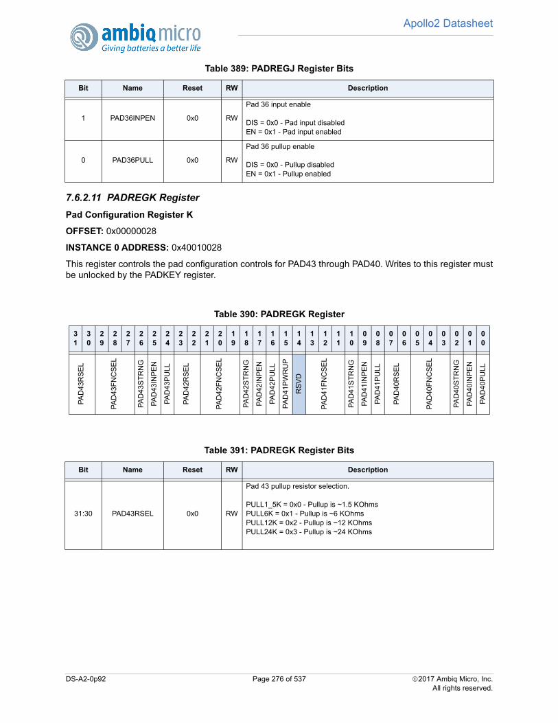
Apollo2 Datasheet
7.6.2.11 PADREGK Register
Pad Configuration Register K
OFFSET: 0x00000028
INSTANCE 0 ADDRESS: 0x40010028
This register controls the pad configuration controls for PAD43 through PAD40. Writes to this register mustbe unlocked by the PADKEY register.
1 PAD36INPEN 0x0 RW
Pad 36 input enable
DIS = 0x0 - Pad input disabledEN = 0x1 - Pad input enabled
0 PAD36PULL 0x0 RW
Pad 36 pullup enable
DIS = 0x0 - Pullup disabledEN = 0x1 - Pullup enabled
Table 390: PADREGK Register
31
30
29
28
27
26
25
24
23
22
21
20
19
18
17
16
15
14
13
12
11
10
09
08
07
06
05
04
03
02
01
00
PA
D43
RS
EL
PA
D43
FN
CS
EL
PA
D4
3ST
RN
G
PA
D43
INP
EN
PA
D43
PU
LL
PA
D42
RS
EL
PA
D42
FN
CS
EL
PA
D4
2ST
RN
G
PA
D42
INP
EN
PA
D42
PU
LL
PA
D41
PW
RU
P
RS
VD
PA
D41
FN
CS
EL
PA
D4
1ST
RN
G
PA
D41
INP
EN
PA
D41
PU
LL
PA
D40
RS
EL
PA
D40
FN
CS
EL
PA
D4
0ST
RN
G
PA
D40
INP
EN
PA
D40
PU
LL
Table 391: PADREGK Register Bits
Bit Name Reset RW Description
31:30 PAD43RSEL 0x0 RW
Pad 43 pullup resistor selection.
PULL1_5K = 0x0 - Pullup is ~1.5 KOhmsPULL6K = 0x1 - Pullup is ~6 KOhmsPULL12K = 0x2 - Pullup is ~12 KOhmsPULL24K = 0x3 - Pullup is ~24 KOhms
Table 389: PADREGJ Register Bits
Bit Name Reset RW Description
DS-A2-0p92 Page 276 of 537 2017 Ambiq Micro, Inc.All rights reserved.
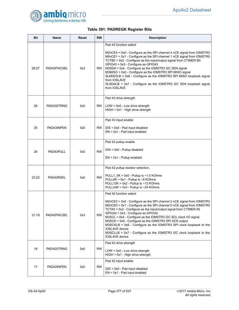
Apollo2 Datasheet
29:27 PAD43FNCSEL 0x3 RW
Pad 43 function select
M2nCE4 = 0x0 - Configure as the SPI channel 4 nCE signal from IOMSTR2M0nCE1 = 0x1 - Configure as the SPI channel 1 nCE signal from IOMSTR0TCTB0 = 0x2 - Configure as the input/output signal from CTIMER B0GPIO43 = 0x3 - Configure as GPIO43M3SDA = 0x4 - Configure as the IOMSTR3 I2C SDA signalM3MISO = 0x5 - Configure as the IOMSTR3 SPI MISO signalSLMISOLB = 0x6 - Configure as the IOMSTR3 SPI MISO loopback signalfrom IOSLAVESLSDALB = 0x7 - Configure as the IOMSTR3 I2C SDA loopback signalfrom IOSLAVE
26 PAD43STRNG 0x0 RW
Pad 43 drive strength
LOW = 0x0 - Low drive strengthHIGH = 0x1 - High drive strength
25 PAD43INPEN 0x0 RW
Pad 43 input enable
DIS = 0x0 - Pad input disabledEN = 0x1 - Pad input enabled
24 PAD43PULL 0x0 RW
Pad 43 pullup enable
DIS = 0x0 - Pullup disabled
EN = 0x1 - Pullup enabled
23:22 PAD42RSEL 0x0 RW
Pad 42 pullup resistor selection.
PULL1_5K = 0x0 - Pullup is ~1.5 KOhmsPULL6K = 0x1 - Pullup is ~6 KOhmsPULL12K = 0x2 - Pullup is ~12 KOhmsPULL24K = 0x3 - Pullup is ~24 KOhms
21:19 PAD42FNCSEL 0x3 RW
Pad 42 function select
M2nCE2 = 0x0 - Configure as the SPI channel 2 nCE signal from IOMSTR2M0nCE0 = 0x1 - Configure as the SPI channel 0 nCE signal from IOMSTR0TCTA0 = 0x2 - Configure as the input/output signal from CTIMER A0GPIO42 = 0x3 - Configure as GPIO42M3SCL = 0x4 - Configure as the IOMSTR3 I2C SCL clock I/O signalM3SCK = 0x5 - Configure as the IOMSTR3 SPI SCK outputM3SCKLB = 0x6 - Configure as the IOMSTR3 SPI clock loopback to theIOSLAVE deviceM3SCLLB = 0x7 - Configure as the IOMSTR3 I2C clock loopback to theIOSLAVE device
18 PAD42STRNG 0x0 RW
Pad 42 drive strength
LOW = 0x0 - Low drive strengthHIGH = 0x1 - High drive strength
17 PAD42INPEN 0x0 RW
Pad 42 input enable
DIS = 0x0 - Pad input disabledEN = 0x1 - Pad input enabled
Table 391: PADREGK Register Bits
Bit Name Reset RW Description
DS-A2-0p92 Page 277 of 537 2017 Ambiq Micro, Inc.All rights reserved.
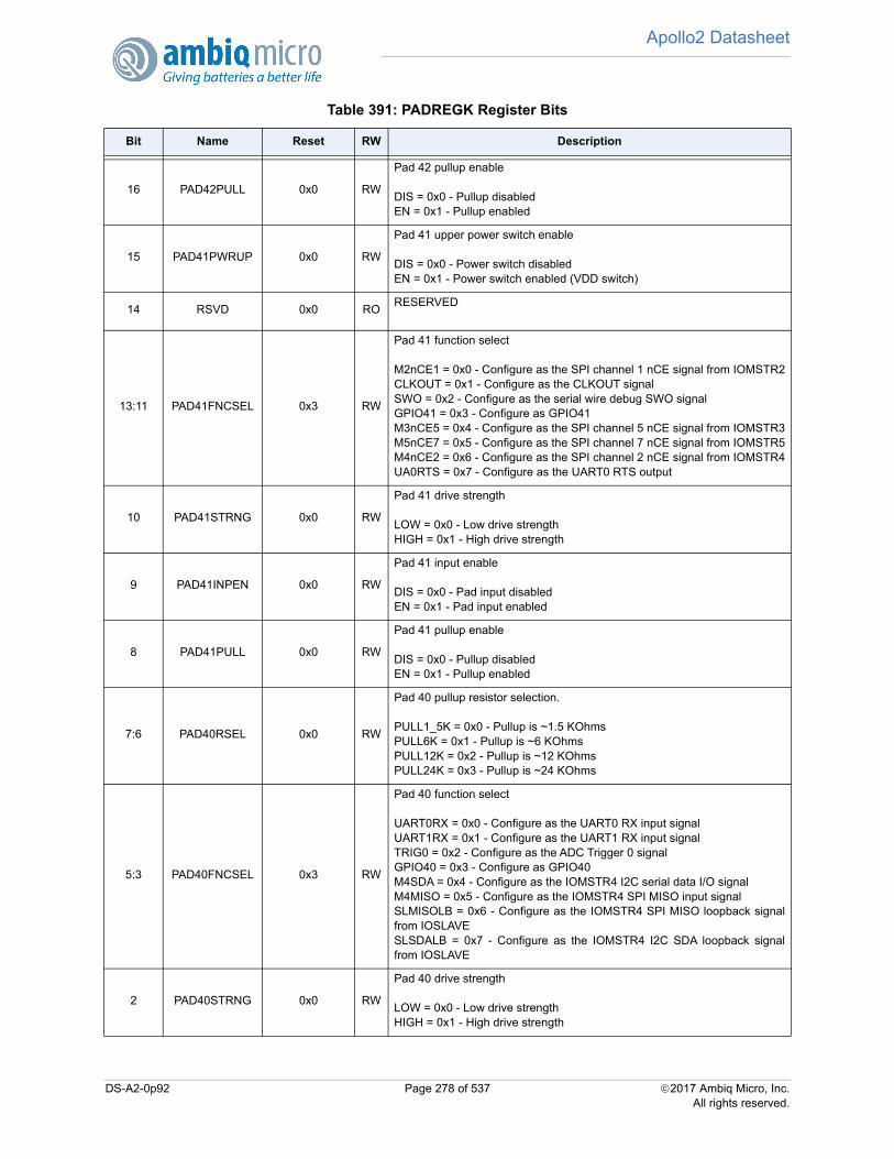
Apollo2 Datasheet
16 PAD42PULL 0x0 RW
Pad 42 pullup enable
DIS = 0x0 - Pullup disabledEN = 0x1 - Pullup enabled
15 PAD41PWRUP 0x0 RW
Pad 41 upper power switch enable
DIS = 0x0 - Power switch disabledEN = 0x1 - Power switch enabled (VDD switch)
14 RSVD 0x0 RORESERVED
13:11 PAD41FNCSEL 0x3 RW
Pad 41 function select
M2nCE1 = 0x0 - Configure as the SPI channel 1 nCE signal from IOMSTR2CLKOUT = 0x1 - Configure as the CLKOUT signalSWO = 0x2 - Configure as the serial wire debug SWO signalGPIO41 = 0x3 - Configure as GPIO41M3nCE5 = 0x4 - Configure as the SPI channel 5 nCE signal from IOMSTR3M5nCE7 = 0x5 - Configure as the SPI channel 7 nCE signal from IOMSTR5M4nCE2 = 0x6 - Configure as the SPI channel 2 nCE signal from IOMSTR4UA0RTS = 0x7 - Configure as the UART0 RTS output
10 PAD41STRNG 0x0 RW
Pad 41 drive strength
LOW = 0x0 - Low drive strengthHIGH = 0x1 - High drive strength
9 PAD41INPEN 0x0 RW
Pad 41 input enable
DIS = 0x0 - Pad input disabledEN = 0x1 - Pad input enabled
8 PAD41PULL 0x0 RW
Pad 41 pullup enable
DIS = 0x0 - Pullup disabledEN = 0x1 - Pullup enabled
7:6 PAD40RSEL 0x0 RW
Pad 40 pullup resistor selection.
PULL1_5K = 0x0 - Pullup is ~1.5 KOhmsPULL6K = 0x1 - Pullup is ~6 KOhmsPULL12K = 0x2 - Pullup is ~12 KOhmsPULL24K = 0x3 - Pullup is ~24 KOhms
5:3 PAD40FNCSEL 0x3 RW
Pad 40 function select
UART0RX = 0x0 - Configure as the UART0 RX input signalUART1RX = 0x1 - Configure as the UART1 RX input signalTRIG0 = 0x2 - Configure as the ADC Trigger 0 signalGPIO40 = 0x3 - Configure as GPIO40M4SDA = 0x4 - Configure as the IOMSTR4 I2C serial data I/O signalM4MISO = 0x5 - Configure as the IOMSTR4 SPI MISO input signalSLMISOLB = 0x6 - Configure as the IOMSTR4 SPI MISO loopback signalfrom IOSLAVESLSDALB = 0x7 - Configure as the IOMSTR4 I2C SDA loopback signalfrom IOSLAVE
2 PAD40STRNG 0x0 RW
Pad 40 drive strength
LOW = 0x0 - Low drive strengthHIGH = 0x1 - High drive strength
Table 391: PADREGK Register Bits
Bit Name Reset RW Description
DS-A2-0p92 Page 278 of 537 2017 Ambiq Micro, Inc.All rights reserved.
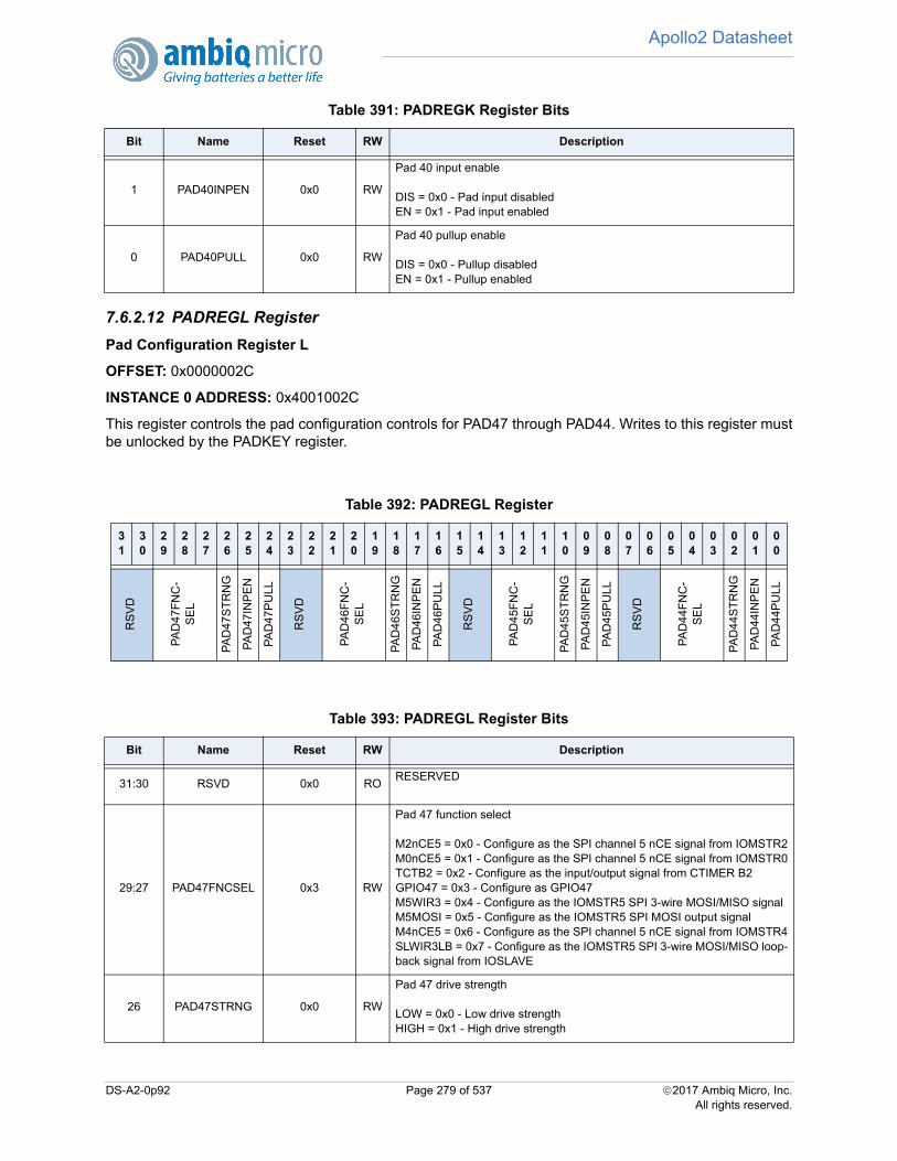
Apollo2 Datasheet
7.6.2.12 PADREGL Register
Pad Configuration Register L
OFFSET: 0x0000002C
INSTANCE 0 ADDRESS: 0x4001002C
This register controls the pad configuration controls for PAD47 through PAD44. Writes to this register mustbe unlocked by the PADKEY register.
1 PAD40INPEN 0x0 RW
Pad 40 input enable
DIS = 0x0 - Pad input disabledEN = 0x1 - Pad input enabled
0 PAD40PULL 0x0 RW
Pad 40 pullup enable
DIS = 0x0 - Pullup disabledEN = 0x1 - Pullup enabled
Table 392: PADREGL Register
31
30
29
28
27
26
25
24
23
22
21
20
19
18
17
16
15
14
13
12
11
10
09
08
07
06
05
04
03
02
01
00
RS
VD
PA
D47
FN
C-
SE
L
PA
D4
7ST
RN
G
PA
D47
INP
EN
PA
D47
PU
LL
RS
VD
PA
D46
FN
C-
SE
L
PA
D4
6ST
RN
G
PA
D46
INP
EN
PA
D46
PU
LL
RS
VD
PA
D45
FN
C-
SE
L
PA
D4
5ST
RN
G
PA
D45
INP
EN
PA
D45
PU
LL
RS
VD
PA
D44
FN
C-
SE
L
PA
D4
4ST
RN
G
PA
D44
INP
EN
PA
D44
PU
LL
Table 393: PADREGL Register Bits
Bit Name Reset RW Description
31:30 RSVD 0x0 RORESERVED
29:27 PAD47FNCSEL 0x3 RW
Pad 47 function select
M2nCE5 = 0x0 - Configure as the SPI channel 5 nCE signal from IOMSTR2M0nCE5 = 0x1 - Configure as the SPI channel 5 nCE signal from IOMSTR0TCTB2 = 0x2 - Configure as the input/output signal from CTIMER B2GPIO47 = 0x3 - Configure as GPIO47M5WIR3 = 0x4 - Configure as the IOMSTR5 SPI 3-wire MOSI/MISO signalM5MOSI = 0x5 - Configure as the IOMSTR5 SPI MOSI output signalM4nCE5 = 0x6 - Configure as the SPI channel 5 nCE signal from IOMSTR4SLWIR3LB = 0x7 - Configure as the IOMSTR5 SPI 3-wire MOSI/MISO loop-back signal from IOSLAVE
26 PAD47STRNG 0x0 RW
Pad 47 drive strength
LOW = 0x0 - Low drive strengthHIGH = 0x1 - High drive strength
Table 391: PADREGK Register Bits
Bit Name Reset RW Description
DS-A2-0p92 Page 279 of 537 2017 Ambiq Micro, Inc.All rights reserved.

Apollo2 Datasheet
25 PAD47INPEN 0x0 RW
Pad 47 input enable
DIS = 0x0 - Pad input disabledEN = 0x1 - Pad input enabled
24 PAD47PULL 0x0 RW
Pad 47 pullup enable
DIS = 0x0 - Pullup disabledEN = 0x1 - Pullup enabled
23:22 RSVD 0x0 RORESERVED
21:19 PAD46FNCSEL 0x3 RW
Pad 46 function select
32khz_XT = 0x0 - Configure as the 32kHz output clock from the crystalM0nCE4 = 0x1 - Configure as the SPI channel 4 nCE signal from IOMSTR0TCTA2 = 0x2 - Configure as the input/output signal from CTIMER A2GPIO46 = 0x3 - Configure as GPIO46TCTA1 = 0x4 - Configure as the input/output signal from CTIMER A1M5nCE4 = 0x5 - Configure as the SPI channel 4 nCE signal from IOMSTR5M4nCE4 = 0x6 - Configure as the SPI channel 4 nCE signal from IOMSTR4SWO = 0x7 - Configure as the serial wire debug SWO signal
18 PAD46STRNG 0x0 RW
Pad 46 drive strength
LOW = 0x0 - Low drive strengthHIGH = 0x1 - High drive strength
17 PAD46INPEN 0x0 RW
Pad 46 input enable
DIS = 0x0 - Pad input disabledEN = 0x1 - Pad input enabled
16 PAD46PULL 0x0 RW
Pad 46 pullup enable
DIS = 0x0 - Pullup disabledEN = 0x1 - Pullup enabled
15:14 RSVD 0x0 RORESERVED
13:11 PAD45FNCSEL 0x3 RW
Pad 45 function select
UA1CTS = 0x0 - Configure as the UART1 CTS input signalM0nCE3 = 0x1 - Configure as the SPI channel 3 nCE signal from IOMSTR0TCTB1 = 0x2 - Configure as the input/output signal from CTIMER B1GPIO45 = 0x3 - Configure as GPIO45M4nCE3 = 0x4 - Configure as the SPI channel 3 nCE signal from IOMSTR4M3nCE6 = 0x5 - Configure as the SPI channel 6 nCE signal from IOMSTR3M5nCE5 = 0x6 - Configure as the SPI channel 5 nCE signal from IOMSTR5TCTA1 = 0x7 - Configure as the input/output signal from CTIMER A1
10 PAD45STRNG 0x0 RW
Pad 45 drive strength
LOW = 0x0 - Low drive strengthHIGH = 0x1 - High drive strength
9 PAD45INPEN 0x0 RW
Pad 45 input enable
DIS = 0x0 - Pad input disabledEN = 0x1 - Pad input enabled
Table 393: PADREGL Register Bits
Bit Name Reset RW Description
DS-A2-0p92 Page 280 of 537 2017 Ambiq Micro, Inc.All rights reserved.
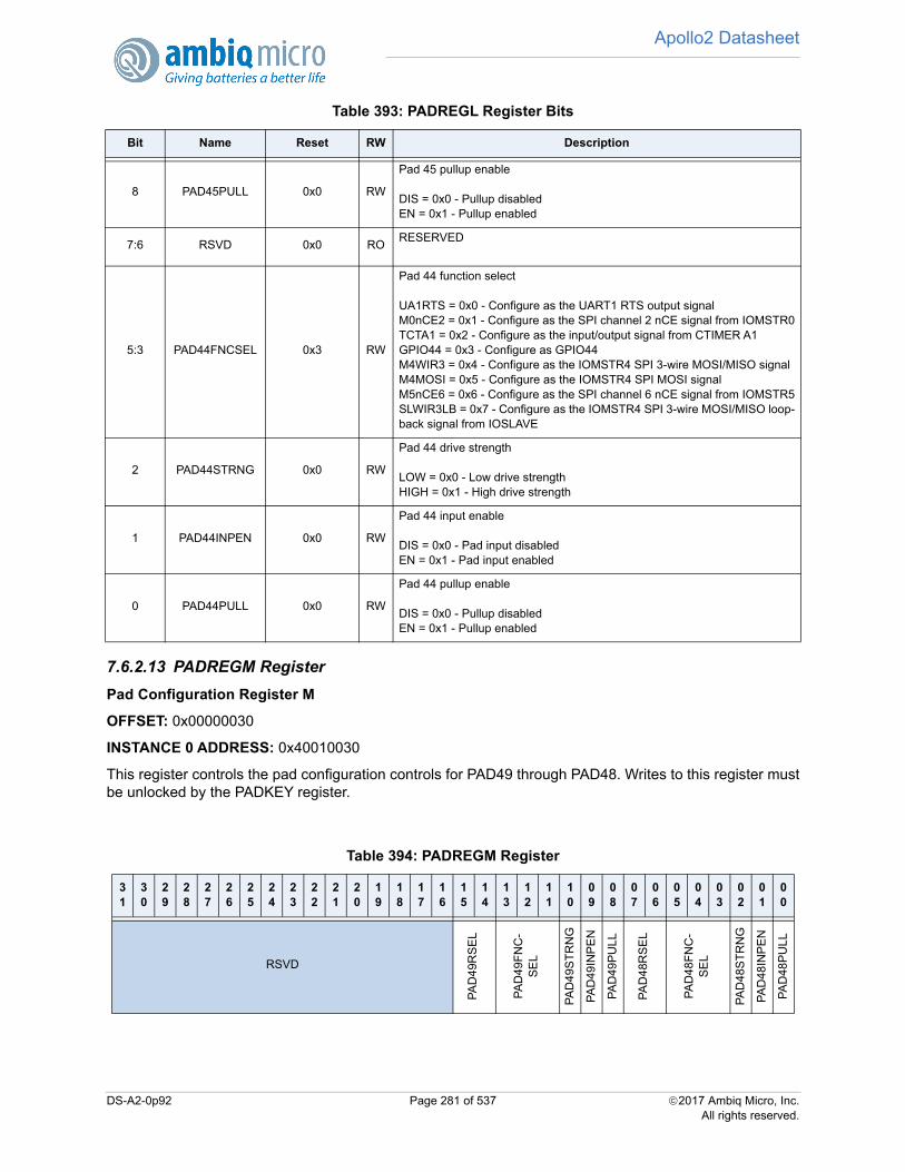
Apollo2 Datasheet
7.6.2.13 PADREGM Register
Pad Configuration Register M
OFFSET: 0x00000030
INSTANCE 0 ADDRESS: 0x40010030
This register controls the pad configuration controls for PAD49 through PAD48. Writes to this register mustbe unlocked by the PADKEY register.
8 PAD45PULL 0x0 RW
Pad 45 pullup enable
DIS = 0x0 - Pullup disabledEN = 0x1 - Pullup enabled
7:6 RSVD 0x0 RORESERVED
5:3 PAD44FNCSEL 0x3 RW
Pad 44 function select
UA1RTS = 0x0 - Configure as the UART1 RTS output signalM0nCE2 = 0x1 - Configure as the SPI channel 2 nCE signal from IOMSTR0TCTA1 = 0x2 - Configure as the input/output signal from CTIMER A1GPIO44 = 0x3 - Configure as GPIO44M4WIR3 = 0x4 - Configure as the IOMSTR4 SPI 3-wire MOSI/MISO signalM4MOSI = 0x5 - Configure as the IOMSTR4 SPI MOSI signalM5nCE6 = 0x6 - Configure as the SPI channel 6 nCE signal from IOMSTR5SLWIR3LB = 0x7 - Configure as the IOMSTR4 SPI 3-wire MOSI/MISO loop-back signal from IOSLAVE
2 PAD44STRNG 0x0 RW
Pad 44 drive strength
LOW = 0x0 - Low drive strengthHIGH = 0x1 - High drive strength
1 PAD44INPEN 0x0 RW
Pad 44 input enable
DIS = 0x0 - Pad input disabledEN = 0x1 - Pad input enabled
0 PAD44PULL 0x0 RW
Pad 44 pullup enable
DIS = 0x0 - Pullup disabledEN = 0x1 - Pullup enabled
Table 394: PADREGM Register
31
30
29
28
27
26
25
24
23
22
21
20
19
18
17
16
15
14
13
12
11
10
09
08
07
06
05
04
03
02
01
00
RSVD
PA
D4
9RS
EL
PA
D49
FN
C-
SE
L
PA
D49
ST
RN
G
PA
D49
INP
EN
PA
D49
PU
LL
PA
D4
8RS
EL
PA
D48
FN
C-
SE
L
PA
D48
ST
RN
G
PA
D48
INP
EN
PA
D48
PU
LL
Table 393: PADREGL Register Bits
Bit Name Reset RW Description
DS-A2-0p92 Page 281 of 537 2017 Ambiq Micro, Inc.All rights reserved.
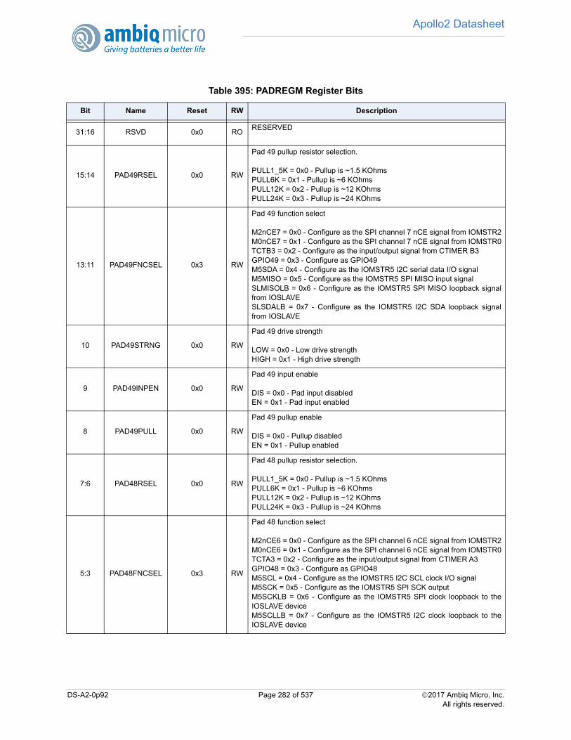
Apollo2 Datasheet
Table 395: PADREGM Register Bits
Bit Name Reset RW Description
31:16 RSVD 0x0 RORESERVED
15:14 PAD49RSEL 0x0 RW
Pad 49 pullup resistor selection.
PULL1_5K = 0x0 - Pullup is ~1.5 KOhmsPULL6K = 0x1 - Pullup is ~6 KOhmsPULL12K = 0x2 - Pullup is ~12 KOhmsPULL24K = 0x3 - Pullup is ~24 KOhms
13:11 PAD49FNCSEL 0x3 RW
Pad 49 function select
M2nCE7 = 0x0 - Configure as the SPI channel 7 nCE signal from IOMSTR2M0nCE7 = 0x1 - Configure as the SPI channel 7 nCE signal from IOMSTR0TCTB3 = 0x2 - Configure as the input/output signal from CTIMER B3GPIO49 = 0x3 - Configure as GPIO49M5SDA = 0x4 - Configure as the IOMSTR5 I2C serial data I/O signalM5MISO = 0x5 - Configure as the IOMSTR5 SPI MISO input signalSLMISOLB = 0x6 - Configure as the IOMSTR5 SPI MISO loopback signalfrom IOSLAVESLSDALB = 0x7 - Configure as the IOMSTR5 I2C SDA loopback signalfrom IOSLAVE
10 PAD49STRNG 0x0 RW
Pad 49 drive strength
LOW = 0x0 - Low drive strengthHIGH = 0x1 - High drive strength
9 PAD49INPEN 0x0 RW
Pad 49 input enable
DIS = 0x0 - Pad input disabledEN = 0x1 - Pad input enabled
8 PAD49PULL 0x0 RW
Pad 49 pullup enable
DIS = 0x0 - Pullup disabledEN = 0x1 - Pullup enabled
7:6 PAD48RSEL 0x0 RW
Pad 48 pullup resistor selection.
PULL1_5K = 0x0 - Pullup is ~1.5 KOhmsPULL6K = 0x1 - Pullup is ~6 KOhmsPULL12K = 0x2 - Pullup is ~12 KOhmsPULL24K = 0x3 - Pullup is ~24 KOhms
5:3 PAD48FNCSEL 0x3 RW
Pad 48 function select
M2nCE6 = 0x0 - Configure as the SPI channel 6 nCE signal from IOMSTR2M0nCE6 = 0x1 - Configure as the SPI channel 6 nCE signal from IOMSTR0TCTA3 = 0x2 - Configure as the input/output signal from CTIMER A3GPIO48 = 0x3 - Configure as GPIO48M5SCL = 0x4 - Configure as the IOMSTR5 I2C SCL clock I/O signalM5SCK = 0x5 - Configure as the IOMSTR5 SPI SCK outputM5SCKLB = 0x6 - Configure as the IOMSTR5 SPI clock loopback to theIOSLAVE deviceM5SCLLB = 0x7 - Configure as the IOMSTR5 I2C clock loopback to theIOSLAVE device
DS-A2-0p92 Page 282 of 537 2017 Ambiq Micro, Inc.All rights reserved.
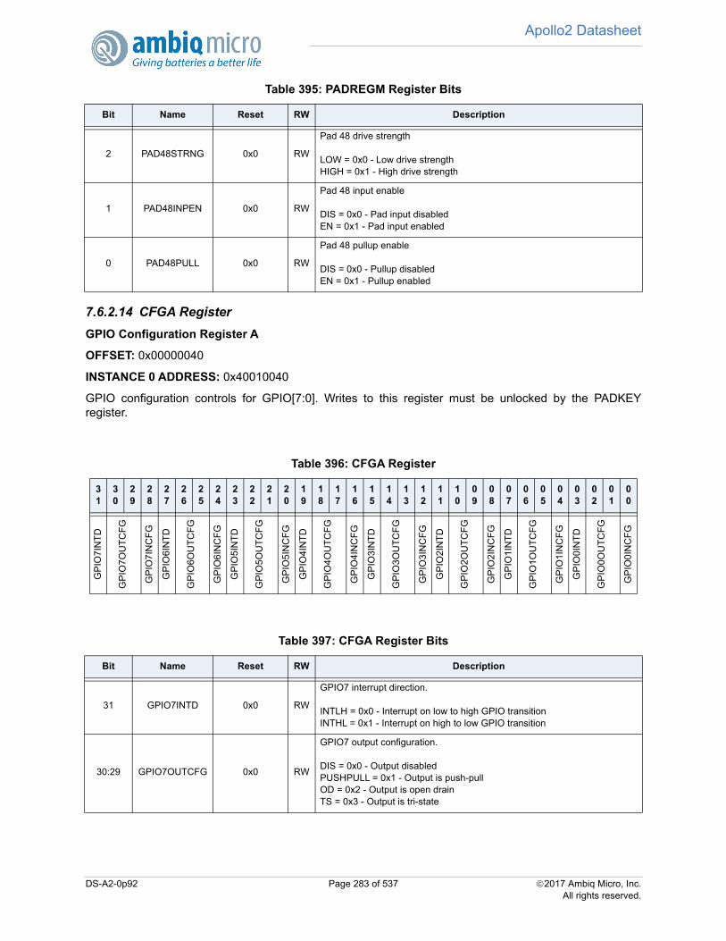
Apollo2 Datasheet
7.6.2.14 CFGA Register
GPIO Configuration Register A
OFFSET: 0x00000040
INSTANCE 0 ADDRESS: 0x40010040
GPIO configuration controls for GPIO[7:0]. Writes to this register must be unlocked by the PADKEYregister.
2 PAD48STRNG 0x0 RW
Pad 48 drive strength
LOW = 0x0 - Low drive strengthHIGH = 0x1 - High drive strength
1 PAD48INPEN 0x0 RW
Pad 48 input enable
DIS = 0x0 - Pad input disabledEN = 0x1 - Pad input enabled
0 PAD48PULL 0x0 RW
Pad 48 pullup enable
DIS = 0x0 - Pullup disabledEN = 0x1 - Pullup enabled
Table 396: CFGA Register
31
30
29
28
27
26
25
24
23
22
21
20
19
18
17
16
15
14
13
12
11
10
09
08
07
06
05
04
03
02
01
00
GP
IO7I
NT
D
GP
IO7O
UT
CF
G
GP
IO7I
NC
FG
GP
IO6I
NT
D
GP
IO6O
UT
CF
G
GP
IO6I
NC
FG
GP
IO5I
NT
D
GP
IO5O
UT
CF
G
GP
IO5I
NC
FG
GP
IO4I
NT
D
GP
IO4O
UT
CF
G
GP
IO4I
NC
FG
GP
IO3I
NT
D
GP
IO3O
UT
CF
G
GP
IO3I
NC
FG
GP
IO2I
NT
D
GP
IO2O
UT
CF
G
GP
IO2I
NC
FG
GP
IO1I
NT
D
GP
IO1O
UT
CF
G
GP
IO1I
NC
FG
GP
IO0I
NT
D
GP
IO0O
UT
CF
G
GP
IO0I
NC
FG
Table 397: CFGA Register Bits
Bit Name Reset RW Description
31 GPIO7INTD 0x0 RW
GPIO7 interrupt direction.
INTLH = 0x0 - Interrupt on low to high GPIO transitionINTHL = 0x1 - Interrupt on high to low GPIO transition
30:29 GPIO7OUTCFG 0x0 RW
GPIO7 output configuration.
DIS = 0x0 - Output disabledPUSHPULL = 0x1 - Output is push-pullOD = 0x2 - Output is open drainTS = 0x3 - Output is tri-state
Table 395: PADREGM Register Bits
Bit Name Reset RW Description
DS-A2-0p92 Page 283 of 537 2017 Ambiq Micro, Inc.All rights reserved.
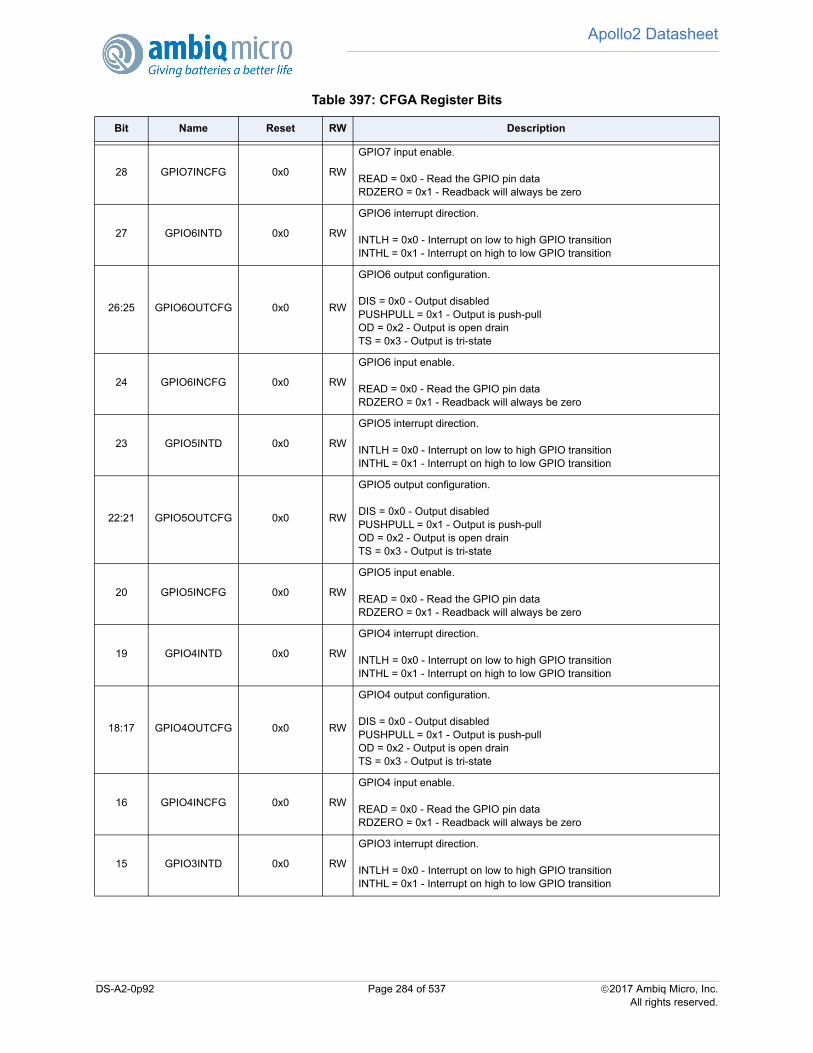
Apollo2 Datasheet
28 GPIO7INCFG 0x0 RW
GPIO7 input enable.
READ = 0x0 - Read the GPIO pin dataRDZERO = 0x1 - Readback will always be zero
27 GPIO6INTD 0x0 RW
GPIO6 interrupt direction.
INTLH = 0x0 - Interrupt on low to high GPIO transitionINTHL = 0x1 - Interrupt on high to low GPIO transition
26:25 GPIO6OUTCFG 0x0 RW
GPIO6 output configuration.
DIS = 0x0 - Output disabledPUSHPULL = 0x1 - Output is push-pullOD = 0x2 - Output is open drainTS = 0x3 - Output is tri-state
24 GPIO6INCFG 0x0 RW
GPIO6 input enable.
READ = 0x0 - Read the GPIO pin dataRDZERO = 0x1 - Readback will always be zero
23 GPIO5INTD 0x0 RW
GPIO5 interrupt direction.
INTLH = 0x0 - Interrupt on low to high GPIO transitionINTHL = 0x1 - Interrupt on high to low GPIO transition
22:21 GPIO5OUTCFG 0x0 RW
GPIO5 output configuration.
DIS = 0x0 - Output disabledPUSHPULL = 0x1 - Output is push-pullOD = 0x2 - Output is open drainTS = 0x3 - Output is tri-state
20 GPIO5INCFG 0x0 RW
GPIO5 input enable.
READ = 0x0 - Read the GPIO pin dataRDZERO = 0x1 - Readback will always be zero
19 GPIO4INTD 0x0 RW
GPIO4 interrupt direction.
INTLH = 0x0 - Interrupt on low to high GPIO transitionINTHL = 0x1 - Interrupt on high to low GPIO transition
18:17 GPIO4OUTCFG 0x0 RW
GPIO4 output configuration.
DIS = 0x0 - Output disabledPUSHPULL = 0x1 - Output is push-pullOD = 0x2 - Output is open drainTS = 0x3 - Output is tri-state
16 GPIO4INCFG 0x0 RW
GPIO4 input enable.
READ = 0x0 - Read the GPIO pin dataRDZERO = 0x1 - Readback will always be zero
15 GPIO3INTD 0x0 RW
GPIO3 interrupt direction.
INTLH = 0x0 - Interrupt on low to high GPIO transitionINTHL = 0x1 - Interrupt on high to low GPIO transition
Table 397: CFGA Register Bits
Bit Name Reset RW Description
DS-A2-0p92 Page 284 of 537 2017 Ambiq Micro, Inc.All rights reserved.
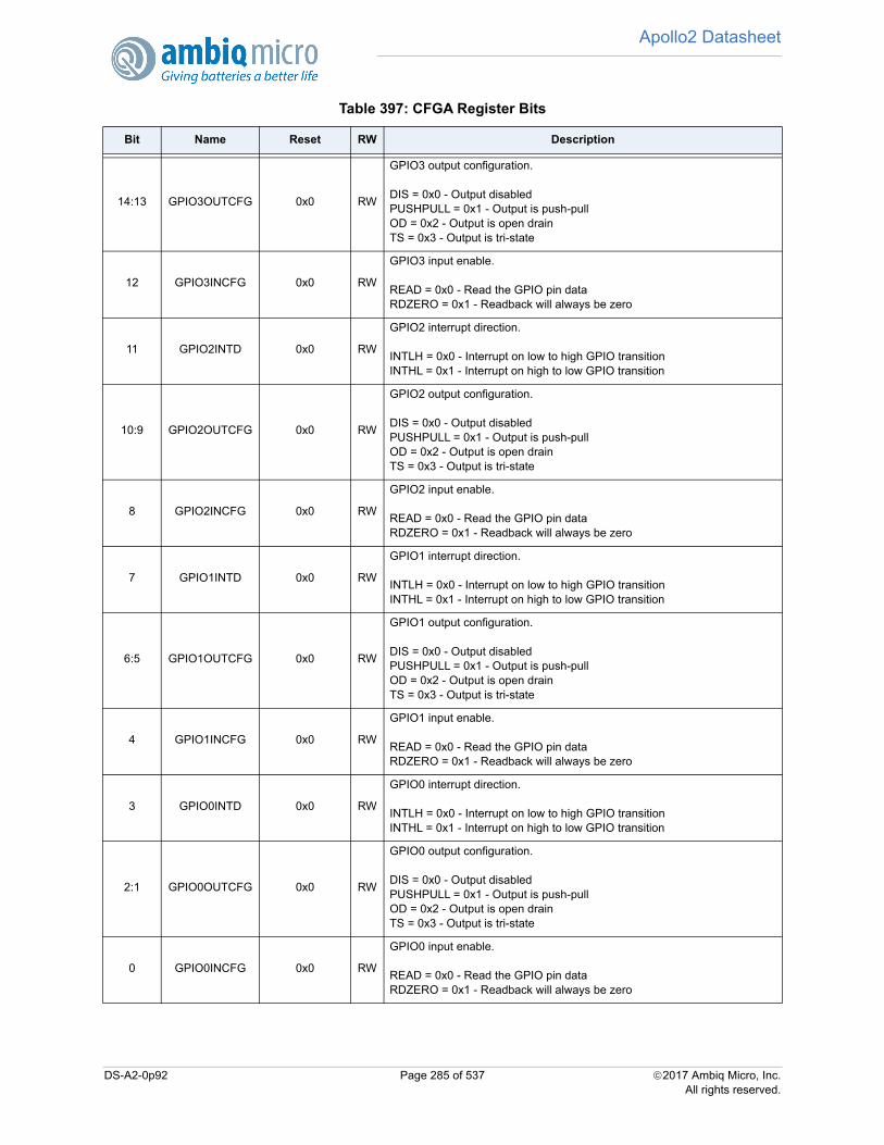
Apollo2 Datasheet
14:13 GPIO3OUTCFG 0x0 RW
GPIO3 output configuration.
DIS = 0x0 - Output disabledPUSHPULL = 0x1 - Output is push-pullOD = 0x2 - Output is open drainTS = 0x3 - Output is tri-state
12 GPIO3INCFG 0x0 RW
GPIO3 input enable.
READ = 0x0 - Read the GPIO pin dataRDZERO = 0x1 - Readback will always be zero
11 GPIO2INTD 0x0 RW
GPIO2 interrupt direction.
INTLH = 0x0 - Interrupt on low to high GPIO transitionINTHL = 0x1 - Interrupt on high to low GPIO transition
10:9 GPIO2OUTCFG 0x0 RW
GPIO2 output configuration.
DIS = 0x0 - Output disabledPUSHPULL = 0x1 - Output is push-pullOD = 0x2 - Output is open drainTS = 0x3 - Output is tri-state
8 GPIO2INCFG 0x0 RW
GPIO2 input enable.
READ = 0x0 - Read the GPIO pin dataRDZERO = 0x1 - Readback will always be zero
7 GPIO1INTD 0x0 RW
GPIO1 interrupt direction.
INTLH = 0x0 - Interrupt on low to high GPIO transitionINTHL = 0x1 - Interrupt on high to low GPIO transition
6:5 GPIO1OUTCFG 0x0 RW
GPIO1 output configuration.
DIS = 0x0 - Output disabledPUSHPULL = 0x1 - Output is push-pullOD = 0x2 - Output is open drainTS = 0x3 - Output is tri-state
4 GPIO1INCFG 0x0 RW
GPIO1 input enable.
READ = 0x0 - Read the GPIO pin dataRDZERO = 0x1 - Readback will always be zero
3 GPIO0INTD 0x0 RW
GPIO0 interrupt direction.
INTLH = 0x0 - Interrupt on low to high GPIO transitionINTHL = 0x1 - Interrupt on high to low GPIO transition
2:1 GPIO0OUTCFG 0x0 RW
GPIO0 output configuration.
DIS = 0x0 - Output disabledPUSHPULL = 0x1 - Output is push-pullOD = 0x2 - Output is open drainTS = 0x3 - Output is tri-state
0 GPIO0INCFG 0x0 RW
GPIO0 input enable.
READ = 0x0 - Read the GPIO pin dataRDZERO = 0x1 - Readback will always be zero
Table 397: CFGA Register Bits
Bit Name Reset RW Description
DS-A2-0p92 Page 285 of 537 2017 Ambiq Micro, Inc.All rights reserved.
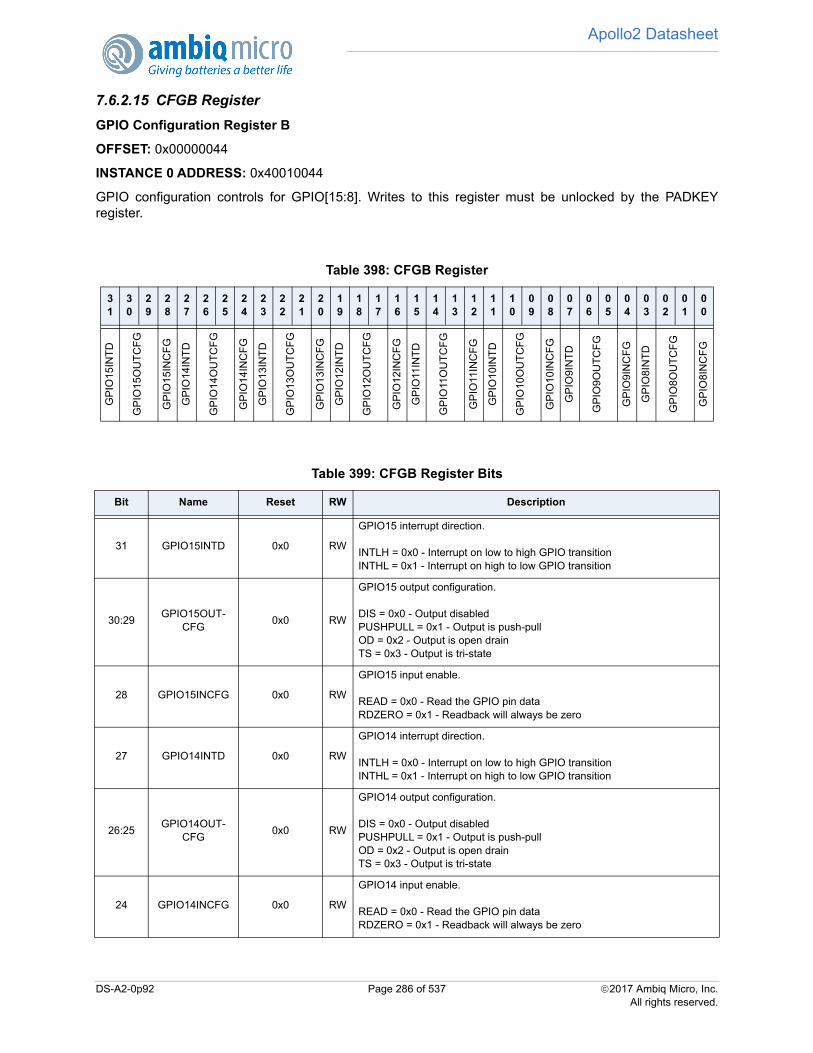
Apollo2 Datasheet
7.6.2.15 CFGB Register
GPIO Configuration Register B
OFFSET: 0x00000044
INSTANCE 0 ADDRESS: 0x40010044
GPIO configuration controls for GPIO[15:8]. Writes to this register must be unlocked by the PADKEYregister.
Table 398: CFGB Register
31
30
29
28
27
26
25
24
23
22
21
20
19
18
17
16
15
14
13
12
11
10
09
08
07
06
05
04
03
02
01
00
GP
IO15
INT
D
GP
IO15
OU
TC
FG
GP
IO15
INC
FG
GP
IO14
INT
D
GP
IO14
OU
TC
FG
GP
IO14
INC
FG
GP
IO13
INT
D
GP
IO13
OU
TC
FG
GP
IO13
INC
FG
GP
IO12
INT
D
GP
IO12
OU
TC
FG
GP
IO12
INC
FG
GP
IO11
INT
D
GP
IO11
OU
TC
FG
GP
IO11
INC
FG
GP
IO10
INT
D
GP
IO10
OU
TC
FG
GP
IO10
INC
FG
GP
IO9I
NT
D
GP
IO9
OU
TC
FG
GP
IO9I
NC
FG
GP
IO8I
NT
D
GP
IO8
OU
TC
FG
GP
IO8I
NC
FG
Table 399: CFGB Register Bits
Bit Name Reset RW Description
31 GPIO15INTD 0x0 RW
GPIO15 interrupt direction.
INTLH = 0x0 - Interrupt on low to high GPIO transitionINTHL = 0x1 - Interrupt on high to low GPIO transition
30:29GPIO15OUT-
CFG0x0 RW
GPIO15 output configuration.
DIS = 0x0 - Output disabledPUSHPULL = 0x1 - Output is push-pullOD = 0x2 - Output is open drainTS = 0x3 - Output is tri-state
28 GPIO15INCFG 0x0 RW
GPIO15 input enable.
READ = 0x0 - Read the GPIO pin dataRDZERO = 0x1 - Readback will always be zero
27 GPIO14INTD 0x0 RW
GPIO14 interrupt direction.
INTLH = 0x0 - Interrupt on low to high GPIO transitionINTHL = 0x1 - Interrupt on high to low GPIO transition
26:25GPIO14OUT-
CFG0x0 RW
GPIO14 output configuration.
DIS = 0x0 - Output disabledPUSHPULL = 0x1 - Output is push-pullOD = 0x2 - Output is open drainTS = 0x3 - Output is tri-state
24 GPIO14INCFG 0x0 RW
GPIO14 input enable.
READ = 0x0 - Read the GPIO pin dataRDZERO = 0x1 - Readback will always be zero
DS-A2-0p92 Page 286 of 537 2017 Ambiq Micro, Inc.All rights reserved.

Apollo2 Datasheet
23 GPIO13INTD 0x0 RW
GPIO13 interrupt direction.
INTLH = 0x0 - Interrupt on low to high GPIO transitionINTHL = 0x1 - Interrupt on high to low GPIO transition
22:21GPIO13OUT-
CFG0x0 RW
GPIO13 output configuration.
DIS = 0x0 - Output disabledPUSHPULL = 0x1 - Output is push-pullOD = 0x2 - Output is open drainTS = 0x3 - Output is tri-state
20 GPIO13INCFG 0x0 RW
GPIO13 input enable.
READ = 0x0 - Read the GPIO pin dataRDZERO = 0x1 - Readback will always be zero
19 GPIO12INTD 0x0 RW
GPIO12 interrupt direction.
INTLH = 0x0 - Interrupt on low to high GPIO transitionINTHL = 0x1 - Interrupt on high to low GPIO transition
18:17GPIO12OUT-
CFG0x0 RW
GPIO12 output configuration.
DIS = 0x0 - Output disabledPUSHPULL = 0x1 - Output is push-pullOD = 0x2 - Output is open drainTS = 0x3 - Output is tri-state
16 GPIO12INCFG 0x0 RW
GPIO12 input enable.
READ = 0x0 - Read the GPIO pin dataRDZERO = 0x1 - Readback will always be zero
15 GPIO11INTD 0x0 RW
GPIO11 interrupt direction.
INTLH = 0x0 - Interrupt on low to high GPIO transitionINTHL = 0x1 - Interrupt on high to low GPIO transition
14:13GPIO11OUT-
CFG0x0 RW
GPIO11 output configuration.
DIS = 0x0 - Output disabledPUSHPULL = 0x1 - Output is push-pullOD = 0x2 - Output is open drainTS = 0x3 - Output is tri-state
12 GPIO11INCFG 0x0 RW
GPIO11 input enable.
READ = 0x0 - Read the GPIO pin dataRDZERO = 0x1 - Readback will always be zero
11 GPIO10INTD 0x0 RW
GPIO10 interrupt direction.
INTLH = 0x0 - Interrupt on low to high GPIO transitionINTHL = 0x1 - Interrupt on high to low GPIO transition
10:9GPIO10OUT-
CFG0x0 RW
GPIO10 output configuration.
DIS = 0x0 - Output disabledPUSHPULL = 0x1 - Output is push-pullOD = 0x2 - Output is open drainTS = 0x3 - Output is tri-state
Table 399: CFGB Register Bits
Bit Name Reset RW Description
DS-A2-0p92 Page 287 of 537 2017 Ambiq Micro, Inc.All rights reserved.
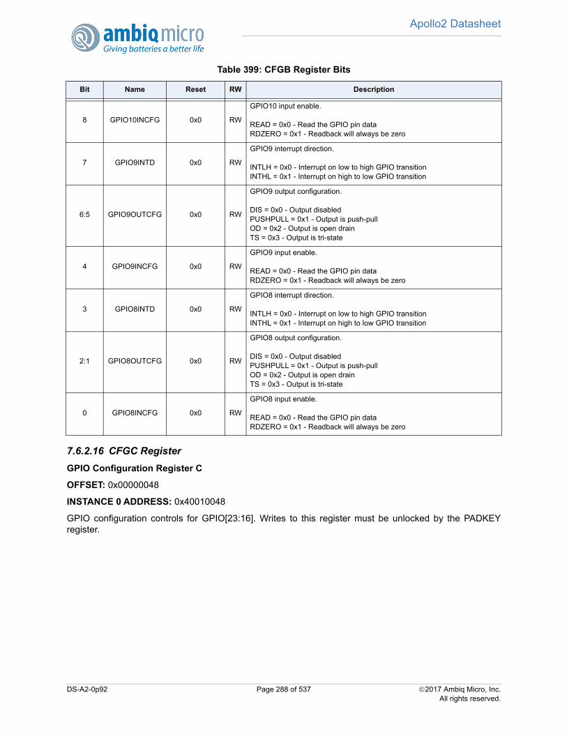
Apollo2 Datasheet
7.6.2.16 CFGC Register
GPIO Configuration Register C
OFFSET: 0x00000048
INSTANCE 0 ADDRESS: 0x40010048
GPIO configuration controls for GPIO[23:16]. Writes to this register must be unlocked by the PADKEYregister.
8 GPIO10INCFG 0x0 RW
GPIO10 input enable.
READ = 0x0 - Read the GPIO pin dataRDZERO = 0x1 - Readback will always be zero
7 GPIO9INTD 0x0 RW
GPIO9 interrupt direction.
INTLH = 0x0 - Interrupt on low to high GPIO transitionINTHL = 0x1 - Interrupt on high to low GPIO transition
6:5 GPIO9OUTCFG 0x0 RW
GPIO9 output configuration.
DIS = 0x0 - Output disabledPUSHPULL = 0x1 - Output is push-pullOD = 0x2 - Output is open drainTS = 0x3 - Output is tri-state
4 GPIO9INCFG 0x0 RW
GPIO9 input enable.
READ = 0x0 - Read the GPIO pin dataRDZERO = 0x1 - Readback will always be zero
3 GPIO8INTD 0x0 RW
GPIO8 interrupt direction.
INTLH = 0x0 - Interrupt on low to high GPIO transitionINTHL = 0x1 - Interrupt on high to low GPIO transition
2:1 GPIO8OUTCFG 0x0 RW
GPIO8 output configuration.
DIS = 0x0 - Output disabledPUSHPULL = 0x1 - Output is push-pullOD = 0x2 - Output is open drainTS = 0x3 - Output is tri-state
0 GPIO8INCFG 0x0 RW
GPIO8 input enable.
READ = 0x0 - Read the GPIO pin dataRDZERO = 0x1 - Readback will always be zero
Table 399: CFGB Register Bits
Bit Name Reset RW Description
DS-A2-0p92 Page 288 of 537 2017 Ambiq Micro, Inc.All rights reserved.
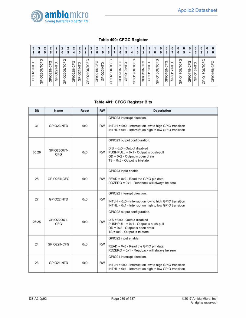
Apollo2 Datasheet
Table 400: CFGC Register
31
30
29
28
27
26
25
24
23
22
21
20
19
18
17
16
15
14
13
12
11
10
09
08
07
06
05
04
03
02
01
00
GP
IO23
INT
D
GP
IO23
OU
TC
FG
GP
IO2
3IN
CF
G
GP
IO22
INT
D
GP
IO22
OU
TC
FG
GP
IO2
2IN
CF
G
GP
IO21
INT
D
GP
IO21
OU
TC
FG
GP
IO2
1IN
CF
G
GP
IO20
INT
D
GP
IO20
OU
TC
FG
GP
IO2
0IN
CF
G
GP
IO19
INT
D
GP
IO19
OU
TC
FG
GP
IO1
9IN
CF
G
GP
IO18
INT
D
GP
IO18
OU
TC
FG
GP
IO1
8IN
CF
G
GP
IO17
INT
D
GP
IO17
OU
TC
FG
GP
IO1
7IN
CF
G
GP
IO16
INT
D
GP
IO16
OU
TC
FG
GP
IO1
6IN
CF
G
Table 401: CFGC Register Bits
Bit Name Reset RW Description
31 GPIO23INTD 0x0 RW
GPIO23 interrupt direction.
INTLH = 0x0 - Interrupt on low to high GPIO transitionINTHL = 0x1 - Interrupt on high to low GPIO transition
30:29GPIO23OUT-
CFG 0x0 RW
GPIO23 output configuration.
DIS = 0x0 - Output disabledPUSHPULL = 0x1 - Output is push-pullOD = 0x2 - Output is open drainTS = 0x3 - Output is tri-state
28 GPIO23INCFG 0x0 RW
GPIO23 input enable.
READ = 0x0 - Read the GPIO pin dataRDZERO = 0x1 - Readback will always be zero
27 GPIO22INTD 0x0 RW
GPIO22 interrupt direction.
INTLH = 0x0 - Interrupt on low to high GPIO transitionINTHL = 0x1 - Interrupt on high to low GPIO transition
26:25GPIO22OUT-
CFG0x0 RW
GPIO22 output configuration.
DIS = 0x0 - Output disabledPUSHPULL = 0x1 - Output is push-pullOD = 0x2 - Output is open drainTS = 0x3 - Output is tri-state
24 GPIO22INCFG 0x0 RW
GPIO22 input enable.
READ = 0x0 - Read the GPIO pin dataRDZERO = 0x1 - Readback will always be zero
23 GPIO21INTD 0x0 RW
GPIO21 interrupt direction.
INTLH = 0x0 - Interrupt on low to high GPIO transitionINTHL = 0x1 - Interrupt on high to low GPIO transition
DS-A2-0p92 Page 289 of 537 2017 Ambiq Micro, Inc.All rights reserved.

Apollo2 Datasheet
22:21GPIO21OUT-
CFG0x0 RW
GPIO21 output configuration.
DIS = 0x0 - Output disabledPUSHPULL = 0x1 - Output is push-pullOD = 0x2 - Output is open drainTS = 0x3 - Output is tri-state
20 GPIO21INCFG 0x1 RW
GPIO21 input enable.
READ = 0x0 - Read the GPIO pin dataRDZERO = 0x1 - Readback will always be zero
19 GPIO20INTD 0x0 RW
GPIO20 interrupt direction.
INTLH = 0x0 - Interrupt on low to high GPIO transitionINTHL = 0x1 - Interrupt on high to low GPIO transition
18:17GPIO20OUT-
CFG0x0 RW
GPIO20 output configuration.
DIS = 0x0 - Output disabledPUSHPULL = 0x1 - Output is push-pullOD = 0x2 - Output is open drainTS = 0x3 - Output is tri-state
16 GPIO20INCFG 0x1 RW
GPIO20 input enable.
READ = 0x0 - Read the GPIO pin dataRDZERO = 0x1 - Readback will always be zero
15 GPIO19INTD 0x0 RW
GPIO19 interrupt direction.
INTLH = 0x0 - Interrupt on low to high GPIO transitionINTHL = 0x1 - Interrupt on high to low GPIO transition
14:13GPIO19OUT-
CFG0x0 RW
GPIO19 output configuration.
DIS = 0x0 - Output disabledPUSHPULL = 0x1 - Output is push-pullOD = 0x2 - Output is open drainTS = 0x3 - Output is tri-state
12 GPIO19INCFG 0x0 RW
GPIO19 input enable.
READ = 0x0 - Read the GPIO pin dataRDZERO = 0x1 - Readback will always be zero
11 GPIO18INTD 0x0 RW
GPIO18 interrupt direction.
INTLH = 0x0 - Interrupt on low to high GPIO transitionINTHL = 0x1 - Interrupt on high to low GPIO transition
10:9GPIO18OUT-
CFG0x0 RW
GPIO18 output configuration.
DIS = 0x0 - Output disabledPUSHPULL = 0x1 - Output is push-pullOD = 0x2 - Output is open drainTS = 0x3 - Output is tri-state
8 GPIO18INCFG 0x0 RW
GPIO18 input enable.
READ = 0x0 - Read the GPIO pin dataRDZERO = 0x1 - Readback will always be zero
Table 401: CFGC Register Bits
Bit Name Reset RW Description
DS-A2-0p92 Page 290 of 537 2017 Ambiq Micro, Inc.All rights reserved.
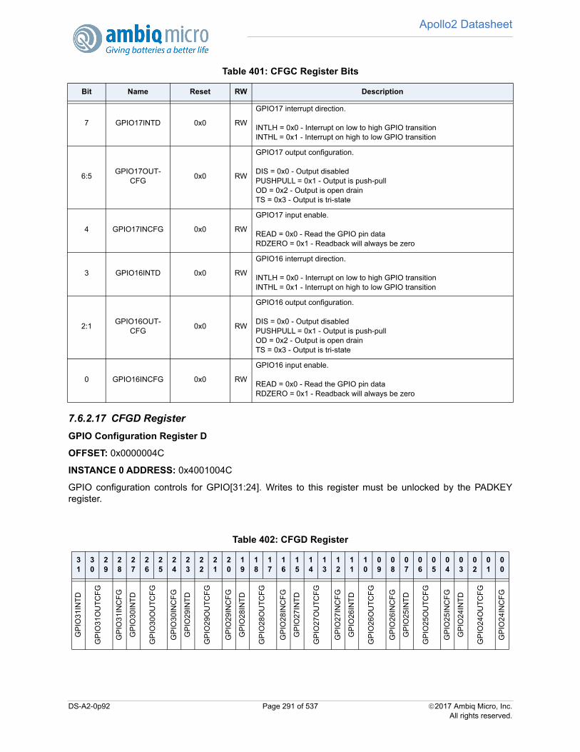
Apollo2 Datasheet
7.6.2.17 CFGD Register
GPIO Configuration Register D
OFFSET: 0x0000004C
INSTANCE 0 ADDRESS: 0x4001004C
GPIO configuration controls for GPIO[31:24]. Writes to this register must be unlocked by the PADKEYregister.
7 GPIO17INTD 0x0 RW
GPIO17 interrupt direction.
INTLH = 0x0 - Interrupt on low to high GPIO transitionINTHL = 0x1 - Interrupt on high to low GPIO transition
6:5GPIO17OUT-
CFG0x0 RW
GPIO17 output configuration.
DIS = 0x0 - Output disabledPUSHPULL = 0x1 - Output is push-pullOD = 0x2 - Output is open drainTS = 0x3 - Output is tri-state
4 GPIO17INCFG 0x0 RW
GPIO17 input enable.
READ = 0x0 - Read the GPIO pin dataRDZERO = 0x1 - Readback will always be zero
3 GPIO16INTD 0x0 RW
GPIO16 interrupt direction.
INTLH = 0x0 - Interrupt on low to high GPIO transitionINTHL = 0x1 - Interrupt on high to low GPIO transition
2:1GPIO16OUT-
CFG0x0 RW
GPIO16 output configuration.
DIS = 0x0 - Output disabledPUSHPULL = 0x1 - Output is push-pullOD = 0x2 - Output is open drainTS = 0x3 - Output is tri-state
0 GPIO16INCFG 0x0 RW
GPIO16 input enable.
READ = 0x0 - Read the GPIO pin dataRDZERO = 0x1 - Readback will always be zero
Table 402: CFGD Register
31
30
29
28
27
26
25
24
23
22
21
20
19
18
17
16
15
14
13
12
11
10
09
08
07
06
05
04
03
02
01
00
GP
IO31
INT
D
GP
IO3
1O
UT
CF
G
GP
IO3
1IN
CF
G
GP
IO30
INT
D
GP
IO3
0O
UT
CF
G
GP
IO3
0IN
CF
G
GP
IO29
INT
D
GP
IO2
9O
UT
CF
G
GP
IO2
9IN
CF
G
GP
IO28
INT
D
GP
IO2
8O
UT
CF
G
GP
IO2
8IN
CF
G
GP
IO27
INT
D
GP
IO2
7O
UT
CF
G
GP
IO2
7IN
CF
G
GP
IO26
INT
D
GP
IO2
6O
UT
CF
G
GP
IO2
6IN
CF
G
GP
IO25
INT
D
GP
IO2
5O
UT
CF
G
GP
IO2
5IN
CF
G
GP
IO24
INT
D
GP
IO2
4O
UT
CF
G
GP
IO2
4IN
CF
G
Table 401: CFGC Register Bits
Bit Name Reset RW Description
DS-A2-0p92 Page 291 of 537 2017 Ambiq Micro, Inc.All rights reserved.

Apollo2 Datasheet
Table 403: CFGD Register Bits
Bit Name Reset RW Description
31 GPIO31INTD 0x0 RW
GPIO31 interrupt direction.
INTLH = 0x0 - Interrupt on low to high GPIO transitionINTHL = 0x1 - Interrupt on high to low GPIO transition
30:29GPIO31OUT-
CFG 0x0 RW
GPIO31 output configuration.
DIS = 0x0 - Output disabledPUSHPULL = 0x1 - Output is push-pullOD = 0x2 - Output is open drainTS = 0x3 - Output is tri-state
28 GPIO31INCFG 0x0 RW
GPIO31 input enable.
READ = 0x0 - Read the GPIO pin dataRDZERO = 0x1 - Readback will always be zero
27 GPIO30INTD 0x0 RW
GPIO30 interrupt direction.
INTLH = 0x0 - Interrupt on low to high GPIO transitionINTHL = 0x1 - Interrupt on high to low GPIO transition
26:25GPIO30OUT-
CFG0x0 RW
GPIO30 output configuration.
DIS = 0x0 - Output disabledPUSHPULL = 0x1 - Output is push-pullOD = 0x2 - Output is open drainTS = 0x3 - Output is tri-state
24 GPIO30INCFG 0x0 RW
GPIO30 input enable.
READ = 0x0 - Read the GPIO pin dataRDZERO = 0x1 - Readback will always be zero
23 GPIO29INTD 0x0 RW
GPIO29 interrupt direction.
INTLH = 0x0 - Interrupt on low to high GPIO transitionINTHL = 0x1 - Interrupt on high to low GPIO transition
22:21GPIO29OUT-
CFG0x0 RW
GPIO29 output configuration.
DIS = 0x0 - Output disabledPUSHPULL = 0x1 - Output is push-pullOD = 0x2 - Output is open drainTS = 0x3 - Output is tri-state
20 GPIO29INCFG 0x0 RW
GPIO29 input enable.
READ = 0x0 - Read the GPIO pin dataRDZERO = 0x1 - Readback will always be zero
19 GPIO28INTD 0x0 RW
GPIO28 interrupt direction.
INTLH = 0x0 - Interrupt on low to high GPIO transitionINTHL = 0x1 - Interrupt on high to low GPIO transition
DS-A2-0p92 Page 292 of 537 2017 Ambiq Micro, Inc.All rights reserved.
Apollo2 Datasheet
18:17GPIO28OUT-
CFG 0x0 RW
GPIO28 output configuration.
DIS = 0x0 - Output disabledPUSHPULL = 0x1 - Output is push-pullOD = 0x2 - Output is open drainTS = 0x3 - Output is tri-state
16 GPIO28INCFG 0x0 RW
GPIO28 input enable.
READ = 0x0 - Read the GPIO pin dataRDZERO = 0x1 - Readback will always be zero
15 GPIO27INTD 0x0 RW
GPIO27 interrupt direction.
INTLH = 0x0 - Interrupt on low to high GPIO transitionINTHL = 0x1 - Interrupt on high to low GPIO transition
14:13GPIO27OUT-
CFG 0x0 RW
GPIO27 output configuration.
DIS = 0x0 - Output disabledPUSHPULL = 0x1 - Output is push-pullOD = 0x2 - Output is open drainTS = 0x3 - Output is tri-state
12 GPIO27INCFG 0x0 RW
GPIO27 input enable.
READ = 0x0 - Read the GPIO pin dataRDZERO = 0x1 - Readback will always be zero
11 GPIO26INTD 0x0 RW
GPIO26 interrupt direction.
INTLH = 0x0 - Interrupt on low to high GPIO transitionINTHL = 0x1 - Interrupt on high to low GPIO transition
10:9GPIO26OUT-
CFG 0x0 RW
GPIO26 output configuration.
DIS = 0x0 - Output disabledPUSHPULL = 0x1 - Output is push-pullOD = 0x2 - Output is open drainTS = 0x3 - Output is tri-state
8 GPIO26INCFG 0x0 RW
GPIO26 input enable.
READ = 0x0 - Read the GPIO pin dataRDZERO = 0x1 - Readback will always be zero
7 GPIO25INTD 0x0 RW
GPIO25 interrupt direction.
INTLH = 0x0 - Interrupt on low to high GPIO transitionINTHL = 0x1 - Interrupt on high to low GPIO transition
Table 403: CFGD Register Bits
Bit Name Reset RW Description
DS-A2-0p92 Page 293 of 537 2017 Ambiq Micro, Inc.All rights reserved.

Apollo2 Datasheet
7.6.2.18 CFGE Register
GPIO Configuration Register E
OFFSET: 0x00000050
INSTANCE 0 ADDRESS: 0x40010050
GPIO configuration controls for GPIO[39:32]. Writes to this register must be unlocked by the PADKEYregister.
6:5GPIO25OUT-
CFG 0x0 RW
GPIO25 output configuration.
DIS = 0x0 - Output disabledPUSHPULL = 0x1 - Output is push-pullOD = 0x2 - Output is open drainTS = 0x3 - Output is tri-state
4 GPIO25INCFG 0x0 RW
GPIO25 input enable.
READ = 0x0 - Read the GPIO pin dataRDZERO = 0x1 - Readback will always be zero
3 GPIO24INTD 0x0 RW
GPIO24 interrupt direction.
INTLH = 0x0 - Interrupt on low to high GPIO transitionINTHL = 0x1 - Interrupt on high to low GPIO transition
2:1GPIO24OUT-
CFG 0x0 RW
GPIO24 output configuration.
DIS = 0x0 - Output disabledPUSHPULL = 0x1 - Output is push-pullOD = 0x2 - Output is open drainTS = 0x3 - Output is tri-state
0 GPIO24INCFG 0x0 RW
GPIO24 input enable.
READ = 0x0 - Read the GPIO pin dataRDZERO = 0x1 - Readback will always be zero
Table 404: CFGE Register
31
30
29
28
27
26
25
24
23
22
21
20
19
18
17
16
15
14
13
12
11
10
09
08
07
06
05
04
03
02
01
00
GP
IO39
INT
D
GP
IO39
OU
TC
FG
GP
IO39
INC
FG
GP
IO38
INT
D
GP
IO38
OU
TC
FG
GP
IO3
8IN
CF
G
GP
IO37
INT
D
GP
IO37
OU
TC
FG
GP
IO3
7IN
CF
G
GP
IO36
INT
D
GP
IO36
OU
TC
FG
GP
IO36
INC
FG
GP
IO35
INT
D
GP
IO35
OU
TC
FG
GP
IO35
INC
FG
GP
IO34
INT
D
GP
IO34
OU
TC
FG
GP
IO3
4IN
CF
G
GP
IO33
INT
D
GP
IO33
OU
TC
FG
GP
IO3
3IN
CF
G
GP
IO32
INT
D
GP
IO32
OU
TC
FG
GP
IO3
2IN
CF
G
Table 403: CFGD Register Bits
Bit Name Reset RW Description
DS-A2-0p92 Page 294 of 537 2017 Ambiq Micro, Inc.All rights reserved.
Apollo2 Datasheet
Table 405: CFGE Register Bits
Bit Name Reset RW Description
31 GPIO39INTD 0x0 RW
GPIO39 interrupt direction.
INTLH = 0x0 - Interrupt on low to high GPIO transitionINTHL = 0x1 - Interrupt on high to low GPIO transition
30:29GPIO39OUT-
CFG0x0 RW
GPIO39 output configuration.
DIS = 0x0 - Output disabledPUSHPULL = 0x1 - Output is push-pullOD = 0x2 - Output is open drainTS = 0x3 - Output is tri-state
28 GPIO39INCFG 0x0 RW
GPIO39 input enable.
READ = 0x0 - Read the GPIO pin dataRDZERO = 0x1 - Readback will always be zero
27 GPIO38INTD 0x0 RW
GPIO38 interrupt direction.
INTLH = 0x0 - Interrupt on low to high GPIO transitionINTHL = 0x1 - Interrupt on high to low GPIO transition
26:25GPIO38OUT-
CFG 0x0 RW
GPIO38 output configuration.
DIS = 0x0 - Output disabledPUSHPULL = 0x1 - Output is push-pullOD = 0x2 - Output is open drainTS = 0x3 - Output is tri-state
24 GPIO38INCFG 0x0 RW
GPIO38 input enable.
READ = 0x0 - Read the GPIO pin dataRDZERO = 0x1 - Readback will always be zero
23 GPIO37INTD 0x0 RW
GPIO37 interrupt direction.
INTLH = 0x0 - Interrupt on low to high GPIO transitionINTHL = 0x1 - Interrupt on high to low GPIO transition
22:21GPIO37OUT-
CFG 0x0 RW
GPIO37 output configuration.
DIS = 0x0 - Output disabledPUSHPULL = 0x1 - Output is push-pullOD = 0x2 - Output is open drainTS = 0x3 - Output is tri-state
20 GPIO37INCFG 0x0 RW
GPIO37 input enable.
READ = 0x0 - Read the GPIO pin dataRDZERO = 0x1 - Readback will always be zero
19 GPIO36INTD 0x0 RW
GPIO36 interrupt direction.
INTLH = 0x0 - Interrupt on low to high GPIO transitionINTHL = 0x1 - Interrupt on high to low GPIO transition
DS-A2-0p92 Page 295 of 537 2017 Ambiq Micro, Inc.All rights reserved.
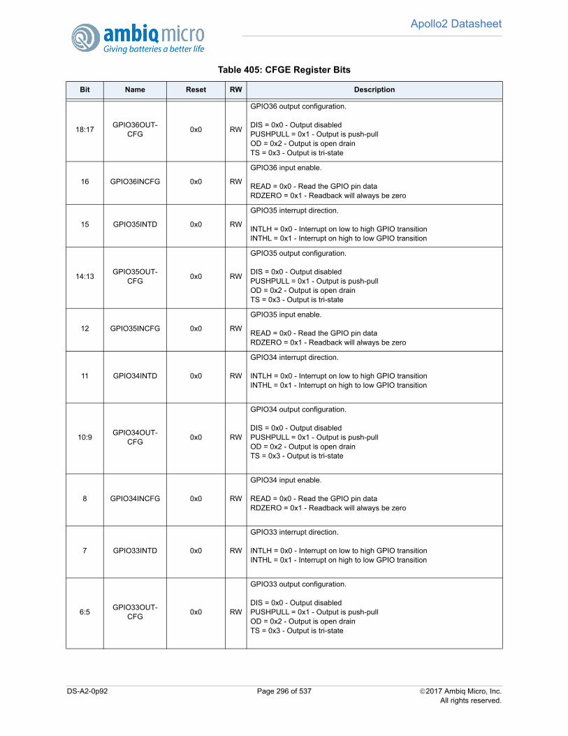
Apollo2 Datasheet
18:17GPIO36OUT-
CFG0x0 RW
GPIO36 output configuration.
DIS = 0x0 - Output disabledPUSHPULL = 0x1 - Output is push-pullOD = 0x2 - Output is open drainTS = 0x3 - Output is tri-state
16 GPIO36INCFG 0x0 RW
GPIO36 input enable.
READ = 0x0 - Read the GPIO pin dataRDZERO = 0x1 - Readback will always be zero
15 GPIO35INTD 0x0 RW
GPIO35 interrupt direction.
INTLH = 0x0 - Interrupt on low to high GPIO transitionINTHL = 0x1 - Interrupt on high to low GPIO transition
14:13GPIO35OUT-
CFG 0x0 RW
GPIO35 output configuration.
DIS = 0x0 - Output disabledPUSHPULL = 0x1 - Output is push-pullOD = 0x2 - Output is open drainTS = 0x3 - Output is tri-state
12 GPIO35INCFG 0x0 RW
GPIO35 input enable.
READ = 0x0 - Read the GPIO pin dataRDZERO = 0x1 - Readback will always be zero
11 GPIO34INTD 0x0 RW
GPIO34 interrupt direction.
INTLH = 0x0 - Interrupt on low to high GPIO transitionINTHL = 0x1 - Interrupt on high to low GPIO transition
10:9GPIO34OUT-
CFG 0x0 RW
GPIO34 output configuration.
DIS = 0x0 - Output disabledPUSHPULL = 0x1 - Output is push-pullOD = 0x2 - Output is open drainTS = 0x3 - Output is tri-state
8 GPIO34INCFG 0x0 RW
GPIO34 input enable.
READ = 0x0 - Read the GPIO pin dataRDZERO = 0x1 - Readback will always be zero
7 GPIO33INTD 0x0 RW
GPIO33 interrupt direction.
INTLH = 0x0 - Interrupt on low to high GPIO transitionINTHL = 0x1 - Interrupt on high to low GPIO transition
6:5GPIO33OUT-
CFG 0x0 RW
GPIO33 output configuration.
DIS = 0x0 - Output disabledPUSHPULL = 0x1 - Output is push-pullOD = 0x2 - Output is open drainTS = 0x3 - Output is tri-state
Table 405: CFGE Register Bits
Bit Name Reset RW Description
DS-A2-0p92 Page 296 of 537 2017 Ambiq Micro, Inc.All rights reserved.

Apollo2 Datasheet
7.6.2.19 CFGF Register
GPIO Configuration Register F
OFFSET: 0x00000054
INSTANCE 0 ADDRESS: 0x40010054
GPIO configuration controls for GPIO[47:40]. Writes to this register must be unlocked by the PADKEYregister.
4 GPIO33INCFG 0x0 RW
GPIO33 input enable.
READ = 0x0 - Read the GPIO pin dataRDZERO = 0x1 - Readback will always be zero
3 GPIO32INTD 0x0 RW
GPIO32 interrupt direction.
INTLH = 0x0 - Interrupt on low to high GPIO transitionINTHL = 0x1 - Interrupt on high to low GPIO transition
2:1GPIO32OUT-
CFG 0x0 RW
GPIO32 output configuration.
DIS = 0x0 - Output disabledPUSHPULL = 0x1 - Output is push-pullOD = 0x2 - Output is open drainTS = 0x3 - Output is tri-state
0 GPIO32INCFG 0x0 RW
GPIO32 input enable.
READ = 0x0 - Read the GPIO pin dataRDZERO = 0x1 - Readback will always be zero
Table 406: CFGF Register
31
30
29
28
27
26
25
24
23
22
21
20
19
18
17
16
15
14
13
12
11
10
09
08
07
06
05
04
03
02
01
00
GP
IO47
INT
D
GP
IO4
7O
UT
CF
G
GP
IO4
7IN
CF
G
GP
IO46
INT
D
GP
IO4
6O
UT
CF
G
GP
IO4
6IN
CF
G
GP
IO45
INT
D
GP
IO4
5O
UT
CF
G
GP
IO4
5IN
CF
G
GP
IO44
INT
D
GP
IO4
4O
UT
CF
G
GP
IO4
4IN
CF
G
GP
IO43
INT
D
GP
IO4
3O
UT
CF
G
GP
IO4
3IN
CF
G
GP
IO42
INT
D
GP
IO4
2O
UT
CF
G
GP
IO4
2IN
CF
G
GP
IO41
INT
D
GP
IO4
1O
UT
CF
G
GP
IO4
1IN
CF
G
GP
IO40
INT
D
GP
IO4
0O
UT
CF
G
GP
IO4
0IN
CF
G
Table 405: CFGE Register Bits
Bit Name Reset RW Description
DS-A2-0p92 Page 297 of 537 2017 Ambiq Micro, Inc.All rights reserved.
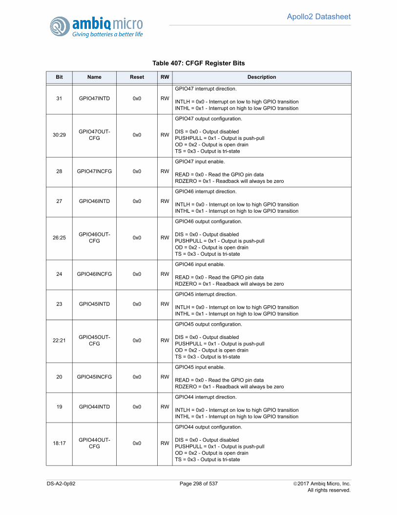
Apollo2 Datasheet
Table 407: CFGF Register Bits
Bit Name Reset RW Description
31 GPIO47INTD 0x0 RW
GPIO47 interrupt direction.
INTLH = 0x0 - Interrupt on low to high GPIO transitionINTHL = 0x1 - Interrupt on high to low GPIO transition
30:29GPIO47OUT-
CFG0x0 RW
GPIO47 output configuration.
DIS = 0x0 - Output disabledPUSHPULL = 0x1 - Output is push-pullOD = 0x2 - Output is open drainTS = 0x3 - Output is tri-state
28 GPIO47INCFG 0x0 RW
GPIO47 input enable.
READ = 0x0 - Read the GPIO pin dataRDZERO = 0x1 - Readback will always be zero
27 GPIO46INTD 0x0 RW
GPIO46 interrupt direction.
INTLH = 0x0 - Interrupt on low to high GPIO transitionINTHL = 0x1 - Interrupt on high to low GPIO transition
26:25GPIO46OUT-
CFG0x0 RW
GPIO46 output configuration.
DIS = 0x0 - Output disabledPUSHPULL = 0x1 - Output is push-pullOD = 0x2 - Output is open drainTS = 0x3 - Output is tri-state
24 GPIO46INCFG 0x0 RW
GPIO46 input enable.
READ = 0x0 - Read the GPIO pin dataRDZERO = 0x1 - Readback will always be zero
23 GPIO45INTD 0x0 RW
GPIO45 interrupt direction.
INTLH = 0x0 - Interrupt on low to high GPIO transitionINTHL = 0x1 - Interrupt on high to low GPIO transition
22:21GPIO45OUT-
CFG0x0 RW
GPIO45 output configuration.
DIS = 0x0 - Output disabledPUSHPULL = 0x1 - Output is push-pullOD = 0x2 - Output is open drainTS = 0x3 - Output is tri-state
20 GPIO45INCFG 0x0 RW
GPIO45 input enable.
READ = 0x0 - Read the GPIO pin dataRDZERO = 0x1 - Readback will always be zero
19 GPIO44INTD 0x0 RW
GPIO44 interrupt direction.
INTLH = 0x0 - Interrupt on low to high GPIO transitionINTHL = 0x1 - Interrupt on high to low GPIO transition
18:17GPIO44OUT-
CFG0x0 RW
GPIO44 output configuration.
DIS = 0x0 - Output disabledPUSHPULL = 0x1 - Output is push-pullOD = 0x2 - Output is open drainTS = 0x3 - Output is tri-state
DS-A2-0p92 Page 298 of 537 2017 Ambiq Micro, Inc.All rights reserved.
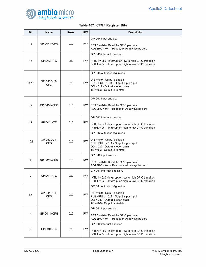
Apollo2 Datasheet
16 GPIO44INCFG 0x0 RW
GPIO44 input enable.
READ = 0x0 - Read the GPIO pin dataRDZERO = 0x1 - Readback will always be zero
15 GPIO43INTD 0x0 RW
GPIO43 interrupt direction.
INTLH = 0x0 - Interrupt on low to high GPIO transitionINTHL = 0x1 - Interrupt on high to low GPIO transition
14:13GPIO43OUT-
CFG 0x0 RW
GPIO43 output configuration.
DIS = 0x0 - Output disabledPUSHPULL = 0x1 - Output is push-pullOD = 0x2 - Output is open drainTS = 0x3 - Output is tri-state
12 GPIO43INCFG 0x0 RW
GPIO43 input enable.
READ = 0x0 - Read the GPIO pin dataRDZERO = 0x1 - Readback will always be zero
11 GPIO42INTD 0x0 RW
GPIO42 interrupt direction.
INTLH = 0x0 - Interrupt on low to high GPIO transitionINTHL = 0x1 - Interrupt on high to low GPIO transition
10:9GPIO42OUT-
CFG0x0 RW
GPIO42 output configuration.
DIS = 0x0 - Output disabledPUSHPULL = 0x1 - Output is push-pullOD = 0x2 - Output is open drainTS = 0x3 - Output is tri-state
8 GPIO42INCFG 0x0 RW
GPIO42 input enable.
READ = 0x0 - Read the GPIO pin dataRDZERO = 0x1 - Readback will always be zero
7 GPIO41INTD 0x0 RW
GPIO41 interrupt direction.
INTLH = 0x0 - Interrupt on low to high GPIO transitionINTHL = 0x1 - Interrupt on high to low GPIO transition
6:5GPIO41OUT-
CFG0x0 RW
GPIO41 output configuration.
DIS = 0x0 - Output disabledPUSHPULL = 0x1 - Output is push-pullOD = 0x2 - Output is open drainTS = 0x3 - Output is tri-state
4 GPIO41INCFG 0x0 RW
GPIO41 input enable.
READ = 0x0 - Read the GPIO pin dataRDZERO = 0x1 - Readback will always be zero
3 GPIO40INTD 0x0 RW
GPIO40 interrupt direction.
INTLH = 0x0 - Interrupt on low to high GPIO transitionINTHL = 0x1 - Interrupt on high to low GPIO transition
Table 407: CFGF Register Bits
Bit Name Reset RW Description
DS-A2-0p92 Page 299 of 537 2017 Ambiq Micro, Inc.All rights reserved.
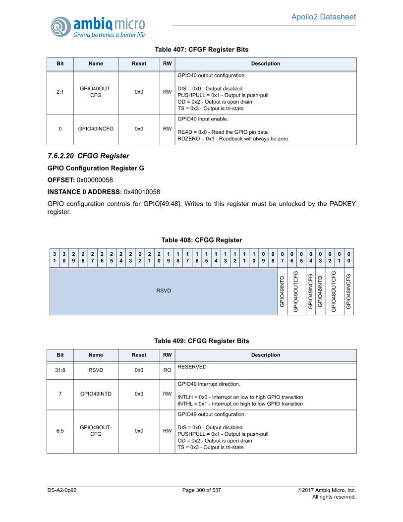
Apollo2 Datasheet
7.6.2.20 CFGG Register
GPIO Configuration Register G
OFFSET: 0x00000058
INSTANCE 0 ADDRESS: 0x40010058
GPIO configuration controls for GPIO[49:48]. Writes to this register must be unlocked by the PADKEYregister.
2:1GPIO40OUT-
CFG0x0 RW
GPIO40 output configuration.
DIS = 0x0 - Output disabledPUSHPULL = 0x1 - Output is push-pullOD = 0x2 - Output is open drainTS = 0x3 - Output is tri-state
0 GPIO40INCFG 0x0 RW
GPIO40 input enable.
READ = 0x0 - Read the GPIO pin dataRDZERO = 0x1 - Readback will always be zero
Table 408: CFGG Register
31
30
29
28
27
26
25
24
23
22
21
20
19
18
17
16
15
14
13
12
11
10
09
08
07
06
05
04
03
02
01
00
RSVD
GP
IO49
INT
D
GP
IO49
OU
TC
FG
GP
IO49
INC
FG
GP
IO48
INT
D
GP
IO48
OU
TC
FG
GP
IO48
INC
FG
Table 409: CFGG Register Bits
Bit Name Reset RW Description
31:8 RSVD 0x0 RORESERVED
7 GPIO49INTD 0x0 RW
GPIO49 interrupt direction.
INTLH = 0x0 - Interrupt on low to high GPIO transitionINTHL = 0x1 - Interrupt on high to low GPIO transition
6:5GPIO49OUT-
CFG0x0 RW
GPIO49 output configuration.
DIS = 0x0 - Output disabledPUSHPULL = 0x1 - Output is push-pullOD = 0x2 - Output is open drainTS = 0x3 - Output is tri-state
Table 407: CFGF Register Bits
Bit Name Reset RW Description
DS-A2-0p92 Page 300 of 537 2017 Ambiq Micro, Inc.All rights reserved.
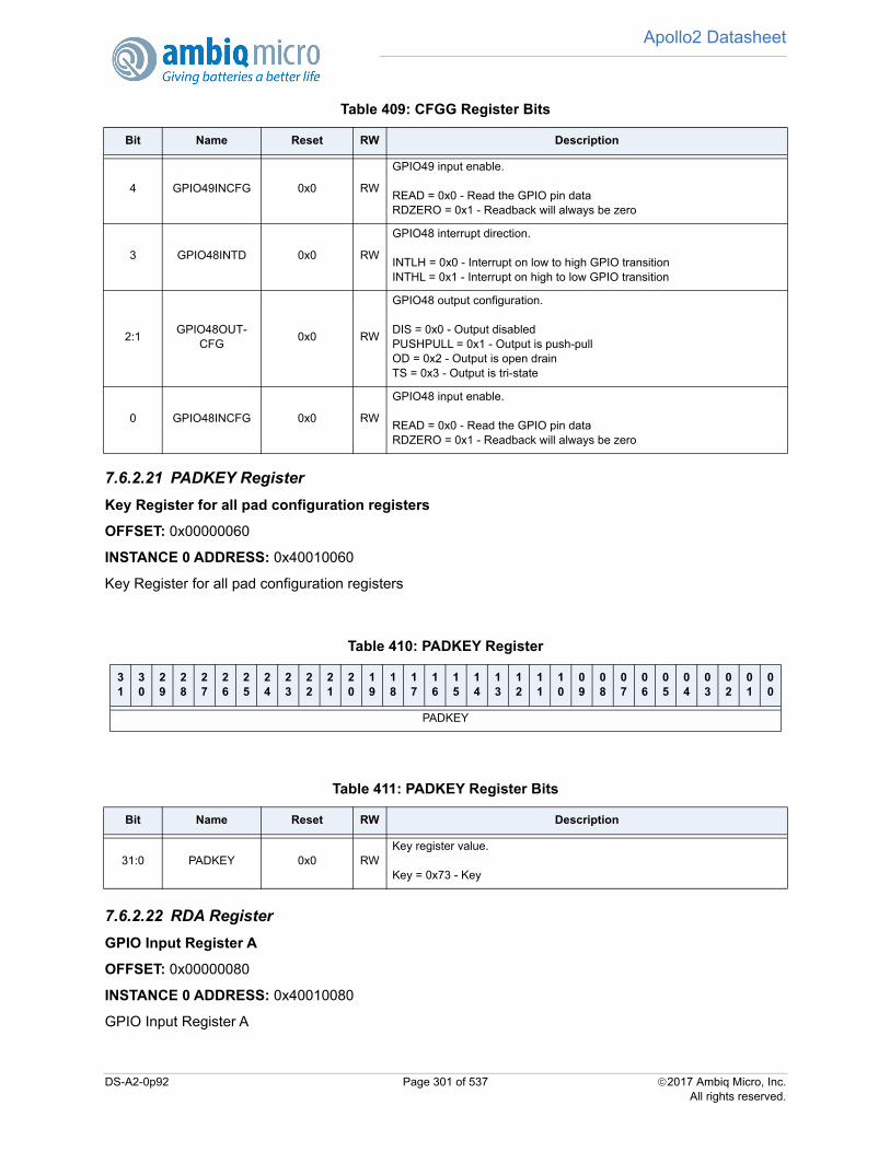
Apollo2 Datasheet
7.6.2.21 PADKEY Register
Key Register for all pad configuration registers
OFFSET: 0x00000060
INSTANCE 0 ADDRESS: 0x40010060
Key Register for all pad configuration registers
7.6.2.22 RDA Register
GPIO Input Register A
OFFSET: 0x00000080
INSTANCE 0 ADDRESS: 0x40010080
GPIO Input Register A
4 GPIO49INCFG 0x0 RW
GPIO49 input enable.
READ = 0x0 - Read the GPIO pin dataRDZERO = 0x1 - Readback will always be zero
3 GPIO48INTD 0x0 RW
GPIO48 interrupt direction.
INTLH = 0x0 - Interrupt on low to high GPIO transitionINTHL = 0x1 - Interrupt on high to low GPIO transition
2:1GPIO48OUT-
CFG0x0 RW
GPIO48 output configuration.
DIS = 0x0 - Output disabledPUSHPULL = 0x1 - Output is push-pullOD = 0x2 - Output is open drainTS = 0x3 - Output is tri-state
0 GPIO48INCFG 0x0 RW
GPIO48 input enable.
READ = 0x0 - Read the GPIO pin dataRDZERO = 0x1 - Readback will always be zero
Table 410: PADKEY Register
31
30
29
28
27
26
25
24
23
22
21
20
19
18
17
16
15
14
13
12
11
10
09
08
07
06
05
04
03
02
01
00
PADKEY
Table 411: PADKEY Register Bits
Bit Name Reset RW Description
31:0 PADKEY 0x0 RWKey register value.
Key = 0x73 - Key
Table 409: CFGG Register Bits
Bit Name Reset RW Description
DS-A2-0p92 Page 301 of 537 2017 Ambiq Micro, Inc.All rights reserved.

Apollo2 Datasheet
7.6.2.23 RDB Register
GPIO Input Register B
OFFSET: 0x00000084
INSTANCE 0 ADDRESS: 0x40010084
GPIO Input Register B
7.6.2.24 WTA Register
GPIO Output Register A
OFFSET: 0x00000088
INSTANCE 0 ADDRESS: 0x40010088
GPIO Output Register A
Table 412: RDA Register
31
30
29
28
27
26
25
24
23
22
21
20
19
18
17
16
15
14
13
12
11
10
09
08
07
06
05
04
03
02
01
00
RDA
Table 413: RDA Register Bits
Bit Name Reset RW Description
31:0 RDA 0x0 ROGPIO31-0 read data.
Table 414: RDB Register
31
30
29
28
27
26
25
24
23
22
21
20
19
18
17
16
15
14
13
12
11
10
09
08
07
06
05
04
03
02
01
00
RSVD RDB
Table 415: RDB Register Bits
Bit Name Reset RW Description
31:18 RSVD 0x0 RORESERVED
17:0 RDB 0x0 ROGPIO49-32 read data.
DS-A2-0p92 Page 302 of 537 2017 Ambiq Micro, Inc.All rights reserved.
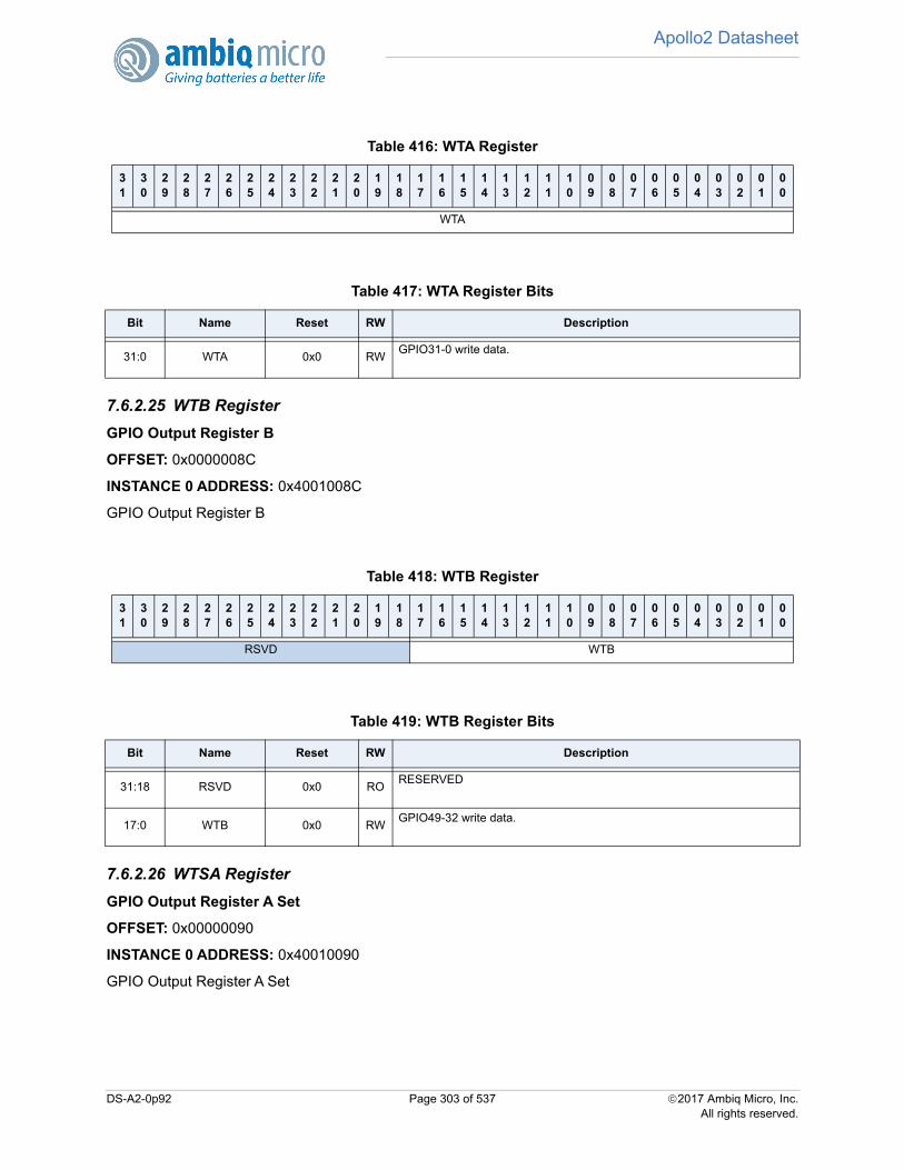
Apollo2 Datasheet
7.6.2.25 WTB Register
GPIO Output Register B
OFFSET: 0x0000008C
INSTANCE 0 ADDRESS: 0x4001008C
GPIO Output Register B
7.6.2.26 WTSA Register
GPIO Output Register A Set
OFFSET: 0x00000090
INSTANCE 0 ADDRESS: 0x40010090
GPIO Output Register A Set
Table 416: WTA Register
31
30
29
28
27
26
25
24
23
22
21
20
19
18
17
16
15
14
13
12
11
10
09
08
07
06
05
04
03
02
01
00
WTA
Table 417: WTA Register Bits
Bit Name Reset RW Description
31:0 WTA 0x0 RWGPIO31-0 write data.
Table 418: WTB Register
31
30
29
28
27
26
25
24
23
22
21
20
19
18
17
16
15
14
13
12
11
10
09
08
07
06
05
04
03
02
01
00
RSVD WTB
Table 419: WTB Register Bits
Bit Name Reset RW Description
31:18 RSVD 0x0 RORESERVED
17:0 WTB 0x0 RWGPIO49-32 write data.
DS-A2-0p92 Page 303 of 537 2017 Ambiq Micro, Inc.All rights reserved.
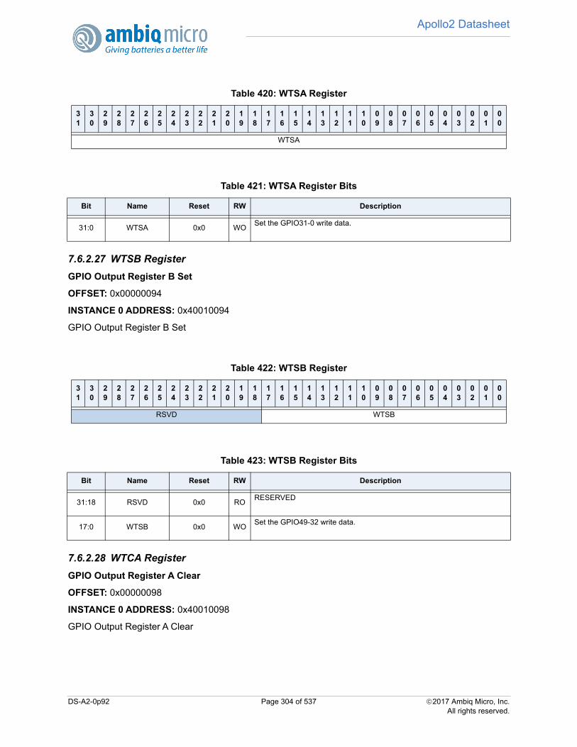
Apollo2 Datasheet
7.6.2.27 WTSB Register
GPIO Output Register B Set
OFFSET: 0x00000094
INSTANCE 0 ADDRESS: 0x40010094
GPIO Output Register B Set
7.6.2.28 WTCA Register
GPIO Output Register A Clear
OFFSET: 0x00000098
INSTANCE 0 ADDRESS: 0x40010098
GPIO Output Register A Clear
Table 420: WTSA Register
31
30
29
28
27
26
25
24
23
22
21
20
19
18
17
16
15
14
13
12
11
10
09
08
07
06
05
04
03
02
01
00
WTSA
Table 421: WTSA Register Bits
Bit Name Reset RW Description
31:0 WTSA 0x0 WOSet the GPIO31-0 write data.
Table 422: WTSB Register
31
30
29
28
27
26
25
24
23
22
21
20
19
18
17
16
15
14
13
12
11
10
09
08
07
06
05
04
03
02
01
00
RSVD WTSB
Table 423: WTSB Register Bits
Bit Name Reset RW Description
31:18 RSVD 0x0 RORESERVED
17:0 WTSB 0x0 WOSet the GPIO49-32 write data.
DS-A2-0p92 Page 304 of 537 2017 Ambiq Micro, Inc.All rights reserved.
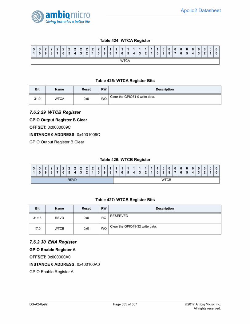
Apollo2 Datasheet
7.6.2.29 WTCB Register
GPIO Output Register B Clear
OFFSET: 0x0000009C
INSTANCE 0 ADDRESS: 0x4001009C
GPIO Output Register B Clear
7.6.2.30 ENA Register
GPIO Enable Register A
OFFSET: 0x000000A0
INSTANCE 0 ADDRESS: 0x400100A0
GPIO Enable Register A
Table 424: WTCA Register
31
30
29
28
27
26
25
24
23
22
21
20
19
18
17
16
15
14
13
12
11
10
09
08
07
06
05
04
03
02
01
00
WTCA
Table 425: WTCA Register Bits
Bit Name Reset RW Description
31:0 WTCA 0x0 WOClear the GPIO31-0 write data.
Table 426: WTCB Register
31
30
29
28
27
26
25
24
23
22
21
20
19
18
17
16
15
14
13
12
11
10
09
08
07
06
05
04
03
02
01
00
RSVD WTCB
Table 427: WTCB Register Bits
Bit Name Reset RW Description
31:18 RSVD 0x0 RORESERVED
17:0 WTCB 0x0 WOClear the GPIO49-32 write data.
DS-A2-0p92 Page 305 of 537 2017 Ambiq Micro, Inc.All rights reserved.

Apollo2 Datasheet
7.6.2.31 ENB Register
GPIO Enable Register B
OFFSET: 0x000000A4
INSTANCE 0 ADDRESS: 0x400100A4
GPIO Enable Register B
7.6.2.32 ENSA Register
GPIO Enable Register A Set
OFFSET: 0x000000A8
INSTANCE 0 ADDRESS: 0x400100A8
GPIO Enable Register A Set
Table 428: ENA Register
31
30
29
28
27
26
25
24
23
22
21
20
19
18
17
16
15
14
13
12
11
10
09
08
07
06
05
04
03
02
01
00
ENA
Table 429: ENA Register Bits
Bit Name Reset RW Description
31:0 ENA 0x0 RWGPIO31-0 output enables
Table 430: ENB Register
31
30
29
28
27
26
25
24
23
22
21
20
19
18
17
16
15
14
13
12
11
10
09
08
07
06
05
04
03
02
01
00
RSVD ENB
Table 431: ENB Register Bits
Bit Name Reset RW Description
31:18 RSVD 0x0 RORESERVED
17:0 ENB 0x0 RWGPIO49-32 output enables
DS-A2-0p92 Page 306 of 537 2017 Ambiq Micro, Inc.All rights reserved.
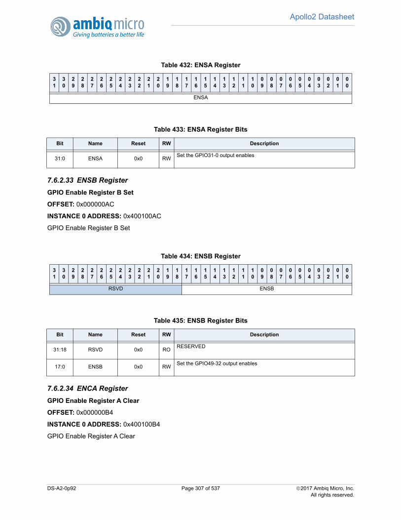
Apollo2 Datasheet
7.6.2.33 ENSB Register
GPIO Enable Register B Set
OFFSET: 0x000000AC
INSTANCE 0 ADDRESS: 0x400100AC
GPIO Enable Register B Set
7.6.2.34 ENCA Register
GPIO Enable Register A Clear
OFFSET: 0x000000B4
INSTANCE 0 ADDRESS: 0x400100B4
GPIO Enable Register A Clear
Table 432: ENSA Register
31
30
29
28
27
26
25
24
23
22
21
20
19
18
17
16
15
14
13
12
11
10
09
08
07
06
05
04
03
02
01
00
ENSA
Table 433: ENSA Register Bits
Bit Name Reset RW Description
31:0 ENSA 0x0 RWSet the GPIO31-0 output enables
Table 434: ENSB Register
31
30
29
28
27
26
25
24
23
22
21
20
19
18
17
16
15
14
13
12
11
10
09
08
07
06
05
04
03
02
01
00
RSVD ENSB
Table 435: ENSB Register Bits
Bit Name Reset RW Description
31:18 RSVD 0x0 RORESERVED
17:0 ENSB 0x0 RWSet the GPIO49-32 output enables
DS-A2-0p92 Page 307 of 537 2017 Ambiq Micro, Inc.All rights reserved.

Apollo2 Datasheet
7.6.2.35 ENCB Register
GPIO Enable Register B Clear
OFFSET: 0x000000B8
INSTANCE 0 ADDRESS: 0x400100B8
GPIO Enable Register B Clear
7.6.2.36 STMRCAP Register
STIMER Capture Control
OFFSET: 0x000000BC
INSTANCE 0 ADDRESS: 0x400100BC
STIMER Capture trigger select and enable.
Table 436: ENCA Register
31
30
29
28
27
26
25
24
23
22
21
20
19
18
17
16
15
14
13
12
11
10
09
08
07
06
05
04
03
02
01
00
ENCA
Table 437: ENCA Register Bits
Bit Name Reset RW Description
31:0 ENCA 0x0 RWClear the GPIO31-0 output enables
Table 438: ENCB Register
31
30
29
28
27
26
25
24
23
22
21
20
19
18
17
16
15
14
13
12
11
10
09
08
07
06
05
04
03
02
01
00
RSVD ENCB
Table 439: ENCB Register Bits
Bit Name Reset RW Description
31:18 RSVD 0x0 RORESERVED
17:0 ENCB 0x0 RWClear the GPIO49-32 output enables
DS-A2-0p92 Page 308 of 537 2017 Ambiq Micro, Inc.All rights reserved.
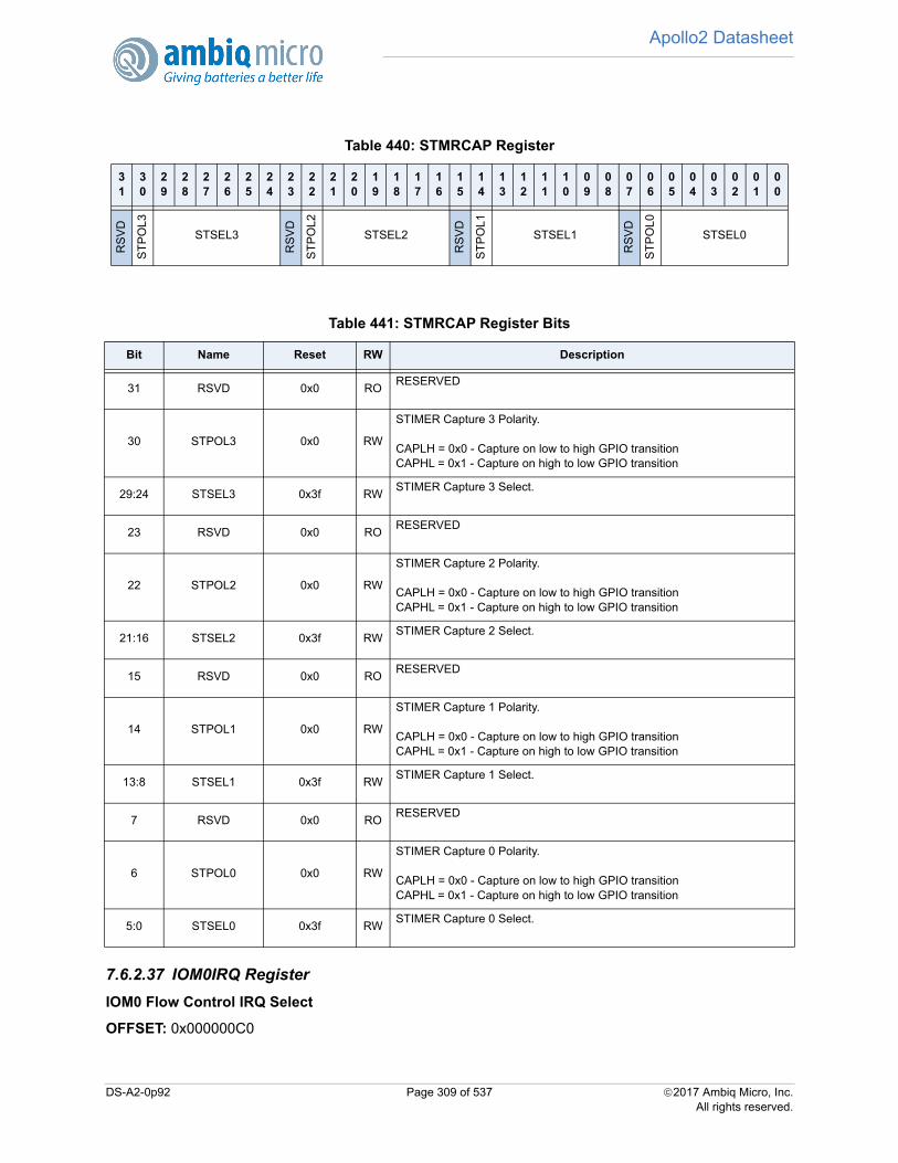
Apollo2 Datasheet
7.6.2.37 IOM0IRQ Register
IOM0 Flow Control IRQ Select
OFFSET: 0x000000C0
Table 440: STMRCAP Register
31
30
29
28
27
26
25
24
23
22
21
20
19
18
17
16
15
14
13
12
11
10
09
08
07
06
05
04
03
02
01
00
RS
VD
ST
PO
L3
STSEL3
RS
VD
ST
PO
L2
STSEL2
RS
VD
ST
PO
L1
STSEL1
RS
VD
ST
PO
L0
STSEL0
Table 441: STMRCAP Register Bits
Bit Name Reset RW Description
31 RSVD 0x0 RORESERVED
30 STPOL3 0x0 RW
STIMER Capture 3 Polarity.
CAPLH = 0x0 - Capture on low to high GPIO transitionCAPHL = 0x1 - Capture on high to low GPIO transition
29:24 STSEL3 0x3f RWSTIMER Capture 3 Select.
23 RSVD 0x0 RORESERVED
22 STPOL2 0x0 RW
STIMER Capture 2 Polarity.
CAPLH = 0x0 - Capture on low to high GPIO transitionCAPHL = 0x1 - Capture on high to low GPIO transition
21:16 STSEL2 0x3f RWSTIMER Capture 2 Select.
15 RSVD 0x0 RORESERVED
14 STPOL1 0x0 RW
STIMER Capture 1 Polarity.
CAPLH = 0x0 - Capture on low to high GPIO transitionCAPHL = 0x1 - Capture on high to low GPIO transition
13:8 STSEL1 0x3f RWSTIMER Capture 1 Select.
7 RSVD 0x0 RORESERVED
6 STPOL0 0x0 RW
STIMER Capture 0 Polarity.
CAPLH = 0x0 - Capture on low to high GPIO transitionCAPHL = 0x1 - Capture on high to low GPIO transition
5:0 STSEL0 0x3f RWSTIMER Capture 0 Select.
DS-A2-0p92 Page 309 of 537 2017 Ambiq Micro, Inc.All rights reserved.
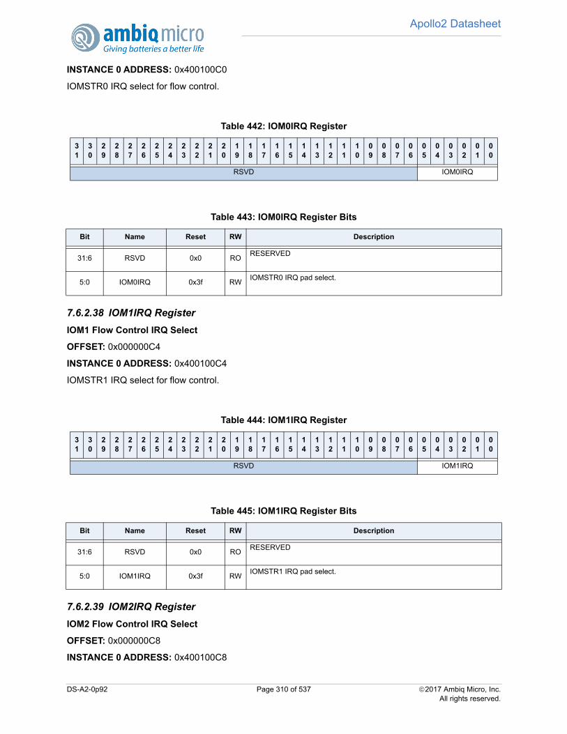
Apollo2 Datasheet
INSTANCE 0 ADDRESS: 0x400100C0
IOMSTR0 IRQ select for flow control.
7.6.2.38 IOM1IRQ Register
IOM1 Flow Control IRQ Select
OFFSET: 0x000000C4
INSTANCE 0 ADDRESS: 0x400100C4
IOMSTR1 IRQ select for flow control.
7.6.2.39 IOM2IRQ Register
IOM2 Flow Control IRQ Select
OFFSET: 0x000000C8
INSTANCE 0 ADDRESS: 0x400100C8
Table 442: IOM0IRQ Register
31
30
29
28
27
26
25
24
23
22
21
20
19
18
17
16
15
14
13
12
11
10
09
08
07
06
05
04
03
02
01
00
RSVD IOM0IRQ
Table 443: IOM0IRQ Register Bits
Bit Name Reset RW Description
31:6 RSVD 0x0 RORESERVED
5:0 IOM0IRQ 0x3f RWIOMSTR0 IRQ pad select.
Table 444: IOM1IRQ Register
31
30
29
28
27
26
25
24
23
22
21
20
19
18
17
16
15
14
13
12
11
10
09
08
07
06
05
04
03
02
01
00
RSVD IOM1IRQ
Table 445: IOM1IRQ Register Bits
Bit Name Reset RW Description
31:6 RSVD 0x0 RORESERVED
5:0 IOM1IRQ 0x3f RWIOMSTR1 IRQ pad select.
DS-A2-0p92 Page 310 of 537 2017 Ambiq Micro, Inc.All rights reserved.

Apollo2 Datasheet
IOMSTR2 IRQ select for flow control.
7.6.2.40 IOM3IRQ Register
IOM3 Flow Control IRQ Select
OFFSET: 0x000000CC
INSTANCE 0 ADDRESS: 0x400100CC
IOMSTR3 IRQ select for flow control.
7.6.2.41 IOM4IRQ Register
IOM4 Flow Control IRQ Select
OFFSET: 0x000000D0
INSTANCE 0 ADDRESS: 0x400100D0
IOMSTR4 IRQ select for flow control.
Table 446: IOM2IRQ Register
31
30
29
28
27
26
25
24
23
22
21
20
19
18
17
16
15
14
13
12
11
10
09
08
07
06
05
04
03
02
01
00
RSVD IOM2IRQ
Table 447: IOM2IRQ Register Bits
Bit Name Reset RW Description
31:6 RSVD 0x0 RORESERVED
5:0 IOM2IRQ 0x3f RWIOMSTR2 IRQ pad select.
Table 448: IOM3IRQ Register
31
30
29
28
27
26
25
24
23
22
21
20
19
18
17
16
15
14
13
12
11
10
09
08
07
06
05
04
03
02
01
00
RSVD IOM3IRQ
Table 449: IOM3IRQ Register Bits
Bit Name Reset RW Description
31:6 RSVD 0x0 RORESERVED
5:0 IOM3IRQ 0x3f RWIOMSTR3 IRQ pad select.
DS-A2-0p92 Page 311 of 537 2017 Ambiq Micro, Inc.All rights reserved.
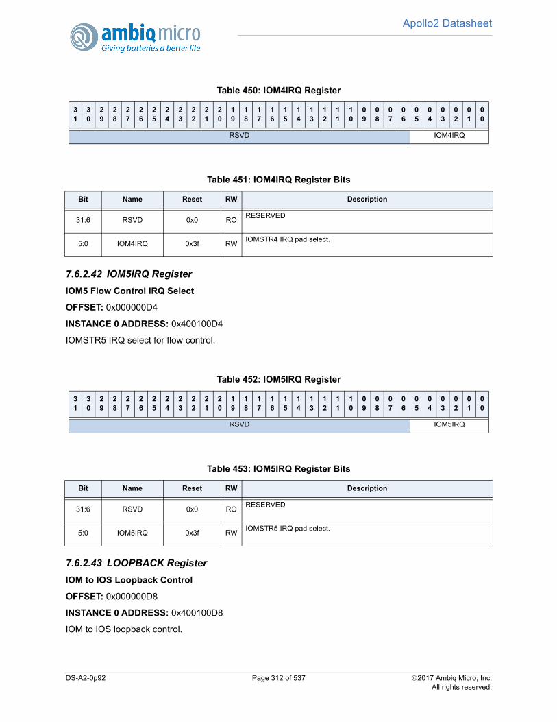
Apollo2 Datasheet
7.6.2.42 IOM5IRQ Register
IOM5 Flow Control IRQ Select
OFFSET: 0x000000D4
INSTANCE 0 ADDRESS: 0x400100D4
IOMSTR5 IRQ select for flow control.
7.6.2.43 LOOPBACK Register
IOM to IOS Loopback Control
OFFSET: 0x000000D8
INSTANCE 0 ADDRESS: 0x400100D8
IOM to IOS loopback control.
Table 450: IOM4IRQ Register
31
30
29
28
27
26
25
24
23
22
21
20
19
18
17
16
15
14
13
12
11
10
09
08
07
06
05
04
03
02
01
00
RSVD IOM4IRQ
Table 451: IOM4IRQ Register Bits
Bit Name Reset RW Description
31:6 RSVD 0x0 RORESERVED
5:0 IOM4IRQ 0x3f RWIOMSTR4 IRQ pad select.
Table 452: IOM5IRQ Register
31
30
29
28
27
26
25
24
23
22
21
20
19
18
17
16
15
14
13
12
11
10
09
08
07
06
05
04
03
02
01
00
RSVD IOM5IRQ
Table 453: IOM5IRQ Register Bits
Bit Name Reset RW Description
31:6 RSVD 0x0 RORESERVED
5:0 IOM5IRQ 0x3f RWIOMSTR5 IRQ pad select.
DS-A2-0p92 Page 312 of 537 2017 Ambiq Micro, Inc.All rights reserved.
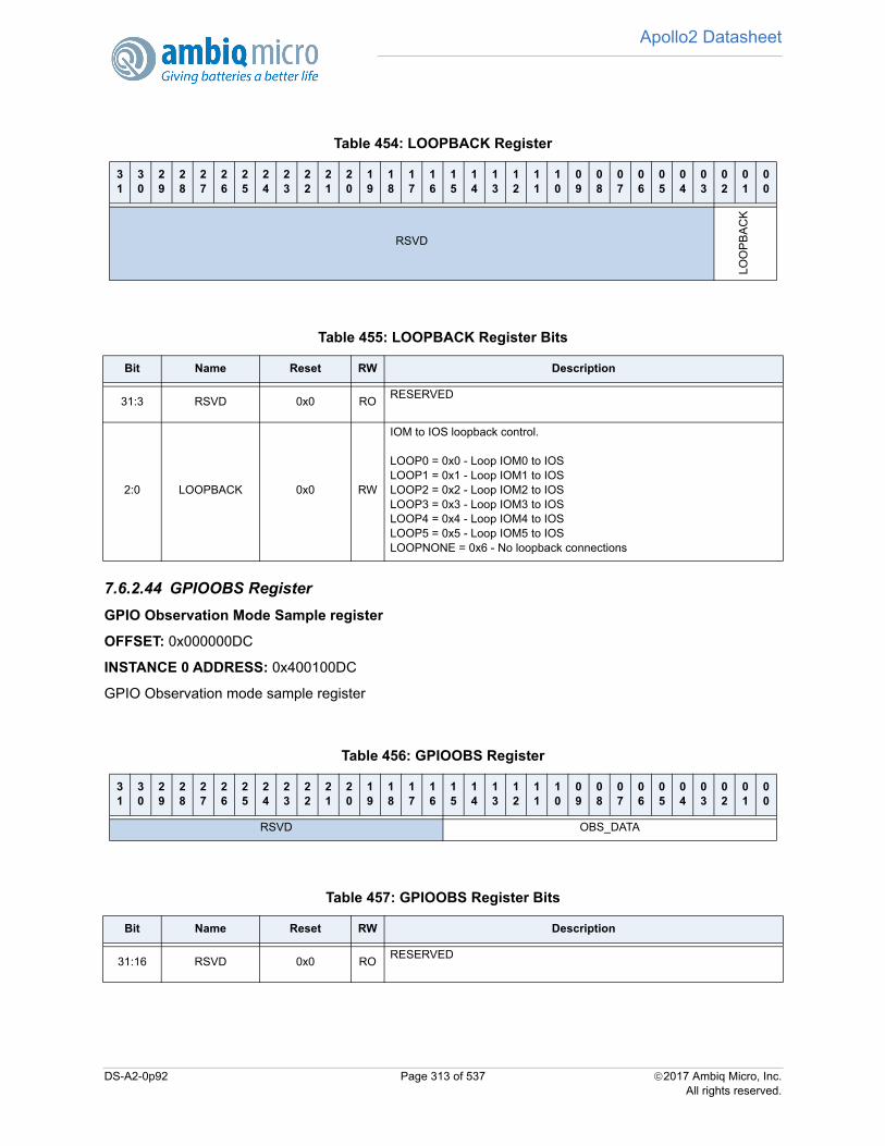
Apollo2 Datasheet
7.6.2.44 GPIOOBS Register
GPIO Observation Mode Sample register
OFFSET: 0x000000DC
INSTANCE 0 ADDRESS: 0x400100DC
GPIO Observation mode sample register
Table 454: LOOPBACK Register
31
30
29
28
27
26
25
24
23
22
21
20
19
18
17
16
15
14
13
12
11
10
09
08
07
06
05
04
03
02
01
00
RSVD
LOO
PB
AC
K
Table 455: LOOPBACK Register Bits
Bit Name Reset RW Description
31:3 RSVD 0x0 RORESERVED
2:0 LOOPBACK 0x0 RW
IOM to IOS loopback control.
LOOP0 = 0x0 - Loop IOM0 to IOSLOOP1 = 0x1 - Loop IOM1 to IOSLOOP2 = 0x2 - Loop IOM2 to IOSLOOP3 = 0x3 - Loop IOM3 to IOSLOOP4 = 0x4 - Loop IOM4 to IOSLOOP5 = 0x5 - Loop IOM5 to IOSLOOPNONE = 0x6 - No loopback connections
Table 456: GPIOOBS Register
31
30
29
28
27
26
25
24
23
22
21
20
19
18
17
16
15
14
13
12
11
10
09
08
07
06
05
04
03
02
01
00
RSVD OBS_DATA
Table 457: GPIOOBS Register Bits
Bit Name Reset RW Description
31:16 RSVD 0x0 RORESERVED
DS-A2-0p92 Page 313 of 537 2017 Ambiq Micro, Inc.All rights reserved.
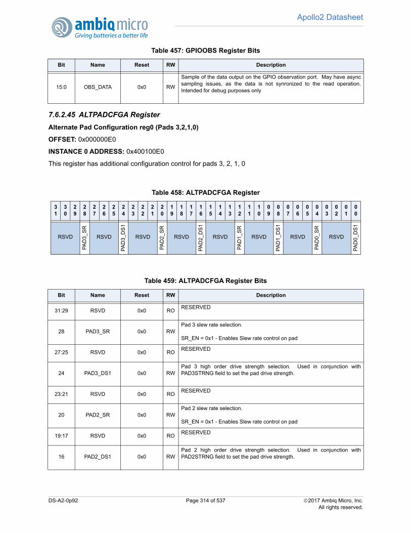
Apollo2 Datasheet
7.6.2.45 ALTPADCFGA Register
Alternate Pad Configuration reg0 (Pads 3,2,1,0)
OFFSET: 0x000000E0
INSTANCE 0 ADDRESS: 0x400100E0
This register has additional configuration control for pads 3, 2, 1, 0
15:0 OBS_DATA 0x0 RW
Sample of the data output on the GPIO observation port. May have asyncsampling issues, as the data is not synronized to the read operation.Intended for debug purposes only
Table 458: ALTPADCFGA Register
31
30
29
28
27
26
25
24
23
22
21
20
19
18
17
16
15
14
13
12
11
10
09
08
07
06
05
04
03
02
01
00
RSVD
PA
D3_
SR
RSVD
PA
D3_
DS
1
RSVD
PA
D2_
SR
RSVD
PA
D2_
DS
1
RSVDP
AD
1_S
RRSVD
PA
D1_
DS
1
RSVD
PA
D0_
SR
RSVD
PA
D0_
DS
1
Table 459: ALTPADCFGA Register Bits
Bit Name Reset RW Description
31:29 RSVD 0x0 RORESERVED
28 PAD3_SR 0x0 RWPad 3 slew rate selection.
SR_EN = 0x1 - Enables Slew rate control on pad
27:25 RSVD 0x0 RORESERVED
24 PAD3_DS1 0x0 RWPad 3 high order drive strength selection. Used in conjunction withPAD3STRNG field to set the pad drive strength.
23:21 RSVD 0x0 RORESERVED
20 PAD2_SR 0x0 RWPad 2 slew rate selection.
SR_EN = 0x1 - Enables Slew rate control on pad
19:17 RSVD 0x0 RORESERVED
16 PAD2_DS1 0x0 RWPad 2 high order drive strength selection. Used in conjunction withPAD2STRNG field to set the pad drive strength.
Table 457: GPIOOBS Register Bits
Bit Name Reset RW Description
DS-A2-0p92 Page 314 of 537 2017 Ambiq Micro, Inc.All rights reserved.
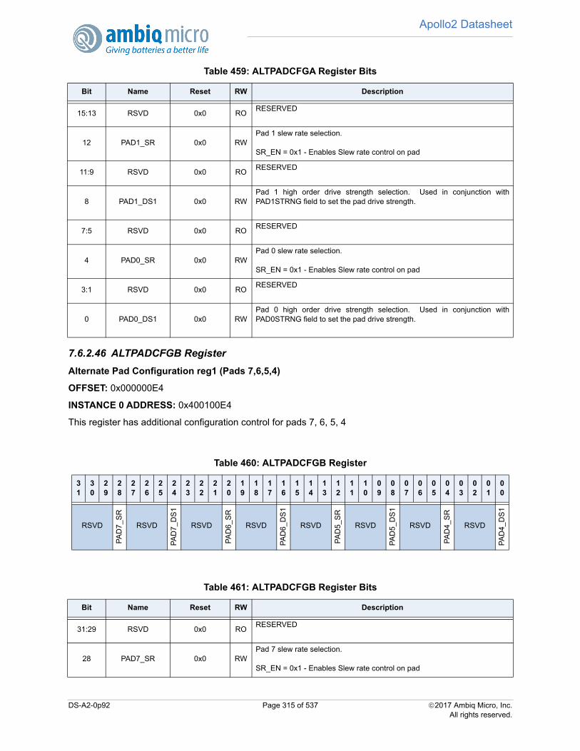
Apollo2 Datasheet
7.6.2.46 ALTPADCFGB Register
Alternate Pad Configuration reg1 (Pads 7,6,5,4)
OFFSET: 0x000000E4
INSTANCE 0 ADDRESS: 0x400100E4
This register has additional configuration control for pads 7, 6, 5, 4
15:13 RSVD 0x0 RORESERVED
12 PAD1_SR 0x0 RWPad 1 slew rate selection.
SR_EN = 0x1 - Enables Slew rate control on pad
11:9 RSVD 0x0 RORESERVED
8 PAD1_DS1 0x0 RWPad 1 high order drive strength selection. Used in conjunction withPAD1STRNG field to set the pad drive strength.
7:5 RSVD 0x0 RORESERVED
4 PAD0_SR 0x0 RWPad 0 slew rate selection.
SR_EN = 0x1 - Enables Slew rate control on pad
3:1 RSVD 0x0 RORESERVED
0 PAD0_DS1 0x0 RWPad 0 high order drive strength selection. Used in conjunction withPAD0STRNG field to set the pad drive strength.
Table 460: ALTPADCFGB Register
31
30
29
28
27
26
25
24
23
22
21
20
19
18
17
16
15
14
13
12
11
10
09
08
07
06
05
04
03
02
01
00
RSVD
PA
D7_
SR
RSVD
PA
D7_
DS
1
RSVD
PA
D6_
SR
RSVD
PA
D6_
DS
1
RSVD
PA
D5_
SR
RSVD
PA
D5_
DS
1
RSVD
PA
D4_
SR
RSVD
PA
D4_
DS
1
Table 461: ALTPADCFGB Register Bits
Bit Name Reset RW Description
31:29 RSVD 0x0 RORESERVED
28 PAD7_SR 0x0 RWPad 7 slew rate selection.
SR_EN = 0x1 - Enables Slew rate control on pad
Table 459: ALTPADCFGA Register Bits
Bit Name Reset RW Description
DS-A2-0p92 Page 315 of 537 2017 Ambiq Micro, Inc.All rights reserved.
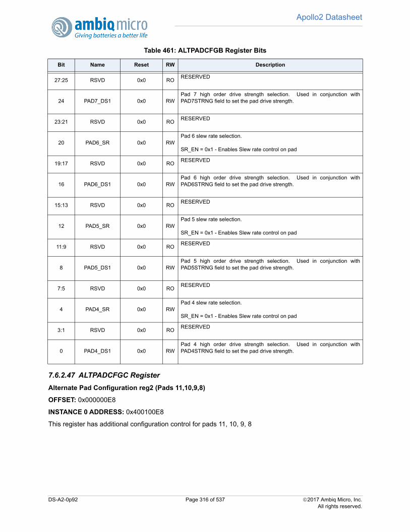
Apollo2 Datasheet
7.6.2.47 ALTPADCFGC Register
Alternate Pad Configuration reg2 (Pads 11,10,9,8)
OFFSET: 0x000000E8
INSTANCE 0 ADDRESS: 0x400100E8
This register has additional configuration control for pads 11, 10, 9, 8
27:25 RSVD 0x0 RORESERVED
24 PAD7_DS1 0x0 RWPad 7 high order drive strength selection. Used in conjunction withPAD7STRNG field to set the pad drive strength.
23:21 RSVD 0x0 RORESERVED
20 PAD6_SR 0x0 RWPad 6 slew rate selection.
SR_EN = 0x1 - Enables Slew rate control on pad
19:17 RSVD 0x0 RORESERVED
16 PAD6_DS1 0x0 RWPad 6 high order drive strength selection. Used in conjunction withPAD6STRNG field to set the pad drive strength.
15:13 RSVD 0x0 RORESERVED
12 PAD5_SR 0x0 RWPad 5 slew rate selection.
SR_EN = 0x1 - Enables Slew rate control on pad
11:9 RSVD 0x0 RORESERVED
8 PAD5_DS1 0x0 RWPad 5 high order drive strength selection. Used in conjunction withPAD5STRNG field to set the pad drive strength.
7:5 RSVD 0x0 RORESERVED
4 PAD4_SR 0x0 RWPad 4 slew rate selection.
SR_EN = 0x1 - Enables Slew rate control on pad
3:1 RSVD 0x0 RORESERVED
0 PAD4_DS1 0x0 RWPad 4 high order drive strength selection. Used in conjunction withPAD4STRNG field to set the pad drive strength.
Table 461: ALTPADCFGB Register Bits
Bit Name Reset RW Description
DS-A2-0p92 Page 316 of 537 2017 Ambiq Micro, Inc.All rights reserved.
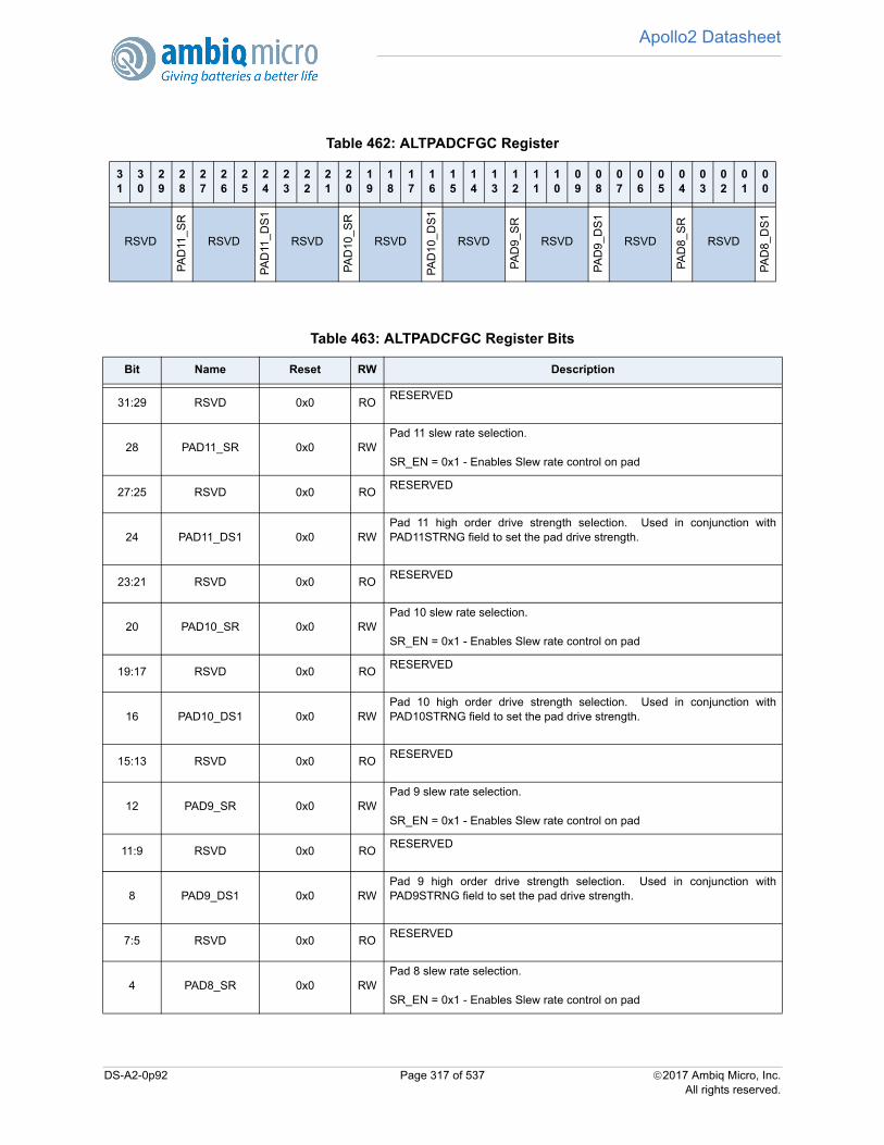
Apollo2 Datasheet
Table 462: ALTPADCFGC Register
31
30
29
28
27
26
25
24
23
22
21
20
19
18
17
16
15
14
13
12
11
10
09
08
07
06
05
04
03
02
01
00
RSVD
PA
D11
_S
R
RSVD
PA
D11
_D
S1
RSVD
PA
D10
_SR
RSVD
PA
D10
_DS
1
RSVD
PA
D9_
SR
RSVD
PA
D9_
DS
1
RSVD
PA
D8_
SR
RSVD
PA
D8_
DS
1
Table 463: ALTPADCFGC Register Bits
Bit Name Reset RW Description
31:29 RSVD 0x0 RORESERVED
28 PAD11_SR 0x0 RWPad 11 slew rate selection.
SR_EN = 0x1 - Enables Slew rate control on pad
27:25 RSVD 0x0 RORESERVED
24 PAD11_DS1 0x0 RWPad 11 high order drive strength selection. Used in conjunction withPAD11STRNG field to set the pad drive strength.
23:21 RSVD 0x0 RORESERVED
20 PAD10_SR 0x0 RWPad 10 slew rate selection.
SR_EN = 0x1 - Enables Slew rate control on pad
19:17 RSVD 0x0 RORESERVED
16 PAD10_DS1 0x0 RWPad 10 high order drive strength selection. Used in conjunction withPAD10STRNG field to set the pad drive strength.
15:13 RSVD 0x0 RORESERVED
12 PAD9_SR 0x0 RWPad 9 slew rate selection.
SR_EN = 0x1 - Enables Slew rate control on pad
11:9 RSVD 0x0 RORESERVED
8 PAD9_DS1 0x0 RWPad 9 high order drive strength selection. Used in conjunction withPAD9STRNG field to set the pad drive strength.
7:5 RSVD 0x0 RORESERVED
4 PAD8_SR 0x0 RWPad 8 slew rate selection.
SR_EN = 0x1 - Enables Slew rate control on pad
DS-A2-0p92 Page 317 of 537 2017 Ambiq Micro, Inc.All rights reserved.
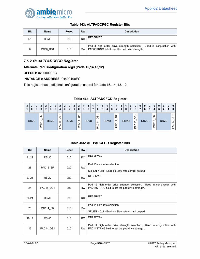
Apollo2 Datasheet
7.6.2.48 ALTPADCFGD Register
Alternate Pad Configuration reg3 (Pads 15,14,13,12)
OFFSET: 0x000000EC
INSTANCE 0 ADDRESS: 0x400100EC
This register has additional configuration control for pads 15, 14, 13, 12
3:1 RSVD 0x0 RORESERVED
0 PAD8_DS1 0x0 RWPad 8 high order drive strength selection. Used in conjunction withPAD8STRNG field to set the pad drive strength.
Table 464: ALTPADCFGD Register
31
30
29
28
27
26
25
24
23
22
21
20
19
18
17
16
15
14
13
12
11
10
09
08
07
06
05
04
03
02
01
00
RSVD
PA
D15
_SR
RSVD
PA
D15
_DS
1
RSVD
PA
D14
_SR
RSVD
PA
D14
_DS
1
RSVD
PA
D13
_SR
RSVD
PA
D13
_DS
1
RSVD
PA
D12
_SR
RSVD
PA
D12
_DS
1
Table 465: ALTPADCFGD Register Bits
Bit Name Reset RW Description
31:29 RSVD 0x0 RORESERVED
28 PAD15_SR 0x0 RWPad 15 slew rate selection.
SR_EN = 0x1 - Enables Slew rate control on pad
27:25 RSVD 0x0 RORESERVED
24 PAD15_DS1 0x0 RWPad 15 high order drive strength selection. Used in conjunction withPAD15STRNG field to set the pad drive strength.
23:21 RSVD 0x0 RORESERVED
20 PAD14_SR 0x0 RWPad 14 slew rate selection.
SR_EN = 0x1 - Enables Slew rate control on pad
19:17 RSVD 0x0 RORESERVED
16 PAD14_DS1 0x0 RWPad 14 high order drive strength selection. Used in conjunction withPAD14STRNG field to set the pad drive strength.
Table 463: ALTPADCFGC Register Bits
Bit Name Reset RW Description
DS-A2-0p92 Page 318 of 537 2017 Ambiq Micro, Inc.All rights reserved.

Apollo2 Datasheet
7.6.2.49 ALTPADCFGE Register
Alternate Pad Configuration reg4 (Pads 19,18,17,16)
OFFSET: 0x000000F0
INSTANCE 0 ADDRESS: 0x400100F0
This register has additional configuration control for pads 19, 18, 17, 16
15:13 RSVD 0x0 RORESERVED
12 PAD13_SR 0x0 RWPad 13 slew rate selection.
SR_EN = 0x1 - Enables Slew rate control on pad
11:9 RSVD 0x0 RORESERVED
8 PAD13_DS1 0x0 RWPad 13 high order drive strength selection. Used in conjunction withPAD13STRNG field to set the pad drive strength.
7:5 RSVD 0x0 RORESERVED
4 PAD12_SR 0x0 RWPad 12 slew rate selection.
SR_EN = 0x1 - Enables Slew rate control on pad
3:1 RSVD 0x0 RORESERVED
0 PAD12_DS1 0x0 RWPad 12 high order drive strength selection. Used in conjunction withPAD12STRNG field to set the pad drive strength.
Table 466: ALTPADCFGE Register
31
30
29
28
27
26
25
24
23
22
21
20
19
18
17
16
15
14
13
12
11
10
09
08
07
06
05
04
03
02
01
00
RSVD
PA
D19
_SR
RSVD
PA
D19
_DS
1
RSVD
PA
D18
_SR
RSVD
PA
D18
_DS
1
RSVD
PA
D17
_SR
RSVD
PA
D17
_DS
1
RSVD
PA
D16
_SR
RSVD
PA
D16
_DS
1
Table 467: ALTPADCFGE Register Bits
Bit Name Reset RW Description
31:29 RSVD 0x0 RORESERVED
28 PAD19_SR 0x0 RWPad 19 slew rate selection.
SR_EN = 0x1 - Enables Slew rate control on pad
Table 465: ALTPADCFGD Register Bits
Bit Name Reset RW Description
DS-A2-0p92 Page 319 of 537 2017 Ambiq Micro, Inc.All rights reserved.
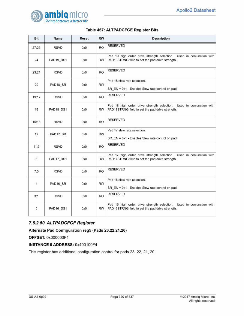
Apollo2 Datasheet
7.6.2.50 ALTPADCFGF Register
Alternate Pad Configuration reg5 (Pads 23,22,21,20)
OFFSET: 0x000000F4
INSTANCE 0 ADDRESS: 0x400100F4
This register has additional configuration control for pads 23, 22, 21, 20
27:25 RSVD 0x0 RORESERVED
24 PAD19_DS1 0x0 RWPad 19 high order drive strength selection. Used in conjunction withPAD19STRNG field to set the pad drive strength.
23:21 RSVD 0x0 RORESERVED
20 PAD18_SR 0x0 RWPad 18 slew rate selection.
SR_EN = 0x1 - Enables Slew rate control on pad
19:17 RSVD 0x0 RORESERVED
16 PAD18_DS1 0x0 RWPad 18 high order drive strength selection. Used in conjunction withPAD18STRNG field to set the pad drive strength.
15:13 RSVD 0x0 RORESERVED
12 PAD17_SR 0x0 RWPad 17 slew rate selection.
SR_EN = 0x1 - Enables Slew rate control on pad
11:9 RSVD 0x0 RORESERVED
8 PAD17_DS1 0x0 RWPad 17 high order drive strength selection. Used in conjunction withPAD17STRNG field to set the pad drive strength.
7:5 RSVD 0x0 RORESERVED
4 PAD16_SR 0x0 RWPad 16 slew rate selection.
SR_EN = 0x1 - Enables Slew rate control on pad
3:1 RSVD 0x0 RORESERVED
0 PAD16_DS1 0x0 RWPad 16 high order drive strength selection. Used in conjunction withPAD16STRNG field to set the pad drive strength.
Table 467: ALTPADCFGE Register Bits
Bit Name Reset RW Description
DS-A2-0p92 Page 320 of 537 2017 Ambiq Micro, Inc.All rights reserved.
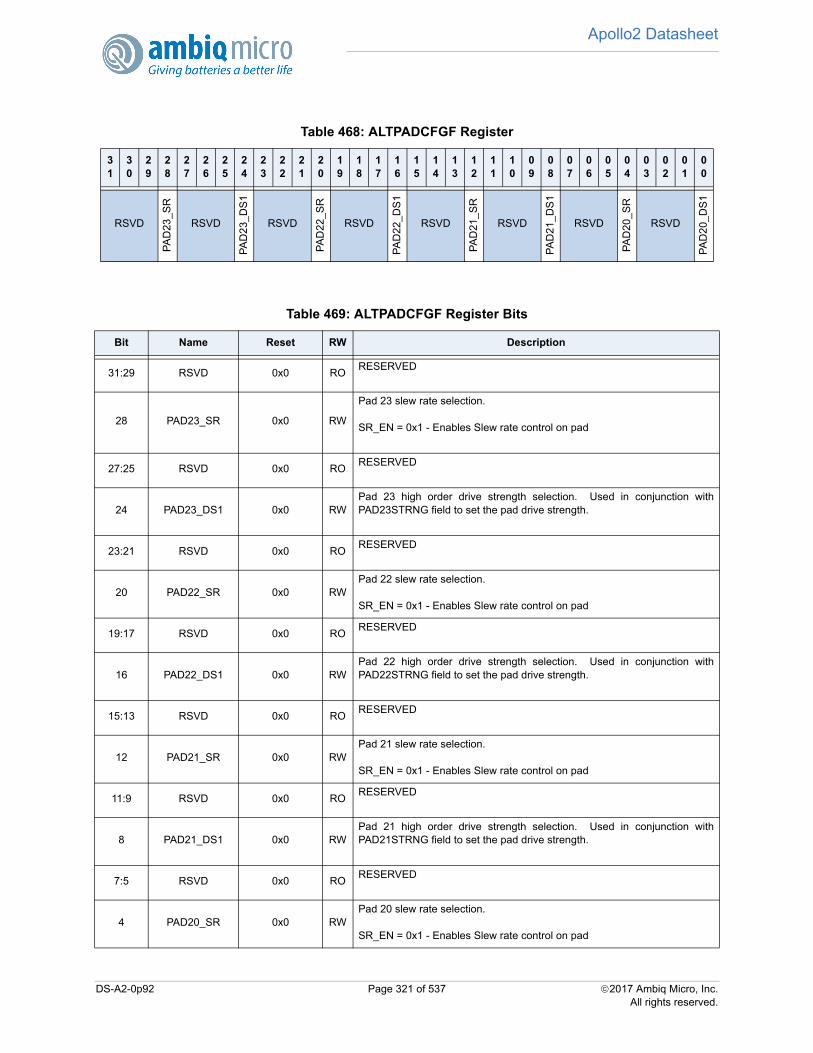
Apollo2 Datasheet
Table 468: ALTPADCFGF Register
31
30
29
28
27
26
25
24
23
22
21
20
19
18
17
16
15
14
13
12
11
10
09
08
07
06
05
04
03
02
01
00
RSVD
PA
D23
_SR
RSVD
PA
D2
3_D
S1
RSVD
PA
D22
_SR
RSVD
PA
D2
2_D
S1
RSVD
PA
D21
_SR
RSVD
PA
D2
1_D
S1
RSVD
PA
D20
_SR
RSVD
PA
D2
0_D
S1
Table 469: ALTPADCFGF Register Bits
Bit Name Reset RW Description
31:29 RSVD 0x0 RORESERVED
28 PAD23_SR 0x0 RW
Pad 23 slew rate selection.
SR_EN = 0x1 - Enables Slew rate control on pad
27:25 RSVD 0x0 RORESERVED
24 PAD23_DS1 0x0 RWPad 23 high order drive strength selection. Used in conjunction withPAD23STRNG field to set the pad drive strength.
23:21 RSVD 0x0 RORESERVED
20 PAD22_SR 0x0 RWPad 22 slew rate selection.
SR_EN = 0x1 - Enables Slew rate control on pad
19:17 RSVD 0x0 RORESERVED
16 PAD22_DS1 0x0 RWPad 22 high order drive strength selection. Used in conjunction withPAD22STRNG field to set the pad drive strength.
15:13 RSVD 0x0 RORESERVED
12 PAD21_SR 0x0 RWPad 21 slew rate selection.
SR_EN = 0x1 - Enables Slew rate control on pad
11:9 RSVD 0x0 RORESERVED
8 PAD21_DS1 0x0 RWPad 21 high order drive strength selection. Used in conjunction withPAD21STRNG field to set the pad drive strength.
7:5 RSVD 0x0 RORESERVED
4 PAD20_SR 0x0 RWPad 20 slew rate selection.
SR_EN = 0x1 - Enables Slew rate control on pad
DS-A2-0p92 Page 321 of 537 2017 Ambiq Micro, Inc.All rights reserved.
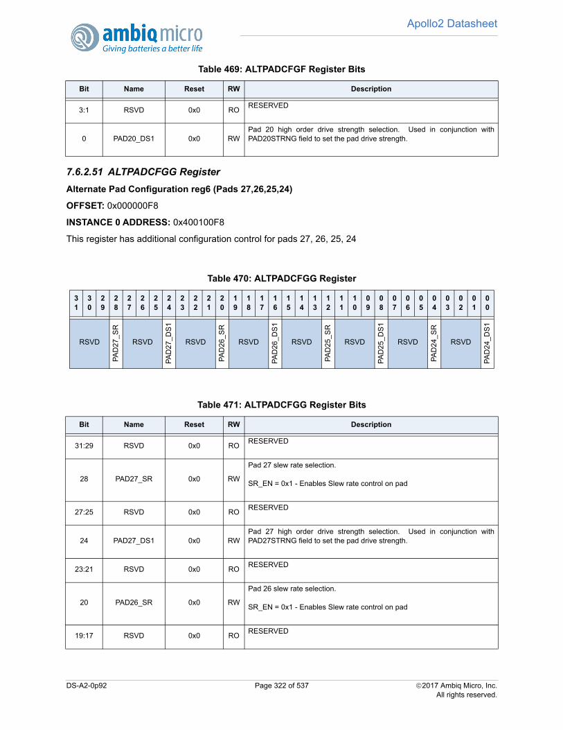
Apollo2 Datasheet
7.6.2.51 ALTPADCFGG Register
Alternate Pad Configuration reg6 (Pads 27,26,25,24)
OFFSET: 0x000000F8
INSTANCE 0 ADDRESS: 0x400100F8
This register has additional configuration control for pads 27, 26, 25, 24
3:1 RSVD 0x0 RORESERVED
0 PAD20_DS1 0x0 RWPad 20 high order drive strength selection. Used in conjunction withPAD20STRNG field to set the pad drive strength.
Table 470: ALTPADCFGG Register
31
30
29
28
27
26
25
24
23
22
21
20
19
18
17
16
15
14
13
12
11
10
09
08
07
06
05
04
03
02
01
00
RSVD
PA
D27
_SR
RSVD
PA
D27
_DS
1
RSVD
PA
D26
_SR
RSVD
PA
D26
_DS
1
RSVD
PA
D25
_SR
RSVD
PA
D25
_DS
1
RSVD
PA
D24
_SR
RSVD
PA
D24
_DS
1
Table 471: ALTPADCFGG Register Bits
Bit Name Reset RW Description
31:29 RSVD 0x0 RORESERVED
28 PAD27_SR 0x0 RW
Pad 27 slew rate selection.
SR_EN = 0x1 - Enables Slew rate control on pad
27:25 RSVD 0x0 RORESERVED
24 PAD27_DS1 0x0 RWPad 27 high order drive strength selection. Used in conjunction withPAD27STRNG field to set the pad drive strength.
23:21 RSVD 0x0 RORESERVED
20 PAD26_SR 0x0 RW
Pad 26 slew rate selection.
SR_EN = 0x1 - Enables Slew rate control on pad
19:17 RSVD 0x0 RORESERVED
Table 469: ALTPADCFGF Register Bits
Bit Name Reset RW Description
DS-A2-0p92 Page 322 of 537 2017 Ambiq Micro, Inc.All rights reserved.
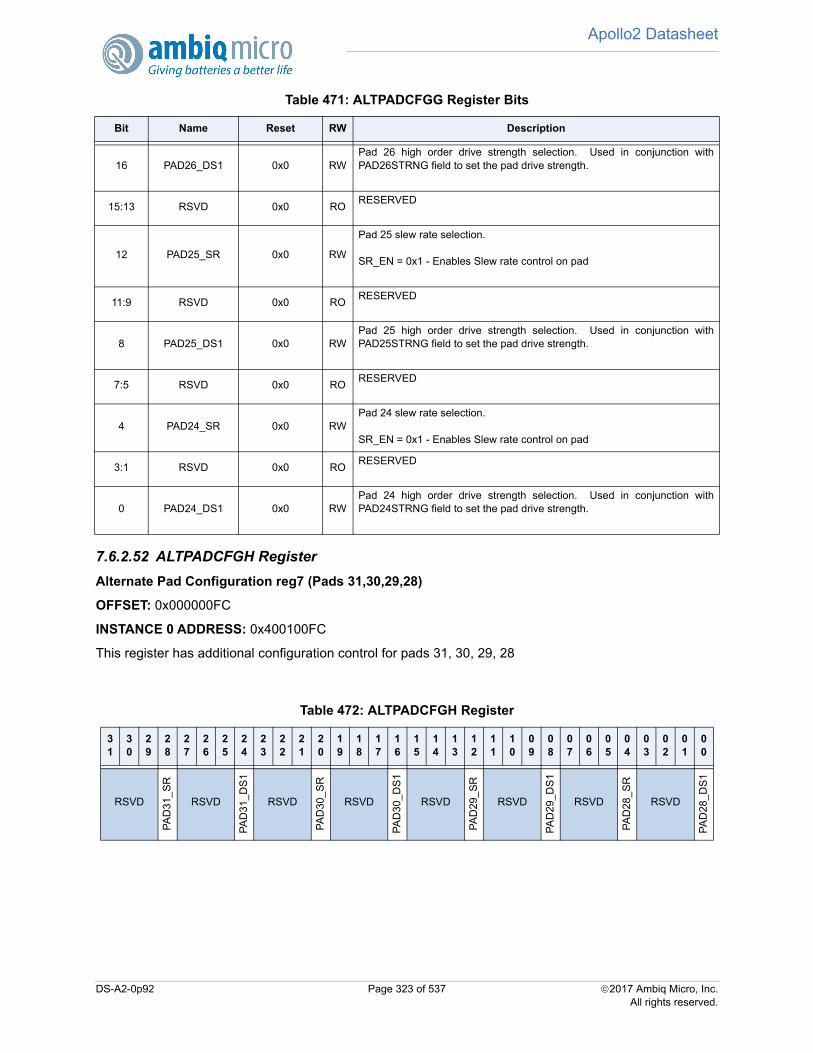
Apollo2 Datasheet
7.6.2.52 ALTPADCFGH Register
Alternate Pad Configuration reg7 (Pads 31,30,29,28)
OFFSET: 0x000000FC
INSTANCE 0 ADDRESS: 0x400100FC
This register has additional configuration control for pads 31, 30, 29, 28
16 PAD26_DS1 0x0 RWPad 26 high order drive strength selection. Used in conjunction withPAD26STRNG field to set the pad drive strength.
15:13 RSVD 0x0 RORESERVED
12 PAD25_SR 0x0 RW
Pad 25 slew rate selection.
SR_EN = 0x1 - Enables Slew rate control on pad
11:9 RSVD 0x0 RORESERVED
8 PAD25_DS1 0x0 RWPad 25 high order drive strength selection. Used in conjunction withPAD25STRNG field to set the pad drive strength.
7:5 RSVD 0x0 RORESERVED
4 PAD24_SR 0x0 RWPad 24 slew rate selection.
SR_EN = 0x1 - Enables Slew rate control on pad
3:1 RSVD 0x0 RORESERVED
0 PAD24_DS1 0x0 RWPad 24 high order drive strength selection. Used in conjunction withPAD24STRNG field to set the pad drive strength.
Table 472: ALTPADCFGH Register
31
30
29
28
27
26
25
24
23
22
21
20
19
18
17
16
15
14
13
12
11
10
09
08
07
06
05
04
03
02
01
00
RSVD
PA
D31
_S
R
RSVD
PA
D31
_DS
1
RSVD
PA
D30
_S
R
RSVD
PA
D30
_DS
1
RSVD
PA
D29
_S
R
RSVD
PA
D29
_DS
1
RSVD
PA
D28
_S
R
RSVD
PA
D28
_DS
1
Table 471: ALTPADCFGG Register Bits
Bit Name Reset RW Description
DS-A2-0p92 Page 323 of 537 2017 Ambiq Micro, Inc.All rights reserved.
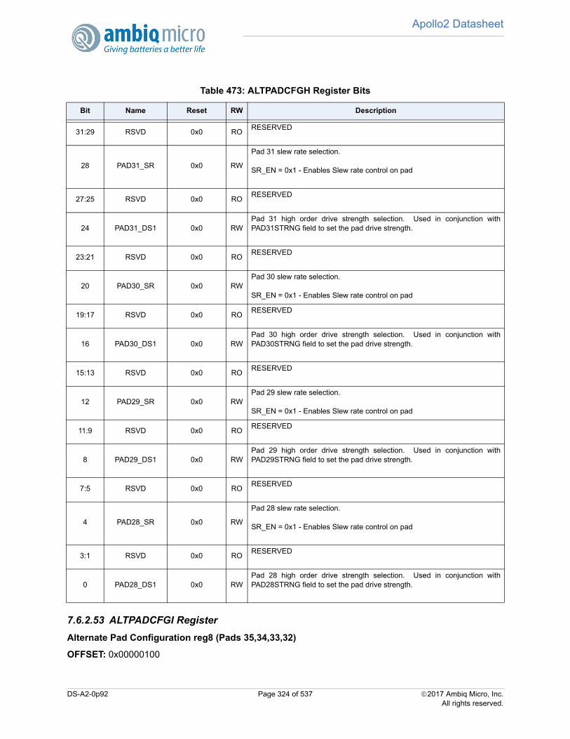
Apollo2 Datasheet
7.6.2.53 ALTPADCFGI Register
Alternate Pad Configuration reg8 (Pads 35,34,33,32)
OFFSET: 0x00000100
Table 473: ALTPADCFGH Register Bits
Bit Name Reset RW Description
31:29 RSVD 0x0 RORESERVED
28 PAD31_SR 0x0 RW
Pad 31 slew rate selection.
SR_EN = 0x1 - Enables Slew rate control on pad
27:25 RSVD 0x0 RORESERVED
24 PAD31_DS1 0x0 RWPad 31 high order drive strength selection. Used in conjunction withPAD31STRNG field to set the pad drive strength.
23:21 RSVD 0x0 RORESERVED
20 PAD30_SR 0x0 RWPad 30 slew rate selection.
SR_EN = 0x1 - Enables Slew rate control on pad
19:17 RSVD 0x0 RORESERVED
16 PAD30_DS1 0x0 RWPad 30 high order drive strength selection. Used in conjunction withPAD30STRNG field to set the pad drive strength.
15:13 RSVD 0x0 RORESERVED
12 PAD29_SR 0x0 RWPad 29 slew rate selection.
SR_EN = 0x1 - Enables Slew rate control on pad
11:9 RSVD 0x0 RORESERVED
8 PAD29_DS1 0x0 RWPad 29 high order drive strength selection. Used in conjunction withPAD29STRNG field to set the pad drive strength.
7:5 RSVD 0x0 RORESERVED
4 PAD28_SR 0x0 RW
Pad 28 slew rate selection.
SR_EN = 0x1 - Enables Slew rate control on pad
3:1 RSVD 0x0 RORESERVED
0 PAD28_DS1 0x0 RWPad 28 high order drive strength selection. Used in conjunction withPAD28STRNG field to set the pad drive strength.
DS-A2-0p92 Page 324 of 537 2017 Ambiq Micro, Inc.All rights reserved.
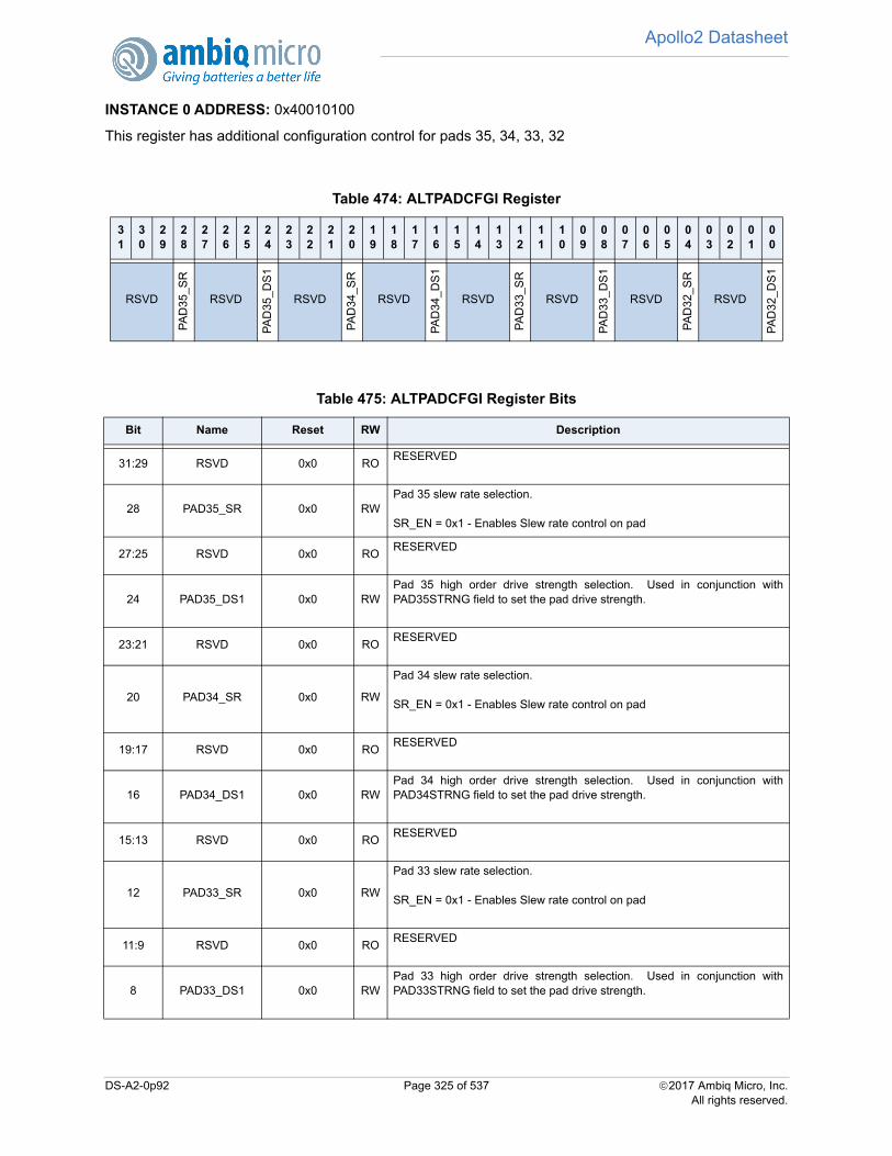
Apollo2 Datasheet
INSTANCE 0 ADDRESS: 0x40010100
This register has additional configuration control for pads 35, 34, 33, 32
Table 474: ALTPADCFGI Register
31
30
29
28
27
26
25
24
23
22
21
20
19
18
17
16
15
14
13
12
11
10
09
08
07
06
05
04
03
02
01
00
RSVD
PA
D35
_SR
RSVD
PA
D35
_DS
1
RSVD
PA
D34
_SR
RSVD
PA
D34
_DS
1
RSVD
PA
D33
_SR
RSVD
PA
D33
_DS
1
RSVD
PA
D32
_SR
RSVD
PA
D32
_DS
1
Table 475: ALTPADCFGI Register Bits
Bit Name Reset RW Description
31:29 RSVD 0x0 RORESERVED
28 PAD35_SR 0x0 RWPad 35 slew rate selection.
SR_EN = 0x1 - Enables Slew rate control on pad
27:25 RSVD 0x0 RORESERVED
24 PAD35_DS1 0x0 RWPad 35 high order drive strength selection. Used in conjunction withPAD35STRNG field to set the pad drive strength.
23:21 RSVD 0x0 RORESERVED
20 PAD34_SR 0x0 RW
Pad 34 slew rate selection.
SR_EN = 0x1 - Enables Slew rate control on pad
19:17 RSVD 0x0 RORESERVED
16 PAD34_DS1 0x0 RWPad 34 high order drive strength selection. Used in conjunction withPAD34STRNG field to set the pad drive strength.
15:13 RSVD 0x0 RORESERVED
12 PAD33_SR 0x0 RW
Pad 33 slew rate selection.
SR_EN = 0x1 - Enables Slew rate control on pad
11:9 RSVD 0x0 RORESERVED
8 PAD33_DS1 0x0 RWPad 33 high order drive strength selection. Used in conjunction withPAD33STRNG field to set the pad drive strength.
DS-A2-0p92 Page 325 of 537 2017 Ambiq Micro, Inc.All rights reserved.

Apollo2 Datasheet
7.6.2.54 ALTPADCFGJ Register
Alternate Pad Configuration reg9 (Pads 39,38,37,36)
OFFSET: 0x00000104
INSTANCE 0 ADDRESS: 0x40010104
This register has additional configuration control for pads 39, 38, 37, 36
7:5 RSVD 0x0 RORESERVED
4 PAD32_SR 0x0 RW
Pad 32 slew rate selection.
SR_EN = 0x1 - Enables Slew rate control on pad
3:1 RSVD 0x0 RORESERVED
0 PAD32_DS1 0x0 RWPad 32 high order drive strength selection. Used in conjunction withPAD32STRNG field to set the pad drive strength.
Table 476: ALTPADCFGJ Register
31
30
29
28
27
26
25
24
23
22
21
20
19
18
17
16
15
14
13
12
11
10
09
08
07
06
05
04
03
02
01
00
RSVD
PA
D39
_SR
RSVD
PA
D39
_DS
1
RSVD
PA
D38
_SR
RSVD
PA
D38
_DS
1
RSVD
PA
D37
_SR
RSVD
PA
D37
_DS
1
RSVD
PA
D36
_SR
RSVD
PA
D36
_DS
1
Table 477: ALTPADCFGJ Register Bits
Bit Name Reset RW Description
31:29 RSVD 0x0 RORESERVED
28 PAD39_SR 0x0 RWPad 39 slew rate selection.
SR_EN = 0x1 - Enables Slew rate control on pad
27:25 RSVD 0x0 RORESERVED
24 PAD39_DS1 0x0 RWPad 39 high order drive strength selection. Used in conjunction withPAD39STRNG field to set the pad drive strength.
23:21 RSVD 0x0 RORESERVED
Table 475: ALTPADCFGI Register Bits
Bit Name Reset RW Description
DS-A2-0p92 Page 326 of 537 2017 Ambiq Micro, Inc.All rights reserved.
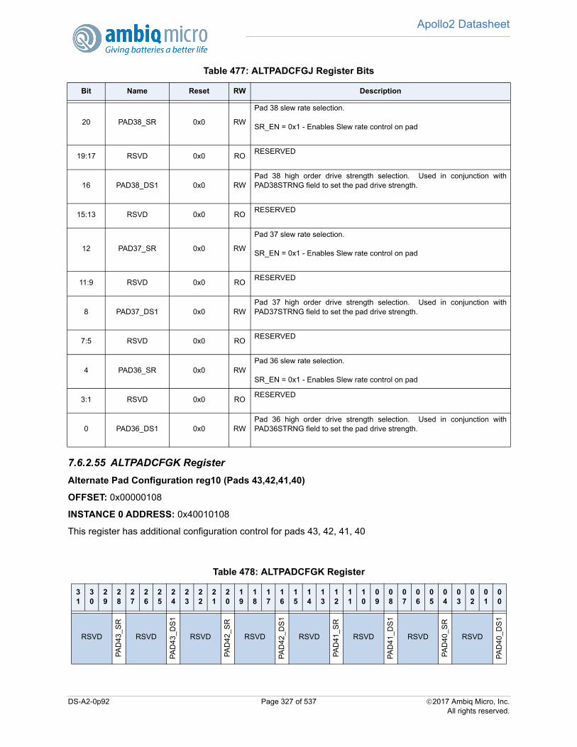
Apollo2 Datasheet
7.6.2.55 ALTPADCFGK Register
Alternate Pad Configuration reg10 (Pads 43,42,41,40)
OFFSET: 0x00000108
INSTANCE 0 ADDRESS: 0x40010108
This register has additional configuration control for pads 43, 42, 41, 40
20 PAD38_SR 0x0 RW
Pad 38 slew rate selection.
SR_EN = 0x1 - Enables Slew rate control on pad
19:17 RSVD 0x0 RORESERVED
16 PAD38_DS1 0x0 RWPad 38 high order drive strength selection. Used in conjunction withPAD38STRNG field to set the pad drive strength.
15:13 RSVD 0x0 RORESERVED
12 PAD37_SR 0x0 RW
Pad 37 slew rate selection.
SR_EN = 0x1 - Enables Slew rate control on pad
11:9 RSVD 0x0 RORESERVED
8 PAD37_DS1 0x0 RWPad 37 high order drive strength selection. Used in conjunction withPAD37STRNG field to set the pad drive strength.
7:5 RSVD 0x0 RORESERVED
4 PAD36_SR 0x0 RWPad 36 slew rate selection.
SR_EN = 0x1 - Enables Slew rate control on pad
3:1 RSVD 0x0 RORESERVED
0 PAD36_DS1 0x0 RWPad 36 high order drive strength selection. Used in conjunction withPAD36STRNG field to set the pad drive strength.
Table 478: ALTPADCFGK Register
31
30
29
28
27
26
25
24
23
22
21
20
19
18
17
16
15
14
13
12
11
10
09
08
07
06
05
04
03
02
01
00
RSVD
PA
D43
_SR
RSVD
PA
D43
_DS
1
RSVD
PA
D42
_SR
RSVD
PA
D42
_DS
1
RSVD
PA
D41
_SR
RSVD
PA
D41
_DS
1
RSVD
PA
D40
_SR
RSVD
PA
D40
_DS
1
Table 477: ALTPADCFGJ Register Bits
Bit Name Reset RW Description
DS-A2-0p92 Page 327 of 537 2017 Ambiq Micro, Inc.All rights reserved.
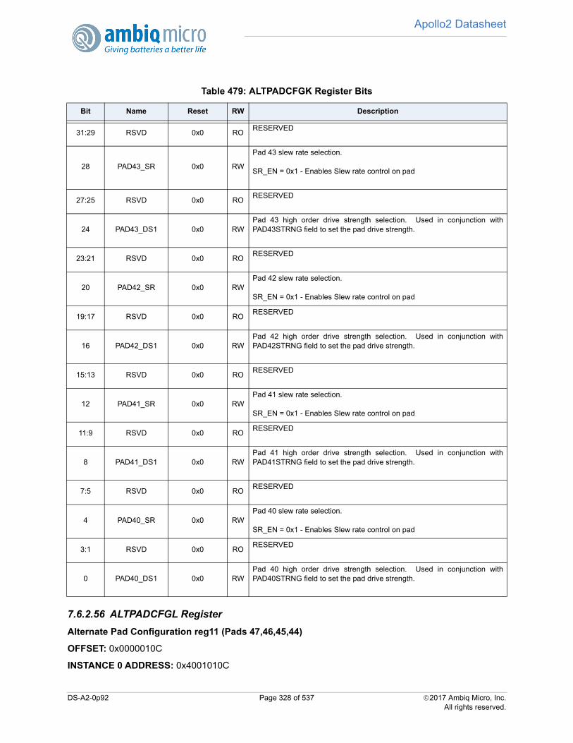
Apollo2 Datasheet
7.6.2.56 ALTPADCFGL Register
Alternate Pad Configuration reg11 (Pads 47,46,45,44)
OFFSET: 0x0000010C
INSTANCE 0 ADDRESS: 0x4001010C
Table 479: ALTPADCFGK Register Bits
Bit Name Reset RW Description
31:29 RSVD 0x0 RORESERVED
28 PAD43_SR 0x0 RW
Pad 43 slew rate selection.
SR_EN = 0x1 - Enables Slew rate control on pad
27:25 RSVD 0x0 RORESERVED
24 PAD43_DS1 0x0 RWPad 43 high order drive strength selection. Used in conjunction withPAD43STRNG field to set the pad drive strength.
23:21 RSVD 0x0 RORESERVED
20 PAD42_SR 0x0 RWPad 42 slew rate selection.
SR_EN = 0x1 - Enables Slew rate control on pad
19:17 RSVD 0x0 RORESERVED
16 PAD42_DS1 0x0 RWPad 42 high order drive strength selection. Used in conjunction withPAD42STRNG field to set the pad drive strength.
15:13 RSVD 0x0 RORESERVED
12 PAD41_SR 0x0 RWPad 41 slew rate selection.
SR_EN = 0x1 - Enables Slew rate control on pad
11:9 RSVD 0x0 RORESERVED
8 PAD41_DS1 0x0 RWPad 41 high order drive strength selection. Used in conjunction withPAD41STRNG field to set the pad drive strength.
7:5 RSVD 0x0 RORESERVED
4 PAD40_SR 0x0 RWPad 40 slew rate selection.
SR_EN = 0x1 - Enables Slew rate control on pad
3:1 RSVD 0x0 RORESERVED
0 PAD40_DS1 0x0 RWPad 40 high order drive strength selection. Used in conjunction withPAD40STRNG field to set the pad drive strength.
DS-A2-0p92 Page 328 of 537 2017 Ambiq Micro, Inc.All rights reserved.
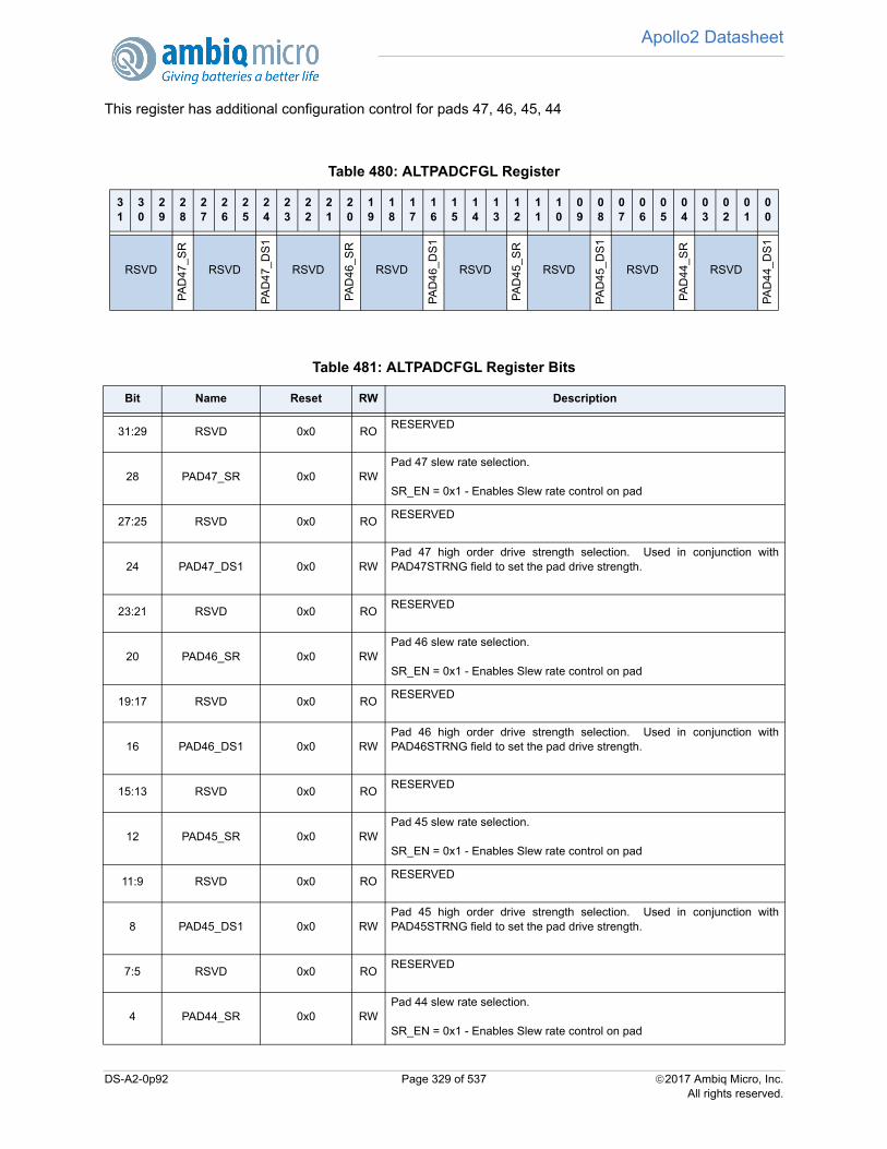
Apollo2 Datasheet
This register has additional configuration control for pads 47, 46, 45, 44
Table 480: ALTPADCFGL Register
31
30
29
28
27
26
25
24
23
22
21
20
19
18
17
16
15
14
13
12
11
10
09
08
07
06
05
04
03
02
01
00
RSVD
PA
D47
_SR
RSVDP
AD
47_
DS
1RSVD
PA
D46
_SR
RSVD
PA
D4
6_D
S1
RSVD
PA
D45
_SR
RSVD
PA
D4
5_D
S1
RSVD
PA
D44
_SR
RSVD
PA
D4
4_D
S1
Table 481: ALTPADCFGL Register Bits
Bit Name Reset RW Description
31:29 RSVD 0x0 RORESERVED
28 PAD47_SR 0x0 RWPad 47 slew rate selection.
SR_EN = 0x1 - Enables Slew rate control on pad
27:25 RSVD 0x0 RORESERVED
24 PAD47_DS1 0x0 RWPad 47 high order drive strength selection. Used in conjunction withPAD47STRNG field to set the pad drive strength.
23:21 RSVD 0x0 RORESERVED
20 PAD46_SR 0x0 RWPad 46 slew rate selection.
SR_EN = 0x1 - Enables Slew rate control on pad
19:17 RSVD 0x0 RORESERVED
16 PAD46_DS1 0x0 RWPad 46 high order drive strength selection. Used in conjunction withPAD46STRNG field to set the pad drive strength.
15:13 RSVD 0x0 RORESERVED
12 PAD45_SR 0x0 RWPad 45 slew rate selection.
SR_EN = 0x1 - Enables Slew rate control on pad
11:9 RSVD 0x0 RORESERVED
8 PAD45_DS1 0x0 RWPad 45 high order drive strength selection. Used in conjunction withPAD45STRNG field to set the pad drive strength.
7:5 RSVD 0x0 RORESERVED
4 PAD44_SR 0x0 RWPad 44 slew rate selection.
SR_EN = 0x1 - Enables Slew rate control on pad
DS-A2-0p92 Page 329 of 537 2017 Ambiq Micro, Inc.All rights reserved.
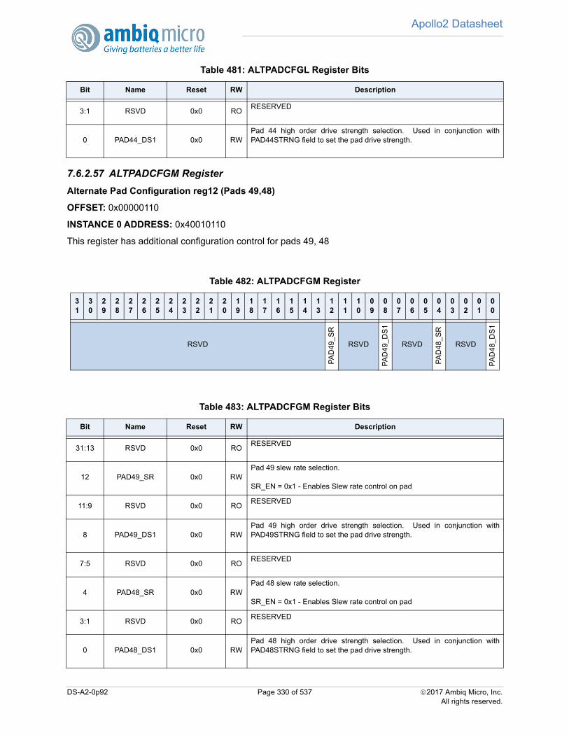
Apollo2 Datasheet
7.6.2.57 ALTPADCFGM Register
Alternate Pad Configuration reg12 (Pads 49,48)
OFFSET: 0x00000110
INSTANCE 0 ADDRESS: 0x40010110
This register has additional configuration control for pads 49, 48
3:1 RSVD 0x0 RORESERVED
0 PAD44_DS1 0x0 RWPad 44 high order drive strength selection. Used in conjunction withPAD44STRNG field to set the pad drive strength.
Table 482: ALTPADCFGM Register
31
30
29
28
27
26
25
24
23
22
21
20
19
18
17
16
15
14
13
12
11
10
09
08
07
06
05
04
03
02
01
00
RSVD
PA
D49
_SR
RSVD
PA
D49
_DS
1
RSVD
PA
D48
_SR
RSVD
PA
D48
_DS
1
Table 483: ALTPADCFGM Register Bits
Bit Name Reset RW Description
31:13 RSVD 0x0 RORESERVED
12 PAD49_SR 0x0 RWPad 49 slew rate selection.
SR_EN = 0x1 - Enables Slew rate control on pad
11:9 RSVD 0x0 RORESERVED
8 PAD49_DS1 0x0 RWPad 49 high order drive strength selection. Used in conjunction withPAD49STRNG field to set the pad drive strength.
7:5 RSVD 0x0 RORESERVED
4 PAD48_SR 0x0 RWPad 48 slew rate selection.
SR_EN = 0x1 - Enables Slew rate control on pad
3:1 RSVD 0x0 RORESERVED
0 PAD48_DS1 0x0 RWPad 48 high order drive strength selection. Used in conjunction withPAD48STRNG field to set the pad drive strength.
Table 481: ALTPADCFGL Register Bits
Bit Name Reset RW Description
DS-A2-0p92 Page 330 of 537 2017 Ambiq Micro, Inc.All rights reserved.
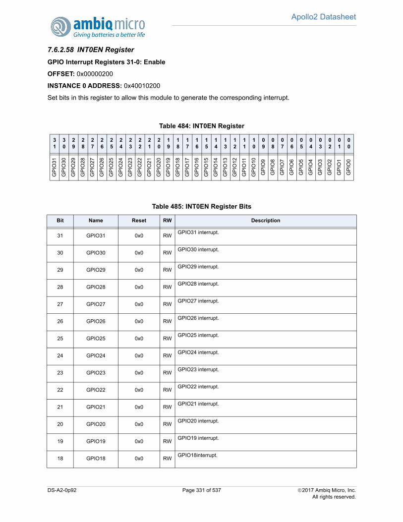
Apollo2 Datasheet
7.6.2.58 INT0EN Register
GPIO Interrupt Registers 31-0: Enable
OFFSET: 0x00000200
INSTANCE 0 ADDRESS: 0x40010200
Set bits in this register to allow this module to generate the corresponding interrupt.
Table 484: INT0EN Register
31
30
29
28
27
26
25
24
23
22
21
20
19
18
17
16
15
14
13
12
11
10
09
08
07
06
05
04
03
02
01
00
GP
IO3
1
GP
IO30
GP
IO29
GP
IO2
8
GP
IO2
7
GP
IO2
6
GP
IO2
5
GP
IO24
GP
IO2
3
GP
IO22
GP
IO21
GP
IO20
GP
IO19
GP
IO18
GP
IO17
GP
IO16
GP
IO15
GP
IO14
GP
IO13
GP
IO12
GP
IO11
GP
IO10
GP
IO9
GP
IO8
GP
IO7
GP
IO6
GP
IO5
GP
IO4
GP
IO3
GP
IO2
GP
IO1
GP
IO0
Table 485: INT0EN Register Bits
Bit Name Reset RW Description
31 GPIO31 0x0 RWGPIO31 interrupt.
30 GPIO30 0x0 RWGPIO30 interrupt.
29 GPIO29 0x0 RWGPIO29 interrupt.
28 GPIO28 0x0 RWGPIO28 interrupt.
27 GPIO27 0x0 RWGPIO27 interrupt.
26 GPIO26 0x0 RWGPIO26 interrupt.
25 GPIO25 0x0 RWGPIO25 interrupt.
24 GPIO24 0x0 RWGPIO24 interrupt.
23 GPIO23 0x0 RWGPIO23 interrupt.
22 GPIO22 0x0 RWGPIO22 interrupt.
21 GPIO21 0x0 RWGPIO21 interrupt.
20 GPIO20 0x0 RWGPIO20 interrupt.
19 GPIO19 0x0 RWGPIO19 interrupt.
18 GPIO18 0x0 RWGPIO18interrupt.
DS-A2-0p92 Page 331 of 537 2017 Ambiq Micro, Inc.All rights reserved.
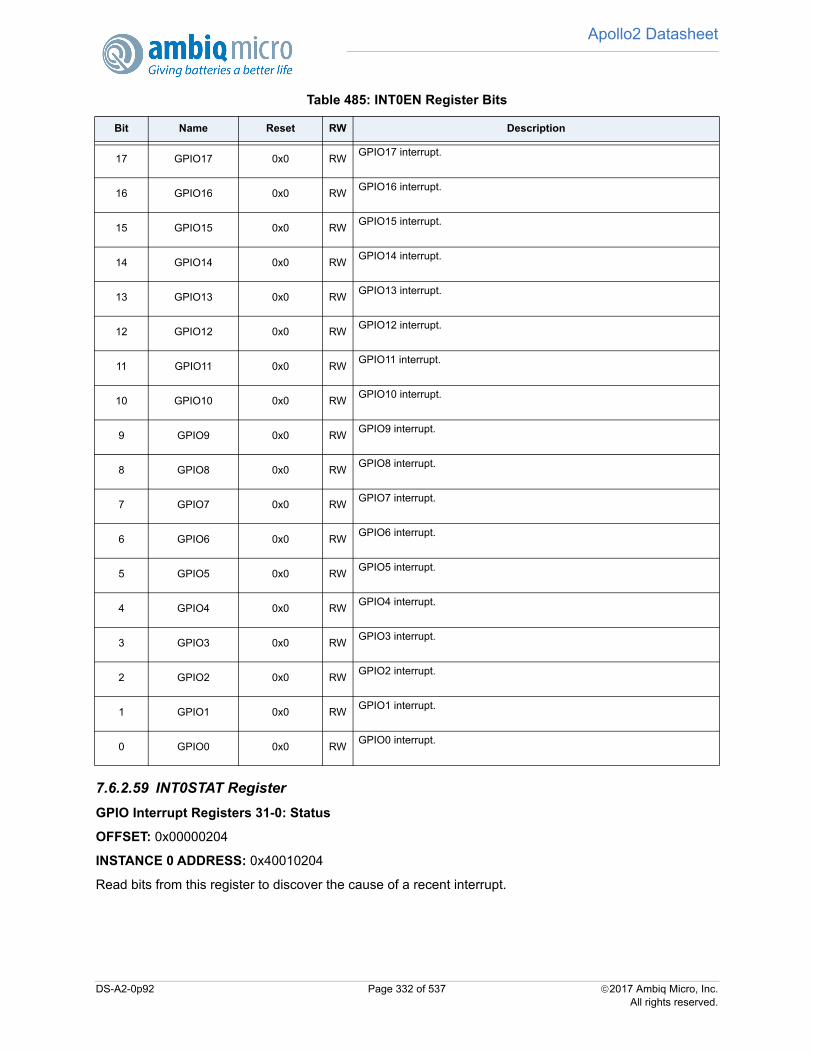
Apollo2 Datasheet
7.6.2.59 INT0STAT Register
GPIO Interrupt Registers 31-0: Status
OFFSET: 0x00000204
INSTANCE 0 ADDRESS: 0x40010204
Read bits from this register to discover the cause of a recent interrupt.
17 GPIO17 0x0 RWGPIO17 interrupt.
16 GPIO16 0x0 RWGPIO16 interrupt.
15 GPIO15 0x0 RWGPIO15 interrupt.
14 GPIO14 0x0 RWGPIO14 interrupt.
13 GPIO13 0x0 RWGPIO13 interrupt.
12 GPIO12 0x0 RWGPIO12 interrupt.
11 GPIO11 0x0 RWGPIO11 interrupt.
10 GPIO10 0x0 RWGPIO10 interrupt.
9 GPIO9 0x0 RWGPIO9 interrupt.
8 GPIO8 0x0 RWGPIO8 interrupt.
7 GPIO7 0x0 RWGPIO7 interrupt.
6 GPIO6 0x0 RWGPIO6 interrupt.
5 GPIO5 0x0 RWGPIO5 interrupt.
4 GPIO4 0x0 RWGPIO4 interrupt.
3 GPIO3 0x0 RWGPIO3 interrupt.
2 GPIO2 0x0 RWGPIO2 interrupt.
1 GPIO1 0x0 RWGPIO1 interrupt.
0 GPIO0 0x0 RWGPIO0 interrupt.
Table 485: INT0EN Register Bits
Bit Name Reset RW Description
DS-A2-0p92 Page 332 of 537 2017 Ambiq Micro, Inc.All rights reserved.
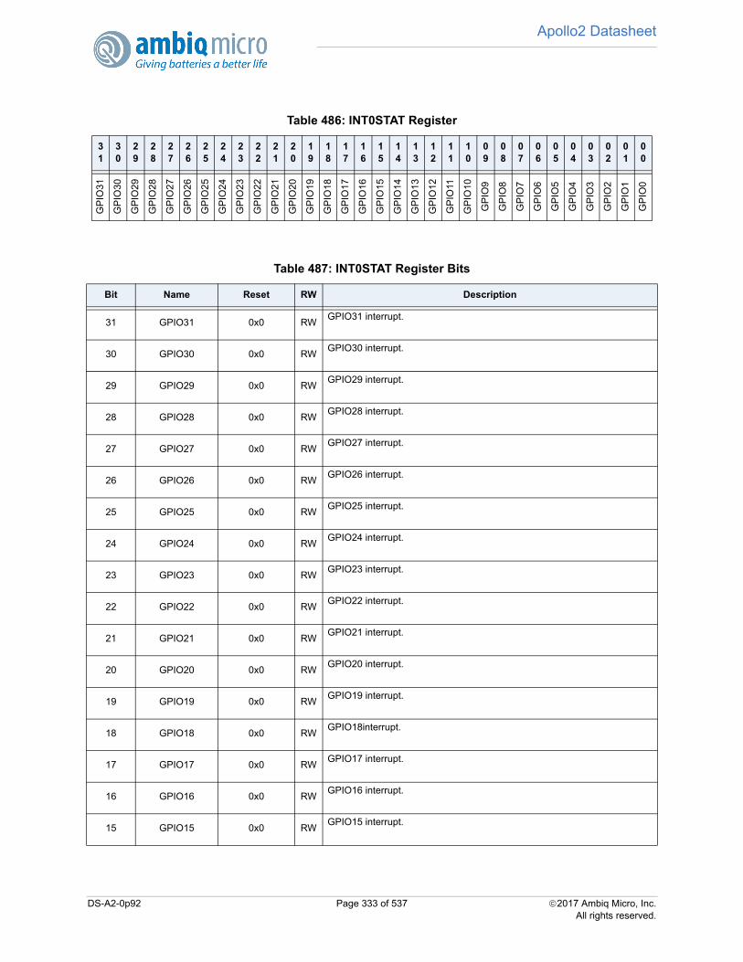
Apollo2 Datasheet
Table 486: INT0STAT Register
31
30
29
28
27
26
25
24
23
22
21
20
19
18
17
16
15
14
13
12
11
10
09
08
07
06
05
04
03
02
01
00
GP
IO31
GP
IO30
GP
IO29
GP
IO28
GP
IO27
GP
IO26
GP
IO25
GP
IO24
GP
IO23
GP
IO22
GP
IO21
GP
IO20
GP
IO19
GP
IO18
GP
IO17
GP
IO16
GP
IO15
GP
IO14
GP
IO13
GP
IO12
GP
IO11
GP
IO10
GP
IO9
GP
IO8
GP
IO7
GP
IO6
GP
IO5
GP
IO4
GP
IO3
GP
IO2
GP
IO1
GP
IO0
Table 487: INT0STAT Register Bits
Bit Name Reset RW Description
31 GPIO31 0x0 RWGPIO31 interrupt.
30 GPIO30 0x0 RWGPIO30 interrupt.
29 GPIO29 0x0 RWGPIO29 interrupt.
28 GPIO28 0x0 RWGPIO28 interrupt.
27 GPIO27 0x0 RWGPIO27 interrupt.
26 GPIO26 0x0 RWGPIO26 interrupt.
25 GPIO25 0x0 RWGPIO25 interrupt.
24 GPIO24 0x0 RWGPIO24 interrupt.
23 GPIO23 0x0 RWGPIO23 interrupt.
22 GPIO22 0x0 RWGPIO22 interrupt.
21 GPIO21 0x0 RWGPIO21 interrupt.
20 GPIO20 0x0 RWGPIO20 interrupt.
19 GPIO19 0x0 RWGPIO19 interrupt.
18 GPIO18 0x0 RWGPIO18interrupt.
17 GPIO17 0x0 RWGPIO17 interrupt.
16 GPIO16 0x0 RWGPIO16 interrupt.
15 GPIO15 0x0 RWGPIO15 interrupt.
DS-A2-0p92 Page 333 of 537 2017 Ambiq Micro, Inc.All rights reserved.
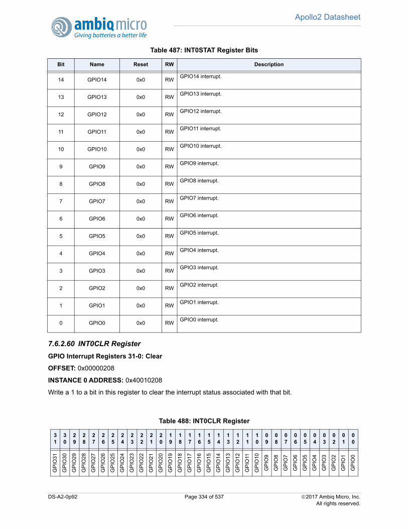
Apollo2 Datasheet
7.6.2.60 INT0CLR Register
GPIO Interrupt Registers 31-0: Clear
OFFSET: 0x00000208
INSTANCE 0 ADDRESS: 0x40010208
Write a 1 to a bit in this register to clear the interrupt status associated with that bit.
14 GPIO14 0x0 RWGPIO14 interrupt.
13 GPIO13 0x0 RWGPIO13 interrupt.
12 GPIO12 0x0 RWGPIO12 interrupt.
11 GPIO11 0x0 RWGPIO11 interrupt.
10 GPIO10 0x0 RWGPIO10 interrupt.
9 GPIO9 0x0 RWGPIO9 interrupt.
8 GPIO8 0x0 RWGPIO8 interrupt.
7 GPIO7 0x0 RWGPIO7 interrupt.
6 GPIO6 0x0 RWGPIO6 interrupt.
5 GPIO5 0x0 RWGPIO5 interrupt.
4 GPIO4 0x0 RWGPIO4 interrupt.
3 GPIO3 0x0 RWGPIO3 interrupt.
2 GPIO2 0x0 RWGPIO2 interrupt.
1 GPIO1 0x0 RWGPIO1 interrupt.
0 GPIO0 0x0 RWGPIO0 interrupt.
Table 488: INT0CLR Register
31
30
29
28
27
26
25
24
23
22
21
20
19
18
17
16
15
14
13
12
11
10
09
08
07
06
05
04
03
02
01
00
GP
IO3
1
GP
IO30
GP
IO29
GP
IO2
8
GP
IO2
7
GP
IO2
6
GP
IO2
5
GP
IO24
GP
IO2
3
GP
IO22
GP
IO21
GP
IO20
GP
IO19
GP
IO18
GP
IO17
GP
IO16
GP
IO15
GP
IO14
GP
IO13
GP
IO12
GP
IO11
GP
IO10
GP
IO9
GP
IO8
GP
IO7
GP
IO6
GP
IO5
GP
IO4
GP
IO3
GP
IO2
GP
IO1
GP
IO0
Table 487: INT0STAT Register Bits
Bit Name Reset RW Description
DS-A2-0p92 Page 334 of 537 2017 Ambiq Micro, Inc.All rights reserved.
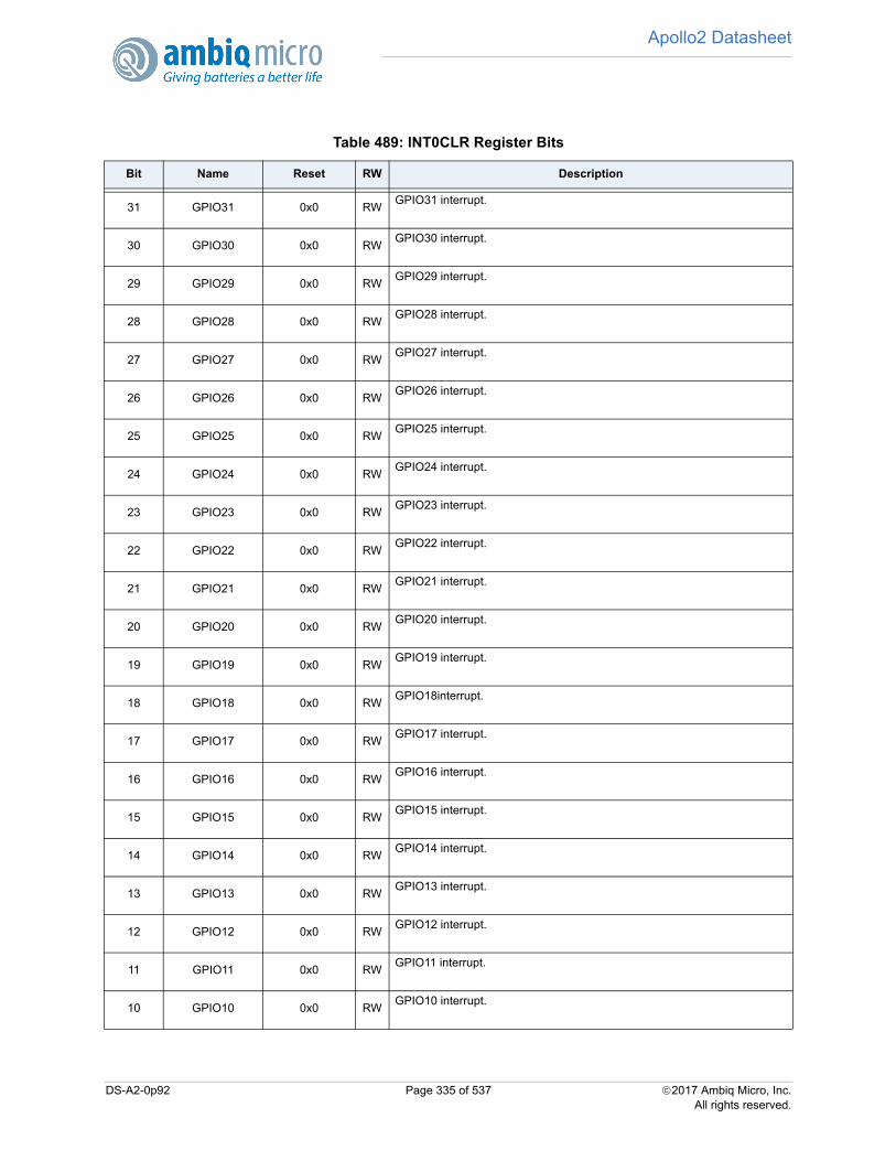
Apollo2 Datasheet
Table 489: INT0CLR Register Bits
Bit Name Reset RW Description
31 GPIO31 0x0 RWGPIO31 interrupt.
30 GPIO30 0x0 RWGPIO30 interrupt.
29 GPIO29 0x0 RWGPIO29 interrupt.
28 GPIO28 0x0 RWGPIO28 interrupt.
27 GPIO27 0x0 RWGPIO27 interrupt.
26 GPIO26 0x0 RWGPIO26 interrupt.
25 GPIO25 0x0 RWGPIO25 interrupt.
24 GPIO24 0x0 RWGPIO24 interrupt.
23 GPIO23 0x0 RWGPIO23 interrupt.
22 GPIO22 0x0 RWGPIO22 interrupt.
21 GPIO21 0x0 RWGPIO21 interrupt.
20 GPIO20 0x0 RWGPIO20 interrupt.
19 GPIO19 0x0 RWGPIO19 interrupt.
18 GPIO18 0x0 RWGPIO18interrupt.
17 GPIO17 0x0 RWGPIO17 interrupt.
16 GPIO16 0x0 RWGPIO16 interrupt.
15 GPIO15 0x0 RWGPIO15 interrupt.
14 GPIO14 0x0 RWGPIO14 interrupt.
13 GPIO13 0x0 RWGPIO13 interrupt.
12 GPIO12 0x0 RWGPIO12 interrupt.
11 GPIO11 0x0 RWGPIO11 interrupt.
10 GPIO10 0x0 RWGPIO10 interrupt.
DS-A2-0p92 Page 335 of 537 2017 Ambiq Micro, Inc.All rights reserved.

Apollo2 Datasheet
7.6.2.61 INT0SET Register
GPIO Interrupt Registers 31-0: Set
OFFSET: 0x0000020C
INSTANCE 0 ADDRESS: 0x4001020C
Write a 1 to a bit in this register to instantly generate an interrupt from this module. (Generally used fortesting purposes).
9 GPIO9 0x0 RWGPIO9 interrupt.
8 GPIO8 0x0 RWGPIO8 interrupt.
7 GPIO7 0x0 RWGPIO7 interrupt.
6 GPIO6 0x0 RWGPIO6 interrupt.
5 GPIO5 0x0 RWGPIO5 interrupt.
4 GPIO4 0x0 RWGPIO4 interrupt.
3 GPIO3 0x0 RWGPIO3 interrupt.
2 GPIO2 0x0 RWGPIO2 interrupt.
1 GPIO1 0x0 RWGPIO1 interrupt.
0 GPIO0 0x0 RWGPIO0 interrupt.
Table 490: INT0SET Register
31
30
29
28
27
26
25
24
23
22
21
20
19
18
17
16
15
14
13
12
11
10
09
08
07
06
05
04
03
02
01
00
GP
IO31
GP
IO30
GP
IO29
GP
IO28
GP
IO27
GP
IO26
GP
IO25
GP
IO24
GP
IO23
GP
IO22
GP
IO21
GP
IO20
GP
IO19
GP
IO18
GP
IO17
GP
IO16
GP
IO15
GP
IO14
GP
IO13
GP
IO12
GP
IO11
GP
IO10
GP
IO9
GP
IO8
GP
IO7
GP
IO6
GP
IO5
GP
IO4
GP
IO3
GP
IO2
GP
IO1
GP
IO0
Table 491: INT0SET Register Bits
Bit Name Reset RW Description
31 GPIO31 0x0 RWGPIO31 interrupt.
30 GPIO30 0x0 RWGPIO30 interrupt.
Table 489: INT0CLR Register Bits
Bit Name Reset RW Description
DS-A2-0p92 Page 336 of 537 2017 Ambiq Micro, Inc.All rights reserved.
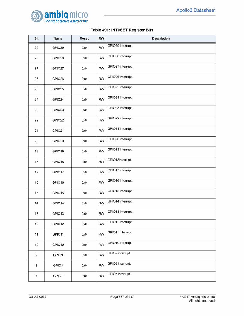
Apollo2 Datasheet
29 GPIO29 0x0 RWGPIO29 interrupt.
28 GPIO28 0x0 RWGPIO28 interrupt.
27 GPIO27 0x0 RWGPIO27 interrupt.
26 GPIO26 0x0 RWGPIO26 interrupt.
25 GPIO25 0x0 RWGPIO25 interrupt.
24 GPIO24 0x0 RWGPIO24 interrupt.
23 GPIO23 0x0 RWGPIO23 interrupt.
22 GPIO22 0x0 RWGPIO22 interrupt.
21 GPIO21 0x0 RWGPIO21 interrupt.
20 GPIO20 0x0 RWGPIO20 interrupt.
19 GPIO19 0x0 RWGPIO19 interrupt.
18 GPIO18 0x0 RWGPIO18interrupt.
17 GPIO17 0x0 RWGPIO17 interrupt.
16 GPIO16 0x0 RWGPIO16 interrupt.
15 GPIO15 0x0 RWGPIO15 interrupt.
14 GPIO14 0x0 RWGPIO14 interrupt.
13 GPIO13 0x0 RWGPIO13 interrupt.
12 GPIO12 0x0 RWGPIO12 interrupt.
11 GPIO11 0x0 RWGPIO11 interrupt.
10 GPIO10 0x0 RWGPIO10 interrupt.
9 GPIO9 0x0 RWGPIO9 interrupt.
8 GPIO8 0x0 RWGPIO8 interrupt.
7 GPIO7 0x0 RWGPIO7 interrupt.
Table 491: INT0SET Register Bits
Bit Name Reset RW Description
DS-A2-0p92 Page 337 of 537 2017 Ambiq Micro, Inc.All rights reserved.
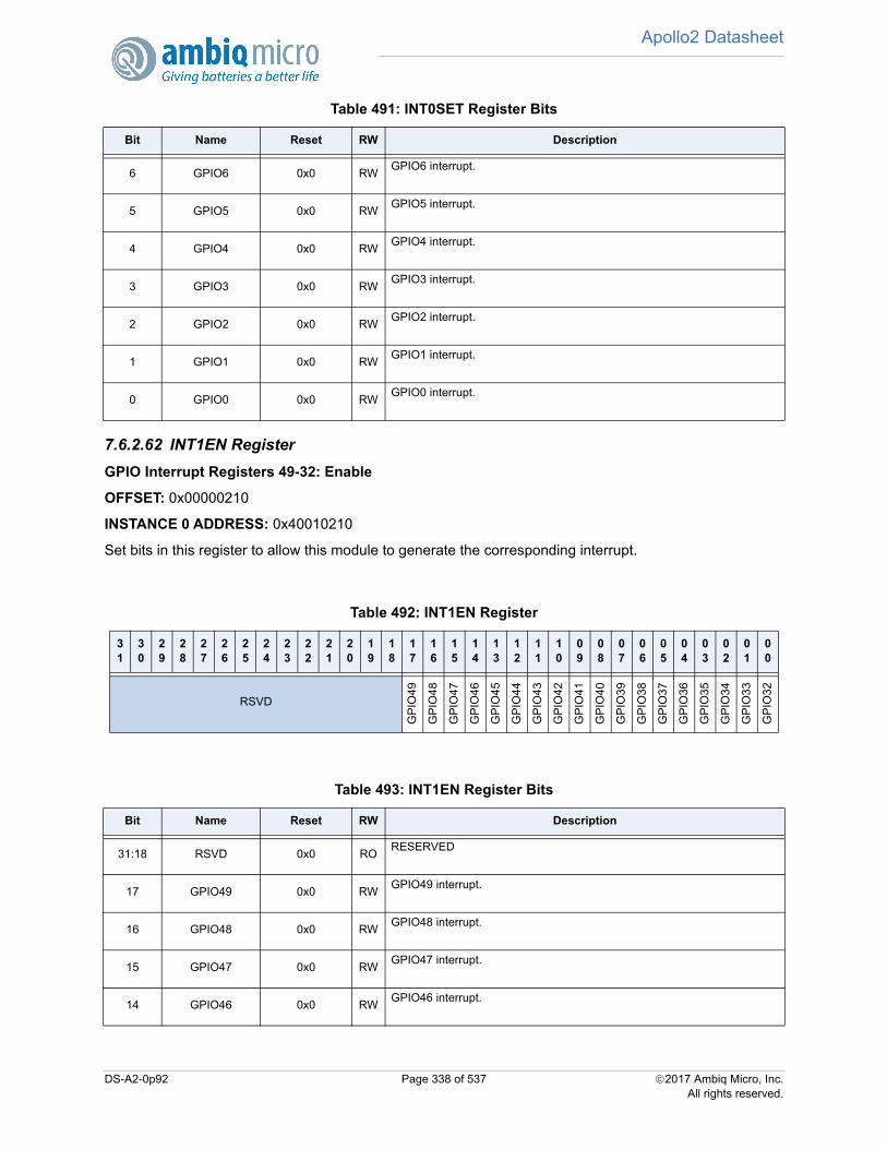
Apollo2 Datasheet
7.6.2.62 INT1EN Register
GPIO Interrupt Registers 49-32: Enable
OFFSET: 0x00000210
INSTANCE 0 ADDRESS: 0x40010210
Set bits in this register to allow this module to generate the corresponding interrupt.
6 GPIO6 0x0 RWGPIO6 interrupt.
5 GPIO5 0x0 RWGPIO5 interrupt.
4 GPIO4 0x0 RWGPIO4 interrupt.
3 GPIO3 0x0 RWGPIO3 interrupt.
2 GPIO2 0x0 RWGPIO2 interrupt.
1 GPIO1 0x0 RWGPIO1 interrupt.
0 GPIO0 0x0 RWGPIO0 interrupt.
Table 492: INT1EN Register
31
30
29
28
27
26
25
24
23
22
21
20
19
18
17
16
15
14
13
12
11
10
09
08
07
06
05
04
03
02
01
00
RSVD
GP
IO4
9
GP
IO4
8
GP
IO4
7
GP
IO4
6
GP
IO4
5
GP
IO4
4
GP
IO43
GP
IO4
2
GP
IO4
1
GP
IO4
0
GP
IO3
9
GP
IO38
GP
IO37
GP
IO3
6
GP
IO3
5
GP
IO34
GP
IO33
GP
IO32
Table 493: INT1EN Register Bits
Bit Name Reset RW Description
31:18 RSVD 0x0 RORESERVED
17 GPIO49 0x0 RWGPIO49 interrupt.
16 GPIO48 0x0 RWGPIO48 interrupt.
15 GPIO47 0x0 RWGPIO47 interrupt.
14 GPIO46 0x0 RWGPIO46 interrupt.
Table 491: INT0SET Register Bits
Bit Name Reset RW Description
DS-A2-0p92 Page 338 of 537 2017 Ambiq Micro, Inc.All rights reserved.

Apollo2 Datasheet
7.6.2.63 INT1STAT Register
GPIO Interrupt Registers 49-32: Status
OFFSET: 0x00000214
INSTANCE 0 ADDRESS: 0x40010214
Read bits from this register to discover the cause of a recent interrupt.
13 GPIO45 0x0 RWGPIO45 interrupt.
12 GPIO44 0x0 RWGPIO44 interrupt.
11 GPIO43 0x0 RWGPIO43 interrupt.
10 GPIO42 0x0 RWGPIO42 interrupt.
9 GPIO41 0x0 RWGPIO41 interrupt.
8 GPIO40 0x0 RWGPIO40 interrupt.
7 GPIO39 0x0 RWGPIO39 interrupt.
6 GPIO38 0x0 RWGPIO38 interrupt.
5 GPIO37 0x0 RWGPIO37 interrupt.
4 GPIO36 0x0 RWGPIO36 interrupt.
3 GPIO35 0x0 RWGPIO35 interrupt.
2 GPIO34 0x0 RWGPIO34 interrupt.
1 GPIO33 0x0 RWGPIO33 interrupt.
0 GPIO32 0x0 RWGPIO32 interrupt.
Table 494: INT1STAT Register
31
30
29
28
27
26
25
24
23
22
21
20
19
18
17
16
15
14
13
12
11
10
09
08
07
06
05
04
03
02
01
00
RSVD
GP
IO49
GP
IO48
GP
IO47
GP
IO46
GP
IO45
GP
IO44
GP
IO43
GP
IO42
GP
IO41
GP
IO40
GP
IO39
GP
IO38
GP
IO37
GP
IO36
GP
IO35
GP
IO34
GP
IO33
GP
IO32
Table 493: INT1EN Register Bits
Bit Name Reset RW Description
DS-A2-0p92 Page 339 of 537 2017 Ambiq Micro, Inc.All rights reserved.
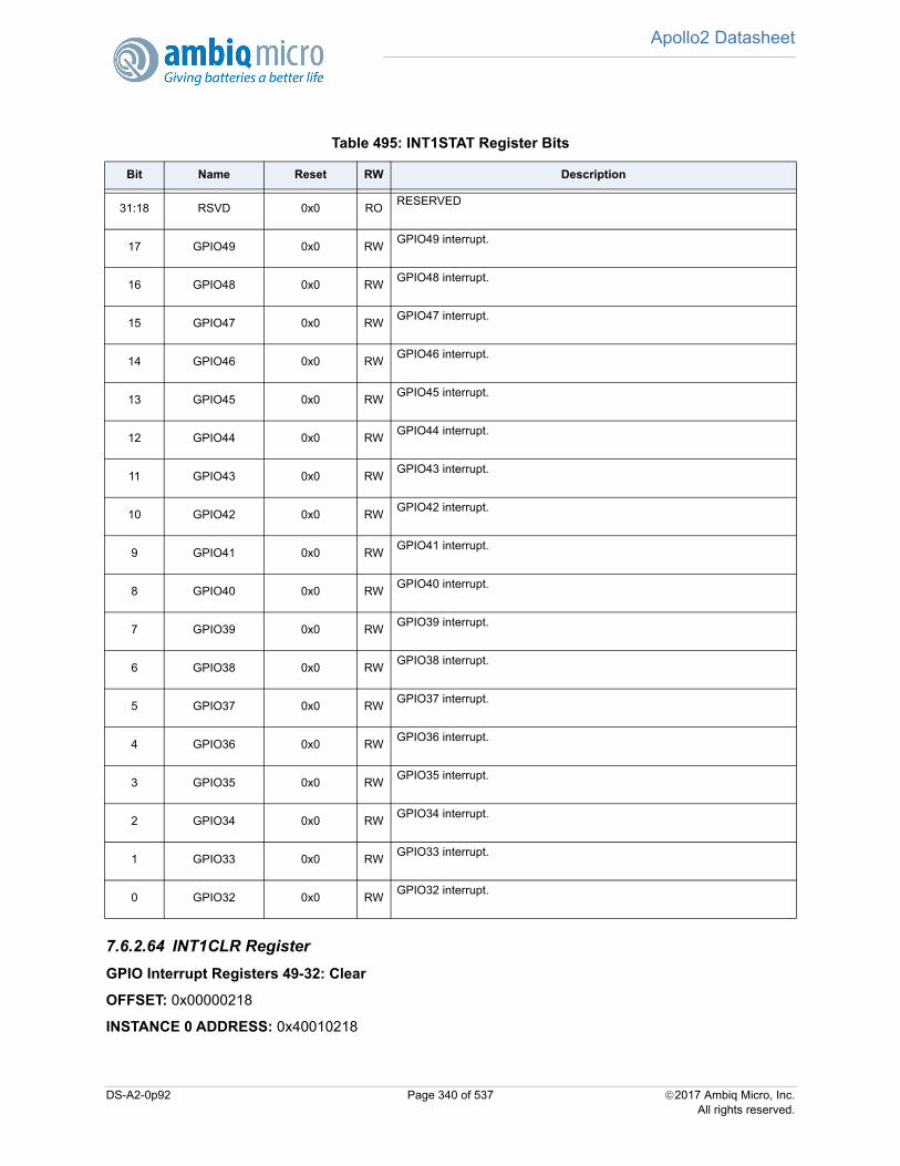
Apollo2 Datasheet
7.6.2.64 INT1CLR Register
GPIO Interrupt Registers 49-32: Clear
OFFSET: 0x00000218
INSTANCE 0 ADDRESS: 0x40010218
Table 495: INT1STAT Register Bits
Bit Name Reset RW Description
31:18 RSVD 0x0 RORESERVED
17 GPIO49 0x0 RWGPIO49 interrupt.
16 GPIO48 0x0 RWGPIO48 interrupt.
15 GPIO47 0x0 RWGPIO47 interrupt.
14 GPIO46 0x0 RWGPIO46 interrupt.
13 GPIO45 0x0 RWGPIO45 interrupt.
12 GPIO44 0x0 RWGPIO44 interrupt.
11 GPIO43 0x0 RWGPIO43 interrupt.
10 GPIO42 0x0 RWGPIO42 interrupt.
9 GPIO41 0x0 RWGPIO41 interrupt.
8 GPIO40 0x0 RWGPIO40 interrupt.
7 GPIO39 0x0 RWGPIO39 interrupt.
6 GPIO38 0x0 RWGPIO38 interrupt.
5 GPIO37 0x0 RWGPIO37 interrupt.
4 GPIO36 0x0 RWGPIO36 interrupt.
3 GPIO35 0x0 RWGPIO35 interrupt.
2 GPIO34 0x0 RWGPIO34 interrupt.
1 GPIO33 0x0 RWGPIO33 interrupt.
0 GPIO32 0x0 RWGPIO32 interrupt.
DS-A2-0p92 Page 340 of 537 2017 Ambiq Micro, Inc.All rights reserved.
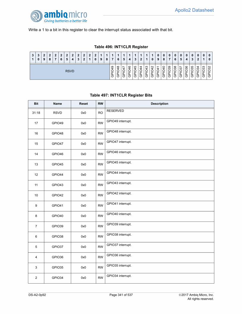
Apollo2 Datasheet
Write a 1 to a bit in this register to clear the interrupt status associated with that bit.
Table 496: INT1CLR Register
31
30
29
28
27
26
25
24
23
22
21
20
19
18
17
16
15
14
13
12
11
10
09
08
07
06
05
04
03
02
01
00
RSVD
GP
IO49
GP
IO48
GP
IO47
GP
IO46
GP
IO45
GP
IO44
GP
IO43
GP
IO42
GP
IO41
GP
IO40
GP
IO39
GP
IO38
GP
IO37
GP
IO36
GP
IO35
GP
IO34
GP
IO33
GP
IO32
Table 497: INT1CLR Register Bits
Bit Name Reset RW Description
31:18 RSVD 0x0 RORESERVED
17 GPIO49 0x0 RWGPIO49 interrupt.
16 GPIO48 0x0 RWGPIO48 interrupt.
15 GPIO47 0x0 RWGPIO47 interrupt.
14 GPIO46 0x0 RWGPIO46 interrupt.
13 GPIO45 0x0 RWGPIO45 interrupt.
12 GPIO44 0x0 RWGPIO44 interrupt.
11 GPIO43 0x0 RWGPIO43 interrupt.
10 GPIO42 0x0 RWGPIO42 interrupt.
9 GPIO41 0x0 RWGPIO41 interrupt.
8 GPIO40 0x0 RWGPIO40 interrupt.
7 GPIO39 0x0 RWGPIO39 interrupt.
6 GPIO38 0x0 RWGPIO38 interrupt.
5 GPIO37 0x0 RWGPIO37 interrupt.
4 GPIO36 0x0 RWGPIO36 interrupt.
3 GPIO35 0x0 RWGPIO35 interrupt.
2 GPIO34 0x0 RWGPIO34 interrupt.
DS-A2-0p92 Page 341 of 537 2017 Ambiq Micro, Inc.All rights reserved.

Apollo2 Datasheet
7.6.2.65 INT1SET Register
GPIO Interrupt Registers 49-32: Set
OFFSET: 0x0000021C
INSTANCE 0 ADDRESS: 0x4001021C
Write a 1 to a bit in this register to instantly generate an interrupt from this module. (Generally used fortesting purposes).
1 GPIO33 0x0 RWGPIO33 interrupt.
0 GPIO32 0x0 RWGPIO32 interrupt.
Table 498: INT1SET Register
31
30
29
28
27
26
25
24
23
22
21
20
19
18
17
16
15
14
13
12
11
10
09
08
07
06
05
04
03
02
01
00
RSVD
GP
IO49
GP
IO48
GP
IO47
GP
IO46
GP
IO45
GP
IO44
GP
IO43
GP
IO42
GP
IO41
GP
IO40
GP
IO39
GP
IO38
GP
IO37
GP
IO36
GP
IO35
GP
IO34
GP
IO33
GP
IO32
Table 499: INT1SET Register Bits
Bit Name Reset RW Description
31:18 RSVD 0x0 RORESERVED
17 GPIO49 0x0 RWGPIO49 interrupt.
16 GPIO48 0x0 RWGPIO48 interrupt.
15 GPIO47 0x0 RWGPIO47 interrupt.
14 GPIO46 0x0 RWGPIO46 interrupt.
13 GPIO45 0x0 RWGPIO45 interrupt.
12 GPIO44 0x0 RWGPIO44 interrupt.
11 GPIO43 0x0 RWGPIO43 interrupt.
10 GPIO42 0x0 RWGPIO42 interrupt.
9 GPIO41 0x0 RWGPIO41 interrupt.
Table 497: INT1CLR Register Bits
Bit Name Reset RW Description
DS-A2-0p92 Page 342 of 537 2017 Ambiq Micro, Inc.All rights reserved.
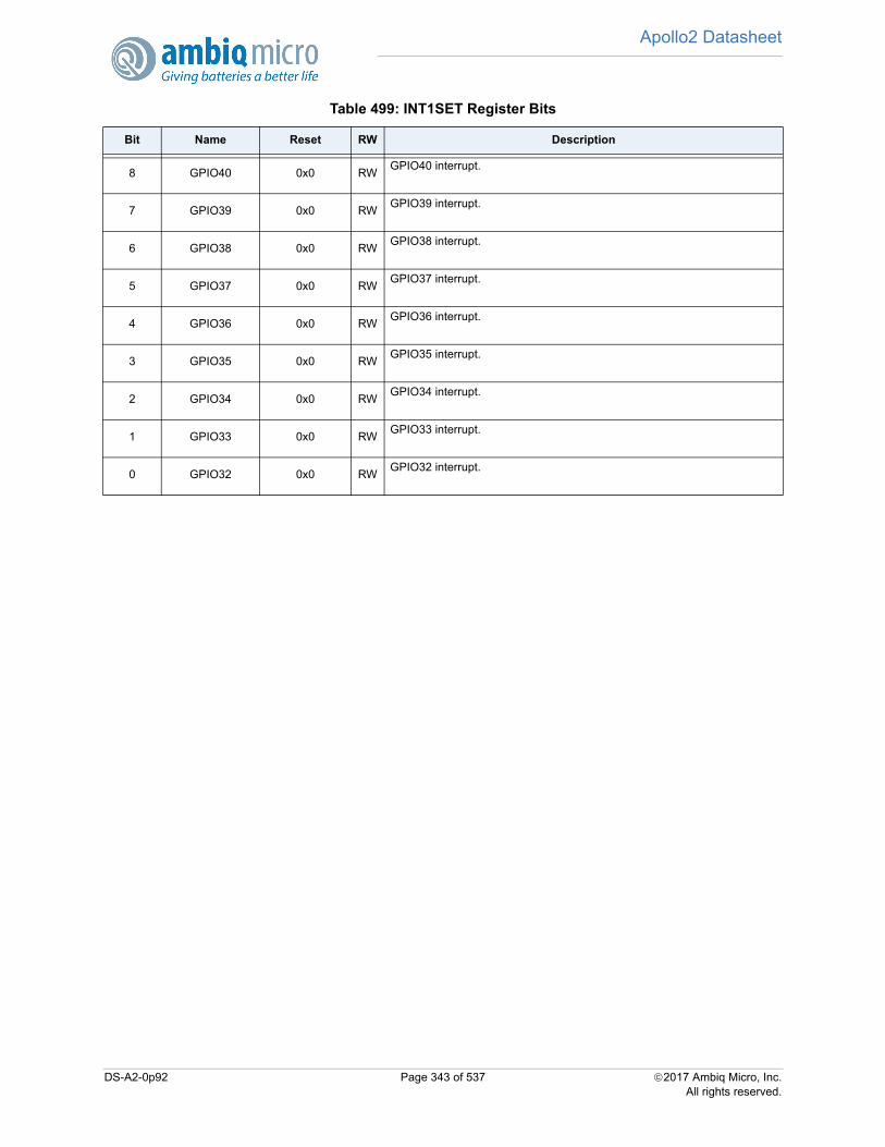
Apollo2 Datasheet
8 GPIO40 0x0 RWGPIO40 interrupt.
7 GPIO39 0x0 RWGPIO39 interrupt.
6 GPIO38 0x0 RWGPIO38 interrupt.
5 GPIO37 0x0 RWGPIO37 interrupt.
4 GPIO36 0x0 RWGPIO36 interrupt.
3 GPIO35 0x0 RWGPIO35 interrupt.
2 GPIO34 0x0 RWGPIO34 interrupt.
1 GPIO33 0x0 RWGPIO33 interrupt.
0 GPIO32 0x0 RWGPIO32 interrupt.
Table 499: INT1SET Register Bits
Bit Name Reset RW Description
DS-A2-0p92 Page 343 of 537 2017 Ambiq Micro, Inc.All rights reserved.
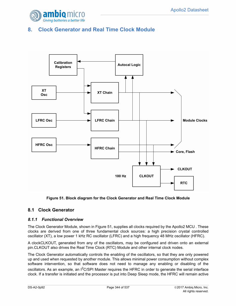
Apollo2 Datasheet
8. Clock Generator and Real Time Clock Module
Figure 51. Block diagram for the Clock Generator and Real Time Clock Module
8.1 Clock Generator
8.1.1 Functional Overview
The Clock Generator Module, shown in Figure 51, supplies all clocks required by the Apollo2 MCU . Theseclocks are derived from one of three fundamental clock sources: a high precision crystal controlledoscillator (XT), a low power 1 kHz RC oscillator (LFRC) and a high frequency 48 MHz oscillator (HFRC).
A clockCLKOUT, generated from any of the oscillators, may be configured and driven onto an externalpin.CLKOUT also drives the Real Time Clock (RTC) Module and other internal clock nodes.
The Clock Generator automatically controls the enabling of the oscillators, so that they are only poweredup and used when requested by another module. This allows minimal power consumption without complexsoftware intervention, so that software does not need to manage any enabling or disabling of the
oscillators. As an example, an I2C/SPI Master requires the HFRC in order to generate the serial interfaceclock. If a transfer is initiated and the processor is put into Deep Sleep mode, the HFRC will remain active
XT Chain
LFRC Chain
HFRC Chain
CLKOUT
CLKOUT
Core, Flash
100 Hz
XTOsc
LFRC Osc
HFRC Osc
Calibration Registers
Module Clocks
Autocal Logic
RTC
DS-A2-0p92 Page 344 of 537 2017 Ambiq Micro, Inc.All rights reserved.
Apollo2 Datasheet
until the I/O transfer is completed. At that point the HFRC will be powered down without requiring anysoftware intervention.
8.1.2 Low Frequency RC Oscillator (LFRC)
The low power LFRC, with a nominal frequency of 1024 Hz, is used when short term frequency accuracy isnot important. It also supplies clocks for some basic state machines and is always enabled. Calibrationlogic is included.
8.1.2.1 LFRC Oscillator Digital Calibration
The LFRC Oscillator includes a patented Distributed Digital Calibration function similar to that of the XTOscillator (Section 8.1.3.2). Because the LFRC Oscillator has a greater fundamental variability, therequired range of calibration is much larger. When the 1024 Hz RC oscillator is selected, the clock at the512 Hz level of the divider chain is modified on a selectable interval using the calibration value CALRC inthe REG_CLKGEN_CALRC Register. Clock pulses are either added or subtracted to ensure accuracy ofthe LFRC. CALRC cycles of the 512 Hz clock are gated (negative calibration) or replaced by 1024 Hzpulses (positive calibration) within every 1024 second calibration period. Each step in CALRC modifies theclock frequency by 1.907 ppm, with a maximum adjustment of +249,954/-249,955 ppm (±25%).
The pulses which are added to or subtracted from the 512 Hz clock are spread evenly over each1024 second period using the Ambiq Micro patented Distributed Calibration algorithm. This ensures that inLFRC mode the maximum cycle-to-cycle jitter in any clock of a frequency 512 Hz or lower caused bycalibration will be no more than one 512 Hz period (~2 ms). This maximum jitter applies to all clocks in theApollo2 MCU which use the LFRC.
Note that since the 512 Hz LFRC clock is calibrated, the 1024 Hz LFRC is an uncalibrated clock. This maybe a useful selection in some cases.
8.1.2.2 LFRC Calibration Process
The LFRC oscillator calibration value is determined by the following process:
1. Set the CALRC field to 0 to insure calibration is not occurring.
2. Select the LFRC oscillator by setting the REG_CLKGEN_OCTRL_OSEL bit to 1.
3. Select the LFRC or a division of it on a CLKOUT pad.
4. Measure the frequency Fmeas at the CLKOUT pad.
5. Compute the adjustment value required in ppm as ((Fnom – Fmeas)*1000000)/Fmeas = PAdj
6. Compute the adjustment value in steps as PAdj/(1000000/2^19) = PAdj/(1.90735) = Adj
7. Compare Adj value with min/max range of -249,955 to 249,954
8. If target Adj is within min and max, set CALRC = Adj
9. Otherwise, the LFRC frequency is too low to be calibrated
8.1.3 High Precision XT Oscillator (XT)
The high accuracy XT Oscillator is tuned to an external 32.768 kHz crystal, and has a nominal frequency of32.768 kHz. It is used when frequency accuracy is critically important. Because a crystal oscillator uses asignificant amount of power, the XT is only enabled when an internal module is using it. Digital calibrationlogic is included.The output of the XT oscillator may be digitally calibrated to ±1 ppm (part per million).
It should be noted that the XT oscillator is also optional if the requirements of the design can tolerate theinternal LFRC/HFRC oscillator specifications. It should also be noted that external capacitors are notrequired to tune an internal divided clock of the crystal input to achieve a precise scaling of 32.768kHz.This is handled within the Apollo2 MCU.
DS-A2-0p92 Page 345 of 537 2017 Ambiq Micro, Inc.All rights reserved.
Apollo2 Datasheet
NOTE: The XTAL is highly sensitive to external leakage on the XI pin. Therefore it is recommended to minimize the components on XI and to use extremely low leakage load capacitors.
8.1.3.1 XT Oscillator Digital Calibration
The XT Oscillator includes a Distributed Digital Calibration function. When the 32 kHz XT oscillator isselected, the clock at the 16 kHz level of the divider chain is modified on a selectable interval using thecalibration value CALXT in the REG_CLKGEN_CALXT Register. Clock pulses are either added orsubtracted to ensure accuracy of the XT. CALXT cycles of the 16 kHz clock are gated (negative calibration)or replaced by 32 kHz pulses (positive calibration) within every 64 second calibration period. Each step inCALXT modifies the clock frequency by 0.9535 ppm, with a maximum adjustment of +975/-976 ppm(±0.1%).
The pulses which are added to or subtracted from the 16 kHz clock are spread evenly over each64 second period using the Ambiq Micro patented Distributed Calibration algorithm. This insures that in XTmode the maximum cycle-to-cycle jitter in any clock of a frequency 16 kHz or lower caused by calibrationwill be no more than one 16 kHz period (~60 us). This maximum jitter applies to all clocks in the Apollo2MCU which use the XT.
Note that since the 16 kHz XT clock is calibrated, the 32 kHz XT is an uncalibrated clock. This may be auseful selection in some cases.
8.1.3.2 XT Calibration Process
The XT Oscillator calibration value is determined by the following process:
1. Set the CALXT register field to 0 to insure calibration is not occurring.
2. Select the XT oscillator by setting the REG_CLKGEN_OCTRL_OSEL bit to 0.
3. Select the XT or a division of it on a CLKOUT pad.
4. Measure the frequency Fmeas at the CLKOUT pad.
5. Compute the adjustment value required in ppm as ((Fnom – Fmeas)*1000000)/Fmeas = PAdj
6. Compute the adjustment value in steps as PAdj/(1000000/219) = PAdj/(0.9535) = Adj
7. Compare Adj value with min/max range of -976 to 975
8. If target Adj is within min and max, set CALXT = Adj
9. Otherwise, the XT frequency is too low to be calibrated.
8.1.3.3 XT Oscillator Failure Detection
If the 32 kHz XT Oscillator generates clocks at less than 8 kHz for a period of more than 32 ms, theApollo2 MCU detects an Oscillator Failure. The OF flag is set when an Oscillator Failure occurs, and isalso set when the Apollo2 MCU initially powers up. If the OFIE bit is set, the OF flag will generate aninterrupt. The current status of the XT Oscillator can be read in the REG_CLKGEN_STATUS_OSCF bit,which will be a 1 if the XT Oscillator is not running at least 8 kHz. Note that OSCF will always be set if theLFRC Oscillator is currently selected by the REG_CLKGEN_OCTRL_OSEL bit.
If the FOS bit is set and the Apollo2 MCU RTC is currently using the XT Oscillator, it will automaticallyswitch to the LFRC Oscillator on an Oscillator Failure. This guarantees that the RTC clock will not stop inany case. If the XT Oscillator experiences a temporary failure and subsequently restarts, the Apollo2 MCUwill switch back to the XT Oscillator. The REG_CLKGEN_STATUS_OMODE bit indicates the currentlyselected oscillator, which may not match the oscillator requested by the REG_CLKGEN_OCTRL_OSEL bitif the XT Oscillator is not running.
DS-A2-0p92 Page 346 of 537 2017 Ambiq Micro, Inc.All rights reserved.
Apollo2 Datasheet
8.1.4 High Frequency RC Oscillator (HFRC)
The high frequency HFRC Oscillator, with a nominal frequency of 48 MHz, is used to supply all highfrequency clocks in the Apollo2 MCU such as the processor clock for the ARM core, memories and manyperipheral modules. Digital calibration is not supported for the HFRC, but its frequency may beautomatically adjusted by the Autoadjustment function which is a combination of analog and digitaloperations.
The HFRC is enabled only when it is required by an internal module. When the ARM core goes into a sleepmode, the HFRC will be disabled unless another module is using it. If the ARM core goes into deep sleepmode, the HFRC will be powered down when it is not needed. When the HFRC is powered up, it will takea few microseconds for it to begin oscillating, and a few more microseconds before the output iscompletely stable. In order to prevent erroneous internal clocks from occurring, the internal clocks aregated until the HFRC is stable.
8.1.5 HFRC Autoadjustment
In some applications it is important that the HFRC frequency be more accurate than the ±2% variationtypically seen, particularly in cases where the temperature may vary widely. A good example of this is incases where the Apollo2 MCU communicates with another device via the UART. The frequency matchingwith the other device in the connection is an important factor in the reliability of the connection. In order tosupport a highly accurate HFRC, a function called Autoadjustment is provided.
It should be noted that Autoadjustment is dependent on an accurate clock source such as the crystal. Themin/max variation of the HFRC frequency with and without adjustment is different. See Section 17.5 onpage 503.
During Autoadjustment, the number of HFRC cycles which occur in one 32.768 kHz XT Oscillator cycle iscompared to a target value. If the count is different from the target, an HFRC tuning value is modified tochange the HFRC frequency. The target count is held in the REG_CLKGEN_HFADJ_HFXTADJ field. If thetarget HFRC frequency is 48 MHz, the optimal HFXTADJ value is 48,000/32.768 or 1464. A different valuewill result in a different nominal HFRC frequency.
Autoadjustment works by periodically enabling the HFRC and the XT, counting the HFRC cycles in a singleXT cycle, subtracting that value from HFXTADJ and adding the resulting difference to the actual HFRCtuning value. The current tuning value may be read back in the REG_CLKGEN_HFTUNERB Register.Autoadjustment is enabled loading the repeat frequency value into the HFADJCK field and then setting theREG_CLKGEN_HFADJ_HFADJEN bit.
Autoadjustment cycles will occur continuously if both the XT and the HFRC are currently requested byother modules. If either oscillator is disabled, Autoadjustment cycles will then occur at intervals determinedby the REG_CLKGEN_HFADJ_HFADJCK field, as shown in the register description. Shorter repeatintervals will result in more accurate HFRC frequencies, especially if the temperature is changing rapidly,but will result in higher power consumption. When an Autoadjustment cycle occurs, if the XT was disabledit is enabled and then a delay occurs to allow the XT to stabilize. This delay is defined by theREG_CLKGEN_HFADJ_HFWARMUP field as defined in the Register document. Once the HFRC isstable, the HFRC is enabled and several Autoadjustments occur, each of which results in a refinement ofthe tuning value. Once those adjustments are complete, the HFRC and XT are powered down unless theyare in use by other functions.
8.1.6 Frequency Measurement
The Autocalibration logic may be used to measure the frequency of an internal clock signal relative to theXT Oscillator frequency. The following steps are required to perform this measurement:
1. Set the REG_CLKGEN_OCTRL_ACAL field to 000.
DS-A2-0p92 Page 347 of 537 2017 Ambiq Micro, Inc.All rights reserved.
Apollo2 Datasheet
2. Clear the ACC interrupt flag.
3. Select the clock to be measured with the CKSEL REG_CLKGEN_CLKOUT_CKSEL field.
4. Set ACAL to 110.
5. Wait for the ACC interrupt flag to be set.
6. Read the REG_CLKGEN_ACALCTR field. This will contain the number of reference clocks which occurred during one cycle of the XT Oscillator
7. Calculate the frequency of the measured clock.
The measured frequency is:
FMEAS = FREF ÷ ACALCTR
where FREF is the frequency of the reference clock and ACALCTR is the value read from ACALCTR whenthe measurement is complete. Note that the longer the measurement period is, the more time themeasurement takes, but the resulting FMEAS will be more accurate.
8.1.7 Generating 100 Hz
The Real Time Clock (RTC) module requires a 100 Hz clock which is provided by the Clock Generator.This clock may come either from the LFRC or the XT Oscillators, as determined by theREG_CLKGEN_OCTRL_OSEL bit. Since 100 Hz is not a simple power of two division of either of theseoscillators, special functions are used to create it.
If the XT Oscillator is selected, 100 Hz is generated by dividing the 2048 Hz division of the XT by 21 for 12iterations and by 20 for 13 iterations out of every 25 clock periods. This produces an effective division of:
(21 * 12 + 20 * 13)/25 = 20.48
producing an exact average frequency of 100 Hz with a maximum jitter of less than 1 ms.
If the LFRC Oscillator is selected, 100 Hz is generated by dividing the 256 Hz division of the LFRC by 2 for11 iterations and by 3 for 14 iterations out of every 25 clock periods. This produces an effective division of:
(2 * 11 + 3 * 14)/25 = 2.56
producing an exact average frequency of 100 Hz with a maximum jitter of less than 8 ms.
8.2 CLKGEN RegistersClock Generator
INSTANCE 0 BASE ADDRESS:0x40004000
DS-A2-0p92 Page 348 of 537 2017 Ambiq Micro, Inc.All rights reserved.

Apollo2 Datasheet
8.2.1 Register Memory Map
Table 500: CLKGEN Register Map
Address(s) Register Name Description
0x40004000 CALXT XT Oscillator Control
0x40004004 CALRC RC Oscillator Control
0x40004008 ACALCTR Autocalibration Counter
0x4000400C OCTRL Oscillator Control
0x40004010 CLKOUT CLKOUT Frequency Select
0x4000401C STATUS Clock Generator Status
0x40004020 HFADJ HFRC Adjustment
0x40004024 HFVAL HFADJ readback
0x40004028 CLOCKEN Clock Enable Status
0x4000402C CLOCKEN2 Clock Enable Status
0x40004030 CLOCKEN3 Clock Enable Status
0x40004034 UARTEN UART Enable
0x40004100 INTEN CLKGEN Interrupt Register: Enable
0x40004104 INTSTAT CLKGEN Interrupt Register: Status
0x40004108 INTCLR CLKGEN Interrupt Register: Clear
0x4000410C INTSET CLKGEN Interrupt Register: Set
DS-A2-0p92 Page 349 of 537 2017 Ambiq Micro, Inc.All rights reserved.
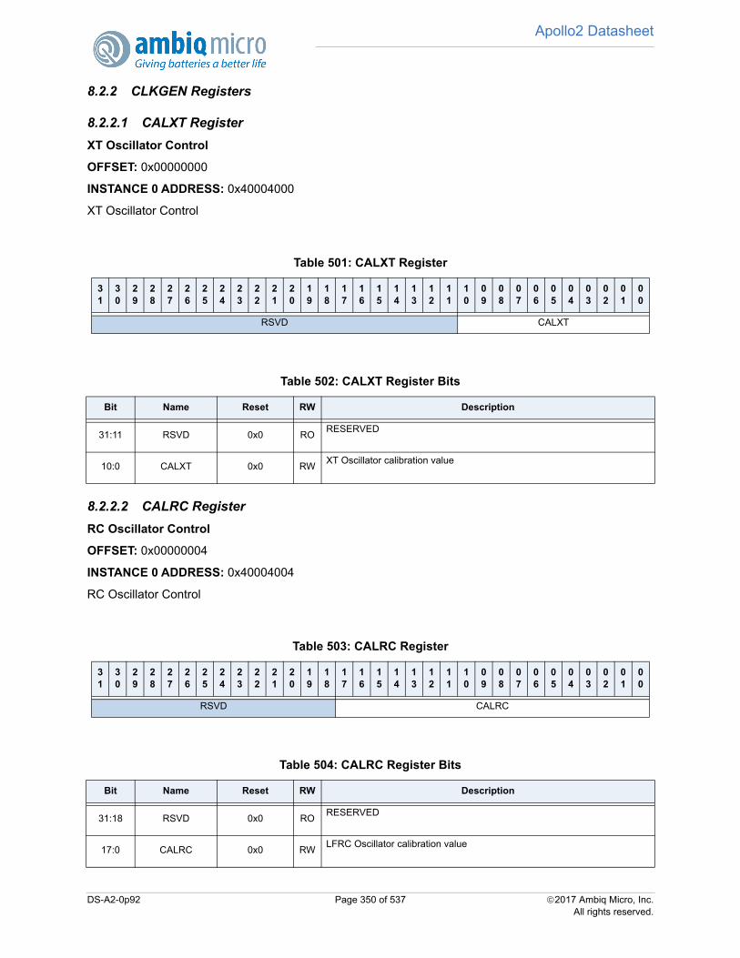
Apollo2 Datasheet
8.2.2 CLKGEN Registers
8.2.2.1 CALXT Register
XT Oscillator Control
OFFSET: 0x00000000
INSTANCE 0 ADDRESS: 0x40004000
XT Oscillator Control
8.2.2.2 CALRC Register
RC Oscillator Control
OFFSET: 0x00000004
INSTANCE 0 ADDRESS: 0x40004004
RC Oscillator Control
Table 501: CALXT Register
31
30
29
28
27
26
25
24
23
22
21
20
19
18
17
16
15
14
13
12
11
10
09
08
07
06
05
04
03
02
01
00
RSVD CALXT
Table 502: CALXT Register Bits
Bit Name Reset RW Description
31:11 RSVD 0x0 RORESERVED
10:0 CALXT 0x0 RWXT Oscillator calibration value
Table 503: CALRC Register
31
30
29
28
27
26
25
24
23
22
21
20
19
18
17
16
15
14
13
12
11
10
09
08
07
06
05
04
03
02
01
00
RSVD CALRC
Table 504: CALRC Register Bits
Bit Name Reset RW Description
31:18 RSVD 0x0 RORESERVED
17:0 CALRC 0x0 RWLFRC Oscillator calibration value
DS-A2-0p92 Page 350 of 537 2017 Ambiq Micro, Inc.All rights reserved.
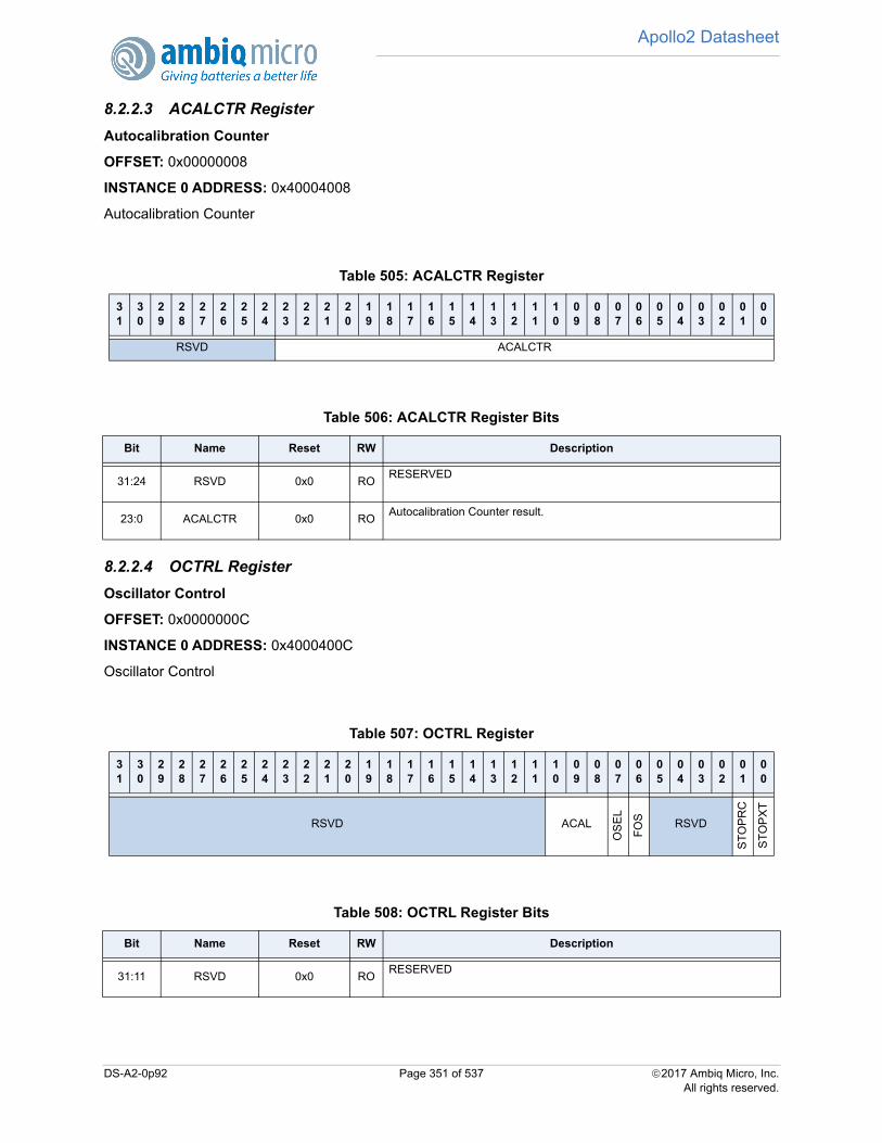
Apollo2 Datasheet
8.2.2.3 ACALCTR Register
Autocalibration Counter
OFFSET: 0x00000008
INSTANCE 0 ADDRESS: 0x40004008
Autocalibration Counter
8.2.2.4 OCTRL Register
Oscillator Control
OFFSET: 0x0000000C
INSTANCE 0 ADDRESS: 0x4000400C
Oscillator Control
Table 505: ACALCTR Register
31
30
29
28
27
26
25
24
23
22
21
20
19
18
17
16
15
14
13
12
11
10
09
08
07
06
05
04
03
02
01
00
RSVD ACALCTR
Table 506: ACALCTR Register Bits
Bit Name Reset RW Description
31:24 RSVD 0x0 RORESERVED
23:0 ACALCTR 0x0 ROAutocalibration Counter result.
Table 507: OCTRL Register
31
30
29
28
27
26
25
24
23
22
21
20
19
18
17
16
15
14
13
12
11
10
09
08
07
06
05
04
03
02
01
00
RSVD ACAL
OS
EL
FO
S RSVD
ST
OP
RC
ST
OP
XT
Table 508: OCTRL Register Bits
Bit Name Reset RW Description
31:11 RSVD 0x0 RORESERVED
DS-A2-0p92 Page 351 of 537 2017 Ambiq Micro, Inc.All rights reserved.
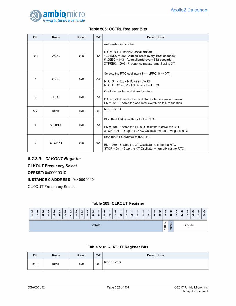
Apollo2 Datasheet
8.2.2.5 CLKOUT Register
CLKOUT Frequency Select
OFFSET: 0x00000010
INSTANCE 0 ADDRESS: 0x40004010
CLKOUT Frequency Select
10:8 ACAL 0x0 RW
Autocalibration control
DIS = 0x0 - Disable Autocalibration1024SEC = 0x2 - Autocalibrate every 1024 seconds512SEC = 0x3 - Autocalibrate every 512 secondsXTFREQ = 0x6 - Frequency measurement using XT
7 OSEL 0x0 RW
Selects the RTC oscillator (1 => LFRC, 0 => XT)
RTC_XT = 0x0 - RTC uses the XTRTC_LFRC = 0x1 - RTC uses the LFRC
6 FOS 0x0 RW
Oscillator switch on failure function
DIS = 0x0 - Disable the oscillator switch on failure functionEN = 0x1 - Enable the oscillator switch on failure function
5:2 RSVD 0x0 RORESERVED
1 STOPRC 0x0 RW
Stop the LFRC Oscillator to the RTC
EN = 0x0 - Enable the LFRC Oscillator to drive the RTCSTOP = 0x1 - Stop the LFRC Oscillator when driving the RTC
0 STOPXT 0x0 RW
Stop the XT Oscillator to the RTC
EN = 0x0 - Enable the XT Oscillator to drive the RTCSTOP = 0x1 - Stop the XT Oscillator when driving the RTC
Table 509: CLKOUT Register
31
30
29
28
27
26
25
24
23
22
21
20
19
18
17
16
15
14
13
12
11
10
09
08
07
06
05
04
03
02
01
00
RSVD
CK
EN
RS
VD
CKSEL
Table 510: CLKOUT Register Bits
Bit Name Reset RW Description
31:8 RSVD 0x0 RORESERVED
Table 508: OCTRL Register Bits
Bit Name Reset RW Description
DS-A2-0p92 Page 352 of 537 2017 Ambiq Micro, Inc.All rights reserved.
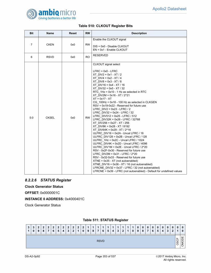
Apollo2 Datasheet
8.2.2.6 STATUS Register
Clock Generator Status
OFFSET: 0x0000001C
INSTANCE 0 ADDRESS: 0x4000401C
Clock Generator Status
7 CKEN 0x0 RW
Enable the CLKOUT signal
DIS = 0x0 - Disable CLKOUTEN = 0x1 - Enable CLKOUT
6 RSVD 0x0 RORESERVED
5:0 CKSEL 0x0 RW
CLKOUT signal select
LFRC = 0x0 - LFRCXT_DIV2 = 0x1 - XT / 2XT_DIV4 = 0x2 - XT / 4XT_DIV8 = 0x3 - XT / 8XT_DIV16 = 0x4 - XT / 16XT_DIV32 = 0x5 - XT / 32RTC_1Hz = 0x10 - 1 Hz as selected in RTCXT_DIV2M = 0x16 - XT / 2^21XT = 0x17 - XTCG_100Hz = 0x18 - 100 Hz as selected in CLKGENRSV = 0x19-0x22 - Reserved for future useLFRC_DIV2 = 0x23 - LFRC / 2LFRC_DIV32 = 0x24 - LFRC / 32LFRC_DIV512 = 0x25 - LFRC / 512LFRC_DIV32K = 0x26 - LFRC / 32768XT_DIV256 = 0x27 - XT / 256XT_DIV8K = 0x28 - XT / 8192XT_DIV64K = 0x29 - XT / 2^16ULFRC_DIV16 = 0x2A - Uncal LFRC / 16ULFRC_DIV128 = 0x2B - Uncal LFRC / 128ULFRC_1Hz = 0x2C - Uncal LFRC / 1024ULFRC_DIV4K = 0x2D - Uncal LFRC / 4096ULFRC_DIV1M = 0x2E - Uncal LFRC / 2^20RSV - 0x2F-0x30 - Reserved for future useLFRC_DIV2M = 0x31 - LFRC / 2^20RSV - 0x32-0x33 - Reserved for future useXTNE = 0x35 - XT (not autoenabled)XTNE_DIV16 = 0x36 - XT / 16 (not autoenabled)LFRCNE_DIV32 = 0x37 - LFRC / 32 (not autoenabled)LFRCNE = 0x39 - LFRC (not autoenabled) - Default for undefined values
Table 511: STATUS Register
31
30
29
28
27
26
25
24
23
22
21
20
19
18
17
16
15
14
13
12
11
10
09
08
07
06
05
04
03
02
01
00
RSVD
OS
CF
OM
OD
E
Table 510: CLKOUT Register Bits
Bit Name Reset RW Description
DS-A2-0p92 Page 353 of 537 2017 Ambiq Micro, Inc.All rights reserved.
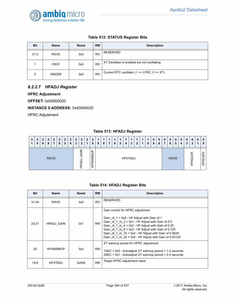
Apollo2 Datasheet
8.2.2.7 HFADJ Register
HFRC Adjustment
OFFSET: 0x00000020
INSTANCE 0 ADDRESS: 0x40004020
HFRC Adjustment
Table 512: STATUS Register Bits
Bit Name Reset RW Description
31:2 RSVD 0x0 RORESERVED
1 OSCF 0x0 ROXT Oscillator is enabled but not oscillating
0 OMODE 0x0 ROCurrent RTC oscillator (1 => LFRC, 0 => XT)
Table 513: HFADJ Register
31
30
29
28
27
26
25
24
23
22
21
20
19
18
17
16
15
14
13
12
11
10
09
08
07
06
05
04
03
02
01
00
RSVD
HFA
DJ_
GA
IN
HF
WA
RM
UP
HFXTADJ RSVD
HFA
DJC
K
HFA
DJE
N
Table 514: HFADJ Register Bits
Bit Name Reset RW Description
31:24 RSVD 0x0 RORESERVED
23:21 HFADJ_GAIN 0x1 RW
Gain control for HFRC adjustment
Gain_of_1 = 0x0 - HF Adjust with Gain of 1Gain_of_1_in_2 = 0x1 - HF Adjust with Gain of 0.5Gain_of_1_in_4 = 0x2 - HF Adjust with Gain of 0.25Gain_of_1_in_8 = 0x3 - HF Adjust with Gain of 0.125Gain_of_1_in_16 = 0x4 - HF Adjust with Gain of 0.0625Gain_of_1_in_32 = 0x5 - HF Adjust with Gain of 0.03125
20 HFWARMUP 0x0 RW
XT warmup period for HFRC adjustment
1SEC = 0x0 - Autoadjust XT warmup period = 1-2 seconds2SEC = 0x1 - Autoadjust XT warmup period = 2-4 seconds
19:8 HFXTADJ 0x5b8 RWTarget HFRC adjustment value.
DS-A2-0p92 Page 354 of 537 2017 Ambiq Micro, Inc.All rights reserved.
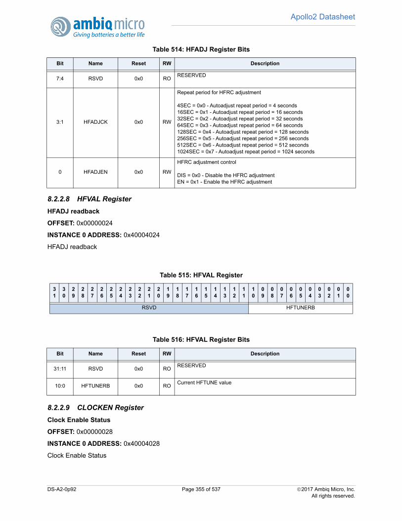
Apollo2 Datasheet
8.2.2.8 HFVAL Register
HFADJ readback
OFFSET: 0x00000024
INSTANCE 0 ADDRESS: 0x40004024
HFADJ readback
8.2.2.9 CLOCKEN Register
Clock Enable Status
OFFSET: 0x00000028
INSTANCE 0 ADDRESS: 0x40004028
Clock Enable Status
7:4 RSVD 0x0 RORESERVED
3:1 HFADJCK 0x0 RW
Repeat period for HFRC adjustment
4SEC = 0x0 - Autoadjust repeat period = 4 seconds16SEC = 0x1 - Autoadjust repeat period = 16 seconds32SEC = 0x2 - Autoadjust repeat period = 32 seconds64SEC = 0x3 - Autoadjust repeat period = 64 seconds128SEC = 0x4 - Autoadjust repeat period = 128 seconds256SEC = 0x5 - Autoadjust repeat period = 256 seconds512SEC = 0x6 - Autoadjust repeat period = 512 seconds1024SEC = 0x7 - Autoadjust repeat period = 1024 seconds
0 HFADJEN 0x0 RW
HFRC adjustment control
DIS = 0x0 - Disable the HFRC adjustmentEN = 0x1 - Enable the HFRC adjustment
Table 515: HFVAL Register
31
30
29
28
27
26
25
24
23
22
21
20
19
18
17
16
15
14
13
12
11
10
09
08
07
06
05
04
03
02
01
00
RSVD HFTUNERB
Table 516: HFVAL Register Bits
Bit Name Reset RW Description
31:11 RSVD 0x0 RORESERVED
10:0 HFTUNERB 0x0 ROCurrent HFTUNE value
Table 514: HFADJ Register Bits
Bit Name Reset RW Description
DS-A2-0p92 Page 355 of 537 2017 Ambiq Micro, Inc.All rights reserved.
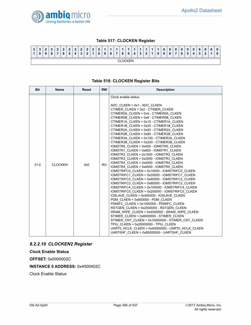
Apollo2 Datasheet
8.2.2.10 CLOCKEN2 Register
Clock Enable Status
OFFSET: 0x0000002C
INSTANCE 0 ADDRESS: 0x4000402C
Clock Enable Status
Table 517: CLOCKEN Register
31
30
29
28
27
26
25
24
23
22
21
20
19
18
17
16
15
14
13
12
11
10
09
08
07
06
05
04
03
02
01
00
CLOCKEN
Table 518: CLOCKEN Register Bits
Bit Name Reset RW Description
31:0 CLOCKEN 0x0 RO
Clock enable status
ADC_CLKEN = 0x1 - ADC_CLKENCTIMER_CLKEN = 0x2 - CTIMER_CLKENCTIMER0A_CLKEN = 0x4 - CTIMER0A_CLKENCTIMER0B_CLKEN = 0x8 - CTIMER0B_CLKENCTIMER1A_CLKEN = 0x10 - CTIMER1A_CLKENCTIMER1B_CLKEN = 0x20 - CTIMER1B_CLKENCTIMER2A_CLKEN = 0x40 - CTIMER2A_CLKENCTIMER2B_CLKEN = 0x80 - CTIMER2B_CLKENCTIMER3A_CLKEN = 0x100 - CTIMER3A_CLKENCTIMER3B_CLKEN = 0x200 - CTIMER3B_CLKENIOMSTR0_CLKEN = 0x400 - IOMSTR0_CLKENIOMSTR1_CLKEN = 0x800 - IOMSTR1_CLKENIOMSTR2_CLKEN = 0x1000 - IOMSTR2_CLKENIOMSTR3_CLKEN = 0x2000 - IOMSTR3_CLKENIOMSTR4_CLKEN = 0x4000 - IOMSTR4_CLKENIOMSTR5_CLKEN = 0x8000 - IOMSTR5_CLKENIOMSTRIFC0_CLKEN = 0x10000 - IOMSTRIFC0_CLKENIOMSTRIFC1_CLKEN = 0x20000 - IOMSTRIFC1_CLKENIOMSTRIFC2_CLKEN = 0x40000 - IOMSTRIFC2_CLKENIOMSTRIFC3_CLKEN = 0x80000 - IOMSTRIFC3_CLKENIOMSTRIFC4_CLKEN = 0x100000 - IOMSTRIFC4_CLKENIOMSTRIFC5_CLKEN = 0x200000 - IOMSTRIFC5_CLKENIOSLAVE_CLKEN = 0x400000 - IOSLAVE_CLKENPDM_CLKEN = 0x800000 - PDM_CLKENPDMIFC_CLKEN = 0x1000000 - PDMIFC_CLKENRSTGEN_CLKEN = 0x2000000 - RSTGEN_CLKENSRAM_WIPE_CLKEN = 0x4000000 - SRAM_WIPE_CLKENSTIMER_CLKEN = 0x8000000 - STIMER_CLKENSTIMER_CNT_CLKEN = 0x10000000 - STIMER_CNT_CLKENTPIU_CLKEN = 0x20000000 - TPIU_CLKENUART0_HCLK_CLKEN = 0x40000000 - UART0_HCLK_CLKENUART0HF_CLKEN = 0x80000000 - UART0HF_CLKEN
DS-A2-0p92 Page 356 of 537 2017 Ambiq Micro, Inc.All rights reserved.

Apollo2 Datasheet
8.2.2.11 CLOCKEN3 Register
Clock Enable Status
OFFSET: 0x00000030
INSTANCE 0 ADDRESS: 0x40004030
Clock Enable Status
Table 519: CLOCKEN2 Register
31
30
29
28
27
26
25
24
23
22
21
20
19
18
17
16
15
14
13
12
11
10
09
08
07
06
05
04
03
02
01
00
CLOCKEN2
Table 520: CLOCKEN2 Register Bits
Bit Name Reset RW Description
31:0 CLOCKEN2 0x0 RO
Clock enable status 2
UART1_HCLK_CLKEN = 0x1 - UART1_HCLK_CLKENUART1HF_CLKEN = 0x2 - UART1HF_CLKENWDT_CLKEN = 0x4 - WDT_CLKENXT_32KHz_EN = 0x40000000 - XT_32KHz_ENFRCHFRC = 0x80000000 - Force HFRC On Status
Table 521: CLOCKEN3 Register
31
30
29
28
27
26
25
24
23
22
21
20
19
18
17
16
15
14
13
12
11
10
09
08
07
06
05
04
03
02
01
00
CLOCKEN3
Table 522: CLOCKEN3 Register Bits
Bit Name Reset RW Description
31:0 CLOCKEN3 0x0 RO
Clock enable status 3
periph_all_xtal_en = 0x1000000 - At least 1 peripherial is requesting forXTAL Clockperiph_all_hfrc_en = 0x2000000 - At least 1 peripherial is requesting forHFRC ClockHFADJEN = 0x4000000 - HFRC Adjust Enable StatusHFRC_en_out = 0x8000000 - HFRC is enabled during adjustment statusRTC_SOURCE = 0x10000000 - Selects the RTC oscillator (0 => LFRC, 1=> XT)XTAL_EN = 0x20000000 - XT is enabled StatusHFRC_EN = 0x40000000 - HFRC is enabled StatusFLASHCLK_EN = 0x80000000 - Flash Clock is enabled Status
DS-A2-0p92 Page 357 of 537 2017 Ambiq Micro, Inc.All rights reserved.
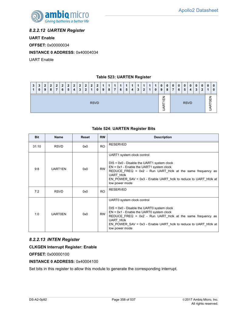
Apollo2 Datasheet
8.2.2.12 UARTEN Register
UART Enable
OFFSET: 0x00000034
INSTANCE 0 ADDRESS: 0x40004034
UART Enable
8.2.2.13 INTEN Register
CLKGEN Interrupt Register: Enable
OFFSET: 0x00000100
INSTANCE 0 ADDRESS: 0x40004100
Set bits in this register to allow this module to generate the corresponding interrupt.
Table 523: UARTEN Register
31
30
29
28
27
26
25
24
23
22
21
20
19
18
17
16
15
14
13
12
11
10
09
08
07
06
05
04
03
02
01
00
RSVD
UA
RT
1EN
RSVD
UA
RT
0EN
Table 524: UARTEN Register Bits
Bit Name Reset RW Description
31:10 RSVD 0x0 RORESERVED
9:8 UART1EN 0x0 RW
UART1 system clock control
DIS = 0x0 - Disable the UART1 system clockEN = 0x1 - Enable the UART1 system clockREDUCE_FREQ = 0x2 - Run UART_Hclk at the same frequency asUART_hfclkEN_POWER_SAV = 0x3 - Enable UART_hclk to reduce to UART_hfclk atlow power mode
7:2 RSVD 0x0 RORESERVED
1:0 UART0EN 0x0 RW
UART0 system clock control
DIS = 0x0 - Disable the UART0 system clockEN = 0x1 - Enable the UART0 system clockREDUCE_FREQ = 0x2 - Run UART_Hclk at the same frequency asUART_hfclkEN_POWER_SAV = 0x3 - Enable UART_hclk to reduce to UART_hfclk atlow power mode
DS-A2-0p92 Page 358 of 537 2017 Ambiq Micro, Inc.All rights reserved.
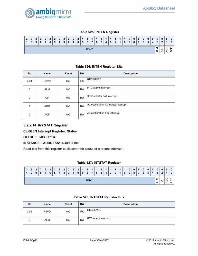
Apollo2 Datasheet
8.2.2.14 INTSTAT Register
CLKGEN Interrupt Register: Status
OFFSET: 0x00000104
INSTANCE 0 ADDRESS: 0x40004104
Read bits from this register to discover the cause of a recent interrupt.
Table 525: INTEN Register
31
30
29
28
27
26
25
24
23
22
21
20
19
18
17
16
15
14
13
12
11
10
09
08
07
06
05
04
03
02
01
00
RSVD
ALM OF
AC
C
AC
F
Table 526: INTEN Register Bits
Bit Name Reset RW Description
31:4 RSVD 0x0 RORESERVED
3 ALM 0x0 RWRTC Alarm interrupt
2 OF 0x0 RWXT Oscillator Fail interrupt
1 ACC 0x0 RWAutocalibration Complete interrupt
0 ACF 0x0 RWAutocalibration Fail interrupt
Table 527: INTSTAT Register
31
30
29
28
27
26
25
24
23
22
21
20
19
18
17
16
15
14
13
12
11
10
09
08
07
06
05
04
03
02
01
00
RSVD
AL
M
OF
AC
C
AC
F
Table 528: INTSTAT Register Bits
Bit Name Reset RW Description
31:4 RSVD 0x0 RORESERVED
3 ALM 0x0 RWRTC Alarm interrupt
DS-A2-0p92 Page 359 of 537 2017 Ambiq Micro, Inc.All rights reserved.
Apollo2 Datasheet
8.2.2.15 INTCLR Register
CLKGEN Interrupt Register: Clear
OFFSET: 0x00000108
INSTANCE 0 ADDRESS: 0x40004108
Write a 1 to a bit in this register to clear the interrupt status associated with that bit.
8.2.2.16 INTSET Register
CLKGEN Interrupt Register: Set
OFFSET: 0x0000010C
INSTANCE 0 ADDRESS: 0x4000410C
Write a 1 to a bit in this register to instantly generate an interrupt from this module. (Generally used fortesting purposes).
2 OF 0x0 RWXT Oscillator Fail interrupt
1 ACC 0x0 RWAutocalibration Complete interrupt
0 ACF 0x0 RWAutocalibration Fail interrupt
Table 529: INTCLR Register
31
30
29
28
27
26
25
24
23
22
21
20
19
18
17
16
15
14
13
12
11
10
09
08
07
06
05
04
03
02
01
00
RSVD
ALM OF
AC
C
AC
F
Table 530: INTCLR Register Bits
Bit Name Reset RW Description
31:4 RSVD 0x0 RORESERVED
3 ALM 0x0 RWRTC Alarm interrupt
2 OF 0x0 RWXT Oscillator Fail interrupt
1 ACC 0x0 RWAutocalibration Complete interrupt
0 ACF 0x0 RWAutocalibration Fail interrupt
Table 528: INTSTAT Register Bits
Bit Name Reset RW Description
DS-A2-0p92 Page 360 of 537 2017 Ambiq Micro, Inc.All rights reserved.
Apollo2 Datasheet
Table 531: INTSET Register
31
30
29
28
27
26
25
24
23
22
21
20
19
18
17
16
15
14
13
12
11
10
09
08
07
06
05
04
03
02
01
00
RSVD
ALM OF
AC
C
AC
F
Table 532: INTSET Register Bits
Bit Name Reset RW Description
31:4 RSVD 0x0 RORESERVED
3 ALM 0x0 RWRTC Alarm interrupt
2 OF 0x0 RWXT Oscillator Fail interrupt
1 ACC 0x0 RWAutocalibration Complete interrupt
0 ACF 0x0 RWAutocalibration Fail interrupt
DS-A2-0p92 Page 361 of 537 2017 Ambiq Micro, Inc.All rights reserved.
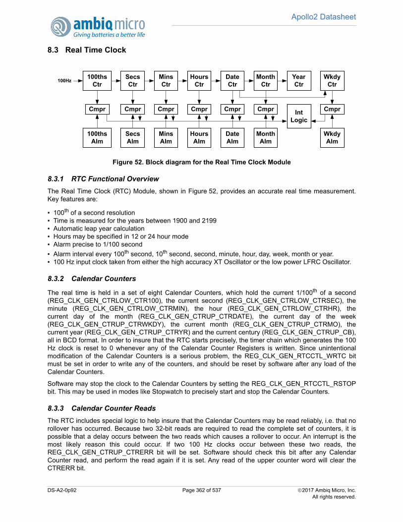
Apollo2 Datasheet
8.3 Real Time Clock
Figure 52. Block diagram for the Real Time Clock Module
8.3.1 RTC Functional Overview
The Real Time Clock (RTC) Module, shown in Figure 52, provides an accurate real time measurement.Key features are:
100th of a second resolution Time is measured for the years between 1900 and 2199 Automatic leap year calculation Hours may be specified in 12 or 24 hour mode Alarm precise to 1/100 second
Alarm interval every 100th second, 10th second, second, minute, hour, day, week, month or year. 100 Hz input clock taken from either the high accuracy XT Oscillator or the low power LFRC Oscillator.
8.3.2 Calendar Counters
The real time is held in a set of eight Calendar Counters, which hold the current 1/100th of a second(REG_CLK_GEN_CTRLOW_CTR100), the current second (REG_CLK_GEN_CTRLOW_CTRSEC), theminute (REG_CLK_GEN_CTRLOW_CTRMIN), the hour (REG_CLK_GEN_CTRLOW_CTRHR), thecurrent day of the month (REG_CLK_GEN_CTRUP_CTRDATE), the current day of the week(REG_CLK_GEN_CTRUP_CTRWKDY), the current month (REG_CLK_GEN_CTRUP_CTRMO), thecurrent year (REG_CLK_GEN_CTRUP_CTRYR) and the current century (REG_CLK_GEN_CTRUP_CB),all in BCD format. In order to insure that the RTC starts precisely, the timer chain which generates the 100Hz clock is reset to 0 whenever any of the Calendar Counter Registers is written. Since unintentionalmodification of the Calendar Counters is a serious problem, the REG_CLK_GEN_RTCCTL_WRTC bitmust be set in order to write any of the counters, and should be reset by software after any load of theCalendar Counters.
Software may stop the clock to the Calendar Counters by setting the REG_CLK_GEN_RTCCTL_RSTOPbit. This may be used in modes like Stopwatch to precisely start and stop the Calendar Counters.
8.3.3 Calendar Counter Reads
The RTC includes special logic to help insure that the Calendar Counters may be read reliably, i.e. that norollover has occurred. Because two 32-bit reads are required to read the complete set of counters, it ispossible that a delay occurs between the two reads which causes a rollover to occur. An interrupt is themost likely reason this could occur. If two 100 Hz clocks occur between these two reads, theREG_CLK_GEN_CTRUP_CTRERR bit will be set. Software should check this bit after any CalendarCounter read, and perform the read again if it is set. Any read of the upper counter word will clear theCTRERR bit.
100ths Ctr100Hz
Secs Ctr
Mins Ctr
Hours Ctr
Date Ctr
Month Ctr
Year Ctr
Wkdy Ctr
100ths Alm
Secs Alm
Mins Alm
Hours Alm
Date Alm
Month Alm
Wkdy Alm
Cmpr Cmpr Cmpr Cmpr Cmpr Cmpr CmprInt Logic
DS-A2-0p92 Page 362 of 537 2017 Ambiq Micro, Inc.All rights reserved.

Apollo2 Datasheet
8.3.4 Alarms
There are seven Alarm Registers which may be used to generate an Alarm interrupt at a specific time.
These registers correspond to the 100th of a second (REG_CLK_GEN_ALMLOW_ALM100), second(REG_CLK_GEN_ALMLOW_ALMSEC), minute (REG_CLK_GEN_ALMLOW_ALMMIN), hour(REG_CLK_GEN_ALMLOW_ALMHR), day of the month (REG_CLK_GEN_ALMUP_ALMDATE), day ofthe week (REG_CLK_GEN_ALMUP_ALMWKDY) and month (REG_CLK_GEN_ALMUP_ALMMO)Calendar Counters. The comparison is controlled by the REG_CLK_GEN_RTCCTL_RPT field and theREG_CLK_GEN_ALMLOW_ALM100 Register as shown in 12/24 Hour Mode. In the ALM100 Register, nindicates any digit 0-9. When all selected Counters match their corresponding Alarm Register, the ALMinterrupt flag is set (see the Clock Generator section for the ALM interrupt control).
All alarm interrupts are asserted on the next 100 Hz clock cycle after the counters match the alarm register,except for 100ths of a second. To get an interrupt that occurs precisely at a certain time, the comparisonvalue in the corresponding alarm register should be set 10 ms (one 100 Hz count) earlier than the desiredinterrupt time.
For the 100ths of a second interrupt, the first 100 Hz clock sets the comparison with the alarm register andthe next clock asserts the interrupt. Therefore, the first 100ths interrupt will be asserted after 20 ms, not10 ms. This occurs each and every time the 100ths of a second counter with interrupts is enabled if theRTC is stopped. If the RTC is already running when configured, then the first interrupt will occur between10 and 20 ms after configuration.
8.3.5 12/24 Hour Mode
If the REG_CLK_GEN_RTCCTL_HR1224 bit is 0, the RTC is in 24-hour mode, and the Hours and HoursAlarm Registers hold a 6-bit BCD value which is the 24-hour time (values 0 to 23). If the HR1224 bit is 1,the RTC is in 12-hour mode, and the Hours and Hours Alarm Registers hold a 5-bit BCD value which is the12-hour time (values 1 to 12) , and bit 5 is the AP bit which is 0 for an AM time and 1 for a PM time. If theHR1224 bit is modified the Hours and Hours Alarm fields must be updated.
8.3.6 Century Control and Leap Year Management
The REG_CLK_GEN_CTRUP_CB bit indicates the current century. A value of 0 indicates the 20th century,
and a value of 1 indicates the 19th or 21st century. The CB value will toggle when the Years counter rollsover from 99 to 0 if the REG_CLK_GEN_CTRUP_CEB bit is set, and will remain constant if CEB is clear.
Table 533: Alarm RPT Function
RPT Value ALM100 Interval Comparison
000 0xnn Disabled None
000 0xnn Every year 100th, second, minute, hour, day, month
000 0xnn Every month 100th, second, minute, hour, day
001 0xnn Every week 100th, second, minute, hour, weekday
010 0xnn Every day 100th, second, minute, hour
011 0xnn Every hour 100th, second, minute
100 0xnn Every minute 100th, second
101 0xnn Every second 100th
110 0xFn Every 10th Upper nibble of 100th
111 0xFF Every 100th None
DS-A2-0p92 Page 363 of 537 2017 Ambiq Micro, Inc.All rights reserved.

Apollo2 Datasheet
The century value is used to control the Leap Year functions, which create the correct insertion of February29 in years which are divisible by 4 and not divisible by 100, and also the year 2000.
8.3.7 Weekday Function
The Weekday Counter is simply a 3-bit counter which counts up to 6 and then resets to 0. It is theresponsibility of software to assign particular days of the week to each counter value.
8.4 RTC Registers
Real Time Clock
INSTANCE 0 BASE ADDRESS:0x40004000
8.4.1 Register Memory Map
Table 535: INTSET Register Bits
Bit Name Reset RW Description
31:4 RSVD 0x0 RORESERVED
3 ALM 0x0 RWRTC Alarm interrupt
2 OF 0x0 RWXT Oscillator Fail interrupt
1 ACC 0x0 RWAutocalibration Complete interrupt
0 ACF 0x0 RWAutocalibration Fail interrupt
Table 536: RTC Register Map
Address(s) Register Name Description
0x40004040 CTRLOW RTC Counters Lower
0x40004044 CTRUP RTC Counters Upper
0x40004048 ALMLOW RTC Alarms Lower
0x4000404C ALMUP RTC Alarms Upper
0x40004050 RTCCTL RTC Control Register
0x40004100 INTEN RTC Interrupt Register: Enable
0x40004104 INTSTAT RTC Interrupt Register: Status
0x40004108 INTCLR RTC Interrupt Register: Clear
0x4000410C INTSET RTC Interrupt Register: Set
DS-A2-0p92 Page 364 of 537 2017 Ambiq Micro, Inc.All rights reserved.

Apollo2 Datasheet
8.4.2 RTC Registers
8.4.2.1 CTRLOW Register
RTC Counters Lower
OFFSET: 0x00000040
INSTANCE 0 ADDRESS: 0x40004040
RTC Counters Lower
8.4.2.2 CTRUP Register
RTC Counters Upper
OFFSET: 0x00000044
INSTANCE 0 ADDRESS: 0x40004044
RTC Counters Upper
Table 537: CTRLOW Register
31
30
29
28
27
26
25
24
23
22
21
20
19
18
17
16
15
14
13
12
11
10
09
08
07
06
05
04
03
02
01
00
RS
VD
CTRHR
RS
VD
CTRMIN
RS
VD
CTRSEC CTR100
Table 538: CTRLOW Register Bits
Bit Name Reset RW Description
31:30 RSVD 0x0 RORESERVED
29:24 CTRHR 0x1 RWHours Counter
23 RSVD 0x0 RORESERVED
22:16 CTRMIN 0x0 RWMinutes Counter
15 RSVD 0x0 RORESERVED
14:8 CTRSEC 0x0 RWSeconds Counter
7:0 CTR100 0x0 RW100ths of a second Counter
DS-A2-0p92 Page 365 of 537 2017 Ambiq Micro, Inc.All rights reserved.
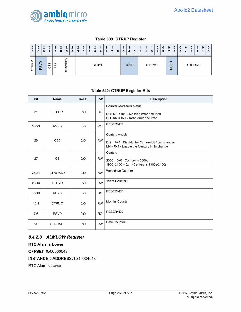
Apollo2 Datasheet
8.4.2.3 ALMLOW Register
RTC Alarms Lower
OFFSET: 0x00000048
INSTANCE 0 ADDRESS: 0x40004048
RTC Alarms Lower
Table 539: CTRUP Register
31
30
29
28
27
26
25
24
23
22
21
20
19
18
17
16
15
14
13
12
11
10
09
08
07
06
05
04
03
02
01
00
CT
ER
R
RS
VD
CE
B
CB
CT
RW
KD
YCTRYR RSVD CTRMO
RS
VD
CTRDATE
Table 540: CTRUP Register Bits
Bit Name Reset RW Description
31 CTERR 0x0 RO
Counter read error status
NOERR = 0x0 - No read error occurredRDERR = 0x1 - Read error occurred
30:29 RSVD 0x0 RORESERVED
28 CEB 0x0 RW
Century enable
DIS = 0x0 - Disable the Century bit from changingEN = 0x1 - Enable the Century bit to change
27 CB 0x0 RW
Century
2000 = 0x0 - Century is 2000s1900_2100 = 0x1 - Century is 1900s/2100s
26:24 CTRWKDY 0x0 RWWeekdays Counter
23:16 CTRYR 0x0 RWYears Counter
15:13 RSVD 0x0 RORESERVED
12:8 CTRMO 0x0 RWMonths Counter
7:6 RSVD 0x0 RORESERVED
5:0 CTRDATE 0x0 RWDate Counter
DS-A2-0p92 Page 366 of 537 2017 Ambiq Micro, Inc.All rights reserved.

Apollo2 Datasheet
8.4.2.4 ALMUP Register
RTC Alarms Upper
OFFSET: 0x0000004C
INSTANCE 0 ADDRESS: 0x4000404C
RTC Alarms Upper
Table 541: ALMLOW Register
31
30
29
28
27
26
25
24
23
22
21
20
19
18
17
16
15
14
13
12
11
10
09
08
07
06
05
04
03
02
01
00
RS
VD
ALMHR
RS
VD
ALMMIN
RS
VD
ALMSEC ALM100
Table 542: ALMLOW Register Bits
Bit Name Reset RW Description
31:30 RSVD 0x0 RORESERVED
29:24 ALMHR 0x0 RWHours Alarm
23 RSVD 0x0 RORESERVED
22:16 ALMMIN 0x0 RWMinutes Alarm
15 RSVD 0x0 RORESERVED
14:8 ALMSEC 0x0 RWSeconds Alarm
7:0 ALM100 0x0 RW100ths of a second Alarm
Table 543: ALMUP Register
31
30
29
28
27
26
25
24
23
22
21
20
19
18
17
16
15
14
13
12
11
10
09
08
07
06
05
04
03
02
01
00
RSVD
ALM
WK
DY
RSVD ALMMO
RS
VD
ALMDATE
DS-A2-0p92 Page 367 of 537 2017 Ambiq Micro, Inc.All rights reserved.
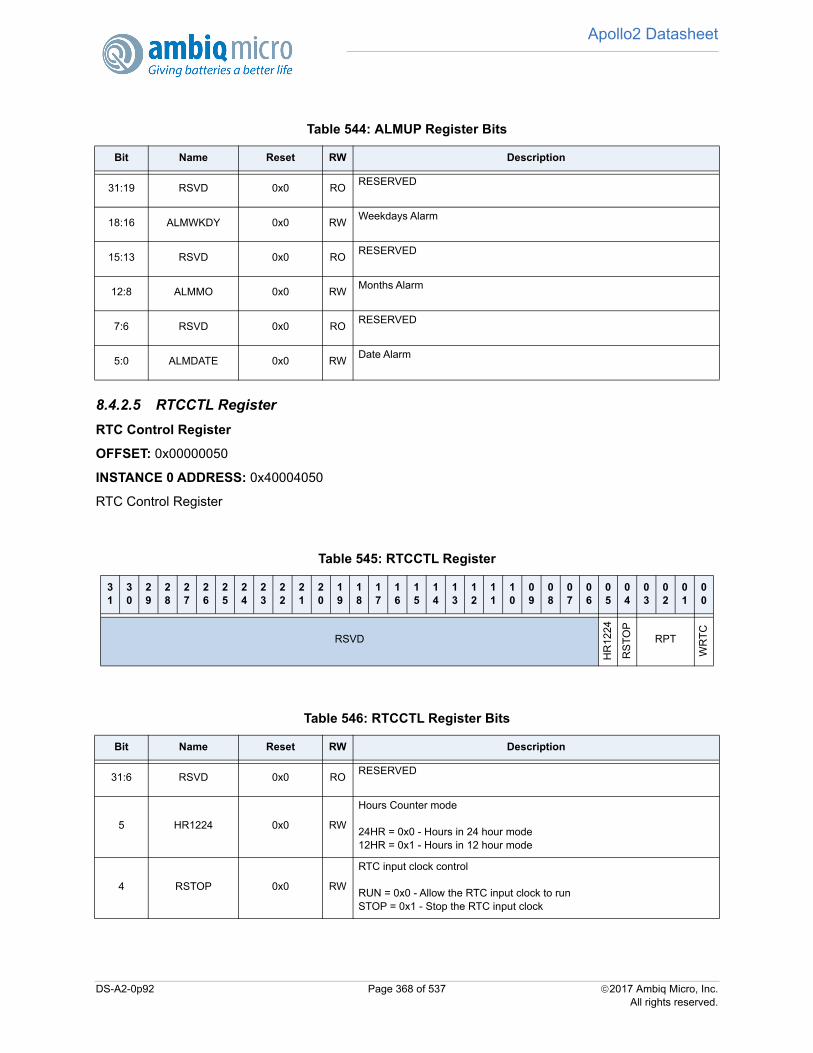
Apollo2 Datasheet
8.4.2.5 RTCCTL Register
RTC Control Register
OFFSET: 0x00000050
INSTANCE 0 ADDRESS: 0x40004050
RTC Control Register
Table 544: ALMUP Register Bits
Bit Name Reset RW Description
31:19 RSVD 0x0 RORESERVED
18:16 ALMWKDY 0x0 RWWeekdays Alarm
15:13 RSVD 0x0 RORESERVED
12:8 ALMMO 0x0 RWMonths Alarm
7:6 RSVD 0x0 RORESERVED
5:0 ALMDATE 0x0 RWDate Alarm
Table 545: RTCCTL Register
31
30
29
28
27
26
25
24
23
22
21
20
19
18
17
16
15
14
13
12
11
10
09
08
07
06
05
04
03
02
01
00
RSVD
HR
1224
RS
TO
PRPT
WR
TC
Table 546: RTCCTL Register Bits
Bit Name Reset RW Description
31:6 RSVD 0x0 RORESERVED
5 HR1224 0x0 RW
Hours Counter mode
24HR = 0x0 - Hours in 24 hour mode12HR = 0x1 - Hours in 12 hour mode
4 RSTOP 0x0 RW
RTC input clock control
RUN = 0x0 - Allow the RTC input clock to runSTOP = 0x1 - Stop the RTC input clock
DS-A2-0p92 Page 368 of 537 2017 Ambiq Micro, Inc.All rights reserved.

Apollo2 Datasheet
8.4.2.6 INTEN Register
RTC Interrupt Register: Enable
OFFSET: 0x00000100
INSTANCE 0 ADDRESS: 0x40004100
Set bits in this register to allow this module to generate the corresponding interrupt.
3:1 RPT 0x0 RW
Alarm repeat interval
DIS = 0x0 - Alarm interrupt disabledYEAR = 0x1 - Interrupt every yearMONTH = 0x2 - Interrupt every monthWEEK = 0x3 - Interrupt every weekDAY = 0x4 - Interrupt every dayHR = 0x5 - Interrupt every hourMIN = 0x6 - Interrupt every minuteSEC = 0x7 - Interrupt every second/10th/100th
0 WRTC 0x0 RW
Counter write control
DIS = 0x0 - Counter writes are disabledEN = 0x1 - Counter writes are enabled
Table 547: INTEN Register
31
30
29
28
27
26
25
24
23
22
21
20
19
18
17
16
15
14
13
12
11
10
09
08
07
06
05
04
03
02
01
00
RSVD
ALM OF
AC
C
AC
F
Table 548: INTEN Register Bits
Bit Name Reset RW Description
31:4 RSVD 0x0 RORESERVED
3 ALM 0x0 RWRTC Alarm interrupt
2 OF 0x0 RWXT Oscillator Fail interrupt
1 ACC 0x0 RWAutocalibration Complete interrupt
0 ACF 0x0 RWAutocalibration Fail interrupt
Table 546: RTCCTL Register Bits
Bit Name Reset RW Description
DS-A2-0p92 Page 369 of 537 2017 Ambiq Micro, Inc.All rights reserved.
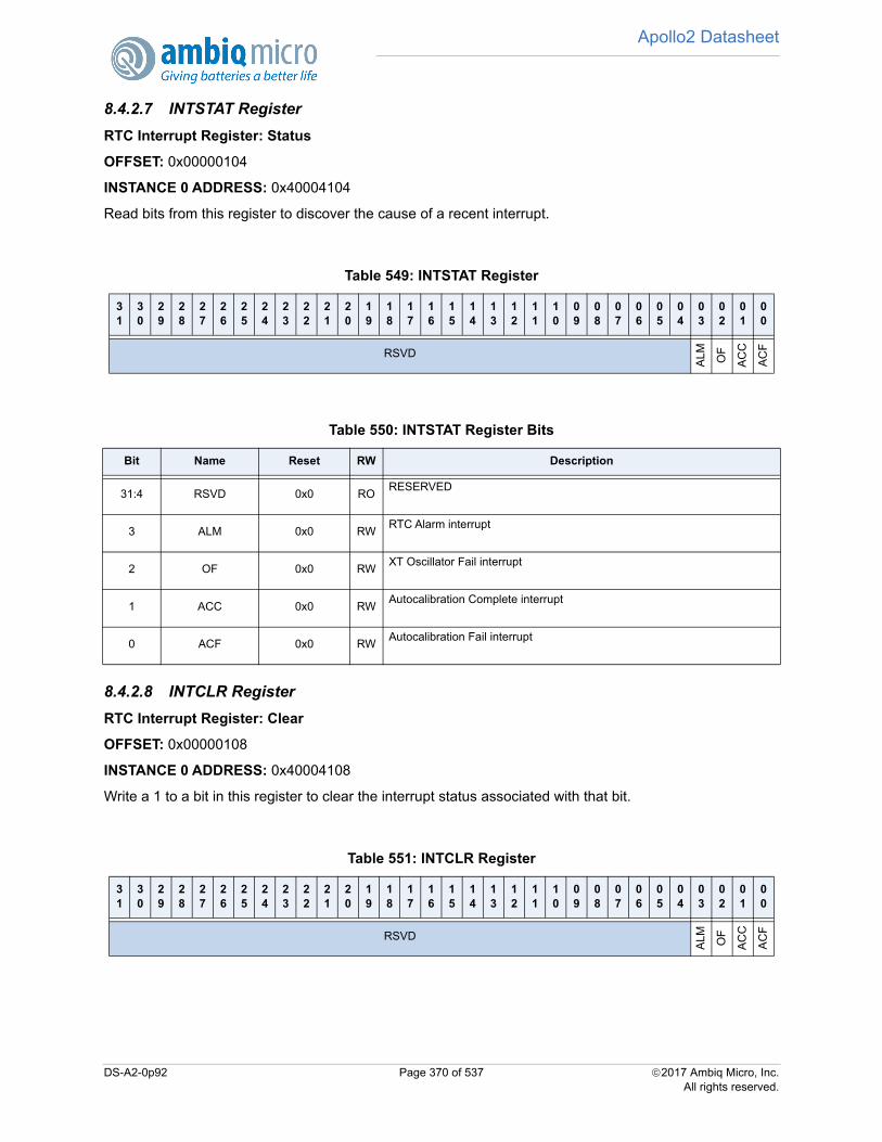
Apollo2 Datasheet
8.4.2.7 INTSTAT Register
RTC Interrupt Register: Status
OFFSET: 0x00000104
INSTANCE 0 ADDRESS: 0x40004104
Read bits from this register to discover the cause of a recent interrupt.
8.4.2.8 INTCLR Register
RTC Interrupt Register: Clear
OFFSET: 0x00000108
INSTANCE 0 ADDRESS: 0x40004108
Write a 1 to a bit in this register to clear the interrupt status associated with that bit.
Table 549: INTSTAT Register
31
30
29
28
27
26
25
24
23
22
21
20
19
18
17
16
15
14
13
12
11
10
09
08
07
06
05
04
03
02
01
00
RSVD
ALM OF
AC
C
AC
F
Table 550: INTSTAT Register Bits
Bit Name Reset RW Description
31:4 RSVD 0x0 RORESERVED
3 ALM 0x0 RWRTC Alarm interrupt
2 OF 0x0 RWXT Oscillator Fail interrupt
1 ACC 0x0 RWAutocalibration Complete interrupt
0 ACF 0x0 RWAutocalibration Fail interrupt
Table 551: INTCLR Register
31
30
29
28
27
26
25
24
23
22
21
20
19
18
17
16
15
14
13
12
11
10
09
08
07
06
05
04
03
02
01
00
RSVD
ALM OF
AC
C
AC
F
DS-A2-0p92 Page 370 of 537 2017 Ambiq Micro, Inc.All rights reserved.
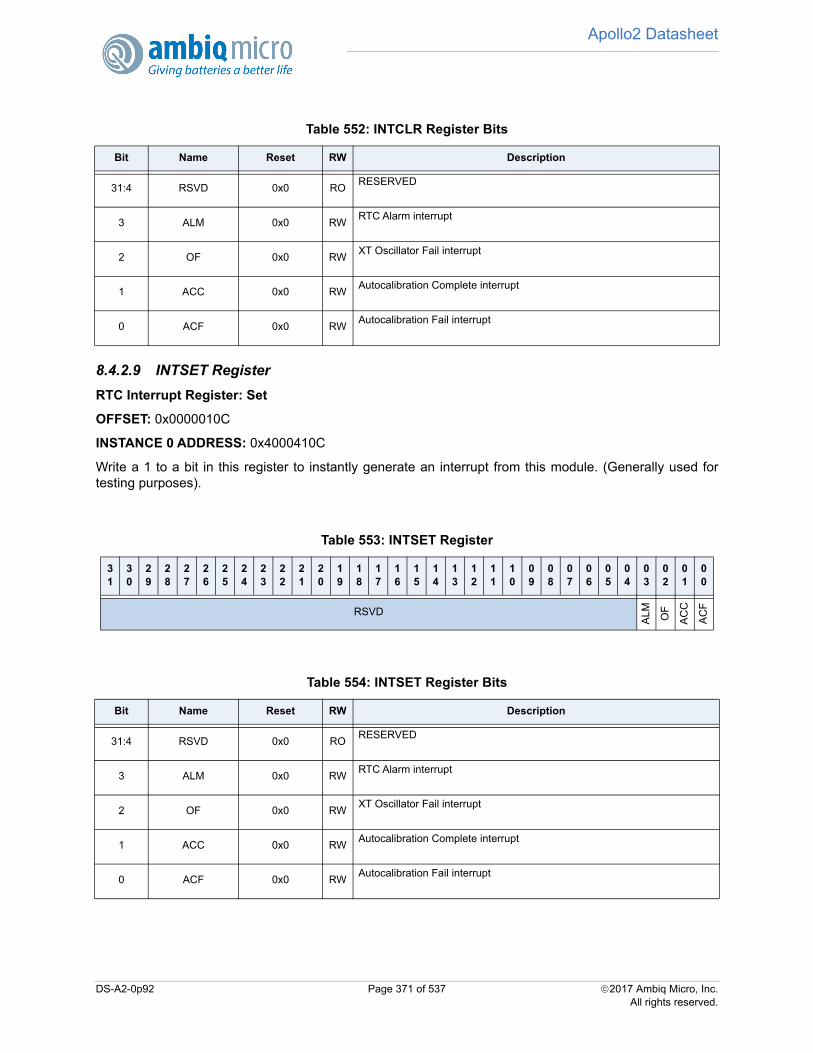
Apollo2 Datasheet
8.4.2.9 INTSET Register
RTC Interrupt Register: Set
OFFSET: 0x0000010C
INSTANCE 0 ADDRESS: 0x4000410C
Write a 1 to a bit in this register to instantly generate an interrupt from this module. (Generally used fortesting purposes).
Table 552: INTCLR Register Bits
Bit Name Reset RW Description
31:4 RSVD 0x0 RORESERVED
3 ALM 0x0 RWRTC Alarm interrupt
2 OF 0x0 RWXT Oscillator Fail interrupt
1 ACC 0x0 RWAutocalibration Complete interrupt
0 ACF 0x0 RWAutocalibration Fail interrupt
Table 553: INTSET Register
31
30
29
28
27
26
25
24
23
22
21
20
19
18
17
16
15
14
13
12
11
10
09
08
07
06
05
04
03
02
01
00
RSVD
ALM OF
AC
C
AC
F
Table 554: INTSET Register Bits
Bit Name Reset RW Description
31:4 RSVD 0x0 RORESERVED
3 ALM 0x0 RWRTC Alarm interrupt
2 OF 0x0 RWXT Oscillator Fail interrupt
1 ACC 0x0 RWAutocalibration Complete interrupt
0 ACF 0x0 RWAutocalibration Fail interrupt
DS-A2-0p92 Page 371 of 537 2017 Ambiq Micro, Inc.All rights reserved.
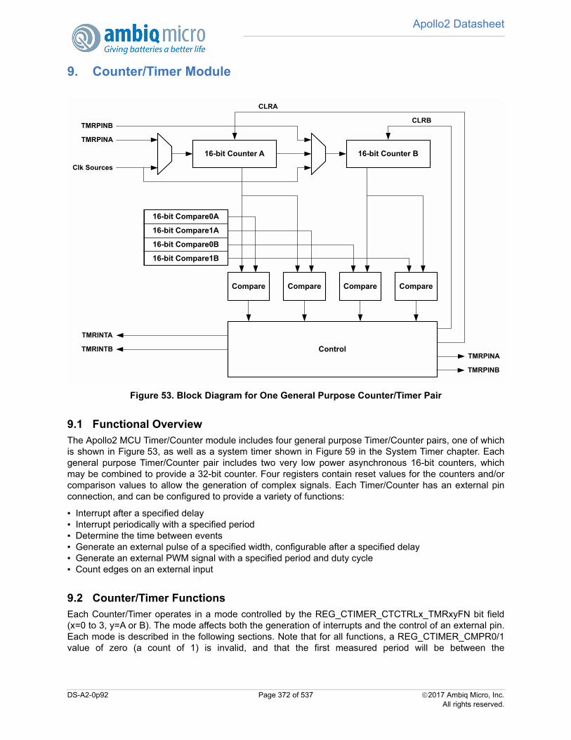
Apollo2 Datasheet
9. Counter/Timer Module
Figure 53. Block Diagram for One General Purpose Counter/Timer Pair
9.1 Functional OverviewThe Apollo2 MCU Timer/Counter module includes four general purpose Timer/Counter pairs, one of whichis shown in Figure 53, as well as a system timer shown in Figure 59 in the System Timer chapter. Eachgeneral purpose Timer/Counter pair includes two very low power asynchronous 16-bit counters, whichmay be combined to provide a 32-bit counter. Four registers contain reset values for the counters and/orcomparison values to allow the generation of complex signals. Each Timer/Counter has an external pinconnection, and can be configured to provide a variety of functions:
Interrupt after a specified delay Interrupt periodically with a specified period Determine the time between events Generate an external pulse of a specified width, configurable after a specified delay Generate an external PWM signal with a specified period and duty cycle Count edges on an external input
9.2 Counter/Timer FunctionsEach Counter/Timer operates in a mode controlled by the REG_CTIMER_CTCTRLx_TMRxyFN bit field(x=0 to 3, y=A or B). The mode affects both the generation of interrupts and the control of an external pin.Each mode is described in the following sections. Note that for all functions, a REG_CTIMER_CMPR0/1value of zero (a count of 1) is invalid, and that the first measured period will be between the
16-bit Counter A 16-bit Counter B
TMRPINA
Clk Sources
16-bit Compare0A
16-bit Compare1B
16-bit Compare0B
16-bit Compare1A
Compare Compare
ControlTMRPINA
TMRINTA
TMRPINB
Compare Compare
TMRPINB
TMRINTB
CLRA
CLRB
DS-A2-0p92 Page 372 of 537 2017 Ambiq Micro, Inc.All rights reserved.
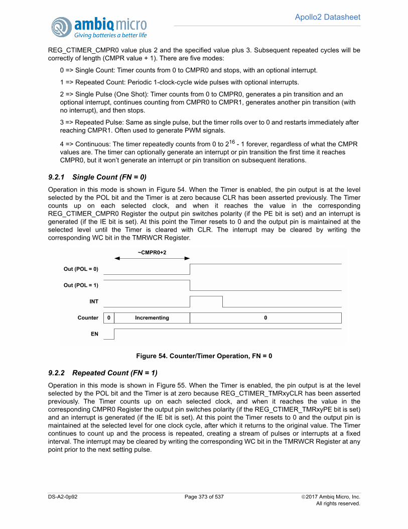
Apollo2 Datasheet
REG_CTIMER_CMPR0 value plus 2 and the specified value plus 3. Subsequent repeated cycles will becorrectly of length (CMPR value + 1). There are five modes:
0 => Single Count: Timer counts from 0 to CMPR0 and stops, with an optional interrupt.
1 => Repeated Count: Periodic 1-clock-cycle wide pulses with optional interrupts.
2 => Single Pulse (One Shot): Timer counts from 0 to CMPR0, generates a pin transition and an optional interrupt, continues counting from CMPR0 to CMPR1, generates another pin transition (with no interrupt), and then stops.
3 => Repeated Pulse: Same as single pulse, but the timer rolls over to 0 and restarts immediately after reaching CMPR1. Often used to generate PWM signals.
4 => Continuous: The timer repeatedly counts from 0 to 216 - 1 forever, regardless of what the CMPR values are. The timer can optionally generate an interrupt or pin transition the first time it reaches CMPR0, but it won’t generate an interrupt or pin transition on subsequent iterations.
9.2.1 Single Count (FN = 0)
Operation in this mode is shown in Figure 54. When the Timer is enabled, the pin output is at the levelselected by the POL bit and the Timer is at zero because CLR has been asserted previously. The Timercounts up on each selected clock, and when it reaches the value in the correspondingREG_CTIMER_CMPR0 Register the output pin switches polarity (if the PE bit is set) and an interrupt isgenerated (if the IE bit is set). At this point the Timer resets to 0 and the output pin is maintained at theselected level until the Timer is cleared with CLR. The interrupt may be cleared by writing thecorresponding WC bit in the TMRWCR Register.
Figure 54. Counter/Timer Operation, FN = 0
9.2.2 Repeated Count (FN = 1)
Operation in this mode is shown in Figure 55. When the Timer is enabled, the pin output is at the levelselected by the POL bit and the Timer is at zero because REG_CTIMER_TMRxyCLR has been assertedpreviously. The Timer counts up on each selected clock, and when it reaches the value in thecorresponding CMPR0 Register the output pin switches polarity (if the REG_CTIMER_TMRxyPE bit is set)and an interrupt is generated (if the IE bit is set). At this point the Timer resets to 0 and the output pin ismaintained at the selected level for one clock cycle, after which it returns to the original value. The Timercontinues to count up and the process is repeated, creating a stream of pulses or interrupts at a fixedinterval. The interrupt may be cleared by writing the corresponding WC bit in the TMRWCR Register at anypoint prior to the next setting pulse.
Out (POL = 0)
Out (POL = 1)
INT
Counter
EN
0 Incrementing 0
~CMPR0+2
DS-A2-0p92 Page 373 of 537 2017 Ambiq Micro, Inc.All rights reserved.
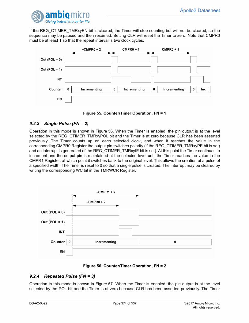
Apollo2 Datasheet
If the REG_CTIMER_TMRxyEN bit is cleared, the Timer will stop counting but will not be cleared, so thesequence may be paused and then resumed. Setting CLR will reset the Timer to zero. Note that CMPR0must be at least 1 so that the repeat interval is two clock cycles.
Figure 55. Counter/Timer Operation, FN = 1
9.2.3 Single Pulse (FN = 2)
Operation in this mode is shown in Figure 56. When the Timer is enabled, the pin output is at the levelselected by the REG_CTIMER_TMRxyPOL bit and the Timer is at zero because CLR has been assertedpreviously. The Timer counts up on each selected clock, and when it reaches the value in thecorresponding CMPR0 Register the output pin switches polarity (if the REG_CTIMER_TMRxyPE bit is set)and an interrupt is generated (if the REG_CTIMER_TMRxyIE bit is set). At this point the Timer continues toincrement and the output pin is maintained at the selected level until the Timer reaches the value in theCMPR1 Register, at which point it switches back to the original level. This allows the creation of a pulse ofa specified width. The Timer is reset to 0 so that a single pulse is created. The interrupt may be cleared bywriting the corresponding WC bit in the TMRWCR Register.
Figure 56. Counter/Timer Operation, FN = 2
9.2.4 Repeated Pulse (FN = 3)
Operation in this mode is shown in Figure 57. When the Timer is enabled, the pin output is at the levelselected by the POL bit and the Timer is at zero because CLR has been asserted previously. The Timer
Out (POL = 0)
Out (POL = 1)
INT
Counter
EN
0 Incrementing 0
~CMPR0 + 2 CMPR0 + 1 CMPR0 + 1
Incrementing 0 Incrementing 0 Inc
Out (POL = 0)
Out (POL = 1)
INT
Counter
EN
0 Incrementing 0
~CMPR0 + 2
~CMPR1 + 2
DS-A2-0p92 Page 374 of 537 2017 Ambiq Micro, Inc.All rights reserved.
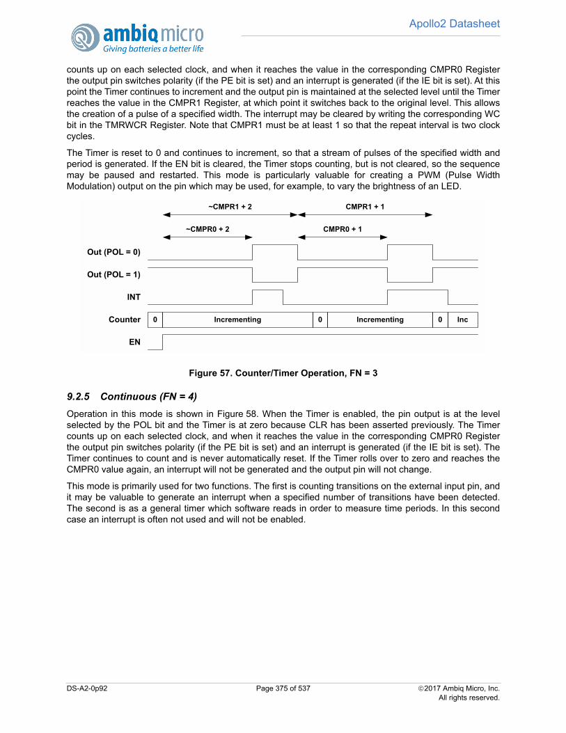
Apollo2 Datasheet
counts up on each selected clock, and when it reaches the value in the corresponding CMPR0 Registerthe output pin switches polarity (if the PE bit is set) and an interrupt is generated (if the IE bit is set). At thispoint the Timer continues to increment and the output pin is maintained at the selected level until the Timerreaches the value in the CMPR1 Register, at which point it switches back to the original level. This allowsthe creation of a pulse of a specified width. The interrupt may be cleared by writing the corresponding WCbit in the TMRWCR Register. Note that CMPR1 must be at least 1 so that the repeat interval is two clockcycles.
The Timer is reset to 0 and continues to increment, so that a stream of pulses of the specified width andperiod is generated. If the EN bit is cleared, the Timer stops counting, but is not cleared, so the sequencemay be paused and restarted. This mode is particularly valuable for creating a PWM (Pulse WidthModulation) output on the pin which may be used, for example, to vary the brightness of an LED.
Figure 57. Counter/Timer Operation, FN = 3
9.2.5 Continuous (FN = 4)
Operation in this mode is shown in Figure 58. When the Timer is enabled, the pin output is at the levelselected by the POL bit and the Timer is at zero because CLR has been asserted previously. The Timercounts up on each selected clock, and when it reaches the value in the corresponding CMPR0 Registerthe output pin switches polarity (if the PE bit is set) and an interrupt is generated (if the IE bit is set). TheTimer continues to count and is never automatically reset. If the Timer rolls over to zero and reaches theCMPR0 value again, an interrupt will not be generated and the output pin will not change.
This mode is primarily used for two functions. The first is counting transitions on the external input pin, andit may be valuable to generate an interrupt when a specified number of transitions have been detected.The second is as a general timer which software reads in order to measure time periods. In this secondcase an interrupt is often not used and will not be enabled.
Out (POL = 0)
Out (POL = 1)
INT
Counter
EN
0 Incrementing 0
~CMPR0 + 2
~CMPR1 + 2
CMPR0 + 1
CMPR1 + 1
Incrementing 0 Inc
DS-A2-0p92 Page 375 of 537 2017 Ambiq Micro, Inc.All rights reserved.

Apollo2 Datasheet
Figure 58. Counter/Timer Operation, FN = 4
9.3 Creating 32-bit CountersEach pair (A/B) of 16-bit counters may be combined to create a 32-bit counter. This configuration iscreated by setting the REG_CTIMER_CTCTRLx_CTRLINKx bit for the pair. The control bits for the Acounter of the pair are used to control the 32-bit counter, and the B control bits are ignored. The CMPR0and CMPR1 registers for each 16-bit counter are concatenated to provide the 32-bit comparison values,and all timer modes are supported.
9.4 Power Optimization by Measuring HCLKEach timer has the capability to select the processor clock HCLK as the counter clock input. This allows avery straightforward measurement of how much of the time the processor is in a Sleep or Deep Sleepmode. Two counters are configured with FN = 4 so that they count continuously. One is supplied HCLK asits clock, and the other is supplied with a divided version of the HFRC clock. The two counters are enabledsimultaneously, and after some period of system operation they are disabled and read. The HFRC countvalue defines how much real time has elapsed and how many HCLKs could have occurred in that time,and the HCLK count value defines how many actual HCLKs were received in that time. The ratio is anaccurate measurement of the percentage of time the CPU is asleep, and is an effective tool for poweroptimization.
9.5 Generating the Sample Rate for the ADCTimer CTTMRA3 has a special function which allows it to be used as the sample trigger generator for theADC. If the ADCEN and TMRA3PE bits are set, the output of the timer is sent to the ADC which uses it asa trigger. Note that, while the TMRA3PE bit must be set, the TCTA3 GPIO output for the Ctimer should notbe enabled to prevent unexpected transitions on the corresponding package pin.
Typically, Ctimer3 is configured in Repeated Count (FN =1) mode. TMRA3IE may be set to generate aninterrupt whenever the trigger occurs, but typically the ADC interrupt will be used for this purpose.
9.6 Measuring Buck Converter Charge InsertionEach counter may be connected to a pulse stream from one of the two Buck Converters. One pulse isgenerated each time the Buck Converter delivers charge onto the capacitor, and therefore the number ofpulses is a good indication of the amount of energy used by the corresponding power domain in aparticular time period. Two counters are configured with FN = 4 so that they count continuously. One issupplied a Buck Converter pulse stream as its clock, and the other is supplied with a divided version of theLFRC clock to avoid creating extra power consumption due to the power measurement. The two countersare enabled simultaneously, and after some period of system operation they are disabled and read. The
Out (POL = 0)
Out (POL = 1)
INT
Counter
EN
0 Incrementing
~CMPR0 + 2
DS-A2-0p92 Page 376 of 537 2017 Ambiq Micro, Inc.All rights reserved.
Apollo2 Datasheet
LFRC count value defines how much real time has elapsed, and the Buck Converter count value defineshow much energy was consumed in that time
9.7 CTIMER RegistersCounter/Timer
INSTANCE 0 BASE ADDRESS:0x40008000
The Counter/Timer block contains 8 sixteen bit counter or timer functions. Each pair of these counters canbe cascaded into 32 bit Counter/Timer functions.
9.7.1 Register Memory Map
Table 555: CTIMER Register Map
Address(s) Register Name Description
0x40008000 TMR0 Counter/Timer Register
0x40008004 CMPRA0 Counter/Timer A0 Compare Registers
0x40008008 CMPRB0 Counter/Timer B0 Compare Registers
0x4000800C CTRL0 Counter/Timer Control
0x40008010 TMR1 Counter/Timer Register
0x40008014 CMPRA1 Counter/Timer A1 Compare Registers
0x40008018 CMPRB1 Counter/Timer B1 Compare Registers
0x4000801C CTRL1 Counter/Timer Control
0x40008020 TMR2 Counter/Timer Register
0x40008024 CMPRA2 Counter/Timer A2 Compare Registers
0x40008028 CMPRB2 Counter/Timer B2 Compare Registers
0x4000802C CTRL2 Counter/Timer Control
0x40008030 TMR3 Counter/Timer Register
0x40008034 CMPRA3 Counter/Timer A3 Compare Registers
0x40008038 CMPRB3 Counter/Timer B3 Compare Registers
0x4000803C CTRL3 Counter/Timer Control
0x40008200 INTEN Counter/Timer Interrupts: Enable
0x40008204 INTSTAT Counter/Timer Interrupts: Status
0x40008208 INTCLR Counter/Timer Interrupts: Clear
0x4000820C INTSET Counter/Timer Interrupts: Set
DS-A2-0p92 Page 377 of 537 2017 Ambiq Micro, Inc.All rights reserved.
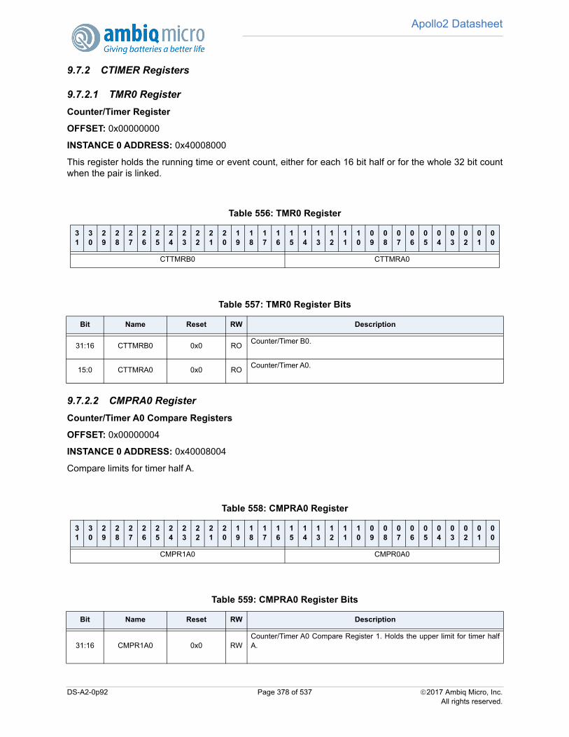
Apollo2 Datasheet
9.7.2 CTIMER Registers
9.7.2.1 TMR0 Register
Counter/Timer Register
OFFSET: 0x00000000
INSTANCE 0 ADDRESS: 0x40008000
This register holds the running time or event count, either for each 16 bit half or for the whole 32 bit countwhen the pair is linked.
9.7.2.2 CMPRA0 Register
Counter/Timer A0 Compare Registers
OFFSET: 0x00000004
INSTANCE 0 ADDRESS: 0x40008004
Compare limits for timer half A.
Table 556: TMR0 Register
31
30
29
28
27
26
25
24
23
22
21
20
19
18
17
16
15
14
13
12
11
10
09
08
07
06
05
04
03
02
01
00
CTTMRB0 CTTMRA0
Table 557: TMR0 Register Bits
Bit Name Reset RW Description
31:16 CTTMRB0 0x0 ROCounter/Timer B0.
15:0 CTTMRA0 0x0 ROCounter/Timer A0.
Table 558: CMPRA0 Register
31
30
29
28
27
26
25
24
23
22
21
20
19
18
17
16
15
14
13
12
11
10
09
08
07
06
05
04
03
02
01
00
CMPR1A0 CMPR0A0
Table 559: CMPRA0 Register Bits
Bit Name Reset RW Description
31:16 CMPR1A0 0x0 RWCounter/Timer A0 Compare Register 1. Holds the upper limit for timer halfA.
DS-A2-0p92 Page 378 of 537 2017 Ambiq Micro, Inc.All rights reserved.
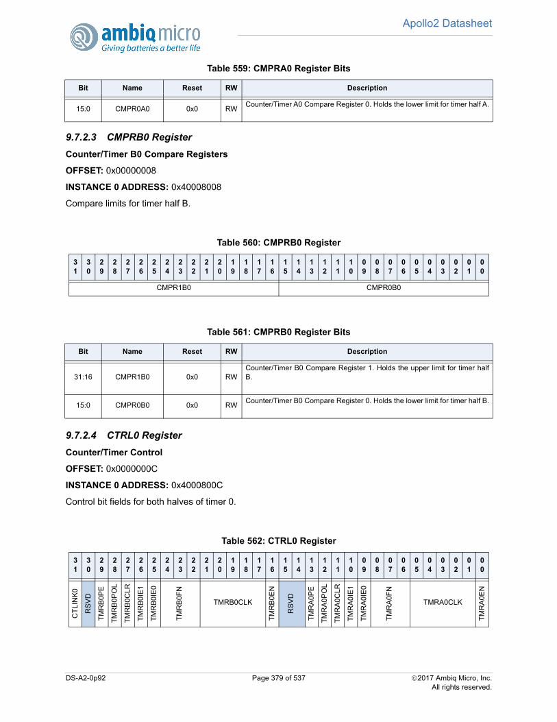
Apollo2 Datasheet
9.7.2.3 CMPRB0 Register
Counter/Timer B0 Compare Registers
OFFSET: 0x00000008
INSTANCE 0 ADDRESS: 0x40008008
Compare limits for timer half B.
9.7.2.4 CTRL0 Register
Counter/Timer Control
OFFSET: 0x0000000C
INSTANCE 0 ADDRESS: 0x4000800C
Control bit fields for both halves of timer 0.
15:0 CMPR0A0 0x0 RWCounter/Timer A0 Compare Register 0. Holds the lower limit for timer half A.
Table 560: CMPRB0 Register
31
30
29
28
27
26
25
24
23
22
21
20
19
18
17
16
15
14
13
12
11
10
09
08
07
06
05
04
03
02
01
00
CMPR1B0 CMPR0B0
Table 561: CMPRB0 Register Bits
Bit Name Reset RW Description
31:16 CMPR1B0 0x0 RWCounter/Timer B0 Compare Register 1. Holds the upper limit for timer halfB.
15:0 CMPR0B0 0x0 RWCounter/Timer B0 Compare Register 0. Holds the lower limit for timer half B.
Table 562: CTRL0 Register
31
30
29
28
27
26
25
24
23
22
21
20
19
18
17
16
15
14
13
12
11
10
09
08
07
06
05
04
03
02
01
00
CT
LIN
K0
RS
VD
TM
RB
0PE
TM
RB
0PO
L
TM
RB
0CLR
TM
RB
0IE
1
TM
RB
0IE
0
TM
RB
0FN
TMRB0CLK
TM
RB
0EN
RS
VD
TM
RA
0PE
TM
RA
0PO
L
TM
RA
0CLR
TM
RA
0IE
1
TM
RA
0IE
0
TM
RA
0FN
TMRA0CLK
TM
RA
0EN
Table 559: CMPRA0 Register Bits
Bit Name Reset RW Description
DS-A2-0p92 Page 379 of 537 2017 Ambiq Micro, Inc.All rights reserved.

Apollo2 Datasheet
Table 563: CTRL0 Register Bits
Bit Name Reset RW Description
31 CTLINK0 0x0 RW
Counter/Timer A0/B0 Link bit.
TWO_16BIT_TIMERS = 0x0 - Use A0/B0 timers as two independent 16-bittimers (default).32BIT_TIMER = 0x1 - Link A0/B0 timers into a single 32-bit timer.
30 RSVD 0x0 RORESERVED
29 TMRB0PE 0x0 RW
Counter/Timer B0 Output Enable bit.
DIS = 0x0 - Counter/Timer B holds the TMRPINB signal at the valueTMRB0POL.EN = 0x1 - Enable counter/timer B0 to generate a signal on TMRPINB.
28 TMRB0POL 0x0 RW
Counter/Timer B0 output polarity.
NORMAL = 0x0 - The polarity of the TMRPINB0 pin is the same as the timeroutput.INVERTED = 0x1 - The polarity of the TMRPINB0 pin is the inverse of thetimer output.
27 TMRB0CLR 0x0 RW
Counter/Timer B0 Clear bit.
RUN = 0x0 - Allow counter/timer B0 to runCLEAR = 0x1 - Holds counter/timer B0 at 0x0000.
26 TMRB0IE1 0x0 RW
Counter/Timer B0 Interrupt Enable bit for COMPR1.
DIS = 0x0 - Disable counter/timer B0 from generating an interrupt based onCOMPR1.EN = 0x1 - Enable counter/timer B0 to generate an interrupt based on COM-PR1.
25 TMRB0IE0 0x0 RW
Counter/Timer B0 Interrupt Enable bit for COMPR0.
DIS = 0x0 - Disable counter/timer B0 from generating an interrupt based onCOMPR0.EN = 0x1 - Enable counter/timer B0 to generate an interrupt based on COM-PR0
24:22 TMRB0FN 0x0 RW
Counter/Timer B0 Function Select.
SINGLECOUNT = 0x0 - Single count (output toggles and sticks). Count toCMPR0B0, stop.REPEATEDCOUNT = 0x1 - Repeated count (periodic 1-clock-cycle-widepulses). Count to CMPR0B0, restart.PULSE_ONCE = 0x2 - Pulse once (aka one-shot). Count to CMPR0B0,assert, count to CMPR1B0, deassert, stop.PULSE_CONT = 0x3 - Pulse continously. Count to CMPR0B0, assert,count to CMPR1B0, deassert, restart.CONTINUOUS = 0x4 - Continuous run (aka Free Run). Count continuously.
DS-A2-0p92 Page 380 of 537 2017 Ambiq Micro, Inc.All rights reserved.
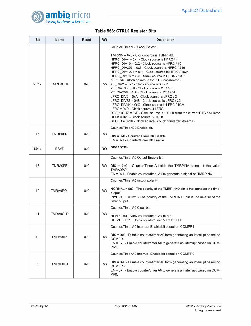
Apollo2 Datasheet
21:17 TMRB0CLK 0x0 RW
Counter/Timer B0 Clock Select.
TMRPIN = 0x0 - Clock source is TMRPINB.HFRC_DIV4 = 0x1 - Clock source is HFRC / 4HFRC_DIV16 = 0x2 - Clock source is HFRC / 16HFRC_DIV256 = 0x3 - Clock source is HFRC / 256HFRC_DIV1024 = 0x4 - Clock source is HFRC / 1024HFRC_DIV4K = 0x5 - Clock source is HFRC / 4096XT = 0x6 - Clock source is the XT (uncalibrated).XT_DIV2 = 0x7 - Clock source is XT / 2XT_DIV16 = 0x8 - Clock source is XT / 16XT_DIV256 = 0x9 - Clock source is XT / 256LFRC_DIV2 = 0xA - Clock source is LFRC / 2LFRC_DIV32 = 0xB - Clock source is LFRC / 32LFRC_DIV1K = 0xC - Clock source is LFRC / 1024LFRC = 0xD - Clock source is LFRCRTC_100HZ = 0xE - Clock source is 100 Hz from the current RTC oscillator.HCLK = 0xF - Clock source is HCLK.BUCKB = 0x10 - Clock source is buck converter stream B.
16 TMRB0EN 0x0 RW
Counter/Timer B0 Enable bit.
DIS = 0x0 - Counter/Timer B0 Disable.EN = 0x1 - Counter/Timer B0 Enable.
15:14 RSVD 0x0 RORESERVED
13 TMRA0PE 0x0 RW
Counter/Timer A0 Output Enable bit.
DIS = 0x0 - Counter/Timer A holds the TMRPINA signal at the valueTMRA0POL.EN = 0x1 - Enable counter/timer A0 to generate a signal on TMRPINA.
12 TMRA0POL 0x0 RW
Counter/Timer A0 output polarity.
NORMAL = 0x0 - The polarity of the TMRPINA0 pin is the same as the timeroutput.INVERTED = 0x1 - The polarity of the TMRPINA0 pin is the inverse of thetimer output.
11 TMRA0CLR 0x0 RW
Counter/Timer A0 Clear bit.
RUN = 0x0 - Allow counter/timer A0 to runCLEAR = 0x1 - Holds counter/timer A0 at 0x0000.
10 TMRA0IE1 0x0 RW
Counter/Timer A0 Interrupt Enable bit based on COMPR1.
DIS = 0x0 - Disable counter/timer A0 from generating an interrupt based onCOMPR1.EN = 0x1 - Enable counter/timer A0 to generate an interrupt based on COM-PR1.
9 TMRA0IE0 0x0 RW
Counter/Timer A0 Interrupt Enable bit based on COMPR0.
DIS = 0x0 - Disable counter/timer A0 from generating an interrupt based onCOMPR0.EN = 0x1 - Enable counter/timer A0 to generate an interrupt based on COM-PR0.
Table 563: CTRL0 Register Bits
Bit Name Reset RW Description
DS-A2-0p92 Page 381 of 537 2017 Ambiq Micro, Inc.All rights reserved.

Apollo2 Datasheet
9.7.2.5 TMR1 Register
Counter/Timer Register
OFFSET: 0x00000010
INSTANCE 0 ADDRESS: 0x40008010
This register holds the running time or event count, either for each 16 bit half or for the whole 32 bit countwhen the pair is linked.
8:6 TMRA0FN 0x0 RW
Counter/Timer A0 Function Select.
SINGLECOUNT = 0x0 - Single count (output toggles and sticks). Count toCMPR0A0, stop.REPEATEDCOUNT = 0x1 - Repeated count (periodic 1-clock-cycle-widepulses). Count to CMPR0A0, restart.PULSE_ONCE = 0x2 - Pulse once (aka one-shot). Count to CMPR0A0,assert, count to CMPR1A0, deassert, stop.PULSE_CONT = 0x3 - Pulse continously. Count to CMPR0A0, assert,count to CMPR1A0, deassert, restart.CONTINUOUS = 0x4 - Continuous run (aka Free Run). Count continuously.
5:1 TMRA0CLK 0x0 RW
Counter/Timer A0 Clock Select.
TMRPIN = 0x0 - Clock source is TMRPINA.HFRC_DIV4 = 0x1 - Clock source is HFRC / 4HFRC_DIV16 = 0x2 - Clock source is HFRC / 16HFRC_DIV256 = 0x3 - Clock source is HFRC / 256HFRC_DIV1024 = 0x4 - Clock source is HFRC / 1024HFRC_DIV4K = 0x5 - Clock source is HFRC / 4096XT = 0x6 - Clock source is the XT (uncalibrated).XT_DIV2 = 0x7 - Clock source is XT / 2XT_DIV16 = 0x8 - Clock source is XT / 16XT_DIV256 = 0x9 - Clock source is XT / 256LFRC_DIV2 = 0xA - Clock source is LFRC / 2LFRC_DIV32 = 0xB - Clock source is LFRC / 32LFRC_DIV1K = 0xC - Clock source is LFRC / 1024LFRC = 0xD - Clock source is LFRCRTC_100HZ = 0xE - Clock source is 100 Hz from the current RTC oscillator.HCLK_DIV4 = 0xF - Clock source is HCLK / 4.BUCKA = 0x10 - Clock source is buck converter stream A.
0 TMRA0EN 0x0 RW
Counter/Timer A0 Enable bit.
DIS = 0x0 - Counter/Timer A0 Disable.EN = 0x1 - Counter/Timer A0 Enable.
Table 564: TMR1 Register
31
30
29
28
27
26
25
24
23
22
21
20
19
18
17
16
15
14
13
12
11
10
09
08
07
06
05
04
03
02
01
00
CTTMRB1 CTTMRA1
Table 563: CTRL0 Register Bits
Bit Name Reset RW Description
DS-A2-0p92 Page 382 of 537 2017 Ambiq Micro, Inc.All rights reserved.
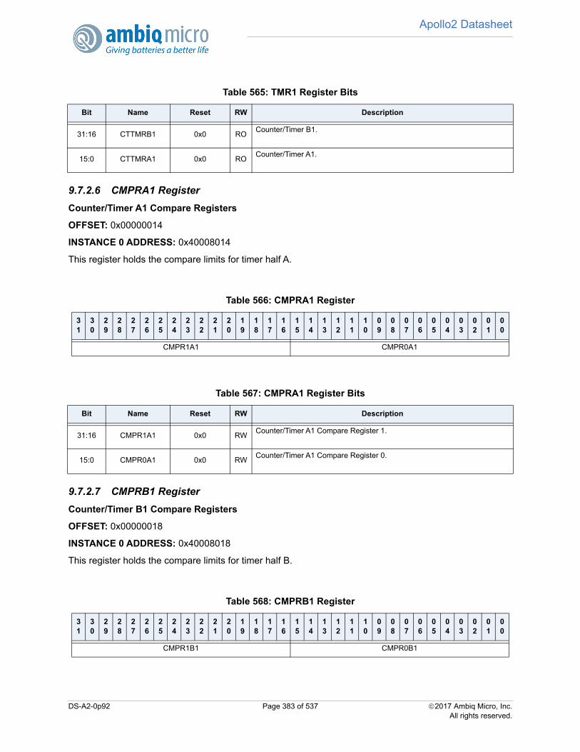
Apollo2 Datasheet
9.7.2.6 CMPRA1 Register
Counter/Timer A1 Compare Registers
OFFSET: 0x00000014
INSTANCE 0 ADDRESS: 0x40008014
This register holds the compare limits for timer half A.
9.7.2.7 CMPRB1 Register
Counter/Timer B1 Compare Registers
OFFSET: 0x00000018
INSTANCE 0 ADDRESS: 0x40008018
This register holds the compare limits for timer half B.
Table 565: TMR1 Register Bits
Bit Name Reset RW Description
31:16 CTTMRB1 0x0 ROCounter/Timer B1.
15:0 CTTMRA1 0x0 ROCounter/Timer A1.
Table 566: CMPRA1 Register
31
30
29
28
27
26
25
24
23
22
21
20
19
18
17
16
15
14
13
12
11
10
09
08
07
06
05
04
03
02
01
00
CMPR1A1 CMPR0A1
Table 567: CMPRA1 Register Bits
Bit Name Reset RW Description
31:16 CMPR1A1 0x0 RWCounter/Timer A1 Compare Register 1.
15:0 CMPR0A1 0x0 RWCounter/Timer A1 Compare Register 0.
Table 568: CMPRB1 Register
31
30
29
28
27
26
25
24
23
22
21
20
19
18
17
16
15
14
13
12
11
10
09
08
07
06
05
04
03
02
01
00
CMPR1B1 CMPR0B1
DS-A2-0p92 Page 383 of 537 2017 Ambiq Micro, Inc.All rights reserved.
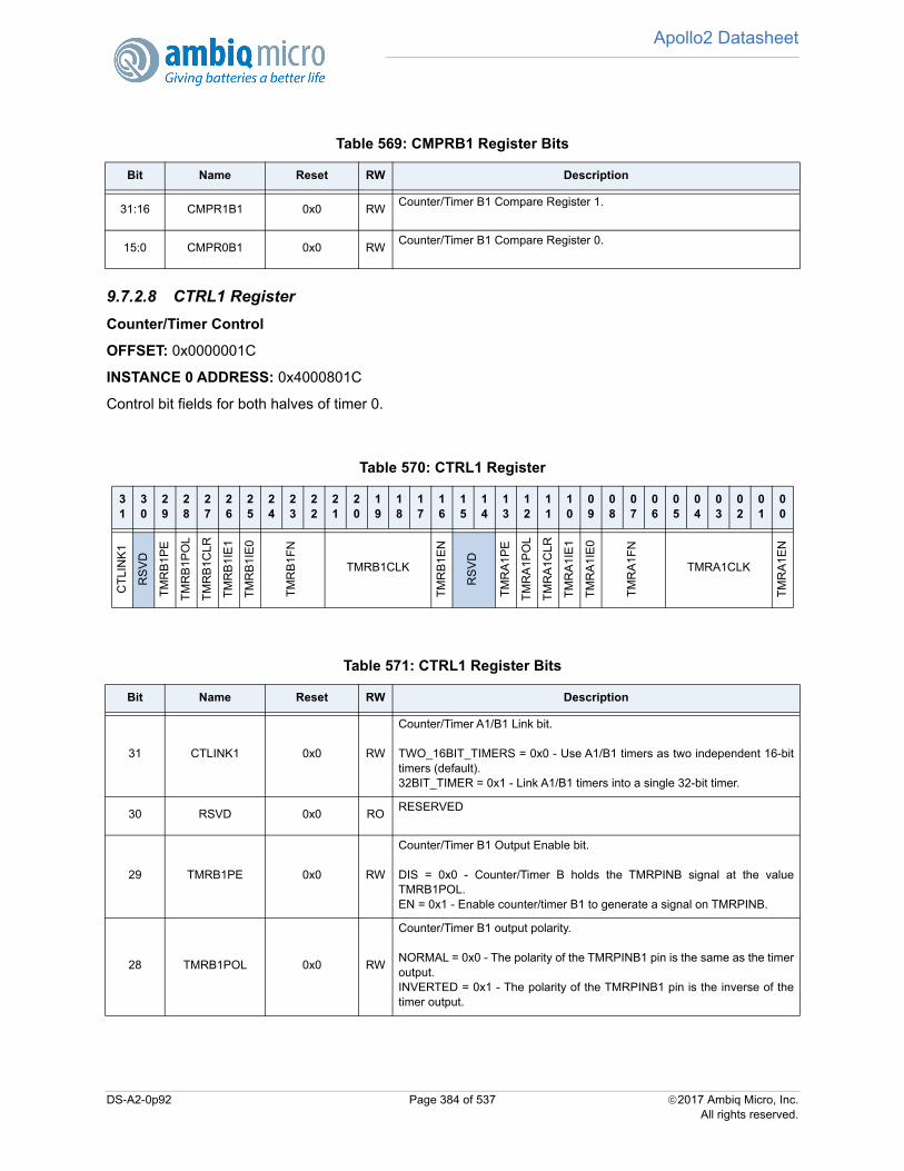
Apollo2 Datasheet
9.7.2.8 CTRL1 Register
Counter/Timer Control
OFFSET: 0x0000001C
INSTANCE 0 ADDRESS: 0x4000801C
Control bit fields for both halves of timer 0.
Table 569: CMPRB1 Register Bits
Bit Name Reset RW Description
31:16 CMPR1B1 0x0 RWCounter/Timer B1 Compare Register 1.
15:0 CMPR0B1 0x0 RWCounter/Timer B1 Compare Register 0.
Table 570: CTRL1 Register
31
30
29
28
27
26
25
24
23
22
21
20
19
18
17
16
15
14
13
12
11
10
09
08
07
06
05
04
03
02
01
00
CT
LIN
K1
RS
VD
TM
RB
1PE
TM
RB
1PO
L
TM
RB
1CLR
TM
RB
1IE
1
TM
RB
1IE
0
TM
RB
1FN
TMRB1CLK
TM
RB
1EN
RS
VD
TM
RA
1PE
TM
RA
1PO
L
TM
RA
1CLR
TM
RA
1IE
1
TM
RA
1IE
0
TM
RA
1FN
TMRA1CLK
TM
RA
1EN
Table 571: CTRL1 Register Bits
Bit Name Reset RW Description
31 CTLINK1 0x0 RW
Counter/Timer A1/B1 Link bit.
TWO_16BIT_TIMERS = 0x0 - Use A1/B1 timers as two independent 16-bittimers (default).32BIT_TIMER = 0x1 - Link A1/B1 timers into a single 32-bit timer.
30 RSVD 0x0 RORESERVED
29 TMRB1PE 0x0 RW
Counter/Timer B1 Output Enable bit.
DIS = 0x0 - Counter/Timer B holds the TMRPINB signal at the valueTMRB1POL.EN = 0x1 - Enable counter/timer B1 to generate a signal on TMRPINB.
28 TMRB1POL 0x0 RW
Counter/Timer B1 output polarity.
NORMAL = 0x0 - The polarity of the TMRPINB1 pin is the same as the timeroutput.INVERTED = 0x1 - The polarity of the TMRPINB1 pin is the inverse of thetimer output.
DS-A2-0p92 Page 384 of 537 2017 Ambiq Micro, Inc.All rights reserved.
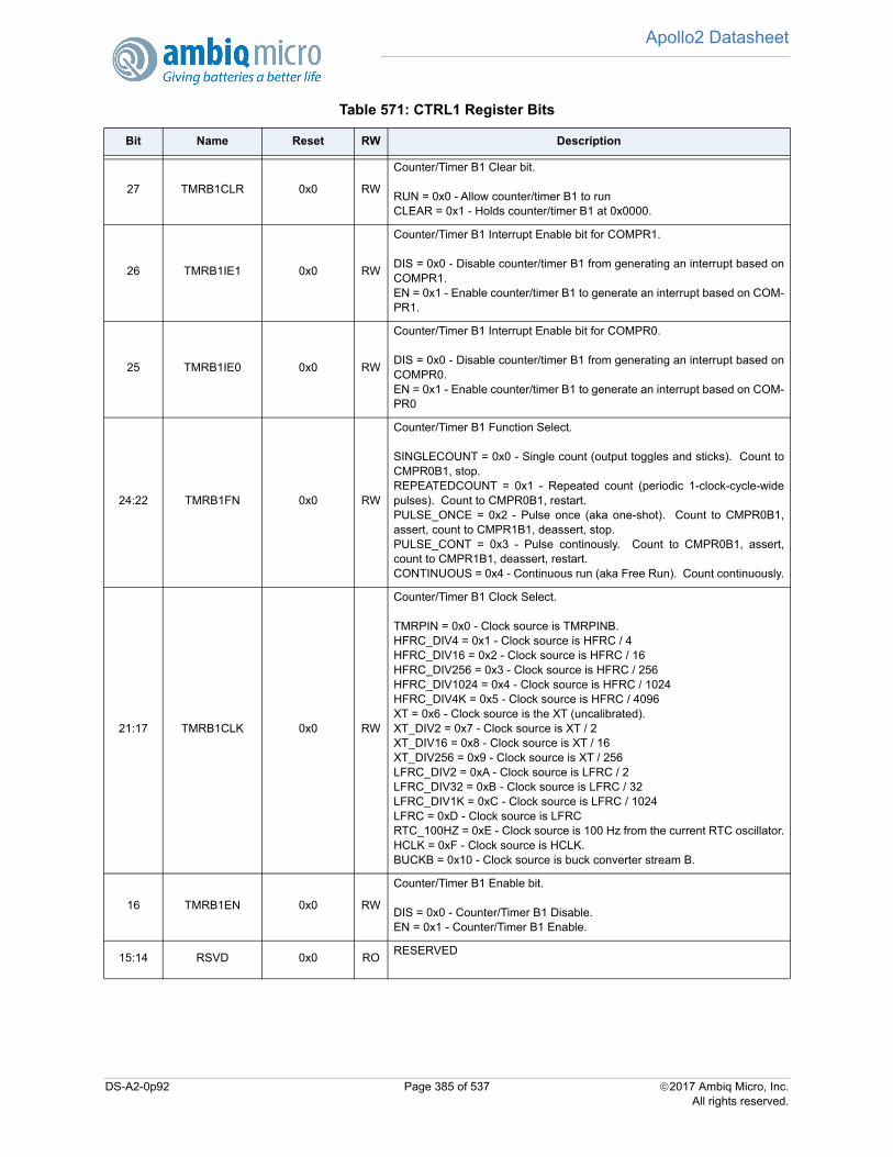
Apollo2 Datasheet
27 TMRB1CLR 0x0 RW
Counter/Timer B1 Clear bit.
RUN = 0x0 - Allow counter/timer B1 to runCLEAR = 0x1 - Holds counter/timer B1 at 0x0000.
26 TMRB1IE1 0x0 RW
Counter/Timer B1 Interrupt Enable bit for COMPR1.
DIS = 0x0 - Disable counter/timer B1 from generating an interrupt based onCOMPR1.EN = 0x1 - Enable counter/timer B1 to generate an interrupt based on COM-PR1.
25 TMRB1IE0 0x0 RW
Counter/Timer B1 Interrupt Enable bit for COMPR0.
DIS = 0x0 - Disable counter/timer B1 from generating an interrupt based onCOMPR0.EN = 0x1 - Enable counter/timer B1 to generate an interrupt based on COM-PR0
24:22 TMRB1FN 0x0 RW
Counter/Timer B1 Function Select.
SINGLECOUNT = 0x0 - Single count (output toggles and sticks). Count toCMPR0B1, stop.REPEATEDCOUNT = 0x1 - Repeated count (periodic 1-clock-cycle-widepulses). Count to CMPR0B1, restart.PULSE_ONCE = 0x2 - Pulse once (aka one-shot). Count to CMPR0B1,assert, count to CMPR1B1, deassert, stop.PULSE_CONT = 0x3 - Pulse continously. Count to CMPR0B1, assert,count to CMPR1B1, deassert, restart.CONTINUOUS = 0x4 - Continuous run (aka Free Run). Count continuously.
21:17 TMRB1CLK 0x0 RW
Counter/Timer B1 Clock Select.
TMRPIN = 0x0 - Clock source is TMRPINB.HFRC_DIV4 = 0x1 - Clock source is HFRC / 4HFRC_DIV16 = 0x2 - Clock source is HFRC / 16HFRC_DIV256 = 0x3 - Clock source is HFRC / 256HFRC_DIV1024 = 0x4 - Clock source is HFRC / 1024HFRC_DIV4K = 0x5 - Clock source is HFRC / 4096XT = 0x6 - Clock source is the XT (uncalibrated).XT_DIV2 = 0x7 - Clock source is XT / 2XT_DIV16 = 0x8 - Clock source is XT / 16XT_DIV256 = 0x9 - Clock source is XT / 256LFRC_DIV2 = 0xA - Clock source is LFRC / 2LFRC_DIV32 = 0xB - Clock source is LFRC / 32LFRC_DIV1K = 0xC - Clock source is LFRC / 1024LFRC = 0xD - Clock source is LFRCRTC_100HZ = 0xE - Clock source is 100 Hz from the current RTC oscillator.HCLK = 0xF - Clock source is HCLK.BUCKB = 0x10 - Clock source is buck converter stream B.
16 TMRB1EN 0x0 RW
Counter/Timer B1 Enable bit.
DIS = 0x0 - Counter/Timer B1 Disable.EN = 0x1 - Counter/Timer B1 Enable.
15:14 RSVD 0x0 RORESERVED
Table 571: CTRL1 Register Bits
Bit Name Reset RW Description
DS-A2-0p92 Page 385 of 537 2017 Ambiq Micro, Inc.All rights reserved.

Apollo2 Datasheet
13 TMRA1PE 0x0 RW
Counter/Timer A1 Output Enable bit.
DIS = 0x0 - Counter/Timer A holds the TMRPINA signal at the valueTMRA1POL.EN = 0x1 - Enable counter/timer A1 to generate a signal on TMRPINA.
12 TMRA1POL 0x0 RW
Counter/Timer A1 output polarity.
NORMAL = 0x0 - The polarity of the TMRPINA1 pin is the same as the timeroutput.INVERTED = 0x1 - The polarity of the TMRPINA1 pin is the inverse of thetimer output.
11 TMRA1CLR 0x0 RW
Counter/Timer A1 Clear bit.
RUN = 0x0 - Allow counter/timer A1 to runCLEAR = 0x1 - Holds counter/timer A1 at 0x0000.
10 TMRA1IE1 0x0 RW
Counter/Timer A1 Interrupt Enable bit based on COMPR1.
DIS = 0x0 - Disable counter/timer A1 from generating an interrupt based onCOMPR1.EN = 0x1 - Enable counter/timer A1 to generate an interrupt based on COM-PR1.
9 TMRA1IE0 0x0 RW
Counter/Timer A1 Interrupt Enable bit based on COMPR0.
DIS = 0x0 - Disable counter/timer A1 from generating an interrupt based onCOMPR0.EN = 0x1 - Enable counter/timer A1 to generate an interrupt based on COM-PR0.
8:6 TMRA1FN 0x0 RW
Counter/Timer A1 Function Select.
SINGLECOUNT = 0x0 - Single count (output toggles and sticks). Count toCMPR0A1, stop.REPEATEDCOUNT = 0x1 - Repeated count (periodic 1-clock-cycle-widepulses). Count to CMPR0A1, restart.PULSE_ONCE = 0x2 - Pulse once (aka one-shot). Count to CMPR0A1,assert, count to CMPR1A1, deassert, stop.PULSE_CONT = 0x3 - Pulse continously. Count to CMPR0A1, assert,count to CMPR1A1, deassert, restart.CONTINUOUS = 0x4 - Continuous run (aka Free Run). Count continuously.
5:1 TMRA1CLK 0x0 RW
Counter/Timer A1 Clock Select.
TMRPIN = 0x0 - Clock source is TMRPINA.HFRC_DIV4 = 0x1 - Clock source is HFRC / 4HFRC_DIV16 = 0x2 - Clock source is HFRC / 16HFRC_DIV256 = 0x3 - Clock source is HFRC / 256HFRC_DIV1024 = 0x4 - Clock source is HFRC / 1024HFRC_DIV4K = 0x5 - Clock source is HFRC / 4096XT = 0x6 - Clock source is the XT (uncalibrated).XT_DIV2 = 0x7 - Clock source is XT / 2XT_DIV16 = 0x8 - Clock source is XT / 16XT_DIV256 = 0x9 - Clock source is XT / 256LFRC_DIV2 = 0xA - Clock source is LFRC / 2LFRC_DIV32 = 0xB - Clock source is LFRC / 32LFRC_DIV1K = 0xC - Clock source is LFRC / 1024LFRC = 0xD - Clock source is LFRCRTC_100HZ = 0xE - Clock source is 100 Hz from the current RTC oscillator.HCLK = 0xF - Clock source is HCLK.BUCKA = 0x10 - Clock source is buck converter stream A.
Table 571: CTRL1 Register Bits
Bit Name Reset RW Description
DS-A2-0p92 Page 386 of 537 2017 Ambiq Micro, Inc.All rights reserved.
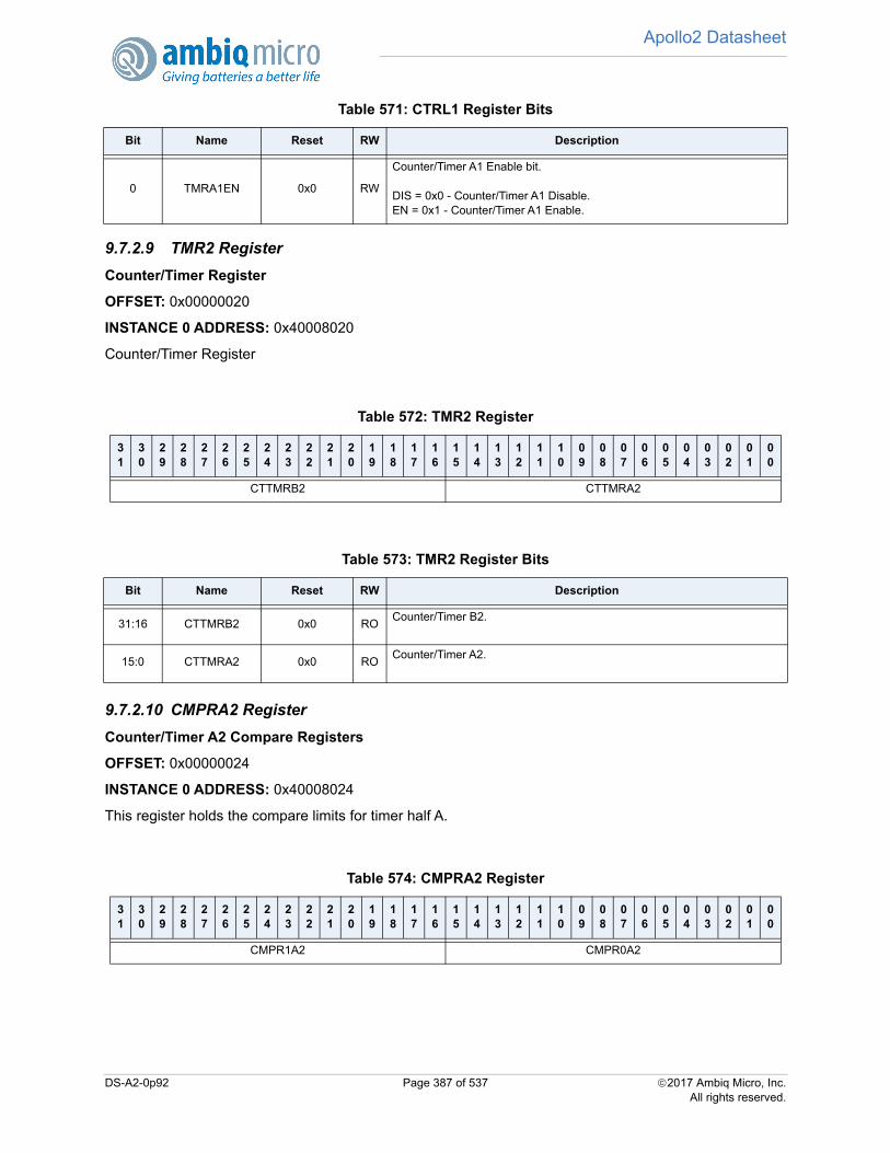
Apollo2 Datasheet
9.7.2.9 TMR2 Register
Counter/Timer Register
OFFSET: 0x00000020
INSTANCE 0 ADDRESS: 0x40008020
Counter/Timer Register
9.7.2.10 CMPRA2 Register
Counter/Timer A2 Compare Registers
OFFSET: 0x00000024
INSTANCE 0 ADDRESS: 0x40008024
This register holds the compare limits for timer half A.
0 TMRA1EN 0x0 RW
Counter/Timer A1 Enable bit.
DIS = 0x0 - Counter/Timer A1 Disable.EN = 0x1 - Counter/Timer A1 Enable.
Table 572: TMR2 Register
31
30
29
28
27
26
25
24
23
22
21
20
19
18
17
16
15
14
13
12
11
10
09
08
07
06
05
04
03
02
01
00
CTTMRB2 CTTMRA2
Table 573: TMR2 Register Bits
Bit Name Reset RW Description
31:16 CTTMRB2 0x0 ROCounter/Timer B2.
15:0 CTTMRA2 0x0 ROCounter/Timer A2.
Table 574: CMPRA2 Register
31
30
29
28
27
26
25
24
23
22
21
20
19
18
17
16
15
14
13
12
11
10
09
08
07
06
05
04
03
02
01
00
CMPR1A2 CMPR0A2
Table 571: CTRL1 Register Bits
Bit Name Reset RW Description
DS-A2-0p92 Page 387 of 537 2017 Ambiq Micro, Inc.All rights reserved.

Apollo2 Datasheet
9.7.2.11 CMPRB2 Register
Counter/Timer B2 Compare Registers
OFFSET: 0x00000028
INSTANCE 0 ADDRESS: 0x40008028
This register holds the compare limits for timer half B.
9.7.2.12 CTRL2 Register
Counter/Timer Control
OFFSET: 0x0000002C
INSTANCE 0 ADDRESS: 0x4000802C
This register holds the control bit fields for both halves of timer 2.
Table 575: CMPRA2 Register Bits
Bit Name Reset RW Description
31:16 CMPR1A2 0x0 RWCounter/Timer A2 Compare Register 1.
15:0 CMPR0A2 0x0 RWCounter/Timer A2 Compare Register 0.
Table 576: CMPRB2 Register
31
30
29
28
27
26
25
24
23
22
21
20
19
18
17
16
15
14
13
12
11
10
09
08
07
06
05
04
03
02
01
00
CMPR1B2 CMPR0B2
Table 577: CMPRB2 Register Bits
Bit Name Reset RW Description
31:16 CMPR1B2 0x0 RWCounter/Timer B2 Compare Register 1.
15:0 CMPR0B2 0x0 RWCounter/Timer B2 Compare Register 0.
DS-A2-0p92 Page 388 of 537 2017 Ambiq Micro, Inc.All rights reserved.
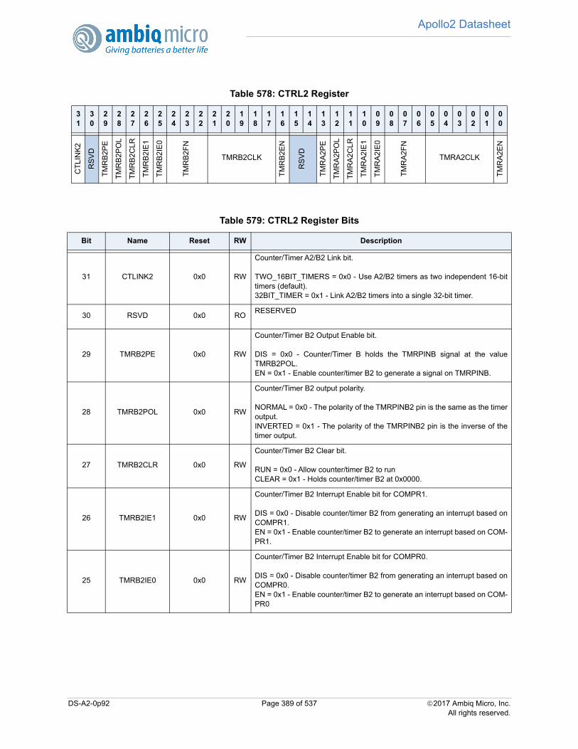
Apollo2 Datasheet
Table 578: CTRL2 Register
31
30
29
28
27
26
25
24
23
22
21
20
19
18
17
16
15
14
13
12
11
10
09
08
07
06
05
04
03
02
01
00
CT
LIN
K2
RS
VD
TM
RB
2PE
TM
RB
2PO
L
TM
RB
2CLR
TM
RB
2IE
1
TM
RB
2IE
0
TM
RB
2FN
TMRB2CLK
TM
RB
2EN
RS
VD
TM
RA
2PE
TM
RA
2PO
L
TM
RA
2CLR
TM
RA
2IE
1
TM
RA
2IE
0
TM
RA
2FN
TMRA2CLK
TM
RA
2EN
Table 579: CTRL2 Register Bits
Bit Name Reset RW Description
31 CTLINK2 0x0 RW
Counter/Timer A2/B2 Link bit.
TWO_16BIT_TIMERS = 0x0 - Use A2/B2 timers as two independent 16-bittimers (default).32BIT_TIMER = 0x1 - Link A2/B2 timers into a single 32-bit timer.
30 RSVD 0x0 RORESERVED
29 TMRB2PE 0x0 RW
Counter/Timer B2 Output Enable bit.
DIS = 0x0 - Counter/Timer B holds the TMRPINB signal at the valueTMRB2POL.EN = 0x1 - Enable counter/timer B2 to generate a signal on TMRPINB.
28 TMRB2POL 0x0 RW
Counter/Timer B2 output polarity.
NORMAL = 0x0 - The polarity of the TMRPINB2 pin is the same as the timeroutput.INVERTED = 0x1 - The polarity of the TMRPINB2 pin is the inverse of thetimer output.
27 TMRB2CLR 0x0 RW
Counter/Timer B2 Clear bit.
RUN = 0x0 - Allow counter/timer B2 to runCLEAR = 0x1 - Holds counter/timer B2 at 0x0000.
26 TMRB2IE1 0x0 RW
Counter/Timer B2 Interrupt Enable bit for COMPR1.
DIS = 0x0 - Disable counter/timer B2 from generating an interrupt based onCOMPR1.EN = 0x1 - Enable counter/timer B2 to generate an interrupt based on COM-PR1.
25 TMRB2IE0 0x0 RW
Counter/Timer B2 Interrupt Enable bit for COMPR0.
DIS = 0x0 - Disable counter/timer B2 from generating an interrupt based onCOMPR0.EN = 0x1 - Enable counter/timer B2 to generate an interrupt based on COM-PR0
DS-A2-0p92 Page 389 of 537 2017 Ambiq Micro, Inc.All rights reserved.
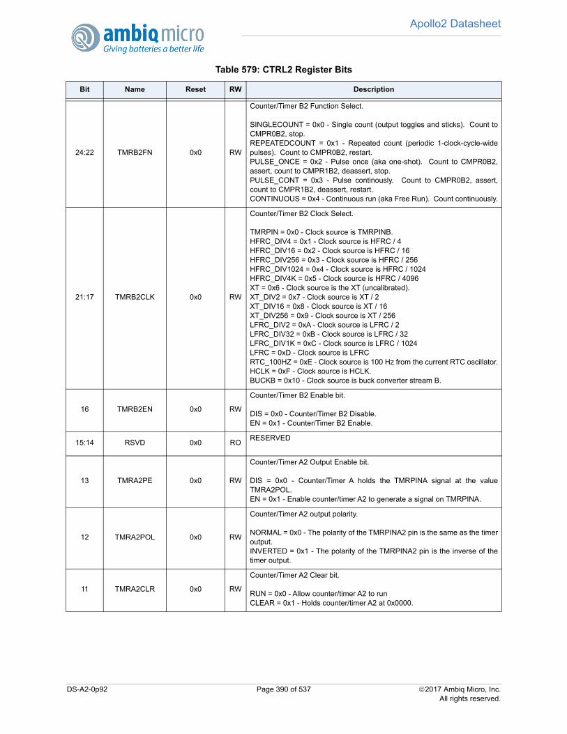
Apollo2 Datasheet
24:22 TMRB2FN 0x0 RW
Counter/Timer B2 Function Select.
SINGLECOUNT = 0x0 - Single count (output toggles and sticks). Count toCMPR0B2, stop.REPEATEDCOUNT = 0x1 - Repeated count (periodic 1-clock-cycle-widepulses). Count to CMPR0B2, restart.PULSE_ONCE = 0x2 - Pulse once (aka one-shot). Count to CMPR0B2,assert, count to CMPR1B2, deassert, stop.PULSE_CONT = 0x3 - Pulse continously. Count to CMPR0B2, assert,count to CMPR1B2, deassert, restart.CONTINUOUS = 0x4 - Continuous run (aka Free Run). Count continuously.
21:17 TMRB2CLK 0x0 RW
Counter/Timer B2 Clock Select.
TMRPIN = 0x0 - Clock source is TMRPINB.HFRC_DIV4 = 0x1 - Clock source is HFRC / 4HFRC_DIV16 = 0x2 - Clock source is HFRC / 16HFRC_DIV256 = 0x3 - Clock source is HFRC / 256HFRC_DIV1024 = 0x4 - Clock source is HFRC / 1024HFRC_DIV4K = 0x5 - Clock source is HFRC / 4096XT = 0x6 - Clock source is the XT (uncalibrated).XT_DIV2 = 0x7 - Clock source is XT / 2XT_DIV16 = 0x8 - Clock source is XT / 16XT_DIV256 = 0x9 - Clock source is XT / 256LFRC_DIV2 = 0xA - Clock source is LFRC / 2LFRC_DIV32 = 0xB - Clock source is LFRC / 32LFRC_DIV1K = 0xC - Clock source is LFRC / 1024LFRC = 0xD - Clock source is LFRCRTC_100HZ = 0xE - Clock source is 100 Hz from the current RTC oscillator.HCLK = 0xF - Clock source is HCLK.BUCKB = 0x10 - Clock source is buck converter stream B.
16 TMRB2EN 0x0 RW
Counter/Timer B2 Enable bit.
DIS = 0x0 - Counter/Timer B2 Disable.EN = 0x1 - Counter/Timer B2 Enable.
15:14 RSVD 0x0 RORESERVED
13 TMRA2PE 0x0 RW
Counter/Timer A2 Output Enable bit.
DIS = 0x0 - Counter/Timer A holds the TMRPINA signal at the valueTMRA2POL.EN = 0x1 - Enable counter/timer A2 to generate a signal on TMRPINA.
12 TMRA2POL 0x0 RW
Counter/Timer A2 output polarity.
NORMAL = 0x0 - The polarity of the TMRPINA2 pin is the same as the timeroutput.INVERTED = 0x1 - The polarity of the TMRPINA2 pin is the inverse of thetimer output.
11 TMRA2CLR 0x0 RW
Counter/Timer A2 Clear bit.
RUN = 0x0 - Allow counter/timer A2 to runCLEAR = 0x1 - Holds counter/timer A2 at 0x0000.
Table 579: CTRL2 Register Bits
Bit Name Reset RW Description
DS-A2-0p92 Page 390 of 537 2017 Ambiq Micro, Inc.All rights reserved.

Apollo2 Datasheet
9.7.2.13 TMR3 Register
Counter/Timer Register
OFFSET: 0x00000030
INSTANCE 0 ADDRESS: 0x40008030
Counter/Timer Register
10 TMRA2IE1 0x0 RW
Counter/Timer A2 Interrupt Enable bit based on COMPR1.
DIS = 0x0 - Disable counter/timer A2 from generating an interrupt based onCOMPR1.EN = 0x1 - Enable counter/timer A2 to generate an interrupt based on COM-PR1.
9 TMRA2IE0 0x0 RW
Counter/Timer A2 Interrupt Enable bit based on COMPR0.
DIS = 0x0 - Disable counter/timer A2 from generating an interrupt based onCOMPR0.EN = 0x1 - Enable counter/timer A2 to generate an interrupt based on COM-PR0.
8:6 TMRA2FN 0x0 RW
Counter/Timer A2 Function Select.
SINGLECOUNT = 0x0 - Single count (output toggles and sticks). Count toCMPR0A2, stop.REPEATEDCOUNT = 0x1 - Repeated count (periodic 1-clock-cycle-widepulses). Count to CMPR0A2, restart.PULSE_ONCE = 0x2 - Pulse once (aka one-shot). Count to CMPR0A2,assert, count to CMPR1A2, deassert, stop.PULSE_CONT = 0x3 - Pulse continously. Count to CMPR0A2, assert,count to CMPR1A2, deassert, restart.CONTINUOUS = 0x4 - Continuous run (aka Free Run). Count continuously.
5:1 TMRA2CLK 0x0 RW
Counter/Timer A2 Clock Select.
TMRPIN = 0x0 - Clock source is TMRPINA.HFRC_DIV4 = 0x1 - Clock source is HFRC / 4HFRC_DIV16 = 0x2 - Clock source is HFRC / 16HFRC_DIV256 = 0x3 - Clock source is HFRC / 256HFRC_DIV1024 = 0x4 - Clock source is HFRC / 1024HFRC_DIV4K = 0x5 - Clock source is HFRC / 4096XT = 0x6 - Clock source is the XT (uncalibrated).XT_DIV2 = 0x7 - Clock source is XT / 2XT_DIV16 = 0x8 - Clock source is XT / 16XT_DIV256 = 0x9 - Clock source is XT / 256LFRC_DIV2 = 0xA - Clock source is LFRC / 2LFRC_DIV32 = 0xB - Clock source is LFRC / 32LFRC_DIV1K = 0xC - Clock source is LFRC / 1024LFRC = 0xD - Clock source is LFRCRTC_100HZ = 0xE - Clock source is 100 Hz from the current RTC oscillator.HCLK = 0xF - Clock source is HCLK.BUCKA = 0x10 - Clock source is buck converter stream A.
0 TMRA2EN 0x0 RW
Counter/Timer A2 Enable bit.
DIS = 0x0 - Counter/Timer A2 Disable.EN = 0x1 - Counter/Timer A2 Enable.
Table 579: CTRL2 Register Bits
Bit Name Reset RW Description
DS-A2-0p92 Page 391 of 537 2017 Ambiq Micro, Inc.All rights reserved.
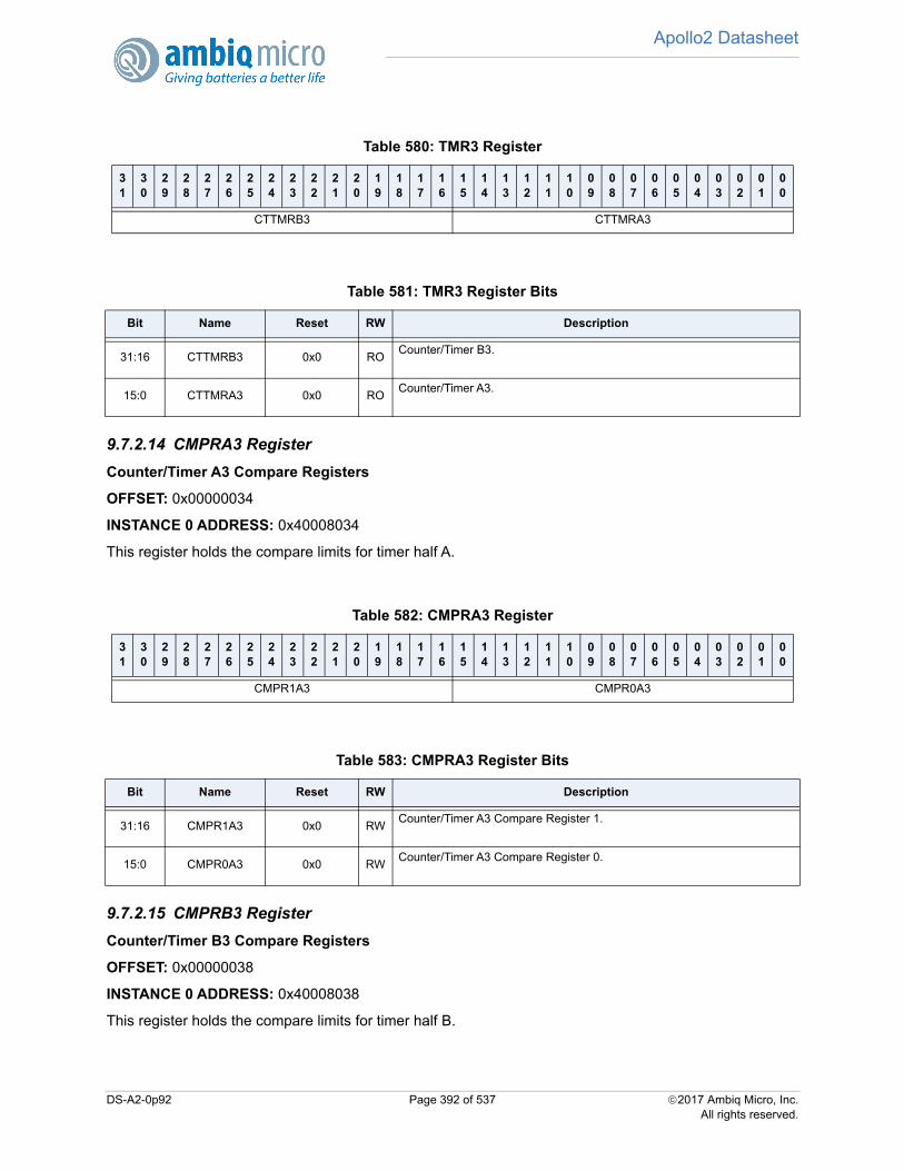
Apollo2 Datasheet
9.7.2.14 CMPRA3 Register
Counter/Timer A3 Compare Registers
OFFSET: 0x00000034
INSTANCE 0 ADDRESS: 0x40008034
This register holds the compare limits for timer half A.
9.7.2.15 CMPRB3 Register
Counter/Timer B3 Compare Registers
OFFSET: 0x00000038
INSTANCE 0 ADDRESS: 0x40008038
This register holds the compare limits for timer half B.
Table 580: TMR3 Register
31
30
29
28
27
26
25
24
23
22
21
20
19
18
17
16
15
14
13
12
11
10
09
08
07
06
05
04
03
02
01
00
CTTMRB3 CTTMRA3
Table 581: TMR3 Register Bits
Bit Name Reset RW Description
31:16 CTTMRB3 0x0 ROCounter/Timer B3.
15:0 CTTMRA3 0x0 ROCounter/Timer A3.
Table 582: CMPRA3 Register
31
30
29
28
27
26
25
24
23
22
21
20
19
18
17
16
15
14
13
12
11
10
09
08
07
06
05
04
03
02
01
00
CMPR1A3 CMPR0A3
Table 583: CMPRA3 Register Bits
Bit Name Reset RW Description
31:16 CMPR1A3 0x0 RWCounter/Timer A3 Compare Register 1.
15:0 CMPR0A3 0x0 RWCounter/Timer A3 Compare Register 0.
DS-A2-0p92 Page 392 of 537 2017 Ambiq Micro, Inc.All rights reserved.
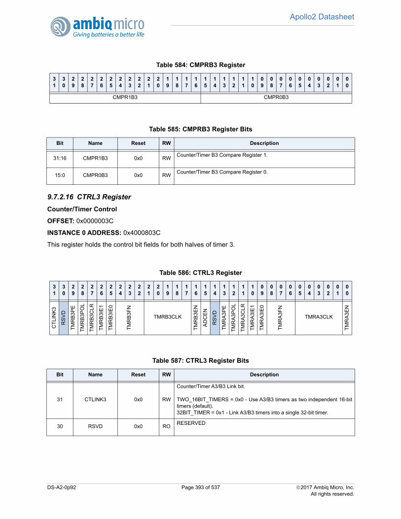
Apollo2 Datasheet
9.7.2.16 CTRL3 Register
Counter/Timer Control
OFFSET: 0x0000003C
INSTANCE 0 ADDRESS: 0x4000803C
This register holds the control bit fields for both halves of timer 3.
Table 584: CMPRB3 Register
31
30
29
28
27
26
25
24
23
22
21
20
19
18
17
16
15
14
13
12
11
10
09
08
07
06
05
04
03
02
01
00
CMPR1B3 CMPR0B3
Table 585: CMPRB3 Register Bits
Bit Name Reset RW Description
31:16 CMPR1B3 0x0 RWCounter/Timer B3 Compare Register 1.
15:0 CMPR0B3 0x0 RWCounter/Timer B3 Compare Register 0.
Table 586: CTRL3 Register
31
30
29
28
27
26
25
24
23
22
21
20
19
18
17
16
15
14
13
12
11
10
09
08
07
06
05
04
03
02
01
00
CT
LIN
K3
RS
VD
TM
RB
3P
E
TM
RB
3PO
L
TM
RB
3CLR
TM
RB
3IE
1
TM
RB
3IE
0
TM
RB
3FN
TMRB3CLK
TM
RB
3EN
AD
CE
N
RS
VD
TM
RA
3P
E
TM
RA
3PO
L
TM
RA
3CLR
TM
RA
3IE
1
TM
RA
3IE
0
TM
RA
3FN
TMRA3CLK
TM
RA
3EN
Table 587: CTRL3 Register Bits
Bit Name Reset RW Description
31 CTLINK3 0x0 RW
Counter/Timer A3/B3 Link bit.
TWO_16BIT_TIMERS = 0x0 - Use A3/B3 timers as two independent 16-bittimers (default).32BIT_TIMER = 0x1 - Link A3/B3 timers into a single 32-bit timer.
30 RSVD 0x0 RORESERVED
DS-A2-0p92 Page 393 of 537 2017 Ambiq Micro, Inc.All rights reserved.

Apollo2 Datasheet
29 TMRB3PE 0x0 RW
Counter/Timer B3 Output Enable bit.
DIS = 0x0 - Counter/Timer B holds the TMRPINB signal at the valueTMRB3POL.EN = 0x1 - Enable counter/timer B3 to generate a signal on TMRPINB.
28 TMRB3POL 0x0 RW
Counter/Timer B3 output polarity.
NORMAL = 0x0 - The polarity of the TMRPINB3 pin is the same as the timeroutput.INVERTED = 0x1 - The polarity of the TMRPINB3 pin is the inverse of thetimer output.
27 TMRB3CLR 0x0 RW
Counter/Timer B3 Clear bit.
RUN = 0x0 - Allow counter/timer B3 to runCLEAR = 0x1 - Holds counter/timer B3 at 0x0000.
26 TMRB3IE1 0x0 RW
Counter/Timer B3 Interrupt Enable bit for COMPR1.
DIS = 0x0 - Disable counter/timer B3 from generating an interrupt based onCOMPR1.EN = 0x1 - Enable counter/timer B3 to generate an interrupt based on COM-PR1.
25 TMRB3IE0 0x0 RW
Counter/Timer B3 Interrupt Enable bit for COMPR0.
DIS = 0x0 - Disable counter/timer B3 from generating an interrupt based onCOMPR0.EN = 0x1 - Enable counter/timer B3 to generate an interrupt based on COM-PR0
24:22 TMRB3FN 0x0 RW
Counter/Timer B3 Function Select.
SINGLECOUNT = 0x0 - Single count (output toggles and sticks). Count toCMPR0B3, stop.REPEATEDCOUNT = 0x1 - Repeated count (periodic 1-clock-cycle-widepulses). Count to CMPR0B3, restart.PULSE_ONCE = 0x2 - Pulse once (aka one-shot). Count to CMPR0B3,assert, count to CMPR1B3, deassert, stop.PULSE_CONT = 0x3 - Pulse continously. Count to CMPR0B3, assert,count to CMPR1B3, deassert, restart.CONTINUOUS = 0x4 - Continuous run (aka Free Run). Count continuously.
21:17 TMRB3CLK 0x0 RW
Counter/Timer B3 Clock Select.
TMRPIN = 0x0 - Clock source is TMRPINB.HFRC_DIV4 = 0x1 - Clock source is HFRC / 4HFRC_DIV16 = 0x2 - Clock source is HFRC / 16HFRC_DIV256 = 0x3 - Clock source is HFRC / 256HFRC_DIV1024 = 0x4 - Clock source is HFRC / 1024HFRC_DIV4K = 0x5 - Clock source is HFRC / 4096XT = 0x6 - Clock source is the XT (uncalibrated).XT_DIV2 = 0x7 - Clock source is XT / 2XT_DIV16 = 0x8 - Clock source is XT / 16XT_DIV256 = 0x9 - Clock source is XT / 256LFRC_DIV2 = 0xA - Clock source is LFRC / 2LFRC_DIV32 = 0xB - Clock source is LFRC / 32LFRC_DIV1K = 0xC - Clock source is LFRC / 1024LFRC = 0xD - Clock source is LFRCRTC_100HZ = 0xE - Clock source is 100 Hz from the current RTC oscillator.HCLK = 0xF - Clock source is HCLK.BUCKB = 0x10 - Clock source is buck converter stream B.
Table 587: CTRL3 Register Bits
Bit Name Reset RW Description
DS-A2-0p92 Page 394 of 537 2017 Ambiq Micro, Inc.All rights reserved.
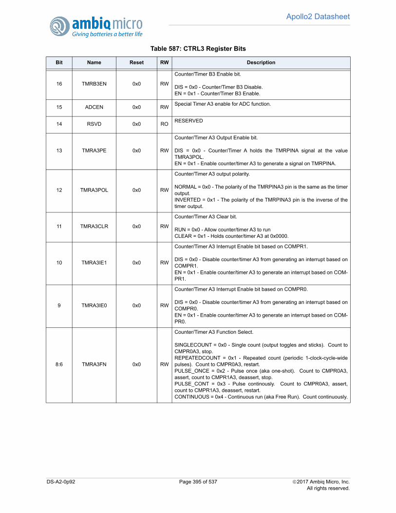
Apollo2 Datasheet
16 TMRB3EN 0x0 RW
Counter/Timer B3 Enable bit.
DIS = 0x0 - Counter/Timer B3 Disable.EN = 0x1 - Counter/Timer B3 Enable.
15 ADCEN 0x0 RWSpecial Timer A3 enable for ADC function.
14 RSVD 0x0 RORESERVED
13 TMRA3PE 0x0 RW
Counter/Timer A3 Output Enable bit.
DIS = 0x0 - Counter/Timer A holds the TMRPINA signal at the valueTMRA3POL.EN = 0x1 - Enable counter/timer A3 to generate a signal on TMRPINA.
12 TMRA3POL 0x0 RW
Counter/Timer A3 output polarity.
NORMAL = 0x0 - The polarity of the TMRPINA3 pin is the same as the timeroutput.INVERTED = 0x1 - The polarity of the TMRPINA3 pin is the inverse of thetimer output.
11 TMRA3CLR 0x0 RW
Counter/Timer A3 Clear bit.
RUN = 0x0 - Allow counter/timer A3 to runCLEAR = 0x1 - Holds counter/timer A3 at 0x0000.
10 TMRA3IE1 0x0 RW
Counter/Timer A3 Interrupt Enable bit based on COMPR1.
DIS = 0x0 - Disable counter/timer A3 from generating an interrupt based onCOMPR1.EN = 0x1 - Enable counter/timer A3 to generate an interrupt based on COM-PR1.
9 TMRA3IE0 0x0 RW
Counter/Timer A3 Interrupt Enable bit based on COMPR0.
DIS = 0x0 - Disable counter/timer A3 from generating an interrupt based onCOMPR0.EN = 0x1 - Enable counter/timer A3 to generate an interrupt based on COM-PR0.
8:6 TMRA3FN 0x0 RW
Counter/Timer A3 Function Select.
SINGLECOUNT = 0x0 - Single count (output toggles and sticks). Count toCMPR0A3, stop.REPEATEDCOUNT = 0x1 - Repeated count (periodic 1-clock-cycle-widepulses). Count to CMPR0A3, restart.PULSE_ONCE = 0x2 - Pulse once (aka one-shot). Count to CMPR0A3,assert, count to CMPR1A3, deassert, stop.PULSE_CONT = 0x3 - Pulse continously. Count to CMPR0A3, assert,count to CMPR1A3, deassert, restart.CONTINUOUS = 0x4 - Continuous run (aka Free Run). Count continuously.
Table 587: CTRL3 Register Bits
Bit Name Reset RW Description
DS-A2-0p92 Page 395 of 537 2017 Ambiq Micro, Inc.All rights reserved.

Apollo2 Datasheet
9.7.2.17 INTEN Register
Counter/Timer Interrupts: Enable
OFFSET: 0x00000200
INSTANCE 0 ADDRESS: 0x40008200
Set bits in this register to allow this module to generate the corresponding interrupt.
5:1 TMRA3CLK 0x0 RW
Counter/Timer A3 Clock Select.
TMRPIN = 0x0 - Clock source is TMRPINA.HFRC_DIV4 = 0x1 - Clock source is HFRC / 4HFRC_DIV16 = 0x2 - Clock source is HFRC / 16HFRC_DIV256 = 0x3 - Clock source is HFRC / 256HFRC_DIV1024 = 0x4 - Clock source is HFRC / 1024HFRC_DIV4K = 0x5 - Clock source is HFRC / 4096XT = 0x6 - Clock source is the XT (uncalibrated).XT_DIV2 = 0x7 - Clock source is XT / 2XT_DIV16 = 0x8 - Clock source is XT / 16XT_DIV256 = 0x9 - Clock source is XT / 256LFRC_DIV2 = 0xA - Clock source is LFRC / 2LFRC_DIV32 = 0xB - Clock source is LFRC / 32LFRC_DIV1K = 0xC - Clock source is LFRC / 1024LFRC = 0xD - Clock source is LFRCRTC_100HZ = 0xE - Clock source is 100 Hz from the current RTC oscillator.HCLK = 0xF - Clock source is HCLK.BUCKA = 0x10 - Clock source is buck converter stream A.
0 TMRA3EN 0x0 RW
Counter/Timer A3 Enable bit.
DIS = 0x0 - Counter/Timer A3 Disable.EN = 0x1 - Counter/Timer A3 Enable.
Table 588: INTEN Register
31
30
29
28
27
26
25
24
23
22
21
20
19
18
17
16
15
14
13
12
11
10
09
08
07
06
05
04
03
02
01
00
RSVD
CT
MR
B3C
1IN
T
CT
MR
A3C
1IN
T
CT
MR
B2C
1IN
T
CT
MR
A2C
1IN
T
CT
MR
B1C
1IN
T
CT
MR
A1C
1IN
T
CT
MR
B0C
1IN
T
CT
MR
A0C
1IN
T
CT
MR
B3C
0IN
T
CT
MR
A3C
0IN
T
CT
MR
B2C
0IN
T
CT
MR
A2C
0IN
T
CT
MR
B1C
0IN
T
CT
MR
A1C
0IN
T
CT
MR
B0C
0IN
T
CT
MR
A0C
0IN
T
Table 589: INTEN Register Bits
Bit Name Reset RW Description
31:16 RSVD 0x0 RORESERVED
15 CTMRB3C1INT 0x0 RWCounter/Timer B3 interrupt based on COMPR1.
Table 587: CTRL3 Register Bits
Bit Name Reset RW Description
DS-A2-0p92 Page 396 of 537 2017 Ambiq Micro, Inc.All rights reserved.
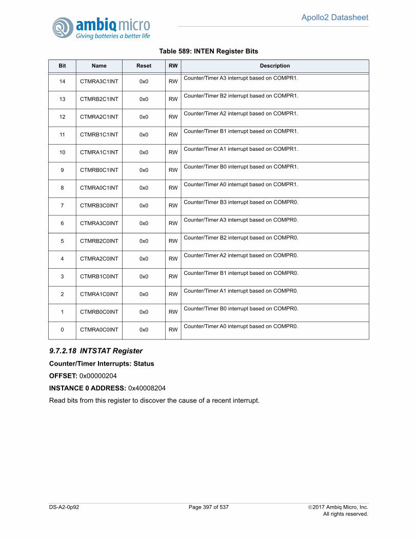
Apollo2 Datasheet
9.7.2.18 INTSTAT Register
Counter/Timer Interrupts: Status
OFFSET: 0x00000204
INSTANCE 0 ADDRESS: 0x40008204
Read bits from this register to discover the cause of a recent interrupt.
14 CTMRA3C1INT 0x0 RWCounter/Timer A3 interrupt based on COMPR1.
13 CTMRB2C1INT 0x0 RWCounter/Timer B2 interrupt based on COMPR1.
12 CTMRA2C1INT 0x0 RWCounter/Timer A2 interrupt based on COMPR1.
11 CTMRB1C1INT 0x0 RWCounter/Timer B1 interrupt based on COMPR1.
10 CTMRA1C1INT 0x0 RWCounter/Timer A1 interrupt based on COMPR1.
9 CTMRB0C1INT 0x0 RWCounter/Timer B0 interrupt based on COMPR1.
8 CTMRA0C1INT 0x0 RWCounter/Timer A0 interrupt based on COMPR1.
7 CTMRB3C0INT 0x0 RWCounter/Timer B3 interrupt based on COMPR0.
6 CTMRA3C0INT 0x0 RWCounter/Timer A3 interrupt based on COMPR0.
5 CTMRB2C0INT 0x0 RWCounter/Timer B2 interrupt based on COMPR0.
4 CTMRA2C0INT 0x0 RWCounter/Timer A2 interrupt based on COMPR0.
3 CTMRB1C0INT 0x0 RWCounter/Timer B1 interrupt based on COMPR0.
2 CTMRA1C0INT 0x0 RWCounter/Timer A1 interrupt based on COMPR0.
1 CTMRB0C0INT 0x0 RWCounter/Timer B0 interrupt based on COMPR0.
0 CTMRA0C0INT 0x0 RWCounter/Timer A0 interrupt based on COMPR0.
Table 589: INTEN Register Bits
Bit Name Reset RW Description
DS-A2-0p92 Page 397 of 537 2017 Ambiq Micro, Inc.All rights reserved.
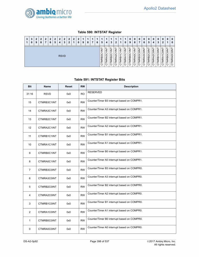
Apollo2 Datasheet
Table 590: INTSTAT Register
31
30
29
28
27
26
25
24
23
22
21
20
19
18
17
16
15
14
13
12
11
10
09
08
07
06
05
04
03
02
01
00
RSVD
CT
MR
B3
C1I
NT
CT
MR
A3
C1I
NT
CT
MR
B2
C1I
NT
CT
MR
A2
C1I
NT
CT
MR
B1
C1I
NT
CT
MR
A1
C1I
NT
CT
MR
B0
C1I
NT
CT
MR
A0
C1I
NT
CT
MR
B3
C0I
NT
CT
MR
A3
C0I
NT
CT
MR
B2
C0I
NT
CT
MR
A2
C0I
NT
CT
MR
B1
C0I
NT
CT
MR
A1
C0I
NT
CT
MR
B0
C0I
NT
CT
MR
A0
C0I
NT
Table 591: INTSTAT Register Bits
Bit Name Reset RW Description
31:16 RSVD 0x0 RORESERVED
15 CTMRB3C1INT 0x0 RWCounter/Timer B3 interrupt based on COMPR1.
14 CTMRA3C1INT 0x0 RWCounter/Timer A3 interrupt based on COMPR1.
13 CTMRB2C1INT 0x0 RWCounter/Timer B2 interrupt based on COMPR1.
12 CTMRA2C1INT 0x0 RWCounter/Timer A2 interrupt based on COMPR1.
11 CTMRB1C1INT 0x0 RWCounter/Timer B1 interrupt based on COMPR1.
10 CTMRA1C1INT 0x0 RWCounter/Timer A1 interrupt based on COMPR1.
9 CTMRB0C1INT 0x0 RWCounter/Timer B0 interrupt based on COMPR1.
8 CTMRA0C1INT 0x0 RWCounter/Timer A0 interrupt based on COMPR1.
7 CTMRB3C0INT 0x0 RWCounter/Timer B3 interrupt based on COMPR0.
6 CTMRA3C0INT 0x0 RWCounter/Timer A3 interrupt based on COMPR0.
5 CTMRB2C0INT 0x0 RWCounter/Timer B2 interrupt based on COMPR0.
4 CTMRA2C0INT 0x0 RWCounter/Timer A2 interrupt based on COMPR0.
3 CTMRB1C0INT 0x0 RWCounter/Timer B1 interrupt based on COMPR0.
2 CTMRA1C0INT 0x0 RWCounter/Timer A1 interrupt based on COMPR0.
1 CTMRB0C0INT 0x0 RWCounter/Timer B0 interrupt based on COMPR0.
0 CTMRA0C0INT 0x0 RWCounter/Timer A0 interrupt based on COMPR0.
DS-A2-0p92 Page 398 of 537 2017 Ambiq Micro, Inc.All rights reserved.
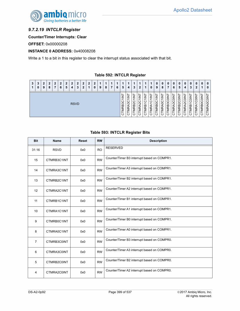
Apollo2 Datasheet
9.7.2.19 INTCLR Register
Counter/Timer Interrupts: Clear
OFFSET: 0x00000208
INSTANCE 0 ADDRESS: 0x40008208
Write a 1 to a bit in this register to clear the interrupt status associated with that bit.
Table 592: INTCLR Register
31
30
29
28
27
26
25
24
23
22
21
20
19
18
17
16
15
14
13
12
11
10
09
08
07
06
05
04
03
02
01
00
RSVD
CT
MR
B3C
1IN
T
CT
MR
A3C
1IN
T
CT
MR
B2C
1IN
T
CT
MR
A2C
1IN
T
CT
MR
B1C
1IN
T
CT
MR
A1C
1IN
T
CT
MR
B0C
1IN
T
CT
MR
A0C
1IN
T
CT
MR
B3C
0IN
T
CT
MR
A3C
0IN
T
CT
MR
B2C
0IN
T
CT
MR
A2C
0IN
T
CT
MR
B1C
0IN
T
CT
MR
A1C
0IN
T
CT
MR
B0C
0IN
T
CT
MR
A0C
0IN
T
Table 593: INTCLR Register Bits
Bit Name Reset RW Description
31:16 RSVD 0x0 RORESERVED
15 CTMRB3C1INT 0x0 RWCounter/Timer B3 interrupt based on COMPR1.
14 CTMRA3C1INT 0x0 RWCounter/Timer A3 interrupt based on COMPR1.
13 CTMRB2C1INT 0x0 RWCounter/Timer B2 interrupt based on COMPR1.
12 CTMRA2C1INT 0x0 RWCounter/Timer A2 interrupt based on COMPR1.
11 CTMRB1C1INT 0x0 RWCounter/Timer B1 interrupt based on COMPR1.
10 CTMRA1C1INT 0x0 RWCounter/Timer A1 interrupt based on COMPR1.
9 CTMRB0C1INT 0x0 RWCounter/Timer B0 interrupt based on COMPR1.
8 CTMRA0C1INT 0x0 RWCounter/Timer A0 interrupt based on COMPR1.
7 CTMRB3C0INT 0x0 RWCounter/Timer B3 interrupt based on COMPR0.
6 CTMRA3C0INT 0x0 RWCounter/Timer A3 interrupt based on COMPR0.
5 CTMRB2C0INT 0x0 RWCounter/Timer B2 interrupt based on COMPR0.
4 CTMRA2C0INT 0x0 RWCounter/Timer A2 interrupt based on COMPR0.
DS-A2-0p92 Page 399 of 537 2017 Ambiq Micro, Inc.All rights reserved.
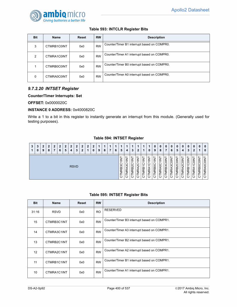
Apollo2 Datasheet
9.7.2.20 INTSET Register
Counter/Timer Interrupts: Set
OFFSET: 0x0000020C
INSTANCE 0 ADDRESS: 0x4000820C
Write a 1 to a bit in this register to instantly generate an interrupt from this module. (Generally used fortesting purposes).
3 CTMRB1C0INT 0x0 RWCounter/Timer B1 interrupt based on COMPR0.
2 CTMRA1C0INT 0x0 RWCounter/Timer A1 interrupt based on COMPR0.
1 CTMRB0C0INT 0x0 RWCounter/Timer B0 interrupt based on COMPR0.
0 CTMRA0C0INT 0x0 RWCounter/Timer A0 interrupt based on COMPR0.
Table 594: INTSET Register
31
30
29
28
27
26
25
24
23
22
21
20
19
18
17
16
15
14
13
12
11
10
09
08
07
06
05
04
03
02
01
00
RSVD
CT
MR
B3C
1IN
T
CT
MR
A3C
1IN
T
CT
MR
B2C
1IN
T
CT
MR
A2C
1IN
T
CT
MR
B1C
1IN
T
CT
MR
A1C
1IN
T
CT
MR
B0C
1IN
T
CT
MR
A0C
1IN
T
CT
MR
B3C
0IN
T
CT
MR
A3C
0IN
T
CT
MR
B2C
0IN
T
CT
MR
A2C
0IN
T
CT
MR
B1C
0IN
T
CT
MR
A1C
0IN
T
CT
MR
B0C
0IN
T
CT
MR
A0C
0IN
T
Table 595: INTSET Register Bits
Bit Name Reset RW Description
31:16 RSVD 0x0 RORESERVED
15 CTMRB3C1INT 0x0 RWCounter/Timer B3 interrupt based on COMPR1.
14 CTMRA3C1INT 0x0 RWCounter/Timer A3 interrupt based on COMPR1.
13 CTMRB2C1INT 0x0 RWCounter/Timer B2 interrupt based on COMPR1.
12 CTMRA2C1INT 0x0 RWCounter/Timer A2 interrupt based on COMPR1.
11 CTMRB1C1INT 0x0 RWCounter/Timer B1 interrupt based on COMPR1.
10 CTMRA1C1INT 0x0 RWCounter/Timer A1 interrupt based on COMPR1.
Table 593: INTCLR Register Bits
Bit Name Reset RW Description
DS-A2-0p92 Page 400 of 537 2017 Ambiq Micro, Inc.All rights reserved.

Apollo2 Datasheet
9 CTMRB0C1INT 0x0 RWCounter/Timer B0 interrupt based on COMPR1.
8 CTMRA0C1INT 0x0 RWCounter/Timer A0 interrupt based on COMPR1.
7 CTMRB3C0INT 0x0 RWCounter/Timer B3 interrupt based on COMPR0.
6 CTMRA3C0INT 0x0 RWCounter/Timer A3 interrupt based on COMPR0.
5 CTMRB2C0INT 0x0 RWCounter/Timer B2 interrupt based on COMPR0.
4 CTMRA2C0INT 0x0 RWCounter/Timer A2 interrupt based on COMPR0.
3 CTMRB1C0INT 0x0 RWCounter/Timer B1 interrupt based on COMPR0.
2 CTMRA1C0INT 0x0 RWCounter/Timer A1 interrupt based on COMPR0.
1 CTMRB0C0INT 0x0 RWCounter/Timer B0 interrupt based on COMPR0.
0 CTMRA0C0INT 0x0 RWCounter/Timer A0 interrupt based on COMPR0.
Table 595: INTSET Register Bits
Bit Name Reset RW Description
DS-A2-0p92 Page 401 of 537 2017 Ambiq Micro, Inc.All rights reserved.

Apollo2 Datasheet
10. System Timer Module
Figure 59. Block Diagram for the System Timer
10.1 Functional OverviewThe Apollo2 MCU System Timer (STIMER), shown above in Figure 59, tracks the global synchronizedcounter. It can be used for RTOS scheduling and real-time system tracking. This timer is provided inaddition to the other timer peripherals to enable software/firmware to have a simple, globally synchronizedtimer source.
The System Timer (STIMER) Module provides real time measurement for all task scheduling, sensorsample rate calibration, and tracking of real time and calendar maintenance. Key features are:
32-bit binary counter used for RTOS scheduling decisions. Eight 32-bit compare and interrupt registers to facilitate light weight scheduling (designs without RTOS). Accurate scheduling of comparator interrupts Only offsets from “NOW” are written to comparator registers. Maintains real time epoch for applications. Overflow interrupt to allow firmware to keep the extended part (more than 32-bits) of real time epoch. Time stamping hardware for multiple sensor streams (4 capture registers). Firmware handling of odd calculations such as Leap Second. It also handles things like surprise/legis-
lated changes to the daylight savings time transition dates. Firmware handling of 1024 versus 1000 scaling of real time conversions. Only reset by POA (system cold reset) so that it retains time across all POI and POR (system warm
reset) events except full power cycles. Contains three 32-bit NVRAM registers that are only reset by POA to maintain real time offset from
epoch.
32-bit system timer
=
CLK
Comp IRQ
32-bit compare value( x 8)
32-bit capture registers( x 4) GPIO
OVF IRQCapture IRQ
DS-A2-0p92 Page 402 of 537 2017 Ambiq Micro, Inc.All rights reserved.
Apollo2 Datasheet
The heart of the STIMER is a single 32-bit counter that keeps track of current time for the applicationrunning on the Apollo2 MCU. This counter is reset at the actual power cycle reset of the MCU. It isgenerally never reset or changed again. Up to eight 32-bit comparator registers can be loaded each ofwhich can generate an interrupt signal to the NVIC. Comparators A through H generate interrupt A throughH while capture registers A through D and the overflow event generate interrupt I, all the way to the NVIC.Thus the scheduler can run these 9 interrupts at different priorities in the NVIC.
The comparator interrupts are each used to schedule a function (task) to run for the application. Thusthese tasks run on interrupt levels at priorities lower than the I/O interrupts.
The overflow interrupt allows firmware to keep track of real time beyond that maintained in the 32-bit timer.
10.2 STIMER RegistersSystem Timer
INSTANCE 0 BASE ADDRESS:0x40008000
The System Timer block contains a 32-bit counter for system timer functions. This counter is the source fortimestamping events when performing capture or compare functions.
DS-A2-0p92 Page 403 of 537 2017 Ambiq Micro, Inc.All rights reserved.
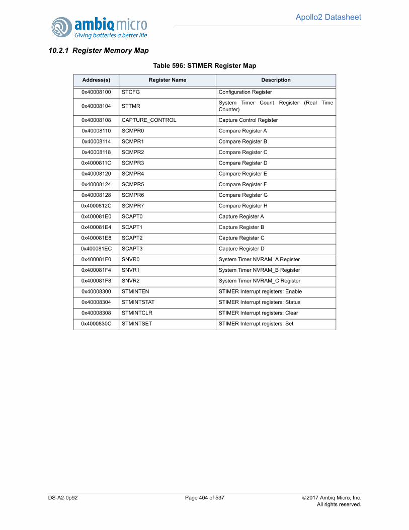
Apollo2 Datasheet
10.2.1 Register Memory Map
Table 596: STIMER Register Map
Address(s) Register Name Description
0x40008100 STCFG Configuration Register
0x40008104 STTMRSystem Timer Count Register (Real TimeCounter)
0x40008108 CAPTURE_CONTROL Capture Control Register
0x40008110 SCMPR0 Compare Register A
0x40008114 SCMPR1 Compare Register B
0x40008118 SCMPR2 Compare Register C
0x4000811C SCMPR3 Compare Register D
0x40008120 SCMPR4 Compare Register E
0x40008124 SCMPR5 Compare Register F
0x40008128 SCMPR6 Compare Register G
0x4000812C SCMPR7 Compare Register H
0x400081E0 SCAPT0 Capture Register A
0x400081E4 SCAPT1 Capture Register B
0x400081E8 SCAPT2 Capture Register C
0x400081EC SCAPT3 Capture Register D
0x400081F0 SNVR0 System Timer NVRAM_A Register
0x400081F4 SNVR1 System Timer NVRAM_B Register
0x400081F8 SNVR2 System Timer NVRAM_C Register
0x40008300 STMINTEN STIMER Interrupt registers: Enable
0x40008304 STMINTSTAT STIMER Interrupt registers: Status
0x40008308 STMINTCLR STIMER Interrupt registers: Clear
0x4000830C STMINTSET STIMER Interrupt registers: Set
DS-A2-0p92 Page 404 of 537 2017 Ambiq Micro, Inc.All rights reserved.
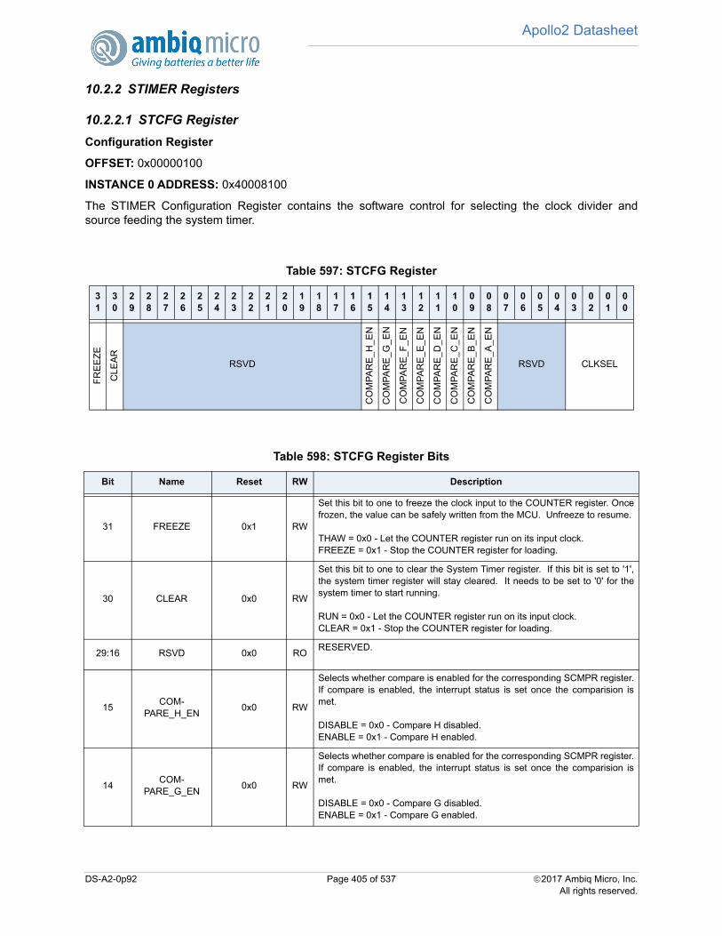
Apollo2 Datasheet
10.2.2 STIMER Registers
10.2.2.1 STCFG Register
Configuration Register
OFFSET: 0x00000100
INSTANCE 0 ADDRESS: 0x40008100
The STIMER Configuration Register contains the software control for selecting the clock divider andsource feeding the system timer.
Table 597: STCFG Register
31
30
29
28
27
26
25
24
23
22
21
20
19
18
17
16
15
14
13
12
11
10
09
08
07
06
05
04
03
02
01
00
FR
EE
ZE
CLE
AR
RSVDC
OM
PA
RE
_H_E
N
CO
MP
AR
E_G
_EN
CO
MP
AR
E_
F_
EN
CO
MP
AR
E_E
_EN
CO
MP
AR
E_D
_EN
CO
MP
AR
E_C
_EN
CO
MP
AR
E_B
_EN
CO
MP
AR
E_A
_EN
RSVD CLKSEL
Table 598: STCFG Register Bits
Bit Name Reset RW Description
31 FREEZE 0x1 RW
Set this bit to one to freeze the clock input to the COUNTER register. Oncefrozen, the value can be safely written from the MCU. Unfreeze to resume.
THAW = 0x0 - Let the COUNTER register run on its input clock.FREEZE = 0x1 - Stop the COUNTER register for loading.
30 CLEAR 0x0 RW
Set this bit to one to clear the System Timer register. If this bit is set to '1',the system timer register will stay cleared. It needs to be set to '0' for thesystem timer to start running.
RUN = 0x0 - Let the COUNTER register run on its input clock.CLEAR = 0x1 - Stop the COUNTER register for loading.
29:16 RSVD 0x0 RORESERVED.
15COM-
PARE_H_EN0x0 RW
Selects whether compare is enabled for the corresponding SCMPR register.If compare is enabled, the interrupt status is set once the comparision ismet.
DISABLE = 0x0 - Compare H disabled.ENABLE = 0x1 - Compare H enabled.
14COM-
PARE_G_EN0x0 RW
Selects whether compare is enabled for the corresponding SCMPR register.If compare is enabled, the interrupt status is set once the comparision ismet.
DISABLE = 0x0 - Compare G disabled.ENABLE = 0x1 - Compare G enabled.
DS-A2-0p92 Page 405 of 537 2017 Ambiq Micro, Inc.All rights reserved.
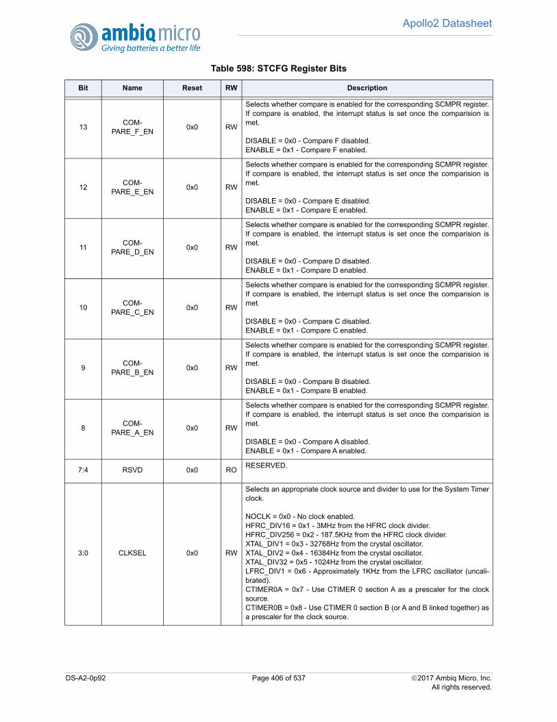
Apollo2 Datasheet
13COM-
PARE_F_EN0x0 RW
Selects whether compare is enabled for the corresponding SCMPR register.If compare is enabled, the interrupt status is set once the comparision ismet.
DISABLE = 0x0 - Compare F disabled.ENABLE = 0x1 - Compare F enabled.
12COM-
PARE_E_EN0x0 RW
Selects whether compare is enabled for the corresponding SCMPR register.If compare is enabled, the interrupt status is set once the comparision ismet.
DISABLE = 0x0 - Compare E disabled.ENABLE = 0x1 - Compare E enabled.
11COM-
PARE_D_EN0x0 RW
Selects whether compare is enabled for the corresponding SCMPR register.If compare is enabled, the interrupt status is set once the comparision ismet.
DISABLE = 0x0 - Compare D disabled.ENABLE = 0x1 - Compare D enabled.
10COM-
PARE_C_EN0x0 RW
Selects whether compare is enabled for the corresponding SCMPR register.If compare is enabled, the interrupt status is set once the comparision ismet.
DISABLE = 0x0 - Compare C disabled.ENABLE = 0x1 - Compare C enabled.
9COM-
PARE_B_EN0x0 RW
Selects whether compare is enabled for the corresponding SCMPR register.If compare is enabled, the interrupt status is set once the comparision ismet.
DISABLE = 0x0 - Compare B disabled.ENABLE = 0x1 - Compare B enabled.
8COM-
PARE_A_EN0x0 RW
Selects whether compare is enabled for the corresponding SCMPR register.If compare is enabled, the interrupt status is set once the comparision ismet.
DISABLE = 0x0 - Compare A disabled.ENABLE = 0x1 - Compare A enabled.
7:4 RSVD 0x0 RORESERVED.
3:0 CLKSEL 0x0 RW
Selects an appropriate clock source and divider to use for the System Timerclock.
NOCLK = 0x0 - No clock enabled.HFRC_DIV16 = 0x1 - 3MHz from the HFRC clock divider.HFRC_DIV256 = 0x2 - 187.5KHz from the HFRC clock divider.XTAL_DIV1 = 0x3 - 32768Hz from the crystal oscillator.XTAL_DIV2 = 0x4 - 16384Hz from the crystal oscillator.XTAL_DIV32 = 0x5 - 1024Hz from the crystal oscillator.LFRC_DIV1 = 0x6 - Approximately 1KHz from the LFRC oscillator (uncali-brated).CTIMER0A = 0x7 - Use CTIMER 0 section A as a prescaler for the clocksource.CTIMER0B = 0x8 - Use CTIMER 0 section B (or A and B linked together) asa prescaler for the clock source.
Table 598: STCFG Register Bits
Bit Name Reset RW Description
DS-A2-0p92 Page 406 of 537 2017 Ambiq Micro, Inc.All rights reserved.

Apollo2 Datasheet
10.2.2.2 STTMR Register
System Timer Count Register (Real Time Counter)
OFFSET: 0x00000104
INSTANCE 0 ADDRESS: 0x40008104
The COUNTER Register contains the running count of time as maintained by incrementing for every risingclock edge of the clock source selected in the configuration register. It is this counter value that captured inthe capture registers and it is this counter value that is compared against the various compare registers.Writing to this register will ultimately set the COUNTER VALUE to the specified value. WARNING there isan asynchronous clock crossing on the read and write path which can add several STIMER clocks ofuncertainty to reading or setting. Use the FREEZE bit in the DEBUG register to safely write to this registerfor diagnostic purposes.
10.2.2.3 CAPTURE_CONTROL Register
Capture Control Register
OFFSET: 0x00000108
INSTANCE 0 ADDRESS: 0x40008108
The STIMER Capture Control Register controls each of the 4 capture registers. It selects their GPIO pinnumber for a trigger source, enables a capture operation and sets the input polarity for the capture. NOTE:8-bit writes can control individual capture registers atomically.
Table 599: STTMR Register
31
30
29
28
27
26
25
24
23
22
21
20
19
18
17
16
15
14
13
12
11
10
09
08
07
06
05
04
03
02
01
00
VALUE
Table 600: STTMR Register Bits
Bit Name Reset RW Description
31:0 VALUE 0x0 ROValue of the 32-bit counter as it ticks over.
Table 601: CAPTURE_CONTROL Register
31
30
29
28
27
26
25
24
23
22
21
20
19
18
17
16
15
14
13
12
11
10
09
08
07
06
05
04
03
02
01
00
RSVD
CA
PT
UR
E_D
CA
PT
UR
E_C
CA
PT
UR
E_B
CA
PT
UR
E_A
DS-A2-0p92 Page 407 of 537 2017 Ambiq Micro, Inc.All rights reserved.
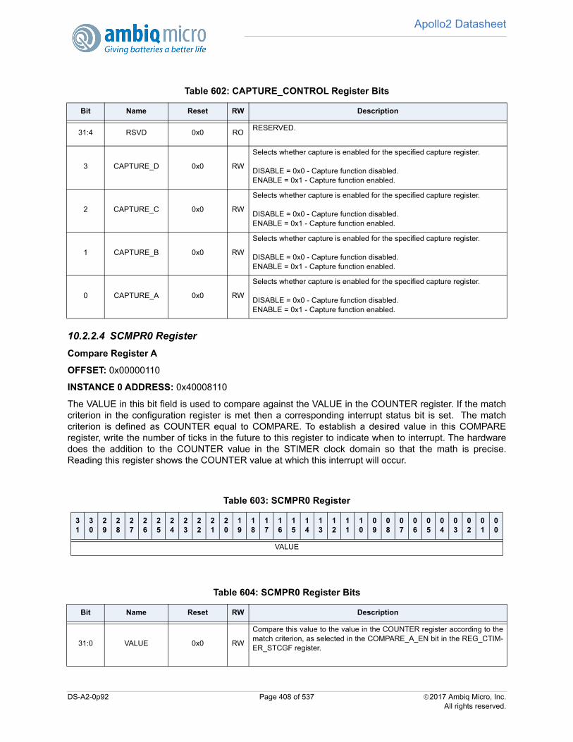
Apollo2 Datasheet
10.2.2.4 SCMPR0 Register
Compare Register A
OFFSET: 0x00000110
INSTANCE 0 ADDRESS: 0x40008110
The VALUE in this bit field is used to compare against the VALUE in the COUNTER register. If the matchcriterion in the configuration register is met then a corresponding interrupt status bit is set. The matchcriterion is defined as COUNTER equal to COMPARE. To establish a desired value in this COMPAREregister, write the number of ticks in the future to this register to indicate when to interrupt. The hardwaredoes the addition to the COUNTER value in the STIMER clock domain so that the math is precise.Reading this register shows the COUNTER value at which this interrupt will occur.
Table 602: CAPTURE_CONTROL Register Bits
Bit Name Reset RW Description
31:4 RSVD 0x0 RORESERVED.
3 CAPTURE_D 0x0 RW
Selects whether capture is enabled for the specified capture register.
DISABLE = 0x0 - Capture function disabled.ENABLE = 0x1 - Capture function enabled.
2 CAPTURE_C 0x0 RW
Selects whether capture is enabled for the specified capture register.
DISABLE = 0x0 - Capture function disabled.ENABLE = 0x1 - Capture function enabled.
1 CAPTURE_B 0x0 RW
Selects whether capture is enabled for the specified capture register.
DISABLE = 0x0 - Capture function disabled.ENABLE = 0x1 - Capture function enabled.
0 CAPTURE_A 0x0 RW
Selects whether capture is enabled for the specified capture register.
DISABLE = 0x0 - Capture function disabled.ENABLE = 0x1 - Capture function enabled.
Table 603: SCMPR0 Register
31
30
29
28
27
26
25
24
23
22
21
20
19
18
17
16
15
14
13
12
11
10
09
08
07
06
05
04
03
02
01
00
VALUE
Table 604: SCMPR0 Register Bits
Bit Name Reset RW Description
31:0 VALUE 0x0 RW
Compare this value to the value in the COUNTER register according to thematch criterion, as selected in the COMPARE_A_EN bit in the REG_CTIM-ER_STCGF register.
DS-A2-0p92 Page 408 of 537 2017 Ambiq Micro, Inc.All rights reserved.
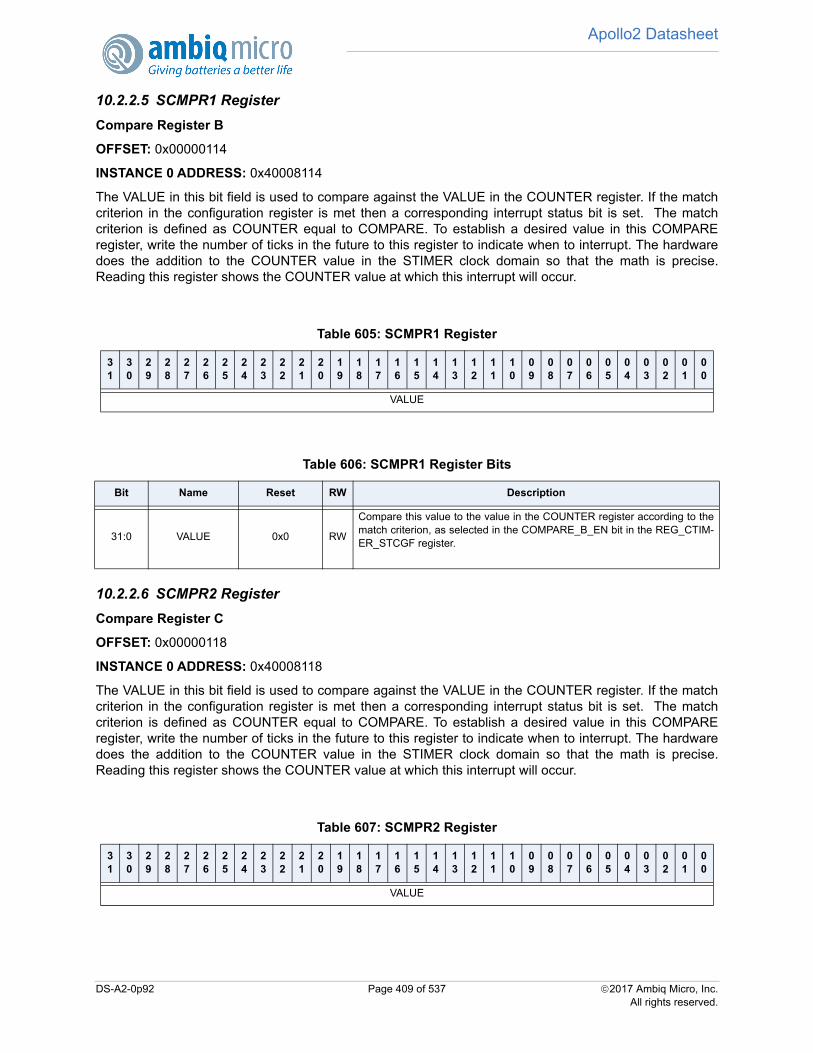
Apollo2 Datasheet
10.2.2.5 SCMPR1 Register
Compare Register B
OFFSET: 0x00000114
INSTANCE 0 ADDRESS: 0x40008114
The VALUE in this bit field is used to compare against the VALUE in the COUNTER register. If the matchcriterion in the configuration register is met then a corresponding interrupt status bit is set. The matchcriterion is defined as COUNTER equal to COMPARE. To establish a desired value in this COMPAREregister, write the number of ticks in the future to this register to indicate when to interrupt. The hardwaredoes the addition to the COUNTER value in the STIMER clock domain so that the math is precise.Reading this register shows the COUNTER value at which this interrupt will occur.
10.2.2.6 SCMPR2 Register
Compare Register C
OFFSET: 0x00000118
INSTANCE 0 ADDRESS: 0x40008118
The VALUE in this bit field is used to compare against the VALUE in the COUNTER register. If the matchcriterion in the configuration register is met then a corresponding interrupt status bit is set. The matchcriterion is defined as COUNTER equal to COMPARE. To establish a desired value in this COMPAREregister, write the number of ticks in the future to this register to indicate when to interrupt. The hardwaredoes the addition to the COUNTER value in the STIMER clock domain so that the math is precise.Reading this register shows the COUNTER value at which this interrupt will occur.
Table 605: SCMPR1 Register
31
30
29
28
27
26
25
24
23
22
21
20
19
18
17
16
15
14
13
12
11
10
09
08
07
06
05
04
03
02
01
00
VALUE
Table 606: SCMPR1 Register Bits
Bit Name Reset RW Description
31:0 VALUE 0x0 RW
Compare this value to the value in the COUNTER register according to thematch criterion, as selected in the COMPARE_B_EN bit in the REG_CTIM-ER_STCGF register.
Table 607: SCMPR2 Register
31
30
29
28
27
26
25
24
23
22
21
20
19
18
17
16
15
14
13
12
11
10
09
08
07
06
05
04
03
02
01
00
VALUE
DS-A2-0p92 Page 409 of 537 2017 Ambiq Micro, Inc.All rights reserved.

Apollo2 Datasheet
10.2.2.7 SCMPR3 Register
Compare Register D
OFFSET: 0x0000011C
INSTANCE 0 ADDRESS: 0x4000811C
The VALUE in this bit field is used to compare against the VALUE in the COUNTER register. If the matchcriterion in the configuration register is met then a corresponding interrupt status bit is set. The matchcriterion is defined as COUNTER equal to COMPARE. To establish a desired value in this COMPAREregister, write the number of ticks in the future to this register to indicate when to interrupt. The hardwaredoes the addition to the COUNTER value in the STIMER clock domain so that the math is precise.Reading this register shows the COUNTER value at which this interrupt will occur.
10.2.2.8 SCMPR4 Register
Compare Register E
OFFSET: 0x00000120
INSTANCE 0 ADDRESS: 0x40008120
The VALUE in this bit field is used to compare against the VALUE in the COUNTER register. If the matchcriterion in the configuration register is met then a corresponding interrupt status bit is set. The matchcriterion is defined as COUNTER equal to COMPARE. To establish a desired value in this COMPAREregister, write the number of ticks in the future to this register to indicate when to interrupt. The hardwaredoes the addition to the COUNTER value in the STIMER clock domain so that the math is precise.Reading this register shows the COUNTER value at which this interrupt will occur.
Table 608: SCMPR2 Register Bits
Bit Name Reset RW Description
31:0 VALUE 0x0 RW
Compare this value to the value in the COUNTER register according to thematch criterion, as selected in the COMPARE_C_EN bit in the REG_CTIM-ER_STCGF register.
Table 609: SCMPR3 Register
31
30
29
28
27
26
25
24
23
22
21
20
19
18
17
16
15
14
13
12
11
10
09
08
07
06
05
04
03
02
01
00
VALUE
Table 610: SCMPR3 Register Bits
Bit Name Reset RW Description
31:0 VALUE 0x0 RW
Compare this value to the value in the COUNTER register according to thematch criterion, as selected in the COMPARE_D_EN bit in the REG_CTIM-ER_STCGF register.
DS-A2-0p92 Page 410 of 537 2017 Ambiq Micro, Inc.All rights reserved.
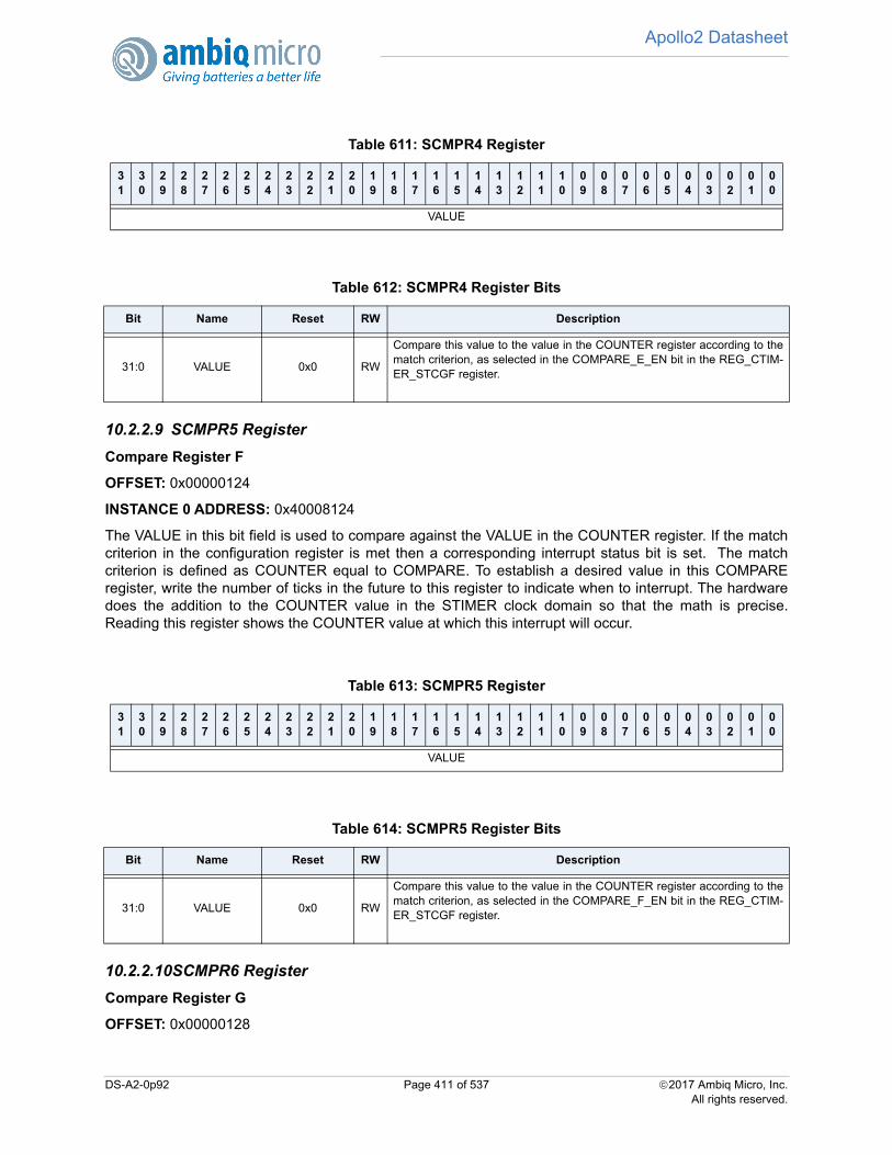
Apollo2 Datasheet
10.2.2.9 SCMPR5 Register
Compare Register F
OFFSET: 0x00000124
INSTANCE 0 ADDRESS: 0x40008124
The VALUE in this bit field is used to compare against the VALUE in the COUNTER register. If the matchcriterion in the configuration register is met then a corresponding interrupt status bit is set. The matchcriterion is defined as COUNTER equal to COMPARE. To establish a desired value in this COMPAREregister, write the number of ticks in the future to this register to indicate when to interrupt. The hardwaredoes the addition to the COUNTER value in the STIMER clock domain so that the math is precise.Reading this register shows the COUNTER value at which this interrupt will occur.
10.2.2.10SCMPR6 Register
Compare Register G
OFFSET: 0x00000128
Table 611: SCMPR4 Register
31
30
29
28
27
26
25
24
23
22
21
20
19
18
17
16
15
14
13
12
11
10
09
08
07
06
05
04
03
02
01
00
VALUE
Table 612: SCMPR4 Register Bits
Bit Name Reset RW Description
31:0 VALUE 0x0 RW
Compare this value to the value in the COUNTER register according to thematch criterion, as selected in the COMPARE_E_EN bit in the REG_CTIM-ER_STCGF register.
Table 613: SCMPR5 Register
31
30
29
28
27
26
25
24
23
22
21
20
19
18
17
16
15
14
13
12
11
10
09
08
07
06
05
04
03
02
01
00
VALUE
Table 614: SCMPR5 Register Bits
Bit Name Reset RW Description
31:0 VALUE 0x0 RW
Compare this value to the value in the COUNTER register according to thematch criterion, as selected in the COMPARE_F_EN bit in the REG_CTIM-ER_STCGF register.
DS-A2-0p92 Page 411 of 537 2017 Ambiq Micro, Inc.All rights reserved.

Apollo2 Datasheet
INSTANCE 0 ADDRESS: 0x40008128
The VALUE in this bit field is used to compare against the VALUE in the COUNTER register. If the matchcriterion in the configuration register is met then a corresponding interrupt status bit is set. The matchcriterion is defined as COUNTER equal to COMPARE. To establish a desired value in this COMPAREregister, write the number of ticks in the future to this register to indicate when to interrupt. The hardwaredoes the addition to the COUNTER value in the STIMER clock domain so that the math is precise.Reading this register shows the COUNTER value at which this interrupt will occur.
10.2.2.11SCMPR7 Register
Compare Register H
OFFSET: 0x0000012C
INSTANCE 0 ADDRESS: 0x4000812C
The VALUE in this bit field is used to compare against the VALUE in the COUNTER register. If the matchcriterion in the configuration register is met then a corresponding interrupt status bit is set. The matchcriterion is defined as COUNTER equal to COMPARE. To establish a desired value in this COMPAREregister, write the number of ticks in the future to this register to indicate when to interrupt. The hardwaredoes the addition to the COUNTER value in the STIMER clock domain so that the math is precise.
Table 615: SCMPR6 Register
31
30
29
28
27
26
25
24
23
22
21
20
19
18
17
16
15
14
13
12
11
10
09
08
07
06
05
04
03
02
01
00
VALUE
Table 616: SCMPR6 Register Bits
Bit Name Reset RW Description
31:0 VALUE 0x0 RW
Compare this value to the value in the COUNTER register according to thematch criterion, as selected in the COMPARE_G_EN bit in the REG_CTIM-ER_STCGF register.
Table 617: SCMPR7 Register
31
30
29
28
27
26
25
24
23
22
21
20
19
18
17
16
15
14
13
12
11
10
09
08
07
06
05
04
03
02
01
00
VALUE
DS-A2-0p92 Page 412 of 537 2017 Ambiq Micro, Inc.All rights reserved.
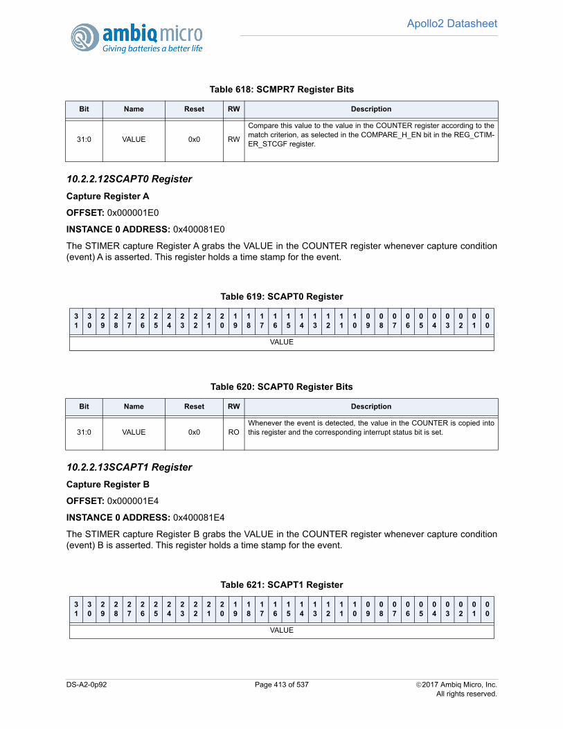
Apollo2 Datasheet
10.2.2.12SCAPT0 Register
Capture Register A
OFFSET: 0x000001E0
INSTANCE 0 ADDRESS: 0x400081E0
The STIMER capture Register A grabs the VALUE in the COUNTER register whenever capture condition(event) A is asserted. This register holds a time stamp for the event.
10.2.2.13SCAPT1 Register
Capture Register B
OFFSET: 0x000001E4
INSTANCE 0 ADDRESS: 0x400081E4
The STIMER capture Register B grabs the VALUE in the COUNTER register whenever capture condition(event) B is asserted. This register holds a time stamp for the event.
Table 618: SCMPR7 Register Bits
Bit Name Reset RW Description
31:0 VALUE 0x0 RW
Compare this value to the value in the COUNTER register according to thematch criterion, as selected in the COMPARE_H_EN bit in the REG_CTIM-ER_STCGF register.
Table 619: SCAPT0 Register
31
30
29
28
27
26
25
24
23
22
21
20
19
18
17
16
15
14
13
12
11
10
09
08
07
06
05
04
03
02
01
00
VALUE
Table 620: SCAPT0 Register Bits
Bit Name Reset RW Description
31:0 VALUE 0x0 ROWhenever the event is detected, the value in the COUNTER is copied intothis register and the corresponding interrupt status bit is set.
Table 621: SCAPT1 Register
31
30
29
28
27
26
25
24
23
22
21
20
19
18
17
16
15
14
13
12
11
10
09
08
07
06
05
04
03
02
01
00
VALUE
DS-A2-0p92 Page 413 of 537 2017 Ambiq Micro, Inc.All rights reserved.

Apollo2 Datasheet
10.2.2.14SCAPT2 Register
Capture Register C
OFFSET: 0x000001E8
INSTANCE 0 ADDRESS: 0x400081E8
The STIMER capture Register C grabs the VALUE in the COUNTER register whenever capture condition(event) C is asserted. This register holds a time stamp for the event.
10.2.2.15SCAPT3 Register
Capture Register D
OFFSET: 0x000001EC
INSTANCE 0 ADDRESS: 0x400081EC
The STIMER capture Register D grabs the VALUE in the COUNTER register whenever capture condition(event) D is asserted. This register holds a time stamp for the event.
Table 622: SCAPT1 Register Bits
Bit Name Reset RW Description
31:0 VALUE 0x0 ROWhenever the event is detected, the value in the COUNTER is copied intothis register and the corresponding interrupt status bit is set.
Table 623: SCAPT2 Register
31
30
29
28
27
26
25
24
23
22
21
20
19
18
17
16
15
14
13
12
11
10
09
08
07
06
05
04
03
02
01
00
VALUE
Table 624: SCAPT2 Register Bits
Bit Name Reset RW Description
31:0 VALUE 0x0 ROWhenever the event is detected, the value in the COUNTER is copied intothis register and the corresponding interrupt status bit is set.
Table 625: SCAPT3 Register
31
30
29
28
27
26
25
24
23
22
21
20
19
18
17
16
15
14
13
12
11
10
09
08
07
06
05
04
03
02
01
00
VALUE
DS-A2-0p92 Page 414 of 537 2017 Ambiq Micro, Inc.All rights reserved.
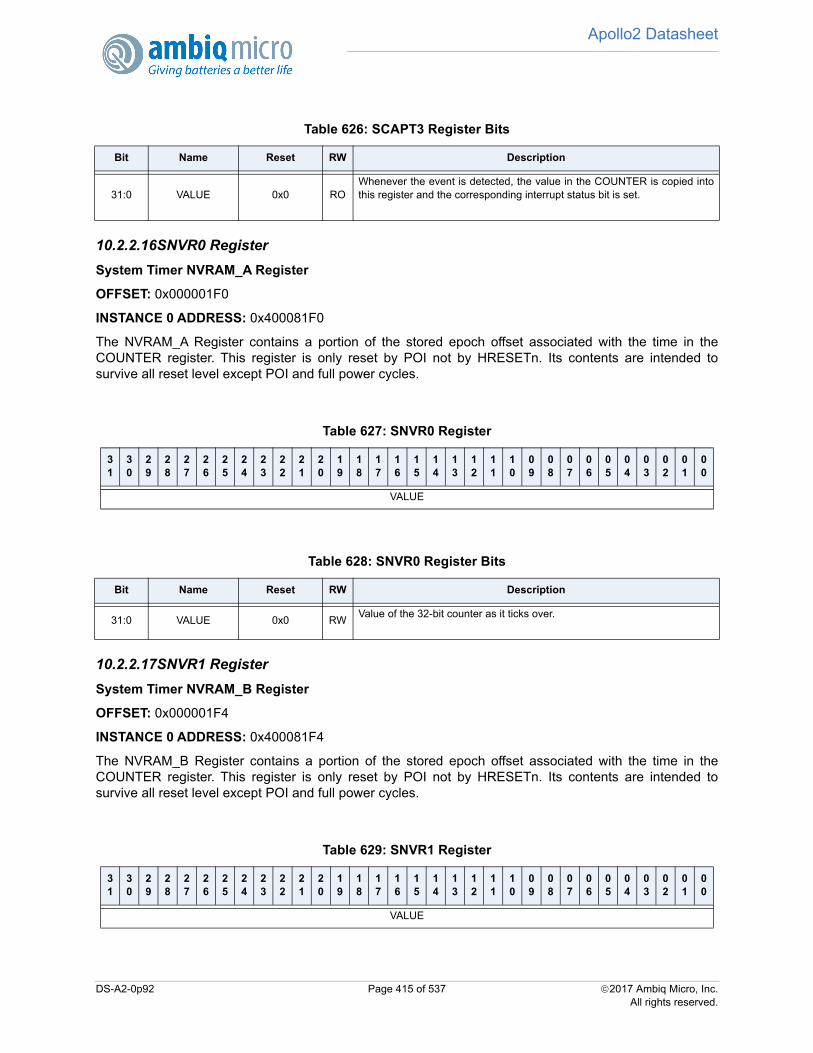
Apollo2 Datasheet
10.2.2.16SNVR0 Register
System Timer NVRAM_A Register
OFFSET: 0x000001F0
INSTANCE 0 ADDRESS: 0x400081F0
The NVRAM_A Register contains a portion of the stored epoch offset associated with the time in theCOUNTER register. This register is only reset by POI not by HRESETn. Its contents are intended tosurvive all reset level except POI and full power cycles.
10.2.2.17SNVR1 Register
System Timer NVRAM_B Register
OFFSET: 0x000001F4
INSTANCE 0 ADDRESS: 0x400081F4
The NVRAM_B Register contains a portion of the stored epoch offset associated with the time in theCOUNTER register. This register is only reset by POI not by HRESETn. Its contents are intended tosurvive all reset level except POI and full power cycles.
Table 626: SCAPT3 Register Bits
Bit Name Reset RW Description
31:0 VALUE 0x0 ROWhenever the event is detected, the value in the COUNTER is copied intothis register and the corresponding interrupt status bit is set.
Table 627: SNVR0 Register
31
30
29
28
27
26
25
24
23
22
21
20
19
18
17
16
15
14
13
12
11
10
09
08
07
06
05
04
03
02
01
00
VALUE
Table 628: SNVR0 Register Bits
Bit Name Reset RW Description
31:0 VALUE 0x0 RWValue of the 32-bit counter as it ticks over.
Table 629: SNVR1 Register
31
30
29
28
27
26
25
24
23
22
21
20
19
18
17
16
15
14
13
12
11
10
09
08
07
06
05
04
03
02
01
00
VALUE
DS-A2-0p92 Page 415 of 537 2017 Ambiq Micro, Inc.All rights reserved.

Apollo2 Datasheet
10.2.2.18SNVR2 Register
System Timer NVRAM_C Register
OFFSET: 0x000001F8
INSTANCE 0 ADDRESS: 0x400081F8
The NVRAM_C Register contains a portion of the stored epoch offset associated with the time in theCOUNTER register. This register is only reset by POI not by HRESETn. Its contents are intended tosurvive all reset level except POI and full power cycles.
10.2.2.19STMINTEN Register
STIMER Interrupt registers: Enable
OFFSET: 0x00000300
INSTANCE 0 ADDRESS: 0x40008300
Set bits in this register to allow this module to generate the corresponding interrupt.
Table 630: SNVR1 Register Bits
Bit Name Reset RW Description
31:0 VALUE 0x0 RWValue of the 32-bit counter as it ticks over.
Table 631: SNVR2 Register
31
30
29
28
27
26
25
24
23
22
21
20
19
18
17
16
15
14
13
12
11
10
09
08
07
06
05
04
03
02
01
00
VALUE
Table 632: SNVR2 Register Bits
Bit Name Reset RW Description
31:0 VALUE 0x0 RWValue of the 32-bit counter as it ticks over.
Table 633: STMINTEN Register
31
30
29
28
27
26
25
24
23
22
21
20
19
18
17
16
15
14
13
12
11
10
09
08
07
06
05
04
03
02
01
00
RSVD
CA
PT
UR
ED
CA
PT
UR
EC
CA
PT
UR
EB
CA
PT
UR
EA
OV
ER
FLO
W
CO
MP
AR
EH
CO
MP
AR
EG
CO
MP
AR
EF
CO
MP
AR
EE
CO
MP
AR
ED
CO
MP
AR
EC
CO
MP
AR
EB
CO
MP
AR
EA
DS-A2-0p92 Page 416 of 537 2017 Ambiq Micro, Inc.All rights reserved.
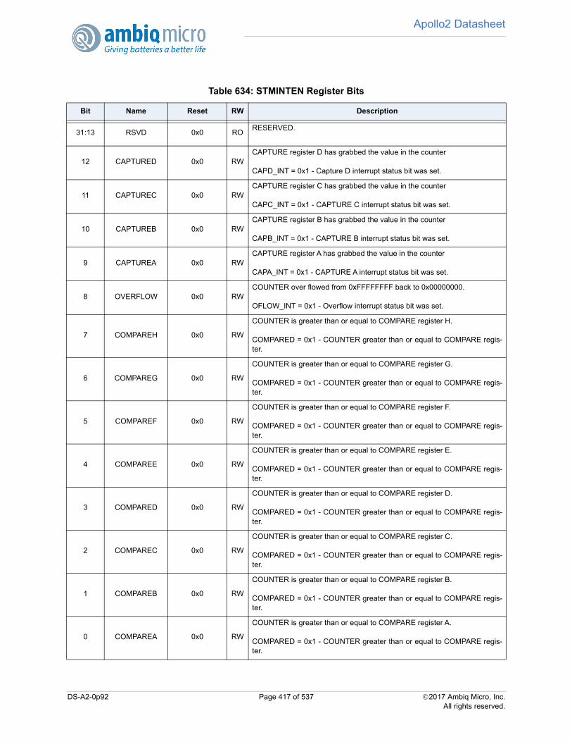
Apollo2 Datasheet
Table 634: STMINTEN Register Bits
Bit Name Reset RW Description
31:13 RSVD 0x0 RORESERVED.
12 CAPTURED 0x0 RWCAPTURE register D has grabbed the value in the counter
CAPD_INT = 0x1 - Capture D interrupt status bit was set.
11 CAPTUREC 0x0 RWCAPTURE register C has grabbed the value in the counter
CAPC_INT = 0x1 - CAPTURE C interrupt status bit was set.
10 CAPTUREB 0x0 RWCAPTURE register B has grabbed the value in the counter
CAPB_INT = 0x1 - CAPTURE B interrupt status bit was set.
9 CAPTUREA 0x0 RWCAPTURE register A has grabbed the value in the counter
CAPA_INT = 0x1 - CAPTURE A interrupt status bit was set.
8 OVERFLOW 0x0 RWCOUNTER over flowed from 0xFFFFFFFF back to 0x00000000.
OFLOW_INT = 0x1 - Overflow interrupt status bit was set.
7 COMPAREH 0x0 RW
COUNTER is greater than or equal to COMPARE register H.
COMPARED = 0x1 - COUNTER greater than or equal to COMPARE regis-ter.
6 COMPAREG 0x0 RW
COUNTER is greater than or equal to COMPARE register G.
COMPARED = 0x1 - COUNTER greater than or equal to COMPARE regis-ter.
5 COMPAREF 0x0 RW
COUNTER is greater than or equal to COMPARE register F.
COMPARED = 0x1 - COUNTER greater than or equal to COMPARE regis-ter.
4 COMPAREE 0x0 RW
COUNTER is greater than or equal to COMPARE register E.
COMPARED = 0x1 - COUNTER greater than or equal to COMPARE regis-ter.
3 COMPARED 0x0 RW
COUNTER is greater than or equal to COMPARE register D.
COMPARED = 0x1 - COUNTER greater than or equal to COMPARE regis-ter.
2 COMPAREC 0x0 RW
COUNTER is greater than or equal to COMPARE register C.
COMPARED = 0x1 - COUNTER greater than or equal to COMPARE regis-ter.
1 COMPAREB 0x0 RW
COUNTER is greater than or equal to COMPARE register B.
COMPARED = 0x1 - COUNTER greater than or equal to COMPARE regis-ter.
0 COMPAREA 0x0 RW
COUNTER is greater than or equal to COMPARE register A.
COMPARED = 0x1 - COUNTER greater than or equal to COMPARE regis-ter.
DS-A2-0p92 Page 417 of 537 2017 Ambiq Micro, Inc.All rights reserved.
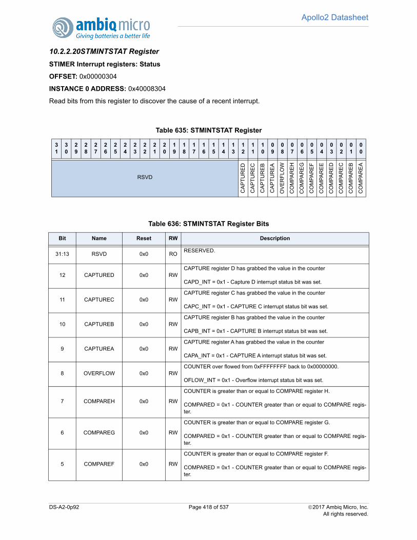
Apollo2 Datasheet
10.2.2.20STMINTSTAT Register
STIMER Interrupt registers: Status
OFFSET: 0x00000304
INSTANCE 0 ADDRESS: 0x40008304
Read bits from this register to discover the cause of a recent interrupt.
Table 635: STMINTSTAT Register
31
30
29
28
27
26
25
24
23
22
21
20
19
18
17
16
15
14
13
12
11
10
09
08
07
06
05
04
03
02
01
00
RSVD
CA
PT
UR
ED
CA
PT
UR
EC
CA
PT
UR
EB
CA
PT
UR
EA
OV
ER
FL
OW
CO
MP
AR
EH
CO
MP
AR
EG
CO
MP
AR
EF
CO
MP
AR
EE
CO
MP
AR
ED
CO
MP
AR
EC
CO
MP
AR
EB
CO
MP
AR
EA
Table 636: STMINTSTAT Register Bits
Bit Name Reset RW Description
31:13 RSVD 0x0 RORESERVED.
12 CAPTURED 0x0 RWCAPTURE register D has grabbed the value in the counter
CAPD_INT = 0x1 - Capture D interrupt status bit was set.
11 CAPTUREC 0x0 RWCAPTURE register C has grabbed the value in the counter
CAPC_INT = 0x1 - CAPTURE C interrupt status bit was set.
10 CAPTUREB 0x0 RWCAPTURE register B has grabbed the value in the counter
CAPB_INT = 0x1 - CAPTURE B interrupt status bit was set.
9 CAPTUREA 0x0 RWCAPTURE register A has grabbed the value in the counter
CAPA_INT = 0x1 - CAPTURE A interrupt status bit was set.
8 OVERFLOW 0x0 RWCOUNTER over flowed from 0xFFFFFFFF back to 0x00000000.
OFLOW_INT = 0x1 - Overflow interrupt status bit was set.
7 COMPAREH 0x0 RW
COUNTER is greater than or equal to COMPARE register H.
COMPARED = 0x1 - COUNTER greater than or equal to COMPARE regis-ter.
6 COMPAREG 0x0 RW
COUNTER is greater than or equal to COMPARE register G.
COMPARED = 0x1 - COUNTER greater than or equal to COMPARE regis-ter.
5 COMPAREF 0x0 RW
COUNTER is greater than or equal to COMPARE register F.
COMPARED = 0x1 - COUNTER greater than or equal to COMPARE regis-ter.
DS-A2-0p92 Page 418 of 537 2017 Ambiq Micro, Inc.All rights reserved.
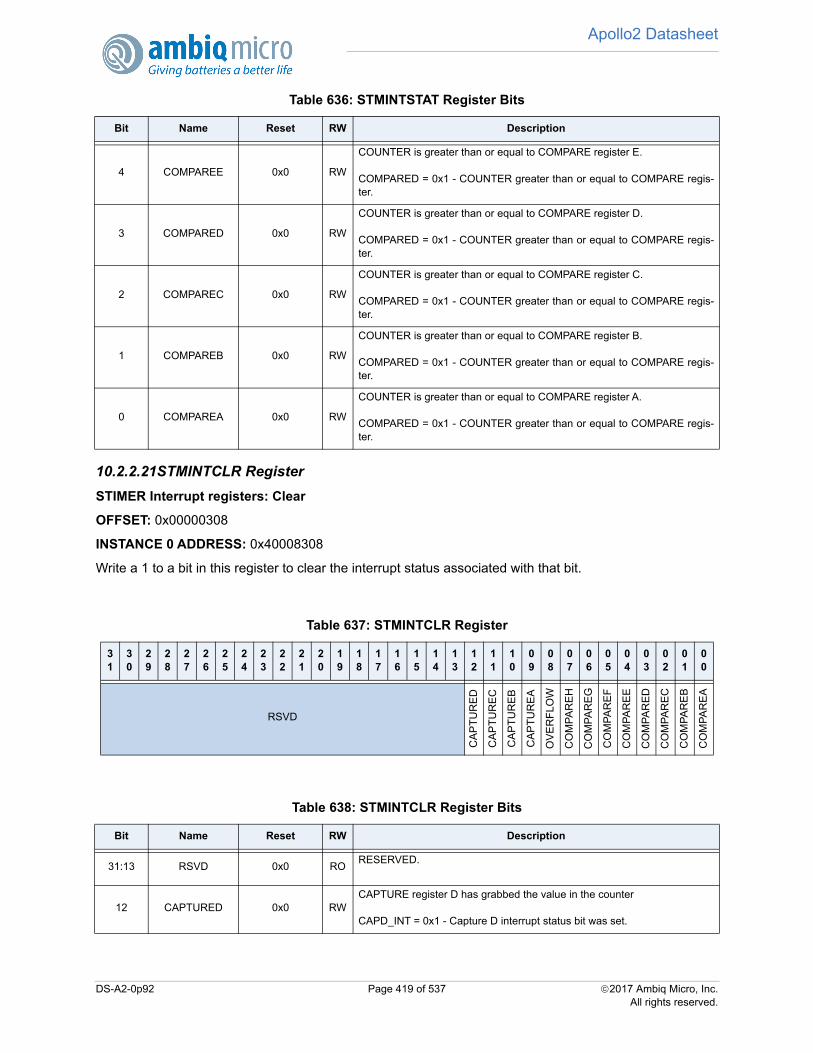
Apollo2 Datasheet
10.2.2.21STMINTCLR Register
STIMER Interrupt registers: Clear
OFFSET: 0x00000308
INSTANCE 0 ADDRESS: 0x40008308
Write a 1 to a bit in this register to clear the interrupt status associated with that bit.
4 COMPAREE 0x0 RW
COUNTER is greater than or equal to COMPARE register E.
COMPARED = 0x1 - COUNTER greater than or equal to COMPARE regis-ter.
3 COMPARED 0x0 RW
COUNTER is greater than or equal to COMPARE register D.
COMPARED = 0x1 - COUNTER greater than or equal to COMPARE regis-ter.
2 COMPAREC 0x0 RW
COUNTER is greater than or equal to COMPARE register C.
COMPARED = 0x1 - COUNTER greater than or equal to COMPARE regis-ter.
1 COMPAREB 0x0 RW
COUNTER is greater than or equal to COMPARE register B.
COMPARED = 0x1 - COUNTER greater than or equal to COMPARE regis-ter.
0 COMPAREA 0x0 RW
COUNTER is greater than or equal to COMPARE register A.
COMPARED = 0x1 - COUNTER greater than or equal to COMPARE regis-ter.
Table 637: STMINTCLR Register
31
30
29
28
27
26
25
24
23
22
21
20
19
18
17
16
15
14
13
12
11
10
09
08
07
06
05
04
03
02
01
00
RSVD
CA
PT
UR
ED
CA
PT
UR
EC
CA
PT
UR
EB
CA
PT
UR
EA
OV
ER
FLO
W
CO
MP
AR
EH
CO
MP
AR
EG
CO
MP
AR
EF
CO
MP
AR
EE
CO
MP
AR
ED
CO
MP
AR
EC
CO
MP
AR
EB
CO
MP
AR
EA
Table 638: STMINTCLR Register Bits
Bit Name Reset RW Description
31:13 RSVD 0x0 RORESERVED.
12 CAPTURED 0x0 RWCAPTURE register D has grabbed the value in the counter
CAPD_INT = 0x1 - Capture D interrupt status bit was set.
Table 636: STMINTSTAT Register Bits
Bit Name Reset RW Description
DS-A2-0p92 Page 419 of 537 2017 Ambiq Micro, Inc.All rights reserved.
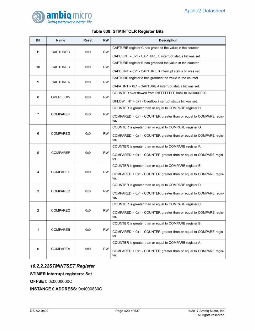
Apollo2 Datasheet
10.2.2.22STMINTSET Register
STIMER Interrupt registers: Set
OFFSET: 0x0000030C
INSTANCE 0 ADDRESS: 0x4000830C
11 CAPTUREC 0x0 RWCAPTURE register C has grabbed the value in the counter
CAPC_INT = 0x1 - CAPTURE C interrupt status bit was set.
10 CAPTUREB 0x0 RWCAPTURE register B has grabbed the value in the counter
CAPB_INT = 0x1 - CAPTURE B interrupt status bit was set.
9 CAPTUREA 0x0 RWCAPTURE register A has grabbed the value in the counter
CAPA_INT = 0x1 - CAPTURE A interrupt status bit was set.
8 OVERFLOW 0x0 RWCOUNTER over flowed from 0xFFFFFFFF back to 0x00000000.
OFLOW_INT = 0x1 - Overflow interrupt status bit was set.
7 COMPAREH 0x0 RW
COUNTER is greater than or equal to COMPARE register H.
COMPARED = 0x1 - COUNTER greater than or equal to COMPARE regis-ter.
6 COMPAREG 0x0 RW
COUNTER is greater than or equal to COMPARE register G.
COMPARED = 0x1 - COUNTER greater than or equal to COMPARE regis-ter.
5 COMPAREF 0x0 RW
COUNTER is greater than or equal to COMPARE register F.
COMPARED = 0x1 - COUNTER greater than or equal to COMPARE regis-ter.
4 COMPAREE 0x0 RW
COUNTER is greater than or equal to COMPARE register E.
COMPARED = 0x1 - COUNTER greater than or equal to COMPARE regis-ter.
3 COMPARED 0x0 RW
COUNTER is greater than or equal to COMPARE register D.
COMPARED = 0x1 - COUNTER greater than or equal to COMPARE regis-ter.
2 COMPAREC 0x0 RW
COUNTER is greater than or equal to COMPARE register C.
COMPARED = 0x1 - COUNTER greater than or equal to COMPARE regis-ter.
1 COMPAREB 0x0 RW
COUNTER is greater than or equal to COMPARE register B.
COMPARED = 0x1 - COUNTER greater than or equal to COMPARE regis-ter.
0 COMPAREA 0x0 RW
COUNTER is greater than or equal to COMPARE register A.
COMPARED = 0x1 - COUNTER greater than or equal to COMPARE regis-ter.
Table 638: STMINTCLR Register Bits
Bit Name Reset RW Description
DS-A2-0p92 Page 420 of 537 2017 Ambiq Micro, Inc.All rights reserved.
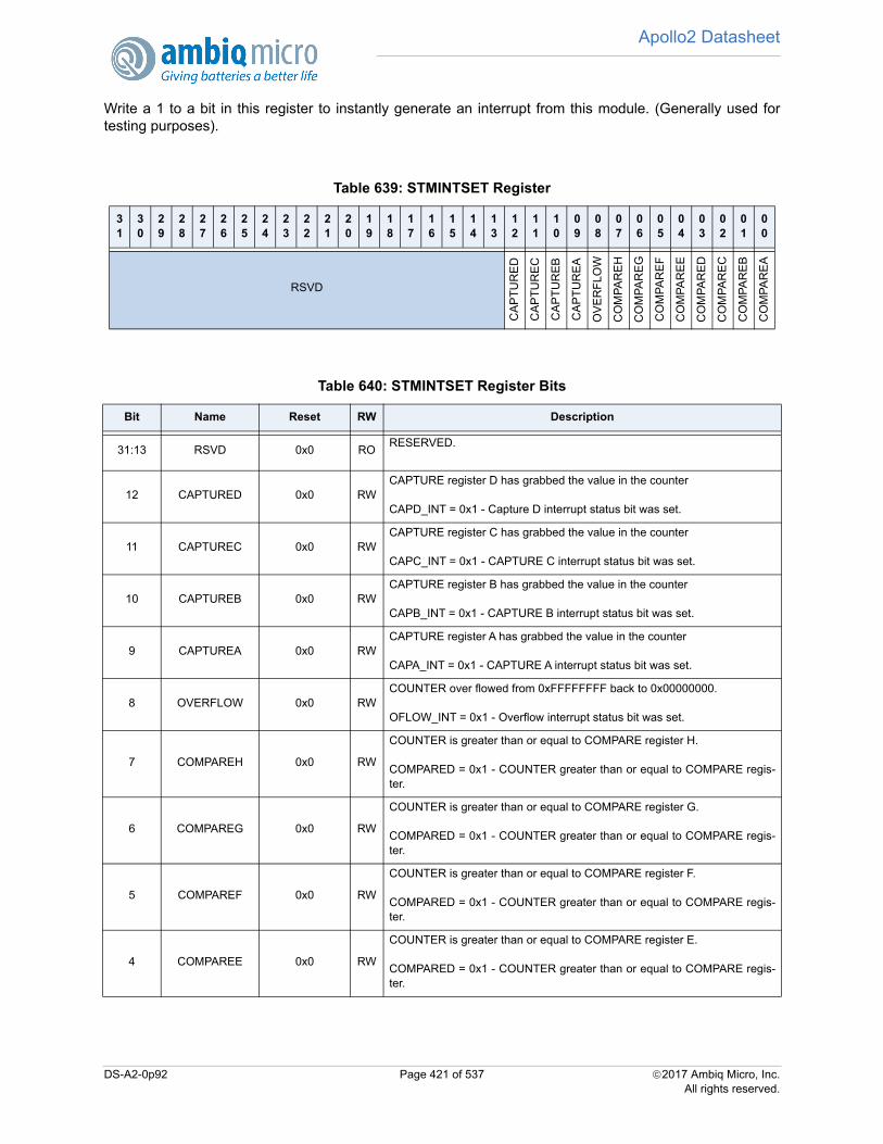
Apollo2 Datasheet
Write a 1 to a bit in this register to instantly generate an interrupt from this module. (Generally used fortesting purposes).
Table 639: STMINTSET Register
31
30
29
28
27
26
25
24
23
22
21
20
19
18
17
16
15
14
13
12
11
10
09
08
07
06
05
04
03
02
01
00
RSVD
CA
PT
UR
ED
CA
PT
UR
EC
CA
PT
UR
EB
CA
PT
UR
EA
OV
ER
FLO
W
CO
MP
AR
EH
CO
MP
AR
EG
CO
MP
AR
EF
CO
MP
AR
EE
CO
MP
AR
ED
CO
MP
AR
EC
CO
MP
AR
EB
CO
MP
AR
EA
Table 640: STMINTSET Register Bits
Bit Name Reset RW Description
31:13 RSVD 0x0 RORESERVED.
12 CAPTURED 0x0 RWCAPTURE register D has grabbed the value in the counter
CAPD_INT = 0x1 - Capture D interrupt status bit was set.
11 CAPTUREC 0x0 RWCAPTURE register C has grabbed the value in the counter
CAPC_INT = 0x1 - CAPTURE C interrupt status bit was set.
10 CAPTUREB 0x0 RWCAPTURE register B has grabbed the value in the counter
CAPB_INT = 0x1 - CAPTURE B interrupt status bit was set.
9 CAPTUREA 0x0 RWCAPTURE register A has grabbed the value in the counter
CAPA_INT = 0x1 - CAPTURE A interrupt status bit was set.
8 OVERFLOW 0x0 RWCOUNTER over flowed from 0xFFFFFFFF back to 0x00000000.
OFLOW_INT = 0x1 - Overflow interrupt status bit was set.
7 COMPAREH 0x0 RW
COUNTER is greater than or equal to COMPARE register H.
COMPARED = 0x1 - COUNTER greater than or equal to COMPARE regis-ter.
6 COMPAREG 0x0 RW
COUNTER is greater than or equal to COMPARE register G.
COMPARED = 0x1 - COUNTER greater than or equal to COMPARE regis-ter.
5 COMPAREF 0x0 RW
COUNTER is greater than or equal to COMPARE register F.
COMPARED = 0x1 - COUNTER greater than or equal to COMPARE regis-ter.
4 COMPAREE 0x0 RW
COUNTER is greater than or equal to COMPARE register E.
COMPARED = 0x1 - COUNTER greater than or equal to COMPARE regis-ter.
DS-A2-0p92 Page 421 of 537 2017 Ambiq Micro, Inc.All rights reserved.
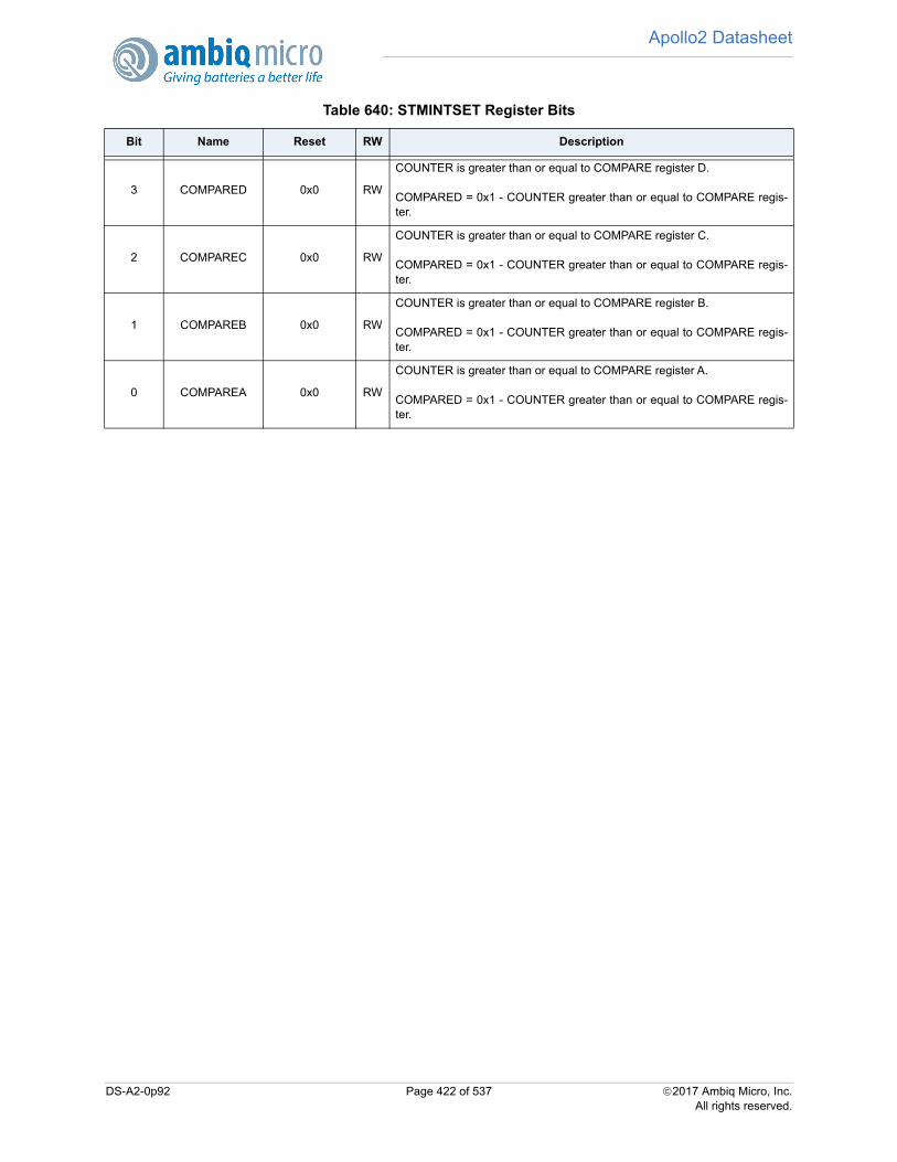
Apollo2 Datasheet
3 COMPARED 0x0 RW
COUNTER is greater than or equal to COMPARE register D.
COMPARED = 0x1 - COUNTER greater than or equal to COMPARE regis-ter.
2 COMPAREC 0x0 RW
COUNTER is greater than or equal to COMPARE register C.
COMPARED = 0x1 - COUNTER greater than or equal to COMPARE regis-ter.
1 COMPAREB 0x0 RW
COUNTER is greater than or equal to COMPARE register B.
COMPARED = 0x1 - COUNTER greater than or equal to COMPARE regis-ter.
0 COMPAREA 0x0 RW
COUNTER is greater than or equal to COMPARE register A.
COMPARED = 0x1 - COUNTER greater than or equal to COMPARE regis-ter.
Table 640: STMINTSET Register Bits
Bit Name Reset RW Description
DS-A2-0p92 Page 422 of 537 2017 Ambiq Micro, Inc.All rights reserved.
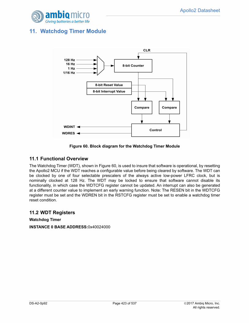
Apollo2 Datasheet
11. Watchdog Timer Module
Figure 60. Block diagram for the Watchdog Timer Module
11.1 Functional OverviewThe Watchdog Timer (WDT), shown in Figure 60, is used to insure that software is operational, by resettingthe Apollo2 MCU if the WDT reaches a configurable value before being cleared by software. The WDT canbe clocked by one of four selectable prescalers of the always active low-power LFRC clock, but isnominally clocked at 128 Hz. The WDT may be locked to ensure that software cannot disable itsfunctionality, in which case the WDTCFG register cannot be updated. An interrupt can also be generatedat a different counter value to implement an early warning function. Note: The RESEN bit in the WDTCFGregister must be set and the WDREN bit in the RSTCFG register must be set to enable a watchdog timerreset condition.
11.2 WDT RegistersWatchdog Timer
INSTANCE 0 BASE ADDRESS:0x40024000
8-bit Counter
128 Hz
8-bit Reset Value
Compare
ControlWDINT
WDRES
CLR
8-bit Interrupt Value
Compare
16 Hz1 Hz
1/16 Hz
DS-A2-0p92 Page 423 of 537 2017 Ambiq Micro, Inc.All rights reserved.
Apollo2 Datasheet
11.2.1 Register Memory Map
Table 641: WDT Register Map
Address(s) Register Name Description
0x40024000 CFG Configuration Register
0x40024004 RSTRT Restart the watchdog timer
0x40024008 LOCK Locks the WDT
0x4002400C COUNT Current Counter Value for WDT
0x40024200 INTEN WDT Interrupt register: Enable
0x40024204 INTSTAT WDT Interrupt register: Status
0x40024208 INTCLR WDT Interrupt register: Clear
0x4002420C INTSET WDT Interrupt register: Set
DS-A2-0p92 Page 424 of 537 2017 Ambiq Micro, Inc.All rights reserved.
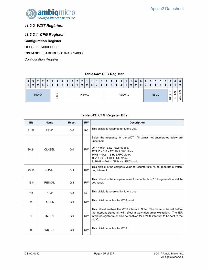
Apollo2 Datasheet
11.2.2 WDT Registers
11.2.2.1 CFG Register
Configuration Register
OFFSET: 0x00000000
INSTANCE 0 ADDRESS: 0x40024000
Configuration Register
Table 642: CFG Register
31
30
29
28
27
26
25
24
23
22
21
20
19
18
17
16
15
14
13
12
11
10
09
08
07
06
05
04
03
02
01
00
RSVD
CL
KS
EL
INTVAL RESVAL RSVD
RE
SE
N
INT
EN
WD
TE
N
Table 643: CFG Register Bits
Bit Name Reset RW Description
31:27 RSVD 0x0 ROThis bitfield is reserved for future use.
26:24 CLKSEL 0x0 RW
Select the frequency for the WDT. All values not enumerated below areundefined.
OFF = 0x0 - Low Power Mode.128HZ = 0x1 - 128 Hz LFRC clock.16HZ = 0x2 - 16 Hz LFRC clock.1HZ = 0x3 - 1 Hz LFRC clock.1_16HZ = 0x4 - 1/16th Hz LFRC clock.
23:16 INTVAL 0xff RWThis bitfield is the compare value for counter bits 7:0 to generate a watch-dog interrupt.
15:8 RESVAL 0xff RWThis bitfield is the compare value for counter bits 7:0 to generate a watch-dog reset.
7:3 RSVD 0x0 ROThis bitfield is reserved for future use.
2 RESEN 0x0 RWThis bitfield enables the WDT reset.
1 INTEN 0x0 RW
This bitfield enables the WDT interrupt. Note : This bit must be set beforethe interrupt status bit will reflect a watchdog timer expiration. The IERinterrupt register must also be enabled for a WDT interrupt to be sent to theNVIC.
0 WDTEN 0x0 RWThis bitfield enables the WDT.
DS-A2-0p92 Page 425 of 537 2017 Ambiq Micro, Inc.All rights reserved.
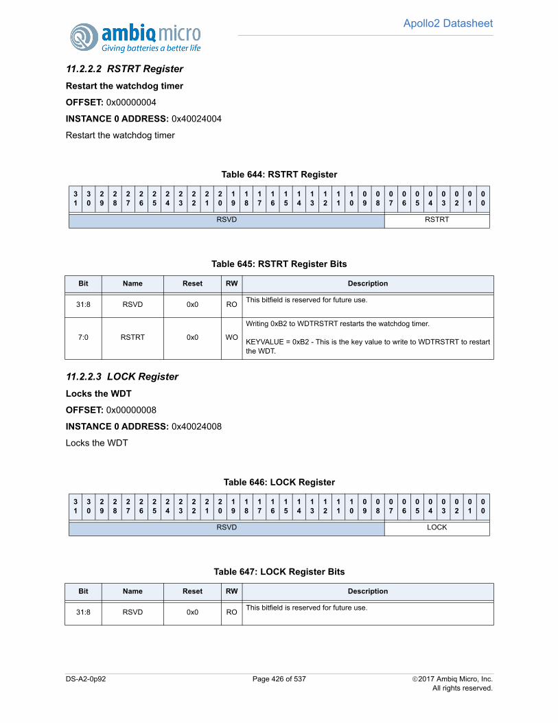
Apollo2 Datasheet
11.2.2.2 RSTRT Register
Restart the watchdog timer
OFFSET: 0x00000004
INSTANCE 0 ADDRESS: 0x40024004
Restart the watchdog timer
11.2.2.3 LOCK Register
Locks the WDT
OFFSET: 0x00000008
INSTANCE 0 ADDRESS: 0x40024008
Locks the WDT
Table 644: RSTRT Register
31
30
29
28
27
26
25
24
23
22
21
20
19
18
17
16
15
14
13
12
11
10
09
08
07
06
05
04
03
02
01
00
RSVD RSTRT
Table 645: RSTRT Register Bits
Bit Name Reset RW Description
31:8 RSVD 0x0 ROThis bitfield is reserved for future use.
7:0 RSTRT 0x0 WO
Writing 0xB2 to WDTRSTRT restarts the watchdog timer.
KEYVALUE = 0xB2 - This is the key value to write to WDTRSTRT to restartthe WDT.
Table 646: LOCK Register
31
30
29
28
27
26
25
24
23
22
21
20
19
18
17
16
15
14
13
12
11
10
09
08
07
06
05
04
03
02
01
00
RSVD LOCK
Table 647: LOCK Register Bits
Bit Name Reset RW Description
31:8 RSVD 0x0 ROThis bitfield is reserved for future use.
DS-A2-0p92 Page 426 of 537 2017 Ambiq Micro, Inc.All rights reserved.

Apollo2 Datasheet
11.2.2.4 COUNT Register
Current Counter Value for WDT
OFFSET: 0x0000000C
INSTANCE 0 ADDRESS: 0x4002400C
Current Counter Value for WDT
11.2.2.5 INTEN Register
WDT Interrupt register: Enable
OFFSET: 0x00000200
INSTANCE 0 ADDRESS: 0x40024200
Set bits in this register to allow this module to generate the corresponding interrupt.
7:0 LOCK 0x0 WO
Writing 0x3A locks the watchdog timer. Once locked, the WDTCFG reg can-not be written and WDTEN is set.
KEYVALUE = 0x3A - This is the key value to write to WDTLOCK to lock theWDT.
Table 648: COUNT Register
31
30
29
28
27
26
25
24
23
22
21
20
19
18
17
16
15
14
13
12
11
10
09
08
07
06
05
04
03
02
01
00
RSVD COUNT
Table 649: COUNT Register Bits
Bit Name Reset RW Description
31:8 RSVD 0x0 ROThis bitfield is reserved for future use.
7:0 COUNT 0x0 RORead-Only current value of the WDT counter
Table 650: INTEN Register
31
30
29
28
27
26
25
24
23
22
21
20
19
18
17
16
15
14
13
12
11
10
09
08
07
06
05
04
03
02
01
00
RSVD
WD
T
Table 647: LOCK Register Bits
Bit Name Reset RW Description
DS-A2-0p92 Page 427 of 537 2017 Ambiq Micro, Inc.All rights reserved.
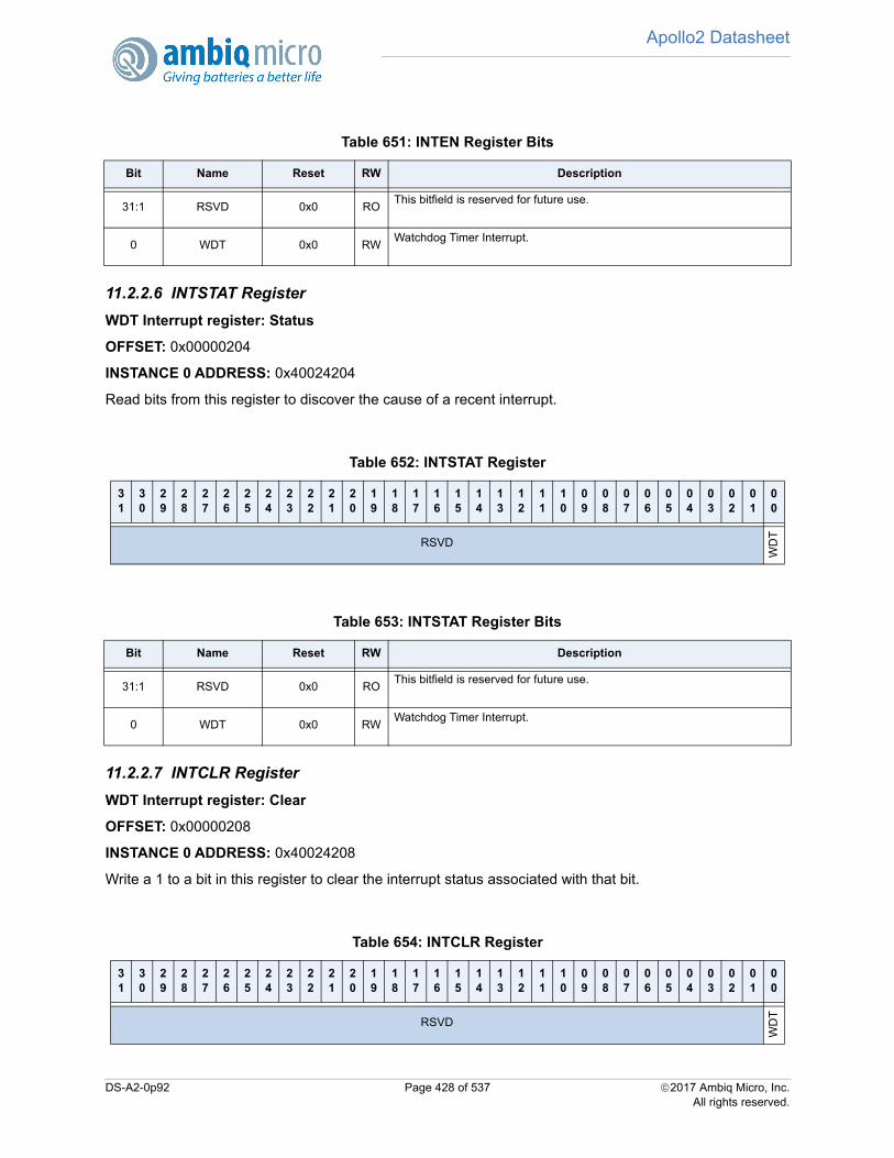
Apollo2 Datasheet
11.2.2.6 INTSTAT Register
WDT Interrupt register: Status
OFFSET: 0x00000204
INSTANCE 0 ADDRESS: 0x40024204
Read bits from this register to discover the cause of a recent interrupt.
11.2.2.7 INTCLR Register
WDT Interrupt register: Clear
OFFSET: 0x00000208
INSTANCE 0 ADDRESS: 0x40024208
Write a 1 to a bit in this register to clear the interrupt status associated with that bit.
Table 651: INTEN Register Bits
Bit Name Reset RW Description
31:1 RSVD 0x0 ROThis bitfield is reserved for future use.
0 WDT 0x0 RWWatchdog Timer Interrupt.
Table 652: INTSTAT Register
31
30
29
28
27
26
25
24
23
22
21
20
19
18
17
16
15
14
13
12
11
10
09
08
07
06
05
04
03
02
01
00
RSVD
WD
T
Table 653: INTSTAT Register Bits
Bit Name Reset RW Description
31:1 RSVD 0x0 ROThis bitfield is reserved for future use.
0 WDT 0x0 RWWatchdog Timer Interrupt.
Table 654: INTCLR Register
31
30
29
28
27
26
25
24
23
22
21
20
19
18
17
16
15
14
13
12
11
10
09
08
07
06
05
04
03
02
01
00
RSVD
WD
T
DS-A2-0p92 Page 428 of 537 2017 Ambiq Micro, Inc.All rights reserved.

Apollo2 Datasheet
11.2.2.8 INTSET Register
WDT Interrupt register: Set
OFFSET: 0x0000020C
INSTANCE 0 ADDRESS: 0x4002420C
Write a 1 to a bit in this register to instantly generate an interrupt from this module. (Generally used fortesting purposes).
Table 655: INTCLR Register Bits
Bit Name Reset RW Description
31:1 RSVD 0x0 ROThis bitfield is reserved for future use.
0 WDT 0x0 RWWatchdog Timer Interrupt.
Table 656: INTSET Register
31
30
29
28
27
26
25
24
23
22
21
20
19
18
17
16
15
14
13
12
11
10
09
08
07
06
05
04
03
02
01
00
RSVD
WD
T
Table 657: INTSET Register Bits
Bit Name Reset RW Description
31:1 RSVD 0x0 ROThis bitfield is reserved for future use.
0 WDT 0x0 RWWatchdog Timer Interrupt.
DS-A2-0p92 Page 429 of 537 2017 Ambiq Micro, Inc.All rights reserved.
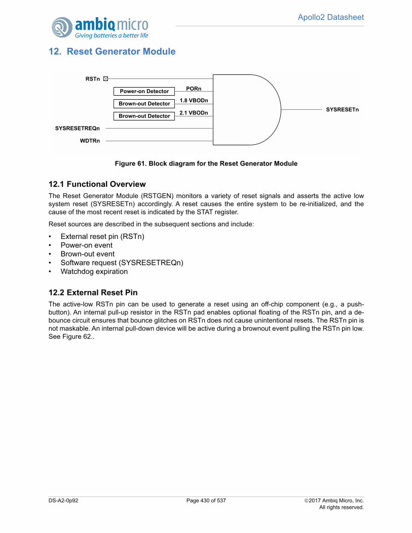
Apollo2 Datasheet
12. Reset Generator Module
Figure 61. Block diagram for the Reset Generator Module
12.1 Functional OverviewThe Reset Generator Module (RSTGEN) monitors a variety of reset signals and asserts the active lowsystem reset (SYSRESETn) accordingly. A reset causes the entire system to be re-initialized, and thecause of the most recent reset is indicated by the STAT register.
Reset sources are described in the subsequent sections and include:
• External reset pin (RSTn)• Power-on event• Brown-out event• Software request (SYSRESETREQn)• Watchdog expiration
12.2 External Reset PinThe active-low RSTn pin can be used to generate a reset using an off-chip component (e.g., a push-button). An internal pull-up resistor in the RSTn pad enables optional floating of the RSTn pin, and a de-bounce circuit ensures that bounce glitches on RSTn does not cause unintentional resets. The RSTn pin isnot maskable. An internal pull-down device will be active during a brownout event pulling the RSTn pin low.See Figure 62..
RSTn
PORn
2.1 VBODn
SYSRESETREQn
WDTRn
SYSRESETn1.8 VBODn
Power-on Detector
Brown-out Detector
Brown-out Detector
DS-A2-0p92 Page 430 of 537 2017 Ambiq Micro, Inc.All rights reserved.

Apollo2 Datasheet
Figure 62. Block diagram of circuitry for Reset pin
12.3 Power-on EventAn integrated power-on detector monitors the supply voltage and keeps SYSRESETn asserted while VDDis below the rising power-on voltage, VPOR+ (1.755 V). When VDD rises above VPOR at initial power on,the reset module will initialize the low power analog circuitry followed by de-assertion of SYSRESETn, andnormal operation proceeds. SYSRESETn is re-asserted as soon as VDD falls below the falling power-onvoltage, VPOR- (1.755 V). The power-on reset signal, PORn, is not maskable.
12.4 Brown-out EventAn integrated brown-out detector monitors the supply voltage and causes an automatic and non-configurable reset when the voltage has fallen below the 1.755 V threshold. An optional reset or interruptcan be enabled when the brown-out detector indicates the supply voltage has fallen below the 2.1 Vthreshold. In the event the supply voltage falls below the 1.755 V threshold, or 2.1 V threshold if enabled,the reset module will initiate a system reset, enabling the RSTn pull-down and driving the reset pin low. A1.755 V or 2.1 V BOD reset will be reflected by the setting of the BORSTAT bit in the RSTGEN's STATRegister after reset.
12.5 Software ResetA reset may be generated via software using the Application Interrupt and Reset Control Register (AIRCR)defined in the Cortex-M4. For additional information on the AIRCR, see the ARM document titled “Cortex-M4 Devices Generic User Guide.” The software reset request is not maskable. A second source for theidentical software reset functionality is made available through the SWPOR register in the RSTGENperipheral module.
Strong Pull
Down
RSTn
RST Button
VDD
RSTGEN
RSTn
brownout_n
RSTn Pad IO
DS-A2-0p92 Page 431 of 537 2017 Ambiq Micro, Inc.All rights reserved.
Apollo2 Datasheet
12.6 Software Power On InitializationThe SWPOI register enables the capability for software to perform a substantial reset that includesreloading the low power analog circuitry trim settings set in the flash information space. These values arenot re-loaded from flash info space for Software Reset or External Reset events.
12.7 Watchdog ExpirationThe Watchdog Timer sub-module generates an interrupt if it has not been properly managed by softwarewithin a pre-defined time. The watchdog reset is maskable.
12.8 RSTGEN RegistersMCU Reset Generator
INSTANCE 0 BASE ADDRESS:0x40000000
12.8.1 Register Memory Map
Table 658: RSTGEN Register Map
Address(s) Register Name Description
0x40000000 CFG Configuration Register
0x40000004 SWPOI Software POI Reset
0x40000008 SWPOR Software POR Reset
0x4000000C STAT Status Register
0x40000010 CLRSTAT Clear the status register
0x40000014 TPIU_RST TPIU reset
0x40000200 INTEN Reset Interrupt register: Enable
0x40000204 INTSTAT Reset Interrupt register: Status
0x40000208 INTCLR Reset Interrupt register: Clear
0x4000020C INTSET Reset Interrupt register: Set
DS-A2-0p92 Page 432 of 537 2017 Ambiq Micro, Inc.All rights reserved.
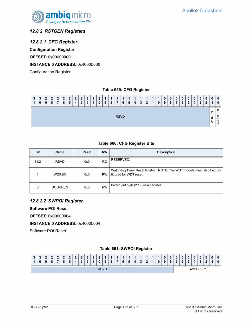
Apollo2 Datasheet
12.8.2 RSTGEN Registers
12.8.2.1 CFG Register
Configuration Register
OFFSET: 0x00000000
INSTANCE 0 ADDRESS: 0x40000000
Configuration Register
12.8.2.2 SWPOI Register
Software POI Reset
OFFSET: 0x00000004
INSTANCE 0 ADDRESS: 0x40000004
Software POI Reset
Table 659: CFG Register
31
30
29
28
27
26
25
24
23
22
21
20
19
18
17
16
15
14
13
12
11
10
09
08
07
06
05
04
03
02
01
00
RSVD
WD
RE
N
BO
DH
RE
N
Table 660: CFG Register Bits
Bit Name Reset RW Description
31:2 RSVD 0x0 RORESERVED.
1 WDREN 0x0 RWWatchdog Timer Reset Enable. NOTE: The WDT module must also be con-figured for WDT reset.
0 BODHREN 0x0 RWBrown out high (2.1v) reset enable.
Table 661: SWPOI Register
31
30
29
28
27
26
25
24
23
22
21
20
19
18
17
16
15
14
13
12
11
10
09
08
07
06
05
04
03
02
01
00
RSVD SWPOIKEY
DS-A2-0p92 Page 433 of 537 2017 Ambiq Micro, Inc.All rights reserved.
Apollo2 Datasheet
12.8.2.3 SWPOR Register
Software POR Reset
OFFSET: 0x00000008
INSTANCE 0 ADDRESS: 0x40000008
Software POR Reset
12.8.2.4 STAT Register
Status Register
OFFSET: 0x0000000C
INSTANCE 0 ADDRESS: 0x4000000C
Status Register
Table 662: SWPOI Register Bits
Bit Name Reset RW Description
31:8 RSVD 0x0 RORESERVED.
7:0 SWPOIKEY 0x0 WO
0x1B generates a software POI reset.
KEYVALUE = 0x1B - Writing 0x1B key value generates a software POIreset.
Table 663: SWPOR Register
31
30
29
28
27
26
25
24
23
22
21
20
19
18
17
16
15
14
13
12
11
10
09
08
07
06
05
04
03
02
01
00
RSVD SWPORKEY
Table 664: SWPOR Register Bits
Bit Name Reset RW Description
31:8 RSVD 0x0 RORESERVED.
7:0 SWPORKEY 0x0 WO
0xD4 generates a software POR reset.
KEYVALUE = 0xD4 - Writing 0xD4 key value generates a software PORreset.
DS-A2-0p92 Page 434 of 537 2017 Ambiq Micro, Inc.All rights reserved.

Apollo2 Datasheet
12.8.2.5 CLRSTAT Register
Clear the status register
OFFSET: 0x00000010
INSTANCE 0 ADDRESS: 0x40000010
Clear the status register
Table 665: STAT Register
31
30
29
28
27
26
25
24
23
22
21
20
19
18
17
16
15
14
13
12
11
10
09
08
07
06
05
04
03
02
01
00
RSVD
WD
RS
TAT
DB
GR
STA
T
PO
IRS
TAT
SW
RS
TAT
BO
RS
TAT
PO
RS
TAT
EX
RS
TAT
Table 666: STAT Register Bits
Bit Name Reset RW Description
31:7 RSVD 0x0 RORESERVED.
6 WDRSTAT 0x0 ROReset was initiated by a Watchdog Timer Reset.
5 DBGRSTAT 0x0 ROReset was a initiated by Debugger Reset.
4 POIRSTAT 0x0 ROReset was a initiated by Software POI Reset.
3 SWRSTAT 0x0 ROReset was a initiated by SW POR or AIRCR Reset.
2 BORSTAT 0x0 ROReset was initiated by a Brown-Out Reset.
1 PORSTAT 0x0 ROReset was initiated by a Power-On Reset.
0 EXRSTAT 0x0 ROReset was initiated by an External Reset.
Table 667: CLRSTAT Register
31
30
29
28
27
26
25
24
23
22
21
20
19
18
17
16
15
14
13
12
11
10
09
08
07
06
05
04
03
02
01
00
RSVD
CLR
STA
T
DS-A2-0p92 Page 435 of 537 2017 Ambiq Micro, Inc.All rights reserved.
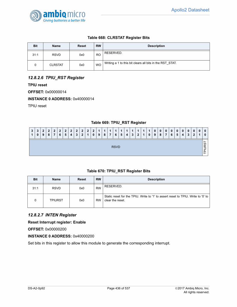
Apollo2 Datasheet
12.8.2.6 TPIU_RST Register
TPIU reset
OFFSET: 0x00000014
INSTANCE 0 ADDRESS: 0x40000014
TPIU reset
12.8.2.7 INTEN Register
Reset Interrupt register: Enable
OFFSET: 0x00000200
INSTANCE 0 ADDRESS: 0x40000200
Set bits in this register to allow this module to generate the corresponding interrupt.
Table 668: CLRSTAT Register Bits
Bit Name Reset RW Description
31:1 RSVD 0x0 RORESERVED.
0 CLRSTAT 0x0 WOWriting a 1 to this bit clears all bits in the RST_STAT.
Table 669: TPIU_RST Register
31
30
29
28
27
26
25
24
23
22
21
20
19
18
17
16
15
14
13
12
11
10
09
08
07
06
05
04
03
02
01
00
RSVD
TP
IUR
ST
Table 670: TPIU_RST Register Bits
Bit Name Reset RW Description
31:1 RSVD 0x0 RWRESERVED.
0 TPIURST 0x0 RWStatic reset for the TPIU. Write to '1' to assert reset to TPIU. Write to '0' toclear the reset.
DS-A2-0p92 Page 436 of 537 2017 Ambiq Micro, Inc.All rights reserved.
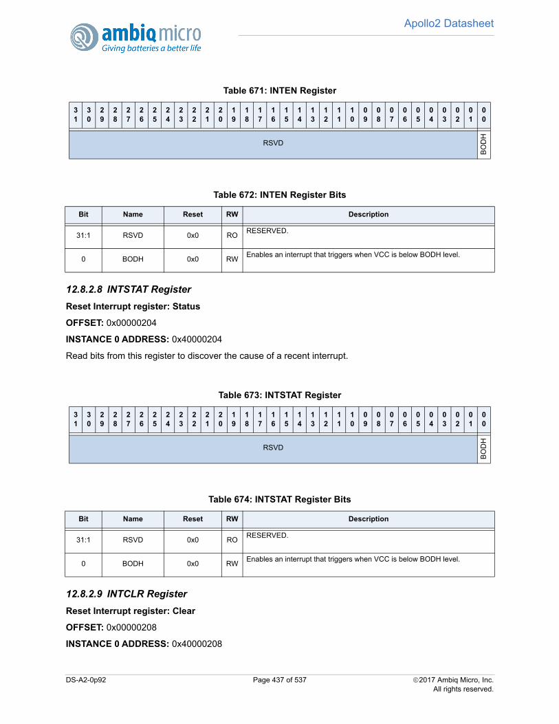
Apollo2 Datasheet
12.8.2.8 INTSTAT Register
Reset Interrupt register: Status
OFFSET: 0x00000204
INSTANCE 0 ADDRESS: 0x40000204
Read bits from this register to discover the cause of a recent interrupt.
12.8.2.9 INTCLR Register
Reset Interrupt register: Clear
OFFSET: 0x00000208
INSTANCE 0 ADDRESS: 0x40000208
Table 671: INTEN Register
31
30
29
28
27
26
25
24
23
22
21
20
19
18
17
16
15
14
13
12
11
10
09
08
07
06
05
04
03
02
01
00
RSVD
BO
DH
Table 672: INTEN Register Bits
Bit Name Reset RW Description
31:1 RSVD 0x0 RORESERVED.
0 BODH 0x0 RWEnables an interrupt that triggers when VCC is below BODH level.
Table 673: INTSTAT Register
31
30
29
28
27
26
25
24
23
22
21
20
19
18
17
16
15
14
13
12
11
10
09
08
07
06
05
04
03
02
01
00
RSVD
BO
DH
Table 674: INTSTAT Register Bits
Bit Name Reset RW Description
31:1 RSVD 0x0 RORESERVED.
0 BODH 0x0 RWEnables an interrupt that triggers when VCC is below BODH level.
DS-A2-0p92 Page 437 of 537 2017 Ambiq Micro, Inc.All rights reserved.

Apollo2 Datasheet
Write a 1 to a bit in this register to clear the interrupt status associated with that bit.
12.8.2.10INTSET Register
Reset Interrupt register: Set
OFFSET: 0x0000020C
INSTANCE 0 ADDRESS: 0x4000020C
Write a 1 to a bit in this register to instantly generate an interrupt from this module. (Generally used fortesting purposes).
Table 675: INTCLR Register
31
30
29
28
27
26
25
24
23
22
21
20
19
18
17
16
15
14
13
12
11
10
09
08
07
06
05
04
03
02
01
00
RSVD
BO
DH
Table 676: INTCLR Register Bits
Bit Name Reset RW Description
31:1 RSVD 0x0 RORESERVED.
0 BODH 0x0 RWEnables an interrupt that triggers when VCC is below BODH level.
Table 677: INTSET Register
31
30
29
28
27
26
25
24
23
22
21
20
19
18
17
16
15
14
13
12
11
10
09
08
07
06
05
04
03
02
01
00
RSVDB
OD
H
Table 678: INTSET Register Bits
Bit Name Reset RW Description
31:1 RSVD 0x0 RORESERVED.
0 BODH 0x0 RWEnables an interrupt that triggers when VCC is below BODH level.
DS-A2-0p92 Page 438 of 537 2017 Ambiq Micro, Inc.All rights reserved.

Apollo2 Datasheet
13. UART Module
Figure 63. Block Diagram for the UART Module
13.1 FeaturesThe UART Module includes the following key features:
• Operates independently, allowing the MCU to enter a low power sleep mode during communication• 32 x 8 transmit FIFO and 32 x 12 receive FIFO to reduce MCU computational load• Programmable baud rate generator capable of a maximum rate of 921,600 bits per second• Fully programmable data size, parity, and stop bit length• Programmable hardware flow control• Support for full-duplex and half-duplex communication• Loopback functionality for diagnostics and testing
13.2 Functional OverviewShown in Figure 63, the UART Module converts parallel data written through the APB Slave port into serialdata which is transmitted to an external device. It also receives serial data from an external device andconverts it to parallel data, which is then stored in a buffer until the CPU reads the data.
The UART Module includes a programmable baud rate generator which is capable of operating at amaximum of 921,600 bits per second. An interrupt generator will optionally send interrupts to the CPU corefor transmit, receive and error events.
Internally, the UART Module maintains two FIFOs. The transmit FIFO is 1-byte wide with 32 locations. Thereceive FIFO is 12-bits wide with 32 locations. The extra four bits in the receive FIFO are used to captureany error status information that the MCU needs to analyze.
APB
UART TX
UART RX
IRQ
APB Slave
Transmit FIFO
Register Block
Receive FIFO
Interrupt Generation
Transmit Interface
Receive Interface
DS-A2-0p92 Page 439 of 537 2017 Ambiq Micro, Inc.All rights reserved.
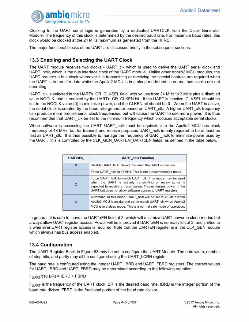
Apollo2 Datasheet
Clocking to the UART serial logic is generated by a dedicated UARTCLK from the Clock GeneratorModule. The frequency of this clock is determined by the desired baud rate. For maximum baud rates, thisclock would be clocked at the 24 MHz maximum as generated from the HFRC.
The major functional blocks of the UART are discussed briefly in the subsequent sections.
13.3 Enabling and Selecting the UART ClockThe UART module receives two clocks - UART_clk which is used to derive the UART serial clock andUART_hclk, which is the bus interface clock of the UART module. Unlike other Apollo2 MCU modules, theUART requires a bus clock whenever it is transmitting or receiving, so special controls are required whenthe UART is to transfer data while the Apollo2 MCU is in a sleep mode and its normal bus clocks are notoperating.
UART_clk is selected in the UARTx_CR_CLKSEL field, with values from 24 MHz to 3 MHz plus a disabledvalue NOCLK, and is enabled by the UARTx_CR_CLKEN bit. If the UART is inactive, CLKSEL should beset to the NOCLK value (0) to minimize power, and the CLKEN bit should be 0. When the UART is active,the serial clock is created by the baud rate generator based on UART_clk. A higher UART_clk frequencycan produce more precise serial clock frequencies, but will cause the UART to use more power. It is thusrecommended that UART_clk be set to the minimum frequency which produces acceptable serial clocks.
When software is accessing the UART, UART_hclk must be equivalent to the Apollo2 MCU bus clockfrequency of 48 MHz, but for transmit and receive purposes UART_hclk is only required to be at least asfast as UART_clk. It is thus possible to manage the frequency of UART_hclk to minimize power used bythe UART. This is controlled by the CLK_GEN_UARTEN_UARTxEN fields, as defined in the table below.
In general, it is safe to leave the UARTxEN field at 3, which will minimize UART power in sleep modes butalways allow UART register access. Power will be improved if UARTxEN is normally left at 2, and shifted to3 whenever UART register access is required. Note that the UARTEN register is in the CLK_GEN modulewhich always has bus access enabled.
13.4 ConfigurationThe UART Register Block in Figure 63 may be set to configure the UART Module. The data width, numberof stop bits, and parity may all be configured using the UART_LCRH register.
The baud rate is configured using the integer UART_IBRD and UART_FBRD registers. The correct valuesfor UART_IBRD and UART_FBRD may be determined according to the following equation:
FUART/(16·BR) = IBRD + FBRD
FUART is the frequency of the UART clock. BR is the desired baud rate. IBRD is the integer portion of thebaud rate divisor. FBRD is the fractional portion of the baud rate divisor.
UARTxEN UART_hclk Function
0 Disable UART_hclk. Select this when the UART is inactive.
1 Force UART_hclk to 48MHz. This is not a recommended mode.
2
Force UART_hclk to match UART_clk. This mode may be usedwhen the UART is actively transmitting or receiving, or isexpected to receive a transmission. This minimizes power in theUART but does not allow software access to UART registers.
3
Automatic. In this mode, UART_hclk will be set to 48 MHz when
Apollo2 MCU is awake and set to match UART_clk when Apollo2
MCU is in a sleep mode. This is a normal safe mode of operation.
DS-A2-0p92 Page 440 of 537 2017 Ambiq Micro, Inc.All rights reserved.
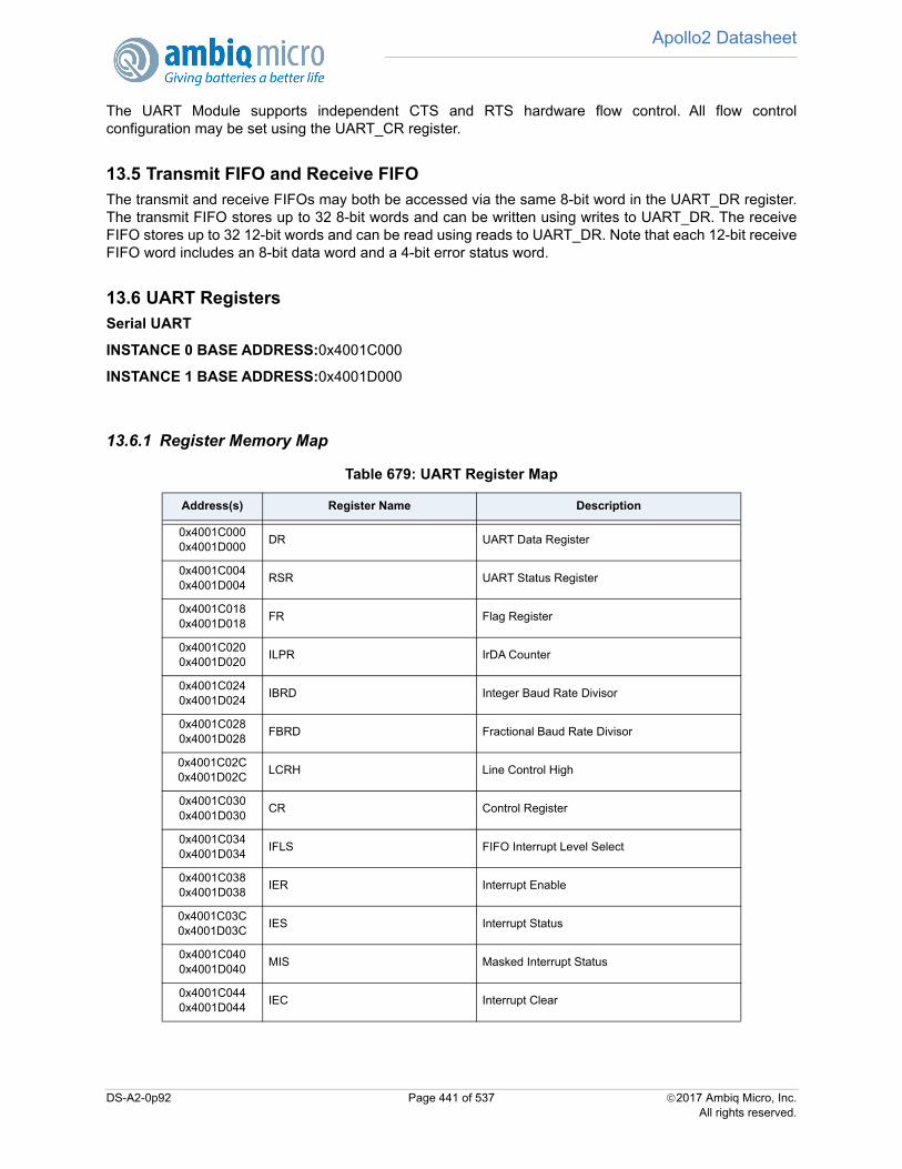
Apollo2 Datasheet
The UART Module supports independent CTS and RTS hardware flow control. All flow controlconfiguration may be set using the UART_CR register.
13.5 Transmit FIFO and Receive FIFOThe transmit and receive FIFOs may both be accessed via the same 8-bit word in the UART_DR register.The transmit FIFO stores up to 32 8-bit words and can be written using writes to UART_DR. The receiveFIFO stores up to 32 12-bit words and can be read using reads to UART_DR. Note that each 12-bit receiveFIFO word includes an 8-bit data word and a 4-bit error status word.
13.6 UART RegistersSerial UART
INSTANCE 0 BASE ADDRESS:0x4001C000
INSTANCE 1 BASE ADDRESS:0x4001D000
13.6.1 Register Memory Map
Table 679: UART Register Map
Address(s) Register Name Description
0x4001C0000x4001D000
DR UART Data Register
0x4001C0040x4001D004
RSR UART Status Register
0x4001C0180x4001D018
FR Flag Register
0x4001C0200x4001D020
ILPR IrDA Counter
0x4001C0240x4001D024
IBRD Integer Baud Rate Divisor
0x4001C0280x4001D028
FBRD Fractional Baud Rate Divisor
0x4001C02C0x4001D02C
LCRH Line Control High
0x4001C0300x4001D030
CR Control Register
0x4001C0340x4001D034
IFLS FIFO Interrupt Level Select
0x4001C0380x4001D038
IER Interrupt Enable
0x4001C03C0x4001D03C
IES Interrupt Status
0x4001C0400x4001D040
MIS Masked Interrupt Status
0x4001C0440x4001D044
IEC Interrupt Clear
DS-A2-0p92 Page 441 of 537 2017 Ambiq Micro, Inc.All rights reserved.
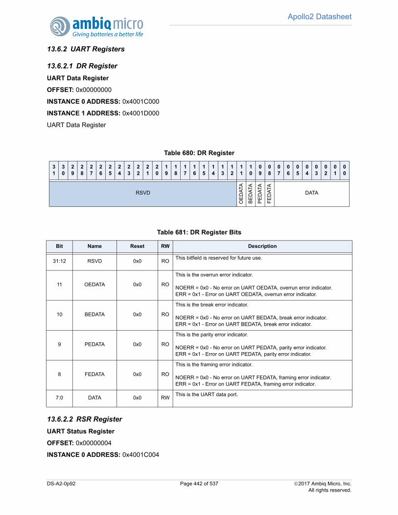
Apollo2 Datasheet
13.6.2 UART Registers
13.6.2.1 DR Register
UART Data Register
OFFSET: 0x00000000
INSTANCE 0 ADDRESS: 0x4001C000
INSTANCE 1 ADDRESS: 0x4001D000
UART Data Register
13.6.2.2 RSR Register
UART Status Register
OFFSET: 0x00000004
INSTANCE 0 ADDRESS: 0x4001C004
Table 680: DR Register
31
30
29
28
27
26
25
24
23
22
21
20
19
18
17
16
15
14
13
12
11
10
09
08
07
06
05
04
03
02
01
00
RSVD
OE
DA
TA
BE
DA
TA
PE
DA
TA
FE
DA
TA
DATA
Table 681: DR Register Bits
Bit Name Reset RW Description
31:12 RSVD 0x0 ROThis bitfield is reserved for future use.
11 OEDATA 0x0 RO
This is the overrun error indicator.
NOERR = 0x0 - No error on UART OEDATA, overrun error indicator.ERR = 0x1 - Error on UART OEDATA, overrun error indicator.
10 BEDATA 0x0 RO
This is the break error indicator.
NOERR = 0x0 - No error on UART BEDATA, break error indicator.ERR = 0x1 - Error on UART BEDATA, break error indicator.
9 PEDATA 0x0 RO
This is the parity error indicator.
NOERR = 0x0 - No error on UART PEDATA, parity error indicator.ERR = 0x1 - Error on UART PEDATA, parity error indicator.
8 FEDATA 0x0 RO
This is the framing error indicator.
NOERR = 0x0 - No error on UART FEDATA, framing error indicator.ERR = 0x1 - Error on UART FEDATA, framing error indicator.
7:0 DATA 0x0 RWThis is the UART data port.
DS-A2-0p92 Page 442 of 537 2017 Ambiq Micro, Inc.All rights reserved.

Apollo2 Datasheet
INSTANCE 1 ADDRESS: 0x4001D004
UART Status Register
13.6.2.3 FR Register
Flag Register
OFFSET: 0x00000018
INSTANCE 0 ADDRESS: 0x4001C018
INSTANCE 1 ADDRESS: 0x4001D018
Flag Register
Table 682: RSR Register
31
30
29
28
27
26
25
24
23
22
21
20
19
18
17
16
15
14
13
12
11
10
09
08
07
06
05
04
03
02
01
00
RSVD
OE
STA
T
BE
STA
T
PE
STA
T
FE
STA
T
Table 683: RSR Register Bits
Bit Name Reset RW Description
31:4 RSVD 0x0 ROThis bitfield is reserved for future use.
3 OESTAT 0x0 RW
This is the overrun error indicator.
NOERR = 0x0 - No error on UART OESTAT, overrun error indicator.ERR = 0x1 - Error on UART OESTAT, overrun error indicator.
2 BESTAT 0x0 RW
This is the break error indicator.
NOERR = 0x0 - No error on UART BESTAT, break error indicator.ERR = 0x1 - Error on UART BESTAT, break error indicator.
1 PESTAT 0x0 RW
This is the parity error indicator.
NOERR = 0x0 - No error on UART PESTAT, parity error indicator.ERR = 0x1 - Error on UART PESTAT, parity error indicator.
0 FESTAT 0x0 RW
This is the framing error indicator.
NOERR = 0x0 - No error on UART FESTAT, framing error indicator.ERR = 0x1 - Error on UART FESTAT, framing error indicator.
DS-A2-0p92 Page 443 of 537 2017 Ambiq Micro, Inc.All rights reserved.
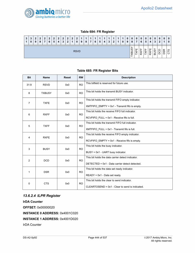
Apollo2 Datasheet
13.6.2.4 ILPR Register
IrDA Counter
OFFSET: 0x00000020
INSTANCE 0 ADDRESS: 0x4001C020
INSTANCE 1 ADDRESS: 0x4001D020
IrDA Counter
Table 684: FR Register
31
30
29
28
27
26
25
24
23
22
21
20
19
18
17
16
15
14
13
12
11
10
09
08
07
06
05
04
03
02
01
00
RSVD
TX
BU
SY
TX
FE
RX
FF
TX
FF
RX
FE
BU
SY
DC
D
DS
R
CT
S
Table 685: FR Register Bits
Bit Name Reset RW Description
31:9 RSVD 0x0 ROThis bitfield is reserved for future use.
8 TXBUSY 0x0 ROThis bit holds the transmit BUSY indicator.
7 TXFE 0x0 ROThis bit holds the transmit FIFO empty indicator.
XMTFIFO_EMPTY = 0x1 - Transmit fifo is empty.
6 RXFF 0x0 ROThis bit holds the receive FIFO full indicator.
RCVFIFO_FULL = 0x1 - Receive fifo is full.
5 TXFF 0x0 ROThis bit holds the transmit FIFO full indicator.
XMTFIFO_FULL = 0x1 - Transmit fifo is full.
4 RXFE 0x0 ROThis bit holds the receive FIFO empty indicator.
RCVFIFO_EMPTY = 0x1 - Receive fifo is empty.
3 BUSY 0x0 ROThis bit holds the busy indicator.
BUSY = 0x1 - UART busy indicator.
2 DCD 0x0 ROThis bit holds the data carrier detect indicator.
DETECTED = 0x1 - Data carrier detect detected.
1 DSR 0x0 ROThis bit holds the data set ready indicator.
READY = 0x1 - Data set ready.
0 CTS 0x0 ROThis bit holds the clear to send indicator.
CLEARTOSEND = 0x1 - Clear to send is indicated.
DS-A2-0p92 Page 444 of 537 2017 Ambiq Micro, Inc.All rights reserved.
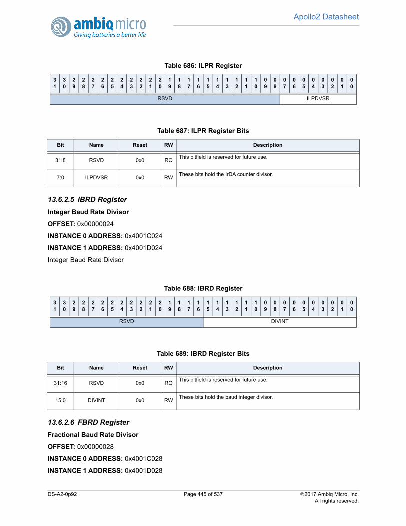
Apollo2 Datasheet
13.6.2.5 IBRD Register
Integer Baud Rate Divisor
OFFSET: 0x00000024
INSTANCE 0 ADDRESS: 0x4001C024
INSTANCE 1 ADDRESS: 0x4001D024
Integer Baud Rate Divisor
13.6.2.6 FBRD Register
Fractional Baud Rate Divisor
OFFSET: 0x00000028
INSTANCE 0 ADDRESS: 0x4001C028
INSTANCE 1 ADDRESS: 0x4001D028
Table 686: ILPR Register
31
30
29
28
27
26
25
24
23
22
21
20
19
18
17
16
15
14
13
12
11
10
09
08
07
06
05
04
03
02
01
00
RSVD ILPDVSR
Table 687: ILPR Register Bits
Bit Name Reset RW Description
31:8 RSVD 0x0 ROThis bitfield is reserved for future use.
7:0 ILPDVSR 0x0 RWThese bits hold the IrDA counter divisor.
Table 688: IBRD Register
31
30
29
28
27
26
25
24
23
22
21
20
19
18
17
16
15
14
13
12
11
10
09
08
07
06
05
04
03
02
01
00
RSVD DIVINT
Table 689: IBRD Register Bits
Bit Name Reset RW Description
31:16 RSVD 0x0 ROThis bitfield is reserved for future use.
15:0 DIVINT 0x0 RWThese bits hold the baud integer divisor.
DS-A2-0p92 Page 445 of 537 2017 Ambiq Micro, Inc.All rights reserved.
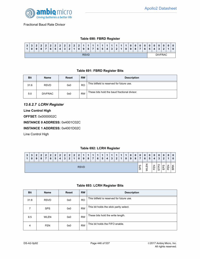
Apollo2 Datasheet
Fractional Baud Rate Divisor
13.6.2.7 LCRH Register
Line Control High
OFFSET: 0x0000002C
INSTANCE 0 ADDRESS: 0x4001C02C
INSTANCE 1 ADDRESS: 0x4001D02C
Line Control High
Table 690: FBRD Register
31
30
29
28
27
26
25
24
23
22
21
20
19
18
17
16
15
14
13
12
11
10
09
08
07
06
05
04
03
02
01
00
RSVD DIVFRAC
Table 691: FBRD Register Bits
Bit Name Reset RW Description
31:6 RSVD 0x0 ROThis bitfield is reserved for future use.
5:0 DIVFRAC 0x0 RWThese bits hold the baud fractional divisor.
Table 692: LCRH Register
31
30
29
28
27
26
25
24
23
22
21
20
19
18
17
16
15
14
13
12
11
10
09
08
07
06
05
04
03
02
01
00
RSVD
SP
S
WL
EN
FE
N
ST
P2
EP
S
PE
N
BR
K
Table 693: LCRH Register Bits
Bit Name Reset RW Description
31:8 RSVD 0x0 ROThis bitfield is reserved for future use.
7 SPS 0x0 RWThis bit holds the stick parity select.
6:5 WLEN 0x0 RWThese bits hold the write length.
4 FEN 0x0 RWThis bit holds the FIFO enable.
DS-A2-0p92 Page 446 of 537 2017 Ambiq Micro, Inc.All rights reserved.

Apollo2 Datasheet
13.6.2.8 CR Register
Control Register
OFFSET: 0x00000030
INSTANCE 0 ADDRESS: 0x4001C030
INSTANCE 1 ADDRESS: 0x4001D030
Control Register
3 STP2 0x0 RWThis bit holds the two stop bits select.
2 EPS 0x0 RWThis bit holds the even parity select.
1 PEN 0x0 RWThis bit holds the parity enable.
0 BRK 0x0 RWThis bit holds the break set.
Table 694: CR Register
31
30
29
28
27
26
25
24
23
22
21
20
19
18
17
16
15
14
13
12
11
10
09
08
07
06
05
04
03
02
01
00
RSVD
CT
SE
N
RT
SE
N
OU
T2
OU
T1
RT
S
DT
R
RX
E
TX
E
LBE
CLK
SE
L
CLK
EN
SIR
LP
SIR
EN
UA
RT
EN
Table 695: CR Register Bits
Bit Name Reset RW Description
31:16 RSVD 0x0 ROThis bitfield is reserved for future use.
15 CTSEN 0x0 RWThis bit enables CTS hardware flow control.
14 RTSEN 0x0 RWThis bit enables RTS hardware flow control.
13 OUT2 0x0 RWThis bit holds modem Out2.
12 OUT1 0x0 RWThis bit holds modem Out1.
11 RTS 0x0 RWThis bit enables request to send.
10 DTR 0x0 RWThis bit enables data transmit ready.
Table 693: LCRH Register Bits
Bit Name Reset RW Description
DS-A2-0p92 Page 447 of 537 2017 Ambiq Micro, Inc.All rights reserved.
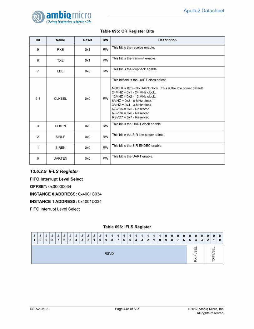
Apollo2 Datasheet
13.6.2.9 IFLS Register
FIFO Interrupt Level Select
OFFSET: 0x00000034
INSTANCE 0 ADDRESS: 0x4001C034
INSTANCE 1 ADDRESS: 0x4001D034
FIFO Interrupt Level Select
9 RXE 0x1 RWThis bit is the receive enable.
8 TXE 0x1 RWThis bit is the transmit enable.
7 LBE 0x0 RWThis bit is the loopback enable.
6:4 CLKSEL 0x0 RW
This bitfield is the UART clock select.
NOCLK = 0x0 - No UART clock. This is the low power default.24MHZ = 0x1 - 24 MHz clock.12MHZ = 0x2 - 12 MHz clock.6MHZ = 0x3 - 6 MHz clock.3MHZ = 0x4 - 3 MHz clock.RSVD5 = 0x5 - Reserved.RSVD6 = 0x6 - Reserved.RSVD7 = 0x7 - Reserved.
3 CLKEN 0x0 RWThis bit is the UART clock enable.
2 SIRLP 0x0 RWThis bit is the SIR low power select.
1 SIREN 0x0 RWThis bit is the SIR ENDEC enable.
0 UARTEN 0x0 RWThis bit is the UART enable.
Table 696: IFLS Register
31
30
29
28
27
26
25
24
23
22
21
20
19
18
17
16
15
14
13
12
11
10
09
08
07
06
05
04
03
02
01
00
RSVD
RX
IFLS
EL
TX
IFLS
EL
Table 695: CR Register Bits
Bit Name Reset RW Description
DS-A2-0p92 Page 448 of 537 2017 Ambiq Micro, Inc.All rights reserved.
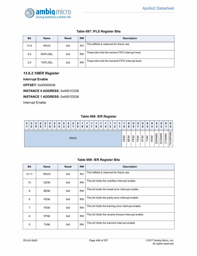
Apollo2 Datasheet
13.6.2.10IER Register
Interrupt Enable
OFFSET: 0x00000038
INSTANCE 0 ADDRESS: 0x4001C038
INSTANCE 1 ADDRESS: 0x4001D038
Interrupt Enable
Table 697: IFLS Register Bits
Bit Name Reset RW Description
31:6 RSVD 0x0 ROThis bitfield is reserved for future use.
5:3 RXIFLSEL 0x2 RWThese bits hold the receive FIFO interrupt level.
2:0 TXIFLSEL 0x2 RWThese bits hold the transmit FIFO interrupt level.
Table 698: IER Register
31
30
29
28
27
26
25
24
23
22
21
20
19
18
17
16
15
14
13
12
11
10
09
08
07
06
05
04
03
02
01
00
RSVD
OE
IM
BE
IM
PE
IM
FE
IM
RT
IM
TX
IM
RX
IM
DS
RM
IM
DC
DM
IM
CT
SM
IM
TX
CM
PM
IM
Table 699: IER Register Bits
Bit Name Reset RW Description
31:11 RSVD 0x0 ROThis bitfield is reserved for future use.
10 OEIM 0x0 RWThis bit holds the overflow interrupt enable.
9 BEIM 0x0 RWThis bit holds the break error interrupt enable.
8 PEIM 0x0 RWThis bit holds the parity error interrupt enable.
7 FEIM 0x0 RWThis bit holds the framing error interrupt enable.
6 RTIM 0x0 RWThis bit holds the receive timeout interrupt enable.
5 TXIM 0x0 RWThis bit holds the transmit interrupt enable.
DS-A2-0p92 Page 449 of 537 2017 Ambiq Micro, Inc.All rights reserved.
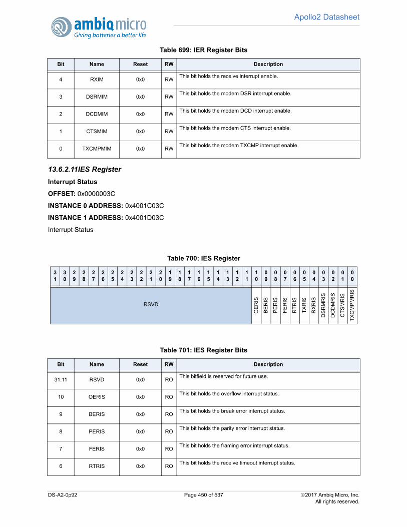
Apollo2 Datasheet
13.6.2.11IES Register
Interrupt Status
OFFSET: 0x0000003C
INSTANCE 0 ADDRESS: 0x4001C03C
INSTANCE 1 ADDRESS: 0x4001D03C
Interrupt Status
4 RXIM 0x0 RWThis bit holds the receive interrupt enable.
3 DSRMIM 0x0 RWThis bit holds the modem DSR interrupt enable.
2 DCDMIM 0x0 RWThis bit holds the modem DCD interrupt enable.
1 CTSMIM 0x0 RWThis bit holds the modem CTS interrupt enable.
0 TXCMPMIM 0x0 RWThis bit holds the modem TXCMP interrupt enable.
Table 700: IES Register
31
30
29
28
27
26
25
24
23
22
21
20
19
18
17
16
15
14
13
12
11
10
09
08
07
06
05
04
03
02
01
00
RSVD
OE
RIS
BE
RIS
PE
RIS
FE
RIS
RT
RIS
TX
RIS
RX
RIS
DS
RM
RIS
DC
DM
RIS
CT
SM
RIS
TX
CM
PM
RIS
Table 701: IES Register Bits
Bit Name Reset RW Description
31:11 RSVD 0x0 ROThis bitfield is reserved for future use.
10 OERIS 0x0 ROThis bit holds the overflow interrupt status.
9 BERIS 0x0 ROThis bit holds the break error interrupt status.
8 PERIS 0x0 ROThis bit holds the parity error interrupt status.
7 FERIS 0x0 ROThis bit holds the framing error interrupt status.
6 RTRIS 0x0 ROThis bit holds the receive timeout interrupt status.
Table 699: IER Register Bits
Bit Name Reset RW Description
DS-A2-0p92 Page 450 of 537 2017 Ambiq Micro, Inc.All rights reserved.
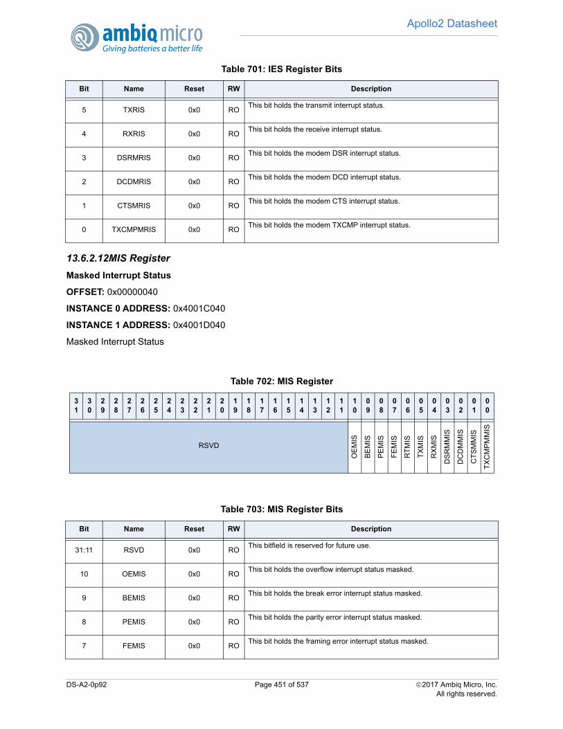
Apollo2 Datasheet
13.6.2.12MIS Register
Masked Interrupt Status
OFFSET: 0x00000040
INSTANCE 0 ADDRESS: 0x4001C040
INSTANCE 1 ADDRESS: 0x4001D040
Masked Interrupt Status
5 TXRIS 0x0 ROThis bit holds the transmit interrupt status.
4 RXRIS 0x0 ROThis bit holds the receive interrupt status.
3 DSRMRIS 0x0 ROThis bit holds the modem DSR interrupt status.
2 DCDMRIS 0x0 ROThis bit holds the modem DCD interrupt status.
1 CTSMRIS 0x0 ROThis bit holds the modem CTS interrupt status.
0 TXCMPMRIS 0x0 ROThis bit holds the modem TXCMP interrupt status.
Table 702: MIS Register
31
30
29
28
27
26
25
24
23
22
21
20
19
18
17
16
15
14
13
12
11
10
09
08
07
06
05
04
03
02
01
00
RSVD
OE
MIS
BE
MIS
PE
MIS
FE
MIS
RT
MIS
TX
MIS
RX
MIS
DS
RM
MIS
DC
DM
MIS
CT
SM
MIS
TX
CM
PM
MIS
Table 703: MIS Register Bits
Bit Name Reset RW Description
31:11 RSVD 0x0 ROThis bitfield is reserved for future use.
10 OEMIS 0x0 ROThis bit holds the overflow interrupt status masked.
9 BEMIS 0x0 ROThis bit holds the break error interrupt status masked.
8 PEMIS 0x0 ROThis bit holds the parity error interrupt status masked.
7 FEMIS 0x0 ROThis bit holds the framing error interrupt status masked.
Table 701: IES Register Bits
Bit Name Reset RW Description
DS-A2-0p92 Page 451 of 537 2017 Ambiq Micro, Inc.All rights reserved.
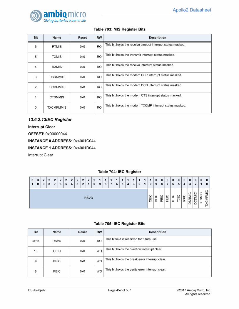
Apollo2 Datasheet
13.6.2.13IEC Register
Interrupt Clear
OFFSET: 0x00000044
INSTANCE 0 ADDRESS: 0x4001C044
INSTANCE 1 ADDRESS: 0x4001D044
Interrupt Clear
6 RTMIS 0x0 ROThis bit holds the receive timeout interrupt status masked.
5 TXMIS 0x0 ROThis bit holds the transmit interrupt status masked.
4 RXMIS 0x0 ROThis bit holds the receive interrupt status masked.
3 DSRMMIS 0x0 ROThis bit holds the modem DSR interrupt status masked.
2 DCDMMIS 0x0 ROThis bit holds the modem DCD interrupt status masked.
1 CTSMMIS 0x0 ROThis bit holds the modem CTS interrupt status masked.
0 TXCMPMMIS 0x0 ROThis bit holds the modem TXCMP interrupt status masked.
Table 704: IEC Register
31
30
29
28
27
26
25
24
23
22
21
20
19
18
17
16
15
14
13
12
11
10
09
08
07
06
05
04
03
02
01
00
RSVD
OE
IC
BE
IC
PE
IC
FE
IC
RT
IC
TX
IC
RX
IC
DS
RM
IC
DC
DM
IC
CT
SM
IC
TX
CM
PM
IC
Table 705: IEC Register Bits
Bit Name Reset RW Description
31:11 RSVD 0x0 ROThis bitfield is reserved for future use.
10 OEIC 0x0 WOThis bit holds the overflow interrupt clear.
9 BEIC 0x0 WOThis bit holds the break error interrupt clear.
8 PEIC 0x0 WOThis bit holds the parity error interrupt clear.
Table 703: MIS Register Bits
Bit Name Reset RW Description
DS-A2-0p92 Page 452 of 537 2017 Ambiq Micro, Inc.All rights reserved.
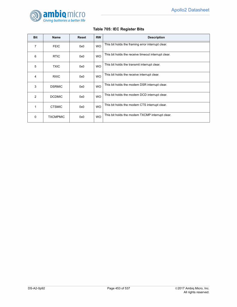
Apollo2 Datasheet
7 FEIC 0x0 WOThis bit holds the framing error interrupt clear.
6 RTIC 0x0 WOThis bit holds the receive timeout interrupt clear.
5 TXIC 0x0 WOThis bit holds the transmit interrupt clear.
4 RXIC 0x0 WOThis bit holds the receive interrupt clear.
3 DSRMIC 0x0 WOThis bit holds the modem DSR interrupt clear.
2 DCDMIC 0x0 WOThis bit holds the modem DCD interrupt clear.
1 CTSMIC 0x0 WOThis bit holds the modem CTS interrupt clear.
0 TXCMPMIC 0x0 WOThis bit holds the modem TXCMP interrupt clear.
Table 705: IEC Register Bits
Bit Name Reset RW Description
DS-A2-0p92 Page 453 of 537 2017 Ambiq Micro, Inc.All rights reserved.
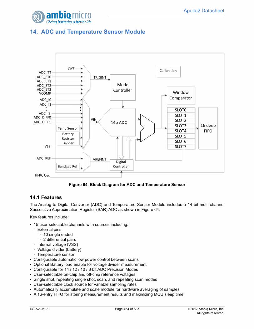
Apollo2 Datasheet
14. ADC and Temperature Sensor Module
Figure 64. Block Diagram for ADC and Temperature Sensor
14.1 FeaturesThe Analog to Digital Converter (ADC) and Temperature Sensor Module includes a 14 bit multi-channelSuccessive Approximation Register (SAR) ADC as shown in Figure 64.
Key features include:
15 user-selectable channels with sources including:- External pins
- 10 single ended- 2 differential pairs
- Internal voltage (VSS)- Voltage divider (battery)- Temperature sensor
Configurable automatic low power control between scans Optional Battery load enable for voltage divider measurement Configurable for 14 / 12 / 10 / 8 bit ADC Precision Modes User-selectable on-chip and off-chip reference voltages Single shot, repeating single shot, scan, and repeating scan modes User-selectable clock source for variable sampling rates Automatically accumulate and scale module for hardware averaging of samples A 16-entry FIFO for storing measurement results and maximizing MCU sleep time
SLOT0
14b ADC
ADC_I0ADC_I1
SWT
...
ADC_TTADC_ET0ADC_ET1
Mode Controller
VREFINTADC_REF
Bandgap Ref
ADC_I9
VSS
ADC_ET3Window
Comparator
...
Temp Sensor
TRIGINT
VIN
HFRC Osc
Digital Controller
SLOT1SLOT2SLOT3SLOT4SLOT5SLOT6SLOT7
16 deep FIFO
Calibration
Battery Resistor Divider
ADC_ET2
ADC_DIFF0ADC_DIFF1
VCOMP
DS-A2-0p92 Page 454 of 537 2017 Ambiq Micro, Inc.All rights reserved.
Apollo2 Datasheet
Window comparator for monitoring voltages excursions into or out of user-selectable thresholds Up to 2.67 MS/s effective continuous, multi-slot sampling rate Interrupts for FIFO full, FIFO almost full, Scan Complete, Conversion Complete, Window Incursion Win-
dow Excursion
14.2 Functional OverviewThe Apollo2 MCU integrates a sophisticated 14 bit successive approximation Analog to Digital Converter(ADC) block for sensing both internal and external voltages. The block provides eight separately managedconversion requests, called slots. The result of each conversion requests is delivered to a 16 deep FIFO.Firmware can utilize various interrupt notifications to determine when to collect the sampled data from theFIFO. This block is extremely effective at automatically managing its power states and its clock sources.
14.2.1 Clock Source and Dividers
The ADC runs off of the HFRC clock source. When the ADC block is enabled and has an active scan inprogress, it requests an HFRC clock source. There is an automatic hardware hand shake between theclock generator and the ADC. If the ADC is the only block requesting an HFRC based clock, then theHFRC will be automatically started. The ADC can be configured to completely power down the HFRCbetween scans if the startup latency is acceptable or it can leave the HFRC powered on between scans ifTHE application requires low latency between successive conversions. The ADC supports 2 clockfrequency modes: 24MHz and 48MHz HFRC. 48MHz mode is the default mode of operation.
14.2.2 15 Channel Analog Mux
As shown in Figure 64, the ADC block contains a 15 channel analog multiplexer on the input port to theanalog to digital converter. Twelve (12) of the GPIO pins on the Apollo2 MCU can be selected as analoginputs to the ADC through a combination of settings in the PAD configuration registers in the GPIO blockand settings in the configuration registers described below.
The analog mux channels are connected as follows:
1. ADC_EXT0 external GPIO pin connection.
2. ADC_EXT1 external GPIO pin connection.
3. ADC_EXT2 external GPIO pin connection.
4. ADC_EXT3 external GPIO pin connection.
5. ADC_EXT4 external GPIO pin connection.
6. ADC_EXT5 external GPIO pin connection.
7. ADC_EXT6 external GPIO pin connection.
8. ADC_EXT7 external GPIO pin connection.
9. ADC_EXT8 external GPIO pin connection.
10. ADC_EXT9 external GPIO pin connection.
11. ADC_EXT_DIFF0P external GPIO connection (muxed with EXT8)
ADC_EXT_DIFF0N external GPIO connection (muxed with EXT9)
12. ADC_EXT6 ADC_EXT DIFF1N external GPIO pin connection.
ADC_EXT7 ADC_EXTDIFF1P external GPIO pin connection.
13. ADC_TEMP internal temperature sensor.
14. ADC_DIV3 internal voltage divide by 3 connection to the input power rail.
15. ADC_VSS internal ground connection.
DS-A2-0p92 Page 455 of 537 2017 Ambiq Micro, Inc.All rights reserved.
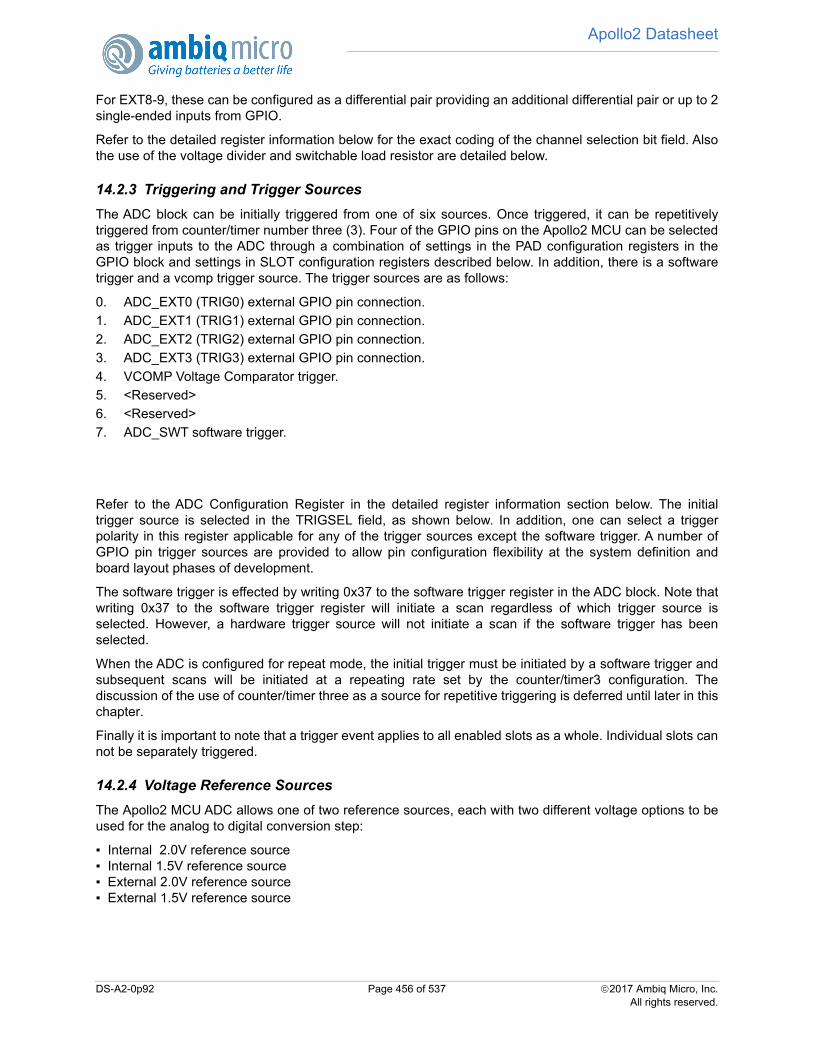
Apollo2 Datasheet
For EXT8-9, these can be configured as a differential pair providing an additional differential pair or up to 2single-ended inputs from GPIO.
Refer to the detailed register information below for the exact coding of the channel selection bit field. Alsothe use of the voltage divider and switchable load resistor are detailed below.
14.2.3 Triggering and Trigger Sources
The ADC block can be initially triggered from one of six sources. Once triggered, it can be repetitivelytriggered from counter/timer number three (3). Four of the GPIO pins on the Apollo2 MCU can be selectedas trigger inputs to the ADC through a combination of settings in the PAD configuration registers in theGPIO block and settings in SLOT configuration registers described below. In addition, there is a softwaretrigger and a vcomp trigger source. The trigger sources are as follows:
0. ADC_EXT0 (TRIG0) external GPIO pin connection.
1. ADC_EXT1 (TRIG1) external GPIO pin connection.
2. ADC_EXT2 (TRIG2) external GPIO pin connection.
3. ADC_EXT3 (TRIG3) external GPIO pin connection.
4. VCOMP Voltage Comparator trigger.
5. <Reserved>
6. <Reserved>
7. ADC_SWT software trigger.
Refer to the ADC Configuration Register in the detailed register information section below. The initialtrigger source is selected in the TRIGSEL field, as shown below. In addition, one can select a triggerpolarity in this register applicable for any of the trigger sources except the software trigger. A number ofGPIO pin trigger sources are provided to allow pin configuration flexibility at the system definition andboard layout phases of development.
The software trigger is effected by writing 0x37 to the software trigger register in the ADC block. Note thatwriting 0x37 to the software trigger register will initiate a scan regardless of which trigger source isselected. However, a hardware trigger source will not initiate a scan if the software trigger has beenselected.
When the ADC is configured for repeat mode, the initial trigger must be initiated by a software trigger andsubsequent scans will be initiated at a repeating rate set by the counter/timer3 configuration. Thediscussion of the use of counter/timer three as a source for repetitive triggering is deferred until later in thischapter.
Finally it is important to note that a trigger event applies to all enabled slots as a whole. Individual slots cannot be separately triggered.
14.2.4 Voltage Reference Sources
The Apollo2 MCU ADC allows one of two reference sources, each with two different voltage options to beused for the analog to digital conversion step:
Internal 2.0V reference source Internal 1.5V reference source External 2.0V reference source External 1.5V reference source
DS-A2-0p92 Page 456 of 537 2017 Ambiq Micro, Inc.All rights reserved.

Apollo2 Datasheet
14.2.5 Eight Automatically Managed Conversion Slots
The ADC block contains eight conversion slot control registers, one for each of the eight slots. These canbe thought of as time slots in the conversion process. When a slot is enabled, it participates in aconversion cycle. The ADC’s mode controller cycles through up to eight time slots each time it is triggered.For each slot that is enabled, a conversion cycle is performed based on the settings in the slotconfiguration register for that slot. Slots are enabled when the LSB of the slot configuration is set to one. See “One SLOT Configuration Register” on page 457.
The window comparator enable will be discussed in a subsequent section, below. See “WindowComparator” on page 461. The number of samples to accumulate will also be explained in a subsequentsection. See “Automatic Sample Accumulation and Scaling” on page 457.
As described above, the channel select bit field specifies which one of the analog multiplexer channels willbe used for the conversions requested for an individual slot. See “15 Channel Analog Mux” on page 455.
Each of the eight conversion slots can independently specify:
Analog Multiplexer Channel Selection Participation in Window Comparisons Automatic Sample Accumulation
14.2.6 Automatic Sample Accumulation and Scaling
The ADC block offers a facility for the automatic accumulation of samples without requiring coreinvolvement. Thus up to 128 samples per slot can be accumulated without waking the core. This facilitatesaveraging algorithms to smooth out the data samples. Each slot can request from 1 to 128 samples to beaccumulated before producing a result in the FIFO. NOTE: each slot can independently specify how manysamples to accumulate so results can enter the FIFO from different slots at different rates.
All slots write their accumulated results to the FIFO in exactly the same format regardless of how manysamples were accumulated to produce the results. shows the format that is used by all conversions. Thisis a scaled integer format with a 6-bit fractional part. The precision mode for each determines the format forthe FIFO data. 14-bit, 12-bit, 10-bit and 8-bit precision modes respectively correspond to 14.6, 12.6, 10.6and 8.6 formats.
IMPORTANT: if the accumulation control for a slot is set for one sample with 14-bit precision, then the 14-bit value coming from the ADC will be inserted into bits 6 through 19 in this format and the lower 6 bits arezero'd. If the accumulation control for a slot is set for two samples with 8-bit precision, then the 8-bitaverage integer value will be placed in bits 6 through 13, the 1 bit fractional number is placed in bit 5 andthe lower 5 fractional bits are zero'd..
Table 706: One SLOT Configuration Register
31
30
29
28
27
26
25
24
23
22
21
20
19
18
17
16
15
14
13
12
11
10
09
08
07
06
05
04
03
02
01
00
Reserved
#Samples
to Accum.
ReservedCHANNEL SELECT
Reserved
WIN
DO
W_C
OM
P
SLO
T_E
NA
BLE
DS-A2-0p92 Page 457 of 537 2017 Ambiq Micro, Inc.All rights reserved.
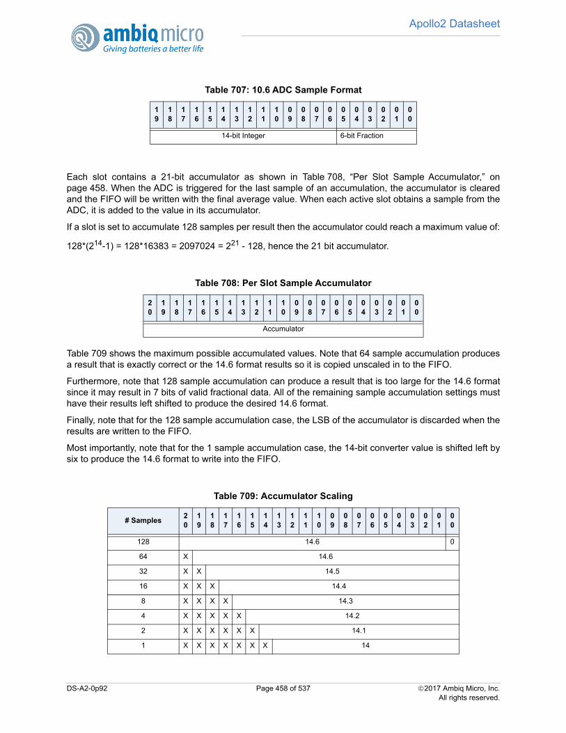
Apollo2 Datasheet
Each slot contains a 21-bit accumulator as shown in Table 708, “Per Slot Sample Accumulator,” onpage 458. When the ADC is triggered for the last sample of an accumulation, the accumulator is clearedand the FIFO will be written with the final average value. When each active slot obtains a sample from theADC, it is added to the value in its accumulator.
If a slot is set to accumulate 128 samples per result then the accumulator could reach a maximum value of:
128*(214-1) = 128*16383 = 2097024 = 221 - 128, hence the 21 bit accumulator.
Table 709 shows the maximum possible accumulated values. Note that 64 sample accumulation producesa result that is exactly correct or the 14.6 format results so it is copied unscaled in to the FIFO.
Furthermore, note that 128 sample accumulation can produce a result that is too large for the 14.6 formatsince it may result in 7 bits of valid fractional data. All of the remaining sample accumulation settings musthave their results left shifted to produce the desired 14.6 format.
Finally, note that for the 128 sample accumulation case, the LSB of the accumulator is discarded when theresults are written to the FIFO.
Most importantly, note that for the 1 sample accumulation case, the 14-bit converter value is shifted left bysix to produce the 14.6 format to write into the FIFO.
Table 707: 10.6 ADC Sample Format
19
18
17
16
15
14
13
12
11
10
09
08
07
06
05
04
03
02
01
00
14-bit Integer 6-bit Fraction
Table 708: Per Slot Sample Accumulator
20
19
18
17
16
15
14
13
12
11
10
09
08
07
06
05
04
03
02
01
00
Accumulator
Table 709: Accumulator Scaling
# Samples20
19
18
17
16
15
14
13
12
11
10
09
08
07
06
05
04
03
02
01
00
128 14.6 0
64 X 14.6
32 X X 14.5
16 X X X 14.4
8 X X X X 14.3
4 X X X X X 14.2
2 X X X X X X 14.1
1 X X X X X X X 14
DS-A2-0p92 Page 458 of 537 2017 Ambiq Micro, Inc.All rights reserved.
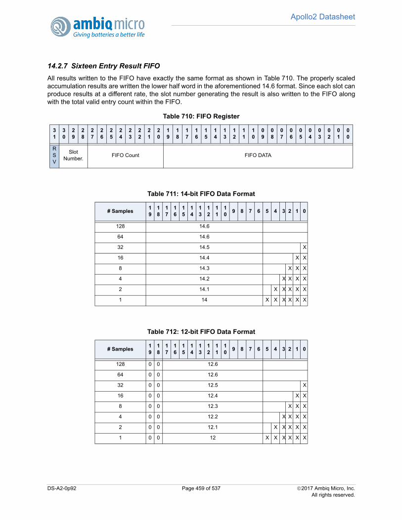
Apollo2 Datasheet
14.2.7 Sixteen Entry Result FIFO
All results written to the FIFO have exactly the same format as shown in Table 710. The properly scaledaccumulation results are written the lower half word in the aforementioned 14.6 format. Since each slot canproduce results at a different rate, the slot number generating the result is also written to the FIFO alongwith the total valid entry count within the FIFO.
Table 710: FIFO Register
31
30
29
28
27
26
25
24
23
22
21
20
19
18
17
16
15
14
13
12
11
10
09
08
07
06
05
04
03
02
01
00
RSV
Slot Number.
FIFO Count FIFO DATA
Table 711: 14-bit FIFO Data Format
# Samples19
18
17
16
15
14
13
12
11
10
9 8 7 6 5 4 3 2 1 0
128 14.6
64 14.6
32 14.5 X
16 14.4 X X
8 14.3 X X X
4 14.2 X X X X
2 14.1 X X X X X
1 14 X X X X X X
Table 712: 12-bit FIFO Data Format
# Samples19
18
17
16
15
14
13
12
11
10
9 8 7 6 5 4 3 2 1 0
128 0 0 12.6
64 0 0 12.6
32 0 0 12.5 X
16 0 0 12.4 X X
8 0 0 12.3 X X X
4 0 0 12.2 X X X X
2 0 0 12.1 X X X X X
1 0 0 12 X X X X X X
DS-A2-0p92 Page 459 of 537 2017 Ambiq Micro, Inc.All rights reserved.
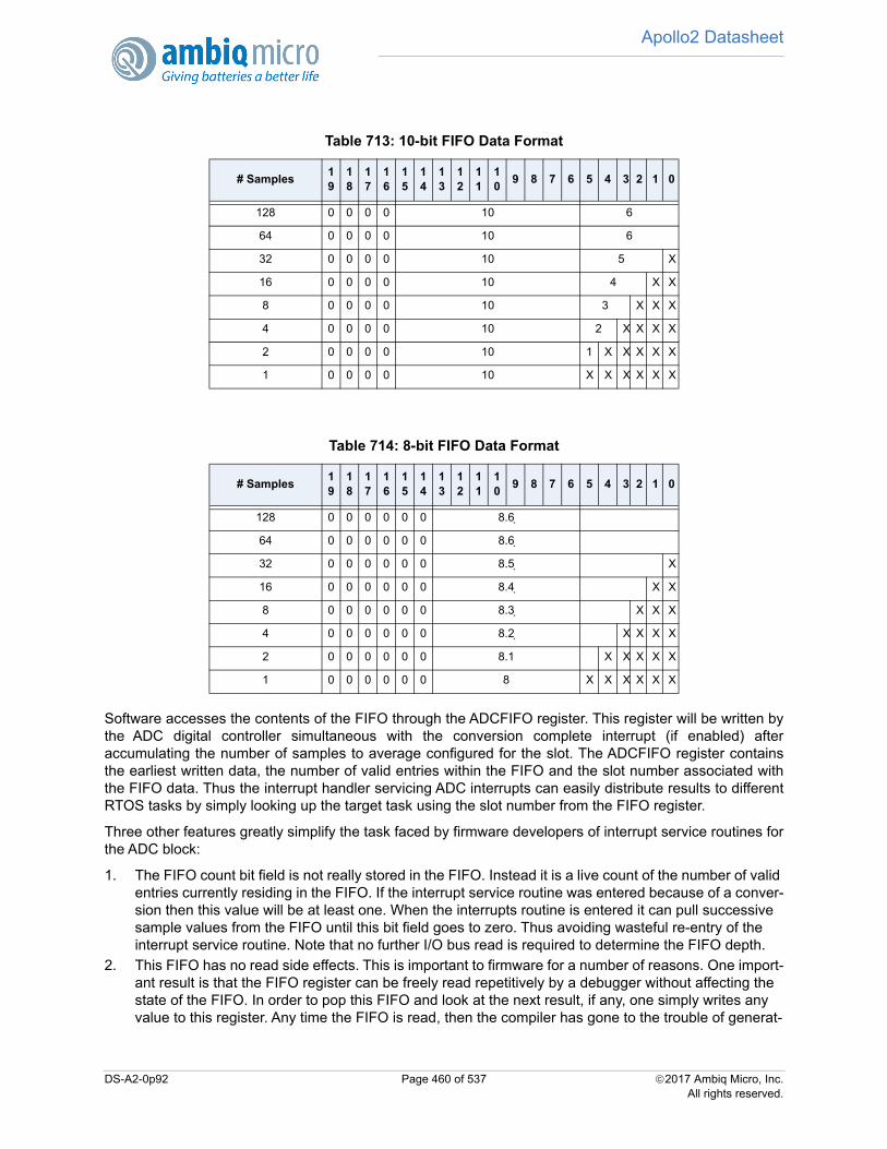
Apollo2 Datasheet
Software accesses the contents of the FIFO through the ADCFIFO register. This register will be written bythe ADC digital controller simultaneous with the conversion complete interrupt (if enabled) afteraccumulating the number of samples to average configured for the slot. The ADCFIFO register containsthe earliest written data, the number of valid entries within the FIFO and the slot number associated withthe FIFO data. Thus the interrupt handler servicing ADC interrupts can easily distribute results to differentRTOS tasks by simply looking up the target task using the slot number from the FIFO register.
Three other features greatly simplify the task faced by firmware developers of interrupt service routines forthe ADC block:
1. The FIFO count bit field is not really stored in the FIFO. Instead it is a live count of the number of valid entries currently residing in the FIFO. If the interrupt service routine was entered because of a conver-sion then this value will be at least one. When the interrupts routine is entered it can pull successive sample values from the FIFO until this bit field goes to zero. Thus avoiding wasteful re-entry of the interrupt service routine. Note that no further I/O bus read is required to determine the FIFO depth.
2. This FIFO has no read side effects. This is important to firmware for a number of reasons. One import-ant result is that the FIFO register can be freely read repetitively by a debugger without affecting the state of the FIFO. In order to pop this FIFO and look at the next result, if any, one simply writes any value to this register. Any time the FIFO is read, then the compiler has gone to the trouble of generat-
Table 713: 10-bit FIFO Data Format
# Samples19
18
17
16
15
14
13
12
11
10
9 8 7 6 5 4 3 2 1 0
128 0 0 0 0 10 6
64 0 0 0 0 10 6
32 0 0 0 0 10 5 X
16 0 0 0 0 10 4 X X
8 0 0 0 0 10 3 X X X
4 0 0 0 0 10 2 X X X X
2 0 0 0 0 10 1 X X X X X
1 0 0 0 0 10 X X X X X X
Table 714: 8-bit FIFO Data Format
# Samples19
18
17
16
15
14
13
12
11
10
9 8 7 6 5 4 3 2 1 0
128 0 0 0 0 0 0 8.6
64 0 0 0 0 0 0 8.6
32 0 0 0 0 0 0 8.5 X
16 0 0 0 0 0 0 8.4 X X
8 0 0 0 0 0 0 8.3 X X X
4 0 0 0 0 0 0 8.2 X X X X
2 0 0 0 0 0 0 8.1 X X X X X
1 0 0 0 0 0 0 8 X X X X X X
DS-A2-0p92 Page 460 of 537 2017 Ambiq Micro, Inc.All rights reserved.
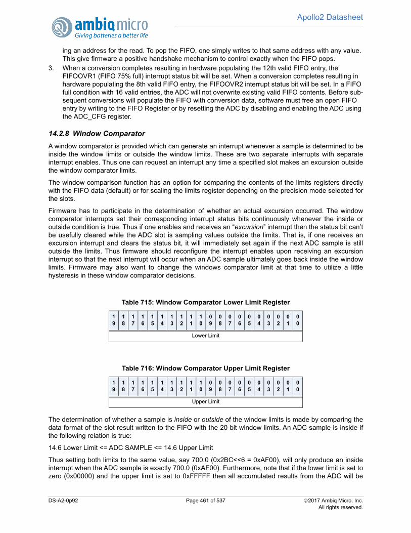
Apollo2 Datasheet
ing an address for the read. To pop the FIFO, one simply writes to that same address with any value. This give firmware a positive handshake mechanism to control exactly when the FIFO pops.
3. When a conversion completes resulting in hardware populating the 12th valid FIFO entry, the FIFOOVR1 (FIFO 75% full) interrupt status bit will be set. When a conversion completes resulting in hardware populating the 8th valid FIFO entry, the FIFOOVR2 interrupt status bit will be set. In a FIFO full condition with 16 valid entries, the ADC will not overwrite existing valid FIFO contents. Before sub-sequent conversions will populate the FIFO with conversion data, software must free an open FIFO entry by writing to the FIFO Register or by resetting the ADC by disabling and enabling the ADC using the ADC_CFG register.
14.2.8 Window Comparator
A window comparator is provided which can generate an interrupt whenever a sample is determined to beinside the window limits or outside the window limits. These are two separate interrupts with separateinterrupt enables. Thus one can request an interrupt any time a specified slot makes an excursion outsidethe window comparator limits.
The window comparison function has an option for comparing the contents of the limits registers directlywith the FIFO data (default) or for scaling the limits register depending on the precision mode selected forthe slots.
Firmware has to participate in the determination of whether an actual excursion occurred. The windowcomparator interrupts set their corresponding interrupt status bits continuously whenever the inside oroutside condition is true. Thus if one enables and receives an “excursion” interrupt then the status bit can’tbe usefully cleared while the ADC slot is sampling values outside the limits. That is, if one receives anexcursion interrupt and clears the status bit, it will immediately set again if the next ADC sample is stilloutside the limits. Thus firmware should reconfigure the interrupt enables upon receiving an excursioninterrupt so that the next interrupt will occur when an ADC sample ultimately goes back inside the windowlimits. Firmware may also want to change the windows comparator limit at that time to utilize a littlehysteresis in these window comparator decisions.
The determination of whether a sample is inside or outside of the window limits is made by comparing thedata format of the slot result written to the FIFO with the 20 bit window limits. An ADC sample is inside ifthe following relation is true:
14.6 Lower Limit <= ADC SAMPLE <= 14.6 Upper Limit
Thus setting both limits to the same value, say 700.0 (0x2BC<<6 = 0xAF00), will only produce an insideinterrupt when the ADC sample is exactly 700.0 (0xAF00). Furthermore, note that if the lower limit is set tozero (0x00000) and the upper limit is set to 0xFFFFF then all accumulated results from the ADC will be
Table 715: Window Comparator Lower Limit Register
19
18
17
16
15
14
13
12
11
10
09
08
07
06
05
04
03
02
01
00
Lower Limit
Table 716: Window Comparator Upper Limit Register
19
18
17
16
15
14
13
12
11
10
09
08
07
06
05
04
03
02
01
00
Upper Limit
DS-A2-0p92 Page 461 of 537 2017 Ambiq Micro, Inc.All rights reserved.
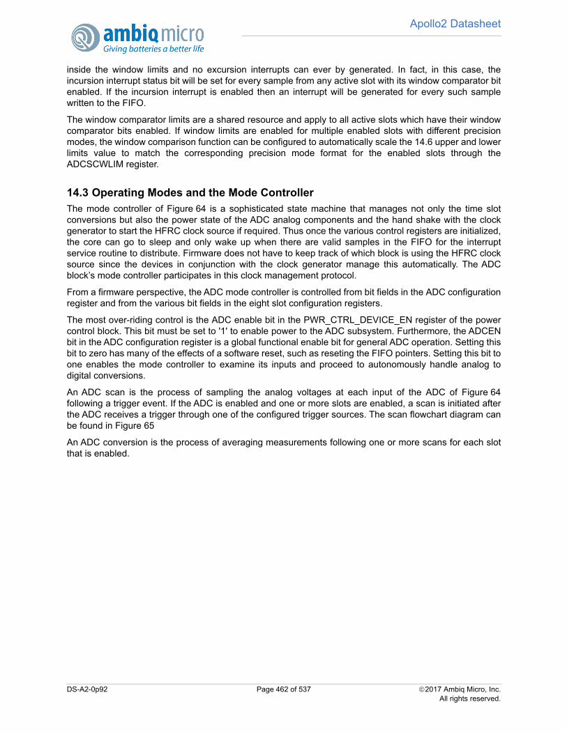
Apollo2 Datasheet
inside the window limits and no excursion interrupts can ever by generated. In fact, in this case, theincursion interrupt status bit will be set for every sample from any active slot with its window comparator bitenabled. If the incursion interrupt is enabled then an interrupt will be generated for every such samplewritten to the FIFO.
The window comparator limits are a shared resource and apply to all active slots which have their windowcomparator bits enabled. If window limits are enabled for multiple enabled slots with different precisionmodes, the window comparison function can be configured to automatically scale the 14.6 upper and lowerlimits value to match the corresponding precision mode format for the enabled slots through theADCSCWLIM register.
14.3 Operating Modes and the Mode ControllerThe mode controller of Figure 64 is a sophisticated state machine that manages not only the time slotconversions but also the power state of the ADC analog components and the hand shake with the clockgenerator to start the HFRC clock source if required. Thus once the various control registers are initialized,the core can go to sleep and only wake up when there are valid samples in the FIFO for the interruptservice routine to distribute. Firmware does not have to keep track of which block is using the HFRC clocksource since the devices in conjunction with the clock generator manage this automatically. The ADCblock’s mode controller participates in this clock management protocol.
From a firmware perspective, the ADC mode controller is controlled from bit fields in the ADC configurationregister and from the various bit fields in the eight slot configuration registers.
The most over-riding control is the ADC enable bit in the PWR_CTRL_DEVICE_EN register of the powercontrol block. This bit must be set to '1' to enable power to the ADC subsystem. Furthermore, the ADCENbit in the ADC configuration register is a global functional enable bit for general ADC operation. Setting thisbit to zero has many of the effects of a software reset, such as reseting the FIFO pointers. Setting this bit toone enables the mode controller to examine its inputs and proceed to autonomously handle analog todigital conversions.
An ADC scan is the process of sampling the analog voltages at each input of the ADC of Figure 64following a trigger event. If the ADC is enabled and one or more slots are enabled, a scan is initiated afterthe ADC receives a trigger through one of the configured trigger sources. The scan flowchart diagram canbe found in Figure 65
An ADC conversion is the process of averaging measurements following one or more scans for each slotthat is enabled.
DS-A2-0p92 Page 462 of 537 2017 Ambiq Micro, Inc.All rights reserved.
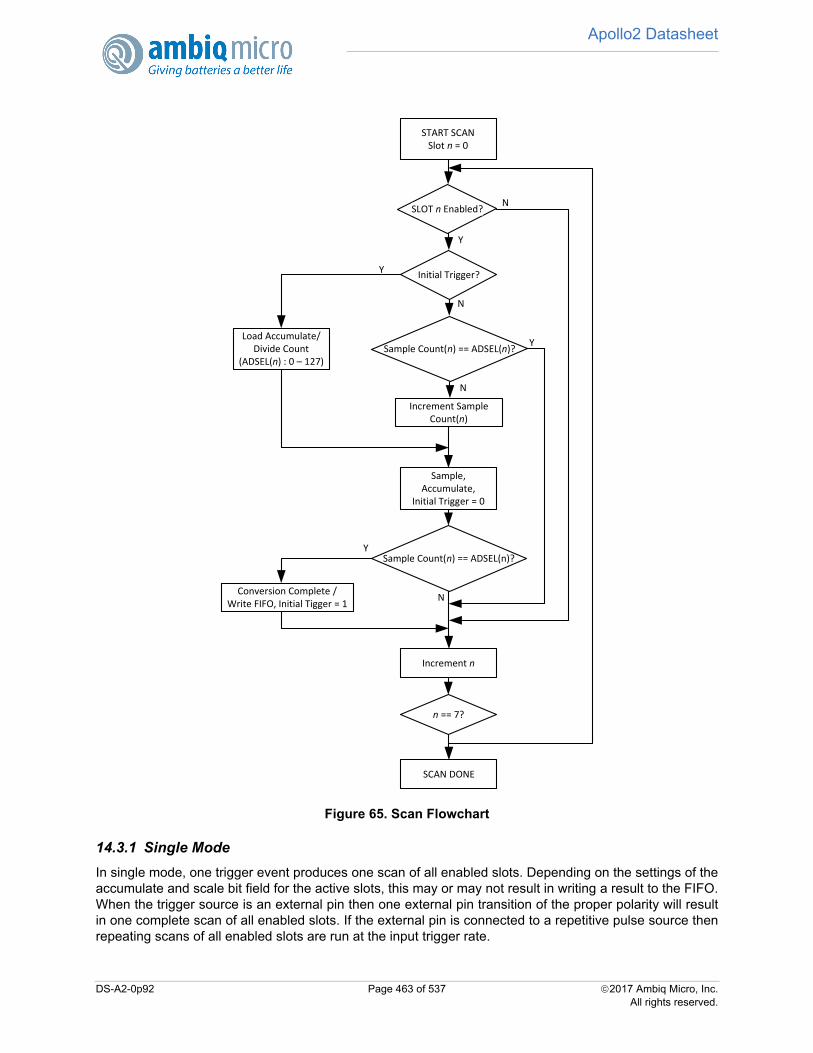
Apollo2 Datasheet
Figure 65. Scan Flowchart
14.3.1 Single Mode
In single mode, one trigger event produces one scan of all enabled slots. Depending on the settings of theaccumulate and scale bit field for the active slots, this may or may not result in writing a result to the FIFO.When the trigger source is an external pin then one external pin transition of the proper polarity will resultin one complete scan of all enabled slots. If the external pin is connected to a repetitive pulse source thenrepeating scans of all enabled slots are run at the input trigger rate.
START SCANSlot n = 0
SLOT n Enabled?
Load Accumulate/Divide Count
(ADSEL(n) : 0 – 127)
Y
N
Y
Increment Sample Count(n)
Sample,Accumulate,
Initial Trigger = 0
N
Sample Count(n) == ADSEL(n)?
Conversion Complete / Write FIFO, Initial Tigger = 1
Increment n
n == 7?
Initial Trigger?
SCAN DONE
N
N
Y
YSample Count(n) == ADSEL(n)?
DS-A2-0p92 Page 463 of 537 2017 Ambiq Micro, Inc.All rights reserved.
Apollo2 Datasheet
14.3.2 Repeat Mode
Counter/Timer 3A has a bit in its configuration register that allows it to be a source of repetitive triggers forthe ADC. If counter/timer 3 is initialized for this purpose then one only needs to turn on the RPTEN bit inthe ADC configuration registers to enable this mode in the ADC.
NOTE: the mode controller does not process these repetitive triggers from the counter/timer until a firsttriggering event occurs from the normal trigger sources. Thus one can select software triggering in theTRIGSEL field and set up all of the other ADC registers for the desired sample acquisitions. Then one canwrite to the software trigger register and the mode controller will enter REPEAT mode. In repeat mode, themode controller waits only for each successive counter/timer 3A input to launch a scan of all enabled slots.
14.3.3 Low Power Modes
An application may use the ADC in one of three power modes. Each mode has different implications fromoverall energy perspective relative to the startup latency from trigger-to-data as well as the standby powerconsumed. The table below is intended to provide guidance on which mode may be more effective basedon latency tolerance. This table should only be used as a reference.
14.3.3.1 Low Power Mode 0
Low Power Mode 0 (LPMODE0) enables the lowest latency from trigger to conversion data available. Thismode leaves the reference buffer powered on between scans to bypass any startup latency between
triggers1.
14.3.3.2 Low Power Mode 1
Low power mode 1 (LPMODE1) is a power mode whereby the ADC Digital Controller will automaticallypower off the ADC clocks, analog ADC and reference buffer between scans while maintaining ADCcalibration data. This mode may operate autonomously without CPU interaction, even while the CPU is insleep or deepsleep mode for repeat mode triggers or hardware triggers. While operating in this mode, theADC Digital Controller may be used to burst through multiple scans enabling max sample rate datacollection if the triggers are running at a rate at least 2x the maximum sample rate until the final scan hascompleted. When a scan completes without a pending trigger latched, the ADC subsystem will enter a lowpower state until the next trigger event.
14.3.3.3 Low Power Mode 2
If desirable, for applications requiring infrequent conversions, software may choose to operate the ADC inLPMODE2, whereby the full ADC Analog and Digital subsystem remains completely powered off between
Table 717: ADC Power Modes
LPMODE Definition Entry Latency
0ADC is kept active continuously (used in continu-ous sampling scenarios)
0 (requires initial
calibration)
1
ADC is mostly powered off between samples,HFRC is duty cycled between samples. No cali-bration required after initial calibration)
<50μs(shorter for lower
resolution)
2
ADC is completely powered off between sam-ples, HFRC is duty cycled between samples.Requires recalibration for each conversion.
<600μs
1. The reference buffer will not be powered on when the ADC is configured for external reference
DS-A2-0p92 Page 464 of 537 2017 Ambiq Micro, Inc.All rights reserved.
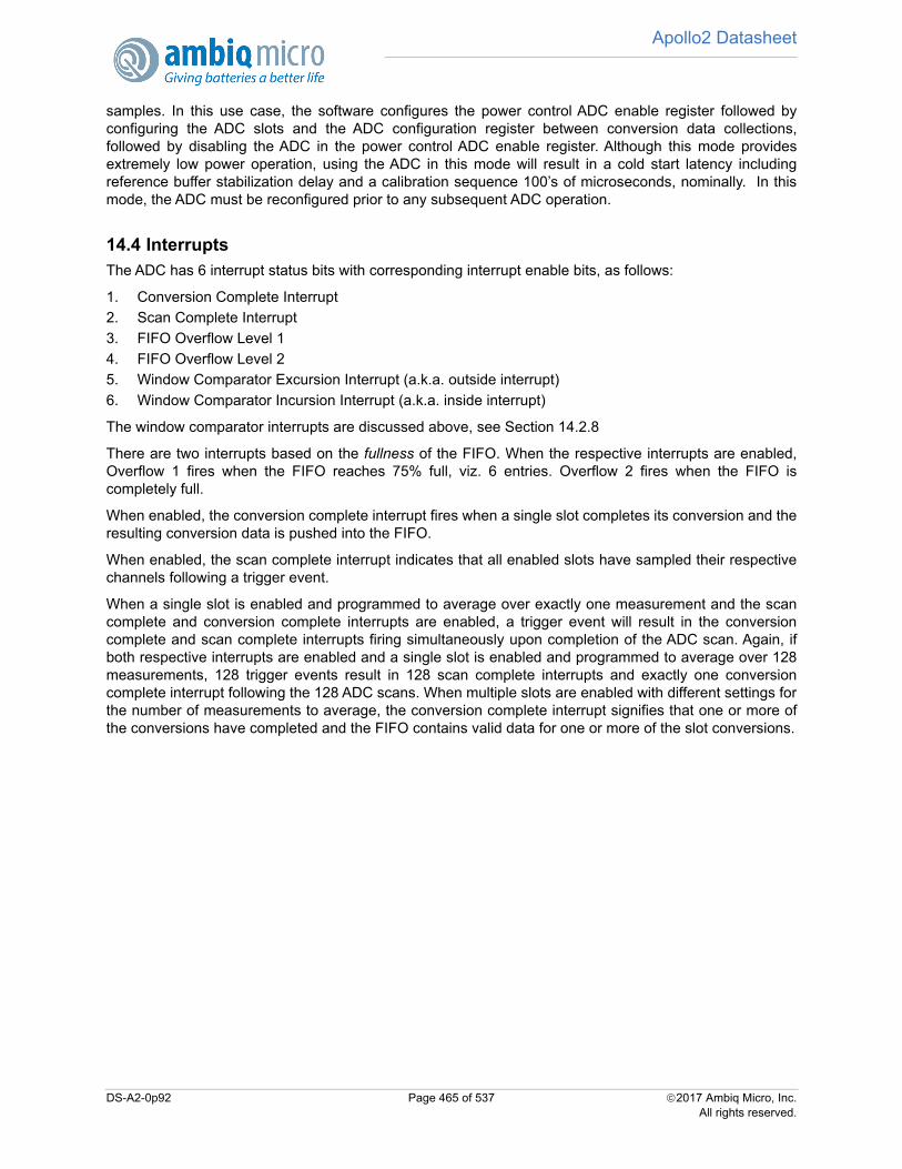
Apollo2 Datasheet
samples. In this use case, the software configures the power control ADC enable register followed byconfiguring the ADC slots and the ADC configuration register between conversion data collections,followed by disabling the ADC in the power control ADC enable register. Although this mode providesextremely low power operation, using the ADC in this mode will result in a cold start latency includingreference buffer stabilization delay and a calibration sequence 100’s of microseconds, nominally. In thismode, the ADC must be reconfigured prior to any subsequent ADC operation.
14.4 InterruptsThe ADC has 6 interrupt status bits with corresponding interrupt enable bits, as follows:
1. Conversion Complete Interrupt
2. Scan Complete Interrupt
3. FIFO Overflow Level 1
4. FIFO Overflow Level 2
5. Window Comparator Excursion Interrupt (a.k.a. outside interrupt)
6. Window Comparator Incursion Interrupt (a.k.a. inside interrupt)
The window comparator interrupts are discussed above, see Section 14.2.8
There are two interrupts based on the fullness of the FIFO. When the respective interrupts are enabled,Overflow 1 fires when the FIFO reaches 75% full, viz. 6 entries. Overflow 2 fires when the FIFO iscompletely full.
When enabled, the conversion complete interrupt fires when a single slot completes its conversion and theresulting conversion data is pushed into the FIFO.
When enabled, the scan complete interrupt indicates that all enabled slots have sampled their respectivechannels following a trigger event.
When a single slot is enabled and programmed to average over exactly one measurement and the scancomplete and conversion complete interrupts are enabled, a trigger event will result in the conversioncomplete and scan complete interrupts firing simultaneously upon completion of the ADC scan. Again, ifboth respective interrupts are enabled and a single slot is enabled and programmed to average over 128measurements, 128 trigger events result in 128 scan complete interrupts and exactly one conversioncomplete interrupt following the 128 ADC scans. When multiple slots are enabled with different settings forthe number of measurements to average, the conversion complete interrupt signifies that one or more ofthe conversions have completed and the FIFO contains valid data for one or more of the slot conversions.
DS-A2-0p92 Page 465 of 537 2017 Ambiq Micro, Inc.All rights reserved.
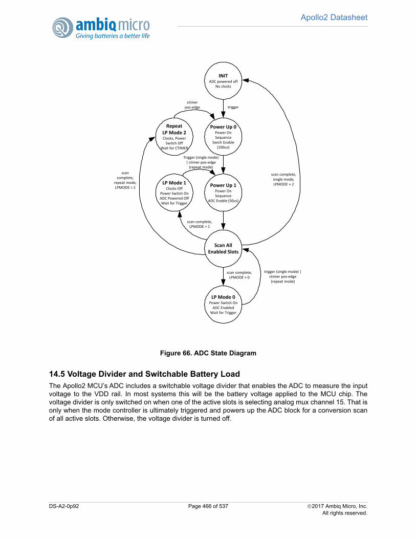
Apollo2 Datasheet
Figure 66. ADC State Diagram
14.5 Voltage Divider and Switchable Battery LoadThe Apollo2 MCU’s ADC includes a switchable voltage divider that enables the ADC to measure the inputvoltage to the VDD rail. In most systems this will be the battery voltage applied to the MCU chip. Thevoltage divider is only switched on when one of the active slots is selecting analog mux channel 15. That isonly when the mode controller is ultimately triggered and powers up the ADC block for a conversion scanof all active slots. Otherwise, the voltage divider is turned off.
INITADC powered off
No clocks
Power Up 0Power On Sequence
Swich Enable (100us)
Scan All Enabled Slots
LP Mode 1Clocks Off
Power Switch OnADC Powered OffWait for Trigger
Power Up 1Power On Sequence
ADC Enable (50us)
RepeatLP Mode 2Clocks, Power
Switch OffWait for CTIMER
LP Mode 0Power Switch On
ADC EnabledWait for Trigger
triggerctimer
pos‐edge
Trigger (single mode) | ctimer pos‐edge
(repeat mode)
scan complete, LPMODE = 0
scan complete, single mode, LPMODE = 2
scan complete, LPMODE = 1
scan complete,
repeat mode, LPMODE = 2
trigger (single mode) | ctimer pos‐edge (repeat mode)
DS-A2-0p92 Page 466 of 537 2017 Ambiq Micro, Inc.All rights reserved.
Apollo2 Datasheet
Figure 67. Switchable Battery Load
The switchable load resistor is enabled by the BATTLOAD bit as shown in Table 145, “ADCBATTLOADRegister,” on page 111.
This feature is used to help estimate the health of the battery chemistry by estimating the internalresistance of the battery.
14.6 ADC RegistersAnalog Digital Converter Control
INSTANCE 0 BASE ADDRESS:0x50010000
This is the detailed description of the Analog Digital Converter Register Block. The ADC Register Blockcontains the software control for enablement, slot configuration, clock configuration, trigger configuration,temperature sensor enablement, power modes, accumulate/divide, window comparison and interruptcontrol for the ADC functional unit.
ADC
ADC_I0 ...
ADC_I9
VDDVSS
...
Temp Sensor VIN
Select Ch 0xD
Input Voltage
BATTLOADRon≈ 500Ω
≈ 1/3
10K
Ω
5KΩ
ADC_DIFF0ADC_DIFF1
DS-A2-0p92 Page 467 of 537 2017 Ambiq Micro, Inc.All rights reserved.
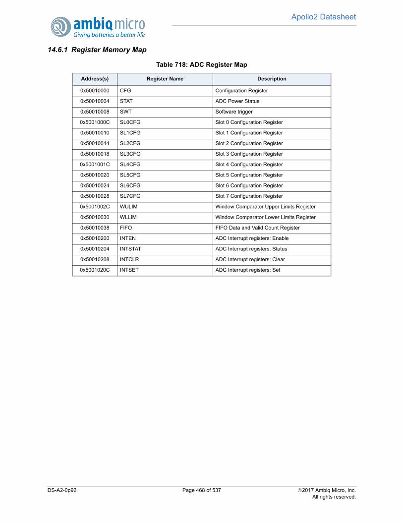
Apollo2 Datasheet
14.6.1 Register Memory Map
Table 718: ADC Register Map
Address(s) Register Name Description
0x50010000 CFG Configuration Register
0x50010004 STAT ADC Power Status
0x50010008 SWT Software trigger
0x5001000C SL0CFG Slot 0 Configuration Register
0x50010010 SL1CFG Slot 1 Configuration Register
0x50010014 SL2CFG Slot 2 Configuration Register
0x50010018 SL3CFG Slot 3 Configuration Register
0x5001001C SL4CFG Slot 4 Configuration Register
0x50010020 SL5CFG Slot 5 Configuration Register
0x50010024 SL6CFG Slot 6 Configuration Register
0x50010028 SL7CFG Slot 7 Configuration Register
0x5001002C WULIM Window Comparator Upper Limits Register
0x50010030 WLLIM Window Comparator Lower Limits Register
0x50010038 FIFO FIFO Data and Valid Count Register
0x50010200 INTEN ADC Interrupt registers: Enable
0x50010204 INTSTAT ADC Interrupt registers: Status
0x50010208 INTCLR ADC Interrupt registers: Clear
0x5001020C INTSET ADC Interrupt registers: Set
DS-A2-0p92 Page 468 of 537 2017 Ambiq Micro, Inc.All rights reserved.
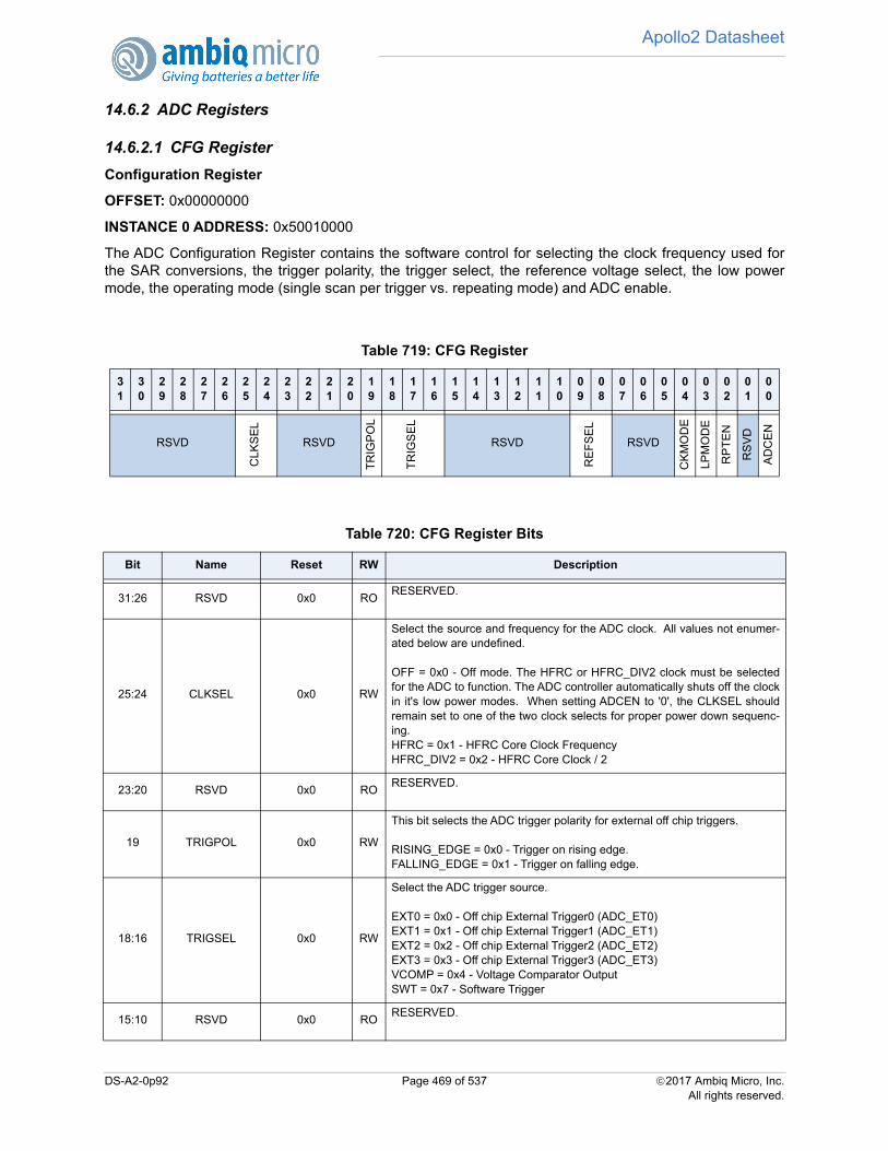
Apollo2 Datasheet
14.6.2 ADC Registers
14.6.2.1 CFG Register
Configuration Register
OFFSET: 0x00000000
INSTANCE 0 ADDRESS: 0x50010000
The ADC Configuration Register contains the software control for selecting the clock frequency used forthe SAR conversions, the trigger polarity, the trigger select, the reference voltage select, the low powermode, the operating mode (single scan per trigger vs. repeating mode) and ADC enable.
Table 719: CFG Register
31
30
29
28
27
26
25
24
23
22
21
20
19
18
17
16
15
14
13
12
11
10
09
08
07
06
05
04
03
02
01
00
RSVD
CLK
SE
L
RSVD
TR
IGP
OL
TR
IGS
EL
RSVD
RE
FS
EL
RSVD
CK
MO
DE
LPM
OD
E
RP
TE
N
RS
VD
AD
CE
N
Table 720: CFG Register Bits
Bit Name Reset RW Description
31:26 RSVD 0x0 RORESERVED.
25:24 CLKSEL 0x0 RW
Select the source and frequency for the ADC clock. All values not enumer-ated below are undefined.
OFF = 0x0 - Off mode. The HFRC or HFRC_DIV2 clock must be selectedfor the ADC to function. The ADC controller automatically shuts off the clockin it's low power modes. When setting ADCEN to '0', the CLKSEL shouldremain set to one of the two clock selects for proper power down sequenc-ing.HFRC = 0x1 - HFRC Core Clock FrequencyHFRC_DIV2 = 0x2 - HFRC Core Clock / 2
23:20 RSVD 0x0 RORESERVED.
19 TRIGPOL 0x0 RW
This bit selects the ADC trigger polarity for external off chip triggers.
RISING_EDGE = 0x0 - Trigger on rising edge.FALLING_EDGE = 0x1 - Trigger on falling edge.
18:16 TRIGSEL 0x0 RW
Select the ADC trigger source.
EXT0 = 0x0 - Off chip External Trigger0 (ADC_ET0)EXT1 = 0x1 - Off chip External Trigger1 (ADC_ET1)EXT2 = 0x2 - Off chip External Trigger2 (ADC_ET2)EXT3 = 0x3 - Off chip External Trigger3 (ADC_ET3)VCOMP = 0x4 - Voltage Comparator OutputSWT = 0x7 - Software Trigger
15:10 RSVD 0x0 RORESERVED.
DS-A2-0p92 Page 469 of 537 2017 Ambiq Micro, Inc.All rights reserved.
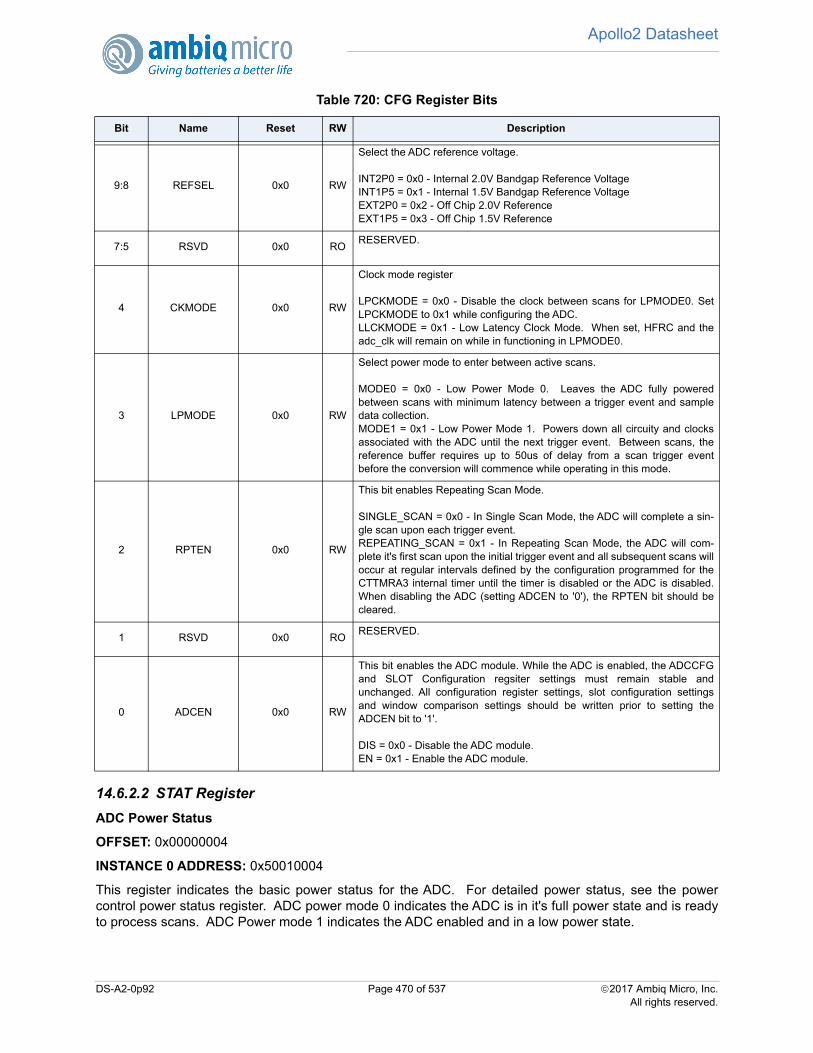
Apollo2 Datasheet
14.6.2.2 STAT Register
ADC Power Status
OFFSET: 0x00000004
INSTANCE 0 ADDRESS: 0x50010004
This register indicates the basic power status for the ADC. For detailed power status, see the powercontrol power status register. ADC power mode 0 indicates the ADC is in it's full power state and is readyto process scans. ADC Power mode 1 indicates the ADC enabled and in a low power state.
9:8 REFSEL 0x0 RW
Select the ADC reference voltage.
INT2P0 = 0x0 - Internal 2.0V Bandgap Reference VoltageINT1P5 = 0x1 - Internal 1.5V Bandgap Reference VoltageEXT2P0 = 0x2 - Off Chip 2.0V ReferenceEXT1P5 = 0x3 - Off Chip 1.5V Reference
7:5 RSVD 0x0 RORESERVED.
4 CKMODE 0x0 RW
Clock mode register
LPCKMODE = 0x0 - Disable the clock between scans for LPMODE0. SetLPCKMODE to 0x1 while configuring the ADC.LLCKMODE = 0x1 - Low Latency Clock Mode. When set, HFRC and theadc_clk will remain on while in functioning in LPMODE0.
3 LPMODE 0x0 RW
Select power mode to enter between active scans.
MODE0 = 0x0 - Low Power Mode 0. Leaves the ADC fully poweredbetween scans with minimum latency between a trigger event and sampledata collection.MODE1 = 0x1 - Low Power Mode 1. Powers down all circuity and clocksassociated with the ADC until the next trigger event. Between scans, thereference buffer requires up to 50us of delay from a scan trigger eventbefore the conversion will commence while operating in this mode.
2 RPTEN 0x0 RW
This bit enables Repeating Scan Mode.
SINGLE_SCAN = 0x0 - In Single Scan Mode, the ADC will complete a sin-gle scan upon each trigger event.REPEATING_SCAN = 0x1 - In Repeating Scan Mode, the ADC will com-plete it's first scan upon the initial trigger event and all subsequent scans willoccur at regular intervals defined by the configuration programmed for theCTTMRA3 internal timer until the timer is disabled or the ADC is disabled.When disabling the ADC (setting ADCEN to '0'), the RPTEN bit should becleared.
1 RSVD 0x0 RORESERVED.
0 ADCEN 0x0 RW
This bit enables the ADC module. While the ADC is enabled, the ADCCFGand SLOT Configuration regsiter settings must remain stable andunchanged. All configuration register settings, slot configuration settingsand window comparison settings should be written prior to setting theADCEN bit to '1'.
DIS = 0x0 - Disable the ADC module.EN = 0x1 - Enable the ADC module.
Table 720: CFG Register Bits
Bit Name Reset RW Description
DS-A2-0p92 Page 470 of 537 2017 Ambiq Micro, Inc.All rights reserved.
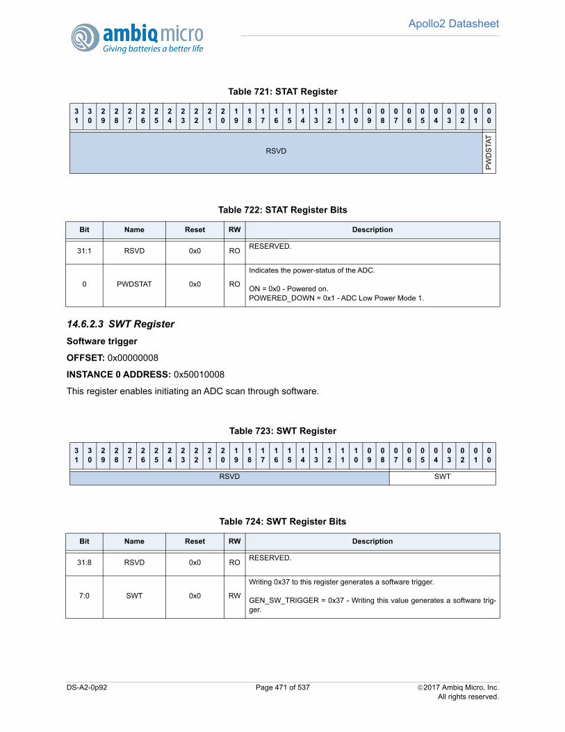
Apollo2 Datasheet
14.6.2.3 SWT Register
Software trigger
OFFSET: 0x00000008
INSTANCE 0 ADDRESS: 0x50010008
This register enables initiating an ADC scan through software.
Table 721: STAT Register
31
30
29
28
27
26
25
24
23
22
21
20
19
18
17
16
15
14
13
12
11
10
09
08
07
06
05
04
03
02
01
00
RSVD
PW
DS
TAT
Table 722: STAT Register Bits
Bit Name Reset RW Description
31:1 RSVD 0x0 RORESERVED.
0 PWDSTAT 0x0 RO
Indicates the power-status of the ADC.
ON = 0x0 - Powered on.POWERED_DOWN = 0x1 - ADC Low Power Mode 1.
Table 723: SWT Register
31
30
29
28
27
26
25
24
23
22
21
20
19
18
17
16
15
14
13
12
11
10
09
08
07
06
05
04
03
02
01
00
RSVD SWT
Table 724: SWT Register Bits
Bit Name Reset RW Description
31:8 RSVD 0x0 RORESERVED.
7:0 SWT 0x0 RW
Writing 0x37 to this register generates a software trigger.
GEN_SW_TRIGGER = 0x37 - Writing this value generates a software trig-ger.
DS-A2-0p92 Page 471 of 537 2017 Ambiq Micro, Inc.All rights reserved.

Apollo2 Datasheet
14.6.2.4 SL0CFG Register
Slot 0 Configuration Register
OFFSET: 0x0000000C
INSTANCE 0 ADDRESS: 0x5001000C
Slot 0 Configuration Register
Table 725: SL0CFG Register
31
30
29
28
27
26
25
24
23
22
21
20
19
18
17
16
15
14
13
12
11
10
09
08
07
06
05
04
03
02
01
00
RSVD
AD
SE
L0
RSVD
PR
MO
DE
0
RSVD CHSEL0 RSVD
WC
EN
0
SLE
N0
Table 726: SL0CFG Register Bits
Bit Name Reset RW Description
31:27 RSVD 0x0 RORESERVED.
26:24 ADSEL0 0x0 RW
Select the number of measurements to average in the accumulate dividemodule for this slot.
AVG_1_MSRMT = 0x0 - Average in 1 measurement in the accumulatedivide module for this slot.AVG_2_MSRMTS = 0x1 - Average in 2 measurements in the accumulatedivide module for this slot.AVG_4_MSRMTS = 0x2 - Average in 4 measurements in the accumulatedivide module for this slot.AVG_8_MSRMT = 0x3 - Average in 8 measurements in the accumulatedivide module for this slot.AVG_16_MSRMTS = 0x4 - Average in 16 measurements in the accumulatedivide module for this slot.AVG_32_MSRMTS = 0x5 - Average in 32 measurements in the accumulatedivide module for this slot.AVG_64_MSRMTS = 0x6 - Average in 64 measurements in the accumulatedivide module for this slot.AVG_128_MSRMTS = 0x7 - Average in 128 measurements in the accumu-late divide module for this slot.
23:18 RSVD 0x0 RORESERVED.
17:16 PRMODE0 0x0 RW
Set the Precision Mode For Slot.
P14B = 0x0 - 14-bit precision modeP12B = 0x1 - 12-bit precision modeP10B = 0x2 - 10-bit precision modeP8B = 0x3 - 8-bit precision mode
15:12 RSVD 0x0 RORESERVED.
DS-A2-0p92 Page 472 of 537 2017 Ambiq Micro, Inc.All rights reserved.

Apollo2 Datasheet
14.6.2.5 SL1CFG Register
Slot 1 Configuration Register
OFFSET: 0x00000010
INSTANCE 0 ADDRESS: 0x50010010
Slot 1 Configuration Register
11:8 CHSEL0 0x0 RW
Select one of the 14 channel inputs for this slot.
SE0 = 0x0 - single ended external GPIO connection to pad16.SE1 = 0x1 - single ended external GPIO connection to pad29.SE2 = 0x2 - single ended external GPIO connection to pad11.SE3 = 0x3 - single ended external GPIO connection to pad31.SE4 = 0x4 - single ended external GPIO connection to pad32.SE5 = 0x5 - single ended external GPIO connection to pad33.SE6 = 0x6 - single ended external GPIO connection to pad34.SE7 = 0x7 - single ended external GPIO connection to pad35.SE8 = 0x8 - single ended external GPIO connection to pad13.SE9 = 0x9 - single ended external GPIO connection to pad12.DF0 = 0xA - differential external GPIO connections to pad12(N) andpad13(P).DF1 = 0xB - differential external GPIO connections to pad15(N) andpad14(P).TEMP = 0xC - internal temperature sensor.BATT = 0xD - internal voltage divide-by-3 connection.VSS = 0xE - VSS
7:2 RSVD 0x0 RORESERVED.
1 WCEN0 0x0 RWThis bit enables the window compare function for slot 0.
WCEN = 0x1 - Enable the window compare for slot 0.
0 SLEN0 0x0 RWThis bit enables slot 0 for ADC conversions.
SLEN = 0x1 - Enable slot 0 for ADC conversions.
Table 727: SL1CFG Register
31
30
29
28
27
26
25
24
23
22
21
20
19
18
17
16
15
14
13
12
11
10
09
08
07
06
05
04
03
02
01
00
RSVD
AD
SE
L1
RSVD
PR
MO
DE
1
RSVD CHSEL1 RSVD
WC
EN
1
SLE
N1
Table 726: SL0CFG Register Bits
Bit Name Reset RW Description
DS-A2-0p92 Page 473 of 537 2017 Ambiq Micro, Inc.All rights reserved.
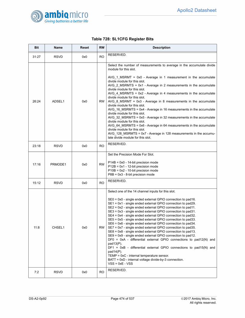
Apollo2 Datasheet
Table 728: SL1CFG Register Bits
Bit Name Reset RW Description
31:27 RSVD 0x0 RORESERVED.
26:24 ADSEL1 0x0 RW
Select the number of measurements to average in the accumulate dividemodule for this slot.
AVG_1_MSRMT = 0x0 - Average in 1 measurement in the accumulatedivide module for this slot.AVG_2_MSRMTS = 0x1 - Average in 2 measurements in the accumulatedivide module for this slot.AVG_4_MSRMTS = 0x2 - Average in 4 measurements in the accumulatedivide module for this slot.AVG_8_MSRMT = 0x3 - Average in 8 measurements in the accumulatedivide module for this slot.AVG_16_MSRMTS = 0x4 - Average in 16 measurements in the accumulatedivide module for this slot.AVG_32_MSRMTS = 0x5 - Average in 32 measurements in the accumulatedivide module for this slot.AVG_64_MSRMTS = 0x6 - Average in 64 measurements in the accumulatedivide module for this slot.AVG_128_MSRMTS = 0x7 - Average in 128 measurements in the accumu-late divide module for this slot.
23:18 RSVD 0x0 RORESERVED.
17:16 PRMODE1 0x0 RW
Set the Precision Mode For Slot.
P14B = 0x0 - 14-bit precision modeP12B = 0x1 - 12-bit precision modeP10B = 0x2 - 10-bit precision modeP8B = 0x3 - 8-bit precision mode
15:12 RSVD 0x0 RORESERVED.
11:8 CHSEL1 0x0 RW
Select one of the 14 channel inputs for this slot.
SE0 = 0x0 - single ended external GPIO connection to pad16.SE1 = 0x1 - single ended external GPIO connection to pad29.SE2 = 0x2 - single ended external GPIO connection to pad11.SE3 = 0x3 - single ended external GPIO connection to pad31.SE4 = 0x4 - single ended external GPIO connection to pad32.SE5 = 0x5 - single ended external GPIO connection to pad33.SE6 = 0x6 - single ended external GPIO connection to pad34.SE7 = 0x7 - single ended external GPIO connection to pad35.SE8 = 0x8 - single ended external GPIO connection to pad13.SE9 = 0x9 - single ended external GPIO connection to pad12.DF0 = 0xA - differential external GPIO connections to pad12(N) andpad13(P).DF1 = 0xB - differential external GPIO connections to pad15(N) andpad14(P).TEMP = 0xC - internal temperature sensor.BATT = 0xD - internal voltage divide-by-3 connection.VSS = 0xE - VSS
7:2 RSVD 0x0 RORESERVED.
DS-A2-0p92 Page 474 of 537 2017 Ambiq Micro, Inc.All rights reserved.
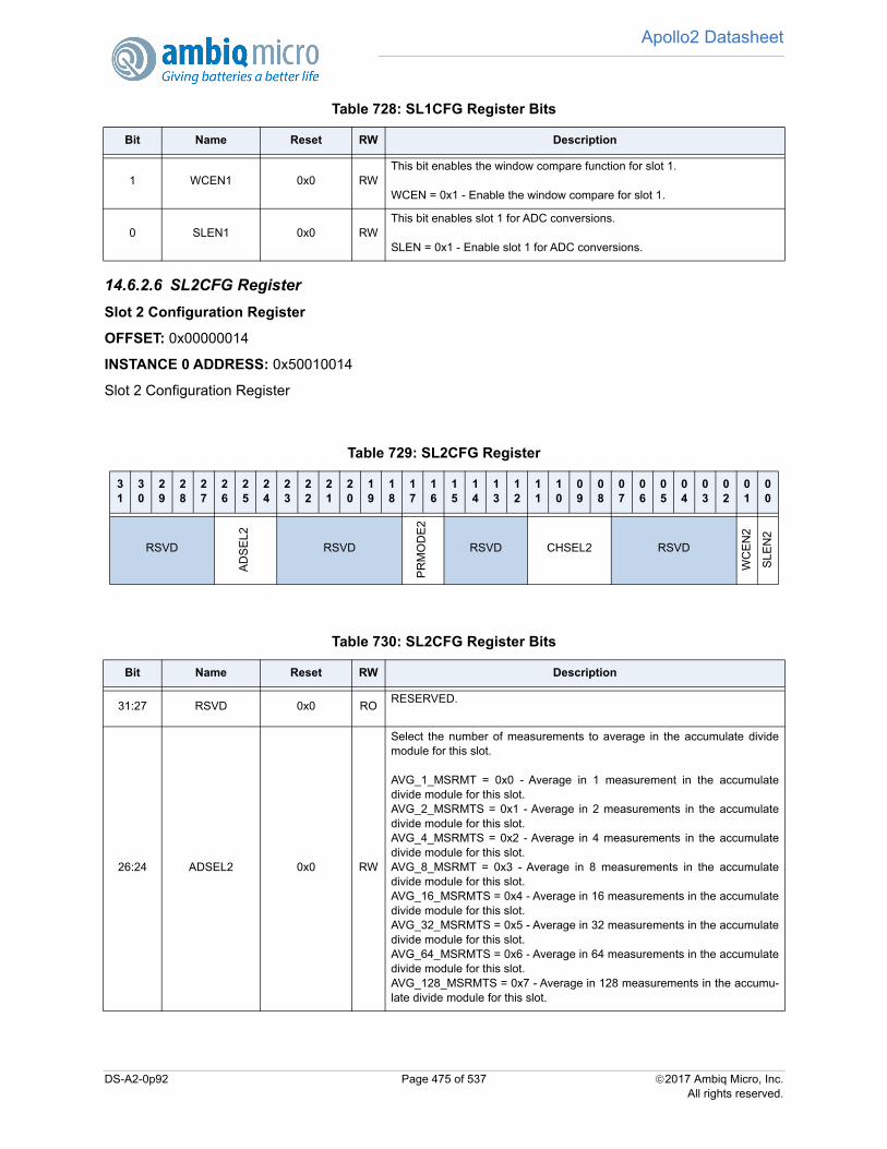
Apollo2 Datasheet
14.6.2.6 SL2CFG Register
Slot 2 Configuration Register
OFFSET: 0x00000014
INSTANCE 0 ADDRESS: 0x50010014
Slot 2 Configuration Register
1 WCEN1 0x0 RWThis bit enables the window compare function for slot 1.
WCEN = 0x1 - Enable the window compare for slot 1.
0 SLEN1 0x0 RWThis bit enables slot 1 for ADC conversions.
SLEN = 0x1 - Enable slot 1 for ADC conversions.
Table 729: SL2CFG Register
31
30
29
28
27
26
25
24
23
22
21
20
19
18
17
16
15
14
13
12
11
10
09
08
07
06
05
04
03
02
01
00
RSVD
AD
SE
L2
RSVD
PR
MO
DE
2
RSVD CHSEL2 RSVD
WC
EN
2
SLE
N2
Table 730: SL2CFG Register Bits
Bit Name Reset RW Description
31:27 RSVD 0x0 RORESERVED.
26:24 ADSEL2 0x0 RW
Select the number of measurements to average in the accumulate dividemodule for this slot.
AVG_1_MSRMT = 0x0 - Average in 1 measurement in the accumulatedivide module for this slot.AVG_2_MSRMTS = 0x1 - Average in 2 measurements in the accumulatedivide module for this slot.AVG_4_MSRMTS = 0x2 - Average in 4 measurements in the accumulatedivide module for this slot.AVG_8_MSRMT = 0x3 - Average in 8 measurements in the accumulatedivide module for this slot.AVG_16_MSRMTS = 0x4 - Average in 16 measurements in the accumulatedivide module for this slot.AVG_32_MSRMTS = 0x5 - Average in 32 measurements in the accumulatedivide module for this slot.AVG_64_MSRMTS = 0x6 - Average in 64 measurements in the accumulatedivide module for this slot.AVG_128_MSRMTS = 0x7 - Average in 128 measurements in the accumu-late divide module for this slot.
Table 728: SL1CFG Register Bits
Bit Name Reset RW Description
DS-A2-0p92 Page 475 of 537 2017 Ambiq Micro, Inc.All rights reserved.
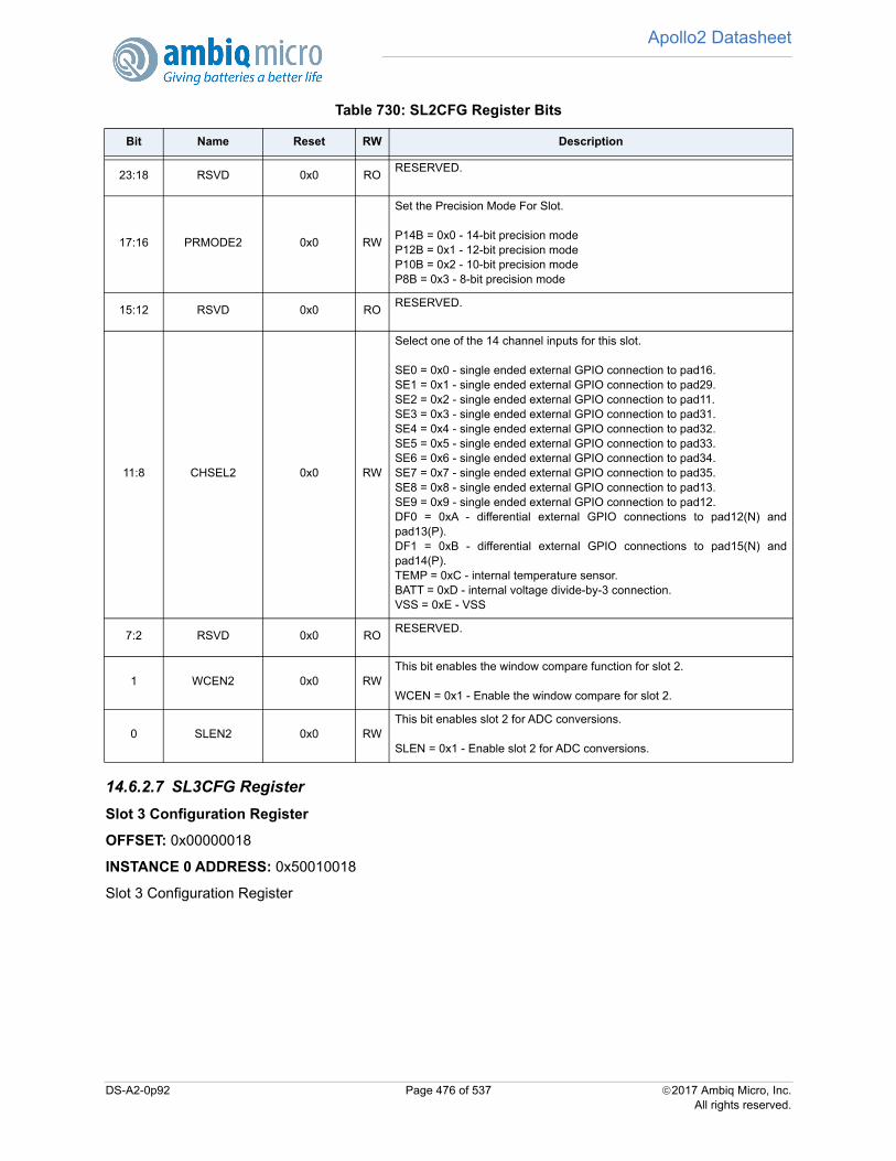
Apollo2 Datasheet
14.6.2.7 SL3CFG Register
Slot 3 Configuration Register
OFFSET: 0x00000018
INSTANCE 0 ADDRESS: 0x50010018
Slot 3 Configuration Register
23:18 RSVD 0x0 RORESERVED.
17:16 PRMODE2 0x0 RW
Set the Precision Mode For Slot.
P14B = 0x0 - 14-bit precision modeP12B = 0x1 - 12-bit precision modeP10B = 0x2 - 10-bit precision modeP8B = 0x3 - 8-bit precision mode
15:12 RSVD 0x0 RORESERVED.
11:8 CHSEL2 0x0 RW
Select one of the 14 channel inputs for this slot.
SE0 = 0x0 - single ended external GPIO connection to pad16.SE1 = 0x1 - single ended external GPIO connection to pad29.SE2 = 0x2 - single ended external GPIO connection to pad11.SE3 = 0x3 - single ended external GPIO connection to pad31.SE4 = 0x4 - single ended external GPIO connection to pad32.SE5 = 0x5 - single ended external GPIO connection to pad33.SE6 = 0x6 - single ended external GPIO connection to pad34.SE7 = 0x7 - single ended external GPIO connection to pad35.SE8 = 0x8 - single ended external GPIO connection to pad13.SE9 = 0x9 - single ended external GPIO connection to pad12.DF0 = 0xA - differential external GPIO connections to pad12(N) andpad13(P).DF1 = 0xB - differential external GPIO connections to pad15(N) andpad14(P).TEMP = 0xC - internal temperature sensor.BATT = 0xD - internal voltage divide-by-3 connection.VSS = 0xE - VSS
7:2 RSVD 0x0 RORESERVED.
1 WCEN2 0x0 RWThis bit enables the window compare function for slot 2.
WCEN = 0x1 - Enable the window compare for slot 2.
0 SLEN2 0x0 RWThis bit enables slot 2 for ADC conversions.
SLEN = 0x1 - Enable slot 2 for ADC conversions.
Table 730: SL2CFG Register Bits
Bit Name Reset RW Description
DS-A2-0p92 Page 476 of 537 2017 Ambiq Micro, Inc.All rights reserved.
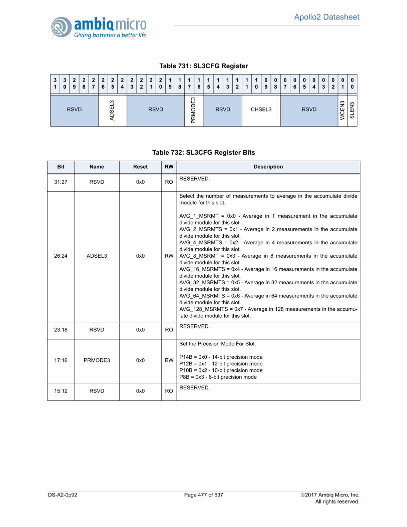
Apollo2 Datasheet
Table 731: SL3CFG Register
31
30
29
28
27
26
25
24
23
22
21
20
19
18
17
16
15
14
13
12
11
10
09
08
07
06
05
04
03
02
01
00
RSVDA
DS
EL3
RSVD
PR
MO
DE
3
RSVD CHSEL3 RSVD
WC
EN
3
SLE
N3
Table 732: SL3CFG Register Bits
Bit Name Reset RW Description
31:27 RSVD 0x0 RORESERVED.
26:24 ADSEL3 0x0 RW
Select the number of measurements to average in the accumulate dividemodule for this slot.
AVG_1_MSRMT = 0x0 - Average in 1 measurement in the accumulatedivide module for this slot.AVG_2_MSRMTS = 0x1 - Average in 2 measurements in the accumulatedivide module for this slot.AVG_4_MSRMTS = 0x2 - Average in 4 measurements in the accumulatedivide module for this slot.AVG_8_MSRMT = 0x3 - Average in 8 measurements in the accumulatedivide module for this slot.AVG_16_MSRMTS = 0x4 - Average in 16 measurements in the accumulatedivide module for this slot.AVG_32_MSRMTS = 0x5 - Average in 32 measurements in the accumulatedivide module for this slot.AVG_64_MSRMTS = 0x6 - Average in 64 measurements in the accumulatedivide module for this slot.AVG_128_MSRMTS = 0x7 - Average in 128 measurements in the accumu-late divide module for this slot.
23:18 RSVD 0x0 RORESERVED.
17:16 PRMODE3 0x0 RW
Set the Precision Mode For Slot.
P14B = 0x0 - 14-bit precision modeP12B = 0x1 - 12-bit precision modeP10B = 0x2 - 10-bit precision modeP8B = 0x3 - 8-bit precision mode
15:12 RSVD 0x0 RORESERVED.
DS-A2-0p92 Page 477 of 537 2017 Ambiq Micro, Inc.All rights reserved.
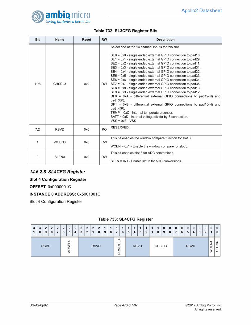
Apollo2 Datasheet
14.6.2.8 SL4CFG Register
Slot 4 Configuration Register
OFFSET: 0x0000001C
INSTANCE 0 ADDRESS: 0x5001001C
Slot 4 Configuration Register
11:8 CHSEL3 0x0 RW
Select one of the 14 channel inputs for this slot.
SE0 = 0x0 - single ended external GPIO connection to pad16.SE1 = 0x1 - single ended external GPIO connection to pad29.SE2 = 0x2 - single ended external GPIO connection to pad11.SE3 = 0x3 - single ended external GPIO connection to pad31.SE4 = 0x4 - single ended external GPIO connection to pad32.SE5 = 0x5 - single ended external GPIO connection to pad33.SE6 = 0x6 - single ended external GPIO connection to pad34.SE7 = 0x7 - single ended external GPIO connection to pad35.SE8 = 0x8 - single ended external GPIO connection to pad13.SE9 = 0x9 - single ended external GPIO connection to pad12.DF0 = 0xA - differential external GPIO connections to pad12(N) andpad13(P).DF1 = 0xB - differential external GPIO connections to pad15(N) andpad14(P).TEMP = 0xC - internal temperature sensor.BATT = 0xD - internal voltage divide-by-3 connection.VSS = 0xE - VSS
7:2 RSVD 0x0 RORESERVED.
1 WCEN3 0x0 RWThis bit enables the window compare function for slot 3.
WCEN = 0x1 - Enable the window compare for slot 3.
0 SLEN3 0x0 RWThis bit enables slot 3 for ADC conversions.
SLEN = 0x1 - Enable slot 3 for ADC conversions.
Table 733: SL4CFG Register
31
30
29
28
27
26
25
24
23
22
21
20
19
18
17
16
15
14
13
12
11
10
09
08
07
06
05
04
03
02
01
00
RSVD
AD
SE
L4
RSVD
PR
MO
DE
4
RSVD CHSEL4 RSVD
WC
EN
4
SLE
N4
Table 732: SL3CFG Register Bits
Bit Name Reset RW Description
DS-A2-0p92 Page 478 of 537 2017 Ambiq Micro, Inc.All rights reserved.

Apollo2 Datasheet
Table 734: SL4CFG Register Bits
Bit Name Reset RW Description
31:27 RSVD 0x0 RORESERVED.
26:24 ADSEL4 0x0 RW
Select the number of measurements to average in the accumulate dividemodule for this slot.
AVG_1_MSRMT = 0x0 - Average in 1 measurement in the accumulatedivide module for this slot.AVG_2_MSRMTS = 0x1 - Average in 2 measurements in the accumulatedivide module for this slot.AVG_4_MSRMTS = 0x2 - Average in 4 measurements in the accumulatedivide module for this slot.AVG_8_MSRMT = 0x3 - Average in 8 measurements in the accumulatedivide module for this slot.AVG_16_MSRMTS = 0x4 - Average in 16 measurements in the accumulatedivide module for this slot.AVG_32_MSRMTS = 0x5 - Average in 32 measurements in the accumulatedivide module for this slot.AVG_64_MSRMTS = 0x6 - Average in 64 measurements in the accumulatedivide module for this slot.AVG_128_MSRMTS = 0x7 - Average in 128 measurements in the accumu-late divide module for this slot.
23:18 RSVD 0x0 RORESERVED.
17:16 PRMODE4 0x0 RW
Set the Precision Mode For Slot.
P14B = 0x0 - 14-bit precision modeP12B = 0x1 - 12-bit precision modeP10B = 0x2 - 10-bit precision modeP8B = 0x3 - 8-bit precision mode
15:12 RSVD 0x0 RORESERVED.
11:8 CHSEL4 0x0 RW
Select one of the 14 channel inputs for this slot.
SE0 = 0x0 - single ended external GPIO connection to pad16.SE1 = 0x1 - single ended external GPIO connection to pad29.SE2 = 0x2 - single ended external GPIO connection to pad11.SE3 = 0x3 - single ended external GPIO connection to pad31.SE4 = 0x4 - single ended external GPIO connection to pad32.SE5 = 0x5 - single ended external GPIO connection to pad33.SE6 = 0x6 - single ended external GPIO connection to pad34.SE7 = 0x7 - single ended external GPIO connection to pad35.SE8 = 0x8 - single ended external GPIO connection to pad13.SE9 = 0x9 - single ended external GPIO connection to pad12.DF0 = 0xA - differential external GPIO connections to pad12(N) andpad13(P).DF1 = 0xB - differential external GPIO connections to pad15(N) andpad14(P).TEMP = 0xC - internal temperature sensor.BATT = 0xD - internal voltage divide-by-3 connection.VSS = 0xE - VSS
7:2 RSVD 0x0 RORESERVED.
DS-A2-0p92 Page 479 of 537 2017 Ambiq Micro, Inc.All rights reserved.

Apollo2 Datasheet
14.6.2.9 SL5CFG Register
Slot 5 Configuration Register
OFFSET: 0x00000020
INSTANCE 0 ADDRESS: 0x50010020
Slot 5 Configuration Register
1 WCEN4 0x0 RWThis bit enables the window compare function for slot 4.
WCEN = 0x1 - Enable the window compare for slot 4.
0 SLEN4 0x0 RWThis bit enables slot 4 for ADC conversions.
SLEN = 0x1 - Enable slot 4 for ADC conversions.
Table 735: SL5CFG Register
31
30
29
28
27
26
25
24
23
22
21
20
19
18
17
16
15
14
13
12
11
10
09
08
07
06
05
04
03
02
01
00
RSVD
AD
SE
L5
RSVD
PR
MO
DE
5
RSVD CHSEL5 RSVD
WC
EN
5
SLE
N5
Table 736: SL5CFG Register Bits
Bit Name Reset RW Description
31:27 RSVD 0x0 RORESERVED.
26:24 ADSEL5 0x0 RW
Select number of measurements to average in the accumulate divide mod-ule for this slot.
AVG_1_MSRMT = 0x0 - Average in 1 measurement in the accumulatedivide module for this slot.AVG_2_MSRMTS = 0x1 - Average in 2 measurements in the accumulatedivide module for this slot.AVG_4_MSRMTS = 0x2 - Average in 4 measurements in the accumulatedivide module for this slot.AVG_8_MSRMT = 0x3 - Average in 8 measurements in the accumulatedivide module for this slot.AVG_16_MSRMTS = 0x4 - Average in 16 measurements in the accumulatedivide module for this slot.AVG_32_MSRMTS = 0x5 - Average in 32 measurements in the accumulatedivide module for this slot.AVG_64_MSRMTS = 0x6 - Average in 64 measurements in the accumulatedivide module for this slot.AVG_128_MSRMTS = 0x7 - Average in 128 measurements in the accumu-late divide module for this slot.
Table 734: SL4CFG Register Bits
Bit Name Reset RW Description
DS-A2-0p92 Page 480 of 537 2017 Ambiq Micro, Inc.All rights reserved.

Apollo2 Datasheet
14.6.2.10SL6CFG Register
Slot 6 Configuration Register
OFFSET: 0x00000024
INSTANCE 0 ADDRESS: 0x50010024
Slot 6 Configuration Register
23:18 RSVD 0x0 RORESERVED.
17:16 PRMODE5 0x0 RW
Set the Precision Mode For Slot.
P14B = 0x0 - 14-bit precision modeP12B = 0x1 - 12-bit precision modeP10B = 0x2 - 10-bit precision modeP8B = 0x3 - 8-bit precision mode
15:12 RSVD 0x0 RORESERVED.
11:8 CHSEL5 0x0 RW
Select one of the 14 channel inputs for this slot.
SE0 = 0x0 - single ended external GPIO connection to pad16.SE1 = 0x1 - single ended external GPIO connection to pad29.SE2 = 0x2 - single ended external GPIO connection to pad11.SE3 = 0x3 - single ended external GPIO connection to pad31.SE4 = 0x4 - single ended external GPIO connection to pad32.SE5 = 0x5 - single ended external GPIO connection to pad33.SE6 = 0x6 - single ended external GPIO connection to pad34.SE7 = 0x7 - single ended external GPIO connection to pad35.SE8 = 0x8 - single ended external GPIO connection to pad13.SE9 = 0x9 - single ended external GPIO connection to pad12.DF0 = 0xA - differential external GPIO connections to pad12(N) andpad13(P).DF1 = 0xB - differential external GPIO connections to pad15(N) andpad14(P).TEMP = 0xC - internal temperature sensor.BATT = 0xD - internal voltage divide-by-3 connection.VSS = 0xE - VSS
7:2 RSVD 0x0 RORESERVED.
1 WCEN5 0x0 RWThis bit enables the window compare function for slot 5.
WCEN = 0x1 - Enable the window compare for slot 5.
0 SLEN5 0x0 RWThis bit enables slot 5 for ADC conversions.
SLEN = 0x1 - Enable slot 5 for ADC conversions.
Table 736: SL5CFG Register Bits
Bit Name Reset RW Description
DS-A2-0p92 Page 481 of 537 2017 Ambiq Micro, Inc.All rights reserved.

Apollo2 Datasheet
Table 737: SL6CFG Register
31
30
29
28
27
26
25
24
23
22
21
20
19
18
17
16
15
14
13
12
11
10
09
08
07
06
05
04
03
02
01
00
RSVDA
DS
EL6
RSVD
PR
MO
DE
6
RSVD CHSEL6 RSVD
WC
EN
6
SLE
N6
Table 738: SL6CFG Register Bits
Bit Name Reset RW Description
31:27 RSVD 0x0 RORESERVED.
26:24 ADSEL6 0x0 RW
Select the number of measurements to average in the accumulate dividemodule for this slot.
AVG_1_MSRMT = 0x0 - Average in 1 measurement in the accumulatedivide module for this slot.AVG_2_MSRMTS = 0x1 - Average in 2 measurements in the accumulatedivide module for this slot.AVG_4_MSRMTS = 0x2 - Average in 4 measurements in the accumulatedivide module for this slot.AVG_8_MSRMT = 0x3 - Average in 8 measurements in the accumulatedivide module for this slot.AVG_16_MSRMTS = 0x4 - Average in 16 measurements in the accumulatedivide module for this slot.AVG_32_MSRMTS = 0x5 - Average in 32 measurements in the accumulatedivide module for this slot.AVG_64_MSRMTS = 0x6 - Average in 64 measurements in the accumulatedivide module for this slot.AVG_128_MSRMTS = 0x7 - Average in 128 measurements in the accumu-late divide module for this slot.
23:18 RSVD 0x0 RORESERVED.
17:16 PRMODE6 0x0 RW
Set the Precision Mode For Slot.
P14B = 0x0 - 14-bit precision modeP12B = 0x1 - 12-bit precision modeP10B = 0x2 - 10-bit precision modeP8B = 0x3 - 8-bit precision mode
15:12 RSVD 0x0 RORESERVED.
DS-A2-0p92 Page 482 of 537 2017 Ambiq Micro, Inc.All rights reserved.

Apollo2 Datasheet
14.6.2.11SL7CFG Register
Slot 7 Configuration Register
OFFSET: 0x00000028
INSTANCE 0 ADDRESS: 0x50010028
Slot 7 Configuration Register
11:8 CHSEL6 0x0 RW
Select one of the 14 channel inputs for this slot.
SE0 = 0x0 - single ended external GPIO connection to pad16.SE1 = 0x1 - single ended external GPIO connection to pad29.SE2 = 0x2 - single ended external GPIO connection to pad11.SE3 = 0x3 - single ended external GPIO connection to pad31.SE4 = 0x4 - single ended external GPIO connection to pad32.SE5 = 0x5 - single ended external GPIO connection to pad33.SE6 = 0x6 - single ended external GPIO connection to pad34.SE7 = 0x7 - single ended external GPIO connection to pad35.SE8 = 0x8 - single ended external GPIO connection to pad13.SE9 = 0x9 - single ended external GPIO connection to pad12.DF0 = 0xA - differential external GPIO connections to pad12(N) andpad13(P).DF1 = 0xB - differential external GPIO connections to pad15(N) andpad14(P).TEMP = 0xC - internal temperature sensor.BATT = 0xD - internal voltage divide-by-3 connection.VSS = 0xE - VSS
7:2 RSVD 0x0 RORESERVED.
1 WCEN6 0x0 RWThis bit enables the window compare function for slot 6.
WCEN = 0x1 - Enable the window compare for slot 6.
0 SLEN6 0x0 RWThis bit enables slot 6 for ADC conversions.
SLEN = 0x1 - Enable slot 6 for ADC conversions.
Table 739: SL7CFG Register
31
30
29
28
27
26
25
24
23
22
21
20
19
18
17
16
15
14
13
12
11
10
09
08
07
06
05
04
03
02
01
00
RSVD
AD
SE
L7
RSVD
PR
MO
DE
7
RSVD CHSEL7 RSVD
WC
EN
7
SLE
N7
Table 738: SL6CFG Register Bits
Bit Name Reset RW Description
DS-A2-0p92 Page 483 of 537 2017 Ambiq Micro, Inc.All rights reserved.

Apollo2 Datasheet
Table 740: SL7CFG Register Bits
Bit Name Reset RW Description
31:27 RSVD 0x0 RORESERVED.
26:24 ADSEL7 0x0 RW
Select the number of measurements to average in the accumulate dividemodule for this slot.
AVG_1_MSRMT = 0x0 - Average in 1 measurement in the accumulatedivide module for this slot.AVG_2_MSRMTS = 0x1 - Average in 2 measurements in the accumulatedivide module for this slot.AVG_4_MSRMTS = 0x2 - Average in 4 measurements in the accumulatedivide module for this slot.AVG_8_MSRMT = 0x3 - Average in 8 measurements in the accumulatedivide module for this slot.AVG_16_MSRMTS = 0x4 - Average in 16 measurements in the accumulatedivide module for this slot.AVG_32_MSRMTS = 0x5 - Average in 32 measurements in the accumulatedivide module for this slot.AVG_64_MSRMTS = 0x6 - Average in 64 measurements in the accumulatedivide module for this slot.AVG_128_MSRMTS = 0x7 - Average in 128 measurements in the accumu-late divide module for this slot.
23:18 RSVD 0x0 RORESERVED.
17:16 PRMODE7 0x0 RW
Set the Precision Mode For Slot.
P14B = 0x0 - 14-bit precision modeP12B = 0x1 - 12-bit precision modeP10B = 0x2 - 10-bit precision modeP8B = 0x3 - 8-bit precision mode
15:12 RSVD 0x0 RORESERVED.
11:8 CHSEL7 0x0 RW
Select one of the 14 channel inputs for this slot.
SE0 = 0x0 - single ended external GPIO connection to pad16.SE1 = 0x1 - single ended external GPIO connection to pad29.SE2 = 0x2 - single ended external GPIO connection to pad11.SE3 = 0x3 - single ended external GPIO connection to pad31.SE4 = 0x4 - single ended external GPIO connection to pad32.SE5 = 0x5 - single ended external GPIO connection to pad33.SE6 = 0x6 - single ended external GPIO connection to pad34.SE7 = 0x7 - single ended external GPIO connection to pad35.SE8 = 0x8 - single ended external GPIO connection to pad13.SE9 = 0x9 - single ended external GPIO connection to pad12.DF0 = 0xA - differential external GPIO connections to pad12(N) andpad13(P).DF1 = 0xB - differential external GPIO connections to pad15(N) andpad14(P).TEMP = 0xC - internal temperature sensor.BATT = 0xD - internal voltage divide-by-3 connection.VSS = 0xE - VSS
7:2 RSVD 0x0 RORESERVED.
DS-A2-0p92 Page 484 of 537 2017 Ambiq Micro, Inc.All rights reserved.

Apollo2 Datasheet
14.6.2.12WULIM Register
Window Comparator Upper Limits Register
OFFSET: 0x0000002C
INSTANCE 0 ADDRESS: 0x5001002C
Window Comparator Upper Limits Register
14.6.2.13WLLIM Register
Window Comparator Lower Limits Register
OFFSET: 0x00000030
INSTANCE 0 ADDRESS: 0x50010030
Window Comparator Lower Limits Register
1 WCEN7 0x0 RWThis bit enables the window compare function for slot 7.
WCEN = 0x1 - Enable the window compare for slot 7.
0 SLEN7 0x0 RWThis bit enables slot 7 for ADC conversions.
SLEN = 0x1 - Enable slot 7 for ADC conversions.
Table 741: WULIM Register
31
30
29
28
27
26
25
24
23
22
21
20
19
18
17
16
15
14
13
12
11
10
09
08
07
06
05
04
03
02
01
00
RSVD ULIM
Table 742: WULIM Register Bits
Bit Name Reset RW Description
31:20 RSVD 0x0 RORESERVED.
19:0 ULIM 0x0 RWSets the upper limit for the wondow comparator.
Table 743: WLLIM Register
31
30
29
28
27
26
25
24
23
22
21
20
19
18
17
16
15
14
13
12
11
10
09
08
07
06
05
04
03
02
01
00
RSVD LLIM
Table 740: SL7CFG Register Bits
Bit Name Reset RW Description
DS-A2-0p92 Page 485 of 537 2017 Ambiq Micro, Inc.All rights reserved.

Apollo2 Datasheet
14.6.2.14FIFO Register
FIFO Data and Valid Count Register
OFFSET: 0x00000038
INSTANCE 0 ADDRESS: 0x50010038
The ADC FIFO Register contains the slot number and fifo data for the oldest conversion data in the FIFO.The COUNT field indicates the total number of valid entries in the FIFO. A write to this register will pop oneof the FIFO entries off the FIFO and decrease the COUNT by 1 if the COUNT is greater than zero.
14.6.2.15INTEN Register
ADC Interrupt registers: Enable
OFFSET: 0x00000200
INSTANCE 0 ADDRESS: 0x50010200
Set bits in this register to allow this module to generate the corresponding interrupt.
Table 744: WLLIM Register Bits
Bit Name Reset RW Description
31:20 RSVD 0x0 RORESERVED.
19:0 LLIM 0x0 RWSets the lower limit for the wondow comparator.
Table 745: FIFO Register
31
30
29
28
27
26
25
24
23
22
21
20
19
18
17
16
15
14
13
12
11
10
09
08
07
06
05
04
03
02
01
00
RS
VD
SLO
TN
UM
COUNT DATA
Table 746: FIFO Register Bits
Bit Name Reset RW Description
31 RSVD 0x0 RORESERVED.
30:28 SLOTNUM 0x0 ROSlot number associated with this FIFO data.
27:20 COUNT 0x0 RONumber of valid entries in the ADC FIFO.
19:0 DATA 0x0 ROOldest data in the FIFO.
DS-A2-0p92 Page 486 of 537 2017 Ambiq Micro, Inc.All rights reserved.
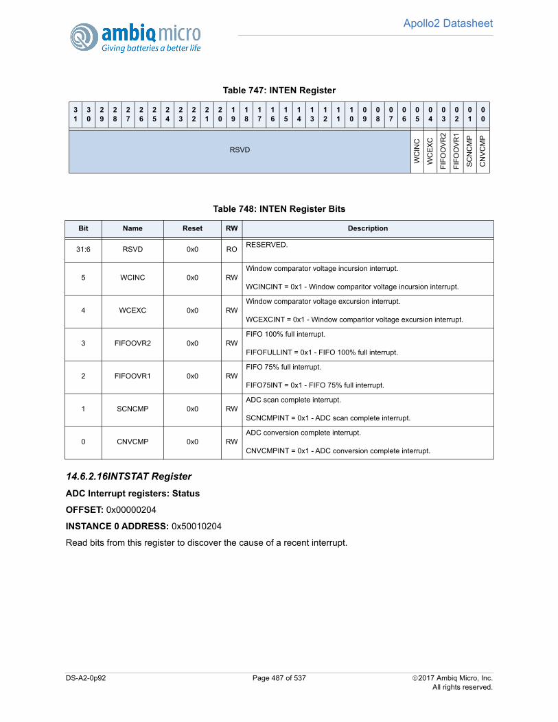
Apollo2 Datasheet
14.6.2.16INTSTAT Register
ADC Interrupt registers: Status
OFFSET: 0x00000204
INSTANCE 0 ADDRESS: 0x50010204
Read bits from this register to discover the cause of a recent interrupt.
Table 747: INTEN Register
31
30
29
28
27
26
25
24
23
22
21
20
19
18
17
16
15
14
13
12
11
10
09
08
07
06
05
04
03
02
01
00
RSVD
WC
INC
WC
EX
C
FIF
OO
VR
2
FIF
OO
VR
1
SC
NC
MP
CN
VC
MP
Table 748: INTEN Register Bits
Bit Name Reset RW Description
31:6 RSVD 0x0 RORESERVED.
5 WCINC 0x0 RWWindow comparator voltage incursion interrupt.
WCINCINT = 0x1 - Window comparitor voltage incursion interrupt.
4 WCEXC 0x0 RWWindow comparator voltage excursion interrupt.
WCEXCINT = 0x1 - Window comparitor voltage excursion interrupt.
3 FIFOOVR2 0x0 RWFIFO 100% full interrupt.
FIFOFULLINT = 0x1 - FIFO 100% full interrupt.
2 FIFOOVR1 0x0 RWFIFO 75% full interrupt.
FIFO75INT = 0x1 - FIFO 75% full interrupt.
1 SCNCMP 0x0 RWADC scan complete interrupt.
SCNCMPINT = 0x1 - ADC scan complete interrupt.
0 CNVCMP 0x0 RWADC conversion complete interrupt.
CNVCMPINT = 0x1 - ADC conversion complete interrupt.
DS-A2-0p92 Page 487 of 537 2017 Ambiq Micro, Inc.All rights reserved.
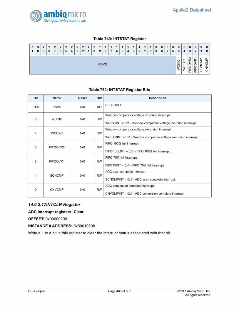
Apollo2 Datasheet
14.6.2.17INTCLR Register
ADC Interrupt registers: Clear
OFFSET: 0x00000208
INSTANCE 0 ADDRESS: 0x50010208
Write a 1 to a bit in this register to clear the interrupt status associated with that bit.
Table 749: INTSTAT Register
31
30
29
28
27
26
25
24
23
22
21
20
19
18
17
16
15
14
13
12
11
10
09
08
07
06
05
04
03
02
01
00
RSVD
WC
INC
WC
EX
C
FIF
OO
VR
2
FIF
OO
VR
1
SC
NC
MP
CN
VC
MP
Table 750: INTSTAT Register Bits
Bit Name Reset RW Description
31:6 RSVD 0x0 RORESERVED.
5 WCINC 0x0 RWWindow comparator voltage incursion interrupt.
WCINCINT = 0x1 - Window comparitor voltage incursion interrupt.
4 WCEXC 0x0 RWWindow comparator voltage excursion interrupt.
WCEXCINT = 0x1 - Window comparitor voltage excursion interrupt.
3 FIFOOVR2 0x0 RWFIFO 100% full interrupt.
FIFOFULLINT = 0x1 - FIFO 100% full interrupt.
2 FIFOOVR1 0x0 RWFIFO 75% full interrupt.
FIFO75INT = 0x1 - FIFO 75% full interrupt.
1 SCNCMP 0x0 RWADC scan complete interrupt.
SCNCMPINT = 0x1 - ADC scan complete interrupt.
0 CNVCMP 0x0 RWADC conversion complete interrupt.
CNVCMPINT = 0x1 - ADC conversion complete interrupt.
DS-A2-0p92 Page 488 of 537 2017 Ambiq Micro, Inc.All rights reserved.
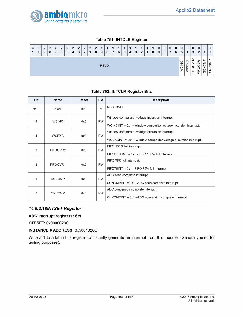
Apollo2 Datasheet
14.6.2.18INTSET Register
ADC Interrupt registers: Set
OFFSET: 0x0000020C
INSTANCE 0 ADDRESS: 0x5001020C
Write a 1 to a bit in this register to instantly generate an interrupt from this module. (Generally used fortesting purposes).
Table 751: INTCLR Register
31
30
29
28
27
26
25
24
23
22
21
20
19
18
17
16
15
14
13
12
11
10
09
08
07
06
05
04
03
02
01
00
RSVD
WC
INC
WC
EX
C
FIF
OO
VR
2
FIF
OO
VR
1
SC
NC
MP
CN
VC
MP
Table 752: INTCLR Register Bits
Bit Name Reset RW Description
31:6 RSVD 0x0 RORESERVED.
5 WCINC 0x0 RWWindow comparator voltage incursion interrupt.
WCINCINT = 0x1 - Window comparitor voltage incursion interrupt.
4 WCEXC 0x0 RWWindow comparator voltage excursion interrupt.
WCEXCINT = 0x1 - Window comparitor voltage excursion interrupt.
3 FIFOOVR2 0x0 RWFIFO 100% full interrupt.
FIFOFULLINT = 0x1 - FIFO 100% full interrupt.
2 FIFOOVR1 0x0 RWFIFO 75% full interrupt.
FIFO75INT = 0x1 - FIFO 75% full interrupt.
1 SCNCMP 0x0 RWADC scan complete interrupt.
SCNCMPINT = 0x1 - ADC scan complete interrupt.
0 CNVCMP 0x0 RWADC conversion complete interrupt.
CNVCMPINT = 0x1 - ADC conversion complete interrupt.
DS-A2-0p92 Page 489 of 537 2017 Ambiq Micro, Inc.All rights reserved.
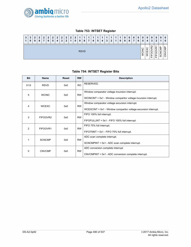
Apollo2 Datasheet
Table 753: INTSET Register
31
30
29
28
27
26
25
24
23
22
21
20
19
18
17
16
15
14
13
12
11
10
09
08
07
06
05
04
03
02
01
00
RSVD
WC
INC
WC
EX
C
FIF
OO
VR
2
FIF
OO
VR
1
SC
NC
MP
CN
VC
MP
Table 754: INTSET Register Bits
Bit Name Reset RW Description
31:6 RSVD 0x0 RORESERVED.
5 WCINC 0x0 RWWindow comparator voltage incursion interrupt.
WCINCINT = 0x1 - Window comparitor voltage incursion interrupt.
4 WCEXC 0x0 RWWindow comparator voltage excursion interrupt.
WCEXCINT = 0x1 - Window comparitor voltage excursion interrupt.
3 FIFOOVR2 0x0 RWFIFO 100% full interrupt.
FIFOFULLINT = 0x1 - FIFO 100% full interrupt.
2 FIFOOVR1 0x0 RWFIFO 75% full interrupt.
FIFO75INT = 0x1 - FIFO 75% full interrupt.
1 SCNCMP 0x0 RWADC scan complete interrupt.
SCNCMPINT = 0x1 - ADC scan complete interrupt.
0 CNVCMP 0x0 RWADC conversion complete interrupt.
CNVCMPINT = 0x1 - ADC conversion complete interrupt.
DS-A2-0p92 Page 490 of 537 2017 Ambiq Micro, Inc.All rights reserved.
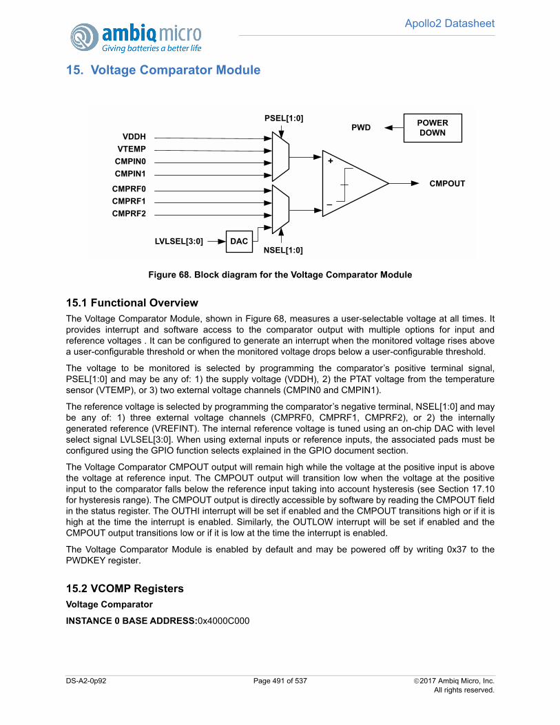
Apollo2 Datasheet
15. Voltage Comparator Module
Figure 68. Block diagram for the Voltage Comparator Module
15.1 Functional OverviewThe Voltage Comparator Module, shown in Figure 68, measures a user-selectable voltage at all times. Itprovides interrupt and software access to the comparator output with multiple options for input andreference voltages . It can be configured to generate an interrupt when the monitored voltage rises abovea user-configurable threshold or when the monitored voltage drops below a user-configurable threshold.
The voltage to be monitored is selected by programming the comparator’s positive terminal signal,PSEL[1:0] and may be any of: 1) the supply voltage (VDDH), 2) the PTAT voltage from the temperaturesensor (VTEMP), or 3) two external voltage channels (CMPIN0 and CMPIN1).
The reference voltage is selected by programming the comparator’s negative terminal, NSEL[1:0] and maybe any of: 1) three external voltage channels (CMPRF0, CMPRF1, CMPRF2), or 2) the internallygenerated reference (VREFINT). The internal reference voltage is tuned using an on-chip DAC with levelselect signal LVLSEL[3:0]. When using external inputs or reference inputs, the associated pads must beconfigured using the GPIO function selects explained in the GPIO document section.
The Voltage Comparator CMPOUT output will remain high while the voltage at the positive input is abovethe voltage at reference input. The CMPOUT output will transition low when the voltage at the positiveinput to the comparator falls below the reference input taking into account hysteresis (see Section 17.10for hysteresis range). The CMPOUT output is directly accessible by software by reading the CMPOUT fieldin the status register. The OUTHI interrupt will be set if enabled and the CMPOUT transitions high or if it ishigh at the time the interrupt is enabled. Similarly, the OUTLOW interrupt will be set if enabled and theCMPOUT output transitions low or if it is low at the time the interrupt is enabled.
The Voltage Comparator Module is enabled by default and may be powered off by writing 0x37 to thePWDKEY register.
15.2 VCOMP RegistersVoltage Comparator
INSTANCE 0 BASE ADDRESS:0x4000C000
VDDH
DAC
VTEMPCMPIN0CMPIN1
CMPRF0CMPRF1CMPRF2
PSEL[1:0]
+
_
LVLSEL[3:0]NSEL[1:0]
CMPOUT
POWER DOWNPWD
DS-A2-0p92 Page 491 of 537 2017 Ambiq Micro, Inc.All rights reserved.

Apollo2 Datasheet
This is the detailed description of the Voltage Comparator Register Block. The Voltage Cmparator RegisterBlock contains the software control for selecting the comparator inputs, powerdown control, observingcomparator output status and enabling interrupts.
15.2.1 Register Memory Map
Table 755: VCOMP Register Map
Address(s) Register Name Description
0x4000C000 CFG Configuration Register
0x4000C004 STAT Status Register
0x4000C008 PWDKEYKey Register for Powering Down the VoltageComparator
0x4000C200 INTEN Voltage Comparator Interrupt registers: Enable
0x4000C204 INTSTAT Voltage Comparator Interrupt registers: Status
0x4000C208 INTCLR Voltage Comparator Interrupt registers: Clear
0x4000C20C INTSET Voltage Comparator Interrupt registers: Set
DS-A2-0p92 Page 492 of 537 2017 Ambiq Micro, Inc.All rights reserved.

Apollo2 Datasheet
15.2.2 VCOMP Registers
15.2.2.1 CFG Register
Configuration Register
OFFSET: 0x00000000
INSTANCE 0 ADDRESS: 0x4000C000
The Voltage Comparator Configuration Register contains the software control for selecting beween the 4options for the positive input as well as the multiple options for the reference input.
Table 756: CFG Register
31
30
29
28
27
26
25
24
23
22
21
20
19
18
17
16
15
14
13
12
11
10
09
08
07
06
05
04
03
02
01
00
RSVD LVLSEL RSVD
NS
EL
RSVD
PS
EL
Table 757: CFG Register Bits
Bit Name Reset RW Description
31:20 RSVD 0x0 ROThis bitfield is reserved for future use.
19:16 LVLSEL 0x0 RW
When the reference input NSEL is set to NSEL_DAC, this bitfield selects thevoltage level for the negative input to the comparator.
0P58V = 0x0 - Set Reference input to 0.58 Volts.0P77V = 0x1 - Set Reference input to 0.77 Volts.0P97V = 0x2 - Set Reference input to 0.97 Volts.1P16V = 0x3 - Set Reference input to 1.16 Volts.1P35V = 0x4 - Set Reference input to 1.35 Volts.1P55V = 0x5 - Set Reference input to 1.55 Volts.1P74V = 0x6 - Set Reference input to 1.74 Volts.1P93V = 0x7 - Set Reference input to 1.93 Volts.2P13V = 0x8 - Set Reference input to 2.13 Volts.2P32V = 0x9 - Set Reference input to 2.32 Volts.2P51V = 0xA - Set Reference input to 2.51 Volts.2P71V = 0xB - Set Reference input to 2.71 Volts.2P90V = 0xC - Set Reference input to 2.90 Volts.3P09V = 0xD - Set Reference input to 3.09 Volts.3P29V = 0xE - Set Reference input to 3.29 Volts.3P48V = 0xF - Set Reference input to 3.48 Volts.
15:10 RSVD 0x0 ROThis bitfield is reserved for future use.
9:8 NSEL 0x0 RW
This bitfield selects the negative input to the comparator.
VREFEXT1 = 0x0 - Use external reference 1 for reference input.VREFEXT2 = 0x1 - Use external reference 2 for reference input.VREFEXT3 = 0x2 - Use external reference 3 for reference input.DAC = 0x3 - Use DAC output selected by LVLSEL for reference input.
7:2 RSVD 0x0 ROThis bitfield is reserved for future use.
DS-A2-0p92 Page 493 of 537 2017 Ambiq Micro, Inc.All rights reserved.
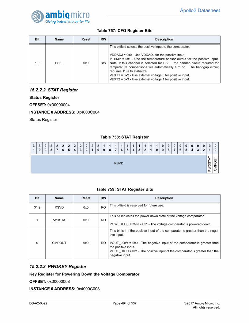
Apollo2 Datasheet
15.2.2.2 STAT Register
Status Register
OFFSET: 0x00000004
INSTANCE 0 ADDRESS: 0x4000C004
Status Register
15.2.2.3 PWDKEY Register
Key Register for Powering Down the Voltage Comparator
OFFSET: 0x00000008
INSTANCE 0 ADDRESS: 0x4000C008
1:0 PSEL 0x0 RW
This bitfield selects the positive input to the comparator.
VDDADJ = 0x0 - Use VDDADJ for the positive input.VTEMP = 0x1 - Use the temperature sensor output for the positive input.Note: If this channel is selected for PSEL, the bandap circuit required fortemperature comparisons will automatically turn on. The bandgap circuitrequires 11us to stabalize.VEXT1 = 0x2 - Use external voltage 0 for positive input.VEXT2 = 0x3 - Use external voltage 1 for positive input.
Table 758: STAT Register
31
30
29
28
27
26
25
24
23
22
21
20
19
18
17
16
15
14
13
12
11
10
09
08
07
06
05
04
03
02
01
00
RSVD
PW
DS
TAT
CM
PO
UT
Table 759: STAT Register Bits
Bit Name Reset RW Description
31:2 RSVD 0x0 ROThis bitfield is reserved for future use.
1 PWDSTAT 0x0 ROThis bit indicates the power down state of the voltage comparator.
POWERED_DOWN = 0x1 - The voltage comparator is powered down.
0 CMPOUT 0x0 RO
This bit is 1 if the positive input of the comparator is greater than the nega-tive input.
VOUT_LOW = 0x0 - The negative input of the comparator is greater thanthe positive input.VOUT_HIGH = 0x1 - The positive input of the comparator is greater than thenegative input.
Table 757: CFG Register Bits
Bit Name Reset RW Description
DS-A2-0p92 Page 494 of 537 2017 Ambiq Micro, Inc.All rights reserved.
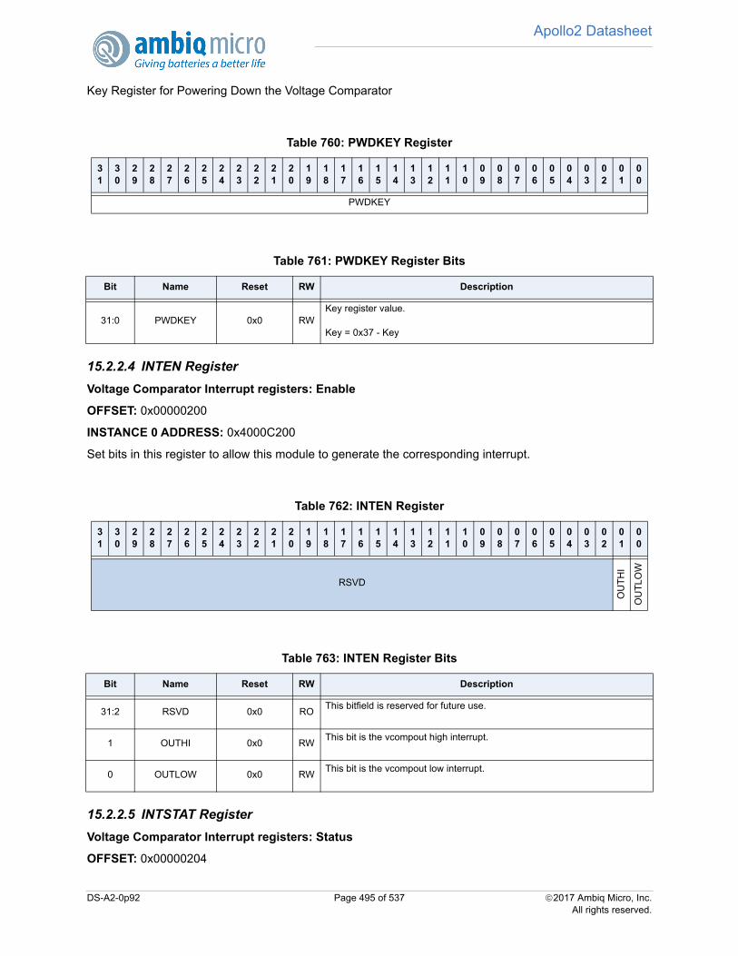
Apollo2 Datasheet
Key Register for Powering Down the Voltage Comparator
15.2.2.4 INTEN Register
Voltage Comparator Interrupt registers: Enable
OFFSET: 0x00000200
INSTANCE 0 ADDRESS: 0x4000C200
Set bits in this register to allow this module to generate the corresponding interrupt.
15.2.2.5 INTSTAT Register
Voltage Comparator Interrupt registers: Status
OFFSET: 0x00000204
Table 760: PWDKEY Register
31
30
29
28
27
26
25
24
23
22
21
20
19
18
17
16
15
14
13
12
11
10
09
08
07
06
05
04
03
02
01
00
PWDKEY
Table 761: PWDKEY Register Bits
Bit Name Reset RW Description
31:0 PWDKEY 0x0 RWKey register value.
Key = 0x37 - Key
Table 762: INTEN Register
31
30
29
28
27
26
25
24
23
22
21
20
19
18
17
16
15
14
13
12
11
10
09
08
07
06
05
04
03
02
01
00
RSVD
OU
TH
I
OU
TLO
W
Table 763: INTEN Register Bits
Bit Name Reset RW Description
31:2 RSVD 0x0 ROThis bitfield is reserved for future use.
1 OUTHI 0x0 RWThis bit is the vcompout high interrupt.
0 OUTLOW 0x0 RWThis bit is the vcompout low interrupt.
DS-A2-0p92 Page 495 of 537 2017 Ambiq Micro, Inc.All rights reserved.
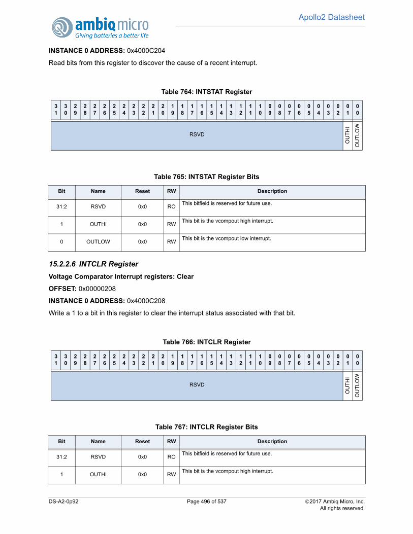
Apollo2 Datasheet
INSTANCE 0 ADDRESS: 0x4000C204
Read bits from this register to discover the cause of a recent interrupt.
15.2.2.6 INTCLR Register
Voltage Comparator Interrupt registers: Clear
OFFSET: 0x00000208
INSTANCE 0 ADDRESS: 0x4000C208
Write a 1 to a bit in this register to clear the interrupt status associated with that bit.
Table 764: INTSTAT Register
31
30
29
28
27
26
25
24
23
22
21
20
19
18
17
16
15
14
13
12
11
10
09
08
07
06
05
04
03
02
01
00
RSVD
OU
TH
I
OU
TLO
W
Table 765: INTSTAT Register Bits
Bit Name Reset RW Description
31:2 RSVD 0x0 ROThis bitfield is reserved for future use.
1 OUTHI 0x0 RWThis bit is the vcompout high interrupt.
0 OUTLOW 0x0 RWThis bit is the vcompout low interrupt.
Table 766: INTCLR Register
31
30
29
28
27
26
25
24
23
22
21
20
19
18
17
16
15
14
13
12
11
10
09
08
07
06
05
04
03
02
01
00
RSVD
OU
TH
I
OU
TL
OW
Table 767: INTCLR Register Bits
Bit Name Reset RW Description
31:2 RSVD 0x0 ROThis bitfield is reserved for future use.
1 OUTHI 0x0 RWThis bit is the vcompout high interrupt.
DS-A2-0p92 Page 496 of 537 2017 Ambiq Micro, Inc.All rights reserved.
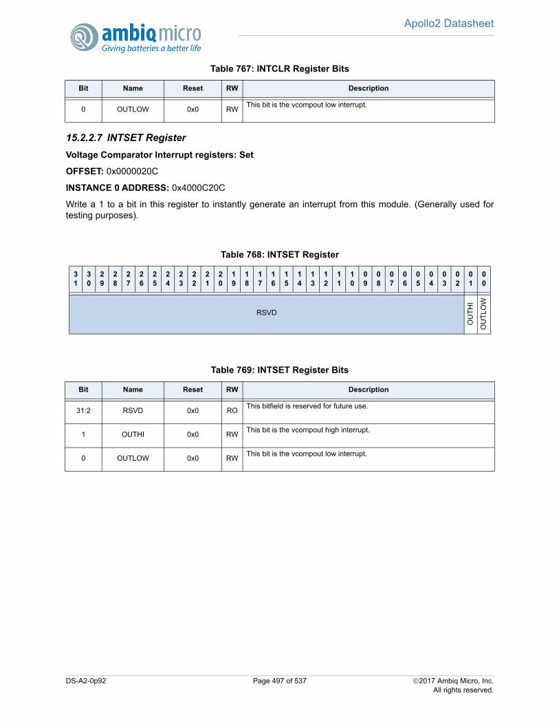
Apollo2 Datasheet
15.2.2.7 INTSET Register
Voltage Comparator Interrupt registers: Set
OFFSET: 0x0000020C
INSTANCE 0 ADDRESS: 0x4000C20C
Write a 1 to a bit in this register to instantly generate an interrupt from this module. (Generally used fortesting purposes).
0 OUTLOW 0x0 RWThis bit is the vcompout low interrupt.
Table 768: INTSET Register
31
30
29
28
27
26
25
24
23
22
21
20
19
18
17
16
15
14
13
12
11
10
09
08
07
06
05
04
03
02
01
00
RSVD
OU
TH
I
OU
TLO
W
Table 769: INTSET Register Bits
Bit Name Reset RW Description
31:2 RSVD 0x0 ROThis bitfield is reserved for future use.
1 OUTHI 0x0 RWThis bit is the vcompout high interrupt.
0 OUTLOW 0x0 RWThis bit is the vcompout low interrupt.
Table 767: INTCLR Register Bits
Bit Name Reset RW Description
DS-A2-0p92 Page 497 of 537 2017 Ambiq Micro, Inc.All rights reserved.

Apollo2 Datasheet
16. Voltage Regulator Module
Figure 69. Block Diagram for the Voltage Regulator Module
16.1 Functional OverviewThe Voltage Regulator Module down-converts and regulates the supply voltage, VDD, with extremely highefficiency. A pair of Buck Converters enables down-conversion from the power supply input (e.g., abattery) at efficiency of >90%. With ultra-low quiescent current, the Buck Converters are optimized for lowpower environments. There are also integrated low dropout linear regulators which are used in very lowpower modes and can also be utilized to provide a lower cost system solution by eliminating the need forthe external capacitors/inductors required in buck mode.
The Buck Converters and LDOs of the Voltage Regulator Module are tightly coupled to the various lowpower modes in the Apollo2 MCU. When the Apollo2 MCU enters deep sleep mode, the Buck Converterscan be optionally powered down and bypassed, and the LDOs can be placed in an extreme low powermode with only nanoamps of quiescent current.
LDO
Buck Converter 1
LDO
Buck Converter 2
LDO
VDD
To Core
To Logic
To Analog Blocks
To Memory
DS-A2-0p92 Page 498 of 537 2017 Ambiq Micro, Inc.All rights reserved.
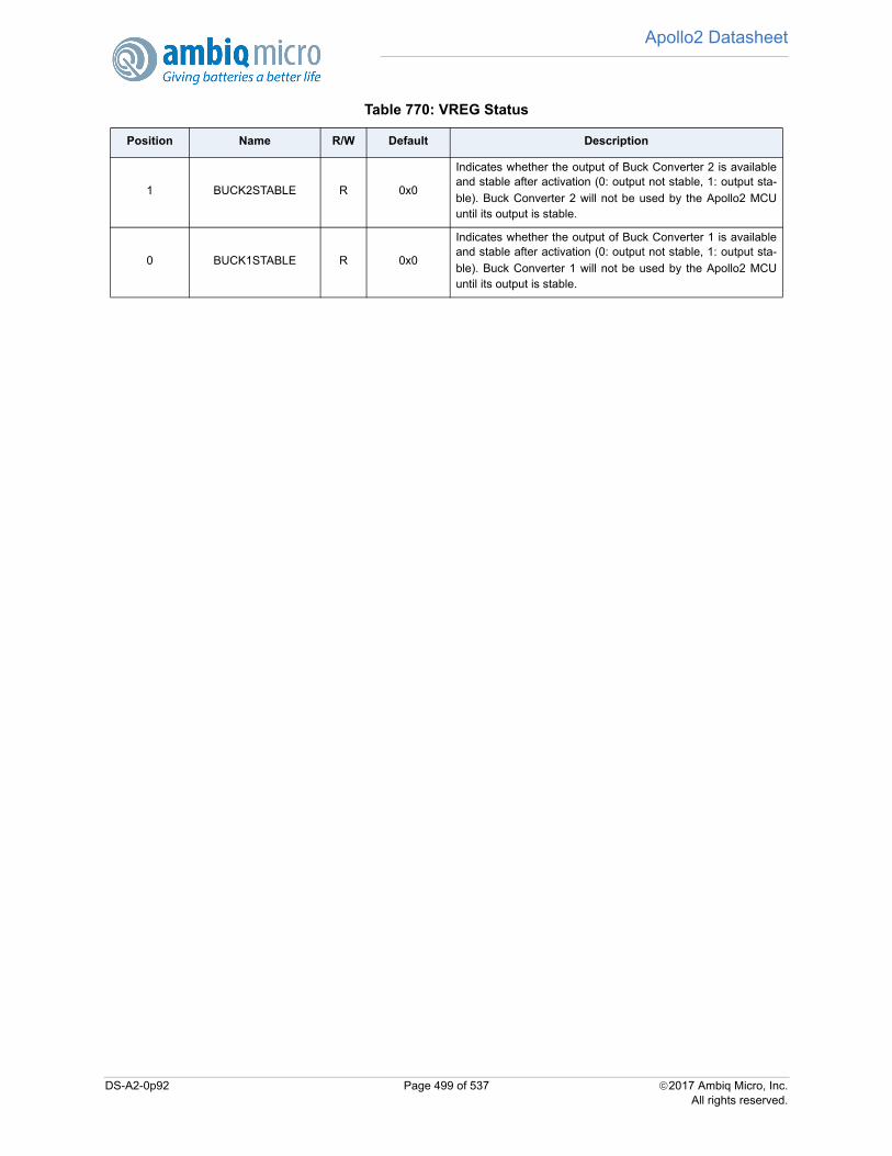
Apollo2 Datasheet
Table 770: VREG Status
Position Name R/W Default Description
1 BUCK2STABLE R 0x0
Indicates whether the output of Buck Converter 2 is availableand stable after activation (0: output not stable, 1: output sta-
ble). Buck Converter 2 will not be used by the Apollo2 MCUuntil its output is stable.
0 BUCK1STABLE R 0x0
Indicates whether the output of Buck Converter 1 is availableand stable after activation (0: output not stable, 1: output sta-
ble). Buck Converter 1 will not be used by the Apollo2 MCUuntil its output is stable.
DS-A2-0p92 Page 499 of 537 2017 Ambiq Micro, Inc.All rights reserved.
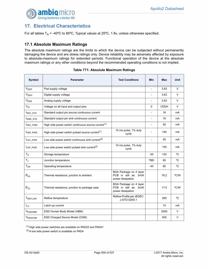
Apollo2 Datasheet
17. Electrical Characteristics
For all tables TA = -40ºC to 85ºC, Typical values at 25ºC, 1.8v, unless otherwise specified.
17.1 Absolute Maximum RatingsThe absolute maximum ratings are the limits to which the device can be subjected without permanentlydamaging the device and are stress ratings only. Device reliability may be adversely affected by exposureto absolute-maximum ratings for extended periods. Functional operation of the device at the absolutemaximum ratings or any other conditions beyond the recommended operating conditions is not implied.
(1) High side power switches are available on PAD22 and PAD41(2) A low side power switch is available on PAD4
Table 771: Absolute Maximum Ratings
Symbol Parameter Test Conditions Min Max Unit
VDDP Pad supply voltage - 3.63 V
VDDH Digital supply voltage - 3.63 V
VDDA Analog supply voltage - 3.63 V
VIO Voltage on all input and output pins 0 VDDH V
ISRC_STD Standard output pin source continuous current - 16 mA
ISINK_STD Standard output pin sink continuous current - 16 mA
IHSC_PWR High side power switch continuous source current(1) - 50 mA
IHSP_PWR High side power switch pulsed source current(1) 10 ms pulse, 1% duty cycle
- 150 mA
ILSC_PWR Low side power switch continuous sink current(2) - 50 mA
ILSP_PWR Low side power switch pulsed sink current(2) 10 ms pulse, 1% duty cycle
150 mA
TS Storage temperature -55 125 ºC
TJ Junction temperature TBD 85 ºC
TOP Operating temperature -40 85 ºC
JA Thermal resistance, junction to ambientBGA Package on 4 layerPCB in still air, 3mWpower dissipation
76.2 ºC/W
JC Thermal resistance, junction to package caseBGA Package on 4 layerPCB in still air, 3mWpower dissipation
17.0 ºC/W
TREFLOW Reflow temperatureReflow Profile per JEDEC
J-STD-020D.1260 ºC
ILU Latch-up current 10 mA
VESDHBM ESD Human Body Model (HBM) 2500 V
VESDCDM ESD Charged Device Model (CDM) 500 V
DS-A2-0p92 Page 500 of 537 2017 Ambiq Micro, Inc.All rights reserved.
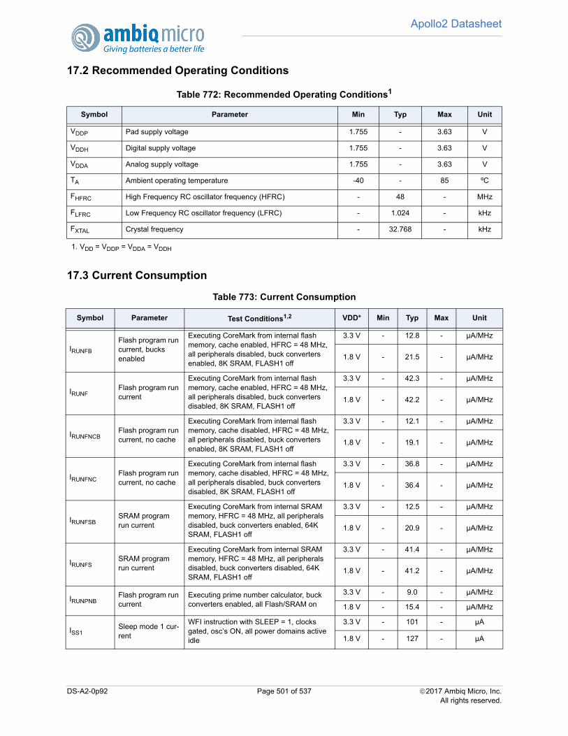
Apollo2 Datasheet
17.2 Recommended Operating Conditions
17.3 Current Consumption
Table 772: Recommended Operating Conditions1
1. VDD = VDDP = VDDA = VDDH
Symbol Parameter Min Typ Max Unit
VDDP Pad supply voltage 1.755 - 3.63 V
VDDH Digital supply voltage 1.755 - 3.63 V
VDDA Analog supply voltage 1.755 - 3.63 V
TA Ambient operating temperature -40 - 85 ºC
FHFRC High Frequency RC oscillator frequency (HFRC) - 48 - MHz
FLFRC Low Frequency RC oscillator frequency (LFRC) - 1.024 - kHz
FXTAL Crystal frequency - 32.768 - kHz
Table 773: Current Consumption
Symbol Parameter Test Conditions1,2 VDD* Min Typ Max Unit
IRUNFB
Flash program run current, bucks enabled
Executing CoreMark from internal flash memory, cache enabled, HFRC = 48 MHz, all peripherals disabled, buck converters enabled, 8K SRAM, FLASH1 off
3.3 V - 12.8 - µA/MHz
1.8 V - 21.5 - µA/MHz
IRUNFFlash program run current
Executing CoreMark from internal flash memory, cache enabled, HFRC = 48 MHz, all peripherals disabled, buck converters disabled, 8K SRAM, FLASH1 off
3.3 V - 42.3 - µA/MHz
1.8 V - 42.2 - µA/MHz
IRUNFNCBFlash program run current, no cache
Executing CoreMark from internal flash memory, cache disabled, HFRC = 48 MHz, all peripherals disabled, buck converters enabled, 8K SRAM, FLASH1 off
3.3 V - 12.1 - µA/MHz
1.8 V - 19.1 - µA/MHz
IRUNFNCFlash program run current, no cache
Executing CoreMark from internal flash memory, cache disabled, HFRC = 48 MHz, all peripherals disabled, buck converters disabled, 8K SRAM, FLASH1 off
3.3 V - 36.8 - µA/MHz
1.8 V - 36.4 - µA/MHz
IRUNFSBSRAM program run current
Executing CoreMark from internal SRAM memory, HFRC = 48 MHz, all peripherals disabled, buck converters enabled, 64K SRAM, FLASH1 off
3.3 V - 12.5 - µA/MHz
1.8 V - 20.9 - µA/MHz
IRUNFSSRAM program run current
Executing CoreMark from internal SRAM memory, HFRC = 48 MHz, all peripherals disabled, buck converters disabled, 64K SRAM, FLASH1 off
3.3 V - 41.4 - µA/MHz
1.8 V - 41.2 - µA/MHz
IRUNPNBFlash program run current
Executing prime number calculator, buck converters enabled, all Flash/SRAM on
3.3 V - 9.0 - µA/MHz
1.8 V - 15.4 - µA/MHz
ISS1Sleep mode 1 cur-rent
WFI instruction with SLEEP = 1, clocks gated, osc’s ON, all power domains active idle
3.3 V - 101 - µA
1.8 V - 127 - µA
DS-A2-0p92 Page 501 of 537 2017 Ambiq Micro, Inc.All rights reserved.
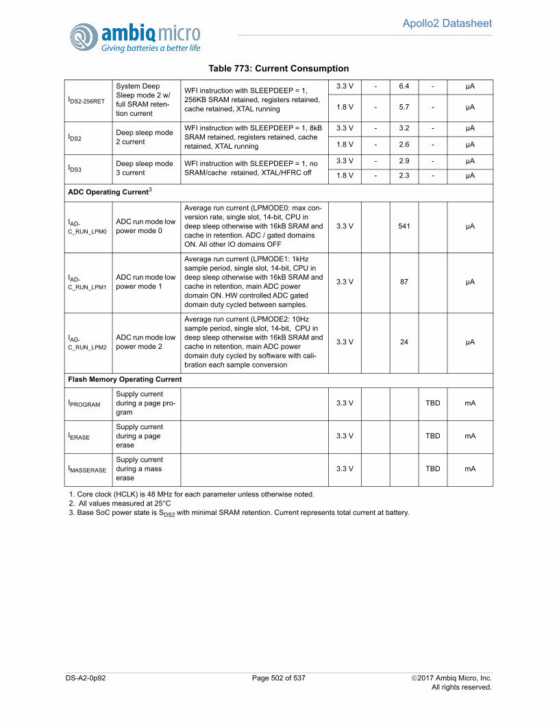
Apollo2 Datasheet
IDS2-256RET
System Deep Sleep mode 2 w/full SRAM reten-tion current
WFI instruction with SLEEPDEEP = 1, 256KB SRAM retained, registers retained, cache retained, XTAL running
3.3 V - 6.4 - µA
1.8 V - 5.7 - µA
IDS2Deep sleep mode 2 current
WFI instruction with SLEEPDEEP = 1, 8kB SRAM retained, registers retained, cache retained, XTAL running
3.3 V - 3.2 - µA
1.8 V - 2.6 - µA
IDS3Deep sleep mode 3 current
WFI instruction with SLEEPDEEP = 1, no SRAM/cache retained, XTAL/HFRC off
3.3 V - 2.9 - µA
1.8 V - 2.3 - µA
ADC Operating Current3
IAD-C_RUN_LPM0
ADC run mode low power mode 0
Average run current (LPMODE0: max con-version rate, single slot, 14-bit, CPU in deep sleep otherwise with 16kB SRAM and cache in retention. ADC / gated domains ON. All other IO domains OFF
3.3 V 541 µA
IAD-C_RUN_LPM1
ADC run mode low power mode 1
Average run current (LPMODE1: 1kHz sample period, single slot, 14-bit, CPU in deep sleep otherwise with 16kB SRAM and cache in retention, main ADC power domain ON. HW controlled ADC gated domain duty cycled between samples.
3.3 V 87 µA
IAD-C_RUN_LPM2
ADC run mode low power mode 2
Average run current (LPMODE2: 10Hz sample period, single slot, 14-bit, CPU in deep sleep otherwise with 16kB SRAM and cache in retention, main ADC power domain duty cycled by software with cali-bration each sample conversion
3.3 V 24 µA
Flash Memory Operating Current
IPROGRAM
Supply current during a page pro-gram
3.3 V TBD mA
IERASE
Supply current during a page erase
3.3 V TBD mA
IMASSERASE Supply current during a mass erase
3.3 V TBD mA
1. Core clock (HCLK) is 48 MHz for each parameter unless otherwise noted.2. All values measured at 25°C3. Base SoC power state is SDS2 with minimal SRAM retention. Current represents total current at battery.
Table 773: Current Consumption
DS-A2-0p92 Page 502 of 537 2017 Ambiq Micro, Inc.All rights reserved.
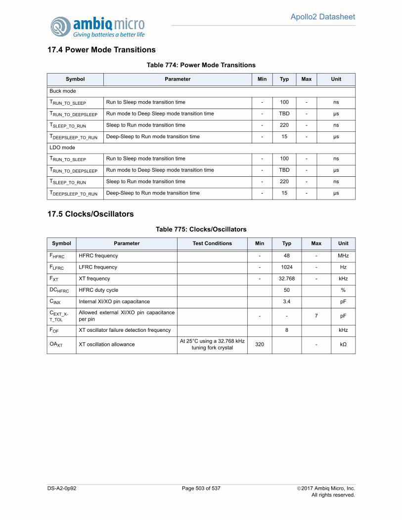
Apollo2 Datasheet
17.4 Power Mode Transitions
17.5 Clocks/Oscillators
Table 774: Power Mode Transitions
Symbol Parameter Min Typ Max Unit
Buck mode
TRUN_TO_SLEEP Run to Sleep mode transition time - 100 - ns
TRUN_TO_DEEPSLEEP Run mode to Deep Sleep mode transition time - TBD - µs
TSLEEP_TO_RUN Sleep to Run mode transition time - 220 - ns
TDEEPSLEEP_TO_RUN Deep-Sleep to Run mode transition time - 15 - µs
LDO mode
TRUN_TO_SLEEP Run to Sleep mode transition time - 100 - ns
TRUN_TO_DEEPSLEEP Run mode to Deep Sleep mode transition time - TBD - µs
TSLEEP_TO_RUN Sleep to Run mode transition time - 220 - ns
TDEEPSLEEP_TO_RUN Deep-Sleep to Run mode transition time - 15 - µs
Table 775: Clocks/Oscillators
Symbol Parameter Test Conditions Min Typ Max Unit
FHFRC HFRC frequency - 48 - MHz
FLFRC LFRC frequency - 1024 - Hz
FXT XT frequency - 32.768 - kHz
DCHFRC HFRC duty cycle 50 %
CINX Internal XI/XO pin capacitance 3.4 pF
CEXT_X-T_TOL
Allowed external XI/XO pin capacitanceper pin
- - 7 pF
FOF XT oscillator failure detection frequency 8 kHz
OAXT XT oscillation allowanceAt 25°C using a 32.768 kHz
tuning fork crystal320 - kΩ
DS-A2-0p92 Page 503 of 537 2017 Ambiq Micro, Inc.All rights reserved.

Apollo2 Datasheet
17.6 Analog-to-Digital Converter (ADC)
Table 776: Analog to Digital Converter (ADC)
Symbol ParameterTest
ConditionsMin Typ Max Unit
ANALOG INPUT
VADCIN Input voltage range single-ended input 0 VADCREF V
VADCIN_DIFF Input voltage range in differential mode-VADCREF/
2
+VAD-
CREF/2 V
VADCINN
VADCINPAbsolute differential input voltage range 0 VDDH V
VADCREF_15 Reference voltage range (1.5v mode) 1.425 1.5 1.575 V
VADCREF_20 Reference voltage range (2.0v mode) 1.9 2.0 2.1 V
IADCIN ADC channel pin input leakage current(static)
1 TBD pA
CADCIN Input source capacitance 4 pF
CADCVREFExternal ADC capacitance for internal ref-erence
400 470 540 nF
SAMPLING DYNAMICS
RES Resolution 8 14 bit
FADCONV Conversion rate
1.2 (14b)1.7(12b)2.4(10b)2.8 (8b)
MS/s
TTRIG_TO_START_L2
Delay from trigger to start of conversion –LPM2, Slot 0
TBD µs
TTRIG_TO_START_L1
Delay from trigger to start of conversion –LPM1, Slot 0, warm start
TBD µs
TTRIG_TO_START_L0
Delay from trigger to start of conversion –LPM0, Slot 0, warm start
TBD µs
TTRIG_TO_START_L1_CS
Delay from trigger to start of conversion –LPM1, Slot 0, cold start
TBD µs
TTRIG_TO_START_L0_CS
Delay from trigger to start of conversion –LPM0, Slot 0, cold start
TBD µs
TCAL Calibration Period 6415 cycles
DYNAMIC CHARACTERISTICS, Buck Disabled, 2v Reference
ENOBCAL Calibrated ENOB
LDO mode - Single/Diff.
Ended Input, external 2 V ref,
1 kHz input, ADC running in
14-bit mode
11.9 ENOB
DS-A2-0p92 Page 504 of 537 2017 Ambiq Micro, Inc.All rights reserved.
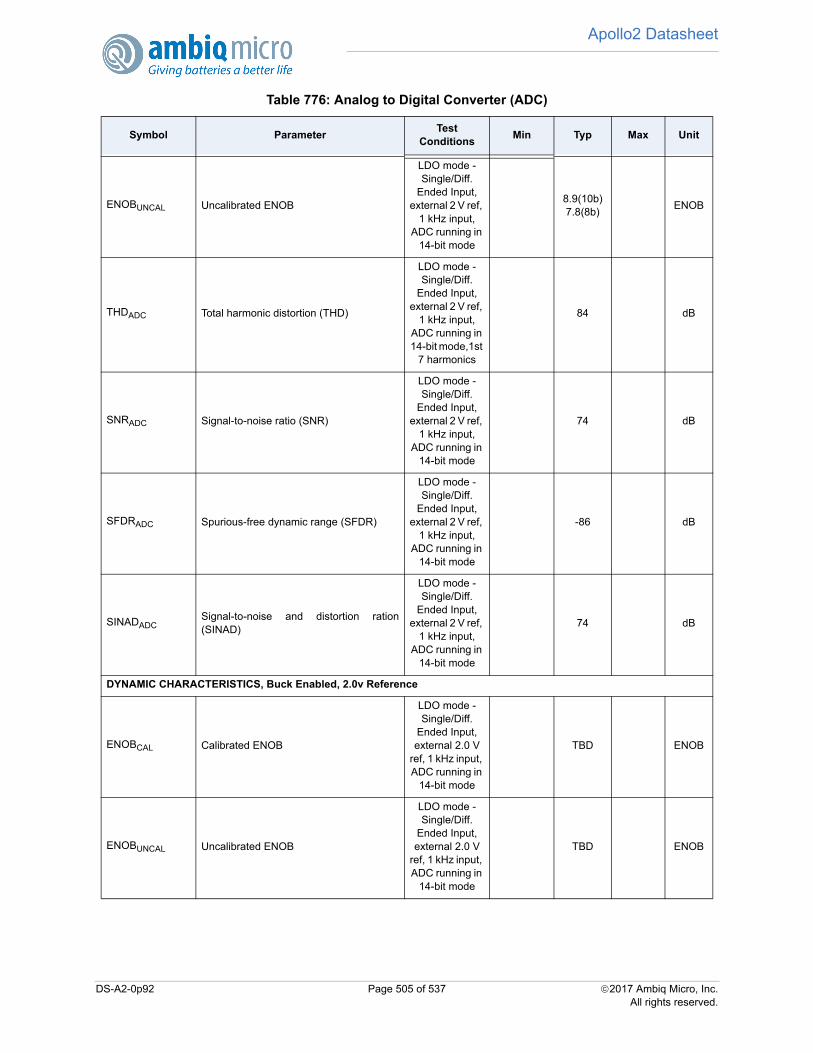
Apollo2 Datasheet
ENOBUNCAL Uncalibrated ENOB
LDO mode - Single/Diff.
Ended Input, external 2 V ref,
1 kHz input, ADC running in
14-bit mode
8.9(10b)7.8(8b)
ENOB
THDADC Total harmonic distortion (THD)
LDO mode - Single/Diff.
Ended Input, external 2 V ref,
1 kHz input, ADC running in 14-bit mode,1st
7 harmonics
84 dB
SNRADC Signal-to-noise ratio (SNR)
LDO mode - Single/Diff.
Ended Input, external 2 V ref,
1 kHz input, ADC running in
14-bit mode
74 dB
SFDRADC Spurious-free dynamic range (SFDR)
LDO mode - Single/Diff.
Ended Input, external 2 V ref,
1 kHz input, ADC running in
14-bit mode
-86 dB
SINADADCSignal-to-noise and distortion ration(SINAD)
LDO mode - Single/Diff.
Ended Input, external 2 V ref,
1 kHz input, ADC running in
14-bit mode
74 dB
DYNAMIC CHARACTERISTICS, Buck Enabled, 2.0v Reference
ENOBCAL Calibrated ENOB
LDO mode - Single/Diff.
Ended Input, external 2.0 V
ref, 1 kHz input, ADC running in
14-bit mode
TBD ENOB
ENOBUNCAL Uncalibrated ENOB
LDO mode - Single/Diff.
Ended Input, external 2.0 V
ref, 1 kHz input, ADC running in
14-bit mode
TBD ENOB
Table 776: Analog to Digital Converter (ADC)
Symbol ParameterTest
ConditionsMin Typ Max Unit
DS-A2-0p92 Page 505 of 537 2017 Ambiq Micro, Inc.All rights reserved.

Apollo2 Datasheet
THDADC Total harmonic distortion (THD)
LDO mode - Single/Diff.
Ended Input, external 2.0 V
ref, 1 kHz input, ADC running in 14-bit mode,1st
7 harmonics
TBD dB
SNRADC Signal-to-noise ratio (SNR)
LDO mode - Single/Diff.
Ended Input, external 2.0 V
ref, 1 kHz input, ADC running in
14-bit mode
TBD dB
SFDRADC Spurious-free dynamic range (SFDR)
LDO mode - Single/Diff.
Ended Input, external 2.0 V
ref, 1 kHz input, ADC running in
14-bit mode
TBD dB
SINADADCSignal-to-noise and distortion ration(SINAD)
LDO mode - Single/Diff.
Ended Input, external 2.0 V
ref, 1 kHz input, ADC running in
14-bit mode
TBD dB
PERFORMANCE
NMCADC No missing codes TBD bits
INLADC Integral nonlinearity Full input range +/- 2 LSB
DNLADC Differential nonlinearity Full input range +/- 0.9 LSB
EADC_OFFEST Offset error 1 1 %FS
EADC_GAIN Gain error 1 %FS
INTERNAL TEMPERATURE SENSOR
ETEMP Temperature sensor accuracy 3 °C
STEMP Temperature sensor slope 3.8 mV/°C
BATTERY RESISTANCE
RBATTInternal resistance for Battery Measure-ment
RBATT_INIT
- 7%
RBAT-T_INIT
RBAT-
T_INIT +
7%
Ω
VBATTDIV Battery divider voltage -2%0.333 * VDDH
+2% V
Table 776: Analog to Digital Converter (ADC)
Symbol ParameterTest
ConditionsMin Typ Max Unit
DS-A2-0p92 Page 506 of 537 2017 Ambiq Micro, Inc.All rights reserved.
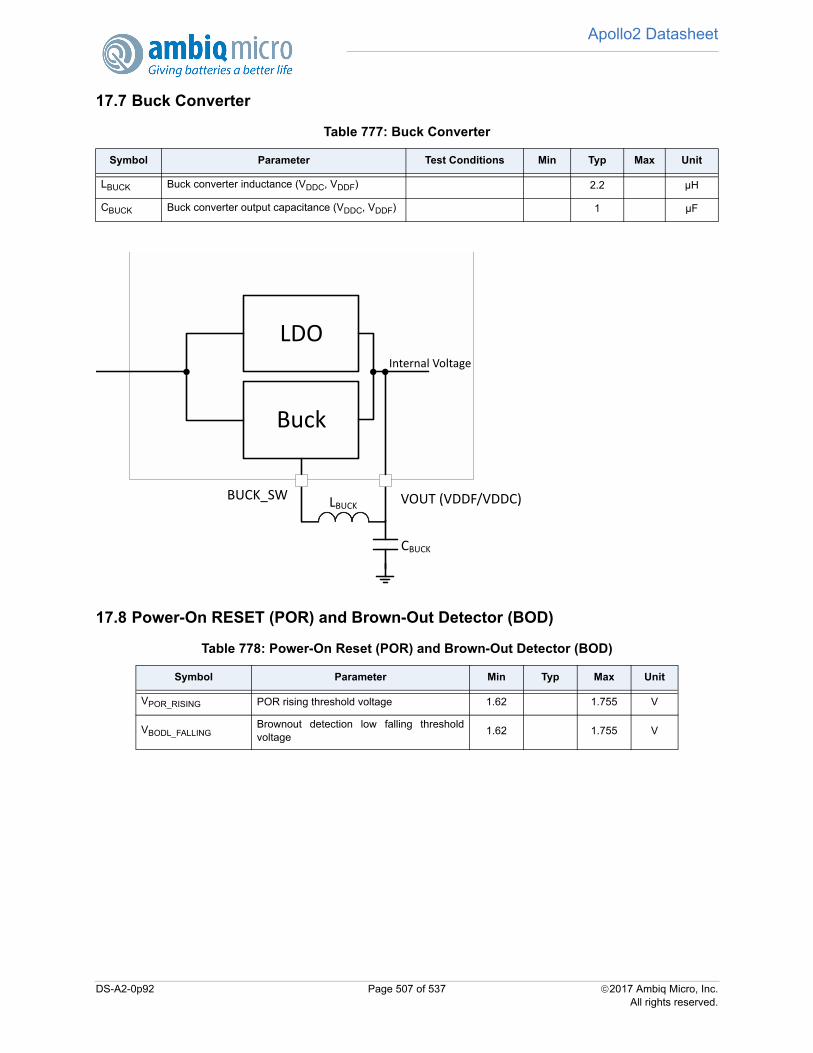
Apollo2 Datasheet
17.7 Buck Converter
17.8 Power-On RESET (POR) and Brown-Out Detector (BOD)
Table 777: Buck Converter
Symbol Parameter Test Conditions Min Typ Max Unit
LBUCK Buck converter inductance (VDDC, VDDF) 2.2 µH
CBUCK Buck converter output capacitance (VDDC, VDDF) 1 µF
Table 778: Power-On Reset (POR) and Brown-Out Detector (BOD)
Symbol Parameter Min Typ Max Unit
VPOR_RISING POR rising threshold voltage 1.62 1.755 V
VBODL_FALLINGBrownout detection low falling thresholdvoltage
1.62 1.755 V
Buck
LDOInternal Voltage
LBUCK
CBUCK
BUCK_SW VOUT (VDDF/VDDC)
DS-A2-0p92 Page 507 of 537 2017 Ambiq Micro, Inc.All rights reserved.
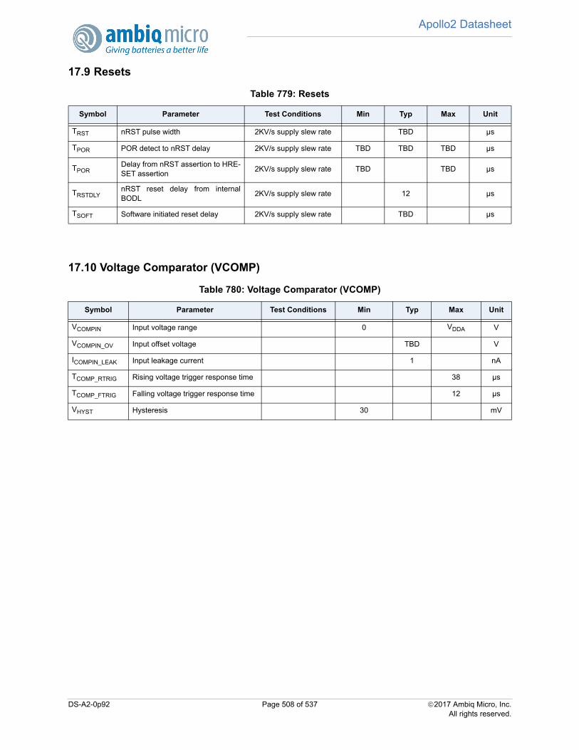
Apollo2 Datasheet
17.9 Resets
17.10 Voltage Comparator (VCOMP)
Table 779: Resets
Symbol Parameter Test Conditions Min Typ Max Unit
TRST nRST pulse width 2KV/s supply slew rate TBD µs
TPOR POR detect to nRST delay 2KV/s supply slew rate TBD TBD TBD µs
TPORDelay from nRST assertion to HRE-SET assertion
2KV/s supply slew rate TBD TBD µs
TRSTDLYnRST reset delay from internalBODL
2KV/s supply slew rate 12 µs
TSOFT Software initiated reset delay 2KV/s supply slew rate TBD µs
Table 780: Voltage Comparator (VCOMP)
Symbol Parameter Test Conditions Min Typ Max Unit
VCOMPIN Input voltage range 0 VDDA V
VCOMPIN_OV Input offset voltage TBD V
ICOMPIN_LEAK Input leakage current 1 nA
TCOMP_RTRIG Rising voltage trigger response time 38 µs
TCOMP_FTRIG Falling voltage trigger response time 12 µs
VHYST Hysteresis 30 mV
DS-A2-0p92 Page 508 of 537 2017 Ambiq Micro, Inc.All rights reserved.
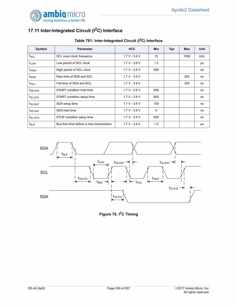
Apollo2 Datasheet
17.11 Inter-Integrated Circuit (I2C) Interface
Figure 70. I2C Timing
Table 781: Inter-Integrated Circuit (I2C) Interface
Symbol Parameter VCC Min Typ Max Unit
fSCL SCL input clock frequency 1.7 V - 3.6 V 10 1000 kHz
tLOW Low period of SCL clock 1.7 V - 3.6 V 1.3 µs
tHIGH High period of SCL clock 1.7 V - 3.6 V 600 ns
tRISE Rise time of SDA and SCL 1.7 V - 3.6 V 300 ns
tFALL Fall time of SDA and SCL 1.7 V - 3.6 V 300 ns
tHD:STA START condition hold time 1.7 V - 3.6 V 600 ns
tSU:STA START condition setup time 1.7 V - 3.6 V 600 ns
tSU:DAT SDA setup time 1.7 V - 3.6 V 100 ns
tHD:DAT SDA hold time 1.7 V - 3.6 V 0 ns
tSU:STO STOP condition setup time 1.7 V - 3.6 V 600 ns
tBUF Bus free time before a new transmission 1.7 V - 3.6 V 1.3 µs
tBUF
SCL
SDA
tHD:STA
tLOW
tRISE
SDA tSU:STA
tHD:DAT
tHIGH
tSU:DAT
tSU:STO
tFALL
DS-A2-0p92 Page 509 of 537 2017 Ambiq Micro, Inc.All rights reserved.
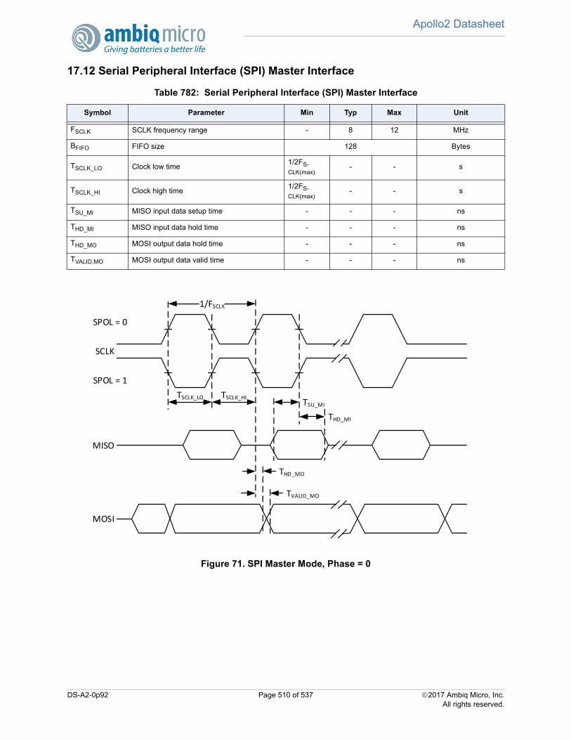
Apollo2 Datasheet
17.12 Serial Peripheral Interface (SPI) Master Interface
Figure 71. SPI Master Mode, Phase = 0
Table 782: Serial Peripheral Interface (SPI) Master Interface
Symbol Parameter Min Typ Max Unit
FSCLK SCLK frequency range - 8 12 MHz
BFIFO FIFO size 128 Bytes
TSCLK_LO Clock low time1/2FS-CLK(max)
- - s
TSCLK_HI Clock high time1/2FS-CLK(max)
- - s
TSU_MI MISO input data setup time - - - ns
THD_MI MISO input data hold time - - - ns
THD_MO MOSI output data hold time - - - ns
TVALID,MO MOSI output data valid time - - - ns
SCLK
MISO
TSU_MI
TSCLK_HITSCLK_LO
1/FSCLK
TVALID_MO
THD_MO
MOSI
THD_MI
SPOL = 0
SPOL = 1
DS-A2-0p92 Page 510 of 537 2017 Ambiq Micro, Inc.All rights reserved.
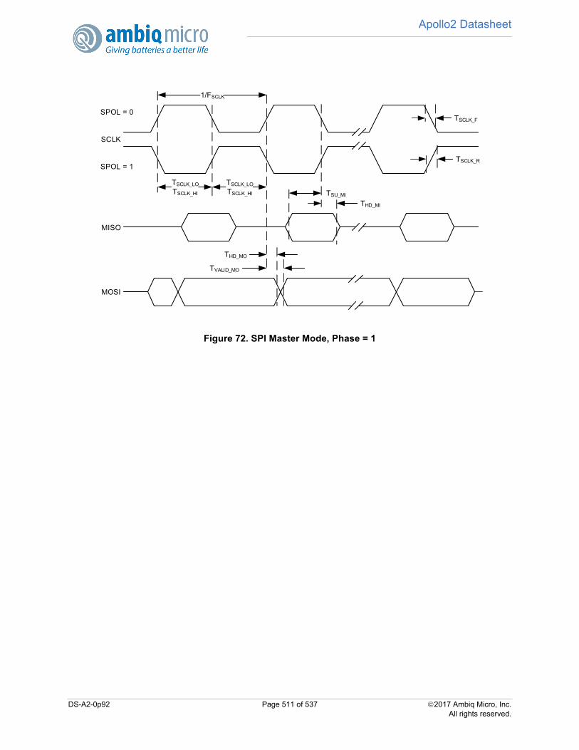
Apollo2 Datasheet
Figure 72. SPI Master Mode, Phase = 1
SCLK
MISO
THD_MI
TSCLK_LO
TSCLK_HI
TSCLK_LO
TSCLK_HI
1/FSCLK
THD_MO
TVALID_MO
SPOL = 0
SPOL = 1
MOSI
TSU_MI
TSCLK_R
TSCLK_F
DS-A2-0p92 Page 511 of 537 2017 Ambiq Micro, Inc.All rights reserved.

Apollo2 Datasheet
17.13 High Speed Serial Peripheral Interface (SPI) Master Interface
Figure 73. SPI Master Mode, Phase = 0
Table 783: High Speed Serial Peripheral Interface (SPI) Master Interface
Symbol Parameter Min Typ Max Unit
FSCLK SCLK frequency range - 12 24 MHz
BFIFO FIFO size 128 Bytes
TSCLK_LO Clock low time1/2FS-CLK(max)
- - s
TSCLK_HI Clock high time1/2FS-CLK(max)
- - s
TSU_MI MISO input data setup time - - - ns
THD_MI MISO input data hold time - - - ns
THD_MO MOSI output data hold time - - - ns
TVALID,MO MOSI output data valid time - - - ns
SCLK
MISO
TSU_MI
TSCLK_HITSCLK_LO
1/FSCLK
TVALID_MO
THD_MO
MOSI
THD_MI
SPOL = 0
SPOL = 1
DS-A2-0p92 Page 512 of 537 2017 Ambiq Micro, Inc.All rights reserved.

Apollo2 Datasheet
Figure 74. SPI Master Mode, Phase = 1
SCLK
MISO
THD_MI
TSCLK_LO
TSCLK_HI
TSCLK_LO
TSCLK_HI
1/FSCLK
THD_MO
TVALID_MO
SPOL = 0
SPOL = 1
MOSI
TSU_MI
TSCLK_R
TSCLK_F
DS-A2-0p92 Page 513 of 537 2017 Ambiq Micro, Inc.All rights reserved.
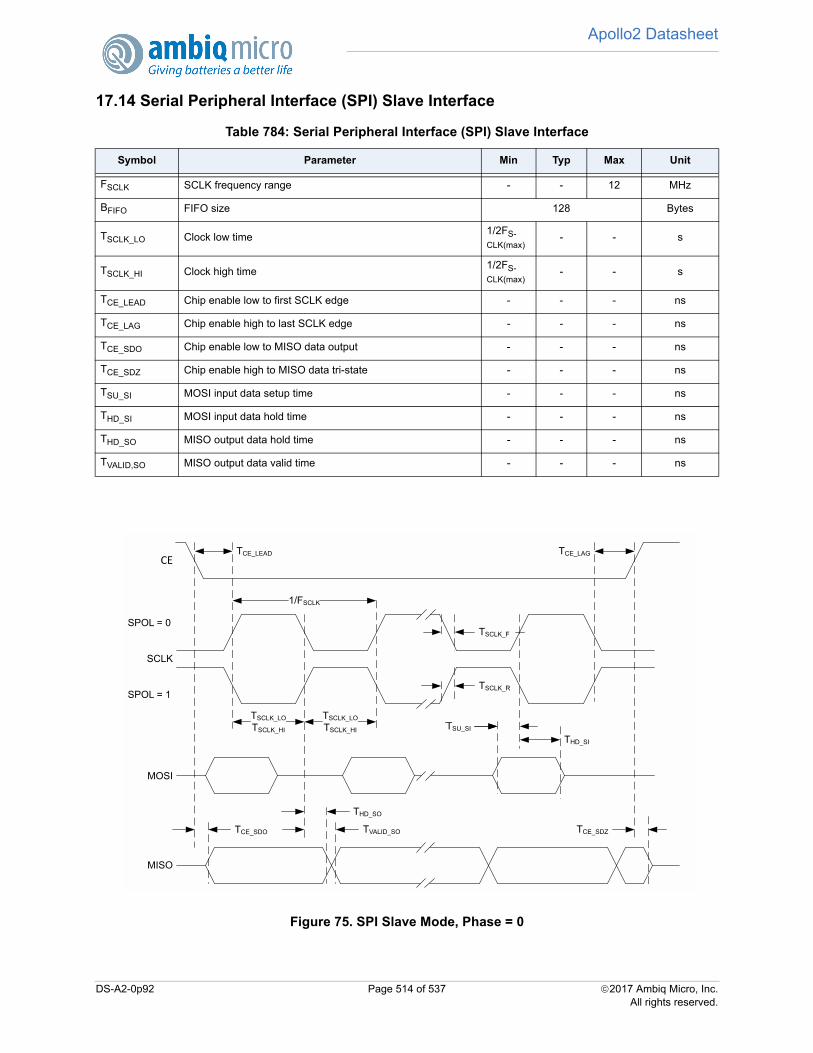
Apollo2 Datasheet
17.14 Serial Peripheral Interface (SPI) Slave Interface
Figure 75. SPI Slave Mode, Phase = 0
Table 784: Serial Peripheral Interface (SPI) Slave Interface
Symbol Parameter Min Typ Max Unit
FSCLK SCLK frequency range - - 12 MHz
BFIFO FIFO size 128 Bytes
TSCLK_LO Clock low time1/2FS-CLK(max)
- - s
TSCLK_HI Clock high time1/2FS-CLK(max)
- - s
TCE_LEAD Chip enable low to first SCLK edge - - - ns
TCE_LAG Chip enable high to last SCLK edge - - - ns
TCE_SDO Chip enable low to MISO data output - - - ns
TCE_SDZ Chip enable high to MISO data tri-state - - - ns
TSU_SI MOSI input data setup time - - - ns
THD_SI MOSI input data hold time - - - ns
THD_SO MISO output data hold time - - - ns
TVALID,SO MISO output data valid time - - - ns
SCLK
MOSI
THD_SI
TSCLK_LOTSCLK_HI
TSCLK_LOTSCLK_HI
1/FSCLK
THD_SO
TVALID_SO
TSU_MI
SPOL = 0
SPOL = 1
MISO
TSU_SI
TSCLK_R
TSCLK_F
CE
TCE_SDO
TCE_LEAD TCE_LAG
TCE_SDZ
DS-A2-0p92 Page 514 of 537 2017 Ambiq Micro, Inc.All rights reserved.

Apollo2 Datasheet
Figure 76. SPI Slave Mode, Phase = 1
SCLK
MOSI
THD_SI
TSCLK_LOTSCLK_HI
TSCLK_LOTSCLK_HI
1/FSCLK
THD_SO
TVALID_SO
SPOL = 0
SPOL = 1
MISO
TSU_SI
TSCLK_R
TSCLK_F
CETCE_LEAD TCE_LAG
TCE_SDO TCE_SDZ
DS-A2-0p92 Page 515 of 537 2017 Ambiq Micro, Inc.All rights reserved.
Apollo2 Datasheet
17.15 PDM Interface
17.16I2S Interface
17.17 Universal Asynchronous Receiver/Transmitter (UART)
17.18 Counter/Timer (CTIMER)
Table 785: Pulse Density Modulation (PDM) Interface
Symbol Parameter Min Typ Max Unit
DCPDMCLK PDM clock duty cycle1
1. Applicable to PDM_PCFG_MCLKDIV setting of MCKDIV1, MCKDIV2 or MCKDIV4 only. PDM_PCFG_MCLKDIV setting ofMCKDIV3 has a duty cycle of 67%.
45 - 55 %
TPDM_RISE PDM clock and data rise time - - TBD ns
TPDM_FALL PDM clock and data fall time - - TBD ns
TSU_PDM PDM input data setup time - - TBD ns
THD_PDM PDM input data hold time TBD - - ns
Table 786: Inter-Integrated Serial (I2S) Interface
Symbol Parameter Min Typ Max Unit
FBCLK I2S input BCLK frequency range TBD TBD MHz
FWDCLK I2S input WDCLK frequency range TBD TBD MHz
DCBCLK I2S BCLK duty cycle 40 - 60 %
DCWDCLK I2S WDCLK duty cycle 40 - 69 %
TI2S_RISE I2S clock and data rise time - - TBD ns
TI2S_FALL I2S clock and data fall time - - TBD ns
TSU_I2S I2S input data setup time - - TBD ns
THD_I2S I2S input data hold time TBD - - ns
Table 787: Universal Asynchronous Receiver/Transmitter (UART)
Symbol Parameter Min Typ Max Unit
FBAUD UART baud rate - 921600 bps
Table 788: Counter/Timer (CTIMER)
Symbol Parameter Min Typ Max Unit
FCTIMER Input frequency - - 24 MHz
TCTIMER Capture pulse width - - - µs
DS-A2-0p92 Page 516 of 537 2017 Ambiq Micro, Inc.All rights reserved.
Apollo2 Datasheet
17.19 Flash Memory
17.20 General Purpose Input/Output (GPIO)All GPIOs have Schmitt trigger inputs.
Table 789: Flash Memory
Symbol Parameter Min Typ Max Unit
PECYC Program/erase cycles before failure 10,000 - - cycles
TFDR Data retention @85C 10 - - years
TPAGE_ERASE Single page erase time (8192 bytes) 10 (TBD) - 20 (TBD) ms
TMASS_ERASE Mass erase time 10 (TBD) - 20 (TBD) ms
Table 790: General Purpose Input/Output (GPIO)
Symbol Parameter Min TYP Max Unit
ALL GPIOs
VOH High-level output voltage 0.8 * VDDH - - V
VOL Low-level output voltage - - 0.2 * VDDH V
VIH Positive going input threshold voltage 0.7 * VDDH - V
VIL Negative going input threshold voltage - 0.3 * VDDH V
VHYS Input Hysteresis 0.1 * VDDH - V
CGPI Input capacitance - TBD pF
RPU Pull-up resistance - 63 - kΩ
RPD Pull-down resistance - 63 - kΩ
RPUI2C00 I2C pad pull-up resistance, RSEL = 0x00 - 2 - kΩ
RPUI2C01 I2C pad pull-up resistance, RSEL = 0x01 - 6 - kΩ
RPUI2C10 I2C pad pull-up resistance, RSEL = 0x10 - 12 - kΩ
RPUI2C11 I2C pad pull-up resistance, RSEL = 0x11 - 24 - kΩ
IIN Input pin leakage current - 1 - nA
IINOD Open drain output leakage current - 1 - nA
STANDARD GPIOs
TRISE_STD Rise time - - TBD ns
TFALL_STD Fall time - - TBD ns
ISRC_STD Output source current, 2mA drive strength - 3.5 - mA
ISNK_STD Output sink current, 2mA drive strength - 3.4 - mA
ISRC_STD Output source current, 4mA drive strength - 7.1 - mA
ISNK_STD Output sink current, 4mA drive strength - 6.8 - mA
ISRC_STD Output source current, 8mA drive strength - 14.1 - mA
ISNK_STD Output sink current, 8mA drive strength - 13.5 - mA
DS-A2-0p92 Page 517 of 537 2017 Ambiq Micro, Inc.All rights reserved.
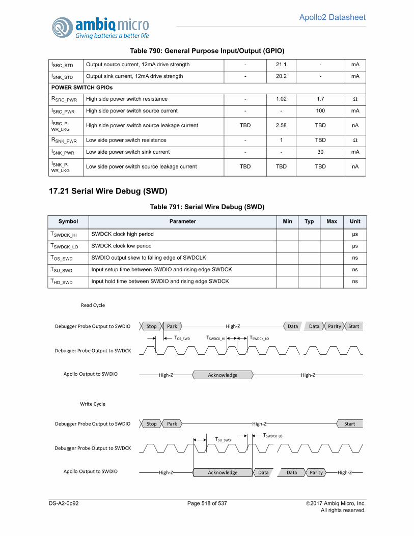
Apollo2 Datasheet
17.21 Serial Wire Debug (SWD)
ISRC_STD Output source current, 12mA drive strength - 21.1 - mA
ISNK_STD Output sink current, 12mA drive strength - 20.2 - mA
POWER SWITCH GPIOs
RSRC_PWR High side power switch resistance - 1.02 1.7 Ω
ISRC_PWR High side power switch source current - - 100 mA
ISRC_P-WR_LKG
High side power switch source leakage current TBD 2.58 TBD nA
RSNK_PWR Low side power switch resistance - 1 TBD Ω
ISNK_PWR Low side power switch sink current - - 30 mA
ISNK_P-WR_LKG
Low side power switch source leakage current TBD TBD TBD nA
Table 791: Serial Wire Debug (SWD)
Symbol Parameter Min Typ Max Unit
TSWDCK_HI SWDCK clock high period µs
TSWDCK_LO SWDCK clock low period µs
TOS_SWD SWDIO output skew to falling edge of SWDCLK ns
TSU_SWD Input setup time between SWDIO and rising edge SWDCK ns
THD_SWD Input hold time between SWDIO and rising edge SWDCK ns
Table 790: General Purpose Input/Output (GPIO)
StartParityDataDataParkStopDebugger Probe Output to SWDIO High‐Z
Debugger Probe Output to SWDCK
AcknowledgeHigh‐Z High‐Z
TOS_SWD TSWDCK_HI TSWDCK_LO
Read Cycle
Apollo Output to SWDIO
Start
ParityDataData
ParkStopDebugger Probe Output to SWDIO High‐Z
Debugger Probe Output to SWDCK
AcknowledgeHigh‐Z High‐Z
TSU_SWD
TSWDCK_LO
Write Cycle
Apollo Output to SWDIO
DS-A2-0p92 Page 518 of 537 2017 Ambiq Micro, Inc.All rights reserved.

Apollo2 Datasheet
Figure 77. Serial Wire Debug Timing
DS-A2-0p92 Page 519 of 537 2017 Ambiq Micro, Inc.All rights reserved.
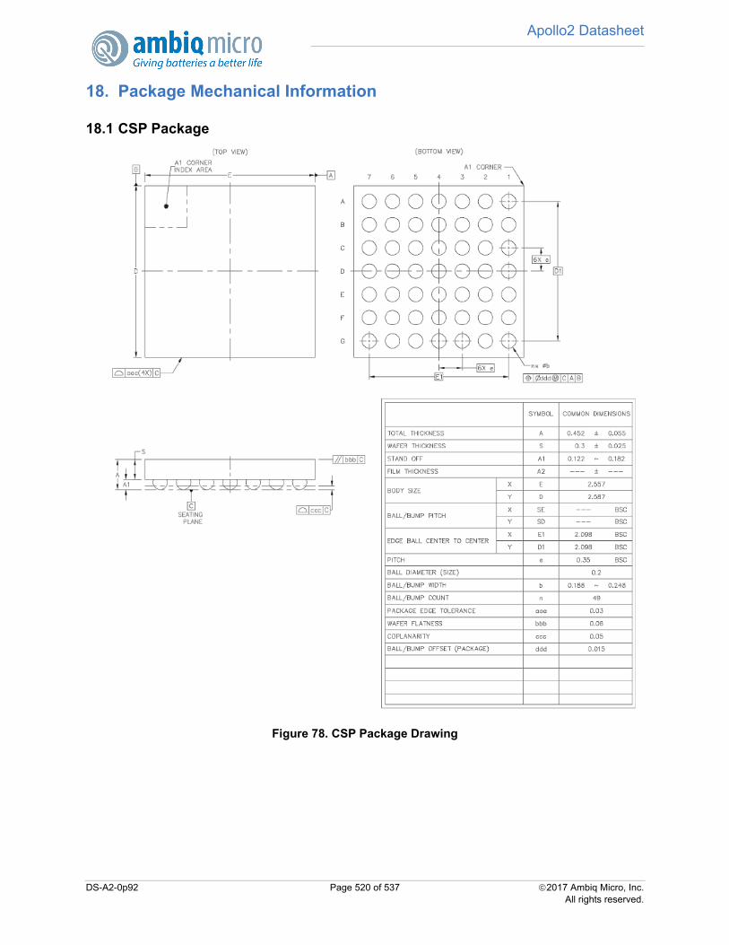
Apollo2 Datasheet
18. Package Mechanical Information
18.1 CSP Package
Figure 78. CSP Package Drawing
DS-A2-0p92 Page 520 of 537 2017 Ambiq Micro, Inc.All rights reserved.
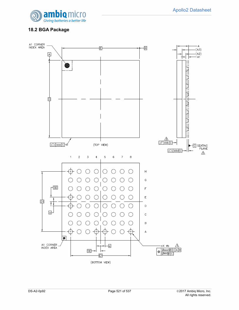
Apollo2 Datasheet
18.2 BGA Package
DS-A2-0p92 Page 521 of 537 2017 Ambiq Micro, Inc.All rights reserved.

Apollo2 Datasheet
Drawing Notes:Dimension B is measured at the maximum solder ball diameter , parallel to datum plane cDatum C (seating plane) is defined by the spherical crowns of solder balls.Parallelism measurement shall exclude effect of mark on top surface of package.
Figure 79. BGA Package Drawing
18.2.1 PCB land pattern and solder stencil
For the BGA package, there should be a 1:1 ratio between the diameter of the PCB pad and the diameterof the BGA ball. If required by routing constraints, the ratio of the PCB pad to the BGA ball may be 0.8:1.The solder stencil should leave a solder mask opening that allows for 0.0762 mm clearance around thePCB pad (diameter 0.1524 mm larger than the PCB pad).
DS-A2-0p92 Page 522 of 537 2017 Ambiq Micro, Inc.All rights reserved.
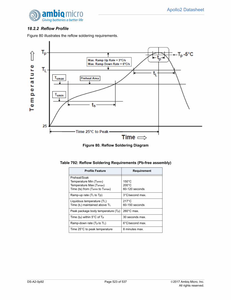
Apollo2 Datasheet
18.2.2 Reflow Profile
Figure 80 illustrates the reflow soldering requirements.
Figure 80. Reflow Soldering Diagram
Table 792: Reflow Soldering Requirements (Pb-free assembly)
Profile Feature Requirement
Preheat/SoakTemperature Min (Tsmin)Temperature Max (Tsmax)Time (ts) from (Tsmin to Tsmax)
150°C200°C60-120 seconds
Ramp-up rate (TL to Tp) 3°C/second max.
Liquidous temperature (TL)Time (tL) maintained above TL
217°C60-150 seconds
Peak package body temperature (Tp) 260°C max.
Time (tp) within 5°C of Tp 30 seconds max.
Ramp-down rate (Tp to TL) 6°C/second max.
Time 25°C to peak temperature 8 minutes max.
DS-A2-0p92 Page 523 of 537 2017 Ambiq Micro, Inc.All rights reserved.

Apollo2 Datasheet
DS-A2-0p92 Page 524 of 537 2017 Ambiq Micro, Inc.All rights reserved.
Apollo2 Datasheet
Index
Numerics10BIT 14112/24 Hour Mode 3633-wire mode 144AAccess permissions 59accumulation control 457accumulation, automatic 457ACK 140, 176Acknowledge 140Active Mode 60ADC 53, 200, 244, 454ADC Configuration Register 462ADC Reference Generator 456ADC_DIV3 455ADC_EXT0 455ADC_EXT1 455ADC_EXT2 455ADC_EXT3 455ADC_EXT4 455ADC_EXT5 455ADC_EXT6 455ADC_EXT7 455ADCREF 244ADC_SWT 456ADC_TEMP 455ADC_TRIG0 456ADC_TRIG1 456ADC_TRIG2 456ADC_TRIG3 456ADC_VSS 455AHB 59, 168Alarm Registers 363ALM interrupt 363ALM100 363AM08XX, see real-time clockAM18XX, see real-time clockAMBA 59Analog Multiplexer Channel Selection 457analog mux 455analog-to-digital converter 53APB 59Architecture Reference Manual 60Area, Direct 169
DS-A2-0p92 Page 525 of 537 2017 Ambiq Micro, Inc.All rights reserved.
Apollo2 Datasheet
ARM, see processorARMv7 60Attachment, debugger 71Autoadjustment, HFRC 347Automatic Sample Accumulation 457BBandgap 456battery life 52BCD format 362Buck Converter Charge Insertion 376Buck Converters 498Bus Not Busy 140, 175bus, AMBA AHB 59bus, AMBA APB 59bus, DCode 59bus, ICode 59bus, System 59CCalibration, Distributed Digital 345, 346CALRC 345CALXT 346CLKOUT 344, 345, 347Clock Generator Module 344clock sources 53clock, interface 136CMPOUT 491CMPR0 374, 375CMPR1 375CONT 143Continuous 375control, accumulation 457converters, buck 498core, see processorCortex, see processorcounter, 32-bit 376CPHA 144, 147, 180CPOL 144, 147, 180CTRERR 362CTS 239, 241DData Valid 140, 176DCode 59debug 71Debug Interfaces 71debugger attachment 71Deep Sleep 344
DS-A2-0p92 Page 526 of 537 2017 Ambiq Micro, Inc.All rights reserved.
Apollo2 Datasheet
Deep Sleep Mode 59, 60Deep Slope Mode 180Direct Area 169Distributed Digital Calibration 345, 346EEG_IOSLAVE_FIFOPTR_FIFOSIZ 172event 54event, wakeup 60FFast Mode Plus 175fault handler, Memanage 59Faulting Address Trapping Hardware 72FIFO 169
Area Functions 172FIFOCTR 172FIFOPTR 172FIFOREM 139FIFORTHR 139FIFOSIZ 139, 172FIFOUPD 173FIFOWTHR 139flash 53GGPIO 221GPIO and Pad Configuration Module 217GPIOA_IER 222GPIOA_ISR 222GPIOA_WCR 222GPIOB_IER 222GPIOB_ISR 222GPIOB_WCR 222GPIOB_WSR 222GPIOEN 221GPIOENA 222GPIOENB 222GPIOnINCFG 222, 224GPIOn_INT 224GPIOnINTD 224GPIOnINTP 222GPIOnOUTCFG 223GPIORD 224GPIORDA 222GPIORDB 222GPIOWT 221, 222GPIOWTA 222GPIOWTB 222
DS-A2-0p92 Page 527 of 537 2017 Ambiq Micro, Inc.All rights reserved.
Apollo2 Datasheet
GPIOWTCA 222GPIOWTCB 222GPIOWTSA 222GPIOWTSB 222HHardware, Fault Address Trapping 72HFADJCK 347HFRC 347, 455HFRC Autoadjustment 347HFXTADJ 347High Frequency RC Oscillator 347HR1224 363II2C
10-bit addressing 1767-bit addressing 176ADDRESS 141Address 176Command 141FIFO 139I2CADDR 175, 176IO Master 0 224IO Master 0 Loopback 234IO Master 1 225, 226IO Master 1 Loopback 235IO Slave 233master 136Multi-master Arbitration 143Normal Read 142Normal Write 142Offset Address 141, 177Raw Read 143Raw Write 143Read 177receiver 139SCL 139SDA 139Slave 168, 175transmitter 139Write 177
I2C/SPI Master 344I2C/SPI Master Module 136ICode 59IE bit 373Instrumentation Trace Macrocell 71Instrumentation Trace Module 53
DS-A2-0p92 Page 528 of 537 2017 Ambiq Micro, Inc.All rights reserved.
Apollo2 Datasheet
interfaces, debug 71interrupt 54
ALM 363IOINT 173RDERR 173
InterruptsVector Table 54
IO Slave Interrupt 234IOINT 173IOREAD 173ITM, see Instrumentation Trace MacrocellLLDO 498LFRC 345, 348life, battery 52Loopback 234Low-Power Consumption Modes 54MManaged Conversion Slots 457map, memory 56Master Module , I2C/SPI 136MemManage 59memory 53
LRAM 139, 168RAM 53SRAM 59
memory map 56peripheral device 58
Memory Protection Unit 59MISO 144mode
Active 60Deep Sleep 60, 344Sleep 60
mode, Deep Sleep 59Module, ADC and Temperature Sensor 454module, PINCFG 144MOSI 144MPU, see Memory Protection Unitmux, analog 455NNAK 176Nested Vectored Interrupt Controller 54NSEL 491NVIC, see Nested Vectored Interrupt Controller
DS-A2-0p92 Page 529 of 537 2017 Ambiq Micro, Inc.All rights reserved.
Apollo2 Datasheet
OOPER 141oscillator
High Frequency RC 347high frequency RC 53, 344, 455low frequency RC 53, 344, 345RC 53XTAL 53, 344, 345XTAL Failure Detection 348
OUTDATSEL 222OUTENSEL 222, 223, 224PPAD10PULL 227, 228, 229, 230, 231PAD20FNCSEL 246PAD20INPEN 246PAD21INPEN 246PAD5INPEN 224, 226PAD5PULL 224, 226PAD5RSEL 224PAD6INPEN 224, 226PAD6PULL 224, 226PAD6RSEL 224PAD7PULL 226PAD8INPEN 225, 226, 227, 228, 229, 230, 231PAD8PULL 225, 226, 227, 228, 229, 230, 231PAD9INPEN 225, 226, 227, 228, 229, 230, 231PAD9PULL 225, 226, 227, 228, 229, 230, 231PADKEY 221PADnFNCSEL 217–??, 221PADnINPEN 224, 228, 229, 230, 231, 238, 240, 242, 243PADnPULL 218, 224, 228, 229, 230, 231, 238, 240, 242, 243PADnRSEL 224PADnSTRNG 223Peripheral Device Memory Map 58PINCFG 144power 52power modes 60Power Optimization 376power-on reset 60processor 53Protected Memory System Architecture 59Protection regions 59PSEL 491PTAT 491PWDKEY 491
DS-A2-0p92 Page 530 of 537 2017 Ambiq Micro, Inc.All rights reserved.
Apollo2 Datasheet
RRDERR 173Real Time Clock Module 348real-time clock 53REG_CLK_GEN_ALMLOW_ALM100 363REG_CLK_GEN_ALMLOW_ALMHR 363REG_CLK_GEN_ALMLOW_ALMMIN 363REG_CLK_GEN_ALMLOW_ALMSEC 363REG_CLK_GEN_ALMUP_ALMDATE 363REG_CLK_GEN_ALMUP_ALMMO 363REG_CLK_GEN_ALMUP_ALMWKDY 363REG_CLKGEN_CALXT 346REG_CLK_GEN_CTRLOW_CTR100 362REG_CLK_GEN_CTRLOW_CTRHR 362REG_CLK_GEN_CTRLOW_CTRMIN 362REG_CLK_GEN_CTRLOW_CTRSEC 362REG_CLK_GEN_CTRUP_CB 362REG_CLK_GEN_CTRUP_CEB 363REG_CLK_GEN_CTRUP_CTRDATE 362REG_CLK_GEN_CTRUP_CTRERR 362REG_CLK_GEN_CTRUP_CTRMO 362REG_CLK_GEN_CTRUP_CTRWKDY 362REG_CLK_GEN_CTRUP_CTRYR 362REG_CLKGEN_HFADJ_HFADJEN 347REG_CLKGEN_HFTUNERB 347REG_CLKGEN_OCTRL_OSEL 345, 346REG_CLK_GEN_RTCCTL_HR1224 363REG_CLK_GEN_RTCCTL_RPT 363REG_CLK_GEN_RTCCTL_RSTOP 362REG_CLK_GEN_RTCCTL_WRTC 362REG_CLKGEN_STATUS_OMODE 346REG_CLKGEN_STATUS_OSCF 346REG_CTIMER_CMPR0 373REG_CTIMER_CMPR0/1 372REG_CTIMER_CTCTRLx_CTRLINKx 376REG_CTIMER_CTCTRLx_TMRxyFN 372REG_CTIMER_TMRxyCLR 373REG_CTIMER_TMRxyEN 374REG_CTIMER_TMRxyIE 374REG_CTIMER_TMRxyPE 373, 374REG_CTIMER_TMRxyPOL 374REG_GPIO_GPIOCFGy 221REG_GPIO_GPIOyCFG_GPIOnOUTCFG 221REG_GPIO_PADKEY 217REG_GPIO_PADREG 217REG_GPIO_PADREGy_PAD11PWRDN 218
DS-A2-0p92 Page 531 of 537 2017 Ambiq Micro, Inc.All rights reserved.
Apollo2 Datasheet
REG_GPIO_PADREGy_PAD20PULL 218REG_GPIO_PADREGy_PAD3PWRUP 218REG_GPIO_PADREGy_PAD4PWRUP 218REG_GPIO_PADREGy_PADnFNCSEL 217REG_GPIO_PADREGy_PADnINPEN 218REG_GPIO_PADREGy_PADnPULL 218REG_GPIO_PADREGy_PADnSTRNG 217REG_IOMSTRn_CLKCFG_DIV3 136REG_IOMSTRn_CLKCFG_DIVEN 137REG_IOMSTRn_CLKCFG_FSEL 136REG_IOMSTRn_CLKCFG_LOWPER 137REG_IOMSTRn_CLKCFG_TOTPER 137REG_IOMSTRn_CMD 138REG_IOMSTRn_FIFOPTR_FIFOREM 139REG_IOMSTRn_FIFOPTR_FIFOSIZ 139REG_IOMSTRn_FIFOTHR_FIFOWTHR 138REG_IOMSTRn_IOMCFG_SPHA 144REG_IOMSTRn_IOMCFG_SPOL 144REG_IOSLAVE_FIFOCFG_FIFOBASE 169REG_IOSLAVE_FIFOCFG_FIFOMAX 169REG_IOSLAVE_FIFOCFG_ROBASE 172REG_IOSLAVE_FIFOCTR 172REG_IOSLAVE_FIFOPTR_FIFOPTR 172REG_IOSLAVE_FUPD_FIFOUPD 173REG_IOSLAVE_FUPD_IOREAD 173REG_IOSLAVE_IOSCFG_I2CADDR 175REG_IOSLAVE_IOSCFG_LSB 180REG_IOSLAVE_PRENC 172Repeated Count 373Repeated Pulse 374Reset Module 430reset, power-on 60RESTART 175RSTn 430RTC, see real-time clockRTS 239, 241SSAR, see Successive Approximation RegisterSCR, see System Control RegisterSerial Wire Debug 71Serial Wire Debugger 53Single Count 373Single Pulse 374Sleep Mode 60, 180SLEEPONEXIT 60Slots, Mananged Conversion 457
DS-A2-0p92 Page 532 of 537 2017 Ambiq Micro, Inc.All rights reserved.

Apollo2 Datasheet
SPHA 147SPI 144
3-wire 179CHANNEL 144CMD Register 144Complex Operations 146frequency 137IO Master 0 3-wire 231IO Master 0 4-wire 226IO Master 0 4-wire Loopback 235IO Master 1 3-wire 232, 233IO Master 1 4-wire 227, 228, 229, 230, 231IO Master 1 4-wire Loopback 235IO Slave 3-wire 234IO Slave 4-wire 234master 136Normal Read 145Normal Write 144OPER 144Phase 147Polarity 147Raw Read 146Raw Write 145Read 179Slave 168, 178slave 178Slave Addressing 144Write 178
SPOL 147, 180START 175Start Data Transfer 140, 175STOP 143, 175STOP condition 140Stop Data Transfer 140, 175Successive Approximation Register 53, 454SWD, see Serial Wire DebugSWD, see Serial Wire DebuggerSWDCK 246SWDIO 246SYSRESETREQn 430System Control Register 60TTemperature Sensor 454TMRWCR 373, 374TPIU, see Trace Port Interface UnitTrace Port Interface Unit 53, 72
DS-A2-0p92 Page 533 of 537 2017 Ambiq Micro, Inc.All rights reserved.
Apollo2 Datasheet
Track and Hold Time 457TRIGSEL 456TX 238, 240, 242, 243UUART 238, 347
CTS 239, 241RTS 239, 241RX 238, 240, 242, 243
UPLNGTH 144VVCOMP, see Voltage ComparatorVEXT1 491VEXT2 491Voltage Comparator 246, 491Voltage Regulator Module 498VREFEXT1 491VREFEXT2 491VREFEXT3 491VREFINT 491VTEMP 491WWait-For-Interrupt 60Wakeup 180wake-up 53Wake-Up Interrupt Controller 59Watchdog Timer 423WC bit 373WDTCFG 423WFI, see Wait-For-InterruptWIC, see wake-upWindow Comparisons 457XXT 345, 348XT Oscillator 345
DS-A2-0p92 Page 534 of 537 2017 Ambiq Micro, Inc.All rights reserved.
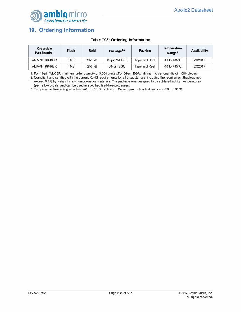
Apollo2 Datasheet
537
19. Ordering Information
Table 793: Ordering Information
Orderable Part Number
Flash RAM Package1,2
1. For 49-pin WLCSP, minimum order quantity of 5,000 pieces.For 64-pin BGA, minimum order quantity of 4,000 pieces.2. Compliant and certified with the current RoHS requirements for all 6 substances, including the requirement that lead not
exceed 0.1% by weight in raw homogeneous materials. The package was designed to be soldered at high temperatures (per reflow profile) and can be used in specified lead-free processes.
PackingTemperature
Range3
3. Temperature Range is guaranteed -40 to +85°C by design. Current production test limits are -20 to +60°C.
Availability
AMAPH1KK-KCR 1 MB 256 kB 49-pin WLCSP Tape and Reel -40 to +85°C 2Q2017
AMAPH1KK-KBR 1 MB 256 kB 64-pin BGQ Tape and Reel -40 to +85°C 2Q2017
DS-A2-0p92 Page 535 of 537 2017 Ambiq Micro, Inc.All rights reserved.
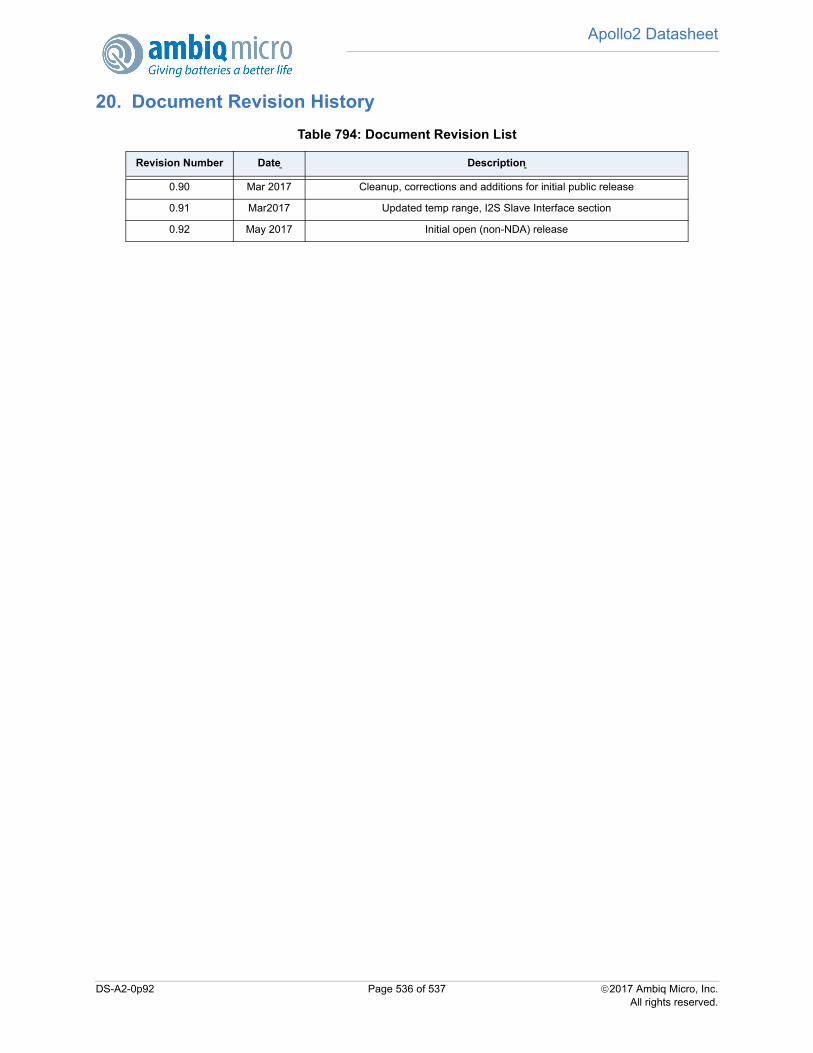
Apollo2 Datasheet
537
20. Document Revision History
Table 794: Document Revision List
Revision Number Date Description
0.90 Mar 2017 Cleanup, corrections and additions for initial public release
0.91 Mar2017 Updated temp range, I2S Slave Interface section
0.92 May 2017 Initial open (non-NDA) release
DS-A2-0p92 Page 536 of 537 2017 Ambiq Micro, Inc.All rights reserved.
Apollo2 Datasheet
537
Contact Information
Address Ambiq Micro, Inc.
6500 River Place Blvd.
Building 7, Suite 200
Austin, TX 78730-1156
Phone +1 (512) 879-2850
Website http://www.ambiqmicro.com/
General Information [email protected]
Sales [email protected]
Technical Support [email protected]
Legal Information and DisclaimersAMBIQ MICRO INTENDS FOR THE CONTENT CONTAINED IN THE DOCUMENT TO BE ACCURATE AND RELIABLE. THIS CONTENT MAY, HOW-EVER, CONTAIN TECHNICAL INACCURACIES, TYPOGRAPHICAL ERRORS OR OTHER MISTAKES. AMBIQ MICRO MAY MAKE CORRECTIONSOR OTHER CHANGES TO THIS CONTENT AT ANY TIME. AMBIQ MICRO AND ITS SUPPLIERS RESERVE THE RIGHT TO MAKE CORRECTIONS,MODIFICATIONS, ENHANCEMENTS, IMPROVEMENTS AND OTHER CHANGES TO ITS PRODUCTS, PROGRAMS AND SERVICES AT ANY TIMEOR TO DISCONTINUE ANY PRODUCTS, PROGRAMS, OR SERVICES WITHOUT NOTICE.
THE CONTENT IN THIS DOCUMENT IS PROVIDED "AS IS". AMBIQ MICRO AND ITS RESPECTIVE SUPPLIERS MAKE NO REPRESENTATIONSABOUT THE SUITABILITY OF THIS CONTENT FOR ANY PURPOSE AND DISCLAIM ALL WARRANTIES AND CONDITIONS WITH REGARD TOTHIS CONTENT, INCLUDING BUT NOT LIMITED TO, ALL IMPLIED WARRANTIES AND CONDITIONS OF MERCHANTABILITY, FITNESS FOR APARTICULAR PURPOSE, TITLE AND NON-INFRINGEMENT OF ANY THIRD PARTY INTELLECTUAL PROPERTY RIGHT.
AMBIQ MICRO DOES NOT WARRANT OR REPRESENT THAT ANY LICENSE, EITHER EXPRESS OR IMPLIED, IS GRANTED UNDER ANY PAT-ENT RIGHT, COPYRIGHT, MASK WORK RIGHT, OR OTHER INTELLECTUAL PROPERTY RIGHT OF AMBIQ MICRO COVERING OR RELATING TOTHIS CONTENT OR ANY COMBINATION, MACHINE, OR PROCESS TO WHICH THIS CONTENT RELATE OR WITH WHICH THIS CONTENT MAYBE USED.
USE OF THE INFORMATION IN THIS DOCUMENT MAY REQUIRE A LICENSE FROM A THIRD PARTY UNDER THE PATENTS OR OTHER INTEL-LECTUAL PROPERTY OF THAT THIRD PARTY, OR A LICENSE FROM AMBIQ MICRO UNDER THE PATENTS OR OTHER INTELLECTUAL PROP-ERTY OF AMBIQ MICRO.
INFORMATION IN THIS DOCUMENT IS PROVIDED SOLELY TO ENABLE SYSTEM AND SOFTWARE IMPLEMENTERS TO USE AMBIQ MICROPRODUCTS. THERE ARE NO EXPRESS OR IMPLIED COPYRIGHT LICENSES GRANTED HEREUNDER TO DESIGN OR FABRICATE ANY INTE-GRATED CIRCUITS OR INTEGRATED CIRCUITS BASED ON THE INFORMATION IN THIS DOCUMENT. AMBIQ MICRO RESERVES THE RIGHTTO MAKE CHANGES WITHOUT FURTHER NOTICE TO ANY PRODUCTS HEREIN. AMBIQ MICRO MAKES NO WARRANTY, REPRESENTATIONOR GUARANTEE REGARDING THE SUITABILITY OF ITS PRODUCTS FOR ANY PARTICULAR PURPOSE, NOR DOES AMBIQ MICRO ASSUMEANY LIABILITY ARISING OUT OF THE APPLICATION OR USE OF ANY PRODUCT OR CIRCUIT, AND SPECIFICALLY DISCLAIMS ANY AND ALLLIABILITY, INCLUDING WITHOUT LIMITATION CONSEQUENTIAL OR INCIDENTAL DAMAGES. “TYPICAL” PARAMETERS WHICH MAY BE PRO-VIDED IN AMBIQ MICRO DATA SHEETS AND/OR SPECIFICATIONS CAN AND DO VARY IN DIFFERENT APPLICATIONS AND ACTUAL PERFOR-MANCE MAY VARY OVER TIME. ALL OPERATING PARAMETERS, INCLUDING “TYPICALS” MUST BE VALIDATED FOR EACH CUSTOMERAPPLICATION BY CUSTOMER’S TECHNICAL EXPERTS. AMBIQ MICRO DOES NOT CONVEY ANY LICENSE UNDER NEITHER ITS PATENTRIGHTS NOR THE RIGHTS OF OTHERS. AMBIQ MICRO PRODUCTS ARE NOT DESIGNED, INTENDED, OR AUTHORIZED FOR USE AS COMPO-NENTS IN SYSTEMS INTENDED FOR SURGICAL IMPLANT INTO THE BODY, OR OTHER APPLICATIONS INTENDED TO SUPPORT OR SUSTAINLIFE, OR FOR ANY OTHER APPLICATION IN WHICH THE FAILURE OF THE AMBIQ MICRO PRODUCT COULD CREATE A SITUATION WHEREPERSONAL INJURY OR DEATH MAY OCCUR. SHOULD BUYER PURCHASE OR USE AMBIQ MICRO PRODUCTS FOR ANY SUCH UNINTENDEDOR UNAUTHORIZED APPLICATION, BUYER SHALL INDEMNIFY AND HOLD AMBIQ MICRO AND ITS OFFICERS, EMPLOYEES, SUBSIDIARIES,AFFILIATES, AND DISTRIBUTORS HARMLESS AGAINST ALL CLAIMS, COSTS, DAMAGES, AND EXPENSES, AND REASONABLE ATTORNEYFEES ARISING OUT OF, DIRECTLY OR INDIRECTLY, ANY CLAIM OF PERSONAL INJURY OR DEATH ASSOCIATED WITH SUCH UNINTENDEDOR UNAUTHORIZED USE, EVEN IF SUCH CLAIM ALLEGES THAT AMBIQ MICRO WAS NEGLIGENT REGARDING THE DESIGN OR MANUFAC-TURE OF THE PART.
DS-A2-0p92 Page 537 of 537 2017 Ambiq Micro, Inc.All rights reserved.