ansys maxwell 3d v16oss.jishulink.com/caenet/forums/upload/2014/09/20/389/... · 21/5/2013 · ©...
TRANSCRIPT
© 2013 ANSYS, Inc. May 21, 2013 1 Release 14.5
Workshop 7: Basic Electric Transient Analysis
ANSYS Maxwell 3D V16
© 2013 ANSYS, Inc. May 21, 2013 2 Release 14.5
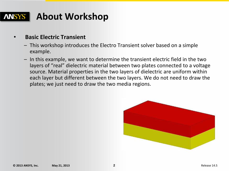
About Workshop
• Basic Electric Transient
– This workshop introduces the Electro Transient solver based on a simple example.
– In this example, we want to determine the transient electric field in the two layers of “real” dielectric material between two plates connected to a voltage source. Material properties in the two layers of dielectric are uniform within each layer but different between the two layers. We do not need to draw the plates; we just need to draw the two media regions.

© 2013 ANSYS, Inc. May 21, 2013 3 Release 14.5
Problem Setup
• Create Design
– Select the menu item Project Insert Maxwell 3D Design, or click on the icon
• Set the Solution Type:
– Select the menu item Maxwell 3D Solution Type
– Solution Type Window:
1. Choose Electric > Electric Transient
2. Click the OK button

© 2013 ANSYS, Inc. May 21, 2013 4 Release 14.5
Create Geometry
• Create Box_Bottom – Select the menu item Draw Box
1. Using the coordinate entry fields, enter the box position
– X: -1, Y: -2, Z: -0.6, Press the Enter key
2. Using the coordinate entry fields, enter the opposite corner
– dX: 2, dY: 4, dZ: 0.6, Press the Enter key
– Change the name of the Object to Box_Bottom
• Create Box_Top – Select the object Box_Bottom from the history tree
– Select the menu item Edit Duplicate Along Line
1. Using the coordinate entry fields, enter the first point of duplicate vector
– X: 0, Y: 0, Z: 0, Press the Enter key
2. Using the coordinate entry fields, enter the opposite corner
– dX: 0, dY: 0, dZ: 0.6, Press the Enter key
3. Total Number: 2
4. Press OK
– Change the name of the Object to Box_Top

© 2013 ANSYS, Inc. May 21, 2013 5 Release 14.5
Define Material
• Create Material for Box_Bottom – Select the object Box_Bottom, right click and select Assign Material
– In Select Definition window, select Add Material
1. In View/Edit Material window,
– Material Name: Mat_Bottom
– Relative Permittivity: 5
– Bulk Conductivity: 1e-7 siemens/m
– Select OK
• Create Material for Box_Top – Select the object Box_Top, right click and select Assign Material
– In Select Definition window, select Add Material
1. In View/Edit Material window,
– Material Name: Mat_Top
– Relative Permittivity: 4
– Bulk Conductivity: 2e-8 siemens/m
– Select OK
© 2013 ANSYS, Inc. May 21, 2013 6 Release 14.5
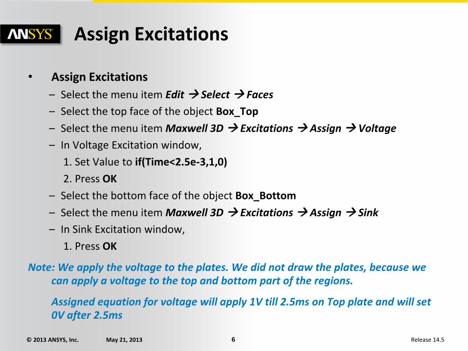
Assign Excitations
• Assign Excitations
– Select the menu item Edit Select Faces
– Select the top face of the object Box_Top
– Select the menu item Maxwell 3D Excitations Assign Voltage
– In Voltage Excitation window,
1. Set Value to if(Time<2.5e-3,1,0)
2. Press OK
– Select the bottom face of the object Box_Bottom
– Select the menu item Maxwell 3D Excitations Assign Sink
– In Sink Excitation window,
1. Press OK
Note: We apply the voltage to the plates. We did not draw the plates, because we can apply a voltage to the top and bottom part of the regions.
Assigned equation for voltage will apply 1V till 2.5ms on Top plate and will set 0V after 2.5ms

© 2013 ANSYS, Inc. May 21, 2013 7 Release 14.5
Assign Mesh operations
• Assign Mesh operations – Select the menu item Edit Select Objects
– Press Ctrl and select the objects Box_Bottom and Box_Top
– Select the menu item Maxwell 3D Mesh Operations Assign Inside Selection Length Based
– In Element Length Based Refinement window,
1. Restrict length of Elements: Checked
2. Maximum Length of Elements: 0.55 mm
3. Press OK
• Create Points for – Select the menu item Draw Point
1. Using the coordinate entry fields, enter the point position
– X: 0, Y: 0, Z: 0.3, Press the Enter key
– Select the menu item Draw Point
1. Using the coordinate entry fields, enter the point position
– X: 0, Y: 0, Z: -0.3, Press the Enter key

© 2013 ANSYS, Inc. May 21, 2013 8 Release 14.5
Analyze
• Create an analysis setup:
– Select the menu item Maxwell 3D Analysis Setup Add Solution Setup
– Solution Setup Window:
1. General Tab
– Stop Time: 5 ms
– Initial Time Step: 1us
– Maximum Time Step: 10 us
– Save Fields: Checked
2. Click the OK button
Note: Electric transient solver uses adaptive time stepping approach.
• Start the solution process:
1. Select the menu item Maxwell 3D Analyze All
© 2013 ANSYS, Inc. May 21, 2013 9 Release 14.5
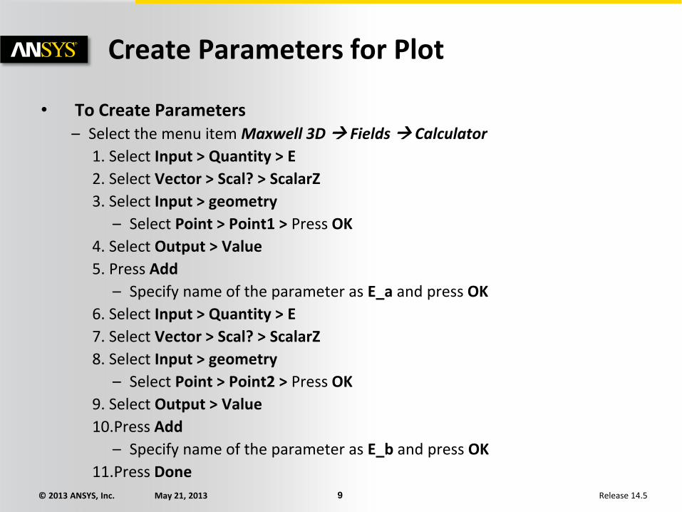
Create Parameters for Plot
• To Create Parameters – Select the menu item Maxwell 3D Fields Calculator
1. Select Input > Quantity > E
2. Select Vector > Scal? > ScalarZ
3. Select Input > geometry
– Select Point > Point1 > Press OK
4. Select Output > Value
5. Press Add
– Specify name of the parameter as E_a and press OK
6. Select Input > Quantity > E
7. Select Vector > Scal? > ScalarZ
8. Select Input > geometry
– Select Point > Point2 > Press OK
9. Select Output > Value
10.Press Add
– Specify name of the parameter as E_b and press OK
11.Press Done

© 2013 ANSYS, Inc. May 21, 2013 10 Release 14.5
Create Plot
• Create Plot
– Select the menu item Maxwell 3D Results Create Field Report Rectangular Plot
– In Report window,
• X: Default
• Category: Calculator Expressions
• Quantity: E_a
• Select New Report
• Change Quantity to E_b
• Select Add Trace

© 2013 ANSYS, Inc. May 21, 2013 11 Release 14.5
Plot E_Vector on a Plane
• Plot E_Vector – Expand the tree for Planes from history tree and select the plane Global:XZ
– Select the menu item Maxwell 3D Fields Fields E E_vector
– In Create Field Plot window,
1. Instrinsic Variables >Time:1e-6 sec
2. Press Done
Note: Default plot may not look as shown in image. Users can modify attributes of plot to make it look better. Double click on the legend to modify plot attributes.
• Animate Plot – Expand the tree for Field Overlays from Project Manager window
– Select the plot E_Vector1 from the list, right click and select Animate
– In Setup Animation window, set start time and Stop Time and press OK
© 2013 ANSYS, Inc. May 21, 2013 12 Release 14.5
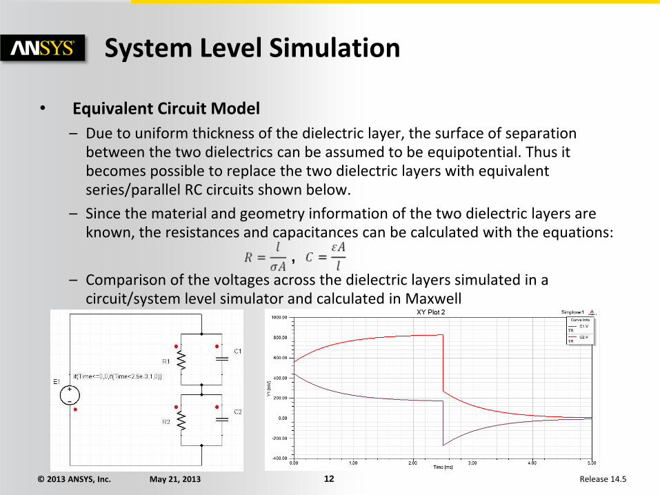
System Level Simulation
• Equivalent Circuit Model
– Due to uniform thickness of the dielectric layer, the surface of separation between the two dielectrics can be assumed to be equipotential. Thus it becomes possible to replace the two dielectric layers with equivalent series/parallel RC circuits shown below.
– Since the material and geometry information of the two dielectric layers are known, the resistances and capacitances can be calculated with the equations:
– Comparison of the voltages across the dielectric layers simulated in a circuit/system level simulator and calculated in Maxwell
,