analysis of frequency selective surfaces …jpier.org/pierb/pierb38/15.11121601.pdf · analysis of...
TRANSCRIPT

Progress In Electromagnetics Research B, Vol. 38, 297–314, 2012
ANALYSIS OF FREQUENCY SELECTIVE SURFACESFOR RADAR ABSORBING MATERIALS
D. Singh1, *, A. Kumar2, S. Meena1, and V. Agarwala2
1Department of Electronics and Computer Engineering, IndianInstitute of Technology Roorkee, Uttrakhand-247667, India2Metallurgical and Materials Engineering Department, Indian Instituteof Technology Roorkee, Uttrakhand-247667, India
Abstract—Nowadays, applications of Frequency Selective Surfaces(FSS) for radar absorbing materials (RAM) are increasing, but it isstill a challenge to select a proper FSS for a particular material as wellas the dimensions of FSS for optimized absorption. Therefore, in thispaper an attempt has been made to optimize the dimensions of FSSfor microwave absorbing application using Genetic Algorithm (GA)approach. The considered frequency selective surfaces are composedof conducting patch elements pasted on the ferrite layer. FSS areused for filtration and microwave absorption. In this work, selectionand optimization of FSS with radar absorbing material has been donefor obtaining the maximum absorption at 8–12 GHz frequency. Anequivalent circuit method has been used for the analysis of differentFSS, which is further used to design fitness function of GA foroptimizing the dimensions of FSS. Eight different available ferritematerials with frequency dependant permittivities and permeabilitieshave been used as material database. The GA optimization is proposedto select the proper material out of eight available materials withproper dimensions of FSS. The optimized results suggest the materialfrom database and dimensions of FSS. The selected material is thenmixed with epoxy and hardener, and coated over the aluminiumsheet. Thereafter, all five FSS were fabricated on ferrite coated Alsheets using photolithographic method followed by wet etching. Theabsorption was measured for all FSS using absorption testing device(ATD) method at X-band. Absorption results showed that significantamount of absorption enhanced with the addition of proper FSS onradar absorbing coating.
Received 16 December 2011, Accepted 17 January 2012, Scheduled 8 February 2012* Corresponding author: Dharmendra Singh ([email protected]).

298 Singh et al.
1. INTRODUCTION
Frequency Selective Surfaces (FSS) are planar periodic structuresof identical patches or apertures of conducting elements repeatingperiodically in either a one or two-dimensional array on a dielectricsubstrate [1–5]. Because of their frequency selective properties,FSS are incorporated in a wide variety of applications such as therealization of reflector antennas, radome design, making polarizersand beam splitters, and also as radar absorbing structure [3, 6–9].Radar Absorbing Materials (RAM) with FSS can improve absorptioncharacteristic as it has combined characteristics of FSS as well asRAM. The frequency behavior of the FSS depends on the shape of theelements (apertures/patches), their size and spacing, and thickness ofthe metal screen. Generally FSS are employed in front of a groundeddielectric slab (substrate) to synthesize high-impedance absorbingsurfaces [3–6, 10, 11].
Incident power absorbed by this type of absorbers generally relieson two aspects: one is by resistive patches (i.e., FSS) and second isdue to the presence of radar absorbing materials. Compared withtraditional RAM coatings, FSS with RAMs have been demonstratedto be lighter, thinner and broadband [2]. However, FSS type RAM’sabsorbing properties are affected by many parameters, such as patchtype, pattern and size, periodicity, and RAM layer’s electromagneticparameters, thickness, etc. Therefore, different FSS shows differentresponse for a particular radar absorbing material. So, it becomesnecessary to investigate the effect of implementing FSS on RAM.
Implementation of FSS on ferrite reduces the thickness of absorberas well as increases the absorption and its physical strength, which ismore favorable for practical applications, but still selection of FSS fora particular RAM is quite challenging. Therefore, there is a needto develop such a technique by which FSS and material selectioncan be done. For this purpose, FSS and material were optimizedthrough genetic algorithm approach. The equivalent transmission linemethod was used to indentify best ferrite material, optimization ofRAM thickness and optimization of different FSS parameters.
This paper is divided into six sections. Section 2 gives briefdetails of FSS analysis. Section 3 defines methodology which includesoptimization of FSS on RAM. Implementation of FSS on RAM coatingis discussed in Section 4. Experimental setup for absorption testing isdiscussed in Section 5. Results and discussion are given in Section 6,followed by conclusion in Section 7.

Progress In Electromagnetics Research B, Vol. 38, 2012 299
2. THEORETICAL ANALYSIS OF FSS
FSS are planar periodic structures that behave like filters toelectromagnetic energy. The available results in literature show thatFSS can modify and improve the absorbing performances of RAM [3].Many materials have been developed for RAM application. In thispaper, an attempt has been made to combine FSS with RAM. Differentelemental shapes of FSS offer different frequency responses. Factorsinfluencing FSS response are:
1. FSS’s element geometry,2. Conductivity of FSS’s material,3. Dielectric substrate to support FSS and4. Incidence angle of the signal.
When electromagnetic energy is incident on a FSS, currents are inducedon the conducting elements. These induced currents then re-radiateEM waves from these conducting elements. Various methods foranalyzing periodic structures have been developed with computationalintensive approaches such as the mutual impedance method [1], themethod of moments (MoM) [12], the finite element method (FEM) [13],the finite-difference time-domain (FDTD) method [4], and EquivalentCircuit (EC) method [4, 14–17]. Out of these, EC method was chosenas it is a simple and powerful technique. Using this technique, FSScan be modeled as energy-storing inductive or capacitive componentswhich are determined by the shape of its elements, but the analysis islimited to linear polarizations and simple FSS element geometries [17].
The configuration of each element (either patch or aperture withinan array of periodic cells), as well as the vertical and horizontalspacings, will contribute to the form of the scattered fields-transmittedor reflected [29]. The basic rule of design is to make the loop
Figure 1. The equivalent circuit approximation of the square loopFSS [17].
300 Singh et al.
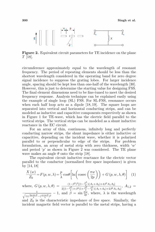
Figure 2. Equivalent circuit parameters for TE incidence on the planeT [18].
circumference approximately equal to the wavelength of resonantfrequency. The period of repeating elements should be less than theshortest wavelength considered in the operating band for zero degreesignal incidence to suppress the grating lobes. For larger incidenceangle, spacing should be kept less than one-half of the wavelength [30].However, this is just to determine the starting value for designing FSS.The final element dimensions need to be fine-tuned to meet the desiredfrequency response. Analysis technique can be explained easily usingthe example of single loop (SL) FSS. For SL-FSS, resonance occurswhen each half loop acts as a dipole [18, 19]. The square loops areseparated into vertical and horizontal conducting strips, and can bemodeled as inductive and capacitive components respectively as shownin Figure 1 for TE-wave, which has the electric field parallel to thevertical strips. The vertical strips can be modeled as a shunt inductivereactance in the EC circuit.
For an array of thin, continuous, infinitely long and perfectlyconducting narrow strips, the shunt impedance is either inductive orcapacitive, depending on the incident wave, whether it is polarizedparallel to or perpendicular to edge of the strips. For problemformulation, an array of metal strip with zero thickness, width ‘w’and period ‘p’ as shown in Figure 2 was considered. The TE planewave makes an angle θ onto the strip [18].
The equivalent circuit inductive reactance for the electric vectorparallel to the conductor (normalized free space impedance) is givenby [14, 18]
X (w)Z0
=F (p, w, λ)=p
λcosθ
[ln
(cosec
(πw
2p
))+ G (p, w, λ, θ)
](1)
where, G (p, w, λ, θ) = (1−β2)2[(1−β4
4)(A1+A2)+4β2A1A2]
2[(1−β2
4)+β2(1+β2
2−β4
8)(A1+A2)+2β6A1A2]
, A1,2 =1√
1± 2p sin θλ
−( p cos θλ
)2− 1, and β = sin πw
2p , where, λ is the wavelength
and Z0 is the characteristic impedance of free space. Similarly, theincident magnetic field vector is parallel to the metal strips, having a

Progress In Electromagnetics Research B, Vol. 38, 2012 301
period ‘p’, and a gap spacing ‘g’ (the electric vector perpendicular tothe conductor has capacitive susceptance), and is incident at an angleof ‘θ’, as shown in Figure 3 [18].
Figure 3. Equivalent circuit parameters for TM incidence on theplane T [18].
Table 1. Equivalent circuit diagram for different FSS.
S.
NoFSS Circuit Equivalent Circuit
Equivalent Inductance
Equivalent Capacitance
1
Single
Square
Loop ),2,(
0
spFp
d
Z
X L 40
Fp
d
Z
Bc
2
Double
Square
Loop
),,( 1
10
spFZ
X L
),,( 2
20
spFZ
X L
4
10
FZ
Bc
4
20
FZ
Bc
3
Triple
Square
Loop
L3
C3
Z0 Z 0L2
C2
L1
C1
),,( 1
10
spFZ
X L
),,( 2
20
spFZ
X L
),,( 3
30
spFZ
X L
4
10
FZ
Bc
4
20
FZ
Bc
430
FZ
Bc
g
s
d
p
Note: All necessary parameter defining FSS are shown in the table.
4Cross
Dipole
L2
C2
Z 0 Z0
L1
C1
),,(0
rL wpF
p
d
Z
X4 F
p
wBg
4 Fp
dBd
5
Jerusalem
Cross
Array 0
Fp
d
Z
X L
),,()2(
4 dppFpgh
Bd
),,(4 gpFp
dBg
p g
d1
w
g
d
h
w
p
= =λ ),,( p λg
=
==
=
),,( p λg
),,( p λg
1
2
=
=
=
λ
λ
λ
λ
λ
),,( p λg1
),,( p λg 2
),,( p λg 3
=
=
=
λ
),,( p λg
),,( p λp-w
=
=
=
-
),,( p λ=
=
=
+λ
λ
( ) w
Reference
[14, 16, 17]
[16, 21, 32]
[16, 20]
[16, 20, 22]
[16, 20, 23]

302 Singh et al.
The capacitive susceptance (normalized free space admittance) iscalculated by
B (g)Z0
= 4F (p, g, λ) (2)
where, ‘g’ is the gap between the conductor and F is function of p, g andλ, which is obtained by replacing ‘w’ by ‘g’ in Eq. (1). The equationspresented above are valid for wavelengths and angles of incidence θ inthe range p(1+sin θ)/λ < 1 and assume that w ¿ p < λ and g ¿ p [18]and are valid for plane wave incident in the E or H plane only. Theequivalent impedance of the SL FSS is given by
Zfss = j
(XL − 1
BC
)(3)
The various FSS structures are considered in the present study, andtheir equivalent circuits are given in Table 1.
2.1. Selection of Substrate for FSS
Generally, dielectric substrates are used to provide structural supportand stabilization to the angular response of FSS [22, 23]. The dielectricsubstrate’s permittivity has a great influence on FSS design. In asingle layer of FSS, FSS is attached to one side of the dielectricsubstrate. The resonant frequency (fr) of FSS array is dependenton the thickness of the supporting dielectric substrate. If the FSS isloaded with thick dielectrics, the resonance frequency is reduced by afactor√εeff [1, 31]. Different FSS/dielectric arrangements will influencethe frequency selective response to a different extent and improve thestability of FSS performance over a range of incident angles. In otherwords, with the use of dielectrics, FSS can be made less sensitive toincident angles.
In the present study, ferrite coated Al sheet was used insteadof dielectric substrate. Ferrites in general are the magnetic oxidesof iron containing magnetic dipoles arranged in a manner whichproduces spontaneous magnetization while maintaining good dielectricproperties, therefore, it can be used as a base material to implementFSS. The electromagnetic energy is dissipated in a ferrite majorly dueto magnetic effect. The loss mechanism in ferrite material dependson the interaction between magnetic vector of electromagnetic waveand the magnetization of the ferrites. In an un-magnetized ferrite themagnetic dipoles are randomly distributed and as a magnetic field isapplied, the magnetic dipoles orientation changes according to type offerrite.
Progress In Electromagnetics Research B, Vol. 38, 2012 303
Meta
l
Z2 Z1
Z(3)Z(2)Z(1)
Meta
l
R
A
M
F
S
S Free space
Reflected wave
Incident wave
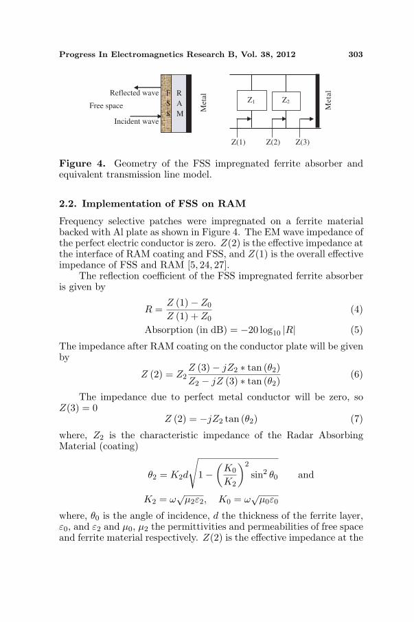
Figure 4. Geometry of the FSS impregnated ferrite absorber andequivalent transmission line model.
2.2. Implementation of FSS on RAM
Frequency selective patches were impregnated on a ferrite materialbacked with Al plate as shown in Figure 4. The EM wave impedance ofthe perfect electric conductor is zero. Z(2) is the effective impedance atthe interface of RAM coating and FSS, and Z(1) is the overall effectiveimpedance of FSS and RAM [5, 24, 27].
The reflection coefficient of the FSS impregnated ferrite absorberis given by
R =Z (1)− Z0
Z (1) + Z0(4)
Absorption (in dB) = −20 log10 |R| (5)
The impedance after RAM coating on the conductor plate will be givenby
Z (2) = Z2Z (3)− jZ2 ∗ tan (θ2)Z2 − jZ (3) ∗ tan (θ2)
(6)
The impedance due to perfect metal conductor will be zero, soZ(3) = 0
Z (2) = −jZ2 tan (θ2) (7)
where, Z2 is the characteristic impedance of the Radar AbsorbingMaterial (coating)
θ2 = K2d
√1−
(K0
K2
)2
sin2 θ0 and
K2 = ω√
µ2ε2, K0 = ω√
µ0ε0
where, θ0 is the angle of incidence, d the thickness of the ferrite layer,ε0, and ε2 and µ0, µ2 the permittivities and permeabilities of free spaceand ferrite material respectively. Z(2) is the effective impedance at the

304 Singh et al.
interface of RAM coating and FSS. Thus impedance at the interfaceof free space and FSS is
Z (1) =Z (2) ∗ Z1
Z (2) + Z1(8)
where, Z1 is the effective impedance of the FSS structure selected andcan be obtained using equivalent impedance as given in Eq. (3) forthe case of single square loop FSS. The equivalent inductance andcapacitance for equivalent circuit which were used for optimizationare given in Table 1. These equivalent inductance and capacitanceare further utilized to find Zfss as Eq. (3) by which the calculation ofreflection loss can be computed using Eqs. (4) and (5).
3. METHODOLOGY: OPTIMIZATION OF FSS ON RAM
There are many physical parameters needed to be determined, suchas proper ferrite material (i.e., proper permittivity, permeability) andthickness of ferrite coating as well as shape (i.e., periodicity, gap andwidth) of FSS structure (which defines inductance and capacitanceof the structure by which resultant impedance can be calculated).GA was used as an optimization technique to optimize the variousparameters such as periodicity ‘p’, gap ‘g’, width ‘s’, ferrite material‘m’ and thickness of ferrite coating ‘t’, as GA is very powerful forproblems that have a large number of variables [28]. All dimensionsconsidered are in meter. Frequency selective surfaces for the radarabsorbing material were designed for single layer RAM coating withFSS impregnated on it. To replicate mathematically the FSS for RAM,the transmission line equivalent method as discussed in Subsection 2.2was used. Five different FSS as shown in Table 1 were criticallyanalyzed for the absorption purpose at X-band. The eight types offerrite material (details given in Table 2) were used for optimization.The corresponding permittivity and permeability of these materials atdifferent frequencies are listed in Table 2. According to change in thevalue of α and β, µ and ε may be computed for different frequenciesat X-band [25, 30].
So, it is important to select proper material from database withsuitable FSS for better absorption at X-band. Therefore, for thispurpose GA optimization has been used and details are given inFigure 5(a).

Progress In Electromagnetics Research B, Vol. 38, 2012 305
4. IMPLEMENTATION OF FREQUENCY SELECTIVESURFACES ON RAM COATING
The genetic algorithm is an iterative optimization procedure that startswith a randomly selected population of potential solution and generallyevolve towards better solutions through the application of geneticoperator. Their repetitive applications to the population of potentialsolutions result in an optimization process that resembles naturalevolution. The three genetic operator governing the iterative search areoften referred to as the selection, cross-over and mutation operators.The probabilistic nature of all the three operators greatly enhancethe capabilities of the algorithm to search for a global rather thanlocal fitness function. The flow chart of GA optimization technique isshown in Figure 5(b). The Fitness function for optimizing Eq. (5) with
Table 2. Material database used for optimization [25].
f
GHzf
rr
(8
, f
GHzf
i
i
8,
S No
Material (8GHz) (8GHz) (8GHz) (8GHz)
1 Ba(MnTi)1.7Fe8.6O19
5.63
0.019252
2.41
0.049792
0.12
-0.08951
2.5
0.036445
2 Ba(MnTi)1.8Fe8.4O19
2.99
-0.01396
3.24
0.045507
1.73
0.021888
0.2
-0.08288
3 Ba(MnTi)1.9Fe8.2O19
3.99
-0.00243
1.84
0.02929
1.14
-0.01273
1.26
0.002088
4 SrZn1.2Fe13.2Sn0.6Mn0.6O23.8
2.67
-0.02174
0.7
0.00585
0.091
-0.08504
1.795
0.004794
5 BaTiO3
3.325
-0.00369
13.65
0.059571
1
0
0
0
6 Ba(MnTi)3.5Fe5.0O19
6.485
0.022805
3.816
0.056184
1.893
0.027582
0.04
-0.13677
7 Ba(MnTi)1.6Fe8.8O19
7.08
0.036194
0.36
0.03738
1.92
0.022261
1.15
0.02103
8 Ba(Mn0.15 Co0.85)2Fe16O27
8.837
0.010656
1.84
0.00826
0.745
0.009302
2.015
0.020206
ε ε( )= ε ( )=
εα β
)
f
GHzf
rr
(8( )=
α
)µ
µ( )
f
GHzf
i
i
8( )= β
( ), µ
µ
rε iε rµ
α αβ β
iµ

306 Singh et al.
Select a unit cell of desired FSS
Geometry of FSS is defined mathematically
in terms of variables
Draw the equivalent circuit of FSS structure
Calculate the impedance of equivalent circuit using q 3 in
terms of already defined variables
Impedance of ferrite layer at FSS interface was calculated
using q. 6 and q. 7
Impedance at FSS and free space interface was
calculated using q. 8
Calculation of reflection coefficient
(Fitness Function )
Fitness function F (p, g, s, m and t) was
optimized using Genetic Algorithm
E .
E E
E
)( ) (
( )
)(
Start
Construct initial population
Fitness scaling
Selection phase
Crossover phase
Mutation phase
Convergence checkNo
Yes
Stop
(a) (b)
Figure 5. Steps used before optimization to FSS on RAM (a) andflow chart of genetic algorithm (b).
different equations as shown in column 3 and 4 of Table 1 were usedand the fitness function was optimized using “gatool” of MATLABwith different parameters. The optimized results for single square loopFSS i.e., gap between patches ‘g’, width of patch ‘s’, length of thepatch ‘d’, material ‘m’ (Ba(MnTi)1.6Fe8.8O19) and the thickness offerrite coating ‘t’ are shown in Table 3. Period ‘p’ depends on thevalues of ‘g’ and ‘d’, hence it is not shown. In the same way variablesfor other FSS are also shown; not shown variables can be inferred fromshown variables. Double square and triple square loop FSS being morecomplex geometry require more parameters to define geometry.
For simplicity and comparison of all FSS, all Al sheets were coatedwith the material Ba(MnTi)1.6Fe8.8O19 for 0.2 mm thickness, as itwas not possible to spray coat Al sheets for the dimension optimizedthrough GA. The ferrite coating was dried for more than 8–10 h. A thin

Progress In Electromagnetics Research B, Vol. 38, 2012 307
Collect the dimension of selected FSS element and thickness of ferrite after optimization of the FSS for RAM
Ferrite paint was coated on Al sheet with optimized thickness
Make an exact drawing of FSS with optimized
dimension in AUTO-CAD
Take printout on transparency sheet (non-metallic area
should be complete dark )
Fix the copper foil on RAM coated Al sheet
Photolithography method was used to fabricate
FSS of copper foil
Figure 6. Flow chart to fabricate FSS on RAM.
copper foil was stacked on RAM coated Al sheet by applying a verythin layer of epoxy based adhesive (Araldite) between both surfaces(i.e., copper foil and RAM coated Al sheet) and then a pressure wasapplied, by which adhesive layer thickness becomes nearly zero. Thedetails of fabrication are given in flow chart shown in Figure 6. Thecomplete structure had been then dried for 48 h.
5. EXPERIMENTAL SETUP
The absorption properties of designed FSS have been measured byingeniously developed Absorption Testing Device (ATD) at 8–12 GHz.Details are shown in Figure 7 [26]. A 2 mm thick 94.5 × 74.2 mm2
Al sheet was used for coating ferrite material and fabricating FSSon it, which was used in ATD for absorption testing. In order tomeasure absorption from ATD, power reflected from coated samplewas subtracted from power reflected from uncoated sample.

308 Singh et al.
(a)
(b)
Figure 7. (a) Schematic diagram of Absorption Testing Device (ATD)and (b) experimental setup for absorption measurement.
Table 3. Optimized results for different FSS.
S
NoFSS Optimized Dimension (in meter)
g s d m t
1
Single Square
loop 0.00427 0.00054 0.00181 7 0.00039
g1 g2
s1 s2
d2 m t
2
Double
Square
loop 0.00142 0.0010 0.00051 0.00098 0.00609 7 0.00040
g1 g2
g3 s1 s2 s3 d2 m t
3Triple
Square
loop 0.00182 0.00127 0.00160 0.00169 0.00193 0.00072 0.00864 7 0.00039
g w d m t 4
CrossDipole
0.00956 0.00782 0.01470 7 0.00047
g w d h p m t 5
Jerusalemcross
0.00473 0.00286 0.00848 0.00044 0.01336 7 0.00043

Progress In Electromagnetics Research B, Vol. 38, 2012 309
6. RESULTS AND DISCUSSION
The objective of this paper was to select a ferrite material out ofavailable ferrite materials and to determine the FSS with variousparameters, such as periodicity, gap, and width. The implementationhas been done as discussed in Section 4, and the results of optimizationare shown in Table 3. Absorption characteristics of ferrite coating,with and without FSS (as considered in Table 1) were checked usingAttenuation Testing Device (ATD). Firstly, Al sheet was coatedwith Ba(MnTi)1.6Fe8.8O19 (material No. 7 Table 2 as obtained fromoptimized results) as shown in Figure 8(a) and its ATD result is shownin Figure 8(b). It is observed from Figure 8(b) that the ferrite coatedAl sheet has maximum absorption of 0.58 dB at 10.5 and 11 GHz.
(a)
(f)(e)
(d)(c)
(b)
Single Layer
Ferrite Coating
Single Square
FSS
Double Square
FSS
Frequency (GHz)

310 Singh et al.
(l)(k)
(i)
(g)
Triple SquareFSS
Cross Dipole
Jerusalem CrossFSS
FSS
(j)
(h)
Figure 8. Effect of different FSS on microwave absorption on normalincidence.
After that a single square FSS was fabricated over Ba(MnTi)1.6Fe8.8
O19 ferrite, as shown in Figure 8(c). In this graph, maximum 2 dB ab-sorption was observed at 9GHz and 10.5 GHz, as shown in Figure 8(d).The enhancement in absorption may be due to the interaction betweenmicrowave with conducting copper and ferrite material which may leadto more internal reflections [29].
In another ferrite coated Al sheet, a double square FSS (as givenin Table 1, serial No. 2) was fabricated, which is shown in Figure 8(e).Figure 8(f) shows corresponding absorption behavior and in this casemaximum 4.99 dB absorption was observed at 10 GHz frequency.
Figure 8(g) shows triple square FSS (as shown in Table 1, serialNo. 3), and corresponding absorption behavior is shown in Figure 8(h).

Progress In Electromagnetics Research B, Vol. 38, 2012 311
A maximum absorption of 9.19 dB at 10 GHz was observed.Figures 8(i) and (k) show Cross Dipole and Jerusalem FSS
respectively (as shown in Table 1, serial Nos. 4 and 5) andcorresponding absorption behavior are shown in Figures 8(j) and (l).It was observed that the maximum absorption in case of Cross DipoleFSS was 5.22 dB at 9GHz and a maximum absorption of 4.86 dB at9GHz & 10.5 GHz in case of Jerusalem Cross FSS was observed.
The results shown in Figures 8(b), (d), (f), (h), (j) and (l)suggest that the implementation of different FSS on ferrite coatedAl sheet increases the absorption amount. The maximum absorptionwas observed in case of triple square FSS in comparison to the otherconsidered FSS. It can be inferred that the amount of absorption willbe enhanced significantly with the use of triple square FSS withoutchanging the thickness of the coating at selected X-band.
7. CONCLUSION
The dimensions of the perfect conducting FSS, and RAM’s thicknesswere optimized using genetic algorithm. The structure preparedin this work presents proper characteristics for handling, flexibilityand lightweight, meeting requirements for its application. Anotherimportant advantage of the processed FSS on RAM is its low specificmass compared to single ferrite coating.
The ferrite paint was coated on an Al sheet, and the FSS wasimplemented on it with optimized dimensions and then tested usingATD (X-band). It has been observed from ATD testing that maximumattenuation was found in case of triple square frequency selectivesurfaces. Implementation of FSS on coated Al sheet has shownencouraging results. The results show the enhancement in absorptionwith the addition of FSS on RAM. This type of analysis helps inreducing thickness of the radar absorbers and in selecting proper FSSand RAM for the given application.
REFERENCES
1. Munk, B. A., Frequency Selective Surfaces — Theory and Design,John Wiley and Sons, Inc., New York, 2000.
2. Wu, T. K., Frequency Selective Surfaces and Grid Array, JohnWiley and Sons, Inc., New York, 1995.
3. Liu, H. T., H. F. Cheng, Z. Y. Chu, et al., “Absorbing propertiesof frequency selective surface absorbers with cross-shaped resistivepatches,” Material Design, Vol. 28, 2166–2171, 2007.

312 Singh et al.
4. Mias, C., C. Tsakonas, and C. Oswald, “An investigation intothe feasibility of designing frequency selective windows employingperiodic structures, (Ref. AY3922),” Tech. Rep., Final Report forthe Radio-communications Agency, Nottingham Trent University,2001.
5. Sakran, F. and Y. Neve-Oz, “Absorbing frequency-selective-surface for the mm-wave range,” IEEE Transactions on Antennasand Propagation, Vol. 56, No. 8, 2649–2655, 2008.
6. Arya, F., M. Matthew, H. Christian, and V. Rudiger, “Efficientprocedures for the optimization of frequency selective surfaces,”IEEE Transactions on Antennas and Propagation, Vol. 56, No. 5,1340–1349, 2008.
7. Munk, B. A., R. J. Luebbers, and R. D. Fulton, “Transmissionthrough a two-layer array of loaded slots,” IEEE Transactions onAntennas and Propagation, Vol. 22, 804–809, 1974.
8. Ulrich, R., “Far-infrared properties of metallic mesh and itscomplementary structure,” Infrared Physics, Vol. 7, 37–55, 1967.
9. Durschlag, M. S. and T. A. DeTemple, “Far-IR optical propertiesof freestanding and dielectrically backed metal meshes,” AppliedOptics, Vol. 20, 1245–1253, 1981.
10. Chen, H. Y., X. Y. Hou, and L. J. Deng, “A novel microwaveabsorbing structure using FSS metamaterial,” PIERS Proceedings,1195–1198, Moscow, Russia, Aug. 18–21, 2009.
11. Simms, S. and V. Fusco, “Tunable thin radar absorber usingartificial magnetic ground plane with variable backplane,”Electronics Letters, Vol. 42, No. 21, 1197–1198, 2006.
12. Kominami, M., H. Wakabayashi, S. Sawa, and H. Nakashima,“Scattering from a periodic array of arbitrary shaped elementson a semi infinite substrate,” Electronics and Communications inJapan (Part I: Communications), Vol. 77, No. 1, 85–94, 1994.
13. Bardi, I., R. Remski, D. Perry, and Z. Cendes, “Plane wavescattering from frequency-selective surfaces by the finite-elementmethod,” IEEE Transactions on Magnetics, Vol. 38, No. 2, 641–644, 2002.
14. Langley, R. J. and E. A. Parker, “Equivalent circuit model forarrays of square loops,” Electronic Letters, Vol. 18, No. 7, 294–296, 1982.
15. Lee, C. K. and R. J. Langley, “Equivalent-circuit models forfrequency-selective surfaces at oblique angles of incidence,” IEEProceeding H, Vol. 132, No. 6, 395–399, 1985.
16. Dubrovka, R., J. Vazquez, C. Parini, and D. Moore, “Equivalent

Progress In Electromagnetics Research B, Vol. 38, 2012 313
circuit method for analysis and synthesis of frequency selectivesurfaces,” IEE Proceeding on Microwave Antennas Propagation,Vol. 153, No. 3, 213–220, 2006.
17. Sung, G. H., K. W. Sowerby, and A. G. Williamson, “Equivalentcircuit modelling of a frequency selective plasterboard wall,” IEEEAntennas and Propagation Society International Symposium,Vol. 4A, 400–403, 2005.
18. Philippakis, M., C. Martel, D. Kemp, S. Appleton, andS. Massey, “Application of FSS structures to selectively controlthe propagation of signals into and out of buildings annex 3:Enhancing propagation into buildings,” Final Report, ERAProject 51-CC-12033, ERA Report, 2004.
19. Campos, A. L. P. D. S., “Analysis of frequency selective surfaceswith metallic and dielectric losses at millimeter wave range,” Int.J. Infrared Milli Waves, Vol. 29, 684–692, 2009.
20. Kumar, R., “Study and characterization of Zn-Mn and Zn-Coferrite using FSSs at microwave frequency”, ME Dissertation inElectronics and Communication Engineering, Department of E. &C., IIT Roorkee, Mar. 1998.
21. Langley, R. J. and E. A. Parker, “Double-square frequency-selective surfaces and their equivalent circuit,” Electronics Letters,Vol. 19, No. 17, 675–677, 1983.
22. Kiani, G. I., A. R. Weily, and K. P. Esselle, “Frequency selectivesurface absorber using resistive cross-dipoles,” IEEE Antennasand Propagation Society International Symposium, 4199–4202,2006.
23. Langley, R. J. and A. J. Drinkwater, “Improved empirical modelfor the jerusalem cross,” Microwaves, Optics and Antennas, IEEProceedings H, Vol.129, No. 1, 1–6, 1982.
24. Huiling, Z., G. B. Wan, and W. Wan, “Absorbing properties offrequency selective surface absorbers on a lossy dielectric slab,”PIERS Proceedings, 165–168, Beijing, China, Mar. 23–27, 2009.
25. Parida, R. C., D. Singh, and N. K. Agarwal, “Implementation ofmultilayer ferrite radar absorbing coating with genetic algorithmfor radar cross-section reduction at X-band,” Indian Journal ofRadio & Space Physics, Vol. 36, No. 2, 145–152, 2007.
26. Meshram, M. R., N. K. Agrawal, B. Sinha, and P. S. Misra,“A study on the behaviour of M-type barium hexagonal ferritebased microwave absorbing paints,” Bulletin of Materials Science,Vol. 25, No. 2, 169–173, 2002.
27. Park, K. Y., S. E. Lee, C. G. Kim, and J. H. Han, “Fabrication and
314 Singh et al.
electromagnetic characteristics of electromagnetic wave absorbingsandwich structures,” Composites Science and Technology,Vol. 66, 576–584, 2006.
28. Kern, D. J. and D. H. Werner, “A genetic algorithm approachto the design of ultra-thin electromagnetic bandgap absorbers,”Microwave and Optical Technology Letters, Vol. 38, No. 1, 61–64,2003.
29. Folgueras, L. d. C., E. L. Nohara, R. Faez, and M. C. Rezende,“Dielectric microwave absorbing material processed by impregna-tion of carbon fiber fabric with polyaniline,” Materials Research,Vol. 10, No. 1, 95–99, 2007.
30. Sugimoto, S., S. Kondo, K. Okayama, H. Nakamura, D. Book,T. Kagotani, and M. Homma, “M-type ferrite composite asa microwave absorber with wide bandwidth in GHz,” IEEETransactions on Magnetics, Vol. 35, No. 5, 3154–3156, 1999.
31. Filippo, C., A. Claudio, M. Agostino, and E. Prati, “Waveguidedielectric permittivity measurement technique based on resonantFSS filters,” IEEE Microwave and Wireless Components Letters,Vol. 21, No. 5, 273–275, 2011.
32. Luo, X. F., P. T. Teo, A. Qing, and C. K. Lee, “Design of double-square-loop frequency-selective surfaces using differential evolu-tion strategy coupled with equivalent-circuit model,” Microwaveand Optical Technology Letters, Vol. 44, No. 2, 159–162, 2005.