analysis and design of a scalable digital input class d ... · pdf fileanalysis and design of...
TRANSCRIPT
ANALYSIS AND DESIGN OF A SCALABLE DIGITAL INPUT
CLASS D AUDIO AMPLIFIER TOPOLOGY
ByAnthony Forzley, B. Sc., M. Sc.
A thesis subm itted to the
Faculty of Graduate and Postdoctoral Affairs
in partial fulfillment of the requirements for the degree of
DOCTOR OF PHILOSOPHY
in
ELECTRICAL AND COM PUTER ENGINEERING
Ottawa-Carleton Institute for Electrical and Computer Engineering
Carleton University
Department of Electronics
© Anthony Forzley, 2013

1+1Library and Archives Canada
Published Heritage Branch
Bibliotheque et Archives Canada
Direction du Patrimoine de I'edition
395 Wellington Street Ottawa ON K1A0N4 Canada
395, rue Wellington Ottawa ON K1A 0N4 Canada
Your file Votre reference
ISBN: 978-0-494-94215-4
Our file Notre reference ISBN: 978-0-494-94215-4
NOTICE:
The author has granted a nonexclusive license allowing Library and Archives Canada to reproduce, publish, archive, preserve, conserve, communicate to the public by telecommunication or on the Internet, loan, distrbute and sell theses worldwide, for commercial or noncommercial purposes, in microform, paper, electronic and/or any other formats.
AVIS:
L'auteur a accorde une licence non exclusive permettant a la Bibliotheque et Archives Canada de reproduire, publier, archiver, sauvegarder, conserver, transmettre au public par telecommunication ou par I'lnternet, preter, distribuer et vendre des theses partout dans le monde, a des fins commerciales ou autres, sur support microforme, papier, electronique et/ou autres formats.
The author retains copyright ownership and moral rights in this thesis. Neither the thesis nor substantial extracts from it may be printed or otherwise reproduced without the author's permission.
L'auteur conserve la propriete du droit d'auteur et des droits moraux qui protege cette these. Ni la these ni des extraits substantiels de celle-ci ne doivent etre imprimes ou autrement reproduits sans son autorisation.
In compliance with the Canadian Privacy Act some supporting forms may have been removed from this thesis.
While these forms may be included in the document page count, their removal does not represent any loss of content from the thesis.
Conformement a la loi canadienne sur la protection de la vie privee, quelques formulaires secondaires ont ete enleves de cette these.
Bien que ces formulaires aient inclus dans la pagination, il n'y aura aucun contenu manquant.
Canada

Acknowledgem ents
This thesis could not have been accomplished without the help and support of my research advisor
Professor Ralph Mason. His advice and guidance during the past several years was essential in
completing this thesis. Ralph has been a good friend throughout this long and arduous process.
For that, I am very thankful.
I would like to thank the examination committee members Dr. Florinel Balteanu of Skyworks
Solutions, Professor Emad Gad, University of Ottawa, Professor Halim Yanikomeroglu, Depart
ment of Systems and Computer Engineering, Professor Calvin P lett, Department of Electronics
and Professor Maitham Shams, Department of Electronics. Their time and comments are greatly
appreciated.
I would also like to thank Yasser Soliman for technical support with various Cadence and
Latex issues. Your help spared me a lot of frustration and ultimately saved me much time.
Scholarships from the National Science and Engineering Research Council, Carleton University
and Dept, of Electronics are gratefully acknowledged. W ithout the financial assistance I could not
of returned to graduate school. In addition, I would like to thank the Canadian Microelectronics
Corporation for their fabrication services and test equipment support.
Finally, a big thank you to my family Sandra, Maxwell and Alexander who were wondering
if this day would ever come.
A bstract
A digital input Class D audio amplifier is investigated in this thesis. The intended application
is headphone enabled portable audio players such as sm art phones and tablets. The topology
is intended to be predominately digital and thereby allow for rapid scaling in deep submicron
CMOS processes. Class D was chosen for its natural compatibility with pulse modulation schemes
and theoretical 100% efficiency. Current Class AB amplifiers offer very good audio quality but
generally poor efficiency.
The Class D amplifier with global feedback was prototyped with a Field Programmable Gate
Array (FPGA) and commercial 16b Analog to Digital converter (ADC). Measurement and sim
ulation results indicate stable operation with greater than 30 dB of noise rejection a t 1 kHz. A
revised design operating a t a lower frequency with improved noise rejection was simulated.
An integral component of the topology is the 2.82 Msps 16b ADC. To meet the power specification
of <5 mW a unique variant of the successive approximation algorithm termed the Configurable
Offset with Preamplifier (COP) ADC was developed. The core of the ADC consists of a pream
plifier array and latched comparator. Intentional mismatches are introduced to produce voltage
references for the conversion process and thereby eliminating the need for a Digital to Analog
Converter (DAC). The core circuits of the COP ADC were implemented in 0.13/xm CMOS. The
COP ADC required external digital control and clocks via a FPGA. A passive charge sharing
sample and hold circuit and calibration algorithm are also required for a complete solution.
Both AC and DC automated measurements yield 13.8b resolution over a 293 mVpp operating
range and 6.25 MHz comparator clock. The maximum INL=0.5 LSB, DNL=1 LSB and core
power consumption of 1.5 mW. In addition, gain and rejection ratio formulas for a asymmetric
differential pair amplifier were derived and correlated well with simulation results.

Table of Contents
Acknowledgements ii
Abstract iii
Table of Contents iv
List o f Tables viii
List of Figures ix
List o f Abbreviations and Sym bols xiii
1 Introduction 11.1 Motivation ................................................................................................................................. 21.2 O bjectives.................................................................................................................................... 31.3 C on tribu tions.............................................................................................................................. 31.4 O rg a n iz a tio n .............................................................................................................................. 5
2 Background 62.1 Digital Audio S o u rce ................................................................................................................. 72.2 M odu la to r.................................................................................................................................... 7
2.2.1 Pulse W idth M odulation............................................................................................ 82.2.2 Sigma-Delta M odulation ............................................................................................ 12
2.3 Digital to Analog C o n v e rte r................................................................................................... 142.4 Power Amplifier........................................................................................................................... 14
2.4.1 Linear A m plifiers......................................................................................................... 142.4.2 Switching Mode Power Amplifiers .......................................................................... 16
2.5 S peakers........................................................................................................................................ 172.6 Power Amplifier Efficiency....................................................................................................... 19
2.6.1 Definitions ................................................................................................................... 192.6.2 Linear Power Amplifier Efficiency............................................................................. 202.6.3 Class-D E ffic ie n c y ...................................................................................................... 23
2.7 Key Points ................................................................................................................................. 29
iv

3 Audio Amplifier Technology Review 313.1 System Specifications..................................................................................................................... 313.2 Sources of D is to rtio n ................................................................................................................. 333.3 Linearization Techniques.......................................................................................................... 34
3.3.1 Negative F e e d b a c k ....................................................................................................... 353.3.2 Alternative Linearization Techniques............................................................................ 38
3.4 Switching Mode Audio Amplifiers.......................................................................................... 393.4.1 Switching Mode Power Amplifier C ategories............................................................... 40
Category I ................................................................................................................... 40Category I I ................................................................................................................... 42Category III ................................................................................................................ 45Category I V ................................................................................................................... 46Category V ................................................................................................................... 47
3.4.2 Commercial Class-D A m plifiers................................................................................. 483.5 Key Points ................................................................................................................................. 49
4 System Design 504.1 System A rc h ite c tu re ................................................................................................................. 50
4.1.1 Interpolation F i l t e r s .................................................................................................... 534.1.2 D P W M ........................................................................................................................... 54
Sigma Delta M odulation ............................................................................................ 54Modulation Index ...................................................................................................... 57MASH 1-2 Sim ulations................................................................................................ 57P W M ............................................................................................................................. 60Multi-bit Selection C r i t e r i a ...................................................................................... 60
4.2 Control Loop A n a ly s is .............................................................................................................. 614.2.1 Continuous to Discrete T i m e ..................................................................................... 63
4.3 System P ro to ty p e ........................................................................................................................ 644.3.1 Bode Plot A nalysis....................................................................................................... 664.3.2 A D C .................................................................................................................................. 684.3.3 S im u la tio n s ..................................................................................................................... 684.3.4 Measurements .............................................................................................................. 68
4.4 Revised System D esign .............................................................................................................. 714.4.1 Interpolation F i l t e r s .................................................................................................... 724.4.2 PID C o m p e n sa to r ........................................................................................................ 734.4.3 S im u la tio n s ..................................................................................................................... 75
4.5 CMOS Class D ..............................................................................................................................804.5.1 Switching losses.................................................................................................................. 804.5.2 Conduction losses ............................................................................................................824.5.3 Total lo s s e s .........................................................................................................................83
4.6 Key Points ................................................................................................................................. 84
v

5 Low Power ADC Design 855.1 SAR A lg o rith m ........................................................................................................................ 855.2 COP ADC A rc h ite c tu re ........................................................................................................ 89
5.2.1 Track-and-H old................................................................................................................. 915.2.2 P ream plifier.................................................................................................................... 91
Gain and Rejection R a tio s .......................................................................................... 92Offset V oltage................................................................................................................ 96Noise ............................................................................................................................. 97Preamplifier Array Analysis and S im u la tio n s ...................................................... 98
5.2.3 C o m p ara to r......................................................................................................................102Latched C o m p ara to r.....................................................................................................104Offset C onfigura tion .....................................................................................................106Comparator N o i s e ........................................................................................................ 110
5.3 Cascaded P erfo rm ance..............................................................................................................I l l5.3.1 Tuning R an g e ...................................................................................................................I l l5.3.2 Cascaded N o ise ............................................................................................................... 112
5.4 Key Points ................................................................................................................................. 115
6 ADC Test and M easurements 1176.1 Integrated Circuit O verview ....................................................................................................1176.2 Digital Interface ....................................................................................................................... 1176.3 Measurement S y stem .................................................................................................................121
6.3.1 Printed Circuit B o a r d .................................................................................................. 1216.3.2 Automated T esting .........................................................................................................122
DC M easu rem en ts ........................................................................................................ 122AC M easu rem en ts ........................................................................................................123
6.4 Measurement R esu lts .................................................................................................................1246.4.1 DC M easu rem en ts .........................................................................................................124
H y ste resis ........................................................................................................................ 1256.4.2 AC M easu rem en ts .........................................................................................................128
Noise ...............................................................................................................................1316.5 Comparison Table .................................................................................................................... 135
6.5.1 Quiescent Power E s tim a te ............................................................................................1356.5.2 Maximum System Efficiency.........................................................................................1376.5.3 Other Parameters ......................................................................................................... 137
6.6 Key Points ................................................................................................................................. 137
7 Conclusions 1397.1 Future Work ..............................................................................................................................140
A ppendix A M ism atch in differential amplifiers 142
Appendices 142
vi

Appendix B PC B CAD
Bibliography

List of Tables
2.1 Conduction angles and efficiency ratings for linear mode amplifiers.............................. 15
3.1 Low power digital audio system specifications..................................................................... 32
3.2 Overview of current switching mode audio power amplifier techniques.............................40
5.1 Initial COP ADC target specifications................................................................................... 91
5.2 Preamplifier array device param eters(Vcc=1.2V, R = 75012 and Ibias=L25m A). . . . 99
5.3 Latched comparator device sizes................................................................................................104
5.4 Comparator mismatched device sizes........................................................................................108
6.1 Pinout with description................................................................................................................ 119
6.2 Config register settings for programmable offsets..................................................................120
6.3 DC Measured input referred offset resolution and tuning range........................................125
6.4 Measured input referred offset resolution and tuning range............................................... 131
6.5 Noise measurements...................................................................................................................... 133
6.6 Published specifications for digital input Class D audio amplifiers. All power spec
ifications are for single channel mono operation................................................................... 136

List of Figures
2.1 Digital audio system block diagram....................................................................................... 6
2.2 Natural sampling PW M (NPWM) circuit............................................................................ 8
2.3 PWM waveforms for the natural sampling (NPWM) and uniform sampling (UPWM)
processes........................................................................................................................................ 9
2.4 Second and third order harmonic distortion relative to fundamental with M = l. . . 11
2.5 Direct digital conversion PCM to P W M ............................................................................ 12
2.6 First order Sigma-Delta modulator: a) System block diagram, b) Input and output
time domain waveforms, c) Noise shaped spectral ou tpu t....................................................13
2.7 Basic circuit configuration of a single ended Class A, AB, B or C amplifier...................15
2.8 Current-Voltage plane operating locus of different power amplifier classes......................16
2.9 Headphone impedance measurement of Sony MDR-E8181.............................................. 18
2.10 Speaker connection configurations, a) single ended, b) differential or BTL..................... 18
2.11 Maximum theoretical collector efficiency r?c versus conduction angle................................20
2.12 Normalized maximum power output capability versus conduction angle......................... 21
2.13 Collector efficiency r)c of ideal Class-A, B, G2 (a=0.5) amplifiers......................................22
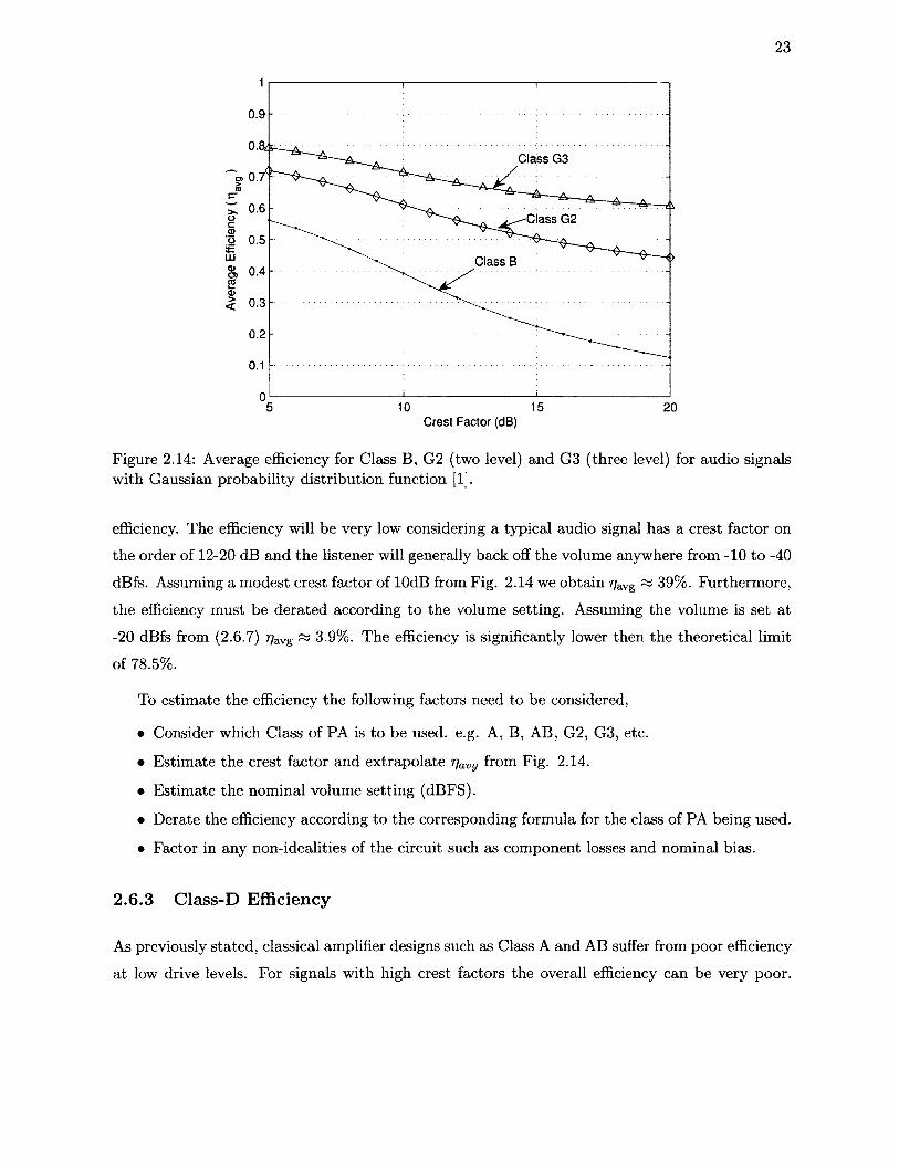
2.14 Average efficiency for Class B, G2 (two level) and G3 (three level) for audio signals
with Gaussian probability distribution function [1]........................................................... 23
2.15 Class D circuit: (a) MOS circuit schematic, (b) equivalent ideal circuit.......................... 24
2.16 Voltage and current waveforms in an ideal Class D switching mode amplifier a)
voltage V2 a t the input to the load network, b) resistor voltage vQ, c) Q\ drain
current ii , d) Q 2 drain current *2 , e) resistor current i0....................................................... 26
2.17 Switching amplifier with various load networks...................................................................... 27
2.18 Switching mode amplifier efficiency calculation for various load networks. Resonant
frequency 1 MHz, R=16 fi, L=1 mH and C=25.3 n F ...........................................................29
ix

3.1 A-Weighted filter response commonly used in audio measurements.................................33
3.2 Closed loop control system..........................................................................................................35
3.3 Sample and hold delay.............................................................................................................. 38
3.4 Pulse modulation system with feedback................................................................................... 39
3.5 Block diagrams of different Class D categories....................................................................... 41
3.6 Pulse edge detection and correction system.............................................................................43
4.1 Block diagram of the Class D amplifier w ith digital compensation................................... 51
4.2 Input and output spectrum of an ideal interpolation filter...................................................53
4.3 EA SNR calculations for L=1 to 4 with M =2....................................................................... 55
4.4 Sigma-Delta MASH 1-2 block diagram................................................................................ 56
4.5 MASH 1-2 time domain plots for a 10 kHz input with a sample rate of 400ns
(OSR=62.5): a) O utput of the first order sigma-delta, b) Output of the second
order sigma-delta, c) Overall third order noise shaped output obtained from the
sum of plots a and b ................................................................................................................... 58
4.6 Nine level MASH 1-2 SNR plot. M atlab simulation with 1 kHz tone and k = l/2 . . 59
4.7 PWM parallel to serial conversion process.......................................................................... 60
4.8 Feedback compensation model a) Continuous time model, b) Mixed signal model
digital re d e s ig n .......................................................................................................................... 62
4.9 Forward and reverse noise injection loop a n a ly s is .......................................................... 63
4.10 Prototype hardware and measurement implementation.................................................. 64
4.11 FPGA prototype open loop frequency response assuming H (s)= l and P (s )= l . . . 66
4.12 FPGA prototype closed loop frequency response assuming H (s)= l and P (s )= l . . 67
4.13 FFT plot at the output of the MASH 1-2 and differential LPF. Plot obtained with
f s=2.5 MHz and applying a hanning window..................................................................... 69
4.14 Frequency response of the control loop compensation..........................................................70
4.15 FPGA PW M output as measured on a HP3585A spectrum analyzer (-6dBfs, 20
Hz-22 kHz, lO dB/div)................................................................................................................ 70
4.16 Block diagram for revised system with reduced operating frequency. .......................... 71
4.17 Block diagram of OSR=32 interpolation filter a) Baseband input spectrum, b)
Halfband FIR 2x, c) LPF FIR 4x, d) S/H 4x, e) cascaded output................................ 73
4.18 Interpolation Filter frequency response, a) Baseband input spectrum, b) Halfband
FIR 2x, c) LPF FIR 4x, d) S/H 4x, e) cascaded ou tpu t.......................................................74
x

4.19 Revised design open loop frequency response, H (s)= l and P ( s ) = l ............................... 76
4.20 Revised design closed loop frequency response, H (s)= l and P ( s ) = l ............................77
4.21 Revised design closed loop mixed signal Simulink model SNR.................................... 78
4.22 Revised design closed loop spectral ou tpu t....................................................................... 79
4.23 Revised design forward path noise suppression....................................................................79
4.24 Class D amplifier consisting of a driver and power stage.................................................... 80
4.25 Simulation of Class D amplifier, a) Average 10% to 90% rise/fall time, b) Energy
per switching cycle...................................................................................................................... 82
4.26 Total switching losses of the driver and power stage as a function of frequency. . . 83
5.1 SAR ADC algorithm f lo w c h a r t ........................................................................................... 87
5.2 Conventional and alternative SAR ADC block diagrams................................................ 88
5.3 COP SAR ADC block d ia g ra m ........................................................................................... 89
5.4 Differential amplifier................................................................................................................. 92
5.5 Source coupled differential pair amplifier.................................................................................95
5.6 Simplified model for low and moderate frequencies with zero gate current..................... 98
5.7 Preamplifier schematic..................................................................................................................99
5.8 Preamplifier simulated and calculated a) differential gain A dm, b) rejection ratios
for the preamplifier a r r a y . ........................................................................................................ 101
5.9 Preamplifier simulated and calculated normalized rejection ratios................................. 102
5.10 Preamplifier simulated and calculated input referred offsets............................................ 103
5.11 Preamplifier simulated input referred noise.......................................................................... 103
5.12 Comparator with variable and fixed reference voltages......................................................104
5.13 Latch type voltage sense amplifier [2].....................................................................................105
5.14 Transient response of the output nodes during reset and compare clock phases. . . 106
5.15 Comparator with variable offset threshold; a) Comparator schematic, b) Capacitive
offset threshold tuning................................................................................................................. 109
5.16 Example of combined course and fine PMOS comparator offset tuning simulation
(Course is swept from 0 to 4w, fine is -15dw to + 15dw.....................................................I l l
5.17 Integrated input referred comparator noise...........................................................................112
5.18 Cascaded noise block diagram.................................................................................................. 114
5.19 Integrated input referred cascaded preamp and comparator noise..................................114
xi

5.20 Cascaded noise reduction for 50 MHz sample rate and corresponding comparator
current increase..............................................................................................................................115
6.1 Integrated circuit block diagram and pinout........................................................................ 118
6.2 Digital interface timing diagram................................................................................................ 120
6.3 Populated PCB for DC and AC measurements..................................................................... 122
6.4 DC Automated measurement system........................................................................................123
6.5 AC Automated measurement system........................................................................................124
6.6 Measured and extracted layout offset simulations. Voltages are input referred peak
to peak differential........................................................................................................................ 126
6.7 INL and DNL plots normalized to LSB (LSB=17.1/xV) based on superposition of
DC measurements......................................................................................................................... 127
6.8 AC test waveforms including differential DAC and comparator ou tp u t........................ 129
6.9 AC measured INL and DNL plots with LSB=20.75/xV at a sample rate of 6.25 MHz 130
6.10 Noisy differential comparator model....................................................................................... 132
6.11 Input noise associated with the source and cascaded preamp and comparator. . . . 133
6.12 Measured probability of a high output as a function of input voltage for different
preamp settings..............................................................................................................................134
6.13 Measured probability of a high output as a function of input voltage for different
comparator diff pair settings...................................................................................................... 134
A .l Differential amplifier for mismatch analysis................................................................... 143
A.2 Single ended common mode cross coupled half circuit of the differential amplifier
with mismatch................................................................................................................................143
A.3 Single ended differential mode cross coupled half circuit of the differential amplifier
with mismatch................................................................................................................................144
B .l Verification PCB sc h e m a tic ........................................................................................ 148
B.2 Verification PCB layout, top la ter............................................................................... 149
B.3 Verification PCB layout, bottom later........................................................................150

List of A bbreviations and Sym bols
A-cm common mode voltage gain
Acm—dm common to differential mode voltage gain
Adm differential mode voltage gain
Adm—cm differential to common mode voltage gain
ADC analog to digital converter
CDRR common mode to differential mode rejection ratio
CMRR common mode rejection ratio
CMOS complimentary metal oxide semiconductor
COP configurable offset with preamplifier
cgb gate-bulk capacitance of a MOSFET
C9d gate-drain capacitance of a MOSFET
Cgs gate-source capacitance of a MOSFET
Cox total gate capacitance
dB decibels
dBfs decibels relative full scale
dBm 101og10(Power in W atts/1 mW)
dBV 20 log10(Voltage in Vp)
dB/iV 20 log10(Voltage in fiVp)
dBV rms 20 log10(Voltage in Vrms)
dB flVrms 20 log10 (Voltage in pVrms)
DCRR differential to common mode rejection ratio
DAC digital to analog converter

DEM
DNL
DPWM
DSP
Vc
T-ox
FIR
FPGA
GM
9m
9mb
INL
k
LPF
LSB
MASH
MOSFET
MP3
NFET, NMOS
NPWM
OSR
PA
PCB
PFET, PMOS
PI
PID
PM
PWM
To
RdsRF
RMS
SAR
SDM,EA
dynamic element matching
differential nonlinearity
digital pulse width modulator
digital signal processing
collector efficiency
dielectric permittivity of Si0 2
finite impulse response filter
field programmable gate array
gain margin
transconductance
bulk conductance
integral nonlinearity
Boltzmann constant (1.3809xl0”8/ C • V /K )
least significant bit
low pass filter
multi-stage noise shaping
metal oxide semiconductor field effect transistor
MPEG-1 audio layer 3
N-channel field effect transistor
natural sampling pulse width modulation
oversampling ratio
power amplifier
printed circuit board
P-channel field effect transistor
proportional-integral
proportional-integral-derivative
phase margin
pulse w idth modulator
transistor output resistance
drain to source resistance
radio frequency
root mean square
successive approximation register
sigma-delta modulator

SMPA switching mode power amplifier
SNR signal to noise ratio
THD total harmonic distortion
THD+N total harmonic distortion plus noise
T tem perature in Kelvin
tox gate oxide thickness
UPWM uniform sampling pulse width modulation
VD5> vdsi Vds drain-source voltage
VDS(sat) drain-source saturation voltage
VgS , Vgs, Vgs gate-source voltage
VoD, Vod, Vod overdrive voltage (Vad — Vgs - Vth)
Vth threshold voltage
LO 2n frequency (rad/sec)
XV

Chapter 1
Introduction
There are a multitude of electronic devices with audio recording and playback capability. Be
it smart-phones, tablets, laptops, or wireless headsets, these ubiquitous devices are a mainstay
of modern society. In particular, portable, battery operated devices require reliable and energy
efficient solutions. For such applications quality audio performance and extended battery life are
critical factors.
The level of integration in various portable electronic devices continues to expand while also
being shrunk to more compact form factors. This trend is, in part, facilitated by the continued
scaling of transistors. According to Moore’s law [3], the number of transistors on an integrated
circuit will double every 18 months. While porting digital designs to new processes is relatively
straightforward, analog designs can require significant redesign effort. Moreover, power efficiency
is critical in alleviating thermal stress and extending battery life. New power efficient architectures
tha t are readily ported to new processes are highly desirable. This essentially entails an alternate
design methodology in which the analog functionality is shifted as much as possible into the
digital domain.
In a digital audio system the Power Amplifier (PA) has historically been the most inefficient
and biggest energy consuming component. To derive a highly efficient audio amplifier without
compromising audio performance is a significant challenge. Amplifiers can be divided into either
linear or switching mode type with the majority of audio systems being linear amplifiers. While
linear amplifiers offer good audio quality the efficiency can be very poor. Switching mode ampli
fiers are potentially much more efficient and are amenable to digital pulse modulation techniques.
Given these two advantages the industry is trending towards adopting switching mode amplifier
technology.
1

2
High efficiency audio amplifier requirements are motivated by different factors according to a
given application. For example, thermal issues are critical for home audio amplifiers with high
output power multi-channel loads, while for portable audio devices, battery life is of utm ost
importance. Of course, systems with high efficiency will deliver both extended battery life and
reduced thermal stress in a more compact form factor.
One of the challenges in designing switching mode PA’s is to produce high quality audio with
low distortion. Switching mode PA’s are coupled to digital pulse modulators. Any perturbation in
the modulated waveform amplitude or timing leads to distortion. The PA needs to be linearized
to correct such errors. This can be accomplished with a variety of techniques such as negative
feedback, feed forward or pre-distortion for example.
The research in this thesis is in the domain of low power and high efficiency digital audio
circuitry for portable battery operated devices. In particular, an architecture is proposed which
features: a switching mode amplifier, direct digital input, a merger of the Digital to Analog
Converter (DAC) and Power Amplifier (PA) circuits, and global feedback with a digital loop filter.
Traditional solutions consider the main blocks in an audio system such as the DAC, modulator
and PA as separate entities and are designed individually whereas here, a more fully integrated
approach is taken. Another feature of the proposed architecture is tha t it is highly digital and
designed to scale with minimum redesign effort. The challenges, advantages and disadvantages
of this approach will be discussed.
1.1 M otivation
Transistors continue to scale unabated according to Moores law. According to the semiconductor
roadmap [4] the current 22nm devices in 2012 are forecasted to scale to 5.9nm by 2026. Smaller
devices provide greater economies of scale, higher levels of integration and higher operating fre
quencies. While digital circuits immediately benefit from scaling, analog, mixed-signal and RF
circuit designers are faced with significant challenges [5]. Lower supply voltages and short chan
nel effects such as reduced channel impedance ( ) , hot-carrier effects and velocity saturation
complicate the design of scaled analog circuits. Thus, it is apparent that any mixed signal cir
cuit which maximizes the digital circuitry and minimizes the analog circuitry will more readily
and expeditiously benefit from CMOS scaling. Such circuits will benefit from lower cost due to
reduced die size, lower power as a result of lower parasitic capacitances, and higher yield due to

3
the level of digital integration.
The application of interest here is portable digital audio players. In particular, headphone
enabled devices such as tablets, sm art phones and MP3 players where power efficiency is crucial.
T hat is, the circuit efficiency must be maximized to extend battery life. Furthermore, if the
system architecture is such tha t it is predominately digital then device scaling benefits are more
readily achieved. Thus the focus of this report will be in developing a robust system architecture
with a high level of digital integration and efficient power amplifier tha t lends itself to the benefits
of scaling. Audio signals are analog by nature, therefore there is no such thing as a purely digital
audio amplifier and some degree of analog signal processing is inevitable.
1.2 Objectives
The thesis objectives are as follows:
• To investigate fully CMOS integrated, digital input, switching mode audio amplifiers for low voltage, low power applications.
• To linearize the PA with global feedback and a digital loop filter.
• To incorporate a design tha t is highly digital and readily scalable to new processes. The power consumption should be comparable to current linear analog amplifiers.
To achieve these goals requires a novel approach to the system architecture and circuit design.
This inherently involves a certain degree of risk associated with the new methodology. The risk
is somewhat mitigated by simulations and prototyping as much as possible prior to integrated
circuit fabrication.
1.3 Contributions
This research makes contributions in the field of digital audio amplifiers for headphone enabled
devices. Such devices require a maximum of lOmW of power for sufficient volume. In particular,
the contributions can be classified as either related to system analysis or ADC design. The
contributions are as follows.
Analysis and design of a scalable low power digital input, switching mode Class-D amplifier
system tha t is linearized by means of digital feedback. The operating frequency is 1/8 tha t of a
high power system with digital feedback [6]. The system analysis and prototype measurements

4
are published in the following article [7].
T. Forzley and R. Mason, “A low power Class D audio amplifier with discrete time loop filter compensation,” in Circuits and Systems and TAISA Conference, 2009. N EW C AS-TAISA ’09. Joint IEEE North-East Workshop on, pp. 1-4, June, 2009.
Contributions were also made in the area of low power ADC design. The COP ADC is
an alternate approach to the conventional SAR ADC tha t eliminates the need for a Digital to
Analog Converter (DAC). Instead, the DAC reference voltages are replaced with offset voltages
induced by intentional circuit asymmetry. High resolution offset control is achieved using a unique
combination of mismatch techniques.
The core components of a low power Configurable Offset with Preamplifier (COP) ADC
were fabricated in the IBM 0.13 /xm CMOS process. The circuitry includes a preamplifier array,
comparator, biasing and digital interface circuitry. Testing yielded a 14b resolution, significantly
higher then current state of the art 6b implementation [8]. Though further development is required
for a fully functional solution, the configurable offset approach is a unique alternative. The COP
ADC architecture and simulation results were published in the following article [9].
T. Forzley and R. Mason, “A scalable Class D audio amplifier for low power applications,” in Audio Engineering Society Conference: 37th International Conference: Class D Audio Amplification, pp. 11-20, Aug. 2009.
Formulas for differential and cross coupled gains of an asymmetric differential amplifier were
derived based on an equivalent half circuit analysis [10]. The formulas were verified in simulations
of mismatched differential amplifiers. To the best of the authors knowledge these formulas have
not been published elsewhere.
The contribution towards a low power scalable Class D power amplifiers has been acknowl
edged by the Audio Engineering Society (AES). In a review of Class D power amplifiers the AES
journal included system block diagrams and measurement results from the authors aforemen
tioned publications. The article citation is [11].
F. Rumsey, “Class D power amplification,” J. Audio Eng. Society, vol. 57, no. 12, pp. 1087-1093, Dec. 2009.

5
1.4 Organization
The report begins with a background introduction to classical and modern audio systems followed
by the simulation, prototype and analysis of the proposed system. The background and literature
review serve to highlight the motivating factors in deriving the proposed architecture. Test and
measurement results for both a FPGA system prototype and application specific integrated circuit
are included. Finally, the conclusions section summarizes the key accomplishments and future
work th a t remains. Each chapter includes a summary of key points.
Chapter 2 provides an introduction to the key elements of a digital audio system. Fundamental
background information regarding pulse modulators and power amplifier design is included. Pulse
width and sigma delta modulator concepts are explained and compared. In the power amplifier
section, classes of linear and switching mode amplifiers are discussed. This chapter highlights the
potential large gains in efficiency as the motivation in migrating to switching mode amplifiers.
Chapter 3 presents the portable audio system target specifications followed by an introduction
to amplifier linearization techniques. A literature review of switching mode audio systems is
presented. The publications are sorted and categorized according to the input signal type (analog
or digital) and feedback (open loop, local or global feedback). Emphasis is placed on digital input
designs. The trade-offs among the various architectures is discussed.
Chapter 4 details the system architecture investigated. The overall system operation is ex
plained followed by a description and analysis of each block. Closed loop operation is analyzed
in the frequency domain based on Bode plots and phase margin analysis to design an analog loop
filter tha t is transposed into the digital domain. The simulation, design, construction and testing
of a prototype is presented. An alternate, lower power variation of the system is presented with
simulation results. The final section analyzes switching and conduction losses in Class D PAs.
Chapter 5 begins with a discussion on the general SAR ADC algorithm followed by an in
troduction to the COP ADC architecture. The circuit design and CMOS implementation are
presented followed by analysis and simulation results.
Chapter 6 includes a description of the hardware and software for both DC and AC testing
of the integrated circuit. Measurement results are compared to simulation results. A table to
compare the work to current publications is included.
Chapter 7 includes conclusions and recommendations for future work.

Chapter 2
Background
Predominately, all audio is now distributed in digital format with analog systems virtually non
existent. Consumer audio playback, distribution and duplication is solely a digital process per
formed on a personal computer, tablet or smartphone. Fig. 2.1 is a typical digital audio player
consisting of five main components:
• A digital audio source which streams the bits a t a specific frequency, i.e. 16 bits at 44.1 kHz
• A modulator to modulate the da ta into a high frequency pulse stream.
• A Digital to Analog Converter (DAC) to convert the modulator data to an analog waveform.
• A Power Amplifier (PA) to drive the load with sufficient power for the desired audible level. The PA can also include filtering.
• Speakers tha t convert electrical energy into audible sound waves.
Each of these components will now be discussed in more detail.
DAC PADigital Audio
Source Modulator
Figure 2.1: Digital audio system block diagram.
6
7
2.1 D igital Audio Source
Historically, digital audio has been based on the “redbook” standard otherwise known as CD-DA
(Compact Disc-Digital Audio). Developed in 1980 by Philips and Sony it was intended to be a
universal medium for distributing digital audio. The audio data is Pulse Code Modulated (PCM)
with 16b per channel resolution at a rate of 44.1kHz which corresponds to 1.4112 M b/s for stereo.
To reduce storage requirements for portable devices, CD’s are often converted to various lossy
compressed audio formats. MP3 is a lossy compressed audio formate designed to compress the
file while still remaining faithful to the original. MP3 reduces the data rate ranging from 96
to 320 kb /s with the higher rate delivering better audio quality. Thus, at 128 kb /s the storage
requirements are reduced by 11:1 compared to PCM. The compression method is referred to
as perceptual coding [12]. Psychoacoustic models are used to discard or reduce precision of
components deemed less audible to human hearing.
Lossless compression formats enable the original uncompressed data to be recreated exactly.
T hat is, no information is removed from the source and the compressed file is completely faithful
to the original. Examples of lossless audio formats are Free Lossless Audio Codec (FLAC),
WavPack, and Apple Lossless Audio Codec (ALAC). Typically, a compression ratio of about 2:1
relative to PCM is achieved. Lossless compression formats are evaluated based on processing
requirements and compression ratio.
2.2 M odulator
Pulse modulators which are common in audio applications, encode data into a stream of binary
pulses with variable widths or density. These pulses are compatible with switching mode ampli
fiers tha t operate as switches in either a “high” state with the load connected to the DC supply
or in “low” state with the load connected to ground. The two predominant modulators are Pulse
W idth Modulation (PWM) and Sigma-Delta Modulation (SDM or EA). Although the output of
the modulators are binary, they are distinctly analog and susceptible to timing and amplitude
errors. This is an im portant fact to keep in mind during the course of the audio system design.
d(t)V ,( 0
PWM waveform
Comparator
Figure 2.2: Natural sampling PW M (NPWM) circuit.
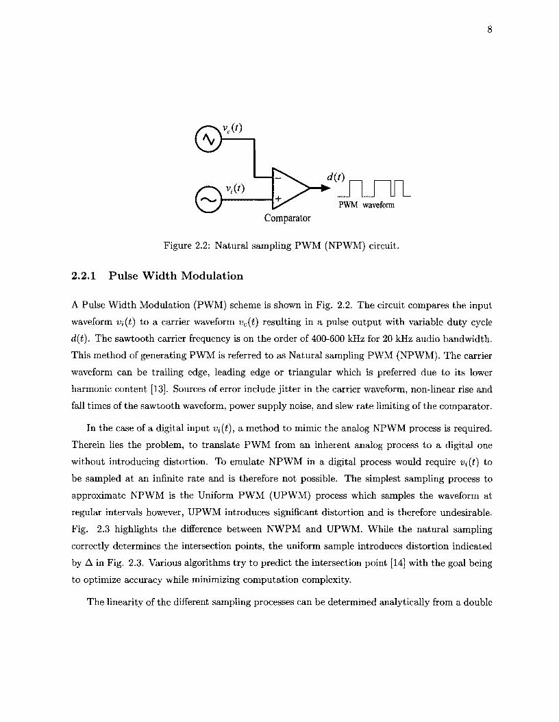
2.2.1 P u lse W id th M od u lation
A Pulse W idth Modulation (PWM) scheme is shown in Fig. 2.2. The circuit compares the input
waveform Vi(t) to a carrier waveform vc(t) resulting in a pulse output with variable duty cycle
d(t). The sawtooth carrier frequency is on the order of 400-600 kHz for 20 kHz audio bandwidth.
This method of generating PWM is referred to as Natural sampling PWM (NPWM). The carrier
waveform can be trailing edge, leading edge or triangular which is preferred due to its lower
harmonic content [13]. Sources of error include jitte r in the carrier waveform, non-linear rise and
fall times of the sawtooth waveform, power supply noise, and slew rate limiting of the comparator.
In the case of a digital input u,(f), a method to mimic the analog NPWM process is required.
Therein lies the problem, to translate PW M from an inherent analog process to a digital one
without introducing distortion. To emulate NPW M in a digital process would require Vi(t) to
be sampled a t an infinite rate and is therefore not possible. The simplest sampling process to
approximate NPW M is the Uniform PW M (UPWM) process which samples the waveform at
regular intervals however, UPWM introduces significant distortion and is therefore undesirable.
Fig. 2.3 highlights the difference between NWPM and UPWM. While the natural sampling
correctly determines the intersection points, the uniform sample introduces distortion indicated
by A in Fig. 2.3. Various algorithms try to predict the intersection point [14] with the goal being
to optimize accuracy while minimizing computation complexity.
The linearity of the different sampling processes can be determined analytically from a double

9
v,(0
NPWM
2T
UPWM
dT , 2 T,0 S
Figure 2.3: PW M waveforms for the natural sampling (NPWM) and uniform sampling (UPWM) processes.

10
fourier series expansion [14]. The final results of which are given in equations (2.2.1) and (2.2.2)
for NPWM and UPWM respectively. These equations are useful in calculating the distortion
arising from a particular sampling process.
MF n p w m {£) = K + — cos (uJit) + y
m= 1 oo ’ ±oo
rmr m nsin (mu)ct — 2rmrk)
m = 1 n = ± lm n
E x—\ Jn(m nM ) ( nny ------- sin ( m u ct + n u it — 2m nk ) (2-2.1)
OO T | TlTTOJi |rp V 2nnkui nnFupWM{t) = K - > — — — sin nuJit-------------------—
n = l \ 2
°° sin(mu;ci) — Jo(m7rM) sin(mujct — 2mnk)
m= 1^ ^ Jn((muJc + n w i ) ^ - ) .> / ----- ?------------ sm
' *-? (mujc + nu!i)m = l n = ± 1 v '
m n
{mojc + nuii) ( t —2nkUJa
nn~2
(2 .2 .2)
For the NPWM process the four components of (2.2.1) are explained as follows,
• The first term K is simply the DC component.
• The second term represents the input signal from which we note there are no harmonics, only the fundamental
• The third term represents the high frequency carrier and its harmonics. Since the carrier frequency is much higher than the input signal it is outside the audio band. These tones are usually low pass filtered.
• The fourth term is the intermodulation products of the carrier and input signal. It is noted tha t for n = -l to -oo foldback distortion occurs. The degree of distortion is a function of the modulation index M, the ratio of cvc/^ i and the bandwidth of interest.
For UPWM the first, third and fourth terms in (2.2.2) are similar to (2.2.1). The second term
corresponds to the input signal and its harmonics which are distortion terms absent in NPWM.
Fig. 2.4 is a plot of the UPWM second and third order harmonics normalized to the fundamental
for a modulation index M = l. For the UPWM process it is evident that a large oversampling
ratio is required for low harmonic distortion. For example, a 20 kHz bandwidth signal with a
sampling ratio on the order of 5,000 (100MHz) would generate -70dBc second order distortion.
A PW M waveform could be directly derived from the digital data using the circuit shown in

11
UPWM Harmonic Distortion
— Second order- Third order
-20
-40
3 -50aE<
-70
-80
-90
-100
O S R ( a> /to .)
Figure 2.4: Second and third order harmonic distortion relative to fundamental with M = l.
Fig. 2.5. This circuit converts a b-bit input at sample rate fs to a PW M waveform with the same
frequency as fs. Note th a t the counter requires a high speed 2bfs clock to define the timing edges
for the digital modulator and is therefore critical in maintaining system performance and limits
the practical application of this architecture. For PCM audio system with 16-bit resolution and
a samples rate of 44.1 kHz the minimum pulse width tha t must be precisely controlled is,
6t — -^-T- = — ^ = 346 ps (2.2.3)2bf s 216 • 44.1 x 10³ v '
which is on the order of 2.9 GHz. While this is possible with modern CMOS processes several
complications arise. Three predominant limitations towards a practical implementation are,
• The high speed bit clock must be stable so as not introduce jitter. Any jitte r in the clock signal creates distortion which degrades audio quality. The jitte r must be limited to a small fraction of the minimum pulse width.
• The digital circuit must eventually drive the switching amplifier. A Class D switching amplifier is a large inverter (with large parasitics) capable of driving low impedance loads. To drive the switching amplifier with fast slew rates will require a large tapering ratio. This would increase current consumption and reduce overall efficiency.
• The direct implementation of PCM to PW M in this manner is a uniform sampling process

12
Sample Clock : f s
Parallel inputload data
Counter/ „ , Outl
com parator
CLK
sR SR Latch 0ut2
CLK
f = *0012(b-bits)
::::z ■ n
Bit Clock : 2 b xfs
Out2
Figure 2.5: Direct digital conversion PCM to PWM
(UPWM) and is inherently non-linear. To improve linearity the data must be oversampled which in turn further compounds the jitte r and power issues.
In conclusion, the direct PCM to PWM digital conversion is not practical. As such there are
a variety of methods to reduce harmonic distortion in the PCM to PWM process [14], [15], [16].
2 .2 .2 S igm a-D elta M od u lation
Sigma-Delta (SA or SDM) modulators are used extensively in data converter applications. Tra
ditional Nyquist rate converters operate moderately above the Nyquist rate (twice the signal
bandwidth) and their linearity and accuracy are inherently limited by component matching ac
curacy. On the other hand SDM converters operate on the principle of oversampling and noise
shaping which requires considerable digital circuitry and some analog stages. While such con
verters tend to operate at significantly higher sampling rates compared to Nyquist converters, the
stringent component matching accuracy requirements are relaxed. Thus, SDM data converters
obtain higher resolution a t the expense of increased digital circuitry and higher frequencies. As
CMOS devices continue to scale smaller the trade-off becomes more economical and oversampling
converters will continue to infringe on applications once dominated by Nyquist converters. Audio
applications with bandwidths of 20kHz and high resolution requirements on the order of 16-24

13
E E(z)
u(z) : '■ V1
iY(z) V(z) .
□ p rz - 1 • • • •
(a) First order Sigma-Delta Modulator
PSD Signal
NoiseShaping
f.s
(b) Time-domain waveforms (c) Output power spectral density
Figure 2.6: First order Sigma-Delta modulator: a) System block diagram, b) Input and output time domain waveforms, c) Noise shaped spectral output.
bits are ideally suited to SDM implementation.
The operation of a first order modulator is illustrated in Fig. 2.6 with input U(z), output V(z)
and quantization error E(z). In the case of an ADC the quantization error E(z) models the differ
ence between the discrete ADC levels and the analog input signal. Detailed and comprehensive
analysis can be found in [17]. Linear analysis of Fig. 2.6a yields,
V(z) = z~ l U(z) + (1 - z~ l )E{z) (2.2.4)
which indicates tha t the output is the sum of the delayed input U(z) plus E(z) multiplied by
(1 — z " 1) which has a high pass transfer function as shown in Fig. 2.6c. This characteristic of
suppressing baseband noise and shifting it to higher frequencies is referred to as noise shaping.
Higher Lth order loop filters yield more aggressive noise shaping (1—z -1 )L which in turn, increases
the resolution by L + l/2 bits. Fig. 2.6b is a time domain plot of the modulated output for a
sinusoidal input.
14
2.3 D igital to Analog Converter
An ideal Digital to Analog Converter (DAC) converts the digital input into an analog signal
without distortion and a high Signal to Noise Ratio (SNR). The DAC can be either of Nyquist or
over sampled architecture. In the Nyquist case the modulator block in Fig. 2.1 is not necessary.
The Nyquist DAC directly converts the 16b output from the digital audio source to an equivalent
analog signal.
W ith an oversampling DAC a modulator is used to reduce the number of bits. For example,
a SDM can effectively reduced the 16b to a single bit with high fidelity. In this case the binary
output is is directly compatible with switching mode amplifiers.
2.4 Power Amplifier
The Power Amplifier (PA) must reliably and efficiently deliver sufficient power to the load. In
this application the load is a headphone typically with an impedance of 16fl or 32T1. PA designs
with low efficiency will generate heat, dissipate significant power and increase battery drain.
Power amplifiers are generally classified into two categories either linear or switching. The
term “linear” does not imply tha t such amplifiers do not exhibit any non-linear behavior but
rather act as a current source with the output voltage proportional to the input. T hat is, the
transistor is in the saturation region for some period of time. Examples of linear PA’s are Class
A, AB, B and C.
In switching mode PA’s such as Class D, E and S, the transistor operates as a switch in either
an open or short state. These PA’s are directly compatible with pulse modulation schemes such
as PWM or SDM being the most common.
2.4 .1 Linear A m plifiers
A schematic for the linear amplifiers Class A, AB, B and C is shown in Fig. 2.7 where M l is
nMOS transistor, RFC is a choke, Cb is DC blocking capacitor, LC is a parallel tank circuit and
R is the load resistor. The tank circuit is resonant at the operating frequency a t which point it
is ideally infinite impedance and a short circuit for all other frequencies. This ensures tha t the
output voltage across the load resistor is sinusoidal. Depending on the bias conditions imposed
at vg the current conduction i<j in the driver transistor will vary. The fraction of a full cycle for

15
RFC
Ml
Figure 2.7: Basic circuit configuration of a single ended Class A, AB, B or C amplifier.
Table 2.1: Conduction angles and efficiency ratings for linear mode amplifiers.Class Conduction Angle Maximum Theoretical Efficiency
A 360° 50%AB 180° - 360° 50% - 78.5%B
OO00t—H 78.5%C
Oo
00 T—H1Oo
78.5% - 100%
which id flows is referred to as the conduction angle where a full cycle is 360°.
Table 2.1 lists the different classes of linear amplifiers according to the conduction angles from
360° for full conduction to 0° for no conduction. In addition, the maximum theoretical efficiency
corresponding to each class is specified.
The efficiency values in Table 2.1 are the theoretical limit under maximum output power
conditions. When the output voltage is less than full scale the efficiency is significantly reduced.
In this case, the difference between the output and the supply voltage is dropped across the
output transistor resulting in wasted energy. There are many variations of the linear amplifier
design which attem pt to alleviate this affect.
As an example, one architecture to minimize this affect is the Class G amplifier in which
multiple supply voltages are used [18], [1]. G2 refers to two voltage supplies, G3 to three supplies
and so on. By lowering the supply voltage for low level signals the energy wasted in the output
transistor is reduced. While improving the overall efficiency the requirement for multiple supply

16
Increasing Power dissipation
Class A
Class AB
Class D
Figure 2.8: Current-Voltage plane operating locus of different power amplifier classes,
voltages, drive control circuitry and crossover distortion detract from the efficiency improvements.
2.4 .2 Sw itch ing M o d e Pow er A m plifiers
Switching Mode Power Amplifiers (SMPA) operate fundamentally differently than linear ampli
fiers. Fig. 2.8 illustrates the typical load lines in the current-voltage plane for different classes of
amplifiers and illustrates the difference between linear and switching amplifiers. For SMPAs in
which the devices are either switched off (no current flow) or on (current flow with ideally zero on
resistance) the amplifier dissipates no power. Conventional Class A, AB and C designs have load
lines tha t swing through a locus with a high current-voltage (power) product while the switching
amplifier essentially hugs the axis with small current-voltage product, ideally zero. Furthermore,
it will be shown tha t Class A through C amplifiers theoretical efficiency is reduced as the drive
level is reduced relative to full scale while SMPAs are essentially constant. This is im portant
in audio systems as the volume is often backed off from full scale in typical background music
listening.
An inherent disadvantage of SMPAs is Electromagnetic Interference (EMI) arising from the
transient rail-to-rail switching action. EMI can result in failure to meet regulated FCC (North
America) or CE (European) standards. The EMI frequency spectrum is modulation dependant

17
and as such is different for PWM and SDM implementations. EMI can cause conductive or
radiated interference.
SMPAs are identified using an alphabetic nomenclature in continuation from the linear am
plifiers. The most common switching amplifiers are Class D and E. The difference being related
to the application requirements on bandwidth and switching frequency. Class D is applicable at
lower frequencies (up to MHz range) and Class E is adopted at higher frequencies (up to GHz
range). For applications with switching frequencies on the order of kHz to the MHz range the
switching time (rise and fall times) are not a significant fraction of the switching period. In these
cases Class D is suitable. Such applications include DC-DC converters and audio amplifiers for
example. For audio applications with PWM or SDM signals the switching rate may be a few
hundred kHz to a few MHz depending on the m odulator architecture.
Audio applications of Class D have been commercially adopted by many semiconductor com
panies. The designs vary in output power capability depending on intended use, i.e. low power
portable designs (mW output) or high power home or automotive (several watts) audio systems.
Some example manufacturer part numbers and output power capabilities are Texas Instruments
(TPA2010D1 / 2.5W), Maxim (MAX9700 / 1.2W, MAX9709 / 50W) and Wolfson (WM88956 /
40mW).
Applications at high frequency can be limited by the ability of the transistor to behave as
a near ideal switch. At Radio Frequencies (RF) the switching time can become a significant
fraction of the switching period thereby reducing efficiency while increasing noise and distortion.
In an attem pt to overcome finite switching times the Class E amplifier was developed [19]. Class
E is a switching mode amplifier which has a load network synthesized to eliminate simultaneous
voltage and current during switching and is tolerant to finite switching times.
The standard binary SMPA switching scheme can be extended to multi-levels. This reduces
the peak voltage across each device and minimizes switching losses by lowering the switching
frequency [2 0 ].
2.5 Speakers
Speakers are transducers which convert electrical signals into audible sound waves. They are
specified by bandwidth, impedance, sensitivity and maximum power capability. For example, a
low cost pair of ear bud type headphone speakers (Sony MDR-E8181) have a 16 ff impedance, 12

18
Headphone impedance800 100
MagnitudePhase
600
2 400
-50200
16ft
-100
Frequency (Hz)
Figure 2.9: Headphone impedance measurement of Sony MDR-E8181.
Hz to 22 kHz bandwidth and a 108 dB /m W sensitivity. The impedance measurement is shown
in Fig. 2.9. The impedance is 16 fi over the audio bandwidth and exhibits a resonance at 2.25
MHz.
A Class D switching mode amplifier with single and differential load configurations is shown
in Fig. 2.10. Headphones are typically connected in the single ended configuration while earpiece
or hands free speakers are connected in a differential or Bridge Tied Load (BTL) configuration.
BTL offers the advantage of suppressing common mode noise and providing twice the voltage
swing across the load for a given supply voltage. This provides a quadrature increase in available
power. The disadvantage of BTL is the need for extra components.
a) Single ended b) Differential BTL
Figure 2.10: Speaker connection configurations, a) single ended, b) differential or BTL.

19
2.6 Power Amplifier Efficiency
In this section PA efficiency is analyzed for both linear and switching mode amplifiers. Efficiency
formulas are defined followed by theoretical calculations for both linear and switching mode
amplifiers.
2.6 .1 D efin ition s
Efficiency is broadly defined as the ratio of the output power to the input power. In specifying the
efficiency one must specify whether or not the input power includes both the DC supply and the
RF drive power or only the DC supply power. The most common definitions are as follows [21].
The collector efficiency is defined as,
( 2 ' 6 1 )
Where P0 is the output power dissipated in the load and Pdc = VdcJdc is the power extracted
from the DC supply to the collector or drain of the power amplifier. The Pa term includes the
fundamental and harmonic components but the harmonics tend to be negligible relative to the
fundamental.
The overall efficiency takes into account the input drive level which can be significant and is
defined as,
7)0 = Pdc + P in = P dc + P o / G p ( 2 ' 6 ‘2 )
where the power gain is given as,
G P = (2.6.3)in
Finally, the power added efficiency which takes into account the input power is defined as,
_ P q - P in P> ~ P o /G p
^ " P * P * 1 '
From the various definitions it is apparent tha t one must use caution to compare different

20
Maximum T heoretical Efficiency
0.95
0.9
C lass B0.85
C lass AB
w 0.75E3E
0.7 -2
0.65
0.6
Class A0.55
0.5120 200
C onduction angle (deg)160
Conduction240 280 320 360
Figure 2.11: Maximum theoretical collector efficiency r\c versus conduction angle.
designs using the same criteria and efficiency formulas. The standard within this report will be
to use the collector efficiency definition.
2.6 .2 Linear Pow er A m plifier E fficiency
Fig. 2.11 is an extension of Table 2.1 in which the efficiency is plotted for all conduction angles.
We observe tha t theoretically 100% efficiency can be achieved, however as indicated in Fig. 2.12,
the output power decreases to zero. This implies th a t as we decrease the conduction angle to
increase efficiency we must increase the peak collector current to satisfy the drive requirements.
Ultimately, the selection of the conduction angle is a trade-off among collector efficiency, peak
collector current and power gain. Detailed derivations of the equations to create these plots can
be found in [2 1 ] and [2 2 ].
It should be emphasized tha t the efficiencies of Fig. 2.11 are for an ideal circuit with full scale
output. Should the output power be reduced so will the efficiency. To examine the impact on
efficiency due to output swing we define,

21
e
I13
0.6uoz
i 04'5»s
0.2
40 120 160Conduction
200Conduction angle (deg)
240 280 320 360
Figure 2.12: Normalized maximum power output capability versus conduction angle.
p Vcc(2.6.5)
where Vop is the peak amplitude of the sinusoidal output as measured at the load resistor (0 <
/3 < 1). The collector efficiency equations which take into account drive levels for Class-A, B and
G (two levels) amplifiers are,
VA 2(2 .6 .6)
where
VB = 07r4
/?f(a + (1 — a ) cos#t)
(2.6.7)
(2 .6 .8)
e t =7r/2 : fi < a
arcsin(a//3) : ft > a
and a is the fraction of Vcc for the two level Class G amplifier.

22
0.9
0.8
0.7
S 0.5
Class G2 o«1/20.4
0.3
0.2Class A
-40 -35 -30 -20Output level p (dBFS)
-15 -1 0
Figure 2.13: Collector efficiency t]c of ideal Class-A, B, G2 (a —0.5) amplifiers.
The collector efficiency for Class A, B and G are plotted in Fig. 2.13 with f3 expressed in
dB full scale (/3=1 is 0 dBfs). Significant efficiency reduction is encountered as (3 decreases.
Furthermore, real world signals with amplitude variation will effectively reduce the efficiency.
The peak to average or crest factor for a waveform 7 can be calculated by,
C F = hlpeak (2 .6 .9 )Irms
which for a sinusoid is \/2 or 3dB. The net impact of the crest factor is to reduce the average
efficiency of the amplifier. Music and audio typically are modeled with Gaussian probability
distribution functions from which the average efficiency is calculated. The average efficiency for
various crest factors with optimized a param eter at each crest factor is plotted in Fig. 2.14.
Given the efficiency dependance on output power (volume), it would be useful to know pre
ferred listener volume settings. An empirical study [23] indicates tha t for 99% of time the listener
will set the music volume at or below -24 dBfs. While this is a generalization, it serves to high
light tha t many listeners tend to set the volume well below full scale. For the linear amplifier
designs this is detrimental to efficiency however, Class D amplifiers maintain a theoretical 100%
efficiency.
By way of example consider what a Class B amplifier might realistically achieve in terms of
23
0.9
Class G30.7
0.6-Class G2
0.5
Class B& 0.4
0.3
0.2
Crest Factor (dB)
Figure 2.14: Average efficiency for Class B, G2 (two level) and G3 (three level) for audio signals with Gaussian probability distribution function [1].
efficiency. The efficiency will be very low considering a typical audio signal has a crest factor on
the order of 12-20 dB and the listener will generally back off the volume anywhere from -10 to -40
dBfs. Assuming a modest crest factor of lOdB from Fig. 2.14 we obtain r/avg « 39%. Furthermore,
the efficiency must be derated according to the volume setting. Assuming the volume is set at
-20 dBfs from (2.6.7) rjavg ss 3.9%. The efficiency is significantly lower then the theoretical limit
of 78.5%.
To estimate the efficiency the following factors need to be considered,
• Consider which Class of PA is to be used. e.g. A, B, AB, G2, G3, etc.
• Estimate the crest factor and extrapolate r)avg from Fig. 2.14.
• Estimate the nominal volume setting (dBFS).
• Derate the efficiency according to the corresponding formula for the class of PA being used.
• Factor in any non-idealities of the circuit such as component losses and nominal bias.
2 .6 .3 C lass-D E fficiency
As previously stated, classical amplifier designs such as Class A and AB suffer from poor efficiency
at low drive levels. For signals with high crest factors the overall efficiency can be very poor.

Figure 2.15: Class D circuit: (a) MOS circuit schematic, (b) equivalent ideal circuit.
These amplifiers provide the best efficiency results with constant envelope modulation schemes
and high drive levels. Alternatively, the theoretical efficiency of Class D amplifiers is 100%
independent of output level.
Class D is a switching mode amplifier using two active devices driven in a two-pole switch
configuration. The output of which defines a rectangular voltage waveform at the input to a tuned
load circuit. The load circuit uses either a band-pass or low-pass filter to remove harmonics and
extract the fundamental. For audio systems a low pass filter is required. A Class D amplifier
with a series tuned LC filter and its switching equivalent is shown in Fig. 2.15a. The equivalent
ideal switching model in Fig. 2.15b. In analyzing the circuit the following assumptions are made:
• The series resonant LC circuit is tuned to the switching frequency at which point it exhibits zero impedance. At all other frequencies the impedance is infinite. This ensures a sinusoidal output at the switching frequency and eliminates the inherent harmonics from the square wave voltage waveform imposed by the switching action at the input to the load network.
• The MOS switches have zero ON resistance and infinite OFF resistance and can switch instantaneously without crossover distortion.
• Device parasitics are ignored and the load network components are ideal.
Assuming a 50% duty cycle square wave input, the voltage waveform of Fig. 2-16a can be
expressed mathematically as,
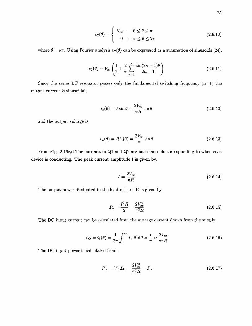
25
- , , Vcc ■ o < 9 < 7Tv2(0) = { - - (2 .6 .1 0 )
0 : 7T < 6 < 2 tt
where 6 = u t. Using Fourier analysis V2 (0) can be expressed as a summation of sinusoids [24],
<n\ t r ( 1 2 ^ sin(2 n — 1) # \^ ) = v ^ ( - + - g ^n _ 1 , j (2 .6 .1 1 )
Since the series LC resonator passes only the fundamental switching frequency (n = l) the
output current is sinusoidal,
2Vio{0) = I sin6 = —^ s i n 0 (2 .6 .1 2 )
7T xt
and the output voltage is,
2 Uvo(0) = R io(0) = — — sin# (2.6.13)
7T
From Fig. 2.16c,d The currents in Q l and Q2 are half sinusoids corresponding to when each
device is conducting. The peak current amplitude I is given by,
21// = —f (2.6.14)
ttR
The output power dissipated in the load resistor R is given by,
I 2R 2V 2P „ = — (2. 6. 15)
The DC input current can be calculated from the average current drawn from the supply,
i r2* t 21/' * - < . < » ) - S j [ = ^ (2-6.16)
The DC input power is calculated from,
Pdc = VdcIdc = ^ = Po (2.6.17)
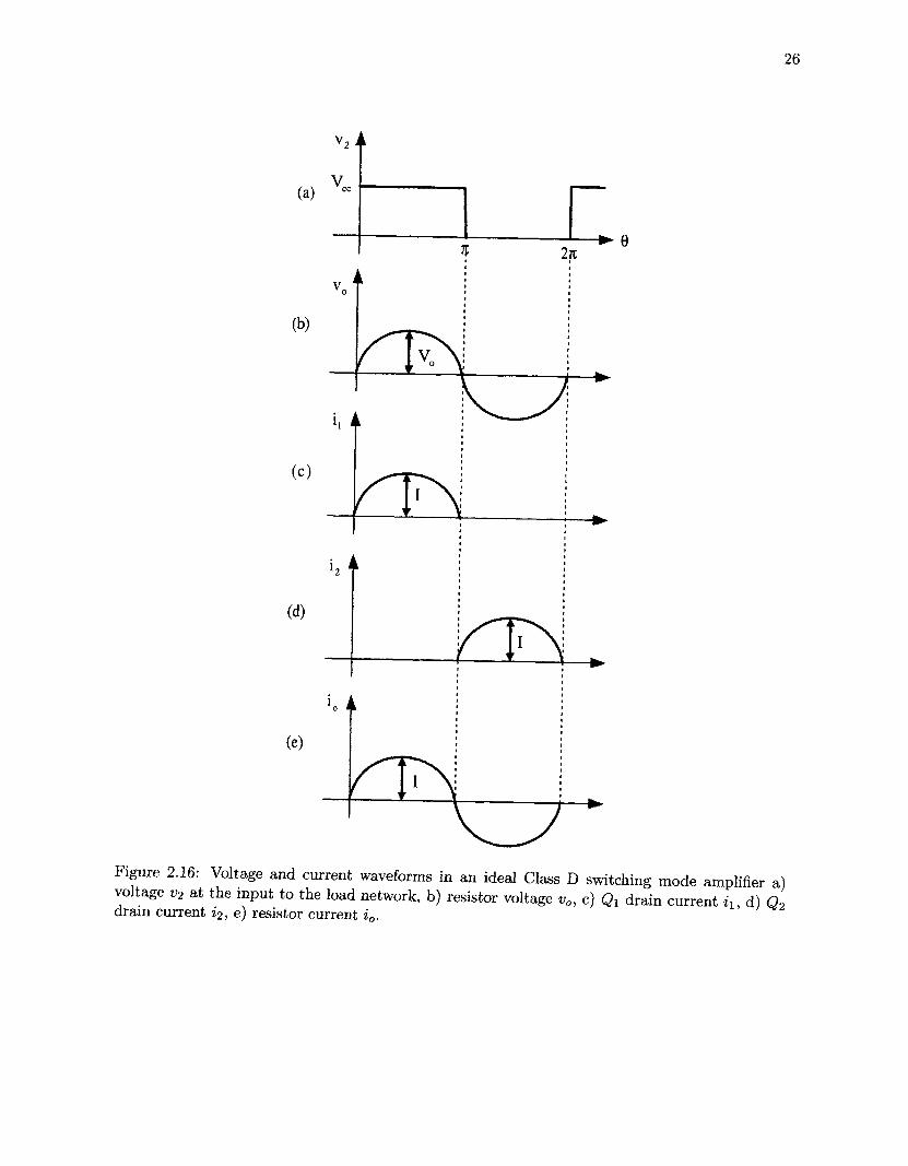
26
(a)
► 9
(b)
*►
(c)
(d)
(e)
Figure 2.16: Voltage and current waveforms in an ideal Class D switching mode amplifier a) voltage t>2 a t the input to the load network, b) resistor voltage v0, c) Q\ drain current u , d) Q 2
drain current 22, e) resistor current iQ.
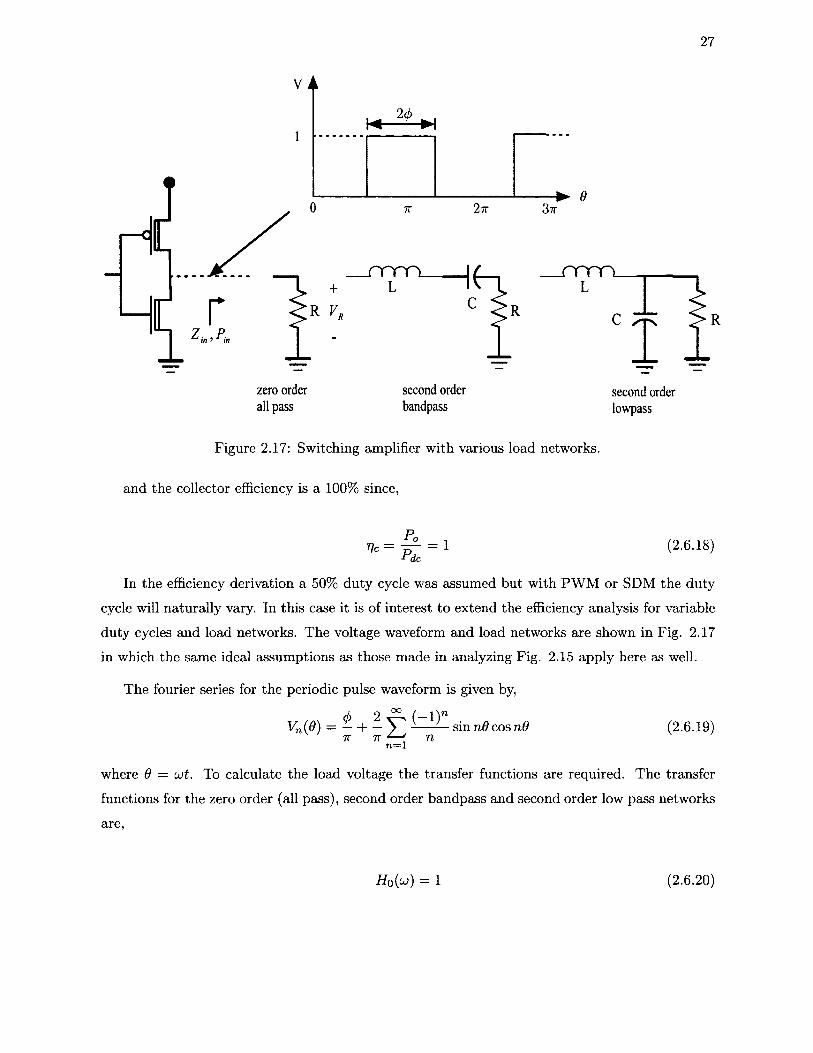
27
V i k
c
m m
R
zero order all pass
second order bandpass
second order lowpass
Figure 2.17: Switching amplifier with various load networks,
and the collector efficiency is a 1 0 0 % since,
Pdc1 (2.6.18)
In the efficiency derivation a 50% duty cycle was assumed but with PW M or SDM the duty
cycle will naturally vary. In this case it is of interest to extend the efficiency analysis for variable
duty cycles and load networks. The voltage waveform and load networks are shown in Fig. 2.17
in which the same ideal assumptions as those made in analyzing Fig. 2.15 apply here as well.
The fourier series for the periodic pulse waveform is given by,
d> 2 -°° , ( — l l n Vn{6) = — I— sin n6 cos n9
7T 7T ‘ ^n = l
7T IT n(2.6.19)
where 6 = cot. To calculate the load voltage the transfer functions are required. The transfer
functions for the zero order (all pass), second order bandpass and second order low pass networks
are,
( 2 .6 .20 )

28
HbP(w) R + . ^ L _ 1/a;C) (2.6.21)
Hzp(w) = 1 - t f L C + j u L / R (2’6'22)
The load networks are passive and linear therefore superposition can be used to calculate the
output voltage. For the fundamental (n = l) and harmonic components ( n>l ) output voltage
across the load resistor R is given by,
VR(n) = H Vn (2.6.23)
from which the output power can be calculated
p R(n) = (2-6.24)
The input power can be calculated from the voltage and current waveforms,
° ° y j ° ° ^ t / 2
P™ COSiP = Y l 9 COS (2.6.25)n = l n = l
where <p is the input voltage and current phase difference and Z{n is the network input impedance.
The efficiency can then be calculated by taking the ratio of the fundamental output power to the
total input power,
r i = p^ ) (2.6.26)•*1in
As an quantitative example assume a switching frequency of 1 MHz, R=16 L=1 mH, and
C=25.3 nF for the circuit in Fig. 2.17. Using these component values the efficiency is calculated
according to (2.6.26) and plotted in Fig. 2.18. Based on the results the following observations
are made:
• Even with ideal switching the zero order network does not result in 100% efficiency. This is due to energy wasted in the form of harmonics. The peak efficiency for the zero order model of 81% occurs at <f> = 90°.
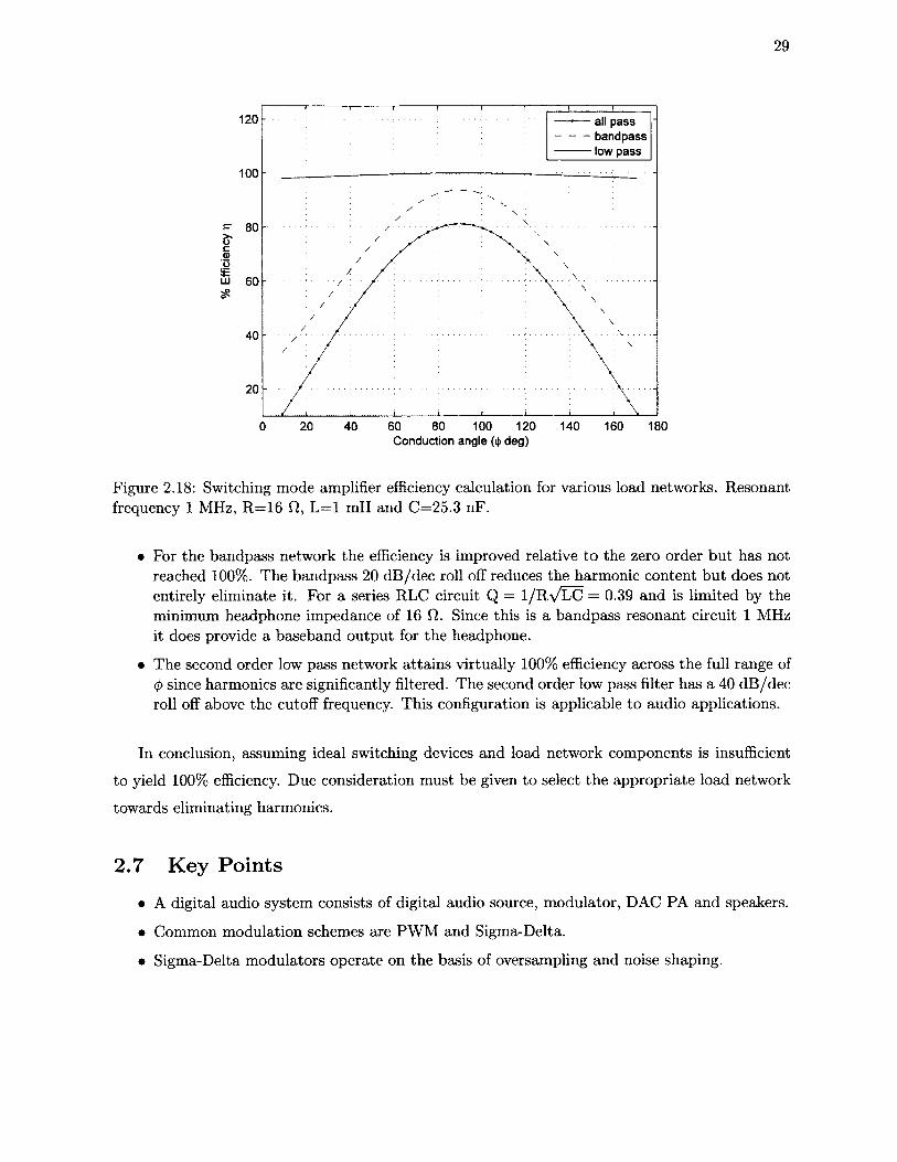
29
120 all pass bandpass low pass
100
0 20 60 80 100 120 140 160 18040Conduction angle (0 deg)
Figure 2.18: Switching mode amplifier efficiency calculation for various load networks. Resonant frequency 1 MHz, R=16 Cl, L=1 mH and C=25.3 nF.
• For the bandpass network the efficiency is improved relative to the zero order but has not reached 100%. The bandpass 20 dB/dec roll off reduces the harmonic content but does not entirely eliminate it. For a series RLC circuit Q = 1 /R \/L C = 0.39 and is limited by the minimum headphone impedance of 16 Cl. Since this is a bandpass resonant circuit 1 MHz it does provide a baseband output for the headphone.
• The second order low pass network attains virtually 100% efficiency across the full range of 4> since harmonics are significantly filtered. The second order low pass filter has a 40 dB/dec roll off above the cutoff frequency. This configuration is applicable to audio applications.
In conclusion, assuming ideal switching devices and load network components is insufficient
to yield 100% efficiency. Due consideration must be given to select the appropriate load network
towards eliminating harmonics.
2.7 K ey Points
• A digital audio system consists of digital audio source, modulator, DAC PA and speakers.
• Common modulation schemes are PWM and Sigma-Delta.
• Sigma-Delta modulators operate on the basis of oversampling and noise shaping.

30
• The analog version of PW M is referred to as natural sampling or NWPM. It does not distort the input signal.
• A discrete time PW M process with unform sampling UPWM distorts the input signal.
• The two classes of PA’s are linear and switching mode.
• Linear amplifiers achieve maximum efficiency a t full scale output. The efficiency is reduced below full scale.
• Ideal switching mode amplifiers can achieve 100% efficiency a t or below full scale output. This assume th a t the devices behave as ideal swithches and an appropriate low pass filter network is present to remove harmonics.
• The collector efficiency is defined as r]c = P0/Pdc where Pa is the output power delivered to the load and Pcic = VdcIdc is the power from the supply.

Chapter 3
Audio Amplifier Technology R eview
This chapter begins by providing a table of system specifications for low power stereo headphone
applications. This is followed by a discussion on typical sources of amplifier distortion and
various correction techniques. A literature review of switching mode amplifier designs with various
modulation and linearization techniques are briefly explained.
The majority of the papers are targeted towards full 20kHz bandwidth stereo applications
and a few towards hearing aids with reduced bandwidth requirements. Many switching mode
PA designs assume analog inputs and therefore require a DAC to interface with the digital audio
source. For battery operated devices the goal is to merge the DAC and PA in a single chip
scalable solution for rapid deployment in new fabrication processes.
3.1 System Specifications
The target specifications for a low power portable digital audio system are summarized in Table
3.1. The nominal supply voltage is based on a 130 nm CMOS process and will change depending
on the chosen CMOS technology. At the nominal audio output power of 0.1 mW the system power
consumption should be 10 mW or less for two channel operation. The total power consumption
was selected to be competitive with commercial parts (low-voltage and low-power stereo audio
digital-to-analog converter with headphone amplifier TI PCM1770).
The headphone sensitivity and output power are chosen to produce an output level of 100
dB. For a 5 mW output and a 95 dB /m W sensitive headphone the audio output will be 102 and
105 dB for a 32 D and 16 fi headphones respectively. The output power should vary less than 1
dB over the audio band.
31

32
Table 3.1: Low power digital audio system specifications.
Parameter Conditions ValuesSupply Voltage Max 1.2 VNominal output power 16 or 32 O 0.1 mWPower consumption Nominal output power, stereo 10 mWMax output power 16 Q 10 mWHeadphone sensitivity min 95 dB /m WLoad Impedance min / max 16 / 32 QFrequency response 20 Hz to 20 kHz < ±0.5 dBTotal Harmonic Distortion 1 kHz -70 dBcSNR A-weighted @ o dBm >90dBPower supply rejection <20 kHz >40dB
The Total Harmonic Distortion (THD) is a figure of merit calculated by taking the ratio of
the harmonic distortion relative to the fundamental. This can be expressed as a percentage,
THD = x 100%. (3.1.1)i=2
For good quality audio performance a THD on the order of 0.01 to 0.1% (-80 to -20dB) is required.
For this application the target is 0.03% or -70dB. To account for noise and distortion the THD+N
is often specified and can be calculated as followzs
/ V ° ° V-2 4- AT \THD+N = 10 log 1=2 y 2 ° J (3.1.2)
where N a is the noise power integrated over the bandwidth of interest.
The frequency response of human hearing is inherently non-linear across the audio band.
Various weighting filters, using the nomenclature A, B, C and D, have been developed to model
this phenomena. Fig. 3.1 is a plot of the A-weighting filter model of human hearing sensitivity.
This filter is the most common model applied in stereo applications. Tones in the 1 - 6 kHz range
are accentuated and rapidly desensitized outside of this bandwidth. Signal to Noise Ratio (SNR)
measurements are often specified with the amplifier output filtered using A-weighting.
The Power Supply Rejection Ratio (PSRR) is an im portant parameter in order to maintain
quality audio performance. The systems ability to reject noise superimposed on the DC supply

33
A-weighted Fitter Response10
0
-1 0
-20
-40
-50
-60
-70
-8010 10k100 1k
Frequency (Hz)100k
Figure 3.1: A-Weighted filter response commonly used in audio measurements.
is determined by external power supply filtering, closed loop system response and deployment
of differential circuits on-chip. The supply noise is usually a small percentage of the DC value
so a 40dB target is a conservative specification to not not degrade the SNR. If good on-chip
PSRR is obtained this can reduce the complexity and cost of the external power supply filter.
In certain instances, such as in GSM handsets, a PSRR on the order of 65-80dB is required for
a direct battery connection. Otherwise, a linear regulator would be required to isolate the audio
system from the battery noise. This is obviously undesirable as the regulator will increase design
complexity and increase power consumption.
3.2 Sources of D istortion
Distortion arises from amplitude and/or timing errors in the modulated pulse density waveform.
Such errors can occur in the switching stage of Class D amplifiers resulting in harmonic distortion.
Many designs incorporate feedback which serves to lower the output impedance, enhance noise
immunity and most importantly, to linearize the PA. While feedback has many benefits, the
tradeoff is increased system complexity and potential instability.
Audio systems can have either analog or digital input. W ith analog input, the feedback can
be a passive or active network to realize the required frequency domain transfer function. If the

34
system is of the digital input type then the feedback signal must be digitized with an ADC. The
resolution, speed and power consumption of the ADC are challenging and limiting factors.
There are several sources of distortion arising from the switching action of the PA. The sources
can be broadly categorized into pulse timing and amplitude errors [25]. The timing errors arise
from:
• Finite switch-on and switch-off delays.
• Blanking or deadtime delay’s to ensure tha t simultaneous conduction of the nfet and pfet devices does not occur and thereby momentarily short the supply to ground [26], [27].
• Finite rise and fall times of the output when changing states.
• Reference clock jitter.
Sources of amplitude errors:
• Finite and nonlinear R^s which can cause amplitude modulation.
• Substrate coupled noise.
• Power supply noise.
• Power supply droop.
3.3 Linearization Techniques
While efficiency concerns have been discussed in detail we now tu rn our attention to compen
sation or linearization techniques. A high degree of linearity is essential for high quality audio
where harmonic distortion will degrade the THD performance. In wireless applications linearity
requirements are stringent to avoid intermodulation products can interfere with adjacent chan
nels. Thus, in applications like these, distortion will degrade system performance and must be
mitigated.
Linearization techniques can either be applied in an open or closed loop manner. The feasi
bility of the selected approach will depend on the system bandwidth requirements and frequency
of operation. Common techniques include negative feedback, indirect feedback, pre-distortion,
and feed forward.

35
E(s)* Y(s)X(s) G(s)
H(s)
Figure 3.2: Closed loop control system.
3.3.1 N eg a tiv e Feedback
Negative feedback is a classic technique which has been in use for decades. The concept is to
feedback a sample of the output and subtract it from the input to generate an error signal. The
closed loop response is to minimize this error, ideally setting it to zero. A closed loop control
system with feedback is shown in Fig. 3.2. This could represent an op-amp with open loop gain
G(s) and negative feedback H(s) for example.
In the open loop case H(s)=0 and output of the open loop system is
y (s) = G ( s ) X ( s ) (3.3.1)
In the closed loop H(s) ^ 0 resulting in an error signal E(s). The closed transfer functions
are,
r ( s > = r ^ m x w (3A 2)
and for the error function,
E « = (3'3 '3)
Therefore, if |1 +GH(s) \ > 1 over the bandwidth of interest the error will be reduced accordingly.
The process represented by the transfer function G(s) is subject to disturbances from the
external environment, process mismatches, tem perature, etc. In an amplifier it could be subject
to external power supply noise, substrate noise or have a non-linear transfer function tha t results
in distortion. From ( 3.3.1) it is clear in an open loop system tha t all disturbances or noise sources

36
directly affect the output, however a closed loop senses the changes and reduces the error by a
factor determined by (3.3.3).
The system sensitivity is defined as the percentage change in system transfer function to the
percentage change of the process transfer function [28]. The system transfer function is defined
as,
T (s) = ^ (3.3.4)
where the sensitivity is defined as,
A G (s)/G (s)
which in the limiting case can be expressed as a derivative,
_ dT(s ) / T(s ) dG(s) /G{s )
Applying (3.3.6) to the open loop transfer function gives,
s = m m (3.3.5)
(3.3.6)
s ° = % ¥ = 1§ = 1 (3-3‘7)
and any error introduced in G(s) will appear a t the output. For the closed loop sensitivity,
d T G 1 G 1“ dG T ~ (1 + G H) 2 G/{{ 1 + GH) ~ 1 + GH
(3.3.8)
and assuming |1 + GH\ > 1 the system error sensitivity is therefore reduced. Likewise, consider
the system feedback sensitivity,
qT d T H -G HH d H T 1 + G H ( ’
and assuming \GH\ 3> 1, then S 7H —> 1. Any error in H(s) will directly impact the output
response. Thus, care must be taken in designing the feedback network so as not to degrade
system performance.
While closed loop PA systems enhance linearity and reject noise there is also the possibility of
instability. Closed loop operation usually requires the addition of a compensation or loop filter.
From (3.3.2) the loop will be unstable when

37
\GH\ = 1 and ZG H = -180°. (3.3.10)
As a result the condition for stability becomes
\GH\ < 1 at ZG H = -180°. (3.3.11)
Two common stability parameters are Gain Margin (GM) and Phase Margin (PM). The
phase margin (PM) is the amount by which the phase of GH(s) is greater than —180° at unity
gain \GH\ = 1. The gain margin (GM) is the factor by which the gain is less than unity when
Z G H = -180°.
In the analysis thus far, the feedback has been assumed to occur instantaneously without
delay. In reality, loop delay is inevitable and, in some cases, significantly degrade the PM. The
phase shift (rads) caused by a loop delay r seconds is,
d e = - u r (3.3.12)
where co is the frequency of interest. At this point it is worth highlighting the significance of
(3.3.12) pertaining to analog and mixed signal control systems.
In purely analog control circuits, transistors typically have delays on the order of picoseconds.
Such delays are not significant even at RF frequencies and it is assumed th a t r —> 0.
In mixed signal systems there is invariably a conversion process from the analog to digital
domain. This is accomplished by and ADC which can be modelled as a sample and hold circuit.
Consider the continuous time waveform Ui(t) sampled every T seconds as shown in Fig. 3.3. The
result is, tha t the average u0(t), lags ut{t) by T /2 , or in other words r = T /2 . While this can be
alleviated by reducing T, an increase in power consumption, particularly in the ADC will arise.
The delay associated with the sample and hold process is one of the most im portant factors in
digital control systems [29].
In summary, feedback is an effective and widely used method to linearize audio amplifiers.
The feedback desensitizes the amplifier to external noise sources and environmental conditions.
The cost to achieve such benefits are,
• Increased complexity and extra circuitry associated with the feedback network.

38
Ui(t)
Sample and hold
Tu0(t)
sample period T
Figure 3.3: Sample and hold delay.
• Loss of gain relative to open loop.
• W ith feedback there are stability concerns while open loop systems are typically stable.
3 .3 .2 A ltern ative L inearization T echniques
Alternatives to direct feedback include indirect feedback, pre-distortion and feed-forward tech
niques. These methods are often chosen in applications where the stability and bandwidth limi
tations of direct feedback are problematic, typically a t RF and microwave frequencies. These are
often sophisticated high power applications such as cellular base station transm itters as opposed
to the low power IC applications considered here.
Two indirect feedback methods are polar and Cartesian correction where the RF output is
down converted and compared with the baseband input. In polar correction both amplitude and
phase are detected and corrected. Cartesian correction is an extension of polar correction applied
to quadrature I and Q systems common in many communication systems.
Pre-distortion is an open loop compensation technique. While compensation is not as precise
as closed loop systems it does have advantages in tha t stability and bandwidth limitations are
eliminated. In pre-distortion, the known amplitude and phase non-linearities are applied to the
input signal to offset the PA non-linear characteristics. While this technique can be effective
it is difficult to compensate for a wide variety of parameters such as temperature and process
variations.
The final technique is feed-forward compensation which has the accuracy of a feedback system

39
without the associated bandwidth and stability concerns, however such high performance comes
at a cost. The feed-forward loop requires complex gain and phase tracking circuitry as well as an
additional power amplifier which reduces the overall efficiency [30].
3.4 Switching M ode Audio Amplifiers
A typical pulse modulation system for audio applications is shown in Fig. 3.4. The audio
source is a standard 16 bits/ch PCM at 44.1 kHz. The pulse modulator converts the bitstream
into a series of binary pulses. The two predominate modulation schemes are PW M and EA.
These pulse modulators enable implementation of a Switching Mode Power Amplifier (SMPA)
with theoretical 100% efficiency. The output signal is demodulated by way of a low pass filter
preceding the speaker. The feedback control provides error correction to reduce distortion and
noise. In some instances suitable performance is obtained without feedback, such open loop
designs are susceptible to significant performance degradation. The trade-off with closed loop
systems is better performance at the expense of extra circuitry and potential instability, however
if properly designed significant performance enhancement can be obtained.
Jinn1011101 ...
PA
Feedbackcontrol
LPF/DemodPulse
ModulatorDigital Audio
Source
Figure 3.4: Pulse modulation system with feedback.
Class-D amplifiers with a theoretical 100% efficiency have received much attention in the
literature. These amplifiers in combination with a EA or PWM modulator provide a direct
digital to analog audio system. Though conceptually simple to design many challenges arise.
Ideally, one would like to achieve low distortion, high dynamic range, high SNR, high efficiency
and stability while driving low impedance loads. This often requires feedback to linearize the PA.
A literature review of various Class D designs is presented in the following sections.
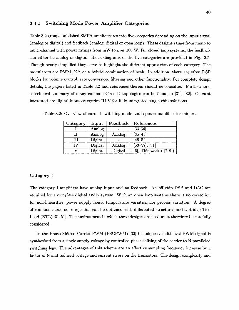
40
3.4 .1 S w itch in g M od e Pow er A m plifier C ategories
Table 3.2 groups published SMPA architectures into five categories depending on the input signal
(analog or digital) and feedback (analog, digital or open loop). These designs range from mono to
multi-channel with power ratings from mW to over 100 W. For closed loop systems, the feedback
can either be analog or digital. Block diagrams of the five categories are provided in Fig. 3.5.
Though overly simplified they serve to highlight the different approaches of each category. The
modulators are PWM, EA or a hybrid combination of both. In addition, there are often DSP
blocks for volume control, rate conversion, filtering and other functionality. For complete design
details, the papers listed in Table 3.2 and references therein should be consulted. Furthermore,
a technical summary of many common Class D topologies can be found in [31], [32]. Of most
interested are digital input categories III-V for fully integrated single chip solutions.
Table 3.2: Overview of current switching mode audio power amplifier techniques.
C a teg o ry In p u t F eedback R eferen cesI Analog - [33,34]II Analog Analog [35-45]III Digital - [46-52]IV Digital Analog [53-57], [31]V Digital Digital [6 ], This work ( [7,9])
C a te g o ry I
The category I amplifiers have analog input and no feedback. An off chip DSP and DAC are
required for a complete digital audio system. W ith an open loop systems there is no correction
for non-linearities, power supply noise, tem perature variation nor process variation. A degree
of common mode noise rejection can be obtained with differential structures and a Bridge Tied
Load (BTL) [31,51]. The environment in which these designs are used must therefore be carefully
considered.
In the Phase Shifted Carrier PWM (PSCPW M) [33] technique a multi-level PW M signal is
synthesized from a single supply voltage by controlled phase shifting of the carrier to N paralleled
switching legs. The advantages of this scheme are an effective sampling frequency increase by a
factor of N and reduced voltage and current stress on the transistors. The design complexity and
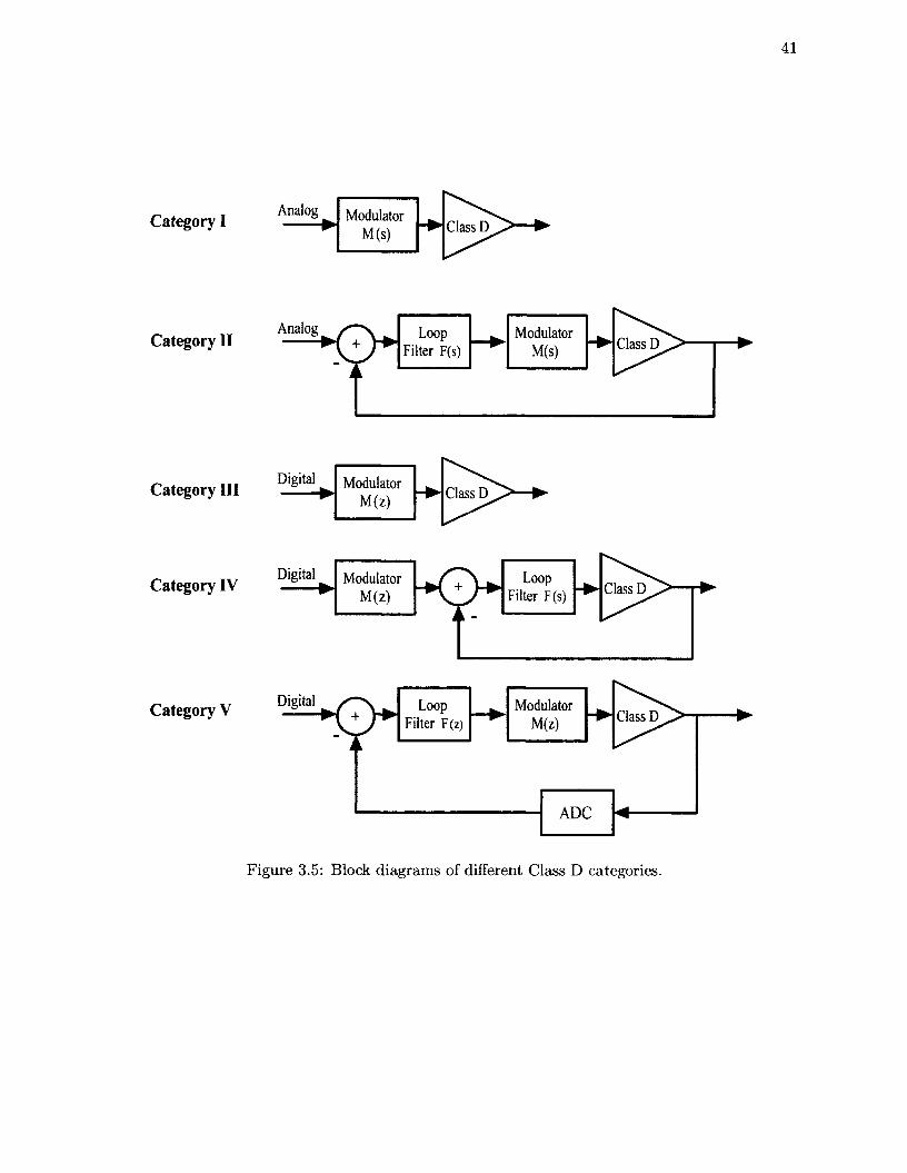
Category I
Category II
Category III
Category IV
Category V
41
Analog ModulatorM(s) Class D
Analog Loop Filter F(s)
ModulatorM(s) Class D
Digital ModulatorClass D
Digital Loop Filter F(s)
ModulatorM(z) Class D
Digital ModulatorM(z)
Loop Filter F(z) Class D
ADC
Figure 3.5: Block diagrams of different Class D categories.

42
cost will increase due to more switching legs, increased filtering components and phase shifting
circuitry sensitivity.
An fully integrated 0.25 pm CMOS design [34] implements a 3rd order single bit Sigma-Delta
modulator. To reduce conduction losses and achieve high efficiency, the switching stage must
have a much lower Rds than the load impedance. To accomplish this the switching transistors are
very large, Wp = 34,000 pm. The switching stage is driven by a series of six tapered inverters.
An efficiency of 91% at 1 W power into a 4 Q. load is achieved. While the efficiency is very high at
full output power the efficiency below full scale is not specified. Its possible the efficiency below
full scale is degraded due to the switching losses associated with the large inverter parasitics. The
THD+N ranges from 0.03 to 1.5% depending on the output power.
Category II
A number of SMPAs in the literature are category II analog PW M [36-38,40,58] designs. Each of
these designs implements the feedback quite differently. For example, in [36] there are dual current
and voltage sensing feedback loops while another approach [37] has three nested voltage feedback
loops designed using classical gain and phase margin compensation techniques. Theoretically,
the linearity measured in terms of the THD response should be reduced by a factor equal to
the loop gain, however in [37] the improvement from two loops 0.045% to three loops 0.040% is
marginal. In addition, the THD results expected from nesting the loops are significantly worse
than theoretically calculated. Thus the improvements from nested loops are of limited value
considering the extra design effort, stability, increased component count and reliability issues
encountered.
A low-power hearing aid design [38] has poor THD performance due to a low power exponen
tially rising and falling PWM carrier. Compared to an ideal triangular waveform the exponential
waveform introduces significant distortion in the PW M process. Another issue arises from car
rier feed-through in the forward path coupling into the feedback path. To reduce this effect,
attenuation is added in the feedback path but this is counterproductive since the loop gain is
reduced. W ith a difference amplifier and summer integrator in the feedback, the THD is on
average improved by a factor of 2.5 or 8 dB.
A variant of analog feedback systems discussed thus far is shown in Fig. 3.6. This system
is referred to as Pulse Edge Detection and Correction (PEDEC) [41]. The error processing unit
directly compares the input PWM waveform vr (ignore the delay block for now) to the output

43
PWM waveform
Delay
Power Stage and LPF
Edge Timing Correction
ErrorProcessing
Figure 3.6: Pulse edge detection and correction system.
PWM waveform following the power stage V f . These two PWM waveforms will be different due
to the non-idealities and external noise sources. Based on the difference of the two waveforms
a correction signal ve is generated. It is used to re-time the incoming PW M waveform. For
example, a droop in the power supply would be compensated by increasing the incoming pulse
width such tha t the average voltage is correct.
W ith proper loop filter design the frequency response and linearity can be improved. However,
one must consider the effect of the propagation delay from the input ty to the output vQ which
will cause an offset between v + r and Vf thereby introducing errors a t ty. To compensate for this
offset a delay block is added to the ty. The accuracy of this delay block then becomes a critical
parameter in obtaining optimal performance. W ithout proper delay offset the output noise floor
increases significantly. How well this delay can be predicted and controlled is a limiting design
factor.
A similar technique [59] which precedes [41] uses a tapered delay line with 30 taps and 2.5ns
resolution to re-time the edges. Simulations show significant reduction in distortion but as in [41],
an increase in the noise floor degrades SNR performance.
Sigma-Delta SMPA’s such as [34,42,43] are alternatives to PWM. Sigma-Delta has the benefit
of high linearity however, the switching frequency is higher than PWM. A 2 x 40W Class D chip
fabricated in 0.6 /rm BCDMOS with analog feedback provides 67 dB power supply noise rejection,
0.001% THD, 104 dB dynamic range and 88% power efficiency [43]. The design includes a
7th order single bit Sigma-Delta architecture with dynamic hysteresis and 128 x oversampling
(~6MHz). The purpose of the hysteresis in the feedback is to reduce the average switching
frequency and thereby reduce switching losses. This requires extra circuitry and poses stability

44
issues but it effectively reduces the switching frequency by roughly one third. Another feature of
the design is to use less aggressive noise shaping to allow for a broader range of stable inputs. In
a sense, trading off audio band SNR for an increase in modulation index from 50% to 90%.
Another 7th order 128 x oversampling single bit Sigma-Delta design in a 0.35 pm CMOS
process requires an off-chip inverter to act as the power stage [42]. Similar to [43] the loop filter
poles and zeros are modified to provide for a higher modulation index of 89%. This design achieves
111 dB SNR, 0.0015% THD+N and consumes 60 mA from a 5V supply. The load impedance is
not specified so efficiency cannot be calculated.
Integrating high fidelity audio in mobile handsets presents unique challenges. For example,
when a Global System for Mobile communications (GSM) handset transm its signals, the RF
PA can sink significant current from the battery. This action is repeated every 4.6 ms (217 Hz)
during transmission and causes supply fluctuations. Low Dropout (LDO) regulators are generally
used to isolate the audio amplifier from this power supply noise bu t this will reduce the overall
efficiency. A direct battery hookup Class-D amplifier bypasses the LDO and is directly connected
to the battery. In this case, the Power Supply Rejection Ratio (PSRR) is an im portant Class D
specification.
A low-distortion third-order Class-D amplifier tha t is fully integrated into a 0.18 pm CMOS
process was designed for direct battery hookup in a mobile application [44]. The amplifier with
third-order loop filter has a 217 Hz PSRR of 88 dB. A power efficiency of 85.5% when delivering
an output power of 750 mW to a 8 O load from a 3.7 V supply THD+N of 0.018% is achieved.
The TH D +N is 0.018%
In [39] the architecture, design, and implementation of two analog class D audio power am
plifiers using 0.5 pm CMOS standard technology are introduced. The amplifiers are designed to
consume significantly less power than former implementations. Both designs operate with a 2.7
V single voltage supply and deliver a maximum output power of 250 mW into an 8 Q load. The
two Class-D amplifiers are based on a hysteretic sliding mode controller, which avoids the task
of generating the highly linear triangle carrier signal used in conventional architectures. Experi
mental results of the yield an efficiencies on the order of 90% and TH D +N of 0.03%. Both class
D amplifiers achieve a PSRR of 75 dB at 217 Hz and 90 dB SNR. A similar approach is taken
in [45].
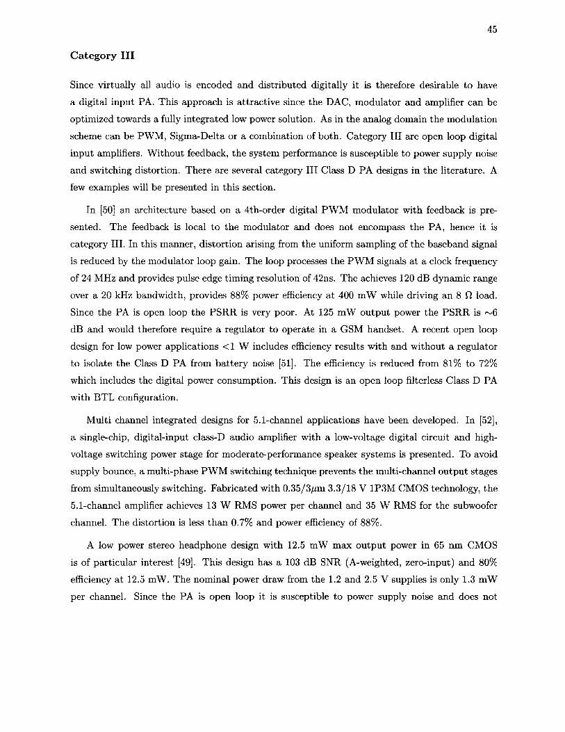
45
Category III
Since virtually all audio is encoded and distributed digitally it is therefore desirable to have
a digital input PA. This approach is attractive since the DAC, modulator and amplifier can be
optimized towards a fully integrated low power solution. As in the analog domain the modulation
scheme can be PWM, Sigma-Delta or a combination of both. Category III are open loop digital
input amplifiers. W ithout feedback, the system performance is susceptible to power supply noise
and switching distortion. There are several category III Class D PA designs in the literature. A
few examples will be presented in this section.
In [50] an architecture based on a 4th-order digital PW M modulator with feedback is pre
sented. The feedback is local to the modulator and does not encompass the PA, hence it is
category III. In this manner, distortion arising from the uniform sampling of the baseband signal
is reduced by the modulator loop gain. The loop processes the PW M signals at a clock frequency
of 24 MHz and provides pulse edge timing resolution of 42ns. The achieves 120 dB dynamic range
over a 20 kHz bandwidth, provides 88% power efficiency a t 400 mW while driving an 8 Q load.
Since the PA is open loop the PSRR is very poor. At 125 mW output power the PSRR is ~6
dB and would therefore require a regulator to operate in a GSM handset. A recent open loop
design for low power applications <1 W includes efficiency results with and without a regulator
to isolate the Class D PA from battery noise [51]. The efficiency is reduced from 81% to 72%
which includes the digital power consumption. This design is an open loop filterless Class D PA
with BTL configuration.
Multi channel integrated designs for 5.1-channel applications have been developed. In [52],
a single-chip, digital-input class-D audio amplifier with a low-voltage digital circuit and high-
voltage switching power stage for moderate-performance speaker systems is presented. To avoid
supply bounce, a multi-phase PW M switching technique prevents the multi-channel output stages
from simultaneously switching. Fabricated with 0.35/3/mi 3.3/18 V 1P3M CMOS technology, the
5.1-channel amplifier achieves 13 W RMS power per channel and 35 W RMS for the subwoofer
channel. The distortion is less than 0.7% and power efficiency of 88%.
A low power stereo headphone design with 12.5 mW max output power in 65 nm CMOS
is of particular interest [49]. This design has a 103 dB SNR (A-weighted, zero-input) and 80%
efficiency at 12.5 mW. The nominal power draw from the 1.2 and 2.5 V supplies is only 1.3 mW
per channel. Since the PA is open loop it is susceptible to power supply noise and does not

46
correct for errors in the switching stage. Furthermore, since the load is single ended rather then
differential (bridge tied load) there is virtually no power supply noise rejection.
A 350 mW output power PA yields an efficiency in the 66-79% range depending on the load
impedance [46]. The THD is on the order of 0.07% and maximum SNR is 74dB. The m odulator is
a single bit 3rd order EA with 128x oversampling. Another EA open loop Class D amplifier with
a multi-level MASH 2-2 modulator has been simulated in [47], The multi-level serves to reduce
the switching frequency but requires multiple power supplies and switches. For IC applications
the multiple power supplies are generally not available and multiple switches leads to increased
losses.
An open loop PW M based Class D amplifier has a power output 100 W [48]. Sophisticated
DSP algorithms are required to correct for the UPWM distortion and the digital PWM operates
a t a clock frequency of 196.6 MHz. To ensure the dynamic range is greater than lOOdB a timing
precision of better than 13ps is required.
Category IV
Category IV amplifiers have digital input and local analog feedback for the switching stage. These
topologies require an analog loop filter which consumes extra power and increases the overall noise
level. W ith a properly designed loop filter the need for a regulated power supply can be eliminated
and the switching stage can be directly connected to the battery terminals.
Category IV amplifiers usually use a second order analog loop filter consisting of two first
order integrators. Scaling to a new process requires redesign and verification.
A PWM Class D audio amplifier accommodates digital input with an integrated DAC config
ured to realize a direct connection between the DAC and the analog feedback loop [54]. Targeted
towards higher power applications in the 10-100 W range the power switching stage is located off-
chip. The published performance is; 0.0018% THD+N at 10 W output power, 0.004% THD+N
with 100 W output power and 113 dB dynamic range. The paper does not indicate which fabri
cation process was used nor any efficiency data. The unique feature here is the dual role of the
DAC reconstruction filter. The th ird order reconstruction filter converts the segmented current
DAC output to voltage and also acts as a loop filter for the feedback from the power stage to
improve linearity. While this reduces circuitry, it also adds complications in th a t the optimum
DAC reconstruction filter may not provide the optimum stability and loop bandwidth solution

47
for the amplifier. That is, it must improve linearity and provide good phase margin.
A fully integrated low-power 0.5 pm CMOS DAC and Class D PA with 70% efficiency is
presented in [53]. Here a single bit 5th order modulator is the PA driver. The PA has local
feedback for improved linearity. Since the modulator has single bit output it is amenable to
directly drive the PA, in this sense the output is treated as an analog signal. The PA analog loop
filter is second order integrator.
In [56] a digital input PWM amplifier with analog feedback implements a 7b flash converter
and third order integrating loop filter to digitally linearize the PA. This architecture is interesting
in tha t it has a low switching frequency of 375kHz and a fairly low 7b resolution ADC which
runs at twice the switching frequency. A discrete circuit implementation achieved a dynamic
range of 100 dB and THD of 85 dB. Issues to be resolved towards an IC implementation of this
architectures are the RC time constant ±5% tolerances for the third order error integrator, power
requirements for the flash ADC converter, pulse width jitte r sensitivity and loop stability due to
correction delays. There is also an unexplained increase in second order harmonic distortion tha t
needs to be addressed.
In [55] a class-D audio amplifier for mobile applications is fabricated in a 0.14pm CMOS.
The amplifier has a simple PDM based digital interface for audio and control. The audio system
consists of a Parser, Digital PWM controller, 1-bit DAC, analog feedback loop and the Class-D
power stage. W ith a 4 D load and output power of 3.4 W the PA efficiency is 90%. Two other
notable category III designs are [31] and [57].
Category V
Category V topologies deploy global feedback which encompasses the modulator, loop filter and
Class D PA. It corrects for power stage errors due to power supply noise, clock jitte r and switching
artifacts. In addition, modulator errors such as UPW M distortion will be corrected. This allows
the designer the ability to design a simple, low power modulator without sophisticated DSP
correction algorithms. The degree of error correction is determined by the loop filter design and
stability requirements.
A highly digital based architecture has two main advantages. First, the quiescent bias cur
rent associated with analog circuits is eliminated. Secondly, the design is readily scaled to new
fabrication processes. There are also other advantages such as yield. The performance of analog

48
circuits is susceptible to process variation which can lower overall yield.
Category V is highly scalable as both the modulator and loop filter are digital. The ADC
design in category V would be more complex then the analog loop filter in category IV, however
ADCs are commonly one of the first building blocks developed in new processes. This allows
for the opportunity to purchase the design from a third party and maintain a time to market
advantage relative to category IV.
While global feedback offers several desirable features and advantages, it receives modest
attention in the literature. The main disadvantage of global feedback is the requirement of a high
resolution ADC which impacts overall system efficiency. Furthermore, the ADC architecture has
significant impact on system performance, loop filter design and stability. Therefore, selecting
either an oversampling or Nyquist ADC must be considered in the initial design phase. To the best
of the authors knowledge the only global feedback related publications are [6] and this work [7,9].
Home stereo or multichannel audio applications typically specify a maximum of 200 W per
channel. Typical listening volumes be much lower then the maximum. A Class-D amplifier with
global feedback for home audio is presented in [6].
In this design the loop filter becomes a complex task to achieve acceptable performance. The
filter factors which have to be traded off include maximizing gain, EA ADC quantization noise
suppression and phase margin. The phase margin was 32° with a master clock operating at 19.66
MHz. The ADC was a high performance 24b EA which consuming a maximum power of 1 W [60].
The prototype achieved a THD+N of 0.001% with 15 W output to a 8 load. No efficiency
values are provided.
For headphone applications the target specifications are given in Table 3.1. For a global
feedback system with power output in the mW range, the ADC must be low power. The ADC
used in [6] is not feasible due to power consumption, frequency of operation and quantization
noise associated with the EA process [7,9]. The approach taken here is to slow the master clock
frequency to 2.822 MHz and use a low power SAR ADC.
3.4 .2 C om m ercial C lass-D A m plifiers
There are quite a few commercially available Class D amplifiers for low power applications.
Wolfson, Texas Instruments and Analog Devices all manufacture a variety Class D amplifiers for
low power applications. O utput power specifications range from 25 mW for headphones and 1-2

49
W for speakers. These designs are predominately analog input. Of interest here are the DAC
and PA integrated solutions with digital input.
Wolfson Microelectronics for example has two stereo DACs integrated with a headphone and
speaker amplifier. The headphone amplifier is a Class AB while the speaker driver is Class D.
The WM8986 is targeted to portable audio devices and is a fully integrated stereo DAC with
microphone preamps, headphone and speaker amplifier. The headphone driver provides. The
headphone driver provides 20 mW of power 20 mW with a THD+N of -70 dB. The Class D
speaker driver delivers 1 W with 87% efficiency. Analog Devices SSM2517 is a mono digital
input Class D amplifier. O utput power is 1.38 W into 8 Q with 92% efficiency and 1% THD+N.
Quiescent power consumption is 10.4 mW.
The Texas Instruments PCM1770 device is a CMOS, monolithic, integrated circuit which
includes DAC stereo converters, headphone circuitry, and support circuitry. The data sheet does
not specify the type of headphone amplifier but it appears to be Class AB. Maximum output
power with a 16 fl load is 13 mW per channel. There is no efficiency data provided however the
quiescent power consumption is 6.5 mW.
3.5 K ey Points
• The research is focused on low power headphone applications according to the specifications of Table 3.1.
• Distortion in pulse density modulation techniques is any perturbation in the waveform amplitude or timing.
• Open loop systems are susceptible to distortion. Closed loop systems are desensitized according to the loop gain.
• Techniques to linearize the PA include: negative feedback, indirect feedback, pre-distortion and feed forward.
• Switchmode power amplifiers require either EA, PWM or a hybrid combination of these modulation techniques.
• The literature summary has been subdivided into five categories. They are sorted according to input type (analog or digital) and feedback (open loop, local feedback or global feedback).

Chapter 4
System D esign
In this chapter a Class D amplifier topology with direct digital input for low power applications
is presented. Global feedback and a digital loop filter serve to correct errors and linearize the PA.
The main advantage being an inherent ability to scale the design to deep submicron processes with
minimal redesign effort in the analog domain. The digital core of the system is a high resolution
hybrid multi-bit EA-Pulse W idth Modulation (PWM) modulator without the need for Dynamic
Element Matching (DEM). Furthermore, DSP algorithms to correct for UPW M distortion are
not required due to the global feedback.
A prototype based on a FPGA and commercial 16b analog to digital converter (ADC) vali
dates the design principles. Prototype measurement results indicate greater than 30 dB of noise
rejection at 1 kHz with a discrete time Proportional plus Integral (PI) digital loop filter.
Portable audio devices such as MP3 players, tablets, smart-phones, laptops and wireless
headsets require good quality audio performance and optimum energy efficiency. A set of typical
specifications were given previously in in Table 3.1.
First, the system architecture under investigation is explained followed by a discussion on each
of main components. Simulation and measurement results based on a FPGA and commercial
ADC are presented.
4.1 System Architecture
The proposed topology shown in Fig. 4.1 consists of interpolation filters, digital loop filter, EA
modulator, PWM, Class D amplifier, low pass second order output filter, first order low pass
50
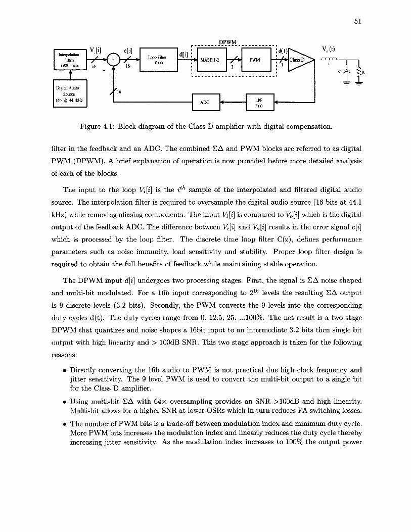
51
DPWMInterpolation
Filters OSR =64x
Digital Audio Source
16b @ 44.1kHz
V,[i] _ e[i]
16 N / i s
Loop Filter
r •
d[i] !M A SH 1-2
:<Kt)
C (z) Il«
/ *3 'A
««
V 0(t)
Class D
LPFAUUF(s)
Figure 4.1: Block diagram of the Class D amplifier with digital compensation.
filter in the feedback and an ADC. The combined EA and PWM blocks are referred to as digital
PWM (DPWM). A brief explanation of operation is now provided before more detailed analysis
of each of the blocks.
The input to the loop Vi[i] is the i th sample of the interpolated and filtered digital audio
source. The interpolation filter is required to oversample the digital audio source (16 bits at 44.1
kHz) while removing aliasing components. The input V)[i] is compared to V0[i\ which is the digital
output of the feedback ADC. The difference between Vi[i) and V0[i] results in the error signal e[i]
which is processed by the loop filter. The discrete time loop filter C(z), defines performance
parameters such as noise immunity, load sensitivity and stability. Proper loop filter design is
required to obtain the full benefits of feedback while maintaining stable operation.
The DPWM input d[i] undergoes two processing stages. First, the signal is EA noise shaped
and multi-bit modulated. For a 16b input corresponding to 216 levels the resulting EA output
is 9 discrete levels (3.2 bits). Secondly, the PW M converts the 9 levels into the corresponding
duty cycles d(t). The duty cycles range from 0, 12.5, 25, ...100%. The net result is a two stage
DPWM that quantizes and noise shapes a 16bit input to an intermediate 3.2 bits then single bit
output with high linearity and > lOOdB SNR. This two stage approach is taken for the following
reasons:
• Directly converting the 16b audio to PWM is not practical due high clock frequency and jitte r sensitivity. The 9 level PWM is used to convert the multi-bit output to a single bit for the Class D amplifier.
• Using multi-bit EA with 64 x oversampling provides an SNR > lOOdB and high linearity. Multi-bit allows for a higher SNR at lower OSRs which in turn reduces PA switching losses.
• The number of PWM bits is a trade-off between modulation index and minimum duty cycle. More PWM bits increases the modulation index and linearly reduces the duty cycle thereby increasing jitte r sensitivity. As the modulation index increases to 100% the output power

52
approaches full scale.
The DPWM single bit output is directly compatible with the Class D switching amplifier.
O ther DPWM examples include DC-DC converters [61] and an audio DAC [62] (uncompensated
open loop and no PA). The PWM output drives the Class D amplifier followed by a low pass
filter.
Since the discrete PW M process is not a true “natural” sampling process, harmonic distortion
will arise. However, since the modulator lies within a closed loop system the distortion will
be reduced according to the loop gain. This is advantageous in eliminating the need for DSP
interpolation algorithms as required as in [56], [15].
The most challenging aspect of this architecture is the ADC. It requires 16b precision at
a conversion rate of 2.822 MHz (64x oversampling) corresponding to the DPW M operating
frequency. In addition, low power operation is critical in maintaining the overall system efficiency
gained from the Class D amplifier.
An ADC can be either a Nyquist or EA type converter. Nyquist rate converters operate
slightly above the Nyquist rate and typically rely on precision matched components. On the other
hand, EA converters operate at much higher sample rates and in turn the matching precision
is relaxed [63]. The quantization and noise shaping associated with the EA process leads to
significant out of band noise peaking at f s/ 2. This noise can saturate the DPW M modulator and
cause loop instability. While this noise can be digitally filtered the filtering process introduces
loop delay, which in turn leads to reduced phase margin. Hence, though EA converters have
some advantages, they are not practical for this architecture.
In [6] a Class D amplifier with digital compensation incorporates a EA feedback ADC (Analog
Devices AD7760 20Msps 24b ADC which dissipates 1W). In this case the ADC output is not
decimated and filtered, the filtering is incorporated in the loop filter. Since the loop is operating
at a sample rate of 19.66 MHz some loop delay associated with filtering can be tolerated. In
addition, since ADC is operating at a very high OSR, the noise is shifted higher in frequency and
is easier to filter. Even so, the author acknowledges th a t a commercial version of the prototype
would require additional analog circuitry to contend with excessive quantization noise. While
this approach is acceptable for high output power applications on the order of several watts and
up its not a viable solution for low power applications.

Interpolation ► Filter Output
' h I n O S R - S n
Figure 4.2: Input and output spectrum of an ideal interpolation filter..
4 .1 .1 In terp o la tion F ilters
The function of the Interpolation Filter (IF) shown is twofold. Firstly, to increase the sampling
rate from / v (44.1 kHz) to O S R • /jv- This allows for noise shaping in the DPW M module.
Secondly, to suppress the spectral replicas and minimize the out of band power. This improves
the dynamic range of the control loop and relaxes the linearity requirements placed on the Class
D amplifier and analog low pass filter. This is due to reduced intermodulation distortion products
folding in band. The input and output spectrum of an ideal interpolation filter is shown in Fig.
4.2
Efficient Interpolation Filters (IF) are multi-stage structures. The IF upconverts the input
sample rate from / n to f s in multiple stages. In theory, it is possible to construct a single stage
filter tha t oversamples directly from /tv to f s however this would lead to a large complex digital
filter operating a t f s . This would be inefficient and could generate significant digital noise.
To obtain high efficiency the most complex filter with the highest tap count is implemented
at the lowest operating frequency. As an example consider a three stage IF. The first stage must
remove the first adjacent (between f s to 3 /# ) and subsequent odd order aliases. Therefore, the
first stage has the most stringent specifications and will be the most complex filter. W ith odd
order aliases removed the requirements and complexity of the second stage is reduced since the
remaining aliases are further apart and steep rolloff rejection is not required. The third and final
stage operates a t the highest frequency f s = O S R x / v and is usually a sample or zero order
hold. This results in a sine function response th a t adds further filtering. A three stage IF [64]
provides 64 x oversampling, a passband ripple of ±0.06dB and out of band attenuation of 43dB.
In the FPGA prototype to be presented no IF filters are used. The baseband audio signal is
L \ L I A

54
directly oversampled a t f s . A complete three stage IF filter design will be presented in a following
section.
4 .1 .2 D P W M
DPW M is the cascaded combination of the multi-bit EA and PWM highlighted in Fig. 4.1. The
DPWM converts a 16b input to a single bit output, in essence an ideal 16b PW M which is not
practical to implement directly. This two stage approach offers the following advantages,
• Multi-bit facilitates higher SNR and lower out of band noise a t reduced clock frequencies.
• EA provides high linearity
• PWM acts as a parallel to serial converter compatible with Class D switching amplifier.
Sigma D elta M odulation
A brief introduction to the operation of a first order single bit EA modulator was given in
Sec. 2.2.2. There are extensive variations EA modulators of different orders and either multi or
single bit. The tradeoffs between single and multi-bit EA modulators are as follows:
• Multi-bit quantization error is reduced by 6dB per bit added to the quantizer resolution. Therefore, an equal improvement in SNR and reduced out of band noise is achieved. The reduced out of band noise relaxes the requirements on the demodulating low pass filter.
• Since there is no filtering prior to the Class D amplifier a single bit modulator with high out of band noise is more likely to cause folding of the noise spectrum in the region around fa/2 into the signal band (DC to 20 kHz).
• Since multi-bit modulators generate less quantization noise they can achieve a given SNR specification at a lower OSR compared to single-bit modulators. As a result lower power operation may be achieved.
• Single bit is directly compatible with a Class D amplifier while multi-bit’s require additional circuitry. For example, a PW M which performs the parallel to serial conversion.
• Multi-bit modulators tend to be more stable over a larger range of input values. This allows for a higher modulation index.
• Multi-bit is less sensitive to clock jitte r due to lower clock frequency.
• Multi-bit element mismatches introduce an output error which will generate harmonic distortion as well as increased noise. One way to overcome this affect is to by spreading the energy of the harmonic spurs into pseudo-random noise using a technique called dynamic element matching [65]. Single-bit inherently does not have this problem.

55
150
100
L-2co35oezCO
L=1
50
128 256OSR
Figure 4.3: EA SNR calculations for L=1 to 4 with M=2.
The EA theoretical performance is determined by the oversampling ratio (OSR), noise shaping
loop filter order and number of output bits. The SNR can be calculated from [62],
SNR = (6L + 3) log2 O S R - (8L - 4) + 20 log10(M - 1) (4.1.1)
where L is the loop order, O S R is the oversampling ratio and M output levels. Fig. 4.3 is a plot
of (4.1.1) for L = 1 to 4 and M = 2 (single bit). For multilevel M >2 and the SNR is increased
according.
A popular topology which relaxes the stability requirements of higher order modulators is a
cascaded structure in which each subsequent stage processes the quantization error from the pre
ceding stage. This is commonly referred to as a MASH (M ulti-stAge noise-SHaping) modulator.
Fig. 4.4 is the block diagram of a modified version of the standard MASH 1-2 modulator [62].
The 1-2 nomenclature implies a first order loop filter followed by a second order, hence an overall
third order response. There are many other third order EA configurations however, the MASH
1-2 was selected to address challenges specifically related to this application. In particular,
• The signal transfer function can be made delay free so as not to degrade loop stability.
• All coefficients are unity or 1/2 which simplifies hardware implementation.
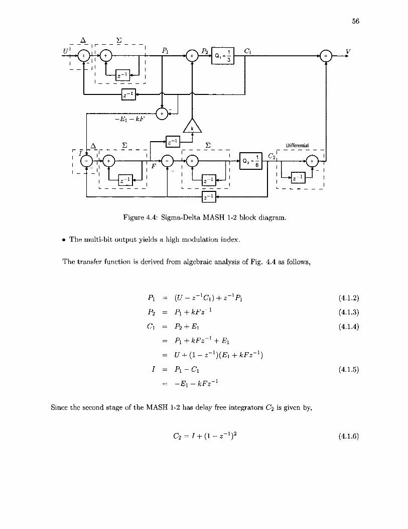
56
A
✓
D ifferential
-1
-1 . - 1
-1
-1
-1
Figure 4.4: Sigma-Delta MASH 1-2 block diagram.
• The multi-bit output yields a high modulation index.
The transfer function is derived from algebraic analysis of Fig. 4.4 as follows,
Pi = ( U - z - ' C J + z - ' P i
P2 = Px + k F z - 1
Cl = p 2 + e 1
= Pi + k F z ~ l + E l
= U + ( l - z - l ){Ei + k F z ~ l )
I = P i - C i
= - E i - k F z ~ l
Since the second stage of the MASH 1 -2 has delay free integrators C2 is given by,
C2 = / + ( l - £ ~ 1)2
(4.1.2)
(4.1.3)
(4.1.4)
(4.1.5)
(4.1.6)

57
and the overall output V(z) is,
V = Ci + ( l - z - l )C2 (4.1.7)
= U + (1 - + k F z - 1) + (1 - z~ l )[I + (1 - z - 1)2^ ]
= U + ( l - z ~ 1f E 2
from which we note the signal transfer function is unity and third order noise shaping has been
achieved.
The feedback path with scaling factor 0 < k < 1 is set so tha t the first integrator output of
the second stage isn’t overloaded [62]. A value of k = l / 2 was selected to optimize the modulation
index and efficient hardware implementation.
M odulation Index
Since the output power is limited by Pa = V 2/ R any reduction in output swing will reduce the
available power and SNR accordingly. This is especially im portant in low voltage applications
where voltage headroom is a t a premium and the modulation index must be optimized.
In Fig. 4.4, Qi — 1/3 which results in seven possible quantization values of C i=(-1, -2/3,
-1/3, 0, 1/3, 2/3, 1) likewise for Q2 = 1/6, C2= ( - l / 6 , 1/6). Overall the output will have a
total of 9 possible levels from -4/3 to + 4 /3 in 1/3 increments. Assuming an input range for
U of + /-1 the effect modulation index is the ratio of first quantizer C\ to the to tal quantizer
summation C* = C\ + C2 which in this case is Ci/Ct = 1/(4/3) or 75%. This results in 2.5dB
SNR degradation. Third order noise shaping can be achieved with three first order loop filters
in a MASH 1-1-1 configuration however this significantly degrades the modulation index and in
turn the SNR as Ct — C\ + C2 + C3 will increase and thereby decrease C\fCt-
M ASH 1-2 Simulations
The MASH 1-2 SNR and modulation index performance was verified in M atlab simulations. A
time domain plot is provided in Fig. 4.5 of a 10 kHz tone. Note th a t the quantization fractions
have been scaled to integer values. The top plot is output of first order modulator, C\. The
middle plot is the differentiated values of C2. The bottom plot is the final output V (z) with 9
integer values ranging from -4 to +4.

a) First order SDM output5
4
3
2
i l l1
0•1-2•3
-4
■5
2
1.5
1
0.5
0
-0.5
-1
-1 .5
-2
b) S e c o n d o rder SD M output
c) Overall M ash 1-2 output5
4
3
2
1
0•1
-2-3
-4
•50.1 0.2 0.3 0 .4 0 .5 0.6 0 .7 0.8 0.90 1
x 10
T im e o f fs e t 0
Figure 4.5: MASH 1-2 time domain plots for a 10 kHz input with a sample rate of 400ns (OSR=62.5): a) O utput of the first order sigma-delta, b) O utput of the second order sigma- delta, c) Overall third order noise shaped output obtained from the sum of plots a and b.
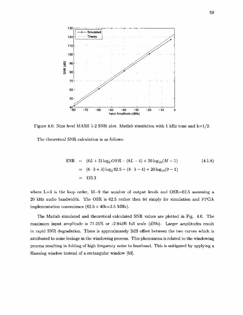
59
130SimulatedTheory120
110
100
mTJ,QLZw
-80 -70 -60 -50 -40 -30Input Amplitude (dBfs)
-20 -10
Figure 4.6: Nine level MASH 1-2 SNR plot. M atlab simulation with 1 kHz tone and k = l/2 .
The theoretical SNR calculation is as follows:
SNR = (6L + 3) log2 O S R — (8L — 4) + 20 log10(M — 1) (4.1.8)
= (6-3 + 3) log2 62.5 - (8 • 3 - 4) + 201og10(9 - 1)
= 123.3
where L=3 is the loop order, M =9 the number of output levels and OSR=62.5 assuming a
20 kHz audio bandwidth. The OSR is 62.5 rather then 64 simply for simulation and FPGA
implementation convenience (62.5 x 40k=2.5 MHz).
The M atlab simulated and theoretical calculated SNR values are plotted in Fig. 4.6. The
maximum input amplitude is 71.25% or -2.94dB full scale (dBfs). Larger amplitudes result
in rapid SNR degradation. There is approximately 2dB offset between the two curves which is
attributed to noise leakage in the windowing process. This phenomena is related to the windowing
process resulting in folding of high frequency noise to baseband. This is mitigated by applying a
Hanning window instead of a rectangular window [63].

60
DPWM
MASH 1-2 dt
Figure 4.7: PWM parallel to serial conversion process.
PW M
The PW M following the MASH 1-2 in Fig. 4.7 converts the multi-bit output to a single bit.
The conversion is accomplished by incrementally varying the duty cycle from 0 to 100% in 12.5%
increments according to the MASH 1-2 output. For example, with a clock frequency of 2.5 MHz
the clock period is 400 ns. For a MASH 1-2 output of V(z) = —1/3 the PWM duty cycle would
be 37.5% (high for 150 ns and low for 250 ns).
There are various implementations of digital PW M [66] each with various trade-offs in term s of
complexity, power consumption, linearity and sensitivity to process and environmental conditions.
A digital implementation of a PWM circuit was discussed in Chapter 2 Fig. 2.5. W ith low OSR’s
this circuit is not feasible due to high counter clock frequency and harmonic distortion, however
due to the high OSR and reduced number of bits from the MASH 1-2 modulator the circuit is
feasible in this application.
M ulti-bit Selection Criteria
The MASH is inherently multi-bit due to the summation of the cascaded modulators. The number
of bits at the MASH output is determined by the quantizer which determines the number of PWM
duty cycles. The trade-offs related to selecting the number of MASH quantizer bits are as follows,
• PWM Frequency: The MASH multi-bit output is transformed into a binary signal via the PW M module. More bits infers smaller pulse widths. This translates into increased clock jitte r sensitivity and higher PWM operating frequency.
• Modulation index: Modulation indices approaching 100% are ideal as both full scale SNR and maximum output power are achieved. The modulation index increases with the number of bits.
• SNR;: The in-band SNR; is the SNR within the audio band and for 16 bit audio is on the order of 96dB. SNR; increases with the number of bits according to (4.1.1).

61
• SNRq: The out of band SNRq is the ratio of the in-band signal (j20 kHz) to the integrated out of band noise (20 kHz to /<,/2). The out of band energy can give rise to intermodulation distortion within the audio band due to the switching stage non-linearity. Larger SNRo reduces the impact of this affect.
4.2 Control Loop Analysis
A closed loop control system with continuous and discrete time models is presented in this section.
The control loop is a classical negative feedback design. Negative feedback has several desirable
features such as,
• Improved linearity since any distortion introduced by the switching stage is reduced by the loop gain.
• Improved noise rejection. For example, supply or substrate or coupled noise be reduced by the loop gain.
• Reduced second order distortion due to mismatches in the pfet and nfet of the Class D switching stage.
• Reduced distortion inherent in the UPWM process.
• Reduced sensitivity to environmental conditions.
A closed loop system requires a loop filter (compensator) to ensure system stability with
sufficient phase margin. Further complicating the design is the mixed signal nature of the archi
tecture tha t requires mapping between the continuous ‘s’ and discrete ‘z’ domains. To design the
digital compensator a s-domain model of Fig. 4.1 is formulated and then transformed into the
z-domain. Fig. 4.8 is a linear model of the amplifier with feedback. The objective is to design
a compensation network C(s) to track the input and make the loop insensitive to external noise
sources and improve linearity. The remaining transfer functions are defined as follows: P(s) for
the pulse modulator DPWM, G(s) for the power stage and low pass filter transfer function, and
H(s) for the ADC.
Ultimately C(s) will be converted to an equivalent discrete model C(z) shown in Fig. 4.8b.
The approach taken here is to model the system using conventional control system theory in
continuous time and then convert C(s) into an equivalent discrete model C(z). This approach is
known as digital redesign [67]. The closed loop transfer function of the continuous time model is:
V0(s) CPG(s) Vi(s) 1 + CPGH(s) (4.2.1)

62
u(s) dfs)
Compensator Pulse Modulator Power stage
H(s)
P(s)C(s) G(s)
ADC
d(n)u[n]V,[n]
Compensator Power stagePulse Modulator
\ H(s)
P(z)C(z) G(s)
ADC
Figure 4.8: Feedback compensation model a) Continuous time model, b) Mixed signal model digital redesign
and the loop gain T(s) is the cascaded gain of all stages in the loop,
T{s) = C{s)P(s)G{s)H{s). (4.2.2)
The loop response to additive noise is determined by solving for the transfer function at
injection node. The noise could be distortion caused by a non-linearity in the switching stage,
variation in the PWM duty cycle or power supply ripple for example. Noise injected in the
forward rif(s) and reverse nr (s) paths are analyzed in Fig. 4.9. Setting n r (s)=0 and V)=0 the
transfer function for noise injected in the forward path is,

63
T l f ( s )
d(s)u(s)
Compensator Pulse Modulator Power stage
H(s)
P(S)C(s) G(s)
ADC
Figure 4.9: Forward and reverse noise injection loop analysis
V0{s) G(s)(4.2.3)
rif(s) 1 + T ( s ) '
Thus for large loop gain |T(s)| 1 the noise appearing a t the output is attenuated. Setting
rif(s)= 0 and 1^=0 the transfer function for noise injected in the feedback (reverse) path is,
Vo(s) -1 T(s)(4.2.4)
n r(s) H ( s ) l + T(s)
Assuming ]T(s)| 1 the noise transfer function will be proportional to 1 /H(s) which is a
constant. As a result (4.2.4) offers little or no noise reduction.
4 .2 .1 C ontinuous to D iscrete T im e
Initially, the loop analysis is based on continuous s-domain models for all transfer functions.
Subsequently, once the loop has been compensated and stabilized, the loop filter C(s) is converted
to a z-domain model C(z). The pole-zero matching method is accurate and is relatively insensitive
to coefficient variations [68].
The rules governing the pole-zero transformation method of an arbitrary transfer function
C(s) are [67]:
1. If C(s) has a pole at s = —ap + j u p, then the discrete equivalent C(z) has a pole at

64
SpectrumAnalyzerHP3585A
N oisesource D iffam p
Altera Stratix FPGA
SINE ROM LUT
Analog Devices ADC AD7621
Loop Filter
C(z)DPWM
P(z)20MHz
LPF F (s)2.5MHz A D C H (s)2.5M H zPLL
Figure 4.10: Prototype hardware and measurement implementation.
z = eS aP+JUJpY1's; where Ts is the period of the sampling frequency.
2. If C(s) has a zero at s = — a z + j u z , then the discrete equivalent C(z) has a zero at2 _ e ( ~ a z +juiz )Ts
3. All zero’s at s = oo are mapped to the point z = — 1.
4. A unit delay is represented by z ~ x.
5. The gains are matched at band center or similar critical point such as DC and is selected
such tha t <7(5)15=0 = C(z)\z=\.
4.3 System Prototype
The prototype shown in Fig. 4.10 consists of a FPGA, ADC, signal generator to model a noise
source and a differential amplifier to buffer the output for spectrum analyzer measurements.
The compensator and modulator functionality are implemented in the Altera Stratix FPGA. A
commercial 16b ADC from Analog Devices is used in the feedback path. The power stage and
filtering are implemented with dual low pass filtered opamps.
A Class D amplifier usually has a second order low pass LC filter connected to the load. In the
FPGA prototype it was convenient to use opamps as buffers and filters but they are not capable
of driving low impedance loads. In this case, the distortion from the Class D switching stage is
omitted in the model. Therefore, to measure the loop response a calibrated tone is injected into

65
the loop in both the open and close loop cases. The loop response can then be determined by
comparing the output of the open and closed loop measurements.
The DPWM and ADC transfer functions are unity and delay free P (s )= l and H (s)= l, re
spectively. The opamp first order LPF corners a t 25 kHz and scales the FPGA PW M output to
levels compatible with the ADC. The transfer function is given by:
m = ^
where a — 0.64 is an amplitude scaling factor for the ADC and [3 = 5.67 x 10~6 sets the corner
frequency.
The compensator C(s) characteristics are specified from Bode plot analysis of the control loop
transfer functions. The FPGA DPWM P(s) output is low pass filtered adding 90° phase shift to
the loop. A lag compensator [69] of the form,
C{s) = Cc(l + — ) (4.3.2)s
is sufficient to verify system performance. This type of compensator increases the loop gain
such tha t the output is better regulated at frequencies below /x, and is also referred to as a
proportional-plus-integral, or PI controller. Increased loop gain is beneficial towards improved
noise immunity however, the tradeoff is increased loop bandwidth.
Based on Bode plot analysis C0 = 8 and /x = 10 kHz increased the loop gain and conserva
tively limited the closed loop bandwidth to 1/20 of the switching frequency to avoid feedback
of the switching ripple [70]. Pole-zero matching [67] transforms C(s) -» C(z) which can then be
implemented as a digital filter. Applying pole-zero matching to (4.3.2) with f s = 2.5 MHz the
z-domain transfer function becomes,
, 8.125 — 7.875z~1 .C(z) = ------ --- j (4.3.3)
1 — z x
where the the coefficients have been rounded to the nearest binary fraction to simplify hardware
implementation.

66
Open loop frequency response
T(s) C(s) F(s)
-20
-40T T
40- T ( s ) - C(s)
T(s) delayed
-80
-100
-12010k 100k 1M100 1k
Frequency (Hz)
Figure 4.11: FPGA prototype open loop frequency response assuming H (s)= l and P (s)= l
4 .3 .1 B od e P lo t A n alysis
A Bode plot of the open loop network is given in Fig. 4.11. The transfer function of the DPWM
modulator P(s) and ADC H(s) are assumed to be unity. The transfer functions for the LPF F(s)
and compensator C(s) responses are added to get the overall loop gain T(s). The unity gain
frequency for T(s) occurs at 141.5 kHz. The phase margin a t unity gain is 97° however, this does
not take into account the ADC sampling delay. The ADC sampling (zero order hold) in effect
adds 1/2 clock cycle [29] loop delay and therefore reduces the phase margin. At 2.5 MHz the net
phase margin is 87° as indicated by the delayed T(s) phase plot.
The closed loop transfer function is plotted in Fig. 4.12. The magnitude variation over the
audio band is less than 1 dB. The 3 dB corner frequency occurs at 122 kHz.

Mag
nitu
de
(dB
)
Closed loop frequency response
-10
-1 5
-2020
o> -2 0<DX3
-8 0
-10010k 100k 1M100 1k
Frequency(Hz)
Figure 4.12: FPGA prototype closed loop frequency response assuming H (s)= l and P(s)

68
4 .3 .2 A D C
The ADC requires 16b resolution and a conversion rate of 2.82 MHz. For the prototype, an Analog
Devices AD7621 16b Successive Approximation Register (SAR) ADC met the requirements. In
addition, it does not add shaped quantization noise like a EA converter would. While suitable
for FPGA system verification, the AD7621 consumes 70 mW which is excessive for low power
applications.
In order to address this limitation, a low power ADC architecture will be introduced in
following chapters. For the time being the objective is to perform system level verification with
the AD7621.
4.3 .3 S im ulations
The mixed signal system was modelled in Simulink. For simulation purposes the interpolation
filters were bypassed by directly oversampling the input tone. The LPF was modelled as a linear
transfer function given by (4.3.1) and an ideal ADC modelled by a 16b quantizer and zero order
hold. The clock frequency for the simulations was 2.5 MHz.
Simulation FFT results at the output of the MASH 1-2 and LPF in closed loop operation
are plotted in Fig. 4.13. For a -6dBfs input the SNR at the LPF output is 109 dB (full scale
input SNR=115dB). Though the Simulink model is linear, harmonic distortion arises due to the
discrete PWM sampling process. While the even order harmonics are suppressed differentially,
the odd order harmonics are reduced by the loop gain. Hence, while distortion is observed at
the output of the MASH 1-2 within the loop it is subsequently suppressed a t the output due to
feedback.
4 .3 .4 M easurem en ts
The hardware for mono operation is given in Fig. 4.10. The prototype uses an A ltera Stratix
FPGA and external test boards for the opamps and ADC. Though no power stage is implemented,
the hardware is sufficient to test the system architecture and loop dynamics.
The ability of the loop to reject noise, such as tha t from the power supply or compensate for
distortion in the switching stage is set by the loop gain. Since the DPWM P(s) and ADC H(s)
are ideally unity gain the loop gain is set by the compensator C(s) and LPF F(s) as:

69
-100
i \>Afr \kiyr
MASH 1-2
25kFrequency (Hz)
Figure 4.13: FFT plot a t the output of the MASH 1-2 and differential LPF. P lot obtained with f s=2.5 MHz and applying a hanning window.
m = I (4.3 4)V,( ,) 1 + C(s)F(s) 1 '
where Vf(s) is a noise source in the forward path of the loop. Fig. 4.14 is a plot of the theoretical,
simulated and measured loop response. The measurement was performed by injecting a tone into
one of the opamps and comparing the open and closed loop responses on a spectrum analyzer.
The results are in generally good agreement with some discrepancy due to the pole-zero mapping
process and coefficient quantization.
The results of Fig. 4.14 indicate the control loops ability to reduce power supply noise and non
linear switching effects. Furthermore, the non-linear effects associated with UPW M sampling [14]
are also reduced. This avoids the need for complex high speed DSP algorithms to synthesize low
distortion PW M when generated outside the loop as in [56]. The final plot of Fig. 4.15 is the
measured differential PW M output with a 1 kHz input tone. Both the differential output and
feedback help to suppress harmonics.
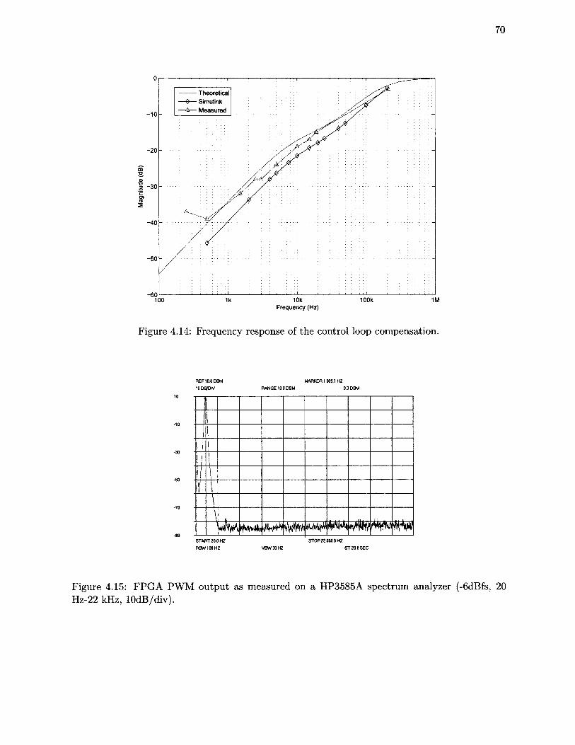
70
T h e o re tic a l
-6— S im ulink
-A— M e a s u re d-10
-20
1 - 3 0
- 4 0
- 5 0
- 6 010k
F re q u e n c y (H z)1 0 0 k 1M100
Figure 4.14: Frequency response of the control loop compensation.
REF 100 DBM MARKER 1 0091 HZ
10DB/DIV RANGE 100 DBM 3.3 DBM
10
'10
•30
-50
-70
-90START 200 HZ
RSW100HZ
Figure 4.15: FPGA PWM output as measured on a HP3585A spectrum analyzer (-6dBfs, 20 Hz-22 kHz, lOdB/div).
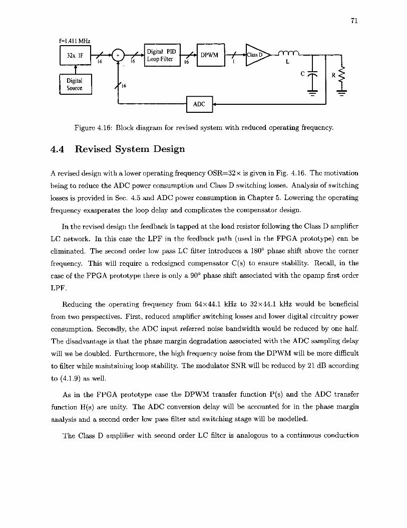
71
f = 1.411 MHz
16 16C lassD
ADC
32x IF DPWM
DigitalSource
Digital P1D Loop Filter
Figure 4.16: Block diagram for revised system with reduced operating frequency.
4.4 Revised System Design
A revised design with a lower operating frequency OSR=32x is given in Fig. 4.16. The motivation
being to reduce the ADC power consumption and Class D switching losses. Analysis of switching
losses is provided in Sec. 4.5 and ADC power consumption in Chapter 5. Lowering the operating
frequency exasperates the loop delay and complicates the compensator design.
In the revised design the feedback is tapped at the load resistor following the Class D amplifier
LC network. In this case the LPF in the feedback path (used in the FPGA prototype) can be
eliminated. The second order low pass LC filter introduces a 180° phase shift above the corner
frequency. This will require a redesigned compensator C(s) to ensure stability. Recall, in the
case of the FPGA prototype there is only a 90° phase shift associated with the opamp first order
LPF.
Reducing the operating frequency from 64x44.1 kHz to 32x44.1 kHz would be beneficial
from two perspectives. First, reduced amplifier switching losses and lower digital circuitry power
consumption. Secondly, the ADC input referred noise bandwidth would be reduced by one half.
The disadvantage is tha t the phase margin degradation associated with the ADC sampling delay
will we be doubled. Furthermore, the high frequency noise from the DPWM will be more difficult
to filter while maintaining loop stability. The modulator SNR will be reduced by 21 dB according
to (4.1.9) as well.
As in the FPGA prototype case the DPWM transfer function P(s) and the ADC transfer
function H(s) are unity. The ADC conversion delay will be accounted for in the phase margin
analysis and a second order low pass filter and switching stage will be modelled.
The Class D amplifier with second order LC filter is analogous to a continuous conduction
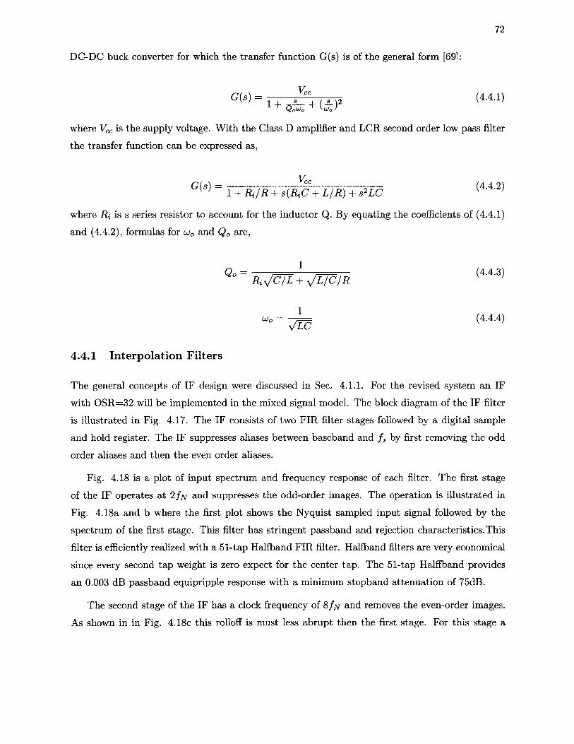
72
DC-DC buck converter for which the transfer function G(s) is of the general form [69]:
G(«) = ; Y “ , , , , (4.4.1)1 + 5 i ; + ( s ) 2
where Vcc is the supply voltage. W ith the Class D amplifier and LCR second order low pass filter
the transfer function can be expressed as,
° ^ = 1 + R i/R + s(R iC + L /R ) + s2L C
where Ri is s series resistor to account for the inductor Q. By equating the coefficients of (4.4.1)
and (4.4.2), formulas for uia and Q0 are,
Q° ~ H.v'CTL- yrL jC !R (4'4'3)
= v a {4AA}
4.4 .1 In terp o la tion F ilters
The general concepts of IF design were discussed in Sec. 4.1.1. For the revised system an IF
with OSR=32 will be implemented in the mixed signal model. The block diagram of the IF filter
is illustrated in Fig. 4.17. The IF consists of two FIR filter stages followed by a digital sample
and hold register. The IF suppresses aliases between baseband and f s by first removing the odd
order aliases and then the even order aliases.
Fig. 4.18 is a plot of input spectrum and frequency response of each filter. The first stage
of the IF operates at 2 / at and suppresses the odd-order images. The operation is illustrated in
Fig. 4.18a and b where the first plot shows the Nyquist sampled input signal followed by the
spectrum of the first stage. This filter has stringent passband and rejection characteristics.This
filter is efficiently realized with a 51-tap Halfband FIR filter. Halfband filters are very economical
since every second tap weight is zero expect for the center tap. The 51-tap Halffband provides
an 0.003 dB passband equipripple response with a minimum stopband attenuation of 75dB.
The second stage of the IF has a clock frequency of 8 / a t and removes the even-order images.
As shown in in Fig. 4.18c this rolloff is must less abrupt then the first stage. For this stage a

73
/ „ =40 kHz 2 /„ * /» / s = 32 fN
d) S/Hc) LPF FIR 4x
b) Halfband FIR 2x
e) Output 16-bit @ 1.28MHz
a) Input 16-bit @ 40kHz
51 taps 25 taps
Figure 4.17: Block diagram of OSR=32 interpolation filter a) Baseband input spectrum, b) Halfband FIR 2x, c) LPF FIR 4x, d) S/H 4x, e) cascaded output.
25-tap LPF FIR filter provided a minimum of 70dB stopband attenuation and 0.36dB passband
ripple.
Finally, a digital sample and hold register operating at 32 Jn provides some extra sine function
filtering as shown in Fig. 4.18d. The cascaded IF response is illustrated in Fig. 4.18e.
4.4 .2 P ID C om p en sator
A PID compensator is comprised of a PD and PI transfer function. Each serves a specific purpose
in shaping the open loop magnitude and phase response. The role of each is as follows,
• PD is a proportional-plus-derivative or lead transfer function tha t is used to increase phase margin. A zero is added to the loop gain far below the crossover (unity gain) frequency such tha t the phase margin is increased. A pole above the crossover frequency is added to limit the gain of the zero.
• PI is a proportional-plus-integral or lag transfer function tha t increases low frequency loop gain such tha t the output is better regulated from DC to frequencies well below the crossover frequency. An inverted zero is added well below the crossover frequency.
PID (proportional, integral, derivative) controllers are common in compensating second order
systems. The PID controller incorporates aspects of both PI and PD controllers to improve phase
margin and low frequency regulation.
The first step is to calculate the parameters which define the transfer functions with component
values L=10 uH, C=5.23 uF, R=32 D, and Rj = 0.2Q (derived from inductor Q). These standard
components values th a t can be obtained in a 0805 package. From (4.4.3), (4.4.4) Q0=5.3 and
fo ~ 22 kHz respectively.

Mag
nitu
de
(dB
)
74
a) 1 ' 1 11
.....J....... ... . 1 1 i I I I i 1 11 1 1 1 1 ... ..... ........T---------
» . . . . ) / ...................... \ U ........ \ 1 r r..
mmtnmihm I I i i
-20-40-60-80
0-20-40-60-80
0-20-40-60-80 r \ / - \
150100 200 250 300Frequency (kHz)
Figure 4.18: Interpolation Filter frequency response, a) Baseband input spectrum, b) Halfband FIR 2x, c) LPF FIR 4x, d) S/H 4x, e) cascaded output.

75
The PID was designed in an iterative process to optimize the phase margin and while increas
ing the loop gain. For the PD controller
P D (s) = (4.4.5)1 + s / Up
where fco=10.72, f z=37.7 kHz and f p=525.6 kHz. The PI controller transfer function is
P I(s) = l + ^ f (4-4.6)
where the inverted zero f iZ= 10 kHz. Substituting ka, f z , f p, f i z and multiply PD and PI to get
PID,
X n n , x 4.52 x 10"5s2 + 13.56s + 6.734 x 10⁵ C ( s ) = P W ( S) = P D (S) P m = -----------g(3-028 x 10~7, + 1)----------- <4 A 7 >
The PID transfer function is then converted to a discrete model using the pole-zero matching
technique resulting in,
, 61.08 - 108.9Z-1 + 48.32z-2C(2) = 1 - L 0 7 6 ,-i + 'o:d7576*-2 <4'4 '8)
4 .4 .3 S im ulations
The system will be simulation in two steps. The first step will be fundamental Bode plot analysis
based on the s-domain transfer functions. This will be followed by Simulink simulations to verify
the mixed signal model operation.
The Bode plot of the open loop gain T(s) is given in Fig. 4.19. Note th a t the continuous
model exhibits a phase margin of 58° at the crossover frequency of 141 kHz however, the actual
mixed signal phase margin is 38° due to the ADC sampling delay. The closed loop frequency
response is given in Fig. 4.20 where the corner frequency occurs a t 225 kHz.
The mixed signal model was then simulated in Simulink. In this manner system functionality
such as SNR and noise immunity is verified. The baseband input to the IF filters is a 20 kHz
bandwidth sampled at 40 kHz. W ith an OSR=32 the loop operating frequency is 1.28 MHz. Using
the DPWM as in the FPGA prototype the maximum SNR calculated from (4.1.1) is SNR= 102.3
dB.
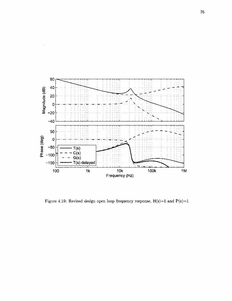
60
m 40"Oo' 20TJ
«+-»c 005012 -20
•40
05
TJ T(s)" " C(s)
- G (s)i - ioo
T(s) delayed- 1 5 0
100 1k 10k 100k 1MFrequency (Hz)
Figure 4.19: Revised design open loop frequency response, H (s)= l and P (s )= l

Mag
nitu
de
(dB
)
77
20
0
-20
-40
ro -100
-150
100 1k 10k 100k 1MFrequency (Hz)
Figure 4.20: Revised design closed loop frequency response, H (s)= l and P (s)= l
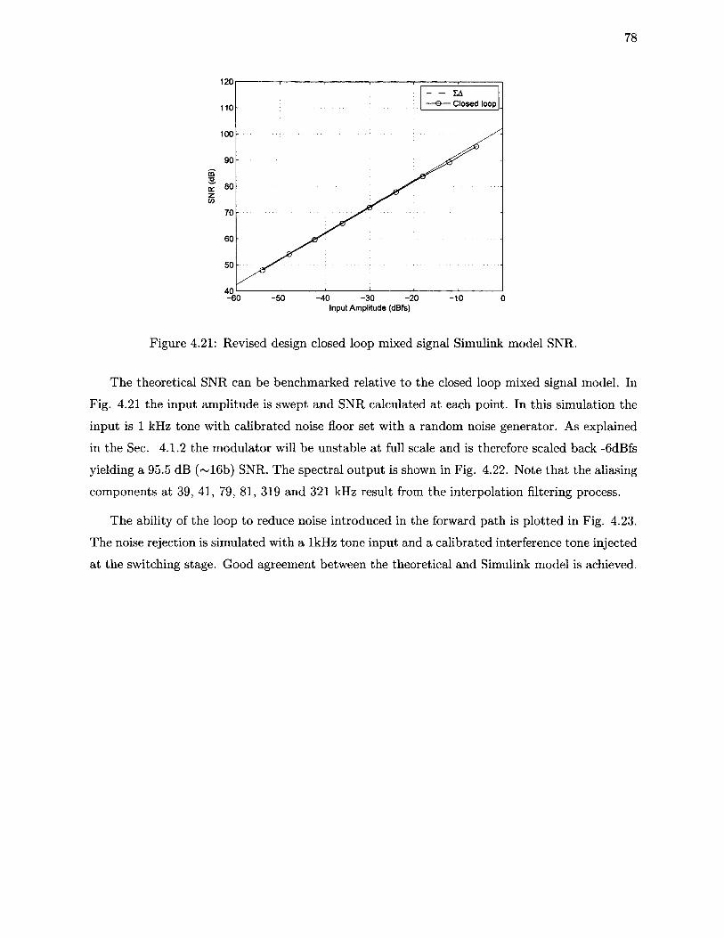
78
120 I A-e— Closed loop110
100
mT3a.zV)
6 0
4 0 L - 6 0 - 5 0 - 4 0 - 3 0 -20 -10 0
Input Amplitude (dBfs)
Figure 4.21: Revised design closed loop mixed signal Simulink model SNR.
The theoretical SNR can be benchmarked relative to the closed loop mixed signal model. In
Fig. 4.21 the input amplitude is swept and SNR calculated a t each point. In this simulation the
input is 1 kHz tone with calibrated noise floor set with a random noise generator. As explained
in the Sec. 4.1.2 the modulator will be unstable at full scale and is therefore scaled back -6dBfs
yielding a 95.5 dB (~16b) SNR. The spectral output is shown in Fig. 4.22. Note tha t the aliasing
components at 39, 41, 79, 81, 319 and 321 kHz result from the interpolation filtering process.
The ability of the loop to reduce noise introduced in the forward path is plotted in Fig. 4.23.
The noise rejection is simulated with a 1kHz tone input and a calibrated interference tone injected
at the switching stage. Good agreement between the theoretical and Simulink model is achieved.

79
03TJ<DTJ3 - 5 0
aE<
2(0Eo - 1 0 0 z
- 1 5 0100 10 k
F r e q u e n c y (H z)1 0 0 k 1M
Figure 4.22: Revised design closed loop spectral output.
20T h e o re t ic a lS im u lin k
10
0
-10
-20
- 3 0
- 4 0
- 5 0
- 6 01 0 k100 1k 1 0 0 k 1M
F r e q u e n c y (H z )
Figure 4.23: Revised design forward path noise suppression.

80
DriverPower stage
n t
iFigure 4.24: Class D amplifier consisting of a driver and power stage.
4. 5 CMOS Class D
An unloaded Class D amplifier is shown in Fig. 4.24. It consists of a driver stage and power stage.
The power stage is a large inverter capable of driving the 16 or 32 Q headphone impedance with
minimal losses. Since the power stage is a large device, a series of tapered inverters is required
to switch it efficiently. The series of tapered inverters is referred to as the driver stage.
The amplifier losses can be divided into switching Ps and conduction Pc losses. The total
power loss is defined as,
Pt = Pc + Ps . (4.5.1)
The switching losses are related to the charging and discharging of the MOSFET gate capac
itance during each switching cycle. When analyzing the switching losses there is no load on the
power stage. Conduction losses are related to I2Ron of a loaded power stage. These two losses
will be examined independently and then summed to determine to tal loss.
4.5 .1 S w itch in g losses
Tapered buffers have traditionally been analyzed from a digital perspective in terms of minimizing
propagation delays. A summary of the publications related to propagation modelling can be found
in [71]. Since current CMOS technology operates in the GHz range, significantly higher then the
application here, the propagation delay is of less interest then the switching losses.

81
The most common taper ratio [72] is,
(4.5.2)
which can be associated to the gate capacitance by the MOSFET dimensions,
k = CoxL(Wn + W p CoxL(W * +
W% + Wg W * + W*
(4.5.3)
where W% represents the gate width of a particular transistor. The subscript x = n or p refers
to either a nfet or pfet device respectively. The superscript y = p or d refers to the power stage
or first stage of the tapered buffer driver respectively.
The power stage dimensions are W p=4mm and W p=1.76mm with minimum length L=0.13
gm. The sizing matches the gm of the devices and provides low channel resistance Rds ~0.8 Q
to minimize conduction losses. The objective is to design the driver with optimum taper ratio k
in order to minimize switching losses. The switching energy (Joules) per cycle can be calculated
from,
and falling transition edges and virtually zero a t other times.
To find the optimum tapering ratio the switching losses for various tapering ratios have been
simulated with W p=1.76m, Wp =4rnm, W]f=160nm, W p=400nm . The rise/fall time and energy
are plotted in Fig. 4.25. The rise/fall time decreases with the taper ratio as the size mismatch
between adjacent inverters is reduced. At the same time the energy per cycle of the power stage is
reduced however, the driver energy is increasing. These two opposing trends suggest an optimum
taper ratio is attainable.
The faster rise/fall time lowers the energy in the power stage since there is less time for simul
taneous nfet and pfet conduction. The driver energy steadily increases due to increased capacitive
loading. The net result is an optimum tapering ratio of n=6 beyond which the power stage energy
reduction experiences diminishing returns and is offset by increased energy consumption of the
driver.
where T is one period of the switching cycle. Note th a t i(t) is significant only during the rising

82
400a) Power Stage Rise/Fall Time
4 5n taper stages
b) Energy per cycle160
-A— Driver -9— Power -*— Total
120
100Q.
> .E?<Dc
LU
40
20
2 3 4 5 6 7n taper stages
Figure 4.25: Simulation of Class D amplifier, a) Average 10% to 90% rise/fall time, b) Energy per switching cycle.
W ith the optimum taper ratio determined the power dissipation as a function of frequency
can be calculated from,
PS(W ) = ^ (4.5.5)
where T is the period of one switching cycle and is plotted in Fig. 4.26.
4 .5 .2 C on d u ction losses
Unlike switching losses, conduction losses are not a function of frequency. If the rise/fall time is
a negligible fraction of the switching cycle then the R^s impedance transition is assumed to be
instantaneous. The conduction losses take into account the resistive losses associated with the
channel resistance Rds and interconnect wiring losses Rw such tha t the total resistance is,
R on = R d s + R w - (4.5.6)
The conduction losses for a differential bridge tied load is calculated from,

83
Switching losses Ps300
2 5 0
_ 200
I 1 5 0
100
Frequency (MHz)
Figure 4.26: Total switching losses of the driver and power stage as a function of frequency.
p<= ( 4 - <4-5-7>
where Ri is the load impedance (16 Q or 32 f2) and Pto is the to tal power dissipated in the
resistors.
4 .5 .3 T otal losses
The to tal losses include both the switching and conduction losses. Depending on the frequency
of operation and power output either the switching or conduction losses can dominate. As an
example calculate the losses for a Class D amplifier with the following specifications,
• Differential bridge tied load
• (Wn=1.76mm, Wp=4mm)
• Driver taper ratio n=6
• R d s —0 . 8 f t
• R w=0.4 Q,
• R i = 32 Q
• f=2.82 MHz
• Pfo=100uW
84
From Fig. 4.26 with an operating frequency of 2.82 MHz the switching losses are 77 uW per
amplifier or 154 uW for a bridge tied load. The conduction losses are then calculated from (4.5.7)
to be Pc= 7 uW. In this case the switching losses are predominate and the total losses according
to (4.5.1),
p t = p c + p s = 154 + 7 = 161uW (4.5.8)
4.6 K ey Points
The design, simulation and construction of a digital input closed loop Class D amplifier has been
presented. Some key points of the design are as follows:
• A prototype operating at 2.5 MHz was constructed with an Altera FPGA, Analog Devices 16b SAR ADC and dual low pass filtered opamps.
• Noise injection measurements were performed and were in good agreement with theoretical predictions. At 1 kHz the noise rejection is 34dB
• The DPWM consists of multi-bit £ A and PWM hybrid configuration. Any distortion arising from the modulator is compensated by the loop gain.
• the closed loop was analyzed in the frequency domain using phase margin analysis. The continuous time transfer functions were then converted to the discrete time domain using the pole zero matching technique.
• A revised system design was proposed operating at half the frequency of the prototype. The goal being to reduce overall power consumption. This design was simulated in Simulink but not prototyped.
• The Class D amplifier losses consist of switching and conduction losses. Switching losses are frequency dependant and conduction losses are frequency independent.

Chapter 5
Low Power ADC D esign
As highlighted in Chapter 4 the quantization noise arising from the EA process complicates the
process of feedback design. The approach taken here is to use a Nyquist type data converter
which avoids the noise shaping process. Of particular interest is a specific Successive Approxi
mation Register (SAR) ADC with programmable thresholds. While this architecture alleviates
the quantization noise restriction, other significant challenges arise.
This chapter begins with an explanation of the generic SAR algorithm followed by a new
implementation approach. Simulation and analytical calculations for key design parameters such
as gain, common mode noise rejection, RMS input referred noise, resolution and tuning range are
presented. In addition, design challenges are discussed.
5.1 SAR Algorithm
ADCs are categorized as either Nyquist or EA type. A Nyquist rate converter operates slightly
above the Nyquist rate and typically relies on precision matched components. On the other
hand, EA converters operate at much higher sample rates and in turn the matching precision is
relaxed [63]. EA converters fundamentally involve quantization and noise shaping. This leads
to significant out of band noise peaking a t /s /2 . Though the noise can be digitally filtered, the
filtering introduces delay. In a closed loop application such as this, the delay leads to reduced
phase margin and potential instability. Hence, though EA converters are preferred, they are
problematic for closed loop Class D systems. In light of this, a Nyquist type ADC is proposed for
this application. In particular, a Successive Approximation Register (SAR) ADC is investigated.
SAR ADCs are frequently selected for medium to high resolution applications (8 to 16b) with
85
86
moderate conversion rates (up to 5 Msps) requiring low power consumption. As a result SAR
ADCs are ideal for a wide variety of portable battery operated applications.
The SAR ADC utilizes a binary search algorithm. Therefore, while the internal circuitry may
be running at several Megahertz (MHz), the actual ADC sample rate is 1/N of tha t number
where N is the resolution or number of converter bits.
The SAR algorithm flowchart is given in Fig. 5.1 where the input is assumed to be within
±.Vref/2. Upon assertion of the start signal the input Vin is sampled and the DAC output is set
to OV. The comparator then determines the signal polarity with the resulting bi= 0 or 1 sign bit
stored. Consequently, the next bit is determined by setting Vo AC = Vref / 4 or —Vref / 4 for &i=l
or 0, respectively. Likewise, the process repeats in total N times while adjusting the DAC at each
iteration by a factor of ±Vrej / 2 l+1 accordingly. At the end of the conversion cycle the N-bits
stored in the SAR are a valid digital representation of the analog input.
Two SAR circuit block diagrams are shown in Fig. 5.2. The conventional approach is shown in
Fig. 5.2a which is a direct implementation of the flowchart. For this architecture the resolution
is typically limited by the DAC linearity. Process and mismatch errors generally dictate tha t
converters with a resolution of 12 bits or higher will require laser trimming and/or a calibration
procedure.
An alternative approach is proposed in Fig. 5.2b where the DAC has been replaced by a
comparator with programmable offsets. The offset or threshold voltage, represents the tipping
point of the comparator. Shifting the offset voltage V0ff is analogous to the functionality of
setting Vdac- In essence, V0fr replaces Vdac in accordance with Fig. 5.1.
One way to create offsets is by introducing intentional mismatch or asymmetry in a differential
circuit. In conventional circuit design asymmetry is highly undesirable due to degradation of the
Common Mode Rejection Ratio (CMRR). Thus, while introducing intentional offsets a degraded
CMRR is one penalty of this approach.
Multiple forms of mismatch techniques are combined to allow both coarse and fine offset tuning
to within a fraction of a LSB. The manner in which these offsets are generated and selected is
explained in the following sections.
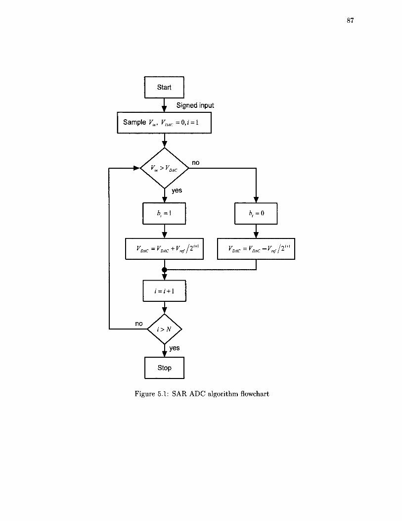
87
Signed input
noV > VV in ' ' DAC
yes
Start
1 = 1 + 1
V - V —V / l i+l¥ DAC V DAC ¥ re f / A= V + F / 2 ,’+iDAC ¥ DAC ^ ¥ re f j ^
Sample v „ VDAC = 0,i = l
Figure 5.1: SAR ADC algorithm flowchart

88
Start
Status
AnalogVin
DAC
ComparatorVref
N-bit DAC
Output
Track/Hold
Timing
Successive Approximation Register and control logic
a) Conventional SAR ADC functional block diagram.
Start
Status
AnalogVin
Voff
O
Track/Hold
Timing
Successive Approximation Register and control logic
b) Offset configurable SAR ADC functional block diagram.
Figure 5.2: Conventional and alternative SAR ADC block diagrams.

89
5.2 COP A D C Architecture
The concept and design specifics of a Configurable Offset with Preamplifier (COP) SAR ADC
or simply COP ADC are now introduced. The COP ADC shown in Fig. 5.3 is a more detailed
circuit diagram of the system shown in Fig. 5.2b. It is meant to operate in accordance to the
process flow of Fig. 5.1 where Vdac has been replaced by V0ff which is variable. In this section
the progression to circuit level implementation is made.
The COP ADC consists of input track and hold capacitors, an array of preamplifiers with
fixed offsets, a high resolution low power comparator and digital circuitry for calibration and
successive approximation. In addition to the preamplifier array, the comparator has a series of
offset mechanisms tha t can be digitally controlled, hence the COP acronym.
Preampssw
Comparator
preamp offsetholdtrackcompoffset
Clock comp clockSAR Control Logic
comp output
Figure 5.3: COP SAR ADC block diagram
An im portant aspect of the design is the method in which the offsets are generated. The
preamplifier offsets are configurable in ±30 mV steps while the comparator has three offset
controls. The comparator steps are ±8 mV, ±316 and ±16 ^V. Overall, the four offset
settings are independently controlled and can be superimposed to generate any desired offset
limited by the smallest step size (16 /iV).
The target specifications for the COP ADC are listed in Table 5.1. The conversion rate is

90
set according to the DPWM frequency of 64x44.1 kHz or 2.82 Msps. Likewise, the comparator
frequency is 16x2.82 Msps or 45.16 MHz. The input voltage swing is 2.4 Vpp which is the
maximum swing across the load assuming a 1.2 V supply. The maximum swing will never be
achieved due to saturation limit of the DPW M. A more practical swing of 1.6 Vpp would provide
lOmW of power to a 320 load without saturating the DPWM. The ADC power dissipation will
dominate the overall system budget. To the best of the authors knowledge the commercial ADC
with comparable specifications and lowest power consumption is the Analog Devices AD7985 16b
SAR. The AD7985 datasheet specifies a power consumption of 28mW at a sample rate of 2.5
Msps.
The input referred noise is a critical spec. It is calculated from simulations by integrating the
input referred noise from DC to one half the sample frequency (in this case 22.58 MHz). The
noise consists of both thermal and flicker noise contributions. The end result is tha t excessive
noise will result in comparator errors. Since noise reduction entails increased power requirements
it is im portant to specify the noise correctly.
The probability of errors is determined from the ratio of the integrated noise to the lsb.
Assuming a Gaussian noise distribution the lsb voltage step size should be 6 to 7 time the
rms noise voltage [73]. In this case the probability of comparator error is less then 10-9 when
lsb=6enojse, ie. the probability the noise exceeds 6 standard deviations. Here, enotse is the
integrated input referred noise of the cascaded preamplifier and comparator. This is a stringent
requirement of which the impact on SNR is not clearly defined.
It has been demonstrated for SAR ADCs the noise specification can be relaxed to l/21sb with
the addition of an extra comparator iteration [74], In this approach for the first N iterations the
SAR operates in a high noise state wherein enoi5e=l/21sb and then for an extra error correction
iteration N + l it operates in the low noise state where enmse=l/41sb. This only slightly increases
the overall power consumption. Based on measurement results SNR, INL and DNL specifications
are published rather than noise specifications.
The following sections explain in each circuit in more detail. Note tha t the fabricated inte
grated circuit consists of the preamplifiers and comparator which form the core of the COP ADC.
The track and hold has been omitted and the ADC control logic can be implemented in a FPGA
for maximum flexibility.
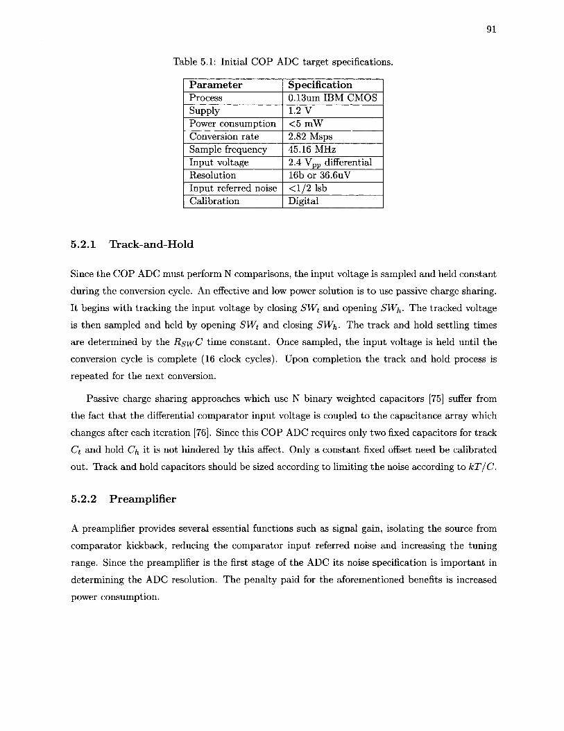
91
Table 5.1: Initial COP ADC target specifications.
Parameter SpecificationProcess 0.13um IBM CMOSSupply 1.2 VPower consumption <5 mWConversion rate 2.82 MspsSample frequency 45.16 MHzInput voltage 2.4 Vpp differentialResolution 16b or 36.6uVInput referred noise < 1/2 lsbCalibration Digital
5.2 .1 Track-and-H old
Since the COP ADC must perform N comparisons, the input voltage is sampled and held constant
during the conversion cycle. An effective and low power solution is to use passive charge sharing.
It begins with tracking the input voltage by closing SW t and opening SW}t. The tracked voltage
is then sampled and held by opening SW t and closing SW \ . The track and hold settling times
are determined by the R sw C time constant. Once sampled, the input voltage is held until the
conversion cycle is complete (16 clock cycles). Upon completion the track and hold process is
repeated for the next conversion.
Passive charge sharing approaches which use N binary weighted capacitors [75] suffer from
the fact tha t the differential comparator input voltage is coupled to the capacitance array which
changes after each iteration [76]. Since this COP ADC requires only two fixed capacitors for track
Ct and hold Ch it is not hindered by this affect. Only a constant fixed offset need be calibrated
out. Track and hold capacitors should be sized according to limiting the noise according to kT jC .
5.2 .2 Pream plifier
A preamplifier provides several essential functions such as signal gain, isolating the source from
comparator kickback, reducing the comparator input referred noise and increasing the tuning
range. Since the preamplifier is the first stage of the ADC its noise specification is im portant in
determining the ADC resolution. The penalty paid for the aforementioned benefits is increased
power consumption.

92
vn O
Vi2 O
O Vo\
O Vo2
Figure 5.4: Differential amplifier.
The COP ADC has an array of preamplifiers, all connected to a common resistive load. The
array consists of a balanced differential pair and several intentionally mismatched differential
pairs. The mismatches are intentional so as to produced an array of linear offset voltages. The
drawback of this approach is compromised common mode noise rejection.
In the following section analytical expressions are derived for gain, common mode noise re
jection and offset voltage. The formulas are then shown to provide very good agreement with
simulation results. In addition, flicker and thermal noise contributions are discussed and simu
lated.
Gain and Rejection Ratios
We begin with defining the gain parameters for a generic amplifier in terms of common and
differential mode voltages. Subsequently, a differential pair CMOS amplifiers is analyzed to
derive gain and noise rejection parameters. Equivalent half circuit models for the common and
differential modes take into account mismatches and simplify the analysis. Using this approach
gain and rejection ratio formulas are derived.
Based on small signal analysis, several performance parameters of the differential pair amplifier
can be derived. Small signal analysis is valid for signal levels in which the resulting nonlinearity
is insignificant. The differential amplifier of Fig. 5.4 can be characterized in terms of its common
and differential mode input and output. The differential mode input and output are defined as,
Vid — V n Vj2 (5.2.1)
Vod — V0 l V02 ■ (5.2.2)
The input and output common mode are defined as,

93
Vic —Vil + Vi2 (5.2.3)
Vol + Vo2 (5.2.4)
The general equations defining the gain param eters for a differential amplifier [10] are,
Vod — A d m V id ^ c m —dm^ic (5.2.5)
Vqc — Adm—cmVid T A riri V'l (5.2.6)
from which four gain parameters can be extracted. The differential mode voltage gain Adm relates
the change in the differential output to differential input. This is the desired voltage gain:
Adm —VodV{d
(5.2.7)Vic—0
The common mode voltage gain A cm relates the voltage change in the common mode output to
common mode input:
A — (5.2.8)Vid=0
The differential mode to common mode voltage gain Adm-cm relates the change in the common
mode output to differential mode input:
Ad/,Vid
(5.2.9)Vic—0
The common mode to differential mode voltage gain ^4cm-dm relates the change in the differential
mode output to common mode input:
A c m —dmVod
V ic(5.2.10)
i>id=0
94
A differential amplifier amplifies differential input signals while rejecting any changes in its
common mode input. Common mode noise needs to be sufficiently suppressed otherwise it can
propagate and degrade the performance of subsequent stages. Common mode noise may originate
from a variety of sources such as the power supply or substrate coupling. The differential voltage
gain Adm, should therefore be much larger then the gain parameters of (5.2.8)-(5.2.10).
For a perfectly symmetric amplifier with pure differential input (Vic = 0) the output is
purely differential (voc = 0), therefore Adm-cm — 0. Likewise, in a perfectly symmetric am
plifier Acm—dm = 0, however symmetry alone does not guaranty Acm = 0. Rejection ratios can
be defined to quantify susceptibility to undesirable noise. The most prevalent of which is the
Common-Mode-Rejection-Ratio (CMRR) defined as:
C M R R = Adm (5.2.11)
Similarly, the Differential to Common mode Rejection Ratio (DCRR) and Common mode to
Differential mode Rejection Ratio (CDRR) are defined as:
D C R R AdmA d m —c
(5.2.12)
C D R R = AdnA,cm—dm
(5.2.13)
An unbalanced amplifier with a non-zero Adm-cm will generate some common mode output
for a pure differential input. While not desirable this will have minimal impact on latter circuits
which can reject the common mode component according to the CMRR. Of more concern is
a non-zero Acm-dm in which a common mode input is converted to a differential output. The
resulting differential output will be indistinguishable from the desired signal and therefore cannot
be rejected by subsequent stages.
Due to process and mismatch variation practical amplifiers will exhibit some degree of asym
metry which results in non-zero Adm-cm > and A crn. In this particular application, mis
match is deliberately introduced thereby further exasperating the problem. As a result, the
rejection ratio performance will be degraded. Thus the gain parameters must be calculated or
simulated to determine their impact on overall system performance.

95
Vcc
M2M l
tail 'tail
Figure 5.5: Source coupled differential pair amplifier.
The direct approach to calculate the gain terms is to analyze the complete small signal equiv
alent circuit of Fig. 5.5. Alternatively, exact half circuit analysis is possible if the cross coupled
gain terms Adm-cm and A cm-dm are taken into account [10]. Using this approach the mismatch
in gm, 9mb and ra have been taken in account while assuming a matched load resistance R. Based
on the analysis in Appendix A the derived gain equations are:
G lAcm-dm = R -1 (5.2.14)
Ol 2
R {—Ar0{R + r0)Agm - AgmR A r 0 + A gmA rl)■A dm—cm — (5.2.15)
-R (A g mr0{R + ra) + R A gmA r 0 - gmA r 20) /c o 1 2*cra — (5.2.16)
G2
Adm = R ^ ~ (5.2.17)lOL2
where,

96
Cll — 4r0Agm(i? + ra + 2Rtan (l 4* 9mb^o)) 4~ &9mAgmT0Rta.il (5.2.18)
4A r0gm (R 4~ ^Rtail) 4“ (A9m 4~ ‘‘9mbRtail^9mb)
« 2 = 4:(R + r a)(R + r a + 2Rtan (l + (gm + 9mb)ro)) (5.2.19)
-\-2RRtail{^9m 4" A<7m;,)Ar0 (1 4" 2{9m 4" 9 m b )R ta i l)o
a 3 = -A.r0{Ag nr0R.taii 4- 2gm (R + r0 + 2Rtau + 2gmbr0R taii) (5.2.20)
Rtail^9m {^9m 4“ Apmft)) 2(i? + 2i?£aji)A g^A r0
4~(4<?mi?iaiZ 4- 2<7m(l + 2gmbRto.il) ~ Rtail^9m {^9m 4“ A^mb))Aro
The difference and average param eter values are defined as,
A9m — 9 m M l 9m M 2
A rQ = f o M l - r oM2
^ 9 m b = 9 m b M \ 9mbM2
9m = i .9m M l 4- 9 m M 2 ) j C‘
r0 = (r0Ml 4- rGM2)/2
9mb = (9m bM 1 4- 9 m b M 2 ) /2
(5.2.21)
(5.2.22)
Offset Voltage
The COP ADC uses an array of preamps like tha t of Fig. 5.5 with intentional differential pair
mismatch to generate offsets. The amplifiers are connected in parallel though only one is active
a t any instance in time. Assuming a matched load R, the differential input referred offset voltage
Vio, can be derived from DC analysis to equalize the diff pair drain currents [10] given as,
14, = AF, + ^ <5 -2 -23>V V 1 + 2{W /L) V 1 W L) )
where the average and difference quantities are defined as,
A (W /L ) = (W /L )\ - (W /L )2 (5.2.24)
97
{W/L) = (W/L), + (W/L), 2
(5.2.25)
AVt = Vn - Vt2 (5.2.26)
= Vg + V 2 2
(5.2.27)
For small mismatches (5.2.23) can be approximated by the simplified equation,
Vio = A Vt - Vgs - Vt A (W /L )2 ' (W /L )
(5.2.28)
Noise
The preamplifier is the first stage in the COP ADC, hence its noise contribution is significant in
the overall system performance. Though the comparator stage can contribute significant noise as
well, its contribution is reduced by the preamplifier gain.
The dominant noise sources in active fets are thermal and flicker noise. The input referred
therm al and flicker noise spectral densities (V 2/H z ) are given by [77],
• k is dependant on device characteristics and can vary significantly for devices within the same process,
• k is Boltzmann’s constant 1.38 x 10~23 J /K ,
• T is the temperature in Kelvin,
• W is the device width,
• L is the device length,
• Cox is the gate capacitance per unit area.
• gm is the transconductance
+ W L C oxfK
(5.2.29)
where
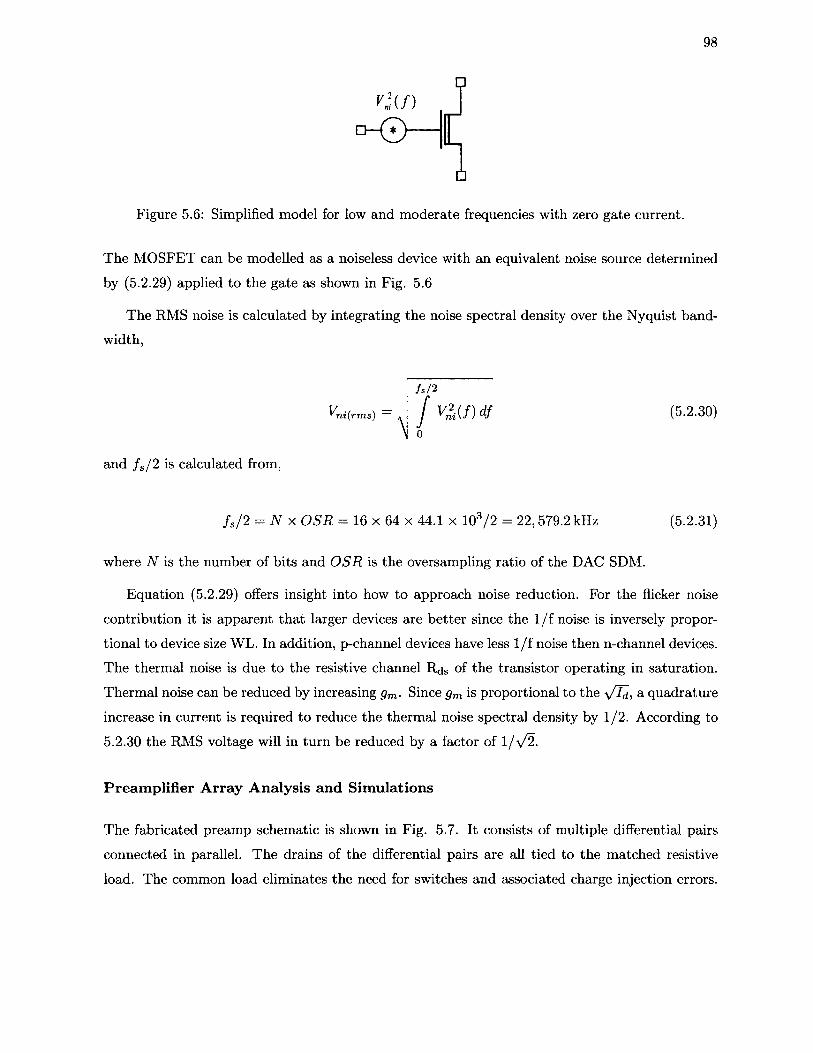
98
v - ( f )
°-©— r□
Figure 5.6: Simplified model for low and moderate frequencies with zero gate current.
The MOSFET can be modelled as a noiseless device with an equivalent noise source determined
by (5.2.29) applied to the gate as shown in Fig. 5.6
The RMS noise is calculated by integrating the noise spectral density over the Nyquist band
width,
Vrn i ( r m s )
\
f s / 2
J K , i f ) i f (5.2.30)
and f s/2 is calculated from,
f s/2 = N x O S R = 16 x 64 x 44.1 x 103/2 = 22,579.2 kHz (5.2.31)
where N is the number of bits and O SR is the oversampling ratio of the DAC SDM.
Equation (5.2.29) offers insight into how to approach noise reduction. For the flicker noise
contribution it is apparent tha t larger devices are better since the 1 /f noise is inversely propor
tional to device size WL. In addition, p-channel devices have less 1 /f noise then n-channel devices.
The thermal noise is due to the resistive channel Ras of the transistor operating in saturation.
Thermal noise can be reduced by increasing gm. Since gm is proportional to the y/Ta, a quadrature
increase in current is required to reduce the thermal noise spectral density by 1/2. According to
5.2.30 the RMS voltage will in turn be reduced by a factor of l/y /2 .
Preamplifier Array Analysis and Simulations
The fabricated preamp schematic is shown in Fig. 5.7. It consists of multiple differential pairs
connected in parallel. The drains of the differential pairs are all tied to the matched resistive
load. The common load eliminates the need for switches and associated charge injection errors.

99
O Vd2VdiO
O Vg2M2Ml
I r e f
M4 M3
Figure 5.7: Preamplifier schematic.
The array consists of a matched differential pair and several intentionally mismatched pairs.
These mismatched pairs introduce both positive and negative offsets to extend the COP ADC
tuning range. During the conversion cycle the COP ADC algorithm dictates which one of the
preamplifiers is enabled at any given time.
Table 5.2 lists the preamp array design param eters valid for a bias current of Ibias=T-25mA
and load resistance R=750fh In total there are 9 preamps in the array, the 5 listed plus another
4 which swap W \ and W-i of preamps 1-4. This provides both positive and negative offset tuning.
The small signal differential voltage gain Adm calculated using (5.2.17) is plotted Fig. 5.8a.
In addition, the unbalanced and balanced conditions have been simulated. These two conditions
Table 5.2: Preamplifier array device parameters(Vcc=1.2V, R=750fi and Ibias=l-25m A).Preamp W i
(fim)W 2
(pm)Sml(mS)
Sm2(mS)
Srofcl(mS)
Sm62(mS)
r0im
r02(Q)
Rtail(ft)
0 152 152 11.29 11.29 1.75 1.75 3103 3103 15651 192 112 13.89 8.67 2.17 1.34 2373 4266 15652 224 80 16.02 6.47 2.53 0.99 1931 5970 15503 248 56 17.69 4.70 2.81 0.72 1627 8489 15314 264 40 18.84 3.45 3.01 0.53 1408 11850 1531

1 0 0
exist due to the introduction of intentional device mismatch. Unbalanced refers to the case where
the common mode voltage results in unequal bias current distribution (/^(Mi) 7 ^d{Mi))- In the
balanced case the gate voltages have been adjusted to counter the offset voltage and divide the
bias current equally {Id(Mi) — Id{M2 ))• Depending on the input voltage and SAR algorithm, the
preamp may be in either the balanced or unbalanced state. The balanced/unbalanced terminology
is not to be confused with device mismatch.
The remaining gain param eters are plotted in Fig. 5.8b. This plot contains both simulated and
calculated values using (5.2.14)-(5.2.16). While A crn is insensitive to mismatch both A*m_cm and
Acm-dm. increase in a somewhat linear fashion. Thus, designs with intentional device mismatch
pose additional challenges compared to the matched case where these terms tend to zero. Fig.
5.9 is a plot of the rejection ratios according to formulas (5.2.11)-(5.2.13) and expressed in dB.
Recall tha t the gain parameters were derived assuming a small signal model. Simulations
indicate tha t the rejection ratios are fairly constant up to the 3 db compression point, tha t is the
input amplitude where the small signal gain A^m is 3 dB lower. For input amplitudes up to the 3
dB compression point the CMRR, DCRR and CDRR degrade on the order of 1 to 3 dB. Beyond
the compression point the further degradation is observed.
The simulated and calculated (5.2.23) input referred offsets are plotted in Fig. 5.10. The
formula derived from the DC analysis using the square law formula tends to underestimate the
simulation results based on the more accurate BSIM model. The preamp array is designed to
provide 30mV steps over a range of ±120mV. This represents the largest offset adjustment in the
COP ADC.
The simulated balanced and unbalanced input referred noise results are plotted in Fig. 5.11
for both the 50 MHz and 25 MHz comparator clock frequency. The frequency will depend on
the control system selection and DPW M oversampling ratio which will either be 16 • 64 • 44.1
kHz=45.16 MHz or 16 • 32 • 44.1 kHz=22.58 MHz respectively. The chosen 50 MHz and 25 MHz
frequencies are rounded values convenient for subsequent simulations which include the clocked
comparator. The continuous time preamplifier does not require a clock, the clock frequency
simply sets the noise bandwidth of interest. Therefore, the noise is either integrated from DC to
25 or 12.5 MHz accordingly.
Assuming a white spectral noise density, the integrated RMS noise would be reduced by a
factor of y/2 or approximately 30% for a bandwidth reduction of 50%. In Fig. 5.11 for the matched

Gain
(V/V
)
1 0 1
(a) Differential Gain A .' ' d m
— b— Unbalanced * Calculated
- 0 - Balanced
- e
mT3Cto0
2.5 3.50.5Preamp
(b) Gain Parameters0.3
d m cm
cm0.25cm d m
Calculated
0.15
0.1
0.05
0.5 2.5 3.5Preamp
Figure 5.8: Preamplifier simulated and calculated a) differential gain Adm, b) rejection ratios for the preamplifier array.
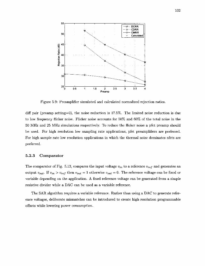
1 0 2
V — DCRR -9— CDRR -0— CMRR * Calculated
0.5 2.5 3.5Preamp
Figure 5.9: Preamplifier simulated and calculated normalized rejection ratios.
diff pair (preamp setting=0), the noise reduction is 17.5%. The limited noise reduction is due
to low frequency flicker noise. Flicker noise accounts for 50% and 60% of the total noise in the
50 MHz and 25 MHz simulations respectively. To reduce the flicker noise a pfet preamp should
be used. For high resolution low sampling rate applications, pfet preamplifiers are preferred.
For high sample rate low resolution applications in which the thermal noise dominates nfets are
preferred.
5 .2 .3 C om parator
The comparator of Fig. 5.12, compares the input voltage Vin to a reference vref and generates an
output V o u t■ If V in > v r e f then V o u t = 1 otherwise v ^ t = 0. The reference voltage can be fixed or
variable depending on the application. A fixed reference voltage can be generated from a simple
resistive divider while a DAC can be used as a variable reference.
The SAR algorithm requires a variable reference. Rather than using a DAC to generate refer
ence voltages, deliberate mismatches can be introduced to create high resolution programmable
offsets while lowering power consumption.

Inpu
t re
ferre
d no
ise
V (u
V)
103
Preamplifier input reffered offset120
— calculated -©— simulated
100
|o
2T©o3Q.C 40
0.5 2.5 3.5Preamp setting
Figure 5.10: Preamplifier simulated and calculated input referred offsets.
Preamp integrated noise
-0— unbalanced 50MHz -0— balanced 50MHz v - unbalanced 25MHz b - balanced 25MHz
nr
2.5 3.50.5Preamp setting
Figure 5.11: Preamplifier simulated input referred noise.

104
Reference voltages
Variable
Figure 5.12: Comparator with variable and fixed reference voltages.
Latched Comparator
One particular comparator architecture or latch type voltage sense amplifier as it is also referred
to [2], is shown in Fig. 5.13 along with corresponding device sizes in Table 5.3. I t features a
differential input pair (M l,2) feeding a current into a pair of inverters (M3,4 and M5,6) in a
positive feedback configuration. In this manner a large gain is created and any small difference
a t the input of M l,2 is rapidly amplified to full logic levels a t the output. The sense amplifier is
used in several digital applications which are summarized in [78]. Often it is used in inpu t/ou tpu t
circuits as a low power alternative to rail-to-rail logic.
The transient response of the comparator output nodes are sketched in Fig. 5.14. The elk
signal controls the operating modes. When elk is low the comparator is in reset mode and when
its high the comparator is in the comparison or evaluation mode. When elk is low transistors
M7-M10 are switched on and nodes X i, X 2 , VQ\ and V0 2 are pulled high. Nodes X \ and X 2 are
charged according to the time constant R m C xi 2 where Ron is the on resistance of M7 or M10 and
C x i) C x2 represent the to tal parasitic capacitive loading at X \, X 2 respectively. During reset,
the comparator core is inactive, its memory is cleared and it draws virtually no current from the
Table 5.3: Latched comparator device sizes.Parameter M l M2 M3,5 M4,6 M7-10 M il
(^m) ( H (/xm) ( H w (Aim)W 51 51 10 2 2 .5 10 5L 0.14 0.14 0.14 0.14 0 .1 2 0.14

105
elkelk elkM4 M 6
M8 M9 M10M7
V..OOV,
M3 M5
M2M l
elkM il
Figure 5.13: Latch type voltage sense amplifier [2],
supply. When elk goes high the comparator senses the differential input Vn — Vj2 and the output
is set accordingly to full logic levels by the positive feedback configured pair of inverters (M3,4
and M5,6).
The non-linear behavior of the latch comparator results in the transistors operating in different
regions. During the comparison mode, its possible for the transistors to operate in, or transition
from, the subthreshold, triode or saturation regions. As a result, the small signal param eters are
continuously varying. Therefore, it is convenient to linearize the circuit during different phases
of operation where the small signal param eters are assumed to be constant. The phase transition
is considered to be instantaneous, however precise definitions of the edges is unknown and must
therefore be approximated [79].
The comparison mode can be divided into three phases. Phase 1 commences upon the rising
edge of elk, M l and M2 are in saturation and the cross coupled inverters are inactive. Nodes X \,
X? and output nodes V0j and V„2 are pulled high from the reset mode. Any voltage difference
between Vn and V& causes an imbalance in the drain currents of M l and M2. As a result, nodes
X \ and X ‘2 discharge at different rates.

106
a>O)roo>
Figure 5.14: Transient response of the output nodes during reset and compare clock phases.
Phase 2 occurs when either X \ or X 2 discharges to Vcc — V r n 3 ,5 > where Vrn3,5 is the threshold
voltage of M3 or M5 which, as an approximation, are considered equal. Now M l,M2, M3 and
M5 are in saturation. At this point M3,5 start to conduct and generate a voltage difference at
the output V0i and V02 - Nodes X \_2 continue to discharge towards zero volts and nodes V0i, V02
discharge towards Vcc — \VTpA,%\-
In phase 3 only the cross coupled inverters are active as the positive feedback rapidly amplifies
the initial differential input voltage to full logic levels. Here M l,2 are no longer in saturation as
the node voltages X \ and X 2 tend to zero. As a result M l and M2 exert no further influence on the
decision process. Subsequently, the output reaches a steady state condition with complimentary
output logic levels and no further current is drawn from the supply.
O ffset C o n fig u ra tio n
One of the design challenges of the sense amplifier or comparator as it shall be referred to, is
contending with the inevitable device mismatches which shift the comparator tripping point. This
Reset Compare
Time
107
shift is known as an offset voltage. Given a mismatch between M l and M2, the drain voltages
will exhibit different slew rates due to current imbalance, hence an offset is created. One method
to null the offset is to capacitively load the drains of M l,2 to counter the current imbalance.
This technique was first used in [80] where up to ±120mV of offset in 8mV steps was achieved.
Moreover, the trimming capacitors were uniquely implemented using 4-bit binary weighted PMOS
devices as parasitic capacitors on the drains of M l,2.
Rather than trying to null the offset, subsequent research exploited the mismatch effect in
ADC designs. A n-bit flash ADC consists of 2n comparators each of which requires a unique
reference voltage. The core of a 4b 1.25GS/s flash ADC [81] consists of 15 comparators each
with intentionally mismatched input pairs. These mismatches eliminate the need for a resistor
ladder network. Furthermore, each comparator is calibrated to within 1/4 LSB using the binary
weighted PMOS trimming capacitor technique adapted from [80]. W ith a 200mVpi>c]iff input
range each offset is 12.5mV and can be calibrated to within 3mV with the 16 binary weighted
PMOS trimming capacitors.
The SAR algorithm compares the input to a DAC generated reference voltage multiple times.
Each time the DAC voltage is adjusted up or down in a binary weighted fashion depending
on the comparator output. Here, the DAC has been replaced by reference “voltages” th a t are
programmable precision offsets. These offsets are created by two methods. The first method is
to intentionally mismatch the input pair M l,2 by a factor A W [81], [82]. This will create an
imbalance in drain currents of M l and M2 at the onset of the comparison cycle. From (5.2.28),
assuming tha t both devices have the same gate length and threshold voltage, the input referred
offset with mismatch A W = W\ — W2 is approximately,
<5'2'32>
Furthermore, multiple mismatched differential pairs can be connected in parallel and individually
enabled. In this manner, a sequence of linearly spaced offsets can be obtained. The array consists
of a matched differential pair, two pairs for positive offsets and two pairs for negative offsets. The
device dimensions are specified in Table 5.4.
The second method is to vary the capacitive load Cvar tied to the drains M l,2 [80]. The
difference A C = (CvartM 1 — Cvar,M2 ) must be compensated A I — (Im i ~ I M2 ) during the initial
slewing of the comparison phase. This is a useful technique for fine tuning the offset according
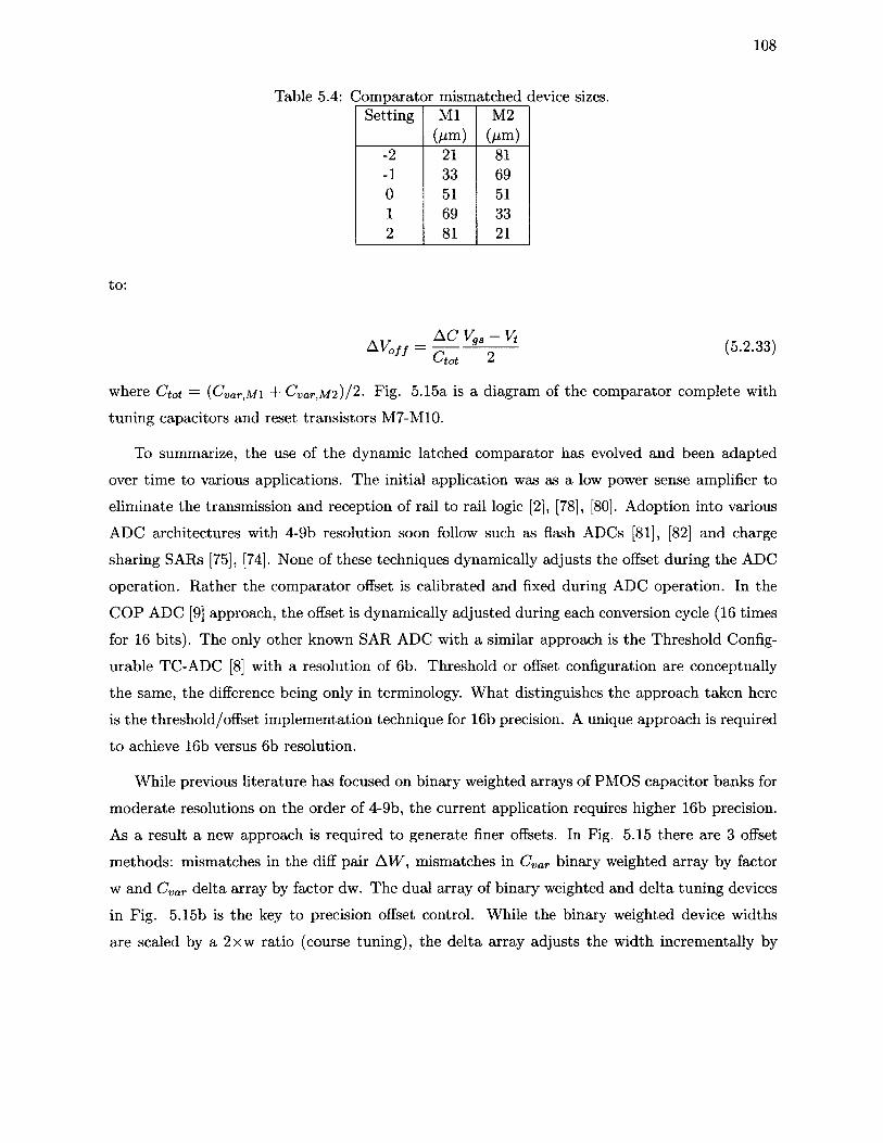
108
Table 5.4: Comparator mismatched device sizes.Setting M l
(Mm)M2
(Mm)-2 21 81-1 33 690 51 511 69 332 81 21
to:
W o f f = (5-2.33)^tot *
where Ctot — {C var,Ml + C var,M2 ) /%. Fig. 5.15a is a diagram of the comparator complete with
tuning capacitors and reset transistors M7-M10.
To summarize, the use of the dynamic latched comparator has evolved and been adapted
over time to various applications. The initial application was as a low power sense amplifier to
eliminate the transmission and reception of rail to rail logic [2], [78], [80]. Adoption into various
ADC architectures with 4-9b resolution soon follow such as flash ADCs [81], [82] and charge
sharing SARs [75], [74], None of these techniques dynamically adjusts the offset during the ADC
operation. Rather the comparator offset is calibrated and fixed during ADC operation. In the
COP ADC [9] approach, the offset is dynamically adjusted during each conversion cycle (16 times
for 16 bits). The only other known SAR ADC with a similar approach is the Threshold Config
urable TC-ADC [8] with a resolution of 6b. Threshold or offset configuration are conceptually
the same, the difference being only in terminology. W hat distinguishes the approach taken here
is the threshold/offset implementation technique for 16b precision. A unique approach is required
to achieve 16b versus 6b resolution.
While previous literature has focused on binary weighted arrays of PMOS capacitor banks for
moderate resolutions on the order of 4-9b, the current application requires higher 16b precision.
As a result a new approach is required to generate finer offsets. In Fig. 5.15 there are 3 offset
methods: mismatches in the diff pair AW , mismatches in C var binary weighted array by factor
w and Cvar delta array by factor dw. The dual array of binary weighted and delta tuning devices
in Fig. 5.15b is the key to precision offset control. While the binary weighted device widths
are scaled by a 2xw ratio (course tuning), the delta array adjusts the width incrementally by

109
elke lkM 4 M6
M7 M8 M9 M10
M3 M5
i f C/ varvarM2Ml
.AW
e lkM il
(a) Comparator core
C o u rse tu n in g
w 2w 4w 8w 16w
F in e tu n in g
a -
w -1 5 d w w-dw
- a a a -—p — -- — •■a
w+dw w + 1 5 d w
(b) Variable capacitor tuning Cvar
Figure 5.15: Comparator with variable offset threshold; a) Comparator schematic, b) Capacitive offset threshold tuning.

1 1 0
dw (fine tuning). The capacitance loading is set as follows. When zero volts is applied to the
gate the device is active and the intrinsic gate capacitance is added to the node. W hen Vcc is
applied, the device is off and only the extrinsic parasitic capacitance exists [83]. In this manner,
the capacitive loading and in turn the offsets can be precisely controlled.
For VCC=1.2V and the load driven differentially by two switching stages the maximum output
swing is 2.4VPP differential. Therefore, for 16b resolution the lsb value is 2 .4 /216 = 36.6/TV
differential. Calibration requires tuning of less than 1/2 LSB. To achieve this resolution requires
both course and fine tuning PMOS arrays of PMOS devices. Five binary weighted PMOS devices
yield a course tuning resolution of ±316 /xV. Fine tuning to 16 /xV resolution is obtained by
switching in one of the fine tuning caps with w=5 /im, L=0.5 /xm and dw=100 nm. Fig. 5.16
is a plot of the input referred offset for four course (binary weighted) and fine adjustments
(dw=100nm). This data was generated based on a schematic simulation which does not take
into account parasitics associated with layout extraction. The digital circuitry setting the gate
voltages on PMOS devices was modelled in verilogA code rather than actual gates.
The comparator power consumption was simulated while being clocked at 50 MHz. The
transient current was integrated and averaged over time to determine the average power. The
peak current is approximately 5.2mA but only for a very short time as the regenerative time
constant is < lns. As a result the average current turns out to be 100 /xA or 120 ^xW. The
comparator power is an order of magnitude less than the preamplifier.
Comparator N oise
The comparator noise performance is a limiting factor in the ADC design. For high resolution
applications a preamplifier is required to reduce the input referred noise at the expense of in
creased power consumption. An analytical model of the thermal noise [79] provides insight to
the design process. While the analysis provides guidance to the designer, ultimately the final
design remains largely an iterative procedure since factors such as device mismatch and flicker
noise are unaccounted for. Hence, optimization of noise performance remains largely an iterative
and tedious design procedure.
The comparator was simulated with Cadence PSS/Pnoise with a 1 MHz input tone and 25 or
50 MHz clock with 300 harmonics of the 1 MHz beat frequency. The total noise was calculated
by numerical integration of the input referred noise from lk to 12.5 or 25 MHz. The simulation
results are plotted in Fig. 5.17 where the noise is reduced from 72 to 57 /xVrms when the sampling

I l l
COMPARATOR CUTSET THRESHOLD P MOS TUNING
' . 4 0 m " ' 1 r ^ ! • * 4"":**
1 . 2 0 m . ^ ......■
1 . 0 0 m . '•3-—..... ....................__... -V-....
S 0 0 u L ^
6 0 0 u _ .............. ......
4 0 0 u . iV...................■*'................................................................................... _ ................... ~
2 0 0 u L _ ................— -.................—• ...........
0 . 0 0 . *'
*.....2 0 0 j r , , , , t . i . i ................................. ....
- 2 0 - 1 0 0 . 0 10 2 0 FINE TUNING ( dw)
Figure 5.16: Example of combined course and fine PMOS comparator offset tuning simulation (Course is swept from 0 to 4w, fine is -15dw to + 15dw.
is reduced from 50 to 25 MHz. When preceded by a preamplifier the cascaded input referred noise
is reduced by the amplifier voltage gain.
5.3 Cascaded Performance
The ADC design goal of 16b resolution a t a sample rate of 2.82 MHz with approximately 5mW
power constraint is very aggressive. The proposed preamp and latched comparator architecture
held promise of possible solution however, significant limiting factors were encountered during the
design process. Factors such as limited tuning range, degraded noise rejection due to mismatches
and the need for increased power to reduce noise.
5.3 .1 T uning R ange
The functional input voltage range is the tuning range. The tuning range Vtune and number of
bits n set the lsb according to Vtune/2n- For a specified resolution of n bits, Vtune and the lsb
are linearly related. Increasing Vtune relaxes the noise specification which is a fraction of a lsb.
Therefore, it is desirable to maximize Vtune to the fullest extent possible.

1 1 2
Comparator integrated noise
50MHz25MHz
>"
■o
Q.
0.5Comparator diff pair setting
Figure 5.17: Integrated input referred comparator noise.
Vtune is determined by superposition of offsets using the methods explained perviously. The
maximum Vtune is limited by two practical design constraints. Firstly, increased mismatches
leads to degraded CMRR, CDRR and DCRR parameters. This implies an inherent increase in
susceptibility to external noise sources. Secondly, very large mismatches can lead to device sizes
which are not feasible nor practical.
The input referred offset can be tuned to 16 pV resolution for an input of 280mV peak to
peak differential. This is accomplished by superposition of the preamp, comparator differential
input pair, binary weighted and delta tuning cap offsets. This yields 14.5b of resolution.
5.3 .2 C ascaded N o ise
The noise performance of the preamp and comparator have been characterized individually, there
fore the next step is to determine the cascaded performance. The cascaded input referred noise
can be calculated from the individual noise contributors. Consider Fig. 5.18 where G is the differ
ential mode voltage gain of the preamplifier, vfUp and vfUc are the integrated input referred noise
of the preamplifier and comparator respectively. The total input referred noise can be calculated
from each contributor [84] as,

where V{n to t is the RMS input referred noise voltage. The simulated cascaded noise plots for both
sample rates are shown in Fig. 5.19. The noise was numerically integrated up to half the sample
rate with no comparator mismatch.
At the onset, the design goal was to achieve an input referred noise which is a fraction of a
lsb. The noise should be on the order of 1/2 to l/61sb. The former tending to be error prone
and the latter requiring significant power increase. Assuming a full swing of 2.4Vpp the lsb is
36.6 /xV so the input referred noise should be in the range of 6.1 to 18.3 /zV. The initial design
did not anticipate the increased noise due to mismatch nor limited tuning range, thus in Fig.
5.19 for 50 MHz and pream p=0 the noise 14.5 /zV result was deemed acceptable. Subsequently,
increased noise due to mismatch and limited tuning range effectively required re-design to reduce
the system noise further. Due to time constraints in the fabrication schedule, the decision was
made to proceed with the current design.
A potentially significant noise reduction is possible with a comparator modification. The ther
mal noise contribution of some of the devices, including M l and M2 in Fig. 5.15 are proportional
to k T jC x [79]. Cx is the to tal capacitance on the drain nodes of M l or M2 determined from
Cx = Cvar + Cp where Cp includes the layout and device parasitic capacitances. Thus, adding
extra capacitance Cextra to Cx will reduce the noise. The tradeoff in doing so is to slow down
the discharge or slewing rate during the comparison mode and also an increase in power. In Fig.
5.20 the cascaded noise reduction for Cextra=2pF yields a relative noise reduction of 5.5 /xV and
current increase of 240/xA. Even with the extra 2pF loading the comparator decision is made well
within the 10 ns window. Increasing Cextra above 2 pF yields diminishing returns. Note tha t
changing the loading on Cx requires redesign of PMOS arrays comprising Cvar- In addition, the
time the RC time constant during reset will increase. As with the preamplifier the comparator
could also be implemented in PMOS to reduce 1 /f noise.
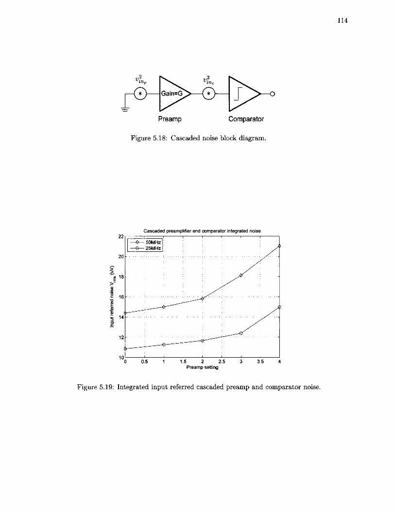
114
I- © "Gain=G
Preamp Comparator
Figure 5.18: Cascaded noise block diagram.
Cascaded preamplifier and comparator integrated noise
-0— 50MHz 25MHz
20
(0>4)</>oc73i=&a>3Q .C
0.5 2.5 3.5Preamp setting
Figure 5.19: Integrated input referred cascaded preamp and comparator noise.
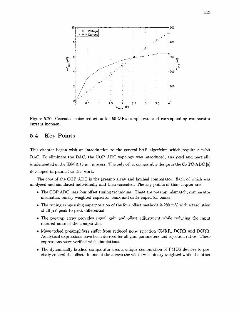
115
500-*— Voltage €» - Current
400
300>aE
200
100
0 .5 2.5 3 .5C „ < pF ) extra '
Figure 5.20: Cascaded noise reduction for 50 MHz sample rate and corresponding comparator current increase.
5.4 K ey Points
This chapter began with an introduction to the general SAR algorithm which require a n-bit
DAC. To eliminate the DAC, the COP ADC topology was introduced, analyzed and partially
implemented in the IBM 0.13 jum process. The only other comparable design is the 6b TC-ADC [8]
developed in parallel to this work.
The core of the COP ADC is the preamp array and latched comparator. Each of which was analyzed and simulated individually and then cascaded. The key points of this chapter are:
• The COP ADC uses four offset tuning techniques. These are preamp mismatch, comparator mismatch, binary weighted capacitor bank and delta capacitor banks.
• The tuning range using superposition of the four offset methods is 280 mV with a resolution of 16 /iV peak to peak differential.
• The preamp array provides signal gain and offset adjustment while reducing the input referred noise of the comparator.
• Mismatched preamplifiers suffer from reduced noise rejection CMRR, DCRR and DCRR. Analytical expressions have been derived for all gain param eters and rejection ratios. These expressions were verified with simulations.
• The dynamically latched comparator uses a unique combination of PMOS devices to precisely control the offset. In one of the arrays the width w is binary weighted while the other

116
array introduces a delta change w+dw.
• For lower 1 /f noise the preamp and comparator should be designed with PMOS transistors.
• for low frequency operation the resolution is 280mV/16pV=17,500 or 14.1b. The worst case noise performance is 21pV from Fig. 5.19. Assuming a noise allowance of l/21sb the resolution at 50MHx would be 280mV/42pV=19,048 or 12.7b.
• At the expense of a slight increase in power, an extra fixed capacitive load Ceitra=2pF will reduce the cascaded noise by 5 /iV. The binary and delta weighted capacitive arrays would have to be redesigned in this case.
Chapter 6
A D C Test and M easurem ents
Custom hardware and software for an autom ated measurement platform was developed for testing
the COP ADC. Two platforms were developed for both DC and AC characterization. Offset
measurements are presented and compared to simulation results. Due to hysteresis and noise
limitations a fully functional ADC could not be tested.
The chapter concludes with a comparison table of recently published digital input Class D
amplifiers and a list of key points.
6.1 Integrated Circuit Overview
The Integrated Circuit (IC) block diagram with pinout is shown in Fig. 6.1. The IC was fabricated
in the IBM CMRF8SF 0.13 /zm CMOS process and wire bonded in a CFP-24 surface mount
package. The analog and digital sections have separate supplies and corresponding ground pins.
Test points provide both input and output access to the internal nodes between the preamplifiers
and comparator. These pins are controlled by active high logic applied to the control pins 14 and
15. The TPO UT pins are buffered internally with a pair of source followers capable of driving
50 loads with minimal attenuation. The TPIN pins are connected to the internal nodes via
transmission gates. Table 6.1 includes a list of the pins with brief descriptions.
6.2 D igital Interface
The PC digital interface consists of six data pins D(5:0), three clock pins (CLK_COMP, CLK_REG
and CLK.DATA) and two active high enable pins (ENTP_OUT and ENTP_OUT) for the test
117

118
T P TP T P TP ENABLE ENABLEAGND VCCA OUT_ N OUT_P IN _N IN_P T P J N TP_O U T
ANALOG
OUT PVIN PPREAMPARRAY FLIP
FLOPCOMPARATOR
OUT N
BIASBIASCL KCO M P
FET C A P S
DIGITAL I/O
PREAMPDECODE
DELTA WCOMP
24b Config Register CR(23:0)DELAY
6 x 4b Shift Register
CL K DGND D(5) D<4) D(3) D(2) D (l) D(0) VCCDCL K CLKCOM P REG DATA
Figure 6.1: Integrated circuit block diagram and pinout.
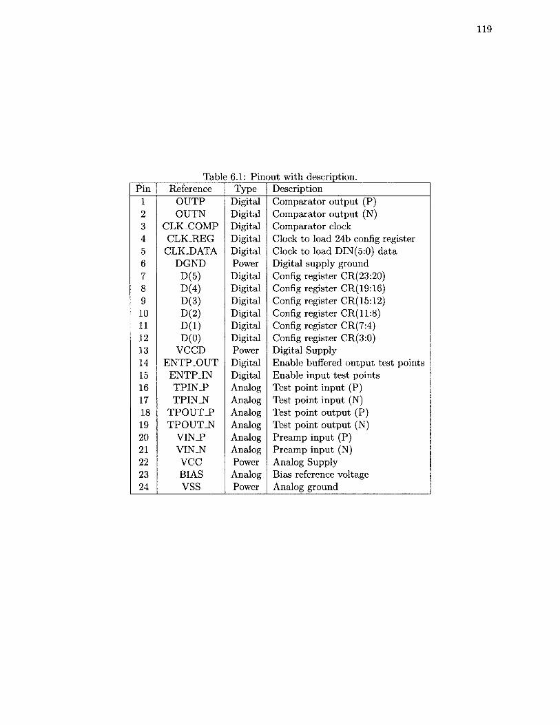
Table 6.1: Pinout with description.Pin Reference Type Description
1 OUTP Digital Comparator output (P)2 OUTN Digital Comparator output (N)3 CLK_COMP Digital Comparator clock4 CLKJREG Digital Clock to load 24b config register5 CLK.DATA Digital Clock to load DIN(5:0) data6 DGND Power Digital supply ground7 D(5) Digital Config register CR(23:20)8 D(4) Digital Config register CR(19:16)9 D(3) Digital Config register CR(15:12)10 D(2) Digital Config register CR(11:8)11 D (l) Digital Config register CR(7:4)12 D(0) Digital Config register CR(3:0)13 VCCD Power Digital Supply14 EN TP.O U T Digital Enable buffered output test points15 E N T P JN Digital Enable input test points16 TPINJP Analog Test point input (P)17 TPINJNT Analog Test point input (N)18 TPOUT_P Analog Test point output (P)19 TPOUTJSf Analog Test point output (N)20 VINJP Analog Pream p input (P)21 VIN_N Analog Preamp input (N)22 v c c Power Analog Supply23 BIAS Analog Bias reference voltage24 v s s Power Analog ground

1 2 0
Table 6.2: Config register settings for programmable offsets.Parameter Register No. of settings Decimal SettingsPreamplifier select CR(23:20) 9 1 to 9Comparator Diff Pair select CR(19:15) 5 1,2,4,8,16Comparator binary weighted PFETs (neg) CR(14:10) 32 0 to 31Comparator binary weighted PFETs (pos) CR(9:5) 32 0 to 31Comparator Delta PFETs CR(4:0) 32 0 to 31
CLK REF
C L K D A T A I
C L K R E G _____ |
CLK CO M P
O U T_P ---------O U T_ N ______
■ * « > ~ r i i » tFigure 6.2: Digital interface timing diagram.
points. All digital circuitry operates on an independent 1.2V DC supply.
The four different offset options are configured with a 24b register CR(23:0). Table 6.2 lists
the parameters and associated control bits. The data must be parsed into into 6 nibbles for
loading on the data pins D(5:0). This reduces the clock frequency by a factor of six compared to
loading the data in a serial manner.
The data is loaded according to the timing diagram of Fig. 6.2. All clock signals are derived
from the master clock, CLK-REF. W ith 6 data lines D(5:0), 24 bits are clocked in after the
fourth falling edges of CLKJDATA. Subsequently, the config register is loaded on the falling edge
of CLKJRJEG. At this point the IC is ready for comparator operation, upon assertion of the
following CLKLCOMP pulse.

1 2 1
6.3 M easurement System
There are two fully automated DC and AC measurement systems. Each system is explained in
this section along with measurement results. In addition, the custom designed two layer FR4 test
PCB with 2oz copper and thickness of 0.062 inches is described.
6 .3 .1 P rin ted C ircuit B oard
Testing was facilitated by way of a custom designed two layer Printed Circuit Board (PCB)
shown in Fig. 6.3. The PCB schematic and layout are included in Appendix B. The PCB has
the following features.
• Separate analog and digital power supplies and ground planes
• Buffered 1.2V to 3.3V level shifters for comparator OUTP,N (pins 1,2)
• Differential to single ended low noise opamp circuit for TPOUT_P,N (pins 18,19)
• Single ended balun or differential input to TPINJP,N (pins 16,17)
• Header jumpers for EN TP.O U T and E N T P JN enable (pins 14,15).
• Multiple VIN_P,N (pins 20,21) connection options including, differential, single ended with balun and single ended with balun and sample and hold.
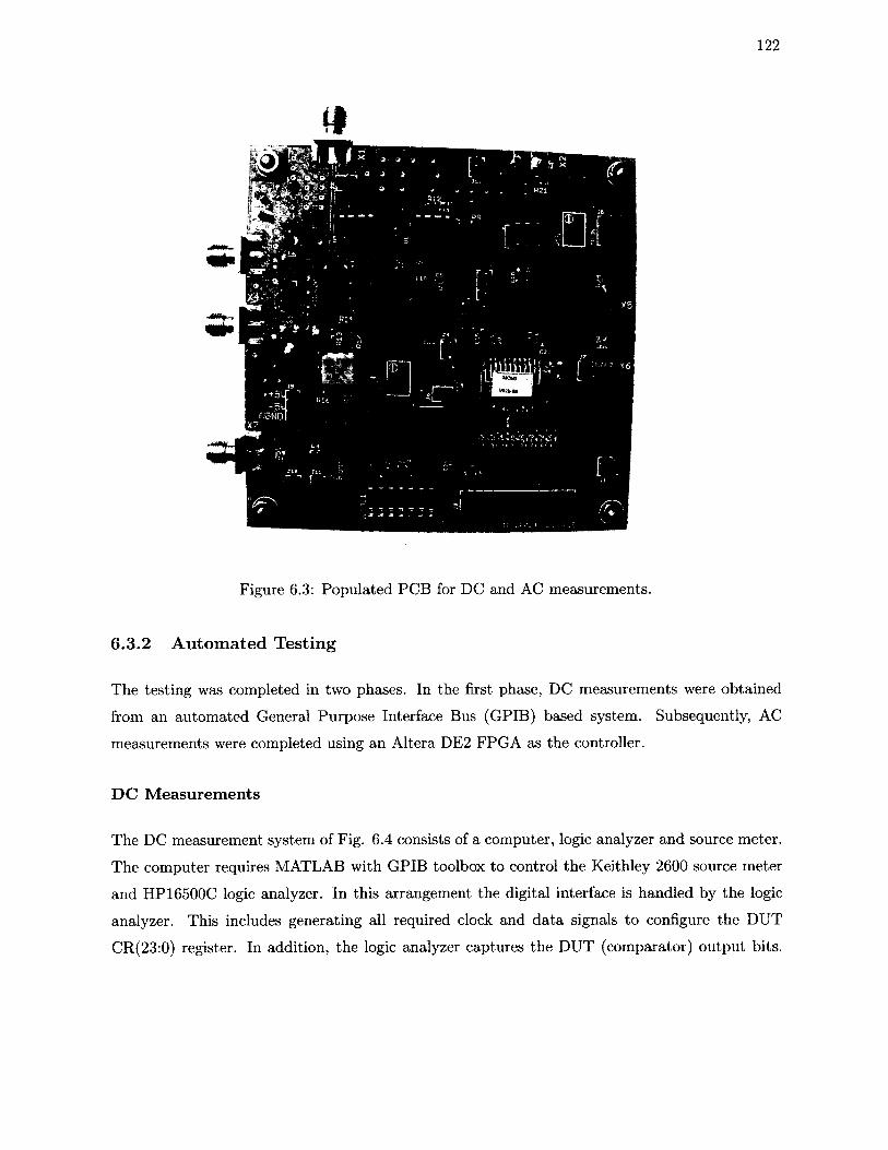
Figure 6.3: Populated PCB for DC and AC measurements.
6 .3 .2 A u to m a ted T estin g
The testing was completed in two phases. In the first phase, DC measurements were obtained
from an autom ated General Purpose Interface Bus (GPIB) based system. Subsequently, AC
measurements were completed using an Altera DE2 FPGA as the controller.
DC M easurements
The DC measurement system of Fig. 6.4 consists of a computer, logic analyzer and source meter.
The computer requires MATLAB with GPIB toolbox to control the Keithley 2600 source meter
and HP16500C logic analyzer. In this arrangement the digital interface is handled by the logic
analyzer. This includes generating all required clock and data signals to configure the DUT
CR(23:0) register. In addition, the logic analyzer captures the DUT (comparator) output bits.
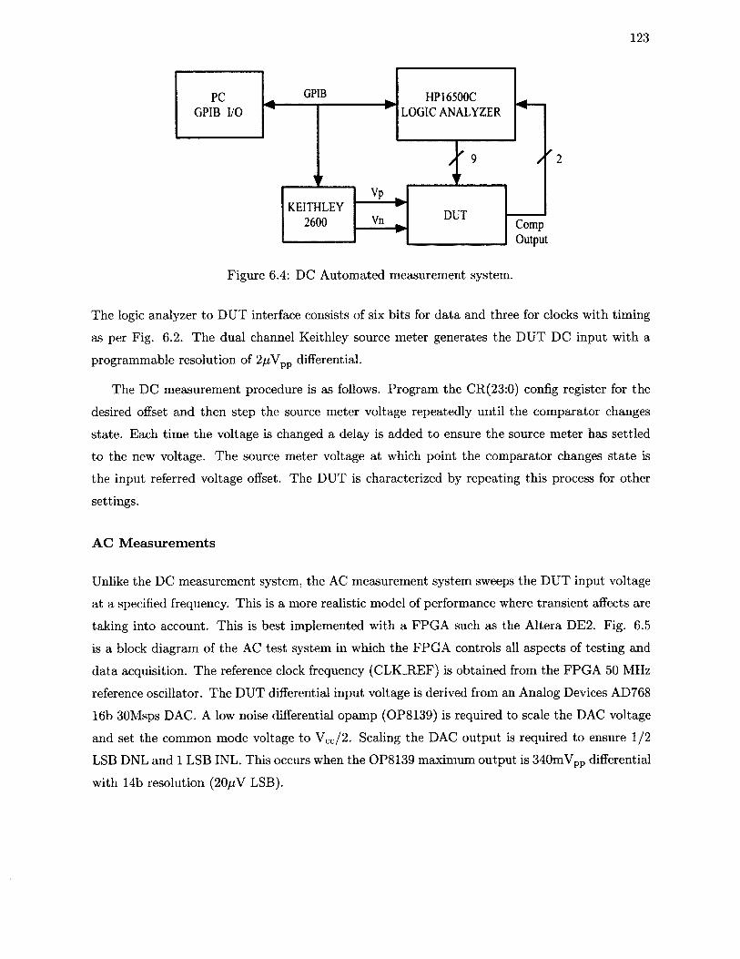
123
GPIB
Vn CompOutput
KEITHLEY2600
PC GPIB I/O
DUT
HP16500C LOGIC ANALYZER
Figure 6.4: DC Automated measurement system.
The logic analyzer to DUT interface consists of six bits for data and three for clocks with timing
as per Fig. 6.2. The dual channel Keithley source meter generates the DUT DC input w ith a
programmable resolution of 2pVpp differential.
The DC measurement procedure is as follows. Program the CR(23:0) config register for the
desired offset and then step the source meter voltage repeatedly until the comparator changes
state. Each time the voltage is changed a delay is added to ensure the source meter has settled
to the new voltage. The source meter voltage at which point the comparator changes state is
the input referred voltage offset. The DUT is characterized by repeating this process for other
settings.
AC M easurements
Unlike the DC measurement system, the AC measurement system sweeps the DUT input voltage
at a specified frequency. This is a more realistic model of performance where transient affects are
taking into account. This is best implemented with a FPGA such as the Altera DE2. Fig. 6.5
is a block diagram of the AC test system in which the FPGA controls all aspects of testing and
data acquisition. The reference clock frequency (CLK_REF) is obtained from the FPGA 50 MHz
reference oscillator. The DUT differential input voltage is derived from an Analog Devices AD768
16b 30Msps DAC. A low noise differential opamp (OP8139) is required to scale the DAC voltage
and set the common mode voltage to Vcc/2. Scaling the DAC output is required to ensure 1/2
LSB DNL and 1 LSB INL. This occurs when the OP8139 maximum output is 340mVpp differential
with 14b resolution (20/xV LSB).

124
CLK _ DAC DAC (15:0)
O P8139DAC768 Vn
C L K (2:0 ), D (5:0)
CO M P Q U T(1:0)
DUTAltera DE2
FPGA
Figure 6.5: AC Automated measurement system.
6.4 M easurem ent Results
The measurement results for both the DC and AC test setups will be presented. In the DC
measurements each family of offsets is measured independently. The data is then numerically
superimposed to determine the overall tuning range and resolution. The superposition principle
is verified in the AC measurements where all offset combinations can be measured directly. The
AC measurements also account for transient effects.
6 .4 .1 D C M easu rem en ts
W ith the measurement system of Fig. 6.4 the offsets were measured for each of the four offset
configurations. W ith GPIB controlled instrum ents delays are introduced to allow for instrument
settling time. The logic analyzer is configured with a CLK_REF of 50 MHz from which all clock
and data waveforms are synchronized. The measured and simulated (layout extracted) offsets are
presented in Figs. 6.6a-d. The non-linearity in Figs. 6.6a,b is due to the on-chip interconnect
and Ron impedance of the digital control devices. This problem can be corrected by inserting
an appropriately sized pair of inverter buffers (one in the digital section and one in the analog
section) to provide a low impedance ground at the gates of the PMOS devices.
The binary weighted data of Fig. 6.6b can be shifted up or down to create a family of traces.
This is possible since there is independent control of the PMOS positive and negative arrays as
per registers CR(14:10) and CR(9:5) in Table 6.2. This is not possible for the delta case since
the arrays share common control lines.
Table 6.3 was calculated by curve fitting the measurements to a linear first order polynomial.

125
Table 6.3: DC Measured input referrec offset reso ution and tuning range.Offset Resolution RMSe No. Steps RangeParameter pk-pk diff (V)Delta caps 15.5uV 4.96 fiV ±15 ±232.5uVBinary weighted caps 316uV 131.5pV ±15 ±4.74mVComparator diff pair 7.9mV 2.14mV ±2 ±15.8mVPreamp diff pair 29.85mV 3.07mV ±4 ±119.4mV
The RMS error between the measured and simulated data is calculated from,
1 nR M S e = - ^ ( V ^ i - VOS}i)2 (6.4.1)
\ n i = i
where Vom and Vos are the measured and simulated offsets, respectively.
The overall tuning range is obtained by superposition of the offset families. Sufficient overlap
of the various tuning ranges is required to to avoid missing codes. Strictly speaking, linear
superposition of the offsets is an approximation due to slight gain variation across the preamplifier
array. Complete characterization of the offsets is best suited to AC measurements. Simulations
confirm tha t the offset variation is directly proportional to the gain variation in the preamp
array. For mismatched preamps the gain is reduced according to Fig. 5.8a and as a result, the
comparator input referred offset will increase proportionally.
The calculated tuning range based on the DC measurements is 282.6 mV. The resolution with
no missing codes is 17.1uV which equates to 14b. The INL and DNL plots are given in Fig. 6.7.
To achieve the required 16b operation two improvements in the design are required. First, the
tuning range needs to be increased and secondly, the cascaded noise needs to be reduced. These
two changes pose significant risk and challenge. Increasing the tuning range requires extending
the mismatch in the preamp and comparator. This will inevitably lead to an undesirable increase
in A d m - c m and A c m -.d m - Noise reduction comes at the expense of increased power consumption.
H ysteresis
While doing manual characterization and DC measurements hysteresis was observed. T hat is,
the comparator exhibits a tendency to remain in its past state. Hysteresis is a memory effect
th a t is usually associated with capacitor charge retention and/or feedback. This affect was not

126
a) Delta weighted PMOS caps b) Binary weighted PMOS caps300
SimulatedMeasured
200
100>3®itO
-100
-200
-300-20 -10
Digital setting
SimulatedMeasured
>E®
£o
-10Digital setting
c) Comparator diff pair mismatch d) Preamp diff pair mismatch
SimulatedMeasured
>E®
i tO -5
-10
-1 5
-20
Digital setting
150SimulatedMeasured
100
>E®
£o-5 0
-100
-15 0-4 2 0 2 4
Digital setting
Figure 6.6: Measured and extracted layout offset simulations. Voltages are input referred peak to peak differential.

DNL
(LSB
) INL
(L
SB)
127
0.5
0.25
0
-0.25
-0.5 0.5
0.25
0
-0.25
-0.5-10 -5 0 5 10
LSBs (x103)
Figure 6.7: INL and DNL plots normalized to LSB (LSB=17.1/iV) based on superposition of DC measurements.

128
foreseen during the design phase since the comparator has a reset phase in which all relevant
internal capacitances (offset capacitor arrays and positive feedback inverters) are pre-charged.
Schematic simulations indicate no discernable hysteresis however, extracted layout simulations
show approximately 50-75/rV. This amount is significantly less then measurements.
One possible cause of hysteresis in latched type comparators is due to the data dependent
loading of the flip flop connected to the output of the comparator [80]. It is proposed that
buffering the output of the comparator would result in virtually no hysteresis effect though this
was not experimentally proven.
The hysteresis in [80] was in the range of 3-7mV while measurements for this design are on
the order of l-2mV. To date, hysteresis has not been an issue for latched comparators since it
is less than the resolution of interest. For example, for a 6b ADC with programmable latched
comparator the LSB is 5mV [8], therefore hysteresis is of little consequence. For 14-16b resolution
and LSBs on the order of microvolts it becomes a fundamental limitation.
Its possible tha t some feedback associated with the PCB is contributing to the hysteresis
though this remains to be verified. One way to mitigate the hysteresis is to double the number
of comparator operations. For a n-bit SAR there is usually n samples. If instead, there are
2n samples and every 2nd sample is used to clear the hysteresis. This can be accomplished by
enabling the appropriate preamp to produce a DC offset tha t will clear the comparator hysteresis.
Though technically feasible, it is a undesirable approach due to increased power consumption.
6 .4 .2 A C M easurem en ts
The DAC AD768 and opamp OP8139 are configured for 14b operation over a range of 340mVpp
differential equating to a resolution of 20.75pVpp. The FPGA generates all timing waveforms and
steps the DAC register in a linear fashion, generating a triangular waveform. For each period of
the triangular waveform the DUT configuration register is fixed. Thus, the DUT offset is obtained
directly from the DAC register a t the comparator tripping point. The DAC register is stored in
the FPGA SRAM for post processing. Measured waveforms for the DAC (triangular) and DUT
(square wave) differential outputs are given in Fig. 6.8. Considering all register settings there
are 1,474,560 possible combinations.
The FPGA timing is based on CLK_REF derived from the onboard 50 MHz oscillator. It is
divided by eight to produce a CLK_REG frequency of 6.25 MHz which is the sample rate. Note

129
Tek a w n 250ks/s 149 Acqs[ - ------------------------------T —
C3 Freq 312.505 Hz Low signal amplitude
Figure 6.8: AC test waveforms including differential DAC and comparator output.
th a t CLK_REG and CLK_DAC are essentially the same where CLK_DAC is the clock for loading
the DAC register.
After measuring the offsets the FPGA SRAM data is post processed in Matlab to determine
the tuning range and resolution. The INL and DNL plots calculated from the measured data
are plotted in Fig. 6.9. The maximum INL is 0.5 LSB and DNL 1 LSB. The tuning range was
293.33mVpp differential with 14b resolution (LSB=20.75//V).
Table 6.4 summarizes the results for cycling the DUT through all offset combinations. The
overall tuning range of 293.33 mVpp differential is 3.8% greater then the DC tuning range of
282.6mVpp with assumed superposition. This difference can partially be attributed to calibration
and measurement error in the opamp gain. The AC results are im portant for two reasons. First,
the superposition assumption of DC measurements is verified. Secondly, dynamic measurements
a t a sample rate of 6.25 MHz take into account transient affects though only a t 1/8 the intended
rate. For these test results we can calculate the ADC figure of merit as,
V I 1 2 x 10⁻³ • 1 25F O M = u . 2H n o b = ((6.25 x 10⁶)/14) ■ 213-8 = ° '24 PJ / conversion- <6-4-2>
Offset superposition is critical with respect to automated testing in a commercial production
environment. In this case, the goal would be to characterize the device using only a subset of
200mV M2.00ms Ch3 I5.00 VCh3 5.00 V
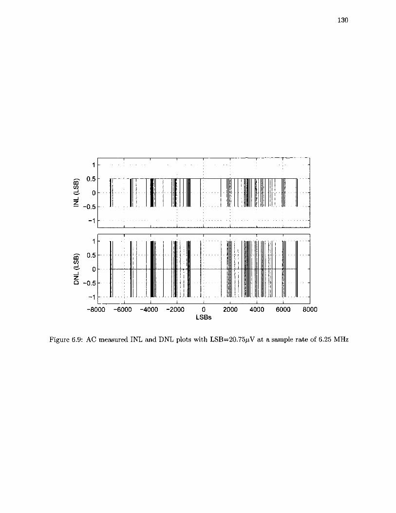
DNL
(LSB
) INL
(L
SB)
130
1
0.5
0
-0.5
-1
0.5
-0.5
-8000 -6000 -4000 -2000 0 2000 4000 6000 8000LSBs
Figure 6.9: AC measured INL and DNL plots with LSB=20.75/iV at a sample rate of 6.25 MHz
04344^

131
Table 6.4: Measured input referred offset resolution and tuning range.State Range LSB No. of bits Missing Max INL Max DNL
(mVpp) (uV) Codes (LSBs) (LSBs)DC 282.60 17.09 14.0 0 0.38 0.41AC 293.33 20.75 13.8 0 0.50 1.00
measurements to reduce verification time. W hether or not this is practically feasible requires
further analysis to determine total process and corner variation. Its possible further circuitry
dedicated to calibration is necessary.
Using the AC measurement data an inferred SNR can be calculated for a sine input of 222.5
Hz, calculated from the 6.25 MHz frequency, resolution and maximum input amplitude. The
calculated SNR was 84dB (14b) where the noise was integrated from DC to f sj 2 = 3.125 MHz.
N oise
The comparator input RMS noise determines the confidence level for reliable offset measurement.
A noisy differential comparator is shown in Fig. 6.10. The digital output for a given input can
be modelled as,
v0 = sign(Uo2 -V o i) =1 + sign(vdin - vn)
(6.4.3)
where Vdin = Vn — U;2 and vn is the input noise voltage [79]. If the argument of the sign function
is positive the output is 1 (Vcc) whereas it is 0 (—Vcc) for a negative argument. This model
neglects any memory or hysteresis effects due to parasitic feedback in the IC or PCB. Assuming
vn is modelled as zero mean white Gaussian noise, then the probability of a high output as
a function of Vdin corresponds to the comparator output mean (expected value) and can be
calculated as,
P (V din)V2tti7T(7r
+oo
J v° e x p l -7 ^ 21+erf(7fe) (6.4.4)
where
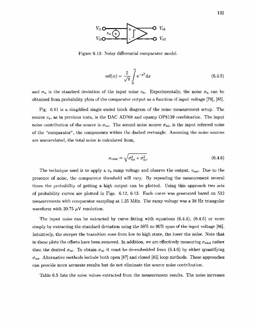
132
Vn Oi
V i2C h
■o v ol
- O Vo2
Figure 6.10: Noisy differential comparator model.
erf(a)
a
/■ (6.4.5)
and an is the standard deviation of the input noise vn . Experimentally, the noise an can be
obtained from probability plots of the comparator output as a function of input voltage [79], [85].
Fig. 6.11 is a simplified single ended block diagram of the noise measurement setup. The
source vs, as in previous tests, is the DAC AD768 and opamp OP8139 combination. The input
noise contribution of the source is ans. The second noise source ani. is the input referred noise
of the “comparator” , the components within the dashed rectangle. Assuming the noise sources
are uncorrelated, the total noise is calculated from,
vntot = (6-4-6)
The technique used is to apply a vs ramp voltage and observe the output, v ^ t- Due to the
presence of noise, the comparator threshold will vary. By repeating the measurement several
times the probability of getting a high output can be plotted. Using this approach two sets
of probability curves are plotted in Figs. 6.12, 6.13. Each curve was generated based on 512
measurements with comparator sampling at 1.25 MHz. The ramp voltage was a 38 Hz triangular
waveform with 20.75 pV resolution.
The input noise can be extracted by curve fitting with equations (6.4.4), (6.4.5) or more
simply by extracting the standard deviation using the 50% to 90% span of the input voltage [86].
Intuitively, the steeper the transition zone from low to high state, the lower the noise. Note that
in these plots the offsets have been removed. In addition, we are effectively measuring <Jntot rather
then the desired ani- To obtain ani it must be de-embedded from (6.4.6) by either quantifying
ans. Alternative methods include both open [87] and closed [85] loop methods. These approaches
can provide more accurate results but do not eliminate the source noise contribution.
Table 6.5 lists the noise values extracted from the measurement results. The noise increases

133
Table 6.5: Noise measurements.State Input Noise antot
(/xVrms)PreampO 89.9Pream pl 79.8Preamp2 84.8Preamp3 92.4Preamp4 107.7CDPO 88.2CDP1 100.9CDP2 119.9
ns
ComparatorPreamp
Figure 6.11: Input noise associated with the source and cascaded preamp and comparator.
with increasing device mismatch. This is to be expected given the simulation results presented
in Chapter 5. In addition, when mismatch is introduced to generate an offset the CMRR, DCRR
and CDRR parameters are degraded. Therefore, source noise is more likely to affect performance.
There is an anomaly in tha t PreampO noise values are higher then th a t of Pream pl,2. This could
be due to measurement error and would require re-testing to confirm.
Some test system modifications to reduce the source noise include,
• Repeating the measurement using the Keithley source meter and GPIB control.
• Replacing the DAC AD768 with a lower noise, higher resolution DAC.
• Reconfiguring the measurement system for closed loop operation [85].

134
Preamplifier1
- — PreampO -*— Preampl - e — Preamp2 -0— Preamp3 -v— Preamp4
0.9
0.8
3 0.7
0.6
0.5
S 0.4
cl 0.3
0.2
0.1
O1 O1 ~n ------ ‘—-400 -300 -200 -100 0 100 200 300 400
Input (pV)
Figure 6.12: Measured probability of a high output as a function of input voltage for different preamp settings.
Comparator Differential Pair
-s— CDP2 -*— CDP1 - — CDP0
0.9
0.8
3 0.7
0.6
0.5
S 0.4
o- 0.3
0.2
0.1
-200 -100 100-300 200 300Input (pV)
Figure 6.13: Measured probability of a high output as a function of input voltage for different comparator diff pair settings.
135
6.5 Comparison Table
Table 6.6 is a summary of recent publications related to digital input Category III-V Class D
amplifiers. Analog input Category I-II Class D amplifiers are not included as they require an ex
ternal DAC for a complete solution. The reader is referred to [39,55] for analog input comparison
tables. All power consumption values are for single channel operation. The performance values
for the parameters are explained in the following sections.
Most of the listed publications are for higher power applications (>400 mW) such as hands
free speakers in handsets or tablet/lap top speakers. In these cases the overall efficiency is better
than lower output applications. This can partly be attributed to the overhead associated with
the quiescent power.
6.5 .1 Q uiescen t Pow er E stim ate
The to tal power consumption of the system will include switching losses of the power stage, COP
ADC and digital circuitry. The digital circuitry power consumption can be estimated from,
Pd = \ f C t V l (6.5.1)
where / is the clock frequency, Ct is the total capacitance and it is assumed tha t on average 50%
of the gates are active. Ct can be estimated by first obtaining the equivalent number two input
nand gates for each digital circuit and multiplying by the input capacitance. For the interpolation
filters, loop filter, DPW M and clock divider circuits Pd — 52/xW.
During normal operation the Class D PA will incur both switching and conduction losses. In
the quiescent case it is assumed tha t there is no load or zero output power. In this case there are
switching but no conduction losses.
For a differential bridge tied load configuration as given in Sec. 4.5.3 the switching losses are
2x77 = 154/iW. The core of the COP ADC consisting of the preamp and comparator dissipates
1.5 mW of power. The estimated quiescent power per channel is 1.706 mW.

Table 6.6: Published specifications for digital input Class D audio amplifiers. All power specifications are for single channel mono operation._______________________________________________________________________________ __________ _________________
Parameter [49] [50] [51] [53] [57] [31] [55] [88]Linear
[89] [6]Thiswork
Category I-V III III III IV IV IV IV IV IV V VAnalog (V) 2.5 3.0 5.0 5.0 4.8 5.0 5.0 5.0 1.8 25 1.2Digital (V) 1.2 1.2 1.2 5.0 1.2 1.8 1.8 1.8 1.8 FPGA 1.2Max POUT (mW) 12.5 400 1000 1000 330 1000 3400 2400 15 15000 10Max efficiency (%) 80 88 81 70 84 92 90 86 36.5 - 80.3THD+N (%) 0.1 1 0.2 0.1 - 1 10 1 0.03 0.001 -PSRR @217 Hz (dB) - - 64 90 90 80 85 85 105 - 78SNR A-weighted (dB) 103 92 104 - 93 92 - 96 91 - 84Dynamic Range (dB) 96 120 104 83 - 92 103 - - - -Quiescent Power (mW) 1.3 6.48 8.3 - - - 7.6 10.4 6.8 - 1.71Process 65nm 65nm 0.13/xm 0.5/xm 90nm 0.14/im 0.14/xm - BiCMOS PCB 0.13/xm
COOi

137
6 .5 .2 M axim um S ystem E fficiency
The maximum collector efficiency can be determined by extension of the quiescent power to
account for additional conduction losses incurred at maximum output power. Note tha t the effi
ciency to be calculated includes all system components, not just the PA efficiency as is sometimes
reported.
Applying equation (4.5.7) and assuming a bridge tied load with Ri = 3217 and R on = 1.217,
the conduction loss Pc=0.75 mW for an output power 10 mW. The switching losses have been
accounted for in the quiescent power calculations, therefore only the conduction losses need to be
added. The peak efficiency which occurs at maximum output power is r)c = 10/(1.706 +10.75) =
80.3%.
6 .5 .3 O th er P aram eters
The noise rejection a t 217 Hz is based on the sum of two values. A common mode rejection of 30
dB is assumed for the differential bridge tied load and another 48 dB from feedback (Fig. 4.14).
This is sufficient for direct battery connection in GSM handsets.
The listed SNR of 84dB is the theoretical limit for a 14b ADC and has been verified in
simulink. The dynamic range and THD+N values are not specified since a fully functional mixed
signal simulation of the entire system was not completed.
6.6 K ey Points
In this chapter the AC and DC automated test setup was presented including details of the custom
designed verification PCB. The details of the digital and analog IC interface were provided along
with a pinout table and timing diagrams.
AC measurements were completed after DC measurements with the results being well corre
lated. The AC measurements could be significantly improved with a higher resolution 18b DAC
and ideally eliminating the opamp buffer to keep noise to a minimum. Ideally the measurements
should be limited by the noise of the DUT and not the source.
Measurement results indicated hysteresis which is not accounted for in simulations. This
imposes a limitation on the COP ADC resolution in which full 14b resolution can not be obtained

138
directly. Hysteresis and source noise are two limiting factors in completely characterizing the COP
ADC.
Other key points from this chapter are:
• The DC measurement system was based on GPIB instrument control. Automated testing software was written in Matlab.
• The AC measurement system was based on an FPGA controller. A utomated testing software was written in Verilog.
• The 1x2mm die was bonded to a 24 pin surface mount package and soldered to the test PCB.
• The input voltage operating range and resolution for the AC and DC measurements were similar. Approximately 280 mV with 14b resolution and no missing codes. The AC sample rate was 6.25 MHz which is 1/8 the required frequency.
• The DC measurements measured each set of offsets and then applied superposition to predict the tuning range. The AC measurements verified this assumption by measuring all offset combinations.
• Noise measurements are higher then simulated but include noise from the source. An alternate measurement approach is required to measure the preamp and com parator noise. This can include using a lower noise/higher resolution DAC, switching to a GPIB measurement system or using a closed loop measurement system [85]. Worst case <rniot=120 pVrms.
• Noise antot increases as the degree of device mismatch increases. This is due to increased thermal noise and degraded noise rejection ratio performance.
• There was significantly more hysteresis in the measurements then simulations. Schematic simulations do not reveal hysteresis but extracted simulations show a small amount on the order of 50-75 pV.
• One way to mitigate the hysteresis is to double the number of samples in the SAR algorithm to clear the memory effect. The tradeoff being either reduced conversion speed or increased power if the clock frequency is doubled.
• Since the COP ADC was not fully functional it could not replace the commercial ADC (AD7621) in the FPGA system verification test platform.

Chapter 7
Conclusions
At the onset of this research the goal was to design a low power switching mode Class D amplifier
tha t is scalable. The system specifications were chosen to be comparable with current commercial
products. While no immediate benefits would be obtained, the architecture would have the
advantage rapid porting to new processes with minimal redesign and faster time to market.
Significant progress towards achieving the initial goals has been made though considerable
challenges remain. While a predominately digital system with global feedback was demonstrated
the ADC power consumption remains a significant obstacle. Furthermore, system analysis indi
cates tha t the shaped quantization noise associated with SA ADCs is problematic in closed loop
operation. This limits the designers options in selecting an ADC architecture.
To meet the system requirements the design of a low power ADC was undertaken which
led to the so called COP ADC. The ADC required 16b resolution at 2.82Msps and maximum
power of 5mW. The COP ADC was designed in a 0.13pm IBM process and tested on custom
designed automated platform. While the concept of the COP ADC architecture was validated, full
functionality according to specifications was not met. Limited tuning range, noise and hysteresis
are issues tha t require further research and development. Despite these limitations significant
advancement in the design and analysis of an alternate low power ADC architecture was made.
Measurement results from both the AC and DC tests were well correlated. An operating range
of 293mV with 13.8b resolution with 6.25MHz clock was achieved. The maximum INL=0.5 LSB,
DNL=1 LSB and a figure of merit of 0.24pJ/conversion.
The COP ADC design implemented various unique design concepts. In particular, the preci
sion DAC required in conventional SAR algorithm was eliminated by a series of digitally controlled
139

140
offsets. These offsets were implemented by direct device mismatch and capacitive loading tech
niques. The capacitive loads are parasitic PFE T s which exploit sub-micron transistor mismatches
to achieve precision femto-Farad capacitive tuning. This technique is used to generate offset in
the microvolt range. For larger offsets in the millivolt range differential pairs in the comparator
and preamplifiers are grossly mismatched.
Formulas for differential mode gain and rejection ratios were derived using equivalent half
mode circuit analysis to account for the effects of device mismatch. This analysis is normally
inconsequential as differential circuit design and layout are carefully optimized. The COP ADC
uses several intentional mismatch techniques to create voltage offsets. As a result, CMRR, DCRR,
and CDRR are finite and cannot be neglected. In particular, CMRR and DCRR render the
preamplifier and comparator susceptible to external noise. The formulas for a differential pair
amplifier were verified in simulations.
7.1 Future Work
The following issues tha t arose in this thesis should be studied in greater detail in future work.
1. The system prototype presented in Chapter 4 included a first order low pass filter and
simple PI loop filter operating a t 64 x oversampling. To reduce power consumption a
revised design was proposed operating a t 32 x oversampling. The revised design included
the interpolation filter, a PID loop filter and second order low pass output filter. Prototype
verification and experimentation of this system to confirm simulation results is necessary.
The lower frequency operation is critical in determining the required ADC specifications. It
is also recommended tha t alternate loop filter designs be considered and the effect of open
loop bandwidth be further evaluated.
2. The COP ADC is based on a NMOS preamplifier array and latched comparator. A sig
nificant portion of the total noise contribution is from flicker or 1 /f noise. It is therefore
recommended tha t these circuits be implemented with PMOS devices to assess the reduction
in flicker noise versus increased therm al noise tradeoff.
3. The presence of hysteresis in the current design requires further investigation. The hystere
sis effect does not appear in schematic simulations and only very minimally in extracted
simulations. It could be related to the test PCB but tha t is unconfirmed.

141
4. In Chapter 6 noise measurements were undertaken, however these measurements include
both the source and DUT noise. The DUT noise must be de-embedded from the to tal noise
measurement. This requires equipment to measure and quantify the source noise such as
a low noise differential probe and low frequency spectrum analyzer. Alternatively, a closed
loop measurement system as in [85] would be another option.
5. Upon resolving the hysteresis issue it would be beneficial to implement the full SAR al
gorithm. This would require verilog coding and timing analysis in a FPGA controller
configuration.
6. The prototype COP ADC did not include a track and hold circuit. The track and hold
circuit is an integral part of the ADC design. A passive track and hold based on capacitive
charge sharing is required for low power operation. It consists of capacitors and FET
switches. Capacitor sizing is determined by the oversampling ratio and theoretical kT /C
noise limit. The FET switches are then sized according to required sampling time constant.
7. Calibration procedures for the COP ADC require investigation. Due to process and mis
match variations the offsets can shift which can result in increased INL and possibly missing
codes. Extra calibration circuitry may be required to fine tune the offsets. This requires
comprehensive simulations and measurements to determine the statistical variation to be
compensated.
8. The gain formulas derived for mismatched differential amplifiers are quite lengthy and not
very intuitive. These formulas should be carefully examined and simplified if possible.
Appendix A
M ism atch in differential amplifiers
The amplifier of Fig. A .l with intentional mismatches in M l and M2 will have non-zero Adm-cm and . Analytical expressions for all differential gain parameters will be derived whichtake into account mismatches in gm, gmt, and r0. This is accomplished by analyzing cross coupled
single ended circuits which account for the mismatched parameters [10]. Applying this procedure, the equivalent common and differential mode cross coupled single ended circuits are given in Fig. A.2 and Fig. A.3 respectively. In these figures the following definitions apply,
A g-m — 9 m M \ 9m M 2
A To = ToM 1 - r 0M2
A gmb = 9m b M \ 9mbM 2
9m = {9m M 1 ~t~ 9 m M 2 ) l2
To = { r 0M i + ^ o M 2 ) /2
9mb {SrribM 1 9mbM2^)/ 2
(A.0.1)
(A.0.2)
By deriving equations for vQd and voc all relevant gain parameters can be derived. This is
accomplished by appropriately applying KVL and KCL to the single ended equivalent circuits.First, Apply KCL to the differential mode circuit of Fig. A.3,
iRd „ Vid , „.Agm ir0d „ &9mb / a n o \
~ Y = Sm-g- + v ~ 2 ~ 2 (A.0.3)
Applying KCL to the common mode circuit of Fig. A.2 yields,
142

143
Vcc
Voi o
M2M l
r e f
.as
M4 M3
Figure A .l: Differential amplifier for mismatch analysis.
Q m b V t a i l '
Figure A.2: Single ended common mode cross coupled half circuit of the differential amplifier with mismatch.

144
Figure A.3: Single ended differential mode cross coupled half circuit of the differential amplifier with mismatch.
^Rc — 9mv + 2 2 *r°c vtail^9mb (A.0.4)
Next apply KVL to the common mode circuit,
Vic - V t a i i (A.0.5)
Vic ZiRcRtail
Voc = - iR cR (A.0.6)A r0 irod ~2 2
n • r> , o 0rod . .R c R ta .i l H ^ f" I tocVq -
Finally, apply KVL to the differential mode circuit to get,
- A r°-ir„c + (A.0.7)2 2 ° 2 iR d r ,
= — a
The end result is five equations (A.0.3) to (A.0.7) and five unknowns {iRC,iRd4r0c,ir0d and v). These equations can be manipulated into the standard form,
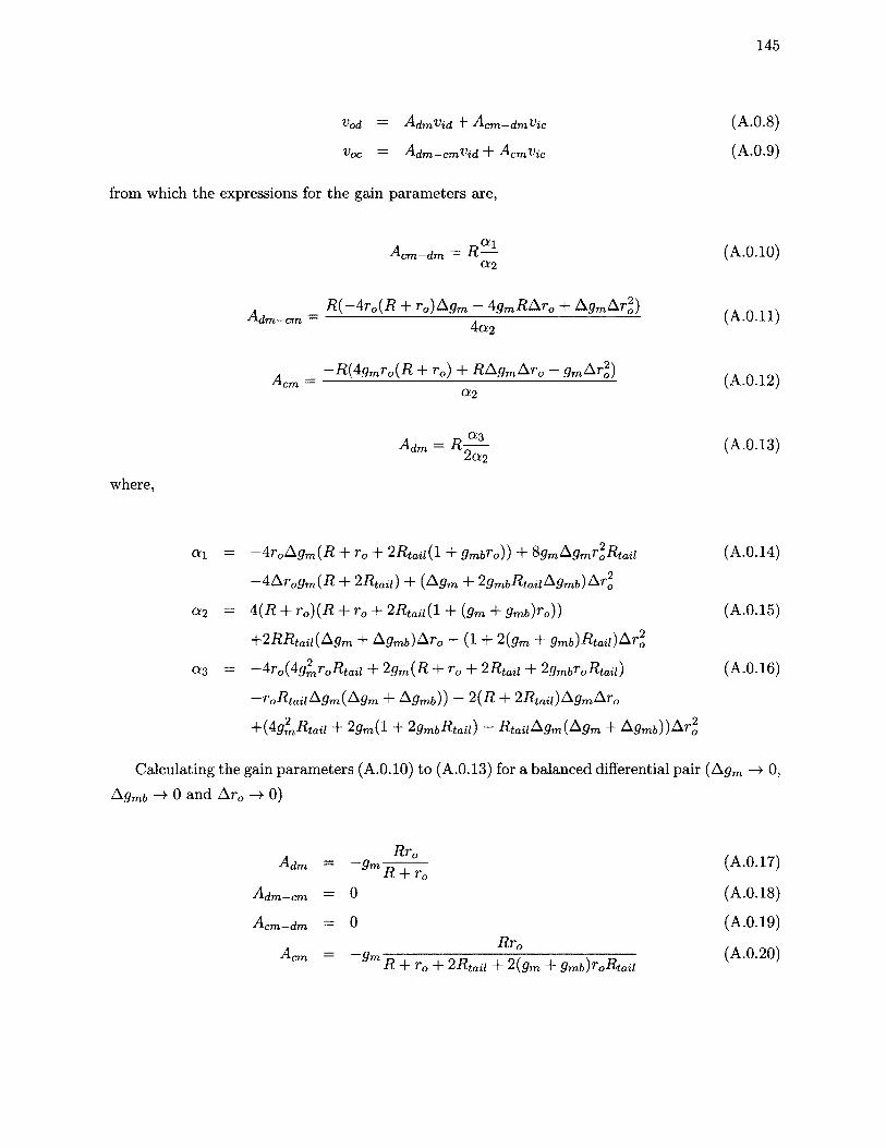
145
Vod — AdmVid "I" -^cm—dm^tc (A.0.8)
Voc = A d m —cmVid + A cm Vic (A.0.9)
from which the expressions for the gain parameters are,
C t iA c m —d m — R (A.0.10)
C t 2
_ R {-A r0{R + r0)Agm - AgmR A r0 + AgmA r 20)A d m —c m — A (A.U.llj
4 a 2
A = -R (A gmr0(R + rQ) + R A g mA r 0 - gmA r 20) QCm C t 2
A dm = R ~ (A.0.13)2Ct2
where,
cti — Ar 0A gm{R + rQ + 2Rtau{\ 4~ g-mbfo)) 4- &9 mAgmr0Rtan (A.0.14)
4A r0gm(i? 4- 2Rtaii) 4“ {Agm 4- 2grnf>RtanAgrni})Ar0
ct2 = 4(i? + r 0)( i? 4 -r0 4 -2i?tai;( l 4 - (ffm 4-gm6)r0)) (A.0.15)
+2RRtati(Agrn + Agmf )Ar0 (1 4“ 2(gm 4~ gmb)RtaU)ArG
ct3 = Ar 0(Agmr 0Rtau 4- 2gm(R 4- r c 4- 2Rtan 4- 2gmbr0Rtaii) (A.0.16)
r'oRtaii Agm (Agin + Agmb)) 2(7? + 2R.ian) AgniAr 0
A (A g m R ta ii 4- 2<?m(l 4~ 2 g m \jR taii} ~ R - ta i lA g m {A g m 4~ A<7mf,))Ar0
Calculating the gain parameters (A.0.10) to (A.0.13) for a balanced differential pair (Agm —> 0,
Agmb ~t 0 and A r0 -> 0)
RrA d m = (A.0.17)R + r0
A d m - c m = 0 (A.0.18)
Acm-dm = 0 (A.0.19)R ,v
A-cm — — <7m p , _i_ O Z? T~o7 T \ p (A .0.20)R To 2Rfail 2 (<7m +
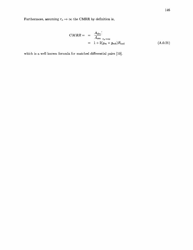
146
Furthermore, assuming r G —> oo the CMRR by definition is,
C M R R = = Adncm r 0—Hx>
1 + 2 ( g 771 4" 9 m b )R ta il
which is a well known formula for matched differential pairs [10].
(A.0.21)

Appendix B
PC B CAD
147
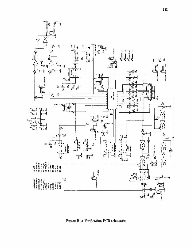
148
'10 Q nio QHI«r4 H te-^< i a <x z a
-U«r*§
a <§ s I- s ar 2t sr
i S ? ? ? 5 5 5i <4 r*> <-> ‘-1 UJ
Figure B .l: Verification PCB schematic

149
Figure B.2: Verification PCB layout, top later.
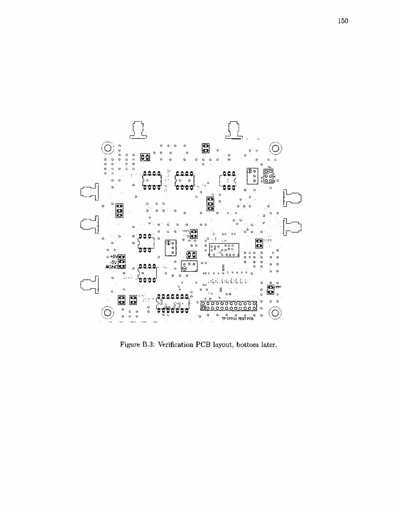
o o o o o o o
o o
o o
Lr o 1
0 ovx.
□ Jo0 z 0 00 00
00
0
0 0
o
o
o + 5V-5 V
AGNC
oOO
o
o
(Dooo
i VA|Ojolol
° o o o o o o o 000 '> 0 o 0 0
b p o o co0 0 0 0 o
0 0 0 0 0 00 0 0
o o00 0 O G 0 0 0 0 c
o o o o
0 0 0 0 0 0 0 0 0 0 0 0 o l o 0 0 0 0 0 0 0 0 0 0
TF CFP24 TEST PCB
o o jo'jcgro
(5)
Figure B.3: Verification PCB layout, bottom later.

Bibliography
[1] F . R a a b , “A v e rag e e ffic iency o f c lass-g p o w er a m p lif ie rs ,” C onsum er Electronics, IE E E Transactions on, vol. C E -3 2 , p p . 145 -1 5 0 , m a y 1986.
[2] T . K o b a y ash i, K . N o g a m i, T . S h iro to r i, a n d Y . F u jim o to , “A c u rre n t-c o n tro l le d la tc h se n se am p lif ie r a n d a s ta t ic p o w e r-sa v in g in p u t b u ffer fo r low -pow er a r c h i te c tu re ,” Solid-S tate Circuits, IE E E Journal of, vol. 28, p p . 523 -5 2 7 , a p r 1993.
[3] G . M o o re , “C ra m m in g m o re c o m p o n e n ts o n to in te g ra te d c irc u its ,” Electronics M agazine, vol. 38 , A p r 1965.
[4] “In te rn a tio n a l te c h n o lo g y ro a d n m a p fo r s e m ic o n d u c to rs ,” IT R S 2011 E d itio n .
[5] W . S an se n , “A n a lo g d e s ig n c h a llen g es in n a n o m e te r C M O S tec h n o lo g ie s ,” in Proc. IE E E A sian Solid-S tate Circuits Conference, p p . 5 -9 , N ov. 2007.
[6] T . M o u to n a n d B . P u tz e y s , “D ig ita l c o n tro l o f a P W M sw itc h in g a m p lif ie r w ith g lo b a l feed b a ck ,” in Audio Engineering Society Conference: 37th In ternational Conference: Class D A udio Am plification, p p . 108—117, 8 2009.
[7] T . F o rz ley a n d R . M a so n , “A low p o w er C la ss D a u d io a m p lif ie r sy s te m w ith d isc re te t im e lo o p f i lte r c o m p e n sa t io n ,” in C ircuits and S ystem s and TAISA Conference, 2009. N E W C A S-T A ISA ’09. Jo in t IE E E N orth-E ast Workshop on, p p . 1 -4 , J u n e 2009.
[8] P . N uzzo , C . N a n i, C . A rm ie n to , A . S a n g io v an n i-V in ce n te lli, J . C ra n in c k x , a n d G . V an d e r P la s , “A 6 -B it 5 0 -M S /s T h re s h o ld C o n fig u rin g S A R A D C in 9 0 -n m D ig ita l C M O S ,” Circuits and System s I: Regular Papers, IEEE Transactions on, vo l. 59, ja n . 2012.
[9] T . F o rz ley a n d R . M aso n , “A sc a la b le c lass d a u d io a m p lif ie r fo r low p o w er a p p lic a tio n s ,” in A udio Engineering Society Conference: 37th In ternational Conference: Class D A udio Am plification, p p . 1 1 -2 0 , 8 2009.
[10] P . R . G ra y a n d R . G . M ey er, A nalysis and Design of Analog Integrated Circuits, pp . 2 1 5 -2 3 8 . J o h n W ile y a n d Sons, fo u r th e d ., 2001.
[11] F . R u m sey , “C la ss d p o w er a m p lif ic a tio n ,” J. Audio Eng. Soc, vol. 57, no . 12, p p . 1 0 8 7 -1 0 9 3 , 2009.
[12] N . J a y a n t, J . J o h n s to n , a n d R . S a fran e k , “S ig n a l c o m p re ss io n b a se d on m o d e ls o f h u m a n p e rc e p tio n ,” P roceedings of the IEEE, vol. 81, p p . 1385 -1 4 2 2 , o c t 1993.
[13] K . N ie lsen , “A re v ie w a n d c o m p a riso n o f p u lse w id th m o d u la t io n (p w m ) m e th o d s fo r a n a lo g a n d d ig ita l in p u t sw itc h in g p o w er a m p lif ie rs ,” in Proc. 102nd A E S C onvention, p re p r in t 4446 , M a rch 1997.
[14] B .-H . G w ee, J . C h a n g , a n d V . A d r ia n , “A m ic ro p o w e r lo w -d is to r tio n d ig ita l C la ss-D am p lif ie r b a se d on a lg o rith m ic p u ls e w id th m o d u la to r ,” IEEE Trans, on C ircuits and System s, vol. 52, p p . 2 0 0 7 -2 0 2 1 , O c t. 2005.
[15] C . P a sc u a l et a i , “H ig h -fid e lity P W M in v e r te r for d ig ita l a u d io a m p lif ic a tio n : s p e c tra l a n a ly s is , re a l t im e D S P im p le m e n ta t io n a n d r e s u l ts ,” IE E E Trans. P ow er Electron., vol. 18, p p . 4 7 3 -4 8 5 , J a n . 2003.
[16] M . Jo h a n se n a n d K . N ie lsen , “A rev iew a n d c o m p a riso n o f d ig ita l P W M m e th o d s fo r d ig ita l p u lse m o d u la t io n am p lif ie r (P M A ) sy s te m s ,” in Proc. 107th A E S C onvention, p r e p r in t 5039, S e p t. 1999.
[17] R . S. S .R . N o rsw o rth y a n d G . T em es, D elta-Sigm a D ata C onverters, Theory, Design and Sim ulation. P is c a t- aw ay, N J : IE E E P re s s , 1997.
[18] T . S a m p ei, S. O h a sh i, Y . O h ta , a n d S. In o u e , “H ig h e s t e ffic iency a n d s u p e r q u a li ty a u d io am p lif ie r u s in g m os p o w er fe ts in c lass g o p e r a t io n ,” Consum er Electronics, IE E E Transactions on, vol. C E -2 4 , p p . 300 -3 0 7 , aug . 1978.
151
152
[19] N . A . Sokol a n d A . D . Sokol, “C la s s -E A n ew c la ss o f h ig h -effic ien cy tu n e d sin g led e n d e d sw itc h in g p o w er am p lif ie rs ,” IEEE J. Solid S ta te Circuits, vol. S C -1 0 , p p . 1 6 8 -1 7 6 , J u n e 1975.
[20] M . A . F . C h r is te n s e n , T . F re d e rik se n a n d K . N ie lsen , “P ra c tic a l im p le m e n ta t io n a n d e r ro r a n a ly s is o f P S C P W M b a se d sw itc h in g a u d io a m p lif ie rs ,” in Proc. 101th A E S Convention, p re p r in t 5040 , S e p t. 1999.
[21] M . A lb u le t , R F P ow er A m plifiers, p p . 2 -4 . A t la n ta , G A : N o b le P u b lish in g , f irs t e d ., 2001.
[22] C . P l e t t a n d J . R o g e rs , R adio Frequency Integrated C ircuit Design, p p . 2 8 6 -3 2 1 . N o rw o o d , M A : A rte c h H o u a se , f irs t e d ., 2003.
[23] K . N e ilsen , Audio pow er am plifier techniques w ith energy efficient pow er conversion. P h D th e s is , T ec h n ic a l U n iv e rs ity o f D e n m a rk , 1998.
[24] D . Z w illin g er, C R C Standard M athem atical Tables and Formula. C h a p m a n a n d H a ll, 3 1 st e d ., 2002.
[25] K . N ie lsen , “L in e a r ity a n d effic iency p e rfo rm a n c e o f sw itc h in g a u d io p o w e r am p lif ie r o u tp u t s ta g e s -a fu n d a m e n ta l a n a ly s is ,” in A udio Engineering Society Convention 105, 9 1998.
[26] I. M osely , P . M ello r, a n d C . B in g h a m , “E ffec t o f d e a d t im e o n h a rm o n ic d is to r tio n in c la ss -d a u d io p o w er a m p lif ie rs ,” Electronics Letters, vol. 35, p p . 950 -9 5 2 , ju n 1999.
[27] F . K o eslag , H . d u T . M o u to n , H . B eu k es , a n d P. M id y a , “A d e ta i le d a n a ly s is o f th e effec t o f d e a d t im e on h a rm o n ic d is to r tio n in a c la ss D a u d io a m p lif ie r ,” in Proc. IE E E A F R IC O N , pp . 1 -7 , S e p t. 2007.
[28] R . C . D o rf, M odem Control System s. R e a d in g , M A : A d d iso n -W esley , 1989.
[29] G . F . F ra n k lin a n d J . D . P o w ell, D igita l Control o f D ynam ic System s. M en lo P a rk ,C A : A d d iso n -W esley , t h i r d e d ., 1998.
[30] S. C . C r ip p s , R F P ow er A m plifiers fo r W ireless Com m incations. N o rw o o d , M A : A rte c h H o u se , f irs t e d ., 1999.
[31] M . B e rk h o u t a n d L. D o o p e r , “C la ss -d a u d io a m p lif ie rs in m o b ile a p p lic a t io n s ,” Circuits and S ystem s I: Regular Papers, IE E E Transactions on, vol. 57, p p . 992 -1 0 0 2 , m a y 2010.
[32] M . B e rk h o u t, L. B reem s, a n d E . v a n T u ijl, “A u d io a t low a n d h ig h p o w e r,” in Solid-S tate C ircuits Conference, 2008. E SSC IR C 2008. 34th European, p p . 40 -4 9 , s e p t. 2008.
[33] M . A . E . N . K . C h r is te n s e n , F ra n k S.; F re d e rik sen ; T h o m a s M .; A n d e rse n , “P ra c tic a l im p le m e n ta t io n a n d e r ro r a n a ly s is o f p scp w m b a se d sw itc h in g a u d io p o w er a m p lif ie rs ,” in A udio Engineering Society Convention 107, 9 1999.
[34] V . T o u si, F . S a h a n d i, M . A ta ro d i, a n d M . S h o ja e i, “A 3.3 v /1 w c la s s d a u d io p ow er a m p lif ie r w ith 103 d b d r a n d 90% efficiency,” in M icroelectronics, 2002. M IEL 2002. 23rd In ternational Conference on, vol. 2 , p p . 581 -5 8 4 , 2002.
[35] D . C a r ta s e g n a , P . M a lco v a ti, L. C re sp i, K . L ee, L. M u ru k u t la , a n d A . B a sc h iro tto , “A n a u d io 9 1 -d b th d th i rd -o rd e r fu lly -d iffe re n tia l c la ss -d a m p lif ie r ,” in E SSC IR C (E SSC IR C ), 2011 Proceedings of the, p p . 91 -9 4 , s e p t. 2011.
[36] J . J e o n g , H . S eong , J . Y i, a n d G . C h o , “A c la ss d sw itc h in g p o w er am p lif ie r w ith h ig h effic iency a n d w id e b a n d w id th b y d u a l fe ed b a ck lo o p s ,” in C onsum er Electronics, 1995., Proceedings of In ternational Conference on, p p . 428 -4 2 9 , 7-9 1995.
[37] A . O liv a , S. A n g , a n d T . Vo, “A m u lti- lo o p v o lta g e fe ed b a ck filte rle ss c la ss -d sw itc h in g a u d io a m p lif ie r u s in g u n ip o la r p u ls e -w id th -m o d u la t io n ,” C onsum er Electronics, IEEE Transactions on, vol. 50, p p . 312 - 319 , feb 2004.
[38] J . C h a n g , B . H . G w ee, Y . S . L o n , a n d M . T . T a n , “A novel lo w -p o w er low -v o ltag e c la ss d a m p lif ie r w ith fe ed b a ck fo r im p ro v in g th d , p o w e r effic iency a n d g a in lin e a rity ,” in C ircuits and System s, 2001. IS C A S 2001. The 2001 IEEE In ternational Sym posium on, vol. 1, p p . 635 -6 3 8 vol. 1, m ay 2001.
[39] M . R o ja s -G o n z a le z a n d E . S an ch ez -S in en c io , “L o w -p o w er h igh -effic iency class d a u d io p o w er a m p lif ie rs ,” Solid-S tate Circuits, IE E E Journal of, vol. 44, p p . 3272 -3 2 8 4 , dec. 2009.
[40] P . A n d re a n i, K . C h a o , M . P a te , a n d L. R isb o , “D is to r t io n a n d e r ro r re d u c tio n in a c la ss -d p o w e r s ta g e u s in g fe ed b a ck ,” in Audio Engineering Society Conference: 21th In ternational Conference: E fficient A udio P ow er Amplification, 9 2005.

153
[41] S. M . M u n k a n d K . S. A n d e rse n , “S ta te o f th e a r t d ig ita l p u lse m o d u la te d a m p lif ie r sy s te m ,” in Audio Engineering Society Conference: 23rd In ternational Conference: Signal Processing in A udio Recording and Reproduction , 5 2003.
[42] Y . F u jim o to , P. R e , a n d M . M iy a m o to , “A d e lta -s ig m a m o d u la to r fo r a 1 -b it d ig i ta l sw itc h in g a m p lif ie r ,” Solid-S tate Circuits, IEEE Journal of, vol. 40, p p . 1865 - 1871, s e p t. 2005.
[43] E . G a a la a s , B . L iu , N . N ish im u ra , R . A d a m s, a n d K . S w e e tla n d , “I n te g ra te d s te re o d e lta -s ig m a c la ss d am p lif ie r ,” Solid-State Circuits, IEEE Journal of, vol. 40, p p . 2388 - 2397, dec. 2005.
[44] Y . C h o i, W . T ak , Y . Y oon , J . R o h , S. K w o n , a n d J . K o h , “A 0 .018% t h d + n , 8 8 -d b p s r r p w m c la ss -d am p lif ie r fo r d ire c t b a t t e ry h o o k u p ,” Solid-State Circuits, IE E E Journal of, vol. 47, p p . 454 -4 6 3 , feb . 2012.
[45] J . T o rres , A . C o lli-M en ch i, M . R o ja s -G o n z a ? an d le z , a n d E . S a? a n d n c h e z S in en cio , “A 470 u w c lo ck -free c u rre n t-c o n tro lle d c la ss d a m p lif ie r w ith 0 .02% t h d + n a n d 8 2 d b p s r r ,” in ESSCIRC , 2010 Proceedings of the, p p . 326 -3 2 9 , se p t. 2010.
[46] J . V a ro n a , A . H a m o u i, a n d K . M a r t in , “A lo w -v o ltag e fu lly -m o n o lith ic d e lta -s ig m a b a se d c la ss -d a u d io a m p lifier,” in Solid-State C ircuits Conference, 2003. E SSC IR C ’03. Proceedings o f the 29th European, p p . 545 -5 4 8 , s e p t. 2003.
[47] V . A n tu n e s , V . P ire s , a n d J . S ilva, “D ig ita l m u ltile v e l a u d io p o w e r a m p lif ie r w ith a m a s h s ig m a -d e lta m o d u la to r to re d u c e h a rm o n ic d is to r t io n ,” in Industrial Electronics, 2005. ISIE 2005. Proceedings o f the IEEE In ternational Sym posium on, vol. 2, pp . 525 - 528, ju n e 2005.
[48] C . N e esg aa rd , R . A n tley , T . E fla n d , C . K a y a , K . M o ch izu k i, F . N y b o e , L. R isb o , D . S k e lto n , S. U n n ik ir is h n a n , a n d A . Z h ao , “C lass d d ig ita l p o w er a m p ( p u r e p a th d ig ita l) h ig h q m u s ica l c o n te n t ,” in P ow er Sem iconductor D evices and ICs, 200f . Proceedings. ISPSD ’Of ■ The 16th In ternational Sym posium on, p p . 97 - 100, m ay 2004.
[49] Y .-H . Lee, C .-K . Seok, B .-J . K im , S .-B . Y ou, W .-S . Y eum , H .-J . P a rk , Y .-H . J u n , B .-S . K o n g , a n d J .-W . K im , “A 1 .3-m w p e r-c h a n n e l 10 3 -d b s n r s te re o a u d io d a c w ith c la ss -d h e a d -p h o n e s a m p lif ie r in 6 5 n m c m o s ,” in VLSI Circuits, 2008 IE E E Sym posium on, p p . 176 -1 7 7 , ju n e 2008.
[50] M . W an g , X . J ia n g , J . S o n g , a n d T . B ro o k s , “A 120 d b d y n a m ic r a n g e 400 m w c la ss -d sp e a k e r d r iv e r w ith fo u r th -o rd e r p w m m o d u la to r ,” Solid-State Circuits, IEEE Journal of, vol. 45 , pp . 1427 -1 4 3 5 , au g . 2010.
[51] F . G u a n z iro li, R . B asso li, C . C r ip p a , D . D ev ecch i, a n d G . N ico llin i, “A lw 104 d b sn r filte r-le ss fu lly -d ig ita l o p e n -lo o p c la ss d a u d io a m p lif ie r w ith e m i r e d u c t io n ,” Solid-State Circuits, IEEE Journal of, vol. 47, p p . 686 -6 9 8 , m a rc h 2012.
[52] J .-M . L iu , S .-H . C h ie n , a n d T .-H . K u o , “A 100 w 5 .1 -c h a n n e l d ig ita l c la ss -d a u d io a m p lif ie r w ith s in g le -ch ip d e s ig n ,” Solid-State Circuits, IE E E Journal of, vol. 47, p p . 1344 -1 3 5 4 , ju n e 2012.
[53] K . P h ilip s , J . V . d e n H o m b e rg , a n d C . D ijk m a n s , “P o w erD A C : a s in g le -c h ip a u d io D A C w ith a 70% -efficient p o w er s ta g e in 0 .5 u m C M O S ,” in Proc. IE E E ISSC C , p p . 1 5 4 -1 5 5 , 1999.
[54] T . Id o , S. Ish izu k a , L. R isb o , F . A oyag i, a n d T . H a m a sa k i, “A d ig ita l in p u t c o n tro l le r fo r a u d io C lass-D a m p lif ie rs w ith 100W 0 .004% T H D + N a n d 113dB D R ,” in Proc. IEEE ISSC C , p p . 1366 -1 3 7 5 , feb. 2006.
[55] L . D o o p e r a n d M . B e rk h o u t, “A 3.4 w d ig ita l- in c la ss -d a u d io am p lif ie r in 0 .1 4 u m c m o s ,” Solid-S tate Circuits, IE E E Journal of, vol. 47, p p . 1524 -1 5 3 4 , ju ly 2012.
[56] P . M id y a , B . R o eck n e r, a n d A . B e rg s te d t , “D ig ita l c o rre c tio n o f P W M sw itc h in g a m p lif ie rs ,” IEEE P ow er Electronics Letters, vol. 2, p p . 6 8 -7 2 , J u n e 2004.
[57] S. R am asw am y , J . K r is h n a n , B . F o re jt, J . Jo y , M . B u rn s , a n d G . B u r ra , “A h ig h -p e rfo rm a n c e d ig ita l- in p u t c la ss -d am p lif ie r w ith d ire c t b a t t e r y c o n n e c tio n in a 9 0 n m d ig ita l cm o s p ro c e ss ,” in Solid-S tate Circuits Conference, 2008. ISSC C 2008. D igest o f Technical Papers. IEEE International, p p . 436 -6 2 5 , feb . 2008.
[58] P . D o n d o n a n d J . M ic o u le au , “A n o r ig in a l a p p ro a c h fo r th e d e s ig n o f a c la ss d p o w er sw itc h in g a m p lif ie r-an a u d io a p p lic a t io n ,” in Electronics, C ircuits and System s, 1999. Proceedings of IC E C S ’99. The 6th IEEE In ternational Conference on, vol. 1, pp . 161 -1 6 4 v o l . l , 1999.
[59] S. L o g an a n d M . H aw k sfo rd , “L in e a r iz a tio n o f c la ss d o u tp u t s ta g e s fo r h ig h -p e rfo rm a n c e a u d io p o w er a m p lifie rs ,” in Advanced A -D and D -A C onversion Techniques and their A pplications, 1994- Second In ternational Conference on, p p . 136 -1 4 1 , ju l 1994.

154
[60] “A D 7 7 6 0 d a t a sh e e t.”
[61] Z. L u k ic , H . W an g , a n d A . P ro d ic , “H ig h -freq u e n c y d ig ita l c o n tro lle r fo r D C -D C c o n v e r te rs b a se d o n m u lt i -b i t s ig m a -d e lta p u lse -w id th m o d u la t io n ,” in Proc. IE E E A PE C , p p . 35 -40, 2005.
[62] Y . M a ts u y a , K . U c h im u ra , I. A , a n d T . K a n e k i , “A 1 7 -b it o v e rsam p lin g D -to -A c o n v e rs io n te c h n o lo g y u s in g m u lt is ta g e n o ise sh a p in g ,” IEEE J. Solid S ta te Circuits, vol. 24, p p . 9 6 9 -9 7 5 , A u g . 1989.
[63] R . S c h re ie r a n d G . C . T em es, U nderstanding D elta Sigm a D ata C onverters, pp . 3 6 6 -3 7 2 . H o b o k en , N J : Jo h n W ile y a n d S o n s , 2005.
[64] I. F u jim o r i a n d T . S u g im o to , “A 1.5V 4 .1 m W d u a l-c h a n n e l a u d io d e lta -s ig m a D /A c o n v e r te r ,” IEEE J. Solid S ta te Circuits, vol. 33, p p . 186 3 -1 8 7 0 , D ec. 1998.
[65] L. C a rle y , “A n o ise -sh a p in g c o d e r to p o lo g y fo r 1 5 + b it c o n v e rte rs ,” Solid-S tate Circuits, IE E E Journal of, vol. 24, p p . 2 6 7 -2 7 3 , a p r 1989.
[66] A . S y ed , E . A h m e d , D . M ak sim o v ic , a n d E . A la rc o n , “D ig ita l p u lse w id th m o d u la to r a rc h i te c tu re s ,” in P ow er E lectronics Specialists Conference, 2004. P E S C 04■ 2004 IEEE 35th Annual, vol. 6, p p . 4689 - 4695 V ol.6, ju n e 2004.
[67] G . F . F ra n k lin a n d J . D . P ow ell, D igital Control o f D ynam ic System s. M en lo P a rk ,C A : A d d iso n -W esley , t h i r d e d ., 1998.
[68] A . P ro d ic , D . M ak sim o v ic , a n d R . E ric k so n , “D e sig n a n d im p le m e n ta t io n o f a d ig ita l p w m c o n tro lle r fo r a h ig h -f re q u e n c y sw itc h in g d c -d c p o w er c o n v e r te r ,” in Industrial Electronics Society, 2001. IE C O N ’01. The 27th A nnual Conference o f the IEEE, vol. 2 , p p . 893 -8 9 8 vo l.2, 2001.
[69] R . W . E ric k so n a n d D . M ak sim o v ic , Fundam entals o f P ow er Electronics. N ew Y o rk , N Y : S p rin g e r Sc ience, se c o n d e d ., 2001.
[70] R . W . E ric k so n a n d D . M ak sim o v ic , Fundam entals o f P ow er Electronics. N ew Y o rk , N Y : S p rin g e r Sc ience, se c o n d e d ., 2001.
[71] G . V il la r , E . A la rco n , J . M a d re n a s , F . G u in jo a n , a n d A . P o v ed a , “E n e rg y o p tim iz a tio n o f ta p e re d b u ffe rs for C M O S o n -c h ip sw itc h in g p o w er c o n v e r te rs ,” in Proc. IE E E ISCAS, p p . 4 4 5 3 -4 4 5 6 , M a y 2005.
[721 M . N em es , “D riv in g la rg e c a p a c ita n c e s in M O S L S I sy s te m s ,” Solid-S tate Circuits, IE E E Journal of, vol. SC - 19, p p . 1 5 9 -1 6 1 , F eb . 1984.
[73] R . V . d e P la ssc h e , CM OS Integrated A nalog-to-D igital and D igital-to-Analog C onverters, p p . 9 1 -9 2 . B o s to n , M A : K lu w e r A c ad e m ic , 2003.
[74] V . G ia n n in i , P . N uzzo , V . C h iro n i, A . B a s c h iro t to , G . V an d e r P la s , a n d J . C ra n in c k x , “A n 820 uw 9 b 4 0 m s /s n o is e - to le ra n t d y n a m ic -sa r a d c in 9 0 n m d ig i ta l c m o s ,” in Solid-State C ircuits Conference, 2008. ISS C C 2008. D igest o f Technical Papers. IEEE International, p p . 238 -6 1 0 , feb . 2008.
[75] J . C ra n in c k x a n d G . V an d e r P la s , “A 6 5 f j/c o n v e rs io n -s te p 0 - to -5 0 m s /s 0 -to -0 .7 m w 9 b c h a rg e -sh a r in g s a r a d c in 9 0 n m d ig ita l c m o s ,” in Solid-S tate C ircuits Conference, 2007. ISSC C 2007. D igest o f Technical Papers. IE E E International, p p . 246 -6 0 0 , feb . 2007.
[76] A . Im a n i a n d M . B a k h tia r , “A tw o -s ta g e p ip e lin e d p a ss iv e c h a rg e -sh a r in g S A R A D C ,” in C ircuits and System s, 2008. A P C C A S 2008. IEEE A sia Pacific Conference on, p p . 141 -1 4 4 , d ec . 2008.
[77] D . A . J o h n s a n d K . M a r tin , Analog Integrated C ircuit Design, p p . 2 0 0 -2 0 2 . J o h n W ile y a n d Sons, 1997.
[78] B . W ic h t , T . N irsch l, a n d D . S c h m itt-L a n d s ie d e l, “Y ie ld a n d sp eed o p tim iz a tio n o f a la tc h - ty p e v o lta g e sen se a m p lif ie r ,” Solid-S tate Circuits, IE E E Journal of, vol. 39, p p . 1148 - 1158, ju ly 2004.
[79] P . N u zzo , F . D e B e rn a rd in is , P . T e rre n i, a n d G . V an d e r P la s , “N oise a n a ly s is o f re g e n e ra t iv e c o m p a ra to rs fo r re c o n fig u ra b le a d c a rc h ite c tu re s ,” C ircuits and System s I: Regular Papers, IEEE Transactions on, vol. 55, p p . 1441 -1 4 5 4 , ju ly 2008.
[80] M .-J . L ee , W . D ally , a n d P . C h ia n g , “L o w -p o w er a rea -effic ien t h ig h -sp e ed i / o c irc u it te c h n iq u e s ,” Solid-S tate Circuits, IE E E Journal of, vol. 35, p p . 1 5 9 1 -1 5 9 9 , n o v 2000.
[81] G . V . d e r P la s , S. D e co u te re , a n d D . D o n n a y , “A 0 .1 6 p J /c o n v e rs io n -s te p 2 .5 m W 1 .2 5 G s /s 4 b A D C in 9 0 n m d ig ita l C M O S p ro c e ss ,” in Proc. IE E E ISSC C , p p . 2 3 1 0 -2 3 1 1 , Feb . 2006.

155
[82] P . N u zzo , G . V . d e r P la s , F . D e B e rn a rd in is , L. V . d e r P e r re a m d B . G y se lin ck x , a n d P. T e rre n i, “A 1 0 .6 m W /0 .8 p J p o w e r-sc a la b le l G S / s 4 b A D C in 0 .1 8 u m C M O S w ith 5 .8 g h z e rb w ,” in Proc. IEEE D esign A utom ation Conf., p p . 8 7 3 -8 7 8 , J u ly 2006.
[83] Y . T s iv id is a n d C . M c A n d re w , Operation and modeling o f the M O S transistor. N ew Y ork : O x fo rd U n iv e rs ity P re ss , th i r d e d ., 2011.
[84] T . C . C a ru so n e , D . A . J o h n s , a n d K . M a r t in , Analog Integrated C ircuit Design, p p . 3 8 4 -3 8 6 . J o h n W ile y a n d S o n s , seco n d e d ., 2012.
[85] I. O p ris , “N o ise e s t im a tio n in s t ro b e d c o m p a ra to r s ,” Electronics L etters, vol. 33, p p . 1273 -1 2 7 4 , ju l 1997.
[86] T . C . C a ru so n e , D . A . J o h n s , a n d K . M a r t in , Analog Integrated C ircuit D esign, p p . 4 1 3 -4 3 9 . J o h n W ile y a n d S o n s , seco n d e d ., 2012.
[87] A . B o n i, G . C h io rb o li, a n d C . M o ra n d i, “D y n a m ic c h a ra c te r is a t io n o f h ig h -sp e ed la tc h in g c o m p a ra to r s ,” Electronics Letters, vol. 36, p p . 402 -4 0 4 , m a r 2000.
[88] SSM 2517 D ata Sheet. A n a lo g D ev ices.
[89] M A X 9850 D ata Sheet. M a x im I n te g ra te d C irc u its .