analog output module user manual - rockwell...
TRANSCRIPT

����
�����
������ ������������
���� �� ������� ������ ��
�������������

Because of the variety of uses for the products described in thispublication, those responsible for the application and use of this controlequipment must satisfy themselves that all necessary steps have been takento assure that each application and use meets all performance and safetyrequirements, including any applicable laws, regulations, codesand standards.
The illustrations, charts, sample programs and layout examples shown inthis guide are intended solely for example. Since there are many variablesand requirements associated with any particular installation, Allen-Bradleydoes not assume responsibility or liability (to include intellectual propertyliability) for actual use based upon the examples shown in this publication.
Allen-Bradley publication SGI-1.1, “Safety Guidelines For TheApplication, Installation and Maintenance of Solid State Control”(available from your local Allen-Bradley office) describes some importantdifferences between solid-state equipment and electromechanical deviceswhich should be taken into consideration when applying products such asthose described in this publication.
Reproduction of the contents of this copyrighted publication, in whole orin part, without written permission of Allen-Bradley Company, Inc.is prohibited.
Throughout this manual we make notes to alert you to possible injury topeople or damage to equipment under specific circumstances.
ATTENTION: Identifies information about practices orcircumstances that can lead to personal injury or death, propertydamage or economic loss.
Attention helps you:
Identify a hazard. Avoid the hazard. Recognize the consequences.
Important: Identifies information that is especially important forsuccessful application and understanding of the product.
Important: We recommend you frequently backup your applicationprograms on appropriate storage medium to avoid possible data loss.
������� � �� �������

����� �� �����
���������� ��������� � �������� ���
����� �� �����
This release of the publication contains updated information from thelast release.
������ ������� ��
This publication covers the Series B version of the Analog Outputmodule.In addition, this version of the manual contains informationformally included in publication 1771-6.5.30–RN1, dated December1995.
A revised circuit board layout has the configuration jumpersrelocated from previous versions. Access holes are included in theside cover so that covers no longer have to be removed to adjust thejumpers or potentiometers.
The module also contains information on “Compliance to EuropeanUnion Directives.”
����� ����
To help you find new and updated information in this release of thepublication, we have included change bars as shown to the right ofthis paragraph.
������� � ������

SOC-2 Summary of Changes
���������� ��������� � �������� ���

�������
�3!*(" 2(-, ����7 ���� � �-4$+!$0 ����
�������
This manual shows you how to use the analog output module with anAllen-Bradley programmable controller. It describes methods forinstalling, programming, calibrating, and troubleshooting yourmodule.
To make efficient use of your module, you must be able to programand operate an Allen-Bradley programmable controller. Inparticular, you must be able to program block transfer instructions.
In this manual we assume that you know how to do this. If you donot, refer to the appropriate programming and operations manual forthe processor that you are using.
In this manual we refer to the:
• Analog Output Module (cat. no. 1771-OFE) as the “outputmodule”
• Programmable Controller as the “processor” or “controller.”
The manual is divided into seven chapters. The following chartshows each chapter with its corresponding title and a brief overviewof the topics covered in that chapter.
������ ����� ������ ������
��4$04($5 -% 2'$ �, *-& �32.32
�-#3*$
�$1"0(.2(-, -% 2'$ +-#3*$� (,"*3#(,& &$,$0 * ,#
' 0#5 0$ %$ 230$1� �-5 +-#3*$1 "-++3,(" 2$ 5(2'
.0-&0 ++ !*$ "-,20-**$01
�-#3*$ �,12 ** 2(-,�-5$0 0$/3(0$+$,21� )$6(,&� +-#3*$ *-" 2(-, ,# ' 0#7
5 0$ "-,%(&30 2(-,
�-#3*$ �-,%(&30 2(-,�-%25 0$ "-,%(&30 2(-,1� -32.32 0 ,&$ 1$*$"2(-,� # 2
%-0+ 2 ,# # 2 1" *(,&
� �-#3*$ �0-&0 ++(,&
�0(2(,& # 2 2- 2'$ +-#3*$� ,# -2'$0 .0-&0 ++(,&
"-,1(#$0 2(-,1 �#$% 3*2 !*-") *$,&2'� !*-") 20 ,1%$0
!-3,# 06 5-0#� ,# 5 2"'#-& 2(+$0�
� �-#3*$ �2 231 ,# �,.32 � 2 �$ #(,& # 2 %0-+ 2'$ +-#3*$
� *(!0 2(,& �-30 �32.32 �-#3*$ � *(!0 2(-, .0-"$#30$1
� �( &,-12("1 ,# �0-3!*$1'--2(,& �0-3!*$1'--2(,& �3(#$ %-0 .0-!*$+ #( &,-1(1
������ �������
�� �����
�������
���� ����������
PrefaceP–2
�0 (&!�/&+* � �3����� � �+1#) #- ����
�!!������# ��$��
� �,#!&$&!�/&+*.
� �(+!' �-�*.$#- 2&/% �&*&3���3� �*" ���3���� �-+!#..+-.
� ��/� �� (# �+-)�/.
You can install your output module in any system that usesAllen-Bradley programmable controllers that have block transfercapabilities and the 1771 I/O structure.
For more information on your programmable controllers, contactyour nearest Allen-Bradley office.
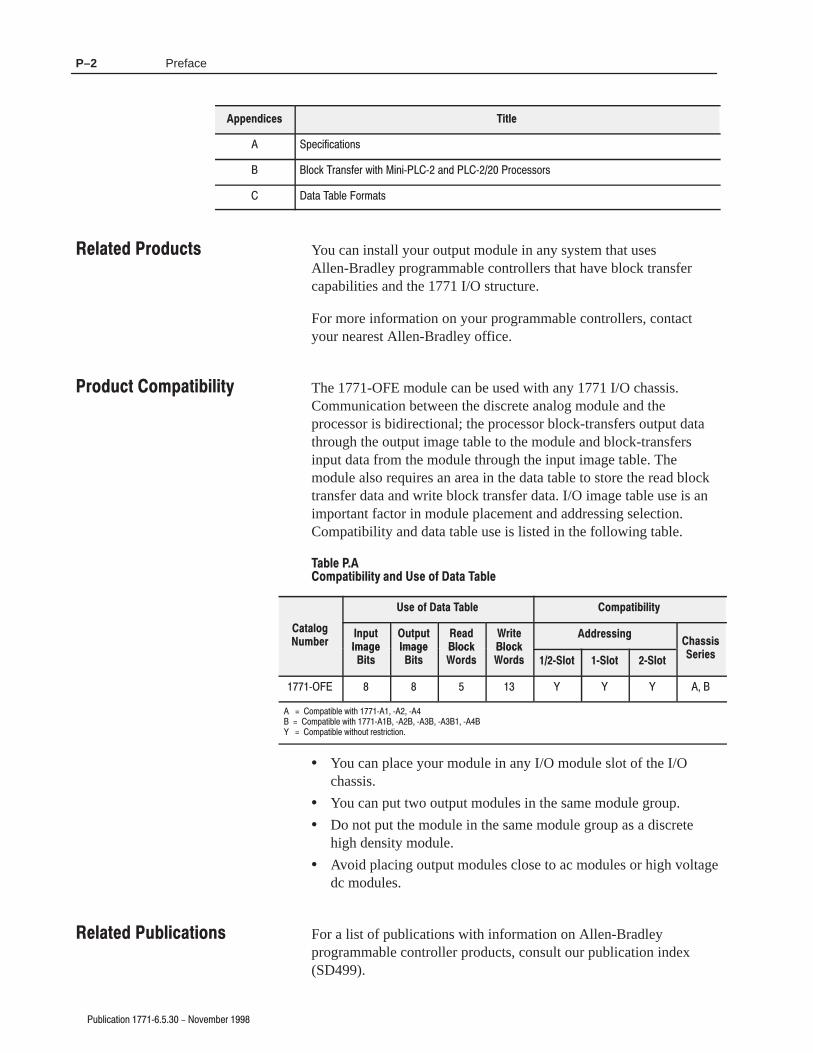
The 1771-OFE module can be used with any 1771 I/O chassis.Communication between the discrete analog module and theprocessor is bidirectional; the processor block-transfers output datathrough the output image table to the module and block-transfersinput data from the module through the input image table. Themodule also requires an area in the data table to store the read blocktransfer data and write block transfer data. I/O image table use is animportant factor in module placement and addressing selection.Compatibility and data table use is listed in the following table.
������ ��
� �!�$�����$& ��� �#� � �$� �����
�#� � �$� ����� � �!�$�����$&
��$�� �
�%���"�!%$
����
�%$!%$
����
����
�� ��
�"�$�
�� ��
���"�##������##�#
����
��$#
����
��$#
�� ��
� "�#
�� ��
� "�# ���'�� $ �'�� $ �'�� $��"��#
� �3��� � � � � � � � �� �
� � �+),�/& (# 2&/% � �3��� 3��� 3�
� � �+),�/& (# 2&/% � �3���� 3���� 3��� 3���� 3��
� � �+),�/& (# 2&/%+0/ -#./-&!/&+*�
• You can place your module in any I/O module slot of the I/Ochassis.
• You can put two output modules in the same module group.
• Do not put the module in the same module group as a discretehigh density module.
• Avoid placing output modules close to ac modules or high voltagedc modules.
For a list of publications with information on Allen-Bradleyprogrammable controller products, consult our publication index(SD499).
����$�� " �%�$#
" �%�$ � �!�$�����$&
����$�� %�����$� �#

�8&/-'%7-21 ����= ���� � �29)0&)5 ����
������ �
�,%37)5 �&.)'7-9)6 ���� � � � � � � � � � � � � � � � � � � � � � � � � � � � � � � � � � �
�2(8/) �)6'5-37-21 ���� � � � � � � � � � � � � � � � � � � � � � � � � � � � � � � � � � �
�2(8/) �)%785)6 ���� � � � � � � � � � � � � � � � � � � � � � � � � � � � � � � � � � �
�87387 �%1+)6 ��� � � � � � � � � � � � � � � � � � � � � � � � � � � � � � � � � � � �
�2: �1%/2+ �2(8/)6 �20081-'%7) :-7, �52+5%00%&/) �21752//)56 ��
�''85%'< ��� � � � � � � � � � � � � � � � � � � � � � � � � � � � � � � � � � � � � � � � � �
�,%37)5 800%5< ��� � � � � � � � � � � � � � � � � � � � � � � � � � � � � � � � � � � �
������ �
�,%37)5 �&.)'7-9)6 ��� � � � � � � � � � � � � � � � � � � � � � � � � � � � � � � � � � �
�203/-%1') 72
�8523)%1 !1-21 �-5)'7-9)6 ��� � � � � � � � � � � � � � � � � � � � � � � � � � �
��� �-5)'7-9) ��� � � � � � � � � � � � � � � � � � � � � � � � � � � � � � � � � � � � �
�2: "2/7%+) �-5)'7-9) ��� � � � � � � � � � � � � � � � � � � � � � � � � � � � � � � �
�)*25) $28 �167%// $285 �1%/2+ �2(8/) �� � � � � � � � � � � � � � � � � � � � �
�%/'8/%7-1+ �2:)5 �)48-5)0)176 �� � � � � � � � � � � � � � � � � � � � � � � � �
�)7)50-1) �2(8/) �2'%7-21 -1 7,) ��� �,%66-6 �� � � � � � � � � � � � � � � �
)77-1+ �2(8/) �21*-+85%7-21 �803)56 �� � � � � � � � � � � � � � � � � � � � �
�855)17 �87387 ")56-21 �� � � � � � � � � � � � � � � � � � � � � � � � � � � � � � �
"2/7%+) �87387 ")56-21 �� � � � � � � � � � � � � � � � � � � � � � � � � � � � � � �
�%67 7%7) �21*-+85%7-21 �803)56 �� � � � � � � � � � � � � � � � � � � � � � �
)77-1+ "2/7%+) �%1+) �21*-+85%7-21 �803)56 �����=���� 21/<� � �
�167%//-1+ 7,) �1%/2+ �2(8/) ��� � � � � � � � � � � � � � � � � � � � � � � � � � � � �
�211)'7-1+ #-5-1+ ���� � � � � � � � � � � � � � � � � � � � � � � � � � � � � � � � � � � �
�17)535)7-1+ 7,) �1(-'%725 �-+,76 ��� � � � � � � � � � � � � � � � � � � � � � � � � � �
�,%37)5 800%5< ��� � � � � � � � � � � � � � � � � � � � � � � � � � � � � � � � � � � �
������ �
�,%37)5 �&.)'7-9)6 ��� � � � � � � � � � � � � � � � � � � � � � � � � � � � � � � � � � �
�21*-+85-1+ $285 �2(8/) ��� � � � � � � � � � � � � � � � � � � � � � � � � � � � � � �
�21*-+85%7-21 #25( �� � � � � � � � � � � � � � � � � � � � � � � � � � � � � � � � � � �
�)*%8/7 �21*-+85%7-21 ��� � � � � � � � � � � � � � � � � � � � � � � � � � � � � � � � � �
�%7% �250%7 ��� � � � � � � � � � � � � � � � � � � � � � � � � � � � � � � � � � � � � � � �
'%/-1+ � � � � � � � � � � � � � � � � � � � � � � � � � � � � � � � � � � � � � � � � � � � � �
'%/-1+ "%/8) �2/%5-7< � � � � � � � � � � � � � � � � � � � � � � � � � � � � � � � � �
�%;-080 %1( �-1-080 '%/-1+ "%/8)6 � � � � � � � � � � � � � � � � � � � �
�52')(85) *25 �21*-+85-1+ $285 �2(8/) ��� � � � � � � � � � � � � � � � � � � � �
�,%37)5 800%5< ��� � � � � � � � � � � � � � � � � � � � � � � � � � � � � � � � � � � �
����� � �����
������� � ��� �����
����� ������
������ ����������
������ ��� ��������

Table of Contents��
�7$.+%#6+10 � �<����� � �18'/$'4 ����
������� �
�*#26'4 �$,'%6+8'5 ��� � � � � � � � � � � � � � � � � � � � � � � � � � � � � � � � � � �
�.1%- �4#05('4 9+6* 6*' �0#.1) �76276 �1&7.' ��� � � � � � � � � � � � � � � �
�.1%- �4#05('4 �41)4#//+0) �14/#65 ��� � � � � � � � � � � � � � � � � � � � � �
�.1%- �4#05('4 �41)4#//+0) < ���<� �#/+.; �41%'55145 �0.; ��� � � � �
�.1%- �4#05('4 �41)4#//+0) < ���< �#/+.; �41%'55145 �0.; ��� � � � �
�.1%- �4#05('4 �41)4#//+0) < ���<� �#/+.; �41%'55145 �0.; ��� � � � �
�6*'4 �41)4#//+0) �105+&'4#6+105 ���� � � � � � � � � � � � � � � � � � � � � � � �
�.1%- �'0)6* #0& �%#.+0) �105+&'4#6+105 ���� � � � � � � � � � � � � � � � �
�.1%- �4#05('4 �170 !14& < ���<� �#/+.; �41%'55145 �0.; ����
�1&7.' �2' �+/' ��� � � � � � � � � � � � � � � � � � � � � � � � � � � � � � � �
�;56'/ �:2#05+10 �'%1//'0+105 < ���<� �41%'55145 �0.; ��� � �
�*#26'4 �7//#4; ��� � � � � � � � � � � � � � � � � � � � � � � � � � � � � � � � � � � �
������� �
�*#26'4 �$,'%6+8'5 ���� � � � � � � � � � � � � � � � � � � � � � � � � � � � � � � � � � �
�'#&+0) �#6# (41/ 6*' �1&7.' ���� � � � � � � � � � � � � � � � � � � � � � � � � � �
�*#26'4 �7//#4; ���� � � � � � � � � � � � � � � � � � � � � � � � � � � � � � � � � � � �
������� �
�*#26'4 �$,'%6+8'5 ���� � � � � � � � � � � � � � � � � � � � � � � � � � � � � � � � � � �
�11.5 #0& �'56 �37+2/'06 ���� � � � � � � � � � � � � � � � � � � � � � � � � � � � � � �
�#.+$4#6+0) "174 �1&7.' ���� � � � � � � � � � � � � � � � � � � � � � � � � � � � � � � �
1.6#)' �76276 '45+10 �� �<����� ���� � � � � � � � � � � � � � � � � � � � � � �
�#.+$4#6+10 �41%'&74' ���� � � � � � � � � � � � � � � � � � � � � � � � � � � � � � �
�744'06 �76276 '45+10 �� �<����� ���� � � � � � � � � � � � � � � � � � � � � � �
�*#00'. �#.+$4#6+10 ���� � � � � � � � � � � � � � � � � � � � � � � � � � � � � � � � �
�744'06 �76276 '45+10
�� �<���� ���� � � � � � � � � � � � � � � � � � � � � � � � � � � � � � � � � � � � �
�*#00'. �#.+$4#6+10 ���� � � � � � � � � � � � � � � � � � � � � � � � � � � � � � � � �
�*#26'4 �7//#4; ����� � � � � � � � � � � � � � � � � � � � � � � � � � � � � � � � � � � �
������� �
�*#26'4 �$,'%6+8'5 ��� � � � � � � � � � � � � � � � � � � � � � � � � � � � � � � � � � �
�06'424'6+0) 6*' �0&+%#614 �+)*65 ��� � � � � � � � � � � � � � � � � � � � � � � � � � �
�'#& �.1%- �4#05('4 �6#675 !14&5 ��� � � � � � � � � � � � � � � � � � � � � � � �
�*#26'4 �7//#4; �� � � � � � � � � � � � � � � � � � � � � � � � � � � � � � � � � � � �
����� �����������
����� ������ ��� �����
����
����������� ���� �����
�����
����������� ���
��������������

Table of Contents ���
�2!*(" 1(-, ����6 ���� � �-3$+!$/ ����
�������! �
�.$"(%(" 1(-,0 ���� � � � � � � � � � � � � � � � � � � � � � � � � � � � � � � � � � � � � � �
�������! �
�2*1(.*$ ��� �,01/2"1(-,0 ���� � � � � � � � � � � � � � � � � � � � � � � � � � � � � � �
�2,& � ���� � � � � � � � � � � � � � � � � � � � � � � � � � � � � � � � � � � � � � � � � �
�2,&0 ,# ��� � � � � � � � � � � � � � � � � � � � � � � � � � � � � � � � � � � � �
�2,& �2++ /5 ��� � � � � � � � � � � � � � � � � � � � � � � � � � � � � � � � � � � �
�$11(,& 1'$ �*-") �$,&1' ��2*1(.*$ ��� �,01/2"1(-,0 �,*5� ��� � � � � � � �
�������! �
�6�(&(1 �(, /5 �-#$# �$"(+ * ����� ���� � � � � � � � � � � � � � � � � � � � � � �
�(&,$#6+ &,(12#$ �(, /5 ��� � � � � � � � � � � � � � � � � � � � � � � � � � � � � � �
�4-�0 �-+.*$+$,1 �(, /5 ��� � � � � � � � � � � � � � � � � � � � � � � � � � � � � �
�������������
����� �������� ���
����"��"� ��� ��"����
����������
���� ����� ������

Table of Contents��
���������� ��������� � �������� ���

������ �
�&�����%�! ��)����� � �!'����# ����
�������� �� �� � ��� ������������
Read this chapter to familiarize yourself with the analog outputmodule.
��� ���������� �� � ��
�!&% %�� �!�&�� � � � � � � � � � � � � � � � � � � � � � � � � � � � � � � � � ����
�!�&�� ���%&#�$ � � � � � � � � � � � � � � � � � � � � � � � � � � � � � � � � � ����
�&%"&% �� ��$ � � � � � � � � � � � � � � � � � � � � � � � � � � � � � � � � � � ����
�!( ��!� �!�&��$ �!��& ���%� (�%� �#!�#�������
�! %#!���#$ � � � � � � � � � � � � � � � � � � � � � � � � � � � � � � � � � � � � �
����
The Analog Output Module (cat. no. 1771-OFE) is an intelligentblock transfer module that converts binary or four-digit BCD values(supplied by your processor) to analog signals at its four moduleoutputs. The module accomplishes the data transfer with blocktransfer programming.
Block transfer write (BTW) programming moves up to 13 words ofdata from the processor to the module for digital to analog (D/A)conversion in one program scan. This information is converted toanalog signals and is sent to the appropriate output channels.
A block transfer read (BTR) moves five words of data from themodule to the processor data table, if desired, for diagnosticpurposes. The BTR is discussed in Chapter 7, “Diagnostics andTroubleshooting.”
The module has a scaling feature that converts data sent to themodule in engineering units to the proper analog signals.
You may connect up to four analog output devices--such as valvepositioners, motor speed controllers, signal converters orrecorders--to the analog output module’s four channels. All analogoutput device inputs should conform to the voltage or current ratingsof each module output channel.
�� ���� ���� �
�������
����� �� ����� ������
�����

����
�)�!���(�$# ����,����� � �$*�"��& ���
�� ��� ��������
In the programmable controller system, the analog output moduleprovides the following functions:
• four individually isolated differential outputs
• selectable scaling to engineering units
• selectable data format
• selectable voltage ranges (1771-OFE1 only)
• no external power required--power is drawn from the 1771 I/Ochassis backplane.
• requires only one I/O slot
����� �����
There are three versions of the analog output module:
������� ������ �� ��� ����� ����� ����
����,���� �$!(���
�,� ��
�,��� ��
���� ��
��!��(�� �+
�$#���)&�(�$#
)"%�&'
����,���� �)&&�#( ,��"� ���($&+ '�(
����,���� �)&&�#( �,�"� ���($&+ '�(
The voltage version (1771-OFE1) voltage output range is selectedwith configuration jumpers in the module:
Note: The 1771-OFE1 is shipped with the selection jumpers inthe +10V position.
The current output versions (1771-OFE2 and -OFE3) are factory set.

����
�(� ���'�#" ��*����� � �#)�!��% ����
The processor transfers data to the module (block transfer write) andfrom the module (block transfer read) using BTW and BTRinstructions in your ladder diagram program. These instructions letthe processor send output values to the module, establish themodule’s mode of operation (see illustration below) and receivestatus information from the module.
������������� ������� �������� ��� �����
+
–
2
13
�# �"� #� #('$(' ��)���&
���
�%#�%�!!�� �
�#"'%# �% "� #� �('$(' �#�( �
��'� �#� ��*���
���
���
4
5
1. The processor transfers your configuration and output data to themodule via a block transfer write instruction.
2. The module converts the data into proportional voltage or currentoutputs.
3. These module outputs drive external analog devices.
4. When instructed by your ladder program, the processor performsa read block transfer of output values and module status.
5. The processor and module determine that the transfer was madewithout error.
6. Your ladder program can use and/or move the data (if valid)before it is written over by the transfer of new data in asubsequent transfer.
The accuracy of your output module is described in Appendix A.
In this chapter you read about the functional aspects of the outputmodule and how the module communicates with the programmablecontroller.
��� ������ ������
����������� ����
�������� �� �����������
��������
������� �������

����
���������� ��������� � �������� ���

������ �
�2�)& �1&,+ ��6����� � �,3"*�"/ ����
�� �� ���������
In this chapter, you will read about:
��� ������ ���� �� ��� � ��
�,*-)&�+ " 1, �2/,-"�+ �+&,+ ��'" 1&3"0 � � � � � � � � � � � � � � ����
��) 2)�1" 1%" �,4"/ �".2&/"*"+10 � � � � � � � � � � � � � � � � � � � � ����
�"1 �,!2)" �,+#&$2/�1&,+ �2*-"/0 � � � � � � � � � � � � � � � � � � � � ����
�"5 1%" �� (-)�+" �,++" 1,/0 � � � � � � � � � � � � � � � � � � � � � � � ���
�+01�)) 1%" *,!2)" �+! �&")! �&/&+$ /* � � � � � � � � � � � � � � � � ����
�,++" 1 1%" �&/&+$ � � � � � � � � � � � � � � � � � � � � � � � � � � � � � � � �����
�/,2+! 1%" �%�00&0 �+! �,!2)" � � � � � � � � � � � � � � � � � � � � � � �����
Read this installation chapter completely before you install yourmodule. Double check all connections and option selections beforeyou begin programming your module.
!ATTENTION: To avoid injury to personnel anddamage to equipment, disconnect and lockout all acpower supplies before installing and wiring the outputmodule.
If this product has the CE mark, it is approved for installation withinthe European Union and EEA regions. It has been designed andtested to meet the following directives.
��� ���������
This product is tested to meet Council Directive 89/336/EECElectromagnetic Compatibility (EMC) and the following standards,in whole or in part, documented in a technical construction file:
• EN 50081-2EMC – Generic Emission Standard, Part 2 –Industrial Environment
• EN 50082-2EMC – Generic Immunity Standard, Part 2 –Industrial Environment
This product is intended for use in an industrial environment.
��� ���� �� ���������
This product is tested to meet Council Directive 73/23/EECLow Voltage, by applying the safety requirements of EN 61131–2Programmable Controllers, Part 2 – Equipment Requirements andTests.
�� � ��� �� ����
���� ���
������ ��� ��
������ � ���� ����������

����
�!����� ��� ��#����� � ��"����� ����
For specific information required by EN 61131-2, see the appropriatesections in this publication, as well as the following Allen-Bradleypublications:
• Industrial Automation Wiring and Grounding Guidelines ForNoise Immunity, publication 1770-4.1
• Guidelines for Handling Lithium Batteries, publication AG-5.4
• Automation Systems Catalog, publication B111
This equipment is classified as open equipment and must be mountedin an enclosure during operation to provide safety protection.
The analog output module receives its power through the 1771 I/Ochassis backplane from the chassis power supply. It does not requireany other external power supply. When planning your system, youmust consider the power usage of all modules in the I/O chassis toprevent overloading the I/O chassis backplane and/or power supply.Add this to the requirements of all other modules in the I/O chassis.
���� ������ ����� �����������
��#����� �� �� ��
��#�������� �� ��
��#���� ���� �� ��
!ATTENTION: Do not insert or remove modulesfrom the I/O chassis while system power is ON.Failure to observe this rule could result in damage tomodule circuitry.
������� �����
������������

����
���������� ��������� � �������� ���
You can place your module in any I/O module slot of the I/O chassiswith the following guidelines:
• Do not put the module in the same module group as a discretehigh-density module.
• Avoid placing output modules close to ac modules orhigh-voltage dc modules.
• Group output modules together within an I/O chassis wheneverpossible to minimize noise interference from other modules.
• You can put two output modules in the same module group.
The module configuration jumpers consist of:
• the last state configuration jumper (all versions)
• the voltage range configuration jumpers (1771-OFE1 only).
� ����� �� � �������
Current version modules (1771-OFE2 and -OFE3) have allconfiguration jumpers installed and require no additionalconfiguration. The configuration jumper for the Last State modeoutput level is in the default position (MID). See “Last StateConfiguration Jumpers” below.
������� �� � �������
If you are using the voltage output version, you need to set severalconfiguration jumpers on the module’s circuit board. You must setthese jumpers before you can proceed with configuring the module.When you set these jumpers, you configure each channel for one ofthe three voltage ranges listed above. The module is shipped withthe plugs in the +10V position.
��������� You do not have to remove the module cover to set theconfiguration jumpers
���� ����� ������ ������ �����
The LAST STATE configuration jumpers determine the value of allthe module’s outputs whenever communication between the moduleand the processor is lost. This condition occurs when a processor oradapter faults, or the processor is placed in the PROG or TESTmode, or if the remote I/O cable breaks.
��������� ��� ��
�������� �� ��� � �������
������� ��� ��
������ ������ �����
����
����������� ��"������ � �� ����� ���
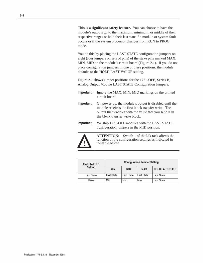
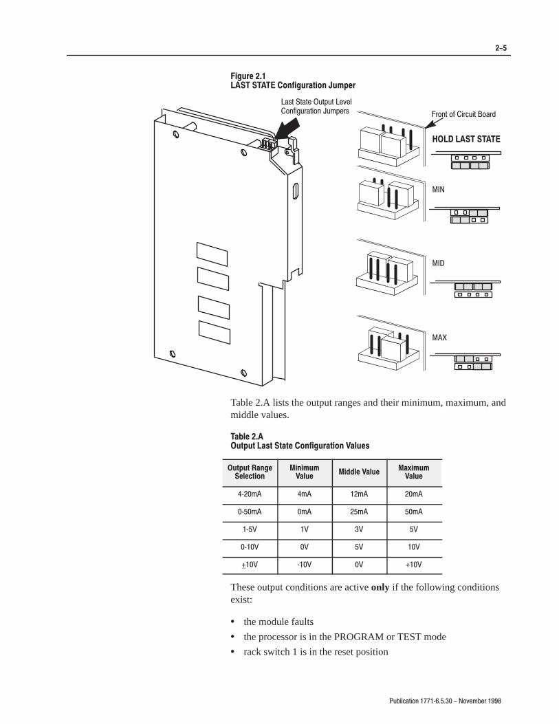
This is a significant safety feature. You can choose to have themodule’s outputs go to the maximum, minimum, or middle of theirrespective ranges or hold their last state if a module or system faultoccurs or if the system processor changes from RUN to PROGmode.
You do this by placing the LAST STATE configuration jumpers oneight (four jumpers on sets of pins) of the stake pins marked MAX,MIN, MID on the module’s circuit board (Figure 2.1). If you do notplace configuration jumpers in one of these positions, the moduledefaults to the HOLD LAST VALUE setting.
Figure 2.1 shows jumper positions for the 1771-OFE, Series B,Analog Output Module LAST STATE Configuration Jumpers.
��! "#��#� Ignore the MAX, MIN, MID markings on the printedcircuit board.
��! "#��#� On power-up, the module’s output is disabled until themodule receives the first block transfer write. Theoutput then enables with the value that you send it inthe block transfer write block.
��! "#��#� We ship 1771-OFE modules with the LAST STATEconfiguration jumpers in the MID position.
!ATTENTION: Switch 1 of the I/O rack affects thefunction of the configuration settings as indicated inthe table below.
���� �%�#�� �� ����$"�#� � $�!�" ��##���
��##������ �� ��� ��� ���� ����
���� ����� ���� ����� ���� ����� ���� ����� ���� �����
����� �� �� �! ���� �����
����
�.�&% �-%)( ����0����� � �)/"'�"+ ���
���%"�����
���� ���� � ����%"�$� � %�!�"
��,- �-�-" �.-*.- �"/"&
�)(#%$.+�-%)( �.'*"+,
���
���
���
�+)(- )# �%+ .%- �)�+!
��� ���� ����
Table 2.A lists the output ranges and their minimum, maximum, andmiddle values.
���������
�%$!%$ ��#$ �$�$� � ����%"�$� � ���%�#
�%$!%$ �����
�����$� �
�����%�
���%������� ���%�
��&��%�
���%�
0��'� '� ��'� ��'�
�0�'� �'� �'� �'�
�0� �� �� �
�0��� �� � ���
���� 0��� �� ����
These output conditions are active only if the following conditionsexist:
• the module faults
• the processor is in the PROGRAM or TEST mode
• rack switch 1 is in the reset position

����
�'�����&�"! ��*������ � �"(� ��$ ���
Rack switch 1 determines what output conditions occur during a rackfault.
���! �+ )�� �
� ))
%$� �*'�) %$ �*#&�' ��)) $�
��)) $���� ��� �� ���� ��� ����
��%& �&�&� ��%& �&�&� ��%& �&�&� ��%& �&�&� ��%& �&�&�
��%�& ��! ��� ��) ��%& �&�&�
To set the last state configuration jumpers, proceed as follows.
!ATTENTION: Do not insert modules into or removemodules from the I/O chassis while system power isON. Failure to observe this rule could result in damageto module circuitry and unexpected machine operation.
1. Locate the jumpers as shown in Figure 2.1.
2. Carefully pull up on the jumpers to remove from the pins.
3. Reposition as necessary to provide the value selected inTable 2.A.
��)) $� �%")��� ��$�� %$� �*'�) %$ �*#&�'( �����-� �� %$",�
If you ordered the voltage output version, you must set severalconfiguration jumpers located inside the module on the circuit board.To do this, follow these steps:
2. Locate the configuration jumpers and set them according to youroutput voltage requirements (Figure 2.3).
��%& �&�&� �'&#'& ��(��
"!���'$�&�"! �' #�$%
����%% �"��% �"$
"!���'$�&�"!
�' #�$%
5. Position the jumpers as indicated in Figure 2.3.

���
�4!+(" 3(.- ��8����� � �.5$,!$1 ���
���$!�����
�����$!�#��� �$� �! ����#���"
In
Out
�
�
�
�
�
�-
�-
�43
�43
�43
�43
����� ��
�43
�43
�-
�-
�43
�43
����
�43
�43
�43
�43
�-
�-
���
�
�
�-
�-
�43
�43
�43
�43
�43
�43
�-
�-
�43
�43
�43
�43
�43
�43
�-
�-
�-
�-
�43
�43
�43
�43
�43
�43
�-
�-
�43
�43
�43
�43
�43
�43
�-
�-
�-
�-
�43
�43
�43
�43
�43
�43
�-
�-
�43
�43
�43
�43
�43
�43
�-
�-
LAST STATE
�2(#$ 5($6
.% )4,/$1�
�.-%(&41 3(.-
�4,/$1
�." 3(.-
�$2(1$# �.+3 &$ � -&$ �43/43
�' --$+
��� �4,/$1
�
�
�
�
�
��� �4,/$1
�
�
�
�
�
��� �4,/$1
�
�
�
�
�
��� �4,/$1
!ATTENTION: Observe the followingprecautions when inserting orremoving keys:
• Insert or remove keys with yourfingers.
• Make sure the key placement iscorrect
Incorrect keying or the use of a tool canresult in damage to the backplaneconnector and possible system faults.
�+ "$ 3'$ *$7(-& ! -#2�
!$36$$- -# �
!$36$$- � -# ��
�.2(3(.- 3'$ *$7(-& ! -#2 (- 3'$ ! "*/+ -$ ".--$"3.12 3.
".11$2/.-# 3. 3'$ *$7 2+.32 .- 3'$ ,.#4+$�
�.4 " - "' -&$ 3'$ /.2(3(.- .% 3'$2$ ! -#2 (%
24!2$04$-3 2723$, #$2(&- -# 1$6(1(-& , *$2
(-2$13(.- .% #(%%$1$-3 37/$ .% ,.#4+$ -$"$22 17�
�//$1
�.--$"3.1
��� "' 22(2
��"#��� #�� ��%��� ����"

����
�0�(& �/&+* ��5�� ��� � �+1")�"- ���
!ATTENTION: Remove power from the 1771 I/Ochassis backplane and field wiring arm beforeremoving or installing an I/O module.
• Failure to remove power from the backplane orwiring arm could cause module damage, degradationof performance, or injury.
• Failure to remove power from the backplane couldcause injury or equipment damage due to possibleunexpected operation.
����
2&-&*$ �-)
�������
-")+1"
%+-&4+*/�( ��-
�//� % /%" 2&-&*$ �-) ���5��� /+ /%" %+-&4+*/�(
��- �/ /%" �+//+) +# /%" ��� %�..&.�
�%" 2&-&*$ �-) ,&1+/. 0,2�-! �*! +**" /. 2&/%
/%" )+!0(" .+ 3+0 �* &*./�(( +- -")+1" /%"
)+!0(" 2&/%+0/ !&. +**" /&*$ /%" 2&-".� ��5��
�
�2&*$ /%" %�..&. (+ '&*$ ��- !+2* &*/+ ,(� " /+ ." 0-"
/%" )+!0(".� ��'" .0-" /%" (+ '&*$ ,&*. "*$�$"�
��5��� 5��� 5���� 5���� 5��� ��� %�..&. ��5��� 5��� 5���� 5��� �"-&". � ��� %�..&.
(+ '&*$ /��
�-! $0&!".
)+!0("
)+!0("
����
�-! $0&!".
(+ '&*$ ��-(+ '&*$ ��- ,&*
�*�, /%" %�..&. (�/ % +1"-
/%" /+, +# /%" )+!0(" /+ ." 0-" &/�
�
������� �� ���� ��� �� ��
����� ���
���
�5",)#!4)/. ��:����� � �/6%-"%2 ���
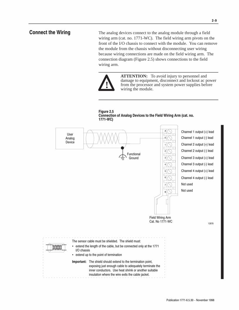
The analog devices connect to the analog module through a fieldwiring arm (cat. no. 1771-WC). The field wiring arm pivots on thefront of the I/O chassis to connect with the module. You can removethe module from the chassis without disconnecting user wiringbecause wiring connections are made on the field wiring arm. Theconnection diagram (Figure 2.5) shows connections to the fieldwiring arm.
!ATTENTION: To avoid injury to personnel anddamage to equipment, disconnect and lockout ac powerfrom the processor and system power supplies beforewiring the module.
���"������
�����!��� �� ������ ��#��� !� !�� ����� ������ ��� ���!� ���
��$� �
�
�
�
�
�
�
�
�(!..%, /54054 ��� ,%!$
�(!..%, /54054 �:� ,%!$
�(!..%, � /54054 ��� ,%!$
�(!..%, � /54054 �:� ,%!$
�(!..%, � /54054 ��� ,%!$
�(!..%, � /54054 �:� ,%!$
�(!..%, /54054 ��� ,%!$
�(!..%, /54054 �:� ,%!$
�/4 53%$
�/4 53%$
����
�)%,$ )2).' �2-
�!4� �/ ��: �
�(% 3%.3/2 #!",% -534 "% 3()%,$%$� �(% 3()%,$ -534�
• %84%.$ 4(% ,%.'4( /& 4(% #!",%� "54 "% #/..%#4%$ /.,9 !4 4(% ����� #(!33)3
• %84%.$ 50 4/ 4(% 0/).4 /& 4%2-).!4)/.
�����!��!� �(% 3()%,$ 3(/5,$ %84%.$ 4/ 4(% 4%2-).!4)/. 0/).4�
%80/3).' *534 %./5'( #!",% 4/ !$%15!4%,9 4%2-).!4% 4(%
)..%2 #/.$5#4/23� �3% (%!4 3(2).+ /2 !./4(%2 35)4!",%
).35,!4)/. 7(%2% 4(% 7)2% %8)43 4(% #!",% *!#+%4�
�3%2
�.!,/'
�%6)#%
�5.#4)/.!,
�2/5.$
�����! !�� ������
�����
�6#-*$"5*0/ ����; ���� � �07&.#&3 ����
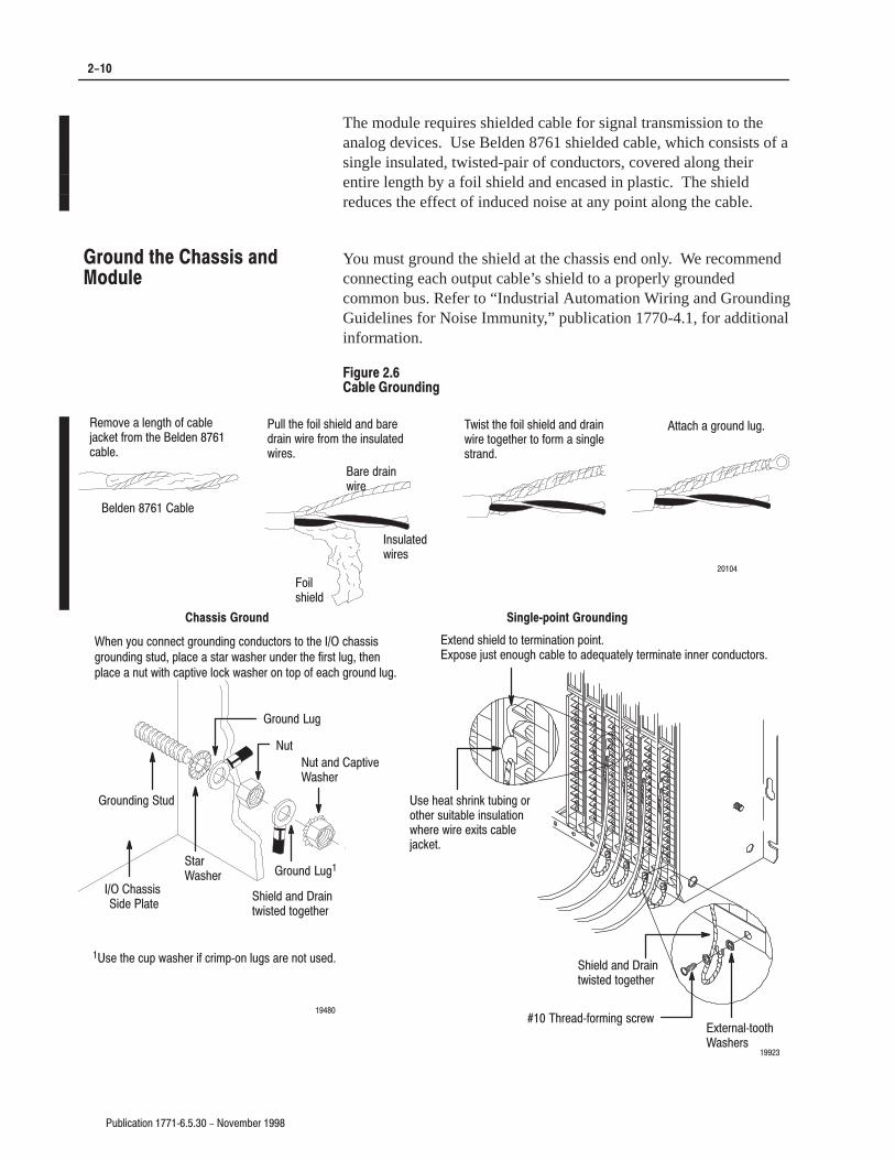
The module requires shielded cable for signal transmission to theanalog devices. Use Belden 8761 shielded cable, which consists of asingle insulated, twisted-pair of conductors, covered along theirentire length by a foil shield and encased in plastic. The shieldreduces the effect of induced noise at any point along the cable.
You must ground the shield at the chassis end only. We recommendconnecting each output cable’s shield to a properly groundedcommon bus. Refer to “Industrial Automation Wiring and GroundingGuidelines for Noise Immunity,” publication 1770-4.1, for additionalinformation.
���������
� ��� ��������
�&.07& " -&/(5) 0' $"#-&
+"$,&5 '30. 5)& �&-%&/ �� �
$"#-&�
�6-- 5)& '0*- 4)*&-% "/% #"3&
%3"*/ 8*3& '30. 5)& */46-"5&%
8*3&4�
�"3& %3"*/
8*3&
�/46-"5&%
8*3&4
�0*-
4)*&-%
�8*45 5)& '0*- 4)*&-% "/% %3"*/
8*3& 50(&5)&3 50 '03. " 4*/(-&
453"/%�
�55"$) " (306/% -6(�
����
�&-%&/ �� � �"#-&
�����
�306/%*/( �56%
� 4& 5)& $61 8"4)&3 *' $3*.1;0/ -6(4 "3& /05 64&%�
�� ���� �����
�306/% �6(
�306/% �6(��5"3
!"4)&3
��� �)"44*4
�*%& �-"5&
�65 "/% �"15*7&
!"4)&3
�95&3/"-;5005)
!"4)&34
��� �)3&"%;'03.*/( 4$3&8
���
�)*&-% "/% �3"*/
58*45&% 50(&5)&3
�)*&-% "/% �3"*/
58*45&% 50(&5)&3
������������ ��������
�95&/% 4)*&-% 50 5&3.*/"5*0/ 10*/5�
�9104& +645 &/06() $"#-& 50 "%&26"5&-: 5&3.*/"5& *//&3 $0/%6$5034�
4& )&"5 4)3*/, 56#*/( 03
05)&3 46*5"#-& */46-"5*0/
8)&3& 8*3& &9*54 $"#-&
+"$,&5�
�65
!)&/ :06 $0//&$5 (306/%*/( $0/%6$5034 50 5)& ��� $)"44*4
(306/%*/( 456%� 1-"$& " 45"3 8"4)&3 6/%&3 5)& '*345 -6(� 5)&/
1-"$& " /65 8*5) $"15*7& -0$, 8"4)&3 0/ 501 0' &"$) (306/% -6(�
����� ��� �� ���� ��
������

�����
�'�! ��& $# � �)����� � �$(�"��% ����
The front panel of the module contains a green RUN and a red FLT(fault) indicator. At power-up, the red FLT indicator lights andremains ON during an initial module self-check. If a fault is foundinitially or occurs later, the red FLT indicator stays lit. If a fault isnot found, the red indicator will turn off and the green RUNindicator will turn on and remain on.
Possible module fault causes and corrective actions are discussed inChapter 7, “Diagnostics and Troubleshooting.”
���������
�� ������� ���� ����
������
���
��� ����
���
���
� ��
In this chapter, you learned how to set the module configurationjumpers, connect the field wiring to the field wiring arm, and installyour module in the I/O chassis.
����������� ��� ���� ���
������
�� ���� ���� ��

�����
���������� ��������� � �������� ���

������ �
�*�#"��)"&% ����.����� � �&+�$��' ���
� ����� � �� ������� ����
In this chapter, you will read about:
�') "&�')%�+"'& '& ��� (� �
�&%�" *'"% �&*' �&�*#� � � � � � � � � � � � � � � � � � � � � � � � � � � � ����
�&%�" *'�)"&% �&'� � � � � � � � � � � � � � � � � � � � � � � � � � � � � � � � ����
����*#) �&%�" *'�)"&% � � � � � � � � � � � � � � � � � � � � � � � � � � � � � � ���
��)� �&'$�) � � � � � � � � � � � � � � � � � � � � � � � � � � � � � � � � � � � � ���
���#"% � � � � � � � � � � � � � � � � � � � � � � � � � � � � � � � � � � � � � � � � ����
�'&���*'� �&' �&%�" *'"% �&*' �&�*#� � � � � � � � � � � � � � � � � � ����
Because of the many analog devices available and the wide varietyof possible applications, you must configure the module to conformto the analog device and specific application that you have chosen.You do this with a block transfer write instruction (BTW). The writeblock can be up to 13 words long and contains output data andinformation on data format and scaling.
�')� �**" &%�&+ �') �$'�# �)�&*��) �)"+�
�')������ �"+ � �� �� �� �� �� � �� �� � � �� �� �� �� ��
�')����+�$ �"+ �� � � �� �� �� �� �� �� � � �� �� �� �� ��
� �!�%%�# � ��)� ��#*�
� �!�%%�# � ��)� ��#*�
� �!�%%�# � ��)� ��#*�
�!�%%�# ��)� ��#*�
��)� �&'$�) ��(�'+�� �"%"$*$���,"$*$ ���#"% ��#*� �&#�'")- ��)� �&#�'")-
� �!�%%�# � �"%"$*$ ���#"% ��#*�
� �!�%%�# � ��,"$*$ ���#"% ��#*�
�!�%%�# � �"%"$*$ ���#"% ��#*�
� �!�%%�# � ��,"$*$ ���#"% ��#*�
�� �!�%%�# � �"%"$*$ ���#"% ��#*�
�� �!�%%�# � ��,"$*$ ���#"% ��#*�
�� �!�%%�# �"%"$*$ ���#"% ��#*�
�� �!�%%�# ��,"$*$ ���#"% ��#*�
�%(')+�&+� A block transfer write length of 0 will result in a defaultlength of 13. A block transfer read length of 0 willresult in a default length of 5.
�!�+ �!"* �!�(+�)
�'&+�"&*
�'&�" ,)"& �',) �'�,$�

����
�(�! ��' $# � �,����� � �$)�"��% ����
Note: Programmable controllers that use 6200 softwareprogramming tools can take advantage of the IOCONFIG utility toconfigure this module. IOCONFIG uses menu-based screens forconfiguration without having to set individual bits in particularlocations. Refer to your 6200 software literature for details.
Programmable controllers that use process configuration andoperation software (cat. no. 6190-PCO) can take advantage of thosedevelopment and runtime tools used for the application ofprogrammable controllers in process control. The PCO worksheetsand the menu-driven configuration screens and faceplates let youconfigure, test/debug and operate the I/O module. Refer to your6190-PCO software literature for details.
The first four words in the BTW contain the actual data in binary orfour-digit BCD format, which is converted by the module intovoltage or current signals. When using the PLC-5, the 2’scomplement binary can be used provided the +10V range is not used.
�� ������� ���
����� ���������������
� ��,�� ���,� � ���##�! � ��'� ��!(�
� ��,�� ���,� � ���##�! � ��'� ��!(�
��,�� ���,� � ���##�! ��'� ��!(�
��,�� ���,� � ���##�! ��'� ��!(�
� �$#� �(%�' $# �$%� , %���% '$ � �(%���� ��!$*�
� ��,�� ���,� � ���##�! � � # "(" &��! #� )�!(�
��,�� ���,� � ���##�! � ��+ "(" &��! #� )�!(�
� ��,�� ���,� � ���##�! � � # "(" &��! #� )�!(�
� ��,�� ���,� � ���##�! � ��+ "(" &��! #� )�!(�
�� ��,�� ���,� � ���##�! � # "(" &��! #� )�!(�
�� ��,�� ���,� � ���##�! ��+ "(" &��! #� )�!(�
�� ��,�� ���,� � ���##�! � # "(" &��! #� )�!(�
� ��,�� ���,� � ���##�! ��+ "(" &��! #� )�!(�
Word 5 in the BTW is the module configuration word. Informationthat you enter in this word tells the module what data format toexpect and the polarity of the data and scaling values.
The remaining eight words (words 6 through 13) in the BTW arereserved for minimum and maximum scaling values. You enter thesevalues if you wish to scale a particular channel.

��
�.�&%��-%)( ����2 ���� � �)/!'�!+ ����
Word 5 of the block transfer write is the module configuration word(Figure 3.1). It contains information on:
• data polarity
• scaling polarity
• data format
� �*'����
�%$� �*'�) %$ �"%�! �'�$(��' �' )� �%'� �
�%'������ � ) �� �� � � �� �� �� �� �� � �� �� � � �� ��
�%'����)�" � ) �� � �� �� � � �� �� �� � �� �� � � �� ��
�)+ � � � � � � �
��-���)+'�-
�!,!+/!
�����%(�+1
�������
��0%'.'����&%(#���&.!��)&�+%-1
�����!#�-%/!
�����),%-%/!�%(%'.'����&%(#���&.!��)&�+%-1
�����!#�-%/!
�����),%-%/!
��-���%#(��)&�+%-1
�����!#�-%/!
�����),%-%/!
�����$�((!&��
����$�((!&�
����$�((!&�
�����$�((!&��
���
���"����
� )��%'� ��(�' &) %$( �%' �%$� �*'�) %$ �"%�! �'�$(��' �' )�
�%'� �
�%'���� #�" � )
���)�" � )���(�' &) %$
��2���-� *)&�+%-1 �%-,� �$!( ,!- ���� %( %��-! (!#�-%/! �-�� �$!( +!,!- ���� %( %��-!
*),%-%/! �-�� �%- �� �)++!,*)( , -) �$�((!& �� �%- �� -) �$�((!& � !-��
���$!( ,!- ���� %( %��-!, (!#�-%/! '%(%'.' ,��&%(# /�&.! ")+ �$�((!& �� �$!(
+!,!- ���� %( %��-!, *),%-%/! '%(%'.' ,��&%(# /�&.! ")+ �$�((!& ��
�
���$!( ,!- ���� %( %��-!, (!#�-%/! '�0%'.' ,��&%(# /�&.! ")+ �$�((!& �� �$!(
+!,!- ���� %( %��-!, *),%-%/! '�0%'.' ,��&%(# /�&.! ")+ �$�((!& ��
�
� �$!( ,!- ���� %( %��-!, (!#�-%/! '%(%'.' ,��&%(# /�&.! ")+ �$�((!& � �$!(
+!,!- ���� %( %��-!, *),%-%/! '%(%'.' ,��&%(# /�&.! ")+ �$�((!& �
���$!( ,!- ���� %( %��-!, (!#�-%/! '�0%'.' ,��&%(# /�&.! ")+ �$�((!& � �$!(
+!,!- ���� %( %��-!, *),%-%/! '�0%'.' ,��&%(# /�&.! ")+ �$�((!& �
�� �����$!( ,!- ���� %( %��-!, (!#�-%/! '%(%'.' ,��&%(# /�&.! ")+ �$�((!& � �$!(
+!,!- ���� %( %��-!, *),%-%/! '%(%'.' ,��&%(# /�&.! ")+ �$�((!& �
�%$� �*'�) %$ �%'�

����
�.�&%��-%)( ����2���� � �)/!'�!+ ����
��$�#�"%�! ������� �%
���%�� �%��!#�
� �����$!( ,!- ���� %( %��-!, (!#�-%/! '�0%'.' ,��&%(# /�&.! ")+ �$�((!& � �$!(
+!,!- ��� %( %��-!, *),%-%/! '�0%'.' ,��&%(# /�&.! ")+ �$�((!& �
� �����$!( ,!- ���� %( %��-!, (!#�-%/! '%(%'.' ,��&%(# /�&.! ")+ �$�((!& �� �$!(
+!,!- ��� %( %��-!, *),%-%/! '%(%'.' ,��&%(# /�&.! ")+ �$�((!& ��
�)+ �
�)(-%(.! �� �� ��$!( ,!- ���� %( %��-!, (!#�-%/! '�0%'.' ,��&%(# /�&.! ")+ �$�((!& �� �$!(
+!,!- ��� %( %��-!, *),%-%/! '�0%'.' ,��&%(# /�&.! ")+ �$�((!& ��
��2�� ���2��� �!,!+/!
�� �����$!( ,!- ���� -!&&, -$! ') .&! -) !0*!�- �%(�+1 �-�� �$!( +!,!- ��� ,%#(%"%!,
").+2 %#%- ��� �-��
At power-up, the module’s microprocessor assumes defaultconditions of:
• positive data words
• no scaling
• BCD data
The module’s microprocessor receives these values if you do notenter data into the configuration word:
The voltage or current value at one of the module’s outputs isdirectly proportional to the value specified in that channel’s dataword. The output scale is divided into 4095 parts, which means thatas the data word is incremented or decremented, the output signal isincremented or decremented 1/4095 of the full scale.
Table 3.B shows the incremented voltage or current assigned to eachbit for the four different output scales. For example, if the data wordfor Channel 1 contains the value 0000 0111 1111 1111 (2047decimal), the output for Channel 1 would be 2047/4095 orapproximately 1/2 of the full scale.
��������
�&%"&% �� ��$ � � ��$!�&%�!
�!�� �� �� �� � $����� �!�� �� �� �%&�� �&%"&% �� �� ∆ ���% !# ∆ ���%
� -) � /)&-, -) ��� � -) ��� ���� ���� '��%-
-) � /)&-, -) ��� -) ��� ���� ���� '��%-
2� -) �� /)&-, 2��� -) ���� 2� -) ���� ���� ���� '��%-
� -) � '� -) ��� � -) �� '� ���� � � '��%-
-) � '� -) ��� -) �� '� ���� ���� '��%-
����&�% �! ���&#�%�!
��%� !#��%

����
�0!('" /'+* ��3�� ��� � �+1$)!$- ���
Some examples of how to determine the value of the data wordneeded to produce the desired output voltage or current follow:
�0/,0/ � *&$ �3�)�
� / �+-) / ��� ��3��� �
�$.'-$# �0/,0/ �� )�
� ���'/ ������)���'/ �%-+) � !($�����
�$)$)!$-� �)� "+--$.,+*#. /+ ." ($ )'*')0)
��� )� 3 �)��
������)���'/
� �� �#$"') (� � ��� ��� ��� ���� �����
�� ��� �
You would enter 1410 (BCD) or 0001 0100 0001 0000 into the dataword in order to get an output of 9.5 mA.
�0/,0/ � *&$ �3��
� / �+-) / 3!'/ !'* -2 ��3����
�$.'-$# �0/,0/ ����
� ���'/ ���)���'/ �%-+) � !($�����
����
���)���'/
� ���� �#$"') (� � ���� � �� �� �!'* -2�
�� ��� �
You would enter 0000 1110 0110 1001 into the data word to get anoutput of 9.0V.
These values are loaded into the module’s memory, from theprocessor, with a block transfer write.
������� If you are using BCD data format, you must downloadvalues to the module in the BCD format and set thecorresponding data polarity bit (see Figure 3.1) if anegative output is desired.
������� If the binary data format is selected, data can bedownloaded in a binary or 2’s complement binary dataformat. If binary is used, the appropriate data polaritybit must be set to express a negative value. The 2’scomplement format expresses a negative value via thebit pattern.
If the processor input information governs the module’s outputs,remember that data written to the output module must fall withincertain limits. Both BCD and binary data must fall within the range+9999. You can use the negative ranges by setting the “negativedata” bits in word 5 of the BTW.

����
�)�"!��(!%$ ����-���� � �%*�#��& � �
Scaling is the conversion of unscaled data to engineering units--suchas gallons/minute, degrees centigrade, and pounds/square inch. Youcan use the scaling feature to send the data for each channel to themodule in an optional scaled value representing actual engineeringunits. This value is scaled by the module to a proportional binaryvalue before it is used by the corresponding channel. The resolutionof this data is one part in 4095.
The scaling feature is implemented by entering scaling values in thedata format selected in words 6 through 13 of the BTW.
���$"& ��$+� �'$�("*-
Bits 04 to 11 (04 to 13 octal) of the configuration word (word 5) inthe write block designate positive or negative scaling values(Figure 3.2). By setting the appropriate negative scaling bit in word5, you can scale negative data or enable a negative scaling value.The sign bits are ignored if a corresponding channel is not scaled.
�" +(�����
�'��*"'& '� ���$"& ��$+� �'$�("*- �"*) "& *!� �$'�# �(�&)��( �("*�
�'&�" +(�*"'&��'(�
�'(������ �"* � � �� �� �� �� �� � �� �� � � �� �� �� ��
�'(����*�$ �"* �� �� � � �� �� �� �� �� �� � � �� �� �� ��
�%&� � � � � � � � � � � � �
��(���%&#�(
��'�&*��
�����!$�&,
�������
��+!#)#����"!$����")���%"�&!(,
��������(!*�
�����%'!(!*��!$!#)#����"!$����")���%"�&!(,
��������(!*�
�����%'!(!*�
��(���!�$��%"�&!(,
��������(!*�
�����%'!(!*�
����� �$$�"��
����� �$$�"��
����� �$$�"��
����� �$$�"��
�����
��,"%+% �&� �"&"%+% ���$"& ��$+�)
Words 6-13 of the write block transfer contain maximum andminimum scaling values for each channel. Word 6 corresponds toChannel 1 scale minimum, word 7 to Channel 1 scale maximum,word 8 to Channel 2 scale minimum, and so on (Figure 3.3).
The maximum and minimum scaling values are the upper and lowerlimits for output data. The module’s microprocessor reads thesevalues and automatically scales output data from the write blocktransfer.
���$"&

����
�)�! ��( $# ����-����� � �$*�"��& ���
The largest value that you can enter for a maximum scaling value is9999. The smallest value you can enter for a minimum scaling valueis -9999 (the minus sign is implemented by setting the appropriatebit in the configuration word).
��������� The maximum scale value must be larger than theminimum scale value. If not, block transfers continuebut data is not acknowledged by the module’smicroprocessor. Outputs remain in their last statebefore the fault.
Even if you scale fewer than four channels, a full 13-word blocktransfer is performed.
When scaling, all scaling information must be entered into the datatable using the same format that the module sends to the data table.
� ��� �� �� ������ ��� ���� ��� ����� ������� !�� �� ���
��� �$&"�( ���
��' �$"%!�"�#(� #�&,
� �#�� ���# ()�� � #�&,� #�&,
��������� PLC-2 users should always use BCD format becausethe PLC-2 processor performs math functions usingBCD data. The PLC-3, PLC-5 and PLC-5/250 useinteger math, you should use 2”s complement binary forany data that will be used with math instructions(including PID and CAR routines). BCD format isusually reserved for display purposes only.
��� ������
������� �� ��"�� � ��� ����� � ������� ��� �� �� ��� ����� ����
���� �����������
� ���##�! � ��(� ��!)�
� ���##�! � ��(� ��!)�
� ���##�! � ��(� ��!)�
���##�! ��(� ��!)�
�$#� �)&�( $# �$&�
� ���##�! � � # ")" ���! #� ��!)�
� ���##�! � ��+ ")" ���! #� ��!)�
���##�! � � # ")" ���! #� ��!)�
� ���##�! � ��+ ")" ���! #� ��!)�
�� ���##�! � � # ")" ���! #� ��!)�
�� ���##�! � ��+ ")" ���! #� ��!)�
�� ���##�! � # ")" ���! #� ��!)�
�� ���##�! ��+ ")" ���! #� ��!)�

����
�-�$#��,#'& � �2����� � �'.�%��* ����
If you do not wish to scale a particular channel, set the scaling valuesas shown below.
�� "� � ����� ������ ��!�� �
������� ��� � ���
��� ����� �
������� ��� � ���
2��%�
�2�� ��� ����
�2���
��� ,' 2��� ��� 2����
� �"#+ �$+' *�)-#*�+ 1'- ,' +�, ,"� �((*'(*#�,� +#!& �#, #& ,"� �'& #!-*�,#'& /'*� '* ,"� %#&#%-%
+��$#&! .�$-��
For example, suppose you choose the 1 to 5 volt range and BCDdata format for your module. You have a thermocouple input thatreports a temperature between 100oC and 900oC back to yourprocessor. You would like this input temperature scale to correspondto an output meter scale.
You would enter the following minimum and maximum scalingvalues into Words 6 and 7 of the write block:
����� ����� ��� � ������ ��� � �� � ���������������
��� � ���
��,�*+��$� ���� ���'� ���� ���
��'� ��� � �
�0�%($��
�'*� � � ����
�'*� � ����
���'� ��� ���
�0�%($��
��,�*+��$� ��
��,�*+��$� ���
��'�
��'�
�����
����
����
���
��,�*+��$� �� ���'� ���� �
If the processor sends a data value to the module that corresponds to350oC, the value is scaled to the 100oC to 900oC range and thecorresponding output voltage for that channel is 2.25 volts, whichwould position the scale accordingly at 31% of full scale.

����
���������� ��������� � �������� ���
Now that we have explained the purpose and function of each wordin the block transfer write block, you should be ready to enterconfiguration data. Consult your programming manuals for theproper techniques required to set up block transfer instructions withyour programmable controller. Refer to chapter 4 for exampleprograms.
���������� A block transfer write length of 0 will result in a defaultlength of 13. A block transfer read length of 0 willresult in a default length of 5.
In this chapter, you learned how to configure your module using ablock transfer write instruction.
�� ����� ��� �����������
���� ������
������� ������

�����
���������� ��������� � �������� ���

������ �
�-�%#��,#(' ����2���� � �(.�&��* � �
����� � �� ����
In this chapter you will read about:
��� ����������� �� �� ����
�%(�$ �*�'+ �* /#," ,"� �'�%(! �-,)-, �(�-%� � � � � � � � � � � � � ����
�%(�$ ,��'+ �* �*(!*�&&#'! �(*&�,+ � � � � � � � � � � � � � � � � � � ����
�%(�$ ,��'+ �* �*(!*�&&#'! �(*&�,+ � ����� ��&#%1
�*(��++(*+ ('%1 � � � � � � � � � � � � � � � � � � � � � � � � � � � � � � � � � ����
�%(�$ ,��'+ �* �*(!*�&&#'! �(*&�,+ � ����� ��&#%1
�*(��++(*+ ('%1 � � � � � � � � � � � � � � � � � � � � � � � � � � � � � � � � � ���
�%(�$ ,��'+ �* �*(!*�&&#'! �(*&�,+ � ���� ��&#%1
�*(��++(*+ ('%1 � � � � � � � � � � � � � � � � � � � � � � � � � � � � � � � � � ����
�,"�* �*(!*�&&#'! �('+#��*�,#('+ � � � � � � � � � � � � � � � � � � � �����
�1+,�& �0)�'+#(' ���(&&�'��,#('+ 2 ���2� �*(��++(*+
�'%1 � � � � � � � � � � � � � � � � � � � � � � � � � � � � � � � � � � � � � � � � � � �����
If you have used other intelligent I/O modules, you may be familiarwith bidirectional block transfer programming. Bidirectional blocktransfer is the sequential performance of both read and writeoperations. Typically, in previous bidirectional block transfermodules, the enable bits of both read and write instructions could beset ON at the same time.
Although the module can perform both read and write operations, themodule does not allow the enable bit of both read and writeinstructions to be set ON at the same time. Your program musttoggle requests for the read and write instructions as shown in oursample programs.
!ATTENTION: At no time should both the read andwrite instructions be enabled. Undesirable data couldtransfer resulting in unpredictable machine operation.
In order for the processor to exchange data with the output module,you must include block transfer read and write instructions in yourprogram. The types of programming formats available for blocktransfer are block format and multiple GET instructions. You canprogram most processors that use the 1771 I/O structure with blockformat instructions. Exceptions are the Mini-PLC-2 (cat. no.1772-LN3) and PLC-2/20 (cat. no. 1772-LP1, -LP2) processors;they use the multiple GET instructions. Refer to Appendix B forinformation on block transfer with the Mini-PLC-2 and thePLC-2/20.
There are three types of block format instructions--one each for thePLC-2, PLC-3, and PLC-5 processors. Each is described in theparagraphs that follow.
���� ��� �������
��������
��� � ������� ���� ���
������ ������ ������
��� � �������
����������� �������

����
;)20*(:054 ��@�� ��� � �5<,3),8 ���
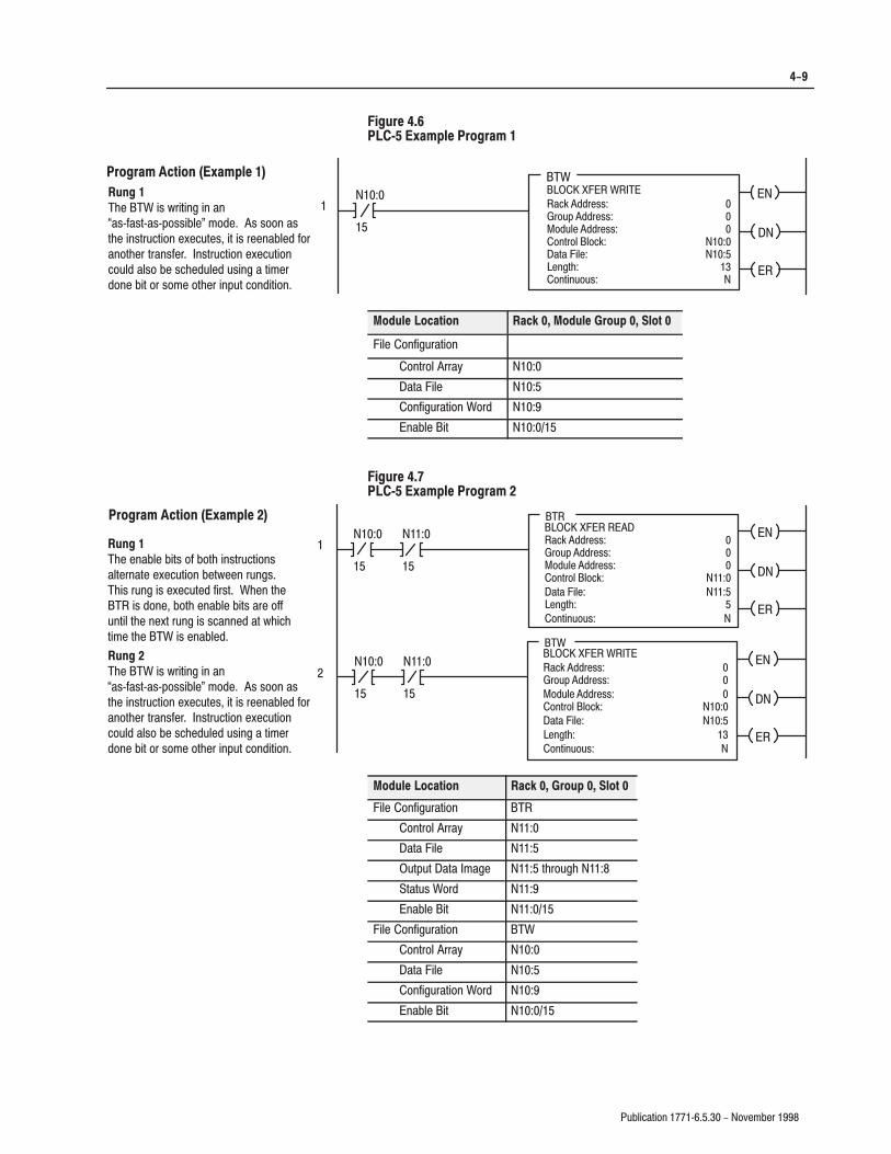
Output data is transferred from the processor’s data table to themodule with a write block transfer. Diagnostic information istransferred from the module to the processor’s data table with a readblock transfer. In order for these transfers to take place, you mustenter certain parameters into your block transfer instructions. Asample program segment with block transfer read and write is shownin Figure 4.1 and described in the following paragraphs.
An example program with block transfer instructions is shown inFigure 4.2. A data table map (Table 4.A) and a data table wordassignment (Table 4.B) are also shown. Figure 4.3 shows how thebinary representation of configuration options is represented in BCD(as it appears in our data table map).
���# �����
� �%� �����$ ������ � �� �� �" #�"# �
$
!,(+��25*1�#8(49-,8��54,��0: ":58(.,��0:
�
&80:,��25*1�#8(49-,8��54,��0: ":58(.,��0:
������'��!�&!�#�
�(:(��++8,99�
�5+;2,��++8,99�
�25*1��,4.:/�
�02,�
>>>
!�"
��
>>>�>>>
��":58(.,��0:
�4()2,
�
��
�54,
�
�����#���������%�
�5;4:,8��++8,99�
590:054�
�02,��,4.:/�
�02,���
>>>
>>>
>>>
>>>�>>>
��
�02,�!�
!(:,�6,8�"*(4�
>>>�>>>
>>>
!,(+��25*1�#8(49-,8��54,��0:�4()2,
�
��
�54,
������'��!�!���
�(:(��++8,99�
�5+;2,��++8,99�
�25*1��,4.:/�
�02,�
>>>
!�"
��
>>>�>>>
��
":58(.,��0:�4()2,
�
��
�54,
�
�
�
� �� �� �"���
�#��! � ��� �
#/, -089: :=5 8;4.9 5- :/, 9(362, 685.8(3 9,.3,4:
:5..2, 8,7;,9:9 -58 :/, 8,(+ (4+ =80:, 049:8;*:0549�
�5:0*, :/(: :/, �'����� �� 049:8;*:0549 04 !;4.9
(4+ (8, :/, +54, )0:9 5- :/, 8,(+ (4+ =80:,
049:8;*:0549� �? 2(:*/04. 58 ;42(:*/04. ( 9:58(., )0:�
:/, =80:, +54, )0: �'''�'�� :80..,89 :/, 8,(+ )25*1
:8(49-,8 049:8;*:054 (4+ :/, 8,(+ +54, )0: �'''�'��
:80..,89 :/, =80:, )25*1 :8(49-,8 049:8;*:054�
#/, =80:, )25*1 :8(49-,8 049:8;*:054 04 !;4. � 9,4+9
*54-0.;8(:054� 5;:6;:� (4+ 9*(204. +(:( :5 :/, 35+;2,
-853 :/, 685*,9958 04 54, 685.8(3 9*(4�
#/, 8,(+ )25*1 :8(49-,8 049:8;*:054 04 !;4. � 9,4+9
35+;2, 9:(:;9 04-583(:054 (4+ ( *56? 5- :/, 5;:6;: +(:(
:5 :/, 685*,9958 -853 :/, 35+;2, 04 54, 685.8(3 9*(4�
&/,4 ( 8,(+ )25*1 :8(49-,8 /(9 ),,4 9;**,99-;22?
*5362,:,+� 0:9 +54, )0: ��0: '''�'�� 09 9,:� &/,4 :/,
+54, )0: 09 9,:� 0: ,4()2,9 :/, -02,@:5@-02, 35<, 049:8;*:054�
#/, 8,(+ )25*1 :8(49-,8 +(:( -02, �);--,8� 09 :/,4 35<,+
04:5 ( 9:58(., +(:( -02,� #/09 68,<,4:9 :/, 685*,9958 -853
:8(4930::04. 04<(20+ +(:( 9/5;2+ ( )25*1 :8(49-,8
*533;40*(:054 -(;2: 5**;8�
�#�� �
�#�� �
�#�� �
$654 *5362,:054 5- ( 9;**,99-;2 8,(+ )25*1 :8(49-,8�
+(:( -853 :/, 35+;2, 09 35<,+ -853 :/, );--,8 -02,
�)25*1 :8(49-,8 8,(+ -02,� :5 ( 9:58(., +(:( -02,� #/09
68,<,4:9 :/, 685*,9958 -853 ;904. 04<(20+ +(:( 9/5;2+
)25*1 :8(49-,8 *533;40*(:0549 -(02�
�: 65=,8@;6� :/, 685.8(3 6,8-5839 ( =80:, )25*1
:8(49-,8 :/(: *54-0.;8,9 :/, 35+;2,� &/,4 :/, -089:
=80:, )25*1 :8(49-,8 09 *5362,:,� :/, 685.8(3 :5..2,9
),:=,,4 8,(+ (4+ =80:, )25*1 :8(49-,89� #/, 685.8(3
:(1,9 04:5 (**5;4: :/(: :/, 8,(+ (4+ =80:, 8,7;,9: )0:9
*(445: ), 9,: 903;2:(4,5;92?�
���� � ��!��
� �� ������ % � �%�
�����$ � ���!!� ! ���$

���
�9(1/)'8/43 ����; ���� � �4:+2(+6 ����
PLC-2 Family Example Program
�&�+#� �&��*!&% ���" �� �&�+#� �(&+' �� �#&* �
"�� �**6+77+7�� ,46 �14)0 "6'37,+6 %6/8+
�� ,46 �14)0 "6'37,+6 +'*
�"% �/1+ ��43,/-96'8/43 ,/1+� ���;���
�" �/1+ ��9,,+6 ,/1+� ���;���
�98598 �'8' �/1+ ����;����
!846'-+ �/8 ������
�"% �43+ �/8 �����
�" �43+ �/8 ���;��
�&�+#� �&%�! +(�*!&% ����.���� ��&#*� � ��()!&%�
$418'-+ '3-+ � 84 �$
�'8' �462'8 ���
!)'1/3- �'6'2+8+67
�.'33+17 � '3* � �4 7)'1/3-
�.'33+1 � ;� 84 ��
�.'33+1 � � ��� 84 ���
�! +(����
���. ��$!#- �,�$'#� �(& (�$
#
��
���
�
�
���
������&�� �% �"�
�'8'��**6+77�
�4*91+��**6+77�
�14)0��+3-8.�
�/1+�
��
���
��
�����
�����
��
���
�
��
���
�
�����"���������$�
�4938+6��**6+77�
�47/8/43�
�/1+��+3-8.�
�/1+���
���
���
���
�����
��
�/1+� �
'8+�5+6�!)'3�
�������
���
���
��
���
��
��
���
��
������&�� � ���
�'8'��**6+77�
�4*91+��**6+77�
�14)0��+3-8.�
�/1+�
��
���
��
�����
�����
��
���
��
��
���
��
��
��
���
���
� ������� �� �!"� "

����
�5%-,&$4,0/ � �8����� � �06(.%(2 ����
�� ������
���� �� �� ��
������������� �������� �� ����������
�$4$ $%-( ��� ����8702'�
��
��
��
�
�
��
��
�
��
��
��
�
�
��
��
�
��
��
��
�
�
��
��
�
�
�
�
�
�
�
�
�
�
�
��
��
��
�
�
��
��
�
��
��
��
�
�
��
��
�
�
�
�
� �� � ��
�� ��!����
�
������� ���
��"02'3��0��&$-,/*
� �� ����"�����������
��
������ �����
��������
��
��
��
�
�
��
��
�
��
��
��
��
��
�
�
��
��
�
��
��
��
�
�
��
��
�
��
��
��
�
�
��
��
�
�
�
�
�
�
�
�
�
�
�
��
��
��
�
� �� � ��
�� ��!����
������� ���
� �� ����"�����������
��
���������
�� �� �������#�
���� ��
������� �
OFE Data Table–Write Block PLC-2 Family
����
��702'3�",4+��&$-,/*
�0/),*52$4,0/�$4$
�� "�
� �� � ��
�� ��!����
������� ���
�/154��$4$�,-(����
� �� ����"�������������
�5))(2��2($� �

����
�.$('%#-'+* � �0����� � �+/&)$&, ����
��������
��#� ����" ��!� ����� ����
���������������������������!������
�� �� �����!������������� �����!����
!�������� ������� ��� !�������� ������� ���
�
�
�
�
�
�
�
�
�
�
�
�
�
�
�
�
�
�
�
�
�
�
�
�
�
�
�
�
�
�
�
�
�
�
�
�
�
�
�
�
�����������
�� �
������ �����
��������
���������
�� �� �������"�
OFE PROGRAM PLC-2 FAMILY & PLC-3
CH 1 DATA
CH 2 DATA
CH 3 DATA
CH 4 DATA
0100
0
4095
0
4095
20
275
100
500
2 2
�����! � Block length for block transfer write is 00. Unscaled channels have a minimum scalingvalue of 0 and a maximum scaling value of 4095. If channels 1 and 2 were configured for + 10V operation,then the minimum scaling value would be -4095 and the maximum scaling value wouldbe +4095. Since channel 3 has a negative minimum scaling value, you must set the polar-ity bit (bit 10) associated with channel 3’s minimum scaling word in the configurationword (word 5 of the write block).
�����

� � � �
�' ,,$* �(,(+2+ �" *(,& � "1-/ �-* /(14
�$1 ��� � �$& 1(3$
�$0$1 ��� � �-0(1(3$
�(, /4
���
���
����
�2!*(" 1(-, ����5 ���� � �-3$+!$/ ����
�'&1.$����
�'+!.2 �,+%'&1.!0',+ ,.# �$-.$/$+0$# '+ ���
,.#��$"� �'0 � � � �� �� �� �� � �� �� � � ��
,.#��"0!) �'0 � � � � � �� �� � �� �� � � ��
�-/# � � � � � � � � � � � � � � � � �
Block transfer operation with the PLC-3 processor uses one binaryfile in a data table section for module location and other related data.This is the block transfer control file. The block transfer data filestores data that you want transferred to your module (during blocktransfer write) or from your module (block transfer read). Theaddress of the block transfer data file is stored in the block transfercontrol file. A sample program segment is shown in Figure 4.4 anddescribed in the following paragraphs.
The industrial terminal prompts you to create a control file wheneither block transfer instruction is entered. The same block transfercontrol file is used for both read and write instructions for yourmodule.
PLC-3 Example Program
�,#1)$ �,"!0',+ �!"( � �,#1)$ �.,1- �� �),0
�*-") �/ ,0%$/ �-,1/-* �(*$ �����
��� �(*$ ��-,%(&2/ 1(-, %(*$� ����
��� �(*$ ��2%%$/ %(*$� ����
�21.21 � 1 �(*$ �����
�1-/ &$ �(1 ����
��� �-,$ �(1 �������
��� �-,$ �(1 �������
�,#1)$ �,+%'&1.!0',+ ��3��� ��,)0!&$ �$./',+�
�-*1 &$ � ,&$ � 1- ��
� 1 �-/+ 1 ���
�" *(,& � / +$1$/0
�' ,,$*0 � ,# � �- 0" *(,&
�' ,,$* � 5� 1- ��
�' ,,$* � � ��� 1- ���
�),"( �.!+/%$.
�.,&.!**'+& 3 ���3�
�!*')2 �.,"$//,./ �+)2

���
:(1/)'9/43 ��?�� ��� � �4;+2(+7 ���
����������
� � � ������ ������� ���������
������&��!�%!�#�
!')0��**77+88�
�74:5��**7+88�
�4*:1+��**7+88�
�'9'��**7+88�
===
=
======
=====�====
�+3-9.�
��#��
=
=====�====
$
!+'*��14)0�#7'38,+7��43+��/9 "947'-+��/9
�
%7/9+��14)0�#7'38,+7��43+��/9 "947'-+��/9
����"��!�����#��!
�/1+���
�/1+�!�
�4:39+7��**7+88�
48/9/43��+3-9.�
=====�====
=====�====
=====
��=
��
�4*+� �11�")'3
!+'*��14)0�#7'38,+7��43+��/9 �3'(1+
��
�43+
"947'-+��/9
�!
�7747
������&��!�!���
!')0��**7+88�
�74:5��**7+88�
�4*:1+��**7+88��'9'��**7+88�
===
=
===========�====
�+3-9.�
��#��
=
=====�====
��
�3'(1+
��
�43+
�!
�7747
�
"947'-+��/9 ��
�3'(1+
�
��
�43+
�
�!
�7747
��
�
�
�#%
�#!
����� � ��� �
#.+ ,/789 9<4 7:3-8 4, 9.+ 8'251+
574-7'2 8+-2+39 94--1+ 7+6:+898 ,47
9.+ 7+'* '3* <7/9+ /3897:)9/438� �49/)+
9.'9 9.+ �&����� �� /3897:)9/438 /3
!:3-8 '3* '7+ 9.+ *43+ (/98 4, 9.+
7+'* '3* <7/9+ /3897:)9/438� �> 1'9)./3-
47 :31'9)./3- ' 8947'-+ (/9� 9.+ <7/9+
*43+ (/9 �&&&&&�&&&&�� � 97/--+78 9.+
�#! /3897:)9/43 '3* 9.+ 7+'* *43+ (/9
�&&&&&�&&&&� � 97/--+78 9.+ �#%
/3897:)9/43�
���� �
#.+ <7/9+ (14)0 97'38,+7 /3897:)9/43 /3
!:3- � 8+3*8 )43,/-:7'9/43� 4:95:9� '3*
8)'1/3- *'9' 94 9.+ 24*:1+ ,742 9.+
574)+8847 /3 43+ 574-7'2 8)'3�
���� �
#.+ 7+'* (14)0 97'38,+7 /3897:)9/43 /3
!:3- � 8+3*8 24*:1+ 89'9:8
/3,472'9/43 '3* ' )45> 4, 9.+ 4:95:9
*'9' 94 9.+ 574)+8847 ,742 9.+ 24*:1+
/3 43+ 574-7'2 8)'3�
���� �
%.+3 ' 7+'* (14)0 97'38,+7 .'8 (++3
8:))+88,:11> )4251+9+*� /98 *43+ (/9 /8 8+9�
%.+3 9.+ *43+ (/9 �&&&&&�&&&&� � /8
8+9� /9 +3'(1+8 9.+ ,/1+?94?,/1+ 24;+
/3897:)9/43� #.+ 7+'* (14)0 97'38,+7 *'9'
,/1+ �(:,,+7� /8 9.+3 24;+* /394 ' 8947'-+
*'9' ,/1+� #./8 57+;+398 9.+ 574)+8847
,742 97'382/99/3- /3;'1/* *'9' 8.4:1* '
(14)0 97'38,+7 )422:3/)'9/43 ,':19 4)):7�
�9 54<+7?:5� 9.+ 574-7'2 5+7,4728 ' <7/9+ (14)0 97'38,+7 9.'9 )43,/-:7+8 9.+ 24*:1+� %.+3 9.+ ,/789 <7/9+ (14)0 97'38,+7 /8 )4251+9+� 9.+
574-7'2 94--1+8 (+9<++3 7+'* '3* <7/9+ (14)0 97'38,+78� #.+ 574-7'2 9'0+8 /394 '))4:39 9.'9 9.+ 7+'* '3* <7/9+ 7+6:+89 (/98 )'3349 (+ 8+9
8/2:19'3+4:81>�
$543 )4251+9/43 4, ' 8:))+88,:1 7+'* (14)0 97'38,+7� *'9' ,742 9.+ 24*:1+ /8 24;+* ,742 9.+ (:,,+7 ,/1+ �(14)0 97'38,+7 7+'* ,/1+� 94 ' 8947'-+
*'9' ,/1+� #./8 57+;+398 9.+ 24*:1+ ,742 :8/3- /3;'1/* *'9' 8.4:1* (14)0 97'38,+7 )422:3/)'9/438 ,'/1�
������� �����

����
�7'/-(&6-21 ����9����� � �28*0'*4 ���
���'$�����
���*� �(� #�� �$"�$�
#
�
�
�
����������
�����
��
��
��
�"
������%�� � ���
&(.��))4*55�
�4273��))4*55�
�2)7/*��))4*55�
�&6&��))4*55�
���
�
�����-+,
����������
�*1+6,�
��"��
�
����������
��
��"�
��
��
��"�
�
�
��"�
��
�����
��
�"$
������%�� �$ �"�
&(.��))4*55�
�4273��))4*55�
�2)7/*��))4*55�
�&6&��))4*55�
���
�
�����-+,
����������
�*1+6,�
��"��
�
����������
��
��"�
��
��
��"�
�
�
��"�
��
71+��70'*4� ��
71+��70'*4� ��
71+��70'*4� ��
71+��70'*4� ��
�����
�����
����������
���������
���*� �&� ����� �"$� %%��! �!&% �"$ �(� #�� �
!6&46 � ����������
$24) � � � � � � �
����� ���� �� ��� ��� ��� ���� ���� ��
���� ���� �� ���� ��� ���� ���
The PLC-5’s bidirectional program is very simple because theprocessor handles the enable bits and ensures valid data. Twoexamples are shown. The first is a write-only program you can usewhen module status is not required. The second is a read/writeprogram.
� #"$&�!& If the 1771-OFE module is configured in BCD dataformat and you are using a PLC-5 processor, extraprogramming will have to be added to the ladderprogram (i.e. a CPT or TOD instruction) to convertbinary data to BCD data before it is transferred to the1771-OFE module’s block transfer write data file. Also,when checking your program’s operation, remember toverify proper output voltage/current values based on thedata values sent to the module.
��"�� �$�!%��$
�$"�$� �!� * ���*�
�� ��) �$"��%%"$% �!�)
���
�6%.,&$5,10 � �<����� � �17(/%(3 ����
���'%����
���)� �(�!$ � �%#�%�! �
�����
��
�!"
������#����"��!�
�$&-��''3(44�
�3162��''3(44�
�1'6.(��''3(44�
�10531.��.1&-�
�
�
�
�����
�$5$��,.(�
�(0*5+�
�����
�
��
��
���105,06164� �
�
�'"� �
!+( �!" ,4 83,5,0* ,0 $0
;$4<)$45<$4<2144,%.(� /1'(� �4 4110 $4
5+( ,04536&5,10 (9(&65(4� ,5 ,4 3((0$%.(' )13
$015+(3 53$04)(3� �04536&5,10 (9(&65,10
&16.' $.41 %( 4&+('6.(' 64,0* $ 5,/(3
'10( %,5 13 41/( 15+(3 ,0265 &10',5,10�
�%#�%�! ��&�#" ��(�!$ � ��
�#�' � �#��&�#" ���� �� �#�' � �%#'$ �� � #& �
�,.( �10),*63$5,10
�10531. �33$: �����
�$5$ �,.( �����
�10),*63$5,10 "13' �����
�0$%.( �,5 ��������
���'%���
���)� �(�!$ � �%#�%�!
�����
��
�!�
������#��������
�$&-��''3(44�
�3162��''3(44�
�1'6.(��''3(44�
�10531.��.1&-�
�
�
�
�����
�$5$��,.(�
�(0*5+�
�����
�
��
��
���105,06164� �
�����
��
�����
��
�!"������#����"��!�
�$&-��''3(44�
�3162��''3(44�
�1'6.(��''3(44�
�10531.��.1&-�
�
�
�
�����
�$5$��,.(�
�(0*5+�
�����
�
��
��
���105,06164� �
�����
��
�
�%#�%�! ��&�#" ��(�!$ � �
�'"� �
!+( (0$%.( %,54 1) %15+ ,04536&5,104
$.5(30$5( (9(&65,10 %(58((0 360*4�
!+,4 360* ,4 (9(&65(' ),345� "+(0 5+(
�!� ,4 '10(� %15+ (0$%.( %,54 $3( 1))
605,. 5+( 0(95 360* ,4 4&$00(' $5 8+,&+
5,/( 5+( �!" ,4 (0$%.('�
�'"�
!+( �!" ,4 83,5,0* ,0 $0
;$4<)$45<$4<2144,%.(� /1'(� �4 4110 $4
5+( ,04536&5,10 (9(&65(4� ,5 ,4 3((0$%.(' )13
$015+(3 53$04)(3� �04536&5,10 (9(&65,10
&16.' $.41 %( 4&+('6.(' 64,0* $ 5,/(3
'10( %,5 13 41/( 15+(3 ,0265 &10',5,10�
�#�' � �#��&�#" ���� �� �%#'$ �� � #& �
�,.( �10),*63$5,10 �!�
�10531. �33$: �����
�$5$ �,.( �����
�65265 �$5$ �/$*( ����� 5+316*+ �����
5$564 "13' �����
�0$%.( �,5 ��������
�,.( �10),*63$5,10 �!"
�10531. �33$: �����
�$5$ �,.( �����
�10),*63$5,10 "13' �����
�0$%.( �,5 ��������

�����
���������� ��������� � �������� ���
When writing your program, there are some additional programmingtechniques that you should consider. They are:
• block length and scaling considerations
• block transfer boundary word - PLC-2 family processors
• module update time
• buffering data - PLC-2 family processors only
• system expansion recommendations
��� � ������ ��� � ����� ��������������
There are three possible write block configurations that involvescaling:
• no channels scaled
• fewer than four channels scaled
• all four channels scaled
No Channels Scaled
If you do not wish to scale any of your data, you can enter a blocklength of five words in the write block transfer instruction. The bitthat indicates BCD or 12-bit binary data format (Bit 17) in Word 5,the module configuration word, is the only bit in Word 5 that isexamined by the module. The remaining bits (00-16) are ignored bythe module because these bits indicate scaling value polarity and datapolarity. The module does not acknowledge negative data unlessscaling is used.
Fewer than Four Channels Scaled
To scale only one, two, or three of the four channels, enter a blocklength of 00 and enter the appropriate scaling values for the channelsto be scaled. You must enter 0 or -4095 for the minimum scalingvalue and +4095 for the maximum scaling value for any unscaledchannels, depending on the range selected.
���� ����������
��������������

�����
�0�(& �/&+* ��4�� ��� � �+1")�"- ���
All Four Channels Scaled
To scale all four channels, enter a block length of 00 and enter theappropriate scaling values for the four channels, as shown in thefollowing table.
�� ��# ���"��� ������ �!
�����# �� �� ����� �"� �
�+ �%�**"(.
� �("!
����
�4���
4 ��
�4� )��
�4 �)�
� �(+ ' �"*$/% +#
�+ � �(&*$ �*#+-)�/&+*
�"2"- /%�* �+0-
���
� �(+ ' �"*$/% +# ��
�,,-+,-&�/" � �(&*$ ��(0".
4��� �&*&)0) � �(&*$ ��(0" �*! ���� ��3&)0)
� �(&*$ ��(0" #+- �*. �("! �%�**"(�.�
�%�**"(. � �("!�4���
4 ��
�4� )��
�4 �)�
� �(+ ' �"*$/% +# ��
�,,-+,-&�/" � �(&*$ ��(0".
� �&*&)0) � �(&*$ ��(0" �*! ��� ��3&)0) � �(&*$
��(0" #+- �*. �("! �%�**"(.
�(( �+0- �%�**"(.
� �("!
����
�4���
4 ��
�4� )��
�4 �)�
� �(+ ' �"*$/% +# ��
�,,-+,-&�/" � �(&*$ ��(0".
����� � ��!�� ��#��� $ �� � % � %� �����$ � ���!!� ! ���$
The purpose of the boundary word is to tell the processor not tosearch for additional block transfer addresses.
You set the boundary word by entering one word (16 bits) of zeros inthe timer/counter accumulated value area of the data table, after theword containing the last block transfer module address.
For example, if the last block transfer data address in theaccumulated value area of the data table is 035, the block transferboundary word is addressed as 036. Figure 4.8 shows the data tablestructure and a sample GET/PUT instruction used to program a blocktransfer boundary word.

�����
�-�&$��,$)( ����0����� � �).!'�!* ���
���%"�����
�$� ����� �$"%�$%"� ��� ������ ��#$"%�$� � �&��!�� � " � ��
�"��#��" %���"' � "�
�������$*+,��&)�%��*�(+"!*���,��� *!++
���
���
���
��
�������+,��&)�%��*�(+"!*���,��� *!++
������� *!++�)"��&)�%��*�(+"!*��)-( �*/��
�������!#$(($(#�� *!++�")*��$'!*��)-(,!*��
� � � � � � � � � � � � � � � �
���
���
���
���
����
��
�&)�% �*�(+"!* �)-( �*/ �)* �(+,*-�,$)(
Timer/CounterAccumulated Values
Area

�����
�)�!���(�$# ����-���� � �$*�"��& � �
���$�� � ��#� ����
Update time is defined as the amount of time it takes for the outputmodule to receive a block transfer scan and update all outputchannels. Refer to Figure 4.9. The output module updates the fouroutput channels in:
• 8 milliseconds when BCD data format and scaling are used
• 1.6 milliseconds when binary data format and no scaling are used
Block transfer from the processor is inhibited during this time span.
���$!�����
���$�� �$# $# � ��#� ����
�
� � �
�
���
�����
� � �!$� �&�#'��& �#����(�� +��!�
)%��(� �' ���#� �$"%!�(�� �$& �
"�!!�'��$#�' +�(� ��� �#� '��!�#��
�� "�!!�'��$#�' +�(� ��#�&, �#� #$
'��!�#�
� � �!$� (&�#'��& �#��!��
If you plan to add more block transfer modules to your system atsome future date, we recommend that you reserve a few words in thefirst available time/counter value area of the data table for blocktransfer addresses. This eliminates the need to reconfigure your datatable.
In this chapter you learned how to write data to the module, the dataformats used for block transfer, special programming techniques, andwere given sample program examples.
�&"#�� �% ��"���
����������#���" ' � '�
�!���""�!" ���&
�� #�! �$���!&

�����
���������� ��������� � �������� ���

������ �
�+�#"��*"&% ����-����� � �&,�$��( ���
����� ����� �� ���� ����
In this chapter, you will read about:
�&( !%�&($�*!&% &% ��� '���
����"% ��*� �(&$ *!� �&�+#� � � � � � � � � � ���
Block transfer read (BTR) programming moves status and data fromthe module to the processor’s data table in one I/O scan. Theprocessor user program initiates the request to transfer data from themodule to the processor.
The transferred words contain module status, channel status andinput data from the module. The maximum BTR data file lengthrequired is five words.
�!�+(�����
�&(� �))!�%$�%* �&( �#&�" �(�%)��( ����
���!$�# �!* �� �� �� �� �� �� �� �� � � �� �� �� �� �� ��
��*�# �!* � � �� �� �� �� �� �� � � �� �� �� �� �� ��
�&(� � �!�%%�# � ��� �%'+* ��*�
� �!�%%�# � ��� �%'+* ��*�
� �!�%%�# � ��� �%'+* ��*�
�!�%%�# ��� �%'+* ��*�
�&*
+)��
���
��)�*��)�(,�� ��*� ��#"�
�$'&(*�%* The user program that uses the read block transfer mustmake sure that Bits 06 and 07 (the write enable and readenable request bits) of the MCB are not setsimultaneously.
� �* � !) � �'*�(
�&%*�!%)
����!%� ��*� �(&$ * �
�&�+#�

����
�3"+)#!2).- ��6�� ��� � �.4%,"%0 ���
��������
�"��� � ��!� ��"��� �� ���� � ��!�� ����
�� �������� �"!
� �"�� �"!���!� ��"���
�)21 ��6
���6���(!--%+ ��� )-/32 $!2!�
�)21 ��6
���6���(!--%+ ��� )-/32 $!2!�
��)21 ��6
���6���(!--%+ � ��� )-/32 $!2!�
��)21 ��6
���6���(!--%+ � ��� )-/32 $!2!�
�)21 ��6��
(%- 1%2� )-$)#!2% )-4!+)$ #(!--%+ $!2! )1 1%-2 2. 2(% ,.$3+%�
�(%1% ")21 !0% -.2 0%1%2 3-2)+ ! #.00%#2 50)2% "+.#* 20!-1&%0 )1
1%-2� �)2 �� #.00%1/.-$1 2. �(!--%+ � �)2 � 2. �(!--%+ �
!-$ 1. .-�
�)21 ��6�
���6 ��%1%04%$
�)2 � ���
�1 2(% ��� ����� ")2� (%- 1%2� )2 )-$)#!2%1 2(!2 2(% /0.#%11.0
)1 )- ���� .0 ������� ,.$% �)�%�� "+.#* 20!-1&%0 $!2! )1 -.2
"%)-' 50)22%- 2. 2(% ,.$3+%��
The first four words of the block transfer read show the actual 12 bitsof data sent to the module’s digital to analog converters (DACs).The first four words in the block transfer read appear in 12-bit binaryformat regardless of the module’s mode of operation (BCD or 12-bitbinary).
The fifth word contains the status of each DAC word; that is,whether data is out of range or scaling is improperly programmed.The fifth word also indicates that I/O RESET has been established(when the processor is in the PROG/TEST or RUN mode).
In this chapter, you learned the meaning of the status data the modulesends to the processor.
����"� �#��� $

������ �
#<+31,*;165 ����B���� � !6=.4+.9 ����
��������� ���� �����������
In this chapter, you will read how to calibrate your output module.
� ���� ��"��� �� ��� ����
&663: *5- ;.:; .8<174.5; ����
�*31+9*;15/ @6<9 46-<3. ����
'63;*/. "<;7<; =.9:165 �����B"���� ���
�<99.5; "<;7<; =.9:165 �����B"�� � ����
�<99.5; "<;7<; =.9:165 �����B"���� ����
Table 6.A lists tools and test equipment required for modulecalibration.
��������
�!" ��#�����"
�!�� ��� ��#�����" ��!� ��"���
'63;*/. '.9:165:�B� �1/1; '63;4.;.9 ���� �,,<9*,@ 1514<4
'63;*/. '.9:165:� �6*- $.:1:;69: ��� 69 �9.*;.9� � �(� ��� �#! � � ��B���
�<99.5; '.9:165: � �6*- $.:1:;69: �� 604 69 �9.*;.9� � �(� ���� �#! ������B���
�6;0 '63;*/. *5- �<99.5;
%4*33 �.>.3.9�: %,9.>-91=.9
69
A#6; &>..2.9� �31/54.5; &663
!.>*92 �3.,;9651,:
��� !69;0 #<3*:21 $6*-
�01,*/6� �� ��� �
�*,273*5. �?;.5-.9 �*9- �*; !6 ����B�)
The analog output module is shipped from the factory alreadycalibrated. If it becomes necessary to recalibrate the analog outputmodule, you must calibrate it in an I/O chassis. The module needs tocommunicate with the processor. Calibration consists of two tasks:• preparing the module for calibration
• calibrating each channel
The calibration procedure for the voltage output version module isdifferent from the calibration procedure for the current outputversion module. Refer to the appropriate section for your module.
!ATTENTION: Do not attempt calibration withoutreading and thoroughly understanding all steps in thisprocedure. Also, do not attempt to calibrate thismodule in an operating system.
����"� �����"�$�!
���! ��� �!" ��#�����"
����� �"��� ��# ��#��

��
����
���������� ��������� � �������� ���
�!� �!�#��� ��! �����!�#��� �
1. Turn off the processor and I/O chassis power.
2. Remove the field wiring arm.
3. Remove the analog output module from the I/O chassis.
4. Remove the module covers.
5. Connect the backplane extender card (cat. no. 1771-EX) to thecircuit board.
6. Insert the extender card/circuit board assembly in the I/O chassis.
7. Reinstall the field wiring arm.
�� �!#��# If you have a spare or unused field wiring arm, you maywant to temporarily switch it with the module’s presentfield wiring arm. You can use this spare arm for testpurposes in order to avoid disconnecting your analogdevice wires.
�� �!#��# The accuracy of this calibration procedure is dependentupon the precision of your load resistors. Use resistorswith a tolerance of 1.0%. You should be able to attainvoltage readings to +1mV. For greater accuracy, useload resistors with tolerances less than 1.0%.
Use load resistors with values of 1K ohms. For greater accuracy,you can substitute the 1K ohm resistor with a resistor that moreclosely approximates your actual device load.
�����!�#��� �!����$!�
1. Disconnect your analog device wires from the module’s fieldwiring arm if you are not using a spare field wiring arm forcalibration.
2. Attach a resistor with a value of 1K or greater (to approximateyour actual load) across Channel 1 (the top two screws inFigure 6.1) of the field wiring arm.
3. Attach three more 1K resistors across the remaining threechannels on the field wiring arm just as you did in Step 2(Figure 6.1).
4. Place the LAST STATE configuration jumpers (Figure 6.2) in theMAX position (if they are not there already).
5. Select the +10V output range by placing the four channelconfiguration jumpers in the position shown in Figure 6.2.
���#��� �$# $# ��!"���
�����%� ���

����
�-�$#��,#'& ����1���� � �'.�%��* � �
6. Connect the voltmeter leads across the top two screws on the fieldwiring arm (Channel 1). The top screw is positive, and thesecond (lower) screw is negative.
7. Turn on the processor, I/O chassis, and the industrial terminal.
���"������
�� � !�� ��������! �� ����� ������ ���
�
�
�
�
�
�
�
�
�"�&&�$ �
�"�&&�$ �
�"�&&�$ �
�"�&&�$ �
�#�$� �#*#&! �*%
�� '* !*��,�*
*�+#+,'*+
��� �
���"������
��� ���� �����"��!��� �"����
�*'&,
'
�'�-$�
�*#&,�� �#*�-#, �'�*� �'( �#�/
�#� ��0�'$� $�+, +,�,� �#&
�'+#,#'& ($-!+ �+ *�)-#*���
LAST STATE
�� ��1�

��
�
��
����
�.�&$��-$)( ����1 ���� � �)/ '� + ����
�� ������
�������� �� ������ ������ � ����� ��� �������� ����
�������
��
�
��
�
��
�
��
�
��
�
��
����
���
� ,$,-)+ �)- (-$)' - +,
��%.,-' (- ��+ 0,
�)(!$".+�-$)( �.'* +,
�, - !)+ ���� ,��& �
���� �����
���
� � �
�����
��� ���
��� ���
�#�(( & �
�#�(( & �
�#�(( &
�#�(( &
8. Place the processor in the TEST or PROG mode.
9. Output full scale (+10V) either with write block transfer data orby placing the LAST STATE configuration jumpers in the MAXposition.
10.Adjust R66 until the reading is 10V +1mV.
11.Output -10V either with write block transfer data or by placingthe LAST STATE configuration jumpers in the MIN position.
12.Adjust R67 until the reading is one-half the difference between-10V and the initial reading.
13.Output full scale (+10V) again, either with write block transferdata or by placing the LAST STATE configuration jumpers in theMAX position.
14.Adjust R66 again until the reading is 10V +1mV.
���
����������� ���������� � �������� ���
15.Reconnect the voltmeter to the appropriate screws on the fieldwiring arm. Repeat Steps 9 through 14 for Channels 2, 3, and 4,until you obtain the desired tolerance. Table 6.B lists theappropriate resistor pots for each channel.
��������
����� �� �� �
������� ����� �� �� �
� ���� ���
� ���� ��
� � �� � �
� �� �
16.Turn off power to the module.
17.Return the LAST STATE configuration jumpers to the positionthey were in before you started calibration.
18.Return the channel configuration jumpers to their originalpositions.
19.Remove the extender card and return the circuit board to themodule.
20.Replace the module covers.
21.Return the module to the I/O rack.
22.Replace your analog device wires (or the original field wiringarm if you used a spare for calibration purposes).
Your module should now be properly calibrated and ready for use.
������� ��� ��� ������� ���
1. Turn off the processor and I/O chassis power.
2. Remove the analog output module from the I/O chassis.
3. Remove the module covers.
4. Connect the backplane extender card (cat no. 1771-EX) to thecircuit board.
5. Insert the extender card/circuit board assembly in the I/O chassis.
6. Reconnect the field wiring arm.
�!���� �! �! �������
���"�� ��

����
�#�����"��� ����%���� � ��$���� � �
������� �����������
1. Disconnect your analog device wires from the module’s fieldwiring arm.
��������� If you have a spare or unused field wiring arm, you maywant to temporarily switch it with the module’s presentfield wiring arm. You can use this spare arm for testpurposes in order to avoid disconnecting your analogdevice wires.
��������� The accuracy of this calibration procedure is dependentupon the precision of your load resistors. We suggestusing resistors with a tolerance of 0.01%. You shouldbe able to attain voltage readings to +2mV. (If you useresistors of a value different from 250 ohms, you shouldbe able to attain voltage readings of +0.05% of V out.)If you require greater accuracy, you need to use loadresistors with tolerances less than 0.01%.
Use load resistors with values of 250 ohms. For greater accuracy,you can use a resistor that more closely approximates your actualdevice load.
2. Attach a resistor with a value of 250 ohms across Channel 1 (thetop two screws) of the field wiring arm.
3. Attach three more 250 ohm resistors across the remaining threechannels on the field wiring arm just as you did in step 2(Figure 6.4).
���������
�������� ��������� �� ���� ����� ���
�
�
�
�
�
�
�
�
������� �
������� �
������� �
������� �
������
�!�!"� !
�� ������ �� ��� � �
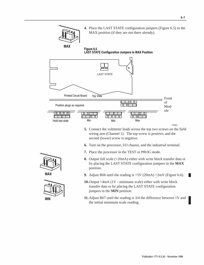
���
FrontofMod-ule
�"��$�� �"�%�$ ���"� �� ���'
��� ��(���� ��#$ #$�$� ���
��#�$��� �%�# �# "�!%�"���
�����)�
���
���
����
�%�����$��� ��)������ � ��&����" ���
4. Place the LAST STATE configuration jumpers (Figure 6.5) in theMAX position (if they are not there already).
�� ������
��� ���� ������ ������ � ����� �� ��� ��������
LAST STATE
5. Connect the voltmeter leads across the top two screws on the fieldwiring arm (Channel 1). The top screw is positive, and thesecond (lower) screw is negative.
6. Turn on the processor, I/O chassis, and the industrial terminal.
7. Place the processor in the TEST or PROG mode.
8. Output full scale (+20mA) either with write block transfer data orby placing the LAST STATE configuration jumpers in the MAXposition.
9. Adjust R66 until the reading is +5V (20mA) +2mV (Figure 6.6).
10.Output +4mA (1V - minimum scale) either with write blocktransfer data or by placing the LAST STATE configurationjumpers in the MIN position.
11.Adjust R67 until the reading is 3/4 the difference between 1V andthe initial minimum scale reading.

��
����
�/�'%��.%*) ��2�� ��� � �*0!(�!, ���
����������
������� �� �������� ����
�������
��
�
��
��
�
�
��
�
��
�
��
���
��
�!-%-.*, �*.!).%*(!.!,-
� &/-.(!). ��,!1-
�*)"%#/,�.%*) �/(+!,-
�-!. "*, ��� -��'!�
���� �����
���
��� ���
������
�� ���
��� ���
�$�))!' �
�$�))!'
�$�))!'
�$�))!' �
12.Output full scale (+20mA) again, either with write block transferdata or by placing the LAST STATE configuration jumpers in theMAX position.
13.Adjust R66 until the reading is 5V +2mV.
14.Reconnect the voltmeter to the appropriate screws on the fieldwiring arm. Repeat Steps 8 through 13 for Channels 2, 3, and 4until the desired tolerance is obtained. Table 6.C lists theappropriate resistor pots.
��������
�������� ����
������� �������� ����
���� ���
���� ���
� ���� ��
� ���� ���

���
���������� ��������� � �������� ���
15.Remove the extender card and return the circuit board to themodule.
16.Replace the LAST STATE configuration jumpers to their originalposition.
17.Replace the module covers.
18.Return the module to the I/O rack.
19.Replace your analog device wires (or the original field wiringarm if you used a spare for calibration procedures).
Your module should now be properly calibrated and ready for use.
����������� ��� �����������
1. Turn off power to the processor and I/O chassis.
2. Remove the analog output module from the I/O chassis.
3. Remove the module covers.
4. Connect the backplane extender card (cat. no. 1771-EX) to thecircuit board and insert the extender card into the I/O chassis.
5. Reconnect the wiring arm to the circuit board.
������� �����������
1. Disconnect your analog device wiring from the module’s wiringarm.
��������� If you have a spare or unused field wiring arm, you maywant to temporarily switch it with the module’s presentwiring arm. Use the spare wiring arm for test andcalibration purposes to eliminate disconnecting yourdevice wiring.
��������� The accuracy of this calibration procedure depends onthe precision of the load resistors used. Use resistorswith a tolerance of 0.01%. You should be able to obtainvoltage readings to +5mV. (If you use resistors of avalue different from 250 ohms, you should be able toobtain voltage readings of +0.05% of V out). If yourequire greater accuracy, use load resistors withtolerances less than 0.01%.
If greater accuracy is required, substitute resistors that moreclosely approximate your actual device load.
� ����� � �� � �������
�����!� ���

��
�����
�#�����"��� ����%���� � ��$���� � �
2. Attach 250 ohm resistor across Channel 1 (the top two screws) onthe field wiring arm.
���������
�������� ��������� �� ���� ����� ���
�
�
�
�
�
�
�
�
������� �
������� �
������� �
������� �
������
�!�!"� !
�� ������ �� ��� � �
3. Attach three more 250 ohm resistors across Channels 2, 3, and 4(Figure 6.7).
4. Place the LAST STATE configuration jumpers in the MAXposition (if they are not there already).
5. Connect a voltmeter across the top two screws on the field wiringarm (top screw is positive, and second screw is negative).
6. Turn processor, I/O chassis, and industrial terminal ON.
7. Place processor in the TEST or PROG mode.
8. Output full scale (+50mA) with write block transfer data.
9. Adjust R66 (Figure 6.6) until the reading is +12.5V (50mA)+5mV.
10.Repeat steps 8 and 9 for channels 2, 3 and 4. Adjust as necessaryuntil the desired tolerance is obtained. Associated resistorpotentiometers are shown in Table 6.D.
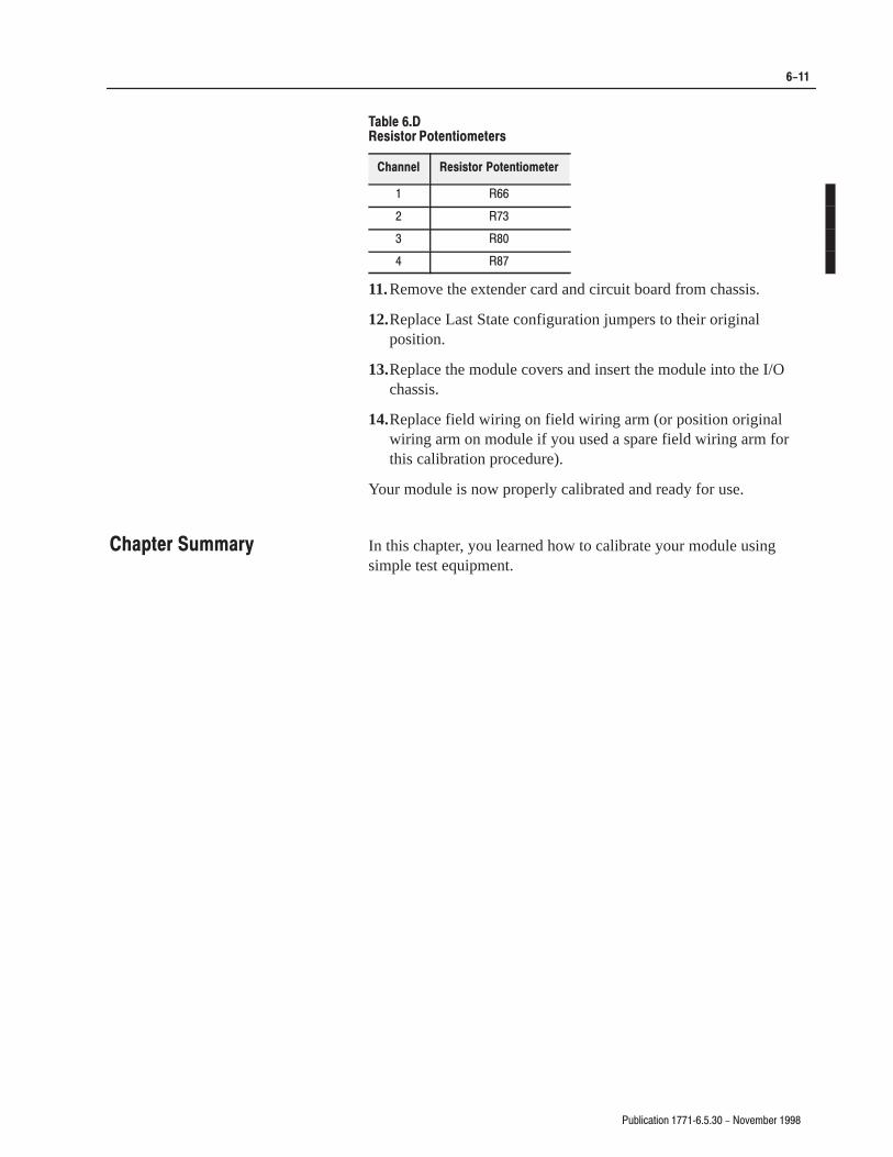
�����
����������� ��������� � �������� � �
�� ������
������� ��������������
������� ������� �������������
� �
� ���
� ���
� ���
11.Remove the extender card and circuit board from chassis.
12.Replace Last State configuration jumpers to their originalposition.
13.Replace the module covers and insert the module into the I/Ochassis.
14.Replace field wiring on field wiring arm (or position originalwiring arm on module if you used a spare field wiring arm forthis calibration procedure).
Your module is now properly calibrated and ready for use.
In this chapter, you learned how to calibrate your module usingsimple test equipment.
������� ������

�����
���������� ��������� � �������� ���

������ �
�.�&$��-$)( � �1����� � �)/ '� + ����
��� ������ � �������������
In this chapter, you will read how to troubleshoot your outputmodule using indicator lights and diagnostic bits.
��� ����������� �� ��� ����
�(- +*+ -$(" -# $(�$��-)+ &$"#-, � � � � � � � � � � � � � � � � � � � � � � � � ��
� �� �&)�% �+�(,! + 0)+�, � � � � � � � � � � � � � � � � � � � � � � � � � � ��
The front panel of the module contains a green RUN and a red FLT(fault) indicator (Figure 7.1). At power-up, the red FLT indicatorlights and remains ON during an initial module self-check . If a faultis found initially or occurs later, the red FLT indicator stays lit. If afault is not found, the red indicator will turn off and the green RUNindicator will turn on and remain on. Possible module fault causesand corrective actions are shown in Table 7.A.
����������
���������� ����������
������
���
��� ����
���
���
� ��
������� ��������
������������ ��� ���������
�����

����
�3"+)#!2).- ����7����� � �.4%,"%0 ���
���%�����
�*(-�%�+"((,#'! �"�*,
�('�#,#(' �(++#�%� ��-+� ���(&&�'��� ��,#('
�0%%- ��� )-$)#!2.0 $.%1 -.2
#.,% .-�
�. �.5%0 2. �.$3+%
�!$ )-2%0-!+ &31%
• �(%#* ��� #(!11)1 &.0 /.5%0�
• �30- .&& /.5%0 2. ��� #(!11)1� �%,.4%
!-$ 0%)-1%02 ,.$3+% )-2. #(!11)1� �%230-
/.5%0 2. ��� #(!11)1�
�%$ ����� )-$)#!2.0 )1 .-
#.-2)-3.31+6 5)2( 2(%
/0.#%11.0 )- /0.'0!, !-$
03- ,.$%1�
�-13##%11&3+ �.5%07�/
• ����� �!3+2
• �(%#*13, �00.0
• �6#+% /.5%0�
• �%/+!#% &!3+26 ,.$3+% )& -%#%11!06�
�+.#* 20!-1&%01 !0% -.2 "%)-'
/%0&.0,%$�
• �+.#* �0!-1&%0
�-1203#2).-1 �0.'0!,,%$
�-#.00%#2+6
• �.$3+% (!1 &!)+%$
1%+&7$)!'-.12)#1�
• �(%#* 31%0 /0.'0!, �
• �6#+% /.5%0�
• �%/+!#% &!3+26 ,.$3+% )& -%#%11!06�
The module allows a five-word read block transfer for rudimentaryprogram or hardware debugging (Figure 7.2). If a read blocktransfer request is for more or less than five words, the module willnot perform a read block transfer.
�#!-*�����
�(*� �++#!'&�', (* ���� �%(�$ �*�'+ �*
���#&�% �#, � �� �� �� �� �� � �� �� � � �� �� �� �� ��
��,�% �#, �� � � �� �� �� �� �� �� � � �� �� �� �� ��
.0$ � �(!--%+ � ��� �-/32 �!2!
� �(!--%+ � ��� �-/32 �!2!
� �(!--%+ � ��� �-/32 �!2!
�(!--%+ ��� �-/32 �!2!
�.2
31%$
���
�%1%2�%1%04%$ �!2! �!+)$
�&)(*,�',� The user program that utilizes the read block transfermust make sure that bits 06 and 07 (the write enableand read enable request bits) of the MCB are not setsimultaneously.
The first four words of the read block transfer show the actual 12 bitsof data sent to the module’s digital-to-analog converters (DACs).The first four words in the read block transfer appear in 12-bit binaryformat regardless of the module’s mode of operation (BCD or 12-bitbinary).
���� �%(�$ �*�'+ �*
�,�,-+ �(*�+

����
�2!*(" 1(-, ��5�� ��� � �-3$+!$/ ���
The fifth word contains the status of each DAC word; that is,whether data is out of range or scaling is improperly programmed.The fifth word also indicates that I/O RESET has been established(when the processor is in the PROG/TEST or RUN mode).
��� ���� � ���������
�(10 ��5��
�'$, 0$1� (,#(" 1$ (,3 *(# "' ,,$* # 1 (0 0$,1 1- 1'$ +-#2*$�
�'$0$ !(10 /$ ,-1 /$0$1 2,1(* "-//$"1 4/(1$ !*-") 1/ ,0%$/ (0
0$,1� �(1 �� "-//$0.-,#0 1- �' ,,$* �� �(1 � 1- �' ,,$* ��
,# 0- -,�
�(1 �
�0 1'$ ��� ����� !(1� �'$, 0$1� (1 (,#(" 1$0 1' 1 1'$ ./-"$00-/
(0 (, ���� -/ ������� +-#$ �(�$�� !*-") 1/ ,0%$/ # 1 (0 ,-1
!$(,& 4/(11$, 1- 1'$ +-#2*$��
In this chapter you learned how to use the indicator lights and word 5in the BTR for troubleshooting your module.
���� � ������

����
���������� ��������� � �������� ���

������ �
"<+42,*;276 ����A���� � 7=.5+.9 ����
���������
!<;8<;: 8.9 �7-<4. � �6-2=2-<*44@ �:74*;.-
�7-<4. �7,*;276 �<44.;26 ���� �! �1*::2: � !6. $47;
!<;8<; '74;*0. #*60.: � 7526*4� �
����A!���
�� ;7 ��' ��
�� ;7 ��' ��
;7 ��' ��
!<;8<; �<99.6; �5*?25<5� �5� 8.9 �1*66.4 26 '74;*0. �7-. ������!����
!<;8<; �<99.6; #*60.: � 7526*4� �� ;7 ��5� ������!����
;7 ��5� ������!�� �
�202;*4 #.:74<;276 ��A�2; �26*9@ � � "*9; 26 ���
!<;8<; �*8*,2;*6,. ��µ� �'74;*0. !<;8<;:����µ� ��<99.6; !<;8<;:�
!<;8<; �58.-*6,. ���� 715: /79 '74;*0. !<;8<;: �?,4<:2=. 7/
�76;*,; (29260 #.:2:;*6,.
���� 5.0715: /79 �<99.6; !<;8<;:
�*? �778 �58.-*6,. 26 ;1. �<99.6; �7-. ����A!��� � &8 ;7 �� 715: �7*- #.:2:;*6,.
����A!�� � &8 ;7 � 715: �7*- #.:2:;*6,.
!<;8<; !=.947*- "97;.,;276 �44 7<;8<;: *9. 897;.,;.- *0*26:; :179; ,29,<2; 47*-
,76-2;276: 67; ;7 .?,..- 76. 526<;.�
�*,384*6. "7>.9 ����A!��� ����
����A!��� ����
����A!�� ����
"7>.9 �2::28*;276 ����A!��� ���(
����A!��� ���(
����A!�� � ��(
%1.95*4 �2::28*;276 ����A!��� ���� �%&19
����A!��� ���� �%&19
����A!�� ���� �%&19
�:74*;276 �' 95: �.;>..6 !<;8<; �1*66.4:
%.:;.- *; ��' �%9*6:2.6;� /79 �: �.;>..6 ;1.
!<;8<; �29,<2; *6- ;1. �76;974 �702, �$@:;.5
$2-.�
�� �76=.9;.9 $8.,2/2,*;276: $.;;4260 %25. �� 5: �*?25<5 /79 * #.:2:;2=. �7*-
�6;.96*4 $,*6 #*;. �� 5: /79 �44 �1*66.4: &:260 ��� �*;* *6-
$,*4260
��� 5: /79 �44 �1*66.4: &:260 �26*9@ �*;* *6- 7
$,*4260
�,,<9*,@ ��6,4<-260 �26.*92;@� �*26� *6-
!//:.; *; ��7��
���� 7/ �<44 $,*4.
��� �$� ���� �7-.�
��� �$� ��� �#) �7-.�
%.58.9*;<9. �7.//2,2.6; �� 8857� 7/ �<44 $,*4. #*60.
��������� ������ � ��� ����

����
9'0.(&8.32 ��>����� � �3:*1'*6 ���
�2:.6321*28&0 �32).8.327
�4*6&8.32&0 #*14*6&896*�
"836&,* #*14*6&896*�
�91.).8< !&8.2,�
3� 83 ��3� ����3� 83 � 3��
� 3� 83 ���3� �� 3� 83 ���3��
�� 83 ��� ��32��32)*27.2,�
�.*0) %.6.2, �61 �&8&03, �3� ��>%�
�.*0) %.6.2, �61 "(6*; #3659* �>� 4392)>.2(-*7 ������1�
�,*2(< �*68.+.(&8.32
�;-*2 463)9(8 36 4&(/&,.2, .7 1&6/*)�
• �"� (*68.+.*)
• �"� �0&77 �� �.:.7.32 �� �63947 �� �� �� �
(*68.+.*) �&=&6)397 36 232>-&=&6)397 03(&8.327
• $� 0.78*)
• $� �0&77 �� �.:.7.32 �� �63947 �� �� �� �
(*68.+.*) �&=&6)397 36 232>-&=&6)397 03(&8.327
• �� 1&6/*) +36 &00 &440.(&'0* ).6*(8.:*7

�������� �
���������� ��������� � �������� ���
��� � �������� ���� ����������� ������� �� ������
Programming multiple GET instructions is similar to block formatinstructions programmed for other PLC-2 family processors. Thedata table maps are identical, and the way information is addressedand stored in processor memory is the same. The only difference isin how you set up block transfer write instructions in your program.
For multiple GET instructions, individual rungs of ladder logic areused instead of a single rung with a block transfer instruction. Asample rung using multiple GET instructions is shown in Figure B.1and described in the following paragraphs.
��� �
This rung is used to set four conditions:
• EXAMINE ON Instruction (113/02) - This is an optionalinstruction. When used, block transfers will only be initiatedwhen a certain action takes place. If you do not use thisinstruction, block transfers will be initiated every I/O scan.
• First GET Instruction (030/120) - Identifies the module’s physicaladdress (120) by rack, group, and slot and where in theaccumulated area of the data table this data is to be stored (030).
• Second GET Instruction (130/060) - Indicates the address of thefirst word of the file (060) to which or from which the data istransferred. The file address is stored in Word 130, 1008 abovethe data address.
• OUTPUT ENERGIZE Instruction (012/07) - Enables the blocktransfer read operation. If all conditions of the rung are true, theblock transfer read enable bit (07) is set in the output image datatable control byte. The output image table control byte containsthe read enable bit and the number of words to be transferred.The OUTPUT ENERGIZE instruction is defined as follows:
• “0” indicates that it is an output instruction.• “1” indicates the I/O rack address.• “2” indicates the module group location within the rack.• “07” indicates that the module is in the lower slot and that this
is a block transfer read operation (if this were a block transferwrite operation, “07” would be replaced by “06”).
��������� The OUTPUT ENERGIZE Address 012/07 in thisexample indicates that the module is in Slot 0. Theaddress could be 012/17, which indicates that themodule is in Slot 1 (012/06 or 012/16 for a writeoperation).
�������� �� ������������

���
�2!*(" 1(-, ����5���� � �-3$+!$/ ���
�!��� � ��� �
These OUTPUT ENERGIZE instructions (012/01 and 012/02)define the number of words to be transferred. This is accomplishedby setting a binary bit pattern in the module’s output image tablecontrol byte. The binary bit pattern used (Bits 01 and 02 energized)is equivalent to six words or channels and is expressed as 110 inbinary notation.
�!�� �!����"
Once the block transfer read operation is complete, the processorautomatically sets Bit 07 in the input image table status byte andstores the block length of the data transferred.
���!�����
�!� ���� �� ��� �!� ����
� 1 � !*$ ��
�
�
�-,1/-*
�41$
���
���
���
���
��
���
��
���
���
���
��
�21.21 �+ &$ � !*$ �-,1/-*
�41$ �-,1 (,0 �$ #
�, !*$ �(1 ,# �*-")
�$,&1' (, �(, /4 �-#$
� 1 �##/$00�-,1 (,0 �-#2*$
�##/$00 (, ���
�,.21 �+ &$ � !*$
�1 120 �41$
�-,1 (,0 �-,$ �(1
�1-/ &$ �-" 1(-,
�-,1 (,0 �(*$
�##/$00 (, ���
� ���� �� �
� � �
��
�
�
�1 120
�41$
� � �
�21.21
�+ &$ � !*$
�(+$/��-2,1$/
�""2+2* 1$#
� *2$0 �/$
�,.21
�+ &$
� !*$
�(+$/��-2,1$/�/$0$1� *2$0 �/$
�(/01 �##/$00�
�$01(, 1(-, -%
�/ ,0%$//$# � 1
12994
��
��
�����
���
��
���
��
��
���
��
���
��
�
�

���
�/�'%��.%*) ����2���� � �*0!(�!, � �
The output module is capable of transferring up to 13 words in oneprogram scan. The number of words transferred is determined by theblock length entered in the output image table control byte.
The bits in the output image table control byte (Bits 00-05) must beprogrammed to specify a binary value equal to the number of wordsto be transferred.
For example, Figure B.2 shows if your output module is set up totransfer five words, you would set Bits 00 and 02 of the lower outputimage table control byte. The binary equivalent of five words, asstated in the look-up table, is 000101.
�!�+(�����
��**!%� �#&�" ��%�*
��.� � ,!--
�*).�%)- �* /'!
� ,!-- %) ���
�/.+/. �(�#! ���'! �*).,*'
�1.! �*).�%)- �!�
�)��'! �%. �) �'*�&
�!)#.$ %) �%)�,1 �* !
���
���
���
���
���� � �
��.� ���'!
�
�
�*).,*'�1.!
�!� �*, -
",*( �* /'!
�'*�& �,�)-"!,
�!� �)��'! �%.
�*, �'*�&
�,�)-"!, ��.%0!
�+!,�.%*)- �)'1
�/.+/. �(�#! ���'!
��
� � � � � � � �
�!%�(-��!*���**�(%
�&,�(��+*'+*��$�������#���-*�
�� � � �� �� ��
� � � � � ��!"�/'.
� � � � � ��
� � � � � ��
� � � � � ��
� � � � � ��
� � � � � �
� � � � � �
� � � � � ���
�+$��(�&�
�&(�)
*&��(�%)��(
��**!%� * � �#&�" ��%�*
��+#*!'#� � � �%)*(+�*!&%)
�%#-�

����
���������� ��������� � �������� ���

������ �
����������� �������� � �������� ����
���� ���� ��� ���
The 4-digit BCD format uses an arrangement of 16 binary digits torepresent a 4-digit decimal number from 0000 to 9999 (Figure C.1).The BCD format is used when the input values are to be displayedfor operator viewing. Each group of four binary digits is used torepresent a number from 0 to 9. The place values for each group ofdigits are 20, 21, 22 and 23 (Table C.A). The decimal equivalent for agroup of four binary digits is determined by multiplying the binarydigit by its corresponding place value and adding these numbers.
���������
������ ������ �� � ������
� � �� �
� � �� �
� � �� �
� � �� �
� � �� �
� � �� �
� � �� �
� � �� �
� � �� �
� � �� �
� � �� �
� � �� �
� � �� �
� � �� �
� � �� �
� � �� �
� � � � � � � � � � � � � � � �
�
�
�
���
� � � �
�������
������ ������ �� �
������ ����

����
����������� ��������� � �������� � �
���������
�� ��!#�$��%�%� �
����� ���&�
� ��� �� �� �� ��� �� ���
�������
�"&�'����%
� � � � �
� � � � �
� � � � �
� � � � �
� � � � �
� � � �
� � � �
� � � � �
� � � � �
� � � �
Signed-magnitude binary is a means of communicating numbers toyour processsor. It should be used with the PLC-2 family whenperforming computations in the processor. It cannot be used tomanipulate binary 12-bit values or negative values.
Example: The following binary number is equal to decimal 22.
101102 = 2210
The signed-magnitude method places an extra bit (sign bit) in theleft-most position and lets this bit determine whether the number ispositive or negative. The number is positive if the sign bit is 0 andnegative if the sign bit is 1. Using the signed magnitude method:
0 10110 = +221 10110 = -22
������)�����%&�� ���#(

����
���������� ��������� � �������� ���
Two’s complement binary is used with PLC-3 processors whenperforming mathematical calculations internal to the processor. Tocomplement a number means to change it to a negative number. Forexample, the following binary number is equal to decimal 22.
101102 = 2210
First, the two’s complement method places an extra bit (sign bit) inthe left-most position, and lets this bit determine whether the numberis positive or negative. The number is positive if the sign bit is 0 andnegative if the sign bit is 1. Using the complement method:
0 10110 = 22
To get the negative using the two’s complement method, you mustinvert each bit from right to left after the first “1” is detected.
In the above example:
0 10110 = +22
Its two’s complement would be:
1 01010 = -22
Note that in the above representation for +22, starting from the right,the first digit is a 0 so it is not inverted; the second digit is a 1 so it isnot inverted. All digits after this one are inverted.
If a negative number is given in two’s complement, its complement(a positive number) is found in the same way:
1 10010 = -140 01110 = +14
All bits from right to left are inverted after the first “1” is detected.
The two’s complement of 0 is not found, since no first “1” is everencountered in the number. The two’s complement of 0 then is still 0.
����� ������ � � ���

����
���������� ��������� � �������� ���

�7$.+%#6+10 � �<����� � �18'/$'4 ����
�
�.1%- �'0)6*� �'(#7.6� ���
�.1%- �'0)6*� �'66+0)� ���
�.1%- �4#05('4
�170 "14&� ���
�7.6+2.' ��� �05647%6+105� ���
�41)4#//+0) �14/#65� ��
�'#&� ��
"4+6'� ��� � � ��� ��
$.1%- 64#05('4� ��
94+6'� ��
$.1%- 64#05('4 4'#&� ���
�7(('4+0) �#6#� ��� �
�
%#$.' 4'37+4'/'065� ����
�#.+$4#6+10
�4'2#4#6+10� �744'06 !'45+10� ���� ���
�4'2#4#6+10� !1.6#)' !'45+10� ���
�'5+5614 �16 �&,756/'06� ���
�'5+5614 �16 �1%#6+10� ��� ���
�11.5� ���
�10(+)74#6+10
�.7)5� ��
�%#.+0)� ��
"14&� �
%10(+)74#6+10 2.7)5� ��
�100'%6+105
�:6'0&'4 �1#4&� ���� ���
5'4 �'8+%'5� ����
%744'06 176276 8'45+10� ��
�
�#6# �7(('4+0)� ��� �
�#6# �14/#65
���� �
�+0#4;� �
# (14/#65
��5 %1/2.'/'06 $+0#4;� ��
�&+)+6 $+0#4; %1&'& &'%+/#.� ���
5+)0'&�/#)0+67&' $+0#4;� ���
�#6# �1.#4+6;� ���
# 21.#4+6;� �
�'(#7.6 �.1%- �'0)6*� ���
�'(#7.65� /1&7.'� �
�+#)0156+%5� ��� ��
�
�#7.6 �0&+%#614 ���� ����� ��
�'#674'5� ���
�+'.& "+4+0) �4/� ����� ���� ���� ���
�14/#65� �.1%- �4#05('4� ��
�14/#65� �#6#� �
�
)4170&+0)� ����
�
+056#..#6+10� 1( /1&7.'� ���
�056#..+0) 6*' �1&7.'� ���
�
-';+0) $#0&5� ���
�
.#56 56#6' %10(+)74#6+10 2.7)5� ��
��� �0&+%#6145� ����� ��
�1&7.' �10(+)74#6+10� ��
�1&7.' �'(#7.65� �
/1&7.' +056#..#6+10� ���
/1&7.' .1%#6+10� ��
�1&7.' �417$.'5*116+0)� ��
�7.6+2.' ��� �05647%6+105� ��� ���
�76276 �#0)'5� ���
����� � �����

Table of ContentsI–2
�4"+)#!3).- � �9����� � �.5%,"%1 ����
�
�.+!1)38
�!3!� ���
�#!+)-'� ��
/.6%1 1%04)1%,%-32� ���
/1%�)-23!++!3).- #.-2)$%1!3).-2� ���
�1%/!1!3).- &.1 �!+)"1!3).-� ���� ���� ���
�1.'1!,,)-' �.1,!32� �+.#* �1!-2&%1
�4+3)/+% ��� �-2314#3).-2� ������ ������
���
����� �!,)+8 �1.#%22.12� ��
���� �!,)+8 �1.#%22.12� ��
����� �!,)+8 �1.#%22.12� ��
�1.'1!,2� �!,/+%� ��� � � ��
�
��� �3!342 .1$2� ��
�
�!,/+% �1.'1!,2� ��� � � ��
�#!+)-'� ��
�!7),4, !-$ �)-),4, �!+4%2� ��
�3!342 .1$2� ���� ��
�
�%23 �04)/,%-3� ���
�1.4"+%2(..3)-'� ��
�
�/$!3% �),%� ��
�
5.+3!'% .43/43 5%12).-� ��
5.+3!'% 1!-'% #.-&)'41!3).- /+4'2� ���
�
.1$
�+.#* �1!-2&%1 �.4-$!18� ���
�.-&)'41!3).-� �
�#!+)-'� ��

�11+3?�7'*1+>
�:(1/)'9/43 �74(1+2 +5479
�, >4: ,/3* ' 574(1+2 </9. 4:7 *4):2+39'9/43� 51+'8+ )4251+9+ '3* 7+9:73 9./8 ,472�
�:(� �'2+
�'9� �4� �:(� �4� �:(� �'9+ �'79 �4�
�%#!' �-+ (#)�.� �2,#� �#.!-& # �-+ (#)�.�� �*/#-*�( �.# �*(2
574)+*:7+�89+5
+='251+
+=51'3'9/43
/11:897'9/43
-:/*+1/3+
49.+7
*+,/3/9/43
,+'9:7+
/3,4 /3 2'3:'1
�'))+88/(/1/9>�
/3,4 349 /3
2'3:'1
9+=9 /11:897'9/43"+).3/)'1 �)):7')>
�4251+9+3+88
$.'9 /3,472'9/43 /8 2/88/3-�
�1'7/9>
!+6:+3)+
$.'9 /8 349 /3 9.+ 7/-.9 47*+7�
$.'9 /8 :3)1+'7�
�9.+7 �422+398
#8+ (')0 ,47 247+ )422+398�
&4:7 �'2+ �4)'9/43��.43+
+9:73 94� �'70+9/3- �422:3/)'9/438� �11+3?�7'*1+> �4�� � �11+3?�7'*1+> �7/;+� �'>,/+1* �98�� �� ����? ��� �.43+� �� � � ?��
��%� �� � � ?��
�:(1/)'9/43 ����?���?�:-:89 ���� �� ������?�
�*�(+$ �0/,0/ �+"0(# �.#- ��*0�(
���������� ����� ���� ���������+1#) #- ����

�*�#"��)"&% ����,���� � �&+ $� ' � �
�)! ' �&$$ %)(
������ ���� ����
NO POSTAGE NECESSARY
IF MAILED IN THE
UNITED STATES
BUSINESS REPLY MAILFIRST-CLASS MAIL PERMIT NO. 18235 CLEVELAND OH
POSTAGE WILL BE PAID BY THE ADDRESSEE
1 ALLEN BRADLEY DRMAYFIELD HEIGHTS OH 44124-9705
�������������
������ ������ ���� ��� ��� �������

At Allen-Bradley, customer service means experiencedrepresentatives at Customer Support Centers in key cities throughoutthe world for sales service and support. Our value-added servicesinclude:
���� ��� �������
• SupportPlus programs
• telephone support and 24-hour emergency hotline
• software and documentation updates
• technical subscription services
��� �� �� �� � � ��� ��
• application engineering assistance
• integration and start-up assistance
• field service
• maintenance support
���� ��� ��� � ��
• lecture and lab courses
• self-paced computer and video-based training
• job aids and workstations
• training needs analysis
��� � �� ������� ��� ��
• your only “authorized” source
• current revisions and enhancements
• worldwide exchange inventory
• local support
������� ��� ��

�6608E�<,/60C� , $9.5A066 �?>97,>498 �?=480==� 3,= -008 306:482 4>= .?=>970<= 47:<9@0
:<9/?.>4@4>C ,8/ ;?,64>C 19< 79<0 >3,8 � C0,<=� )0 /0=428� 7,8?1,.>?<0 ,8/ =?::9<> , -<9,/
<,820 91 ,?>97,>498 :<9/?.>= A9<6/A4/0� &30C 48.6?/0 6924. :<9.0==9<=� :9A0< ,8/ 79>498
.98><96 /[email protected]=� 9:0<,>9< 48>0<1,.0=� =08=9<= ,8/ , @,<40>C 91 =91>A,<0� $9.5A066 4= 980 91 >30
A9<6/�= 60,/482 >0.389692C .97:,840=�
)9<6/A4/0 <0:<0=08>,>498�
�<208>48, • �?=><,64, • �?=><4, • �,3<,48 • �0624?7 • �<,D46 • �?62,<4, • �,8,/, • �3460 • �348,� "$� • �9697-4, • �9=>, $4., • �<9,>4, • �C:<?= • �D0.3 $0:?-64. •�087,<5 • �.?,/9< • �2C:> • �6 %,6@,/9< • �486,8/ • �<,8.0 • �0<7,8C • �<00.0 • �?,>07,6, • �98/?<,= • �982 �982 • �?82,<C • �.06,8/ • �8/4, • �8/980=4, •�<06,8/ • �=<,06 • �>,6C • �,7,4., • �,:,8 • �9</,8 • �9<0, • �?A,4> • �0-,898 • ,6,C=4, • 0B4.9 • !0>30<6,8/= • !0A +0,6,8/ • !9<A,C • ",54=>,8 • "0<? •"3464::480= • "96,8/ • "9<>?2,6 • "?0<>9 $4.9 • #,>,< • $97,84, • $?==4,���% • %,?/4 �<,-4, • %482,:9<0 • %69@,54, • %69@084, • %9?>3 �1<4.,� $0:?-64. • %:,48 •%A0/08 • %A4>D0<6,8/ • &,4A,8 • &3,46,8/ • &?<50C • '84>0/ �<,- �74<,>0= • '84>0/ �482/97 • '84>0/ %>,>0= • '<?2?,C • (080D?06, • *?29=6,@4,
�6608E�<,/60C �0,/;?,<>0<=� � %9?>3 %0.98/ %><00>� 46A,?500� )� ��� '%�� &06� �� ���E� �,B� �� ���E
"?-64.,>498 �������� � !9@07-0< ���%?:0<=0/0= :?-64.,>498 �������� � ,<.3 �� ,8/ ��E������$! � �0.07-0< ���
"�! ���� � ��9:C<423> ��� �6608��<,/60C �97:,8C� �8.� "<48>0/ 48 '%�