analog engineer s circuit cookbook: op amps...each circuit is presented as a...
TRANSCRIPT

Analog Engineer’s Circuit Cookbook: Op Amps

Analog Engineer’s Circuit Cookbook: Op Amps
First Edition 03/2018
Edited by:
Tim Green, Pete Semig and Collin Wells
Special thanks for technical contribution:
Zak Kaye
Errol Leon
Tim Claycomb
Takahiro Saito
Masashi Miyagawa
Gustaf Falk Olson
Peter Iliya

Analog Engineer’sCircuit Cookbook: Op Amps
(First Edition)
Message from the editors:
The Analog Engineer’s Circuit Cookbook: Op Amps provides operational amplifier (op amp) sub-circuit ideas that can be quickly adapted to meet your specific system needs. Each circuit is presented as a “definition-by-example.” They include step-by-step instructions, like a recipe, with formulas enabling you to adapt the circuit to meet your design goals. Additionally, all circuits are verified with SPICE simulations.
We’ve provided at least one recommended op amp for each circuit, but you can swap it with another device if you’ve found one that’s a better fit for your design. You can search our large portfolio of op amps at ti.com/opamps.
Our circuits require a basic understanding of op amp concepts. If you’re new to op amp design, we highly recommend completing our TI Precision Labs (TIPL) training series. TIPL includes courses on introductory topics, such as device architecture, as well as advanced, application-specific problem-solving, using both theory and practical knowledge. Check out our curriculum for op amps, ADCs and more at: ti.com/precisionlabs.
We hope you find this collection of op amp circuits helpful in developing your designs. Our goal is to regularly update the cookbook with valuable op-amp-circuit building blocks. You can check to see if your version is the latest at ti.com/circuitcookbooks. If you have input on any of the existing circuits or would like to request additional op amp cookbook circuits for the next edition please contact us at: [email protected].
Additional resources to explore
TI Precision Labsti.com/precisionlabs• On-demand courses and tutorials ranging from introductory to
advanced concepts that focus on application-specific problem solving• Hands-on labs and evaluation modules (EVM) available
- TIPL Op Amps experimentation platform, ti.com/TIPL-amp-evm- TIPL SAR ADC experimentation platform, ti.com/TIPL-adc-evm
Analog Engineer’s Pocket Referenceti.com/analogrefguide• PCB, analog and mixed-signal design formulae; includes conversions,
tables and equations• e-book, iTunes app and hardcopy available
The Signal e-bookti.com/signalbook• Op amp e-book with short, bite-sized lessons on design topics
such as offset voltage, input bias current, stability, noise and more
TI Designsti.com/tidesigns• Ready-to-use reference designs with theory, calculations,
simulations schematics, PCB files and bench test results
TINA-TI™ simulation softwareti.com/tool/tina-ti• Complete SPICE simulator for DC, AC, transient and noise analysis• Includes schematic entry and post-processor for waveform math
Analog Engineer’s Calculatorti.com/analogcalc• ADC and amplifier design tools, noise and stability analysis,
PCB and sensor tools
Analog Wire Blogti.com/analogwire• Technical blogs written by analog experts that include tips, tricks
and design techniques
TI E2E™ Communityti.com/e2e• Support forums for all TI products
Op Amp Parametric Quick Searchti.com/opamp-search• Search for precision, high-speed, general-purpose, ultra-low-power, audio
and power op amps
Op Amp Parametric Cross-Referenceti.com/opampcrossreference• Find similar TI op amps using competitive part numbers
DIY Amplifier Circuit Evaluation Module (DIYAMP-EVM)ti.com/DIYAMP-EVM• Single-channel circuit evaluation module providing SC70, SOT23 and SOIC
package options in 12 popular amplifier configurations
Dual-Channel DIY Amplifier Circuit Evaluation Module (DUAL-DIYAMP-EVM) ti.com/dual-diyamp-evm• Dual-channel circuit evaluation module in an SOIC-8 package with 10
popular amplifier configurations
The platform bar is a trademark of Texas Instruments. © 2018 Texas Instruments Incorporated.

Basic CircuitsBuffer (Follower) Circuit ................................................................5
Inverting Amplifier Circuit .............................................................9
Non-inverting Amplifier Circuit ...................................................14
Inverting Summer Circuit ............................................................18
Difference Amplifier (Subtractor) Circuit .....................................23
Integrator Circuit .........................................................................27
Differentiator Circuit ...................................................................32
Current SensingTransimpedance Amplifier Circuit...............................................37
Single-Supply, Low-Side, Unidirectional Current Sensing Solution with Output Swing to GND Circuit .............................................41
Low-Side, Bidirectional Current Sensing Circuit ........................45
3-Decade, Load Current Sensing Circuit ...................................50
Signal SourcesPWM Generator Circuit ..............................................................54
FiltersAC Coupled (HPF) Inverting Amplifier Circuit .............................58
AC Coupled (HPF) Non-Inverting Amplifier Circuit .....................62
Band Pass Filtered Inverting Attenuator Circuit .........................66
Non-Linear Circuits (Rectifiers/Clamps/Peak Detectors)Half-Wave Rectifier Circuit .........................................................70
Full-Wave Rectifier Circuit ..........................................................74
Single-Supply, Low-Input Voltage Full-Wave Rectifier Circuit ...78
Slew Rate Limiter Circuit ............................................................82
Signal ConditioningSingle-Ended Input to Differential Output Circuit .......................86
Inverting Op Amp With Inverting Positive Reference Voltage Circuit ............................................................................90
Non-Inverting Op Amp With Inverting Positive Reference Voltage Circuit ............................................................................94
Non-Inverting Op Amp With Non-Inverting Positive Reference Voltage Circuit .............................................................................98
Inverting Op Amp With Non-Inverting Positive Reference Voltage Circuit ..........................................................................102
ComparatorsComparator With and Without Hysteresis Circuit ....................106
Window Comparator Circuit .....................................................110
Sensor AcquisitionPhotodiode Amplifier Circuit ....................................................113
Table of Contents
Analog Engineer’s Circuit Cookbook: ADCs
Vin
5.0 V 3.0 V
AVDD DVDD
GND
VinCod
e
IN VREF
GND
Analog Engineer’s Circuit Cookbook: Op Amps
Want more circuits?• Download the Analog Engineer’s
Circuit Cookbook for ADCs
• Browse a complete list of op ampand ADC circuits
Visit ti.com/circuitcookbooks
-
++
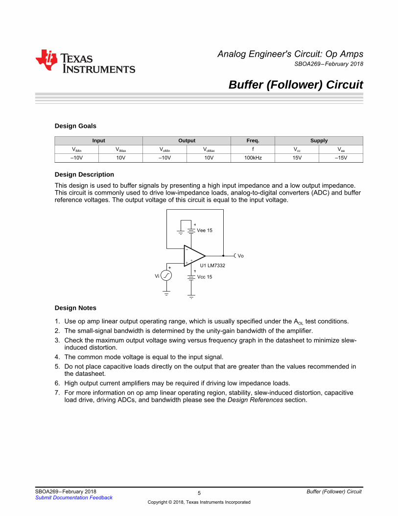
U1 LM7332
Vcc 15
Vee 15
+
Vi
Vo
SBOA269–February 2018Submit Documentation Feedback
Copyright © 2018, Texas Instruments Incorporated
Buffer (Follower) Circuit
Analog Engineer's Circuit: Op AmpsSBOA269–February 2018
Buffer (Follower) Circuit
Design Goals
Input Output Freq. SupplyViMin ViMax VoMin VoMax f Vcc Vee
–10V 10V –10V 10V 100kHz 15V –15V
Design DescriptionThis design is used to buffer signals by presenting a high input impedance and a low output impedance.This circuit is commonly used to drive low-impedance loads, analog-to-digital converters (ADC) and bufferreference voltages. The output voltage of this circuit is equal to the input voltage.
Design Notes
1. Use op amp linear output operating range, which is usually specified under the AOL test conditions.2. The small-signal bandwidth is determined by the unity-gain bandwidth of the amplifier.3. Check the maximum output voltage swing versus frequency graph in the datasheet to minimize slew-
induced distortion.4. The common mode voltage is equal to the input signal.5. Do not place capacitive loads directly on the output that are greater than the values recommended in
the datasheet.6. High output current amplifiers may be required if driving low impedance loads.7. For more information on op amp linear operating region, stability, slew-induced distortion, capacitive
load drive, driving ADCs, and bandwidth please see the Design References section.
5

www.ti.com
SBOA269–February 2018Submit Documentation Feedback
Copyright © 2018, Texas Instruments Incorporated
Buffer (Follower) Circuit
Design StepsThe tranfer function for this circuit is given below.
1. Verify that the amplifier can acheive the desired output swing using the supply voltages provided. Usethe output swing stated in the AOL test conditions. The output swing range of the amplifier must begreater than the output swing required for the design.
• The output swing of the LM7332 using ±15-V supplies is greater than the required output swing of thedesign. Therefore, this requirement is met.
• Review the Output Voltage versus Output Current curves in the product datasheet to verify the desiredoutput voltage can be acheived for the desired output current.
2. Verify the input common mode voltage of the amplifier will not be violated using the supply voltageprovided. The input common mode voltage range of the amplifier must be greater than the input signalvoltage range.
• The input common-mode range of the LM7332 using ±15-V supplies is greater than the required inputcommon-mode range of the design. Therefore, this requirement is met.
3. Calculate the minimum slew rate required to minimize slew-induced distortion.
• The slew rate of the LM7332 is 15.2V/µs. Therefore, this requirement is met.4. Verify the device will have sufficient bandwidth for the desired output signal frequency.
• The desired output signal frequency is less than the unity-gain bandwidth of the LM7332. Therefore,this requirement is met.
6

T
-3dB BW = 7.4MHz
Frequency (Hz)10 100 1k 10k 100k 1MEG 10MEG 100MEG
Gai
n (d
B)
-20
-15
-10
-5
0
-3dB BW = 7.4MHz
T
Input voltage (V)-10 -8 -6 -4 -2 0 2 4 6 8 10
Out
put V
olta
ge (V
)
-10
-8
-6
-4
-2
0
2
4
6
8
10
Input voltage (V)-10 -8 -6 -4 -2 0 2 4 6 8 10
Out
put V
olta
ge (V
)
-10
-8
-6
-4
-2
0
2
4
6
8
10
www.ti.com
SBOA269–February 2018Submit Documentation Feedback
Copyright © 2018, Texas Instruments Incorporated
Buffer (Follower) Circuit
Design SimulationsDC Simulation Results
AC Simulation Results
7

www.ti.com
SBOA269–February 2018Submit Documentation Feedback
Copyright © 2018, Texas Instruments Incorporated
Buffer (Follower) Circuit
Design ReferencesSee TIPD128, www.ti.com/tool/tipd128For more information on many op amp topics including common-mode range, output swing, bandwidth,slew rate, and how to drive an ADC please see TI Precision Labs.Design Featured Op Amp
LM7332Vss 2.5V to 32V
VinCM Rail-to-railVout Rail-to-railVos 1.6mVIq 2mAIb 1µA
UGBW 7.5MHz (±5-V supply)SR 15.2V/µs
#Channels 2www.ti.com/product/LM7332
Design Alternate Op Amp
OPA192Vss 4.5V to 36V
VinCM Rail-to-railVout Rail-to-railVos 5µVIq 1mAIb 5pA
UGBW 10MHzSR 20V/µs
#Channels 1, 2, 4www.ti.com/product/opa192
8

Vcc
Vee
Vee
Vcc
Vo
R2 20kR1 10k
+
Vi
-
++ U1 TLV170Vee 15
Vcc 15
Copyright © 2018, Texas Instruments Incorporated
SBOA270–February 2018Submit Documentation Feedback
Copyright © 2018, Texas Instruments Incorporated
Inverting Amplifier Circuit
Analog Engineer's Circuit: Op AmpsSBOA270–February 2018
Inverting Amplifier Circuit
Design Goals
Input Output Freq. SupplyViMin ViMax VoMin VoMax f Vcc Vee
–7V 7V –14V 14V 3kHz 15V –15V
Design DescriptionThis design inverts the input signal, Vi, and applies a signal gain of –2V/V. The input signal typicallycomes from a low-impedance source because the input impedance of this circuit is determined by theinput resistor, R1. The common-mode voltage of an inverting amplifier is equal to the voltage connected tothe non-inverting node, which is ground in this design.
Design Notes1. Use the op amp in a linear operating region. Linear output swing is usually specified under the AOL test
conditions. The common-mode voltage in this circuit does not vary with input voltage.2. The input impedance is determined by the input resistor. Make sure this value is large when compared
to the source's output impedance.3. Using high value resistors can degrade the phase margin of the circuit and introduce additional noise
in the circuit.4. Avoid placing capacitive loads directly on the output of the amplifier to minimize stability issues.5. Small-signal bandwidth is determined by the noise gain (or non-inverting gain) and op amp gain-
bandwidth product (GBP). Additional filtering can be accomplished by adding a capacitor in parallel toR2. Adding a capacitor in parallel with R2 will also improve stability of the circuit if high value resistorsare used.
6. Large signal performance may be limited by slew rate. Therefore, check the maximum output swingversus frequency plot in the data sheet to minimize slew-induced distortion.
7. For more information on op amp linear operating region, stability, slew-induced distortion, capacitiveload drive, driving ADCs, and bandwidth please see the Design References section.
9

www.ti.com
SBOA270–February 2018Submit Documentation Feedback
Copyright © 2018, Texas Instruments Incorporated
Inverting Amplifier Circuit
Design StepsThe transfer function of this circuit is given below.
1. Determine the starting value of R1. The relative size of R1 to the signal source's impedance affects thegain error. Assuming the signal source's impedance is low (for example, 100Ω), set R1=10kΩ for 1%gain error.
2. Calculate the gain required for the circuit. Since this is an inverting amplifier use ViMin and VoMax for thecalculation.
3. Calculate R2 for a desired signal gain of –2V/V.
4. Calculate the small signal circuit bandwidth to ensure it meets the 3kHz requirement. Be sure to usethe noise gain, or non-inverting gain, of the circuit.
5. Calculate the minimum slew rate required to minimize slew-induced distortion.
• SRTLV170=0.4V/µs, therefore it meets this requirement.6. To avoid stability issues ensure that the zero created by the gain setting resistors and input
capacitance of the device is greater than the bandwidth of the circuit.
• Ccm and Cdiff are the common-mode and differential input capacitances of the TLV170, respectively.• Since the zero frequency is greater than the bandwidth of the circuit, this requirement is met.
10

T
-3dB BW=519kHz
Frequency (Hz)1 10 100 1k 10k 100k 1M 10M
Gai
n (d
B)
-20.00
6.03
-3dB BW=519kHz
T
Input voltage (V)-7.0 -3.5 0.0 3.5 7.0
Vol
tage
(V)
-14.0
-7.0
0.0
7.0
14.0
www.ti.com
SBOA270–February 2018Submit Documentation Feedback
Copyright © 2018, Texas Instruments Incorporated
Inverting Amplifier Circuit
Design SimulationsDC Simulation Results
AC Simulation ResultsThe bandwidth of the circuit depends on the noise gain, which is 3V/V. The bandwidth is determined bylooking at the –3dB point, which is located at 3dB given a signal gain of 6dB. The simulation sufficientlycorrelates with the calculated value of 400kHz.
11

T
Time (s)0 250u 500u 750u 1m
Vol
tage
(V)
-13.99
0.00
13.99
www.ti.com
SBOA270–February 2018Submit Documentation Feedback
Copyright © 2018, Texas Instruments Incorporated
Inverting Amplifier Circuit
Transient Simulation ResultsThe output is double the magnitude of the input, and inverted.
12

www.ti.com
SBOA270–February 2018Submit Documentation Feedback
Copyright © 2018, Texas Instruments Incorporated
Inverting Amplifier Circuit
Design ReferencesFor more information on many op amp topics including common-mode range, output swing, bandwidth,and how to drive an ADC please visit TI Precision Labs.Design Featured Op Amp
TLV170Vss ±18V (36V)
VinCM (Vee-0.1V) to (Vcc-2V)Vout Rail-to-railVos 0.5mVIq 125µAIb 10pA
UGBW 1.2MHzSR 0.4V/µs
#Channels 1, 2, 4www.ti.com/product/tlv170
Design Alternate Op Amp
LMV358Vss 2.7 to 5.5V
VinCM (Vee–0.2V) to (Vcc–0.8V)Vout Rail-to-railVos 1.7mVIq 210µAIb 15nA
UGBW 1MHzSR 1V/µs
#Channels 1 (LMV321), 2 (LMV358), 4(LMV324)
www.ti.com/product/lmv358
13

VEE 15
VCC 15
-
++
U1 OPA171
+
Vi
R1 9.09k
Vo
R2 1.01k
SBOA271–January 2018Submit Documentation Feedback
Copyright © 2018, Texas Instruments Incorporated
Non-Inverting Amplifier Circuit
Analog Engineer's Circuit: Op AmpsSBOA271–January 2018
Non-Inverting Amplifier Circuit
Design Goals
Input Output SupplyViMin ViMax VoMin VoMax Vcc Vee–1V 1V –10V 10 15V –15V
Design DescriptionThis design amplifies the input signal, Vi, with a signal gain of 10V/V. The input signal may come from ahigh-impedance source (for example, MΩ) because the input impedance of this circuit is determined bythe extremely high input impedance of the op amp (for example, GΩ). The common-mode voltage of anon-inverting amplifier is equal to the input signal.
Design Notes
1. Use the op amp linear output operating range, which is usually specified under the AOL test conditions.The common-mode voltage is equal to the input signal.
2. The input impedance of this circuit is equal to the input impedance of the amplifier.3. Using high-value resistors can degrade the phase margin of the circuit and introduce additional noise
in the circuit.4. Avoid placing capacitive loads directly on the output of the amplifier to minimize stability issues.5. The small-signal bandwidth of a non-inverting amplifier depends on the gain of the circuit and the gain
bandwidth product (GBP) of the amplifier. Additional filtering can be accomplished by adding acapacitor in parallel to R1. Adding a capacitor in parallel with R1 will also improve stability of the circuitif high-value resistors are used.
6. Large signal performance may be limited by slew rate. Therefore, check the maximum output swingversus frequency plot in the data sheet to minimize slew-induced distortion.
7. For more information on op amp linear operating region, stability, slew-induced distortion, capacitiveload drive, driving ADCs, and bandwidth please see the Design References section.
14

www.ti.com
SBOA271–January 2018Submit Documentation Feedback
Copyright © 2018, Texas Instruments Incorporated
Non-Inverting Amplifier Circuit
Design StepsThe transfer function for this circuit is given below.
1. Calculate the gain.
2. Calculate values for R1 and R2.
3. Calculate the minimum slew rate required to minimize slew-induced distortion.
• The slew rate of the OPA171 is 1.5V/µs, therefore it meets this requirement.4. To maintain sufficient phase margin, ensure that the zero created by the gain setting resistors and
input capacitance of the device is greater than the bandwidth of the circuit.
• Ccm and Cdiff are the common-mode and differential input capacitances of the OPA171, respectively.• Since the zero frequency is greater than the bandwidth of the circuit, this requirement is met.
15

T
-3dB BW = 323.2kHz
Frequency (Hz)10 100 1k 10k 100k 1MEG 10MEG 100MEG
Gai
n (d
B)
-40
-30
-20
-10
0
10
20
-3dB BW = 323.2kHz
T
Input voltage (V)-1 -750m -500m -250m 0 250m 500m 750m 1
Out
put V
olta
ge (V
)
-10
-8
-6
-4
-2
0
2
4
6
8
10
www.ti.com
SBOA271–January 2018Submit Documentation Feedback
Copyright © 2018, Texas Instruments Incorporated
Non-Inverting Amplifier Circuit
Design SimulationsDC Simulation Results
AC Simulation Results
16

www.ti.com
SBOA271–January 2018Submit Documentation Feedback
Copyright © 2018, Texas Instruments Incorporated
Non-Inverting Amplifier Circuit
Design ReferencesFor more information on many op amp topics including common-mode range, output swing, andbandwidth please visit TI Precision Labs.Design Featured Op Amp
OPA171Vss 2.7V to 36V
VinCM (Vee–0.1V) to (Vcc–2V)Vout Rail-to-railVos 250µVIq 475µAIb 8pA
UGBW 3MHzSR 1.5V/µs
#Channels 1, 2, 4www.ti.com/product/opa171
Design Alternate Op Amp
OPA191Vss 4.5V to 36V
VinCM Rail-to-railVout Rail-to-railVos 5µVIq 140µAIb 5pA
UGBW 2.5MHzSR 7.5V/µs
#Channels 1, 2, 4www.ti.com/product/OPA191
17

Vcc
VccVee
Vee
R2 2.05k
R1 20.5k
R3 20k
Vcc 5
+
Vi1Vo
Vee 5
-
++
U1 TLV170
+
Vi2
++
Copyright © 2018, Texas Instruments Incorporated
SBOA272–February 2018Submit Documentation Feedback
Copyright © 2018, Texas Instruments Incorporated
Inverting Summer Circuit
Analog Engineer's Circuit: Op AmpsSBOA272–February 2018
Inverting Summer Circuit
Design Goals
Input 1 Input 2 Output Freq. SupplyVi1Min Vi1Max Vi2Min Vi2Max VoMin VoMax f Vcc Vee
–5V 5V –250mV 250mV –4.9V 4.9V 10kHz 5V –5V
Design DescriptionThis design sums (adds) and inverts two input signals, Vi1 and Vi2. The input signals typically come fromlow-impedance sources because the input impedance of this circuit is determined by the input resistors,R1 and R2. The common-mode voltage of an inverting amplifier is equal to the voltage connected to thenon-inverting node, which is ground in this design.
Design Notes1. Use the op amp in a linear operating region. Linear output swing is usually specified under the AOL test
conditions. The common-mode voltage in this circuit does not vary with input voltage.2. The input impedance is determined by the input resistors. Make sure these values are large when
compared to the output impedance of the source.3. Using high-value resistors can degrade the phase margin of the circuit and introduce additional noise
in the circuit.4. Avoid placing capacitive loads directly on the output of the amplifier to minimize stability issues.5. Small-signal bandwidth is determined by the noise gain (or non-inverting gain) and op amp gain-
bandwidth product (GBP). Additional filtering can be accomplished by adding a capacitor in parallel toR3. Adding a capacitor in parallel with R3 will also improve stability of the circuit if high-value resistorsare used.
6. Large signal performance may be limited by slew rate. Therefore, check the maximum output swingversus frequency plot in the data sheet to minimize slew-induced distortion.
7. For more information on op amp linear operating region, stability, slew-induced distortion, capacitiveload drive, driving ADCs, and bandwidth please see the Design References section.
18

www.ti.com
SBOA272–February 2018Submit Documentation Feedback
Copyright © 2018, Texas Instruments Incorporated
Inverting Summer Circuit
Design StepsThe transfer function for this circuit is given below.
1. Select a reasonable resistance value for R3.
2. Calculate gain required for Vi1. For this design, half of the output swing is devoted to each input.
3. Calculate the value of R1.
4. Calculate gain required for Vi2. For this design, half of the output swing is devoted to each input.
5. Calculate the value of R2.
6. Calculate the small signal circuit bandwidth to ensure it meets the 10-kHz requirement. Be sure to usethe noise gain (NG), or non-inverting gain, of the circuit. When calculating the noise gain note that R1and R2 are in parallel.
• This requirement is met because the closed-loop bandwidth is 102kHz and the design goal is 10kHz.7. Calculate the minmum slew rate to minimize slew-induced distortion.
• SROPA170=0.4V/µs, therefore it meets this requirement.8. To avoid stability issues ensure that the zero created by the gain setting resistors and input
capacitance of the device is greater than the bandwidth of the circuit.
• Ccm and Cdiff are the common-mode and differential input capacitances.• Since the zero frequency is greater than the bandwidth of the circuit, this requirement is met.
19

T
Vo=2.44V
Vo=-2.44V
Input voltage (Vi2)-250.00m 0.00 250.00m
Vol
tage
(V)
-2.5
0.0
2.5
Vo=-2.44V
Vo=2.44V
Vi1 held constant (0V)Vi2 swept from -250mV to 250mV
T
Vo=2.44V
Vo=-2.44V
Input voltage (Vi1)-2.5 0.0 2.5
Vol
tage
(V)
-2.5
0.0
2.5
Vo=-2.44V
Vo=2.44V
Vi2 held constant (0V)Vi1 swept from -2.5V to 2.5V
www.ti.com
SBOA272–February 2018Submit Documentation Feedback
Copyright © 2018, Texas Instruments Incorporated
Inverting Summer Circuit
Design SimulationsDC Simulation ResultsThis simulation sweeps Vi1 from –2.5V to 2.5V while Vi2 is held constant at 0V. The output is inverted andranges from –2.44V to 2.44V.
This simulation sweeps Vi2 from –250mV to 250mV while Vi1 is held constant at 0V. The output is invertedand ranges from –2.44V to 2.44V.
20
T
Time (s)0.00 1.50m 3.00m
Vi1
-2.50
2.50
Vi2
-250.00m
250.00m
Vo
-4.84
4.85
T
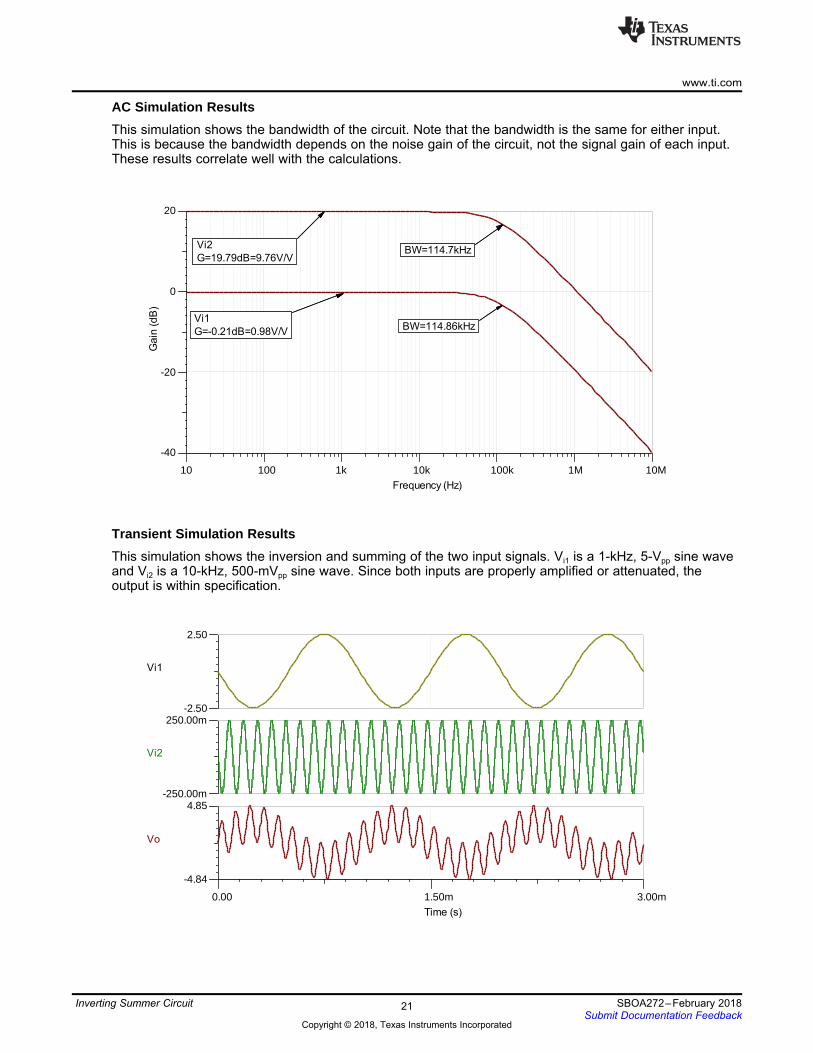
Vi1G=-0.21dB=0.98V/V BW=114.86kHz
Vi2G=19.79dB=9.76V/V
BW=114.7kHz
Frequency (Hz)10 100 1k 10k 100k 1M 10M
Gai
n (d
B)
-40
-20
0
20
BW=114.86kHz
BW=114.7kHzVi2G=19.79dB=9.76V/V
Vi1G=-0.21dB=0.98V/V
www.ti.com
SBOA272–February 2018Submit Documentation Feedback
Copyright © 2018, Texas Instruments Incorporated
Inverting Summer Circuit
AC Simulation ResultsThis simulation shows the bandwidth of the circuit. Note that the bandwidth is the same for either input.This is because the bandwidth depends on the noise gain of the circuit, not the signal gain of each input.These results correlate well with the calculations.
Transient Simulation ResultsThis simulation shows the inversion and summing of the two input signals. Vi1 is a 1-kHz, 5-Vpp sine waveand Vi2 is a 10-kHz, 500-mVpp sine wave. Since both inputs are properly amplified or attenuated, theoutput is within specification.
21

www.ti.com
SBOA272–February 2018Submit Documentation Feedback
Copyright © 2018, Texas Instruments Incorporated
Inverting Summer Circuit
Design ReferencesFor more information on many op amp topics including common-mode range, output swing, bandwidth,and how to drive an ADC please visit TI Precision Labs.Design Featured Op Amp
OPA170Vss 2.7V to 36V
VinCM (Vee-0.1V) to (Vcc-2V)Vout Rail-to-railVos 0.25mVIq 110µAIb 8pA
UGBW 1.2MHzSR 0.4V/µs
#Channels 1, 2, 4www.ti.com/product/opa170
Design Alternate Op Amp
LMC7101Vss 2.7V to 15.5V
VinCM Rail-to-railVout Rail-to-railVos 110µVIq 0.8mAIb 1pA
UGBW 1.1MHzSR 1.1V/µs
#Channels 1www.ti.com/product/lmc7101
22

Vcc
Vee
Vcc
Vref
Vee
Vref
Vo
R3 20kR1 10k
-
++
U1 TLV6001
R2 10k
Vcc 2.75
R4 20k
Vee 2.75
Vref 0
Vi1
Vi2+
+
+
+
+
Copyright © 2018, Texas Instruments Incorporated
SBOA274–February 2018Submit Documentation Feedback
Copyright © 2018, Texas Instruments Incorporated
Difference Amplifier (Subtractor) Circuit
Analog Engineer's Circuit: Op AmpsSBOA274–February 2018
Difference Amplifier (Subtractor) Circuit
Design Goals
Input (Vi2-Vi1) Output CMRR (min) SupplyVidiffMin VidiffMax VoMin VoMax dB Vcc Vee Vref
–1.25V 1.25V –2.5V 2.5V 50 2.75V –2.75V 0V
Design DescriptionThis design inputs two signals, Vi1 and Vi2, and outputs their difference (subtracts). The input signalstypically come from low-impedance sources because the input impedance of this circuit is determined bythe resistive network. Difference amplifiers are typically used to amplify differential input signals and rejectcommon-mode voltages. A common-mode voltage is the voltage common to both inputs. Theeffectiveness of the ability of a difference amplifier to reject a common-mode signal is known as common-mode rejection ratio (CMRR). The CMRR of a difference amplifier is dominated by the tolerance of theresistors.
Design Notes1. Use the op amp in a linear operating region. Ensure that the inputs of the op amp do not exceed the
common-mode range of the device. Linear output swing is usually specified under the AOL testconditions.
2. The input impedance is determined by the input resistive network. Make sure these values are largewhen compared to the output impedance of the sources.
3. Using high-value resistors can degrade the phase margin of the circuit and introduce additional noisein the circuit.
4. Avoid placing capacitive loads directly on the output of the amplifier to minimize stability issues.5. Small-signal bandwidth is determined by the noise gain (or non-inverting gain) and op amp gain-
bandwidth product (GBP). Additional filtering can be accomplished by adding a capacitors in parallel toR3 and R4. Adding capacitors in parallel with R3 and R4 will also improve stability of the circuit if high-value resistors are used.
6. Large signal performance may be limited by slew rate. Therefore, check the maximum output swingversus frequency plot in the data sheet to minimize slew-induced distortion.
7. For more information on op amp linear operating region, stability, slew-induced distortion, capacitiveload drive, driving ADCs, and bandwidth please see the Design References section.
23

www.ti.com
SBOA274–February 2018Submit Documentation Feedback
Copyright © 2018, Texas Instruments Incorporated
Difference Amplifier (Subtractor) Circuit
Design StepsThe complete transfer function for this circuit is shown below.
If R1 = R2 and R3 = R4 the transfer function for this circuit simplifies to the following equation.
• Where the gain, G, is R3/R1.
1. Determine the starting value of R1 and R2. The relative size of R1 and R2 to the signal impedance of thesource affects the gain error.
2. Calculate the gain required for the circuit.
3. Calculate the values for R3 and R4.
4. Calculate resistor tolerance to meet the minimum common-mode rejection ratio (CMRR). For minimum(worst-case) CMRR, α = 4. For a more probable, or typical value of CMRR, α = 0.33.
5. For quick reference, the following table compares resistor tolerance to minimum and typical CMRRvalues assuming G = 1 or G = 2. As shown above, as gain increases so does CMRR.
Tolerance G=1 Minimum (dB) G=1 Typical (dB) G=2 Minimum (dB) G=2 Typical (dB)0.01%=0.0001 74 95.6 77.5 99.2
0.1%=0.001 54 75.6 57.5 79.20.5%=0.005 40 61.6 43.5 65.2
1%=0.01 34 55.6 37.5 59.25%=0.05 20 41.6 23.5 45.2
24

T
Worst Case CMRR=-51.11dBData sheets typically depict CMRR asa positive number.
Frequency (Hz)10 20
Gai
n (d
B)
-80
-60
-40
Worst Case CMRR=-51.11dBData sheets typically depict CMRR asa positive number.
This value is referred to the output.To refer to input, subtract the gain in dB,which is 6dB (2V/V). Actual CMRRreferred to the input is therefore -57.11dB
T
Input voltage (Vdiff)-1.25 -750.00m -250.00m 250.00m 750.00m 1.25
Out
put
-2.5
-1.5
-500.0m
500.0m
1.5
2.5
Vdiff=Vi2-Vi1
www.ti.com
SBOA274–February 2018Submit Documentation Feedback
Copyright © 2018, Texas Instruments Incorporated
Difference Amplifier (Subtractor) Circuit
Design SimulationsDC Simulation Results
CMRR Simulation Results
25

www.ti.com
SBOA274–February 2018Submit Documentation Feedback
Copyright © 2018, Texas Instruments Incorporated
Difference Amplifier (Subtractor) Circuit
Design ReferencesFor more information on many op amp topics including common-mode range, output swing, bandwidth,and how to drive an ADC please visit TI Precision Labs. For more information on difference amplifierCMRR, please read Overlooking the obvious: the input impedance of a difference amplifier .Design Featured Op Amp
TLV6001Vss 1.8V to 5.5V
VinCM Rail-to-railVout Rail-to-railVos 750µVIq 75µAIb 1pA
UGBW 1MHzSR 0.5V/µs
#Channels 1, 2, 4www.ti.com/product/tlv6001
Design Alternate Op Amp
OPA320Vss 1.8V to 5.5V
VinCM Rail-to-railVout Rail-to-railVos 40µVIq 1.5mAIb 0.2pA
UGBW 20MHzSR 10V/µs
#Channels 1, 2www.ti.com/product/opa320
26

Vcc
Vee
Vee
Vcc
R1 100k C1 1.59n
+
Vin
Vout
R2 100M
Vos -740u
-
++
U1 TLV9002
Vcc 2.5
Vee 2.5
Copyright © 2018, Texas Instruments Incorporated
SBOA275–February 2018Submit Documentation Feedback
Copyright © 2018, Texas Instruments Incorporated
Integrator Circuit
Analog Engineer's Circuit: Op AmpsSBOA275–February 2018
Integrator Circuit
Design Goals
Input Output SupplyfMin f0dB fMax VoMin VoMax Vcc Vee
100Hz 1kHz 100kHz –2.45V 2.45V 2.5V –2.5V
Design DescriptionThe integrator circuit outputs the integral of the input signal over a frequency range based on the circuittime constant and the bandwidth of the amplifier. The input signal is applied to the inverting input so theoutput is inverted relative to the polarity of the input signal. The ideal integrator circuit will saturate to thesupply rails depending on the polarity of the input offset voltage and requires the addition of a feedbackresistor, R2, to provide a stable DC operating point. The feedback resistor limits the lower frequency rangeover which the integration function is performed. This circuit is most commonly used as part of a largerfeedback/servo loop which provides the DC feedback path, thus removing the requirement for a feedbackresistor.
Design Notes1. Use as large of a value as practical for the feedback resistor.2. Select a CMOS op amp to minimize the errors from the input bias current.3. The gain bandwidth product (GBP) of the amplifier will set the upper frequency range of the integrator
function. The effectiveness of the integration function is usually reduced starting about one decadeaway from the amplifier bandwidth.
4. An adjustable reference needs to be connected to the non-inverting input of the op amp to cancel theinput offset voltage or the large DC noise gain will cause the circuit to saturate. Op amps with very lowoffset voltage may not require this.
27

T
-38.6dB @ 100kHz
40dB @ 10Hz
0dB @ 1kHz
Frequency (Hz)1 10 100 1k 10k 100k 1M
Gai
n (d
B)
-60
-40
-20
0
20
40
60
0dB @ 1kHz
40dB @ 10Hz
-38.6dB @ 100kHz
www.ti.com
SBOA275–February 2018Submit Documentation Feedback
Copyright © 2018, Texas Instruments Incorporated
Integrator Circuit
Design StepsThe ideal circuit transfer function is given below.
1. Set R1 to a standard value.
2. Calculate C1 to set the unity-gain integration frequency.
3. Calculate R2 to set the lower cutoff frequency a decade less than the minimum operating frequency.
4. Select an amplifier with a gain bandwidth at least 10 times the desired maximum operating frequency.
Design SimulationsAC Simulation Results
28
Time (s)100m 102.5m 105m
Vin
-100m
100m
Vout
-76.77m
77.53m
Time (s)100m 102.5m 105m
Vin
-100m
0
100m
Vout
-100m
0
100m
www.ti.com
SBOA275–February 2018Submit Documentation Feedback
Copyright © 2018, Texas Instruments Incorporated
Integrator Circuit
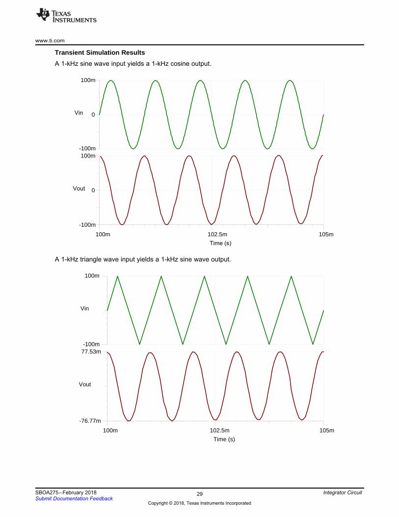
Transient Simulation ResultsA 1-kHz sine wave input yields a 1-kHz cosine output.
A 1-kHz triangle wave input yields a 1-kHz sine wave output.
29

T
Time (s)100m 102.5m 105m
Vin
-100m
100m
Vout
-136.45m
186.58m
www.ti.com
SBOA275–February 2018Submit Documentation Feedback
Copyright © 2018, Texas Instruments Incorporated
Integrator Circuit
A 1-kHz square wave input yields a 1-kHz triangle wave output.
Design ReferencesSee TIPD191, www.ti.com/tool/tipd191.
30

www.ti.com
SBOA275–February 2018Submit Documentation Feedback
Copyright © 2018, Texas Instruments Incorporated
Integrator Circuit
Design Featured Op Amp
TLV9002Vcc 1.8V to 5.5V
VinCM Rail-to-railVout Rail-to-railVos 0.4mVIq 0.06mAIb 5pA
UGBW 1MHzSR 2V/µs
#Channels 1, 2, 4www.ti.com/product/tlv9002
Design Alternate Op Amp
OPA376Vcc 2.2V to 5.5V
VinCM (Vee-0.1V) to (Vcc-1.3V)Vout Rail-to-railVos 0.005mVIq 0.76mAIb 0.2pA
UGBW 5.5MHzSR 2V/µs
#Channels 1, 2, 4www.ti.com/product/opa376
31
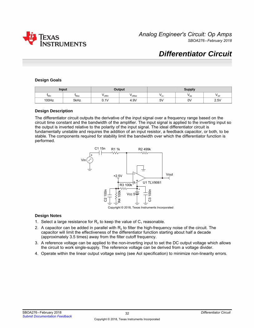
+2.5V Vout
+
Vin
Vcc 5
R2 499kR1 1kC
3 10
0n
-
++ U1 TLV9061
C1 15n
R3 100k
R4
100k
C2
100n
Copyright © 2018, Texas Instruments Incorporated
SBOA276–February 2018Submit Documentation Feedback
Copyright © 2018, Texas Instruments Incorporated
Differentiator Circuit
Analog Engineer's Circuit: Op AmpsSBOA276–February 2018
Differentiator Circuit
Design Goals
Input Output SupplyfMin fMax VoMin VoMax Vcc Vee Vref
100Hz 5kHz 0.1V 4.9V 5V 0V 2.5V
Design DescriptionThe differentiator circuit outputs the derivative of the input signal over a frequency range based on thecircuit time constant and the bandwidth of the amplifier. The input signal is applied to the inverting input sothe output is inverted relative to the polarity of the input signal. The ideal differentiator circuit isfundamentally unstable and requires the addition of an input resistor, a feedback capacitor, or both, to bestable. The components required for stability limit the bandwidth over which the differentiator function isperformed.
Design Notes1. Select a large resistance for R2 to keep the value of C1 reasonable.2. A capacitor can be added in parallel with R2 to filter the high-frequency noise of the circuit. The
capacitor will limit the effectiveness of the differentiator function starting about half a decade(approximately 3.5 times) away from the filter cutoff frequency.
3. A reference voltage can be applied to the non-inverting input to set the DC output voltage which allowsthe circuit to work single-supply. The reference voltage can be derived from a voltage divider.
4. Operate within the linear output voltage swing (see Aol specification) to minimize non-linearity errors.
32

www.ti.com
SBOA276–February 2018Submit Documentation Feedback
Copyright © 2018, Texas Instruments Incorporated
Differentiator Circuit
Design StepsThe ideal circuit transfer function is given below.
1. Set R2 to a large standard value.
2. Set the minimum differentiation frequency at least half a decade below the minimum operatingfrequency.
3. Set the upper cutoff frequency at least half a decade above the maximum operating frequency.
4. Calculate the necessary op amp gain bandwidth product (GBP) for the circuit to be stable.
• The bandwidth of the TLV9061 is 10MHz, therefore this requirement is met.5. If a feedback capacitor, CF , is added in parallel with R2, the equation to calculate the cutoff frequency
follows.
6. Calculate the resistor divider values for a 2.5-V reference voltage.
33

Time (s)1.00m 2.25m 3.50m
Vin
-20m
20m
Vout
128m
4.87
T
Gai
n (d
B)
-40
-20
0
20
40
60
Frequency (Hz)10 100 1k 10k 100k 1M 10M
Phas
e [d
eg]
-270
-225
-180
-135
-90
41.4dB @ 2.5kHz
13.4dB @ 100Hz
www.ti.com
SBOA276–February 2018Submit Documentation Feedback
Copyright © 2018, Texas Instruments Incorporated
Differentiator Circuit
Design SimulationsAC Simulation Results
Transient Simulation ResultsA 2.5-kHz sine wave input yields a 2.5-kHz cosine output.
34

Time (s)1m 25.5m 50m
Vin
-20m
20m
Vout
2.43
2.57
T
Time (s)100.00u 1.30m 2.50m
Vin
-1 m
1 m
Vout
1.84
3.16
www.ti.com
SBOA276–February 2018Submit Documentation Feedback
Copyright © 2018, Texas Instruments Incorporated
Differentiator Circuit
A 2.5-kHz square wave input produces an impulse output.
A 100-Hz triangle wave input yields a square wave output.
35

www.ti.com
SBOA276–February 2018Submit Documentation Feedback
Copyright © 2018, Texas Instruments Incorporated
Differentiator Circuit
Design Featured Op Amp
TLV9061Vcc 1.8V to 5.5V
VinCM Rail-to-railVout Rail-to-railVos 0.3mVIq 0.538mAIb 0.5pA
UGBW 10MHzSR 6.5V/µs
#Channels 1, 2, 4www.ti.com/product/tlv9061
Design Alternate Op Amp
OPA374Vcc 2.3V to 5V
VinCM Rail-to-railVout Rail-to-railVos 1mVIq 0.585mAIb 0.5pA
UGBW 6.5MHzSR 0.4V/µs
#Channels 1, 2, 4www.ti.com/product/opa374
36

V+
V-
V-
V+
Vout
R1 100k
C2
100n
Vcc 15
C3
100n
Vee 15Ii
C1 150p
-
+ +U1 OPA170
Copyright © 2018, Texas Instruments Incorporated
SBOA268–February 2018Submit Documentation Feedback
Copyright © 2018, Texas Instruments Incorporated
Transimpedance Amplifier Circuit
Analog Engineer's Circuit: Op AmpsSBOA268–February 2018
Transimpedance Amplifier Circuit
Design Goals
Input Output BW SupplyIiMin IiMax VoMin VoMax fp Vcc Vee
0A 50µA 0V 5V 10kHz 15V –15V
Design DescriptionThe transimpedance op amp circuit configuration converts an input current source into an output voltage.The current to voltage gain is based on the feedback resistance. The circuit is able to maintain a constantvoltage bias across the input source as the input current changes which benefits many sensors.
Design Notes1. Use a JFET or CMOS input op amp with low bias current to reduce DC errors.2. A bias voltage can be added to the non-inverting input to set the output voltage for 0-A input currents.3. Operate within the linear output voltage swing (see Aol specification) to minimize non-linearity errors.
37

www.ti.com
Transimpedance Amplifier Circuit SBOA268ïFebruary2018Submit Documentation Feedback
Copyright © 2018, Texas Instruments Incorporated
Design Steps1. Select the gain resistor.
2. Select the feedback capacitor to meet the circuit bandwidth.
3. Calculate the necessary op amp gain bandwidth (GBW) for the circuit to be stable.
• Cs: Input source capacitance• Cd: Differential input capacitance of the amplifier• Ccm: Common-mode input capacitance of the inverting input

www.ti.com
SBOA268–February 2018Submit Documentation Feedback
Copyright © 2018, Texas Instruments Incorporated
Transimpedance Amplifier Circuit
Design SimulationsDC Simulation Results
AC Simulation Results
39

www.ti.com
SBOA268–February 2018Submit Documentation Feedback
Copyright © 2018, Texas Instruments Incorporated
Transimpedance Amplifier Circuit
Design ReferencesSee TIPD176, www.ti.com/tool/tipd176.Design Featured Op Amp
OPA170Vcc 2.7V to 36V
VinCM (Vee–0.1V) to (Vcc –2V)Vout Rail–to–railVos 0.25mVIq 0.11mAIb 8pA
UGBW 1.2MHzSR 0.4V/µs
#Channels 1, 2, 4www.ti.com/product/opa170
Design Alternate Op Amp
OPA145Vcc 4.5V to 36V
VinCM (Vee–0.1V) to (Vcc –3.5V)Vout Rail–to–railVos 40µVIq 0.445mAIb 2pA
UGBW 5.5MHzSR 20V/µs
#Channels 1, 2, 4www.ti.com/product/opa145
40

Vee
Vcc
VeeVcc
Vee -230mVcc 5
R4 10k
Ii R1 100m
-
++
U1 OPA320Vi
Vo
R3 360kR2 7.5k
Copyright © 2018, Texas Instruments Incorporated
SBOA215–February 2018
© 2018, Texas Instruments Incorporated
Single-Supply, Low-Side, Unidirectional Current-Sensing Solution with Output Swing to GND Circuit
Analog Engineer's Circuit: Op AmpsSBOA215–February 2018
Single-Supply, Low-Side, Unidirectional Current-SensingSolution with Output Swing to GND Circuit
Design Goals
Input Output SupplyIiMin IiMax VoMin VoMax Vcc Vee Vref
0A 1A 0V 4.9V 5V 0V 0V
Design DescriptionThis single-supply, low-side, current sensing solution accurately detects load current between 0A to 1Aand converts it to a voltage between 0V to 4.9V. The input current range and output voltage range can bescaled as necessary and larger supplies can be used to accommodate larger swings. A negative chargepump (such as the LM7705) is used as the negative supply in this design to maintain linearity for outputsignals near 0V.
Design Notes1. Use precision resistors to minimize gain error.2. For light load accuracy, the negative supply should extend slightly below ground.3. A capacitor placed in parallel with the feedback resistor will limit bandwidth and help reduce noise.
41

www.ti.com
SBOA215–February 2018
Design Steps1. Determine the transfer function.
2. Define the full-scale shunt voltage and shunt resistance.
3. Select gain resistors to set the output range.
4. Select a standard value for R2 and R3.
42© 2018, Texas Instruments Incorporated
Single-Supply, Low-Side, Unidirectional Current-Sensing Solution with Output Swing to GND Circuit

www.ti.com
SBOA215–February 2018
© 2018, Texas Instruments Incorporated
Design SimulationsDC Simulation Results
AC Simulation Results
43 Single-Supply, Low-Side, Unidirectional Current-Sensing Solution with Output Swing to GND Circuit

www.ti.com
SBOA215–February 2018
Design ReferencesSee TIPD129, www.ti.com/tool/tipd129.Design Featured Op Amp
OPA320Vcc 1.8V to 5.5V
VinCM Rail-to-railVout Rail-to-railVos 40µVIq 1.5mA/ChIb 0.2pA
UGBW 10MHzSR 10V/µs
#Channels 1, 2www.ti.com/product/opa320
Design Alternate Op Amp
TLV9002Vcc 1.8V to 5.5V
VinCM Rail-to-railVout Rail-to-railVos 400µVIq 60µAIb 5pA
UGBW 1MHzSR 2V/µs
#Channels 1, 2, 4www.ti.com/product/tlv9002
44© 2018, Texas Instruments Incorporated
Single-Supply, Low-Side, Unidirectional Current-Sensing Solution with Output Swing to GND Circuit

VccVcc
Vcc
Vcc
Rshunt 100m
R1 1.3k
R3 1.3k
R2 20k
R4 20k
Vo
IiVbus 10
R6 10k
R5 10kVcc 3.3
+
-
V+U1 OPA313
+
-
V+U2 OPA313
V
+
Vshunt
Vref
Copyright © 2018, Texas Instruments Incorporated
SBOA223–February 2018Submit Documentation Feedback
Copyright © 2018, Texas Instruments Incorporated
Low-Side, Bidirectional Current Sensing Circuit
Analog Engineer's Circuit: Op AmpsSBOA223–February 2018
Low-Side, Bidirectional Current Sensing Circuit
Design Goals
Input Output SupplyIiMin IiMax VoMin VoMax Vcc Vee Vref
–1A 1A 110mV 3.19V 3.3V 0V 1.65V
Design DescriptionThis single-supply low-side, bidirectional current sensing solution can accurately detect load currents from–1A to 1A. The linear range of the output is from 110mV to 3.19V. Low-side current sensing keeps thecommon-mode voltage near ground, and is thus most useful in applications with large bus voltages.
Design Notes1. To minimize errors, set R3 = R1 and R4 = R2.2. Use precision resistors for higher accuracy.3. Set output range based on linear output swing (see Aol specification).4. Low-side sensing should not be used in applications where the system load cannot withstand small
ground disturbances or in applications that need to detect load shorts.
45

www.ti.com
SBOA223–February 2018Submit Documentation Feedback
Copyright © 2018, Texas Instruments Incorporated
Low-Side, Bidirectional Current Sensing Circuit
Design Steps1. Determine the transfer equation given R4 = R2 and R1 = R3.
2. Determine the maximum shunt resistance.
3. Set reference voltage.a. Since the input current range is symmetric, the reference should be set to mid supply. Therefore,
make R5 and R6 equal.
4. Set the difference amplifier gain based on the op amp output swing. The op amp output can swingfrom 100mV to 3.2V, given a 3.3-V supply.
46

T
Gai
n (d
B)
-20
-10
0
10
20
Frequency (Hz)10 100 1k 10k 100k 1M 10M
Phas
e [d
eg]
-270
-225
-180
-135
-90
-45
0
-3dB frequency = 77kHz
Ii = 1AVo = 3.2V
Ii = 0A
Ii = -1AVo = 121mV
Input current (A)-1 -500m 0 500m 1
Out
put V
olta
ge (V
)
0
1
2
3
4
Ii = -1AVo = 121mV
Ii = 0AVo = 1.66V
Ii = 1AVo = 3.2V
www.ti.com
SBOA223–February 2018Submit Documentation Feedback
Copyright © 2018, Texas Instruments Incorporated
Low-Side, Bidirectional Current Sensing Circuit
Design SimulationsDC Simulation Results
Closed Loop AC Simulation Results
47

Time (s)0.0 500.0u 1.0m 1.5m 2.0m
Ii (A)
-1
1
Vo (V)
0.0
3.3
Vref (V)
0.00
1.65
3.30
Vshunt (V)
-100m
100m
www.ti.com
SBOA223–February 2018Submit Documentation Feedback
Copyright © 2018, Texas Instruments Incorporated
Low-Side, Bidirectional Current Sensing Circuit
Transient Simulation Results
48

www.ti.com
SBOA223–February 2018Submit Documentation Feedback
Copyright © 2018, Texas Instruments Incorporated
Low-Side, Bidirectional Current Sensing Circuit
Design ReferencesSee TIPD175, www.ti.com/tipd175.Design Featured Op Amp
OPA313Vcc 1.8V to 5.5V
VinCM Rail-to-railVout Rail-to-railVos 500µVIq 50µA/ChIb 0.2pA
UGBW 1MHzSR 0.5V/µs
#Channels 1, 2, 4www.ti.com/product/opa313
Design Alternate Op Amp
TLV9062Vcc 1.8V to 5.5V
VinCM Rail-to-railVout Rail-to-railVos 300µVIq 538µA/ChIb 0.5pA
UGBW 10MHzSR 6.5V/µs
#Channels 1, 2, 4www.ti.com/product/tlv9062
Design Alternate Op Amp
OPA376Vcc 2.2V to 5.5V
VinCM Rail-to-railVout Rail-to-railVos 5µVIq 760µA/ChIb 0.2pA
UGBW 5.5MHzSR 2V/µs
#Channels 1, 2, 4www.ti.com/product/opa376
49

R4 50kR5 100
C4 1u
Vcc 5
R2 10M
++
-R1
R1
R2
U1 INA326
R3 511kC1 100n
C2 10p
C3 194p
R6 100k
VoVbus 5
Ii 10u
R1 25
SW1
Vi
Copyright © 2018, Texas Instruments Incorporated
SBOA210–January 2018Submit Documentation Feedback
Copyright © 2018, Texas Instruments Incorporated
3-Decade, Load-Current Sensing Circuit
Analog Engineer's Circuit: Op AmpsSBOA210–January 2018
3-Decade, Load-Current Sensing Circuit
Design Goals
Input Output SupplyIiMin IiMax VoMin VoMax Vcc Vee Vref
10μA 10mA 100mV 4.9V 5.0V 0V 0V
Design DescriptionThis single-supply, low-side, current-sensing solution accurately detects load current between 10μA and10mA. A unique yet simple gain switching network was implemented to accurately measure the three-decade load current range.
Design Notes1. Use a maximum shunt resistance to minimize relative error at minimum load current.2. Select 0.1% tolerance resistors for R1, R2, R3, and R4 in order to achieve approximately 0.1% FSR gain
error.3. Use a switch with low on-resistance (Ron) to minimize interaction with feedback resistances, preserving
gain accuracy.4. Minimize capacitance on INA326 gain setting pins.5. Scale the linear output swing based on the gain error specification.
50

www.ti.com
SBOA210–January 2018Submit Documentation Feedback
Copyright © 2018, Texas Instruments Incorporated
3-Decade, Load-Current Sensing Circuit
Design Steps1. Define full-scale shunt resistance.
2. Select gain resistors to set output range.
3. Select a capacitor for the output filter.
4. Select a capacitor for gain and filtering network.
51

T
Frequency (Hz)1 10 100 1k 10k 100k 1M
Gai
n (d
B)
-100
-80
-60
-40
-20
0
20
40
60
BW=1.02kHz
BW=852.6Hz
G=25.71dB
G=51.94dB
T
G=19.6 VV
G=400 VV
Input current (A)0.0 2.5m 5.0m 7.5m 10.0m
Volta
ge (V
)
0.0
1.0
2.0
3.0
4.0
5.0
www.ti.com
SBOA210–January 2018Submit Documentation Feedback
Copyright © 2018, Texas Instruments Incorporated
3-Decade, Load-Current Sensing Circuit
Design SimulationsDC Simulation Results
AC Simulation Results
52

www.ti.com
SBOA210–January 2018Submit Documentation Feedback
Copyright © 2018, Texas Instruments Incorporated
3-Decade, Load-Current Sensing Circuit
Design ReferencesSee TIPD104, www.ti.com/tool/tipd104.Design Featured Op Amp
INA326Vss 1.8V to 5.5V
VinCM Rail-to-railVout Rail-to-railVos 0.1mVIq 3.4mAIb 2nA
UGBW 1kHzSR Filter limited
#Channels 1www.ti.com/product/ina326
53

Vcc
Vref
VrefVcc
Vcc
Vcc
Vref
R5 8.45kR6 10k
C3 100p
R7 5.9k
-
++
U4 TLV3501
+
-
+U3 OPA365
R3 10k
R4 10k
C1 100p
R1
10k
C2
100n
-
++
U2 TLV3501+
ViVo
R2
10k
Vtri
Vsin
+
-
+U1 OPA365
V1
Error Amplifier Comparator Triangle Wave Generator
Copyright © 2018, Texas Instruments Incorporated
SBOA212–January 2018Submit Documentation Feedback
Copyright © 2018, Texas Instruments Incorporated
PWM Generator Circuit
Analog Engineer's Circuit: Op AmpsSBOA212–January 2018
PWM Generator Circuit
Design Goals
Input Output SupplyViMin ViMax VoMin VoMax Vcc Vee Vref
–2.0V 2.0V 0V 5V 5V 0V 2.5V
Design DescriptionThis circuit utilizes a triangle wave generator and comparator to generate a 500 kHz pulse-width-modulated (PWM) waveform with a duty cycle that is inversely proportional to the input voltage. An opamp and comparator (U3 and U4) generate a triangle waveform which is applied to the inverting input of asecond comparator (U2). The input voltage is applied to the non-inverting input of U2. By comparing theinput waveform to the triangle wave, a PWM waveform is produced. U2 is placed in the feedback loop ofan error amplifier (U1) to improve the accuracy and linearity of the output waveform.
Design Notes1. Use a comparator with push-pull output and minimal propagation delay.2. Use an op amp with sufficient slew rate, GBW, and voltage output swing.3. Place the pole created by C1 below the switching frequency and well above the audio range.4. Vref must be low impedance (for example, output of an op amp).
54

www.ti.com
SBOA212–January 2018Submit Documentation Feedback
Copyright © 2018, Texas Instruments Incorporated
PWM Generator Circuit
Design Steps
1. Set the error amplifier inverting signal gain.
2. Determine R1 and R2 to divide Vref to cancel the non-inverting gain.
3. The amplitude of Vtri must be chosen such that it is greater than the maximum amplitude of Vi (2.0V) toavoid 0% or 100% duty cycle in the PWM output signal. Select Vtri to be 2.1V. The amplitude of V1 =2.5V.
4. Set the oscillation frequency to 500kHz.
5. Choose C1 to limit amplifier bandwidth to below switching frequency.
6. Select C2 to filter noise from Vref.
55

T
Time (s)50.0u 60.0u 70.0u 80.0u 90.0u 100.0u
VIN
-2.0
-1.0
0.0
1.0
2.0
Vout
0.0
2.5
5.0
T
Input voltage (V)-2.0 -1.0 0.0 1.0 2.0
Out
put
0.0
500.0m
1.0
1.5
2.0
2.5
3.0
3.5
4.0
4.5
5.0
www.ti.com
SBOA212–January 2018Submit Documentation Feedback
Copyright © 2018, Texas Instruments Incorporated
PWM Generator Circuit
Design SimulationsDC Simulation Results
Transient Simulation Results
56

www.ti.com
SBOA212–January 2018Submit Documentation Feedback
Copyright © 2018, Texas Instruments Incorporated
PWM Generator Circuit
Design ReferencesSee TIPD108, www.ti.com/tool/tipd108Design Featured Op Amp
OPA2365Vss 2.2V to 5.5V
VinCM Rail-to-railVout Rail-to-railVos 100µVIq 4.6mAIb 2pA
UGBW 50MHzSR 25V/µs
#Channels 2www.ti.com/product/opa2365
Design Comparator
TLV3502Vss 2.2V to 5.5V
VinCM Rail-to-railVout Rail-to-railVos 1mVIq 3.2mAIb 2pA
UGBW -SR -
#Channels 2www.ti.com/product/tlv3502
Design Alternate Op Amp
OPA2353Vss 2.7V to 5.5V
VinCM Rail-to-railVout Rail-to-railVos 3mVIq 5.2mAIb 0.5pA
UGBW 44MHzSR 22V/µs
#Channels 2www.ti.com/product/opa2353
57

Vcc +5V
+
Vi
Vinp
C1 10u
V
R1 1k R4 10k
+
-
+SD
U1 LMV981
Vref +5V
C2 10u R3 4.99k
R2 4.99k
Copyright © 2018, Texas Instruments Incorpor
SBOA222–February 2018Submit Documentation Feedback
Copyright © 2018, Texas Instruments Incorporated
AC Coupled (HPF) Inverting Amplifier Circuit
Analog Engineer's Circuit: Op AmpsSBOA222–February 2018
AC Coupled (HPF) Inverting Amplifier Circuit
Design Goals
Input Output SupplyViMin ViMax VoMin VoMax Vcc Vee Vref
–240mV 240mV 0.1V 4.9V 5V 0V 5V
Design DescriptionThis circuit amplifies an AC signal and shifts the output signal so that it is centered at half the powersupply voltage. Note that the input signal has zero DC offset so it swings above and below ground. Thekey benefit of this circuit is that it accepts signals which swing below ground even though the amplifierdoes not have a negative power supply.
Design Notes1. R1 sets the AC input impedance. R4 loads the op amp output.2. Use low feedback resistances to reduce noise and minimize stability concerns.3. Set the output range based on linear output swing (see Aol specification).4. The cutoff frequency of the circuit is dependent on the gain bandwidth product (GBP) of the amplifier.
Additional filtering can be accomplished by adding a capacitor in parallel to R4. Adding a capacitor inparallel with R4 will also improve stability of the circuit if high-value resistors are used.
58

www.ti.com
AC Coupled (HPF) Inverting Amplifier Circuit SBOA222–February 2018Submit Documentation Feedback
Copyright © 2018, Texas Instruments Incorporated
Design Steps1. Select R1 and R4 to set the AC voltage gain.
2. Select R2 and R3 to set the DC output voltage to 2.5V.
3. Choose a value for the lower cutoff frequency, fl, then calculate C1.
4. Choose a value for fdiv, then calculate C2.
5. The upper cutoff frequency, fh, is set by the noise gain of this circuit and the gain bandwidth (GBW) ofthe device (LMV981).

T
Time (s)
0 4m 8m
Vi (V)
-240m
240m
Vinp (V)
0
5
Vo (V)
0
5
T
Gac=10V/V
fH=129.06kHzfL=16.04Hz
Gain
(dB
)
-40
20
Frequency (Hz)
100m 100 100k 100MEG
Phase [deg]
-300
0
fL=16.04HzfH=129.06kHz
Gac=10V/V
www.ti.com
SBOA222–February 2018Submit Documentation Feedback
Copyright © 2018, Texas Instruments Incorporated
AC Coupled (HPF) Inverting Amplifier Circuit
Design SimulationsAC Simulation Results
Transient Simulation Results
60

www.ti.com
SBOA222–February 2018Submit Documentation Feedback
Copyright © 2018, Texas Instruments Incorporated
AC Coupled (HPF) Inverting Amplifier Circuit
Design ReferencesSee TIPD185, www.ti.com/tool/tipd185.Design Featured Op Amp
LMV981Vcc 1.8V to 5V
VinCM Rail-to-railVout Rail-to-railVos 1mVIq 116µAIb 14nA
UGBW 1.5MHzSR 0.42V/µs
#Channels 1, 2www.ti.com/product/lmv981-n
Design Alternate Op Amp
LMV771Vcc 2.7V to 5V
VinCM Vee to (Vcc–0.9V)Vout Rail-to-railVos 0.25mVIq 600µAIb –0.23pA
UGBW 3.5MHzSR 1.5V/µs
#Channels 1, 2www.ti.com/product/lmv771
61

Vref +5V
Vcc +5V
R4 9kR1 1k
R2 4.99k
R3 4.99k
Vo
C1 15u
-
+
+
4
3
51
2U1 TLV9062
Vinp
C2 6.8u
+
Vi
Copyright © 2018, Texas Instruments Incorporated
SBOA224–February 2018Submit Documentation Feedback
Copyright © 2018, Texas Instruments Incorporated
AC Coupled (HPF) Non-Inverting Amplifier Circuit
Analog Engineer's Circuit: Op AmpsSBOA224–February 2018
AC Coupled (HPF) Non-Inverting Amplifier Circuit
Design Goals
Input Output SupplyViMin ViMax VoMin VoMax Vcc Vee Vref
–240mV 240mV 0.1V 4.9V 5V 0V 5V
Lower Cutoff Freq. (fL) Upper Cutoff Freq. (fH) AC Gain (Gac)16Hz ≥ 1MHz 10V/V
Design DescriptionThis circuit amplifies an AC signal, and shifts the output signal so that it is centered at one-half the powersupply voltage. Note that the input signal has zero DC offset so it swings above and below ground. Thekey benefit of this circuit is that it accepts signals which swing below ground even though the amplifierdoes not have a negative power supply.
Design Notes1. The voltage at Vinp sets the input common-mode voltage.2. R2 and R3 load the input signal for AC frequencies.3. Use low feedback resistance for low noise.4. Set the output range based on linear output swing (see Aol specification of op amp).5. The circuit has two real poles that determine the high-pass filter –3dB frequency. Set them both to
fL/1.557 to achieve –3dB at the lower cutoff frequency (fL).
62

www.ti.com
AC Coupled (HPF) Non-Inverting Amplifier Circuit SBOA224– February 2018Submit Documentation Feedback
Copyright © 2018, Texas Instruments Incorporated
Design Steps
1. Select R1 and R4 to set the AC voltage gain.
2. Select R2 and R3 to set the DC output voltage (VDC) to 2.5V, or mid–supply.
3. Select C1 based on fL and R1.
4. Select C2 based on fL, R2, and R3.
5. The upper cutoff frequency (fH) is set by the non-inverting gain of this circuit and the gain bandwidth(GBW) of the device (TLV9062).

T
Time (s)0 2m 4m 6m 8m
Vi
-300m
300m
Vinp
0
5
Vo
0
5
Vinp = +/-240mV @ 2.5Vdc
T
fL = 15.6Hz fH = 1.02MHzGac = 10V/V
Gai
n (d
B)
-40
-20
0
20
Frequency (Hz)100m 1 10 100 1k 10k 100k 1M 10M 100M
Phas
e [d
eg]
-135
-90
-45
0
45
90
135
Gac = 10V/V fH = 1.02MHzfL = 15.6Hz
www.ti.com
SBOA224–February 2018Submit Documentation Feedback
Copyright © 2018, Texas Instruments Incorporated
AC Coupled (HPF) Non-Inverting Amplifier Circuit
Design SimulationsAC Simulation Results
Transient Simulation Results
64

www.ti.com
SBOA224–February 2018Submit Documentation Feedback
Copyright © 2018, Texas Instruments Incorporated
AC Coupled (HPF) Non-Inverting Amplifier Circuit
Design ReferencesSee TIPD185, www.ti.com/tool/tipd185.Design Featured Op Amp
TLV9062Vcc 1.8V to 5.5V
VinCM Rail-to-railVout Rail-to-railVos 300µVIq 538µAIb 0.5pA
UGBW 10MHzSR 6.5V/µs
#Channels 1, 2, 4www.ti.com/product/tlv9062
Design Alternate Op Amp
OPA192Vcc 4.5V to 36V
VinCM Rail-to-railVout Rail-to-railVos 5µVIq 1mA/ChIb 5pA
UGBW 10MHzSR 20V/µs
#Channels 1, 2, 4www.ti.com/product/opa192
65

Vee
Vcc
Vcc
Vee
+
-
+ U1 OPA1612Vo
+
Vi
Vee 15
Vcc 15
C1 1u R1 100k
Vref 0
C3 68n
R3 8.2
C2 1.2n
R2 1k
Copyright © 2018, Texas Instruments Incorporated
SBOA213–February 2018Submit Documentation Feedback
Copyright © 2018, Texas Instruments Incorporated
Band Pass Filtered Inverting Attenuator Circuit
Analog Engineer's Circuit: Op AmpsSBOA213–February 2018
Band Pass Filtered Inverting Attenuator Circuit
Design Goals
Input Output SupplyViMin ViMax VoMin VoMax Vcc Vee Vref
100mVpp 50Vpp 1mVpp 500mVpp 15V –15V 0V
Design DescriptionThis tunable band-pass attenuator reduces signal level by –40dB over the frequency range from 10Hz to100kHz. It also allows for independent control of the DC output level. For this design, the pole frequencieswere selected outside the pass band to minimize attenuation within the specified bandwidth range.
Design Notes1. If a DC voltage is applied to Vref be sure to check common mode limitations.2. Keep R3 as small as possible to avoid loading issues while maintaining stability.3. Keep the frequency of the second pole in the low-pass filter (fp3) at least twice the frequency of the first
low-pass filter pole (fp2).
66

www.ti.com
SBOA213–February 2018Submit Documentation Feedback
Copyright © 2018, Texas Instruments Incorporated
Band Pass Filtered Inverting Attenuator Circuit
Design Steps1. Set the passband gain.
2. Set high-pass filter pole frequency (fp1) below fl.
3. Set low-pass filter pole frequency (fp2 and fp3) above fh.
4. Calculate C1 to set the location of fp1.
5. Select components to set fp2 and fp3.
67

Time (s)0.00 1.00m 2.00m 3.00m
Vi
-25.00
0.00
25.00
Vo
-248.95m
0.00
249.86m
fh = 100kHzGain = -40.5dB
fl = 10HzGain = -40.11dB
Frequency (Hz)1 10 100 1k 10k 100k 1MEG
Gai
n (d
B)
-60.00
-55.00
-50.00
-45.00
-40.00
fl = 10HzGain = -40.11dB
fh = 100kHzGain = -40.5dB
www.ti.com
SBOA213–February 2018Submit Documentation Feedback
Copyright © 2018, Texas Instruments Incorporated
Band Pass Filtered Inverting Attenuator Circuit
Design SimulationsDC Simulation ResultsThe amplifier will pass DC voltages applied to the noninverting pin up to the common mode limitations ofthe op amp (±13V in this design)AC Simulation Results
Transient Simulation Results
68

www.ti.com
SBOA213–February 2018Submit Documentation Feedback
Copyright © 2018, Texas Instruments Incorporated
Band Pass Filtered Inverting Attenuator Circuit
Design ReferencesSee TIPD118, www.ti.com/tool/tipd118.Design Featured Op Amp
OPA1612Vss 4.5V to 36V
VinCM Vee+2V to Vcc–2VVout Vee+0.2V to Vcc–0.2VVos 100µVIq 3.6mA/ChIb 60nA
UGBW 40MHzSR 27V/µs
#Channels 1, 2www.ti.com/product/opa1612
Design Alternate Op Amp
OPA172Vss 4.5V to 36V
VinCM Vee–100mV to Vcc–2VVout Rail-to-railVos 200µVIq 1.6mA/ChIb 8pA
UGBW 10MHzSR 10V/µs
#Channels 1, 2, 4www.ti.com/product/opa172
69

SBOA227–February 2018Submit Documentation Feedback
Copyright © 2018, Texas Instruments Incorporated
Half-Wave Rectifier Circuit
Analog Engineer's Circuit: Op AmpsSBOA227–February 2018
Half-Wave Rectifier Circuit
Design Goals
Input Output SupplyViMin ViMax VoMin VoMax Vcc Vee
±0.2mVpp ±4Vpp 0.1Vp 2Vp 2.5V –2.5V
Design DescriptionThe precision half-wave rectifier inverts and transfers only the negative-half input of a time varying inputsignal (preferably sinusoidal) to its output. By appropriately selecting the feedback resistor values, differentgains can be achieved. Precision half-wave rectifiers are commonly used with other op amp circuits suchas a peak-detector or bandwidth limited non-inverting amplifier to produce a DC output voltage. Thisconfiguration has been designed to work for sinusoidal input signals between 0.2mVpp and 4Vpp atfrequencies up to 50kHz.
Design Notes1. Select an op amp with a high slew rate. When the input signal changes polarities, the amplifier output
must slew two diode voltage drops.2. Set output range based on linear output swing (see Aol specification).3. Use fast switching diodes. High-frequency input signals will be distorted depending on the speed by
which the diodes can transition from blocking to forward conducting mode. Schottky diodes might be apreferable choice, since these have faster transitions than pn-junction diodes at the expense of higherreverse leakage.
4. The resistor tolerance sets the circuit gain error.5. Minimize noise errors by selecting low-value resistors.
70

www.ti.com
Half-Wave Rectifier Circuit SBOA227–February 2018Submit Documentation Feedback
Copyright © 2018, Texas Instruments Incorporated
Design Steps1. Set the desired gain of the half-wave rectifier to select the feedback resistors.
• Where Req is the parallel combination of R1 and Rf
2. Select the resistors such that the resistor noise is negligible compared to the voltage broadband noiseof the op amp.
Design SimulationsDC Simulation Results

www.ti.com
SBOA227–February 2018Submit Documentation Feedback
Copyright © 2018, Texas Instruments Incorporated
Half-Wave Rectifier Circuit
Transient Simulation Results
200mVpp at 1kHz
2Vpp at 50kHz
72

www.ti.com
SBOA227–February 2018Submit Documentation Feedback
Copyright © 2018, Texas Instruments Incorporated
Half-Wave Rectifier Circuit
Design Featured Op Amp
OPA322Vss 1.8V to 5.5V
VinCM Rail-to-railVout Rail-to-railVos 500µVIq 1.6mA/ChIb 0.2pA
UGBW 20MHzSR 10V/µs
#Channels 1, 2, 4www.ti.com/product/opa322
Design Alternate Op Amp
OPA2325Vss 2.2V to 5.5V
VinCM Rail-to-railVout Rail-to-railVos 40µVIq 0.65mA/ChIb 0.2pA
UGBW 10MHzSR 5V/µs
#Channels 2µwww.ti.com/product/opa2325
73

Vcc
Vee
Vee
Vo
R1 1k R2 1k
R3
1k
C1 47pD1 1N4148
D2 1N4148U1 TLV172 -
+ +
U2 TLV172
Vcc
+
Vi
-
+ +
Copyright © 2018, Texas Instruments Incorporated
SBOA217–January 2018Submit Documentation Feedback
Copyright © 2018, Texas Instruments Incorporated
Full-Wave Rectifier Circuit
Analog Engineer's Circuit: Op AmpsSBOA217–January 2018
Full-Wave Rectifier Circuit
Design Goals
Input Output SupplyViMin ViMax VoMin VoMax Vcc Vee Vref
±25mV ±10V 25mV 10V 15V –15V 0V
Design DescriptionThis absolute value circuit can turn alternating current (AC) signals to single polarity signals. This circuitfunctions with limited distortion for ±10-V input signals at frequencies up to 50kHz and for signals as smallas ±25mV at frequencies up to 1kHz.
Design Notes1. Be sure to select an op amp with sufficient bandwidth and a high slew rate.2. For greater precision look for an op amp with low offset voltage, low noise, and low total harmonic
distortion (THD).3. The resistors were selected to be 0.1% tolerance to reduce gain error.4. Selecting too large of a capacitor C1 will cause large distortion on the transition edges when the input
signal changes polarity. C1 may not be required for all op amps.5. Use a fast switching diode.
74

www.ti.com
SBOA217–January 2018Submit Documentation Feedback
Copyright © 2018, Texas Instruments Incorporated
Full-Wave Rectifier Circuit
Design Steps1. Select gain resistors.
a. Gain for positive input signals.
b. Gain for negative input signals.
2. Select R1 and R2 to reduce thermal noise and to minimize voltage drops due to the reverse leakagecurrent of the diode. These resistors will appear as loads to U1 and U2 during negative input signals.
3. R3 biases the non-inverting node of U2 to GND during negative input signals. Select R3 to be the samevalue as R1 and R2. U1 must be able to drive the R3 load during positive input signals.
4. Select C1 based on the desired transient response. See the Design Reference section for moreinformation.
75

T
Time (s)1m 2m 3m
Volta
ge (V
)
-50m
-25m
0
25m
50m
T
Time (s)1.00m 1.02m 1.04m
Volta
ge (V
)
-20
-10
0
10
20
www.ti.com
SBOA217–January 2018Submit Documentation Feedback
Copyright © 2018, Texas Instruments Incorporated
Full-Wave Rectifier Circuit
Design SimulationsTransient Simulation Results
±10V at 50-kHz Input
±25mV at 1-kHz Input
76

www.ti.com
SBOA217–January 2018Submit Documentation Feedback
Copyright © 2018, Texas Instruments Incorporated
Full-Wave Rectifier Circuit
Design ReferencesSee TIPD139, www.ti.com/tool/tipd139.Design Featured Op Amp
TLV172Vcc 4.5V to 36V
VinCM Vee to (Vcc–2V)Vout Rail-to-railVos 0.5mVIq 1.6mA/ChIb 10pA
UGBW 10MHzSR 10V/µs
#Channels 1, 2, 4www.ti.com/product/tlv172
Design Alternate Op Amp
OPA197Vcc 4.5V to 36V
VinCM Rail-to-railVout Rail-to-railVos 25µVIq 1mA/ChIb 5pA
UGBW 10MHzSR 20V/µs
#Channels 1, 2, 4www.ti.com/product/opa197
77

SBOA214–February 2018Submit Documentation Feedback
Copyright © 2018, Texas Instruments Incorporated
Single-Supply, Low-Input Voltage Full-Wave Rectifier Circuit
Analog Engineer's Circuit: Op AmpsSBOA214–February 2018
Single-Supply, Low-Input Voltage Full-WaveRectifier Circuit
Design Goals
Input Output SupplyViMin ViMax VoMin VoMax Vcc Vee Vref
5mVpp 400mVpp 2.5mVpp 200mVpp 5V –0.23V 0V
Design DescriptionThis single-supply precision absolute value circuit is optimized for low-input voltages. It is designed tofunction up to 50kHz and has excellent linearity at signal levels as low as 5mVpp. The design uses anegative charge pump (such as LM7705) on the negative op amp supply rails to maintain linearity withsignal levels near 0V.
Design Notes1. Observe common-mode and output swing limitations of op amps.2. R3 should be sized small enough that the leakage current from D1 does not cause errors in positive
input cycles while ensuring the op amp can drive the load.3. Use a fast switching diode for D1.4. Removing the input buffer will allow for input signals with peak-to-peak values twice as large as the
supply voltage at the expense of lower input impedance and slight gain error.5. Use precision resistors to minimize gain error.
78

www.ti.com
SBOA214–February 2018Submit Documentation Feedback
Copyright © 2018, Texas Instruments Incorporated
Single-Supply, Low-Input Voltage Full-Wave Rectifier Circuit
Design Steps1. Circuit analysis for positive input signals.
2. Circuit analysis for negative input signals.
3. Select R1, R2, and R3.
79

www.ti.com
SBOA214–February 2018Submit Documentation Feedback
Copyright © 2018, Texas Instruments Incorporated
Single-Supply, Low-Input Voltage Full-Wave Rectifier Circuit
Design SimulationsTransient Simulation Results
5mVpp at 1-kHz Input
400mVpp at 1-kHz Input
80
www.ti.com
SBOA214–February 2018Submit Documentation Feedback
Copyright © 2018, Texas Instruments Incorporated
Single-Supply, Low-Input Voltage Full-Wave Rectifier Circuit
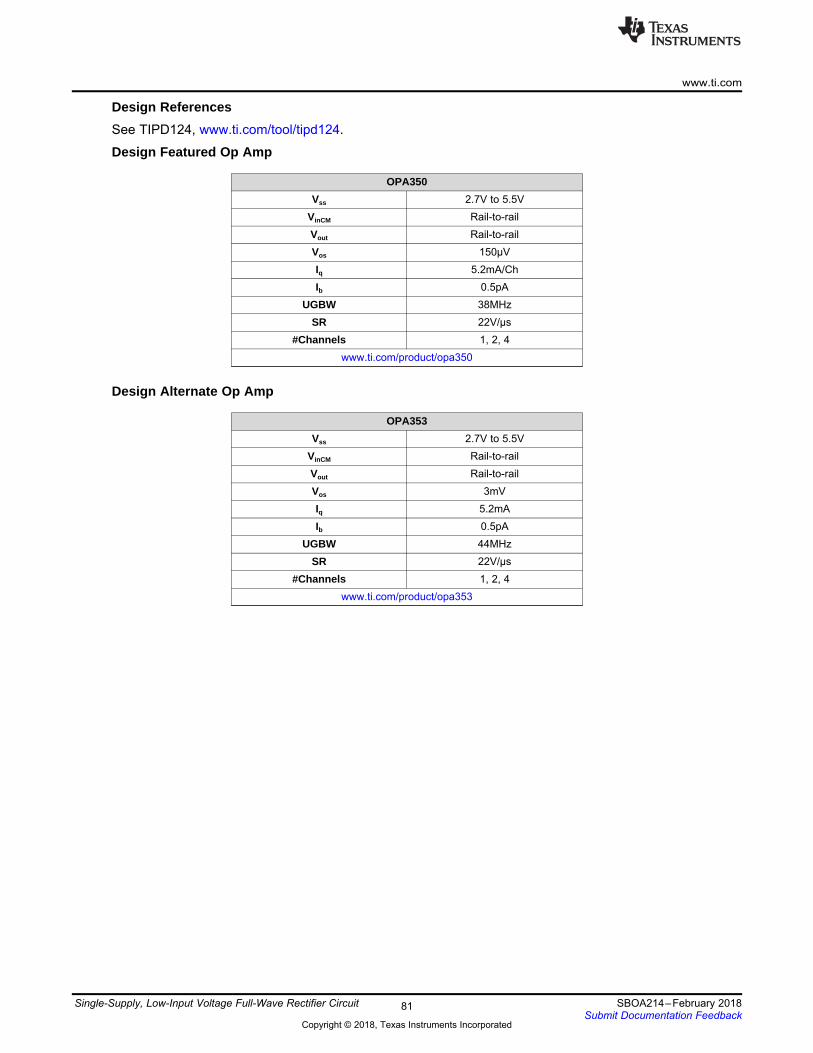
Design ReferencesSee TIPD124, www.ti.com/tool/tipd124.Design Featured Op Amp
OPA350Vss 2.7V to 5.5V
VinCM Rail-to-railVout Rail-to-railVos 150µVIq 5.2mA/ChIb 0.5pA
UGBW 38MHzSR 22V/µs
#Channels 1, 2, 4www.ti.com/product/opa350
Design Alternate Op Amp
OPA353Vss 2.7V to 5.5V
VinCM Rail-to-railVout Rail-to-railVos 3mVIq 5.2mAIb 0.5pA
UGBW 44MHzSR 22V/µs
#Channels 1, 2, 4www.ti.com/product/opa353
81

VeeVee
VccVcc
A+
IC1
Voa1
C1 470n R1 1.69k
RLoad 10k
+
-V+
U1 OPA192- U2 OPA192
Vo
R2 1.6MEG
Slew Rate LimiterOp Amp Gain Stage
Vee
Vcc
+
ViVee 15
Vcc 15
+V+
Copyright © 2018, Texas Instruments Incorporated
SBOA218–January 2018Submit Documentation Feedback
Copyright © 2018, Texas Instruments Incorporated
Slew Rate Limiter Circuit
Analog Engineer's Circuit: Op AmpsSBOA218–January 2018
Slew Rate Limiter Circuit
Design Goals
Input Output SupplyViMin ViMax VoMin VoMax Vcc Vee Vref
–10V 10V –10V 10V 15V –15V 0V
Design DescriptionThis circuit controls the slew rate of an analog gain stage. This circuit is intended for symmetrical slew rateapplications. The desired slew rate must be slower than that of the op amp chosen to implement the slewrate limiter.
Design Notes1. The gain stage op-amp and slew rate limiting op amp should both be checked for stability.2. Verify that the current demands for charging or discharging C1 plus any load current out of U2 will not
limit the voltage swing of U2.
82

www.ti.com
SBOA218–January 2018Submit Documentation Feedback
Copyright © 2018, Texas Instruments Incorporated
Slew Rate Limiter Circuit
Design Steps1. Set slew rate and choose a standard value for the feedback capacitor, C1.
2. Choose the value of R2 to set the capacitor current necessary for the desired slew rate.
3. Compensate feedback network for stability. R1 adds a pole to the 1/β network. This pole should beplaced so that the 1/β curve levels off a decade before it intersects the open loop gain curve (200Hz,for this example).
83

-3dB Frequency = 11.39kHz
Gai
n (d
B)
-50.00
-37.50
-25.00
-12.50
0.00
Frequency (Hz)10.00 100.00 1.00k 10.00k 100.00k 1.00MEG
Phas
e [d
eg]
-135.00
-101.25
-67.50
-33.75
0.00
-3dB Frequency = 11.39kHz
Time (s)0.00 2.75 5.50 8.25 11.00
IC1
-9.37u
9.37u
Vi
-10.00
10.00
Vo
-10.00
10.00
Voa1
-15.00
15.00
Slew Rate = 19.94V/s
www.ti.com
SBOA218–January 2018Submit Documentation Feedback
Copyright © 2018, Texas Instruments Incorporated
Slew Rate Limiter Circuit
Design SimulationsTransient Simulation Results
AC Simulation Results
84

www.ti.com
SBOA218–January 2018Submit Documentation Feedback
Copyright © 2018, Texas Instruments Incorporated
Slew Rate Limiter Circuit
Design ReferencesSee TIPD140, www.ti.com/tool/tipd140.
Design Featured Op Amp
OPA192Vcc 4.5V to 36V
VinCM Rail-to-railVout Rail-to-railVos 5µVIq 1mA/ChIb 5pA
UGBW 10MHzSR 20V/µs
#Channels 1, 2, 4www.ti.com/product/opa192
Design Alternate Op Amp
TLV2372Vcc 2.7V to 16V
VinCM Rail-to-railVout Rail-to-railVos 2mVIq 750µA/ChIb 1pA
UGBW 3MHzSR 2.1V/µs
#Channels 1, 2, 4www.ti.com/product/tlv2372
85
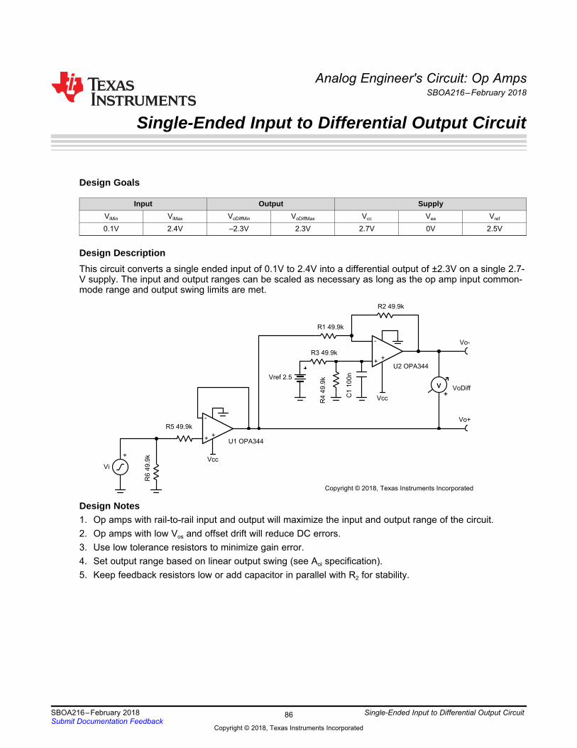
Vcc
Vcc
R3 49.9k
R4
49.9
kR1 49.9k
R2 49.9k
Vo+
Vo-
V+
VoDiffVref 2.5
R5 49.9k
C1
100n
+
-
+U1 OPA344
+
-
+U2 OPA344
R6
49.9
k+
Vi
Copyright © 2018, Texas Instruments Incorporated
SBOA216–February 2018Submit Documentation Feedback
Copyright © 2018, Texas Instruments Incorporated
Single-Ended Input to Differential Output Circuit
Analog Engineer's Circuit: Op AmpsSBOA216–February 2018
Single-Ended Input to Differential Output Circuit
Design Goals
Input Output SupplyViMin ViMax VoDiffMin VoDiffMax Vcc Vee Vref
0.1V 2.4V –2.3V 2.3V 2.7V 0V 2.5V
Design DescriptionThis circuit converts a single ended input of 0.1V to 2.4V into a differential output of ±2.3V on a single 2.7-V supply. The input and output ranges can be scaled as necessary as long as the op amp input common-mode range and output swing limits are met.
Design Notes1. Op amps with rail-to-rail input and output will maximize the input and output range of the circuit.2. Op amps with low Vos and offset drift will reduce DC errors.3. Use low tolerance resistors to minimize gain error.4. Set output range based on linear output swing (see Aol specification).5. Keep feedback resistors low or add capacitor in parallel with R2 for stability.
86

www.ti.com
SBOA216–February 2018Submit Documentation Feedback
Copyright © 2018, Texas Instruments Incorporated
Single-Ended Input to Differential Output Circuit
Design Steps1. Buffer Vi signal to generate Vo+.
2. Invert and level shift Vo+ using a difference amplifier to create Vo–.
3. Select resistances so that the resistor noise is smaller than the amplifier broadband noise.
4. Select resistances that protect the input of the amplifier and prevents floating inputs. To simplify the billof materials (BOM), select R5 = R6.
87

T
Frequency (Hz)10 100 1k 10k 100k 1MEG 10MEG
Gai
n(dB
)
-50
-40
-30
-20
-10
0
10
BW=690.7kHzG=6.02dB
VoDiff
T
Vi (V)100.00m 675.00m 1.25 1.83 2.40
VoD
iff(V
)
-2.30
-1.15
0.00
1.15
2.30
www.ti.com
SBOA216–February 2018Submit Documentation Feedback
Copyright © 2018, Texas Instruments Incorporated
Single-Ended Input to Differential Output Circuit
Design SimulationsDC Simulation Results
AC Simulation Results
88

www.ti.com
SBOA216–February 2018Submit Documentation Feedback
Copyright © 2018, Texas Instruments Incorporated
Single-Ended Input to Differential Output Circuit
Design ReferencesSee TIPD131, www.ti.com/tool/tipd131.Design Featured Op Amp
OPA344Vss 1.8V to 5.5V
VinCM Rail-to-railVout Rail-to-railVos 0.2mVIq 150µAIb 0.2pA
UGBW 1MHzSR 0.8V/µs
#Channels 1, 2, 4www.ti.com/product/opa344
Design Alternate Op Amp
OPA335Vss 2.7V to 5.5V
VinCM Vee–0.1V to Vcc–1.5VVout Rail-to-railVos 1µVIq 285µA/ChIb 70pA
UGBW 2MHzSR 1.6V/µs
#Channels 1, 2www.ti.com/product/opa335
89

Vcc 5
R1 845R2 1.04k
+
ViR3 5.56k
Vref 5 Vo-
++
U1 TLV9062
Copyright © 2018, Texas Instruments Incorporated
SBOA261–February 2018Submit Documentation Feedback
Copyright © 2018, Texas Instruments Incorporated
Inverting Op Amp With Inverting Positive Reference Voltage Circuit
Analog Engineer's Circuit: Op AmpsSBOA261–February 2018
Inverting Op Amp With Inverting Positive ReferenceVoltage Circuit
Design Goals
Input Output SupplyViMin ViMax VoMin VoMax Vcc Vee Vref
–5V –1V 0.05V 3.3V 5V 0V 5V
Design DescriptionThis design uses an inverting amplifier with an inverting positive reference to translate an input signal of–5V to –1V to an output voltage of 3.3V to 0.05V. This circuit can be used to translate a negative sensoroutput voltage to a usable ADC input voltage range.
Design Notes1. Use op amp linear output operating range. Usually specified under AOL test conditions.2. Common mode range must extend down to or below ground.3. Vref output must be low impedance.4. Input impedance of the circuit is equal to R2.5. Choose low-value resistors to use in the feedback. It is recommended to use resistor values less than
100kΩ. Using high-value resistors can degrade the phase margin of the amplifier and introduceadditional noise in the circuit.
6. The cutoff frequency of the circuit is dependent on the gain bandwidth product (GBP) of the amplifier.Additional filtering can be accomplished by adding a capacitor in parallel to R1. Adding a capacitor inparallel with R1 will also improve stability of the circuit if high-value resistors are used.
90

www.ti.com
Inverting Op Amp With Inverting Positive Reference Voltage Circuit SBOA261–February 2018Submit Documentation Feedback
Copyright © 2018, Texas Instruments Incorporated
Design Steps
1. Calculate the gain of the input signal.
2. Calculate R1 and R2.
3. Calculate the gain of the reference voltage required to offset the output.
4. Calculate R3.

Frequency (Hz)10 100 1k 10k 100k 1MEG 10MEG 100MEG
Gai
n (d
B)
-25
-20
-15
-10
-5
0
BW=7.25MHz
T
Input voltage (V)-5 -4 -3 -2 -1
Out
put V
olta
ge (V
)
50m
1.68
3.30
www.ti.com
SBOA261–February 2018Submit Documentation Feedback
Copyright © 2018, Texas Instruments Incorporated
Inverting Op Amp With Inverting Positive Reference Voltage Circuit
Design SimulationsDC Simulation Results
AC Simulation Results
92

www.ti.com
SBOA261–February 2018Submit Documentation Feedback
Copyright © 2018, Texas Instruments Incorporated
Inverting Op Amp With Inverting Positive Reference Voltage Circuit
Design ReferencesSee Designing Gain and Offset in Thirty Seconds.Design Featured Op Amp
TLV9062Vss 1.8V to 5.5V
VinCM Rail-to-railVout Rail-to-railVos 0.3mVIq 538µAIb 0.5pA
UGBW 10MHzSR 6.5V/µs
#Channels 1, 2, 4www.ti.com/product/tlv9062
Design Alternate Op Amp
OPA197Vss 4.5V to 36V
VinCM Rail-to-railVout Rail-to-railVos 25µVIq 1mAIb 5pA
UGBW 10MHzSR 20V/µs
#Channels 1, 2, 4www.ti.com/product/opa197
93

R1 1kR2 777
Vcc 5
Vref 2.5
+
Vi
VoR3 402
R4 1k
+
-
+U1 TSV912
Copyright © 2018, Texas Instruments Incorporated
SBOA262–February 2018Submit Documentation Feedback
Copyright © 2018, Texas Instruments Incorporated
Non-Inverting Op Amp With Inverting Positive Reference Voltage Circuit
Analog Engineer's Circuit: Op AmpsSBOA262–February 2018
Non-Inverting Op Amp With Inverting Positive ReferenceVoltage Circuit
Design Goals
Input Output SupplyViMin ViMax VoMin VoMax Vcc Vee Vref
2V 5V 0.05V 4.95V 5V 0V 2.5V
Design DescriptionThis design uses a non-inverting amplifier with an inverting positive reference to translate an input signalof 2V to 5V to an output voltage of 0.05V to 4.95V. This circuit can be used to translate a sensor outputvoltage with a positive slope and offset to a usable ADC input voltage range.
Design Notes1. Use op amp linear output operating range. Usually specified under AOL test conditions.2. Check op amp input common mode voltage range. The common mode voltage varies with the input
voltage.3. Vref must be low impedance.4. Input impedance of the circuit is equal to the sum of R3 and R4.5. Choose low-value resistors to use in the feedback. It is recommended to use resistor values less than
100kΩ. Using high-value resistors can degrade the phase margin of the amplifier and introduceadditional noise in the circuit.
6. The cutoff frequency of the circuit is dependent on the gain bandwidth product (GBP) of the amplifier.7. Adding a capacitor in parallel with R1 will improve stability of the circuit if high-value resistors are used.
94

www.ti.com
SBOA262–February 2018Submit Documentation Feedback
Copyright © 2018, Texas Instruments Incorporated
Non-Inverting Op Amp With Inverting Positive Reference Voltage Circuit
Design Steps
1. Calculate the gain of the input to produce the largest output swing.
2. Select a value for R1 and R4 and insert the values into the previous equation. The other two resistorvalues must be solved using a system of equations. The proper output swing and offset voltage cannotbe calculated if more than two variables are selected.
3. Solve the previous equation for R 3 in terms of R 2.
4. Select any point along the transfer function within the linear output range of the amplifier to set theproper offset voltage at the output (for example, the minimum input and output voltage).
5. Insert R3 from step 3 into the equation from step 4 and solve for R2.
6. Insert R2 calculation from step 5, and solve for R3.
95

Frequency (Hz)10 100 1k 10k 100k 1MEG 10MEG 100MEG
Gai
n (d
B)
-30
-25
-20
-15
-10
-5
0
5
BW=5.65MHz
Input voltage (V)2 3 4 5
Out
put V
olta
ge (V
)
50m
2.5
4.95
www.ti.com
SBOA262–February 2018Submit Documentation Feedback
Copyright © 2018, Texas Instruments Incorporated
Non-Inverting Op Amp With Inverting Positive Reference Voltage Circuit
Design SimulationsDC Simulation Results
AC Simulation Results
96

www.ti.com
SBOA262–February 2018Submit Documentation Feedback
Copyright © 2018, Texas Instruments Incorporated
Non-Inverting Op Amp With Inverting Positive Reference Voltage Circuit
Design ReferencesSee TI Precision Lab Videos on Input and Output Limitations.Design Featured Op Amp
TSV912Vss 2.5V to 5.5V
VinCM Rail-to-railVout Rail-to-railVos 0.3mVIq 550µAIb 1pA
UGBW 8MHzSR 4.5V/µs
#Channels 1, 2, 4www.ti.com/product/tsv912
Design Alternate Op Amp
OPA191Vss 4.5V to 36V
VinCM Rail-to-railVout Rail-to-railVos 5µVIq 140µA/ChIb 5pA
UGBW 2.5MHzSR 5.5V/µs
#Channels 1, 2, 4www.ti.com/product/opa191
97

R1 1k
Vcc 5
R3 412
+
ViR4 1k
Vref 2.5
R2 1.37k
Vo-
++
U1 MCP6292
Copyright © 2018, Texas Instruments Incorporated
SBOA263–January 2018Submit Documentation Feedback
Copyright © 2018, Texas Instruments Incorporated
Non-Inverting Op Amp With Non-Inverting Positive Reference Voltage Circuit
Analog Engineer's Circuit: Op AmpsSBOA263–January 2018
Non-Inverting Op Amp With Non-Inverting PositiveReference Voltage Circuit
Design Goals
Input Output SupplyViMin ViMax VoMin VoMax Vcc Vee Vref
–1V 3V 0.05V 4.95V 5V 0V 2.5V
Design DescriptionThis design uses a non-inverting amplifier with a non-inverting positive reference to translate an inputsignal of –1V to 3V to an output voltage of 0.05V to 4.95V. This circuit can be used to translate a sensoroutput voltage with a positive slope and negative offset to a usable ADC input voltage range.
Design Notes1. Use op amp linear output operating range. Usually specified under AOL test conditions.2. Check op amp input common mode voltage range.3. Vref output must be low impedance.4. Input impedance of the circuit is equal to the sum of R3 and R4.5. Choose low-value resistors to use in the feedback. It is recommended to use resistor values less than
100kΩ. Using high-value resistors can degrade the phase margin of the amplifier and introduceadditional noise in the circuit.
6. The cutoff frequency of the circuit is dependent on the gain bandwidth product (GBP) of the amplifier.7. Adding a capacitor in parallel with R1 will improve stability of the circuit if high-value resistors are used.
98

www.ti.com
SBOA263–January 2018Submit Documentation Feedback
Copyright © 2018, Texas Instruments Incorporated
Non-Inverting Op Amp With Non-Inverting Positive Reference Voltage Circuit
Design Steps
1. Calculate the gain of the input voltage to produce the desired output swing.
2. Select a value for R1 and R4 and insert the values into the previous equation. The other two resistorvalues must be solved using a system of equations. The proper output swing and offset voltage cannotbe calculated if more than two variables are selected.
3. Solve the previous equation for R3 in terms of R2.
4. Select any point along the transfer function within the linear output range of the amplifier to set theproper offset voltage at the output (for example, the minimum input and output voltage).
5. Insert R3 into the equation from step 1 and solve for R2.
6. Insert R2 into the equation from step 1 to solve for R3.
99

T
Frequency (Hz)1 10 100 1k 10k 100k 1MEG 10MEG 100MEG
Gai
n (d
B)
-25
-20
-15
-10
-5
0
5
BW=9.01MHz
T
Input voltage (V)
-1 0 1 2 3
Ou
tpu
t V
olt
age
(V)
50m
2.5
4.95
www.ti.com
SBOA263–January 2018Submit Documentation Feedback
Copyright © 2018, Texas Instruments Incorporated
Non-Inverting Op Amp With Non-Inverting Positive Reference Voltage Circuit
Design SimulationsDC Simulation Results
AC Simulation Results
100

www.ti.com
SBOA263–January 2018Submit Documentation Feedback
Copyright © 2018, Texas Instruments Incorporated
Non-Inverting Op Amp With Non-Inverting Positive Reference Voltage Circuit
Design ReferencesSee Designing Gain and Offset in Thirty Seconds.Design Featured Op Amp
MCP6292Vss 2.4V to 5.5V
VinCM Rail-to-railVout Rail-to-railVos 0.3mVIq 600µAIb 1pA
UGBW 10MHzSR 6.5V/µs
#Channels 1, 2, 4www.ti.com/product/MCP6292
Design Alternate Op Amp
OPA388Vss 2.5V to 5.5V
VinCM Rail-to-railVout Rail-to-railVos 0.25µVIq 1.9mAIb 30pA
UGBW 10MHzSR 5V/µs
#Channels 1, 2, 4www.ti.com/product/opa388
101

VCC 5
R1 11.1kR2 6.81k
Vo
Vref 1.259
+
Vi
-
++
U1 TLV9001
Copyright © 2018, Texas Instruments Incorporated
SBOA264–February 2018Submit Documentation Feedback
Copyright © 2018, Texas Instruments Incorporated
Inverting Op Amp With Non-Inverting Positive Reference Voltage Circuit
Analog Engineer's Circuit: Op AmpsSBOA264–February 2018
Inverting Op Amp With Non-Inverting Positive ReferenceVoltage Circuit
Design Goals
Input Output SupplyViMin ViMax VoMin VoMax Vcc Vee Vref
–1V 2V 0.05V 4.95V 5V 0V 1.259V
Design DescriptionThis design uses an inverting amplifier with a non-inverting positive reference voltage to translate an inputsignal of –1V to 2V to an output voltage of 0.05V to 4.95V. This circuit can be used to translate a sensoroutput voltage with a positive slope and negative offset to a usable ADC input voltage range.
Design Notes1. Use op amp linear output operating range. Usually specified under AOL test conditions.2. Amplifier common mode voltage is equal to the reference voltage.3. Vref can be created with a voltage divider.4. Input impedance of the circuit is equal to R2.5. Choose low-value resistors to use in the feedback. It is recommended to use resistor values less than
100kΩ. Using high-value resistors can degrade the phase margin of the amplifier and introduceadditional noise in the circuit.
6. The cutoff frequency of the circuit is dependent on the gain bandwidth product (GBP) of the amplifier.Additional filtering can be accomplished by adding a capacitor in parallel to R1. Adding a capacitor inparallel with R1 will also improve stability of the circuit, if high-value resistors are used.
102

www.ti.com
SBOA264–February 2018Submit Documentation Feedback
Copyright © 2018, Texas Instruments Incorporated
Inverting Op Amp With Non-Inverting Positive Reference Voltage Circuit
Design Steps
1. Calculate the gain of the input signal.
2. Select R2 and calculate R1.
3. Calculate the reference voltage.
103

T
Frequency (Hz)1 10 100 1k 10k 100k 1MEG 10MEG
Gai
n (d
B)
-25
-20
-15
-10
-5
0
5
BW = 590kHz
T
Input voltage (V)-1 0 1 2
Out
put V
olta
ge (V
)
50m
2.5
4.95
www.ti.com
SBOA264–February 2018Submit Documentation Feedback
Copyright © 2018, Texas Instruments Incorporated
Inverting Op Amp With Non-Inverting Positive Reference Voltage Circuit
Design SimulationsDC Simulation Results
AC Simulation Results
104

www.ti.com
SBOA264–February 2018Submit Documentation Feedback
Copyright © 2018, Texas Instruments Incorporated
Inverting Op Amp With Non-Inverting Positive Reference Voltage Circuit
Design ReferencesSee Designing Gain and Offset in Thirty Seconds.Design Featured Op Amp
TLV9001Vss 1.8V to 5.5V
VinCM Rail-to-railVout Rail-to-railVos 0.4mVIq 60µAIb 5pA
UGBW 1MHzSR 2V/µs
#Channels 1, 2, 4www.ti.com/product/tlv9002
Design Alternate Op Amp
OPA376Vss 2.2V to 5.5V
VinCM Rail-to-railVout Rail-to-railVos 5µVIq 760µAIb 0.2pA
UGBW 5.5MHzSR 2V/µs
#Channels 1, 2, 4www.ti.com/product/opa376
105

Vcc 5VVref 5V
Vcc 5V
Vref 5V
Vee 0V Vee 0V
R3
576k
R1
100k
R2
100k
Vo1
Vi
+
VtriangleR4
100k
R5
100k
Vo2
-
+
U1
TLV3201-
+U2 TLV3201+
Vnoise
Comparator With Hysteresis Comparator Without Hysteresis
Copyright © 2018, Texas Instruments Incorporated
SBOA219–January 2018Submit Documentation Feedback
Copyright © 2018, Texas Instruments Incorporated
Comparator With and Without Hysteresis Circuit
Analog Engineer's Circuit: Op AmpsSBOA219–January 2018
Comparator With and Without Hysteresis Circuit
Design Goals
Input Output SupplyViMin ViMax VoMin VoMax Vcc Vee Vref
0V 5V 0V 5V 5V 0V 5V
VL (Lower Threshold) VH (Upper Threshold) VH – VL
2.3V 2.7V 0.4V
Design DescriptionComparators are used to compare two different signal levels and create an output based on the input withthe higher input voltage. Noise or signal variation at the comparison threshold will cause the comparatoroutput to have multiple output transitions. Hysteresis sets upper- and lower-threshold voltages to eliminatethe multiple transitions caused by noise.
Design Notes1. Use a comparator with low quiescent current to reduce power consumption.2. The accuracy of the hysteresis threshold voltages are related to the tolerance of the resistors used in
the circuit.3. The propagation delay is based on the specifications of the selected comparator.
106

www.ti.com
SBOA219–January 2018Submit Documentation Feedback
Copyright © 2018, Texas Instruments Incorporated
Comparator With and Without Hysteresis Circuit
Design Steps1. Select components for the comparator with hysteresis.
a. Select VL, VH, and R1.
b. Calculate R2.
c. Calculate R3.
d. Verify hysteresis width.
2. Select components for comparator without hysteresis.a. Select Vth and R4 .
b. Calculate R5.
107

T
Time (s)
40u 57u 75u 92u 110u
Vo1
0
5
Vi
2.3
2.5
2.7
Vo2
0
5
T
Vo1->5V @ Vi < 2.3V
Time (s)
0 100u 200u 300u
Vo1
0
5
Vi
0
5
Vo2
0
5
Vo1�5V @ Vi < 2.3V
Vo1�0V @ Vi > 2.7V
Vo2�5V @ Vi < 2.5V
Vo2�0V @ Vi > 2.5V
www.ti.com
SBOA219–January 2018Submit Documentation Feedback
Copyright © 2018, Texas Instruments Incorporated
Comparator With and Without Hysteresis Circuit
Design SimulationsTransient Simulation Results
Noise Only Present From 0s to 120µs
Zoomed in From 40µs to 110µs
108
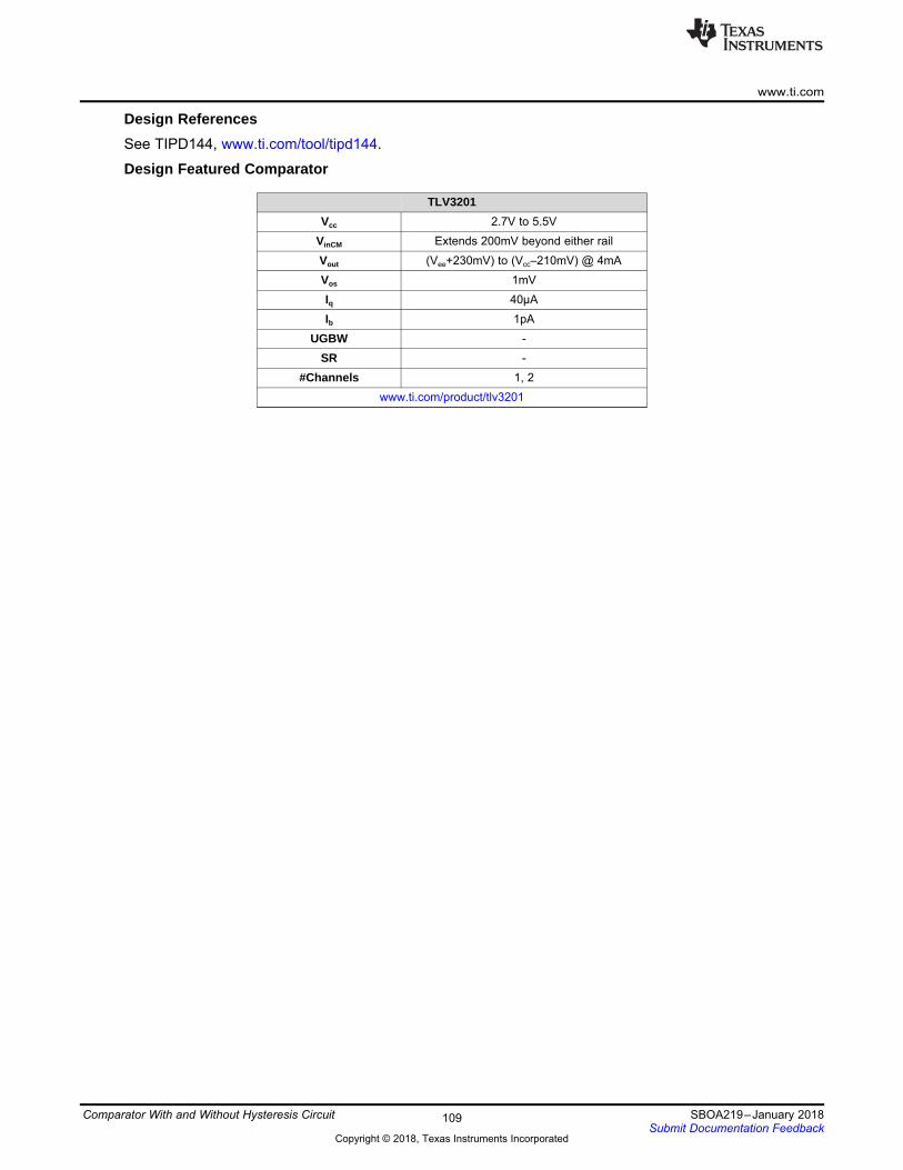
www.ti.com
SBOA219–January 2018Submit Documentation Feedback
Copyright © 2018, Texas Instruments Incorporated
Comparator With and Without Hysteresis Circuit
Design ReferencesSee TIPD144, www.ti.com/tool/tipd144.Design Featured Comparator
TLV3201Vcc 2.7V to 5.5V
VinCM Extends 200mV beyond either railVout (Vee+230mV) to (Vcc–210mV) @ 4mAVos 1mVIq 40µAIb 1pA
UGBW -SR -
#Channels 1, 2www.ti.com/product/tlv3201
109

Vref
Vcc
Vpu
Vcc
Vcc
VpuVcc
Vi
Vref 2.5
+
Vtri
Vh
R3 10k
R2 10k
Vpu 10
-
+
+
U1 TLV1701
-
+
+
U2 TLV1701
Vcc 5
Vo
Rp 5.1k
TLV1702
VrefVl
R1 10k
Copyright © 2018, Texas Instruments Incorporated
SBOA221–January 2018Submit Documentation Feedback
Copyright © 2018, Texas Instruments Incorporated
Window Comparator Circuit
Analog Engineer's Circuit: Op AmpsSBOA221–January 2018
Window Comparator Circuit
Design Goals
Input Output SupplyViMin ViMax VoMin VoMax Vcc Vee Vref
0V 5V 0V 36V 5V 0V 2.5V
VL (Lower Threshold) VH (Upper Threshold) Upper to Lower Threshold Ratio1.66V 3.33V 2
Design DescriptionThis circuit utilizes two comparators in parallel to determine if a signal is between two reference voltages.If the signal is within the window, the output is high. If the signal level is outside of the window, the outputis low. For this design, the reference voltages are generated from a single supply with voltage dividers.
Design Notes1. The input should not exceed the common mode limitations of the comparators.2. If higher pullup voltages are used, Rp should be sized accordingly to prevent large current draw. The
TLV1701 supports pullup voltages up to 36V.3. Comparator must be open-drain or open-collector to allow for the ORed output.
110

Vh
Vi
Vl
Vo
Time (s)0.00 10.00m 20.00m
Out
put V
olta
ge (V
)
0.00
2.50
5.00
7.50
10.00
Vi
Vl
Vh
Vo
www.ti.com
SBOA221–January 2018Submit Documentation Feedback
Copyright © 2018, Texas Instruments Incorporated
Window Comparator Circuit
Design Steps1. Define the upper (VH) and lower (VL) window voltages.
2. Choose resistor values to achieve the desired window voltages.
Design SimulationsTransient Simulation Results
111

www.ti.com
SBOA221–January 2018Submit Documentation Feedback
Copyright © 2018, Texas Instruments Incorporated
Window Comparator Circuit
Design ReferencesSee TIPD178, www.ti.com/tool/tipd178.Design Featured Op Amp
TLV1702Vcc 2.2V to 36V
VinCM Rail-to-railVout Open Collector (36V Max)Vos 2.5mVIq 75µA/ChIb 15nA
Rise Time 365nsFall Time 240ns
#Channels 1, 2, 4www.ti.com/product/tlv1702
112

SBOA220–January 2018Submit Documentation Feedback
Copyright © 2018, Texas Instruments Incorporated
Photodiode Amplifier Circuit
Analog Engineer's Circuit: Op AmpsSBOA220–January 2018
Photodiode Amplifier Circuit
Design Goals
Input Output BW SupplyIiMin IiMax VoMin VoMax fp Vcc Vee Vref
0A 2.4µA 100mV 4.9V 20kHz 5V 0V 0.1V
Design DescriptionThis circuit consists of an op amp configured as a transimpedance amplifier for amplifying the light-dependent current of a photodiode.
Design Notes1. A bias voltage (Vref) prevents the output from saturating at the negative power supply rail when the
input current is 0A.2. Use a JFET or CMOS input op amp with low bias current to reduce DC errors.3. Set output range based on linear output swing (see Aol specification).
113

www.ti.com
Photodiode Amplifier Circuit SBOA220–January2018Submit Documentation Feedback
Copyright © 2018, Texas Instruments Incorporated
Design Steps1. Select the gain resistor.
2. Select the feedback capacitor to meet the circuit bandwidth.
3. Calculate the necessary op amp gain bandwidth (GBW) for the circuit to be stable.
• Cj: Junction capacitance of photodiode• Cd: Differential input capacitance of the amplifier• Ccm: Common-mode input capacitance of the inverting input
4. Calculate the bias network for a 0.1-V bias voltage.
5. Select C2 to be 1µF to filter the Vref voltage. The resulting cutoff frequency is:

www.ti.com
SBOA220–January 2018Submit Documentation Feedback
Copyright © 2018, Texas Instruments Incorporated
Photodiode Amplifier Circuit
Design SimulationsDC Simulation Results
AC Simulation Results
115

www.ti.com
SBOA220–January 2018Submit Documentation Feedback
Copyright © 2018, Texas Instruments Incorporated
Photodiode Amplifier Circuit
Design ReferencesSee TIPD176, www.ti.com/tool/tipd176.
Design Featured Op Amp
OPA322Vcc 1.8V to 5.5V
VinCM Rail–to–railVout Rail–to–railVos 0.5mVIq 1.6mA/ChIb 0.2pA
UGBW 20MHzSR 10V/µs
#Channels 1, 2, 4www.ti.com/product/opa322
Design Alternate Op Amp
LMP7721Vcc 1.8V to 5.5V
VinCM Vee to (Vcc –1V)Vout Rail–to–railVos 26µVIq 1.3mA/ChIb 3fA
UGBW 17MHzSR 10.43V/µs
#Channels 1www.ti.com/product/lmp7721
116

IMPORTANT NOTICE FOR TI DESIGN INFORMATION AND RESOURCES
Texas Instruments Incorporated (‘TI”) technical, application or other design advice, services or information, including, but not limited to,reference designs and materials relating to evaluation modules, (collectively, “TI Resources”) are intended to assist designers who aredeveloping applications that incorporate TI products; by downloading, accessing or using any particular TI Resource in any way, you(individually or, if you are acting on behalf of a company, your company) agree to use it solely for this purpose and subject to the terms ofthis Notice.TI’s provision of TI Resources does not expand or otherwise alter TI’s applicable published warranties or warranty disclaimers for TIproducts, and no additional obligations or liabilities arise from TI providing such TI Resources. TI reserves the right to make corrections,enhancements, improvements and other changes to its TI Resources.You understand and agree that you remain responsible for using your independent analysis, evaluation and judgment in designing yourapplications and that you have full and exclusive responsibility to assure the safety of your applications and compliance of your applications(and of all TI products used in or for your applications) with all applicable regulations, laws and other applicable requirements. Yourepresent that, with respect to your applications, you have all the necessary expertise to create and implement safeguards that (1)anticipate dangerous consequences of failures, (2) monitor failures and their consequences, and (3) lessen the likelihood of failures thatmight cause harm and take appropriate actions. You agree that prior to using or distributing any applications that include TI products, youwill thoroughly test such applications and the functionality of such TI products as used in such applications. TI has not conducted anytesting other than that specifically described in the published documentation for a particular TI Resource.You are authorized to use, copy and modify any individual TI Resource only in connection with the development of applications that includethe TI product(s) identified in such TI Resource. NO OTHER LICENSE, EXPRESS OR IMPLIED, BY ESTOPPEL OR OTHERWISE TOANY OTHER TI INTELLECTUAL PROPERTY RIGHT, AND NO LICENSE TO ANY TECHNOLOGY OR INTELLECTUAL PROPERTYRIGHT OF TI OR ANY THIRD PARTY IS GRANTED HEREIN, including but not limited to any patent right, copyright, mask work right, orother intellectual property right relating to any combination, machine, or process in which TI products or services are used. Informationregarding or referencing third-party products or services does not constitute a license to use such products or services, or a warranty orendorsement thereof. Use of TI Resources may require a license from a third party under the patents or other intellectual property of thethird party, or a license from TI under the patents or other intellectual property of TI.TI RESOURCES ARE PROVIDED “AS IS” AND WITH ALL FAULTS. TI DISCLAIMS ALL OTHER WARRANTIES ORREPRESENTATIONS, EXPRESS OR IMPLIED, REGARDING TI RESOURCES OR USE THEREOF, INCLUDING BUT NOT LIMITED TOACCURACY OR COMPLETENESS, TITLE, ANY EPIDEMIC FAILURE WARRANTY AND ANY IMPLIED WARRANTIES OFMERCHANTABILITY, FITNESS FOR A PARTICULAR PURPOSE, AND NON-INFRINGEMENT OF ANY THIRD PARTY INTELLECTUALPROPERTY RIGHTS.TI SHALL NOT BE LIABLE FOR AND SHALL NOT DEFEND OR INDEMNIFY YOU AGAINST ANY CLAIM, INCLUDING BUT NOTLIMITED TO ANY INFRINGEMENT CLAIM THAT RELATES TO OR IS BASED ON ANY COMBINATION OF PRODUCTS EVEN IFDESCRIBED IN TI RESOURCES OR OTHERWISE. IN NO EVENT SHALL TI BE LIABLE FOR ANY ACTUAL, DIRECT, SPECIAL,COLLATERAL, INDIRECT, PUNITIVE, INCIDENTAL, CONSEQUENTIAL OR EXEMPLARY DAMAGES IN CONNECTION WITH ORARISING OUT OF TI RESOURCES OR USE THEREOF, AND REGARDLESS OF WHETHER TI HAS BEEN ADVISED OF THEPOSSIBILITY OF SUCH DAMAGES.You agree to fully indemnify TI and its representatives against any damages, costs, losses, and/or liabilities arising out of your non-compliance with the terms and provisions of this Notice.This Notice applies to TI Resources. Additional terms apply to the use and purchase of certain types of materials, TI products and services.These include; without limitation, TI’s standard terms for semiconductor products http://www.ti.com/sc/docs/stdterms.htm), evaluationmodules, and samples (http://www.ti.com/sc/docs/sampterms.htm).
Mailing Address: Texas Instruments, Post Office Box 655303, Dallas, Texas 75265Copyright © 2018, Texas Instruments Incorporated