analog electronic circuits code:...
TRANSCRIPT

Analog Electronic CircuitsCode: EE-305-F
1

Section -COperational Amplifier
INTRODUCTION •• UsuallyUsually CalledCalled OpOp AmpsAmps
•• AnAn amplifieramplifier isis aa devicedevice thatthat acceptsaccepts aa varyingvarying inputinput signalsignal andand producesproduces aa similarsimilaroutputoutput signalsignal withwith aa largerlarger amplitudeamplitude..
•• UsuallyUsually connectedconnected soso partpart ofof thethe outputoutput isis fedfed backback toto thethe inputinput.. (Feedback(Feedback Loop)Loop)
•• MostMost OpOp AmpsAmps behavebehave likelike voltagevoltage amplifiersamplifiers.. TheyThey taketake anan inputinput voltagevoltage andand outputoutput aascaledscaled versionversion..
•• TheyThey areare thethe basicbasic componentscomponents usedused toto buildbuild analoganalog circuitscircuits..
•• TheThe namename “operational“operational amplifier”amplifier” comescomes fromfrom thethe factfact thatthat theythey werewere originallyoriginally usedusedtoto performperform mathematicalmathematical operationsoperations suchsuch asas integrationintegration andand differentiationdifferentiation..
WeWe cancan saysay::
OperationalOperational amplifieramplifier isis aa directdirect coupledcoupled highhigh gaingain amplifieramplifier toto whichwhich feedbackfeedback isisaddedadded toto controlcontrol itsits overalloverall responseresponse characteristiccharacteristic.. ItIt isis usedused toto performperform widewide varietyvarietyofof linearlinear andand nonnon linearlinear functionfunction andand isis oftenoften referredreferred toto asas basicbasic linearlinear integratedintegratedcircuitcircuit oror moremore accuratelyaccurately analoganalog integratedintegrated circuitcircuit..
2

Block Diagram of typical Op-amp
Input Stage
Intermediate Stage
Level Shifting stage
Output stage
Non inverting input
Inverting input
output
Dual-input Dual-input such as emitter complementaryBalanced output unbalanced o/p follower using symmetry pushDifferential amp. Differential amp. Constant current pull amplifier
source
3

Schematic Symbol
Op-amp has two inputs that connect to two terminals and one output
Input1- non inverting input (volts)Input2- inverting input (volts)Output- output voltage (volts)A-Large signal voltage gain
Output= A (input1-input2)
A
4

Equivalent circuit of an op-amp
•• ii(+)(+),, ii((--)) :: CurrentsCurrents intointo thethe amplifieramplifier onon thethe invertinginverting andand noninvertingnoninverting lineslinesrespectivelyrespectively
•• vvidid :: TheThe inputinput voltagevoltage fromfrom invertinginverting toto nonnon--invertinginverting inputsinputs•• ++VVcccc ,, --VVEEEE :: DCDC sourcesource voltages,voltages, usuallyusually ++1515VV andand ––1515VV• Zin :: TheThe inputinput resistance,resistance, ideallyideally infinityinfinity•• AA :: TheThe gaingain ofof thethe amplifieramplifier.. IdeallyIdeally veryvery high,high, inin thethe 11xx10101010 rangerange..•• ZZOutOut:: TheThe outputoutput resistance,resistance, ideallyideally zerozero•• vvOO:: TheThe outputoutput voltagevoltage;; vvOO == AAOLOLvvidid wherewhere AAOLOL isis thethe openopen--looploop voltagevoltage gaingain•• VVidid:: DifferenceDifference inputinput voltagevoltage
--VVEEEE
vvidid
InvertingInverting
NoninvertingNoninverting
OutputOutput
++
__ii((--))
ii(+)(+)
vvOO = = AAddvvidid
ZZOutOut
AAZin
++VVcccc
5

Schematic diagram of 741 IC opamp
6

Dual –in-line package
7
Since the op-amp is the differential type, input offset voltage must be controlled soas to minimize offset. Offset voltage is nulled by application of a voltage of oppositepolarity to the offset. An offset null-adjustment potentiometer may be used tocompensate for offset voltage. The null-offset potentiometer also compensates forirregularities in the operational amplifier manufacturing process which may cause anoffset.

Ideal Voltage transfer curve of op amp
vvOO == AAOLOLvvidid This is the basic op-amp equation in which the output offset voltage is assumedto be zero.The graphic representation of this equation is shown; where the output voltage ,Vo is plottedagainst input difference voltage Vid,keeping gain A constant.The output voltage cannot exceed the positive and negative saturation voltage.The output voltage is directly proportional to the input difference voltage until it reaches thesaturation voltages and thereafter the output voltage remains constant.This curve is called ideal voltage transfer curve.
8

Ideal Vs Practical Op-Amp
Ideal Practical
Open Loop gain A 105
Bandwidth BW 10-100Hz
Input Impedance Zin >1M
Output Impedance Zout 0 10-100
Output Voltage Vout Depends only on Vd = (V+V)Differential mode signal
Depends slightly on average input Vc = (V++V)/2 Common-Mode signal
CMRR 10-100dB
+
~
AVin
Vin Vout
Zout=0
Ideal op-amp
+
AVin
Vin Vout
Zout
~Zin
Practical op-amp
9

Open loop op-amp configuration• In case of amplifiers the term open loop indicates that no
connection either direct or via another network exists between input and output terminals.
• Output signal is not fed back in any form as part of input signal.• When connected in open loop configuration, the op-amp simply
function as high-gain amplifier. There are 3 open loop op amp configuration:
1) Differential amplifier2) Inverting amplifier3) Non inverting amplifier
These configuration are classed according to number of inputs used and the terminal to which input as applied when a single input is used.
10

The Differential Amplifier
• open loop differential amplifier in which input signals vin1 and vin2 are applied to the positive and negative input terminals.
• Since the OPAMP amplifies the difference the between the two input signals, this configuration is called the differential amplifier.
• The OPAMP amplifies both ac and dc input signals. The source resistance Rin1 and Rin2 are normally negligible compared to the input resistance Ri (ideally infinite). Therefore voltage drop across these resistances can be assumed to be zero.
• Therefore• v1 = vin1 and v2 = vin2.• vo = Ad (vin1 – vin2 )• where, Ad is the open loop gain.
11

The Inverting Amplifier
• If the input is applied to only inverting terminal and non-inverting terminal is grounded then it is called inverting amplifier. This configuration is shown in fig.
• v1= 0, v2 = vin.
• vo = -Ad vin
• The negative sign indicates that the output voltage is out of phase with respect to input 180 °or is of opposite polarity. Thus the input signal is amplified and inverted also.
12

The Non-inverting Amplifier
• In this configuration, the input voltage is applied to non-inverting terminals and inverting terminal is ground as shown in fig.
• v1 = +vin v2 = 0• vo = +Ad vin
• This means that the input voltage is amplified by Ad and there is no phase reversal at the output.
• In all three configurations any input signal slightly greater than zero drive the output to saturation level. This is because of very high gain. Thus when operated in open-loop, the output of the OPAMP is either negative or positive saturation or switches between positive and negative saturation levels. Therefore open loop op-amp is not used in linear applications.
13

Open loop op amp is not used in linear applications. Why?
Because open loop gain of op amp is very high, only the smaller signals (on order of microvolt or less) having very low frequency may be amplified accurately without distortion. These small signals are very susceptible to noise and almost impossible to obtain in lab.
Open loop voltage gain of op amp is not constant and varies with change in temperature and power supply. These variations makes the open loop op amp unsuitable for many linear applications.
So open loop op amp is impractical in ac applications. For e.g. open loop bandwidth of 741C is approx. 5Hz. In almost all ac applications a bandwidth larger than 5Hz is needed.
So to select as well as control the gain of op amp , add feedback in the circuit ,means output signal is fed back to the input either directly or via another network.
14

Types of feed back• Negative feedback: If the signal fed back is of opposite polarity or out of phase by
180◦ (or odd integer multiple of 180◦) with respect to input signal, feedback iscalled negative feedback.
• –ve feedback is also known as degenerative feedback because when used itdegenerates (reduces)the output voltage amplitude and in turn reduces thevoltage gain.
Uses:
• When used in amplifier,-ve feedback stabilizes the gain, increases the bandwidthand changes the input and output resistances, reduced voltage gain, decrease innon linear distortion and reduces the effect of variations in temperature andsupply voltages on the output of op-amp.
• Positive feedback: If the signal fed back is of the same polarity or in phase withthe input signal, the feedback is called positive feedback.
• In + ve feedback the feedback signal aids the input signal, so referred asregenerative feedback. +ve feedback is used in oscillator circuits.
15

A op amp that uses feedback is called feedback amplifier.
Feedback forms a close loop between input and output so referred as closed loop amplifier also.
Feedback amplifier consists of two parts: op-amp and feedback circuit (made up of either passive ,active or combination of both components)
There are four ways to connect these 2 blocks according to whether the voltage or current is fed back to the input in series or in parallel:-
1) Voltage series feedback The voltage across RL is input voltage to feedback circuit. Feedback
2) Voltage shunt feedback quantity is the output of feedback circuit and proportional to output voltage.
3) Current series feedback Load current flows into feedback circuit . Output of feedback circuit
4) Current shunt feedback (either current or voltage) is proportional to load current.
16

RL
Fig. A voltage-seriesFig. B voltage-shunt
Fig. C current-series Fig. D current-shunt
RL
17

Voltage series feedback amplifier or non inverting amplifier with feedback
+
-
18

Calculations• Negative feedback vid=Vin-Vf
• Closed loop voltage gain Af=A/(1+AB)
• Difference input voltage Af=1+ Rf/R1
• Bandwidth with feedback Ff=fo(1+AB)
• Total output offset voltage with feedback=
(Total output offset voltage without feedback)/(1+AB)
19
Open loop gain vs. freq .response

Input and output resistance with feedback
20
Input resistance with feedback Rif=Ri(1+AB)Output Resistance with feedback Rof =Ro/(1+AB)
Rif
Rof
BACK

Op-amp Voltage Follower Configuration• The lowest gain that can be obtained from a non
inverting amplifier with feedback is 1.• When non inverting amplifier is configured for unity
gain , it is called voltage follower because the o/p voltage is equal to and in phase with the input or output follows the input.
• The op-amp configuration shown at left is a voltage-follower often used as a buffer amplifier– Output is connected directly to negative input (negative
feedback)– Since v+ = v- = vIN, and vOUT = v-, so closed-loop gain Ao =
1– We can obtain the same result by writing
vOUT = A (vIN – vOUT) or vOUT/vIN = A/(1 + A) = 1 for A >> 1
• A typical voltage-follower transfer curve is shown in the left-bottom figure for the case VPOS = +15V and VNEG = -10V– For vIN between –10 and +15 volts, vOUT = vIN
– If vIN exceeds +15V, the output saturates at VPOS
– If vIN < -10V, the output saturates at VNEG
21
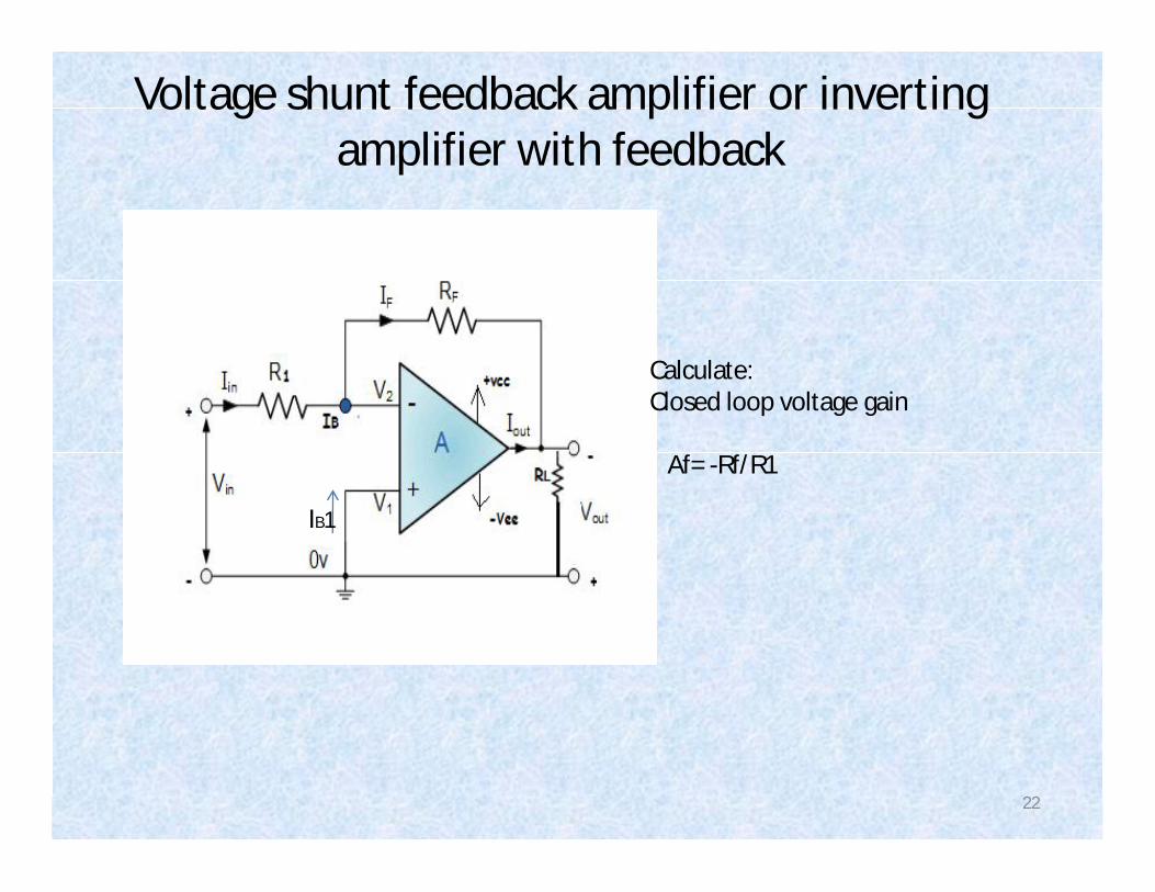
Voltage shunt feedback amplifier or inverting amplifier with feedback
Calculate:Closed loop voltage gain
Af= -Rf/R1
22
IB1