analog cmos interface circuits for umsi chip of ... · pdf fileanalog cmos interface circuits...
TRANSCRIPT

Analog CMOS Interface Circuits for UMSI Chipof Environmental Monitoring Microsystem
A report Submitted to Canopus Systems Inc.
Zuhail Sainudeen and Navid Yazdi
Arizona State University
July 2001

2
1. Overview
The objective of this project has been to implement the analog interface circuitry of the UMSI chip for theEnvironmental Monitoring Microsystem. This circuitry provides the readout for capacitive sensors, a resistivesensor, and interface for sensors with direct voltage output. The analog interface circuit block is highlyprogrammable and provides offset and gain adjustments. It also supports self-test for physical capacitivesensors. This report describes the general architecture and detailed description of the design. Also simulatedperformance of the circuit is presented.
2. General Architecture
The overall architecture of the interface is shown in Fig 1. The circuit uses 6-to-1 input multipplexer tointerface with up to 6 capacitive sensors, 6 resistive sensors, and 6 sensors with direct voltage output .
Fig. 1: Overall architecture of the UMSI chip analog interface.
3
Each of the individual readout blocks develops an output voltage proportional to the input parameter. Thecapacitive readout develops a voltage proportional to the difference in capacitance between a ‘sense’ capacitorand a reference capacitor. Similarly, the resistive sensor readout interfaces with a resistive sensor half or fullbridge, and provides an output corresponding to the bridge resistor change. The voltage readout stageattenuates the input voltage change to a desired range. The output from the readout blocks is fed, via amultiplexer to a gain stage, which amplifies the input signal by a programmable factor to accommodatesensors with various sensitivities. The multiplexer allows output selected from any of the readout circuits tobe amplified by the gain stage. The output voltage of this stage is finally stored on a capacitor in the sampledand hold stage
Additionally, there is a 6-bit DAC, or digital to analog converter, which is used to generate voltage Vp andVref. The voltage Vref is applied to the capacitive sensor readout, programmable gain amplifier, and sampleand hold stage so as to cancel any ‘offset’. Offset is a non-ideality where there is an output signal present inthe absence of any input signal. The voltage Vp is used for self-test of the physical capacitive sensor. Selftest is performed by applying a pulse train of magnitude Vp to the capacitive sensor for a period of time, Ttest.The resulting electrostatic force on plates of the physical capacitive sensor causes a change in its capacitancevalue of ∆c. This value is then readout using the capacitive readout circuit. The values of Ttest,Vp and ∆c canbe used to establish whether the physical capacitive sensor is operating correctly or not.
In the next sections the architecture, operations and a representative simulation of each of these blocks willbe presented in detail.
3. Capacitive sensor readout
The capacitive readout circuit uses a switched-capacitor front-end, as is shown in Fig. 2. This circuitdetects the difference between input sense capacitor and reference capacitor, and provides an analog voltageproportional to the capacitance difference at the output.
3.1. Circuit Operation
During φ1 (reset phase), the reset switch is closed and Cs and Cref are charged through the chargeintegrator output. At the end of the reset phase voltage across Cs is equal to Vref –Vp and hence the chargestored in Cs is equal to Cs (Vref-Vp), while the voltage across Cref is equal to Vref –Vss and hence the chargestored in Cref is equal to Cref (Vref-Vp). After φ1(reset) goes low (integrate phase), the voltage across Cschanges to Vref –Vss and hence the change in the charge stored in Cs is equal to Cs (Vp-Vss), while thevoltage across Cref changes to Vref –Vp and hence the change in the charge stored in Cref is equal to Cref(Vss-Vp). The net change in charge is (Cs-Cref) (Vp-Vss). This net change in charge is transferred tofeedback capacitor. The magnitude of the output voltage will be equal to (Vp-Vss)(Cs-Cref)/Cf that is, theoutput voltage is proportional to the difference between the capacitance of the input sense capacitor and thecapacitance of the reference capacitor. Note that a dummy switch (resetd) is used to reduce clock switchingnoise at the high impedance nodes. (The dummy switches are designated using the subscript d)

4
Fig. 2: Capacitive sensor readout circuit.
The building blocks of this circuit are the OTA (Operational Transconductance Amplifier), switches andcapacitors. The switches are realized as fully complementary transmission gate. The reference capacitor isrealized in a programmable form as shown in Fig. 3. The effective capacitance is the equal to the sum of thecapacitors whose switches are closed. Thus the maximum value of capacitance happens when all switches areclosed, and is equal to 12.75pF, and the minimum value of capacitance is 50fF.
Fig 3: Schematic of 8-bit programmable reference capacitor array.
To OTA

5
3.2. OTA Design
There are two main requirements on the OTA. A high gain is required to ensure precision operation. Arapid settling time is needed to ensure that the output settles to within a very small error in the half the clockperiod. The topology chosen to implement this OTA is an NMOS input folded cascode OTA. The schematic isshown in Fig. 4 . MN1-MN2 form the input differential pair, MN11 acts as the tail current source pair, MP5MP6 are cascode transistors to the input differential pair, MP3 MP4 form the PMOS current source and MN7,MN8, MN9, MN10 form a wide swing cascoded NMOS current source.
As the load is purely capacitive and no output stage is required. A single stage op amp with a single highimpedance node at the output is suitable. A cascode gain stage was selected for its high gain and its immunityfrom the Miller effect at high frequencies. The folded topology was used because this allows the input andoutput voltages to be at the same level. This feature is necessary because the input is shorted to the output forpart of the operation (reset phase). NMOS input transistors are because the higher mobility of NMOS devicesresult in a higher transconductance and hence a higher gain and higher bandwidth than PMOS devices biasedat comparable current levels
Fig. 4: Schematic of Folded Cascode amplifier.
6
3.3. Design Challenges
The most difficult specification to meet was to ensure that the quiescent output voltage was 1.5 V (half ofthe supply voltage). The nominal value of VT for the N-mos device in our process was 0.655. Using aconventional cascode configuration, the quiescent output voltage would easily exceed 1.5V. With the wideswing cascode, however, this specification became easily achievable. The general advantage of this currentmirror over the conventional cascode is that a wider output voltage swing is possible. In fact Vout(min) in aconventional Cascode is VT+2∆V (∆V is the overdrive voltage) while for the wide-swing cascode it is just2∆V.
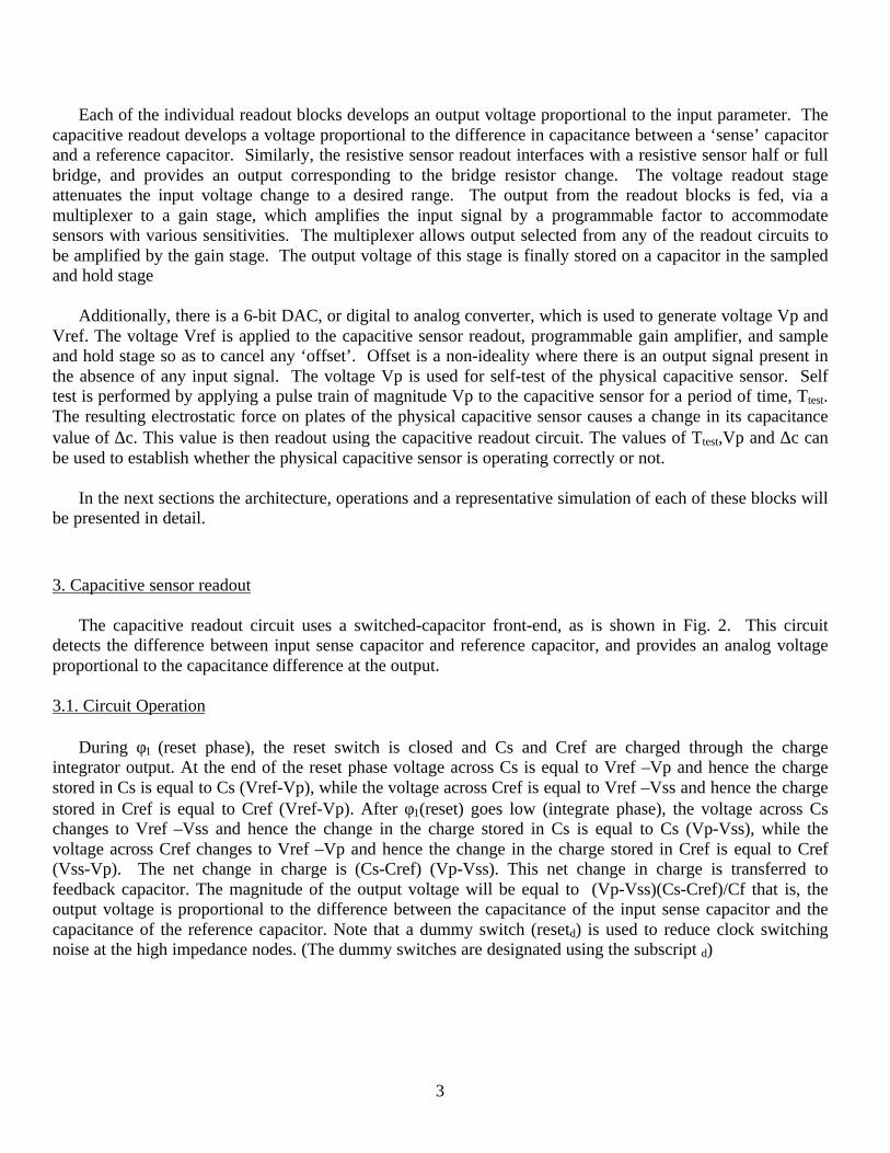
3.4. Bias circuit
The bias circuit that generates voltages Vbias1 to Vbias4 is shown separately with W/L ratios in Fig5. Thecircuit toplogy shown is known a wide swing constant transconductance bias circuit. The term wide swing isapplied since all the current mirrors are wide swing cascode current mirrors. This biasing circuit has theproperty that the transconductance of any of the transistors in the bias loop is dependent only on W/L ratiosand on the value of the resistor Rb.. The transconductance of the bias circuit determines the transconductanceof the all transistors in the OTA. This endows the OTA as a whole with immunity towards process variations.This immunity with respect to process variations was observed by running OTA simulations with all processcorners. This bias circuit is used to provide bias to all the OTAs in the switched capacitor readout circuit.
Fig. 5: Schematic of the OTA bias circuit.

7
3.5. Simulation Results
Various simulations were carried out using Star-HSPICE 2000.2. The results are tabulated below.
Table 1: Summary OTA simulated performance.
Parameter Value
Low Frequency Gain 79 dBUnity GBW 24MHzPhase Margin 46 degreesSlew Rate 49V/µsTransient Settling Time (stepsize=1v)
33ns
Power Dissipation (with bias circuit) < 1.1 mW @ 3V supplyInput/Output range 0.8 to 3VCMRR 107dB (DC)PSRR 80dBSupply voltage 3VProcess Technology 0.35um AMI, 2P, 2MLoad Capacitance 3 pF
4. Resistive sensor readout
The resistive sensor develops a voltage that varies with resistance by using a resistive full bridge, whichconverts an imbalance in resistor values to a voltage. The schematic of resistive sensor readout is shown inFig. 6.
Fig. 6: Schematic of resistive sensor readout.

8
The bridge output voltage is applied to the input of a closed loop differential amplifier. The gain of thisamplifier is given by the ratio of R2to R1 The building blocks of this circuit are the Opamp (OperationalAmplifier), and resistors.. The resistors are realized in a programmable form as shown below in Fig. 7 and Fig.8. The effective resistance is equal to the sum of resistors whose switches are open. For instance, in the casethat both switches are open the resistance value is equal to 10KΩ.
Fig. 7: Implementation of resistor R1 of Fig. 6.
Fig. 8: Implementation of resistor R2 of Fig. 6.
4.1. Opamp design
There are three main requirements on the Opamp of the resistive sensor readout front-end. A high gain isrequired to ensure precision operation, large output voltage swing is required to accommodate a large outputsignal, and the output needs to be buffered to drive current into a resistive load.
.The opamp has a two stage topology, as illustrated in Fig. 9. The first stage is an NMOS input telescopiccascode. The second stage is a PMOS common source. . MN1-MN2 form the input differential pair, MN9acts as the tail current source, MN3 MN4 are cascode transistors to the input differential pair, MP5 MP6 MP7MP8 form a wide-swing cascaded PMOS current source, MP10 is a common source amplifier and MN11 isits current source,. CC is the miller compensating capacitor and R1 is the nulling resistor.

9
Fig. 9: Schematic diagram of two stage opamp.
The gain of the Opamp is derived mainly from the first stage while the swing is produced by the secondstage. A telescopic cascode is chosen here because it dissipates about half the power of a folded cascode ofcomparable bandwidth. Miller compensation is used together with a nulling resistor so as to obtain a highphase margin with low power dissipation
4.2: Bias circuit
The bias circuit used is shown in Fig, 1A in Appendix A. The architecture is similar to the one used for theOTA, however, the sizes of the transistors used to bias the opamp nodes are different reflecting the differingbias voltage needs of the telescopic first stage.
10
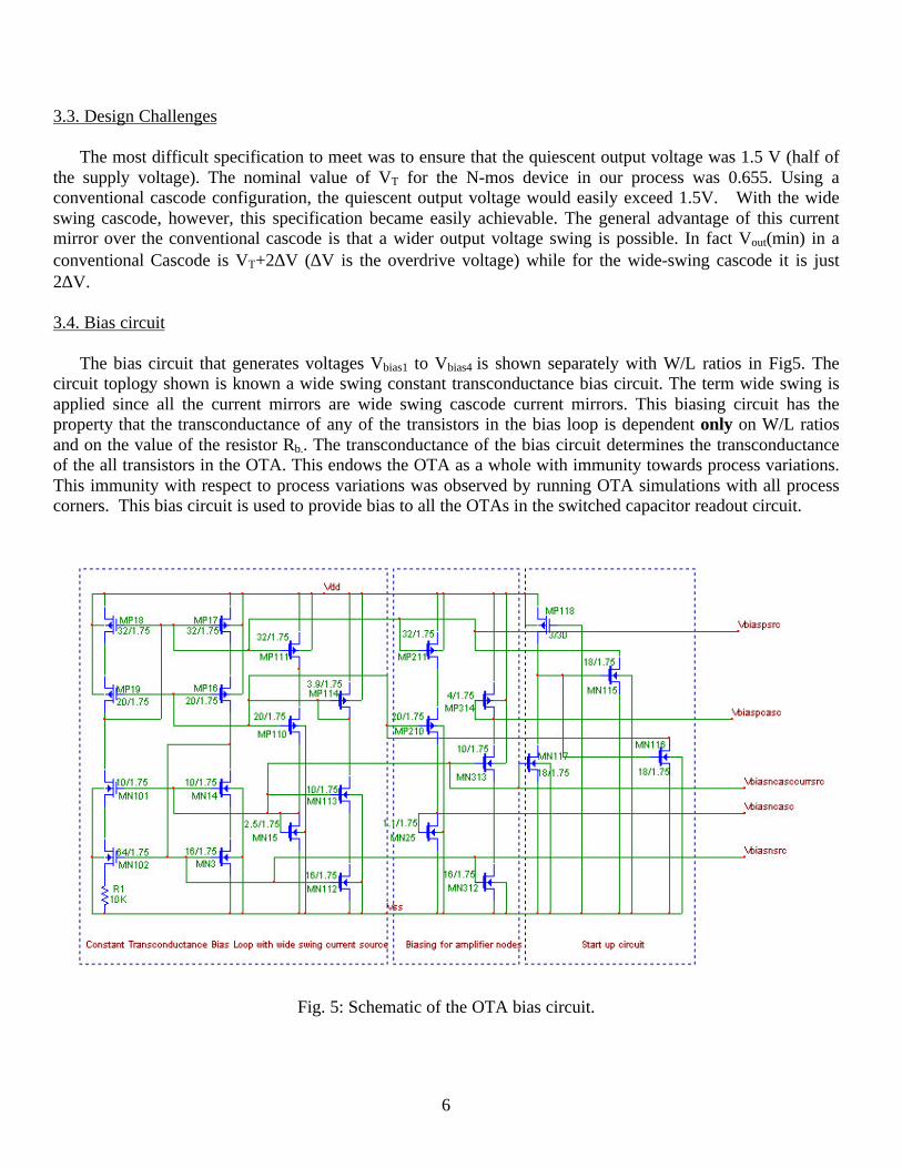
4.3: Simulation results
A summary of the simulated performance of the designed opamp is presented in Table 2.
Table 2: Summary of the opamp simulated performance.
Parameter Value
Low Frequency Gain 82 dBUnity GBW 17.6HMHzPhase Margin 86 degreesInput/Output range 0.8 to 3VCMRR 90dB (DC)Power Dissipation 2.4 mW @ 3V supplyPSRR 80dBPower supply 3VProcess Technology 0.35um AMI, 2P, 2MLoad resistor 10K
Also the resistive sensor circuit is simulated using output from a resistive full bridge so as to approximateas closely as possible operation using resistive sensor outputs. Figure 10 shows the schematic of the resistivebridge.
Fig. 10: Schematic of resistive full-bridge.
The value of delta R is swept, simulating a resistive sensor response to an input parameter. Figure 11shows the output voltage plot. and voltage of the readout circuit plotted. This plot is given on the next page.It is clearly seen that the output voltage varies non-linearly with changes in resistance

11
Fig. 11: Resistive readout output voltage versus resistance change.

12
5. Interface for sensors with voltage output
This block provides control over the voltage range, by attenuating it and feeding it to the programmablegain amplifier stage of the UMSI chip. The schematic of the voltage readout is shown in Fig. 12.
Fig. 12: Schematic diagram of the interface for sensors with voltage output.
The input voltage is attenuated by a programmable attenuator and is fed into the non inverting input of theopamp. The very high gain of the opamp forces the voltage at the inverting node (and hence the outputvoltage) to be equal to the voltage at the non inverting node. The function of the opamp is to providebuffering.
Fig. 13: Schematic of the programmable attenuator.

13
The input attenuator is implemented as shown below in Fig. 13. The programmable attenuator isimplemented as a resistive divider. The attenuation coefficient is set by the positions of the switches. Theeffective resistance of each of the legs of the resistive divider is equal to the sum of resistors whose switchesare open.
6. Programmable gain stage and sample and hold
This circuit amplifies the input voltage by a factor determined by ratio of capacitors Cin to Cf2 and holdsthis value at the output. The schematic of a programmable gain stage followed by sample and hold is shownin Fig. 14.
Fig. 14: Schematic of gain stage followed by sample and hold.
6.1. Circuit Operation:
φs (φ3) and φ2(φ4) are non overlapping clocks. During φ2 (φ3)(sample phase), the reset switch is closed andCin is charged through the charge integrator output. At the end of the reset phase voltage across Cin is equal toVin–Vref and hence the charge stored in Cin is equal to Cin (Vin-Vref). After φ3 goes high (integrate phase),the voltage across Cin changes to zero and hence the change in the charge stored in Cin is equal to Cin (Vin-Vref). This change in charge is deposited on the left plate of the feedback capacitor (a charge of equalmagnitude and opposite polarity made available through the output is deposited on the right plate of thefeedback capacitor). The magnitude of the output voltage will be equal to (Vin-Vref)(Cin)/Cf2 that is, theoutput voltage is scaled by the ratio of Cin to Cf2 . Note that a dummy switch (resetd) is used to reduce clock-switching noise at the high impedance nodes. (The dummy switches are designated using the subscript d)Whenφ3 is high φs is also high and this output voltage is sampled onto the capacitor Ch and held there until φs goeshigh again. During this time the output of the sample and hold equals the last output of the programmable gainstage.

14
The OTA, bias circuit and switches used in this circuit are same as the ones used in the capacitive readout..The input capacitor Cin and the feedback capacitor Cf2 are realized in a programmable form as shown belowin Fig. 15 and Fig. 16. The effective capacitance is the equal to the sum of the capacitors whose switches areclosed. The combination of the two programmable capacitors provides 1024 different gain settings varyingfrom 0.25 to 31.75.
Fig 15: Schematic of 7-bit programmable input capacitor array.

15
Fig. 16: 3-bit digitally programmable capacitive array connected as a feedback capacitor across the gain stage
6.2. Capacitive readout interfaced with programmable gain and sample & hold stage.
In order to illustrate one possible path through the interface circuit we have chosen the example of capacitivereadout interfaced with programmable gain and sample & hold stage.
• Fig. 17: Schematic of capacitive readout interfaced with programmable gain and sample & hold stage.

16
φ1 and φ2 are two non-overlapping clocks. During φ1, the reset switch of the charge integrator is closed andCs is charged through the charge integrator output. Once φ1 goes low, a packet of charge proportional to thedifference between Cs and Cref is integrated on the feedback capacitor. Next as φ2 goes high, the second stageis reset and, Cin charge to the output level of the first stage. The gain of the second stage is determined by theratio of the total capacitance switched into its input to the feedback capacitance Cf2. Clock phases φ3 and φ4
are slightly delayed φ1 and φ2 clock phases Finally, the output of the second stage is sampled and held at theinput of the third stage during φs.
6.3. Simulation Results
The circuit was simulated using the capacitors values shown in Table 3. Vref is taken to be 1.5v Vp is takento be 3 V, Vss =0V. The clocks had a frequency of 2/3 MHz. The non-overlap time of the clock phases was250 ns. The clock delays are 100 ns. The simulation output waveform is presented in Fig. 18.
Table 3: The capacitor values used in the capacitive readout, programmablegain amplifier, and sample & hold simulations.
Capacitor ValueCs1 3.2pF
Cref1 3pFCf1 3pFCin 9pFCf2 3pFCh 3pF
This graph shows the clock phase φs (dotted line) well as the output voltage (solid line). The result showsthat for an input capacitance difference of 0.2pF the output voltage changes by 0.6V.This predicted byequation ∆Vout =(∆C/Cref)*(Cin/Cf2)*(Vp-Vss).

17
Fig. 18: Simulated output of the capacitive readout, programmable gain amplifier, and sample & hold stage.
18
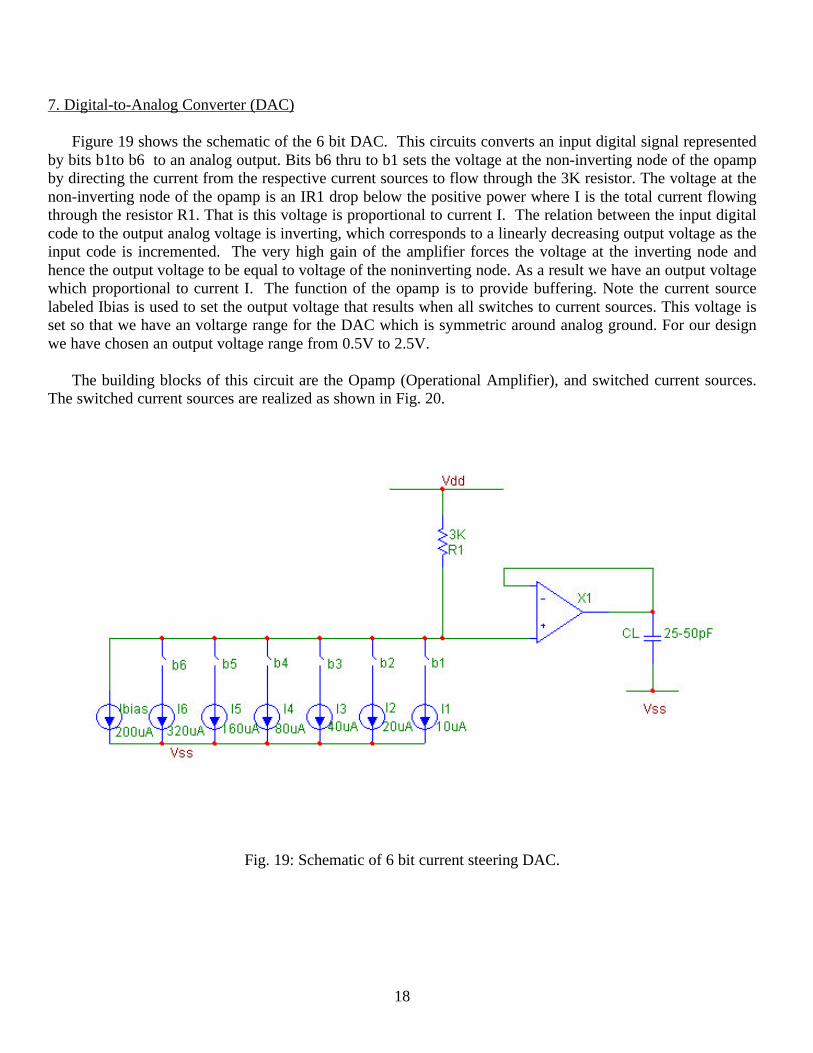
7. Digital-to-Analog Converter (DAC)
Figure 19 shows the schematic of the 6 bit DAC. This circuits converts an input digital signal representedby bits b1to b6 to an analog output. Bits b6 thru to b1 sets the voltage at the non-inverting node of the opampby directing the current from the respective current sources to flow through the 3K resistor. The voltage at thenon-inverting node of the opamp is an IR1 drop below the positive power where I is the total current flowingthrough the resistor R1. That is this voltage is proportional to current I. The relation between the input digitalcode to the output analog voltage is inverting, which corresponds to a linearly decreasing output voltage as theinput code is incremented. The very high gain of the amplifier forces the voltage at the inverting node andhence the output voltage to be equal to voltage of the noninverting node. As a result we have an output voltagewhich proportional to current I. The function of the opamp is to provide buffering. Note the current sourcelabeled Ibias is used to set the output voltage that results when all switches to current sources. This voltage isset so that we have an voltarge range for the DAC which is symmetric around analog ground. For our designwe have chosen an output voltage range from 0.5V to 2.5V.
The building blocks of this circuit are the Opamp (Operational Amplifier), and switched current sources.The switched current sources are realized as shown in Fig. 20.
Fig. 19: Schematic of 6 bit current steering DAC.
19
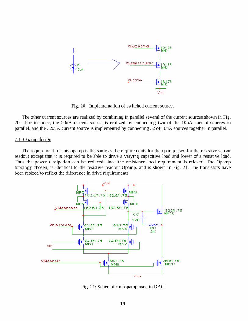
Fig. 20: Implementation of switched current source.
The other current sources are realized by combining in parallel several of the current sources shown in Fig.20. For instance, the 20uA current source is realized by connecting two of the 10uA current sources inparallel, and the 320uA current source is implemented by connecting 32 of 10uA sources together in parallel.
7.1. Opamp design
The requirement for this opamp is the same as the requirements for the opamp used for the resistive sensorreadout except that it is required to be able to drive a varying capacitive load and lower of a resistive load.Thus the power dissipation can be reduced since the resistance load requirement is relaxed. The Opamptopology chosen, is identical to the resistive readout Opamp, and is shown in Fig. 21. The transistors havebeen resized to reflect the difference in drive requirements.
Fig. 21: Schematic of opamp used in DAC

20
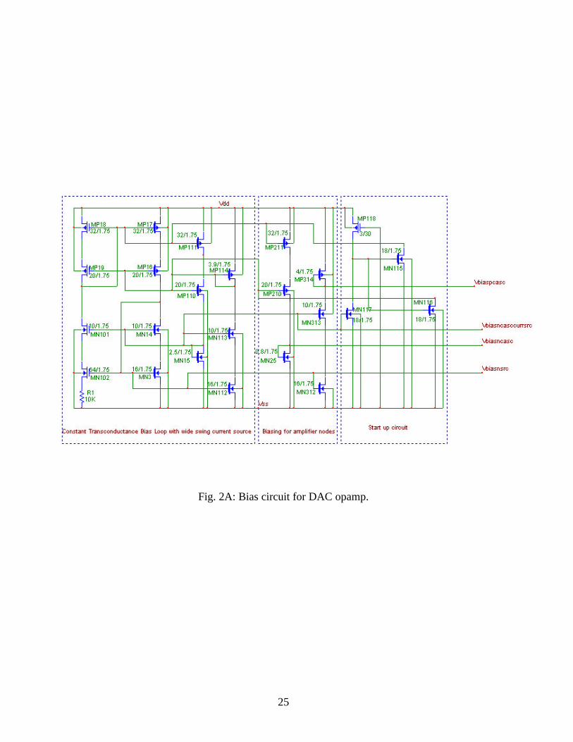
7.2. Bias circuit
The bias circuit used is shown in Fig. 2A of Appendix A. The architecture is similar to the previouslypresented bias circuits in this report, however, the sizes of the transistors used to bias the opamp nodes arechanged to reflect the different bias voltage needs of this opamp.
7.3. Simulation results
The simulated performance of the DAC opamp is presented in Table 3. The load capacitances in thesimulations were deliberately chosen to be large values. The reason for this choice is that the phase margin fortwo stage amplifiers decrease with increasing load capacitance. So if we verify that the amplifier has a highphase margin for a 50 pF load capacitance, the stability for smaller capacitive is verified as well. Also notethe amplifier has a large dc gain, which provides better than 11b accurate unity gain buffer for input voltagerange from 0.5V to 2.5V.
Table 3: Summary of the DAC opamp simulated performance.
Parameter Value
Low Frequency Gain 120 dBUnity GBW 6 MHz with load
capacitance = 25 pF5 Mhz with loadcapacitance = 50 pF
Load Capacitance 25-50pFPhase Margin 89 degrees with load
capacitance = 25 pF73.8 degrees with loadcapacitance = 50 pF
Input/Output range 0.8 to 3VCMRR 90dB (DC)Power Dissipation 780uW @ 3V supplyPSRR 80dBPower supply 3VProcess Technology 0.35um AMI, 2P, 2M
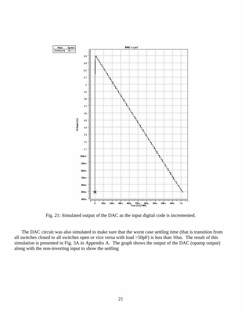
The DAC was simulated, stepping the bits controlling the switched current sources from 000000 all theway up to 111111 one bit at a time. The simulation waveform is presented in Fig. 21. The output has adescending staircase shape that corresponds to the inverting relation between the input digital code to theoutput analog voltage. The output steps down uniformly in response to uniform periodic increments in inputall the way from 2.5V to 0.5V
21
Fig. 21: Simulated output of the DAC as the input digital code is incremented.
The DAC circuit was also simulated to make sure that the worst case settling time (that is transition fromall switches closed to all switches open or vice versa with load =50pF) is less than 10us. The result of thissimulation is presented in Fig. 3A in Appendix A. The graph shows the output of the DAC (opamp output)along with the non-inverting input to show the settling

22
Analog ground (Vref) generation.
The buffer used for the DAC can also be used to generate the Vref analog ground signal. The voltagebetween the positive power supply and ground is divided by two. The divider is formed by two the resistiveR1 and R2 as is shown in Fig. 21. This voltage is applied to the non-inverting terminal of the opamp. The veryhigh gain of the opamp forces the voltage at the inverting node (and hence the output voltage) to be equal tothe voltage at the non-inverting node. The function of the opamp is to buffer the voltage.
Fig. 22: Schematic of Vref (Analog ground) generator.

23
Appendix A

24
Fig. 1A: Bias circuit for resistive readout opamp.
25
Fig. 2A: Bias circuit for DAC opamp.

26
Fig3A: Worst case settling time for DAC.