an74 - component and measurement advances ensure 16-bit
TRANSCRIPT

Application Note 74
AN74-1
Component and Measurement Advances Ensure16-Bit DAC Settling TimeThe art of timely accuracy
Jim Williams
July 1998
Introduction
Instrumentation, waveform generation, data acquisition,feedback control systems and other application areas arebeginning to utilize 16-bit data converters. More specifi-cally, 16-bit digital-to-analog converters (DACs) haveseen increasing use. New components (see Componentsfor 16-Bit Digital-to-Analog Conversion, page 2) havemade 16-bit DACs a practical design alternative1. TheseICs provide 16-bit performance at reasonable cost com-pared to previous modular and hybrid technologies. TheDC and AC specifications of the monolithic DAC’sapproach or equal previous converters at significantlylower cost.
DAC Settling Time
DAC DC specifications are relatively easy to verify. Mea-surement techniques are well understood, albeit oftentedious. AC specifications require more sophisticatedapproaches to produce reliable information. In particular,the settling time of the DAC and its output amplifier isextraordinarily difficult to determine to 16-bit resolution.DAC settling time is the elapsed time from input codeapplication until the output arrives at and remains withina specified error band around the final value. It is usuallyspecified for a full-scale 10V transition. Figure 1 showsthat DAC settling time has three distinct components. Thedelay time is very small and is almost entirely due topropagation delay through the DAC and output amplifier.During this interval there is no output movement. Duringslew time the output amplifier moves at its highest pos-sible speed towards the final value. Ring time defines theregion where the amplifier recovers from slewing and
DAC INPUT (ALL BITS)
DAC OUTPUT
AN74 F01
SETTLING TIME
SLEW TIME
RING TIME
ALLOWABLE OUTPUT ERROR BAND
DELAY TIME
Note 1. See Appendix A, “A History of High Accuracy Digital-to-AnalogConversion”.Note 2. This issue is treated in detail in latter portions of the text. Alsosee Appendix D “Practical Considerations for DAC-AmplifierCompensation.
, LTC and LT are registered trademarks of Linear Technology Corporation.
ceases movement within some defined error band. Thereis normally a trade-off between slew and ring time. Fastslewing amplifiers generally have extended ring times,complicating amplifier choice and frequency compensa-tion. Additionally, the architecture of very fast amplifiersusually dictates trade-offs which degrade DC error terms.2
Measuring anything at any speed to 16 bits (≈0.0015%)is hard. Dynamic measurement to 16-bit resolution isparticularly challenging. Reliable 16-bit settling timemeasurement constitutes a high order difficulty problemrequiring exceptional care in approach and experimentaltechnique.
Figure 1. DAC Settling Time Components Include Delay, Slewand Ring Times. Fast Amplifiers Reduce Slew Time, AlthoughLonger Ring Time Usually Results. Delay Time is Normally aSmall Term

Application Note 74
AN74-2
COMPONENTS FOR 16-BIT D/A CONVERSION
Components suitable for 16-bit D/A conversion aremembers of an elite class. 16 binary bits is one part in65,536—just 0.0015% or 15 parts-per-million. Thismandates a vanishingly small error budget and thedemands on components are high. The digital-to-ana-log converters listed in the chart all use Si-Chrome thin-film resistors for high stability and linearity over
temperature. Gain drift is typically 1ppm/°C or about2LSBs over 0°C to 70°C. The amplifiers shown contrib-ute less than 1LSB error over 0°C to 70°C with 16-bitDAC driven settling times of 1.7µs available. The refer-ences offer drifts as low as 1LSB over 0°C to 70°C withinitial trimmed accuracy to 0.05%
Short Form Descriptions of Components Suitable for 16-Bit Digital-to-Analog ConversionCOMPONENT TYPE ERROR CONTRIBUTION OVER 0°C TO 70°C COMMENTS
LTC®1597 DAC ≈2LSB Gain Drift Full Parallel Inputs 1LSB Linearity Current Output
LTC1595 DAC ≈2LSB Gain Drift Serial Input 1LSB Linearity 8-PIn Package
Current Output
LTC1650 DAC ≈3.5LSB Gain Drift Complete Voltage 6LSB Offset Output DAC 4LSB Linearity
LT®1001 Amplifier <1LSB Good Low Speed Choice10mA Output Capability
LT1012 Amplifier <1LSB Good Low Speed ChoiceLow Power Consumption
LT1468 Amplifier <2LSB 1.7µs Settling to 16 BitsFastest Available
LM199A Reference-6.95V ≈1LSB Lowest Drift Referencein This Group
LT1021 Reference-10V ≈4LSB Good General Purpose Choice
LT1027 Reference-5V ≈4LSB Good General Purpose Choice
LT1236 Reference-10V ≈10LSB Trimmed to 0.05% AbsoluteAccuracy
LT1461 Reference-4.096V ≈10LSB Recommended for LTC1650DACs (see Above)
Considerations for Measuring DAC Settling Time
Historically, DAC settling time has been measured withcircuits similar to that in Figure 2. The circuit uses the“false sum node” technique. The resistors and DAC-amplifier form a bridge type network. Assuming idealresistors, the amplifier output will step to VIN when theDAC inputs move to all ones. During slew, the settle nodeis bounded by the diodes, limiting voltage excursion.When settling occurs, the oscilloscope probe voltage
should be zero. Note that the resistor divider’s attenuationmeans the probe’s output will be one-half of the actualsettled voltage.
In theory, this circuit allows settling to be observed tosmall amplitudes. In practice, it cannot be relied upon toproduce useful measurements. The oscilloscope connec-tion presents problems. As probe capacitance rises, ACloading of the resistor junction influences observed set-tling waveforms. A 10pF probe alleviates this problem but

Application Note 74
AN74-3
DIGITAL INPUTS
REF
FB
DAC
0V TO 10V TRANSITION
SETTLE NODE
INPUT FROM
PULSE GENERATOR
R
AN74 F02
R
INPUT STEP TO OSCILLOSCOPE
OUTPUT TO OSCILLOSCOPE
OUTPUT AMPLIFIER
DIGITAL INPUTS
–VREF
–
+
Figure 2. Popular Summing Scheme for DAC Settling Time Measurement Provides Misleading Results.16-Bit Measurement Causes >200 × Oscilloscope Overdrive. Displayed Information is Meaningless
its 10× attenuation sacrifices oscilloscope gain.1× probes are not suitable because of their excessive inputcapacitance. An active 1× FET probe will work, but anotherissue remains.
The clamp diodes at the settle node are intended to reduceswing during amplifier slewing, preventing excessive os-cilloscope overdrive. Unfortunately, oscilloscope overdriverecovery characteristics vary widely among different typesand are not usually specified. The Schottky diodes’ 400mVdrop means the oscilloscope may see an unacceptableoverload, bringing displayed results into question.3
At 10-bit resolution (10mV at the DAC output—5mV at theoscilloscope), the oscilloscope typically undergoes a 2×overdrive at 50mV/DIV, and the desired 5mV baseline isjust discernible. At 12-bit or higher resolution, the mea-surement becomes hopeless with this arrangement. In-creasing oscilloscope gain brings commensurate increasedvulnerability to overdrive induced errors. At 16 bits, thereis clearly no chance of measurement integrity.
The preceding discussion indicates that measuring 16-bitsettling time requires a high gain oscilloscope that issomehow immune to overdrive. The gain issue is addres-sable with an external wideband preamplifier that accu-rately amplifies the diode-clamped settle node. Gettingaround the overdrive problem is more difficult.
The only oscilloscope technology that offers inherentoverdrive immunity is the classical sampling ‘scope.4Unfortunately, these instruments are no longer manufac-
tured (although still available on the secondary market).It is possible, however, to construct a circuit that borrowsthe overload advantages of classical sampling ‘scopetechnology. Additionally, the circuit can be endowed withfeatures particularly suited for measuring 16-bit DACsettling time.
Practical DAC Settling Time Measurement
Figure 3 is a conceptual diagram of a 16-bit DAC settling-time-measurement circuit. This figure shares attributeswith Figure 2, although some new features appear. In thiscase, the preamplified oscilloscope is connected to thesettle point by a switch. The switch state is determined bya delayed pulse generator, which is triggered from thesame pulse that controls the DAC. The delayed pulsegenerator’s timing is arranged so that the switch does notclose until settling is very nearly complete. In this way theincoming waveform is sampled in time, as well as ampli-tude. The oscilloscope is never subjected to overdrive—no off-screen activity ever occurs.
Note 3: For a discussion of oscilloscope overdrive considerations, seeAppendix B, “Evaluating Oscilloscope Overdrive Performance”.Note 4: Classical sampling oscilloscopes should not be confused withmodern era digital sampling ‘scopes that have overdrive restrictions.See Appendix B, “Evaluating Oscilloscope Overload Performance” forcomparisons of various type ‘scopes with respect to overdrive. Fordetailed discussion of classical sampling ‘scope operation seereferences 14 through 17 and 20 through 22. Reference 15 isnoteworthy; it is the most clearly written, concise explanation ofclassical sampling instruments the author is aware of. A 12 page jewel.

Application Note 74
AN74-4
DIGITAL INPUTS
REF
FB
DAC0V TO 10V TRANSITION
SETTLE NODE
INPUT FROM
PULSE GENERATOR
R
AN74 F04
R
TIME CORRECTED INPUT STEP TO OSCILLOSCOPE
OUTPUT TO OSCILLOSCOPE 0.01V/DIV = 500µV/DIV AT DAC AMPLIFIER OUTPUT
OUTPUT AMPLIFIER
SAMPLING BRIDGE DRIVER
SAMPLING BRIDGE SWITCH
DIGITAL INPUTS
–VREF
–
+ RESIDUE AMPLIFIER
BRIDGE SWITCHING CONTROL
VARIABLE DELAY
DELAYED PULSE GENERATOR
BRIDGE DRIVER/RESIDUE AMPLIFIER DELAY COMPENSATION
VARIABLE WIDTH PULSE GENERATOR
SAMPLING BRIDGE TEMPERATURE
CONTROL
×40×1
DIGITAL INPUTS
REF
FB
DAC
SETTLE NODE SWITCH
INPUT FROM
PULSE GENERATOR
R
AN74 F03
R
INPUT STEP TO OSCILLOSCOPE
OUTPUT TO OSCILLOSCOPE
OUTPUT AMPLIFIER
PREAMPLIFIER
DIGITAL INPUTS
–VREF
–
+
DELAYED PULSE GENERATOR
Figure 4. Block Diagram of DAC Settling Time Measurement Scheme. Diode Bridge Switch Minimizes Switching Feedthrough,Preventing Residue Amplifier-Oscilloscope Overdrive. Temperature Control Maintains 10µV Switch Offset Baseline. Input StepTime Reference is Compensated for ×1 and ×40 Amplifier Delays
Figure 4 is a more complete representation of the DACsettling time scheme. Figure 3’s blocks appear in greaterdetail and some new refinements show up. The DAC-amplifier summing area is unchanged. Figure 3’s delayedpulse generator has been split into two blocks; a delay anda pulse generator, both independently variable. The inputstep to the oscilloscope runs through a section that
compensates for the propagation delay of the settling-time-measurement path. The most striking new aspect ofthe diagram is the diode bridge switch. Borrowed fromclassical sampling oscilloscope circuitry, it is the key tothe measurement. The diode bridge’s inherent balanceeliminates charge injection based errors in the output. Itis far superior to other electronic switches in this
Figure 3. Conceptual Arrangement Eliminates Oscilloscope Overdrive. Delayed Pulse Generator ControlsSwitch, Preventing Oscilloscope from Monitoring Settle Node Until Settling is Nearly Complete
Application Note 74
AN74-5
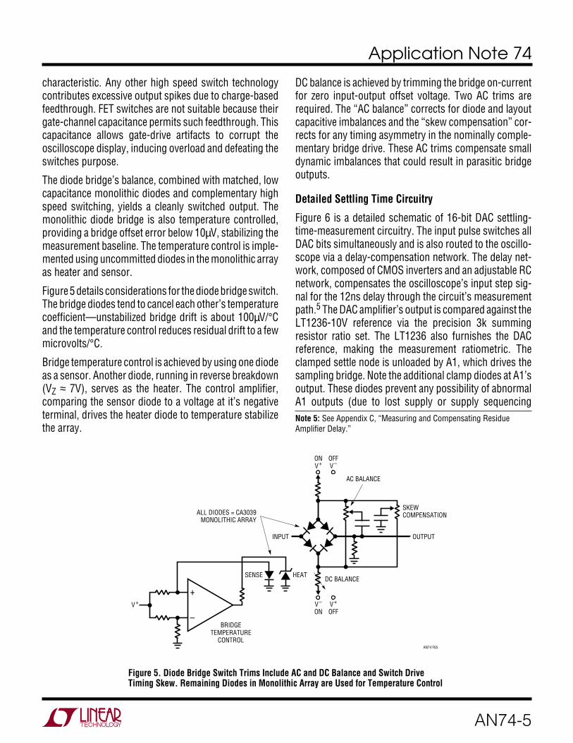
characteristic. Any other high speed switch technologycontributes excessive output spikes due to charge-basedfeedthrough. FET switches are not suitable because theirgate-channel capacitance permits such feedthrough. Thiscapacitance allows gate-drive artifacts to corrupt theoscilloscope display, inducing overload and defeating theswitches purpose.
The diode bridge’s balance, combined with matched, lowcapacitance monolithic diodes and complementary highspeed switching, yields a cleanly switched output. Themonolithic diode bridge is also temperature controlled,providing a bridge offset error below 10µV, stabilizing themeasurement baseline. The temperature control is imple-mented using uncommitted diodes in the monolithic arrayas heater and sensor.
Figure 5 details considerations for the diode bridge switch.The bridge diodes tend to cancel each other’s temperaturecoefficient—unstabilized bridge drift is about 100µV/°Cand the temperature control reduces residual drift to a fewmicrovolts/°C.
Bridge temperature control is achieved by using one diodeas a sensor. Another diode, running in reverse breakdown(VZ ≈ 7V), serves as the heater. The control amplifier,comparing the sensor diode to a voltage at it’s negativeterminal, drives the heater diode to temperature stabilizethe array.
Figure 5. Diode Bridge Switch Trims Include AC and DC Balance and Switch DriveTiming Skew. Remaining Diodes in Monolithic Array are Used for Temperature Control
DC balance is achieved by trimming the bridge on-currentfor zero input-output offset voltage. Two AC trims arerequired. The “AC balance” corrects for diode and layoutcapacitive imbalances and the “skew compensation” cor-rects for any timing asymmetry in the nominally comple-mentary bridge drive. These AC trims compensate smalldynamic imbalances that could result in parasitic bridgeoutputs.
Detailed Settling Time Circuitry
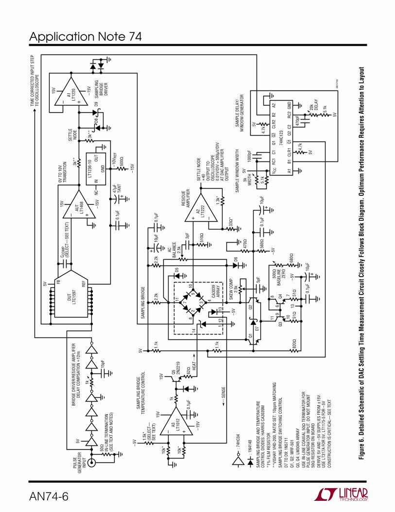
Figure 6 is a detailed schematic of 16-bit DAC settling-time-measurement circuitry. The input pulse switches allDAC bits simultaneously and is also routed to the oscillo-scope via a delay-compensation network. The delay net-work, composed of CMOS inverters and an adjustable RCnetwork, compensates the oscilloscope’s input step sig-nal for the 12ns delay through the circuit’s measurementpath.5 The DAC amplifier’s output is compared against theLT1236-10V reference via the precision 3k summingresistor ratio set. The LT1236 also furnishes the DACreference, making the measurement ratiometric. Theclamped settle node is unloaded by A1, which drives thesampling bridge. Note the additional clamp diodes at A1’soutput. These diodes prevent any possibility of abnormalA1 outputs (due to lost supply or supply sequencingNote 5: See Appendix C, “Measuring and Compensating ResidueAmplifier Delay.”
ON V+
OFF V–
V– ON
V+
OFF
SKEW COMPENSATION
OUTPUT
AC BALANCE
DC BALANCE
AN74 F05
INPUT
SENSE
BRIDGE TEMPERATURE
CONTROL
HEAT
–
+V+
ALL DIODES = CA3039 MONOLITHIC ARRAY
Application Note 74
AN74-6
+
711D5
AC
BALA
NCE
2.5k
RESI
DUE
AMPL
IFIE
R
SETT
LE N
ODE
×40
OU
TPUT
TO
OSCI
LLOS
COPE
0.
01V/
DIV
= 50
0µV/
DIV
AT D
AC A
MPL
IFIE
R OU
TPUT
SAM
PLIN
G BR
IDGE
SAM
PLIN
G BR
IDGE
TE
MPE
RATU
RE C
ONTR
OL
108
4
14
1.1k
Q1
Q4
11 1013
8 7
96
Q3
5pF
3pF
0.1µ
F10
µF
510Ω
D633
Ω*
1.3k
*
Q2
D7
CA30
39
ARRA
Y12
113
–5V
–5V
–5V
SKEW
COM
P 2.
5k
3
25
2.2k
1.1k
5V
15V
15V
–15V
–5V
1k
0.1µ
F
2.2k
10µF
0.1µ
F
470Ω
560Ω
51Ω
820Ω
51Ω
680Ω
500Ω
BA
SELI
NE
ZERO
62Ω HE
AT
SENS
E
: 74H
C04
: 1N4
148
SAM
PLIN
G BR
IDGE
AND
TEM
PERA
TURE
CO
NTRO
L DI
ODES
: HAR
RIS
CA30
39M
*1
% F
ILM
RES
ISTO
R **
VISH
AY V
HD-2
00, R
ATIO
SET
: 10p
pm M
ATCH
ING
SAM
PLIN
G BR
IDGE
SW
ITCH
ING
CONT
ROL
D7 T
O D9
: 1N5
711
Q1, Q
2: M
RF-5
01
Q3, Q
4: L
M30
45 A
RRAY
US
E IN
-LIN
E CO
AXIA
L 50
Ω T
ERM
INAT
OR F
OR
PULS
E GE
NERA
TOR
INPU
T. D
O NO
T M
OUNT
50
Ω R
ESIS
TOR
ON B
OARD
DE
RIVE
5V
AND
–5V
SUPP
LIES
FRO
M ±
15V.
US
E LT
317A
FOR
5V,
LT1
175-
5 FO
R –5
V CO
NSTR
UCTI
ON IS
CRI
TICA
L—SE
E TE
XT
Q5
2N22
19
1.5k
* (S
ELEC
T—
SEE
TEXT
)
10k*
10k*
–+A2
LT
1222
– +
A3
LT10
12
0.1µ
F10
µF
+
+
V CC
RC1
5k
WID
TH5V
SAM
PLE
WIN
DOW
WID
THSA
MPL
E DE
LAY/
W
INDO
W G
ENER
ATOR
5V
5V
74HC
123
5V
4.7k
4.7k
20k
DELA
Y
1000
pF
5.1k
C1Q1
Q2CL
R2B2
A2
A1B1
CLR1
Q1Q2
C2RC
2GN
D
470p
F
AN74
F06
5.1k
REFFB5V
15V
LT12
36-1
0 OUT
NCIN
47µF
TA
NT0.
1µF
500Ω
–10V
REF
GND
SAM
PLIN
G BR
IDGE
DR
IVER
SETT
LE
NODE
3k**
–15V
15V
–15V
–15V
DUT
LTC1
597
C COM
P (S
ELEC
T—SE
E TE
XT)
0V T
O 10
V TR
ANSI
TION
TIM
E CO
RREC
TED
INPU
T ST
EP
TO O
SCIL
LOSC
OPE
– +
15pF
1k
5VPU
LSE
GENE
RATO
R IN
PUT
50Ω
IN
-LIN
E TE
RMIN
ATIO
N (S
EE T
EXT
AND
NOTE
S)
BRID
GE D
RIVE
R/RE
SIDU
E AM
PLIF
IER
DELA
Y CO
MPS
ATIO
N ≈
12ns
AUT
LT14
68
+
3k**
D8D9
– +
A1
LT12
20
Figu
re 6
. Det
aile
d Sc
hem
atic
of D
AC S
ettli
ng T
ime
Mea
sure
men
t Circ
uit C
lose
ly F
ollo
ws
Bloc
k Di
agra
m. O
ptim
um P
erfo
rman
ce R
equi
res
Atte
ntio
n to
Lay
out

Application Note 74
AN74-7
anomalies) from damaging the diode array.6 A3 andassociated components temperature control the sam-pling diode bridge by comparing a diodes’s forward dropto a stable potential derived from the – 5V regulator.Another diode, operated in the reverse direction (VZ ≈ 7V)serves as a chip heater. The pin connections shown onthe schematic have been selected to provide best tem-perature control performance.
The input pulse triggers the 74HC123 one shot. The oneshot is arranged to produce a delayed (controllable by the20k potentiometer) pulse whose width (controllable by the5k potentiometer) sets diode bridge on-time. If the delayis set appropriately, the oscilloscope will not see any inputuntil settling is nearly complete, eliminating overdrive. Thesample window width is adjusted so that all remainingsettling activity is observable. In this way the oscilloscope’soutput is reliable and meaningful data may be taken. Theone shot’s output is level shifted by the Q1-Q4 transistors,providing complementary switching drive to the bridge.The actual switching transistors, Q1-Q2, are UHF types,permitting true differential bridge switching with less than1ns of time skew.7
A2 monitors the bridge output, provides gain and drivesthe oscilloscope. Figure 7 shows circuit waveforms. TraceA is the input pulse, trace B the DAC amplifier output, traceC the sample gate and trace D the residue amplifier output.When the sample gate goes low, the bridge switchescleanly, and the last 1.5mV of slew are easily observed.Ring time is also clearly visible, and the amplifier settlesnicely to final value. When the sample gate goes high, thebridge switches off, with only 600µV of feedthrough. The
100µV peak before bridge switching (at ≈3.5 verticaldivisions) is feedthrough from A1’s output, but it issimilarly well controlled. Note that there is no off-screenactivity at any time—the oscilloscope is never subjectedto overdrive.
The circuit requires trimming to achieve this level ofperformance. The bridge temperature control point is setby grounding Q5’s base prior to applying power. Next,apply power and measure A3’s positive input with respectto the –5V rail. Select the indicated resistor (1.5k nominal)for a voltage at A3’s negative input (again, with respect to–5V) that is 57mV below the positive input’s value.Unground Q5’s base and the circuit will control the sam-pling bridge to about 55°C:
25°C room + 57
1 9mV
mV C diode drop. / °= 30°C rise = 55°C
The DC and AC bridge trims are made once the tempera-ture control is functional. Making these adjustmentsrequires disabling the DAC and amplifier (disconnect theinput pulse from the DAC and set all DAC inputs low) andshorting the settle node directly to the ground plane.Figure 8 shows typical results before trimming. Trace A isthe input pulse, trace B the sample gate and trace C theresidue amplifier output. With the DAC-amplifier disabled
A = 10V/DIV
B = 10V/DIV
C = 10V/DIV
D = 500µV/DIV
1µs/DIVAN74 F07
Figure 7. Settling Time Circuit Waveforms Include TimeCorrected Input Pulse (Trace A), DAC Amplifier Output (Trace B),Sample Gate (Trace C) and Settling Time Output (Trace D).Sample Gate Window’s Delay and Width are Variable
Note 6: This can and did happen. The author was unfit for humancompanionship upon discovering this mishap. Replacing the samplingbridge was a lengthy and highly emotionally charged task. To see why,refer to Appendix G, “Breadboarding, Layout and ConnectionTechniques.”Note 7: The bridge switching scheme was developed at LTC byGeorge Feliz.
1µs/DIVAN74 F08
B = 10V/DIV
A = 10V/DIV
C = 500µV/DIV
Figure 8. Settling Time Circuit’s Output (Trace C) withUnadjusted Sampling Bridge AC and DC Trims. DAC is Disabledand Settle Node Grounded for This Test. Excessive Switch DriveFeedthrough and Baseline Offset are Present. Traces A and Bare Input Pulse and Sample Window, Respectively

Application Note 74
AN74-8
and the settle node grounded, the residue amplifier outputshould (theoretically) always be zero. The photo showsthis is not the case for an untrimmed bridge. AC and DCerrors are present. The sample gate’s transitions causelarge, off-screen residue amplifier swings (note residueamplifier’s response to the sample gate’s turn-off at the≈8.5 vertical division). Additionally, the residue amplifieroutput shows significant DC offset error during the sam-pling interval. Adjusting the AC balance and skew compen-sation minimizes the switching induced transients. TheDC offset is adjusted out with the baseline zero trim. Figure9 shows the results after making these adjustments. Allswitching related activity is now well on-screen and offseterror reduced to unreadable levels. Once this level ofperformance has been achieved, the circuit is ready foruse.8 Unground the settle node and restore the input pulseconnection to the DAC.
Note 8: Achieving this level of performance also depends on layout.The circuit’s construction involves a number of subtleties and isabsolutely crucial. Please see Appendix G, “Breadboarding, Layout andConnection Techniques.”
1µs/DIVAN74 F12
A = 10V/DIV
B = 500µV/DIV
Figure 12. Optimal Sample Gate Delay Positions SamplingWindow (Trace A) So All Settle Output (Trace B) Informationis Well Inside Screen Boundaries
In general, it is good practice to “walk” the samplingwindow up to the last millivolt or so of amplifier slewing sothat the onset of ring time is observable. The samplingbased approach provides this capability and it is a verypowerful measurement tool. Additionally, remember that
B = 500µV/DIV
1µs/DIVAN74 F10
A = 10V/DIV
Figure 10. Oscilloscope Display with Inadequate Sample GateDelay. Sample Window (Trace A) Occurs Too Early, Resulting inOff-Screen Activity in Settle Output (Trace B). Oscilloscope isOverdriven, Making Displayed Information Questionable
1µs/DIVAN74 F09
B = 10V/DIVA = 10V/DIV
C = 500µV/DIV
Figure 9. Settling Time Circuit’s Output (Trace C) with SamplingBridge Trimmed. As in Figure 8, DAC is Disabled and SettleNode Grounded for This Test. Switch Drive Feedthrough andBaseline Offset are Minimized. Traces A and B are Input Pulseand Sampling Gate, Respectively
Using the Sampling-Based Settling Time Circuit
Figures 10 through 12 underscore the importance ofpositioning the sampling window properly in time. InFigure 10 the sample gate delay initiates the samplewindow (trace A) too early and the residue amplifier’soutput (trace B) overdrives the oscilloscope when sam-pling commences. Figure 11 is better, with only slight off-screen activity. Figure 12 is optimal. All amplifier residueis well inside the screen boundaries.
1µs/DIVAN74 F11
A = 10V/DIV
B = 500µV/DIV
Figure 11. Increasing Sample Gate Delay PositionsSample Window (Trace A) So Settle Output (Trace B)Activity is On-Screen

Application Note 74
AN74-9
slower amplifiers may require extended delay and/or sam-pling window times. This may necessitate larger capacitorvalues in the 74H123 one-shot timing networks.
Compensation Capacitor Effects
The DAC amplifier requires frequency compensation toget the best possible settling time. The DAC has appre-ciable output capacitance, complicating amplifier responseand making careful compensation capacitor selectioneven more important.9 Figure 13 shows effects of verylight compensation. Trace A is the time corrected inputpulse and trace B the residue amplifier output. The lightcompensation permits very fast slewing but excessiveringing amplitude over a protracted time results. Theringing is so severe that it feeds through during a portionof the sample gate off-period, although no overdriveresults. When sampling is initiated (just prior to the sixthvertical division) the ringing is seen to be in its final stages,although still offensive. Total settling time is about 2.8µs.Figure 14 presents the opposite extreme. Here a largevalue compensation capacitor eliminates all ringing butslows down the amplifier so much that settling stretchesout to 3.3µs. The best case appears in Figure 15. Thisphoto was taken with the compensation capacitor care-fully chosen for the best possible settling time. Dampingis tightly controlled and settling time goes down to 1.7µs.
500ns/DIVAN74 F14
A = 5V/DIV
B = 500µV/DIV
500ns/DIVAN74 F15
B = 500µV/DIV
A = 5V/DIV
Verifying Results—Alternate Methods
The sampling-based settling time circuit appears to be auseful measurement solution. How can its results betested to ensure confidence? A good way is to make thesame measurement with alternate methods and see ifresults agree. To begin this exercise we return to the basicdiode-bounded settle circuit.
Figure 16 repeats Figure 2’s basic settling time measure-ment, with the same problem. The Schottky-boundedsettle node forces a 400mV overdrive to the oscilloscope,
TO OSCILLOSCOPE
AN74 F16
SETTLE NODE
POSITIVE OUTPUT FROM DAC AMPLIFIER
–VREF
R
R
Figure 14. Excessive Feedback CapacitanceOverdamps Response. tSETTLE = 3.3µs
Figure 15. Optimal Feedback Capacitance Yields TightlyDamped Signature and Best Settling Time. tSETTLE = 1.7µs
Figure 16. Clamped Settle Node Permits OscilloscopeOverdrive Because Diodes Have 400mV Drop
Note 9: This section discusses frequency compensation of the DACamplifier within the context of sampling-based settling time measure-ment. As such, it is necessarily brief. Considerably more detail isavailable later in the text and in Appendix D, “Practical Considerationsfor DAC-Amplifier Compensation.”
500ns/DIVAN74 F13
A = 5V/DIV
B = 500µV/DIV
Figure 13. Settling Profile with Inadequate FeedbackCapacitance Shows Underdamped Response. Excessive RingingFeeds Through During Sample Gate Off-Period (Second Through≈Sixth Vertical Divisions) But is Tolerable. tSETTLE = 2.8µs

Application Note 74
AN74-10
rendering all measurements useless. Now, consider Fig-ure 17. This arrangement is similar, but the diodes arereturned to bias voltages that are slightly lower than thediode drops. Theoretically, this has the same effect asground-referred diodes with an inherently lower forwarddrop, greatly reducing oscilloscope overdrive. In practice,diode V-I characteristics and temperature effects limitachievable performance to uninteresting levels. Clampingreduction is minimal and diode forward leakage when thesettle node reaches zero causes signal amplitude errors.Although impractical, this approach does hint at the wayto a more useful method.
TO OSCILLOSCOPE
AN74 F17
SETTLE NODE
WHERE V IS SLIGHTLY LESS THAN VDIODE
POSITIVE OUTPUT FROM DAC AMPLIFIER
–VREF
V– V+
R
R
Figure 17. Biasing Diodes Theoretically Lowers Clamp Voltage.In Practice, V-I Characteristics and Temperature Effects LimitPerformance
Figure 18. Conceptual Bootstrapped Clamp Biases Diodes From Input Signal,Minimizing Effects of V-I Characteristics and Temperature.
TO OSCILLOSCOPE
AN74 F18
SETTLE NODE
POSITIVE OUTPUT FROM DAC AMPLIFIER
–VREF
R
–BOUND
R
–
+
–
+
+BOUND
During DAC amplifier slew, the settle-node signal is largeand the amplifiers supply a resultant large bias to the di-odes, forcing the desired small clamp voltage. When theDAC amplifier comes out of slew, the settle-node signal verynearly approaches zero, the amplifiers supply almost nodiode bias and the oscilloscope monitors the uncorruptedsettle node output. Adjustable amplifier gains permitoptimal setting of positive and negative bound limits. Thisscheme offers the possibility of minimizing oscilloscopeoverdrive while preserving signal-path integrity.
A practical bootstrapped clamp appears in Figure 19. Theactual clamp circuit, composed of A3 and A4, is nearlyidentical to the previous figure’s theoretical incarnation.A1 and A2 are added, suppling a nonsaturating gain of 80to the clamp. This permits a 500µV/DIV oscilloscope scalefactor with respect to the DAC amplifier output. In Figure20 the amplifier-bound voltages are set equal to the diodedrops, and bootstrapping does not occur. The response isessentially identical to that of a simple diode clamp. InFigure 21 A4’s gain is adjusted, reducing the positiveclamp excursion. A3’s gain is similarly trimmed in Figure22, producing a corresponding reduction in the negativeclamp limit. Note that in both photos, the small amplitudesettle signal waveform (beginning about the fifth verticaldivision) is unaffected. Further refinement of the positiveand negative trims produces Figure 23. The trims areoptimized for minimal peak-to-peak amplitude while main-taining settle-signal waveform fidelity. This permits anoscilloscope running at 20mV/DIV (500µV at the DAC
Alternate Method I—Bootstrapped Clamp
Figure 18’s approach returns the diodes to amplifier-gen-erated voltages bootstrapped from the settle-node inputsignal. In this way, the diode bias is actively maintained atthe optimum point with respect to the signal to be clamped.

Application Note 74
AN74-11
AN74 F19
SETTLE NODE
POSITIVE OUTPUT FROM DAC AMPLIFIER
–VREF
3k**
3k**
–
+
–BOUND 5k
–
+A1
LT1222
3k*
1.5k
1.5k
5k
422Ω*: 1N5711
*1% FILM RESISTOR **VISHAY VHD-200, RATIO SET: 10ppm MATCHING
–
+A2
LT1221
A3 LT1220
–
+
+BOUND 5k
5k
A4 LT1220
3k*
1k 3pF
SETTLE NODE ×40 OUTPUT 0.02V/DIV = 500µV/DIV AT DAC AMPLIFIER OUTPUT
332Ω*1k 3pF
500ns/DIVAN74 F23
A = 0.2V/DIV(5mV/DIV
AT DAC)
Figure 19. A Practical Bootstrapped Clamp. A1 and A2 Provide Gain to Bootstrapped Section.Positive and Negative Bounds are Adjustable
500ns/DIVAN74 F20
A = 0.2V/DIV(5mV/DIV
AT DAC)
500ns/DIVAN74 F22
A = 0.2V/DIV(5mV/DIV
AT DAC)
Figure 20. Bootstrapped Clamp Waveform with Bound LimitsEqual to Diode Drops. Bootstrap Action Does Not Occur.Response is Identical to Diode Clamp
500ns/DIVAN74 F21
A = 0.2V/DIV(5mV/DIV
AT DAC)
Figure 22. The Negative Bound is Trimmed,Reducing Negative Clamp Limit
Figure 23. Positive and Negative Bound Adjustments areOptimized for Minimal Peak-to-Peak Amplitude. WaveformInformation in Settling Region (Right of Fourth Vertical Division)is Undistorted and Identical to Figure 20
Figure 21. The Positive Bound is Adjusted,Reducing Positive Clamp Excursion

Application Note 74
AN74-12
amplifier) to monitor the settle signal with only a 2.5×overdrive. This is not as ideal a situation as the samplingapproach, which has no overdrive, but is markedly im-proved over the simple diode clamp. The monitoringoscilloscope selected must be verified to produce reliabledisplays while withstanding the 2.5× overdrive.10
Figure 24 shows the bootstrapped clamp adapted toFigure 6’s settling-time test circuit. The settle node feeds
the residue amplifier, which drives the bootstrapped clamp.As before, the input pulse is time corrected for signal pathdelays.11 Additionally, similar type FET probes at theoutputs ensure overall delay matching.12 Figure 25 showsthe results. Trace A is the time-corrected input step andtrace B the settle signal. The oscilloscope undergoesabout a 2.5× overdrive, although the settling signal ap-pears undistorted.
Figure 24. Complete Bootstrapped Clamp-Based DAC Settling Time Measurement Circuit. Overdrive is SubstantiallyReduced Over Conventional Diode Clamp, But Oscilloscope Must Tolerate ≈2.5× Screen Overdrive
Note 11: Characterization of signal path delay is treated in Appendix C,“Measuring and Compensating Residue Amplifier Delay.”Note 12: The bootstrapped clamp’s output impedance mandates a FETprobe. A second FET probe monitors the input step, but only tomaintain channel delay matching.
Note 10: This limitation is surmountable by improving thebootstrapped clamp’s dynamic operating range. Future work will bedirected towards this end. For the present, the following oscilloscopeshave been found to produce faithful results under the 2.5× overdriveconditions noted in the text. The instruments include Tektronix types547 and 556 (type 1A1 or 1A4 plug-in) and types 453, 454, 453A and454A. See also Appendix B, “Evaluating Oscilloscope OverloadPerformance.”
REF
FB
5V
DAC/AMPLIFIER
15V
LT1236-10
OUTNC IN
47µF TANT0.1µF
500Ω
–10VREFGND
3k**SETTLE NODE
–15V
–15V
LTC1597
TIME CORRECTED INPUT STEP TO OSCILLOSCOPE VIA FET PROBE
–
+
: 74HC04
: 1N5711
*1% FILM RESISTOR ** VISHAY VHD-200, RATIO SET: 10ppm MATCHING BYPASS ALL INTEGRATED CIRCUITS USE IN-LINE COAXIAL 50Ω TERMINATOR FOR PULSE GENERATOR INPUT. DO NOT MOUNT 50Ω RESISTOR ON BOARD USE SAME TYPE FET PROBES FOR BOTH OUTPUTS TO ENSURE DELAY MATCHING CONSTRUCTION IS CRITICAL—SEE TEXT
15pF
1k
5VPULSE
GENERATOR INPUT
50Ω IN-LINE TERMINATION (SEE TEXT AND NOTES)
RESIDUE AMPLIFIER PROPAGATION DELAY COMPSATION ≈32ns AUT
LT1468
+
3pF
3k**
AN74 F24
–
+
–CLAMP 5k
–
+LT1221
RESIDUE AMPLIFIER
3k*
1.5k
1.5k
5k
422Ω*
–
+LT1222
LT1220
–
+
+CLAMP 5k
5k
LT1220
3k*
1k SETTLE NODE ×40 OUTPUT TO OSCILLOSCOPE VIA FET PROBE. 0.02V/DIV = 500µV/DIV AT DAC AMPLIFIER OUTPUT
332Ω*
3pF 1k

Application Note 74
AN74-13
500ns/DIVAN74 F25
B = 500µV/DIV
A = 5V/DIV
Alternate Method II—Sampling Oscilloscope
It was stated earlier that classical sampling oscilloscopeswere inherently immune to overdrive.13 If this is so, whynot utilize this feature and attempt settling time measure-ment with a simple diode clamp? Figure 26 does this. Theschematic is identical to Figure 24 except that thebootstrapped clamp has been replaced with a simple diodeclamp. Under these conditions the sampling ‘scope14 is
Figure 26. DAC Settling Time Test Circuit Using Classical Sampling Oscilloscope. Circuit is Similar to Figure 24.Sampling ‘Scope’s Inherent Overload Immunity Eliminates Bootstrapped Clamp Requirement
REF
5V
DAC/AMPLIFIER
15V
LT1236-10
OUTNC
FB
IN
47µF TANT0.1µF
500Ω
–10VREFGND
3k**SETTLE NODE
–15V
–15V
LTC1597
TIME CORRECTED INPUT STEP TO TEKTRONIX 661 SAMPLING OSCILLOSCOPE VIA TYPE 282 PROBE ADAPTER
–
+
: 74HC04
: 1N5711
*1% FILM RESISTOR **VISHAY VHD-200, RATIO SET: 10ppm MATCHING BYPASS ALL INTEGRATED CIRCUITS USE IN-LINE COAXIAL 50Ω TERMINATOR FOR PULSE GENERATOR INPUT. DO NOT MOUNT 50Ω RESISTOR ON BOARD CONSTRUCTION IS CRITICAL—SEE TEXT
15pF
1k
5VPULSE
GENERATOR INPUT
50Ω IN-LINE TERMINATION (SEE TEXT AND NOTES)
RESIDUE AMPLIFIER DELAY COMPSATION ≈32ns AUT
LT1468
+
1.8k
200Ω
3k**
AN74 F26
–
+LT1221
3k*
1.5k
1.5k
422Ω*
–
+LT1222
3k*
SETTLE NODE ×40 OUTPUT TO TEKTRONIX 661 SAMPLING OSCILLOSCOPE VIA TYPE 282 PROBE ADAPTER. 0.02V/DIV = 500µV/DIV AT DAC AMPLIFIER OUTPUT
332Ω*
heavily overdriven, but is ostensibly immune to the insult.Figure 27 puts the sampling oscilloscope to the test. TraceA is the time corrected input pulse and trace B the settlesignal. Despite a brutal overdrive, the ‘scope appears torespond cleanly, giving a very plausible settle signalpresentation.Note 13: See Appendix B, “Evaluating Oscilloscope OverdrivePerformance,” for in-depth discussion.Note 14: Tektronix type 661 with 4S1 vertical and 5T3 timing plug-ins.
500ns/DIVAN74 F27
A = 5V/DIV
B = 500µV/DIV
Figure 27. DAC Settling Time Measurement with the ClassicalSampling ‘Scope. Oscilloscope’s Overload Immunity PermitsAccurate Measurement Despite Extreme Overdrive
Figure 25. The Bootstrapped Clamp-Amplifier MeasuringSettling Time. Oscilloscope Must Tolerate 2.5× ScreenOverdrive for Meaningful Results

Application Note 74
AN74-14
Alternate Method III—Differential Amplifier
In theory, a differential amplifier with one input biased atthe expected settled voltage can measure settling time to16-bit resolution. In practice, this is an extraordinarilydemanding measurement for a differential amplifier. Theamplifier’s overload recovery characteristics must be pris-tine. In fact, no commercially produced differential ampli-fier or differential oscilloscope plug-in has been availablethat meets this requirement. Recently, an instrument hasappeared that, although not fully specified at these levels,appears to have superb overload recovery performance.Figure 28 shows the differential amplifier (type and manu-facturer appear in the schematic notes) monitoring theDAC output amplifier. The amplifier’s negative input isbiased from its internal adjustable reference to the ex-pected settled voltage. The diff. amp’s clamped output,operating at a gain of 10, feeds A1-A2, a bounded,nonsaturating gain of 40. Note that the monitoring oscil-loscope, operating at 0.2V/DIV (500µV/DIV at the DACamplifier) cannot be overdriven. Figure 29 shows the
Figure 28. Settling Time Measurement Using a Differential Amplifier. Amplifier Must Have ExcellentInput Overload Recovery. Clamped Amplifier’s Bounded Gain Stages Limit Amplitude While MaintainingLinear Region Operation. Oscilloscope is Not Overdriven
results. Trace A is the time corrected input step and traceB the settle signal. The settle signal is seen to comesmoothly out of bound, entering the amplified linearregion between the third and fourth vertical divisions. Thesettling signature appears reasonable and complete set-tling occurs just beyond the fourth vertical division.
500ns/DIVAN74 F29
Figure 29. DAC Settling Time Measurement with the Differential/Clamped Amplifiers. All Oscilloscope Input Signal Excursionsare On-Screen.
A = 5V/DIV
B = 500µV/DIV
AN74 F28
–
+A1
LT1221
CLAMPED AMPLIFIER A = 40
3k*
50Ω**3k
15V10M††
2k
560Ω*
–
+A2
LT1221
3k*
OUTPUT TO OSCILLOSCOPE 0.2V/DIV = 500µV/DIV AT DAC AMPLIFIER OUTPUT
560Ω*
15pF
1k
5VDIFFERENTIAL AMPLIFIER/CLAMPED AMPLIFIER
DELAY COMPENSATION tDELAY = 35ns
REF
FB
–10VREF
CC
LTC1597
PULSE GENERATOR
INPUT
–
+LT1468
DIFFERENTIAL AMPLIFIER A = 10†
OUT
TIME CORRECTED INPUT STEP TO OSCILLOSCOPE
ADJUSTABLE VREF
+
–
: 74HC04
: 1N5711
*1% FILM RESISTOR BNC COAXIAL TYPE TERMINATION † DIFFERENTIAL AMPLIFIER: TYPE 1855. PREAMBLE INSTRUMENTS, BEAVERTON, OREGON †† TYPICAL. SELECT VALUE AND SUPPLY POLARITY FOR MINIMUM DC OFFSET AT OUTPUT OF CLAMPED AMPLIFIER
**

Application Note 74
AN74-15
Summary of Results
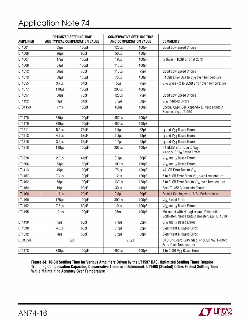
The simplest way to summarize the four different method’sresults is by visual comparison. Figures 30 through 33repeat previous photos of the four different settling-timemethods. If all four approaches represent good measure-ment technique and are constructed properly, resultsshould be indentical.15 If this is the case, the identical dataproduced by the four methods has a high probability ofbeing valid.
Examination of the four photographs shows identical1.7µs settling times and settling waveform signatures.The shape of the settling waveform, in every detail, isidentical in all four photos. This kind of agreement pro-vides a high degree of credibility to the measured results.It also provides the confidence necessary to characterizea wide variety of amplifiers. Figure 34 lists various LTCamplifiers and their measured settling times to 16 bits.
500ns/DIVAN74 F30
B = 500µV/DIV
A = 5V/DIV
Figure 30. DAC Settling Time Measurement Usingthe Sampling Bridge Circuit. tSETTLE = 1.7µs
500ns/DIVAN74 F31
Figure 31. DAC Settling Time Measurement with theBootstrapped Clamp Method. tSETTLE = 1.7µs
A = 5V/DIV
B = 500µV/DIV
500ns/DIVAN74 F32
Figure 32. DAC Settling Time Measurement Usingthe Classical Sampling ‘Scope. tSETTLE = 1.7µs
500ns/DIVAN74 F33
Figure 33. DAC Settling Time Measurement with theDifferential Amplifier. tSETTLE = 1.7µs
A = 5V/DIV
B = 500µV/DIV
A = 5V/DIV
B = 500µV/DIV
DAC Settling Time Measurement Using Four Different Methods. Waveform Signatures and Settling Times Appear Identical
About This Chart
The writer despises charts. In their attempt to gain author-ity they simplify, and glib simplification is the host ofmother nature’s surprise party. Any topic as complex asDAC-amplifier settling time to 16 bits is a dangerous placefor oversimplification. There are simply too many vari-ables and exceptions to accommodate the categoricalstatement a chart implies. It is with these reservations thatFigure 34 is presented.16 The chart lists measured settlingtimes to 16 bits for various LTC amplifiers used with theLTC1595-7 16-bit DACs. A number of conditions andcomments apply to interpreting the chart’s information.
Note 15: Construction details of the settling time fixtures discussedhere appear (literally) in Appendix G, “Breadboarding, Layout andConnection Techniques.”Note 16: Readers detecting author ambivalence about the inclusion ofFigure 34’s chart are not hallucinating.
Application Note 74
AN74-16
OPTIMIZED SETTLING TIME CONSERVATIVE SETTLING TIMEAMPLIFIER AND TYPICAL COMPENSATION VALUE AND COMPENSATION VALUE COMMENTS
LT1001 65µs 100pF 120µs 100pF Good Low Speed Choice
LT1006 26µs 66pF 50µs 150pF
LT1007 17µs 100pF 19µs 100pF IB Gives ≈1LSB Error at 25°C
LT1008 64µs 100pF 115µs 100pF
LT1012 56µs 75pF 116µs 75pF Good Low Speed Choice
LT1013 50µs 150pF 75µs 150pF ≈1LSB Error Due to VOS over Temperature
LT1055 3.7µs 54pF 5µs 75pF VOS Gives ≈2 to 3LSB Error over Temperature
LT1077 110µs 100pF 200µs 100pF
LT1097 60µs 75pF 120µs 75pF Good Low Speed Choice
LT1122 3µs 51pF 3.5µs 68pF VOS Induced Errors
LTC1150 7ms 100pF 10ms 100pF Special Case. See Appendix E. Needs OutputBooster, e.g., LT1010
LT1178 330µs 100pF 450µs 100pF
LT1179 330µs 100pF 450µs 100pF
LT1211 5.5µs 73pF 6.5µs 82pF IB and VOS Based Errors
LT1213 4.6µs 58pF 5.8µs 68pF IB and VOS Based Errors
LT1215 3.6µs 53pF 4.7µs 68pF IB and VOS Based Errors
LT1218 110µs 100pF 200µs 100pF ≈1.5LSB Error Due to VOS.≈4 to 5LSB IB Based Errors
LT1220 2.3µs 41pF 3.1µs 56pF VOS and IB Based Errors
LT1366 64µs 100pF 100µs 150pF VOS and IB Based Errors
LT1413 45µs 100pF 75µs 120pF ≈2LSB Error Due to VOS
LT1457 7.4µs 100pF 12µs 120pF 5 to 6LSB Error From VOS over Temperature
LT1462 78µs 100pF 130µs 120pF 7 to 8LSB Error Due to VOS over Temperature
LT1464 19µs 90pF 30µs 110pF See LT1462 Comments Above
LT1468 1.7µs 20pF 2.5µs 30pF Fastest Settling with 16-Bit Performance
LT1490 175µs 100pF 300µs 100pF VOS Based Errors
LT1492 7.5µs 80pF 10µs 100pF VOS and IB Based Errors
LT1495 10ms 100pF 25ms 100pF Measured with Hourglass and DifferentialVoltmeter. Needs Output Booster, e.g., LT1010
LT1498 5µs 60pF 7.3µs 82pF VOS and IB Based Errors
LT1630 4.5µs 63pF 6.7µs 82pF Significant IB Based Error
LT1632 4µs 55pF 5.2µs 68pF Significant IB Based Error
LTC1650 6µs 7.3µs DAC On-Board. ±4V Step. ≈10LSB VOS RelatedError Over Temperature
LT2178 330µs 100pF 450µs 100pF 1 to 2LSB VOS Based Error
Figure 34. 16-Bit Settling Time for Various Amplifiers Driven by the LT1597 DAC. Optimized Settling Times RequireTrimming Compensation Capacitor, Conservative Times are Untrimmed. LT1468 (Shaded) Offers Fastest Settling TimeWhile Maintaining Accuracy Over Temperature

Application Note 74
AN74-17
The amplifiers selected are not all accurate to 16 bits overtemperature, or (in some cases) even at 25°C. However,many applications, such as AC signal processing, servoloops or waveform generation, are insensitive to DC offseterror and, as such, these amplifiers are worthy candidates.Applications requiring DC accuracy to 16 bits (10V fullscale) must keep input errors below 15nA and 152µV tomaintain performance.
The settling times are quoted for “optimized” and “con-servative” cases. The optimized case uses a typical ampli-fier-DAC combination. This implies “design centered”values for amplifier slew rate and DAC output resistanceand capacitance. It also permits trimming the amplifier’sfeedback capacitor to obtain the best possible settlingtime. The conservative category assumes worst-caseamplifier slew rate, highest DAC output impedances anduntrimmed, standard 5% feedback capacitors. This worst-case error summation is perhaps unduly pessimistic;RMS summing may represent a more realistic compro-mise. However, such a maudlin outlook helps avoidunpleasant surprises in production. Settling times arequoted using ±15V supplies, a –10V DAC reference and a10V positive output step. The sole exception to this is theLTC1650, a 16-bit DAC with amplifier onboard. Thisdevice is powered by ±5V supplies and settling is mea-sured with a 4V reference and a ±4V swing.17 All feedbackcapacitances listed were determined with a General Radiomodel 1422-CL precision variable air capacitor.18
In general, the slower amplifiers’ extended slew timesmake their ring times vanishingly small settling-time con-tributors. This is reflected in identical feedback capacitorvalues for the optimized and conservative cases. Con-versely, faster amplifiers’ ring times are significant terms,resulting in different compensation values for the twocategories. Additional considerations for compensationare discussed in Appendix D, “Practical Considerations forDAC-Amplifier Compensation.”
Thermally Induced Settling Errors
A final category of settling-time error is thermally based.Some poorly designed amplifiers exhibit a substantial“thermal tail” after responding to an input step. Thisphenomenon, due to die heating, can cause the output towander outside desired limits long after settling has ap-parently occurred. After checking settling at high speed itis always a good idea to slow the oscilloscope sweep downand look for thermal tails. Figure 35 shows such a tail. Theamplifier slowly (note horizontal sweep speed) drifts 200µVafter settling has apparently occurred. Often, the thermaltail’s effect can be accentuated by loading the amplifier’soutput. Figure 36 doubles the error by increasing amplifierloading.
1ms/DIVAN74 F35
B = 500µV/DIV
A = 5V/DIV
Figure 35. Typical Thermal Tail in a Poorly Designed Amplifier.Device Drifts 200µV (>1LSB) After Settling Apparently Occurs
1ms/DIVAN74 F36
B = 500µV/DIV
A = 5V/DIV
Figure 36. Loading the Amplifier IncreasesThermal Tail Error to 400µV (>2.5LSB)
Note 17: See Appendix F, “Settling Time Measurement of SeriallyLoaded DACs.”Note 18: A thing of transcendent beauty. It is worth owning thisinstrument just to look at it. It is difficult to believe humanity couldfashion anything so perfectly gorgeous.

Application Note 74
AN74-18
REFERENCES
1. Williams, Jim, “Methods for Measuring Op AmpSettling Time,” Linear Technology Corporation,Application Note 10, July 1985.
2. Demerow, R., “Settling Time of Operational Amplifi-ers,” Analog Dialogue, Volume 4-1, Analog Devices,Inc., 1970.
3. Pease, R. A., “The Subtleties of Settling Time,” TheNew Lightning Empiricist, Teledyne Philbrick, June1971.
4. Harvey, Barry, “Take the Guesswork Out of SettlingTime Measurements,” EDN, September 19, 1985.
5. Williams, Jim, “Settling Time MeasurementDemands Precise Test Circuitry,” EDN, November15, 1984.
6. Schoenwetter, H. R., “High-Accuracy Settling TimeMeasurements,” IEEE Transactions on Instrumenta-tion and Measurement, Vol. IM-32. No. 1, March1983.
7. Sheingold, D. H., “DAC Settling Time Measure-ment,” Analog-Digital Conversion Handbook, pg312-317. Prentice-Hall, 1986.
8. Williams, Jim, “Evaluating Oscilloscope OverloadPerformance,” Box Section A, in “Methods forMeasuring Op Amp Settling Time,” Linear Technol-ogy Corporation, Application Note 10, July 1985.
9. Orwiler, Bob, “Oscilloscope Vertical Amplifiers,”Tektronix, Inc., Concept Series, 1969.
10. Addis, John, “Fast Vertical Amplifiers and GoodEngineering,” Analog Circuit Design; Art, Scienceand Personalities, Butterworths, 1991.
11. W. Travis, “Settling Time Measurement UsingDelayed Switch,” Private Communication. 1984.
12. Hewlett-Packard, “Schottky Diodes for High-Volume, Low Cost Applications,” Application Note942, Hewlett-Packard Company, 1973.
13. Harris Semiconductor, “CA3039 Diode Array DataSheet, Harris Semiconductor, 1993.
14. Carlson, R., “A Versatile New DC-500MHz Oscillo-scope with High Sensitivity and Dual ChannelDisplay,” Hewlett-Packard Journal, Hewlett-PackardCompany, January 1960.
15. Tektronix, Inc., “Sampling Notes,” Tektronix, Inc.,1964.
16. Tektronix, Inc., “Type 1S1 Sampling Plug-In Operat-ing and Service Manual,” Tektronix, Inc., 1965.
17. Mulvey, J., “Sampling Oscilloscope Circuits,”Tektronix, Inc., Concept Series, 1970.
18. Addis, John, “Sampling Oscilloscopes,” PrivateCommunication, February, 1991.
19. Williams, Jim, “Bridge Circuits—Marrying Gain andBalance,” Linear Technology Corporation, Applica-tion Note 43, June, 1990.
20. Tektronix, Inc., “Type 661 Sampling OscilloscopeOperating and Service Manual,’ Tektronix, Inc.,1963.
21. Tektronix, Inc., “Type 4S1 Sampling Plug-In Operat-ing and Service Manual,” Tektronix, Inc., 1963.
22. Tektronix, Inc., “Type 5T3 Timing Unit Operatingand Service Manual,” Tektronix, Inc., 1965.
23. Williams, Jim, “Applications Considerations andCircuits for a New Chopper-Stabilized Op Amp,”Linear Technology Corporation, Application Note 9,March, 1985.
24. Morrison, Ralph, “Grounding and Shielding Tech-niques in Instrumentation,” 2nd Edition, WileyInterscience, 1977.
25. Ott, Henry W., “Noise Reduction Techniques inElectronic Systems,” Wiley Interscience, 1976.
26. Williams, Jim, “High Speed Amplifier Techniques,”Linear Technology Corporation, Application Note47, 1991.
27. Williams, Jim, “Power Gain Stages for MonolithicAmplifiers,” Linear Technology Corporation, Appli-cation Note 18, March 1986.

Application Note 74
AN74-19
APPENDIX A
A HISTORY OF HIGH ACCURACYDIGITAL-TO-ANALOG CONVERSION
People have been converting digital-to-analog quantitiesfor a long time. Probably among the earliest uses was thesumming of calibrated weights (Figure A1, left center) inweighing applications. Early electrical digital-to-analogconversion inevitably involved switches and resistors ofdifferent values, usually arranged in decades. The applica-tion was often the calibrated balancing of a bridge orreading, via null detection, some unknown voltage. Themost accurate resistor-based DAC of this type is LordKelvin’s Kelvin-Varley divider (Figure, large box). Basedon switched resistor ratios, it can achieve ratio accuraciesof 0.1ppm (23+ bits) and is still widely employed instandards laboratories. High speed digital-to-analog con-version resorts to electronically switching the resistornetwork. Early electronic DACs were built at the board levelusing discrete precision resistors and germanium transis-tors (Figure, center foreground, is a 12-bit DAC from a
Minuteman missile D-17B inertial navigation system, circa1962). The first electronically switched DACs available asstandard product were probably those produced byPastoriza Electronics in the mid 1960s. Other manufactur-ers followed and discrete- and monolithically-based modu-lar DACs (Figure, right and left) became popular by the1970s. The units were often potted (Figure, left) forruggedness, performance or to (hopefully) preserve pro-prietary knowledge. Hybrid technology produced smallerpackage size (Figure, left foreground). The development ofSi-Chrome resistors permitted precision monolithic DACssuch as the LTC1595 (Figure, immediate foreground). Inkeeping with all things monolithic, the cost-performancetrade off of modern high resolution IC DACs is a bargain.Think of it! A 16-bit DAC in an 8-pin IC package. What LordKelvin would have given for a credit card and LTC’s phonenumber.
Figure A1. Historically Significant Digital-to-Analog Converters Include: Weight Set (Center Left), 23+ Bit Kelvin-Varley Divider(Large Box), Hybrid, Board and Modular Types, and the LTC1595 IC (Foreground). Where Will It All End?

Application Note 74
AN74-20
APPENDIX B
EVALUATING OSCILLOSCOPE OVERDRIVEPERFORMANCE
Most of the settling-time circuits are heavily oriented to-wards providing little or no overdrive to the monitoringoscilloscope. This is done to avoid overdriving the oscil-loscope. Oscilloscope recovery from overdrive is a greyarea and almost never specified. Some of the settling timemeasurement methods require the oscilloscope to beoverdriven. In these cases, the oscilloscope is required tosupply an accurate waveform after the display has beendriven off screen. How long must one wait after an over-drive before the display can be taken seriously? The an-swer to this question is quite complex. Factors involvedinclude the degree of overdrive, its duty cycle, its magni-tude in time and amplitude and other considerations. Os-cilloscope response to overdrive varies widely betweentypes and markedly different behavior can be observed inany individual instrument. For example, the recovery timefor a 100× overload at 0.005V/DIV may be very differentthan at 0.1V/DIV. The recovery characteristic may also varywith waveform shape, DC content and repetition rate. Withso many variables, it is clear that measurements involvingoscilloscope overdrive must be approached with caution.
Why do most oscilloscopes have so much trouble recov-ering from overdrive? The answer to this questionrequires some study of the three basic oscilloscope types’vertical paths. The types include analog (Figure B1A),digital (Figure B1B) and classical sampling (Figure B1C)oscilloscopes. Analog and digital ‘scopes are susceptibleto overdrive. The classical sampling ‘scope is the onlyarchitecture that is inherently immune to overdrive.
An analog oscilloscope (Figure B1A) is a real time, con-tinuous linear system.1 The input is applied to an attenu-ator, which is unloaded by a wideband buffer. The verticalpreamp provides gain, and drives the trigger pick-off,delay line and the vertical output amplifier. The attenuatorand delay line are passive elements and require littlecomment. The buffer, preamp and vertical output ampli-fier are complex linear gain blocks, each with dynamicoperating range restrictions. Additionally, the operatingpoint of each block may be set by inherent circuit balance,low frequency stabilization paths or both. When the inputis overdriven, one or more of these stages may saturate,
forcing internal nodes and components to abnormal oper-ating points and temperatures. When the overload ceases,full recovery of the electronic and thermal time constantsmay require surprising lengths of time.2
The digital sampling oscilloscope (Figure B1B) eliminatesthe vertical output amplifier, but has an attenuator bufferand amplifiers ahead of the A/D converter. Because of this,it is similarly susceptible to overdrive recovery problems.
The classical sampling oscilloscope is unique. Its natureof operation makes it inherently immune to overload. Fig-ure B1C shows why. The sampling occurs before any gainis taken in the system. Unlike Figure B1B’s digitally sampled‘scope, the input is fully passive to the sampling point.Additionally, the output is fed back to the sampling bridge,maintaining its operating point over a very wide range ofinputs. The dynamic swing available to maintain the bridgeoutput is large and easily accommodates a wide range ofoscilloscope inputs. Because of all this, the amplifiers inthis instrument do not see overload, even at 1000× over-drives, and there is no recovery problem. Additional im-munity derives from the instrument’s relatively slow samplerate—even if the amplifiers were overloaded, they wouldhave plenty of time to recover between samples.3
The designers of classical sampling ‘scopes capitalized onthe overdrive immunity by including variable DC offsetgenerators to bias the feedback loop (see Figure B1C,lower right). This permits the user to offset a large input,so small amplitude activity on top of the signal can beaccurately observed. This is ideal for, among other things,settling time measurements. Unfortunately, classical sam-pling oscilloscopes are no longer manufactured, so if youhave one, take care of it!
Note 1: Ergo, the Real Thing. Hopelessly bigoted residents of thislocale mourn the passing of the analog ‘scope era and frantically hoardevery instrument they can find.Note 2: Some discussion of input overdrive effects in analog oscillo-scope circuitry is found in reference 10.Note 3: Additional information and detailed treatment of classicalsampling oscilloscope operation appears in references 14-17 and20-22.

Application Note 74
AN74-21
Figure B1. Simplified Vertical Channel Diagrams for Different Type Oscilloscopes. Only the Classical Sampling ‘Scope (C)Has Inherent Overdrive Immunity. Offset Generator Allows Viewing Small Signals Riding On Large Excursions
Although analog and digital oscilloscopes are susceptibleto overdrive, many types can tolerate some degree of thisabuse. The early portion of this appendix stressed thatmeasurements involving oscilloscope overdrive must beapproached with caution. Nevertheless, a simple test canindicate when the oscilloscope is being deleteriously af-fected by overdrive.
The waveform to be expanded is placed on the screen at avertical sensitivity that eliminates all off-screen activity.Figure B2 shows the display. The lower right hand portionis to be expanded. Increasing the vertical sensitivity by afactor of two (Figure B3) drives the waveform off-screen,but the remaining display appears reasonable. Amplitudehas doubled and waveshape is consistent with the original
INPUT ATTENUATOR ATTENUATOR
BUFFER
ATTENUATOR BUFFER
A ANALOG
OSCILLOSCOPE VERTICAL CHANNEL
V+
V –
DELAY LINE
TRIGGER CIRCUITRY
VERTICAL PREAMP
VERTICAL OUTPUT
TO HORIZONTAL/ SWEEP SECTION
TO CRT
INPUT ATTENUATOR
B DIGITAL
SAMPLING OSCILLOSCOPE
VERTICAL CHANNEL
C CLASSICAL SAMPLING
OSCILLOSCOPE VERTICAL CHANNEL
V+
V –
A/D
DELAY LINE
TO HORIZONTAL CIRCUITS
INPUT
FEEDBACK
TRIGGER CIRCUITRY
DC OFFSET GENERATOR
PULSE STRETCHER— MEMORY SWITCH
DRIVER
V+
A/D CONTROL
MEMORY
TIMING GENERATOR
MICROPROCESSOR
TRIGGER CIRCUITRY
VERTICAL PREAMP
VERTICAL AMPLIFIER
AC AMPLIFIER
A/D DRIVER AMP
SAMPLE COMMAND
TO CRT
TO CRT
AN74 FB1
MEMORYV –
V – V+

Application Note 74
AN74-22
display. Looking carefully, it is possible to see smallamplitude information presented as a dip in the waveformat about the third vertical division. Some small distur-bances are also visible. This observed expansion of theoriginal waveform is believable. In Figure B4, gain hasbeen further increased, and all the features of Figure B3 areamplified accordingly. The basic waveshape appears clearerand the dip and small disturbances are also easier to see.No new waveform characteristics are observed. Figure B5
Figures B2-B7. The Overdrive Limit is Determined by ProgressivelyIncreasing Oscilloscope Gain and Watching for Waveform Aberrations
100ns/DIVAN74 FB2
Figure B2
A = 1V/DIV
100ns/DIVAN74 FB3
Figure B3
A = 0.5V/DIV
100ns/DIVAN74 FB4
Figure B4
A = 0.2V/DIV
100ns/DIVAN74 FB5
Figure B5
100ns/DIVAN74 FB6
Figure B6
A = 0.1V/DIV
100ns/DIVAN74 FB7
A = 0.1V/DIV
Figure B7
A = 0.1V/DIV
brings some unpleasant surprises. This increase in gaincauses definite distortion. The initial negative-going peak,although larger, has a different shape. Its bottom appearsless broad than in Figure B4. Additionally, the peak’spositive recovery is shaped slightly differently. A newrippling disturbance is visible in the center of the screen.This kind of change indicates that the oscilloscope ishaving trouble. A further test can confirm that this wave-form is being influenced by overloading. In Figure B6 the

Application Note 74
AN74-23
gain remains the same but the vertical position knob hasbeen used to reposition the display at the screen’s bottom.This shifts the oscilloscope’s DC operating point which,under normal circumstances, should not affect the dis-played waveform. Instead, a marked shift in waveform
amplitude and outline occurs. Repositioning the wave-form to the screen’s top produces a differently distortedwaveform (Figure B7). It is obvious that for this particularwaveform, accurate results cannot be obtained at thisgain.
APPENDIX C
MEASURING AND COMPENSATINGRESIDUE-AMPLIFIER DELAY
The settling-time circuits utilize an adjustable delay net-work to time correct the input pulse for delays in thesignal-processing path. Typically, these delays introduceerrors of a few percent, so a first-order correction isadequate. Setting the delay trim involves observing thenetwork’s input-output delay and adjusting for the appro-priate time interval. Determining the “appropriate” timeinterval is somewhat more complex. Measuring the sam-pling bridge-based circuit’s signal path delay involvesmodifications to Figure 6, shown in Figure C1. Thesechanges lock the circuit into its “sample” mode, permit-ting an input-to-output delay measurement under signal-level conditions similar to normal operation. In Figure C2,trace A is the pulse-generator input at 200µV/DIV (note10k-1Ω divider feeding the settle node). Trace B shows thecircuit output at A2, delayed by about 12ns. This delay isa small error, but is readily corrected by adjusting the delaynetwork for the same time lag.
Figure C3 takes a similar approach with Figure 26’s sam-pling ‘scope-based measurement. Modifications permit asmall amplitude pulse to drive the settle node, mimickingnormal operation signal level conditions. Circuit output atA2 is monitored for delay with respect to the input pulse.Note that A2’s high impedance output requires a FETprobe to avoid loading. As such, the input pulse must berouted to the oscilloscope via a similar FET probe tomaintain delay matching. Figure C4 shows results. Theoutput (trace B) lags the input by 32ns. This factor is usedto calibrate text Figure 26’s delay network, compensatingthe circuit’s signal path propagation time error.
Delay compensation values for the bootstrapped clamp(text Figure 24) and differential amplifier (text Figure 28)circuits were determined in similar fashion.
Application Note 74
AN74-24
+
7
11 D5
AC COMP 2.5k
RESIDUE AMPLIFIER SETTLE NODE
×20 OUTPUT TO OSCILLOSCOPE 0.01V/DIV = 500µV/DIV AT DAC AMPLIFIER OUTPUT
SAMPLING BRIDGE
108
4
14
1.1k
Q1
D7
Q4
11
1013
8
7
9 6Q3
5pF
3pF
0.1µF 10µF
510Ω
D633Ω*
1.3k*
Q2
CA3039 ARRAY
GROUND THIS
POINT
121 13
–5V
–5V
–5V
SKEW COMP 2.5k
3
2 5
3k**SETTLE NODE
3k**2.2k1.1k
5V
2.2k 10µF 0.1µF
470Ω
560Ω
51Ω820Ω 51Ω680Ω
500Ω BASELINE
ZERO
1.5k
–
+A2
LT1222
0.1µF 10µF+
+
VCC RC1
5k WIDTH
5V
SAMPLE WINDOW WIDTH SAMPLE DELAY/ WINDOW GENERATOR
5V
5V
5V
4.7k
4.7k
20k DELAY
1000pF
5.1k
C1 Q1
74HC123
Q2 CLR2 B2 A2
A1 B1 CLR1 Q1 Q2 C2 RC2 GND
470pF
AN74 FC1
5.1k
SAMPLING BRIDGE DRIVER
OUTPUT TO OSCILLOSCOPE
15V
–15VD8
DISCONNECT
D9
–
+
A1 LT1220
10k5V PULSE INPUT
1Ω
A = 200µV/DIV
B = 10mV/DIV
10ns/DIVAN74 FC2
Figure C2. Input-Output Delay for SamplingBridge Circuit Measures About 12ns
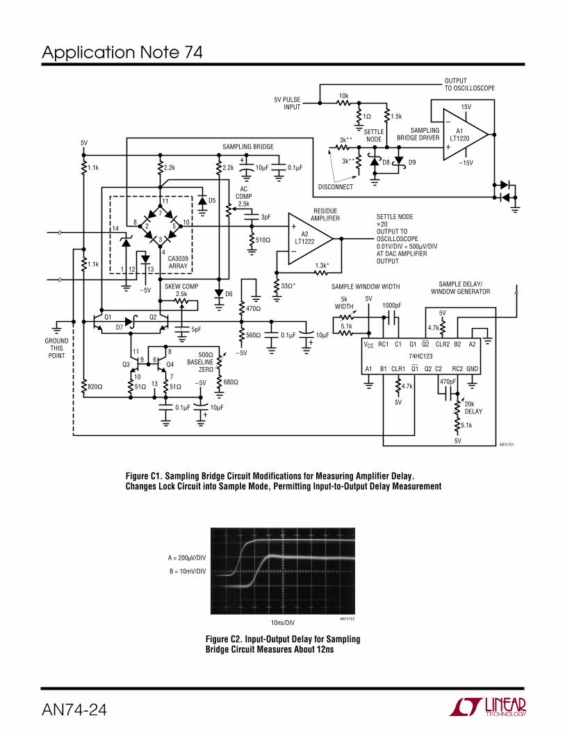
Figure C1. Sampling Bridge Circuit Modifications for Measuring Amplifier Delay.Changes Lock Circuit into Sample Mode, Permitting Input-to-Output Delay Measurement

Application Note 74
AN74-25
AN74 FC3
–
+A1
LT1221
3k*
1.5k
1.5k
422Ω*
–
+
3k*
OUTPUT TO SAMPLING OSCILLOSCOPE VIA FET PROBE
USE SAME TYPE FET PROBE FOR BOTH OUTPUTS TO ENSURE DELAY MATCHING
5V PULSE INPUT
332Ω*
OUTPUT TO OSCILLOSCOPE VIA FET PROBE
3k
1.5k1Ω
3k
10k
DISCONNECT
A2 LT1222
A = 200µV/DIV
B = 10mV/DIV
20ns/DIVAN74 FC4
Figure C4. Delay Measurement Results for Figure C3.Input-Output Time Lag is About 32ns
Figure C3. Partial Version of Figure 26 Showing Modifications Permitting DelayTime Measurment. FET Probes are the Same Type, Eliminating Time Skewing Error
Application Note 74
AN74-26
APPENDIX D
PRACTICAL CONSIDERATIONS FOR DAC-AMPLIFIERCOMPENSATION
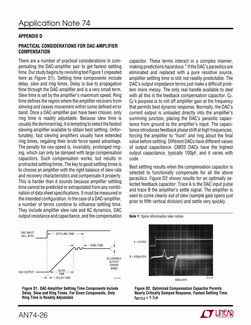
There are a number of practical considerations in com-pensating the DAC-amplifier pair to get fastest settlingtime. Our study begins by revisiting text Figure 1 (repeatedhere as Figure D1). Settling time components includedelay, slew and ring times. Delay is due to propagationtime through the DAC-amplifier and is a very small term.Slew time is set by the amplifier’s maximum speed. Ringtime defines the region where the amplifier recovers fromslewing and ceases movement within some defined errorband. Once a DAC-amplifier pair have been chosen, onlyring time is readily adjustable. Because slew time isusually the dominant lag, it is tempting to select the fastestslewing amplifier available to obtain best settling. Unfor-tunately, fast slewing amplifiers usually have extendedring times, negating their brute force speed advantage.The penalty for raw speed is, invariably, prolonged ring-ing, which can only be damped with large compensationcapacitors. Such compensation works, but results inprotracted settling times. The key to good settling times isto choose an amplifier with the right balance of slew rateand recovery characteristics and compensate it properly.This is harder than it sounds because amplifier settlingtime cannot be predicted or extrapolated from any combi-nation of data sheet specifications. It must be measured inthe intended configuration. In the case of a DAC-amplifier,a number of terms combine to influence settling time.They include amplifier slew rate and AC dynamics, DACoutput resistance and capacitance, and the compensation
capacitor. These terms interact in a complex manner,making predictions hazardous.1 If the DAC’s parasitics areeliminated and replaced with a pure resistive source,amplifier settling time is still not readily predictable. TheDAC’s output impedance terms just make a difficult prob-lem more messy. The only real handle available to dealwith all this is the feedback compensation capacitor, CF.CF’s purpose is to roll off amplifier gain at the frequencythat permits best dynamic response. Normally, the DAC’scurrent output is unloaded directly into the amplifier’ssumming junction, placing the DAC’s parasitic capaci-tance from ground to the amplifier’s input. The capaci-tance introduces feedback phase shift at high frequencies,forcing the amplifier to “hunt” and ring about the finalvalue before settling. Different DACs have different valuesof output capacitance. CMOS DACs have the highestoutput capacitance, typically 100pF, and it varies withcode.
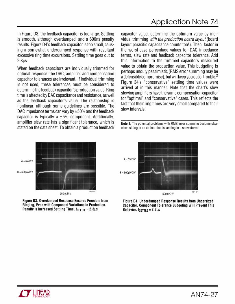
Best settling results when the compensation capacitor isselected to functionally compensate for all the aboveparasitics. Figure D2 shows results for an optimally se-lected feedback capacitor. Trace A is the DAC input pulseand trace B the amplifier’s settle signal. The amplifier isseen to come cleanly out of slew (sample gate opens justprior to fifth vertical division) and settle very quickly.
DAC INPUT (ALL BITS)
DAC OUTPUT
AN74 D01
SETTLING TIME
SLEW TIME
RING TIME
ALLOWABLE OUTPUT ERROR BAND
DELAY TIME
Figure D2. Optimized Compensation Capacitor PermitsNearly Critically Damped Response, Fastest Settling Time.tSETTLE = 1.7µs
A = 5V/DIV
B = 500µV/DIV
500ns/DIVAN74 FD2
Note 1: Spice aficionados take notice.
Figure D1. DAC-Amplifier Settling Time Components IncludeDelay, Slew and Ring Times. For Given Components, OnlyRing Time is Readily Adjustable
Application Note 74
AN74-27
In Figure D3, the feedback capacitor is too large. Settlingis smooth, although overdamped, and a 600ns penaltyresults. Figure D4’s feedback capacitor is too small, caus-ing a somewhat underdamped response with resultantexcessive ring time excursions. Settling time goes out to2.3µs.
When feedback capacitors are individually trimmed foroptimal response, the DAC, amplifier and compensationcapacitor tolerances are irrelevant. If individual trimmingis not used, these tolerances must be considered todetermine the feedback capacitor’s production value. Ringtime is affected by DAC capacitance and resistance, as wellas the feedback capacitor’s value. The relationship isnonlinear, although some guidelines are possible. TheDAC impedance terms can vary by ±50% and the feedbackcapacitor is typically a ±5% component. Additionally,amplifier slew rate has a significant tolerance, which isstated on the data sheet. To obtain a production feedback
capacitor value, determine the optimum value by indi-vidual trimming with the production board layout (boardlayout parasitic capacitance counts too!). Then, factor inthe worst-case percentage values for DAC impedanceterms, slew rate and feedback capacitor tolerance. Addthis information to the trimmed capacitors measuredvalue to obtain the production value. This budgeting isperhaps unduly pessimistic (RMS error summing may bea defensible compromise), but will keep you out of trouble.2Figure 34’s “conservative” settling time values werearrived at in this manner. Note that the chart’s slowslewing amplifiers have the same compensation capacitorfor “optimal” and “conservative” cases. This reflects thefact that their ring times are very small compared to theirslew intervals.
Note 2: The potential problems with RMS error summing become clearwhen sitting in an airliner that is landing in a snowstorm.
B = 500µV/DIV
500ns/DIVAN74 FD3
A = 5V/DIV
Figure D3. Overdamped Response Ensures Freedom fromRinging, Even with Component Variations in Production.Penalty is Increased Settling Time. tSETTLE = 2.3µs
500ns/DIVAN74 FD4
A = 5V/DIV
B = 500µV/DIV
Figure D4. Underdamped Response Results from UndersizedCapacitor. Component Tolerance Budgeting Will Prevent ThisBehavior. tSETTLE = 2.3µs
Application Note 74
AN74-28
APPENDIX E
A VERY SPECIAL CASE—MEASURING SETTLING TIMEOF CHOPPER-STABILIZED AMPLIFIERS
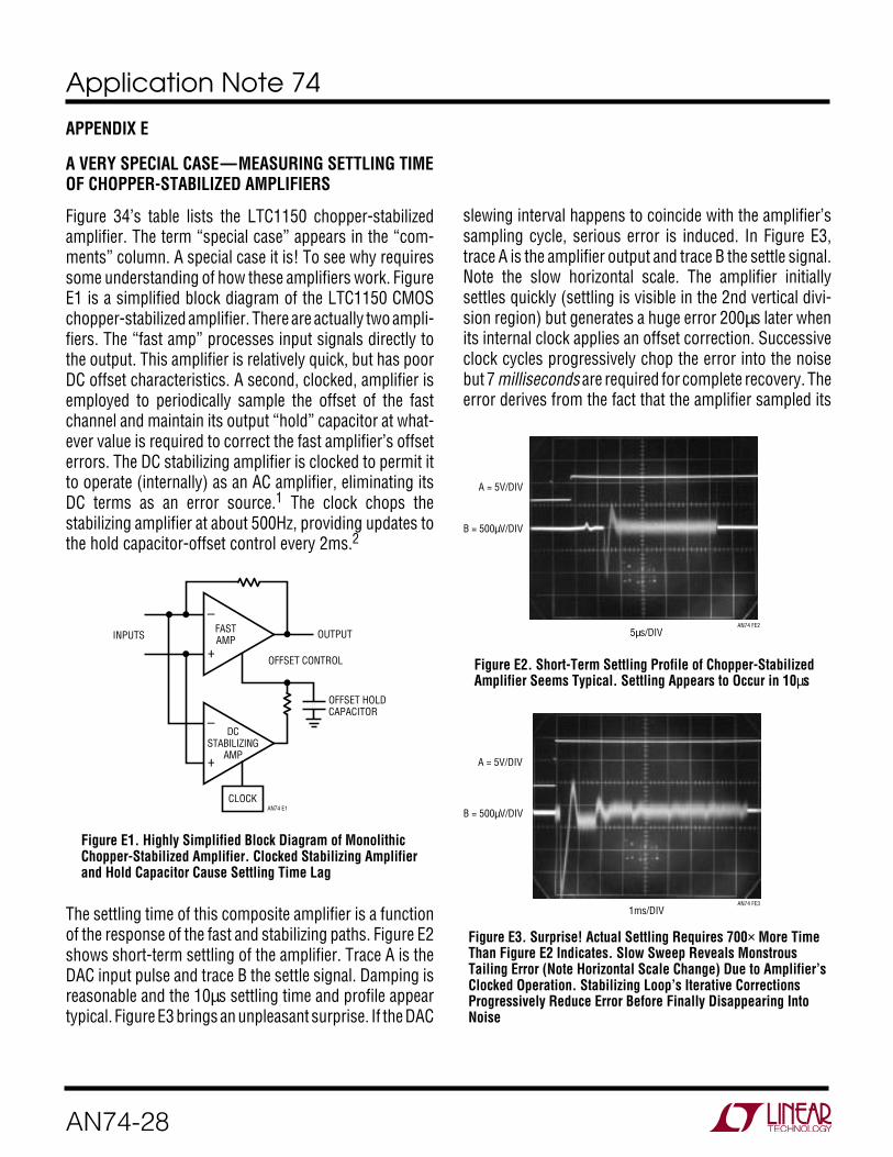
Figure 34’s table lists the LTC1150 chopper-stabilizedamplifier. The term “special case” appears in the “com-ments” column. A special case it is! To see why requiressome understanding of how these amplifiers work. FigureE1 is a simplified block diagram of the LTC1150 CMOSchopper-stabilized amplifier. There are actually two ampli-fiers. The “fast amp” processes input signals directly tothe output. This amplifier is relatively quick, but has poorDC offset characteristics. A second, clocked, amplifier isemployed to periodically sample the offset of the fastchannel and maintain its output “hold” capacitor at what-ever value is required to correct the fast amplifier’s offseterrors. The DC stabilizing amplifier is clocked to permit itto operate (internally) as an AC amplifier, eliminating itsDC terms as an error source.1 The clock chops thestabilizing amplifier at about 500Hz, providing updates tothe hold capacitor-offset control every 2ms.2
–
+FAST AMPINPUTS OUTPUT
OFFSET CONTROL
AN74 E1
–
+
DC STABILIZING
AMP
OFFSET HOLD CAPACITOR
CLOCK
Figure E1. Highly Simplified Block Diagram of MonolithicChopper-Stabilized Amplifier. Clocked Stabilizing Amplifierand Hold Capacitor Cause Settling Time Lag
The settling time of this composite amplifier is a functionof the response of the fast and stabilizing paths. Figure E2shows short-term settling of the amplifier. Trace A is theDAC input pulse and trace B the settle signal. Damping isreasonable and the 10µs settling time and profile appeartypical. Figure E3 brings an unpleasant surprise. If the DAC
slewing interval happens to coincide with the amplifier’ssampling cycle, serious error is induced. In Figure E3,trace A is the amplifier output and trace B the settle signal.Note the slow horizontal scale. The amplifier initiallysettles quickly (settling is visible in the 2nd vertical divi-sion region) but generates a huge error 200µs later whenits internal clock applies an offset correction. Successiveclock cycles progressively chop the error into the noisebut 7 milliseconds are required for complete recovery. Theerror derives from the fact that the amplifier sampled its
A = 5V/DIV
B = 500µV/DIV
5µs/DIVAN74 FE2
1ms/DIVAN74 FE3
A = 5V/DIV
B = 500µV/DIV
Figure E3. Surprise! Actual Settling Requires 700× More TimeThan Figure E2 Indicates. Slow Sweep Reveals MonstrousTailing Error (Note Horizontal Scale Change) Due to Amplifier’sClocked Operation. Stabilizing Loop’s Iterative CorrectionsProgressively Reduce Error Before Finally Disappearing IntoNoise
Figure E2. Short-Term Settling Profile of Chopper-StabilizedAmplifier Seems Typical. Settling Appears to Occur in 10µs

Application Note 74
AN74-29
offset when its input was driven well outside its bandpass.This caused the stabilizing amplifier to acquire erroneousoffset information. When this “correction” was applied,the result was a huge output error.
This is admittedly a worst case. It can only happen if theDAC slewing interval coincides with the amplifier’s inter-nal clock cycle, but it can happen.3, 4
Note 1: This AC processing of DC information is the basis of allchopper and chopper-stabilized amplifiers. In this case, if we couldbuild an inherently stable CMOS amplifier for the stabilizing stage, nochopper stabilization would be necessary.Note 2: Those finding this description intolerably brief are commendedto reference 23.Note 3: Readers are invited to speculate on the instrumentationrequirements for obtaining Figure E3’s photo.Note 4: The spirit of Appendix D’s footnote 2 is similarly applicable inthis instance.
APPENDIX F
SETTLING TIME MEASUREMENT OFSERIALLY LOADED DACS
LTC models LTC1595 and LTC1650 are serially loaded16-bit DACs. The LTC1650 includes an onboard outputamplifier. Measuring these device’s settling time with themethods described in the text requires additional circuitry.The circuitry must provide a “start” pulse to the settlingtime measurement after serially loading a full-scale stepinto the DAC. Figure F1’s circuitry, designed and con-structed by Jim Brubaker, Kevin Hoskins, Hassan Malikand Tuyet Pham (all of LTC) does this. The “start” pulse istaken from U1B’s Q output. The DAC amplifier is moni-
tored in the normal manner. This permits Figure F2 todisplay settling results in (what should be by now) familiarfashion. Settling time (trace B) is measured from the risingedge of trace A’s start pulse. Figure F3 is a similar circuitconfigured for the LTC1650 voltage output DAC. Refer-ence voltage and other changes are required to accommo-date the DAC’s ±4V output swing and different architecture,but overall operation is similar. Figure F4 shows settlingresults.

Application Note 74
AN74-30
U1A 74HC123 U2
74HC132U3
74HC04
7
5V
5V
5V
0.1µF
6
12
5 54
16
8
9Q
U1B 74HC123
Q
10
123 1 2
6
1414
6
7, 12, 13 7, 11, 1311
1.6k
120pF
12k
U2
5V
U3
U3
11
12
93 4
10
8
7 13
5V
U4 74HC74
CLKPR
5V 5V
5V
CLRGNDD
Q
Q
3
2
5
4 14
6
1
15
2
6 8
9
8 9
U4 74HC74
U5 74HC163
CLKPR
5V
CLRD
Q
Q
1
3
4
5
7
10
16
–10VREF
15V
–15V
1k
20pF 200pF1.2k
–15V
VOUT
1
4
62
2
2
3
12 13
5V
5V
AN74 F1
2
8
14 15
3 1910
START PULSE
13
CCOMP (SELECT)3
4 6
85V
NC
7
65
0.1µF
10µF
1k
CLKLTC1595
DATA
FB
OUTCS/LOAD
–
+
+
GND
LT1236-10
IN OUT
10 11
LT1468
CLK
Figure F1. Logic Circuitry Permits Measuring Settling Time of Serially Loaded LTC1595 DAC
A = 10V/DIV
B = 500µV/DIV
500ns/DIV AN74 FF2
Figure F2. Oscilloscope Display of Serially Loaded DAC Settling Time Measurement.Settling Time is Measured from “Start Pulse” (See Schematic) Rising Edge (Trace A)

Application Note 74
AN74-31
U1A 74HC123 U2
74HC132U3
74HC04
7
5V
5V
5V
0.1µF
6
12
5 54
16
8
9Q
U1B 74HC123
Q
10
123 1 2
614 14
6
7, 12, 13 7, 11, 1311
1.6k
120pF
11.8k
U2
5V
U3
U3
11
12
9
DUT CLK
3 4
10
8
7 13
5V
U4 74HC74
CLKPR
5V 5V
5V
CLRGNDD
Q
Q
3
2
5
4 14
6
1
15
2
6 8
9
8 9
U4 74HC74
U5 74HC163
CLKPR
5V
CLRD
Q
Q
1
3
4
5
7
10
16
200pF1.2k
5V
U3 U312 13
20pF
1k
5V
AN74 F3
2
8
14 15
3 1910
START PULSE
13
UNI/BIP
AVDD
AVSS
REFLO S
REFLO F
REFHI
RSTOUT
CLR
VOUT
VRST
DVDD
DGND
DIN
DOUT
CLK
CS/LD
16
15
14
13
12
11
10
9
1
2
3
4
5
6
7
8
LTC1650
5V –5V
5V
5V
DAC VOUT
3
26
44
7
–5V
5V
5V
DATA
CLK
CS/LD
0.1µF 10µF1µF
0.1µF 10µF
4.7µF
1k
100Ω
LT1634-4
10µF
+
+–
+
1k
820Ω
LT1366
10 11
U2
ZTX849
CLK
Figure F3. Reconfigured Figure F1 Allows LTC1650 Settling Time Measurement
1µs/DIV AN74 FF4
A = 5V/DIV
B = 500µV/DIV
Figure F4. LTC1650 Voltage Output DAC Shows 6µs Settling Time. A is Start Pulse, B the Settle Signal

Application Note 74
AN74-32
APPENDIX G
BREADBOARDING, LAYOUT ANDCONNECTION TECHNIQUES
The measurement results presented in this publicationrequired painstaking care in breadboarding, layout andconnection techniques. Wideband, 100µV resolution mea-surement does not tolerate cavalier laboratory attitude.The oscilloscope photographs presented, devoid of ring-ing, hops, spikes and similar aberrations, are the result ofan exhaustive (and frustrating) breadboarding exercise.1The sampler-based breadboard (Figures G1, G2) wasrebuilt six times and required days of layout and shieldingexperimentation before obtaining a noise/uncertainty floorworthy of 16-bit measurement.
Ohm’s Law
It is worth considering that Ohm’s law is a key to success-ful layout.2 Consider that 1mA running through 0.1Ωgenerates 100µV—almost 1LSB at 16 bits! Now, run thatmilliampere at 5 to 10 nanosecond rise times (≈75MHz)and the need for layout care becomes clear. A paramountconcern is disposal of circuit ground return current anddisposition of current in the ground plane. The impedanceof the ground plane between any two points is not zero,particularly as frequency scales up. This is why the entrypoint and flow of “dirty” ground returns must be carefullyplaced within the grounding system. In the sampler-basedbreadboard, the approach was separate “dirty” and “sig-nal” ground planes (see Figures G1 to G7), tied together atthe supply ground origin.
A good example of the importance of grounding manage-ment involves delivering the input pulse to the bread-board. The pulse generator’s 50Ω termination must be anin-line coaxial type, and it cannot be directly tied to thesignal ground plane. The high speed, high density (5Vpulses through the 50Ω termination generate 100mAcurrent spikes) current flow must return directly to thepulse generator. The coaxial terminator’s constructionensures this substantial current does this, instead of beingdumped into the signal ground plane (100mA terminationcurrent flowing through 1 milliohm of ground plane pro-duces ≈1LSB of error!). Figure G3 shows that the BNC
shield floats from the signal plane, and is returned to“dirty” ground via RF braid. Additionally, Figure G1 showsthe pulse generator’s 50Ω termination physically dis-tanced from the breadboard via a coaxial extension tube.This further ensures that pulse generator return currentcirculates in a tight local loop at the terminator, and doesnot mix into the signal plane.
It is worth mentioning that every ground return in theentire circuit must be evaluated with these concerns inmind. A paranoiac mindset is quite useful.
Shielding
The most obvious way to handle radiation-induced errorsis shielding. Various following figures show shielding.Determining where shields are required should come afterconsidering what layout will minimize their necessity.Often, grounding requirements conflict with minimizingradiation effects, precluding maintaining distance3 be-tween sensitive points. Shielding4 is usually an effectivecompromise in such situations.
A similar approach to ground path integrity should bepursued with radiation management. Consider what pointsare likely to radiate, and try to lay them out at a distancefrom sensitive nodes. When in doubt about odd effects,experiment with shield placement and note results, iterat-ing towards favorable performance.5 Above all, never relyon filtering or measurement bandwidth limiting to “get ridof” undesired signals whose origin is not fully understood.This is not only intellectually dishonest, but may producewholly invalid measurement “results,” even if they lookpretty on the oscilloscope.
Note 1: “War” is perhaps a more accurate descriptive.Note 2: I do not wax pedantic here. My abuse of this postulateruns deep.Note 3: Distance is the physicist’s approach to reducing radiationinduced effects.Note 4: Shielding is the engineer’s approach to reducing radiationinduced effects.Note 5: After it works, you can figure out why.

Application Note 74
AN74-33
Connections
All signal connections to the breadboard must be coaxial.Ground wires used with oscilloscope probes are forbid-den. A 1" ground lead used with a ‘scope probe can easilygenerate several LSBs of observed “noise”! Use coaxiallymounting probe tip adapters!6
Figures G1 to G10 restate the above sermon in visual formwhile annotating the text’s measurement circuits.
Note 6: See Reference 26 for additional nagging along these lines.
Figure G1. Overview of Settling Time Breadboard. Pulse Generator Input Enters Top Left—50Ω Coaxial Terminator Mounted OnExtension Minimizes Pulse Generator Return Current Mixing Into Signal Ground Plane (Bottom Board Facing Viewer). “Dirty”Ground Paths Return Separately from Signal Ground Plane Via Planed Horizontal Strip (Upper Left of Main Board). DAC-Amplifierand Support Circuitry are at Extreme Left on Vertical Board. Sampler Circuitry Occupies Board Lower Center. NonsaturatingAmplifier-Bootstrapped Clamp is Thin Board, Extreme Right. Note Coaxial Board Signal and Probe Connections

Application Note 74
AN74-34
Figu
re G
2. S
ettli
ng T
ime
Brea
dboa
rd D
etai
l. No
te R
adia
tion
Shie
ldin
g at
Del
ayed
Pul
se G
ener
ator
(Low
er L
eft C
ente
r), S
ampl
ing
Brid
ge A
rea
(Low
er C
ente
rRi
ght)
and
DAC-
Ampl
ifier
Boa
rd (E
xtre
me
Left)
. “Di
rty”
Grou
nds
Retu
rn V
ia S
epar
ate
Plan
e (H
oriz
onta
l Stri
p, P
hoto
Cen
ter L
eft).
Ver
tical
Shi
eld
(Cen
ter)
Bise
cts
Boar
d, S
epar
atin
g De
laye
d Pu
lse
Gene
rato
r’s (L
ower
Lef
t Cen
ter)
Fas
t Edg
es fr
om S
ampl
ing
Brid
ge C
ircui
try. D
AC A
mpl
ifier
Out
put i
s Ro
uted
Via
Thin
Cop
per S
trip
(Ang
led,
Run
ning
Lef
t-Rig
ht) t
o Se
ttle
Node
(Boa
rd C
ente
r Rig
ht).
Shi
eld
(Ang
led,
Cen
ter)
Pre
vent
s Ra
diat
ion
Into
Brid
ge A
rea

Application Note 74
AN74-35
Figu
re G
3. D
etai
l of P
ulse
Gen
erat
or In
put—
Dela
y Co
mpe
nsat
ion
Sect
ion
and
Inte
rface
to M
ain
Boar
d. T
ime
Corr
ectio
n De
lay
Circ
uitry
is a
t Pho
to U
pper
Cen
ter.
Coax
ial P
robe
Pic
k-Of
f Upp
er R
ight
. Tim
e Co
rrec
ted
Puls
e En
ters
Mai
n Bo
ard
at L
ower
Cen
ter P
lane
(Cla
d St
and-
Off J
ust V
isib
le a
t Low
er C
onne
ctor
Rig
ht).
Conn
ecto
r She
ll Gr
ound
is T
ied
To “
Dirty
” Gr
ound
Pla
ne V
ia R
F Br
aid
(Low
er R
ight
Cen
ter)
, Pre
vent
ing
High
Spe
ed R
etur
n Cu
rren
ts fr
om C
orru
ptin
g M
ain
Boar
dSi
gnal
Gro
und
Plan
e. A
ctiv
e Cu
rren
t Ret
urns
Flo
w T
hrou
gh S
epar
ate
Brai
d (L
ong
Verti
cal R
un, P
hoto
Cen
ter R
ight
) to
Mai
n Bo
ard
“Dirt
y” G
roun
d Pl
ane

Application Note 74
AN74-36
Figu
re G
4. D
elay
ed P
ulse
Gen
erat
or is
Ful
ly S
hiel
ded
(Ver
tical
Shi
eld,
Pho
to C
ente
r Rig
ht) f
rom
Sam
plin
g Ci
rcui
try (P
artia
l, to
Rig
ht o
f Ver
tical
Shie
ld).
Del
ayed
Pul
se G
ener
ator
s Ou
tput
Lea
d (P
hoto
Cen
ter)
Sne
aks
Unde
r Mai
n Gr
ound
Pla
ne to
Min
imiz
e Ra
diat
ion
Into
Sam
plin
g Br
idge
.Sc
rew
Adj
ustm
ent (
Phot
o Ce
nter
Lef
t) Se
ts D
elay
ed P
ulse
Wid
th, L
arge
Pot
entio
met
er (P
artia
l, Ph
oto
Uppe
r Lef
t Cen
ter)
Set
s De
lay

Application Note 74
AN74-37
Figu
re G
5. S
ampl
ing
Brid
ge a
nd S
uppo
rt Ci
rcui
try. D
elay
ed P
ulse
Gen
erat
or O
utpu
t Arr
ives
from
Und
er G
roun
d Pl
ane
(Pho
to C
ente
r, J
ust t
o Ri
ght o
f TO-
220
Pow
er P
acka
ge),
Trig
gers
Com
plem
enta
ry L
evel
Shi
fters
(Cen
ter L
eft).
Sam
plin
g Br
idge
is S
OT-1
6 Pa
ckag
e at
Pho
to C
ente
r. S
kew
Com
pens
atio
n an
d Br
idge
AC
Bala
nce
Trim
pots
are
at P
hoto
Cen
ter R
ight
. Bas
elin
e Ze
ro is
Lar
ge K
nob
at L
eft.
Sam
plin
g Br
idge
Tem
pera
ture
Con
trol C
ircui
try A
ppea
rs U
pper
Rig
ht C
ente
r

Application Note 74
AN74-38
Figu
re G
6. S
ide-
On V
iew
of S
ampl
ing
Brid
ge C
ircui
try. D
elay
ed P
ulse
Gen
erat
or O
utpu
t Lin
e is
Jus
t Vis
ible
in S
hiel
ded
Spac
e Un
der G
roun
dPl
ane
(≈45
° Ang
le, P
hoto
Ext
rem
e Le
ft, R
unni
ng T
owar
ds C
ente
r). S
OT-1
6 Pa
ckag
ed S
ampl
ing
Brid
ge (E
xact
Pho
to C
ente
r) F
loat
s on
Fly
ing
Lead
s to
Max
imiz
e Th
erm
al R
esis
tanc
e, A
idin
g Te
mpe
ratu
re C
ontro
l. Up
per B
oard
(Pho
to R
ight
) Mec
hani
cally
Sup
ports
AC
Brid
ge T
rimpo
ts

Application Note 74
AN74-39
Figu
re G
7. D
AC-A
mpl
ifier
Boa
rd C
onta
ins
DAC
(Rig
ht),
Am
plifi
er (“
W4”
at C
ente
r Rig
ht) a
nd R
efer
ence
(Low
er R
ight
). D
igita
l IC
Pack
ages
at L
eft a
re S
eria
l DAC
Inte
rface
, Pot
entia
l Noi
se G
ener
ator
s. In
sula
ting
Strip
Acr
oss
Entir
e Bo
ard
Botto
m F
ully
Isol
ates
it fro
m M
ain
Boar
d Si
gnal
Gro
und
Plan
e. In
divi
dual
Boa
rd R
etur
ns a
re R
oute
d Se
para
tely
to M
ain
Boar
d Po
wer
Com
mon

Application Note 74
AN74-40
Figu
re G
8. G
ain-
of-8
0 No
nsat
urat
ing
Ampl
ifier
(Rig
ht o
f BNC
Ada
pter
) and
Boo
tstra
pped
Cla
mp
(Lef
t of B
NCAd
apte
r). G
roun
d Pl
aned
Con
stru
ctio
n an
d M
inim
ized
Sum
min
g Po
int C
apac
itanc
es A
id W
ideb
and
Resp
onse

Application Note 74
AN74-41
Figu
re G
9. W
ideb
and
Nons
atur
atin
g Ga
in o
f 40
for F
igur
e 28
’s D
iffer
entia
l Am
plifi
er. L
ayou
t Ens
ures
Min
imal
Fee
dthr
ough
, Par
ticul
arly
Whe
n Am
plifi
er is
Out
side
Gai
n Re
gion
. Not
e In
put S
hiel
d (P
hoto
Rig
ht)

Application Note 74
AN74-42
Figu
re G
10. D
etai
l of N
onsa
tura
ting
Gain
of 4
0 In
put S
hiel
ding
(Pho
to R
ight
). S
hiel
d Pr
even
ts In
put
Excu
rsio
ns O
utsi
de A
mpl
ifier
’s G
ain
Regi
on fr
om F
eedi
ng T
hrou
gh to
Out
put,
Corr
uptin
g Da
ta

Application Note 74
AN74-43
APPENDIX H
POWER GAIN STAGES FOR HEAVY LOADSAND LINE DRIVING
Some applications require driving heavy loads. The loadmay be static, transient or both. Practical examples of loadsinclude actuators, cables and power voltage/currentsources in test equipment. Required load currents mayrange from tens of milliamperes to amperes, while simul-taneously maintaining 16-bit performance. Figure H1 sum-marizes the system problems involved in applying a powergain stage, sometimes referred to as a booster.
The booster stage’s output impedance must be low enoughto accurately drive complex loads at all frequencies of in-terest. “Complex” loads may include interconnecting cablecapacitance, pure resistance, capacitive and inductivecomponents. Significant effort should be expended tocharacterize the load prior to designing the booster. Notethat reactive load components will almost certainly add astability term, complicating wideband loop dynamics. Theseconsiderations dictate that the booster’s output impedancemust be exceptionally low at all frequencies encountered.
Also, the booster must be fast to avoid delay-induced sta-bility problems. Any booster included in an amplifier’s loopmust be transparent to the amplifier to preserve dynamicperformance.1
Grounding and connection considerations mandate spe-cial attention in a high current, 16-bit, DAC driven system.A 1A load current returning through 1mΩ of parasiticresistance causes almost 7LSBs of error. Similar errorsoccur if feedback sensing is improperly arranged. As such,single-point grounding, in the strictest sense of the word,is mandatory. In particular, the load-return conductorshould be thick, short, flat and highly conductive. Feed-back sensing should be arranged so that the DAC’s RFBterminal is connected directly to the load via a low imped-ance conductor.
Note 1: This discussion must suffer brevity in this forum. For moredetail, see References 26 and 27.
RFB
DAC
AN74 H1
OP AMP POWER STAGE
OUTPUT IMPEDANCE
INTENDED LOAD
INTERCONNECTING IMPEDANCE
Figure H1. Conceptual Power Gain Stage for DAC-Amplifier. System Issues InvolveBooster Output Impedance, Interconnections, Load Characteristics and Grounding

Application Note 74
AN74-44
Booster Circuits
Figure H2 is a simple power output stage using the LT1010IC booster. Output currents to 125mA are practical. FigureH3 is similar, although offering higher speed operationand more output power. The LT1206 op amp, configured
as a unity-gain follower, permits 250mA outputs; theLT1210 extends current capacity to 1.1A. The indicatedoptional capacitor improves dynamic performance withcapacitive loading (see data sheets). Figure H4 extendscurrent output capacity to 2A by utilizing a wideband
RFB
LT1597
LT1001
100pF
AN74 FH2
OUTPUTLT1010
RFB
LT1597
LT1468
12pF
0.01µF (OPTIONAL—
SEE TEXT)
LT1206: 250mA OUPUT LT1210: 1.1A OUTPUT
AN74 FH3
OUTPUT
18pF
–
+CC
Figure H3. LT1206/LT1210 Output Stages Supply 250mA and 1.1A Loads, Respectively
Figure H2. LT1010 Permits 125mA Output Currents
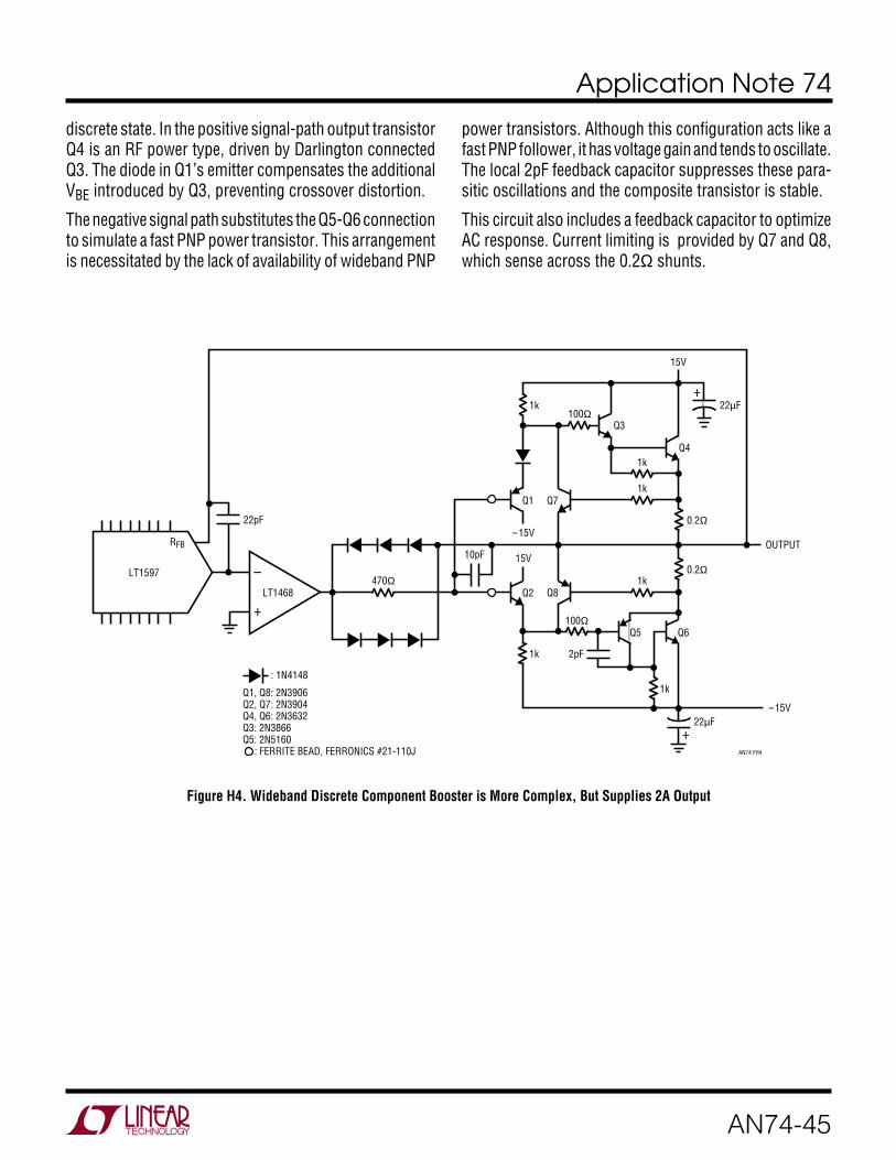
Application Note 74
AN74-45
discrete state. In the positive signal-path output transistorQ4 is an RF power type, driven by Darlington connectedQ3. The diode in Q1’s emitter compensates the additionalVBE introduced by Q3, preventing crossover distortion.
The negative signal path substitutes the Q5-Q6 connectionto simulate a fast PNP power transistor. This arrangementis necessitated by the lack of availability of wideband PNP
power transistors. Although this configuration acts like afast PNP follower, it has voltage gain and tends to oscillate.The local 2pF feedback capacitor suppresses these para-sitic oscillations and the composite transistor is stable.
This circuit also includes a feedback capacitor to optimizeAC response. Current limiting is provided by Q7 and Q8,which sense across the 0.2Ω shunts.
Figure H4. Wideband Discrete Component Booster is More Complex, But Supplies 2A Output
+
15V
–15V
–15V
15V
22µF
+22µF
Q3
1k
0.2Ω
0.2Ω
OUTPUT
1k
1k
100Ω
2pF
10pF
22pF
1k
100Ω
1k
1k470Ω
Q7Q1
Q5 Q6
Q8
AN74 FH4
Q2
Q4
RFB
LT1597–
+LT1468
: 1N4148
Q1, Q8: 2N3906 Q2, Q7: 2N3904 Q4, Q6: 2N3632 Q3: 2N3866 Q5: 2N5160 : FERRITE BEAD, FERRONICS #21-110J
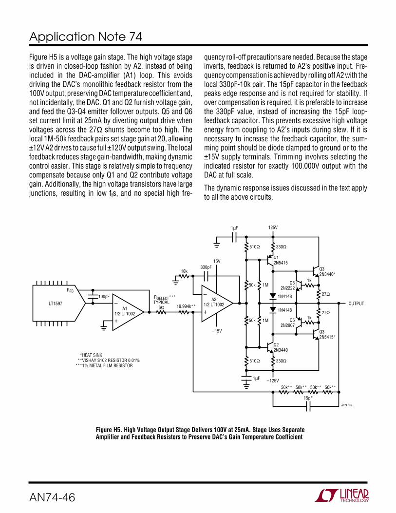
Application Note 74
AN74-46
Figure H5 is a voltage gain stage. The high voltage stageis driven in closed-loop fashion by A2, instead of beingincluded in the DAC-amplifier (A1) loop. This avoidsdriving the DAC’s monolithic feedback resistor from the100V output, preserving DAC temperature coefficient and,not incidentally, the DAC. Q1 and Q2 furnish voltage gain,and feed the Q3-Q4 emitter follower outputs. Q5 and Q6set current limit at 25mA by diverting output drive whenvoltages across the 27Ω shunts become too high. Thelocal 1M-50k feedback pairs set stage gain at 20, allowing±12V A2 drives to cause full ±120V output swing. The localfeedback reduces stage gain-bandwidth, making dynamiccontrol easier. This stage is relatively simple to frequencycompensate because only Q1 and Q2 contribute voltagegain. Additionally, the high voltage transistors have largejunctions, resulting in low fts, and no special high fre-
quency roll-off precautions are needed. Because the stageinverts, feedback is returned to A2’s positive input. Fre-quency compensation is achieved by rolling off A2 with thelocal 330pF-10k pair. The 15pF capacitor in the feedbackpeaks edge response and is not required for stability. Ifover compensation is required, it is preferable to increasethe 330pF value, instead of increasing the 15pF loop-feedback capacitor. This prevents excessive high voltageenergy from coupling to A2’s inputs during slew. If it isnecessary to increase the feedback capacitor, the sum-ming point should be diode clamped to ground or to the±15V supply terminals. Trimming involves selecting theindicated resistor for exactly 100.000V output with theDAC at full scale.
The dynamic response issues discussed in the text applyto all the above circuits.
Figure H5. High Voltage Output Stage Delivers 100V at 25mA. Stage Uses SeparateAmplifier and Feedback Resistors to Preserve DAC’s Gain Temperature Coefficient
–
+A2
1/2 LT1002
15V
–15V
330pF10k
19.994k**
RSELECT*** TYPICAL
6Ω
27Ω
OUTPUT
AN74 FH5
27Ω
330Ω510Ω
–125V1µF
15pF
1M50k
1M50k
330Ω510Ω
125V
1N4148
1N4148
1kQ5 2N2222
Q6 2N2907
Q3 2N3440*
Q1 2N5415
Q3 2N5415*
1k
50k**50k**50k**50k**
Q2 2N3440
1µF
RFB
LT1597–
+A1
1/2 LT1002
100pF
* **
***
HEAT SINK VISHAY S102 RESISTOR 0.01% 1% METAL FILM RESISTOR

Application Note 74
AN74-47Information furnished by Linear Technology Corporation is believed to be accurate and reliable.However, no responsibility is assumed for its use. Linear Technology Corporation makes no represen-tation that the interconnection of its circuits as described herein will not infringe on existing patent rights.
Figure H6 summarizes the booster stage’s characteristics.The IC-based stages offer simplicity while the complexdiscrete designs provide more output power.
VOLTAGE CURRENTFIGURE GAIN GAIN COMMENTS
H2 No Yes Simple 125mA Stage
H3 No Yes Simple 250mA/1.1A Stage
H4 No Yes Complex 2A Output
H5 Yes Minimal Complex ±120V Output
Figure H6. Summary of Booster Stage Characteristics

Application Note 74
AN74-48an74f LT/TP 0798 4K • PRINTED IN USA
LINEAR TECHNOLOGY CORPORATION 1998
Linear Technology Corporation1630 McCarthy Blvd., Milpitas, CA 95035-7417(408) 432-1900 FAX: (408) 434-0507 www.linear-tech.com