an4539 application note - home - stmicroelectronics · 1 getting the kitchen ready ... getting...
TRANSCRIPT

June 2014 DocID026506 Rev 1 1/33
AN4539Application note
HRTIM cookbook
Introduction
Among STM32 microcontrollers, STM32F334xx products have been developed to address market segments requiring digital signals with highly accurate timings, and especially digital power conversion applications. Among them:
• digital power supplies;
• lighting;
• uninterruptible Power Supplies;
• solar inverters;
• wireless chargers.
The STM32F334xx microcontrollers feature an High Resolution Timer (HRTIM) peripheral that can generate up to 10 signals and is able to handle a large variety of input signals for control, synchronization or protection purposes. Its modular architecture allows to address most of conversion topologies and multiple parallel converters, with the possibility to reconfigure them during run-time.
At first glance, reading the STM32F334 reference manual, this peripheral may appear complex, mostly because of the large control register set. To complement this extensive description, we have prepared an additional document that includes quick-start informations and a collection of examples.
In its first section, this cookbook aims to show that HRTIM programming is simple. The environment (the kitchen...) setup is first explained, followed by a number of simple examples given for understanding by practicing. These basic cases are provided to introduce step by step the timer features and to provide programming guidelines. This section should be read extensively by people not familiar with the HRTIM.
The second part is a collection of converter recipes to be used when starting a new design, either to pick up a ready-made code example, or to get ideas and programming tricks when dealing with a topology not described in this document. It shall be noted however that this cookbook does not cover the converter design itself (control techniques and components dimensioning) which may be described in dedicated application notes.
Each example is provided with a brief converter description when necessary (topology and connections to the MCU), the control waveform(s) and a code snippet. These snippets (and the equivalent code done based the STM32 HAL library) can be downloaded from www.st.com.
Table 1. Applicable products
Type Part numbers and product categories
Microcontrollers STM32F334xx
www.st.com

Contents AN4539
2/33 DocID026506 Rev 1
Contents
1 Getting the kitchen ready . . . . . . . . . . . . . . . . . . . . . . . . . . . . . . . . . . . . . 5
1.1 Prerequisites . . . . . . . . . . . . . . . . . . . . . . . . . . . . . . . . . . . . . . . . . . . . . . . 5
1.2 Hardware set-up . . . . . . . . . . . . . . . . . . . . . . . . . . . . . . . . . . . . . . . . . . . . . 5
1.3 Tools set-up . . . . . . . . . . . . . . . . . . . . . . . . . . . . . . . . . . . . . . . . . . . . . . . . 6
1.4 STM32F334 and HRTIM set-up . . . . . . . . . . . . . . . . . . . . . . . . . . . . . . . . . 6
1.4.1 System clock initialization . . . . . . . . . . . . . . . . . . . . . . . . . . . . . . . . . . . . 6
1.4.2 HRTIM initialization . . . . . . . . . . . . . . . . . . . . . . . . . . . . . . . . . . . . . . . . . 6
1.4.3 HRTIM DLL initialization . . . . . . . . . . . . . . . . . . . . . . . . . . . . . . . . . . . . . 7
1.4.4 HRTIM I/Os initialization . . . . . . . . . . . . . . . . . . . . . . . . . . . . . . . . . . . . . 7
1.4.5 Other peripherals initialization . . . . . . . . . . . . . . . . . . . . . . . . . . . . . . . . . 7
1.4.6 HRTIM functionality check . . . . . . . . . . . . . . . . . . . . . . . . . . . . . . . . . . . . 8
2 HRTIM operating principles basics . . . . . . . . . . . . . . . . . . . . . . . . . . . . 10
2.1 Single PWM generation . . . . . . . . . . . . . . . . . . . . . . . . . . . . . . . . . . . . . . 10
2.2 Generating multiple PWMs . . . . . . . . . . . . . . . . . . . . . . . . . . . . . . . . . . . . 12
2.3 Generating PWM with other timing units and the master timer . . . . . . . . 15
2.4 Arbitrary waveform generation . . . . . . . . . . . . . . . . . . . . . . . . . . . . . . . . . 17
3 Voltage mode dual buck converter . . . . . . . . . . . . . . . . . . . . . . . . . . . . 19
4 Voltage mode buck converter with synchronous rectification and fault protection . . . . . . . . . . . . . . . . . . . . . . . . . . . . . . 22
5 Non-inverting buck-boost converter . . . . . . . . . . . . . . . . . . . . . . . . . . . 24
6 Transition mode power factor controller . . . . . . . . . . . . . . . . . . . . . . . 27
7 Other examples . . . . . . . . . . . . . . . . . . . . . . . . . . . . . . . . . . . . . . . . . . . . 31
8 Revision history . . . . . . . . . . . . . . . . . . . . . . . . . . . . . . . . . . . . . . . . . . . 32
DocID026506 Rev 1 3/33
AN4539 List of tables
3
List of tables
Table 1. Applicable products . . . . . . . . . . . . . . . . . . . . . . . . . . . . . . . . . . . . . . . . . . . . . . . . . . . . . . . 1Table 2. Timer resolution and min PWM frequency for fHRTIM = 144 MHz. . . . . . . . . . . . . . . . . . . 13Table 3. Document revision history . . . . . . . . . . . . . . . . . . . . . . . . . . . . . . . . . . . . . . . . . . . . . . . . . 32

List of figures AN4539
4/33 DocID026506 Rev 1
List of figures
Figure 1. Basic PWM generation . . . . . . . . . . . . . . . . . . . . . . . . . . . . . . . . . . . . . . . . . . . . . . . . . . . . 11Figure 2. HRTIM configuration for generating basic PWM signals . . . . . . . . . . . . . . . . . . . . . . . . . . 12Figure 3. Generation of multiple PWM signals. . . . . . . . . . . . . . . . . . . . . . . . . . . . . . . . . . . . . . . . . . 14Figure 4. PWM generation with the master timer. . . . . . . . . . . . . . . . . . . . . . . . . . . . . . . . . . . . . . . . 16Figure 5. Arbitrary waveform generation . . . . . . . . . . . . . . . . . . . . . . . . . . . . . . . . . . . . . . . . . . . . . . 17Figure 6. Voltage-mode buck converter . . . . . . . . . . . . . . . . . . . . . . . . . . . . . . . . . . . . . . . . . . . . . . . 19Figure 7. VM buck waveforms, including ADC sampling and interrupts . . . . . . . . . . . . . . . . . . . . . . 20Figure 8. PWM interrupts and register update . . . . . . . . . . . . . . . . . . . . . . . . . . . . . . . . . . . . . . . . . . 20Figure 9. Voltage mode buck with synchronous rectification . . . . . . . . . . . . . . . . . . . . . . . . . . . . . . . 22Figure 10. Buck operation with FAULT . . . . . . . . . . . . . . . . . . . . . . . . . . . . . . . . . . . . . . . . . . . . . . . . 23Figure 11. Non-inverting buck-boost converter . . . . . . . . . . . . . . . . . . . . . . . . . . . . . . . . . . . . . . . . . . 24Figure 12. Buck-boost operating mode . . . . . . . . . . . . . . . . . . . . . . . . . . . . . . . . . . . . . . . . . . . . . . . . 25Figure 13. Buck-boost converter operating waveforms . . . . . . . . . . . . . . . . . . . . . . . . . . . . . . . . . . . . 25Figure 14. Transition mode PFC . . . . . . . . . . . . . . . . . . . . . . . . . . . . . . . . . . . . . . . . . . . . . . . . . . . . . 27Figure 15. Transition mode PFC operation at Ton max and during over-current. . . . . . . . . . . . . . . . . 28Figure 16. Transition mode PFC operation at Toff max and Toff min . . . . . . . . . . . . . . . . . . . . . . . . . 29

DocID026506 Rev 1 5/33
AN4539 Getting the kitchen ready
32
1 Getting the kitchen ready
In this section, we’ll make sure to have all the necessary ingredients ready before starting, so that we can concentrate on the HRTIM programming only.
The following documents are to be considered as reference:
• STM32F334x4/x6/x8 Datasheet
• STM32F334x4/x6/x8 Errata sheet
• RM0364 Reference manual STM32F334xx advanced ARM®-based 32-bit MCUs
• UM1733: Getting Started with STM32F334 Discovery Kit
• UM1735: Discovery kit for STM32F3 series - with STM32F334C8 MCU
• UM1736: Getting started with STM32F334 Discovery software development tools
• AN4885: High brightness LED dimming using the STM32F3348 Discovery
A preliminary reading of the HRTIM chapter in the RM0364 will be useful.
1.1 Prerequisites
Before enjoying the flavors of the HRTIM, let’s list the prerequisites. It is expected from the reader basic C programming skills and minimal experience on MCUs and development environments, as well as a theoretical background on switched mode power supplies. Control strategies and components dimensioning details are exceeding the scope of this application note, they are available in a vast literature.
For the sake of simplicity, this cookbook only considers logic signals or analog voltages conditioned to be directly handled by the MCU, so as to be voltage level agnostic. However some references are made to external components interfacing and side effects from power switchings, whenever the timer or MCU has some features to handle them.
Last, it is reminded that it is required to have power applications operated by skilled technical personnel to avoid risks of electrical shocks, burns or even death, should the STM32F334 and the HRTIM may be used in applications with hazardous voltage levels.
1.2 Hardware set-up
The STM32F334 Discovery board is a very affordable tool and is the best option to start (and go on) experimenting with the HRTIM (order code: STM32F3348-DISCO). It includes the programming interface and a USB cable is the only necessary additional material to have the chip programmed and debugged. All I/Os are made available on 2.54 mm spaced pins so that it can also be connected to a perfboard / stripboard / breadboard. The kit also features two power converters: an inverted buck for LED drive and a low-voltage buck/boost converter with independent inputs and outputs.
An oscilloscope is mandatory, eventually coupled with a logic analyzer for the configurations where more than 4 channels must be monitored. To visualize the subtle high-resolution steps, the oscilloscope has to have a sampling rate above 1GS/s at least with an option to have interleaved acquisition so as to increase the timing accuracy above the 217ps timer resolution.

Getting the kitchen ready AN4539
6/33 DocID026506 Rev 1
One or several function generator are also of great help to emulate the feedbacks from the power converter (either logic pulses or analog signals) during the early debugging phases. The generator must have a trigger input for some specific cases. If missing, it is also possible to have the feedback signal emulated by the HRTIM itself using free timing units, with some more coding effort (or software example reuse).
1.3 Tools set-up
It is necessary to have a compiler installed (all demos are fitting within 32K), as well as an IDE supporting the ST-LINK-V2 debug interface.
The code snippets given below are compiler agnostic. They shall simply be copied into a generic HRTIM project template for any kind of toolchain.
The software sources are delivered with workspaces for the following toolchains:
• IAR (EWARM 7.10.3);
• KEIL® (MDK-ARM 4.7).
1.4 STM32F334 and HRTIM set-up
1.4.1 System clock initialization
The HRTIM needs to be feeded directly by the PLL high-frequency output to provide the high-resolution. Two options are available:
• the crystal-based High-Speed External (HSE) oscillator, providing 144MHz when multiplied by the PLL. In this case, the high-resolution is 217ps (1/32 of a 144MHz clock period);
• the High-Speed Internal (HSI) oscillator, able to provide 128MHz (8MHz multiplied by 16 by the PLL). In this case, the high-resolution step is 244ps (1/32 of a 128MHz clock period). The option is available for a limited temperature range, see the STM32F334 datasheet for conditions.
Clock initialization is done in the main routine using the SystemClock_Config() function right after the HAL libray initialisation (HAL_Init).
The CPU clock is also derived from the PLL, after a division by 2, so that it can be up to half of the PLL output frequency (72MHz with HSE and 64MHz with HSI). It can also be reduced to decrease MCU consumption while keeping the high-resolution functional.
The SystemCoreClockUpdate function can eventually be executed in the main to verify the CPU operating frequency: the frequency is updated in the SystemCoreClock variable.
1.4.2 HRTIM initialization
This section details step by step how the HRTIM is initialized, including individual function calls. Practically, this is done within the HAL_HRTIM_Init and HAL_HRTIM_MspInit routines.
HRTIM clock initialization
Once the MCU is up and running, the HRTIM must be clocked before being programmed. This is done using the Reset and Clock controller (RCC), in 2 steps:

DocID026506 Rev 1 7/33
AN4539 Getting the kitchen ready
32
1. Selection of the high-speed PLL output for the HRTIM in RCC_CFGR3 register:
__HAL_RCC_HRTIM1_CONFIG(RCC_HRTIM1CLK_PLLCLK);
2. Clock enable for the registers mapped on the APB2 bus.
__HRTIM1_CLK_ENABLE();
1.4.3 HRTIM DLL initialization
The HRTIM’s Delay-Locked Loop (DLL) is responsible for providing fine-grained timings and divide the high-frequency (144 or 128MHz) clock period into 32 evenly spaced steps.
This DLL must be calibrated at least once before high-resolution can be used. The calibration can be transparently re-launched by software during HRTIM operation if voltage or temperature conditions have changed. It is also possible to enable periodic calibration by hardware.
The code snippet below shows how the calibration is done. The high-resolution can be used once the DLLRDY flag has been set.
/* DLL calibration: periodic calibration enabled, period set to 14µs */
HRTIM1->sCommonRegs.DLLCR = HRTIM_CALIBRATIONRATE_14| HRTIM_DLLCR_CALEN;
/* Check DLL end of calibration flag */
while(HRTIM1->sCommonRegs.ISR & HRTIM_IT_DLLRDY == RESET);
It is recommended to have the periodic calibration enabled, with the lowest calibration period (set at 14µs), as default condition.
Note: The code here below will cause the execution to stall if the DLL does not lock (typically if the HSE oscillator is not properly configured). The HAL library includes a function to perform the calibration which has a timeout verification and redirect in an error handler if necessary. This function is the one used in the HAL-based software example.
1.4.4 HRTIM I/Os initialization
The HRTIM inputs and outputs are mapped on standard I/O ports and have to be programmed as any other I/O peripheral. The HRTIM alternate functions are split between:
• AF13 channel (for HRTIM I/O ports located on ports A and B);
• AF3 channel (for HRTIM I/O ports located on port C)
The HRTIM I/Os initialization must be done in two phases. The HRTIM inputs are initialized first, prior to the HRTIM registers, in the HAL_HRTIM_MspInit function.
The HRTIM outputs must be initialized after the HRTIM control registers programming (done in the GPIO_HRTIM_outputs_Config function in the examples), and once the counters are enabled. This is to ensure that the outputs states are correctly defined inside the HRTIM before passing the control from the GPIO circuitry to the HRTIM timer.
1.4.5 Other peripherals initialization
The HRTIM interacts with many of the MCU peripherals, as listed below. It is not mandatory to have all of them initialized to have the HRTIM operating. Initialization codes for the peripherals below are available in some of the examples described later.

Getting the kitchen ready AN4539
8/33 DocID026506 Rev 1
Nested Vectored Interrupt Controller (NVIC)
The HRTIM interrupts requests are grouped onto 7 interrupts vectors. All faults are grouped within a distinct vector that can be set with a very high priority.
The NVIC’s part related to the HRTIM is programmed in the HAL_HRTIM_MspInit function.
DMA controller
Most of interrupt requests can be used as DMA requests and are grouped on 6 DMA channels (one per timing unit including the master timer).
DMA-based HRTIM operation is enabled when starting the timer, with specific start/stop function such as HAL_HRTIM_WaveformCounterStart_DMA.
Refer to Section 2: HRTIM operating principles basics for more details.
Comparators
Three built-in comparators can be used to condition analog signals: they must be initialized before the output is routed to the HRTIM.
The initialization includes the analog inputs programming, clock enable and polarity.
Operational amplifier
The built-in operational amplifier can amplify low voltage signals to be routed to the ADC or to the comparators, and also directly act as a comparator (with lower speed compared with the regular ones). It must be initialized similarly to the comparator.
ADC converters
The HRTIM can trigger any of the two ADC converters. They shall be initialized to receive external triggers, on their regular and/or injected sequencers.
Another possible use of ADCs consists in using the analog watchdog to trigger external events on the HRTIM (for output set/reset or counter reset purposes).
DAC converters
The DAC converters are mostly used to define the comparator’s thresholds. They can be updated synchronously with HRTIM operation by means of HRTIM’s DAC triggers.
General purpose timers
The HRTIM can also be linked with other on-chip timers for the following use:
• as external events;
• as burst mode trigger or clock;
• for HRTIM registers update triggering.
1.4.6 HRTIM functionality check
Once the whole initialization is completed, it’s possible to verify that the HRTIM is ready to go with the simple code below. This example code (HRTIM_BasicPWM example) enables the HRTIM TD1 output and toggles it by software.
/* Use the PLLx2 clock for HRTIM */
__HAL_RCC_HRTIM1_CONFIG(RCC_HRTIM1CLK_PLLCLK);

DocID026506 Rev 1 9/33
AN4539 Getting the kitchen ready
32
/* Enable HRTIM clock*/
__HRTIM1_CLK_ENABLE();
/* DLL calibration: periodic calibration enabled, period set to 14µs */
HRTIM1->sCommonRegs.DLLCR = HRTIM_CALIBRATIONRATE_14| HRTIM_DLLCR_CALEN;
/* Check DLL end of calibration flag */
while(HRTIM1->sCommonRegs.ISR & HRTIM_IT_DLLRDY == RESET);
HRTIM1->sCommonRegs.OENR = HRTIM_OENR_TD1OEN; /* Enable TD1 output */
GPIO_HRTIM_outputs_Config(); /* Initialize HRTIM outputs */
while(1)
{
/* Set and reset TD1 by software */
HRTIM1->sTimerxRegs[HRTIM_TIMERINDEX_TIMER_D].SETx1R = HRTIM_SET1R_SST;
HRTIM1->sTimerxRegs[HRTIM_TIMERINDEX_TIMER_D].RSTx1R = HRTIM_RST1R_SRT;
}
The snippet reproduced here is available in the HRTIM_Snippets and HRTIM_BasicPWM examples. In both cases the example must be selected with the #define HRTIM_CHECK statement.
For the remaining part of this document, the clock and DLL initialization part will not be repeated, it will be replaced by a call to the HRTIM_Minimal_Config() function.

HRTIM operating principles basics AN4539
10/33 DocID026506 Rev 1
2 HRTIM operating principles basics
Despite an apparent complexity due to the number of features and to its modular architecture, the HRTIM is basically made of six 16-bit auto-reload up-counters with 4 compare registers each.
Period and compare programming
The high-resolution programming is made completely transparent, so as to have the look-and-feel of a timer clocked by a 4.6 GHz clock (144MHz x 32), when using the HSE oscillators. The timings (period and compare) can be directly written into a unique 16-bit register with high-resolution accuracy. A counting period will simply be programmed using the formula:
PERTcounting
THigh res–--------------------------=
For instance, a 10µs time period is obtained by setting the period register to 10µs / 217ps = 46082d and is programmed as follows:
HRTIM1->sTimerxRegs[HRTIM_TIMERINDEX_TIMER_D].PERxR = 0x0000B400;
Should the result exceed the 16-bit range, the high-resolution can be adjusted by multiples of 217 ps, so as to be have the period value within the 16-bit range.
Set/reset crossbar
Each timing unit holds the control of 2 outputs via a set/reset crossbar. Compared to usual frozen PWM modes where the output is set at the beginning of the counting period and reset on a given compare match, the crossbar offers much more flexibility in defining how an ouput is set or reset. It gives the possibility to have any of timer events setting or resetting an output.
Output stage
The waveform generated by the set / reset crossbar is finally passed through an output stage for “post-processing” such as
• generating complementary signal with a deadtime;
• adding high-frequency modulation;
• modifying the signal polarity;
• shutting down the output for protection purpose.
With this few features in mind, it is now possible to elaborate the first elemental PWM signals.
2.1 Single PWM generation
In this section we will discuss:
• Timer continuous mode;
• Simplest crossbar configuration;
• Output stage enable.

DocID026506 Rev 1 11/33
AN4539 HRTIM operating principles basics
32
PWM signals are the elemental bricks of most power converter and are used for many other purposes such as driving electric motors, piezo buzzers or emulating DAC converters.
This example shows that this can be achieved very simply with the HRTIM by programming a limited number of HRTIM registers.
Let’s consider a 100kHz PWM signal with 50% duty cycle to be generated on TA1 output, as exemplified in Figure 1.
Figure 1. Basic PWM generation
The timer D must be configured in continuous (free-running) mode. The PWM period is programmed in the period register HRTIM_PERAR using the formula .
PERfHRCK
fPWM----------------=
Here (144MHz x 32)/100kHz = 46080d (0xB400).
The 50% duty cycle is obtained by multiplying the period by the duty cycle: PER x DC.
Here 0.5 x 46080d = 23040d (0x5A00).
The waveform is elaborated in the set/reset crossbar with the registers HRTIM_SETx1R (PER bit set) and HRTIM_RSTx1R (CMP1 bit set).
Finally, the output is enabled with the HRTIM_OENR register.
The sequence just described gives an overview of the timer features involved in a simple PWM generation. The configuration is schematized in Figure 2.

HRTIM operating principles basics AN4539
12/33 DocID026506 Rev 1
Figure 2. HRTIM configuration for generating basic PWM signals
The example code is provided in the HRTIM_BasicPWM example, and the snippet reproduced below is available in the HRTIM_Snippets example. In both cases the example must be selected with the #define SINGLE_PWM statement.
/* TIMD counter operating in continuous mode */
HRTIM1->sTimerxRegs[HRTIM_TIMERINDEX_TIMER_D].TIMxCR = HRTIM_TIMCR_CONT;
/* Set period to 100kHz and duty cycle (CMP1) to 50% */
HRTIM1->sTimerxRegs[HRTIM_TIMERINDEX_TIMER_D].PERxR = 0x0000B400;
HRTIM1->sTimerxRegs[HRTIM_TIMERINDEX_TIMER_D].CMP1xR = 0x00005A00;
/* TD1 output set on TIMD period and reset on TIMD CMP1 event*/
HRTIM1->sTimerxRegs[HRTIM_TIMERINDEX_TIMER_D].SETx1R = HRTIM_SET1R_PER;
HRTIM1->sTimerxRegs[HRTIM_TIMERINDEX_TIMER_D].RSTx1R = HRTIM_RST1R_CMP1;
HRTIM1->sMasterRegs.MCR = HRTIM_MCR_TDCEN; /* Start Timer D */
HRTIM1->sCommonRegs.OENR = HRTIM_OENR_TD1OEN; /* Enable TD1 output */
GPIO_HRTIM_outputs_Config(); /* Initialize HRTIM GPIO outputs */
2.2 Generating multiple PWMs
In this section we will discuss:
• multiple timing unit usage;
• register preload.
The HRTIM is able to generate up to 10 PWM signals with 5 independent frequencies (or 6 frequencies when the master timer is used, see Section 2.3: Generating PWM with other timing units and the master timer).
In the example below, 4 PWM signals with 2 different timebases are generated.
The Timer D generates two phase-shifted 100kHz with 25% duty cycle on TD1 and TD2, with the following conditions:
• TD1: Set on TD Period, reset on TD CMP1;
• TD2: Set on TD CMP2, reset on TD Period.

DocID026506 Rev 1 13/33
AN4539 HRTIM operating principles basics
32
The Timer A generates two phase-shifted 33.333kHz PWMs with 25% duty cycle on TA1 and TA2, with the following conditions:
• TA1: Set on TA Period, reset on TA CMP1
• TA2: Set on TA CMP2, reset on TA CMP3
The timer A period is below the minimum frequency available at the highest resolution, as shown in Table 2:
In this case, the frequency prescaler must be set to 4 and the period calculated as following: PER = fHRCK / fPWM. Here, a frequency of 33.333 kHz is obtained by setting PER register to (144MHz * 8) / 33.333kHz) = 34560d (0x8700).
Even though the duty cycle is not updated in this example, and to be close to a practical use case, the register preload mechanism is enabled with the PREEN bit. The REP (repetition) event triggers the transfer of the preload registers on each and every period beginning.
Note: A delay can be noticed at the PWM start-up, between TA1/TA2 and TD1/TD2 waveform. This delay is normal and due to the fact that the 1st update event (causing compare registers to take their programmed value) occurs only after the 1st counting period is elapsed. Should the waveforms be started without this delay, it is possible to force a register update by software (using TASWU and TDSWU bits) to have all active compare registers contents updated at once.
Table 2. Timer resolution and min PWM frequency for fHRTIM = 144 MHz
CKPSC[2:0]Prescaling
ratiofHRCK
equivalent frequencyResolution
MinimumPWM frequency
000 1 144x32 MHz = 4.608 GHz 217 ps 70.3 kHz
001 2 144x16 MHz = 2.304 GHz 434 ps 35.1 kHz
010 4 144x8 MHz = 1.152 GHz 868 ps 17.6 kHz
011 8 144x4 MHz = 576 MHz 1.73 ns 8.8 kHz
100 16 144x2 MHz = 288 MHz 3.47 ns 4.4 kHz
101 32 144MHz 6.95 ns 2.2 kHz
110 64 144/2 MHz = 72 MHz 13.88 ns 1.1 kHz
111 128 144/4 MHz = 36 MHz 27.7 ns 550 Hz

HRTIM operating principles basics AN4539
14/33 DocID026506 Rev 1
Figure 3. Generation of multiple PWM signals
The example code is provided in the HRTIM_BasicPWM example, and the snippet reproduced here-below is available in the HRTIM_Snippets example. In both cases the example must be selected with the #define MULTIPLE_PWM statement.
/* --------------------- Timer D initialization ------------------------ */
/* TIMD counter operating in continuous mode, preload enabled on REP event */
HRTIM1->sTimerxRegs[HRTIM_TIMERINDEX_TIMER_D].TIMxCR =
HRTIM_TIMCR_CONT + HRTIM_TIMCR_PREEN + HRTIM_TIMCR_TREPU;
/* Set period to 100kHz, CMP1 to 25% and CMP2 to 75% of period */
HRTIM1->sTimerxRegs[HRTIM_TIMERINDEX_TIMER_D].PERxR = _100KHz_PERIOD;
HRTIM1->sTimerxRegs[HRTIM_TIMERINDEX_TIMER_D].CMP1xR = _100KHz_PERIOD/4;
HRTIM1->sTimerxRegs[HRTIM_TIMERINDEX_TIMER_D].CMP2xR = (3*_100KHz_PERIOD)/4;
/* TD1 output set on TIMD period and reset on TIMD CMP1 event*/
HRTIM1->sTimerxRegs[HRTIM_TIMERINDEX_TIMER_D].SETx1R = HRTIM_SET1R_PER;
HRTIM1->sTimerxRegs[HRTIM_TIMERINDEX_TIMER_D].RSTx1R = HRTIM_RST1R_CMP1;
/* TD2 output set on TIMD CMP2 and reset on TIMD period event*/
HRTIM1->sTimerxRegs[HRTIM_TIMERINDEX_TIMER_D].SETx2R = HRTIM_SET2R_CMP2;
HRTIM1->sTimerxRegs[HRTIM_TIMERINDEX_TIMER_D].RSTx2R = HRTIM_RST2R_PER;

DocID026506 Rev 1 15/33
AN4539 HRTIM operating principles basics
32
/* --------------------- Timer A initialization ---------------------- */
/* TIMA counter operating in continuous mode with prescaler = 010b (div. by 4) */
/* Preload enabled on REP event*/
HRTIM1->sTimerxRegs[HRTIM_TIMERINDEX_TIMER_A].TIMxCR = HRTIM_TIMCR_CONT
+ HRTIM_TIMCR_PREEN + HRTIM_TIMCR_TREPU + HRTIM_TIMCR_CK_PSC_1;
/* Set period to 33kHz and duty cycles to 25% */
HRTIM1->sTimerxRegs[HRTIM_TIMERINDEX_TIMER_A].PERxR = _33KHz_PERIOD;
HRTIM1->sTimerxRegs[HRTIM_TIMERINDEX_TIMER_A].CMP1xR = _33KHz_PERIOD/4;
HRTIM1->sTimerxRegs[HRTIM_TIMERINDEX_TIMER_A].CMP2xR = _33KHz_PERIOD/2;
HRTIM1->sTimerxRegs[HRTIM_TIMERINDEX_TIMER_A].CMP3xR = (3*_33KHz_PERIOD)/4;
/* TA1 output set on TIMA period and reset on TIMA CMP1 event*/
HRTIM1->sTimerxRegs[HRTIM_TIMERINDEX_TIMER_A].SETx1R = HRTIM_SET1R_PER;
HRTIM1->sTimerxRegs[HRTIM_TIMERINDEX_TIMER_A].RSTx1R = HRTIM_RST1R_CMP1;
/* TA2 output set on TIMA CMP2 and reset on TIMA period event*/
HRTIM1->sTimerxRegs[HRTIM_TIMERINDEX_TIMER_A].SETx2R = HRTIM_SET2R_CMP2;
HRTIM1->sTimerxRegs[HRTIM_TIMERINDEX_TIMER_A].RSTx2R = HRTIM_RST2R_CMP3;
/* Enable TA1, TA2, TD1 and TD2 outputs */
HRTIM1->sCommonRegs.OENR = HRTIM_OENR_TA1OEN + HRTIM_OENR_TA2OEN +
HRTIM_OENR_TD1OEN + HRTIM_OENR_TD2OEN;
GPIO_HRTIM_outputs_Config(); /* Initialize HRTIM GPIO outputs */
/* Start Timer A and Timer D */
HRTIM1->sMasterRegs.MCR = HRTIM_MCR_TACEN + HRTIM_MCR_TDCEN;
2.3 Generating PWM with other timing units and the master timer
In this section we will discuss:
• Generation of signals on outputs not related to a given timer.
This example shows that thanks to the set/reset crossbar, it’s possible to have PWM signals (or other waveforms) generated on a given output with any other available timer. This is interesting in the following cases:
• to generate a 6th PWM independent frequency with the master timer, as in the example below;
• to work-around pin-out constraints, for instance using Timer E to generate waveforms even if TE1 and TE2 outputs are not available (typically on small pin-count package).
Note: It is mandatory to have the same prescaling factors for all timer sharing resources (for instance master timer and timer A must have identical CKPSC[2:0] values if master timer is controlling TA1 or TA2 outputs).

HRTIM operating principles basics AN4539
16/33 DocID026506 Rev 1
In the example below, 2 PWM signals with slightly different switching frequencies are generated on TD1 and TD2 outputs, with the following conditions:
• TD1: Set on TD Period, reset on TD CMP1;
• TD2: Set on Master Period, reset on Master CMP1.
The frequencies are set to slightly different values to ease visualization on oscilloscope (the signals have a relatively slow phase-shift variation), and to demonstrate that the signals are completely asynchronous.
Figure 4. PWM generation with the master timer
The provided code is the HRTIM_BasicPWM example, and the snippet reproduced below is available in the HRTIM_Snippets example. In both cases the example must be selected with the #define PWM_MASTER statement.
/* --------------------- Master Timer initialization ------------------- */
/* Master counter operating in continuous mode, Preload enabled on REP event*/
HRTIM1->sMasterRegs.MCR = HRTIM_MCR_CONT + HRTIM_MCR_PREEN + HRTIM_MCR_MREPU;
/* Set period to 101kHz and duty cycle to 50% */
HRTIM1->sMasterRegs.MPER = _100KHz_Plus_PERIOD;
HRTIM1->sMasterRegs.MCMP1R = _100KHz_Plus_PERIOD/2;
/* --------------------- Timer D initialization ------------------------ */
/* TIMD counter operating in continuous mode, preload enabled on REP event */
HRTIM1->sTimerxRegs[HRTIM_TIMERINDEX_TIMER_D].TIMxCR =
HRTIM_TIMCR_CONT + HRTIM_TIMCR_PREEN + HRTIM_TIMCR_TREPU;
/* Set period to 100kHz and duty cycle (CMP1) to 50% */
HRTIM1->sTimerxRegs[HRTIM_TIMERINDEX_TIMER_D].PERxR = _100KHz_PERIOD;

DocID026506 Rev 1 17/33
AN4539 HRTIM operating principles basics
32
HRTIM1->sTimerxRegs[HRTIM_TIMERINDEX_TIMER_D].CMP1xR = _100KHz_PERIOD/4;
/* TD1 output set on TIMD period and reset on TIMD CMP1 event*/
HRTIM1->sTimerxRegs[HRTIM_TIMERINDEX_TIMER_D].SETx1R = HRTIM_SET1R_PER;
HRTIM1->sTimerxRegs[HRTIM_TIMERINDEX_TIMER_D].RSTx1R = HRTIM_RST1R_CMP1;
/* TD2 output set on TIMD CMP2 and reset on TIMD period event*/
HRTIM1->sTimerxRegs[HRTIM_TIMERINDEX_TIMER_D].SETx2R = HRTIM_SET2R_MSTPER;
HRTIM1->sTimerxRegs[HRTIM_TIMERINDEX_TIMER_D].RSTx2R = HRTIM_RST2R_MSTCMP1;
/* Enable TD1 and TD2 outputs */
HRTIM1->sCommonRegs.OENR = HRTIM_OENR_TD1OEN + HRTIM_OENR_TD2OEN;
GPIO_HRTIM_outputs_Config(); /* Initialize HRTIM GPIO outputs */
/* Start Master Timer and Timer D */
HRTIM1->sMasterRegs.MCR |= HRTIM_MCR_MCEN + HRTIM_MCR_TDCEN;
2.4 Arbitrary waveform generation
In this section we will discuss:
• Waveforms with multiple set/reset/toggle requests per period.
This example shows that waveforms other than PWMs can very easily be generated thanks to the 32 concurrent set/reset sources of the crossbar.
In the example below, 2 arbitrary waveforms are generated on TD1 and TD2 outputs, with the following conditions:
• TD1: Toggle on TD Period, toggle on TD CMP1, toggle on TD CMP2;
• TD2: Set on TD Period and TD CMP3, reset on TD CMP2 and TD CMP3.
Figure 5. Arbitrary waveform generation

HRTIM operating principles basics AN4539
18/33 DocID026506 Rev 1
The provided code is the HRTIM_BasicPWM example, and the snippet reproduced below is available in the HRTIM_Snippets example. In both cases the example must be selected with the #define ARBITRARY_WAVEFORM statement.
/* --------------------- Timer D initialization ------------------------ */
/* TIMD counter operating in continuous mode, preload enabled on REP event */
HRTIM1->sTimerxRegs[HRTIM_TIMERINDEX_TIMER_D].TIMxCR = HRTIM_TIMCR_CONT
+ HRTIM_TIMCR_PREEN + HRTIM_TIMCR_TREPU;
/* Set period to 100kHz and edge timings */
HRTIM1->sTimerxRegs[HRTIM_TIMERINDEX_TIMER_D].PERxR = _100KHz_PERIOD;
HRTIM1->sTimerxRegs[HRTIM_TIMERINDEX_TIMER_D].CMP1xR = _100KHz_PERIOD/4;
HRTIM1->sTimerxRegs[HRTIM_TIMERINDEX_TIMER_D].CMP2xR = (3*_100KHz_PERIOD)/8;
HRTIM1->sTimerxRegs[HRTIM_TIMERINDEX_TIMER_D].CMP3xR = _100KHz_PERIOD/2;
/* TD1 toggles on TIMD period, CMP1 and CMP2 event*/
HRTIM1->sTimerxRegs[HRTIM_TIMERINDEX_TIMER_D].SETx1R = HRTIM_SET1R_PER + HRTIM_SET1R_CMP1 + HRTIM_SET1R_CMP2;
HRTIM1->sTimerxRegs[HRTIM_TIMERINDEX_TIMER_D].RSTx1R = HRTIM_RST1R_PER + HRTIM_RST1R_CMP1 + HRTIM_RST1R_CMP2;
/* TD2 output set on TIMD PER and CMP2 and reset on TIMD CMP1 and CMP3 event*/
HRTIM1->sTimerxRegs[HRTIM_TIMERINDEX_TIMER_D].SETx2R = HRTIM_SET2R_PER + HRTIM_SET2R_CMP2;
HRTIM1->sTimerxRegs[HRTIM_TIMERINDEX_TIMER_D].RSTx2R = HRTIM_RST2R_CMP1 + HRTIM_RST2R_CMP3;
/* Enable TD1 and TD2 outputs */
HRTIM1->sCommonRegs.OENR = HRTIM_OENR_TD1OEN + HRTIM_OENR_TD2OEN;
GPIO_HRTIM_outputs_Config(); /* Initialize HRTIM GPIO outputs */
/* Start Timer D */
HRTIM1->sMasterRegs.MCR = HRTIM_MCR_TDCEN;
DocID026506 Rev 1 19/33
AN4539 Voltage mode dual buck converter
32
3 Voltage mode dual buck converter
In this section we will discuss:
• Repetition counter interrupts;
• ADC trigger;
• Register update on repetition event.
Buck converters are mostly used to perform step-down voltage conversions. They are usually operating at fixed frequency and variable duty cycle. In the ideal converter, the Vin/Vout ratio depends only upon the duty cycle D applied to the power switch:
Vout D V× in=
Practically, the duty cycle is adjusted by the control algorithm to maintain the desired output voltage. In this example, the voltage mode buck converter is considered: the duty cycle is controlled based on the converter output voltage reading. An input voltage reading can eventually be added to implement a feed-forward compensation.
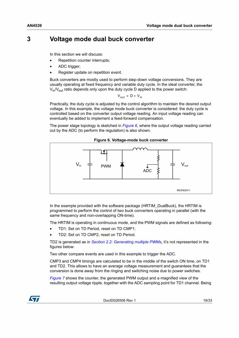
The power stage topology is sketched in Figure 6, where the output voltage reading carried out by the ADC (to perform the regulation) is also shown.
Figure 6. Voltage-mode buck converter
In the example provided with the software package (HRTIM_DualBuck), the HRTIM is programmed to perform the control of two buck converters operating in parallel (with the same frequency and non-overlapping ON-time).
The HRTIM is operating in continuous mode, and the PWM signals are defined as following:
• TD1: Set on TD Period, reset on TD CMP1;
• TD2: Set on TD CMP2, reset on TD Period.
TD2 is generated as in Section 2.2: Generating multiple PWMs, it’s not represented in the figures below.
Two other compare events are used in this example to trigger the ADC.
CMP3 and CMP4 timings are calculated to be in the middle of the switch ON time, on TD1 and TD2. This allows to have an average voltage measurement and guarantees that the conversion is done away from the ringing and switching noise due to power switches.
Figure 7 shows the counter, the generated PWM output and a magnified view of the resulting output voltage ripple, together with the ADC sampling point for TD1 channel. Being

Voltage mode dual buck converter AN4539
20/33 DocID026506 Rev 1
given the high PWM frequency, the repetition counter is used to decrease the number of interrupts service routines. In Figure 7 the repetition autoreload rate is set to 1, so that the ISR rate is half the PWM frequency. In the example, the repetition rate is set to 127 to have a very low change rate.
Figure 7. VM buck waveforms, including ADC sampling and interrupts
Figure 8 shows how the duty cycle is updated, once the duty cycle on TD1 has been completed in the interrupt routine. The timer is programmed to have a register update occurring on each repetition event.
Figure 8. PWM interrupts and register update
Dual buck demo overview
The duty cycle on TD1 is continuously varied in an interrupt service routine generated on repetition event, to mimic a real converter management. A low-pass filtered signal reflecting the PWM duty cycle can be monitored on STM32F334 discovery kit TP3 test point.

DocID026506 Rev 1 21/33
AN4539 Voltage mode dual buck converter
32
The duty cycle on TD2 is constant.
The ADC is configured to have conversions triggered in the middle of the ON time of each output. The 2 conversions are done with the same ADC injected trigger (this is possible since the 2 signals are not overlapping). The ADC is programmed in discontinuous injected mode (1 conversion triggered on CMP3, another on CMP4).
The 2 conversions are done on the same input (PA4): TD1’s low-pass filtered PWM can be connected to PA4 for monitoring ADC conversions with the debugger. For a real use case, it is easy to reprogram the ADC to have the conversions done on each buck output voltage.
The FAULT1 input is enabled on PA12 (active low) to demonstrate PWM shut down (see Section 4 for details). When the fault is triggered (PA12 input connected to GND), TD1 signal only is stopped. The system can be re-armed by pressing the user button.
LEDs are indicating the following:
• Blue LED: blinks during normal operation;
• Red LED: blinks when FAULT is triggered;
• Orange LED: indicates the occurrence and duration of the PWM refresh ISR.
Demo code
The example code is provided in the HRTIM_DualBuck example.
Voltage mode buck converter with synchronous rectification and fault protection AN4539
22/33 DocID026506 Rev 1
4 Voltage mode buck converter with synchronous rectification and fault protection
In this section we will discuss:
• Deadtime;
• Digital FAULT protection;
• Burst mode controller.
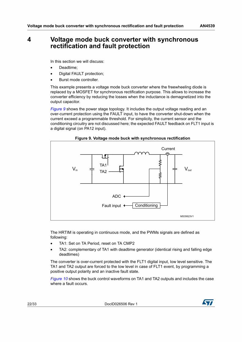
This example presents a voltage mode buck converter where the freewheeling diode is replaced by a MOSFET for synchronous rectification purpose. This allows to increase the converter efficiency by reducing the losses when the inductance is demagnetized into the output capacitor.
Figure 9 shows the power stage topology. It includes the output voltage reading and an over-current protection using the FAULT input, to have the converter shut-down when the current exceed a programmable threshold. For simplicity, the current sensor and the conditioning circuitry are not discussed here; the expected FAULT feedback on FLT1 input is a digital signal (on PA12 input).
Figure 9. Voltage mode buck with synchronous rectification
The HRTIM is operating in continuous mode, and the PWMs signals are defined as following:
• TA1: Set on TA Period, reset on TA CMP2
• TA2: complementary of TA1 with deadtime generator (identical rising and falling edge deadtimes)
The converter is over-current protected with the FLT1 digital input, low level sensitive. The TA1 and TA2 output are forced to the low level in case of FLT1 event, by programming a positive output polarity and an inactive fault state.
Figure 10 shows the buck control waveforms on TA1 and TA2 outputs and includes the case where a fault occurs.

DocID026506 Rev 1 23/33
AN4539 Voltage mode buck converter with synchronous rectification and fault protection
32
Figure 10. Buck operation with FAULT
Buck with synchronous rectification demo overview
The duty cycle on TA1 is continuously varied in an interrupt service routine generated on repetition event, to mimic a real converter management. The FAULT1 input is enabled on PA12 (active low) to demonstrate PWM shut down (low level sensitive), for both TA1 and TA2.
When the fault is triggered (PA12 input connected to GND, TA1 and TA2 signals are shut-down. The system can be re-armed by pressing the user button.
LEDs are indicating the following:
• Blue LED: blinks during normal operation;
• Red LED: blinks when FAULT is triggered;
• Orange LED: indicates the occurrence and duration of the PWM update ISR.
The ADC is configured to have conversions triggered in the middle of the converter ON time, on PA1 (Vin) and PA3 (Vout) inputs. To run the demo, the Vout input of the BUCK-BOOST converter must be connected to the 5V_O supply. The resulting voltage is available on Vout pin.
Note: To have the Discovery kit’s BOOST stage bypassed, the PA11 pin must be forced at 1 (to have the T6 PMOS switched ON).
Demo code
The example code is provided in the HRTIM_BuckSyncRect example.

Non-inverting buck-boost converter AN4539
24/33 DocID026506 Rev 1
5 Non-inverting buck-boost converter
In this section we will discuss:
• 4-switches converter drive;
• 0% and 100% PWM generation.
This example shows how to configure the HRTIM to drive a non-inverter buck-boost converter and switch on the fly from a step-down to a step-up mode. Although this configuration requires more switches than the conventional inverting buck-boost, it has the advantage of providing ground-referred positive output voltage.
Figure 11 shows the power stage topology, as implemented on the STM32F334 Discovery board.
Figure 11. Non-inverting buck-boost converter
Figure 12 summarizes the 3 operating modes of the demo with simplified schematics (MOSFETs anti-parallel diodes aren’t represented). The synchronous rectification schemes are applied for both buck and boost modes (the complementary MOSFETs are driven to reduce the conduction losses in their intrinsic diodes). A 3rd mode “de-energizing” is necessary to avoid having current flowing back into the input source when the converter is switched from boost to buck mode: the MCU maintains this mode until the output capacitor is discharged below the input voltage.
The constant ON/OFF states are imposed by forcing either 0% or 100% PWM on the complementary outputs driving the half-bridges.

DocID026506 Rev 1 25/33
AN4539 Non-inverting buck-boost converter
32
Figure 12. Buck-boost operating mode
The HRTIM is operating in continuous mode, and the PWMs signals are defined as follows:
• TA1: Set on TA CMP1, reset on TA Period;
• TA2: complementary of TA1 with deadtime generator (identical rising and falling edge deadtimes);
• TB1: Set on TB CMP1, reset on TB Period;
• TB2: complementary of TB1 with deadtime generator (identical rising and falling edge deadtimes).
The converter is protected with the FLT1 digital input, low level sensitive. All outputs are forced to the low level in case of FLT1 event, by programming a positive output polarity and an inactive fault state.
Figure 13 shows the buck-boost control waveforms on the 4 outputs for the 3 operating modes.
Figure 13. Buck-boost converter operating waveforms

Non-inverting buck-boost converter AN4539
26/33 DocID026506 Rev 1
The 0% and 100% duty cycle are obtained by programming compare register values to 0 or 100%, causing the two complementary outputs to be constantly ON/OFF:
• when CMP1 value is equal to the PER value, the duty cycle is 100% (CMP1 set event wins over PER reset event: refer to the hardware priority scheme detailled in the reference manual: when two simultaneous events are occuring, priority is the following: CMP4>CMP3>CMP2>CMP1>PER);
• when CMP1 value is above to the PER value, the duty cycle is 0% (no more set event generated).
Buck-boost demo overview
To run the demo, the Vin input pin of the BUCK-BOOST converter must be connected to the 5V_O output pin of the STM32F334 discovery kit.supply. The resulting voltage is available on Vout pin.
The demo starts in BUCK mode, and the duty cycle is slowly adjusted in the TIMA IRQ handler to have Vout continuously varying below Vin value. If the push-button is pressed and the voltage is below 5V, the boost mode is enabled (the voltage check prevents exceeding the discovery kit max output voltage). The voltage is increased above Vin value with a fixed duty cycle. If the push-button is pressed again, the output capacitor is first de-energized down to 4.5V before re-enabling the buck mode.
The ADC is configured to have conversions triggered in the middle of the converter ON time, on PA1 (Vin) and PA3 (Vout) inputs. The values are converted in mV in the main routine to have a direct voltage reading with the debugger (using a run-time refreshed watch) during the demo.
The FAULT1 input is enabled on PA12 (active low) to demonstrate PWM shut down (low level sensitive), for all outputs. When the fault is triggered (PA12 input connected to GND), TA1, TA2, TB1, TB2 signals are shut-down. The system can be re-armed by pressing the user button.
LEDs are indicating the following:
• Green LED: blinks during BUCK operation
• Blue LED: blinks during BOOST operation
• Red LED: blinks when FAULT is triggered
• Orange LED: indicates the occurrence and duration of the PWM update ISR.
Demo code
The example code is provided in the HRTIM_BuckBoost example.

DocID026506 Rev 1 27/33
AN4539 Transition mode power factor controller
32
6 Transition mode power factor controller
In this section we will discuss:
• External events conditioning and filtering;
• Timer counter reset;
• Events blanking windows;
• Capture unit;
• Constant Ton time converter.
This example presents a transition mode (also known as boundary conduction mode) power factor controller (PFC).
Figure 14 shows the topology, similar to a boost converter. It features an output voltage reading and a demagnetisation detection winding coupled with the main inductor for zero-current detection.
Figure 14. Transition mode PFC
The basic operating principle is to build-up current into an inductor during a fixed Ton time.
This current will then decay during the Toff time, and the period will be re-started when it becomes null. This is detected using a Zero Crossing Detection circuitry (ZCD), practically made of an auxiliary winding on the main inductor. With a constant Ton, the peak current value in the inductor is directly proportional to the rectified AC input voltage, which provides power factor correction.
This converter is operating with a constant Ton and a variable frequency due the Toff variation (depending on the input voltage). It must also include some features to operate when no zero-crossing is detected, or to limit Ton in case of over-current (OC). The OC feedback is usually conditioned with the built-in comparator and routed onto an external event channel.
Note: The operating principle below can also be applied for a constant off time converter.

Transition mode power factor controller AN4539
28/33 DocID026506 Rev 1
Figure 15 and Figure 16 show the waveforms during the various operating mode, with the following parameters defined:
• Ton min: during this period, spurious over-currents are discarded (typically these are freewheeling diode recovery currents). It is represented as OC blanking and programmed with CMP3;
• Ton max: practically, the converter set-point. It is defined with CMP1;
• Toff min: limits the frequency when current limit is close to zero (demagnetization is very fast). It is defined with CMP2 in auto-delayed mode;
• Toff max: prevents the system to be stuck if no ZCD occurs. It is defined with CMP4 in auto-delayed mode.
Figure 15. Transition mode PFC operation at Ton max and during over-current

DocID026506 Rev 1 29/33
AN4539 Transition mode power factor controller
32
Figure 16. Transition mode PFC operation at Toff max and Toff min
The HRTIM is operating in continuous mode, and the TD1 signal is defined as follows:
• Set on (TD CMP4 or (ZCDlatched. TDCMP2))
• Reset on (TD CMP1 or (OC. TDCMP3))
ZCDlatched. TDCMP2 indicates that ZCD event is filtered by a blanking window starting from Timer D counter reset and finishing at TD CMP2 match. The ZCD event is latched: if it occurs during the blanking window, its is not discarded and is effective at the end of the blanking period. The ZCD signal is applied on the External Event 4.
OC. TDCMP3 indicates that OC event is filtered by a blanking window starting from Timer D counter reset and finishing at TD CMP3 match. The OC event is not latched: if it occurs during the blanking window, it’s discarded. The OC signal is applied on the External Event 3.
Both Toff values (based on CMP2 and CMP4) are auto-delayed: these timings must be relative to the output signal falling edge (occurring either on CMP1 match or OC event). CMP2 and CMP4 events are generated in autodelayed mode with CMP1 timeout, based on capture1 and capture 2 events respectively. The two capture units are triggered by the OC signal (EEV3).
The timer D counter is reset either by the ZCD event or by CMP4 match (in timeout conditions).

Transition mode power factor controller AN4539
30/33 DocID026506 Rev 1
The converter is protected with the FLT1 digital input, low level sensitive. The TD1 output is forced to a low level in case of FLT1 event, by programming a positive output polarity and an inactive fault state.
Transition mode PFC demo overview
To run the demo and test all operating modes, it is necessary to simulate the feedback 2 input signals with a function generator:
• Over-current (OC, on EEV3/PB7);
• Zero-crossing detection (ZCD, on EEV4/PB6).
The various operating modes can be tested as following:
• if the OC signal is generated during the Ton time, the pulse will be shortened;
• the ZCD signal is resetting the timer counter and will cause the switching frequency to be changed accordingly.
The FAULT1 input is enabled on PA12 (active low) to demonstrate PWM shut down (low level sensitive). When the fault is triggered (PA12 input connected to GND, TD1 signal is stopped. The system can be re-armed by pressing the user button.
LEDs are indicating the following:
• Green LED: blinks during normal operation;
• Orange LED: blinks when FAULT is triggered.
Demo code
The example code is provided in the HRTIM_TM_PFC example.

DocID026506 Rev 1 31/33
AN4539 Other examples
32
7 Other examples
The cookbook will gradually be extended.
More examples to come soon, please check out the STM32F334 page on www.st.com.

Revision history AN4539
32/33 DocID026506 Rev 1
8 Revision history
Table 3. Document revision history
Date Revision Changes
19-Jun-2014 1 Initial release.

DocID026506 Rev 1 33/33
AN4539
33
Please Read Carefully:
Information in this document is provided solely in connection with ST products. STMicroelectronics NV and its subsidiaries (“ST”) reserve the right to make changes, corrections, modifications or improvements, to this document, and the products and services described herein at any time, without notice.
All ST products are sold pursuant to ST’s terms and conditions of sale.
Purchasers are solely responsible for the choice, selection and use of the ST products and services described herein, and ST assumes no liability whatsoever relating to the choice, selection or use of the ST products and services described herein.
No license, express or implied, by estoppel or otherwise, to any intellectual property rights is granted under this document. If any part of this document refers to any third party products or services it shall not be deemed a license grant by ST for the use of such third party products or services, or any intellectual property contained therein or considered as a warranty covering the use in any manner whatsoever of such third party products or services or any intellectual property contained therein.
UNLESS OTHERWISE SET FORTH IN ST’S TERMS AND CONDITIONS OF SALE ST DISCLAIMS ANY EXPRESS OR IMPLIED WARRANTY WITH RESPECT TO THE USE AND/OR SALE OF ST PRODUCTS INCLUDING WITHOUT LIMITATION IMPLIED WARRANTIES OF MERCHANTABILITY, FITNESS FOR A PARTICULAR PURPOSE (AND THEIR EQUIVALENTS UNDER THE LAWS OF ANY JURISDICTION), OR INFRINGEMENT OF ANY PATENT, COPYRIGHT OR OTHER INTELLECTUAL PROPERTY RIGHT.
ST PRODUCTS ARE NOT DESIGNED OR AUTHORIZED FOR USE IN: (A) SAFETY CRITICAL APPLICATIONS SUCH AS LIFE SUPPORTING, ACTIVE IMPLANTED DEVICES OR SYSTEMS WITH PRODUCT FUNCTIONAL SAFETY REQUIREMENTS; (B) AERONAUTIC APPLICATIONS; (C) AUTOMOTIVE APPLICATIONS OR ENVIRONMENTS, AND/OR (D) AEROSPACE APPLICATIONS OR ENVIRONMENTS. WHERE ST PRODUCTS ARE NOT DESIGNED FOR SUCH USE, THE PURCHASER SHALL USE PRODUCTS AT PURCHASER’S SOLE RISK, EVEN IF ST HAS BEEN INFORMED IN WRITING OF SUCH USAGE, UNLESS A PRODUCT IS EXPRESSLY DESIGNATED BY ST AS BEING INTENDED FOR “AUTOMOTIVE, AUTOMOTIVE SAFETY OR MEDICAL” INDUSTRY DOMAINS ACCORDING TO ST PRODUCT DESIGN SPECIFICATIONS. PRODUCTS FORMALLY ESCC, QML OR JAN QUALIFIED ARE DEEMED SUITABLE FOR USE IN AEROSPACE BY THE CORRESPONDING GOVERNMENTAL AGENCY.
Resale of ST products with provisions different from the statements and/or technical features set forth in this document shall immediately void any warranty granted by ST for the ST product or service described herein and shall not create or extend in any manner whatsoever, any liability of ST.
ST and the ST logo are trademarks or registered trademarks of ST in various countries.Information in this document supersedes and replaces all information previously supplied.
The ST logo is a registered trademark of STMicroelectronics. All other names are the property of their respective owners.
© 2014 STMicroelectronics - All rights reserved
STMicroelectronics group of companies
Australia - Belgium - Brazil - Canada - China - Czech Republic - Finland - France - Germany - Hong Kong - India - Israel - Italy - Japan - Malaysia - Malta - Morocco - Philippines - Singapore - Spain - Sweden - Switzerland - United Kingdom - United States of America
www.st.com