an3552, analog comparator tips and tricks for the mc9s08qg...
TRANSCRIPT

Freescale SemiconductorApplication Note
Document Number: AN3552Rev. 0, 11/2007
Contents
Introduction . . . . . . . . . . . . . . . . . . . . . . . . . . . . . . . . . . . 11.1 What Is an Analog Comparator? . . . . . . . . . . . . . . 1Function Description . . . . . . . . . . . . . . . . . . . . . . . . . . . . 2
2.1 Function 1: Battery Voltage Monitor . . . . . . . . . . . . 32.2 Function 2: Hysteresis Implementation . . . . . . . . . . 42.3 Function 3: Pulse-Width Measurement . . . . . . . . . . 62.4 Function 4: DC Offset Elimination . . . . . . . . . . . . . 82.5 Function 5: Voltage Doubler . . . . . . . . . . . . . . . . . 102.6 Function 6: Zero Crossing Detector . . . . . . . . . . . 122.7 Function 7: Auto Turn Off . . . . . . . . . . . . . . . . . . . 142.8 Function 8: Fixed Number Pulse Generation . . . . 16Conclusion. . . . . . . . . . . . . . . . . . . . . . . . . . . . . . . . . . . 20
ppendix A Code Listings . . . . . . . . . . . . . . . . . . . . . . . . . . . 21A.1 CODE_1: Basic Initialization Program (for
Functions 1, 2, 4–7) . . . . . . . . . . . . . . . . . . . . . . 21A.2 CODE_2: Pulse-Width Measurement (for
Function 3) . . . . . . . . . . . . . . . . . . . . . . . . . . . . . 22A.3 CODE_3: Fixed Number Pulse Generation (for
Function 8) . . . . . . . . . . . . . . . . . . . . . . . . . . . . . 23
Analog Comparator Tips and Tricks for the MC9S08QG MCU
1 IntroductionThe purpose of the document is to explain the multiple uses of the built-in analog comparator of the MC9S08QG8 microcontroller. This note explains each application, implementation information, and provides tips to gain optimal performance. All the applications are performed using the DEMO9S08QG8 board.
1.1 What Is an Analog Comparator?
An analog comparator, as its name implies, compares a signal voltage on one input of the comparator with a reference voltage on the other input and provides a 1 or 0 output when one of the signals is greater than the other.
The analog comparator module on the MC9S08QG8 operates across the full range of the supply voltage (rail-to-rail operation). Its external pins consist of a non-inverting input (ACMP+), an inverting input (ACMP–), and an optional output pin (ACMPO). The non-inverting input can also be connected to the internal
1
2
3A
© Freescale Semiconductor, Inc., 2007. All rights reserved.

Function Description
bandgap reference. The output of the comparator can be connected to the output pin, to a timer input capture channel, or left unconnected to generate an interrupt. The output of the comparator is 1 when V+ > V– and 0 when V+ < V– (see Figure 1). Further details of the analog comparator module can be found in the MC9S08QG8 data book.
Figure 1. Analog Comparator Module Block Diagram
2 Function DescriptionThe following examples show the utility of the analog comparator module (ACMP) on many of the Freescale HCS08 microcontrollers (MCUs). All the applications in this document are performed using the DEMO9S08QG8 board and can be replicated with other HCS08 MCUs and microcontroller demo boards. The software for each example was developed using the CodeWarrior toolset.
NOTEVerify that jumpers 5 and 6 on the USER_EN connector are not present on the DEMO9S08QG8 board. If the USB voltage is used to power the demo board, the PWR_SEL jumper must be in the VB position. If an external power source is selected for the demo board, the PWR_SEL jumper should be in the VDD position.
Analog Comparator Tips and Tricks for the MC9S08QG MCU, Rev. 0
Freescale Semiconductor2
Function Description
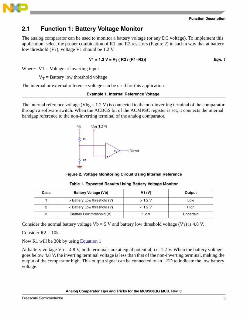
2.1 Function 1: Battery Voltage MonitorThe analog comparator can be used to monitor a battery voltage (or any DC voltage). To implement this application, select the proper combination of R1 and R2 resistors (Figure 2) in such a way that at battery low threshold (VT), voltage V1 should be 1.2 V.
V1 = 1.2 V = VT ( R2 / (R1+R2)) Eqn. 1
Where: V1 = Voltage at inverting input
VT = Battery low threshold voltage
The internal or external reference voltage can be used for this application.
Example 1. Internal Reference Voltage
The internal reference voltage (Vbg = 1.2 V) is connected to the non-inverting terminal of the comparator through a software switch. When the ACBGS bit of the ACMPSC register is set, it connects the internal bandgap reference to the non-inverting terminal of the analog comparator.
Figure 2. Voltage Monitoring Circuit Using Internal Reference
Consider the normal battery voltage Vb = 5 V and battery low threshold voltage (VT) is 4.8 V.
Consider R2 = 10k
Now R1 will be 30k by using Equation 1
At battery voltage Vb = 4.8 V, both terminals are at equal potential, i.e. 1.2 V. When the battery voltage goes below 4.8 V, the inverting terminal voltage is less than that of the non-inverting terminal, making the output of the comparator high. This output signal can be connected to an LED to indicate the low battery voltage.
Table 1. Expected Results Using Battery Voltage Monitor
Case Battery Voltage (Vb) V1 (V) Output
1 > Battery Low threshold (V) > 1.2 V Low
2 < Battery Low threshold (V) < 1.2 V High
3 Battery Low threshold (V) 1.2 V Uncertain
Analog Comparator Tips and Tricks for the MC9S08QG MCU, Rev. 0
Freescale Semiconductor 3
Function Description
The necessary code for this example is shown in Section A.1, “CODE_1: Basic Initialization Program (for Functions 1, 2, 4–7).” For this example, the MCU_init function must have ACMPSC_ACBGS = 1 and SPMSC1_BGBE = 1 to enable the internal reference.
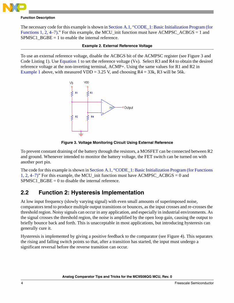
Example 2. External Reference Voltage
To use an external reference voltage, disable the ACBGS bit of the ACMPSC register (see Figure 3 and Code Listing 1). Use Equation 1 to set the reference voltage (VR). Select R3 and R4 to obtain the desired reference voltage at the non-inverting terminal, ACMP+. Using the same values for R1 and R2 in Example 1 above, with measured VDD = 3.25 V, and choosing R4 = 33k, R3 will be 56k.
Figure 3. Voltage Monitoring Circuit Using External Reference
To prevent constant draining of the battery through the resistors, a MOSFET can be connected between R2 and ground. Whenever intended to monitor the battery voltage, the FET switch can be turned on with another port pin.
The code for this example is shown in Section A.1, “CODE_1: Basic Initialization Program (for Functions 1, 2, 4–7)” For this example, the MCU_init function must have ACMPSC_ACBGS = 0 and SPMSC1_BGBE = 0 to disable the internal reference.
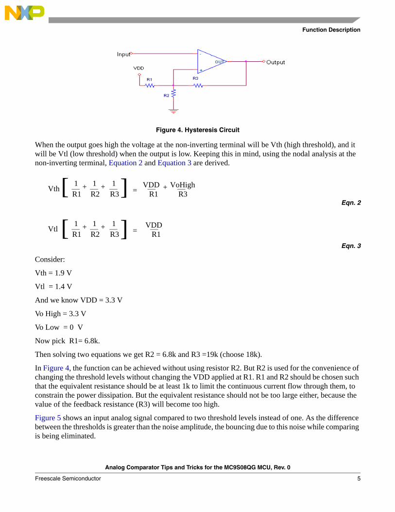
2.2 Function 2: Hysteresis ImplementationAt low input frequency (slowly varying signal) with even small amounts of superimposed noise, comparators tend to produce multiple output transitions or bounces, as the input crosses and re-crosses the threshold region. Noisy signals can occur in any application, and especially in industrial environments. As the signal crosses the threshold region, the noise is amplified by the open loop gain, causing the output to briefly bounce back and forth. This is unacceptable in most applications, but introducing hysteresis can generally cure it.
Hysteresis is implemented by giving a positive feedback to the comparator (see Figure 4). This separates the rising and falling switch points so that, after a transition has started, the input must undergo a significant reversal before the reverse transition can occur.
Analog Comparator Tips and Tricks for the MC9S08QG MCU, Rev. 0
Freescale Semiconductor4
Function Description
Figure 4. Hysteresis Circuit
When the output goes high the voltage at the non-inverting terminal will be Vth (high threshold), and it will be Vtl (low threshold) when the output is low. Keeping this in mind, using the nodal analysis at the non-inverting terminal, Equation 2 and Equation 3 are derived.
Eqn. 2
Eqn. 3
Consider:
Vth = 1.9 V
Vtl = 1.4 V
And we know VDD = 3.3 V
Vo High = 3.3 V
Vo Low = 0 V
Now pick R1= 6.8k.
Then solving two equations we get R2 = 6.8k and R3 =19k (choose 18k).
In Figure 4, the function can be achieved without using resistor R2. But R2 is used for the convenience of changing the threshold levels without changing the VDD applied at R1. R1 and R2 should be chosen such that the equivalent resistance should be at least 1k to limit the continuous current flow through them, to constrain the power dissipation. But the equivalent resistance should not be too large either, because the value of the feedback resistance (R3) will become too high.
Figure 5 shows an input analog signal compared to two threshold levels instead of one. As the difference between the thresholds is greater than the noise amplitude, the bouncing due to this noise while comparing is being eliminated.
Vth[ 1R1
1R2
1R3
+ + =] VDD
R1VoHigh
R3+
Vtl1R1
1R2
1R3
+ + =VDD
R1[ ]
Analog Comparator Tips and Tricks for the MC9S08QG MCU, Rev. 0
Freescale Semiconductor 5
Function Description
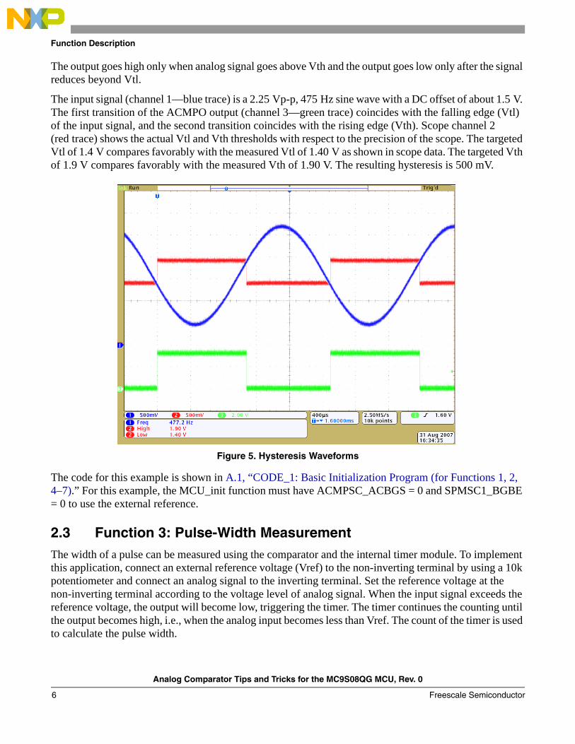
The output goes high only when analog signal goes above Vth and the output goes low only after the signal reduces beyond Vtl.
The input signal (channel 1—blue trace) is a 2.25 Vp-p, 475 Hz sine wave with a DC offset of about 1.5 V. The first transition of the ACMPO output (channel 3—green trace) coincides with the falling edge (Vtl) of the input signal, and the second transition coincides with the rising edge (Vth). Scope channel 2 (red trace) shows the actual Vtl and Vth thresholds with respect to the precision of the scope. The targeted Vtl of 1.4 V compares favorably with the measured Vtl of 1.40 V as shown in scope data. The targeted Vth of 1.9 V compares favorably with the measured Vth of 1.90 V. The resulting hysteresis is 500 mV.
Figure 5. Hysteresis Waveforms
The code for this example is shown in A.1, “CODE_1: Basic Initialization Program (for Functions 1, 2, 4–7).” For this example, the MCU_init function must have ACMPSC_ACBGS = 0 and SPMSC1_BGBE = 0 to use the external reference.
2.3 Function 3: Pulse-Width MeasurementThe width of a pulse can be measured using the comparator and the internal timer module. To implement this application, connect an external reference voltage (Vref) to the non-inverting terminal by using a 10k potentiometer and connect an analog signal to the inverting terminal. Set the reference voltage at the non-inverting terminal according to the voltage level of analog signal. When the input signal exceeds the reference voltage, the output will become low, triggering the timer. The timer continues the counting until the output becomes high, i.e., when the analog input becomes less than Vref. The count of the timer is used to calculate the pulse width.
Analog Comparator Tips and Tricks for the MC9S08QG MCU, Rev. 0
Freescale Semiconductor6
Function Description
Figure 6. Pulse Width Measurement Circuit
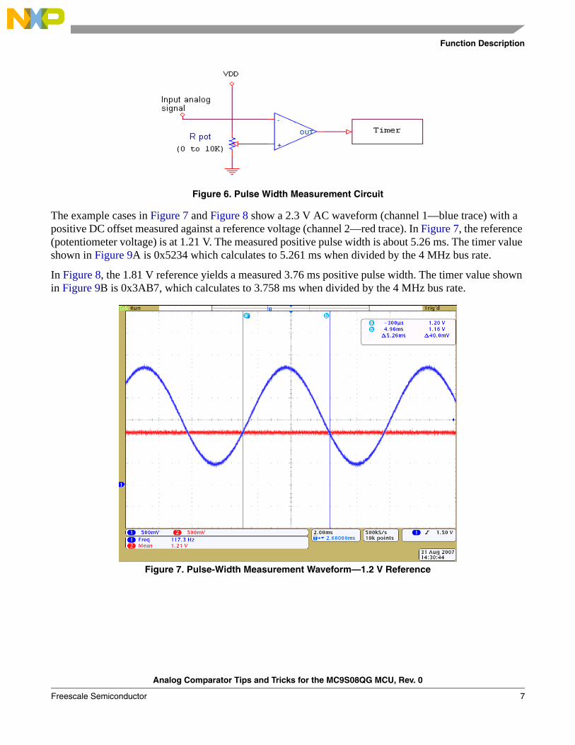
The example cases in Figure 7 and Figure 8 show a 2.3 V AC waveform (channel 1—blue trace) with a positive DC offset measured against a reference voltage (channel 2—red trace). In Figure 7, the reference (potentiometer voltage) is at 1.21 V. The measured positive pulse width is about 5.26 ms. The timer value shown in Figure 9A is 0x5234 which calculates to 5.261 ms when divided by the 4 MHz bus rate.
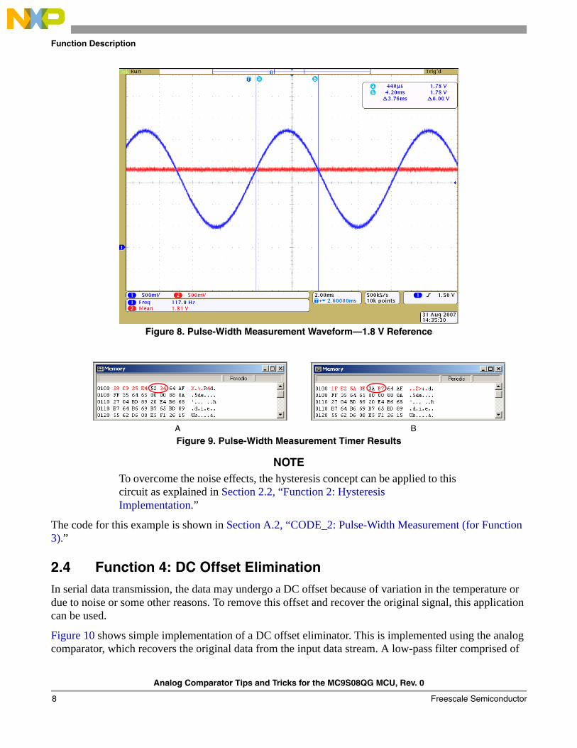
In Figure 8, the 1.81 V reference yields a measured 3.76 ms positive pulse width. The timer value shown in Figure 9B is 0x3AB7, which calculates to 3.758 ms when divided by the 4 MHz bus rate.
Figure 7. Pulse-Width Measurement Waveform—1.2 V Reference
Analog Comparator Tips and Tricks for the MC9S08QG MCU, Rev. 0
Freescale Semiconductor 7
Function Description
Figure 8. Pulse-Width Measurement Waveform—1.8 V Reference
Figure 9. Pulse-Width Measurement Timer Results
NOTETo overcome the noise effects, the hysteresis concept can be applied to this circuit as explained in Section 2.2, “Function 2: Hysteresis Implementation.”
The code for this example is shown in Section A.2, “CODE_2: Pulse-Width Measurement (for Function 3).”
2.4 Function 4: DC Offset Elimination
In serial data transmission, the data may undergo a DC offset because of variation in the temperature or due to noise or some other reasons. To remove this offset and recover the original signal, this application can be used.
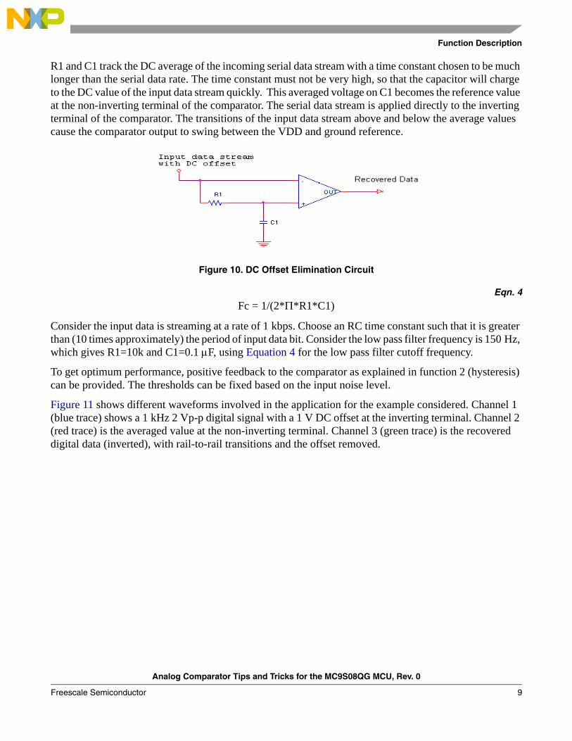
Figure 10 shows simple implementation of a DC offset eliminator. This is implemented using the analog comparator, which recovers the original data from the input data stream. A low-pass filter comprised of
A B
Analog Comparator Tips and Tricks for the MC9S08QG MCU, Rev. 0
Freescale Semiconductor8
Function Description
R1 and C1 track the DC average of the incoming serial data stream with a time constant chosen to be much longer than the serial data rate. The time constant must not be very high, so that the capacitor will charge to the DC value of the input data stream quickly. This averaged voltage on C1 becomes the reference value at the non-inverting terminal of the comparator. The serial data stream is applied directly to the inverting terminal of the comparator. The transitions of the input data stream above and below the average values cause the comparator output to swing between the VDD and ground reference.
Figure 10. DC Offset Elimination Circuit
Eqn. 4
Consider the input data is streaming at a rate of 1 kbps. Choose an RC time constant such that it is greater than (10 times approximately) the period of input data bit. Consider the low pass filter frequency is 150 Hz, which gives R1=10k and C1=0.1 μF, using Equation 4 for the low pass filter cutoff frequency.
To get optimum performance, positive feedback to the comparator as explained in function 2 (hysteresis) can be provided. The thresholds can be fixed based on the input noise level.
Figure 11 shows different waveforms involved in the application for the example considered. Channel 1 (blue trace) shows a 1 kHz 2 Vp-p digital signal with a 1 V DC offset at the inverting terminal. Channel 2 (red trace) is the averaged value at the non-inverting terminal. Channel 3 (green trace) is the recovered digital data (inverted), with rail-to-rail transitions and the offset removed.
Fc = 1/(2*Π*R1*C1)
Analog Comparator Tips and Tricks for the MC9S08QG MCU, Rev. 0
Freescale Semiconductor 9

Function Description
Figure 11. DC Offset Elimination Waveforms
The code for this example is shown in A.1, “CODE_1: Basic Initialization Program (for Functions 1, 2, 4–7).” For this example, the MCU_init function must have ACMPSC_ACBGS = 0 and SPMSC1_BGBE = 0 to use the external reference.
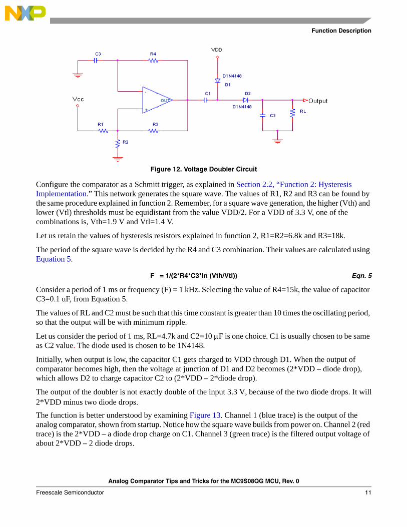
2.5 Function 5: Voltage DoublerA voltage multiplier is an electrical circuit that converts AC electrical power from a lower voltage to a higher DC voltage by means of capacitors and diodes combined into a network. The Voltage Doubler is the basic stage of the voltage multiplier. This is implemented by using the on-chip analog comparator as a square wave generator, from which the doubler action is achieved by using diode and capacitor combinations, as shown in Figure 12.
Analog Comparator Tips and Tricks for the MC9S08QG MCU, Rev. 0
Freescale Semiconductor10
Function Description
Figure 12. Voltage Doubler Circuit
Configure the comparator as a Schmitt trigger, as explained in Section 2.2, “Function 2: Hysteresis Implementation.” This network generates the square wave. The values of R1, R2 and R3 can be found by the same procedure explained in function 2. Remember, for a square wave generation, the higher (Vth) and lower (Vtl) thresholds must be equidistant from the value VDD/2. For a VDD of 3.3 V, one of the combinations is, Vth=1.9 V and Vtl=1.4 V.
Let us retain the values of hysteresis resistors explained in function 2, R1=R2=6.8k and R3=18k.
The period of the square wave is decided by the R4 and C3 combination. Their values are calculated using Equation 5.
F = 1/(2*R4*C3*ln (Vth/Vtl)) Eqn. 5
Consider a period of 1 ms or frequency (F) = 1 kHz. Selecting the value of R4=15k, the value of capacitor C3=0.1 uF, from Equation 5.
The values of RL and C2 must be such that this time constant is greater than 10 times the oscillating period, so that the output will be with minimum ripple.
Let us consider the period of 1 ms, RL=4.7k and C2=10 μF is one choice. C1 is usually chosen to be same as C2 value. The diode used is chosen to be 1N4148.
Initially, when output is low, the capacitor C1 gets charged to VDD through D1. When the output of comparator becomes high, then the voltage at junction of D1 and D2 becomes (2*VDD – diode drop), which allows D2 to charge capacitor C2 to (2*VDD – 2*diode drop).
The output of the doubler is not exactly double of the input 3.3 V, because of the two diode drops. It will2*VDD minus two diode drops.The function is better understood by examining Figure 13. Channel 1 (blue trace) is the output of the analog comparator, shown from startup. Notice how the square wave builds from power on. Channel 2 (red trace) is the 2*VDD – a diode drop charge on C1. Channel 3 (green trace) is the filtered output voltage of about 2*VDD – 2 diode drops.
Analog Comparator Tips and Tricks for the MC9S08QG MCU, Rev. 0
Freescale Semiconductor 11

Function Description
Figure 13. Voltage Doubler Waveforms
The code for this example is shown in Section A.1, “CODE_1: Basic Initialization Program (for Functions 1, 2, 4–7).” For this example, the MCU_init function must have ACMPSC_ACBGS = 0 and SPMSC1_BGBE = 0 to use the external reference.
2.6 Function 6: Zero Crossing Detector
There may be a necessity of determining the point of an AC input crossing the zero value in some situations. This can be implemented using the comparator in the MC9S08QG8 and some external components (resistors).
Figure 14. Zero Crossing Detector Circuit
Analog Comparator Tips and Tricks for the MC9S08QG MCU, Rev. 0
Freescale Semiconductor12

Function Description
As the comparator is of single reference, we cannot directly apply the bipolar signal as input to it. So an offset needs to be added to the signal through R1 and R2 (see Figure 14). When the input signal is zero, the voltages at both inverting and non-inverting terminals are the same. Whenever the input crosses zero, the voltage at the inverting terminal becomes higher or lower than (depending on the polarity of the input) the reference at non-inverting terminals, making the output LOW or HIGH respectively.
We can pick R1=R2=10k as one good choice as it gives an offset of VDD/2, enabling the input to have maximum swing above and below the offset. The analog signals at the inverting terminal must not exceed the maximum ratings of the comparator inputs (–0.3 to 3.8 V).
The addition of positive feedback, as explained in Section 2.2, “Function 2: Hysteresis Implementation,” gives better results, if the input has any noise along with it.
In Figure 15, channel 1 (blue trace) is a 200 Hz sine wave with a 5.68 V peak-to-peak amplitude and 0 V DC offset. It has negative transitions that exceed the comparator’s input ratings. Channel 2 (red trace) is the offset signal into the comparator’s inverting input. Its amplitude is contained within the comparator’s valid input values of VDD and ground. Channel 3 (green trace) is the output of the comparator, which transitions at each zero crossing of the input AC signal. The comparator output would typically be fed to a timer channel or to an interrupt.
Figure 15. Zero Crossing Detector Waveforms
The code for this example is shown in Section A.1, “CODE_1: Basic Initialization Program (for Functions 1, 2, 4–7).” For this example, the MCU_init function must have ACMPSC_ACBGS = 0 and SPMSC1_BGBE = 0 to use the external reference.
Analog Comparator Tips and Tricks for the MC9S08QG MCU, Rev. 0
Freescale Semiconductor 13
Function Description
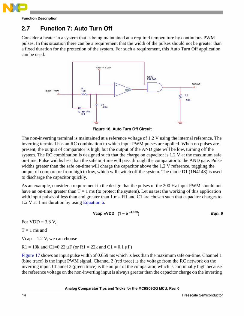
2.7 Function 7: Auto Turn Off Consider a heater in a system that is being maintained at a required temperature by continuous PWM pulses. In this situation there can be a requirement that the width of the pulses should not be greater than a fixed duration for the protection of the system. For such a requirement, this Auto Turn Off application can be used.
Figure 16. Auto Turn Off Circuit
The non-inverting terminal is maintained at a reference voltage of 1.2 V using the internal reference. The inverting terminal has an RC combination to which input PWM pulses are applied. When no pulses are present, the output of comparator is high, but the output of the AND gate will be low, turning off the system. The RC combination is designed such that the charge on capacitor is 1.2 V at the maximum safe on-time. Pulse widths less than the safe on-time will pass through the comparator to the AND gate. Pulse widths greater than the safe on-time will charge the capacitor above the 1.2 V reference, toggling the output of comparator from high to low, which will switch off the system. The diode D1 (1N4148) is used to discharge the capacitor quickly.
As an example, consider a requirement in the design that the pulses of the 200 Hz input PWM should not have an on-time greater than T = 1 ms (to protect the system). Let us test the working of this application with input pulses of less than and greater than 1 ms. R1 and C1 are chosen such that capacitor charges to 1.2 V at 1 ms duration by using Equation 6.
Vcap =VDD (1 – e –T/RC) Eqn. 6
For VDD = 3.3 V,
T = 1 ms and
Vcap = 1.2 V, we can choose
R1 = 10k and C1=0.22 μF (or R1 = 22k and C1 = 0.1 μF)
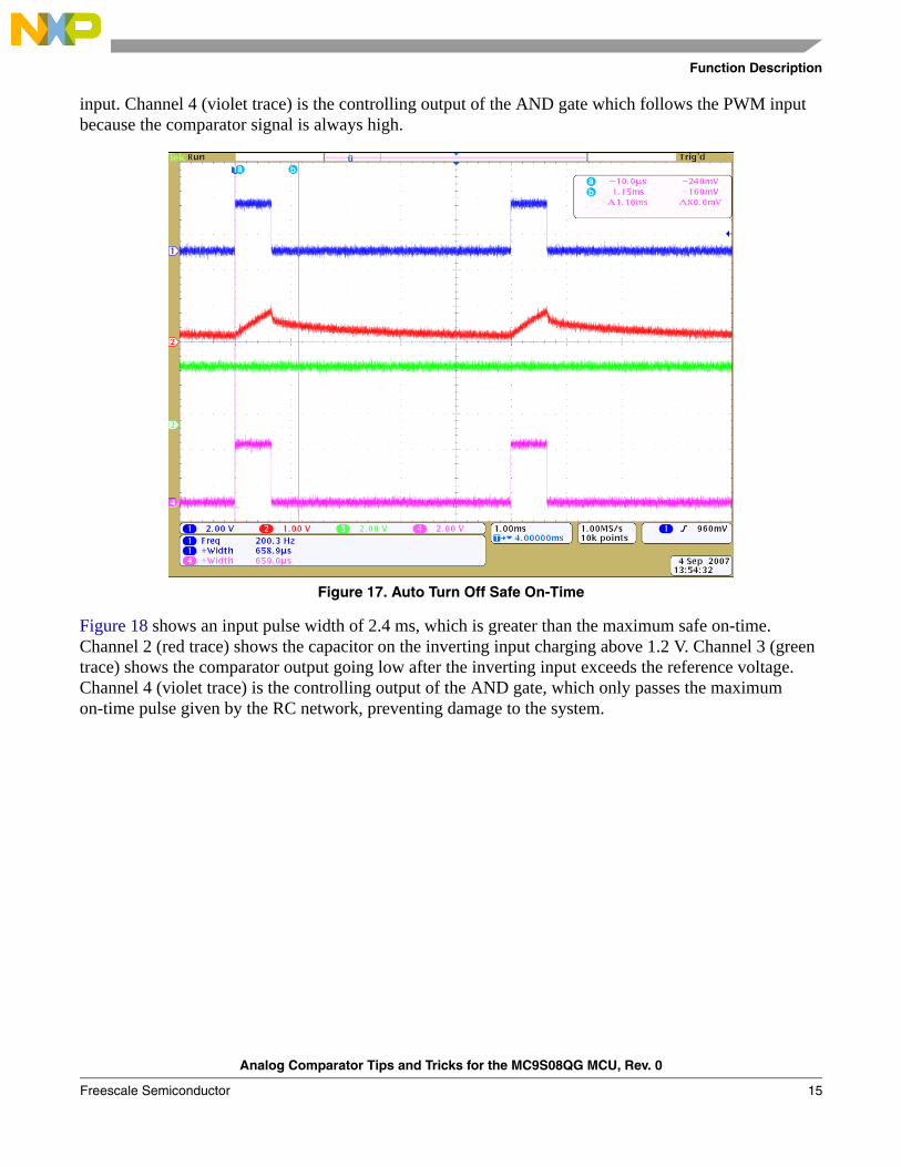
Figure 17 shows an input pulse width of 0.659 ms which is less than the maximum safe on-time. Channel 1 (blue trace) is the input PWM signal. Channel 2 (red trace) is the voltage from the RC network on the inverting input. Channel 3 (green trace) is the output of the comparator, which is continually high because the reference voltage on the non-inverting input is always greater than the capacitor charge on the inverting
Analog Comparator Tips and Tricks for the MC9S08QG MCU, Rev. 0
Freescale Semiconductor14
Function Description
input. Channel 4 (violet trace) is the controlling output of the AND gate which follows the PWM input because the comparator signal is always high.
Figure 17. Auto Turn Off Safe On-Time
Figure 18 shows an input pulse width of 2.4 ms, which is greater than the maximum safe on-time. Channel 2 (red trace) shows the capacitor on the inverting input charging above 1.2 V. Channel 3 (green trace) shows the comparator output going low after the inverting input exceeds the reference voltage. Channel 4 (violet trace) is the controlling output of the AND gate, which only passes the maximum on-time pulse given by the RC network, preventing damage to the system.
Analog Comparator Tips and Tricks for the MC9S08QG MCU, Rev. 0
Freescale Semiconductor 15

Function Description
Figure 18. Auto Turn Off Exceeding Safe On-Time
The code for this example is shown in A.1, “CODE_1: Basic Initialization Program (for Functions 1, 2, 4–7).” For this example, the MCU_init function must have ACMPSC_ACBGS = 1 and SPMSC1_BGBE = 1 to use the internal reference.
2.8 Function 8: Fixed Number Pulse GenerationThe ACMP module can be used to generate a fixed number of pulses at its output. The comparator is configured as a square wave generator format as shown in Figure 19. The design of this square wave generator is same as that mentioned in Section 2.5, “Function 5: Voltage Doubler.”
Analog Comparator Tips and Tricks for the MC9S08QG MCU, Rev. 0
Freescale Semiconductor16

Function Description
Figure 19. Fixed Number Pulse Generator Circuit
Then, by using software we can control the number of positive pulses coming out of the comparator/square wave generator. The code is shown in Section A.3, “CODE_3: Fixed Number Pulse Generation (for Function 8).”
Initially, the comparator is not enabled in its initialization in the MCU_init function. The clock used is the internal bus clock, which is derived by dividing the internal clock source by 8 to get a 1 MHz bus frequency. The keyboard interrupt (KBI) module is enabled and used to detect when a switch is pressed. The KBI interrupt is used to start the modulo timer (MTIM) module and the ACMP module. The counter frequency of the MTIM is set to operate at (1 MHz/256) = 3906 Hz, by writing 8 into the MTIMCLK prescaler register. Now, the number of pulses coming at the output of comparator is controlled by enabling the ACMP module (ACMP_ACME=1) for a fixed duration. This is done by writing a value into the MTIMMOD register, up to which the module counter gets incremented and overflows. The MTIM interrupt generated at this overflow is used to disable the comparator. The comparator module is enabled for a period (MTIMMOD/ counter frequency).
For example, consider that the square wave setup of the ACMP can generate pulses at a frequency of 1 kHz, i.e., each pulse is a period of 1 ms. Assume that the requirement is to generate 5 to 20 positive pulses from the comparator.
Before continuing, we must consider experimental results that show that we need to precharge the C3 capacitor to avoid an unintentionally long initial pulse. Given that requirement and the tolerances of the RC components, we see that some adjustments must be considered. Figure 20 shows a discharge time of approximately 1.5 ms for the components chosen. The actual pulse period in this example is 1.07 ms, again based on the chosen RC component tolerances. Also, to get positive pulses only, turn off the comparator during the last half of the last period. The resulting relationship is:
(MTIMMOD/ frequency) = 1.5 ms + (#pulses – 0.5)*pulse period Eqn. 7
Using this relationship and the actual pulse width, we calculate the MTIMMOD values needed for 5, 10, 15, and 20 pulses (see Table 2).
Analog Comparator Tips and Tricks for the MC9S08QG MCU, Rev. 0
Freescale Semiconductor 17

Function Description
When SW1 is pressed the KBI interrupt enables the ACMP and the MTIM operating at 3906 Hz. The MTIMMOD value is written in the KBI interrupt service routine. When the MTIM overflows, it generates an interrupt that disables the ACMP, which stops the pulses and lets the ACMP output return high.
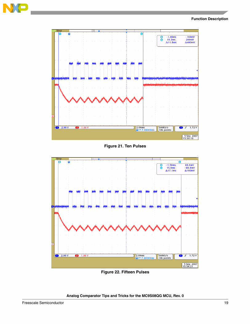
Figure 20, Figure 21, and Figure 22 show the resulting pulse trains generated using the values in the table above for 5, 10, and 15 pulses, respectively. Table 2 also shows the actual MTIM duration versus the calculated duration.
Figure 20. Five Pulses
Table 2. Fixed Pulse Number Results
# PulsesCalculated MTIM
Duration (ms)MTIMMOD (Decimal) MTIMMOD (Hex)
Actual MTIM Duration (ms)
5 6.3 24.7 18 6.45
10 11.7 45.6 2D 11.8
15 17.0 66.5 42 17.1
20 22.4 87.4 57 22.7
Analog Comparator Tips and Tricks for the MC9S08QG MCU, Rev. 0
Freescale Semiconductor18
Function Description
Figure 21. Ten Pulses
Figure 22. Fifteen Pulses
Analog Comparator Tips and Tricks for the MC9S08QG MCU, Rev. 0
Freescale Semiconductor 19

Conclusion
3 ConclusionThis application note describes several potential uses for the on-board analog comparator module on the MC9S08 microcontrollers. The demonstrated functions used the DEMO9S08QG8 board with the appropriate software. The concepts can be expanded to meet other uses as well. The CodeWarrior software project for these examples is available on the Freescale Semiconductor website.
Analog Comparator Tips and Tricks for the MC9S08QG MCU, Rev. 0
Freescale Semiconductor20

Conclusion
Appendix A Code Listings
A.1 CODE_1: Basic Initialization Program (for Functions 1, 2, 4–7)
/*----------------------------------------------------------------*//*This program basically enables the comparator, initializes the *//*comparator for output on the ACMPO pin, usage of internal *//*reference voltage at ACMP+. etc, depending on the content of *//*corresponding bits in the control registers. *//* *//*----------------------------------------------------------------*/
#include <hidef.h> /* for EnableInterrupts macro */#include "derivative.h" /* include peripheral declarations */
void MCU_init(void); /* Device initialization function declaration */
void main(void) { MCU_init();
EnableInterrupts; /* enable interrupts */ /* include your code here */
for(;;) { __RESET_WATCHDOG(); /* feeds the dog */ } /* loop forever */ /* please make sure that you never leave main */}
void MCU_init(void) { ACMPSC_ACME = 1;//enable the comparator module ACMPSC_ACOPE = 1;//analog comparator output driven out ACMPO pin ACMPSC_ACBGS = 0;//internal ref disabled for '0', enabled for '1' SOPT1_BKGDPE = 0;//PTA4/ACMPO/BKGD/MS pin functions as PTA4orACMPO ICSC2_BDIV = 1;//Divide internal clock by 2 SPMSC1_BGBE = 0;//internal ref disabled for '0', enabled for '1'}
NOTESet the bits ACMPSC_ACBGS and SPMSC1_BGBE to use the internal reference voltage, 1.2 V, at the non-inverting terminal. When using an external reference, clear the above-mentioned bits.
Analog Comparator Tips and Tricks for the MC9S08QG MCU, Rev. 0
Freescale Semiconductor 21

Conclusion
A.2 CODE_2: Pulse-Width Measurement (for Function 3)/*----------------------------------------------------------------*//*An analog signal is fed to the ACMP- pin for comparison to the *//*level on the ACMP+ pin. A falling edge on the comparator output *//*is generated when the analog signal goes above the level on *//*ACMP+. The comparator output is internally connected to the *//*timer channel 0 input capture so that the ACMP interrupt gets *//*the current timer value, and the rising-edge input capture *//*interrupt captures the time of the analog signal going below *//*the ACMP+ level. The high time (pulse width) of the analog *//*signal is the difference between the rising edge input capture *//*and the initial timer count and is saved in the pulsewidth *//*variable. *//*----------------------------------------------------------------*/
#include <hidef.h> /* for EnableInterrupts macro */#include "derivative.h" /* include peripheral declarations */ #define BYTE unsigned char#define WORD unsigned int
volatile WORD time0; volatile WORD time1; volatile WORD pulsewidth;
void MCU_init(void); /* Device initialization function declaration */
void main(void) {
MCU_init();
EnableInterrupts; /* enable interrupts */ /* include your code here */
for(;;) { __RESET_WATCHDOG(); /* feeds the dog */ } /* loop forever */ /* please make sure that you never leave main */}
void MCU_init(void) { ICSSC = NV_FTRIM;//fine trim for int osc ICSTRM = NV_ICSTRM;//trim for int osc /*comparator initialization*/ ACMPSC = 0xB2;//analog comparator enable, ext reference SPMSC1_BGBE = 0;//internal ref disabled (0), enabled (1) SOPT1_BKGDPE = 1;//PTA4/ACMPO/BKGD/MS pin functions as BKGD/MS SOPT2_ACIC = 1;//ACMP output connected to TPM input channel 0; /*clock initialization*/ ICSC2_BDIV = 1;//divide internal clock by 2 (4MHz bus) /*Timer module initialization*/ TPMSC = 0x08;//selects bus clock, divide by 1 TPMC0SC = 0x44;/*channel 0 interrupt request enabled input capture on rising edge only*/
Analog Comparator Tips and Tricks for the MC9S08QG MCU, Rev. 0
Freescale Semiconductor22

Conclusion
TPMCNTH = 0x00;//reset the counter TPMCNTL = 0x00; TPMMODH = 0x00;//make free running counter TPMMODL = 0x00;}
/*ACMP interrupt routine for comparator output falling edge*/interrupt 20 void ACMP_ISR(void) { ACMPSC_ACF = 1;//clear pending comparator interrupts time0 = TPMCNT;//signal rising edge - get timer value}
/*Timer channel 0 interrupt routine for comparator rising edge detection*/interrupt 5 void TPMCH0_ISR(void) { TPMC0SC_CH0F = 0;//clear the flag time1 = TPMC0V;//signal falling edge - capture end value pulsewidth = time1 - time0;//continuously update }
A.3 CODE_3: Fixed Number Pulse Generation (for Function 8)/*----------------------------------------------------------------*//*The comparator should be in square wave generation format *//*initially. The code enables the comparator for a fixed period *//*by using the MTIM module of the MCU to get the required number *//*of pulses at the output of ACMP. After that it is disabled in *//*the MTIM interrupt service routine. This code generates 10 *//*pulses, each of period of about 1ms. The pulses are generated *//*after a keyboard interrupt on SW1 of the QG8 demo board. *//*----------------------------------------------------------------*/
#include <hidef.h> /* for EnableInterrupts macro */#include "derivative.h" /* include peripheral declarations */#include "demo9S08QG8.h"
void MCU_init(void); /* Device initialization function declaration */
void main(void) { MCU_init(); //Intialisations are written in this function EnableInterrupts;/* enable interrupts */
/* include your code here */ for(;;) { __RESET_WATCHDOG(); /* feeds the dog */ } /* loop forever */ /* please make sure that you never leave this function */}
void MCU_init(void){
Analog Comparator Tips and Tricks for the MC9S08QG MCU, Rev. 0
Freescale Semiconductor 23

Conclusion
/* Clock Initialization. Use default 16MHz ICSOUT clock - FEI*/ ICSTRM = NV_ICSTRM;//trim the internal clock source ICSSC = NV_FTRIM;//fine trim ICSC2_BDIV = 3;//divide the internal clock by 8 for 1MHz bus /* Initialisation of Port A Pin to charge the C3 Capacitor */ PTAD_PTAD1 = 1;//drive PTA1 high to charge cap PTADD_PTADD1 = 1;//will get overriden by ACMP later /*comparator intialisation*/ ACMPSC_ACOPE = 1;//Analog comparator output is driven out on ACMPO
SOPT1_BKGDPE = 0;//PTA4/ACMPO/BKGD/MS pin functions as PTA4orACMPO. /* set port pin for LED indication, to check switch operation */ /* Note: Use If required*/ PTBDD_PTBDD6 = 1;//Set PTB7 as an output LED1 =0; //Port B6 is connected to LED 1 on QG8 demo board /*KBI Set Up for SW1*/ KBISC_KBIE = 0;//mask Keyboard Interrupts PTAPE_PTAPE2 = 1;//Enable Pullup for Keyboard pin KBIPE_KBIPE2 = 1;//Enable Keyboard Pin KBISC_KBACK = 1;//Clear Pending Keyboard Interrupts KBISC_KBIE = 1;//Enable Keyboard Interrupts /*MTIM module Initialization*/ MTIMSC_TRST = 1; MTIMSC_TSTP = 0; MTIMCLK_PS = 8;//divide the bus clock by 256 MTIMCLK_CLKS= 0;//select bus clock as source (1MHz/256)}
/* Key board interrupt service routine*/interrupt 18 void KBI_ISR(void) { KBISC_KBACK = 1;//Clear Pending Keyboard Interrupts LED1 = ~LED1; //toggle LED whenever SW1 is pressed //remove if not required MTIMMOD = 0x42;//desired count into modulo register to get discrete //pulses at ACMPO. //NOTE: The pulse period is dependent on the RC values. //MTIMMOD approx=3906*[1.5ms+(pulses-0.5)*pulse period] MTIMSC_TOIE = 1;//start MTIM, enable ints ACMPSC_ACME = 1;//Enable the ACMP}
/* MTIM_ISR - ISR to disable the comparator module */interrupt 12 void MTIM_ISR(void) { ACMPSC_ACME = 0;//Disable the ACMP}
Analog Comparator Tips and Tricks for the MC9S08QG MCU, Rev. 0
Freescale Semiconductor24

THIS PAGE IS INTENTIONALLY BLANK
Analog Comparator Tips and Tricks for the MC9S08QG MCU, Rev. 0
Freescale Semiconductor 25

Document Number: AN3552Rev. 011/2007
How to Reach Us:
Home Page:www.freescale.com
Web Support:http://www.freescale.com/support
USA/Europe or Locations Not Listed:Freescale Semiconductor, Inc.Technical Information Center, EL5162100 East Elliot RoadTempe, Arizona 85284+1-800-521-6274 or +1-480-768-2130www.freescale.com/support
Europe, Middle East, and Africa:Freescale Halbleiter Deutschland GmbHTechnical Information CenterSchatzbogen 781829 Muenchen, Germany+44 1296 380 456 (English)+46 8 52200080 (English)+49 89 92103 559 (German)+33 1 69 35 48 48 (French)www.freescale.com/support
Japan:Freescale Semiconductor Japan Ltd.HeadquartersARCO Tower 15F1-8-1, Shimo-Meguro, Meguro-ku,Tokyo 153-0064Japan0120 191014 or +81 3 5437 [email protected]
Asia/Pacific:Freescale Semiconductor Hong Kong Ltd.Technical Information Center2 Dai King StreetTai Po Industrial EstateTai Po, N.T., Hong Kong+800 2666 [email protected]
For Literature Requests Only:Freescale Semiconductor Literature Distribution CenterP.O. Box 5405Denver, Colorado 802171-800-441-2447 or 303-675-2140Fax: [email protected]
Information in this document is provided solely to enable system and software implementers to use Freescale Semiconductor products. There are no express or implied copyright licenses granted hereunder to design or fabricate any integrated circuits or integrated circuits based on the information in this document.
Freescale Semiconductor reserves the right to make changes without further notice to any products herein. Freescale Semiconductor makes no warranty, representation or guarantee regarding the suitability of its products for any particular purpose, nor does Freescale Semiconductor assume any liability arising out of the application or use of any product or circuit, and specifically disclaims any and all liability, including without limitation consequential or incidental damages. “Typical” parameters that may be provided in Freescale Semiconductor data sheets and/or specifications can and do vary in different applications and actual performance may vary over time. All operating parameters, including “Typicals”, must be validated for each customer application by customer’s technical experts. Freescale Semiconductor does not convey any license under its patent rights nor the rights of others. Freescale Semiconductor products are not designed, intended, or authorized for use as components in systems intended for surgical implant into the body, or other applications intended to support or sustain life, or for any other application in which the failure of the Freescale Semiconductor product could create a situation where personal injury or death may occur. Should Buyer purchase or use Freescale Semiconductor products for any such unintended or unauthorized application, Buyer shall indemnify and hold Freescale Semiconductor and its officers, employees, subsidiaries, affiliates, and distributors harmless against all claims, costs, damages, and expenses, and reasonable attorney fees arising out of, directly or indirectly, any claim of personal injury or death associated with such unintended or unauthorized use, even if such claim alleges that Freescale Semiconductor was negligent regarding the design or manufacture of the part.
RoHS-compliant and/or Pb-free versions of Freescale products have the functionality and electrical characteristics as their non-RoHS-compliant and/or non-Pb-free counterparts. For further information, see http://www.freescale.com or contact your Freescale sales representative.
For information on Freescale’s Environmental Products program, go to http://www.freescale.com/epp.
Freescale™ and the Freescale logo are trademarks of Freescale Semiconductor, Inc. All other product or service names are the property of their respective owners.© Freescale Semiconductor, Inc. 2007. All rights reserved.