an3112 application note - stmicroelectronics€¦ · an3112 application note solution for designing...
TRANSCRIPT

February 2011 Doc ID 16820 Rev 3 1/36
AN3112Application note
Solution for designing a fixed off-time controlled PFC pre-regulatorwith the L6564
IntroductionIn this document we propose a third approach to the operation of PFC pre-regulators. In addition to the transition mode (TM) and the fixed-frequency continuous conduction mode (FF-CCM) operation of PFC pre-regulators, an alternative approach is offered that couples the simplicity and affordability of TM operation with the high-current capability of FF-CCM operation. This solution is a peak current-mode control with fixed-off-time (FOT). Design equations are given and a practical design for a 400 W board is illustrated and evaluated.
Two methods of controlling power factor corrector (PFC) pre-regulators, based on boost topology, are currently in use: the fixed-frequency (FF) PWM and the transition mode (TM) PWM (fixed on-time, variable frequency). The first method employs average current-mode control, a relatively complex technique requiring sophisticated controller ICs (e.g. the L4981A/B from STMicroelectronics) and a considerable component count. The second uses the more simple peak current-mode control, which is implemented with cheaper controller ICs (e.g. the L6561, L6562, L6562A and L6564 from STMicroelectronics), and much fewer external parts making it far more cost efficient. In the first method the boost inductor works in a continuous conduction mode (CCM), while TM makes the inductor work on the boundary between continuous and discontinuous mode. For a given power throughput, TM operation involves higher peak currents compared to FF-CCM (Figure 1 and Figure 2).
This demonstration, consistent with the above mentioned cost considerations, suggests the use of TM in a lower power range, while FF-CCM is recommended for higher power levels.
This criterion, though always true, is sometimes difficult to apply, especially for a mid-range power level of around 150-300 W. Assessing which approach gives the better cost/performance trade-off needs to be done on a case-by-case basis, considering the cost and the stress of both power semiconductors and magnetics, but also of the EMI filter. At the same power level, the switching frequency component to be filtered out in a TM system is twice the line current, whereas it is typically 1/3 or 1/4 in a CCM system.
Figure 1. Line, inductor, switch and diode currents in FF-CCM PFC
Figure 2. Line, inductor, switch and diode currents in TM PFC
www.st.com

Contents AN3112
2/36 Doc ID 16820 Rev 3
Contents
1 Introduction to FOT control . . . . . . . . . . . . . . . . . . . . . . . . . . . . . . . . . . . 4
2 Operation of an FOT- controlled PFC pre-regulator . . . . . . . . . . . . . . . . 5
3 Implementing the line-modulated fixed-off-time . . . . . . . . . . . . . . . . . . 6
4 Designing a fixed-off-time PFC . . . . . . . . . . . . . . . . . . . . . . . . . . . . . . . . 9
4.1 Input specification . . . . . . . . . . . . . . . . . . . . . . . . . . . . . . . . . . . . . . . . . . . . 9
4.2 Operating condition . . . . . . . . . . . . . . . . . . . . . . . . . . . . . . . . . . . . . . . . . 11
4.3 Power section design . . . . . . . . . . . . . . . . . . . . . . . . . . . . . . . . . . . . . . . . 12
4.3.1 Bridge rectifier . . . . . . . . . . . . . . . . . . . . . . . . . . . . . . . . . . . . . . . . . . . . 12
4.3.2 Input capacitor . . . . . . . . . . . . . . . . . . . . . . . . . . . . . . . . . . . . . . . . . . . . 13
4.3.3 Output capacitor . . . . . . . . . . . . . . . . . . . . . . . . . . . . . . . . . . . . . . . . . . 13
4.3.4 Boost inductor . . . . . . . . . . . . . . . . . . . . . . . . . . . . . . . . . . . . . . . . . . . . 14
4.3.5 Power MOSFET selection and power dissipation calculation . . . . . . . . 16
4.3.6 Boost diode selection . . . . . . . . . . . . . . . . . . . . . . . . . . . . . . . . . . . . . . . 18
4.3.7 L6564 biasing circuitry . . . . . . . . . . . . . . . . . . . . . . . . . . . . . . . . . . . . . . 19
5 Design example using the L6564-FOT PFC Excel® spreadsheet . . . . 31
6 Reference . . . . . . . . . . . . . . . . . . . . . . . . . . . . . . . . . . . . . . . . . . . . . . . . . 34
7 Revision history . . . . . . . . . . . . . . . . . . . . . . . . . . . . . . . . . . . . . . . . . . . 35
AN3112 List of figures
Doc ID 16820 Rev 3 3/36
List of figures
Figure 1. Line, inductor, switch and diode currents in FF-CCM PFC. . . . . . . . . . . . . . . . . . . . . . . . . . 1Figure 2. Line, inductor, switch and diode currents in TM PFC . . . . . . . . . . . . . . . . . . . . . . . . . . . . . . 1Figure 3. Basic waveforms for fixed frequency PWM . . . . . . . . . . . . . . . . . . . . . . . . . . . . . . . . . . . . . 4Figure 4. Basic waveforms for fixed-off-time PWM . . . . . . . . . . . . . . . . . . . . . . . . . . . . . . . . . . . . . . . 4Figure 5. Block diagram of an FOT-controlled PFC pre-regulator . . . . . . . . . . . . . . . . . . . . . . . . . . . . 5Figure 6. Circuit implementing FOT control with the L6564 . . . . . . . . . . . . . . . . . . . . . . . . . . . . . . . . 6Figure 7. ZCD pin signal with the fixed off-time generator circuit. . . . . . . . . . . . . . . . . . . . . . . . . . . . . 7Figure 8. Switching frequency fixing the line voltage . . . . . . . . . . . . . . . . . . . . . . . . . . . . . . . . . . . . . 15Figure 9. The effect of fixing off-time - boundary between DCM and CCM . . . . . . . . . . . . . . . . . . . . 16Figure 10. Conduction losses and total losses in the STP12NM50FP MOSFET couples for the 400W FOT PFC . . . . . . . . . . . . . . . . . . . . . . . . . . . . . . . . . . . . . . . . . . . . . . . . . . . . . . . . . . . . . . . . . . . . . . 18Figure 11. L6564 internal schematic . . . . . . . . . . . . . . . . . . . . . . . . . . . . . . . . . . . . . . . . . . . . . . . . . . 19Figure 12. Open loop transfer function-bode plot . . . . . . . . . . . . . . . . . . . . . . . . . . . . . . . . . . . . . . . . 22Figure 13. Phase . . . . . . . . . . . . . . . . . . . . . . . . . . . . . . . . . . . . . . . . . . . . . . . . . . . . . . . . . . . . . . . . . 22Figure 14. Multiplier characteristics family for VFF =1 V . . . . . . . . . . . . . . . . . . . . . . . . . . . . . . . . . . . 23Figure 15. Multiplier characteristics family for VFF=3 V. . . . . . . . . . . . . . . . . . . . . . . . . . . . . . . . . . . . 23Figure 16. Switching frequency function on the peak of the sinusoid input voltage waveform and the cor-responding off- time value. . . . . . . . . . . . . . . . . . . . . . . . . . . . . . . . . . . . . . . . . . . . . . . . . . . . . . . . . . . . 27Figure 17. Off-time vs. input mains voltage . . . . . . . . . . . . . . . . . . . . . . . . . . . . . . . . . . . . . . . . . . . . . 29Figure 18. Switching frequency vs. input mains voltage . . . . . . . . . . . . . . . . . . . . . . . . . . . . . . . . . . . 29Figure 19. Excel spreadsheet design specification input table . . . . . . . . . . . . . . . . . . . . . . . . . . . . . . 31Figure 20. Other design data . . . . . . . . . . . . . . . . . . . . . . . . . . . . . . . . . . . . . . . . . . . . . . . . . . . . . . . . 31Figure 21. Excel spreadsheet FOT PFC schematic. . . . . . . . . . . . . . . . . . . . . . . . . . . . . . . . . . . . . . . 32Figure 22. Excel spreadsheet BOM . . . . . . . . . . . . . . . . . . . . . . . . . . . . . . . . . . . . . . . . . . . . . . . . . . . 33

Introduction to FOT control AN3112
4/36 Doc ID 16820 Rev 3
1 Introduction to FOT control
In the output power range already mentioned, where the TM/CCM usability boundary is uncertain, a third approach that couples the simplicity and affordability of TM operation with the high-current capability of CCM operation may offer a solution to the problem. Generally speaking, FF PWM is not the only alternative when CCM operation is desired. FF PWM modulates both switch on and off-times (their sum is constant by definition), and a given converter operates in either CCM or DCM depending on the input voltage and the loading conditions. Exactly the same result can be achieved if just the on-time is modulated and the off-time is kept constant, in which case, however, the switching frequency is no longer fixed (Figure 3 and Figure 4). This is referred to as fixed-off-time (FOT) control. Peak-current-mode control can still be used.
It is worth noting that FOT control does not need a specialized control IC. A simple modification of a standard TM PFC controller operation, requiring just a few additional passive parts and no significant extra cost, is all that is needed.
Figure 3. Basic waveforms for fixed frequency PWM
Figure 4. Basic waveforms for fixed-off-time PWM
AN3112 Operation of an FOT- controlled PFC pre-regulator
Doc ID 16820 Rev 3 5/36
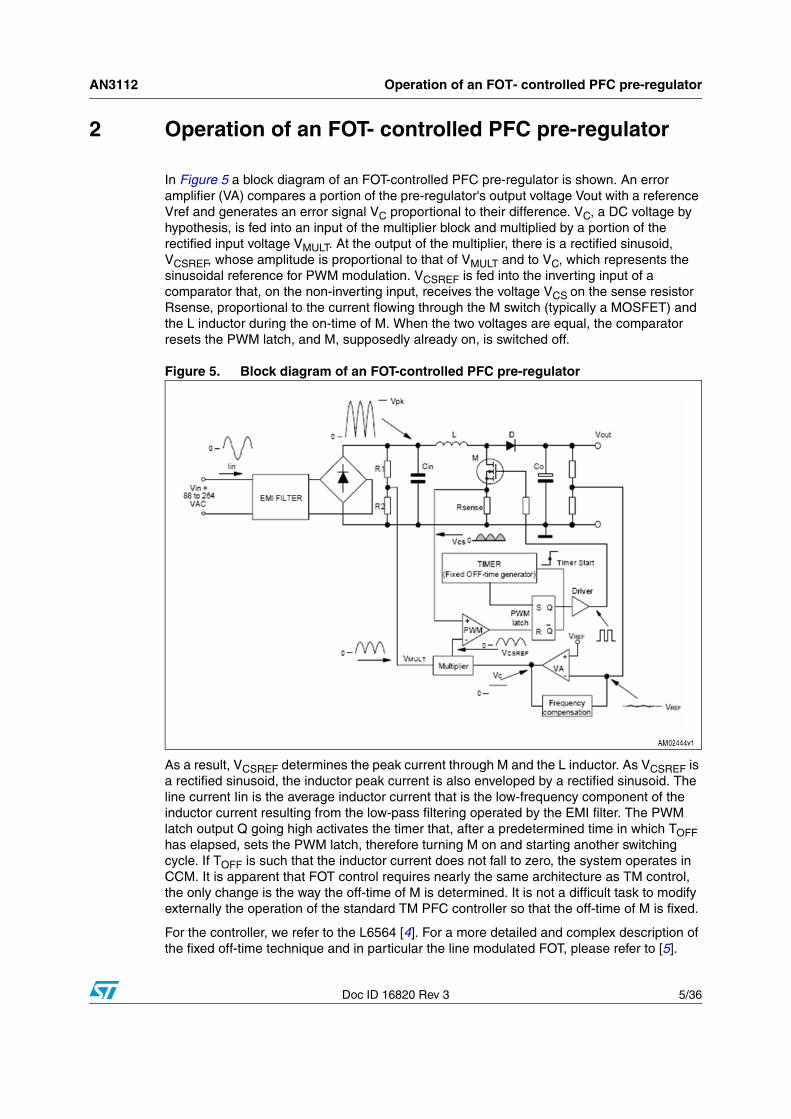
2 Operation of an FOT- controlled PFC pre-regulator
In Figure 5 a block diagram of an FOT-controlled PFC pre-regulator is shown. An error amplifier (VA) compares a portion of the pre-regulator's output voltage Vout with a reference Vref and generates an error signal VC proportional to their difference. VC, a DC voltage by hypothesis, is fed into an input of the multiplier block and multiplied by a portion of the rectified input voltage VMULT. At the output of the multiplier, there is a rectified sinusoid, VCSREF, whose amplitude is proportional to that of VMULT and to VC, which represents the sinusoidal reference for PWM modulation. VCSREF is fed into the inverting input of a comparator that, on the non-inverting input, receives the voltage VCS on the sense resistor Rsense, proportional to the current flowing through the M switch (typically a MOSFET) and the L inductor during the on-time of M. When the two voltages are equal, the comparator resets the PWM latch, and M, supposedly already on, is switched off.
Figure 5. Block diagram of an FOT-controlled PFC pre-regulator
As a result, VCSREF determines the peak current through M and the L inductor. As VCSREF is a rectified sinusoid, the inductor peak current is also enveloped by a rectified sinusoid. The line current Iin is the average inductor current that is the low-frequency component of the inductor current resulting from the low-pass filtering operated by the EMI filter. The PWM latch output Q going high activates the timer that, after a predetermined time in which TOFF has elapsed, sets the PWM latch, therefore turning M on and starting another switching cycle. If TOFF is such that the inductor current does not fall to zero, the system operates in CCM. It is apparent that FOT control requires nearly the same architecture as TM control, the only change is the way the off-time of M is determined. It is not a difficult task to modify externally the operation of the standard TM PFC controller so that the off-time of M is fixed.
For the controller, we refer to the L6564 [4]. For a more detailed and complex description of the fixed off-time technique and in particular the line modulated FOT, please refer to [5].
Implementing the line-modulated fixed-off-time AN3112
6/36 Doc ID 16820 Rev 3
3 Implementing the line-modulated fixed-off-time
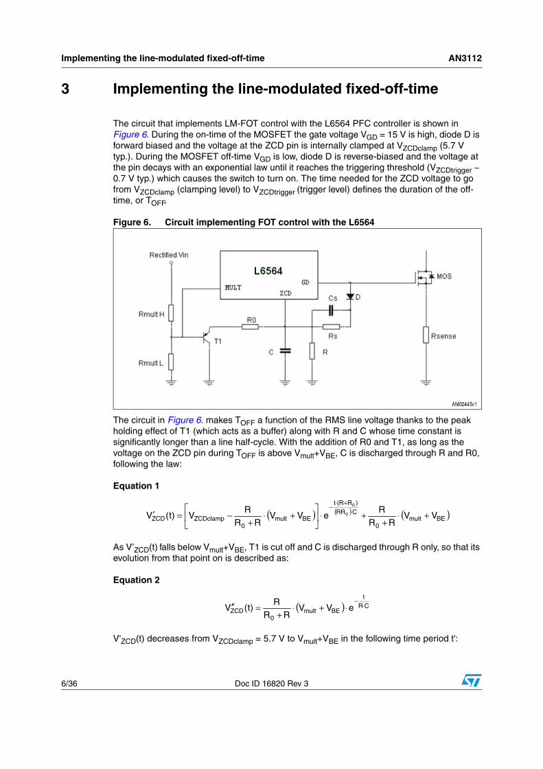
The circuit that implements LM-FOT control with the L6564 PFC controller is shown in Figure 6. During the on-time of the MOSFET the gate voltage VGD = 15 V is high, diode D is forward biased and the voltage at the ZCD pin is internally clamped at VZCDclamp (5.7 V typ.). During the MOSFET off-time VGD is low, diode D is reverse-biased and the voltage at the pin decays with an exponential law until it reaches the triggering threshold (VZCDtrigger ~ 0.7 V typ.) which causes the switch to turn on. The time needed for the ZCD voltage to go from VZCDclamp (clamping level) to VZCDtrigger (trigger level) defines the duration of the off-time, or TOFF.
Figure 6. Circuit implementing FOT control with the L6564
The circuit in Figure 6. makes TOFF a function of the RMS line voltage thanks to the peak holding effect of T1 (which acts as a buffer) along with R and C whose time constant is significantly longer than a line half-cycle. With the addition of R0 and T1, as long as the voltage on the ZCD pin during TOFF is above Vmult+VBE, C is discharged through R and R0, following the law:
Equation 1
As V’ZCD(t) falls below Vmult+VBE, T1 is cut off and C is discharged through R only, so that its evolution from that point on is described as:
Equation 2
V'ZCD(t) decreases from VZCDclamp = 5.7 V to Vmult+VBE in the following time period t':
( ) ( ) ( )BEmult0
CRR)RR(t
BEmult0
ZCDclampZCD VVRR
ReVV
RRR
V)t(V 0
0
+⋅+
+⋅⎥⎦
⎤⎢⎣
⎡+⋅
+−=′ ⋅
+⋅−
( ) CRt
BEmult0
ZCD eVVRR
R)t(V ⋅
−⋅+⋅
+=′′

AN3112 Implementing the line-modulated fixed-off-time
Doc ID 16820 Rev 3 7/36
Equation 3
and V''ZCD(t) decreases from Vmult+VBE to VZCDtrigger = 0.7 V (trigger level) in the following time period t'':
Equation 4
Figure 7 illustrates the signal on the ZCD pin with the two discharging time constants depending on the two resistors R, R0 and the L6564 parameters, particularly the upper clamp voltage and the triggering voltage of the ZCD pin.
Figure 7. ZCD pin signal with the fixed off-time generator circuit
The sum of the two time periods is the off-time function:
Equation 5
In this way, once the multiplier operating point (that is, the Vmult /VAC ratio) is fixed, with the proper selection of R and R0, it is possible to increase TOFF with the line voltage so that, at maximum line voltage, it is always TON>TONmin, where TONmin is the minimum on-time of the L6564 gate drive [4]. This is a required condition in order to avoid line distortion [5].
( )( ) ⎥
⎥⎦
⎤
⎢⎢⎣
⎡⋅+−+⋅
⋅+⋅⋅
+⋅
−=′RVV)RR(V
RVVlnC
RRRR
tBEmult0ZCDclamp
0BEmult
0
0
⎥⎦
⎤⎢⎣
⎡+
⋅−=′′BEmult
ZCDtrigger
VV
VlnRCt
( )( ) ( ) ⎥
⎥⎦
⎤
⎢⎢⎣
⎡⎟⎟⎠
⎞⎜⎜⎝
⎛+
+⎥⎥⎦
⎤
⎢⎢⎣
⎡
⋅+−+⋅⋅+
⋅+
⋅−=BEmult
ZCDtrigger
BEmult0ZCDclamp
0BEmult
0
0OFF VV
Vln
RVV)RR(VRVV
lnRR
RRCT

Implementing the line-modulated fixed-off-time AN3112
8/36 Doc ID 16820 Rev 3
It is easy to see that TOFF is now a function of the instantaneous line voltage. We refer to this technique as line-modulated fixed-off-time (LM-FOT) [5].
This modification, although simple, introduces profound changes in the timing relationships, with a positive influence on the energetic relationships. From the control point of view, modulating TOFF is a feed-forward term that modifies the gain but does not change its characteristics. Consequently, all of the properties of the standard FOT control are maintained. Due to the highly non-linear nature of the TOFF modulation introduced by T1 and R0, its effects are discussed only qualitatively and the quantitative aspects are provided graphically for a specific case in [5].
As a practical rule, it is convenient to first select a capacitor and then to calculate the resistor needed to achieve the desired TOFF (see Section 4.3.7 on page 19).
As the gate voltage VGD rises, the Rs resistor charges the C timing capacitor as quickly as possible up to VZCDclamp, without exceeding the clamp rating (IZCDx =10 mA). Then it must fulfill the following inequalities:
Equation 6
where VGD (assume VGD = 10 V) is the voltage delivered by the gate driver, VGDx = 15 V its maximum value, and VF the forward drop on D.
When working at high line/light load the on-time of the power switch becomes very short and the Rs resistor alone is no longer able to charge C up to VZCDclamp. The speed-up capacitor Cs is then used in parallel to Rs. This capacitor causes an almost instantaneous charge of C up to a certain level, after that, Rs completes the charge up to VZCDclamp. It is important that the steep edge caused by Cs does not reach the clamp level, otherwise the internal clamp of the L6564 undergoes uncontrolled current spikes (limited only by the dynamic resistance of the 1N4148 and the ESR of Cs) that could overstress the IC. Cs must then be:
Equation 7
ZCDclamp
FZCDclampGD
ZCDclampZCDx
FZCDclampGDx
V
VVVRRs
R
VI
VVV −−⋅<<
+
−−
FZCDclampGDx
ZCDclamp
VVV
VCCs
−−<
AN3112 Designing a fixed-off-time PFC
Doc ID 16820 Rev 3 9/36
4 Designing a fixed-off-time PFC
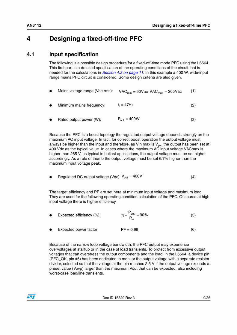
4.1 Input specificationThe following is a possible design procedure for a fixed-off-time mode PFC using the L6564. This first part is a detailed specification of the operating conditions of the circuit that is needed for the calculations in Section 4.2 on page 11. In this example a 400 W, wide-input range mains PFC circuit is considered. Some design criteria are also given.
Because the PFC is a boost topology the regulated output voltage depends strongly on the maximum AC input voltage. In fact, for correct boost operation the output voltage must always be higher than the input and therefore, as Vin max is Vpk, the output has been set at 400 Vdc as the typical value. In cases where the maximum AC input voltage VACmax is higher than 265 V, as typical in ballast applications, the output voltage must be set higher accordingly. As a rule of thumb the output voltage must be set 6/7% higher than the maximum input voltage peak.
The target efficiency and PF are set here at minimum input voltage and maximum load. They are used for the following operating condition calculation of the PFC. Of course at high input voltage there is higher efficiency.
Because of the narrow loop voltage bandwidth, the PFC output may experience overvoltages at startup or in the case of load transients. To protect from excessive output voltages that can overstress the output components and the load, in the L6564, a device pin (PFC_OK, pin #6) has been dedicated to monitor the output voltage with a separate resistor divider, selected so that the voltage at the pin reaches 2.5 V if the output voltage exceeds a preset value (Vovp) larger than the maximum Vout that can be expected, also including worst-case load/line transients.
Mains voltage range (Vac rms): (1)
Minimum mains frequency: (2)
Rated output power (W): (3)
Regulated DC output voltage (Vdc) (4)
Expected efficiency (%): (5)
Expected power factor: (6)
Vac90VACmin = Vac265VACmax =
Hz47fl =
W400Pout =
V400Vout =
%90P
P
in
out ==η
99.0PF =
Designing a fixed-off-time PFC AN3112
10/36 Doc ID 16820 Rev 3
The mains frequency generates a 2fL voltage ripple on the output voltage at full load. The ripple amplitude determines the current flowing into the output capacitor and the ESR. Additionally, a certain hold-up capability in case of mains dips can be requested from the PFC in which case the output capacitor must also be dimensioned, taking into account the required minimum voltage value (Vout min) after the elapsed hold-up time (tHold).
The PFC minimum switching frequency is one of the main parameters used to dimension the boost inductor. Here we consider the switching frequency at low mains on top of the sinusoid and at full load conditions. As a rule of thumb, it must be higher than the audio bandwidth in order to avoid audible noise and additionally it must not interfere with the L6564 minimum internal starter period, as given in the datasheet. Alternatively, if the minimum frequency is set too high the circuit shows excessive losses at higher input voltage and probably operates skipping switching cycles not only at light load. The typical minimum frequency range is 55÷95 kHz for wide range operation.
The design is done on the basis of a ripple factor (the ratio of the maximum current ripple amplitude to the inductor peak current at minimum line voltage) kr=0.34.
In order to properly select the power components of the PFC and dimension the heat sinks in case they are needed, the maximum operating ambient temperature around the PFC circuit must be known. Please note that this is not the maximum external operating temperature of the entire equipment, but it is the local temperature at which the PFC components are working.
Maximum. output voltage (Vdc): (7)
Maximum output low frequency ripple: (8)
Minimum output voltage after line drop (Vdc): (9)
Hold-up capability (ms):
(10)
Minimum switching frequency (kHz) (11)
Ripple factor (12)
Maximum ambient temperature (°C): (13)
V430VOVP =
V10Vout =∆
V300V minout =
ms20tHold =
kHz80f minsw =
34.0kr =
C50Tambx °=

AN3112 Designing a fixed-off-time PFC
Doc ID 16820 Rev 3 11/36
4.2 Operating conditionThe first step is to define the main parameters of the circuit, using the specification points given in Section 4.1 on page 9:
Rated DC output current:
Equation 8
Maximum input power:
Equation 9
Referring to the main currents shown in Figure 1, the following formula expresses the maximum value of current circulating in the boost cell which means at minimum line voltage of the selected range:
RMS input current:
Equation 10
It is important to define the following ratios in order to continue describing the energetic relationships in the PFC:
Equation 11
Equation 12
From Equation 11 and Equation 12:
Line peak current:
Equation 13
Inductor Ripple-∆ILpk:
out
outout V
PI = A00.1
V400W400
Iout ==
η= out
inP
P W44.44410090
W400Pin =⋅=
PFVAC
PI
min
outin ⋅
= A99.499.0Vac90
W400Iin =
⋅=
out
minmin V
VAC2k = 32.0
V400Vac90
2kmin ==
out
maxmax V
VAC2k = 94.0
V400Vac265
2kmax ==
outmin
inmaxPK Vk
P2I
⋅⋅= A98.6
V40032.0W44.4442
I maxPK =⋅
⋅=

Designing a fixed-off-time PFC AN3112
12/36 Doc ID 16820 Rev 3
Equation 14
Inductor peak current:
Equation 15
It is also possible to calculate the RMS current flowing into the switch and into the diode, needed to calculate the losses of these two elements.
RMS switch current:
Equation 16
RMS diode current:
Equation 17
It is worth remembering that the accuracy of the approximate energetic relationships described here is quite good at maximum load for low values of parameter k, that is, at low line voltage, but worsens at high line and as the power throughput is reduced. Since, in the design phase, current stress is calculated at maximum load and minimum line voltage, their accuracy is acceptable for design purposes.
4.3 Power section design
4.3.1 Bridge rectifier
The input rectifier bridge can use standard slow recovery, low-cost devices.
Typically a 600 V device is selected in order to obtain a good margin against mains surges. An NTC resistor, limiting the current at turn-on, is required to avoid overstress to the diode bridge.
The rectifier bridge power dissipation can be calculated using equationsEquation 18,Equation 19,Equation 20. The threshold voltage (Vth) and dynamic resistance (Rdiode) of a single diode bridge can be found in the component datasheet.
maxPKr
rpk I
k38k6
IL ⋅⋅−
⋅=∆ A04.2A98.634.038
34.06ILpk =⋅
⋅−⋅=∆
maxPKr
maxpk Ik38
8IL ⋅
⋅−= A01.8A98.6
34.0388
IL maxpk =⋅⋅−
=
π⋅
−⋅⋅
=3k16
2Vk
PISW min
outmin
inrms A22.4
332.016
2V40032.0
W400ISWrms =
π⋅−⋅
⋅=
π⋅
⋅=
3k16
VkP
ID min
outmin
inrms A57.2
332.016
V40032.0W400
IDrms =π
⋅⋅⋅
=

AN3112 Designing a fixed-off-time PFC
Doc ID 16820 Rev 3 13/36
Equation 18
Equation 19
The power dissipated on a D15XB60 bridge may be:
Equation 20
4.3.2 Input capacitor
The input filter capacitor (Cin) is placed across the diode bridge output. This capacitor must smooth the high-frequency ripple and must sustain the maximum instantaneous input voltage. In a typical application an EMI filter is placed between the mains and the PFC circuit. In this application the EMI filter is reinforced by a differential mode Pi-filter after the bridge to reject the differential noise coming from the whole switching circuit. The design of the EMI filter (common mode and differential mode) is not described here. The value of the input filter capacitor can be calculated as follows, simply considering the output power that the PFC should deliver at full load:
Equation 21
The maximum value of this capacitor is limited to avoid line current distortion. The value
chosen for this design is 1 µF.
4.3.3 Output capacitor
The output bulk capacitor (Co) selection depends on the DC output voltage (4), the allowed maximum voltage (7) and the converter output power (3).
The 100/120 Hz (twice the mains frequency) voltage ripple (Vout = peak-to-peak ripple value) (8) is a function of the capacitor impedance and the peak capacitor current:
Equation 22
With a low ESR capacitor the capacitive reactance is dominant, therefore:
A53.32
A99.422
I2I ininrms =⋅=⋅=
A25.2A99.42I2
I inavg_in =
π⋅=
π⋅
=
avg_inthinrms2
diodebridge IV4IR4P ⋅⋅+⋅⋅=
W53.7A25.2V7.04)A53.3(025.04P 2bridge =⋅⋅+⋅Ω⋅=
out3
in P105.2C ⋅⋅= − F1W400105.2C 3in µ=⋅⋅= −
22
Oloutout ESR
)Cf22(
1I2V +
⋅⋅π⋅⋅=∆
Designing a fixed-off-time PFC AN3112
14/36 Doc ID 16820 Rev 3
Equation 23
Vout is usually selected in the range of 1.5% of the output voltage. Although ESR does not usually affect the output ripple, it should be taken into account for power loss calculations. The total RMS capacitor ripple current, including mains frequency and switching frequency components, is:
Equation 24
If the PFC stage must guarantee a specified hold-up time, the selection criterion of the capacitance is different. Co has to deliver the output power for a certain time (tHold) with a specified maximum dropout voltage (Vout min) that is the minimum output voltage value (which takes load regulation and output ripple into account). Vout min is the minimum output operating voltage before the 'power fail' detection and consequent stopping by the downstream system supplied by the PFC.
Equation 25
A 20% tolerance on the electrolytic capacitors must be taken into account for correct dimensioning.
Following the previous relationships, after selecting the commercial value of 330 µF the actual hold-up capability and ripple voltage are recalculated.
In detail:
Equation 26
Equation 27
4.3.4 Boost inductor
In the continuous mode approach, the acceptable current ripple factor, Kr, is typically fixed in the range between 10% to 35%. For this design, the maximum specified current ripple factor is 34%.
outoutl
out
outl
outO VVf2
P
Vf2
IC
∆⋅⋅⋅π=
∆⋅⋅π≥ F338
V10V400Hz472W400
CO µ=⋅⋅⋅π
≥
2outrms
2Crms IIDI −= ( ) ( ) A36.2A0.1A56.2I 22
Crms =−=
( ) 2minout
2outout
HoldoutO
VVV
tP2C
−∆−
⋅⋅=
( ) ( )F3.242
V300V10V400
ms20W4002C
22O µ=−−
⋅⋅=
( )out
2minout
2outoutO
hold P2
VVVCt
⋅⎥⎦⎤
⎢⎣⎡ −∆−⋅
=( ) ( )[ ]
ms22W4002
V300V10V400F330t
22
hold =⋅
−−⋅µ=
Ol
outout Cf2
IV
⋅⋅π⋅=∆ V2.10
F330Hz472A0.1
Vout =µ⋅⋅π⋅
=∆

AN3112 Designing a fixed-off-time PFC
Doc ID 16820 Rev 3 15/36
To calculate the required inductance L of the boost inductor, use the following formula with a 3.76 µs off-time set at 90 Vac (see the following ZCD pin dimensioning to find the meaning of this value):
Equation 28
After calculating the inductor value at low mains and at high mains L(VACmax), L(VACmin) (Equation 28) depending also on the off-time, the minimum value must be taken into account. It becomes the maximum inductance value for the PFC dimensioning.
Figure 8 shows the switching frequency versus the θ angle calculated inverting Equation 28 with a 500 µH boost inductance and fixing the line voltage at minimum and maximum values.
Figure 8. Switching frequency fixing the line voltage
)VAC(TIL
V)k1()VAC(L OFF
pk
outmin ∆
⋅−= H501s76.3A04.2V400
)32.01()VAC(L min µ=µ⋅−=
Frequency modulation with the Line half period
1
10
100
1000
0 0.4 0.8 1.2 1.6 2 2.4 2.8÷ [Line half period]
kHz
Switching Freq.@VacMin
Switching Freq.@VacMax
CCM
DCM DCM
TM TM
θ1 θ2
θ

Designing a fixed-off-time PFC AN3112
16/36 Doc ID 16820 Rev 3
Figure 9. The effect of fixing off-time - boundary between DCM and CCM
The effect of fixing the off-time is to generate a continuous conduction mode in the center region of the line half-cycle between the two transition angles. Close to the zero-crossing, the system works in discontinuous conduction mode and in transition mode at the boundary.
The inductor core size is determined assuming a peak flux density Bx ~0.25 T (depending on the ferrite grade selected and relevant specific losses) and calculating the maximum current according to Equation 15 as a function of the maximum current sense pin clamping voltage and sense resistor value.
DC and AC copper losses and ferrite losses must also be calculated to determine the maximum temperature rise of the inductor.
4.3.5 Power MOSFET selection and power dissipation calculation
The selection of the MOSFET concerns mainly its RDS(on), basically proportional to the output power. The MOSFET breakdown voltage is selected considering the PFC nominal output voltage (4) adding some margin (20%) to guarantee reliable operation.
Therefore, a voltage rating of 500 V (1.2 · Vout = 480 V) is selected. Using its current rating as a rule of thumb, we can select a device having ~ 3 times the RMS switch current (Equation 16) but, the power dissipation calculation gives the final confirmation that the selected device is the right one for the circuit, also taking the heat sink dimensions into account. For example, in a 400 W PFC application two parallel STP12NM50FP MOSFETs can be selected.
The MOSFET's power dissipation depends on conduction, switching and capacitive losses.
The conduction losses at maximum load and minimum input voltage are calculated by:
Equation 29
Because, normally in the datasheets the RDS(on) is given at an ambient temperature (25 °C), to correctly calculate the conduction losses at 100°C (typical MOSFET junction operating
DCM
TM
CCM
TOFF
θ 1
Half Line Cycle
DCM
TM
CCM
TOFF
θ 1
Half Line Cycle
( )2rmsoncond )VAC(ISWRDS)VAC(P ⋅=
AN3112 Designing a fixed-off-time PFC
Doc ID 16820 Rev 3 17/36
temperature), a factor of 1.75 to 2 should be taken into account. The exact factor can be found on the device datasheet.
Now, combining equations Equation 29 and Equation 16, the conduction losses referred to a 1 ΩRDS(on), at ambient temperature as a function of Pin and VAC can be calculated:
Equation 30
The generic switching losses due to the MOSFET commutation occurring at turn-on and turn-off can be basically expressed by:
Equation 31
Because the switching frequency depends on the input line voltage and phase angle on the sinusoidal waveform, it can be demonstrated that from Equation 31 the switching losses per 1 µs of current, rise and fall-time can be written as:
Equation 32
From the STP12NM50FP datasheet trise = tfall = 0.01 µs is the crossover time at turn-on and off.
At turn-on the losses are due to the discharge of the total drain capacitance inside the MOSFET itself. In general, the capacitive losses are given by:
Equation 33
Where Cd is the total drain capacitance including the MOSFET and the other parasitic capacitances such as inductor etc. At the drain node, VMOS is the drain voltage at MOSFET turn-on.
Taking into account the frequency variation with the input line voltage and the phase angle, the capacitive losses per 1 nF of total drain capacitance can be calculated as:
Equation 34
The total drain capacitance (Cd) of the two parallel MOSFETs is 0.36 nF, not including the other component contributions, Vout is the drain voltage at MOSFET turn-on.
2
out
in2rmscond 3
)VAC(k162
V)VAC(kP
2))VAC(ISW(2)VAC(P ⎟⎟⎠
⎞⎜⎜⎝
⎛
π⋅−⋅
⋅⋅=⋅=′
)VAC(f2
ttIV)VAC(P sw
fallriseMOSMOSswitch ⋅⎟
⎠⎞⎜
⎝⎛ +
⋅⋅=
( )∫π
ϑ⋅θ⋅ϑπ
⋅⎟⎟⎠
⎞⎜⎜⎝
⎛ ∆−⋅=′
0
sw2pk
maxpkoutswitch d),VAC(fsin1
2
ILILV)VAC(P
)VAC(fVC21
)VAC(P swMOS2
dcap ⋅⋅⋅=
( ) ϑ⋅ϑπ
⋅=′ ∫π
d),VAC(fV1
21
)VAC(P0
sw2
outcap
Designing a fixed-off-time PFC AN3112
18/36 Doc ID 16820 Rev 3
The MOSFET total losses as a function of the input mains voltage is the sum of the three previous losses from Equation 30, Equation 32, and Equation 34, multiplied for relevant MOSFET parameters:
Equation 35
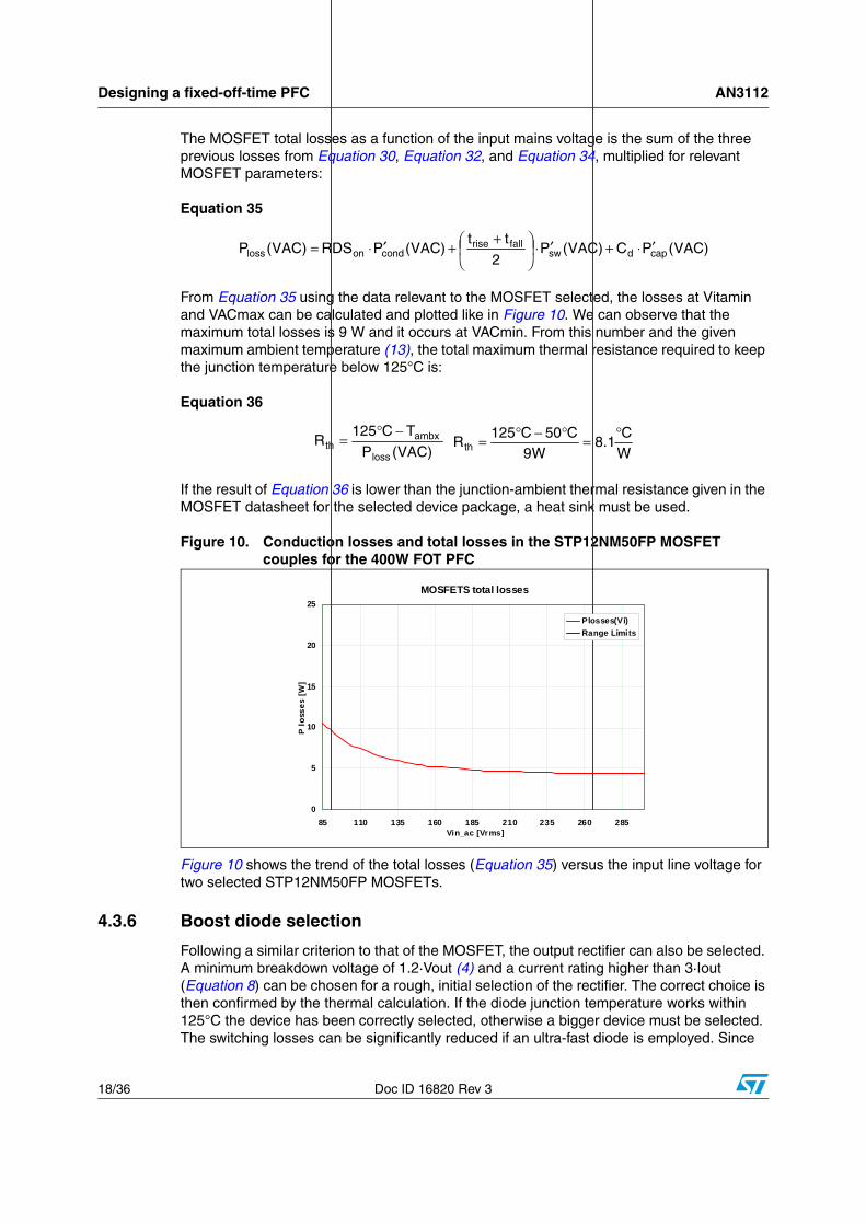
From Equation 35 using the data relevant to the MOSFET selected, the losses at Vitamin and VACmax can be calculated and plotted like in Figure 10. We can observe that the maximum total losses is 9 W and it occurs at VACmin. From this number and the given maximum ambient temperature (13), the total maximum thermal resistance required to keep the junction temperature below 125°C is:
Equation 36
If the result of Equation 36 is lower than the junction-ambient thermal resistance given in the MOSFET datasheet for the selected device package, a heat sink must be used.
Figure 10. Conduction losses and total losses in the STP12NM50FP MOSFET couples for the 400W FOT PFC
Figure 10 shows the trend of the total losses (Equation 35) versus the input line voltage for two selected STP12NM50FP MOSFETs.
4.3.6 Boost diode selection
Following a similar criterion to that of the MOSFET, the output rectifier can also be selected. A minimum breakdown voltage of 1.2·Vout (4) and a current rating higher than 3·Iout (Equation 8) can be chosen for a rough, initial selection of the rectifier. The correct choice is then confirmed by the thermal calculation. If the diode junction temperature works within 125°C the device has been correctly selected, otherwise a bigger device must be selected. The switching losses can be significantly reduced if an ultra-fast diode is employed. Since
)VAC(PC)VAC(P2
tt)VAC(PRDS)VAC(P capdsw
fallrisecondonloss ′⋅+′⋅⎟
⎠⎞⎜
⎝⎛ +
+′⋅=
)VAC(P
TC125R
loss
ambxth
−°=
WC
1.8W9
C50C125Rth
°=°−°=
MOSFETS total losses
0
5
10
15
20
25
85 110 135 160 185 210 235 260 285Vin_ac [Vrms]
P lo
sses
[W
]
Plosses(Vi)Range Limits

AN3112 Designing a fixed-off-time PFC
Doc ID 16820 Rev 3 19/36
this circuit operates in the continuous current mode, the MOSFET has to recover the boost diode minority carrier charge at turn-on. Therefore, an ultrafast or a SiC rectifier must be selected.
In this 400 W application an STTH8R06 (600 V, 8 A) can be selected. The STTH8R06 offers the best solution for the continuous current mode operation due to its very fast reverse recovery time, typically 25 ns. This part has a breakdown voltage rating (Vrrm) of 600 V, average forward current rating (Ifave) of 8 A and reverse recovery time (trr) of 25 ns. The rectifier AVG (Equation 8) and RMS (Equation 17) current values and the parameter Vth (rectifier threshold voltage) and Rd (dynamic resistance) given in the datasheet allow the calculation of the rectifier losses.
From the STTH8R06 datasheet, Vth is 1.16 V, Rd is 0.08 Ω, neglecting the recovery losses:
Equation 37
From (13) and Equation 37 the maximum thermal resistance to keep the junction temperature below 125°C is then:
Equation 38
4.3.7 L6564 biasing circuitry
Following the dimensioning of the power components, the biasing circuitry for the L6564 is also described here. For reference, the internal schematic of the L6564 is represented in Figure 11. For more detail on the internal functions please refer to the datasheet.
Figure 11. L6564 internal schematic
rms2
doutthdiode IDRIVP ⋅+⋅= ( ) W69.1A56.208.0A0.1V16.1P 2diode =⋅Ω+⋅=
diode
ambxth P
TC125R
−°=
WC
45.44W69.1
C50C125Rth
°=°−°=
Designing a fixed-off-time PFC AN3112
20/36 Doc ID 16820 Rev 3
Pin 1 (INV) is connected both to the inverting input of the E/A and to the OVP circuitry. A resistive divider is connected between the boost regulated output voltage and this pin. The internal reference on the non-inverting input of the E/A is 2.5 V (typ.), the output voltage (Vout) of the PFC pre-regulator is set at its nominal value, by the resistors ratio of the feedback output divider. RoutH and RoutL are then selected considering the desired nominal output voltage and the desired output power dissipated on the output divider. For example for a 50 mW output divider dissipation:
Equation 39
With the commercial value selected RoutH = 3 MΩ:
Equation 40
Equation 41
RoutL = 62 kΩ in parallel to a 27 kΩ can be selected. Please note that for RoutH a resistor with a suitable voltage rating (>400 V) is needed, or more resistors in series must be used.
Pin 6 (PFC_OK - feedback failure protection): The PFC_OK pin is dedicated to monitoring the output voltage with a separate resistor divider. This divider is selected so that the voltage at the pin reaches 2.5 V if the output voltage exceeds a preset value (Vovp), usually larger than the maximum Vout that can be expected, also including worst-case load/line transients. For a maximum output voltage Vout max of 430 V and selecting a 50 µA current flowing into the divider:
Equation 42
By selecting a commercial value of 51kΩ:
Equation 43
Connecting in series, two 3.3 MΩ resistors and one 2.2 MΩ resistor, a total value of 8.8 MΩ can be obtained.
Note that both feedback dividers connected to the L6564 pin #1 (INV) and pin #6 (PFC_OK) can be selected without any constraints. The unique criterion is that both dividers must sink
mW50
)V5.2V(R
2OUT
outH−
= Ω=−= M160.3mW50
)V5.2V400(R
2
outH
1V5.2
V
R
R out
outL
outH −= 1591V5.2V400
R
R
outL
outH =−=
159R
R outHoutL = Ω=Ω= k8.18
159M3
RoutL
divider
OK_PFC_REFL I
VR = Ω=
µ= k50
A50
V5.2RL
⎟⎟⎠
⎞⎜⎜⎝
⎛−⋅= 1
V
VRR
OK_PFC_REF
MAX_OUTLH Ω=⎟
⎠⎞⎜
⎝⎛ −⋅Ω= M721.81
V5.2V430
k51RH
AN3112 Designing a fixed-off-time PFC
Doc ID 16820 Rev 3 21/36
a current from the output bus which needs to be significantly higher than the current biasing the error amplifier and PFC_OK comparator.
The OVP function described above can handle "normal" over-voltage conditions, that is, those resulting from an abrupt load/line change or occurring at start-up. If the over-voltage is generated by a feedback disconnection for instance, when one of the upper resistors of the output divider fails to open, an additional circuitry detects the voltage drop of pin INV. If the voltage on pin INV is lower than 1.66V (Typ.) and at same time the OVP is active, a feedback failure is assumed.
Therefore, the gate drive activity is immediately stopped, the device is shut down, its quiescent consumption is reduced to below 180 µA and the condition is latched as long as the supply voltage of the IC is above the UVLO threshold. To restart the system it is necessary to recycle the input power, so that the Vcc voltage of the L6564 goes below 6 V and that one of the PWM controllers goes below its UVLO threshold. Note that this function offers complete protection against feedback loop failures or erroneous settings, and also against the failure of the protection itself. Either resistor of the PFC_OK divider failing short or open or a PFC_OK pin floating may result in shutting down the IC and stopping the pre-regulator. In addition, the PFC_OK pin doubles its function as a not-latched IC disable: a voltage below 0.23 V shuts down the IC, reducing its consumption below 2 mA. To restart the IC, simply let the voltage at the pin go above 0.27 V.
Pin 2 (COMP): This pin is the output of the E/A that is fed into one of the two inputs of the multiplier. A feedback compensation network is placed between this pin and the INV pin (pin#1). It must be designed with a narrow bandwidth in order to avoid the system rejecting the output voltage ripple (100 Hz) that would cause high distortion of the input current waveform. A theoretical criterion to define the compensation network value is to set the E/A bandwidth (BW) from 20 to 30 Hz.
For a more complex way of compensating the FOT PFC please refer to [1], [2], [3].
A compensated two-pole feedback network for this 400 W FOT PFC can be obtained with the following values:
to which the following open-loop transfer function and its phase function correspond.
nF100CcompP = F1CcompS µ= Ω= k56RcompS (14)
Designing a fixed-off-time PFC AN3112
22/36 Doc ID 16820 Rev 3
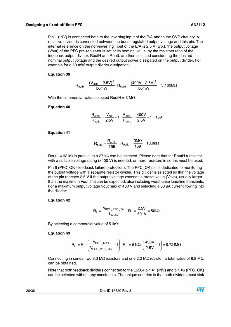
The two bode plot charts are relevant to the PFC operating at the main voltage set point of 265 Vac and full load. In this condition the crossover frequency is fc = 4 Hz, the phase margin is 50° and the third harmonic distortion is below 3%.
Pin 4 (CS): The #4 pin is the inverting input of the current sense comparator. Through this pin, the L6564 senses the instantaneous inductor current, converted in a proportional voltage by an external sensing resistor (Rs). As this signal crosses the threshold set by the multiplier output, the PWM latch is reset and the power MOSFET is turned off. The MOSFET stays in off-state until the PWM latch is set again by the ZCD signal. The pin is equipped with 150 ns (typ.) leading-edge blanking for improved noise immunity.
The sense resistor value (Rs) can be calculated as follows. For the 400 W PFC it is:
Equation 44
Where:
ILpk: it is the maximum peak current in the inductor, calculated as described in 4.2
Vcsmin = 1.0 V, it is the minimum voltage admitted on the L6564 current sense (on the datasheet).
Because the internal current sense clamping sets the maximum current that can flow in the inductor, the maximum peak of the inductor current may be calculated considering the maximum voltage Vcsmax allowed on the L6564 (on datasheet):
Equation 45
The calculated ILpkx is the value at which the boost inductor must not be in saturation and it is used for calculating the inductor number of turns and air-gap length.
Figure 12. Open loop transfer function-bode plot
Figure 13. Phase
-200
-100
0
100
0.1 1 10 100 1000f [Hz]
Gain
[dB]
-200
-150
-100
0.1 1 10 100 1000f [Hz]
Phas
e [d
eg]
maxpk
mins IL
VcsR < Ω=< 124.0
A01.8V0.1
Rs
s
maxpksat R
VcsIL = A67.9
12.0V16.1
ILpksat =Ω
=

AN3112 Designing a fixed-off-time PFC
Doc ID 16820 Rev 3 23/36
The power dissipated by Rs is given by:
Equation 46
According to the result, for example four parallel resistors of 0.47 Ω with 1 W of power rating can be selected.
Pin 3 (MULT): The MULT pin is the second multiplier input. It is connected, through a resistive divider, to the rectified mains to obtain a sinusoidal voltage reference. The multiplier is described by the relationship:
Equation 47
Where:
VCS (Multiplier output) is the reference for the current sense (VCS_OFFSET is its offset).
k = 0.45 (Typ.) is the multiplier gain.
VCOMP is the voltage on pin 2 (E/A output).
VMULT is the voltage on pin 3.VFF is the second input to the multiplier for 1/V^2 function. It compensates the control loop gain dependence on the mains voltage. The voltage at this pin is a DC level equal to the peak voltage on the MULT pin (#3).
A complete description is given in the diagram in Figure 14 and Figure 15 which shows the typical multiplier characteristics family. The linear operation of the multiplier is guaranteed within the range 0 to 3 V of VMULT and the range 0 to 1.16 V (typ.) of Vcs, while the minimum guaranteed value of the maximum slope of the characteristics family (typ.) is:
2rmsss ISWRP ⋅= ( ) W14.222.412.0P 2
s =⋅Ω=
2FF
MULTCOMPmOFFSET_CSCS
V
V)V5.2V(kVV
⋅−⋅+=
Figure 14. Multiplier characteristics family for VFF =1 V
Figure 15. Multiplier characteristics family for VFF=3 V

Designing a fixed-off-time PFC AN3112
24/36 Doc ID 16820 Rev 3
Equation 48
The voltage on the MULT pin is also used to derive the information from the RMS mains voltage for the VFF compensation.
Before describing the correct operating point of the multiplier for the brownout function the voltage feed forward pin and its enable-disable property is here described:
Pin 5 (voltage feed forward): The power stage gain of PFC pre-regulators varies with the square of the RMS input voltage. As does the crossover frequency (fc) of the overall open-loop gain because the gain has a single pole characteristic. This leads to large trade-offs in the design. For example, setting the gain of the error amplifier to get fc = 20 Hz @ 264 Vac means having fc about 4 Hz @ 88 Vac, resulting in sluggish control dynamics. Additionally, the slow control loop causes large transient current flow during rapid line or load changes that are limited by the dynamics of the multiplier output. This limit is considered when selecting the sense resistor to let the full load power pass under minimum line voltage conditions, with some margin. But a fixed current limit allows excessive power input at high line, whereas a fixed power limit requires the current limit to vary inversely with the line voltage.
Voltage feed-forward can compensate for the gain variation with the line voltage and allow the overcoming of all of the above-mentioned issues. It consists of deriving a voltage proportional to the input RMS voltage, feeding this voltage into a squarer/divider circuit (1/V2 corrector) and providing the resulting signal to the multiplier which generates the current reference for the inner current control loop.
In this way, a change of the line voltage causes an inversely proportional change of the half-sine amplitude at the output of the multiplier (if the line voltage doubles the amplitude of the multiplier, output is halved and vice versa), so that the current reference is adapted to the new operating conditions with (ideally) no need for invoking the slow dynamics of the error amplifier. Additionally, the loop gain is constant throughout the input voltage range, which significantly improves the dynamic behavior at low line and simplifies loop design.
Actually, with another PFC embedding the voltage feed-forward, deriving a voltage proportional to the RMS line voltage implies a form of integration, which has its own time constant. If it is too small the voltage generated may be affected by a considerable amount of ripple at twice the mains frequency which causes distortion to the current reference (resulting in high THD and poor PF); if it is too large there may be a considerable delay in setting the right amount of feed-forward, resulting in excessive overshoot and undershoot of the pre-regulator's output voltage in response to large line voltage changes. Clearly a trade-off was required.
The L6564 produces an innovative voltage feed-forward which, with a technique that makes use of just two external parts, overcomes this time constant trade-off issue regardless of which voltage change occurs on the mains, both surges and drops. A capacitor CFF and a resistor RFF, both connected from the VFF pin (pin #5) to ground, complete an internal peak-holding circuit that provides a DC voltage equal to the peak of the rectified sine-wave applied on the MULT pin (pin #3). In this case the following value has been selected:
(15)
VV
66.1dV
dV
MULT
CS =
F1CFF µ= Ω= M1RFF
AN3112 Designing a fixed-off-time PFC
Doc ID 16820 Rev 3 25/36
In this way, in the case of a sudden line voltage rise, CFF is rapidly charged through the low impedance of the internal diode; in case of line voltage drop, an internal mains drop detector enables a low impedance switch which suddenly discharges CFF, avoiding long settling time before reaching the new voltage level. Consequently an acceptably low steady-state ripple and low current distortion can be achieved without any considerable undershoot or overshoot on the pre-regulator's output, like in systems with no feed-forward compensation This pin is internally connected to a comparator in order to provide the brownout (AC mains undervoltage) protection. A voltage below 0.8 V shuts down (not latched) the IC and brings its consumption to a considerably lower level. The IC restarts when the voltage at the pin rises above 0.88 V. These details must be taken into account during the MULT divider selection.
The suggested procedure to properly set the operating point of the multiplier is now described. First, the maximum peak value for VMULT, VMULTmax is selected. This value, which occurs at maximum mains voltage, should be 3 V or thereabouts in wide range mains and less in single mains. The sense resistor selected is Rs = 0.12 Ω and it is described in the pin 4 section. According to the L6564 datasheet and to the linearity setting of the pin, the maximum voltage on the multiplier input is:
From (16) the maximum required divider ratio is calculated as:
Equation 49
Supposing a 60 µA current flowing into the multiplier divider the lower resistor value can be calculated:
Equation 50
A commercial value of 51 kΩ for the lower resistor is selected. The upper resistor value can now be calculated:
Equation 51
In this example a RmultH = 6.9 MΩ and a RmultL = 51 kΩ can be selected. For RmultH a resistor with a suitable voltage rating (>400 V) is needed, or more resistors in series must be used.
The voltage on the multiplier pin with the selected component values re-calculated at minimum line voltage is 0.93 V and at maximum line voltage is 2.74 V. So the multiplier works correctly within its linear region.
(16)V3VMULTmax =
3
max
maxMULTp 108
Vac2652
V00.3
VAC2
Vk −⋅=
⋅=
⋅=
Ω=µ
=µ
= k50A60V00.3
A60
VR maxMULT
multL
Ω=Ω⋅
⋅−=−
= −
−M319.6k51
108
1081R
k
k1R
3
3
multLp
pmultH
Designing a fixed-off-time PFC AN3112
26/36 Doc ID 16820 Rev 3
Because the MULT divider also determines the mains input voltage at which the PFC starts and stops (brownout function), these values are calculated using the actual divider ratio:
Equation 52
And also the stop voltage:
Equation 53
Start and stop PFC mains voltage are compatible with the input mains voltage range (1).
In order to obtain the required startup and shutdown voltage, a reiteration may be required, by selecting MULT resistors and checking the actual PFC start and stop mains voltage.
Pin 7 (ZCD): This is the input of the zero current detector circuit. In FOT mode, it is connected to the line-modulated fixed-off-time circuit seen in Figure 6. Taking into account the information in Section 3: Implementing the line-modulated fixed-off-time, the starting point for the design of that circuit is the pair of the desired values for TOFF on the top of the line voltage sinusoid at minimum (TOFF @VACmin) and maximum line (TOFF @VACmax) obtained by setting the switching frequency on the peak of the sinusoid at low mains and considering the minimum on-time of the L6564:
Equation 54
Equation 55
Where Fswmin is the switching frequency on top of the sinusoid of the input voltage at VACmin = 90 Vac (Figure 16) and 220 ns is a corrector factor in order to consider the delay between the ZCD and GD signal.
Considering the ratio between Equation 55, Equation 54, we have:
Equation 56
In the formula, Equation 55 and Equation 54, the delay between the ZCD signal and the gate drive signal is taken into account in order to increase the accuracy of the mathematical model.
multL
multLmultHSTART R
RR
2
V88.0V
+⋅== V8.84
k51k51M9.6
2
V88.0VSTART =
ΩΩ+Ω⋅=
multL
multLmultHSTOP R
RR
2
V80.0V
+⋅== V1.77
k51k51M9.6
2
V80.0VSTOP =
ΩΩ+Ω⋅=
minsw
minminOFF f
k)VAC(T = s76.3ns220
kHz8032.0
)VAC(T minOFF µ=−=
max
maxminONmaxOFF k1
kT)VAC(T
−⋅
= s1.6ns22094.01
94.0ns450)VAC(T maxOFF µ=−
−⋅=
)VAC(T
)VAC(T
minOFF
maxOFFx =ρ 63.1
s76.3s1.6
x =µ
µ=ρ

AN3112 Designing a fixed-off-time PFC
Doc ID 16820 Rev 3 27/36
From the theory of the line modulation fixed off-time, TOFF increases with the line voltage so that at maximum line voltage the condition TON>TONmin [4] is always true. This is important in order to avoid line distortion [5].
Figure 16. Switching frequency function on the peak of the sinusoid input voltage waveform and the corresponding off- time value
Now considering the two discharging resistors R and R0 of the circuit in Figure 6, the ratio is defined as:
Equation 57
where 0 < K1 < 1. Through the definition of the k2 parameter the expected time constant τ =(R//R0)C is underlined, necessary for achieving the desired TOFF@90 Vac.
Equation 58
Finding a way to obtain K1 and K2 means to gain the values of R and R0 and the discharging time constant of the capacitor C.
The following section describes the mathematical way of obtaining the two parameters K1 and K2. Combining Equation 56, Equation 57, Equation 58 with the expression of the off-time (Equation 5), the following expressions are obtained:
RRR
K0
1 +=
τ=
)VAC(TK minOFF
2

Designing a fixed-off-time PFC AN3112
28/36 Doc ID 16820 Rev 3
Equation 59
Equation 60
From Equation 56 and Equation 59, solving the following equation:
Equation 61
And then substituting K1 value into the Equation 60 expression, the k2 parameters are obtained:
Equation 62
From the values of K1 and K2 it is possible to calculate the time constant τ =(R1//R2) C necessary to achieve the desired TOFF@90 Vac:
Equation 63
Now, by selecting a capacitor C in the hundred picofarad range or a few nanofarads, for example a C =220 pF, it is possible to determine the required equivalent resistance value:
Equation 64
From Equation 57 R and R0 are found:
[ ][ ][ ] ⎥
⎥
⎦
⎤
⎢⎢
⎣
⎡
⎟⎟⎠
⎞⎜⎜⎝
⎛+
+⎥⎥⎦
⎤
⎢⎢⎣
⎡⋅+−
−⋅+
⎥⎥⎥⎥⎥⎥
⎦
⎤
⎢⎢⎢⎢⎢⎢
⎣
⎡
⎟⎟⎟⎟
⎠
⎞
⎜⎜⎜⎜
⎝
⎛
+⋅+
⎥⎥⎥⎥⎥
⎦
⎤
⎢⎢⎢⎢⎢
⎣
⎡
⋅⎥⎥⎦
⎤
⎢⎢⎣
⎡⎥⎦
⎤⎢⎣
⎡+⋅−
−⋅⎥⎦
⎤⎢⎣
⎡+⋅
=ρ−
−
Fminmult
ZCDtriggerk1
1FminmultZCDclamp
1Fminmult
Fmin
maxminmult
ZCDtrigger
k1
1Fmin
maxminmultZCDclamp
1Fmin
maxminmult
1minmult
VV
Vln
)k(VVV)k1(VV
ln
VVACVAC
V
Vln
)k(VVACVAC
VV
)k1(VVACVAC
V
ln
)k,V(1
1
[ ][ ] ⎥
⎥
⎦
⎤
⎢⎢
⎣
⎡
⎟⎟⎠
⎞⎜⎜⎝
⎛+
+⎥⎥⎦
⎤
⎢⎢⎣
⎡
⋅+−−⋅+
⋅−−=
−
Fminmult
ZCDtriggerk1
1FminmultZCDclamp
1Fminmult
11minmult2 VV
Vln
kVVV
)k1(VVln
k11
)k,V(k1
0)k,V( x1minmult =ρ−ρ 903.0K1 =
)k,V(kK 1minmult22 = 17.11K2 =
2
minOFF
K
)VAC(T=τ ns35.336
17.11s76.3 =µ=τ
CReq
τ= Ω== k53.1pF220
ns35.336Req
AN3112 Designing a fixed-off-time PFC
Doc ID 16820 Rev 3 29/36
Equation 65
Equation 66
A commercial value R = 15 kΩ and a R0 = 1.5 kΩ has been chosen.
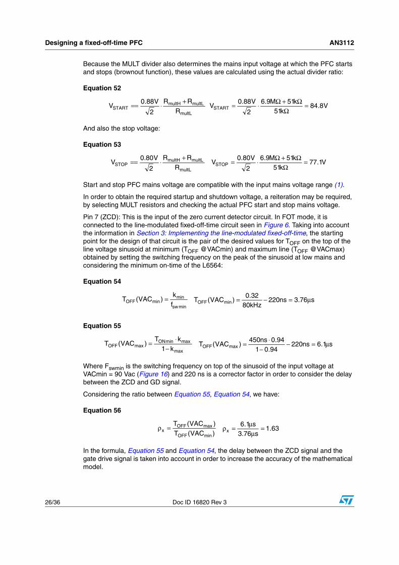
Figure 17 and Figure 18 show the trend of the off-time and the switching frequency vs the input mains voltage. The PFC inner current loop works in the range of 80 kHz-150 kHz.
Due to the tolerance of the capacitor selected (C) and the two discharging resistors, it is important to take into account a variation on the switching frequency in a real board of about ± 10%.
Finally the Rs limiting resistor should be selected according to the inequalities (Equation 6):
Equation 67
and the speed-up capacitor Cs using Equation 7.
Equation 68
This means that after calculations:
1
eq
K1
RR
−= Ω=
−Ω= k79.15
903.01k53.1
R
1
eq0 K
RR = Ω=Ω= k5.1
903.0k53.1
R0
Figure 17. Off-time vs. input mains voltage Figure 18. Switching frequency vs. input mains voltage
V7.5V6.0V7.5V10
k53.1Rs
k53.1V7.5
mA10
V6.0V7.5V15 −−⋅Ω<<
Ω+
−−
V6.0V7.5V15V7.5
pF220Cs−−
⋅<

Designing a fixed-off-time PFC AN3112
30/36 Doc ID 16820 Rev 3
Equation 69
Equation 70
For example, a commercial value of the limiting resistor of 1 kΩ and a speed-up capacitor of 100 pF can be selected for this application.
Pin 8 (GND) acts as the current return both for the signal internal circuitry and for the gate drive current. When laying out the printed circuit board, these two paths should run separately.
Pin 9 (GD) is the output of the driver. The pin is able to drive an external MOSFET with 600 mA source and 800 mA sink capability.
The high-level voltage of this pin is clamped at about 12 V to avoid excessive gate voltages if the pin is supplied with a high Vcc. To avoid undesired switch-on of the external MOSFET because of some leakage current when the supply of the L6564 is below the UVLO threshold, an internal pull-down circuit holds the pin low. The circuit guarantees 1.1 V maximum on the pin (@ Isink = 2 mA), with VCC > VCC_ON. This allows the omitting of the bleeder-resistor connected between the gate and the source of the external MOSFET used to this purpose.
Pin 10 (Vcc) is the supply of the device which is externally connected to the start-up circuit (usually, one resistor connected to the rectified mains) and to the self-supply circuit.
Whatever the configuration of the self-supply system, a capacitor is connected between this pin and ground.
To start the L6564, the voltage must exceed the start-up threshold (12 V typ.). Below this value the device does not
and consumes less than 90 µA (typ.) from Vcc. This allows the use of high value start-up resistors (in the hundreds kΩ), which reduces power consumption and optimizes system efficiency at low load, especially in wide range mains applications.
When operating, the current consumption (of the device only, not considering the gate drive current) rises to a value depending on the operating conditions but never exceeding 6 mA.
The device continues to work as long as the supply voltage is over the UVLO threshold (13 V max). If the Vcc voltage exceeds 22.5 V an internal zener diode, 20 mA rated, is activated in order to clamp the voltage. Please remember that during normal operation the internal zener doesn’t have to clamp the voltage, because in this case the power consumption of the device increases considerably and its junction temperature also increases. The suggested operating condition, for safe operation of the device, is below the minimum clamping voltage of the pin.
Ω<<Ω k1Rs726
pF144Cs <

AN3112 Design example using the L6564-FOT PFC Excel® spreadsheet
Doc ID 16820 Rev 3 31/36
5 Design example using the L6564-FOT PFC Excel® spreadsheet
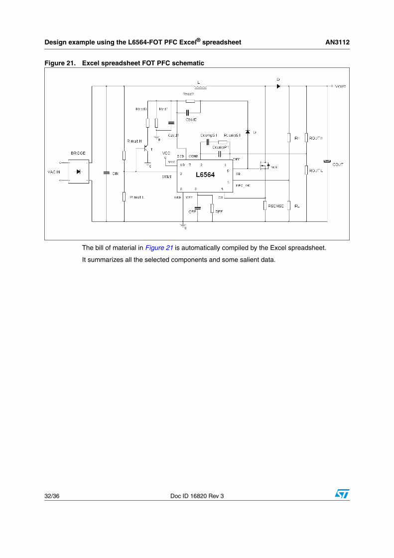
An Excel spreadsheet has been developed to allow a quick and easy design of a boost PFC pre-regulator using the STMicroelectronics L6564 controller, operating in fixed-off-time. Figure 21 shows the first sheet precompiled with the input design data used in Section 4: Designing a fixed-off-time PFC.
Figure 19. Excel spreadsheet design specification input table
Figure 20. Other design data
The tool is able to generate a complete parts list of the PFC schematic represented in Figure 21, including the power dissipation calculation of the main components.
Design example using the L6564-FOT PFC Excel® spreadsheet AN3112
32/36 Doc ID 16820 Rev 3
Figure 21. Excel spreadsheet FOT PFC schematic
The bill of material in Figure 21 is automatically compiled by the Excel spreadsheet.
It summarizes all the selected components and some salient data.

AN3112 Design example using the L6564-FOT PFC Excel® spreadsheet
Doc ID 16820 Rev 3 33/36
Figure 22. Excel spreadsheet BOM
400 W FOT PFC BASED ON L6564 BILL OF MATERIAL
Selected
Value Unit [ ]
BRIDGE RECTIFIER D15XB60
MOSFET P/N 2 x STP12NM50PF
DIODE P/N STTH8R06
Inductor L 500 µH
Max peak Inductor current Ilpkx 9.67 A
Sense resistor Rsx 0.12 Ω Power dissipation Ps 2.14 W
INPUT Capacitor Cin 1 µF
OUTPUT Capacitor Cout 330 µF
Pin3 - MULT Divider Rmult L 51 kΩ
Rmult H 6900 kΩ
ZCD FOT circuit Rzcd1 15 kΩ Rzcd2 1 kΩ Rzcd3 1.5 kΩ Czcd1 220 pF Czcd2 100 pF
Diode P/N 1N4148 pnp-BJT P/N BC857C
Feedback Divider RoutH 3000 kΩ
RoutL 18.8 kΩ
Output divider for PFC_OK RL 51 kΩ
RH 8800 kΩ
Compensation Network CcompP 100 nF CcompS 1000 nF RcompS 56 kΩ
Voltage Feedforward CFF 1000 nF RFF 1000 kΩ
IC Controller L6564
Reference AN3112
34/36 Doc ID 16820 Rev 3
6 Reference
1. A new continuous-time model for current-mode control with constant frequency, constant on-time and constant off-time, in CCM and DCM”, IEEE power electronics specialists conference record, San Antonio, Texas, pp. 382-389, 1990
2. “Current mode control”, venable technical paper #5, www.venableind.com
3. “Fixed-off-time control of PFC pre-regulators”, 10th European conference on power electronics and applications, EPE2003, Toulouse, France, paper 382
4. “L6564, transition-mode PFC controller”, datasheet, www.st.com
5. “Design fixed-off-time-controlled PFC pre-regulators with the L6562”, AN1792
6. “400W FOT-controlled PFC pre-regulator with the L6563”, AN2485
7. “A systematic approach to frequency compensation of the voltage loop in boost PFC pre-regulator”, abstract
AN3112 Revision history
Doc ID 16820 Rev 3 35/36
7 Revision history
Table 1. Document revision history
Date Revision Changes
03-May-2010 1 Initial release.
02-Dec-2010 2 Updated: Section 4.3.7 on page 19.
09-Feb-2011 3 Updated: Figure 11 on page 19.

AN3112
36/36 Doc ID 16820 Rev 3
Please Read Carefully:
Information in this document is provided solely in connection with ST products. STMicroelectronics NV and its subsidiaries (“ST”) reserve theright to make changes, corrections, modifications or improvements, to this document, and the products and services described herein at anytime, without notice.
All ST products are sold pursuant to ST’s terms and conditions of sale.
Purchasers are solely responsible for the choice, selection and use of the ST products and services described herein, and ST assumes noliability whatsoever relating to the choice, selection or use of the ST products and services described herein.
No license, express or implied, by estoppel or otherwise, to any intellectual property rights is granted under this document. If any part of thisdocument refers to any third party products or services it shall not be deemed a license grant by ST for the use of such third party productsor services, or any intellectual property contained therein or considered as a warranty covering the use in any manner whatsoever of suchthird party products or services or any intellectual property contained therein.
UNLESS OTHERWISE SET FORTH IN ST’S TERMS AND CONDITIONS OF SALE ST DISCLAIMS ANY EXPRESS OR IMPLIEDWARRANTY WITH RESPECT TO THE USE AND/OR SALE OF ST PRODUCTS INCLUDING WITHOUT LIMITATION IMPLIEDWARRANTIES OF MERCHANTABILITY, FITNESS FOR A PARTICULAR PURPOSE (AND THEIR EQUIVALENTS UNDER THE LAWSOF ANY JURISDICTION), OR INFRINGEMENT OF ANY PATENT, COPYRIGHT OR OTHER INTELLECTUAL PROPERTY RIGHT.
UNLESS EXPRESSLY APPROVED IN WRITING BY AN AUTHORIZED ST REPRESENTATIVE, ST PRODUCTS ARE NOTRECOMMENDED, AUTHORIZED OR WARRANTED FOR USE IN MILITARY, AIR CRAFT, SPACE, LIFE SAVING, OR LIFE SUSTAININGAPPLICATIONS, NOR IN PRODUCTS OR SYSTEMS WHERE FAILURE OR MALFUNCTION MAY RESULT IN PERSONAL INJURY,DEATH, OR SEVERE PROPERTY OR ENVIRONMENTAL DAMAGE. ST PRODUCTS WHICH ARE NOT SPECIFIED AS "AUTOMOTIVEGRADE" MAY ONLY BE USED IN AUTOMOTIVE APPLICATIONS AT USER’S OWN RISK.
Resale of ST products with provisions different from the statements and/or technical features set forth in this document shall immediately voidany warranty granted by ST for the ST product or service described herein and shall not create or extend in any manner whatsoever, anyliability of ST.
ST and the ST logo are trademarks or registered trademarks of ST in various countries.
Information in this document supersedes and replaces all information previously supplied.
The ST logo is a registered trademark of STMicroelectronics. All other names are the property of their respective owners.
© 2011 STMicroelectronics - All rights reserved
STMicroelectronics group of companies
Australia - Belgium - Brazil - Canada - China - Czech Republic - Finland - France - Germany - Hong Kong - India - Israel - Italy - Japan - Malaysia - Malta - Morocco - Philippines - Singapore - Spain - Sweden - Switzerland - United Kingdom - United States of America
www.st.com