an101 using visible ingan laser diodes from osram opto
TRANSCRIPT
1 / 192018-10-16 | Document No.: AN101
www.osram-os.com
Application Note
Using visible InGaN laser diodes from OSRAM Opto Semiconductors
Abstract
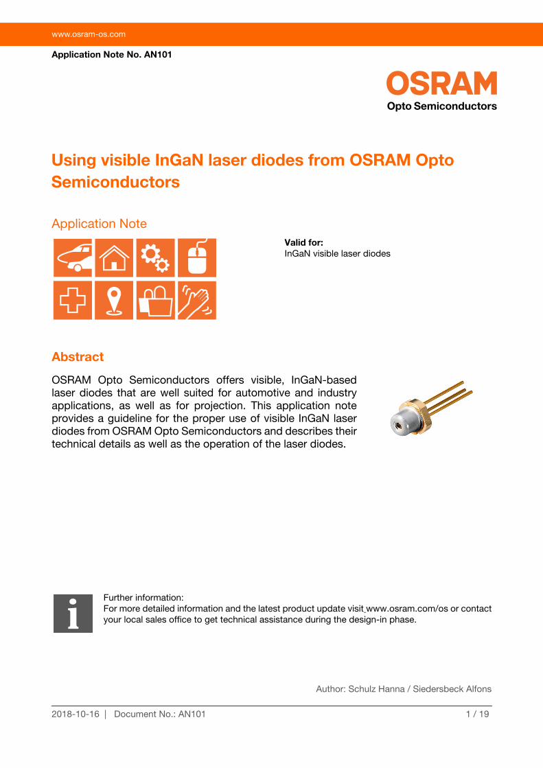
OSRAM Opto Semiconductors offers visible, InGaN-basedlaser diodes that are well suited for automotive and industryapplications, as well as for projection. This application noteprovides a guideline for the proper use of visible InGaN laserdiodes from OSRAM Opto Semiconductors and describes theirtechnical details as well as the operation of the laser diodes.
Valid for:InGaN visible laser diodes
Author: Schulz Hanna / Siedersbeck Alfons
Further information:For more detailed information and the latest product update visit www.osram.com/os or contactyour local sales office to get technical assistance during the design-in phase.
Application Note No. AN101

www.osram-os.com
Table of contents
A. Basic information on handling and assembly .........................................................2
Safety instructions ..............................................................................................2
Storage and shipping ..........................................................................................3
Unpacking and handling .....................................................................................3
Label information ................................................................................................4
ESD handling ......................................................................................................4
Soldering .............................................................................................................6
B. Mounting and thermal management .......................................................................6
Mounting .............................................................................................................6
Thermal management .........................................................................................7
Influence of the mounting on thermal resistance (junction to heat sink) Rth,JH 8
Wavelength shift versus temperature and current ............................................10
Thermal rollover ................................................................................................11
C. Electrical and optical considerations ....................................................................11
Operating conditions ........................................................................................12
Linear regulator .................................................................................................13
Switching regulator ...........................................................................................14
Low power driver solutions ...............................................................................16
High power driver solutions ..............................................................................16
Optical ...............................................................................................................17
D. Appendix ...............................................................................................................18
A. Basic information on handling and assembly
Safety instructions
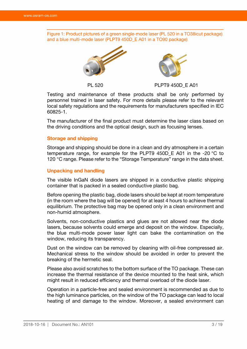
Depending on the mode of operation, laser diodes (refer to Figure 1) emit highlyconcentrated visible light which can be hazardous to the human eye. Productswhich incorporate these devices must follow the safety precautions specified inIEC 60825-1 “Safety of laser products”.
2 / 192018-10-16 | Document No.: AN101
www.osram-os.com
Figure 1: Product pictures of a green single-mode laser (PL 520 in a TO38icut package) and a blue multi-mode laser (PLPT9 450D_E A01 in a TO90 package)
Testing and maintenance of these products shall be only performed bypersonnel trained in laser safety. For more details please refer to the relevantlocal safety regulations and the requirements for manufacturers specified in IEC60825-1.
The manufacturer of the final product must determine the laser class based onthe driving conditions and the optical design, such as focusing lenses.
Storage and shipping
Storage and shipping should be done in a clean and dry atmosphere in a certaintemperature range, for example for the PLPT9 450D_E A01 in the -20 °C to120 °C range. Please refer to the “Storage Temperature” range in the data sheet.
Unpacking and handling
The visible InGaN diode lasers are shipped in a conductive plastic shippingcontainer that is packed in a sealed conductive plastic bag.
Before opening the plastic bag, diode lasers should be kept at room temperature(in the room where the bag will be opened) for at least 4 hours to achieve thermalequilibrium. The protective bag may be opened only in a clean environment andnon-humid atmosphere.
Solvents, non-conductive plastics and glues are not allowed near the diodelasers, because solvents could emerge and deposit on the window. Especially,the blue multi-mode power laser light can bake the contamination on thewindow, reducing its transparency.
Dust on the window can be removed by cleaning with oil-free compressed air.Mechanical stress to the window should be avoided in order to prevent thebreaking of the hermetic seal.
Please also avoid scratches to the bottom surface of the TO package. These canincrease the thermal resistance of the device mounted to the heat sink, whichmight result in reduced efficiency and thermal overload of the diode laser.
Operation in a particle-free and sealed environment is recommended as due tothe high luminance particles, on the window of the TO package can lead to localheating of and damage to the window. Moreover, a sealed environment can
PL 520 PLPT9 450D_E A01
3 / 192018-10-16 | Document No.: AN101
www.osram-os.com
prevent the steel cap of the TO package from aggressive impacts such ascorrosion through interaction with salt.
Mechanical stress on the pins or bending of the pins can lead to damage to thehermetic seal and has a negative effect on long-term stability.
Label information
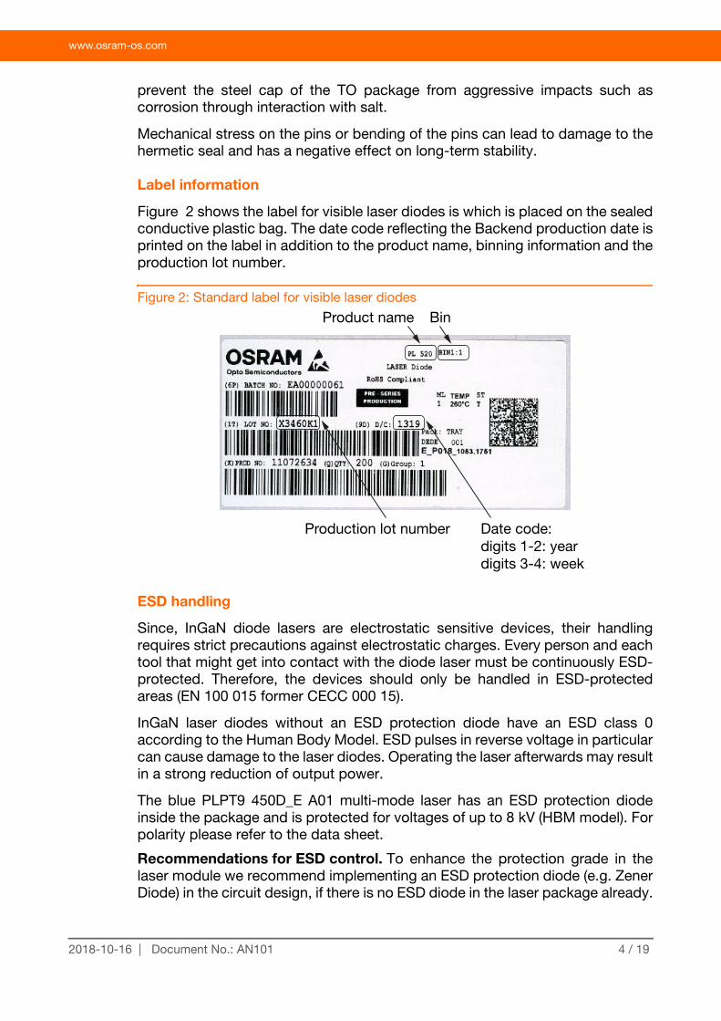
Figure 2 shows the label for visible laser diodes is which is placed on the sealedconductive plastic bag. The date code reflecting the Backend production date isprinted on the label in addition to the product name, binning information and theproduction lot number.
Figure 2: Standard label for visible laser diodes
ESD handling
Since, InGaN diode lasers are electrostatic sensitive devices, their handlingrequires strict precautions against electrostatic charges. Every person and eachtool that might get into contact with the diode laser must be continuously ESD-protected. Therefore, the devices should only be handled in ESD-protectedareas (EN 100 015 former CECC 000 15).
InGaN laser diodes without an ESD protection diode have an ESD class 0according to the Human Body Model. ESD pulses in reverse voltage in particularcan cause damage to the laser diodes. Operating the laser afterwards may resultin a strong reduction of output power.
The blue PLPT9 450D_E A01 multi-mode laser has an ESD protection diodeinside the package and is protected for voltages of up to 8 kV (HBM model). Forpolarity please refer to the data sheet.
Recommendations for ESD control. To enhance the protection grade in thelaser module we recommend implementing an ESD protection diode (e.g. ZenerDiode) in the circuit design, if there is no ESD diode in the laser package already.
Product name Bin
Date code:digits 1-2: yeardigits 3-4: week
Production lot number
4 / 192018-10-16 | Document No.: AN101
www.osram-os.com
The following points must be considered in order to ensure the proper protectionof the diode:
• Breakdown voltage: The breakdown voltage of the ESD protection diodemust be higher than the total forward voltage of the laser diode in order toensure the correct functioning of the circuitry under normal circumstances.
• Response time: The response time of the ESD protection diode must befaster than that of the laser diode. Thereby, the protection mechanism canwork effectively before a pulse may cause any damage to the laser diodes.Due to the fast switching times of the laser diodes, the response time of theprotection diode is supposed to be in the range of 1 ns or less.
Basics for protection against static:
Grounding. Grounding systems shall be used to ensure that devices, personneland any other conductors are at the same electrical potential.
Protection. To avoid exposure to static charges, keep components andmodules separated during storage and transit. Through protection againststatically charged objects and electric fields potential damage to lasercomponents is minimized.
As statically charged insulators cannot be discharged by grounding, it isadvisable to eliminate non-conductive plastic materials and other types ofinsulators from the working place, transit and storage areas.
Neutralization. Neutralization is the process to discharge insulators. Thishappens naturally through the process of ionization. Ions are charged particlesthat are always present in the atmosphere in the form of atoms, molecules orgroups of molecules such as drops of water. The use of an ionizer generatesbillions of ions in the air and enables the static charge on an insulator to leakaway.
Prevention. Prevention can be the most effective and important personalcontribution to eliminate damage caused by ESD. Please find a set of guidelinesbelow:
• Always keep working areas clean and tidy. Remove unwanted objects,especially those made of non-conductive plastic materials.
• When transferring components from one person to another, both personsshould be grounded or at the same voltage potential.
• Avoid laser components or modules coming into contact with anyinsulating material.
• Never enter a static-proof working area without taking the necessaryprecautions.
• Always be aware of these rules when working with devices that can bedamaged by electrostatic discharges.
For further information on ESD handling please refer to the application note “ESDProtection while Handling LEDs“ which also applies to InGaN laser diodes.
5 / 192018-10-16 | Document No.: AN101
www.osram-os.com
Soldering
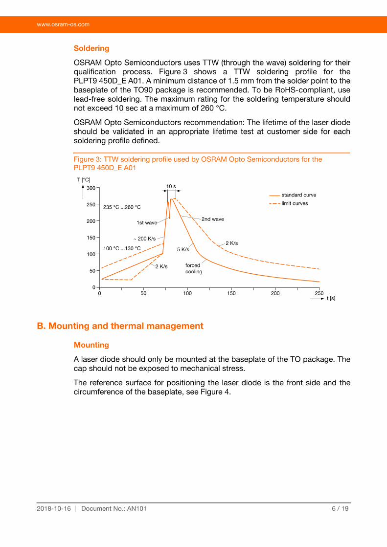
OSRAM Opto Semiconductors uses TTW (through the wave) soldering for theirqualification process. Figure 3 shows a TTW soldering profile for thePLPT9 450D_E A01. A minimum distance of 1.5 mm from the solder point to thebaseplate of the TO90 package is recommended. To be RoHS-compliant, uselead-free soldering. The maximum rating for the soldering temperature shouldnot exceed 10 sec at a maximum of 260 °C.
OSRAM Opto Semiconductors recommendation: The lifetime of the laser diodeshould be validated in an appropriate lifetime test at customer side for eachsoldering profile defined.
Figure 3: TTW soldering profile used by OSRAM Opto Semiconductors for the PLPT9 450D_E A01
B. Mounting and thermal management
Mounting
A laser diode should only be mounted at the baseplate of the TO package. Thecap should not be exposed to mechanical stress.
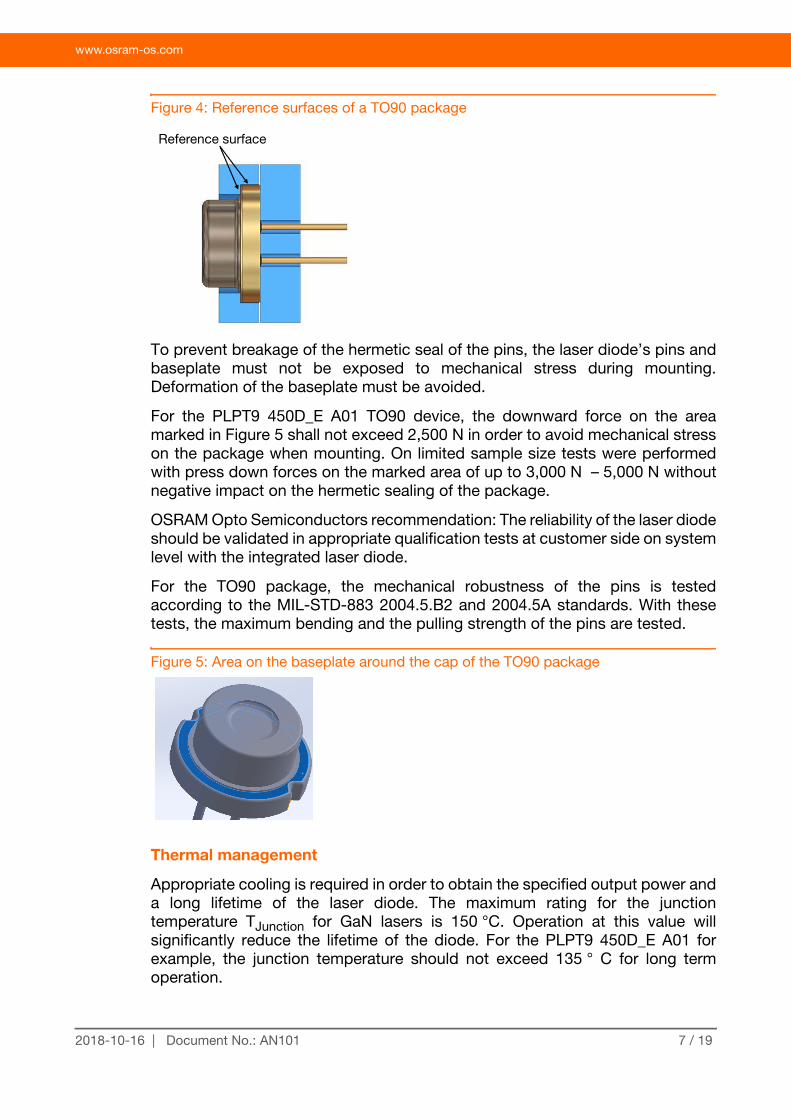
The reference surface for positioning the laser diode is the front side and thecircumference of the baseplate, see Figure 4.
0 50 100 150 200 2500
50
100
150
200
250
300
T [°C]
t [s]
235 °C ...260 °C
100 °C ...130 °C
forcedcooling
standard curve
limit curves
2nd wave1st wave
2 K/s5 K/s
10 s
~ 200 K/s
2 K/s
6 / 192018-10-16 | Document No.: AN101
www.osram-os.com
Figure 4: Reference surfaces of a TO90 package
To prevent breakage of the hermetic seal of the pins, the laser diode’s pins andbaseplate must not be exposed to mechanical stress during mounting.Deformation of the baseplate must be avoided.
For the PLPT9 450D_E A01 TO90 device, the downward force on the areamarked in Figure 5 shall not exceed 2,500 N in order to avoid mechanical stresson the package when mounting. On limited sample size tests were performedwith press down forces on the marked area of up to 3,000 N – 5,000 N withoutnegative impact on the hermetic sealing of the package.
OSRAM Opto Semiconductors recommendation: The reliability of the laser diodeshould be validated in appropriate qualification tests at customer side on systemlevel with the integrated laser diode.
For the TO90 package, the mechanical robustness of the pins is testedaccording to the MIL-STD-883 2004.5.B2 and 2004.5A standards. With thesetests, the maximum bending and the pulling strength of the pins are tested.
Figure 5: Area on the baseplate around the cap of the TO90 package
Thermal management
Appropriate cooling is required in order to obtain the specified output power anda long lifetime of the laser diode. The maximum rating for the junctiontemperature TJunction for GaN lasers is 150 °C. Operation at this value willsignificantly reduce the lifetime of the diode. For the PLPT9 450D_E A01 forexample, the junction temperature should not exceed 135 ° C for long termoperation.
Reference surface
7 / 192018-10-16 | Document No.: AN101
www.osram-os.com
The junction temperature can be calculated using the following equation:
,where Popt is the optical output power, U the operating voltage, I the operatingcurrent, TCase the temperature of the package and Rth the thermal resistance(junction to case).
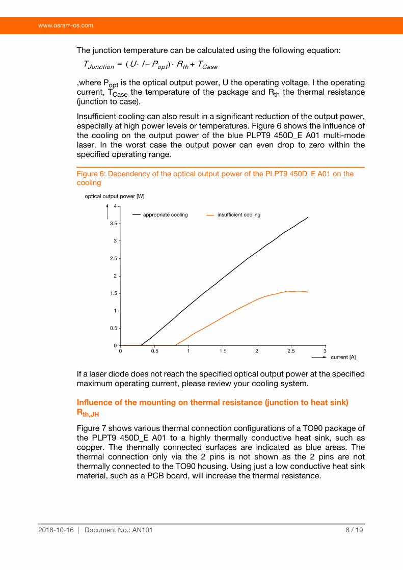
Insufficient cooling can also result in a significant reduction of the output power,especially at high power levels or temperatures. Figure 6 shows the influence ofthe cooling on the output power of the blue PLPT9 450D_E A01 multi-modelaser. In the worst case the output power can even drop to zero within thespecified operating range.
Figure 6: Dependency of the optical output power of the PLPT9 450D_E A01 on the cooling
If a laser diode does not reach the specified optical output power at the specifiedmaximum operating current, please review your cooling system.
Influence of the mounting on thermal resistance (junction to heat sink) Rth,JH
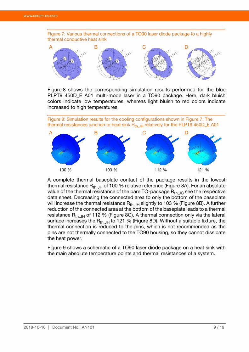
Figure 7 shows various thermal connection configurations of a TO90 package ofthe PLPT9 450D_E A01 to a highly thermally conductive heat sink, such ascopper. The thermally connected surfaces are indicated as blue areas. Thethermal connection only via the 2 pins is not shown as the 2 pins are notthermally connected to the TO90 housing. Using just a low conductive heat sinkmaterial, such as a PCB board, will increase the thermal resistance.
TJunction U I Popt– Rth TCase+=
0
0.5
1
1.5
2
2.5
3
3.5
4
0 0.5 1 1.5 2 2.5 3
appropriate cooling insufficient cooling
current [A]
optical output power [W]
8 / 192018-10-16 | Document No.: AN101
www.osram-os.com
Figure 7: Various thermal connections of a TO90 laser diode package to a highly thermal conductive heat sink
Figure 8 shows the corresponding simulation results performed for the bluePLPT9 450D_E A01 multi-mode laser in a TO90 package. Here, dark bluishcolors indicate low temperatures, whereas light bluish to red colors indicateincreased to high temperatures.
Figure 8: Simulation results for the cooling configurations shown in Figure 7. The thermal resistances junction to heat sink Rth,JH relatively for the PLPT9 450D_E A01
A complete thermal baseplate contact of the package results in the lowestthermal resistance Rth,JH of 100 % relative reference (Figure 8A). For an absolutevalue of the thermal resistance of the bare TO-package Rth,JC see the respectivedata sheet. Decreasing the connected area to only the bottom of the baseplatewill increase the thermal resistance Rth,JH slightly to 103 % (Figure 8B). A furtherreduction of the connected area at the bottom of the baseplate leads to a thermalresistance Rth,JH of 112 % (Figure 8C). A thermal connection only via the lateralsurface increases the Rth,JH to 121 % (Figure 8D). Without a suitable fixture, thethermal connection is reduced to the pins, which is not recommended as thepins are not thermally connected to the TO90 housing, so they cannot dissipatethe heat power.
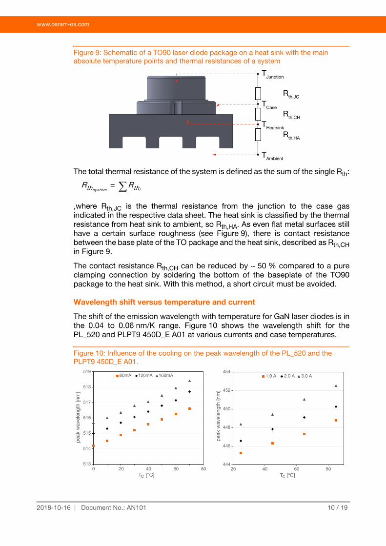
Figure 9 shows a schematic of a TO90 laser diode package on a heat sink withthe main absolute temperature points and thermal resistances of a system.
A B C D
A B C DA B C D
100 % 103 % 112 % 121 %
9 / 192018-10-16 | Document No.: AN101
www.osram-os.com
Figure 9: Schematic of a TO90 laser diode package on a heat sink with the main absolute temperature points and thermal resistances of a system
The total thermal resistance of the system is defined as the sum of the single Rth:
,where Rth,JC is the thermal resistance from the junction to the case gasindicated in the respective data sheet. The heat sink is classified by the thermalresistance from heat sink to ambient, so Rth,HA. As even flat metal surfaces stillhave a certain surface roughness (see Figure 9), there is contact resistancebetween the base plate of the TO package and the heat sink, described as Rth,CHin Figure 9.
The contact resistance Rth,CH can be reduced by ~ 50 % compared to a pureclamping connection by soldering the bottom of the baseplate of the TO90package to the heat sink. With this method, a short circuit must be avoided.
Wavelength shift versus temperature and current
The shift of the emission wavelength with temperature for GaN laser diodes is inthe 0.04 to 0.06 nm/K range. Figure 10 shows the wavelength shift for thePL_520 and PLPT9 450D_E A01 at various currents and case temperatures.
Figure 10: Influence of the cooling on the peak wavelength of the PL_520 and the PLPT9 450D_E A01.
TJunction
TCase
THeatsink
TAmbient
Rth,JC
Rth,CH
Rth,HA
RthsystemRthi=
513
514
515
516
517
518
519
0 20 40 60 80Tc [°C]
80mA 120mA 160mA
444
446
448
450
452
454
20 40 60 80
pea
k w
avel
engt
h [n
m]
Tc [°C]
1.0 A 2.0 A 3.0 A
pea
k w
avel
engt
h [n
m]
10 / 192018-10-16 | Document No.: AN101
www.osram-os.com
Thermal rollover
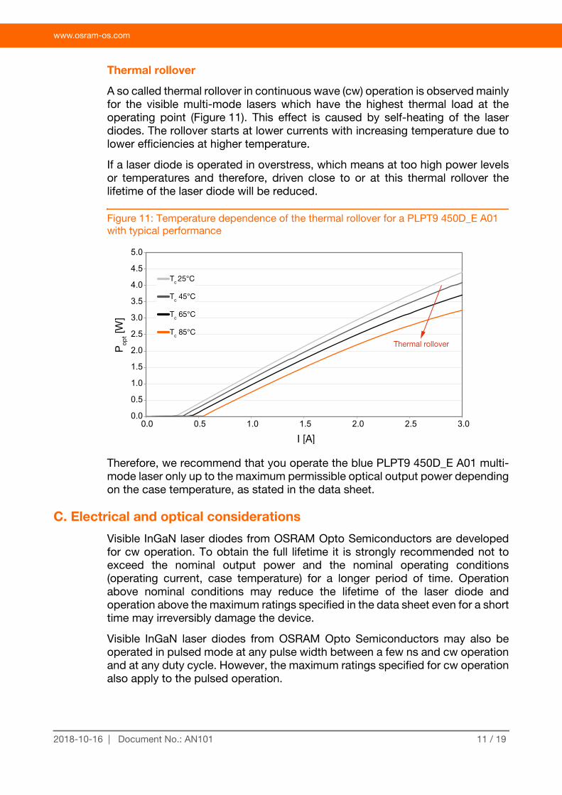
A so called thermal rollover in continuous wave (cw) operation is observed mainlyfor the visible multi-mode lasers which have the highest thermal load at theoperating point (Figure 11). This effect is caused by self-heating of the laserdiodes. The rollover starts at lower currents with increasing temperature due tolower efficiencies at higher temperature.
If a laser diode is operated in overstress, which means at too high power levelsor temperatures and therefore, driven close to or at this thermal rollover thelifetime of the laser diode will be reduced.
Figure 11: Temperature dependence of the thermal rollover for a PLPT9 450D_E A01 with typical performance
Therefore, we recommend that you operate the blue PLPT9 450D_E A01 multi-mode laser only up to the maximum permissible optical output power dependingon the case temperature, as stated in the data sheet.
C. Electrical and optical considerations
Visible InGaN laser diodes from OSRAM Opto Semiconductors are developedfor cw operation. To obtain the full lifetime it is strongly recommended not toexceed the nominal output power and the nominal operating conditions(operating current, case temperature) for a longer period of time. Operationabove nominal conditions may reduce the lifetime of the laser diode andoperation above the maximum ratings specified in the data sheet even for a shorttime may irreversibly damage the device.
Visible InGaN laser diodes from OSRAM Opto Semiconductors may also beoperated in pulsed mode at any pulse width between a few ns and cw operationand at any duty cycle. However, the maximum ratings specified for cw operationalso apply to the pulsed operation.
0.0
0.5
1.0
1.5
2.0
2.5
3.0
3.5
4.0
4.5
5.0
0.0 0.5 1.0 1.5 2.0 2.5 3.0
Po
pt [
W]
I [A]
Tc 25°C
Tc 45°C
Tc 65°C
Tc 85°C
Thermal rollover
11 / 192018-10-16 | Document No.: AN101
www.osram-os.com
Furthermore, please note that the output power of the laser diode depends onthe temperature. Thus, for applications that require constant output power overa broad range of temperatures, an automated power control (APC) is required. Aphotodiode (PD) is usually adopted to optically monitor the output power of thelaser diode. OSRAM Opto Semiconductors provides a series of photo detectorswith compact size and high sensitivity which are suitable for APC (refer to theAppendix, Table 1).
Operating conditions
As a semiconductor laser is inherently a current-driven device, a true currentsource is recommended for driving laser diodes.
Laser diodes must not be driven by a voltage source. Similar to LEDs, theforward voltage depends on the junction temperature and differs from device todevice.
An ideal power supply for a laser diode has the following characteristics:
• Current source
• Transient suppression (also low noise)
• Independent clamping current limit
• Slow start / ramping the current signal during switch-on
• Output overvoltage protection
• Input undervoltage detection
• Output short-circuit / interruption detection
• Shorting output during driver off status for ESD protection
• No undershooting of the output voltage at switch-off of the laser, so that anegative voltage over the laser diode cannot occur.
As a laser diode has a very short rise time and the mirrors of the resonator arethe most sensitive parts of the design, even short current peaks beyond themaximum data sheet conditions may lead to a catastrophic optical mirrordamage (COMD) resulting in a significant reduction of optical output power.Especially when switching the laser diode on and off, transient currents beyondthe maximum conditions can occur which must be blocked.
For this reason, the maximum conditions for current and optical output powergiven in the data sheet must not be exceeded, not even in pulse mode.
Mains supply circuits should be designed to block external noise sources suchas inductive loads. Battery-driven designs are more relaxed in this regard.External in-coupling of noise can be reduced by a circuit design with shortconnection paths between the laser driver and laser diode.
Laser diodes shall be driven with a regulated driver, so either in constant currentmode (ACC Automatic Current Control) or constant optical power mode (APC
12 / 192018-10-16 | Document No.: AN101
www.osram-os.com
Automatic Power Control). For APC control a photo diode is used to feed backthe optical output power detected in order to control the laser diode current tomaintain constant optical output power.
To protect against turn-on transients, a laser diode driver should feature a slow-start circuit at switch on. The slope of the turn on ramp should be appliedaccording to the application needs.
Moreover, there is a need to limit the output current. Otherwise damage to themirror facet may result.
A separate overvoltage protection of the power supply ensures that the outputvoltage is limited in terms of changes of impedance of the load, e.g. interruptionof the load connection.
An input undervoltage detection ensures the proper control of the constantcurrent regulator to start working after the full input voltage is applied.
Ideal laser diode drivers offer a shorting feature to maintain the output leads atthe same electrical potential when the laser is not being operated. This shortingoutput feature offers ideal ESD protection during off status.
When switching off the laser diode an undershooting of the output voltage is notallowed as the laser diode is not designed for application of reverse voltages.
Most integrated driver solutions provide the above-mentioned safety featuresand only require a few additional external parts.
Especially for a cold start, the temperature dependency of the forward voltage ofthe laser diode has an influence on the switch-on behavior of the laser diodedriver.
For example, with proper thermal connection of the PLPT9 450D_E A01 themajor part of the heat-up of the laser diode — not of the system — takes placewithin ~100 ms, which means that most of the thermally caused changes of theforward voltage at one operating point are within this period of time.
OSRAM Opto Semiconductors recommendation: The lifetime of the laser diodeshould be validated in an appropriate lifetime test at customer side for the driverdesign used.
OSRAM Opto Semiconductors cannot be held liable for the completeness of therecommendations. The customer must perform his own tests to verify thedesign.
There are 2 main driver topologies for constant current drivers:
• Linear regulator
• Switching regulator
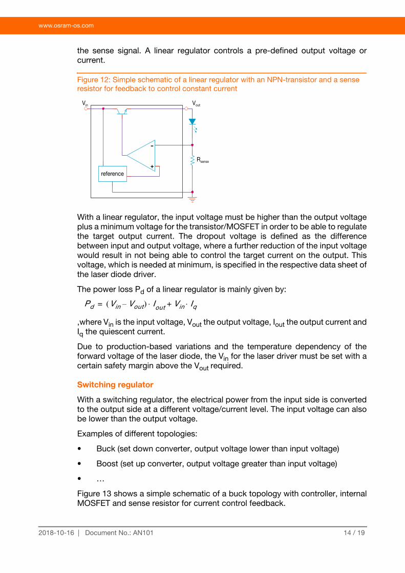
Linear regulator
Described simply, a linear regulator consists of 3 parts as shown in Figure 12: areference voltage, a transistor/MOSFET and an amplifier for feedback control of
13 / 192018-10-16 | Document No.: AN101
www.osram-os.com
the sense signal. A linear regulator controls a pre-defined output voltage orcurrent.
Figure 12: Simple schematic of a linear regulator with an NPN-transistor and a sense resistor for feedback to control constant current
With a linear regulator, the input voltage must be higher than the output voltageplus a minimum voltage for the transistor/MOSFET in order to be able to regulatethe target output current. The dropout voltage is defined as the differencebetween input and output voltage, where a further reduction of the input voltagewould result in not being able to control the target current on the output. Thisvoltage, which is needed at minimum, is specified in the respective data sheet ofthe laser diode driver.
The power loss Pd of a linear regulator is mainly given by:
,where Vin is the input voltage, Vout the output voltage, Iout the output current andIq the quiescent current.
Due to production-based variations and the temperature dependency of theforward voltage of the laser diode, the Vin for the laser driver must be set with acertain safety margin above the Vout required.
Switching regulator
With a switching regulator, the electrical power from the input side is convertedto the output side at a different voltage/current level. The input voltage can alsobe lower than the output voltage.
Examples of different topologies:
• Buck (set down converter, output voltage lower than input voltage)
• Boost (set up converter, output voltage greater than input voltage)
• …
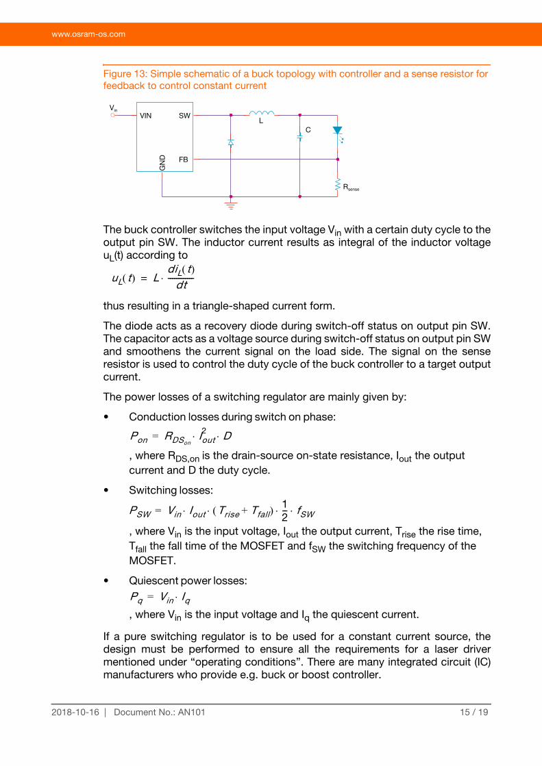
Figure 13 shows a simple schematic of a buck topology with controller, internalMOSFET and sense resistor for current control feedback.
-
+reference
Rsense
VoutVin
Pd Vin Vout– I out Vin Iq+=
14 / 192018-10-16 | Document No.: AN101
www.osram-os.com
Figure 13: Simple schematic of a buck topology with controller and a sense resistor for feedback to control constant current
The buck controller switches the input voltage Vin with a certain duty cycle to theoutput pin SW. The inductor current results as integral of the inductor voltageuL(t) according to
thus resulting in a triangle-shaped current form.
The diode acts as a recovery diode during switch-off status on output pin SW.The capacitor acts as a voltage source during switch-off status on output pin SWand smoothens the current signal on the load side. The signal on the senseresistor is used to control the duty cycle of the buck controller to a target outputcurrent.
The power losses of a switching regulator are mainly given by:
• Conduction losses during switch on phase:
, where RDS,on is the drain-source on-state resistance, Iout the output current and D the duty cycle.
• Switching losses:
, where Vin is the input voltage, Iout the output current, Trise the rise time, Tfall the fall time of the MOSFET and fSW the switching frequency of the MOSFET.
• Quiescent power losses:
, where Vin is the input voltage and Iq the quiescent current.
If a pure switching regulator is to be used for a constant current source, thedesign must be performed to ensure all the requirements for a laser drivermentioned under “operating conditions”. There are many integrated circuit (IC)manufacturers who provide e.g. buck or boost controller.
Rsense
Vin
VIN SW
FBG
ND
CL
uL t LdiL t
dt------------=
Pon RDSonIout2 D =
PSW Vin Iout Trise Tfall+ 12-- fSW =
Pq Vin Iq=
15 / 192018-10-16 | Document No.: AN101
www.osram-os.com
Low power driver solutions
For low power applications, the most common driver topology is the linearregulator, as the absolute power losses are relatively low and the requirementsfor a laser diode driver as mentioned in the “Operating conditions” chapter areeasier to fulfill compared to a pure switching regulator.
For example, the laser diode driver iC-NZN (www.ichaus.de/ic-nzn) from themanufacturer iC-Haus GmbH allows CW operation and switching with definedcurrent pulses up to 155 MHz in controlled burst mode with currents up to300 mA. “Controlled” means that a pre-set operating point is maintained duringthe burst phase via the LVDS/TTL switching input. The driver enables both APCand ACC mode with the setting of an external resistor. It features a laser currentlimitation, a fast soft-start function and strong transient suppression with smallexternal capacitors.
High power driver solutions
Especially with high current loads, the drop-out voltage of a linear regulator mustbe kept as low as possible to minimize power dissipation.
For the PLPT9 450D_E A01, high power laser diode the CW power laser diodedriver iC-HTG (www.ichaus.de/htg) from the manufacturer iC-Haus GmbH offersprecise constant current control with minimal external component count. Anexternal power transistor and a shunt resistor (Rsense) are used to set up aclosed-loop current driver either in ACC or APC mode. The external powertransistor (P-channel or N-channel) can be driven by connecting the gate of thetransistor to the pin VRP or VPN, respectively. All the parameters, including theinternal reference voltages, can be set via serial communication (I²C or SPI).
In APC mode, an internal programmable logarithmic monitor resistor (PLR) or anexternal monitor resistor can be selected to close the control loop.
In ACC mode, the laser diode current can be measured by the use of a lowimpedance shunt resistor to minimize the power losses.
The output power can be analog modulated with a frequency of up to 50 kHz.
The iC-HTG allows the laser channel to be disabled when an overcurrentthreshold has been exceeded. This overcurrent threshold is programmable usingan 8-bit linear D/A converter.
For efficiency enhancement, the iC-HTG offers the feature via a DCO output pinto control the output voltage of an external DC/DC converter as supply voltageof the laser diode in order to allow the linear regulator to work at the lowestpossible supply voltage close to the dropout voltage. This reduces power losseswhile maintaining the preset current for the laser.
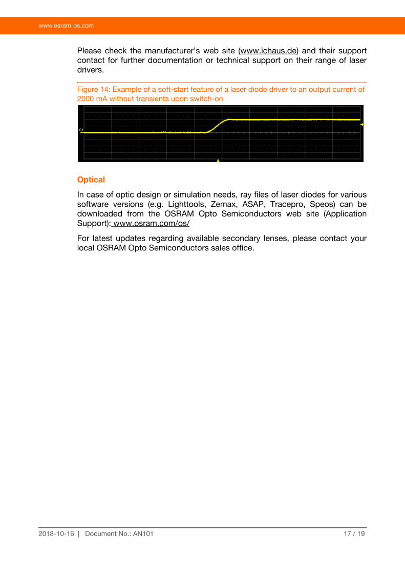
Figure 14 shows an example of the soft-start current feature after switch-on ofthe iC-HTG laser diode driver for the PLPT9 450D_E A01 to ramp up to 2000 mAwithout any transients beyond maximum conditions.
16 / 192018-10-16 | Document No.: AN101
www.osram-os.com
Please check the manufacturer’s web site (www.ichaus.de) and their supportcontact for further documentation or technical support on their range of laserdrivers.
Figure 14: Example of a soft-start feature of a laser diode driver to an output current of 2000 mA without transients upon switch-on
Optical
In case of optic design or simulation needs, ray files of laser diodes for varioussoftware versions (e.g. Lighttools, Zemax, ASAP, Tracepro, Speos) can bedownloaded from the OSRAM Opto Semiconductors web site (ApplicationSupport): www.osram.com/os/
For latest updates regarding available secondary lenses, please contact yourlocal OSRAM Opto Semiconductors sales office.
17 / 192018-10-16 | Document No.: AN101
www.osram-os.com
D. Appendix
Selected photo detectors available for APC (www.osram.com/os/)
Table 1: Series of compact-size and high sensitivity photo detectors from OSRAM Opto Semiconductors, which are suitable for APC feature
Part number Picture Spectrum range Package size
SFH 2701 400~1050 nm 1.5 * 3.2 * 1.1 mm³
SFH 2430 400~900 nm 4.4 * 3.85 * 1.15 mm³
SFH 3711 440~690 nm 2 * 1.28 * 0.8 mm³
SFH 3204 420~1100 nm 1.1 * 3.0 * 1.2 mm³
SFH 2201 300~1100 nmenhanced blue/green sensitivity
4.0 * 5.1 * 0.85 mm³
18 / 192018-10-16 | Document No.: AN101
www.osram-os.com
Don't forget: LED Light for you is your place tobe whenever you are looking for information orworldwide partners for your LED Lightingproject.
www.ledlightforyou.com
ABOUT OSRAM OPTO SEMICONDUCTORS
OSRAM, Munich, Germany is one of the two leading light manufacturers in the world. Its subsidiary, OSRAMOpto Semiconductors GmbH in Regensburg (Germany), offers its customers solutions based on semiconduc-tor technology for lighting, sensor and visualization applications. OSRAM Opto Semiconductors has produc-tion sites in Regensburg (Germany), Penang (Malaysia) and Wuxi (China). Its headquarters for North Americais in Sunnyvale (USA), and for Asia in Hong Kong. OSRAM Opto Semiconductors also has sales offices th-roughout the world. For more information go to www.osram-os.com.
DISCLAIMER
PLEASE CAREFULLY READ THE BELOW TERMS AND CONDITIONS BEFORE USING THE INFORMA-TION SHOWN HEREIN. IF YOU DO NOT AGREE WITH ANY OF THESE TERMS AND CONDITIONS, DONOT USE THE INFORMATION.
The information provided in this general information document was formulated using the utmost care; howe-ver, it is provided by OSRAM Opto Semiconductors GmbH on an “as is” basis. Thus, OSRAM Opto Semicon-ductors GmbH does not expressly or implicitly assume any warranty or liability whatsoever in relation to thisinformation, including – but not limited to – warranties for correctness, completeness, marketability, fitnessfor any specific purpose, title, or non-infringement of rights. In no event shall OSRAM Opto SemiconductorsGmbH be liable – regardless of the legal theory – for any direct, indirect, special, incidental, exemplary, con-sequential, or punitive damages arising from the use of this information. This limitation shall apply even ifOSRAM Opto Semiconductors GmbH has been advised of possible damages. As some jurisdictions do notallow the exclusion of certain warranties or limitations of liabilities, the above limitations and exclusions mightnot apply. In such cases, the liability of OSRAM Opto Semiconductors GmbH is limited to the greatest extentpermitted in law.
OSRAM Opto Semiconductors GmbH may change the provided information at any time without giving noticeto users and is not obliged to provide any maintenance or support related to the provided information. Theprovided information is based on special conditions, which means that the possibility of changes cannot beprecluded.
Any rights not expressly granted herein are reserved. Other than the right to use the information provided inthis document, no other rights are granted nor shall any obligations requiring the granting of further rights beinferred. Any and all rights and licenses regarding patents and patent applications are expressly excluded.
It is prohibited to reproduce, transfer, distribute, or store all or part of the content of this document in any formwithout the prior written permission of OSRAM Opto Semiconductors GmbH unless required to do so in ac-cordance with applicable law.
OSRAM Opto Semiconductors GmbH
Head office:
Leibnizstr. 493055 RegensburgGermanywww.osram-os.com
19 / 192018-10-16 | Document No.: AN101