an068 - design steps and results for changing pcb layer
TRANSCRIPT

Application Note AN068 Adapting TI LPRF Reference Designs for Layer Stacking
By Rea Schmid Keywords • Board Stacking for RF Design • VSWR changes with Stacking • Bandwidth and Layer Stacking • PCB for CC25xx Devices • 062 Mil Layer Stacking • FR4 Dielectric Material • EM for Low Power Wireless • Board performance for RF Design
• Matching networks for RF Boards • Discrete Component Balun Design • Smith Charts and Balun • PCB Traces on Smith Charts • Matching to antenna • RF Filter Design • CC24xx, CC25xx •
1 Introduction
Texas Instruments provides Evaluation Modules (EMs) for easy characterization of the Low Power RF (LPRF) products. Using an EM board provides a means to understand the radio’s operation and decreases the product development time. Often a customer will copy the EM layout and then make small changes that can cause the RF performance to change. One of the more common board changes is to modify the board’s layer stacking. For an RF layout this can change the trace impedances in the matching network path and lead to degraded system performance. To deal with PCB stacking layer changes one must maintain the trace impedances when copying an original design. Unlike low frequency designs where one simply adjusts a resistor value for a desired voltage level, the RF traces, along with the discrete components, form a complex impedance matching network. Making sure the impedance is the same after making changes is important to ensure the solution works similar to the original. All TI radios specify recommended load impedance that is found in the data sheet’s parameter section. This number is used to design the balun and matching network to connect to the antenna. This application note discusses taking a reference design and scaling the RF traces when a new stacking height is desired. There are many PCB board factors that affect RF parameters when designing these types of networks. The effects of board material, component package, trace
impedance, and vias are discussed in this application note when changing layer stacking. Measuring or validating board changes is especially challenging at high frequencies. Special equipment such as a VNA or TDR is necessary for extracting S-parameters to assure the final results are correct. In this application note the Smith Chart is used as a tool to derive or validate component values and trace lengths. Finally the results are compared using 3-D magnetic simulation program. A 2-layer Evaluation Module (EM) CC2500 radio was used to show the steps when changing a board’s height from 31 mil (0.8 mm) to 62 mil (1.6 mm). The 62 mil board has the same general RF layout, balun and filter as the original board. Note that different radios (e.g., CC2520, CC2530, etc.) do have different output impedances; therefore each requires a unique matching network. However, the design steps will remain the same. Multi-layer boards, however, can require additional steps. Finally the tools mentioned in this application note are readily available for scaling trace lines and plot their impedances. The tools used in this application note were from Agilent’s ADS software package. Many companies have line calculators and Smith Plotting Tools, so feel free to choose what fits your budget.
SWRA236A Page 1 of 18
Table of Contents KEYWORDS..............................................................................................................................1 1 INTRODUCTION .............................................................................................................1 2 ABBREVIATIONS...........................................................................................................2 3 EM PURPOSE.................................................................................................................3 4 CHANGING BOARD STACKING...................................................................................3
4.1 INCREASING STACKING HEIGHT ON THE EM PCB.........................................................3 4.2 2-SIDED BOARD LAYOUT ............................................................................................4 4.3 PARAMETERS THAT AFFECT PCB TRACES...................................................................5
5 BALUN AND MATCHING FILTER ANALYSIS..............................................................6 5.1 DIFFERENTIAL OUTPUT AND BALUN/MATCHING NETWORK............................................6 5.2 DIFFERENTIAL TO SINGLE-ENDED SOURCE ..................................................................6 5.3 BALUN VALUES ..........................................................................................................7 5.4 LAYOUT TRACE IMPEDANCES ......................................................................................8
6 CHECKING BALUN VALUES WITH SMITH CHART....................................................9 7 PI MATCHING FILTER AND 50 OHM LINE.................................................................11 8 SOFTWARE SIMULATION RESULTS.........................................................................13 9 POWER SUPPLY DECOUPLING.................................................................................14 10 LAB MEASUREMENTS................................................................................................15
10.1 BALUN / MATCHING NETWORK MEASUREMENTS.........................................................15 10.2 RADIO SENSITIVITY COMPARISON..............................................................................16 10.3 TRANSMIT POWER OUTPUT COMPARISON .................................................................17 10.4 SPECTRUM OF IN AND OUT BAND NOISE....................................................................17 10.5 SUMMARY ................................................................................................................18
11 REFERENCES ..............................................................................................................18 12 GENERAL INFORMATION TOOLS AND SOFTWARE ..............................................18
12.1 DOCUMENT HISTORY................................................................................................18
2 Abbreviations
Balun Balanced to unbalanced transformer EM Evaluation Module FR4 PCB board substrate standard LPRF Low Power RF mil 1 thousandth of an inch mm millimeters PCB Printed Circuit Board RX Receive Mode SMA Coaxial PCB connector TDR Time Domain Reflectometer (test equipment) TEM Transverse Electric Magnetic Mode TX Transmit Mode VNA Vector Network Analyzer (test equipment) XOSC Crystal oscillator
SWRA236A Page 2 of 18

3 EM Purpose
A TI LPRF evaluation module (EM) provides a simple evaluation unit to quickly learn the technical operation of a low power wireless radio. The board demonstrates both transmit/receive modes, therefore making it easy to gather link budget information about the device and its antenna. The TI EM is a tested unit and helps to show the engineer a recommended RF layout. Using an EM is good practice and an excellent reference to compare or copy as your final design. TI’s EMs along with development tools like SmartRF® Studio provides a complete platform for design and measurements. TI EM’s provide the following:
1. RX performance measurements (e.g. sensitivity, selectivity, blocking, saturation, spurious emission)
2. TX performance measurements (e.g. output power, occupied bandwidth, adjacent channel power, phase noise, spurious emission)
3. Differential to single-ended conversion 4. Matching to antenna’s whip, monopoles or chip 5. Proper routing of ground and power returns 6. Low electro magnetic emissions 7. Working Antenna
Radio designs require certification depending up on the geographic area. TI EM boards have acceptable levels for radio standards, so if one changes the design they can alter the performance. All CC2500 EM’s Gerber files are available on TI web site at:
http://focus.ti.com/docs/toolsw/folders/print/cc2500_refdes_062.html. http://focus.ti.com/docs/toolsw/folders/print/cc2500em_refdes.html
All calculations were done in mils, but can easily be converted to meters by the following expression
minchmil µ4.25)(1000
11 ==
4 Changing Board Stacking
RF designs are highly dependent upon the signal path from the radio to the antenna. This signal path usually consists of a balun/filter and 50 ohm transmission line. Signal paths can be a combination of discrete and traces or just microstrip traces or some other type of transmission line. This application note starts with a CC2500 EM with 31 mil (0.8 mm) layer spacing and demonstrates how to change the board’s stacking to 62 mil (1.6 mm), while keeping the same RF performance as provided on the original.
4.1 Increasing Stacking Height on the EM PCB
Before changing or copying a reference designs one should document certain parameters so that after changes are made you can check against the original design. One parameter is VSWR, which is a measurement of how much power is delivered to the reflected. A VSWR of 2 would mean 90% of the power is delivered and the insertion loss is 1 dB. When modifying a reference design here is a list of the steps to follow when changing the board’s stacking height:
• Measure traces: lengths, widths and stacking layers using a Gerber Viewer. • Enter values in a Line Calculator to determine the impedances at the original stacking height. • Adjust to new stacking height and adjust traces to equivalent impedance as the original. • Re-adjust decoupling capacitors for in or out of band spurs or noise as needed.
SWRA236A Page 3 of 18
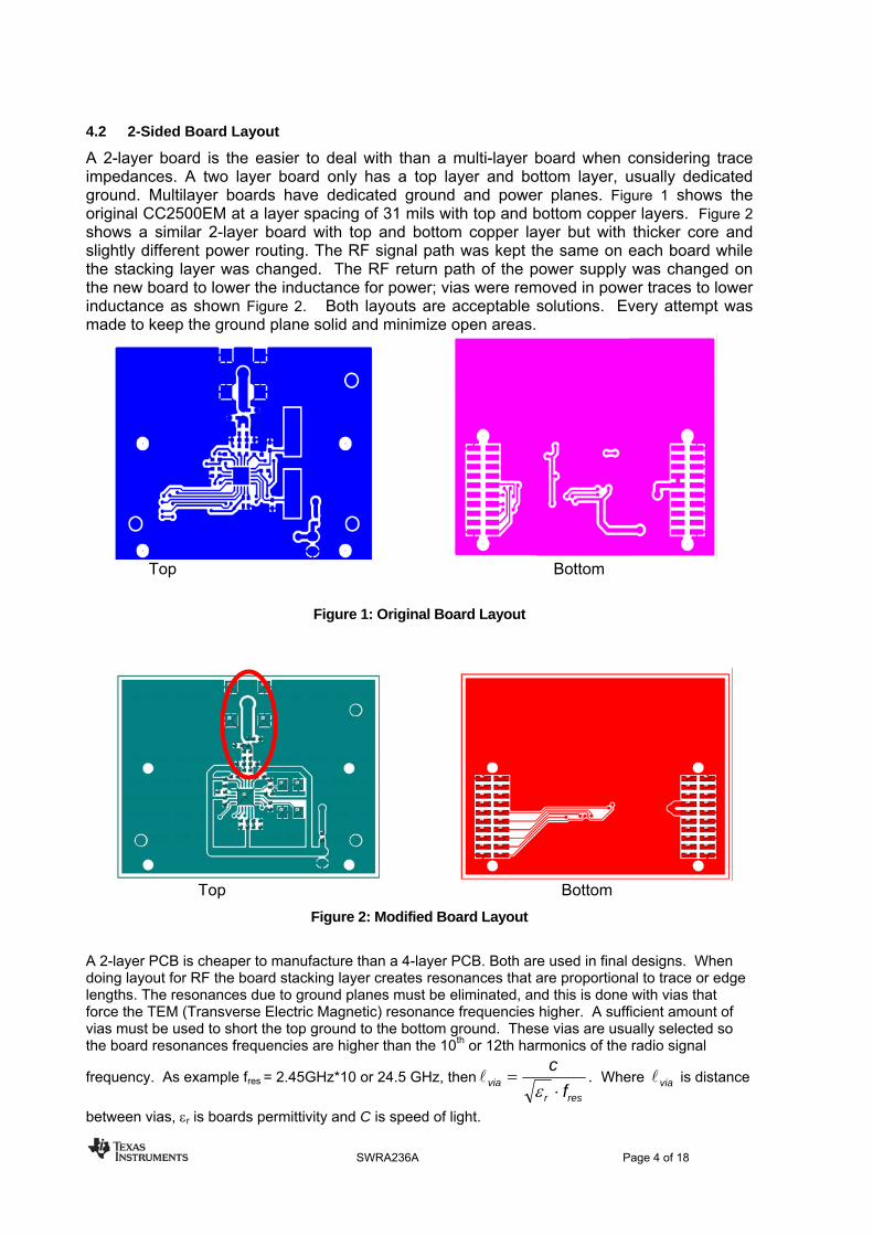
4.2 2-Sided Board Layout
A 2-layer board is the easier to deal with than a multi-layer board when considering trace impedances. A two layer board only has a top layer and bottom layer, usually dedicated ground. Multilayer boards have dedicated ground and power planes. Figure 1 shows the original CC2500EM at a layer spacing of 31 mils with top and bottom copper layers. Figure 2 shows a similar 2-layer board with top and bottom copper layer but with thicker core and slightly different power routing. The RF signal path was kept the same on each board while the stacking layer was changed. The RF return path of the power supply was changed on the new board to lower the inductance for power; vias were removed in power traces to lower inductance as shown Figure 2. Both layouts are acceptable solutions. Every attempt was made to keep the ground plane solid and minimize open areas.
Top Bottom
Figure 1: Original Board Layout
Top Bottom
Figure 2: Modified Board Layout
A 2-layer PCB is cheaper to manufacture than a 4-layer PCB. Both are used in final designs. When doing layout for RF the board stacking layer creates resonances that are proportional to trace or edge lengths. The resonances due to ground planes must be eliminated, and this is done with vias that force the TEM (Transverse Electric Magnetic) resonance frequencies higher. A sufficient amount of vias must be used to short the top ground to the bottom ground. These vias are usually selected so the board resonances frequencies are higher than the 10th or 12th harmonics of the radio signal
frequency. As example fres = 2.45GHz*10 or 24.5 GHz, thenresr
via fc⋅
=ε
l . Where is distance
between vias, ε
vial
r is boards permittivity and C is speed of light.
SWRA236A Page 4 of 18

4.3 Parameters that Affect PCB Traces The stacking height alters the microstrip trace impedance. Using short traces in the balun and filter design allows one to include them in the matching network. For RF, the board parameter that affects trace impedance is the dielectric constant (relative permittivity). Every board manufacturer specifies a permittivity number at a particular frequency. Since the materials different, number varies from manufacturer to manufacturer. Adjusting RF trace impedances for a given PCB board’s dielectric constant is done by calculating its impedance from an effective permittivity, εeff, value that is based upon the width and height of the trace above ground. This number is always less than the boards (εr) permittivity provided by the manufacturer. Assuming that the thickness of the trace, t, is small compared to the height (t/h < 0.005), the εeff value adjusts the impedance of the line when more than one dielectric media is involved as shown below:
The stacking height alters the microstrip trace impedance. Using short traces in the balun and filter design allows one to include them in the matching network. For RF, the board parameter that affects trace impedance is the dielectric constant (relative permittivity). Every board manufacturer specifies a permittivity number at a particular frequency. Since the materials different, number varies from manufacturer to manufacturer. Adjusting RF trace impedances for a given PCB board’s dielectric constant is done by calculating its impedance from an effective permittivity, ε
eff, value that is based upon the width and height of the trace above ground. This number is always less than the boards (εr) permittivity provided by the manufacturer. Assuming that the thickness of the trace, t, is small compared to the height (t/h < 0.005), the εeff value adjusts the impedance of the line when more than one dielectric media is involved as shown below:
1<wh
)4
8ln(60h
ww
hZeff
o ⋅+
⋅⋅=
ε
⎥⎥⎥⎥
⎦
⎤
⎢⎢⎢⎢
⎣
⎡
⎟⎟⎠
⎞⎜⎜⎝
⎛⎟⎠⎞
⎜⎝⎛−+
⋅+⋅
−+
+=
2
104.0121
12
12
1hw
wh
e rreff
εε
Where
h is the board stacking layer spacing w is the trace width
εeff is the scaling dielectric constant for trace width to height ratios A good line calculator takes into account the effects of two media air and board material when calculating the trace impedance for PCB boards. Note that as the impedance changes by the square root of permittivity of the new material; its sensitivity is relatively low over a typical range, as shown in the plot of Figure 3. A greater impedance change occurs due to the stacking height as shown in Figure 3. The value of permittivity used for this plot was 3.9 at 2.45 GHz. At lower frequencies such as 915 MHz the permittivity will increase to approximately 4.2 to 4.7; for higher frequencies (2.45GHz) the lower the permittivity range for most FR4 material typically around 3.8 to 4.2
Impedance change with stacking height
3035404550556065707580
2 2.05 2.1 2.15 2.2
Permitivity Square Root er
Impe
danc
e Zo
59 mil
30 mil
Figure 3: Impedance Plot versus Permittivity for Two Layer Stacking Heights
An easy rule of thumb for checking traces is the line impedance for 50 ohms has a ratio of 2:1 of width to height. As lines become wider the impedance goes down and vice-versa. This can help you when
SWRA236A Page 5 of 18
determining the board spacing requirements or in the design of multi-layer boards to control widths and impedances.
5 Balun and Matching Filter Analysis
An easy way to check a matching network is to plot the network on a Smith Chart. The Smith Chart provides a visual indication of how well the circuit matches the two impedances. In this section the circuit is simplified from the differential for easier understanding when plotting on the Smith Chart.
5.1 Differential Output and Balun/Matching Network
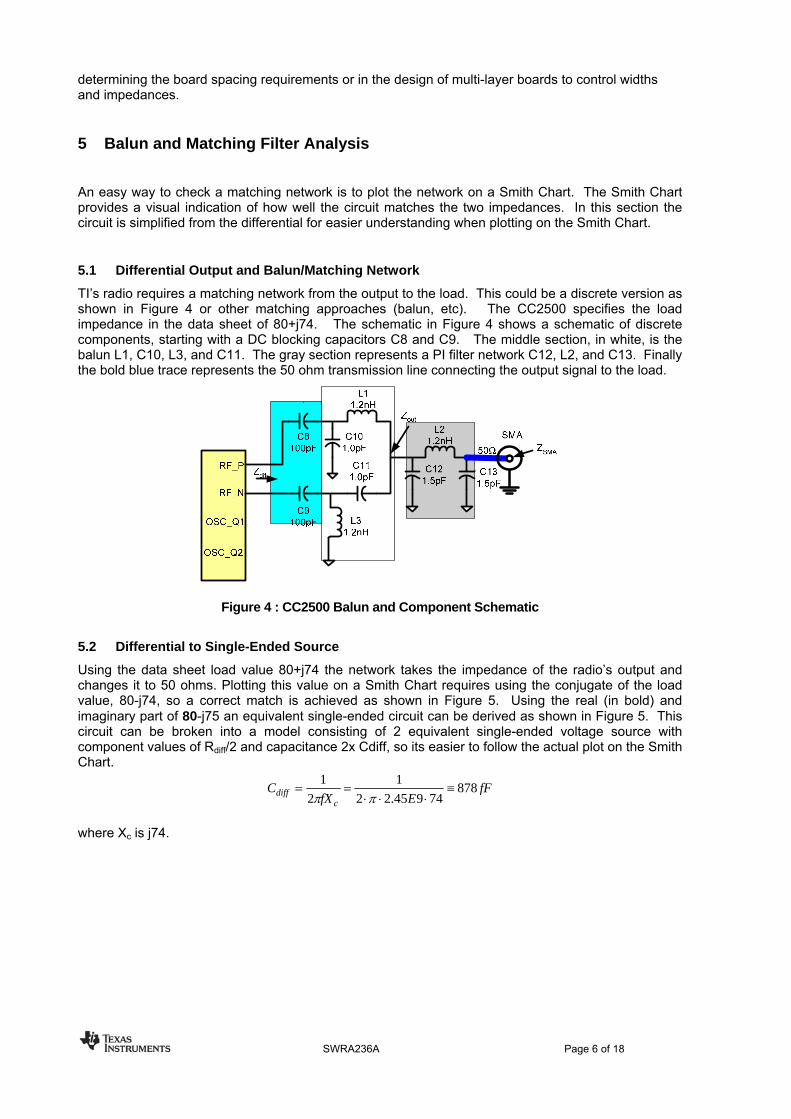
TI’s radio requires a matching network from the output to the load. This could be a discrete version as shown in Figure 4 or other matching approaches (balun, etc). The CC2500 specifies the load impedance in the data sheet of 80+j74. The schematic in Figure 4 shows a schematic of discrete components, starting with a DC blocking capacitors C8 and C9. The middle section, in white, is the balun L1, C10, L3, and C11. The gray section represents a PI filter network C12, L2, and C13. Finally the bold blue trace represents the 50 ohm transmission line connecting the output signal to the load.
Figure 4 : CC2500 Balun and Component Schematic
5.2 Differential to Single-Ended Source
Using the data sheet load value 80+j74 the network takes the impedance of the radio’s output and changes it to 50 ohms. Plotting this value on a Smith Chart requires using the conjugate of the load value, 80-j74, so a correct match is achieved as shown in Figure 5. Using the real (in bold) and imaginary part of 80-j75 an equivalent single-ended circuit can be derived as shown in Figure 5. This circuit can be broken into a model consisting of 2 equivalent single-ended voltage source with component values of Rdiff/2 and capacitance 2x Cdiff, so its easier to follow the actual plot on the Smith Chart.
fFEfX
Cc
diff 87874945.22
12
1≡
⋅⋅⋅==
ππ
where Xc is j74.
SWRA236A Page 6 of 18
2diffR
2diffR
diffC⋅2
diffC⋅2
Figure 5: Differential Conversion
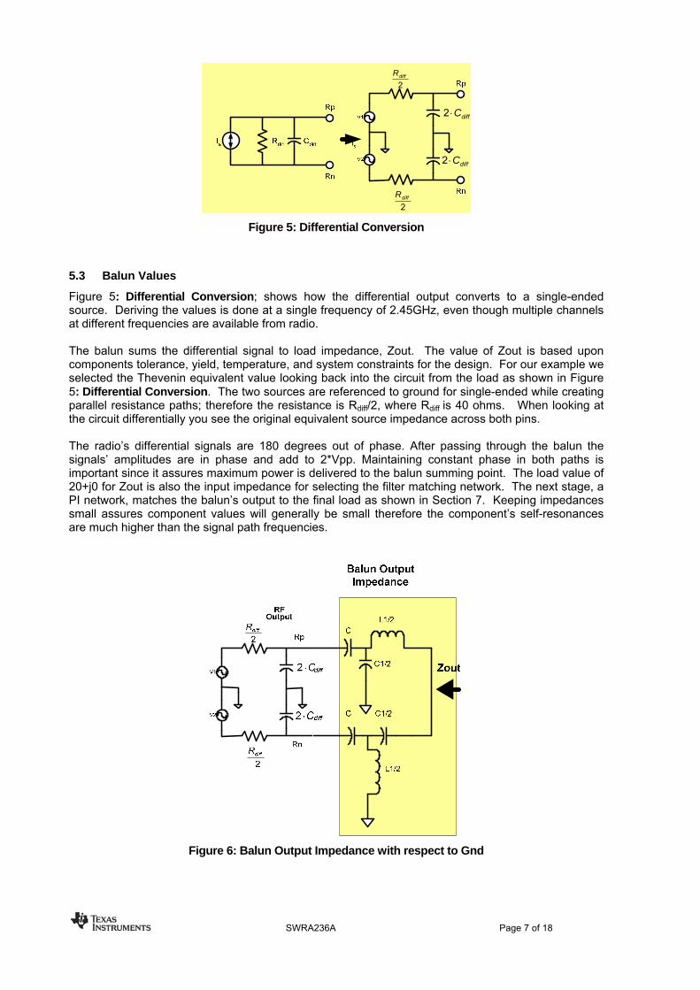
5.3 Balun Values
Figure 5: Differential Conversion; shows how the differential output converts to a single-ended source. Deriving the values is done at a single frequency of 2.45GHz, even though multiple channels at different frequencies are available from radio. The balun sums the differential signal to load impedance, Zout. The value of Zout is based upon components tolerance, yield, temperature, and system constraints for the design. For our example we selected the Thevenin equivalent value looking back into the circuit from the load as shown in Figure 5: Differential Conversion. The two sources are referenced to ground for single-ended while creating parallel resistance paths; therefore the resistance is Rdiff/2, where Rdiff is 40 ohms. When looking at the circuit differentially you see the original equivalent source impedance across both pins. The radio’s differential signals are 180 degrees out of phase. After passing through the balun the signals’ amplitudes are in phase and add to 2*Vpp. Maintaining constant phase in both paths is important since it assures maximum power is delivered to the balun summing point. The load value of 20+j0 for Zout is also the input impedance for selecting the filter matching network. The next stage, a PI network, matches the balun’s output to the final load as shown in Section 7. Keeping impedances small assures component values will generally be small therefore the component’s self-resonances are much higher than the signal path frequencies.
Figure 6: Balun Output Impedance with respect to Gnd
SWRA236A Page 7 of 18
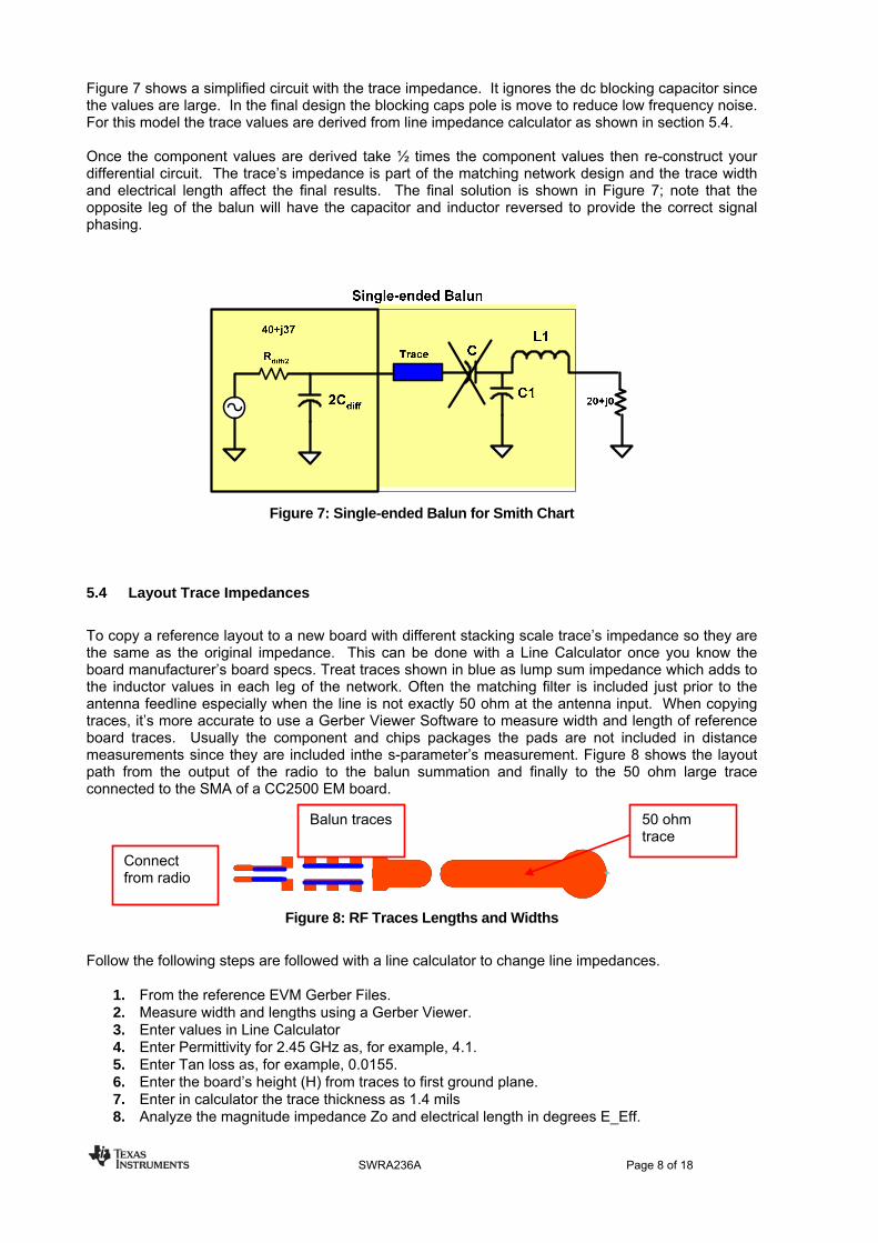
Figure 7 shows a simplified circuit with the trace impedance. It ignores the dc blocking capacitor since the values are large. In the final design the blocking caps pole is move to reduce low frequency noise. For this model the trace values are derived from line impedance calculator as shown in section 5.4. Once the component values are derived take ½ times the component values then re-construct your differential circuit. The trace’s impedance is part of the matching network design and the trace width and electrical length affect the final results. The final solution is shown in Figure 7; note that the opposite leg of the balun will have the capacitor and inductor reversed to provide the correct signal phasing.
Figure 7: Single-ended Balun for Smith Chart
5.4 Layout Trace Impedances
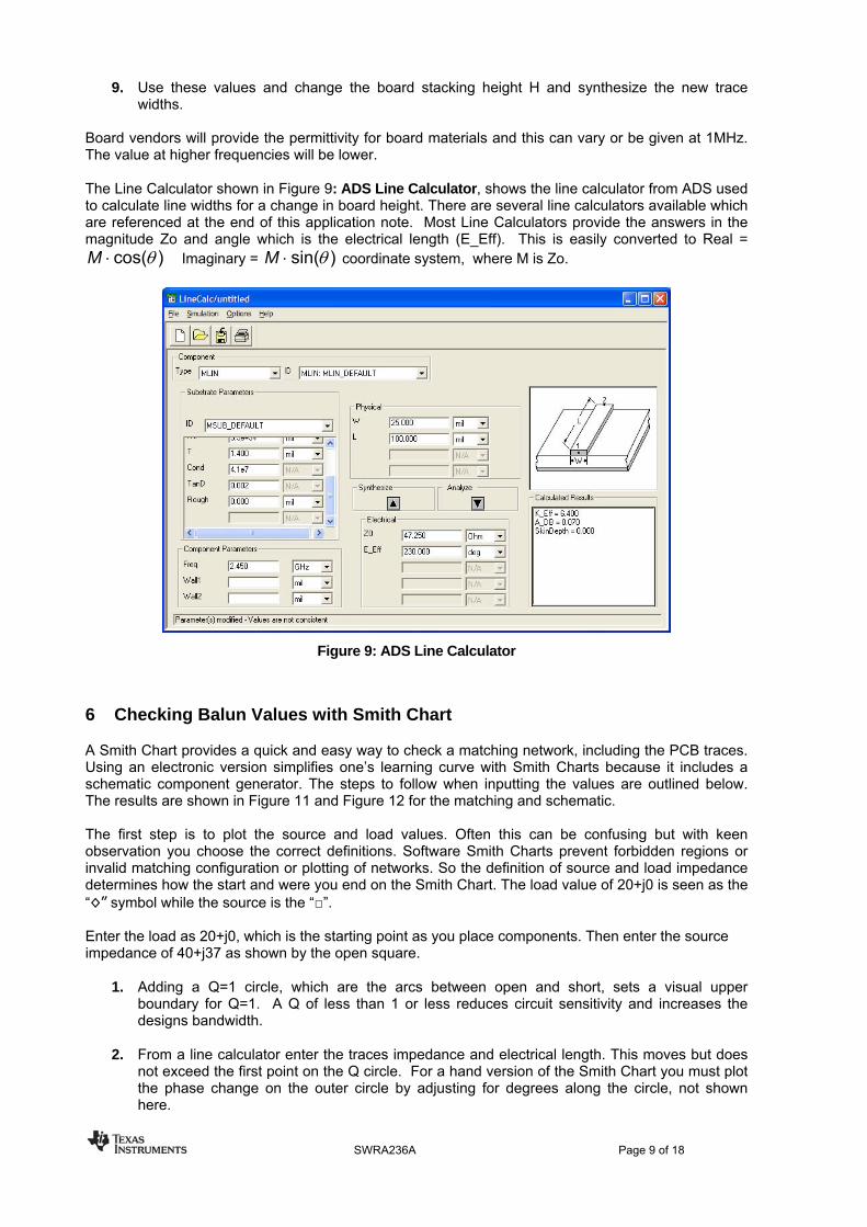
To copy a reference layout to a new board with different stacking scale trace’s impedance so they are the same as the original impedance. This can be done with a Line Calculator once you know the board manufacturer’s board specs. Treat traces shown in blue as lump sum impedance which adds to the inductor values in each leg of the network. Often the matching filter is included just prior to the antenna feedline especially when the line is not exactly 50 ohm at the antenna input. When copying traces, it’s more accurate to use a Gerber Viewer Software to measure width and length of reference board traces. Usually the component and chips packages the pads are not included in distance measurements since they are included inthe s-parameter’s measurement. Figure 8 shows the layout path from the output of the radio to the balun summation and finally to the 50 ohm large trace connected to the SMA of a CC2500 EM board.
Balun traces 50 ohm trace
Connect from radio
Figure 8: RF Traces Lengths and Widths
Follow the following steps are followed with a line calculator to change line impedances.
1. From the reference EVM Gerber Files. 2. Measure width and lengths using a Gerber Viewer. 3. Enter values in Line Calculator 4. Enter Permittivity for 2.45 GHz as, for example, 4.1. 5. Enter Tan loss as, for example, 0.0155. 6. Enter the board’s height (H) from traces to first ground plane. 7. Enter in calculator the trace thickness as 1.4 mils 8. Analyze the magnitude impedance Zo and electrical length in degrees E_Eff.
SWRA236A Page 8 of 18
9. Use these values and change the board stacking height H and synthesize the new trace widths.
Board vendors will provide the permittivity for board materials and this can vary or be given at 1MHz. The value at higher frequencies will be lower. The Line Calculator shown in Figure 9: ADS Line Calculator, shows the line calculator from ADS used to calculate line widths for a change in board height. There are several line calculators available which are referenced at the end of this application note. Most Line Calculators provide the answers in the magnitude Zo and angle which is the electrical length (E_Eff). This is easily converted to Real =
)cos(θ⋅M Imaginary = )sin(θ⋅M coordinate system, where M is Zo.
Figure 9: ADS Line Calculator
6 Checking Balun Values with Smith Chart
A Smith Chart provides a quick and easy way to check a matching network, including the PCB traces. Using an electronic version simplifies one’s learning curve with Smith Charts because it includes a schematic component generator. The steps to follow when inputting the values are outlined below. The results are shown in Figure 11 and Figure 12 for the matching and schematic. The first step is to plot the source and load values. Often this can be confusing but with keen observation you choose the correct definitions. Software Smith Charts prevent forbidden regions or invalid matching configuration or plotting of networks. So the definition of source and load impedance determines how the start and were you end on the Smith Chart. The load value of 20+j0 is seen as the “◊” symbol while the source is the “□”. Enter the load as 20+j0, which is the starting point as you place components. Then enter the source impedance of 40+j37 as shown by the open square.
1. Adding a Q=1 circle, which are the arcs between open and short, sets a visual upper boundary for Q=1. A Q of less than 1 or less reduces circuit sensitivity and increases the designs bandwidth.
2. From a line calculator enter the traces impedance and electrical length. This moves but does
not exceed the first point on the Q circle. For a hand version of the Smith Chart you must plot the phase change on the outer circle by adjusting for degrees along the circle, not shown here.
SWRA236A Page 9 of 18
3. Then add a capacitor to ground this moves the trace to the next point on the real impedance
axis.
4. Finally placing a series inductor moves the line to the source impedance of 40+j37. This indicates we have the correct values and trace lengths for our layout.
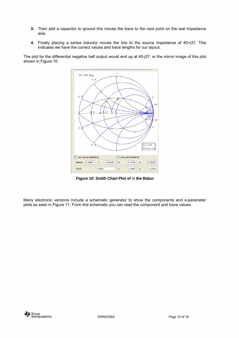
The plot for the differential negative half output would end up at 40-j37, or the mirror image of this plot shown in Figure 10.
Figure 10: Smith Chart Plot of ½ the Balun
Many electronic versions include a schematic generator to show the components and s-parameter plots as seen in Figure 11. From this schematic you can read the component and trace values.
SWRA236A Page 10 of 18

Figure 11: Schematics of Components and Total Trace Length
7 Pi Matching Filter and 50 Ohm Line
The Pi Matching low pass filter can also be checked for how well it matches the impedance of 20+j0 to the antenna load of 50+j0. Figure 12 includes the PCB traces connected to the output at C3. Changing the board stacking height changes the trace’s width-to-height ratio consequently the impedance.
SMA
Pi Network
50L2
C2 C3
20
Figure 12: Pi Network Schematic with 50 Ohm Trace
Using the Smith Chart to validate or derive the values for the filter network is done as outlined in the Section 6. Now the source load is 50 ohms and the source is 20. The results are shown in Figure 13.
SWRA236A Page 11 of 18
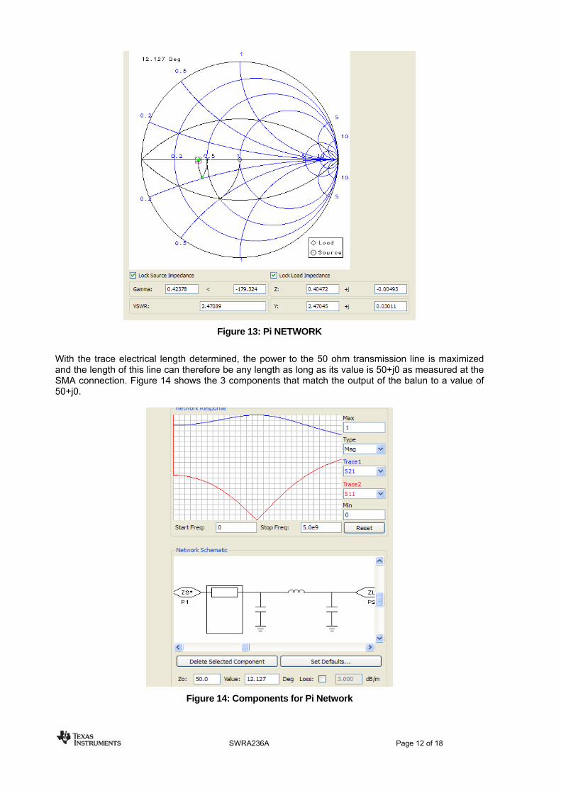
Figure 13: Pi NETWORK
With the trace electrical length determined, the power to the 50 ohm transmission line is maximized and the length of this line can therefore be any length as long as its value is 50+j0 as measured at the SMA connection. Figure 14 shows the 3 components that match the output of the balun to a value of 50+j0.
Figure 14: Components for Pi Network
SWRA236A Page 12 of 18

8 Software Simulation Results
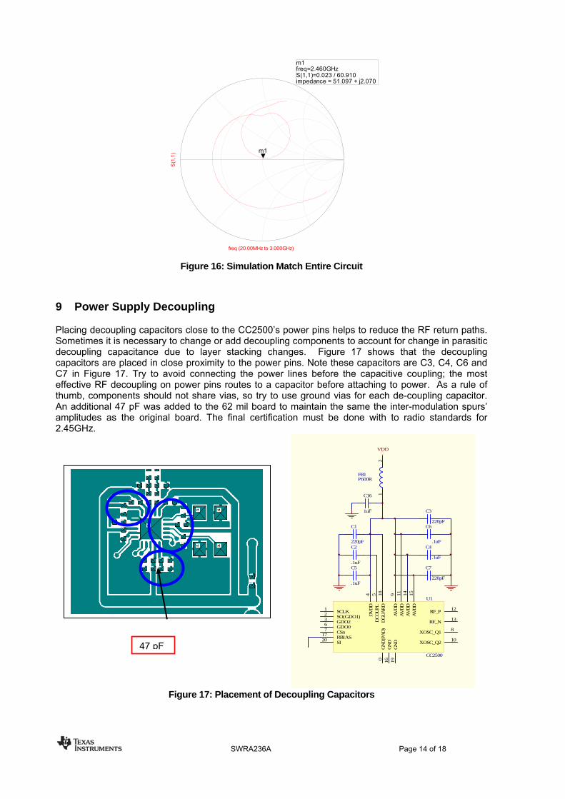
Smith Charts produce reasonably accurate results when plotting a tested design. But if the design happens to be new and doesn’t include the effects due to magnetic fringing a small error occurs in the final design. This effectively makes the lines appear longer and wider than their physical lengths. When copying the traces from reference designs there is no problem because the original traces account for this magnetic effect. Traces due to fringing vary in length and width from 5 – 8 %, so one is left to derive the correct line lengths. One way is to use 3-D simulation software. The simulation program shows the impedance results of the traces and components for the RF balun and filter in Figure 15. The simulator also has the ability to plot additional parameters such as S22, S21 and S11 and can calculate worse case performance. Figure 16 provides a plot of S11 looking into the filter/balun with a load set to the assumed output impedance of the CC2500, or 80-j74. The simulation of Figure 15 shows correlation to the final board’s measurement results in Figure 20. One should note that there always exist small differences between modelling and measurement, since it is difficult to have an exact match due to parasitic components. This can be due to measurements or parasitic components that are not included in the models or lab measurements.
SP_DiffSP_Diff1
Z2=80-74*jZ1=50+0*jNumPoints=1000Stop=3 GHzStart=20 MHz
- -
Netw ork Analyzer w ith Ungrounded Ports
+ +
21
GRM15C6Value="1.5[pF]"
MLINTL6
L=325 milW=w idth mil
GRM15C5Value="1.5[pF]"
GRM15C4Value="1[pF]"
LQG15L1Value="1.2[nH]"
GRM15C3Value="1[pF]"
VIAFCV2
T=1.4 milH=height milD=14.75 mil
VIAFCV1
T=1.4 milH=height milD=14.75 mil
LQG15L3Value="1.2[nH]"
LQG15L2Value="1.2[nH]"
MLINTL5
L=Len1 milW=45.0 mil
MCURVE2Curve2
Radius=Rad milW=w id mil
MCURVE2Curve1
Radius=Rad milW=w id mil
VIAFCV4
T=1.4 milH=height mil
MLINTL4
L=Len milW=8 mil
MLINTL2
L=Len milW=8 mil
MCLINCLin1
L=110 milS=10 milW=8 mil
VIAFCV3
T=1.4 milH=height mil
GRM15C1Value="100[pF]"
GRM15C2Value="100[pF]"
MLINTL1
L=Len milW=8 mil
MLINTL3
L=Len milW=8 mil
Figure 15: ADS Simulation Schematic
SWRA236A Page 13 of 18
freq (20.00MHz to 3.000GHz)
S(1
,1) m1
m1freq=S(1,1)=0.023 / 60.910impedance = 51.097 + j2.070
2.460GHz
Figure 16: Simulation Match Entire Circuit
9 Power Supply Decoupling
Placing decoupling capacitors close to the CC2500’s power pins helps to reduce the RF return paths. Sometimes it is necessary to change or add decoupling components to account for change in parasitic decoupling capacitance due to layer stacking changes. Figure 17 shows that the decoupling capacitors are placed in close proximity to the power pins. Note these capacitors are C3, C4, C6 and C7 in Figure 17. Try to avoid connecting the power lines before the capacitive coupling; the most effective RF decoupling on power pins routes to a capacitor before attaching to power. As a rule of thumb, components should not share vias, so try to use ground vias for each de-coupling capacitor. An additional 47 pF was added to the 62 mil board to maintain the same the inter-modulation spurs’ amplitudes as the original board. The final certification must be done with to radio standards for 2.45GHz.
SCLK1
SO(GDO1)2 DV
DD
4
DC
OU
PL5
XOSC_Q1 8
AV
DD
9
XOSC_Q2 10
GDO23
CSn7
RF_P 12
RF_N 13
AV
DD
11
AV
DD
14
RBIAS17
DG
UA
RD
18
SI20
GN
D(P
AD
)0
GDO06
AV
DD
15
GN
D16
GN
D19
U1
CC2500
C1
220pF
C5
.1uF
C4
.1uF
C7
220pF
12
FB1P600R
VDD
C6
.1uF
C16
1uF
C2
.1uF
C3
220pF
47 pF
Figure 17: Placement of Decoupling Capacitors
SWRA236A Page 14 of 18

10 Lab Measurements
10.1 Balun / Matching Network Measurements
Measurements assure that the design is operating correctly. Placing the Radio in RX mode and connecting a VNA to the antenna port (Figure 18) allows one to plot S11 for the balun and filter matching network. Make sure the VNA power output is turned down to -30 or -40 dBm so not to saturate the LNA and change its input impedance.
Figure 18: Measuring S11
From the Smith Charts in Figure 19 and Figure 20 the impedance is plotted as seen at the antenna port. The target value is 50+j0 at 2.45GHz. The original board plot in Figure 19 shows the impedance 41.21+j11 and is well within VSWR circle of 2. But since this is lower in value from the ideal 50 ohms, the power transmitted to the antenna is slightly low due to the reflected voltage from the mismatch. The closer the match is to the antenna impedance an improvement in the system efficiency occurs. This would compare better to the simulation if the layout was copied exactly and simulated; instead the simulation is a lumped-sum result, and therefore a slight difference is observed.
Figure 19: 31 mil, Stacking, Impedance of EVM Measured at Antenna SMA
SWRA236A Page 15 of 18
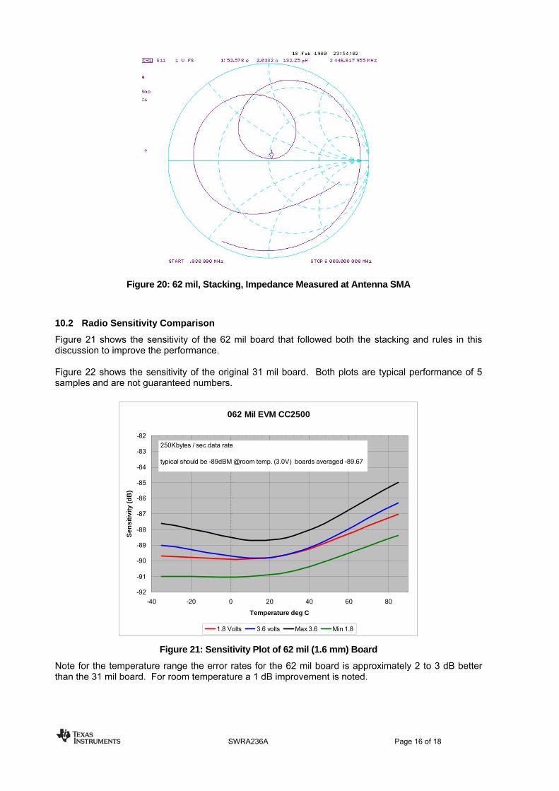
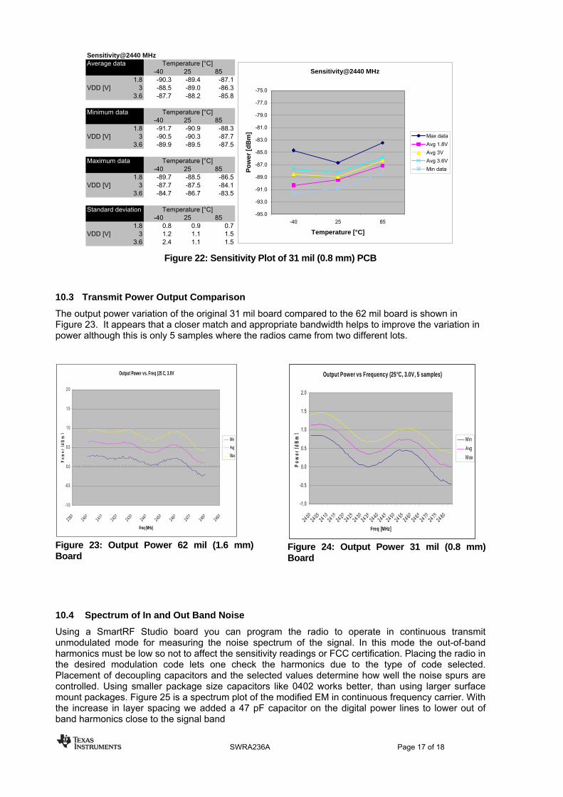
Figure 20: 62 mil, Stacking, Impedance Measured at Antenna SMA
10.2 Radio Sensitivity Comparison
Figure 21 shows the sensitivity of the 62 mil board that followed both the stacking and rules in this discussion to improve the performance. Figure 22 shows the sensitivity of the original 31 mil board. Both plots are typical performance of 5 samples and are not guaranteed numbers.
062 Mil EVM CC2500
-92
-91
-90
-89
-88
-87
-86
-85
-84
-83
-82
-40 -20 0 20 40 60 80
Temperature deg C
Sens
itivi
ty (d
B)
1.8 Volts 3.6 volts Max 3.6 Min 1.8
250Kbytes / sec data rate
typical should be -89dBM @room temp. (3.0V) boards averaged -89.67
Figure 21: Sensitivity Plot of 62 mil (1.6 mm) Board
Note for the temperature range the error rates for the 62 mil board is approximately 2 to 3 dB better than the 31 mil board. For room temperature a 1 dB improvement is noted.
SWRA236A Page 16 of 18
Sensitivity@2440 MHzAverage data Temperature [°C]
-40 25 851.8 -90.3 -89.4 -87.1
VDD [V] 3 -88.5 -89.0 -86.33.6 -87.7 -88.2 -85.8
Minimum data Temperature [°C]-40 25 85
1.8 -91.7 -90.9 -88.3VDD [V] 3 -90.5 -90.3 -87.7
3.6 -89.9 -89.5 -87.5
Maximum data Temperature [°C]-40 25 85
1.8 -89.7 -88.5 -86.5VDD [V] 3 -87.7 -87.5 -84.1
3.6 -84.7 -86.7 -83.5
Standard deviation Temperature [°C]-40 25 85
1.8 0.8 0.9 0.7VDD [V] 3 1.2 1.1 1.5
3.6 2.4 1.1 1.5
Sensitivity@2440 MHz
-95.0
-93.0
-91.0
-89.0
-87.0
-85.0
-83.0
-81.0
-79.0
-77.0
-75.0
-40 25 85
Temperature [°C]
Pow
er [d
Bm
] Max dataAvg 1.8VAvg 3VAvg 3.6VMin data
Figure 22: Sensitivity Plot of 31 mil (0.8 mm) PCB
10.3 Transmit Power Output Comparison
The output power variation of the original 31 mil board compared to the 62 mil board is shown in Figure 23. It appears that a closer match and appropriate bandwidth helps to improve the variation in power although this is only 5 samples where the radios came from two different lots.
Output Power vs. Freq (25 C, 3.0V
-1.0
-0.5
0.0
0.5
1.0
1.5
2.0
23902400
24102420
24302440
24502460
24702480
2490
Freq (MHz)
Pow
er (d
Bm
)
MinAvg
Max
Output Power vs Frequency (25°C, 3.0V, 5 samples)
-1.0
-0.5
0.0
0.5
1.0
1.5
2.0
24 0024 05
24 1024 15
24 2024 25
24 3024 35
24 4024 45
24 5024 55
24 6024 65
24 7024 75
24 80
Freq [MHz]
Pow
er [d
Bm
]
MinAvgMax
Figure 23: Output Power 62 mil (1.6 mm) Board
Figure 24: Output Power 31 mil (0.8 mm) Board
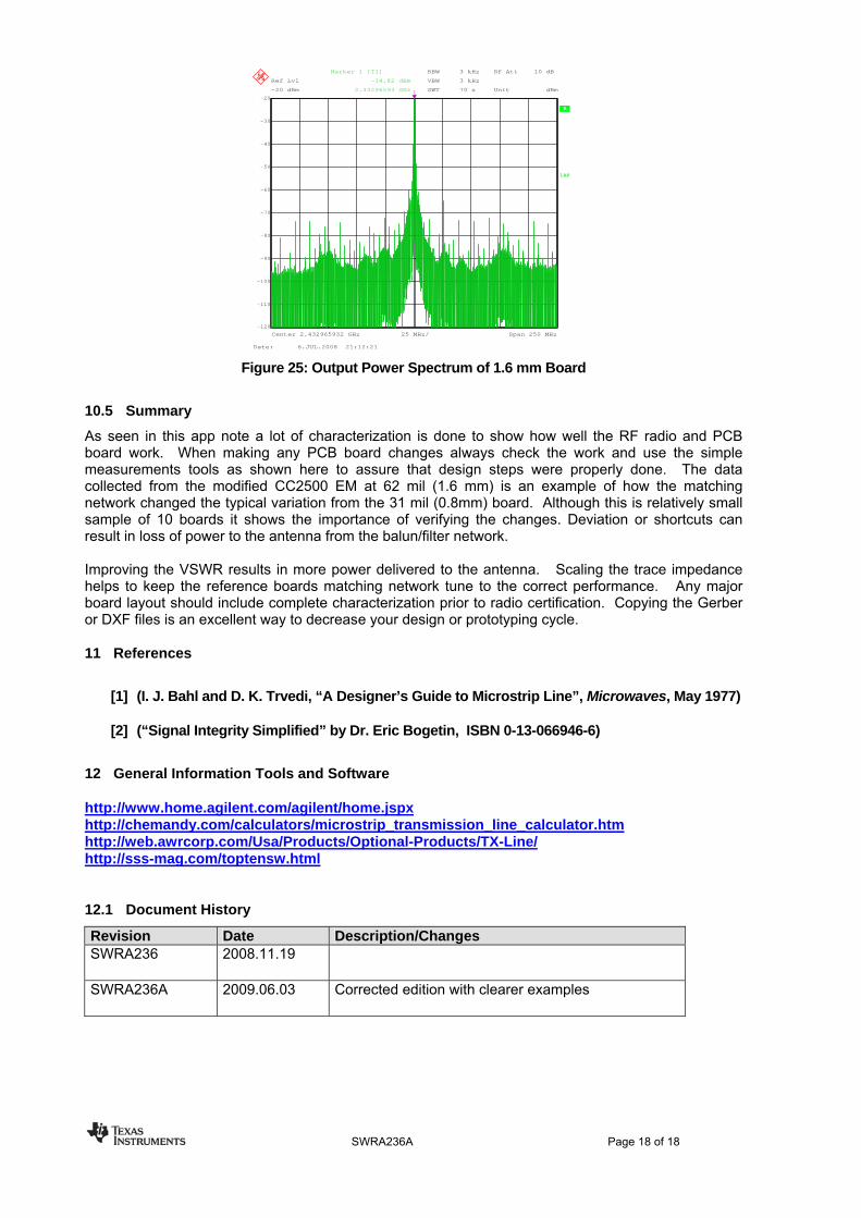
10.4 Spectrum of In and Out Band Noise
Using a SmartRF Studio board you can program the radio to operate in continuous transmit unmodulated mode for measuring the noise spectrum of the signal. In this mode the out-of-band harmonics must be low so not to affect the sensitivity readings or FCC certification. Placing the radio in the desired modulation code lets one check the harmonics due to the type of code selected. Placement of decoupling capacitors and the selected values determine how well the noise spurs are controlled. Using smaller package size capacitors like 0402 works better, than using larger surface mount packages. Figure 25 is a spectrum plot of the modified EM in continuous frequency carrier. With the increase in layer spacing we added a 47 pF capacitor on the digital power lines to lower out of band harmonics close to the signal band
SWRA236A Page 17 of 18
SWRA236A Page 18 of 18
Ref Lvl
-20 dBm
Ref Lvl
-20 dBm
RBW 3 kHz
VBW 3 kHz
SWT 70 s
RF Att 10 dB
25 MHz/Center 2.432965932 GHz Span 250 MHz
A
1AP
Unit dBm
-110
-100
-90
-80
-70
-60
-50
-40
-30
-120
-201
Marker 1 [T1]
-14.82 dBm
2.43296593 GHz
Date: 6.JUL.2008 21:12:21 Figure 25: Output Power Spectrum of 1.6 mm Board
10.5 Summary
As seen in this app note a lot of characterization is done to show how well the RF radio and PCB board work. When making any PCB board changes always check the work and use the simple measurements tools as shown here to assure that design steps were properly done. The data collected from the modified CC2500 EM at 62 mil (1.6 mm) is an example of how the matching network changed the typical variation from the 31 mil (0.8mm) board. Although this is relatively small sample of 10 boards it shows the importance of verifying the changes. Deviation or shortcuts can result in loss of power to the antenna from the balun/filter network. Improving the VSWR results in more power delivered to the antenna. Scaling the trace impedance helps to keep the reference boards matching network tune to the correct performance. Any major board layout should include complete characterization prior to radio certification. Copying the Gerber or DXF files is an excellent way to decrease your design or prototyping cycle. 11 References
[1] (I. J. Bahl and D. K. Trvedi, “A Designer’s Guide to Microstrip Line”, Microwaves, May 1977)
[2] (“Signal Integrity Simplified” by Dr. Eric Bogetin, ISBN 0-13-066946-6)
12 General Information Tools and Software
http://www.home.agilent.com/agilent/home.jspx http://chemandy.com/calculators/microstrip_transmission_line_calculator.htm http://web.awrcorp.com/Usa/Products/Optional-Products/TX-Line/ http://sss-mag.com/toptensw.html
12.1 Document History
Revision Date Description/Changes SWRA236 2008.11.19
SWRA236A 2009.06.03 Corrected edition with clearer examples

IMPORTANT NOTICETexas Instruments Incorporated and its subsidiaries (TI) reserve the right to make corrections, modifications, enhancements, improvements,and other changes to its products and services at any time and to discontinue any product or service without notice. Customers shouldobtain the latest relevant information before placing orders and should verify that such information is current and complete. All products aresold subject to TI’s terms and conditions of sale supplied at the time of order acknowledgment.TI warrants performance of its hardware products to the specifications applicable at the time of sale in accordance with TI’s standardwarranty. Testing and other quality control techniques are used to the extent TI deems necessary to support this warranty. Except wheremandated by government requirements, testing of all parameters of each product is not necessarily performed.TI assumes no liability for applications assistance or customer product design. Customers are responsible for their products andapplications using TI components. To minimize the risks associated with customer products and applications, customers should provideadequate design and operating safeguards.TI does not warrant or represent that any license, either express or implied, is granted under any TI patent right, copyright, mask work right,or other TI intellectual property right relating to any combination, machine, or process in which TI products or services are used. Informationpublished by TI regarding third-party products or services does not constitute a license from TI to use such products or services or awarranty or endorsement thereof. Use of such information may require a license from a third party under the patents or other intellectualproperty of the third party, or a license from TI under the patents or other intellectual property of TI.Reproduction of TI information in TI data books or data sheets is permissible only if reproduction is without alteration and is accompaniedby all associated warranties, conditions, limitations, and notices. Reproduction of this information with alteration is an unfair and deceptivebusiness practice. TI is not responsible or liable for such altered documentation. Information of third parties may be subject to additionalrestrictions.Resale of TI products or services with statements different from or beyond the parameters stated by TI for that product or service voids allexpress and any implied warranties for the associated TI product or service and is an unfair and deceptive business practice. TI is notresponsible or liable for any such statements.TI products are not authorized for use in safety-critical applications (such as life support) where a failure of the TI product would reasonablybe expected to cause severe personal injury or death, unless officers of the parties have executed an agreement specifically governingsuch use. Buyers represent that they have all necessary expertise in the safety and regulatory ramifications of their applications, andacknowledge and agree that they are solely responsible for all legal, regulatory and safety-related requirements concerning their productsand any use of TI products in such safety-critical applications, notwithstanding any applications-related information or support that may beprovided by TI. Further, Buyers must fully indemnify TI and its representatives against any damages arising out of the use of TI products insuch safety-critical applications.TI products are neither designed nor intended for use in military/aerospace applications or environments unless the TI products arespecifically designated by TI as military-grade or "enhanced plastic." Only products designated by TI as military-grade meet militaryspecifications. Buyers acknowledge and agree that any such use of TI products which TI has not designated as military-grade is solely atthe Buyer's risk, and that they are solely responsible for compliance with all legal and regulatory requirements in connection with such use.TI products are neither designed nor intended for use in automotive applications or environments unless the specific TI products aredesignated by TI as compliant with ISO/TS 16949 requirements. Buyers acknowledge and agree that, if they use any non-designatedproducts in automotive applications, TI will not be responsible for any failure to meet such requirements.Following are URLs where you can obtain information on other Texas Instruments products and application solutions:Products ApplicationsAmplifiers amplifier.ti.com Audio www.ti.com/audioData Converters dataconverter.ti.com Automotive www.ti.com/automotiveDLP® Products www.dlp.com Broadband www.ti.com/broadbandDSP dsp.ti.com Digital Control www.ti.com/digitalcontrolClocks and Timers www.ti.com/clocks Medical www.ti.com/medicalInterface interface.ti.com Military www.ti.com/militaryLogic logic.ti.com Optical Networking www.ti.com/opticalnetworkPower Mgmt power.ti.com Security www.ti.com/securityMicrocontrollers microcontroller.ti.com Telephony www.ti.com/telephonyRFID www.ti-rfid.com Video & Imaging www.ti.com/videoRF/IF and ZigBee® Solutions www.ti.com/lprf Wireless www.ti.com/wireless
Mailing Address: Texas Instruments, Post Office Box 655303, Dallas, Texas 75265Copyright © 2009, Texas Instruments Incorporated