an ultrathin graphite based absorber for wearable applications
TRANSCRIPT

An Ultrathin Graphite Based Absorber for WearableApplicationsAvinash ( [email protected] )
BIT Mesra: Birla Institute of Technology https://orcid.org/0000-0003-1290-0869Nisha Gupta
BIT Mesra: Birla Institute of Technology
Research Article
Keywords: Frequency selective surface, Microwave absorber, Ultrathin, Graphite, Flexible substrate
Posted Date: June 3rd, 2021
DOI: https://doi.org/10.21203/rs.3.rs-480007/v1
License: This work is licensed under a Creative Commons Attribution 4.0 International License. Read Full License

1
An Ultrathin Graphite Based Absorber for Wearable Applications
Avinash 1, Nisha Gupta2
1Department of Electronics and Communication Engineering, Birla Institute of
Technology, Mesra, Ranchi-835215, India
2Department of Electronics and Communication Engineering, Birla Institute of
Technology, Mesra, Ranchi-835215, India
Abstract
In this paper, a low-cost, flexible, ultrathin absorber comprising a simple square patch-
shaped frequency selective surface (FSS) is proposed for wearable applications. The FSS
based absorbing structure contains periodic graphite patch pattern placed on a thin paper
substrate, and backed with a copper foil-based ground plane. The dimension and
periodicity of the unit cell are 0.31𝜆0 and 0.36𝜆0 respectively, while the thickness of the
absorber is approximately 𝜆0/85, where 𝜆0 is the wavelength of free space at 10 GHz. The
characteristics of the FSS absorber is optimized in terms of unit cell periodicity, and
dielectric substrate height using a full-wave high frequency structure simulator software
(HFSS). The effects of the parameters are also examined using equivalent circuit approach.
The proposed absorber shows insensitivity towards the angle of incidence as well as angle
of polarization. Finally, a prototype model is fabricated, measured, and validated with
simulation results. A good agreement is depicted between simulated and experimental
models. The proposed absorber finds application in the field of wearable electronics,
medical, and automotive applications for effective mitigation of the EMI.
Keywords
Frequency selective surface, Microwave absorber, Ultrathin, Graphite, Flexible substrate.

2
1. Introduction
In the present wireless communication scenario, due to tremendous increase in the wireless
devices, the environment is full of electromagnetic (EM) pollution generated by different
source of EM wave. Hence, the issues of electromagnetic interference (EMI), and
electromagnetic compatibility (EMC) need more attention as both generating interference
to others and also working satisfactorily in the EM environment are equally important.
Among the two techniques of handling interference such as use of metallic barrier or use
of EM absorbers, the later one employing light-weight flexible structure is highly preferred
due to its sole purpose to absorb EMI unlike the metallic rigid structure which only diverts
the EMI to other direction. An EM absorber is mostly a periodic array of metallic patterns
printed over a dielectric sheet backed with a ground plane. In contrast to the traditional
rigid dielectric sheets, selecting a flexible dielectric material such as paper makes the
absorber thin, flexible, and conformal, thus suitable for wearable applications.
Why Graphite?
The loss parameter of the substrate as well as that of the printed conducting material plays
an important role in realizing an effective thin absorber. Graphite being a low cost,
lightweight, electrical conducting material of low conductivity, high complex permittivity
may be preferred because it exhibits large dielectric loss owing to the high imaginary part
of its permittivity [1]. The traditional conducting material on the other hand are highly
conducting materials with low dielectric loss. Flexible EM absorbers can easily be realized
using graphite FSS periodic pattern of PGS from Panasonic is placed over a thin dielectric
sheet such as flexible paper. The PGS is a very lightweight and thin polymer sheet that
exhibits excellent mechanical strength, high flexibility, and very high thermal conductivity,
which makes it suitable for wearable outdoor applications. Flexible sheet can be easily cut
into desired shapes. Due to its high thermal conductivity, it is mostly used for managing
the heat in electronics circuitry. Moreover, the sheet resistance can easily be modified to
the desired value by changing the applied voltage bias, thus dictating its future application
in several tuneable device applications.

3
2. Related Works
Design of low cost, thin and conformal EM absorber is indeed a complicated task [2].
Selection of materials of both substrate as well as FSS pattern are equally important in
deciding the absorption characteristics of the EM absorber. Design of a thin lightweight
conformal absorber is still a challenge, and a large number of researchers have attempted
to overcome this challenge while designing the EM absorbers. The design of a resonant
Salisbury absorber with optimum resistive surface is presented in [3]. However, the
problem lies with the thickness of spacer between ground plane and resistive surface.
Among the various techniques employed to overcome thickness problem in designing the
EM absorber, use of lossy FSS technique [4], high impedance surface technique [5], circuit
analog absorber [6] are noteworthy. While the basic principle of realizing a thin EM
absorber is discussed in [7], a thin capacitive surface based absorber is explained in [8]. A
very thin, flexible pyrolytic graphite sheet (PGS) made from highly oriented graphite
polymer film is selected for the FSS in [9]. In the past graphite is also used in the design
of patch antennas where the conventional conducting patch is replaced by graphite patch
[1]. However, the high resistivity of the material leads to poor performance of the antenna
in terms of gain and radiation efficiency. On the other hand, high resistivity of the graphite
offers advantage in the design of absorber, where the high sheet resistance enhances the
absorption mechanism of the absorber. Use of graphite sheet alone for attenuating the
microwave radiation is also reported by some of the physicists [10-11]. In the present work,
instead of using graphite sheet alone for mitigating the EMI, it is used as a conducting
material for the design of the FSS patch. The design of a simple square graphite patch FSS
absorber is proposed in this work and based on the characteristics of the material and the
extensive simulation parameters, a scheme is proposed for realization of a thin EM
absorber at 10 GHz.
3. Design and Analysis of Absorber
The proposed absorber is different from a traditional absorber both in terms of material
and the fabrication process. Hence, instead of altogether proposing a new FSS patch design

4
to demonstrate the design and fabrication process, a well-known, and thoroughly
investigated square patch FSS is considered. Design and analysis of a square patch FSS
for its application as EM absorber is systematically explained in [5], [12], [13]. Fig.1
shows a unit cell of the proposed square patch array of PGS (conductivity, 𝜎 = 2 ×10⁶𝑆/𝑚) absorber of 0.025 mm thick FSS layer on the top of a dielectric layer. Two layers
of a paper sheet of thickness 0.177 mm ( 𝜀𝑟 = 2.2, 𝜹𝒕 = 0.05) is used as dielectric
substrate grounded on a copper foil with thickness 0.011 mm (conductivity, 𝜎 = 5.8 ×10⁷𝑆/𝑚).
Impedance matching of the EM wave (free space impedance) impinging on the surface of
the absorber with that of the absorber is the first and foremost criteria in the design of the
EM absorber. Moreover, this phenomenon can be very well explained by adopting the
equivalent circuit model of the absorber, where each layer of the absorber is depicted
clearly and perfect matching can be achieved by selecting specific set of FSS patch
parameters. The surface current distribution approach [14] is applied to draw the
equivalent circuit of the proposed absorber.
Fig.1 Unit cell of proposed absorber with dimensions (a) Top view: Periodicity of the
absorber, p = 10.9 mm, length of the square patch length, l = 9.3 mm (b) Isometric View
and (c) Side View, thickness of substrate, t = 0.354 mm

5
In Fig.2 The equivalent circuit model of the proposed absorber is presented where a series
RLC circuit represents the unit cell of the FSS. The impedance of the FSS, 𝑍𝐹𝑆𝑆 can be
represented as 𝑍𝐹𝑆𝑆 = 𝑅𝐹𝑆𝑆 + 𝑗𝜔𝐿𝐹𝑆𝑆 + 1𝑗𝜔𝐶𝐹𝑆𝑆 (1)
Where, 𝑅𝐹𝑆𝑆 , 𝐿𝐹𝑆𝑆, 𝐶𝐹𝑆𝑆 are the equivalent resistance, inductance and capacitance of the
FSS and ω is angular frequency of the incident EM wave.
Fig.2 Equivalent circuit of the unit cell of proposed absorber
Various techniques such as analytical and simulation-based approach [15-16], can be used
to extract equivalent circuit parameters of the proposed absorber. The extracted values of 𝑅𝐹𝑠𝑠𝑠, 𝐿𝐹𝑆𝑆, and 𝐶𝐹𝑆𝑆 are 1.19Ω, 0.165𝑛𝐻, and 0.377𝑝𝐹 respectively.
The impedance of a dielectric slab can be considered as piece of a transmission line with
input impedance 𝑍𝑑, and can be given as 𝑍𝑑 = 𝑍0 (𝑍𝐿+𝑗𝑍0 tan(𝛽𝑑)𝑍0+𝑗𝑍𝐿 tan(𝛽𝑑)) (2)
A highly conductive metal foil is used as a ground plane of the proposed absorber, which
also acts as a load for the dielectric slab. The impedance of a metal foil is almost equivalent
to zero, so in (2), 𝑍𝐿 ≈ 0, and impedance of a transmission line with a short-circuited load
is represented as 𝑍𝑑 = 𝑗𝑍0 tan(𝛽𝑑) (3)
Where, 𝑍0 is the intrinsic impedance, 𝛽 is phase constant and d is the thickness of dielectric
slab.
6
𝑍0 = √𝜇𝜀 = √𝜇𝑟𝜇0𝜀𝑟𝜀0 = 377√𝜀𝑟 and , 𝛽 = 𝜔√𝜇𝜀
The surface impedance, 𝑍𝑖𝑛 of the absorber is equivalent to the parallel connection between 𝑍𝐹𝑆𝑆 and 𝑍𝑑 as 𝑍𝑖𝑛 = 𝑍𝐹𝑆𝑆 ∥ 𝑍𝑑 (4)
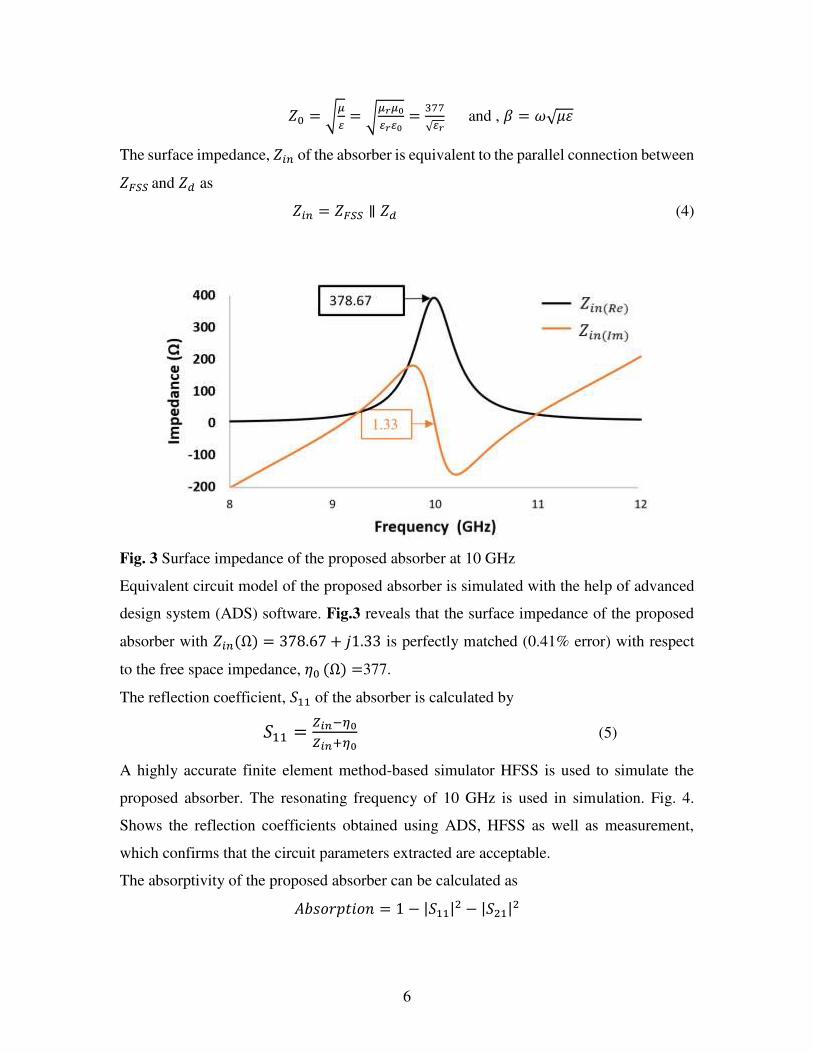
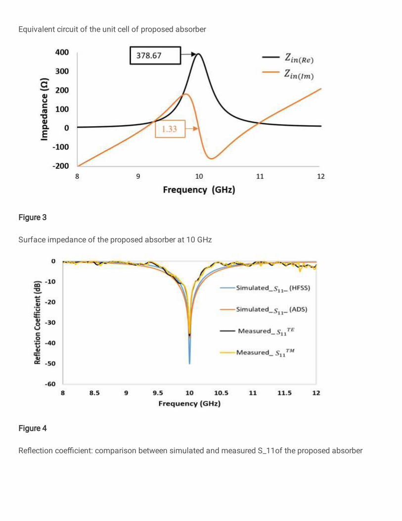
Fig. 3 Surface impedance of the proposed absorber at 10 GHz
Equivalent circuit model of the proposed absorber is simulated with the help of advanced
design system (ADS) software. Fig.3 reveals that the surface impedance of the proposed
absorber with 𝑍𝑖𝑛(Ω) = 378.67 + 𝑗1.33 is perfectly matched (0.41% error) with respect
to the free space impedance, 𝜂0 (Ω) =377.
The reflection coefficient, 𝑆11 of the absorber is calculated by 𝑆11 = 𝑍𝑖𝑛−𝜂0𝑍𝑖𝑛+𝜂0 (5)
A highly accurate finite element method-based simulator HFSS is used to simulate the
proposed absorber. The resonating frequency of 10 GHz is used in simulation. Fig. 4.
Shows the reflection coefficients obtained using ADS, HFSS as well as measurement,
which confirms that the circuit parameters extracted are acceptable.
The absorptivity of the proposed absorber can be calculated as 𝐴𝑏𝑠𝑜𝑟𝑝𝑡𝑖𝑜𝑛 = 1 − |𝑆11|2 − |𝑆21|2

7
The ground plane being a highly conductive material copper with thickness more than its
skin depth calculated at lowest frequency of X band, prohibits the transmission of the EM
wave completely. Hence, 𝑆21 ≈ 0 and absorption totally depends on the value of 𝑆11 as 𝐴𝑏𝑠𝑜𝑟𝑝𝑡𝑖𝑜𝑛 = 1 − |𝑆11|2
Fig.4 Reflection coefficient: comparison between simulated and measured 𝑆11of the
proposed absorber
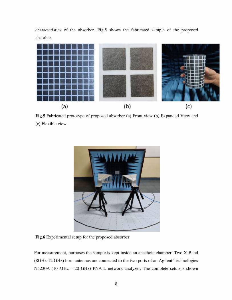
4. Experimental Results and Discussion
For verification of the proposed absorber, a prototype sample of 10 X 10 unit cell is
fabricated on a 110mm X 110mm planar paper with a thickness of 0.177 mm and two
sheets are pasted back to back to make a total thickness of 0.354mm. A copper foil of
thickness 0.011 mm is pasted on the back of the paper to act as a ground. The most
important part of the absorber, the FSS is fabricated with the available PGS EYGS121803
by Panasonic with dimensions 115 mm x 180 mm. A total of 100 graphite patches with
optimized dimension of 9.3 mm are cut manually with a detail knife. After cutting PGS,
the patches are pasted on the top of the substrate with adhesive tape manually. However,
during the PGS cutting and pasting process, accuracy and precision are given prime
importance, yet some errors are inevitable. A very thin lamination of the complete
absorber makes it work under all weather conditions, which hardly changes the
8
characteristics of the absorber. Fig.5 shows the fabricated sample of the proposed
absorber.
Fig.5 Fabricated prototype of proposed absorber (a) Front view (b) Expanded View and
(c) Flexible view
Fig.6 Experimental setup for the proposed absorber
For measurement, purposes the sample is kept inside an anechoic chamber. Two X-Band
(8GHz-12 GHz) horn antennas are connected to the two ports of an Agilent Technologies
N5230A (10 MHz – 20 GHz) PNA-L network analyzer. The complete setup is shown

9
in Fig.6 A distance of 1.5 m is maintained between sample and horn antenna to measure
the reflection coefficient for different angle polarization (φ), and incident angle (θ) varying
from 𝜑 = 0° to 90° and θ = 0° to 75° respectively. Moving average technique is applied
to smooth the measured result, was compared with the simulated one. Fig.4 indicates a
reasonable agreement between the simulated and measured results of the reflection
coefficient for normal incidence of TE and TM mode.
Fig.7 Simulated absorption, reflection and cross polarization of the proposed absorber
Fig.7 Shows simulated and measured magnitude of reflection, cross polarization and
absorption of the proposed absorber. Almost zero reflection, zero cross polarization, and
99.99% absorption are achieved in the proposed absorber.
To realize an absorber that behaves uniformly at any angle of polarization of EM wave,
the interaction between the electric field and the structure must be steady at all angles of
polarisation. Since the structure used in the FSS possess axial symmetry, the proposed
absorber is angularly stable. Fig.8(a) shows that absorption remains almost constant at
different polarisation angles (φ) which makes the proposed absorber polarization
insensitive. The proposed absorber is also studied for oblique incidence of TE- Mode.
Fig.8(b) shows that more than 80% absorption is achieved upto 60° angle of incidence
(𝜃).

10
Fig.8 Simulated absorption (a) for different angle of polarization φ and (b) for different
incident angle θ
At the moment when EM wave strikes on the surface of the absorber, instantly free charge
carriers distribute themselves and induce an electric field. Fig.9(a) shows surface current
distribution on the top surface of the proposed absorber at the resonant frequency which
exhibits that most of the current is distributed on the surface of conducting patch. This can
be easily explained based on the concept of skin effect. The confinement of the more
current towards the edges depends on the dielectric property of the substrate, frequency of
operation, and the discontinuity of the patch. Negligible displacement current also flows
through dielectric layer. Fig.9(b) shows electric field distribution of the proposed absorber.
Fig.9 Simulated plot of (a) surface current distribution (b) electric field distribution of the
proposed absorber at 10 GHz

11
Table 1: Comparison of various reported absorbers with proposed ultrathin absorber
Ref. 𝒇𝒓a (GHz) Substrate t b(mm) 𝜺𝒓c 𝜹𝒕d FSS Material Flexiblity
[17] 10.14 Fr4 1 4.3 0.02 Copper No
[18] 10 Rogers4003 0.508 3.38 0.0027 Copper No
[19] 10.8 Textile 1.2 1.8 0.12 Silver Conductive Ink Yes
[20] 9.5 Paper 1.19 3 0.05 Silver Conductive Ink Yes
[21] 11 PDMS 0.5 2.89 0.02 Silver Conductive Ink Yes
Proposed 10 Paper 0.354 2.2 0.05 PGS Yes a Resonating frequency b Thickness of substrate
c Relative permittivity of substrate d Loss tangent of substrate
Finally, the proposed FSS absorber is compared with the several other absorbers available
in the literature and their performance parameters are compared in the Table 1. As seen the
proposed absorber outperforms the other absorbers in terms of the thickness. Besides, a
simple fabrication technique is used to develop the prototype model. For the purpose of
mass production, a well-established screen-printing technology may be employed to realize
the proposed absorber, where graphite ink may be used in screen printing.
5. Conclusion
An ultra-thin, lightweight, flexible resonant absorber is realized using low cost and readily
available Panasonic graphite sheet, paper sheet, and copper foil. Electromagnetic
parameters of the proposed absorber are first converted to circuit parameter to derive the
equivalent circuit of the proposed absorber. The impedance matching of the proposed
absorber with free space impedance, shows almost zero reflection, and 99.99% absorption.
Also, the proposed absorber works perfectly for all angle of polarization and is hardly
influenced by the different angle of incidence. A comparison of the proposed absorber with
the previously reported absorber for X band application shows superiority of the absorber
in terms of thickness, which is achieved with the help of pyrolytic graphite sheet. The
proposed absorber is found to be suitable for wearable outdoor applications.
6. Declarations

12
Funding: This study was not funded by any one. Funding information is not applicable
and No funding was received.
Conflict of interests / Competing interests: The authors have no conflicts of interest to
declare that are relevant to the content of this articl
Availability of data and material: Work contained in this manuscript is original and
whenever I have used materials (data, theoretical analysis and text) from other sources, I
have given due credit to them by citing them in the text and giving their details in the
references.
Code availability: The work does not require any coding as the simulation software
package is used in the analysis.
Authors' contributions: The work contained in this manuscript is original. In this
manuscript a low-cost graphite based thin resonant electromagnetic absorber is proposed
for the wearable application. A comparison of the proposed absorber with the other existing
absorbers clearly shows its benefit in terms of thickness and cost.
References
1. Ansari, A., & Akhtar, M. J. (2017). Co/graphite based light weight microwave
absorber for electromagnetic shielding and stealth applications. Materials Research
Express, 4(1), 016304
2. Tirkey, M. M., & Gupta, N. (2019). Electromagnetic absorber design
challenges. IEEE Electromagnetic Compatibility Magazine, 8(1), 59-65.
3. Chambers, B. (1994). Optimum design of a Salisbury screen radar
absorber. Electronics Letters, 30(16), 1353-1354.

13
4. Silva, M. W. B., Campos, A. L. P. S., & Kretly, L. C. (2015). Design of thin
microwave absorbers using lossy frequency selective surfaces. Microwave and
Optical Technology Letters, 57(4), 928-933.
5. Costa, F., Monorchio, A., & Manara, G. (2010). Analysis and design of ultra thin
electromagnetic absorbers comprising resistively loaded high impedance
surfaces. IEEE Transactions on Antennas and Propagation, 58(5), 1551-1558.
6. Munk, B. A., Munk, P., & Pryor, J. (2007). On designing Jaumann and circuit
analog absorbers (CA absorbers) for oblique angle of incidence. IEEE Transactions
on Antennas and Propagation, 55(1), 186-193.
7. Tretyakov, S. (2016). Thin absorbers: operational principles and various
realizations. IEEE Electromagnetic Compatibility Magazine, 5(2), 61-66.
8. Han, Y., Che, W., Christopoulos, C., & Chang, Y. (2015). Investigation of thin and
broadband capacitive surface-based absorber by the impedance analysis
method. IEEE Transactions on Electromagnetic Compatibility, 57(1), 22-26.
9. https://www.farnell.com/datasheets/2244033.pdf
10. Wu, K. H., Cheng, K. F., Wang, J. C., & Chang, Y. C. (2017). Preparation of
magnetic expanded graphite with microwave absorption and infrared stealth
characteristics. Materials Express, 7(6), 500-508.
11. Borah, D., & Bhattacharyya, N. S. (2017). Design and development of expanded
graphite-based non-metallic and flexible metamaterial absorber for X-band
applications. Journal of Electronic Materials, 46(1), 226-232.
12. Luukkonen, O., Simovski, C., Granet, G., Goussetis, G., Lioubtchenko, D.,
Raisanen, A. V., & Tretyakov, S. A. (2008). Simple and accurate analytical model
of planar grids and high-impedance surfaces comprising metal strips or
patches. IEEE Transactions on Antennas and Propagation, 56(6), 1624-1632.
13. Firouzfar, A., Afsahi, M., & Orouji, A. A. (2019). Novel synthesis formulas to
design square patch frequency selective surface absorber based on equivalent
circuit model. International Journal of RF and Microwave Computer‐Aided
Engineering, 29(6), e21680.

14
14. Ghosh, S., & Srivastava, K. V. (2014). An equivalent circuit model of FSS-based
metamaterial absorber using coupled line theory. IEEE Antennas and Wireless
Propagation Letters, 14, 511-514.
15. Costa, F., Monorchio, A., & Manara, G. (2009, September). An equivalent-circuit
modeling of high impedance surfaces employing arbitrarily shaped FSS. In 2009
International Conference on Electromagnetics in Advanced Applications (pp. 852-
855). IEEE.
16. Sjöberg, D. (2008). Analysis of wave propagation in stratified structures using
circuit analogues, with application to electromagnetic absorbers. European journal
of physics, 29(4), 721.
17. Zhu, B., Wang, Z., Huang, C., Feng, Y., Zhao, J., & Jiang, T. (2010). Polarization
insensitive metamaterial absorber with wide incident angle. Progress In
Electromagnetics Research, 101, 231-239.
18. Liu, Y., De Flaviis, F., & Alexopoulos, N. G. (2008). A thin X-band microwave
absorber using a center shorted spiral medium. IEEE Antennas and Wireless
Propagation Letters, 8, 271-274.
19. Lee, D., Kim, H. K., & Lim, S. (2017). Textile metamaterial absorber using screen
printed channel logo. Microwave and Optical Technology Letters, 59(6), 1424-
1427.
20. Yoo, M., Kim, H. K., Kim, S., Tentzeris, M., & Lim, S. (2015). Silver nanoparticle-
based inkjet-printed metamaterial absorber on flexible paper. IEEE Antennas and
Wireless Propagation Letters, 14, 1718-1721.
21. Jeong, H., & Lim, S. (2017). A stretchable electromagnetic absorber fabricated
using screen printing technology. Sensors, 17(5), 1175.

Figures
Figure 1
Unit cell of proposed absorber with dimensions (a) Top view: Periodicity of the absorber, p = 10.9 mm,length of the square patch length, l = 9.3 mm (b) Isometric View and (c) Side View, thickness of substrate,t = 0.354 mm
Figure 2
Equivalent circuit of the unit cell of proposed absorber
Figure 3
Surface impedance of the proposed absorber at 10 GHz
Figure 4
Reection coecient: comparison between simulated and measured S_11of the proposed absorber

Figure 5
Fabricated prototype of proposed absorber (a) Front view (b) Expanded View and (c) Flexible view
Figure 6
Experimental setup for the proposed absorber

Figure 7
Simulated absorption, reection and cross polarization of the proposed absorber
Figure 8
Simulated absorption (a) for different angle of polarization φ and (b) for different incident angle θ

Figure 9
Simulated plot of (a) surface current distribution (b) electric eld distribution of the proposed absorber at10 GHz