an rf (r)ms power detector in standard cmos.€¦ · an rf (r)ms power detector in standard cmos....
TRANSCRIPT

An RF (R)MS Power Detector inStandard CMOS.
MSc. Thesisby Ing. F.H.J. van der Aa (s0042234)
Report number: 67.3173July 18, 2006
University of TwenteFaculty of Electrical Engineering,
Mathematics & Computer Science (EEMCS)Chair of Integrated Circuit Design (ICD)
P. O. Box 2177500 AE Enschede
The Netherlands
National Semiconductor B.V.Delftechpark 19
2628 XJ DelftThe Netherlands
Committee of supervisors:Nauta, Prof. Dr. Ir. B. (University of Twente)
Annema, Dr. Ir. A.J. (University of Twente)Eschauzier, Dr. Ir. R.G.H. (National Semiconductor)
Kouwenhoven, Dr. Ir. M.H.L. (National Semiconductor)


Abstract
This Master thesis describes the research towards the integration of RF powerdetectors for 3G cellular phones and base stations in CMOS technology1. Itis a feasibility study with the emphasis on the identification of fundamen-tal limitations of CMOS (particularly CMOS9) and of a number of squaringcircuits for this specific application, rather than to meet the target specifica-tions.
This report starts with a literature study about this kind of applicationand the possibilities to detect such signals, followed by a description of all re-quirements and specifications. Afterwards, the focus is on squaring circuits,which are needed for an RF (R)MS power detector, four kinds of squaringcircuits are compared. A new RMS circuit is designed (based on the multi-tail circuit): the feedback RMS detector circuit. In simulations, this circuitcomplies with all specifications.
In conclusion, it appears to be feasible to design RF (R)MS power detec-tors in standard CMOS.
1The project is defined by National Semiconductor in Delft and is carried out at theUniversity of Twente in Enschede.


Contents
List of Figures vi
List of Tables vii
List of Acronyms ix
1 Introduction 1
2 RF power measurement 3
2.1 Power control loop . . . . . . . . . . . . . . . . . . . . . . . . 4
2.1.1 Digital control in loop . . . . . . . . . . . . . . . . . . 5
2.2 Definition of RMS . . . . . . . . . . . . . . . . . . . . . . . . . 6
2.3 Traditional power measurement . . . . . . . . . . . . . . . . . 6
2.3.1 Absolute power levels . . . . . . . . . . . . . . . . . . . 6
2.3.2 PAR . . . . . . . . . . . . . . . . . . . . . . . . . . . . 7
3 Directional coupler 11
4 Power detectors 15
4.1 Parameters . . . . . . . . . . . . . . . . . . . . . . . . . . . . 16
4.2 Peak detection . . . . . . . . . . . . . . . . . . . . . . . . . . 17
4.2.1 Diodes . . . . . . . . . . . . . . . . . . . . . . . . . . . 17
4.2.2 Bipolar transistors . . . . . . . . . . . . . . . . . . . . 19
4.3 Logarithmic detection . . . . . . . . . . . . . . . . . . . . . . 21
4.4 True RMS detection . . . . . . . . . . . . . . . . . . . . . . . 23
4.4.1 Thermal detection . . . . . . . . . . . . . . . . . . . . 23
4.4.2 Log-antilog detection . . . . . . . . . . . . . . . . . . . 24
4.4.3 Squaring cell detection . . . . . . . . . . . . . . . . . . 26
4.5 Conclusion . . . . . . . . . . . . . . . . . . . . . . . . . . . . . 31
i

CONTENTS
5 Requirements 33
5.1 Power detector requirements . . . . . . . . . . . . . . . . . . . 335.1.1 Frequency range . . . . . . . . . . . . . . . . . . . . . . 33
5.1.2 Absolute power accuracy . . . . . . . . . . . . . . . . . 34
5.1.3 Relative power accuracy . . . . . . . . . . . . . . . . . 36
5.1.4 Output power transient response . . . . . . . . . . . . 375.1.5 Operating temperature . . . . . . . . . . . . . . . . . . 37
5.1.6 Power supply . . . . . . . . . . . . . . . . . . . . . . . 37
5.1.7 Summary of requirements . . . . . . . . . . . . . . . . 385.2 Squaring cell requirements . . . . . . . . . . . . . . . . . . . . 39
5.2.1 Exact MS . . . . . . . . . . . . . . . . . . . . . . . . . 39
5.2.2 Non-exact MS . . . . . . . . . . . . . . . . . . . . . . . 41
6 MOS squaring cells 45
6.1 Setting up the simulations . . . . . . . . . . . . . . . . . . . . 476.2 Translinear . . . . . . . . . . . . . . . . . . . . . . . . . . . . 48
6.3 Transistor-size unbalance technique . . . . . . . . . . . . . . . 51
6.4 Multitail . . . . . . . . . . . . . . . . . . . . . . . . . . . . . . 54
6.5 DC floating voltage sources . . . . . . . . . . . . . . . . . . . 576.6 Comparison . . . . . . . . . . . . . . . . . . . . . . . . . . . . 59
6.7 Adding non-linearities . . . . . . . . . . . . . . . . . . . . . . 60
6.7.1 Bias current via mirror . . . . . . . . . . . . . . . . . . 606.7.2 Output current via mirror . . . . . . . . . . . . . . . . 61
6.8 Second order effects . . . . . . . . . . . . . . . . . . . . . . . . 62
6.8.1 Body effect . . . . . . . . . . . . . . . . . . . . . . . . 64
6.8.2 Channel length modulation . . . . . . . . . . . . . . . 646.8.3 Mobility degradation . . . . . . . . . . . . . . . . . . . 64
6.8.4 Subthreshold conduction . . . . . . . . . . . . . . . . . 66
6.9 Feedback loop . . . . . . . . . . . . . . . . . . . . . . . . . . . 676.10 Feedback RMS detector circuit . . . . . . . . . . . . . . . . . 69
7 Results 717.1 Linearity . . . . . . . . . . . . . . . . . . . . . . . . . . . . . . 72
7.2 Operating frequency . . . . . . . . . . . . . . . . . . . . . . . 74
7.3 Dynamic range . . . . . . . . . . . . . . . . . . . . . . . . . . 757.4 Supply voltage . . . . . . . . . . . . . . . . . . . . . . . . . . 77
7.5 Operating temperature . . . . . . . . . . . . . . . . . . . . . . 79
7.5.1 Supply current . . . . . . . . . . . . . . . . . . . . . . 79
7.6 Non-quasi-static effects . . . . . . . . . . . . . . . . . . . . . . 827.7 Mismatch . . . . . . . . . . . . . . . . . . . . . . . . . . . . . 83
ii Master Thesis

CONTENTS
8 Conclusion 89
9 Recommendations 91
A Available RMS detectors 93A.1 AD8362 . . . . . . . . . . . . . . . . . . . . . . . . . . . . . . 93
B Taylor series of some common functions 95
C Basic level 1 MOS model (SpectreHDL) 97
D Final Kimura (MT)-based circuit 101
E Bipolar squaring cells 103E.1 Triplet multi-tanh squaring cell . . . . . . . . . . . . . . . . . 103E.2 Low supply current squaring cell . . . . . . . . . . . . . . . . . 105E.3 Squaring/weighting cell . . . . . . . . . . . . . . . . . . . . . . 106
F Setting up the DFT 109F.1 Stop time . . . . . . . . . . . . . . . . . . . . . . . . . . . . . 109F.2 Number of samples . . . . . . . . . . . . . . . . . . . . . . . . 110F.3 Accuracy . . . . . . . . . . . . . . . . . . . . . . . . . . . . . . 110
G Setting up the PSS 113G.1 Accuracy . . . . . . . . . . . . . . . . . . . . . . . . . . . . . . 113G.2 Stabilization time . . . . . . . . . . . . . . . . . . . . . . . . . 113G.3 Frequency spectrum . . . . . . . . . . . . . . . . . . . . . . . 114
Acknowledgements 115
Bibliography 116
An RF (R)MS Power Detector in Standard CMOS iii

CONTENTS
iv Master Thesis
List of Figures
2.1 Typical application with power control loop. . . . . . . . . . . 42.2 Power control loop with digital control. . . . . . . . . . . . . . 52.3 The relation between the different levels for ZL = 50 Ω. . . . . 9
3.1 The backward wave coupler [1]. . . . . . . . . . . . . . . . . . 12
4.1 Typical application with peak detection. . . . . . . . . . . . . 174.2 Block diagram of the basic function of peak detection. . . . . . 174.3 Simple diode detectors as half wave rectifiers. . . . . . . . . . 184.4 Bipolar transistors implementations. . . . . . . . . . . . . . . 194.5 Transfer characteristic of implementation of figure 4.4(b). . . . 204.6 Block diagram of a bipolar implementation with feedback. . . 204.7 Log-amp architecture. . . . . . . . . . . . . . . . . . . . . . . 214.8 Typical application with RMS detection. . . . . . . . . . . . . 234.9 Typical application with thermal detection. . . . . . . . . . . . 234.10 Implementation of a PD with thermal detection. . . . . . . . . 244.11 Block diagram of log-antilog detection. . . . . . . . . . . . . . 254.12 Block diagram of the MS detector with squaring cell. . . . . . 264.13 Schematics of RMS detector in measurement/controller mode. 274.14 Diagram of an example of an RMS detector. . . . . . . . . . . 284.15 Squaring cell as a series of gain stages and coefficients. . . . . 30
5.1 Transfer characteristic and log conformance for a log-amp. . . 35
6.1 MOS translinear loop with the up-down topology. . . . . . . . 486.2 The current squaring circuit of Wiegerink . . . . . . . . . . . . 496.3 The spectra of the output current of Wiegerink. . . . . . . . . 506.4 One unbalanced source-coupled pair. . . . . . . . . . . . . . . 516.5 The squaring circuit of Kimura with two unbalanced pairs . . 516.6 The spectra of the differential output current of Kimura (2UP) 536.7 The multitail squaring circuit of Kimura . . . . . . . . . . . . 546.8 The spectra of the differential output current of Kimura (MT) 55
v

LIST OF FIGURES
6.9 Differential pair using DC floating voltage sources. . . . . . . . 576.10 The squaring circuit of Panovic . . . . . . . . . . . . . . . . . 576.11 The spectrum of the output current of Panovic. . . . . . . . . 586.12 The ideal bias current sources with the current mirrors . . . . 606.13 The current mirror for the Kimura (MT) circuit . . . . . . . . 616.14 The derivative of (
√iOUT vs. vIN with different models . . . . 63
6.15 ∂√
iOUT vs. vIN with square-law model for different λ . . . . . 656.16 ∂
√iOUT vs. vIN with square-law model for different θ . . . . . 66
6.17 Diagram of the feedback loop. . . . . . . . . . . . . . . . . . . 676.18 New simple squaring cell. . . . . . . . . . . . . . . . . . . . . . 676.19 Block diagram of the simplified schematic. . . . . . . . . . . . 686.20 Feedback RMS detector circuit. . . . . . . . . . . . . . . . . . 70
7.1 Linearity of circuits with and without feedbacks . . . . . . . . 737.2 f dependency of vOUT . . . . . . . . . . . . . . . . . . . . . . 747.3 Dynamic range . . . . . . . . . . . . . . . . . . . . . . . . . . 767.4 VDD dependency of vOUT . . . . . . . . . . . . . . . . . . . . . 787.5 T dependency of vOUT . . . . . . . . . . . . . . . . . . . . . . 807.6 IDD vs. VDD . . . . . . . . . . . . . . . . . . . . . . . . . . . . 817.7 MOSTs with shorter channel length in series for NQS effects. . 827.8 NQS effects at vOUT . . . . . . . . . . . . . . . . . . . . . . . 83
A.1 Block diagram of the RMS responding detector AD8362. . . . 94
D.1 Kimura (MT) circuit. . . . . . . . . . . . . . . . . . . . . . . . 102
E.1 Squaring cell implemented as a triplet multi-tanh cell . . . . . 104E.2 Squaring cell implemented with a common-base transistor . . 105E.3 More details of a suitable squaring cell for figure 4.15. . . . . . 106E.4 Adding collector resistors to reduce zero-signal current. . . . . 107
vi Master Thesis

List of Tables
2.1 PAR for different signals . . . . . . . . . . . . . . . . . . . . . 8
5.1 Indicative absolute output power specs for a 3G transmitter . 345.2 Summary of specifications for the PD. . . . . . . . . . . . . . 38
6.1 Comparison by dividing the even power terms . . . . . . . . . 596.2 Comparison by sIN,RMS in relation to sIN,max . . . . . . . . . . 596.3 Comparison including bias current mirrors . . . . . . . . . . . 616.4 Comparison including output current mirrors . . . . . . . . . . 626.5 W , L and VGT of all MOSTs . . . . . . . . . . . . . . . . . . . 69
7.1 Properties and mismatch calculations of MOSTs . . . . . . . . 84
A.1 Specs of available RMS detectors. . . . . . . . . . . . . . . . . 93
vii

LIST OF TABLES
viii Master Thesis

List of Acronyms
2UP Two identical Unbalanced source-coupled Pairs
3G Third Generation
AC, DC Alternating, Direct Current
ADC Analog-to-Digital Converter
ADSL Asymmetric Digital Subscriber Line
AGC Automatic Gain Control
(Bi)CMOS Bipolar Complementary Metal-Oxide-Semiconductor
BSIM3 Berkeley Short-channel IGFET Model, third generation
C Capacitance
CW Continuous Wave(form)
DAC Digital-to-Analog Converter
dB DeciBel
DFT Discrete Fourier Transform
DR Dynamic Range
DSP Digital Signal Processor
EDGE Enhanced Data rates for GSM Evolution
f Frequency
gm Transconductance
GSM Global System for Mobile communication
ix

CHAPTER 0. LIST OF ACRONYMS
HF High Frequency
i, v Amplitude of current, voltage
IC Integrated Circuit
IDD, VDD Supply current, voltage
L Length (of a MOST)
LPF Low-Pass Filter
MOS(FE)(T) Metal-Oxide-Semiconductor (Field-Effect) (Transistor)
MT MultiTail
NMOS(FE)(T) N-channel Metal-Oxide-Semiconductor (Field-Effect)(Transistor)
NQS Non-Quasi-Static
P Power
PA Power Amplifier
PAR Peak-to-Average envelope power Ratio
PD Power Detector
PMOS(FE)(T) P-channel Metal-Oxide-Semiconductor (Field-Effect)(Transistor)
PSS Periodic Steady-State
PTAT Proportional To Absolute Temperature
R Resistance
RC Resistor-Capacitor
RF Radio Frequency
(R)MS (Root-)Mean-Square
SpectreHDL Spectre Hardware Description Language
t Time
x Master Thesis

T Temperature
UMTS Universal Mobile Telecommunications System
VGA Variable Gain Amplifier
W Width (of a MOST)
(W-)CDMA (Wideband) Code Division Multiple Access
WLAN Wireless Local Area Network
Z Impedance
An RF (R)MS Power Detector in Standard CMOS xi

CHAPTER 0. LIST OF ACRONYMS
xii Master Thesis

Chapter 1
Introduction
In this project, research is done towards the integration of RF power detec-tors for 3G cellular phones and base stations in CMOS technology. TheseRF power detectors are required to control the RF transmit power to therequested level over e.g. varying operating conditions (temperatures, supplyvoltage, etc.). This is realized by a feedback control loop, built around theRF power amplifier. The amplifier generates the requested transmit power,but is insufficiently accurate to meet the accuracy requirements on its own.The power detector senses the RF output power of the power amplifier (viaa directional coupler) and generates a low-frequency signal that is used toadjust the power amplifier output power.
In contrast to previous RF standards, nowadays 3G cellular systems em-ploy RF modulated signals with significant amplitude modulation content,causing a large difference between the peak power and the average power ofthe signal. Mean-square (MS) and root-mean-square (RMS) power detectorsare required for detection of these 3G RF signals. The response of thesedetectors is insensitive to the input signal peak-to-average ratio and is anaccurate measure for the average input power level. Other types of powerdetectors, mostly based on peak detection do not produce such an accurateresponse, because they operate with a fixed peak-to-average power ratio.
The market demands better accuracy, smaller size, low cost and higherfrequency. Nowadays true (R)MS power detectors are typically realized inBiCMOS technologies. Because of the lower wafer cost of CMOS, and itsintegration capabilities (better compatibility with digital processing), thecurrent project explores the possibilities to implement an RF (R)MS powerdetector in standard CMOS.
In this project, the feasibility of (R)MS RF power detectors in standardCMOS for 3G is investigated. In this feasibility study, the emphasis is onthe identification of fundamental limitations of CMOS (particularly National
1

CHAPTER 1. INTRODUCTION
Semiconductors’ CMOS9) and of a number of squaring circuits for this spe-cific application, rather than to meet the target specifications.
Chapter one is about RF power measurement, the power control loop andon the requirements to measure RF power. The second chapter discusses thedirectional coupler that is frequently used in power-measuring systems. Inchapter three, the focus is on power detectors; this chapter lists the para-meters and the possibilities to detect power. The kinds of detection aredescribed shortly, combined with the advantages and disadvantages. Afterthat in chapter five, the requirements for the power detector are mentionedand the output function of a squaring circuit is determined. Chapter six de-scribes and compares four squaring circuits. In chapter seven, the simulationresults of the best circuit are shown and are compared with the specifica-tions. In chapter eight, the results are discussed and conclusions are made.Chapter nine sums some recommendations, followed by the appendices.
2 Master Thesis

Chapter 2
RF power measurement
Modern mobile communication systems typically use power detection intransmitters and receivers. The reason for measuring the transmitted poweris that the maximum radiated power from the antenna during transmits isstrictly limited by agencies to protect other users from interference. Besides,the transmitted power levels stay within a certain range, which is required byvarious wireless communications standards. This is for the system to operateproperly in multi-user environment [2].
Power is used, because it is universal. Power levels in different appli-cations can be compared to each other, because the measurement range isgenerally defined with respect to the thermal noise floor power [2]. The ther-mal noise floor power is unavoidable in electronic systems. It is independentof frequency and impedance, but proportional to absolute temperature andbandwidth [1]. Power is a dimensioned quantity. Because of this, a type ofreference is needed during measurements. This reference might be embeddedwithin the detector or explicitly provided [2].
Additionally, power measurement is useful for improving efficiency. Toomuch transmitted power shortens battery lifetime and can damage the PA.Furthermore, a fault condition at the output of the PA can be detected andundertaken action before causing damage.
For example, mobiles and base stations both operate at the lowest powerlevel that will maintain an acceptable signal quality. The mobile measuresthe signal strength or signal quality (based on the bit error ratio) and passesthe information to the base station, which ultimately decides if and whenthe power level should be changed.
This chapter describes the typical RF power measurement, the powercontrol loop and the requirements to measure RF power.
3
CHAPTER 2. RF POWER MEASUREMENT
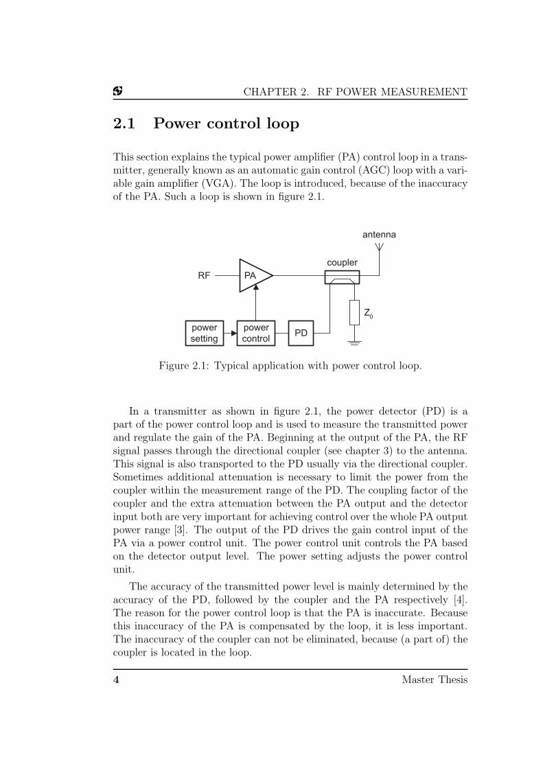
2.1 Power control loop
This section explains the typical power amplifier (PA) control loop in a trans-mitter, generally known as an automatic gain control (AGC) loop with a vari-able gain amplifier (VGA). The loop is introduced, because of the inaccuracyof the PA. Such a loop is shown in figure 2.1.
PA
antenna
coupler
PD
Z0
RF
power
control
power
setting
Figure 2.1: Typical application with power control loop.
In a transmitter as shown in figure 2.1, the power detector (PD) is apart of the power control loop and is used to measure the transmitted powerand regulate the gain of the PA. Beginning at the output of the PA, the RFsignal passes through the directional coupler (see chapter 3) to the antenna.This signal is also transported to the PD usually via the directional coupler.Sometimes additional attenuation is necessary to limit the power from thecoupler within the measurement range of the PD. The coupling factor of thecoupler and the extra attenuation between the PA output and the detectorinput both are very important for achieving control over the whole PA outputpower range [3]. The output of the PD drives the gain control input of thePA via a power control unit. The power control unit controls the PA basedon the detector output level. The power setting adjusts the power controlunit.
The accuracy of the transmitted power level is mainly determined by theaccuracy of the PD, followed by the coupler and the PA respectively [4].The reason for the power control loop is that the PA is inaccurate. Becausethis inaccuracy of the PA is compensated by the loop, it is less important.The inaccuracy of the coupler can not be eliminated, because (a part of) thecoupler is located in the loop.
4 Master Thesis
2.1. POWER CONTROL LOOP
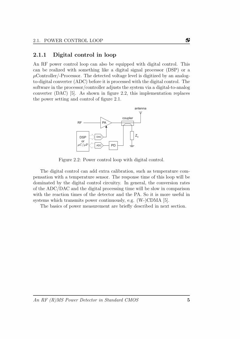
2.1.1 Digital control in loop
An RF power control loop can also be equipped with digital control. Thiscan be realized with something like a digital signal processor (DSP) or aµController/-Processor. The detected voltage level is digitized by an analog-to-digital converter (ADC) before it is processed with the digital control. Thesoftware in the processor/controller adjusts the system via a digital-to-analogconverter (DAC) [5]. As shown in figure 2.2, this implementation replacesthe power setting and control of figure 2.1.
PA
antenna
coupler
PD
Z0
RF
ADC
DACDSP
orµC/µP
Figure 2.2: Power control loop with digital control.
The digital control can add extra calibration, such as temperature com-pensation with a temperature sensor. The response time of this loop will bedominated by the digital control circuitry. In general, the conversion ratesof the ADC/DAC and the digital processing time will be slow in comparisonwith the reaction times of the detector and the PA. So it is more useful insystems which transmits power continuously, e.g. (W-)CDMA [5].
The basics of power measurement are briefly described in next section.
An RF (R)MS Power Detector in Standard CMOS 5

CHAPTER 2. RF POWER MEASUREMENT
2.2 Definition of RMS
Root-mean-square (RMS) is a measure for the magnitude of an AC signal.The RMS value provides the same average power as a DC voltage/current ofthe same level [1]. So it is sometimes indicated with the average. A practicaldefinition is: the RMS value assigned to an AC signal is the amount of DCrequired to consume an equivalent amount of power in the same load [6].The mathematical definition is
VRMS =√
V 2 (2.1)
This means, square the signal, take the average and extract the root. Theaveraging time has to be long enough to allow filtering of the lowest operatingfrequencies.
2.3 Traditional power measurement
Power can be expressed in several ways, e.g. time-dependent, peak or averagepower. Usually the real part of power is more interesting than the imaginarypart. The real power is dissipated or radiated into space and the imaginarypower is stored in capacitors, inductors or in the near fields of an antenna [1].The most commonly used power definition is derived from the measured RMSvoltage VRMS, referred to the (real) impedance level R, as [2]
Pavg =V 2
RMS
R[W ] (2.2)
This is the average power and is also indicated as Peff or PAv.Usually it is sufficient to measure the RMS voltage to calculate the power,
because most communication systems have constant load impedance (usually50 Ω). So many practical power measurement circuits measure only the RMSvoltage, but this is not the right way to measure the radiated power of anantenna, because the impedance of an antenna can change by surroundingobjects, which distort the antenna pattern [7, 8]. This leads to impedancemismatch and causes reflections (see section 3). When this happens, themeasured voltage contains incident and reflected voltages and indicates theradiated power not correctly. Thus for this study, only the incident voltagehas to be provided.
2.3.1 Absolute power levels
Signal levels in communication applications are often given in absolute powerlevels. For power, it has become common practice to use dBm or dBW, which
6 Master Thesis
2.3. TRADITIONAL POWER MEASUREMENT
refers to the power level in dB referenced to 1 mW or 1 W respectively.Likewise, VRMS is given in dBV, which is defined as the voltage level in dB,relative to 1 V. The dBm and dBV levels can be calculated as [9]
Pavg [dBm] = 10 log
(Pavg [W]
1 [mW]
)(2.3)
VRMS [dBV] = 20 log
(VRMS [V]
1 [V]
)(2.4)
When using (2.2) and (2.4) in (2.3)
Pavg [dBm] = 10 log
(V 2
RMS [V2]
R [Ω]· 103
1 [W]
)(2.5)
= 10 log
(10
VRMS [dBV]
20·2 · 1 [W−1]
R [Ω]
)+ 30 [dB] (2.6)
= VRMS [dBV] − 10 log
(R [Ω]
1 [Ω]
)+ 30 [dB] (2.7)
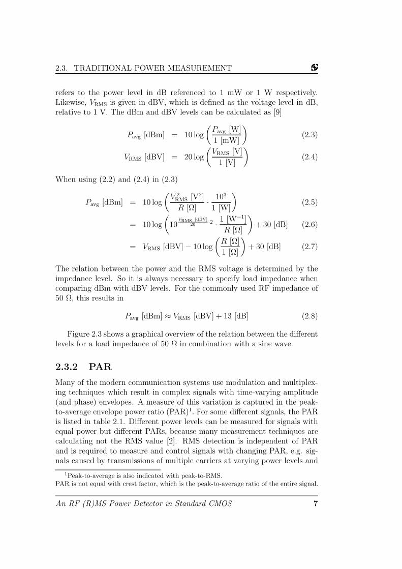
The relation between the power and the RMS voltage is determined by theimpedance level. So it is always necessary to specify load impedance whencomparing dBm with dBV levels. For the commonly used RF impedance of50 Ω, this results in
Pavg [dBm] ≈ VRMS [dBV] + 13 [dB] (2.8)
Figure 2.3 shows a graphical overview of the relation between the differentlevels for a load impedance of 50 Ω in combination with a sine wave.
2.3.2 PAR
Many of the modern communication systems use modulation and multiplex-ing techniques which result in complex signals with time-varying amplitude(and phase) envelopes. A measure of this variation is captured in the peak-to-average envelope power ratio (PAR)1. For some different signals, the PARis listed in table 2.1. Different power levels can be measured for signals withequal power but different PARs, because many measurement techniques arecalculating not the RMS value [2]. RMS detection is independent of PARand is required to measure and control signals with changing PAR, e.g. sig-nals caused by transmissions of multiple carriers at varying power levels and
1Peak-to-average is also indicated with peak-to-RMS.PAR is not equal with crest factor, which is the peak-to-average ratio of the entire signal.
An RF (R)MS Power Detector in Standard CMOS 7

CHAPTER 2. RF POWER MEASUREMENT
by variations in code-domain power in a single code-division multiple ac-cess (CDMA) carrier [10] or something similar. The high-frequency CDMAcarrier has very complex (noise-like) modulation envelopes with high PAR,produced by complicated transmission algorithms.
Signal PAR [dB]
sine wave 0square wave/DC 0gaussian noisea 9–12ADSL 15GSM 0EDGE 3.2W-CDMAb (16 channels) 10802.11a (52 carriers) 10
Table 2.1: PAR for different signals [2, 9, 11, 12, 13].
aNoise has not a peak level, because it is random. Thus the ratio is dependent on theallowable error. The higher the ratio, the less the error. The values in this table give anerror of 0.5–1.5% [11].
bGenerally, it is in the range 5 − 10 dB for handhelds and can even be higher for basestations
From all signals in table 2.1, the W-CDMA signal (2 < f < 3 GHz) isthe most relevant for this study. Nowadays, these signals are used in moderncellular phones e.g. UMTS in 3G cellular phones. When such a cellularphone uses the GSM standard (f < 1 GHz), the GSM signals are importanttoo. Actually, (almost) all RF signals with a high PAR are related to thisstudy.
It is difficult to perform accurate measurements over a wide measurementrange at RF frequencies of several GHz. The need for such measurements isincreasing, because modern communications systems, as CDMA, have a verywide bandwidth and high operating frequencies.
8 Master Thesis

2.3. TRADITIONAL POWER MEASUREMENT
+10
+1
0.1
0.01
10
1
0.1
0.01
0.001- 60
- 50
- 40
- 30
- 20
- 10
0
+10
+20
- 50
- 40
- 30
- 20
- 10
0
+10
+20
+30
0.00001
0.0001
0.001
0.01
0.1
1
10
100
1000
Figure 2.3: The relation between the different levels for a load impedance of50 Ω in combination with a sine wave [9].
An RF (R)MS Power Detector in Standard CMOS 9

CHAPTER 2. RF POWER MEASUREMENT
10 Master Thesis

Chapter 3
Directional coupler
This chapter discusses the directional coupler that is frequently used inpower-measuring systems e.g. as in figure 2.1 in the previous chapter. Inthis project, the coupler will be used in relation with the PD, but it is outof this project to develop the coupler.
A transmission line coupler can be formed by placing two lines in paralleland close together, so that energy propagating on one is coupled to the other.The energy on both lines travels in opposite direction. The coupled powertravels backward and that is why the coupler is called a backward wavecoupler [1].
Consider the coupler in figure 3.1. The input power PIN enters the cou-pler at port 1. Ideally, the desired coupled power PC exits at port 2 and theremaining (being left) power PL exits at port 4. However, due to imperfec-tions, some power PD exits at port 3 (decoupled port) and some power PR
reflects at the input port.
The parameters of couplers are (in dB)[1]:
Coupling = 10 log
(PIN
PC
)
Directivity = 10 log
(PC
PD
)
Isolation = 10 log
(PIN
PD
)
= Coupling + Directivity
Return loss = 10 log
(PIN
PR
)
Insertion loss = 10 log
(PIN
PL
)
11

CHAPTER 3. DIRECTIONAL COUPLER
vIN
PL
PD
PIN
PC
PR
Z0
Z0
Z0
Z0
1 4
2 3
Figure 3.1: The backward wave coupler [1].
The directivity is infinite when no power exits at port 3. The magnitude ofthe output voltage at port 2 relative to the input voltage at port 1 is thecoupling coefficient.
When choosing the right dimensions for the coupler, the entering powerat port 1 exits at port 2 and 4 with no power exiting at port 3 for anyfrequency and for any coupling coefficient. Furthermore, there is exactlya 90 phase difference at all frequencies between the signals from ports 2and 4. Thereby the loads at all ports have to be the same. This idealperformance degrades by the mismatch and reflections of practical couplers.The reflections occur by the transitions from the ends of the coupled lines inorder to attach connectors at the ports.
It is necessary to use a directional coupler as a part of a power detectionloop. Of course, there are other possibilities, but they do not provide anydirectivity. The higher the coupler directivity, the more independent is thedetected voltage from reflections. These reflections are generated by a mis-matched antenna. Then the PD measures the superposition of the forward-oriented and the unwanted backward-oriented (reflected) power. When thesereflections are negligible or constant (PD can be calibrated), the accuracy ofthe PD is high.
Especially for systems with wideband antennas, it is impossible to assurelow reflections across the whole band and under all practical conditions of
12 Master Thesis

usage. Even when the antenna itself has an acceptable return loss, it couldsometimes be operated in close vicinity of surrounding objects. In practice,the user of a mobile phone covers the antenna by hand and head, whichwill distort the antenna pattern and seriously degrade the matching. So it isobvious that only the forward-oriented power would be detected, independentfrom the antenna matching. This is also the main reason for using directionalcouplers in many WLAN cards.
When achieving a good directivity for the individual coupler in a system,a good overall system directivity is not guaranteed. So the system directivityis not only limited by the coupler parameters [7].
The coupled output power is smaller than the input power, caused bythe coupling factor of the coupler. Directional couplers are characterized bytheir coupling factor, which is typically in the range of 10 to 30 dB, i.e. theoutput signal of the coupler is 10 to 30 dB smaller than the output of thePA. The typical value is 20 dB. Because in this study the coupled outputhas to deliver some power to the detector, the coupling process takes somepower from the main output (port 4). This manifests itself as insertion loss.Lower coupling factors result in higher insertion loss.
An RF (R)MS Power Detector in Standard CMOS 13

CHAPTER 3. DIRECTIONAL COUPLER
14 Master Thesis

Chapter 4
Power detectors
The first RF transmissions were immediately followed by the need for RFpower measurement. There are different techniques to measure power. Someof them are discussed in this chapter.
The precision of the measurement may be critical, especially when the PAworks at, or close to, full power. For example, consider a PA which transmitsan average power of 30 dBm (1 W)1. The transmitted power from the PA isregulated by a PD. If this PD has an unpredictable error over temperature of+/−3 dB, it is possible that the PA can sometimes transmit 33 dBm (2 W).This means a doubled transmitting power. This is unacceptable, because itrequires additional thermal dimensioning of the unit and adds excessive costfor a safely transmit without overheating. However, the tolerance of outputpower at lower power levels is important for being within the limits of thestandards.
This study deals with many of the issues associated with measuring RFpower levels. Various power measurement techniques will be discussed in thischapter. Issues such as response time (measurement agility), dynamic range,power consumption, resolution, varying crest factor (waveform dependence),temperature stability, size and cost will also be examined. The developmentof many radio communication systems leads to several different designs fordedicated power detector integrated circuits. The search for low cost, accu-rate, small RF detectors has lead to innovative IC solutions focused on thecritical parameters.
The complex signals of nowadays communication systems leads to inte-grated circuits based on logarithmic amplifiers and RMS detectors. Thesetechniques offer versatile operation for various types of signals.
First the important parameters are listed.
1See subsection 2.3.1 for the relation between both units.
15

CHAPTER 4. POWER DETECTORS
4.1 Parameters
The most important parameters with respect to power detectors are summedand described in this section [14].
Operating frequency
The RF signal frequency is one of the most important parameters of a de-tector. The detector has to provide a constant response over the desiredfrequency range. To achieve this, two internal parameters are critical: sensi-tivity (or gain) variation versus frequency and the input impedance matching.
Sensitivity vs. linearity
The sensitivity of the detector is the ability of the system to return usableinformation from a very low input signal. The minimum input signal levelhas to be larger than the minimum required output signal level of the detec-tor. The sensitivity is not always higher (better) by simply increasing gain,because the detector can be saturated by gain when the maximum inputsignal level is amplified. Then it is better to amplify nonlinear by decreasinggain with increasing input level. For this reason, detectors are classified inlinear and nonlinear.
Environmental variations
A detector has to be independent of the environmental variations. The sys-tem implementation determines the requirements on the power supply rejec-tion and temperature variation. The power supply rejection performance isusually much higher for integrated detectors than for discrete solutions. Gen-erally, the power supply is regulated, which provide more protection againstpower variations. The temperature variation can not minimized easily, be-cause it is difficult to implement an accurate temperature measurement. Sothe detector itself determines the temperature variation.
16 Master Thesis

4.2. PEAK DETECTION
4.2 Peak detection
An easy way to measure power is peak detection, which extracts the ampli-tude of the input signal. Figure 4.1 shows the typical application with peakdetection.
PA
antenna
coupler
PD
Z0
RF
power
control
power
setting
v(v)
Figure 4.1: Typical application with peak detection.
The basic function of peak detection is shown in figure 4.2. The inputsignal is rectified by a half or a full rectifier and after that, it is averaged bya low-pass filter (LPF), which provides the output signal.
VOUT
RFIN
Figure 4.2: Block diagram of the basic function of peak detection.
The output voltage of a peak detector is proportional to the amplitude ofthe input voltage. The information in an amplitude modulated input signalis directly accessible in the detected voltage. However, this output voltageof the detector varies with PAR, because it is not a measure of true RMSpower. So for signals with high PAR, it provides not the correct value of thetransmitted power.
Some different ways for peak detection are described in this section.
4.2.1 Diodes
For power detection, (Schottky) diodes are commonly used. The reasonsfor its popularity are simple circuits and high frequency ability. The diodesare configured as peak detectors and rectify the input signal with one [2],two [2] or four [7] diodes. The simple implementations with one and twodiodes are illustrated in figure 4.3(a) and 4.3(b) respectively. The added RCnetwork provides the averaging. These detectors can have wide detectionbandwidths and can respond to high frequencies. The diode detector has
An RF (R)MS Power Detector in Standard CMOS 17

CHAPTER 4. POWER DETECTORS
very high resolution at high input levels. Diodes also vary on temperature,but this can be minimized with additional components, e.g. the second diode.The transfer function, the relation between output voltage and input signallevel, is not completely linear. For signal detection with diodes in the GHzregion, the cost of power dissipation, matching design and large chip areamay become critical [15].
vOUT
RF
R1
C1
R2
D1
(a) One diode implementation.
vOUT
RF
R1
C1
R2
D1 R
3
D2
(b) The second diode compensates tempera-ture dependency.
Figure 4.3: Simple diode detectors as half wave rectifiers with RC networks.
Diodes versus MOSFETs
In a comparable circuit with a metal-oxide-semiconductor field-effect tran-sistor (MOSFET or MOST) instead of a diode, the sensitivity, temperatureindependency and noise level can be improved [16].
18 Master Thesis

4.2. PEAK DETECTION
4.2.2 Bipolar transistors
An RF power detector can be realized with bipolar transistors. A mono-lithic low power RF peak detector using bipolar transistors was developedby Meyer [17] as shown in figure 4.4(a).
vOUT
RF
C1
Q1
Q2
R1
R2
I1
I2
C2
(a) Without voltage divider.
RF
C1
Q1
Q2
R1
R2
I1
I2
C2
C3
R4
R3
vOUT
(b) Voltage divider included.
Figure 4.4: Bipolar transistors implementations.
The input voltage is rectified by bipolar transistor Q1. When the ACinput signal is zero, Q2 balances the DC output voltage to zero by offering aDC offset voltage. Both capacitors filter out the AC signal and power supplynoise. The DC biases of both transistors should be equal to cancel any DCoffset error. This circuit has two detection regions as shown in figure 4.5.The square law detection for small signals can be approached by [15]
vOUT ≈ v2RF
4VT(4.1)
and the linear detection for large signals can be approached by [15]
vOUT ≈ vRF − VT ln
√2πvRF
VT(4.2)
with VT ≈ 25 mV. However, there is a crossover region between them inwhich it is hard to detect the input signal with simple models [15].
This circuit has the advantages of simplicity, low power, wide bandwidth,temperature stability and small chip size, but it is not suited for a largedynamic range2. The dynamic range can be improved with adding a voltagedivider as shown in figure 4.4(b) [15]. This voltage divider minimizes thecrossover region by applying a divided input signal to the base of Q2.
2See subsection 5.1.2 for an explanation of dynamic range
An RF (R)MS Power Detector in Standard CMOS 19
CHAPTER 4. POWER DETECTORS
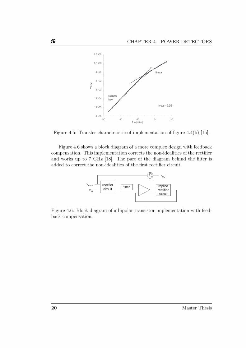
Figure 4.5: Transfer characteristic of implementation of figure 4.4(b) [15].
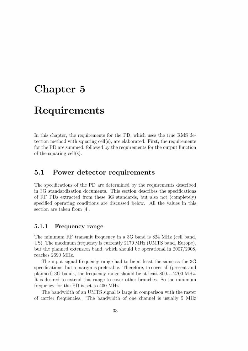
Figure 4.6 shows a block diagram of a more complex design with feedbackcompensation. This implementation corrects the non-idealities of the rectifierand works up to 7 GHz [18]. The part of the diagram behind the filter isadded to correct the non-idealities of the first rectifier circuit.
rectifier
circuitvIN
vOUT
vBIAS
filter replica
rectifier
circuit
PFigure 4.6: Block diagram of a bipolar transistor implementation with feed-back compensation.
20 Master Thesis

4.3. LOGARITHMIC DETECTION
4.3 Logarithmic detection
A more advanced type of a peak detector is based on a logarithmic amplifieror log-amp. For integrated power measurement, the log-amp is often used.A classic example is using the log-amp as a PD in a power control loop. Thelog-amp calculates the log of the envelope of an input signal.
y = log(x) (∀x > 0) (4.3)
A simplified architecture of a log-amp is illustrated in figure 4.7. Theoutput is a piece-wise linear approximation of the log of the input. Thecore of a log-amp consists of a cascade of limiting amplifiers with preciselinear gains. The outputs of the amplifiers are limited for large enough inputsignals. The shown architecture consist of five amplifiers, each with a gainof 20 dB, who are clipping (limiting) at 1 V peak. The outputs of theseamplifiers are detected by full rectifiers, summed together and averaged byan LPF successively. The logarithmic function between input and outputsignal level is due to the successive compression of the cascaded gain stages.
∑
Figure 4.7: Log-amp architecture [9].
The ability of a log-amp is to convert a signal, which varies over a largedynamic range3, into a signal with a much smaller range [9]. The obviousadvantage of a log-amp is that it has a very high dynamic range and a verylinear transfer characteristic. The stability of the log-amp is excellent. Log-amps can have wide detection bandwidths over a very broad frequency range.It is even possible to realize it completely in CMOS [19]. A Log-amp also
3See subsection 5.1.2 for an explanation of dynamic range
An RF (R)MS Power Detector in Standard CMOS 21

CHAPTER 4. POWER DETECTORS
offers excellent accuracy [2], but it has the same disadvantage as the diodedetection; the output voltage of a log-amp varies with PAR, because it is notRMS responding.
22 Master Thesis

4.4. TRUE RMS DETECTION
4.4 True RMS detection
The previous discussed detectors are sensitive to PAR. This dependence onPAR is eliminated by an RMS responding detector. This detector convertsan RMS value of an arbitrary signal into a quasi-DC signal that representsthe true power level of the arbitrary signal. Such detectors are also calledRMS-to-DC converters. Figure 4.8 shows the typical application with RMSdetection.
PA
antenna
coupler
PD
Z0
RF
power
control
power
setting
v(vRMS
)
Figure 4.8: Typical application with RMS detection.
Some different ways of RMS detection are described in this section.
4.4.1 Thermal detection
A fundamental technique for measuring RMS power is thermal detection.This is the simplest RMS detection in theory, but in practice it is difficultand expensive to implement. Figure 4.9 shows the typical application withthermal detection.
PA
antenna
coupler
PD
Z0
RF
power
control
power
setting
v(T)
Figure 4.9: Typical application with thermal detection.
An implementation of a PD with thermal detection is shown in figure 4.10.The input signal and a reference voltage both heat a resistor and also theadjacent thermocouples separately [2]. The output voltages of the thermo-couples are proportional to the temperature. The difference between these
An RF (R)MS Power Detector in Standard CMOS 23

CHAPTER 4. POWER DETECTORS
output voltages is a scaled measure of the input power relative to the refer-ence power.
Figure 4.10: Implementation of a PD with thermal detection [2].
Thermistors in a bridge configuration can achieve a similar result [20].The circuits with thermocouples or thermistors both can be very accurateand provide RMS detection, because the temperature difference is propor-tional to the power. Important for the accuracy are matching and thermalisolation to minimize dependency between the thermistors or thermocouples.Disadvantages are slow thermal time-constants which determine the responsetime and the system is not easy to integrate [2]. Moreover, it is difficult touse for low power applications [18].
4.4.2 Log-antilog detection
For measuring RMS power, it is also possible to use the exponential relationof a junction, because the natural logarithmic (the inverse of exponential)relation can implement some other functions, for example
ln(xn) = n ln(x) (4.4)
The RMS value can be determined with this relation. The square and square-root functions can easily be implemented as
ln(x2) = 2 ln(x) (4.5)
ln(x0.5) = 0.5 ln(x) (4.6)
The typical log-antilog RMS detection is shown in figure 4.11. The as-sumption is that the input current is continuously positive (iIN > 0).
24 Master Thesis

4.4. TRUE RMS DETECTION
v1
v2
v3
v4
v(i) i(v) iOUT
iIN
Figure 4.11: Block diagram of log-antilog detection.
First a forward-biased semiconductor junction conducts the input currentand produces a voltage. This is proportional to the natural logarithm of theinput current.
v1 = ln(iIN) (4.7)
After that, this voltage is doubled by a multiplier circuit and provides thesquare function of the input current (see equation (4.5)).
v2 = 2 ln(iIN)
= ln(i2IN) (4.8)
Afterwards the voltage is averaged by an LPF.
v3 = ln(i2IN) (4.9)
≈ ln(i2IN) for iIN > 0 (4.10)
Subsequently, a divider circuit halves the averaged voltage. This providesthe square-root function of the averaged, squared input current (see equa-tion (4.6)).
v4 =1
2ln(i2IN)
= ln
(√i2IN
)(4.11)
Finally, another forward-biased semiconductor junction produces an outputcurrent of this halved voltage. The output current is proportional to theRMS value of the input current.
iOUT = eln
qi2IN
=
√i2IN (4.12)
Log-antilog RMS detectors are very low power, but they have several dis-advantages [21]. Firstly, the input of any logarithmic computation has tobe positive. So when the input becomes negative, log-antilog RMS detectorsrequire an absolute value circuit before the detector. Such an absolute value
An RF (R)MS Power Detector in Standard CMOS 25

CHAPTER 4. POWER DETECTORS
circuit is difficult to implement, because it typically contributes offset, po-larity gain mismatch and frequency-/amplitude-dependent errors. Secondly,the dynamic range4 is limited, because the detector is sensitive to mismatchand noise. The amplitudes of the signals between the forward-biased semi-conductor junctions are much smaller than conventional signal levels. Thisresults in enhancement of errors caused by component tolerances, thermaldrift, mechanical stress and other factors, because these errors exert moreinfluence on small signals.
4.4.3 Squaring cell detection
Another concept for RMS detectors is implementing the RMS function insilicon with the usage of squaring cells. Figure 4.12 demonstrates the blockdiagram of this kind of RMS detector. The figure shows a MS detector, butthe root function can be realized by a feedback loop. This feedback loop isexplained later on.
x2 +
-
sSQR
sIN
sREF
sOUT
VGA
sCTRL
P ∫
Figure 4.12: Block diagram of the MS responding detector approach withsquaring cell detection.
The input signal sIN is amplified by the VGA, squared by a squaring celland averaged. The control signal sCTRL is used to control the gain of theVGA. For RF applications, the averaging circuit has to provide two types ofaveraging: RF ripple filtering of the carrier signal and long-term averaging ofthe modulation envelope. In literature, this is realized by the LPF and theintegrator respectively as shown in figure 4.12. Between these two blocks, areference signal sREF is subtracted. In this section, this implementation ofaveraging should be assumed, because the averaging is less important and isdiscussed later on.
For extracting the true RMS value of a CDMA signal, the filtering timeconstant has to be quite long compared to the carrier period, because of itsnoise-like modulation envelope. Besides, a CDMA signal has high PAR anddeviates not often far from the baseline, but when it happens, the peaks arehigh. So an RMS detector for such signals has to be able to provide both
4See subsection 5.1.2 for an explanation of dynamic range
26 Master Thesis

4.4. TRUE RMS DETECTION
a filter with a long time constant for the modulation envelope and accurateresponse to the power contained in the high-frequency waveform peaks [22].
In literature, the LPF (for the RF ripple filtering of the carrier signal) isrealized with a relatively short time constant of typically about some nanosec-onds. The integrator (for the long-term averaging of the modulation enve-lope) has a relatively long time constant and should be on a time scale ofmilliseconds or even longer [23].
Sometimes it is possible to combine both types of averaging in a singlecomponent [23]. A capacitor can combine both functions. The integratedfunction is realized as
uC(t) = UC(t0) +1
C
∫ t+t0
t0
iC(t)dt (4.13)
and in combination with the output impedance of the squaring cells, it formsthe LPF.
Measurement vs. controller mode
The RMS detector can be configured for operation in measurement or con-troller mode as shown in figure 4.135. For all implementations, the loop hasto have a negative feedback.
squaring
cell
detector
sIN
sREF
sCTRL
sOUT
(a) Operation in measure-ment mode.
PA
antenna coupler
squaring
cell
detector
Z0
RF
sIN
sREF
sOUT
sCTRL
sSETPOINT
(b) Operation in controller mode.
Figure 4.13: Simplified schematics how the RMS detector can be configuredfor operation in measurement or controller mode.
In measurement mode, the output signal sOUT is connected to the controlsignal sCTRL. In controller mode, the output signal is used to control thegain of the PA. The PA provides the input signal sIN to this detector via thedirectional coupler. So there is a feedback loop realized. Then the control
5The signals in this figure can be a current or a voltage even in fully differential mode.
An RF (R)MS Power Detector in Standard CMOS 27

CHAPTER 4. POWER DETECTORS
signal is applied to a setpoint signal sSETPOINT and determines together withthe reference signal sREF, the power from the PA to balance the loop. Insome detectors a VGA is not included and then the control signal is notpresent. This means in measurement mode that the feedback loop is realizedby connecting the output signal to the reference signal.
All following examples in this section are explained in controller mode,since this study is meant for that application.
Difference-of-squares
The RMS function of these converters is usually realized by implementingthe ‘difference-of-squares’ function by two identical squaring cells. Such RMScalculations provide wide detection bandwidths, as also stable scaling fac-tors [2]. Figure 4.14 demonstrates a block diagram of such an RMS detector.
x2
x2
CAV
+
-iREF
iSQR
sIN
sREF
sOUT
iERR
VGA
sCTRL
PFigure 4.14: Block diagram of an example of an RMS responding detectorapproach by implementing the difference-of-squares function.
Figure 4.14 shows an example of an RMS responding detector by imple-menting the difference-of-squares function. The first (upper) squaring cellis also called the high frequency (HF) squaring cell and the second (lower)identical squaring cell is also called the DC squaring cell. For operation incontroller mode, the feedback loop is closed around the HF squaring cell. Inmeasurement mode, the loop is closed around the DC squaring cell insteadof the HF squaring cell. The loop is balanced when the average value of theerror current iERR is zero. Since the feedback loop is always closed around asquaring cell, an implicit square-root function is implemented [22].
In figure 4.14, the RF input signal is applied to the HF squaring cellvia a VGA. This VGA amplifies the input signal with a gain established bythe control signal and determines the scaling factor. The reference currentfrom the DC squaring cell is subtracted from the output current of the HFsquaring cell, which is a fluctuating current with a positive mean value. Thereference signal of the RMS detector is applied to the DC squaring cell and
28 Master Thesis

4.4. TRUE RMS DETECTION
can be a voltage or a current. The error current
iERR = iSQR − iREF (4.14)
is averaged by the capacitor. For isolating the error current from the outputsignal, a buffer is used. The squared signal delivered from the HF squaringcell is forced to equal the reference signal delivered from the DC squaringcell.
iSQR = iREF
(sIN · C1)2 = s2
REF√(sIN · C1)
2 =
√s2REF
When the feedback loop is closed and balanced, the output signal is equal tothe reference signal. For the reason that the output signal is a DC signal
√(sIN)2 · |C1| =
√s2OUT√
(sIN)2 · |C1| = sOUT (4.15)
So with a closed loop, the output is related to the RMS value of the inputsignal.
The detected output signal is independent of the PAR at the input sig-nal, as long as the squaring cells can handle the input signal completely [2].Several benefits arise when using two identical squaring cells. For example,the tracking in the responses of the cells remains very close over tempera-ture [24]. Accurate RMS measurement at high frequencies can be realized byusing carefully balanced squaring cells and a well-balanced error amplifier.In case of using a reference current, the DC squaring cell can be skipped, butthe advantages of using two identical squaring cells are perished.
Additionally, the summing node can also be carried out with voltages,but the advantage of currents is the easy way to realize the summing nodewith a simple (wire) connection without any additional components. Thisminimal structure is very effective at high frequencies [22].
Another observation is that the HF squaring cell is the only part of thecircuit, which has to operate at the input signal frequencies, because itsoutput is immediately low-pass filtered by the capacitor. So the remainderof the circuit can operate at lower frequencies.
Some available RMS detectors based on figure 4.14 are listed in appen-dix A. One of these existent ICs, AD8362, is discussed in appendix A.1.
An RF (R)MS Power Detector in Standard CMOS 29

CHAPTER 4. POWER DETECTORS
Dynamic range extension
There are also some other improvements possible in the system of figure 4.14.The same baseband modulation signal that is used to modulate the carriersignal is now applied as the reference signal to the second squaring cell, ratherthan a fixed DC reference signal. In this way with two equal squaring cells, allthe square law conformance errors of the squaring cells are cancelled. Anotherimprovement is moving the VGA to the reference signal path. The advantageis that the VGA need only operate at the frequency of the baseband signalrather than the carrier signal. Using a VGA in either the input signal path orthe reference signal path enhances the system accuracy over a wide dynamicrange6. See [25] for more details about a suitable VGA.
For signals with wide bandwidth and high operating frequencies, the RMSdetector has to provide a very wide measurement range. The dynamic rangecan be improved (extremely) when using a series of gain stages and vari-able weighting coefficients as shown in figure 4.15 [26]. The schematic offigure 4.15 should replace the VGA and the squaring cell of figure 4.12. The
vIN
iOUT
x2
G
vCTRL
x2
G
x2
G
x2
Interpolator
1 2 3 Nαααα
Figure 4.15: Squaring cell implemented as a series of gain stages and variableweighting coefficients.
series of gain stages generates a single series of amplified signals, which areindividually squared and weighted and finally summed to provide the outputsignal. The output signal has to be averaged and utilized in the same man-ner as a single stage squaring cell. Each squaring stage includes a squaringcell with a fixed scale factor and also includes the weighting stage, whichmultiplied the squared signal with a weighting signal αn. The interpolatorgenerates the weighting signals in response to the control signal vCTRL, whichfunctions identical as the control signal of figure 4.12. Usually, the weightingsignals are a series of continuous overlapping Gaussian-shaped current pulses.During operation, most of the weighting signals are nearly zero and disables
6See subsection 5.1.2 for an explanation of dynamic range
30 Master Thesis

4.5. CONCLUSION
most of the squaring stages.The system of figure 4.15 can be implemented with any number of gain
stages.
IOUT = V 2IN
N∑
n=1
αnGn−1 (4.16)
Some of the lower numbered gain stages can be attenuators instead of am-plifiers. So the system can provide wide dynamic range at high frequencies,e.g. ten (attenuating and amplifying) gain (each 10 dB) and squaring stagesprovide an overall dynamic range of 100 dB.
4.5 Conclusion
This study is meant for a PD, which is suitable for RF signals with high PAR,especially CDMA signals. For this reason, peak and logarithmic detectionare not suited, because their outputs are dependent on PAR. On the otherhand, true RMS detection is (much more) independent on PAR.
Thermal detection is one possible implementation of RMS detection, butin practice it is difficult and expensive to implement. Moreover, it is requiredto implement the PD in standard CMOS. The second possible implemen-tation is log-antilog detection. The major disadvantage of this manner ofdetection is the limited dynamic range, because of the sensitivity to noiseand mismatch. The reason for this are the (very) small amplitudes of thesignals between the forward-biased semiconductor junctions. The third wayof RMS detection is the use of squaring cells. This implementation is easyto implement; it has been already realized using bipolar transistors. Some ofthese bipolar squaring cells are discussed in appendix E. This way of RMSdetection is suited for this study. However in this study, the PD should beimplemented in a standard CMOS process.
An RF (R)MS Power Detector in Standard CMOS 31

CHAPTER 4. POWER DETECTORS
32 Master Thesis
Chapter 5
Requirements
In this chapter, the requirements for the PD, which uses the true RMS de-tection method with squaring cell(s), are elaborated. First, the requirementsfor the PD are summed, followed by the requirements for the output functionof the squaring cell(s).
5.1 Power detector requirements
The specifications of the PD are determined by the requirements describedin 3G standardization documents. This section describes the specificationsof RF PDs extracted from these 3G standards, but also not (completely)specified operating conditions are discussed below. All the values in thissection are taken from [4].
5.1.1 Frequency range
The minimum RF transmit frequency in a 3G band is 824 MHz (cell band,US). The maximum frequency is currently 2170 MHz (UMTS band, Europe),but the planned extension band, which should be operational in 2007/2008,reaches 2690 MHz.
The input signal frequency range had to be at least the same as the 3Gspecifications, but a margin is preferable. Therefore, to cover all (present andplanned) 3G bands, the frequency range should be at least 800. . . 2700 MHz.It is desired to extend this range to cover other branches. So the minimumfrequency for the PD is set to 400 MHz.
The bandwidth of an UMTS signal is large in comparison with the rasterof carrier frequencies. The bandwidth of one channel is usually 5 MHz
33

CHAPTER 5. REQUIREMENTS
(1.6 MHz for time division multiplexing at half-rate) and the carrier fre-quencies are 200 kHz from each other.
5.1.2 Absolute power accuracy
The absolute output power accuracy defines the acceptable tolerance and isonly specified for the maximum transmit power level. The other power levelsare provided by a relative, and not by a absolute, tolerance.
The absolute accuracy for the maximum transmit power level is ±2 dB or−3. . . +1 dB. For the other power levels, based on 7 to 10 consecutive powersteps, indicative values are given in table 5.1. Because the accuracy of the
Output power [dBm] Maximum error [dB]
−50. . . 0 ±90. . . +24 ±4
+24. . . +28 ±2
Table 5.1: Indicative absolute output power specifications for a 3G transmit-ter.
PD is very important, the maximum error should be a half of the values oftable 5.1. So, the target requirement is to keep the power measurement errorsmaller than 1 dB for all operating conditions as the temperature range, thesupply voltage range and the dynamic range.
Law conformance
The difference between the ideal (predefined) and measured transfer charac-teristics results in a ripple error and is named the law (or log) conformance(error). A typical transfer characteristic and log conformance error for alog-amp at 1.9 GHz are shown in figure 5.1. The ideal line is the best fitted(linear) line to the measured transfer characteristic and is defined by theslope and the intercept as
vOUT,ideal = slope(PIN − intercept
)(5.1)
The intercept is the input signal level of the ideal line when the output voltageis zero, i.e. when the ideal line crosses the horizontal axis. This ideal responseis a model for the detector transfer. The better this model, the better theaccuracy. The values for intercept and slope are usually determined at thegenerally operating conditions: room temperature with a selected test signal.Then the best model is obtained. The remaining errors are reputed to be
34 Master Thesis

5.1. POWER DETECTOR REQUIREMENTS
Figure 5.1: A typical transfer characteristic and log conformance error for alog-amp at 1.9 GHz [27].
temperature variation and possibly variation for different input signals, butan RMS detector is (almost) independent on different input signals.
For example, if the input signal in figure 5.1 is −50 dBm, the outputvoltage follows from equation (5.1)
vOUT,ideal = 18 [mV/dB](− 50 [dBm] −−100 [dBm]
)
= 0.9 V
With using (5.1), the error is defined as
ε [dB] =vOUT,meas − vOUT,ideal
slope(5.2)
=vOUT,meas − slope
(PIN − intercept
)
slope(5.3)
=vOUT,meas
slope− PIN + intercept (5.4)
The error curve represents the stability and the accuracy of the detector.The stability of the detector manifests itself in the variations in the lawconformance, slope and intercept [2].
Dynamic range
The dynamic range (DR) of a PD is defined as the input power range of thelaw-conformance for which it meets a predefined accuracy over all operating
An RF (R)MS Power Detector in Standard CMOS 35
CHAPTER 5. REQUIREMENTS
conditions. The law conformance (maximum allowed error) has a typicalvalue of better than ±1 dB [2]. Nowadays, also smaller values are used1.
The middle section of the error curve (with small error variation) answersthe maximum allowed error and is called the dynamic (or detection) range(DR). The detector is used in this range. At the low end of the error curve, theDR is limited by signal offsets and mostly temperature variations. At the highend, the large error is caused by output clipping, because the output voltageapproaches the maximum signal swing that the detector can handle [24, 30].
For example in figure 5.1, the input range is from −70 dBm to −8 dBmfor log conformance within ±0.5 dB.
Because the detector should only meet the accuracy requirements at hightransmit power levels, the 80 dB output power DR as mentioned in table 5.1is not necessary. In order to satisfy all requirements (for absolute and relativepower accuracy), the controllable range of output power has to be around30 dB. This is usually sufficient, but a larger DR gives more flexibility forselection of other system components, e.g. the coupler.
Input power range
The absolute input power range for the detector is determined by the max-imum PA output power and the coupling factor of the coupler. A suitablerange for the input power level is around −5. . . +15 dBm.
The input resistance of the detector should be 50 Ω, because the direc-tional coupler had to be connected to a characteristic load (see chapter 3).However, this is not important for this study, because an input amplifier isplaced between the coupler and the detector. This input amplifier convertsthe output signal of the coupler to a signal, which the detector needs (usuallya differential voltage or differential current).
5.1.3 Relative power accuracy
The relative (or differential) power accuracy specifies the response of thedetector to a predefined power step at the input for all operating conditions.During the power step, all other operating conditions are assumed to beunchanged. For power control, the requirements for a single 1 dB power stepand for ten consecutive 1 dB power steps (10 dB) are most important.
The accuracies of PDs for 1, 2 and 3 dB steps are usually highly correlated.So, it is sufficient to concentrate at the most strict requirement, which isusually an 1 dB step. The detector accuracy for a (single) 1 dB power step
1±0.5 dB [28] and even ±0.25 dB [24, 29].
36 Master Thesis

5.1. POWER DETECTOR REQUIREMENTS
is ±0.25 dB, i.e. when the input power is 1 dB increased, then the outputpower should indicate a power step between 0.75 and 1.25 dB.
The allowed tolerance of the PD for a 10 dB power step is ±1 dB.
5.1.4 Output power transient response
The transmitted output power must comply with the requirements for thetime masks, which are specified by the 3G standard. This time masks makesdemands on rise time.
The requirements on the transient response are less rigorous, because thetime for a new power update is much longer then the rise time. The reasonfor this is the much slower variation of other environmental conditions, whichcan result in errors e.g. a change of the operating temperature. For savingpower, the PD is turned off until a new power update is required. Thisshutdown function should be provided by a logic interface, but can be leavedout of consideration for this study.
The rise, fall and turn-on times had to support all time slots. A rise orfall time of 5 . . . 10 µs is usually sufficient. The turn-on time is allowed to besomething longer up to 15 . . . 20 µs.
5.1.5 Operating temperature
The standard operating temperature range for cellular phones and base sta-tions is between −40 C and +85 C. It is usually less important to meet thespecifications at the bottom end of the temperature range. More importantis the top end, because the device is generally slightly higher than the back-ground temperature (self-heating). When the detector is placed close to e.g.the PA, it is recommended to extend the range up to a higher temperature,but this is not taken into account.
When the ideal transfer is optimized (for room temperature), the remain-ing error is mainly due to temperature variation.
5.1.6 Power supply
The supply voltage of the detector is generally related to the supply voltage ofthe PA. Usually, a regulator is used between these supply voltages to reducepotential cross talk. PA supply voltages for 3G applications are typicallyround 3.6 V. The target supply voltage is 2.7. . . 3.3 V. These voltages arespecified for the final product.
This study is carried out with simulations and not with real measure-ments. Thus for simulations, the supply voltage is set to 1.8 V, because
An RF (R)MS Power Detector in Standard CMOS 37

CHAPTER 5. REQUIREMENTS
the circuit design is implemented in National’s 0.18µm CMOS9 technologyprocess.
The supply current during active operation may be up to 10 mA.
5.1.7 Summary of requirements
Table 5.2 summarizes the target requirements for the detector followed fromthe 3G standardization and other operating conditions are added to completethe specifications.
Table 5.2: Summary of specifications for the PD.Parameter Min Typ Max Unit
Operating frequency f 400 2700 [MHz]Absolute power accuracy ±1 [dB]
Dynamic range DR 30 [dB]Input power PIN −5 15 [dBm]
Relative power accuracyFor 1 dB power step ±0.25 [dB]For 10 dB power step ±1 [dB]
Rise time tR 5 10 [µs]Fall time tF 5 10 [µs]Turn-on time tON 15 20 [µs]Operating temperature T −40 85 [ C]Supply voltagea VDD 1.6 1.8 2 [V]Supply current IDD 10 [mA]
aThis is the internal voltage used for simulations. The final product needs 2.7. . . 3.3 V(external)
38 Master Thesis
5.2. SQUARING CELL REQUIREMENTS
5.2 Squaring cell requirements
The output function of the squaring cell should be at least square the inputsignal.
sSQR = s2IN (5.5)
Afterwards, this output is averaged. This means that all terms are allowed
sSQR = s2IN + f(sIN) + g(sIN) (5.6)
when
f(sIN) = 0 (5.7)
g(sIN) < εmax · s2IN (5.8)
The average value of a function x(t) over the interval [a, b] is defined as
x(t) =1
b − a
∫ b
a
x(t)dt (5.9)
5.2.1 Exact MS
When the input signals are defined as
x1(t) = X sin(ωt)
x2(t) = X cos(ωt)
The average values of these input signals are
x1(t) =1
T
∫ T
0
X sin(ωt)dt
x2(t) =1
T
∫ T
0
X cos(ωt)dt
x1(t) = x2(t) = 0
Generalize this for all inputs raised to an odd power
x2n−11 (t) =
1
T
∫ T
0
(X sin(ωt)
)2n−1
dt
x2n−12 (t) =
1
T
∫ T
0
(X cos(ωt)
)2n−1
dt
x2n−11 (t) = x2n−1
2 (t) = 0 ∀n ∈ N
An RF (R)MS Power Detector in Standard CMOS 39

CHAPTER 5. REQUIREMENTS
and extend this to a series
∞∑
n=1
α2n−1x2n−11 =
1
T
∫ T
0
∞∑
n=1
α2n−1
(X sin(ωt)
)2n−1
dt
∞∑
n=1
α2n−1x2n−12 =
1
T
∫ T
0
∞∑
n=1
α2n−1
(X cos(ωt)
)2n−1
dt
∞∑
n=1
α2n−1x2n−11 =
∞∑
n=1
α2n−1x2n−12 = 0 (5.10)
So, all these (odd) terms do not reach the output of the averaging circuitdue to the fact that the averaging function (5.9) is a linear operation2. Thefunction f is defined as
f(sIN) =
∞∑
n=1
α2n−1s2n−1IN (5.11)
2It is also possible to build some common functions with the sum (of the odd orderterms) in (5.10). Examples are written in appendix B. All these functions are symmetri-cally in point (0,0).
40 Master Thesis

5.2. SQUARING CELL REQUIREMENTS
5.2.2 Non-exact MS
All even order higher than two, can not be filtered out by the averagingcircuit. These terms can be written to the first order.
x21(t) =
(X sin(ωt)
)2
= X2
(1
2− 1
2cos(2ωt)
)
x41(t) =
(X sin(ωt)
)4
= X4
(3
8− 1
2cos(2ωt) +
1
8cos(4ωt)
)
x61(t) =
(X sin(ωt)
)6
= X6(1 − 3 cos2(ωt) + 3 cos4(ωt) − cos6(ωt)
)
= X6
(5
16− 15
32cos(2ωt) +
3
16cos(4ωt) − 1
32cos(6ωt)
)
x22(t) =
(X cos(ωt)
)2
= X2
(1
2+
1
2cos(2ωt)
)
x42(t) =
(X cos(ωt)
)4
= X4
(−1
8+ cos2(ωt) +
1
8cos(4ωt)
)
= X4
(3
8+
1
2cos(2ωt) +
1
8cos(4ωt)
)
x62(t) =
(X cos(ωt)
)6
= X6
(1
32− 9
16cos2(ωt) +
3
2cos4(ωt) +
1
32cos(6ωt)
)
= X6
(5
16+
15
32cos(2ωt) +
3
16cos(4ωt) +
1
32cos(6ωt)
)
The eighth (and higher even) order is not carried out, because of its com-plexity and (for cosine and sine waveforms) the trend is clear. Every time,the even order leads to a DC term and some cosine waveforms with otherangular velocities. These DC terms (except for the second order) cause anerror and the cosine waveforms are filtered out.
An RF (R)MS Power Detector in Standard CMOS 41

CHAPTER 5. REQUIREMENTS
When using binomial coefficients(
n
k
)=
n!
k!(n − k)!if n ≥ k ≥ 0 (5.12)
and the binomial
(x + y)n =
n∑
k=0
(n
k
)xn−kyk (5.13)
and writing the input as powers
x1(t) = X sin(ωt) =X
2j
(ejωt − e−jωt
)(5.14)
x2(t) = X cos(ωt) =X
2
(ejωt + e−jωt
)(5.15)
then all even orders can be written as
x2n1 (t) =
(X
2j
)2n (ejωt − e−jωt
)2n(5.16)
=
(X
2j
)2n 2n∑
k=0
−(
2n
k
)e2jωt(n−k) (5.17)
x2n2 (t) =
(X
2
)2n (ejωt + e−jωt
)2n(5.18)
=
(X
2
)2n 2n∑
k=0
(2n
k
)e2jωt(n−k) (5.19)
After averaging, these even order terms give an output as
x21(t) = x2
2(t) =1
2· X2
x41(t) = x4
2(t) =3
8· X4
x61(t) = x6
2(t) =5
16· X6
...
x2n1 (t) = x2n
2 (t) =
(2n
n
)(X
2
)2n
As mentioned in subsection 5.1.2, the absolute maximum output powererror should be smaller than ±1 dB. This means that the output may contain
42 Master Thesis

5.2. SQUARING CELL REQUIREMENTS
higher even order terms, if it complies with this maximum error. For theoutput signal, the maximum error is
εmax = ±1 dB
=(10
±120 − 1
)· 100%
≈ ±10% (5.20)
If the output function of the squaring cell contains odd and even order terms,the averaged output is
sSQR = x2 +
∞∑
n=1
α2n−1x2n−1 + β4x4 + β6x6 + . . .
= x2 +
∞∑
n=1
α2n−1x2n−1 + β4x4 + β6x6 + . . .
=1
2· X2 +
3
8· β4X
4 +5
16· β6X
6 (5.21)
Then, the error for this function is
ε =38· β4X
4 + 516
· β6X6 + . . .
12· X2
=3
4· β4X
2 +5
8· β6X
4 + . . . (5.22)
For e.g. a dominant fourth order unwanted component, the maximum toler-able amplitude is
3
4· β4X
2 < εmax [dB]
< 10εmax
20 − 1
X <
√4
3β4·(10
εmax20 − 1
)
<0.4√β4
(5.23)
For a dominant sixth order term, the maximum amplitude is
5
8· β6X
4 < εmax [dB]
< 10εmax
20 − 1
X < 4
√8
5β6
·(10
εmax20 − 1
)
<0.664√
β6
(5.24)
An RF (R)MS Power Detector in Standard CMOS 43

CHAPTER 5. REQUIREMENTS
When combining all even order terms, the error is
ε =β4x4 + β6x6 + . . .
x2
=
∞∑
n=2
β2n
(2n
n
)(Xn−1
2n
)2
(5.25)
and the amplitude has to be
∞∑
n=2
β2n
(2n
n
)(Xn−1
2n
)2
< εmax [dB] (5.26)
The function g is defined as
g(sIN) =
∞∑
n=2
β2ns2nIN (5.27)
Concluding, the output of the squaring cell has to contain the squaredterm, but may also contain several other terms or functions. When using thedifference-of-squares function (see figure 4.14), the output of the squaringcell may also contain a (DC) offset. The total allowed output function of thesquaring cell, when the input amplitude complies with (5.26), is
sSQR = DC + s2IN + f(sIN) + g(sIN)
= DC + s2IN +
∞∑
n=1
α2n−1s2n−1IN +
∞∑
n=2
β2ns2nIN
= DC + s2IN +
∞∑
n=2
(α2n−3s
2n−3IN + β2ns2n
IN
)(5.28)
44 Master Thesis

Chapter 6
MOS squaring cells
In this chapter, the focus is on MOS squaring cells. There are many MOSsquaring cells described in papers. All these squaring cells can be subdividedinto four variants:
• translinear;
• transistor-size unbalance technique;
• multitail;
• DC floating voltage sources.
These kinds of squaring cells are described and compared in this chapter.The comparison is focussed on the performance of the circuits and not one.g. the type of input signal.
The transfer relations of the circuits in this chapter are based on thesimple first order (square-law) model.
ID =1
2µnCox
W
L(VGS − VT)2
=1
2β(VGT)2
VGT is the gate-source voltage minus the threshold voltage and is also calledthe ‘overdrive voltage’ or ‘effective voltage’.
The next section is about setting up the simulations. This is followed bydescribing the four kinds of MOS squaring cells: translinear, transistor-sizeunbalance technique, multitail and DC floating voltage sources respectively.After these circuit descriptions, which are carried out with ideal sources,a comparison is made. Because of small differences between the circuits,non-linearities are added in the following section. During simulations, it was
45

CHAPTER 6. MOS SQUARING CELLS
observed that all circuits are influenced by second order effects. These secondorder effects are investigated after the non-linearities. Finally, a feedback loopis added to reduce these effects and this leads to a new very simple circuit.
46 Master Thesis

6.1. SETTING UP THE SIMULATIONS
6.1 Setting up the simulations
The performance of the circuits are only studied by simulations. The sim-ulations are carried out with Spectre in Cadence with using the transistorparameters (BSIM3V3) of National’s 0.18µm CMOS9 technology process.
The feasibility of this application is investigated in sequential steps. First,for each squaring circuit in this chapter, some parameters are kept constant:
- operating temperature: T = 27 C (room temperature);
- supply voltage: VDD = 1.8 V (nominal);
- bias currents:∑
IB = 2 mA;
- operating frequency fIN = 3 GHz (sine);
- spread in parameters (mismatch) is ignored.
The operating frequency is above the maximum of the requirement, becausefor high frequencies, the influence of the capacitances can be large. Thetotal bias currents are consistent with literature and are a fifth of the supplycurrent specification.
Usually, Spectre connects the bulk voltage of an NMOST (VB,N) to groundand the bulk voltage of a PMOST (VB,P) to the supply voltage.
The junction capacitance (Cj) is included by determining the diffusionarea and diffusion periphery of the source and the drain. The diffusion areasof the source and the drain are equal and approximated by
W · 3Lmin ≈ W · 0.54µ (6.1)
The diffusion peripheries of the source and the drain are also equal and areapproximated by
2W + 6Lmin ≈ 2W + 1µ (6.2)
With these adjustments and ideal sources, the four types of squaringcells are compared. After that, several non-idealities are added for a bettercomparison. Finally, a new and better squaring circuit is designed: thefeedback RMS detector circuit. In the next chapter, the parameter settingsfor this feedback RMS detector circuit are varied over the specified range.
An RF (R)MS Power Detector in Standard CMOS 47

CHAPTER 6. MOS SQUARING CELLS
6.2 Translinear
The MOS translinear principle is based on a loop of MOSTs, which are con-nected to each other by sources and/or gates. Then the gate-source voltagesare connected in series. With an even number of devices and all operatingin saturation, the gate-source voltages are
∑
cw
VGS =∑
ccw
VGS (6.3)
where cw and ccw indicate the devices connected clockwise and counterclock-wise respectively. When neglecting body effect and assuming equal thresholdvoltages, (6.3) reduces to
∑
cw
√ID · L
W=∑
ccw
√ID · L
W(6.4)
and is insensitive to temperature and processing.Comparable squaring circuits, which are based on this MOS translinear
principle, are [31]—[43]. A bipolar variant is discussed in appendix E.2. Fromthese MOS squaring cells, Wiegerink [35] is chosen, because it uses the up-down topology, which is (almost) insensitive to the body effect. Figure 6.1shows this up-down topology.
1 2 3 4
Figure 6.1: MOS translinear loop with the up-down topology.
For figure 6.1, (6.4) is resulted in
√(ID · L
W
)
1
+
√(ID · L
W
)
3
=
√(ID · L
W
)
2
+
√(ID · L
W
)
4
(6.5)
Figure 6.2 shows the circuit of Wiegerink.The transfer relation is
iOUT =i2IN8IB
+ 2IB for |iIN| ≤ 4IB (6.6)
During simulation, the VGT ≈ 0.3 V and ∆vGS ≤ 0.1 V. Figure 6.3(a) showsthe spectrum of the output current for these settings and L = 0.2 µm for all
48 Master Thesis

6.2. TRANSLINEAR
IBIB
iIN
iOUT
Figure 6.2: The current squaring circuit of Wiegerink [35].
MOSTs. Figure 6.3(b) shows it for a five times larger W and L. The largerchannel length reduces all harmonics, but especially the third and higherharmonics are more reduced.
In figure 6.3, the odd harmonics are present considerably in the outputcurrent, but these are eliminated by the averaging circuit (see section 5.2).The DC terms contains offset and signal. The offset is, according to (6.6),twice the bias current. So, the signal part is 236 µA and 147 µA for L =0.2 µm and 1 µm respectively. This means that this signal part is a small partof the total output signal and the offset has to be subtracted by a secondequal circuit for this ∆vGS of 0.1 V. The maximum input voltage for thiscircuit is
vIN,max = 2VGT ≈ 0.6 V (6.7)
The fourth and six harmonics, at 12 GHz and 18 GHz respectively, shouldbe as small as possible.
An RF (R)MS Power Detector in Standard CMOS 49

CHAPTER 6. MOS SQUARING CELLS
2.236m
29.61u7.852u
31.83n 27.59n
271.3p 127.1p
(a) L = 0.2 µm.
2.147m
27.83u
561.4n
784.3p
10.48p4.715p
(b) L = 1 µm.
Figure 6.3: The spectra of the output current of Wiegerink.
50 Master Thesis

6.3. TRANSISTOR-SIZE UNBALANCE TECHNIQUE
6.3 Transistor-size unbalance technique
A squaring cell, which is based on the transistor-size unbalance technique,needs two identical unbalanced source-coupled pairs (2UP), with a cross-coupled input stage and parallel-connected output stage. Figure 6.4 showsone unbalanced source-coupled pair. The width of the left NMOST is Ktimes larger than that of the right NMOST.
K
IB
i+ i−
v+IN v−
IN
Figure 6.4: One unbalanced source-coupled pair.
The transfer relation of one unbalanced pair is
i+ − i− =K
(K + 1)2βv2
IN
(1 − K + 2
√2(K + 1)IB
βv2IN
− K
)+
K − 1
K + 1IB (6.8)
Comparable squaring circuits, which are based on the transistor-size un-balance technique, are reputed in [44]—[48]. From these MOS squaring cells,Kimura (2UP) [47] is chosen, because it describes the core of the circuit.Figure 6.5 shows the circuit.
K K
IBIB
i+ i−
12vIN
12vINVCM
Figure 6.5: The squaring circuit of Kimura with two identical unbalancedsource-coupled pairs [47].
The transfer relation of two unbalanced pairs is
i+ − i− =2K(K − 1)
(K + 1)2βv2
IN − 2(K − 1)
K + 1IB for |vIN| ≤
√2IB
Kβ(6.9)
An RF (R)MS Power Detector in Standard CMOS 51

CHAPTER 6. MOS SQUARING CELLS
During simulation, the VGT ≈ 0.3 V and ∆vGS ≤ 0.126 V, which is largerthan the Wiegerink circuit. The factor K is optimized by simulations and isset to 1.8. Figure 6.6(a) shows the spectrum of the differential output currentfor these settings and L = 0.2 µm for all MOSTs. Figure 6.6(b) shows it fora five times larger W and L. The larger channel length increases the secondharmonic and reduces the fourth and sixth order harmonics.
In figure 6.6, the odd harmonics are not present in the output current.These terms are eliminated for small signals, because the circuit is carriedout differentially. The DC terms contains offset and signal. The offset is,according to (6.9)
2(K − 1)
K + 1IB =
2(0.8)
2.8· 10−3 = 571 µA
So, the signal part is in the order of microamps and is very close to the secondharmonic. This means that this signal part is a small part of the total outputsignal and the offset has to be subtracted by a second equal circuit for thisinput amplitude of 0.1 V. The maximum input voltage for this circuit is
vIN,max =VGT√
K≈ 0.22 V (6.10)
The fourth and six harmonics, at 12 GHz and 18 GHz respectively, shouldbe as small as possible.
52 Master Thesis

6.3. TRANSISTOR-SIZE UNBALANCE TECHNIQUE
575.1u
3.813u
38.5n
398.7p
(a) L = 0.2 µm.
564.6u
5.007u
10.62n
83.56p
(b) L = 1 µm.
Figure 6.6: The spectra of the differential output current in the unbalancedcircuit of Kimura.
An RF (R)MS Power Detector in Standard CMOS 53

CHAPTER 6. MOS SQUARING CELLS
6.4 Multitail
A squaring cell, which is based on the multitail (MT) technique, consists ofthree MOSTs with common source, which are connected to the bias current.
Figure 6.7 shows the Kimura (MT) [47] squaring cell, which is based onthe MOS multitail technique. The width of NMOST M9 is K times largerthan NMOSTs M8 and M10. Comparable bipolar circuits are [22, 23] andare discussed in appendix E.1.
K
IB
i+ i−
12vIN
12vINVCM
Figure 6.7: The multitail squaring circuit of Kimura [47].
The transfer relation is
i+ − i− =K
K + 2βv2
IN − K − 2
K + 2IB for |vIN| ≤
√8IB
(4 + K)β(6.11)
During simulation, the VGT ≈ 0.3 V and ∆vGS ≤ 0.1 V. The factor K isoptimized by simulations and is set to 3.4. Figure 6.8(a) shows the spectrumof the differential output current for these settings and L = 0.2 µm for allMOSTs. Figure 6.8(b) shows it for a five times larger W and L. The largerchannel length increases the second harmonic and reduces the fourth andsixth other harmonics.
In figure 6.8, the odd harmonics are not present in the output current.These terms are eliminated for small signals, because the circuit is carriedout differentially. The DC terms contains offset and signal. The offset is,according to (6.11)
K − 2
K + 2IB =
1.4
5.4· 2 · 10−3 = 518 µA
So, the signal part is in the order of microamps and is very close to the secondharmonic. This means that this signal part is a small part of the total output
54 Master Thesis
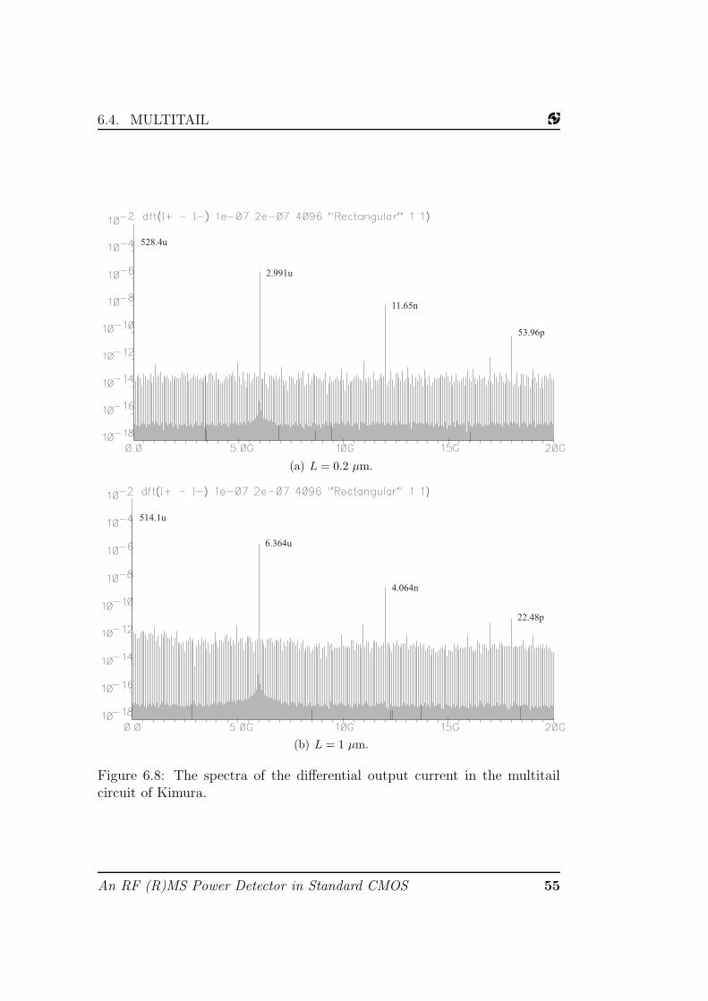
6.4. MULTITAIL
528.4u
2.991u
11.65n
53.96p
(a) L = 0.2 µm.
514.1u
6.364u
4.064n
22.48p
(b) L = 1 µm.
Figure 6.8: The spectra of the differential output current in the multitailcircuit of Kimura.
An RF (R)MS Power Detector in Standard CMOS 55

CHAPTER 6. MOS SQUARING CELLS
signal and the offset has to be subtracted by a second equal circuit for thisinput amplitude of 0.1 V. The maximum input voltage for this circuit is
vIN,max =
√4
4 + K· VGT ≈ 0.22 V (6.12)
The fourth and six harmonics, at 12 GHz and 18 GHz respectively, shouldbe as small as possible.
56 Master Thesis
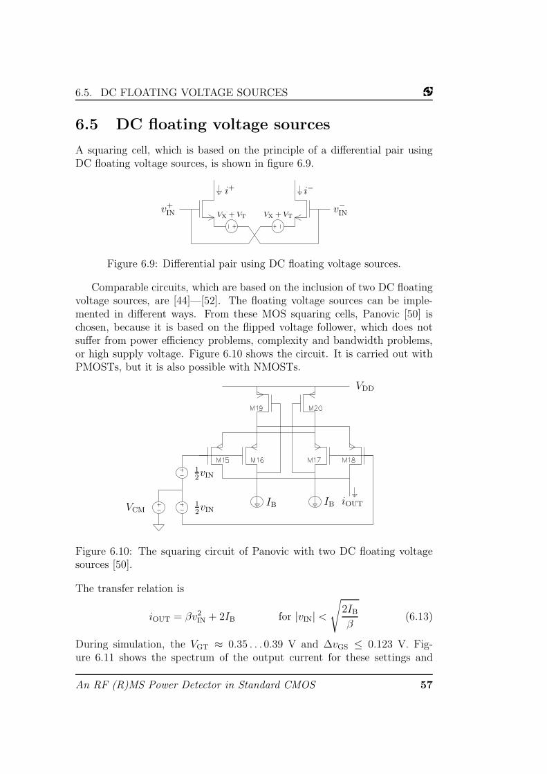
6.5. DC FLOATING VOLTAGE SOURCES
6.5 DC floating voltage sources
A squaring cell, which is based on the principle of a differential pair usingDC floating voltage sources, is shown in figure 6.9.
VX + VT VX + VT
i+ i−
v+IN v−
IN
Figure 6.9: Differential pair using DC floating voltage sources.
Comparable circuits, which are based on the inclusion of two DC floatingvoltage sources, are [44]—[52]. The floating voltage sources can be imple-mented in different ways. From these MOS squaring cells, Panovic [50] ischosen, because it is based on the flipped voltage follower, which does notsuffer from power efficiency problems, complexity and bandwidth problems,or high supply voltage. Figure 6.10 shows the circuit. It is carried out withPMOSTs, but it is also possible with NMOSTs.
IBIB iOUT
12vIN
12vINVCM
VDD
Figure 6.10: The squaring circuit of Panovic with two DC floating voltagesources [50].
The transfer relation is
iOUT = βv2IN + 2IB for |vIN| <
√2IB
β(6.13)
During simulation, the VGT ≈ 0.35 . . . 0.39 V and ∆vGS ≤ 0.123 V. Fig-ure 6.11 shows the spectrum of the output current for these settings and
An RF (R)MS Power Detector in Standard CMOS 57

CHAPTER 6. MOS SQUARING CELLS
L = 0.2 µm for all MOSTs. There is no spectrum shown for a five timeslarger W and L, because of the practical reason of very large PMOSTs.
3.053m
28.32u
111.6n
207.1p
Figure 6.11: The spectrum of the output current of Panovic.
In figure 6.11, the odd harmonics are not present in the output current.These terms are eliminated for small signals, because the circuit is carriedout differentially. The DC term contains offset and signal. The offset is,according to (6.13), twice the bias current. So, the signal part is in the orderof a milliamp and is not close to the second harmonic. This can be explainedpartly with the voltage level at the output, because this level is very close toground; this level is determined by the 1 Ω resistor, which is used to measurethe output current. This means that the signal part is usually a smaller partof the output signal and the offset has to be subtracted by a second equalcircuit for this input amplitude of 0.1 V. The fourth and six harmonics,at 12 GHz and 18 GHz respectively, should be as small as possible. Themaximum input voltage for this circuit is
vIN,max = VGT ≈ 0.35 V (6.14)
The fourth and six harmonics, at 12 GHz and 18 GHz respectively, shouldbe as small as possible.
58 Master Thesis

6.6. COMPARISON
6.6 Comparison
A comparison of the previous four ideal circuits can be made by dividing theeven power terms as shown in table 6.1.
DC/x2 x2/x4 x4/x6
W/L 5W/5L W/L 5W/5L W/L 5W/5L
Wiegerink 285 3824 285 53569 217Kimura (2UP) 151 113 99 471 97 127Kimura (MT) 177 81 257 1565 216 181Panovic 108 254 539
Table 6.1: Comparison by dividing the even power terms of the four circuits.
A good squaring cell has low factors for the DC term divided by thesecond order term. This means a small offset and small influences of thefourth and higher order harmonics. Besides, the factors for the second orderterm divided by the fourth order term should be very high to minimize thefourth and higher order terms.
Table 6.2 shows the effective input signal ∆vGS,RMS and the maximum(relative and absolute) input signal sIN,max. The maximum input signal isdefined by the (square-law) transfer relation. The ∆vGS,RMS is not equal forall circuits, because of equal input amplitudes, vIN = 0.1 V.
∆vGS,RMS sIN,max
[mV] [V]
Wiegerink 71 2VGT 0.6Kimura (2UP) 89 VGT√
K0.22
Kimura (MT) 71√
44+K
· VGT 0.22
Panovic 87 VGT 0.35
Table 6.2: Comparison of the four circuits by the input signal in relation tothe maximum input signal.
The Kimura (2UP) circuit is bad in comparison with the other three.The multitail circuit of Kimura belongs to the best, but is not clearly thebest. So, this circuit is compared in the next section with the Wiegerink andPanovic circuits by adding non-linearities.
An RF (R)MS Power Detector in Standard CMOS 59

CHAPTER 6. MOS SQUARING CELLS
6.7 Adding non-linearities
In this section, non-linearities are added to the ideal circuits of the previoussections and are discussed with simulation results, to make a good distinction.The following non-linearities are added:
• bias current via mirror;
• output current via mirror;
• feedback loop with difference-of-squares function.
With these simulations, no specs are calculated or checked.
6.7.1 Bias current via mirror
The first added non-ideality in the circuits of the previous sections is a currentmirror between the ideal bias current sources and the circuits. Figure 6.12shows these current mirrors. The reasons for this are, focussing on the head-room and including the impedance of the MOSTs.
IB
VDD
(a) Wiegerink
IB
(b) Kimura (MT)
IB
(c) Panovic
Figure 6.12: The ideal bias current sources with the current mirrors for threedifferent circuits.
The dimensions are chosen such that the DC settings are still the same(approximately) and the vGT of the diode-connected MOSTs is about 0.3 V.For some circuits, the common mode voltage at the input is changed forenough voltage headroom. A comparison of the three circuits is made andshown in table 6.3.
The factor between DC and the second order term is better for Kimura(MT) and Panovic. Wiegerink is a little bit better in suppressing the fourthorder term and Kimura (MT) is better in suppressing the six order term.Also these results are not enough to choose the best of three.
60 Master Thesis

6.7. ADDING NON-LINEARITIES
DCx2
x2
x4
x4
x6
Wiegerink 434 389 146Kimura (MT) 182 265 224Panovic 123 311 161
Table 6.3: Comparison by dividing the even power terms of the three circuitsincluding bias current mirrors for the standard bulk voltages.
6.7.2 Output current via mirror
Another non-ideality, which is added to the ideal circuits, is a current mirrorto the output current. Figure 6.13 shows the output current mirror for theKimura (MT) circuit, because of the differential output current in the basic(ideal) circuit.
iOUT
VDD
i+ i−
Figure 6.13: The current mirror for the differential output current of theKimura (MT) circuit.
The dimensions are chosen such that the DC settings are still the same(approximately) and the vGT of the diode-connected MOSTs is about 0.3 V.For some circuits, the common mode voltage at the input is changed forenough voltage headroom. The output currents are simulated via a resistorto ground or supply voltage to determine the current. Usually, the value is1 Ω, but for the Kimura (MT) is used a 1.3 kΩ resistor to the supply voltageto balance the mirror. Because when the impedance is too small, the drainof PMOST M30 is too close to the supply voltage. A comparison of the threecircuits is made and shown in table 6.4. The best suppression of the fourthand higher harmonics is realized by Kimura (MT), but the factor betweenDC and the second harmonic is much smaller and better by Panovic.
When looking at all comparisons of the squaring circuits so far, theKimura (MT) is the best and most simple squaring cell. From now on,the simulations are carried out with PSS instead of DFT, because it is easyto sweep the input amplitude.
An RF (R)MS Power Detector in Standard CMOS 61

CHAPTER 6. MOS SQUARING CELLS
DCx2
x2
x4
x4
x6
Wiegerink 295 334 301Kimura (MT) 653 636 313Panovic 142 267 131
Table 6.4: Comparison by dividing the even power terms of the three circuitsincluding output current mirrors.
6.8 Second order effects
The relation between the square root of the output current and the inputamplitude should be very linear. This is not easy to realize, because of thesecond order effects. For the circuits that were analyzed in sections 6.2–6.5,a number of non-idealities are observed. These non-idealities appear to beindependent of frequency and hence are (quasi) DC effects. The origins ofthese second order effects are investigated in this section.
The effects appear to be roughly the same for all presented circuits. Theeffects are explained with DC analyses of the Kimura (MT) squaring cell asshown in figure 6.14. This figure shows the derivative of the square root ofthe differential output current minus the DC component versus the inputamplitude for the square-law and the BSIM3 model. This means, accordingto (6.11)
∂(√
K2+K
βv2IN
)
∂ (vIN)=
√K
2 + Kβ (6.15)
The square-law curves are constant (horizontal) at this value, in the range inwhich the relation is derived. For the curves in figure 6.14, both models areused in combination with different channel lengths and overdrive voltages.The values are written beside the characteristic.
The negative slope is fixed and caused by the input MOST, when itcomes in weak inversion. So, a higher overdrive voltage moves the peakto the right, because it allows a larger input voltage range before it comesin weak inversion. The peak in the characteristic can be calculated by therequirement of equation (6.11).
The effects of the following second order effects are investigated:
• body effect;
• channel length modulation;
• mobility reduction;
62 Master Thesis

6.8. SECOND ORDER EFFECTS
VGT = 0.3 V
VGT = 0.4 V
VGT = 0.5 V
(a) Square-law model.
10W10L
= 502
5W5L
= 251
WL
= 50.2
VGT = 0.3 V
VGT = 0.4 V
VGT = 0.5 V
(b) BSIM3 model.
Figure 6.14: The derivative of the square root of the differential outputcurrent of the Kimura (MT) circuit minus the DC component as a functionof the input amplitude for different channel lengths and overdrive voltages.
An RF (R)MS Power Detector in Standard CMOS 63

CHAPTER 6. MOS SQUARING CELLS
• subthreshold conduction.
The result of each second order effect is investigated by using the square-law(basic level 1 MOS) model in SpectreHDL. With this model, it is possible toadd specific second order effects to the square-law model. The SpectreHDLfile is shown in appendix C.
6.8.1 Body effect
The body effect (γ) increases the threshold voltage and can be modelledas [53]
VT = VT0 + γ(√
|2ΦF + VSB| −√
|2ΦF|)
(6.16)
When the body effect is the only added second order effect, the idealoutput curve is changed negligibly. This means that the ideal circuit isindependent on variation of the threshold voltage, but in combination withother effects, this effect is perceptible.
6.8.2 Channel length modulation
The channel length modulation effect (λ) can be modelled as [53]
ID ≈ 1
2µnCox
W
L(VGS − VT)2(1 + λVDS) (6.17)
≈ 1
2β(VGT)2(1 + λVDS) (6.18)
Figure 6.15 shows the derivative of the square root of the differentialoutput current minus the DC component versus the input amplitude (as infigure 6.14(b)). For these curves, the square-law model is used with differentvalues of channel length modulation (λ).
The ideal curve without second order effects is horizontal till one inputMOST comes in weak inversion, as mentioned before. The channel lengthmodulation (λ) increases the starting point, because the actual length of thechannel decreases with increasing drain-source voltage. A smaller channellength results in a larger β and according to (6.15) to a larger starting point.
6.8.3 Mobility degradation
The third second order effect which is investigated, is the mobility degrada-tion (θ). The mobility reduces for small devices and considerably for over-drive voltages above 100 mV [53]. So, this effect is clearly perceptible in
64 Master Thesis

6.8. SECOND ORDER EFFECTS
Figure 6.15: The derivative of the square root of the output current of theKimura (MT) circuit minus the DC component as a function of the inputamplitude with the square-law model for different λ.
figure 6.16. Figure 6.16 shows the derivative of the square root of the differ-ential output current minus the DC component versus the input amplitude(as in figure 6.14(b)). For these curves, the square-law model is used withdifferent values of mobility reduction (θ).
For the vertical field, this effect can be modelled as [53]
µeff =µ0
1 + θ · vGT
(6.19)
and in combination with the lateral field1
µeff =µ0
1 +(
µ0
2vsatL+ θ)
vGT
(6.20)
where θ ≈ 10−9
tox [m]. From equation (6.20), it is clear that the overdrive voltage
and the channel length both influence the mobility degradation and thiscorresponds with figure 6.14(b).
According to (6.20), the mobility degradation can be reduced by longer
1Also known as velocity saturation.
An RF (R)MS Power Detector in Standard CMOS 65

CHAPTER 6. MOS SQUARING CELLS
Figure 6.16: The derivative of the square root of the output current of theKimura (MT) circuit minus the DC component as a function of the inputamplitude with the square-law model for different θ.
channels. For the used channel lengths in the previous sections, this means
µeff =0.035
1 +(
0.0352·105·L + 10−9
4.2·10−9
)vGT
[m2
Vs
]
=0.035
1 + (0.875 + 0.238) vGTfor L = 0.2 µm
=0.035
1 + (0.175 + 0.238) vGTfor L = 1 µm
6.8.4 Subthreshold conduction
The fourth second order effect which is investigated, is the subthreshold con-duction. This effect describes the weak inversion behavior, which occurs whenthe overdrive voltage is very small or even negative and can be formulatedby [53]
ID = I0 · eqVGSkTζ (6.21)
where ζ > 1 is a non-ideality factor.The planed peaks of figure 6.14(b) are a result of the subthreshold conduc-
tion. The subthreshold conduction is not included in the square-law model,which causes the sharp transitions of figures 6.15 and 6.16.
66 Master Thesis
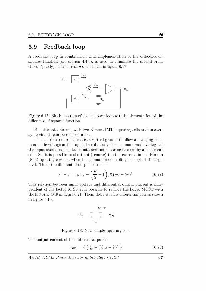
6.9. FEEDBACK LOOP
6.9 Feedback loop
A feedback loop in combination with implementation of the difference-of-squares function (see section 4.4.3), is used to eliminate the second ordereffects (partly). This is realized as shown in figure 6.17.
x2
x2
CAV
+
-iREF
iSQR
sIN
sOUT
iERRP
Figure 6.17: Block diagram of the feedback loop with implementation of thedifference-of-squares function.
But this total circuit, with two Kimura (MT) squaring cells and an aver-aging circuit, can be reduced a lot.
The tail (bias) current creates a virtual ground to allow a changing com-mon mode voltage at the input. In this study, this common mode voltage atthe input should not be taken into account, because it is set by another cir-cuit. So, it is possible to short-cut (remove) the tail currents in the Kimura(MT) squaring circuits, when the common mode voltage is kept at the rightlevel. Then, the differential output current is
i+ − i− = βv2IN −
(K
2− 1
)β(VCM − VT)2 (6.22)
This relation between input voltage and differential output current is inde-pendent of the factor K. So, it is possible to remove the larger MOST withthe factor K (M9 in figure 6.7). Then, there is left a differential pair as shownin figure 6.18.
iOUT
v+IN v−
IN
Figure 6.18: New simple squaring cell.
The output current of this differential pair is
iOUT = β(v2IN + (VCM − VT)2
)(6.23)
An RF (R)MS Power Detector in Standard CMOS 67
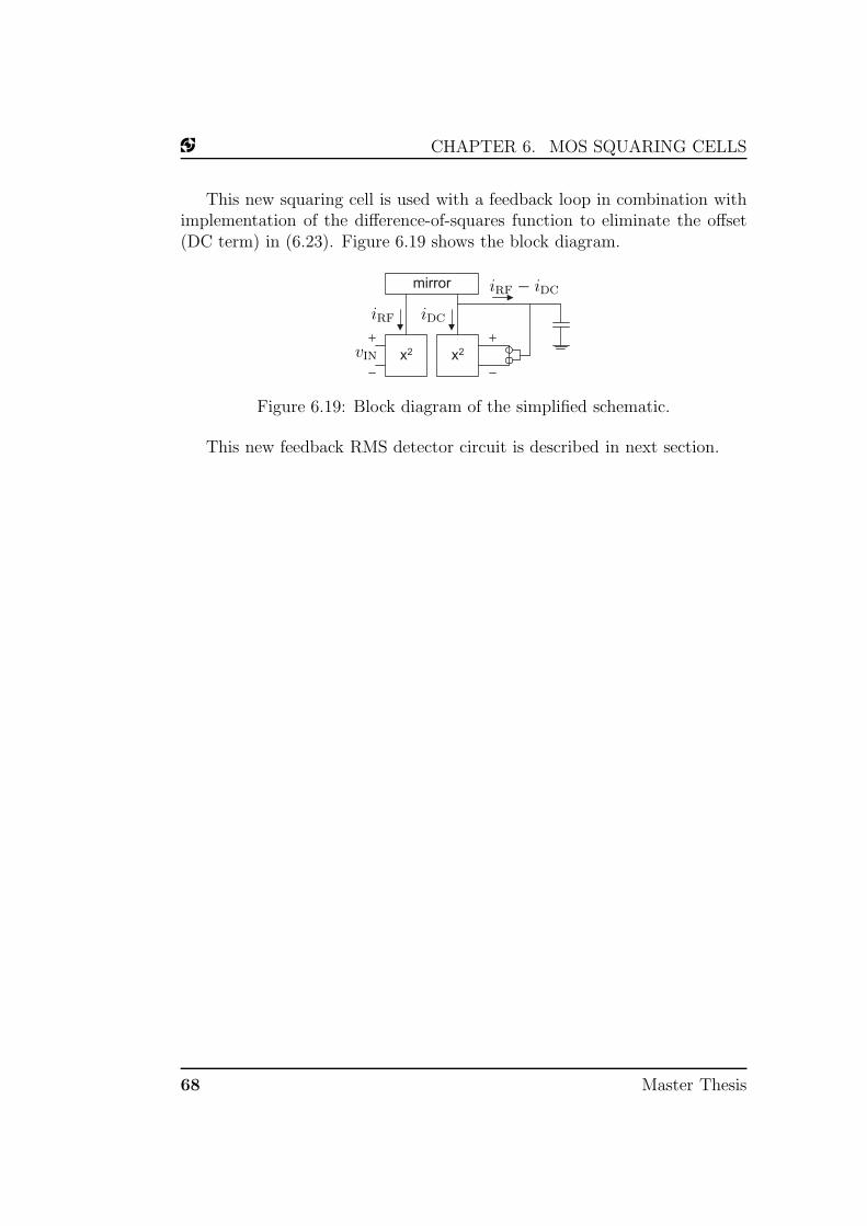
CHAPTER 6. MOS SQUARING CELLS
This new squaring cell is used with a feedback loop in combination withimplementation of the difference-of-squares function to eliminate the offset(DC term) in (6.23). Figure 6.19 shows the block diagram.
mirror
x2 x2
iRF iDC
iRF − iDC
vIN
Figure 6.19: Block diagram of the simplified schematic.
This new feedback RMS detector circuit is described in next section.
68 Master Thesis

6.10. FEEDBACK RMS DETECTOR CIRCUIT
6.10 Feedback RMS detector circuit
Figure 6.20 shows the schematic of this complete new very simple circuit.The current mirror on top of the squaring cells, as shown in figure 6.19, is
implemented as a folded cascode, which increases the output resistance andkeeps the drain voltages of both squaring cells equal. The voltage headroomis enough, because of using PMOSTs and NMOSTs.
The two uppermost PMOSTs (M1 and M2) function as constant currentsources. The drain current of PMOST M3 (ID,3) is equal to the drain currentof PMOST M1 minus the square current, which flows through NMOSTs M7and M8. ID,3 is mirrored by NMOSTs M5 and M6. This mirrored current ID,4
is exactly the same as ID,3, because of equal NMOSTs and the drain voltagesare kept equal by the operational amplifier. This forces equal currents flowingthrough both squaring cells.
The averaging circuit in the feedback loop is realized by an integrator,here implemented as an operational amplifier with a capacitor2 in its feedbackloop. The open loop gain of the operational amplifier is set to 105. Thisaveraging circuit is only simulated in combination with a sine wave inputvoltage. So, it is possible that this averaging circuit is not the best for a verycomplex signal, e.g. CDMA.
In the feedback loop are two ideal voltage controlled voltage sources totransfer the output voltage to a differential voltage. Quasi-DC operationimplementable with e.g. an operational amplifier.
The bias currents are set to 500 µA. PMOSTs M11 and M12 produce thebias voltages for PMOSTs M1 to M4. NMOST M13 provides the commonmode input voltage for both squaring cells.
The dimensions and overdrive voltages of all MOSTs in the feedback RMSdetector circuit are specified in table 6.5.
W [µm] L [µm] VGT [V]
M1, M2, M11 50 0.2 0.19M3, M4 30 0.5 0.27M5, M6 3 1 0.71M7, . . ., M10 2.5 1 0.68M12 6 0.2 0.67M13 3 0.2 0.57
Table 6.5: Dimensions and overdrive voltages of all MOSTs in the feedbackRMS detector circuit.
2This capacitor has a value of 3 fF, which is a very small capacitance. It also workswith a much larger capacitance, but a small value results in much faster PSS simulations.
An RF (R)MS Power Detector in Standard CMOS 69

CHAPTER 6. MOS SQUARING CELLS
I BI B
vO
UT
vIN
VC
M
VC
M
VC
M
VD
D
VB
1VB
1
VB
2
VB
2
Figure 6.20: Feedback RMS detector circuit.
70 Master Thesis

Chapter 7
Results
This chapter shows the results of the feedback RMS detector circuit for thespecifications in subsection 5.1.7:
• operating frequency;
• dynamic range;
• supply voltage;
• operating temperature;
• supply current;
• non quasi static behavior;
• mismatch.
These specifications are all verified for a sine waveform and not for a verycomplex signal, e.g. CDMA, because it is not easy to generate such wave-forms in Cadence. The timing parameters and the relative power accuracyare not verified, because it was difficult to control the input power.
For benchmarking purposes, frequently a comparison is made with theKimura (MT)-based circuit, which contains two Kimura (MT) squaring cellsand a feedback loop. The schematic of this Kimura (MT)-based circuit isshown in figure D.1 in appendix D.
An important point of attention is that the absolute accuracy appears inall items and is only checked for every spec separately.
71

CHAPTER 7. RESULTS
7.1 Linearity
In the first place a comparison is made between the Kimura (MT)-based andthe feedback RMS detector circuit, based on the linearity. This is carriedout by DC and PSS simulations at the output current of one squaring cell(without feedback loop) and at the output voltage in the feedback loop withtwo squaring cells. Figure 7.1 shows the results of these simulations. On theleft vertical axis are shown the DC and PSS simulation of the output currentof one squaring cell (without feedback loop). From these simulations, thesquare root and the derivative are taken successively. On the right verticalaxis are shown the DC and PSS simulation of the output voltage of thefeedback loop with two squaring cells. From these simulations, only thederivative is taken. So all curves should be horizontal.
The DC input amplitude is increasing to 1 V and the PSS input amplitudeis increasing to 1.5 V, because of the factor
√2 difference of input power.
The output voltage of the feedback loop should be 1 V for the DC simulationand 1
2
√2 V for the PSS simulation. Furthermore the maximum difference of
the gate source voltage in both circuits is the input amplitude.Figure 7.1(a) shows that the DC simulation of the Kimura (MT)-based
circuit with feedback loop is much better than without feedback loop. ThePSS simulation is also improved, when looking at the first positive slope.
Figure 7.1(b) shows that the DC simulation of the feedback RMS detectorcircuit with feedback loop is very good. Without the feedback loop is thefeedback RMS detector circuit much better than the Kimura (MT)-basedcircuit. The PSS simulation is also improved, when looking at the firstpositive slope. Even at a high input, the deviation is acceptable, but thesquare-law relation is valid for an input amplitude smaller than 1 V.
So when comparing the Kimura (MT)-based and the feedback RMS de-tector circuit, the feedback RMS detector circuit is clearly much better forboth types of implementation.
72 Master Thesis
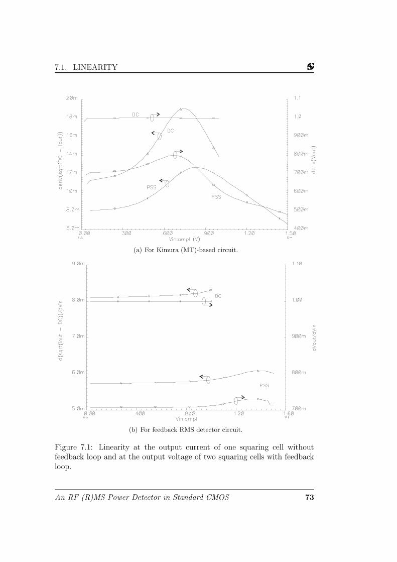
7.1. LINEARITY
(a) For Kimura (MT)-based circuit.
(b) For feedback RMS detector circuit.
Figure 7.1: Linearity at the output current of one squaring cell withoutfeedback loop and at the output voltage of two squaring cells with feedbackloop.
An RF (R)MS Power Detector in Standard CMOS 73

CHAPTER 7. RESULTS
7.2 Operating frequency
In this section, the frequency dependency of the circuits is examined. Theoperating frequency should be varied from 400 MHz to 3 GHz, according tothe specs. Figure 7.2 shows the performance of the feedback RMS detectorcircuit in relation with the operating frequency. In this figure, the capacitancevalue (displayed at the top of the figure) of the integrator varies with thefrequency to show that the minimum frequency determines the capacitorvalue1. On the left vertical axis is plotted the output voltage and on the
Figure 7.2: Frequency dependency of output voltage for the feedback RMSdetector circuit.
right vertical axis is plotted the output voltage divided by the input voltagein decibels (error). Both as a function of the input amplitude. It is clear thatthe plot comply with the specs for the absolute accuracy of ±1 dB. Whenthe capacitor is variable, the error is ±0.04 dB.
1For the highest frequency, the circuit also works with a larger capacitance, but a smallvalue results in much faster PSS simulations.
74 Master Thesis
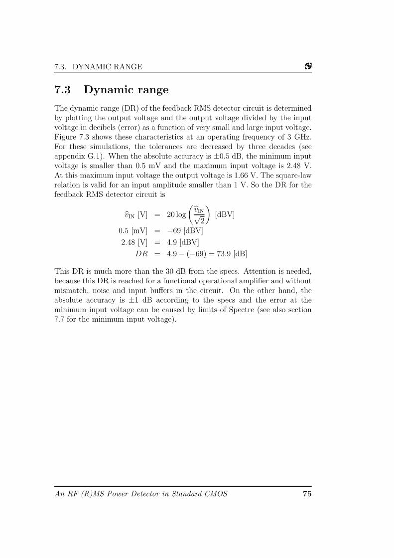
7.3. DYNAMIC RANGE
7.3 Dynamic range
The dynamic range (DR) of the feedback RMS detector circuit is determinedby plotting the output voltage and the output voltage divided by the inputvoltage in decibels (error) as a function of very small and large input voltage.Figure 7.3 shows these characteristics at an operating frequency of 3 GHz.For these simulations, the tolerances are decreased by three decades (seeappendix G.1). When the absolute accuracy is ±0.5 dB, the minimum inputvoltage is smaller than 0.5 mV and the maximum input voltage is 2.48 V.At this maximum input voltage the output voltage is 1.66 V. The square-lawrelation is valid for an input amplitude smaller than 1 V. So the DR for thefeedback RMS detector circuit is
vIN [V] = 20 log
(vIN√
2
)[dBV]
0.5 [mV] = −69 [dBV]
2.48 [V] = 4.9 [dBV]
DR = 4.9 − (−69) = 73.9 [dB]
This DR is much more than the 30 dB from the specs. Attention is needed,because this DR is reached for a functional operational amplifier and withoutmismatch, noise and input buffers in the circuit. On the other hand, theabsolute accuracy is ±1 dB according to the specs and the error at theminimum input voltage can be caused by limits of Spectre (see also section7.7 for the minimum input voltage).
An RF (R)MS Power Detector in Standard CMOS 75

CHAPTER 7. RESULTS
(a) Small input voltage
(b) Large input voltage
Figure 7.3: Dynamic range for the feedback RMS detector circuit.
76 Master Thesis

7.4. SUPPLY VOLTAGE
7.4 Supply voltage
This section shows the supply voltage dependency of the circuits. The supplyvoltage is 1.8 V, but may vary ±10%. According to the specs, the simulationsare carried out for supply voltages between 1.6 and 2.0 V.
Figure 7.4 shows these characteristics for the Kimura (MT)-based andthe feedback RMS detector circuit at an operating frequency of 3 GHz.
On the left vertical axis is shown the output voltage and on the rightvertical axis is shown the output voltage divided by the input voltage indecibels (error). These error curves should be smaller than ±1 dB. Whenpaying attention to the condition in (6.11), vIN ≤ 0.8 V (defined as VGT < 0),and changing the zero dB point, the error of the Kimura (MT)-based is about±0.35 dB. When looking at the error curves of the feedback RMS detectorcircuit, it is clear that it is much better than the Kimura (MT)-based. Whenchanging the zero dB point, the maximum error for the complete supplyvoltage range is smaller than ±0.045 dB. So for the complete supply voltagerange, it seems that both circuits meet the specs.
An RF (R)MS Power Detector in Standard CMOS 77

CHAPTER 7. RESULTS
(a) For Kimura (MT)-based circuit.
(b) For feedback RMS detector circuit.
Figure 7.4: Supply voltage dependency of output voltage for Kimura (MT)-based and feedback RMS detector circuit.
78 Master Thesis

7.5. OPERATING TEMPERATURE
7.5 Operating temperature
This section shows the temperature dependency of the circuits. Usuallythe (room) temperature is 27 C (300 K), but may vary over a large range.According to the specs, the simulations are carried out for temperaturesbetween -40 and 85 C.
Figure 7.5 shows these characteristics for the Kimura (MT)-based and thefeedback RMS detector circuit at an operating frequency of 3 GHz. Thesefigures are the same as figure 7.4, but now for different temperatures insteadof different supply voltages. The errors are in the same order as for thesupply voltage range.
Again, the error curves of the feedback RMS detector circuit are muchbetter than the Kimura (MT)-based. For the feedback RMS detector circuit,the maximum error for the temperature range is ±0.04 dB. So, also for thecomplete temperature range, it seems that both circuit meets the specs.
7.5.1 Supply current
Figure 7.6 shows the supply current versus the supply voltage of the Kimura(MT)-based and the feedback RMS detector circuit for the whole tempera-ture range at an operating frequency of 3 GHz. The bias currents are notminimized, but it is clear that the supply current can be keep smaller than10 mA. It is also obvious that the total bias currents can decrease, because theKimura (MT)-based uses two separate current sources for RF and DC part,and the feedback RMS detector circuit uses two separate current sources fortwo different bias voltages.
An RF (R)MS Power Detector in Standard CMOS 79

CHAPTER 7. RESULTS
(a) For Kimura (MT)-based circuit.
(b) For feedback RMS detector circuit.
Figure 7.5: Temperature dependency of output voltage for Kimura (MT)-based and feedback RMS detector circuit.
80 Master Thesis

7.5. OPERATING TEMPERATURE
(a) For Kimura (MT)-based circuit.
(b) For feedback RMS detector circuit.
Figure 7.6: Supply current as a function of supply voltage for the whole tem-perature range for Kimura (MT)-based and feedback RMS detector circuit.
An RF (R)MS Power Detector in Standard CMOS 81

CHAPTER 7. RESULTS
Figure 7.7: MOSTs with shorter channel length in series for NQS effects.
7.6 Non-quasi-static effects
The non-quasi-static (NQS) effects of the feedback RMS detector circuit areinvestigated in this section, because a large channel length is needed for smallmobility degradation and this results in a low cut-off frequency (fT). WhenfT is small, the QS model is not valid anymore and the MOST shows NQSbehavior.
The NQS effect is investigated by replacing the MOSTs of both squaringcells by an equivalent circuit of more MOSTs with shorter channels. Thechannel length of 1 µm is divided to smaller units in series, namely fourtimes 0.25 µm, as shown in figure 7.7. This increases the fT by a factor ofnine.
These MOSTs have not all junction capacitances separately. Drain diffu-sion area and periphery are only used by the MOST on the top and the sourcediffusion area and periphery are only used by the MOST on the bottom.
Figure 7.8 shows the derivative of the output voltage as a function ofthe input amplitude for the feedback RMS detector circuit at an operatingfrequency of 3 GHz. The square-law relation is valid for an input amplitudesmaller than 1 V. The curve with the NQS label is from the circuit with theMOSTs split up. Both curves should be horizontal. To show the difference,the curves are zoomed in. So, the NQS effect is very small (millivolts).
82 Master Thesis

7.7. MISMATCH
Figure 7.8: NQS effects at the derivative of the output voltage of the feedbackRMS detector circuit.
7.7 Mismatch
In this section, the mismatch is calculated at the output of the feedbackRMS detector circuit (as shown in figure 6.20). The mismatch is split upin threshold voltage mismatch (σ∆VT) and current factor mismatch (σ∆β/β).These can be calculated by
σ∆VT =AVT√W · L
[mV] (7.1)
σ∆β/β ≈ Aβ√W · L
[%] (7.2)
The estimated values, used for the proportionality factors, are
AVT = 4.2 mV·µm
Aβ = 2% µm
Table 7.1 shows properties and mismatch calculations of the MOSTs inthe feedback RMS detector circuit.
An RF (R)MS Power Detector in Standard CMOS 83

CHAPTER 7. RESULTS
M1/M2 M3/M4 M5/M6 M7. . .M10
W [µm] 50 30 3 2.5L [µm] 0.2 0.5 1 1gm [mΩ−1] 4.17 1.11 0.40 0.33VGT [V] 0.19 0.27 0.71 0.68σ∆VT [mV] 1.3 1.1 2.4 2.7σ∆β/β [%] 0.6 0.5 1.2 1.3
Table 7.1: Properties and mismatch calculations of MOSTs in feedback RMSdetector circuit.
For the DC squaring cell (M9 and M10) with using (6.23), the relation is
∆IOUT =
∣∣∣∣∂IOUT
∂VOUT
∣∣∣∣∆VOUT (7.3)
= 2βVOUT · ∆VOUT (7.4)
∆VOUT =∆IOUT
2βVOUT(7.5)
When assuming that the operational amplifier has an infinity gain, the thresh-old voltage mismatch of M7 yields at the output voltage
∆VOUT,7 =σ∆VT,7 · gm,7
2β9VOUT
= σ∆VT,7 ·VGT,9
2VOUT(7.6)
For M1, it yields
∆VOUT,1 =σ∆VT,1 · gm,1
2β9VOUT
= σ∆VT,1 ·gm,1 · VGT,9
gm,9 · 2VOUT(7.7)
84 Master Thesis

7.7. MISMATCH
The threshold voltage mismatches together yield at the output voltage
∆V 2OUT = 2∆V 2
OUT,1 + 2∆V 2OUT,3 + 2∆V 2
OUT,5 + 4∆V 2OUT,7
= 2σ2∆VT,1
(gm,1 · VGT,9
gm,9 · 2VOUT
)2
+ 2σ2∆VT,3
(gm,3 · VGT,9
gm,9 · 2VOUT
)2
+ . . .
+ 2σ2∆VT,5
(gm,5 · VGT,9
gm,9 · 2VOUT
)2
+ 4σ2∆VT,7
(VGT,9
2VOUT
)2
=
(AVT · VGT,9
gm,9 · VOUT
)2( g2m,1
2(WL)1
+g2m,3
2(WL)3
+g2m,5
2(WL)5
+g2m,7
(WL)7
)
≈(
4.2 · 10−3 · 0.68
0.33 · VOUT
)2((4.17)2
20+
(1.11)2
30+
(0.4)2
6+
(0.33)2
2.5
)
≈(
75 · 10−6
V 2OUT
)(0.87 + 0.04 + 0.03 + 0.04
)
≈ 73.5 · 10−6
V 2OUT
An RF (R)MS Power Detector in Standard CMOS 85

CHAPTER 7. RESULTS
The current factor mismatch of M1 yields at the output voltage
∆VOUT,1 =σ∆β/β,1 · ID,1
2β9VOUT
=σ∆β/β,1
4VOUT· gm,1
gm,9· VGT,1 · VGT,9 (7.8)
The current factor mismatches together yield at the output voltage
∆V 2OUT = 2∆V 2
OUT,1 + 2∆V 2OUT,3 + 2∆V 2
OUT,5 + 4∆V 2OUT,7
=
(AVT · VGT,9
2gm,9 · VOUT
)2(g2m,1V
2GT,1
2(WL)1+
g2m,3V
2GT,3
2(WL)3+
g2m,5V
2GT,5
2(WL)5+ . . .
+g2m,7V
2GT,7
(WL)7
)
≈(
2% · 0.68
2 · 0.33 · VOUT
)2((4.17)2(0.19)2
20+
(1.11)2(0.27)2
30+ . . .
+(0.4)2(0.71)2
6+
(0.33)2(0.68)2
2.5
)
≈(
425 · 10−6
V 2OUT
)(0.031 + 0.003 + 0.013 + 0.020
)
≈ 28.5 · 10−6
V 2OUT
The total offset voltage at the output voltage of the feedback RMS detectorcircuit is
∆VOUT =
√(73.5 + 28.5) · 10−6
V 2OUT
≈ 10
VOUT[mV]
From the mismatch calculations can be concluded, that the mismatchreduces by optimizing M1, because the M1 responsible parts are much largerthan the other. When L of PMOST M1 (and M2, M11) is increased from0.2 µm to 0.75 µm, the output resistance is maximized. The M1 responsibleparts in the mismatch calculations are related to the length as
g2m,1
2(WL)1∼ 1
L3(7.9)
So, the M1 responsible parts are reduced a lot and the total offset voltage atthe output voltage of the feedback RMS detector circuit is halved.
86 Master Thesis

7.7. MISMATCH
This means for the output voltage
∆VOUT < εmax · VOUT ≈ 10% · VOUT
5 · 10−3
VOUT
< 10% · VOUT
VOUT >√
50 · 10−3
> 224 mV ≈ −13 dBV
So, the minimum input voltage, which is investigated in section 7.3, cannot be achieved. The mismatch reduces the DR of the circuit from more than70 dB (for ±0.5 dB without mismatch) to 20 dB (for ±1 dB with mismatch).
Because the specification for the DR is 30 dB, the mismatch should bereduced. This can be done by spending area, higher gain between input andoutput voltage, which results in a higher output voltage for a small input,or by using active (digital) offset cancellation techniques. Digital circuitscan be used, because the PD is realized in a standard CMOS process. Thecancellation techniques seems to be the best possibility, because for increasingthe DR with 10 dB, the area should be increased by a factor of ten and ahigher input-output gain decreases the maximum input voltage.
An RF (R)MS Power Detector in Standard CMOS 87

CHAPTER 7. RESULTS
88 Master Thesis

Chapter 8
Conclusion
This report presents the results of research into the feasibility of RF (R)MSpower detectors for 3G in standard CMOS. The emphasis is on the identifi-cation of fundamental limitations of CMOS (here National Semiconductors’CMOS9) and of a number of squaring circuits for this specific application,rather than to meet the target specifications.
The main research question is:
What are the boundaries of a standard CMOS process for thisapplication and why?
A literature study showed that for 3G RF power detectors a true (R)MSdetector is required, which consists of at least one squaring cell and an aver-aging circuit. It is shown that the squarer does not have to be ideal: all oddharmonics are allowed, because they are filtered out by the averaging circuit.Also higher even harmonics are allowed, as long as the resulting residual er-ror is sufficiently small. A DC output signal is allowed only if it is effectivelyeliminated using e.g. a feedback loop including an identical squarer cell orwith a kind of offset calibration.
CMOS squarer cells in literature can be categorized into four classes. Outof each class of squarer, one circuit implementation is selected for benchmark-ing: the Wiegerink [35], the Kimura (2UP) [47], the Kimura (MT) [47] andthe Panovic [50]. Of these four, the Kimura (MT) belongs to the best andis the most simple circuit but still has serious drawbacks in terms of e.g.linearity.
Under assumption of a well defined common mode input voltage level,the Kimura (MT) circuit can be improved/simplified considerably. Based onthis improved circuit, a new circuit topology including a DC feedback loopwas created: the feedback RMS detector circuit. The performance of this
89

CHAPTER 8. CONCLUSION
circuit is much better than that of the other squarer circuits; the presentedsimulations results meet the specifications for 3G RF power detectors.
According to (PSS and DC) simulations, the presented feedback RMSdetector
• is suitable for the complete frequency range from 400 MHz to 3 GHz.The averaging circuit partly determines the lower bound to this range.High bandwidth operation is possible with relatively long transistor,because only a quasi-DC output signal is required;
• can have a large dynamic range, upper bound by mainly moderate-inversion effects and lower bound by mainly mismatch (offset) issues.This mismatch related error is 10
VOUT[mV] for the presented circuit. The
DR increases above 20 dB by spending area. The mismatch should bereduced further by using active (digital) offset cancellation techniquesto increase the DR up to 30 dB;
• can be operated on low supply voltages. Thus to the absence of e.g.tail currents the voltage headroom of all the transistors in the feed-back RMS detector circuit is relatively large. Using a balanced circuittopology, the effect of supply variations is small;
• is fairly insensitive to temperature variations. This is due to again thebalanced circuit topology and the usage of a DC feedback loop withidentical components as in the RF path, thereby effectively cancellingtemperature dependencies of the components;
• requires input signals with a well defined (easy to define) DC level;
• has an arbitrarily set current consumption of 2 mA, without inputbuffers and in-loop operational amplifier.
The simulations are done using BSIM3 models, which are not very accurate inmoderate inversion and if NQS behavior occurs. In the presented circuit, theMOS transistors are operated on relatively large effective gate-source over-drive voltages, which ensures fair modelling with BSIM3 from input signallevels up to almost maximum input signal levels. The NQS effects on the cir-cuit performance is expected to be small, because they mainly induce delaysand filtering effects that do not harm the circuit performance; simulationsverify this expectation.
In conclusion, it appears to be feasible to integrate RF (R)MS powerdetectors in standard CMOS. The feedback RMS detector circuit seems tobe well suited for this purpose; the linear input buffers (RF and DC) and theloop filter are still to be designed.
90 Master Thesis

Chapter 9
Recommendations
Because the time for this study is not infinity, there are some recommenda-tions left for supporting, verifying or getting better results. All items aresummed below and could be useful to do.
Type of input signal The input signal used at all simulations is a sinewave at a certain frequency. The PD should be used in an applicationwith CDMA signals. So, the circuit should be checked for this kind ofsignals.
Optimum bias currents The bias currents are not optimized. The biascurrents are chosen and the circuit is adjusted at this current. Howeverthe bias currents can be smaller, but the minimum bias current has notto be the optimum bias current. So, the optimum bias current shouldbe determined for saving power probably and maybe a better workingcircuit.
Transistor-size unbalance technique The circuit, based on the transistor-size unbalance technique, is rejected by the spectrum. This is not thebest and fairest manner. Maybe the circuit has other advantages orcan be adjusted better.
DC floating voltage sources The circuit, based on the DC floating volt-age sources is rejected later on. It was not a bad circuit, but it haslarge PMOSTs and is hard to adjust. The large MOSTs can be relatedto a large bias current. So, find the optimum of this circuit realizedwith NMOSTs and compare it with the other.
Relative accuracy Many specs are checked in chapter 7. Also the absoluteaccuracy, but not the relative accuracy. Most likely, this spec is alsoreached and the feedback RMS detector circuit still keep the best.
91

CHAPTER 9. RECOMMENDATIONS
Averaging As mentioned in chapter 5, the averaging is leaving out. But inthe next chapter, there is averaging used for the feedback loop. Thisaveraging is determined by some simulations and is not optimized. Thekind of filter and the values of capacitors, resistors and open loop gainhave to be determined. So the best averaging circuit should be calcu-lated for this application.
Mismatch For the feedback RMS detector circuit, the mismatch is onlycalculated and not simulated. So, for a better approach of the mis-match, it should be included within the simulation. The (calculated)mismatch is too large and should be reduced by spending area and byusing active (digital) offset cancellation techniques. Digital circuits canbe used, because the PD is realized in a standard CMOS process.
Operational amplifier All the results of the feedback RMS detector circuitare based on a functional operational amplifier. This one should bereplaced by a operational amplifier circuit and makes it possible to usethe schematic. Maybe the results are a little bit worse.
92 Master Thesis

Appendix A
Available RMS detectors
Below are listed some available RMS detectors from Analog Devices andNational Semiconductor.
Note: For the mentioned specs, not all conditions are exactly the samefor different parts, but the values are a good indication.
Table A.1: Specs of available RMS detectors.Part# VDD IDD fRF DR Accuracy
[V] [mA] [Hz] [dB]a [dB]
AD8361 [24] 2.7–5.5 (3) 1.1 0-2.5G 14/23/26 ±0.25/1/2AD8362 [28] 4.5–5.5 (5) 20 50–2.7G >60/63 ±0.5/1ADL5500 [29] 2.7–5.5 (5) 1 0.1G–6G 23/30/32 ±0.25/1/2LMV232b [30] 2.5–3.3 (2.7) 9.8 50M–2G 24/29 ±0.5/1
aInput: CW @ 900 MHzbIs a Dual-Channel Mean-Square Detector.
A.1 AD8362
In this appendix, the existent IC AD8362 is demonstrated. The functionaldiagram is shown in figure A.1. The input signal is applied to a linear-in-dB VGA, which includes a voltage controlled (resistive ladder) attenuator.The output of the VGA is measured by an accurate square law detector,which provides a true RMS response to the entered alternating signal. Theoutput current of the HF squaring cell is integrated by the capacitance CF.The resulting voltage is buffered and gained by an error amplifier. Thefluctuating current is balanced against a fixed target current using current
93

APPENDIX A. AVAILABLE RMS DETECTORS
mode subtraction. This second current is provided by a second squaring cell,which is driven by a fraction of a fixed reference voltage vREF. The attenuatedreference voltage determines the output that has to be provided by the VGA.Both squaring cell output voltages have to be equal. The output signal, whichis produced by the error amplifier is applied to the gain control input of theVGA and forms an AGC loop. This loop can be realized internally via asetpoint interface for configuration in a measurement mode, but the loopcan also be realized externally via the PA and the coupler for configurationin a controller mode, as in figure 4.13(b). The VGA gain control transferfunction is negative, i.e. an increasing voltage decreases the gain. The RMSoutput voltage is proportional to the logarithm of the RMS value of the input(linear-in-dB). For more details, see [10, 28, 25].
x2
x2
error
amp.
CF
VGA
setp.
intrf.
x 0.06
vIN
vREF
vOUT
vCTRL P
Figure A.1: Block diagram of the RMS responding detector AD8362.
Temperature stability and linearity of this RMS detector can be improvedby some techniques [10]. The accuracy is increased with simple techniqueswhich use resistors, capacitors and a temperature sensor.
94 Master Thesis

Appendix B
Taylor series of some commonfunctions
The hyperbolic functions (sinh, tanh, arcsinh and arctanh) are not listed,because they have almost the same Tailor series as the summed trigonometricfunctions.
sin x =∞∑
n=0
(−1)n
(2n + 1)!x2n+1
= x − x3
3!+
x5
5!− x7
7!+ . . . ∀x ∈ R
tan x =
∞∑
n=1
B2n(−4)n(1 − 4n)
(2n)!x2n−1
= x +1
3x3 +
2
15x5 +
17
315x7 + . . . for |x| <
π
2
arcsin x =
∞∑
n=0
(2n)!
4n(n!)2(2n + 1)x2n+1
= x +2!
12x3 +
4!
320x5 +
6!
16128x7 + . . . for |x| < 1
arctan x =
∞∑
n=0
(−1)n
2n + 1x2n+1
= x − x3
3+
x5
5− x7
7+ . . . for |x| < 1
ex − e−x =
∞∑
n=0
xn
n!−
∞∑
n=0
(−x)n
n!
= 2x + 2x3
3!+ 2
x5
5!+ 2
x7
7!+ . . . ∀x ∈ R
95

APPENDIX B. TAYLOR SERIES OF SOME COMMON FUNCTIONS
96 Master Thesis

Appendix C
Basic level 1 MOS model(SpectreHDL)
#define EPS0 8.8541879239442001396789635e-12
#define EPS_OX 3.9*EPS0/100.0
// mos level-1 model (kinda).
#define F1(m, f, v) ((v/(1 - m))*(1 - pow((1 - f), m)))
#define F2(m, f) (pow((1 - f), (1 + m)))
#define F3(m, f) (1 - f*(1 + m))
module mos1(drain, gate, source, body) (w, l, as, ad, pd, ps)
node [V, I] drain, gate, source, body;
parameter real w = 1 from (0:inf);
parameter real l = 1 from (0:inf);
parameter real as = 1 from (0:inf);
parameter real ad = 1 from (0:inf);
parameter real pd = 1 from (0:inf);
parameter real ps = 1 from (0:inf);
// model parameters
parameter real vto = 0.4 from (0:inf);
parameter real gamma = 0 from [0:inf);
parameter real phi = 0.35 from (0:inf);
parameter real lambda = 0.5 from [0:inf); //0.1,..,0.35,..,0.5
parameter real lambda2 = 0 from [0:inf);
parameter real theta = 1.1 from [0:inf); //0.4,..,1.1
parameter real tox = 4.2e-7 from (0:inf);
parameter real u0 = 350 from (0:inf);
parameter real xj = 0 from [0:inf);
parameter real is = 1e-20 from (0:inf);
97

APPENDIX C. BASIC LEVEL 1 MOS MODEL (SPECTREHDL)
parameter real cj= 0 from [0:inf); //3e-15
parameter real vj=0.75 exclude 0;
parameter real mj=0.5 from [0:1);
parameter real fc=0.5 from [0:1);
parameter real tau = 0 from [0:inf);
parameter real cgbo = 42e-17 from [0:inf);
parameter real cgso = 6e-15 from [0:inf);
parameter real cgdo = 46e-17 from [0:inf);
parameter integer type=1 from [-1:1];
// visible variables.
export real vds, vgs, vbs, vbd, vgb, vgd, vth, id, ibs,
ibd, qgb, qgs, qgd, qbd, qbs;
real kp, fc1, fc2, fc3, fpb, leff, beta;
initial
leff = l - 2*xj;
kp = u0*EPS_OX/tox;
fc1 = F1(mj, fc, vj);
fc2 = F2(mj, fc);
fc3 = F3(mj, fc);
fpb = fc*mj;
analog
vds = type*V(drain, source);
vgs = type*V(gate, source);
vgb = type*V(gate, body);
vgd = type*V(gate, drain);
vbs = type*V(body, source);
vbd = type*V(body, drain);
if (vbs > 2*phi)
vth = vto + gamma*sqrt(2*phi);
else
vth = vto - gamma*(sqrt(2*phi - vbs) - sqrt(2*phi));
// parasitic diodes...
ibd = is*(exp(vbd/$vt()) - 1);
ibs = is*(exp(vbs/$vt()) - 1);
if (vbd <= fpb)
qbd = tau*ibd + cj*vj*(1 - pow((1 - vbd/vj),
(1 - mj)))/(1 - mj);
else
qbd = tau*ibd + cj*(fc1 + (1/fc2)*(fc3*(vbd - fpb) +
98 Master Thesis
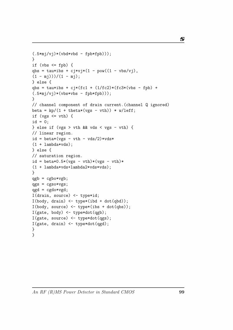
(.5*mj/vj)*(vbd*vbd - fpb*fpb)));
if (vbs <= fpb)
qbs = tau*ibs + cj*vj*(1 - pow((1 - vbs/vj),
(1 - mj)))/(1 - mj);
else
qbs = tau*ibs + cj*(fc1 + (1/fc2)*(fc3*(vbs - fpb) +
(.5*mj/vj)*(vbs*vbs - fpb*fpb)));
// channel component of drain current.(channel Q ignored)
beta = kp/(1 + theta*(vgs - vth)) * w/leff;
if (vgs <= vth)
id = 0;
else if (vgs > vth && vds < vgs - vth)
// linear region.
id = beta*(vgs - vth - vds/2)*vds*
(1 + lambda*vds);
else
// saturation region.
id = beta*0.5*(vgs - vth)*(vgs - vth)*
(1 + lambda*vds+lambda2*vds*vds);
qgb = cgbo*vgb;
qgs = cgso*vgs;
qgd = cgdo*vgd;
I(drain, source) <- type*id;
I(body, drain) <- type*(ibd + dot(qbd));
I(body, source) <- type*(ibs + dot(qbs));
I(gate, body) <- type*dot(qgb);
I(gate, source) <- type*dot(qgs);
I(gate, drain) <- type*dot(qgd);
An RF (R)MS Power Detector in Standard CMOS 99

APPENDIX C. BASIC LEVEL 1 MOS MODEL (SPECTREHDL)
100 Master Thesis

Appendix D
Final Kimura (MT)-basedcircuit
Figure D.1 shows the schematic of the Kimura (MT)-based circuit, whichcontains two Kimura (MT) squaring cells and a feedback loop.
The averaging circuit is realized with a resistor and a parallel capacitorwith a time constant of
τ = 10 MΩ · 250 fF = 2.5 µs (D.1)
These values are optimized by simulations with a sine wave input. So, it ispossible that this averaging circuit is not the best for a very complex signal,e.g. CDMA.
101

APPENDIX D. FINAL KIMURA (MT)-BASED CIRCUIT
Figure D.1: Kimura (MT) circuit.
102 Master Thesis

Appendix E
Bipolar squaring cells
This section shows some examples of published bipolar squaring cells. Thesquaring cells in section 4.4.3 can be implemented as a simple transconduc-tance cell and are discussed in this chapter.
Squaring cells doubles the dynamic range of an input signal. So the squar-ing cells and the averaging circuit must be very well-balanced to maintaina high accuracy for small inputs [54]. To provide a good balanced squaringcell, some transistors should be laid out (parallel) on the chip in a cross-quadconnection to cancel the effects of thermal and doping gradients [22]. Thehigh degree of balance between both squaring cells is provided by carefuldesign, e.g. a single bias voltage, as well as the physical structure, like devicematching and layout techniques [54].
The zero-signal current1 from a squaring cell should be as small as possiblefor the following reasons; When using one squaring cell, the output signalcan be better discerned from this current; When using two squaring cells,a high zero-signal current intensifies device mismatches and jeopardizes thebalance between both cells [25].
The next squaring cells of figures E.1, E.2 and E.3 show the designs withbipolar transistors, but they could also be realized with other polarities anddevice types (including MOSFETs) [23, 26, 54]. So when utilizing otherdevices with fairly minor changes to the designs, these squaring cells aresuitable for a lot of applications.
E.1 Triplet multi-tanh squaring cell
Accurate square law approximation from DC up to microwave frequencies canbe achieved by implementing the squaring cells as balanced series-connected
1Sometimes indicated with quiescent current or standing current.
103

APPENDIX E. BIPOLAR SQUARING CELLS
three-transistor common-emitter multi-tanh transconductance cells as shownin figure E.1. Some of the implicit approximation errors are essentially can-celled by using carefully balanced squaring cells [22].
e
Q1
RB
Q2
Q3
RB
IT
Ae e
iOUT
vIN+
vIN-
Figure E.1: Squaring cell implemented as a series-connected three-transistorcommon-emitter multi-tanh transconductance cell.
The tail current IT is realized by a bias circuit. The differential inputvoltage is connected to the two outside transistors. Both resistors RB resultin the voltage drive to this two transistors being balanced in amplitude. Themiddle transistor has an emitter area of ‘Ae’ and is ‘A’ times larger than theouter transistors. These outer transistors provide current iOUT to an erroramplifier. For small values of |x| (< 3) and using dual squaring cells forcancelling the offset value, this current can be approximated by [22]
iOUT =x2
4(1 + A−1) + AIT (E.1)
where
x =vIN
2vT=
qvIN
2kT(E.2)
It has been determined that A = 26 provides a very good approximation to asquare law form over an acceptable range of input voltage. See [22] for moredetails.
When the tail current of figure E.1 is dependent on the control signalinstead of a fixed bias current, the squaring cell is suitable for use as a scalingsquaring cell [23]. The temperature independency of this squaring cell canbe increased when utilizing two overlapping (parallel) squaring cells drivenby different tail currents with unequal temperature characteristics. See [23]for more details.
104 Master Thesis

E.2. LOW SUPPLY CURRENT SQUARING CELL
E.2 Low supply current squaring cell
Another circuit for a squaring cell is shown in figure E.2. The squaring cellis implemented as a common-base transistor with a two-transistor currentmirror and is based on the translinear principle. The circuit provides veryhigh input frequencies and low power supply currents.
Q1
iOUT
VBIAS
Q3
iIN
Q2
Q5
Q4
IBIAS
Figure E.2: Squaring cell implemented with a common-base transistor and acurrent mirror.
The upper transistor Q1 has a common-base, which means that the baseis connected to an AC ground. The lower two transistors, Q2 and Q3, forms acurrent mirror. The input signal is connected to the emitter of the common-base transistor and the input of the current mirror (Q2). The output currentis provided by the collector of the common-base transistor and the output ofthe current mirror (Q3). DC input currents should be eliminated by a block-ing capacitor. The squaring cell is biased by two series-connected transistors,Q4 and Q5. Both transistors are diode-connected in series between the biascurrent IBIAS and ground to provide the bias voltage.
The resulting quiescent currents in the first three transistors are propor-tional to absolute temperature (PTAT), so that the input impedance remainsconstant with temperature. The input impedance can be adjusted by the biascurrent. All transistors have the same emitter areas.
For input currents that have a small amplitude compared to the biascurrent (iIN ≪ 4IBIAS) and using dual squaring cells for cancelling the offsetvalue, the output current can be approximated by the squaring function [54]
iOUT ≈ i2IN4IBIAS
(E.3)
For input currents that have a large amplitude compared to the bias current(iIN ≫ 4IBIAS), the output current can be approximated by the absolute-
An RF (R)MS Power Detector in Standard CMOS 105

APPENDIX E. BIPOLAR SQUARING CELLS
value function [54]iOUT ≈ |iIN| (E.4)
The accuracy can be improved by adding components as transistors, re-sistors and capacitors. The power consumption of the circuit can be reducedby using a smaller bias current and reducing the emitter areas of transistorsQ4 and Q5 with respect to the other ones. The input voltage range can beincreased by using emitter resistors in series with the first three transistors.See [54] for more details.
E.3 Squaring/weighting cell
A suitable squaring cell for figure 4.15 is shown in figure E.3. Figure E.3 in-cludes two exponential current generators which are separated with a dottedline. Both includes two emitter followers and generate output currents iC1
and iC2, which vary exponentially in response to the differential input volt-age [26]. When assuming that both current generators have equal emitter
Q1
iC1
Q3
iOUT
Q4
IBIAS
RE
vIN
Q2
Q7
iC2
Q5
Q8
IBIAS
RE
Q6
vIN+
vIN-
Figure E.3: More details of a suitable squaring cell for figure 4.15.
areas, neglecting the effect of RE and quiescent offset value, the total outputcurrent is [26]
iOUT = IBIAS
(e
vIN2vT + e
−vIN2vT
)(E.5)
≈ IBIAS
(
2 +
(vIN
2vT
)2
+1
12
(vIN
2vT
)4
· · ·)
(E.6)
106 Master Thesis

E.3. SQUARING/WEIGHTING CELL
and finally is dominated by the square term. When including the degenera-tion resistors RE, the effect of the fourth and higher order terms in the seriesexpansion of equation (E.6) diminishes.
The minimum bias current, and thus the zero-signal current, is limitedby the fact that RE cannot be made too large, because then the outputwill become very linear in response to large input signals and the squarelaw behavior is lost. This problem can be overcome by adding collectorresistors RC in series with the collectors of transistors Q2 and Q6 as shownin figure E.4. The voltage drop across these resistors is independent of theinput signal. So the zero-signal current can be reduced without significantlycompromising the response to large input signals. The voltage drop acrossRC should not made too large, because then the accuracy to small inputsignals is decreasing. The optimum value is usually approx a few times thethermal voltage VT [25].
Q2
(1)
(2)
(3)
Q2
RC
(1)
(2)
(3)
Figure E.4: Adding collector resistors to reduce zero-signal current.
The bias currents and the input voltage should be made PTAT to compen-sate for temperature variations. The weighting function can be implementedwith dependent bias currents in response to the weighting signal αn. See [26]for more details.
An RF (R)MS Power Detector in Standard CMOS 107

APPENDIX E. BIPOLAR SQUARING CELLS
108 Master Thesis
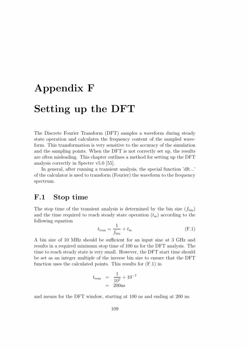
Appendix F
Setting up the DFT
The Discrete Fourier Transform (DFT) samples a waveform during steadystate operation and calculates the frequency content of the sampled wave-form. This transformation is very sensitive to the accuracy of the simulationand the sampling points. When the DFT is not correctly set up, the resultsare often misleading. This chapter outlines a method for setting up the DFTanalysis correctly in Spectre v5.0 [55].
In general, after running a transient analysis, the special function ’dft...’of the calculator is used to transform (Fourier) the waveform to the frequencyspectrum.
F.1 Stop time
The stop time of the transient analysis is determined by the bin size (fbin)and the time required to reach steady state operation (tss) according to thefollowing equation
ttran =1
fbin+ tss (F.1)
A bin size of 10 MHz should be sufficient for an input sine at 3 GHz andresults in a required minimum stop time of 100 ns for the DFT analysis. Thetime to reach steady state is very small. However, the DFT start time shouldbe set as an integer multiple of the inverse bin size to ensure that the DFTfunction uses the calculated points. This results for (F.1) in
ttran =1
107+ 10−7
= 200ns
and means for the DFT window, starting at 100 ns and ending at 200 ns.
109
APPENDIX F. SETTING UP THE DFT
F.2 Number of samples
The minimum number of sample points required by the DFT is determined bythe maximum frequency of the spectrum. The highest frequency of interestfor this study is the sixth order of the input signal. The input signal is setto 3 GHz and then the sixth order is at 18 GHz. The spectrum around thismaximum frequency is also of interest, therefore the maximum frequency willbe rounded up to 20 GHz. The minimum number of samples to obtain thisfrequency information from the waveform, is
Nsamples,min = fmax ·2
fbin(F.2)
= 20 · 109 · 2
107
= 4000
The number of sample points is chosen larger than this minimum, becausethey are often specified as a power of two.
Nsamples = 2⌈2log Nsamples,min⌉ (F.3)
= 4096
F.3 Accuracy
During a simulation, Cadence selects points to calculate and interpolatesbetween them to create the output waveform. The points are based on therate of change of the signal(s). The interpolation results for the DFT inapproximations and loss of accuracy. When the DFT function will sample theexact points, which the simulator has calculated, the accuracy is maintained.This is possible with strobing, which lets you select the time interval betweenthe data points that the simulator saves [56]. You can compare it with astrobe light at a rotating unit. The simulator can be forced to calculatethese fixed points by defining the ‘strobeperiod’ parameter, which can befound via
Analyses → Choose... (check tran)1 → Options... → OUTPUT
PARAMETERS
In this field, enter the equation
1
fbin · Nsamples
=1
107 · 4096(F.4)
1The options ‘conservative’, ‘moderate’ and ‘liberal’ should not be checked here.
110 Master Thesis

F.3. ACCURACY
The accuracy is also decreased when entering a rounded number instead ofthis equation.
The accuracy can also be increased by changing the tolerances, which canbe found via
Simulation → Options → Analog... → TOLERANCE OPTIONS
These options determine resolution and accuracy for the simulation. Smallertolerances means the simulation needs more memory and takes more time tosimulate. The default values
reltol = 10−3
vabstol = 10−6
iabstol = 10−12
are slightly too loose for accurate analysis. For the simulations in this studyare used more tighten tolerances, as
reltol = 10−8
vabstol = 10−11
iabstol = 10−17
With these tolerances, the time taken to simulate is still smaller than halvea minute. This difference of five decades is determined as a result of severalsimulations and is a good trade off between the time to simulate and theaccuracy. The ‘reltol’ parameter sets the maximum relative tolerance forvalues calculated in the last two iterations [56]. The ‘vabstol’ and ‘iabstol’parameters set absolute tolerances for differences in the calculated values ofvoltages and currents in the last two iterations [56]. So, ‘reltol’ mainly con-trols the accuracy and is responsible for the time, which is taken to simulate.This time is doubled approximately for every decreased decade of ‘reltol’.
An RF (R)MS Power Detector in Standard CMOS 111

APPENDIX F. SETTING UP THE DFT
112 Master Thesis

Appendix G
Setting up the PSS
The Periodic Steady-State (PSS) analysis calculates the PSS response of acircuit at a specified fundamental frequency, with a simulation time indepen-dent of the time-constants of the circuit. This chapter outlines a method forsetting up the PSS analysis correctly in Spectre v5.0.
G.1 Accuracy
The accuracy of the PSS analysis must be adjusted and can be found via
Analyses → Choose ... (check pss) → Accuracy Defaults (errp-reset)
For the highest accuracy (extremely low noise floor), the ‘conservative’ optionshould be checked.
For a still higher accuracy, it is also possible to change the tolerances asdescribed in F.3.
G.2 Stabilization time
An easy way to define the time when the PSS begins, is by adjusting thestabilization time parameter (tstab), which can be found via
Analyses → Choose ... (check pss) → Additional Time for Sta-bilization (tstab)
For the circuits in chapter 6, 10 ns (30 periods) is used.
113
APPENDIX G. SETTING UP THE PSS
G.3 Frequency spectrum
In general, after running a PSS analysis, the frequency spectrum can beshown via
Results → Direct Plot → Main Form ...
For plotting the spectrum of a (differential) current, the next adjustmentsare required
Outputs → Save All ... → Select device currents (currents): allOutputs → Save All ... → Select AC terminal currents (useprobes):yes
The maximum frequency of the spectrum is determined by the ‘numberof harmonics’ times the ‘beat frequency’. These settings can be found via
Analyses → Choose ... (check pss) → Beat FrequencyAnalyses → Choose ... (check pss) → Output harmonics → Num-ber of harmonics
The number of frequencies can be increased (smaller steps) by decreasing the‘beat frequency’ and increasing the ‘number of harmonics’.
The highest frequency of interest for this study is the sixth order of theinput signal. The input signal is set to 3 GHz and then the sixth order isat 18 GHz. The input frequency must be an integer multiple of the ‘beatfrequency’. So, the maximum ‘beat frequency’ is 3 GHz, which results in 6harmonics.
114 Master Thesis

Acknowledgements
The project was a cooperation between National Semiconductor in Delft andthe University of Twente in Enschede. The assignment is considered byNational, but is carried out at the Integrated Circuit Design group of theUniversity. During this project, I have learned a lot about IC design andI gained a lot of new insights. I enjoyed working on the assignment and Ifound it a real challenge.
I would like to use this opportunity to thank some persons particularly.First of all, I would like to thank National Semiconductor for giving methe opportunity to work on this assignment. Especially, I would like tothank my (daily) supervisor, Anne-Johan Annema, for his enormous support,guidance and help with valuable discussions and suggestions during the wholeassignment. Without his help it had been much more difficult. Also specialthanks goes to Rudy Eschauzier and Michiel Kouwenhoven from NationalSemiconductor and Bram Nauta from the UT for their guidance, supportand valuable advise. Working with Cadence and Unix was not easy but Igot help from some real experts. So I like to thank Gerard Wienk of theUT for his support using the Cadence environment and Frederik Reendersfor his computer support. I am also thankful to Gerdien Lammers of thesecretary for all administrative activities. All proceedings for the assignmentare performed at the University of Twente Enschede, therefore I would liketo thank all employees and students on the third floor of the ’Hogekamp’building for their hospitality and pleasant environment. Finally, to everyonewho is not mentioned above and has made this project possible and a pleasantexperience, thank you very much.
Frank van der AaUniversity of Twente, EnschedeJuly 18, 2006
115

APPENDIX G. ACKNOWLEDGEMENTS
116 Master Thesis

Bibliography
[1] J. F. White, High Frequency Techniques: An Introduction to RF andMicrowave Engineering. John Wiley & Sons, Inc., usa ed., 2004.
[2] J. C. Cowles, “The Evolution of Integrated RF Power Measurement andControl,” Proceedings of the 12th IEEE Mediterranean ElectrotechnicalConference (MELECON), vol. 1, pp. 131–134, May 2004.
[3] National Semiconductor, www.national.com, LMV243 Single-Channel,Quad-Band GSM Power Controller in micro SMD, February 2004.
[4] M. H. L. Kouwenhoven, “3G Mobile Wireless Communication Systems:An Overview Focusing on Requirements and Trends for TransmitterPower Control Hardware,” (Confidential report) Revision 1.1, NationalSemiconductor, November 2005.
[5] E. Nash, “High-Speed Logamps Precisely Detect Power,” Microwaves &RF, vol. 43, September 2004.
[6] C. Kitchen and L. Counts, RMS-to-DC Conversion Application Guide.Analog Devices, Inc., second ed., 1986.
[7] A. Kryshtopin, R. Kravchenko, A. Chernyakov, K. Markov, G. Sevskiy,T. Kerssenbrock, and P. Heide, “Novel High-Accuracy LTCC-IntegratedPower Monitors for 2.4 and 5 GHz Wireless-LAN Applications,” IEEEMTT-S International Microwave Symposium Digest, vol. 2, pp. 1277–1280, June 2004.
[8] E. L. Firrao, A. J. Annema, and B. Nauta, “Antenna Behaviour in thePresence of Human Body,” Proceedings ProRISC, pp. 487–490, 2004.
[9] E. Nash, “Logarithmic amplifiers explained,” Ask the ApplicationsEngineer—28, vol. 33, no. 3, 1999.
117

BIBLIOGRAPHY
[10] E. Nash, AN-653 Improving Temperature, Stability and Linearity of HighDynamic Range RMS RF Power Detectors, Rev. 0. Analog Devices,www.analog.com, 2003.
[11] W. M. Leach, “Fundamentals of Low-Noise Analog Circuit Design,”Proceedings of the IEEE, vol. 82, pp. 1515–1538, October 1994.
[12] H. Pretl, L. Maurer, W. Schelmbauer, R. Weigel, B. Adler, and J. Fenk,“Linearity considerations of W-CDMA front-ends for UMTS,” IEEEMTT-S International Microwave Symposium Digest, vol. 1, pp. 433–436, June 2000.
[13] J. Vankka, M. Honkanen, and K. A. I. Halonen, “A MulticarrierGMSK Modulator,” IEEE Journal on Selected Areas in Communica-tions, vol. 19, pp. 1070–1079, June 2001.
[14] P. Genest, H. Grandry, and H. Chaoui, “Criteria for Selecting RF PowerDetectors,” High Frequency Electronics, vol. 3, pp. 52–55, June 2004.
[15] T. Zhang and R. M. F. William R. Eisenstadt, “A Novel 5GHz RFPower Detector,” Proceedings of the IEEE International Symposium onCircuits and Systems (ISCAS), vol. 1, pp. 897–900, May 2004.
[16] M. Ratni, B. Huyart, E. Bergeault, and L. Jallet, “RF Power Detec-tor Using a Silicon MOSFET,” IEEE MTT-S International MicrowaveSymposium Digest, vol. 2, pp. 1139–1142, June 1998.
[17] R. G. Meyer, “Low-Power Monolithic RF Peak Detector Analysis,”IEEE Journal of Solid-State Circuits, vol. 30, pp. 65–67, January 1995.
[18] S. Kulhalli, S. Seth, and S.-T. Fu, “An Integrated Linear RF Power De-tector,” Proceedings of the IEEE International Symposium on Circuitsand Systems (ISCAS), vol. 1, pp. 625–628, May 2004.
[19] S. Ho, “A 450 MHz CMOS RF Power Detector,” IEEE Radio FrequencyIntegrated Circuits (RFIC) Symposium. Digest of Papers., pp. 209–212,May 2001.
[20] G. Klahn, “True RMS Power Detection with High Dynamic Range,”IEEE MTT-S International Microwave Symposium Digest, vol. 4,pp. 1773–1776, June 1999.
[21] J. G. Petrofsky, “Apparatus and Methods for Performing RMS-to-DCConversion with Bipolar Input Signal Range,” United States Patent US6,359,576 B1, Linear Technology, March 2002.
118 Master Thesis

BIBLIOGRAPHY
[22] B. Gilbert, “RMS-to-DC Converter with Balanced Multi-tanh TripletSquaring Cells,” United States Patent US 6,204,719 B1, Analog Devices,March 2001.
[23] B. Gilbert, “RMS-DC Converter Having Detector Cell with Dynami-cally Adjustable Scaling Factor,” United States Patent US 6,348,829B1, Analog Devices, February 2002.
[24] Analog Devices, www.analog.com, AD8361 LF to 2.5 GHz TruPwrTM
Detector, Rev. C, August 2004.
[25] B. Gilbert, “RMS-DC Converter Using a Variable Gain Amplifier toDrive a Squaring Cell,” United States Patent US 6,429,720 B1, AnalogDevices, August 2002.
[26] B. Gilbert, “RMS-DC Converter Having Gain Stages with VariableWeighting Coefficients,” United States Patent US 6,437,630 B1, Ana-log Devices, August 2002.
[27] Analog Devices, www.analog.com, AD8313 0.1 GHz to 2.5 GHz 70 dBLogarithmic Detector/Controller, Rev. D, June 2004.
[28] Analog Devices, www.analog.com, AD8362 50 Hz to 2.7 GHz 60 dBTruPwrTM Detector, Rev. C, September 2005.
[29] Analog Devices, www.analog.com, ADL5500 100 MHz to 6 GHzTruPwrTM Detector, Rev. 0, July 2005.
[30] National Semiconductor, www.national.com, LMV232 Dual-Channel In-tegrated Mean Square Power Detector for CDMA & WCDMA, April2005.
[31] B. Gilbert and L. W. Counts, “A Monolithic RMS-DC Converter withCrest-Factor Compensation,” IEEE International Solid-State CircuitsConference (ISSCC), vol. XIX, pp. 110–111, February 1976.
[32] E. Seevinck, R. F. Wassenaar, and H. C. K. Wong, “A Wide-Band Tech-nique for Vector Summation and RMSDC Conversion,” IEEE Journalof Solid-State Circuits, vol. 19, pp. 311–318, June 1984.
[33] K. Bult and H. Wallinga, “A Class of Analog CMOS Circuits Basedon the Square-Law Characteristic of an MOS Transistor in Saturation,”IEEE Journal of Solid-State Circuits, vol. 22, pp. 357–365, June 1987.
An RF (R)MS Power Detector in Standard CMOS 119

BIBLIOGRAPHY
[34] R. F. Wassenaar, E. Seevinck, M. G. van Leeuwen, C. J. Speelman, andE. Holle, “New Techniques for High-Frequency RMS-to-DC ConversionBased on a Multifunctional V-to-I Convertor,” IEEE Journal of Solid-State Circuits, vol. 23, pp. 802–815, June 1988.
[35] R. J. Wiegerink, Analysis and Synthesis of MOS Translinear Circuits.PhD thesis, University of Twente, Enschede, October 1992.
[36] S.-I. Liu and D.-J. Wei, “Analogue Squarer and Multiplier Based onMOS Square-Law Characteristic,” IEEE Electronics Letters, vol. 32,pp. 541–542, March 1996.
[37] J. Mulder, A. C. van der Woerd, W. A. Serdijn, and A. H. M. vanRoermund, “An RMS-DC Converter Based on the Dynamic TranslinearPrinciple,” IEEE Journal of Solid-State Circuits, vol. 32, pp. 1146–1150,July 1997.
[38] W. Surakampontorn and K. Kumwachara, “A Dual Translinear-BasedTrue RMS-to-DC Converter,” IEEE Transactions on Instrumentationand Measurement, vol. 47, pp. 459–464, April 1998.
[39] A. J. Lopez-Martin and A. Carlosena, “A Tunable CMOS Square-RootDomain Oscillator,” Proceedings of the IEEE International Symposiumon Circuits and Systems (ISCAS), vol. 5, pp. 573–576, May 2000.
[40] A. J. Lopez-Martin and A. Carlosena, “A 1.5 V CMOS Square-RootDomain Filter,” The 8th IEEE International Conference on Electronics,Circuits and Systems (ICECS), vol. 3, pp. 1465–1468, September 2001.
[41] A. J. Lopez-Martin and A. Carlosena, “A Current-Mode CMOS RMS-DC Converter for Very Low-Voltage Applications,” The 8th IEEE In-ternational Conference on Electronics, Circuits and Systems (ICECS),vol. 1, pp. 425–428, September 2001.
[42] K. Kaewdang, K. Kumwachara, and W. Surakampontorn, “A Real-ization of Simple Current-Mode CMOS Based True RMS-to-DC Con-verter,” Proceedings of the IEEE Asia-Pacific Conference on Circuitsand Systems, vol. 2, pp. 733–736, December 2004.
[43] S. Wisetphanichkij, N. Singkrajom, M. Kumngern, and K. Dejhan, “ALow-Voltage CMOS Current Squarer Circuit,” IEEE International Sym-posium on Communications and Information Technology (ISCIT), vol. 1,pp. 271–274, October 2005.
120 Master Thesis

BIBLIOGRAPHY
[44] A. Nedungadi and T. Viswanathan, “Design of Linear CMOS Transcon-ductance Elements,” IEEE Transactions on Circuits and Systems,vol. 31, pp. 891–894, October 1984.
[45] H.-J. Song and C.-K. Kim, “An MOS Four-Quadrant Analog Multi-plier Using Simple Two-Input Squaring Circuits with Source Followers,”IEEE Journal of Solid-State Circuits, vol. 25, pp. 841–848, June 1990.
[46] S.-I. Liu and Y.-S. Hwang, “CMOS Squarer and Four-Quadrant Mul-tiplier,” IEEE Transactions on Circuits and Systems I: FundamentalTheory and Applications, vol. 42, pp. 119–122, February 1995.
[47] K. Kimura, “Some Circuit Design Techniques for Low-Voltage AnalogFunctional Elements Using Squaring Circuits,” IEEE Transactions onCircuits and Systems I: Fundamental Theory and Applications, vol. 43,pp. 559–576, July 1996.
[48] G. Han and E. Sanchez-Sinencio, “CMOS Transconductance Multipliers:A Tutorial,” IEEE Transactions on Circuits and Systems II: Analog andDigital Signal Processing, vol. 45, pp. 1550–1563, December 1998.
[49] E. Seevinck and R. F. Wassenaar, “A Versatile CMOS LinearTransconductor/Square-Law Function Circuit,” IEEE Journal of Solid-State Circuits, vol. 22, pp. 366–377, June 1987.
[50] M. Panovic and A. Demosthenous, “Compact CMOS Linear Transcon-ductor and Four-quadrant Analogue Multiplier,” Proceedings of theIEEE International Symposium on Circuits and Systems (ISCAS),vol. 1, pp. I – 685–688, May 2004.
[51] C. A. D. L. Cruz-Blas, A. J. Lopez-Martin, and A. Carlosena, “1.5 VTunable Square-Root Domain filter,” IEEE Electronics Letters, vol. 40,pp. 213–214, February 2004.
[52] C. A. D. L. Cruz-Blas, A. Lpez-Martn, A. Carlosena, and J. Ramrez-Angulo, “1.5-V Current-Mode CMOS True RMSDC Converter Basedon Class-AB Transconductors,” IEEE Transactions on Circuits and Sys-tems II: Analog and Digital Signal Processing, vol. 52, pp. 376–379, July2005.
[53] B. Razavi, Design of Analog CMOS Integrated Circuits. Electrical andComputer Engineering, McGraw-Hill, international ed., 2001.
An RF (R)MS Power Detector in Standard CMOS 121

BIBLIOGRAPHY
[54] B. Gilbert, “Low Supply Current RMS-to-DC Converter,” United StatesPatent US 6,172,549 B1, Analog Devices, January 2001.
[55] J. Abbott, “Phase Detector and Charge Pump Design – 1.1 Setting upthe DFT,” tech. rep., RFIC 5503 Assignment 1, March 2004.
[56] Cadence, Spectrer Circuit Simulator User Guide, Product Version 5.0,January 2004.
122 Master Thesis