an rf lc q-enhanced cmos lter using integrated inductors ... · requirement for o -chip passive...
TRANSCRIPT

Pedro Daniel Manta de Almeida
Licenciado em Ciencias da Engenharia Electrotecnica e de
Computadores
An RF LC Q-enhanced CMOS filter using
Integrated Inductors with layout
optimization
Dissertacao apresentada para obtencao do Grau de Mestre em
Engenharia Electrotecnica e de Computadores, pela Universidade Nova
de Lisboa, Faculdade de Ciencias e Tecnologia.
Orientador : Maria Helena Silva Fino, FCT-UNL
Juri:
Presidente: Prof. Fernando Jose Vieira do Coito
Arguentes: Prof. Luis Bica de Oliveira
Vogais: Prof. Maria Helena Silva Fino
Prof.
Abril, 2013

i
RF LC Q-enhanced CMOS filter using Integrated Inductors with layout opti-
mization
Copyright © Pedro Daniel Manta de Almeida, Faculdade de Ciencias e Tecnologia, Uni-
versidade Nova de Lisboa
A Faculdade de Ciencias e Tecnologia e a Universidade Nova de Lisboa tem o direito,
perpetuo e sem limites geograficos, de arquivar e publicar esta dissertacao atraves de ex-
emplares impressos reproduzidos em papel ou de forma digital, ou por qualquer outro meio
conhecido ou que venha a ser inventado, e de a divulgar atraves de repositorios cientıficos
e de admitir a sua copia e distribuicao com objectivos educacionais ou de investigacao,
nao comerciais, desde que seja dado credito ao autor e editor.

ii

To my parents and my girlfriend
iii

iv
Acknowledgements
I am deeply grateful to my advisor Prof. Helena Fino for her expert guidance, stimu-
lating suggestions, patience, constant encouragement and never-ending supports.
I must to thank all my colleagues and friends that I have interacted with in the past few
years. They exposed me to a variety of challenging, invigorating and enjoyable experiences.
I want to give a special thanks to a very important person in my life, Carlota Faria,
for the encouragement and motivation in the long journey of my research and for helping
me stay focused and stabilized.
Finally, a special thanks to my parents, Isabel e Daniel Almeida, for their love and
support. My parents have always believed in and encouraged me in all my endeavors and
without their support I would never have been able to accomplish what I have now.
You all deserve the best.
v

vi

Abstract
The advancement of CMOS technology led to the integration of more complex func-
tions in a single chip. In the particular of wireless transceivers, integrated LC tanks are
becoming popular both for VCOs and integrated filters. The design of a 2nd order CMOS
0.13 µm Q-enhanced integrated LC filter for a frequency of 2.44 GHz is presented. The
intent of this filter is to create a circuit for integrated wireless receiver and minimize the
requirement for off-chip passive filter components, reducing the overall component count
and size of wireless devices and systems. For RF applications the main challenge is still
the design of integrated inductors with the maximum quality factor. For that purpose,
tapered, i.e, variable width inductors have been introduced in the literature. In this work,
a characterization of variable width integrated inductors is proposed. This inductor model
is then integrated into an optimization procedure where inductors with a quality factor
improvement are obtained.
Keywords: Inductor layout optimization, variable metal width, integrated RF
inductor, Q-enhanced RF LC filter.
vii

viii

Resumo
Com o avanco da tecnologia CMOS surgiram funcionalidades mais complexas num
unico circuito integrado. No caso particular de emissores-receptores sem fios, tanques
integrados LC estao a tornar-se populares, tanto para VCOs (Osciladores controlados por
tensao) como para filtros integrados. O projecto de um filtro LC integrado de segunda
ordem com melhoramento de factor de qualidade e apresentado neste trabalho. A intencao
deste filtro e a de criar um circuito integrado para a recepcao sem fios minimizando o
requisito de componentes passivos nao integrados, reduzindo o numero de componentes e
tamanho global de dispositivos sem fios e sistemas. Para aplicacoes de RF (Frequencia de
radio) o principal desafio ainda e o projecto de bobines integradas com elevado factor de
qualidade. Para este efeito, bobines de espessura variavel tem sido propostas por varios
autores. Nesta tese e proposta uma caracterizacao de bobines integradas de espessura
variavel. Este modelo de bobine e entao integrado num processo de optimizacao, onde sao
obtidas bobines com uma melhoria de factor de qualidade
Palavras Chave:Optimizacao geometrica da bobibe, espessura variavel, bobine
integrada, Filtro LC com melhoramento do factor de qualidade
ix

x

Contents
Acknowledgements v
Abstract vii
Sumario ix
1 Introduction 1
2 Integrated inductors 5
2.1 Introduction . . . . . . . . . . . . . . . . . . . . . . . . . . . . . . . . . . . . 5
2.2 Inductor model . . . . . . . . . . . . . . . . . . . . . . . . . . . . . . . . . . 6
2.2.1 Metal length . . . . . . . . . . . . . . . . . . . . . . . . . . . . . . . 8
2.2.2 Series Inductance . . . . . . . . . . . . . . . . . . . . . . . . . . . . . 9
2.2.3 Series Resistance . . . . . . . . . . . . . . . . . . . . . . . . . . . . . 10
2.2.4 Crossover Capacitance . . . . . . . . . . . . . . . . . . . . . . . . . . 11
2.2.5 Oxide Capacitance . . . . . . . . . . . . . . . . . . . . . . . . . . . . 11
2.2.6 Substrate Resistance and Capacitance . . . . . . . . . . . . . . . . . 12
2.3 Quality Factor of an Inductor . . . . . . . . . . . . . . . . . . . . . . . . . . 12
2.4 Working Examples . . . . . . . . . . . . . . . . . . . . . . . . . . . . . . . . 15
2.4.1 Conclusion . . . . . . . . . . . . . . . . . . . . . . . . . . . . . . . . 17
3 Integrated inductors with variable width 19
3.1 Introduction . . . . . . . . . . . . . . . . . . . . . . . . . . . . . . . . . . . . 19
3.2 Variable width inductors . . . . . . . . . . . . . . . . . . . . . . . . . . . . . 20
3.2.1 Modeling variable inductors . . . . . . . . . . . . . . . . . . . . . . . 23
3.3 Validation of the model . . . . . . . . . . . . . . . . . . . . . . . . . . . . . 26
3.4 Optimization . . . . . . . . . . . . . . . . . . . . . . . . . . . . . . . . . . . 27
3.4.1 Example 1 . . . . . . . . . . . . . . . . . . . . . . . . . . . . . . . . . 28
3.4.2 Example 2 . . . . . . . . . . . . . . . . . . . . . . . . . . . . . . . . . 28
3.4.3 Conclusion . . . . . . . . . . . . . . . . . . . . . . . . . . . . . . . . 29
4 An RF LC Q-Enhanced CMOS filter 31
4.1 Introduction . . . . . . . . . . . . . . . . . . . . . . . . . . . . . . . . . . . . 31
xi

xii CONTENTS
4.2 Tuned Amplifiers . . . . . . . . . . . . . . . . . . . . . . . . . . . . . . . . . 32
4.3 Principles of Q enhancement . . . . . . . . . . . . . . . . . . . . . . . . . . 34
4.4 Integrated Filters design . . . . . . . . . . . . . . . . . . . . . . . . . . . . . 39
4.4.1 Simulation results . . . . . . . . . . . . . . . . . . . . . . . . . . . . 42
4.4.2 gmLC filter with regular integrated inductor . . . . . . . . . . . . . . 42
4.4.3 gmLC filter with optimized integrated inductor . . . . . . . . . . . . 44
4.4.4 Conclusions . . . . . . . . . . . . . . . . . . . . . . . . . . . . . . . . 46
5 Conclusions 49
Bibliography 51
A Publications 55

List of Figures
1.1 Typical radio receiver [1] . . . . . . . . . . . . . . . . . . . . . . . . . . . . . 2
2.1 Typical layout of an integrated spiral inductor . . . . . . . . . . . . . . . . 6
2.2 Simple 1-port model . . . . . . . . . . . . . . . . . . . . . . . . . . . . . . . 7
2.3 On-chip implementation of a spiral inductor . . . . . . . . . . . . . . . . . . 7
2.4 π circuit equivalent model of a spiral inductor . . . . . . . . . . . . . . . . . 8
2.5 One port equivalent model of π model . . . . . . . . . . . . . . . . . . . . . 13
2.6 Frequency dependence of 2.6(a) inductance and 2.6(b) the quality factor of
spiral inductor . . . . . . . . . . . . . . . . . . . . . . . . . . . . . . . . . . 16
2.7 Frequency dependence of 2.7(a) inductance and 2.7(b) the quality factor of
spiral inductor . . . . . . . . . . . . . . . . . . . . . . . . . . . . . . . . . . 17
2.8 Frequency dependence of 2.8(a) inductance and 2.8(b) the quality factor of
spiral inductor . . . . . . . . . . . . . . . . . . . . . . . . . . . . . . . . . . 17
3.1 Variable width square inductor [2] . . . . . . . . . . . . . . . . . . . . . . . 21
3.2 A regular spiral inductor divided by segments . . . . . . . . . . . . . . . . . 22
3.3 A non-uniform width spiral inductor divided by segments . . . . . . . . . . 22
4.1 Frequency response of a tuned amplifier . . . . . . . . . . . . . . . . . . . . 32
4.2 The basic principle of tuned amplifier is illustrated using a MOSFET with
a tuned circuit load. Bias details are not shown. . . . . . . . . . . . . . . . 32
4.3 Active Q-enhancement using negative resistance . . . . . . . . . . . . . . . 34
4.4 Q-enhancement technique applied to a RLC filter . . . . . . . . . . . . . . . 35
4.5 Q-enhanced LC bandpass filter . . . . . . . . . . . . . . . . . . . . . . . . . 36
4.6 A 2nd Q-enhanced on-chip LC bandpass filter . . . . . . . . . . . . . . . . . 43
4.7 Frequency response of the RF LC Q-enhanced filter using a regular spiral
inductor . . . . . . . . . . . . . . . . . . . . . . . . . . . . . . . . . . . . . . 44
4.8 Frequency response of the RF LC Q-enhanced filter using an optimized
spiral inductor . . . . . . . . . . . . . . . . . . . . . . . . . . . . . . . . . . 45
4.9 Frequency response of the RF LC Q-enhanced filter using a regular spiral
inductor . . . . . . . . . . . . . . . . . . . . . . . . . . . . . . . . . . . . . . 47
xiii

xiv LIST OF FIGURES
4.10 Frequency response of the RF LC Q-enhanced filter using a regular spiral
inductor . . . . . . . . . . . . . . . . . . . . . . . . . . . . . . . . . . . . . . 47

List of Tables
2.1 Modified Wheeler Expression’s coefficients . . . . . . . . . . . . . . . . . . . 9
2.2 UMC130 - Technological Parameters . . . . . . . . . . . . . . . . . . . . . . 15
2.3 Spiral inductor design constraints . . . . . . . . . . . . . . . . . . . . . . . . 16
2.4 Results comparison with ASITIC - 710 MHz . . . . . . . . . . . . . . . . . . 16
3.1 Validity of the optimization model . . . . . . . . . . . . . . . . . . . . . . . 26
3.2 Results comparison with ASITIC . . . . . . . . . . . . . . . . . . . . . . . . 26
3.3 Validity of the optimization model . . . . . . . . . . . . . . . . . . . . . . . 26
3.4 Spiral inductor design constraints . . . . . . . . . . . . . . . . . . . . . . . . 27
3.5 UMC130 - Technological Parameters . . . . . . . . . . . . . . . . . . . . . . 27
3.6 Spiral inductor design constraints for inductance of 1nH . . . . . . . . . . . 28
3.7 Results comparison with ASITIC . . . . . . . . . . . . . . . . . . . . . . . . 28
3.8 Spiral inductor design constraints for inductance of 2 nH . . . . . . . . . . . 28
3.9 Results comparison with ASITIC . . . . . . . . . . . . . . . . . . . . . . . . 29
4.1 Inductor of 1 nH used in filter . . . . . . . . . . . . . . . . . . . . . . . . . . 40
4.2 Values of the Gneg and C . . . . . . . . . . . . . . . . . . . . . . . . . . . . 40
4.3 Value of the Width of the transistors MOS . . . . . . . . . . . . . . . . . . 41
4.4 Value of the Width of the transistors MOS (4,5,6) . . . . . . . . . . . . . . 42
4.5 Model π components values . . . . . . . . . . . . . . . . . . . . . . . . . . . 43
4.6 Simulation results . . . . . . . . . . . . . . . . . . . . . . . . . . . . . . . . 44
4.7 Model π components values . . . . . . . . . . . . . . . . . . . . . . . . . . . 45
4.8 Simulation results . . . . . . . . . . . . . . . . . . . . . . . . . . . . . . . . 45
4.9 Fine tuning resulting values . . . . . . . . . . . . . . . . . . . . . . . . . . . 46
4.10 Simulation results . . . . . . . . . . . . . . . . . . . . . . . . . . . . . . . . 47
xv

xvi LIST OF TABLES

Chapter 1
Introduction
The radio frequency (RF) and wireless market has suddenly expanded to unimaginable
dimensions. With the emergence of cellular phone, wireless local-area network (WLAN)
and Bluetooth technology, we are standing on the threshold of a new radio frequency
epoch. In the field of communication circuit design, the realization of the complete in-
tegration of RF transceivers and digital signal processing blocks onto a single integrated
circuit (IC) is a logical area in which to develop system-on-chip (SoC) solutions [3]-[4].
By doing this, the cost and the difficulty of assembly and tuning are reduced drastically.
Presently, the growing demand for multi-functional wireless communications systems is
becoming increasingly evident. Meanwhile, the lower cost and faster advance of CMOS
processes has motivated extensive efforts in designing RF CMOS circuits. CMOS tech-
nologies exhibit properties and limitations that directly impact the design of a receiver
from the architecture level to the device level and from the RF front end to the baseband
processor.
In the long term, traditionally analog functions of a radio receiver (see figure 1.1 will
be replaced with software or digital hardware. The final goal of a radio receiver would be
to digitalize the radio frequency (RF) signal at the out put of the antenna, allowing the
implementation of all receiver funtions in either digital hardware or software [5].
Achieving this would be very interesting for many reasons. It would reduce product
development time and costs. It would also allow to implement new functions that are
impossible to implement in analog hardware. Another great advantage would be the
1

2 CHAPTER 1. INTRODUCTION
possibility of creating receivers designed to allow reception of different modulation types.
Mixer
LOsine
Output
RFin RF BandSelect Filter RF Amp
IF BandpassFilter
ImageReject Filter IF Amp Demodulator
Figure 1.1: Typical radio receiver [1]
The ever increasing demand for wireless communications motivates in reducing com-
plexity, cost, power dissipation, and the number of external components in selecting re-
ceiver architecture (figure 1.1). The integrated inductors spiral plays an important role
in the development of Si RF ICs. The spiral inductor has a great influence on the per-
formance of many RF circuits. The obvious example is the LC tank, in which the quality
factor Q of the spiral inductor determines the bandwidth and the resonance impedance of
the LC tank. Another example is the bandpass filter built with inductor and capacitors, in
which the quality factor of the spiral inductor determines the insertion loss [6]. Following
the success in fabrication, intensive research has been conducted in the modeling of spiral
inductors on silicon. One approach is to use a compact circuit model. In other way, a
lot of work has been done in the synthesis and optimizations of spiral inductors in silicon.
The purpose of this thesis is to present an optimization method for the design of spiral
inductors. The focus for this optimization is on the geometric layout of the spiral induc-
tor. We develop a theory based on fundamental electronic principles that yields simple,
accurate inductance expression for on-chip spiral inductors of various geometries.
Besides the introduction, this thesis contains 4 chapters. In Chapter 2 an introduction
to integrated spiral inductors is presented, and the well known pi-model is introduced.
Analytical physics-based expressions for the model elements are givel, and finally working
examples proving the validity of the model are shown. In Chapter 3 the adequation of
the previously described model to variable width integrated indutors is described. After

3
validating this model, optimization methodologies are applied to the design of variable
width inductors, leading to final designs with quality factor improvement ( for the same
area) in the order of 20%. In Chapter 4 the variable with integrated inductors are used
for designing LC-filters. Examples considering the application for 2.44 GHz are presented.
Finally, in Chapter 5, conclusions are offered.

4 CHAPTER 1. INTRODUCTION

Chapter 2
Integrated inductors
The growth of wireless applications in the low GHz frequency range has been a catalyst
in numerous research activities to develop wireless applications. CMOS is considered a
technology of choice in the integration of radio frequency systems in the low frequency
range (up to a maximum of 10 GHz) because of the relatively lower costs in developing
single chip solutions over other semiconductor processes. For RFIC in CMOS, planar
inductors will have a dominant role in defining the achievable performance of the system
as a whole. Depending on the technology possibilities, several metal layers may be used
and different geometries can be adopted. In this work a 0.13µm CMOS technology is used
for implementing spiral inductors. In this chapter we review on-chip inductor realization
and see how they can be modeled.
2.1 Introduction
Inductors are components used to store energy in the form of magnetic field. However
integrated inductors are not easy to implement because of their non-ideal behaviour that
entail a myriad of trade-offs. Parasitic effects, such as coupling capacitance and losses
related to the integration substrate, affect these devices, degrading their performance [7].
In order to understand these trade-offs, both vertical and lateral of the layout have to be
considered.
Figure 2.1 shows a typical implementation of an integrated spiral inductor where the
important physical dimensions of the spiral inductor are identified: inner diameter (din),
5

6 CHAPTER 2. INTEGRATED INDUCTORS
Figure 2.1: Typical layout of an integrated spiral inductor
outer diameter (dout), space between turns (s) and width of metal trace (w). Since we
have chosen to fill in the spiral down to the inner diameter,
dout = din + 2nw + 2(n− 1)s (2.1)
.
The top and outermost end of the inductor are directly connected to a port while
the inner end is connected to the metal strip or air bridge from beneath. Generally, the
uppermost layer of metal is used for construction as it offers a low resistance to the current.
2.2 Inductor model
Quality factor (Q) of inductors in RFIC applications is poor. For achieving high
Q geometrical parameters of the inductors should be carefully determined so that the
highest Q for the given technology may be obtained. Since inductor design parameters
are highly correlated, optimization based design metodology are usually adopted. Since
electromagnetical simulation is a time consuming process, designers usually adopt inductor
models as a way of increasing the efficiency of the design task. Regarding integrated
inductor models the approach can be found accurate with literature.
While many simulation techniques focus on determining the complete network behav-
ior of an integrated inductor such as its 1- or 2-port s-parameters, this information is not
always in the most useful format for designers. The behavior of a device, such as the

2.2. INDUCTOR MODEL 7
inductors, may in fact be understood from the s-parameters, but designers are generally
interested in including one inductor device within a larger circuit or system. In this case,
it is necessary to have a more compact representation of the device for its inclusion in a
larger system. For this purpose, various models of integrated circuits represent compact
inductors have been developed [8].
The simplest model available for representing inductors, showed in figure 2.2, is useful
for characterizing the device’s behavior at low frequencies and is composed of an inductor
in series with a resistor that represents the ohmic losses along the length of the inductor.
L R
Figure 2.2: Simple 1-port model
This representation can be easily extracted directly from the 1-port complex impedance
of the device, Zin = R + jωL. However, at higher frequencies parasitic capacitors must
be taken into account and this model becomes insufficient.
In order to take into account the losses over a range of frequencies, circuits models of
spiral inductors on silicon, such as the simple π-model proposed in [9] and represented in
figures 2.3 and 2.4.
Figure 2.3: On-chip implementation of a spiral inductor
However and notwithstanding the fact that more accurate models have been proposed
and developed, the simple π-model of spiral inductor on silicon is the most common model
used by the designers due to its simplicity. Its parameters are easy to adjust to empirical
data and they have a clear physical meaning. As a trade-off, this is a narrow band model
because it is only valid for modeling the behavior of an inductor in a small range of
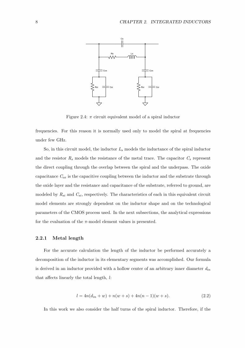
8 CHAPTER 2. INTEGRATED INDUCTORS
LsRs
Cs
Cox Cox
Rsi Csi Rsi Csi
Figure 2.4: π circuit equivalent model of a spiral inductor
frequencies. For this reason it is normally used only to model the spiral at frequencies
under few GHz.
So, in this circuit model, the inductor Ls models the inductance of the spiral inductor
and the resistor Rs models the resistance of the metal trace. The capacitor Cs represent
the direct coupling through the overlap between the spiral and the underpass. The oxide
capacitance Cox is the capacitive coupling between the inductor and the substrate through
the oxide layer and the resistance and capacitance of the substrate, referred to ground, are
modeled by Rsi and Csi, respectively. The characteristics of each in this equivalent circuit
model elements are strongly dependent on the inductor shape and on the technological
parameters of the CMOS process used. In the next subsections, the analytical expressions
for the evaluation of the π-model element values is presented.
2.2.1 Metal length
For the accurate calculation the length of the inductor be performed accurately a
decomposition of the inductor in its elementary segments was accomplished. Our formula
is derived in an inductor provided with a hollow center of an arbitrary inner diameter din
that affects linearly the total length, l :
l = 4n(din + w) + n(w + s) + 4n(n− 1)(w + s). (2.2)
In this work we also consider the half turns of the spiral inductor. Therefore, if the

2.2. INDUCTOR MODEL 9
spiral have an half turn it is necessary to add the length of that half turn,
length of half inductor = 2(din + w) + ni(w + s) (2.3)
where ni corresponds to the integer part of the number of turns.
2.2.2 Series Inductance
The knowledge of series inductance is a critical point to engineers who develop and
use on-chip inductors for RFICs. The inductance represents the magnetic energy stored
in the device, although parasitic components may store energy as well. For the evaluation
of the inductance, several approaches have been proposed, based either on fitting process
to experimental values [4] or through physics-based equations (modified Wheeler formula)
[10], where
LS = K1µ0n2davg
(1 +K2ρ). (2.4)
Given that, K1 and K2 are coefficients allowing the model to be adopted to several
inductors shapes and are seen in Table 2.1,
Table 2.1: Modified Wheeler Expression’s coefficientsInductor shape K1 K2
Square 2.34 2.75Hexagonal 2.33 3.82Octagonal 2.25 3.55
n is the number of turns, davg is the average diameter given by,
davg =1
2(din + dout) (2.5)
and ρ is the fill ratio defined as
ρ =(dout − din)
(dout + din)(2.6)
.
From 2.6 two spiral inductors with the same average diameter but different fill ratios

10 CHAPTER 2. INTEGRATED INDUCTORS
will have different inductance values. The fuller one has a smaller inductance because its
inner turns are closer to the center, thus contributing less positive mutual inductance and
more negative mutual inductance [4].
2.2.3 Series Resistance
Series resistance RS arises from the metal resistivity in the inductor and is closely
related to the quality factor. As such, the series resistance is an important key parameter
for inductor modeling. The electric resistance in a metal trace conductor is given by,
RSdc =l
σwt(2.7)
where the resistance dependence on the metal conductivity, σ, is explicit and the metal
dimension is reflected by w, w and t (track thickness). The previous equation is valid for a
conductor where the current density is uniform, typically at DC and low frequency circuits.
On the other hand, when the inductor operates at high frequencies Eddy currents are
induced on the conductor, leading to a non-uniform current distribution, formerly know
as the skin effect [11]. This means that for hight frequencies, the useful conducting area
in a conductor is reduced. The most critical parameter presenting in the skin effect is the
skin depth and can be determined by [12],
δ =
√ρ
πµf(2.8)
where f is the frequency and µ is the magnetic permeability of free space and σ the
conductivity of the conductor.
Due to skin effect, for high frequencies RS becomes a function of frequency given by
RS =l
σwδ(1− e−t/δ)(2.9)
For a planar conductor the previous equation just takes into account the top and the
bottom walls of the conductor. This approximation is not a problem if the conductor width
is greater than thickness. If not, neglecting the conductor side walls, can introduce a huge
error in resistance estimation. To overcome this gap the following equations to evaluate

2.2. INDUCTOR MODEL 11
the conductor resistance were proposed where k is a correction factor that depends on w
and t [11], [13].
limf→0
Rac = Rdc =l
σwt(2.10)
limf→∞
Rac = kl
2σδ(w + t)(2.11)
RS =√R2dc +R2
ac (2.12)
2.2.4 Crossover Capacitance
The capacitance, CS , appears between the spiral and the underpass necessary to
connect the inner turn to the outside of the spiral inductor. For the evaluation of this
capacitance, all overlap capacitances are considered [14] and it is calculated by
CS = ncw2 εoxtoxM1−M2
(2.13)
where εox is the oxide permittivity, nc is the number of overlaps and toxM1−M2 is the
oxide thickness between the spiral upper and lower metal.
2.2.5 Oxide Capacitance
Between the spiral metal and the silicon substrate, the parasitic capacitance, Cox is
formed. An usually adopted equation to estimate this capacitance is
Cox =1
2
εoxtox
lw (2.14)
where tox is the thickness of the SiO2 between the inductor and the substrate and lw
defines the area of the spiral.

12 CHAPTER 2. INTEGRATED INDUCTORS
2.2.6 Substrate Resistance and Capacitance
The substrate parasitic elements are a consequence of the time-varying magnetic field
that penetrates into the silicon substrate, leading to power loss as well as a reduction in
the spiral inductance. The substrate capacitance and resistance are given by
Csi =1
2Csublw (2.15)
Rsi =2
Gsilw(2.16)
where Gsub is the substrate conductance per unit area and Csub is the substrate ca-
pacitance per unit area, where,
Gsub =σsihsi
(2.17)
and
Csub =ε0εrhsi
(2.18)
given that σsi and hsi are the substrate height and conductivity [14].
2.3 Quality Factor of an Inductor
The quality factor (Q) of an inductor gives a measure of the goodness of the induc-
tor and is usually adopted as the characteristic to be used when comparing inductors
performance. The general expression for the quality factor is [6]:
Q = 2πenergy stored
energy loss in one oscillation cycle(2.19)
.
For inductors, the only desirable source of storing energy is magnetic field and hence
any source of storing electric energy such as capacitances is considered as a parasitic. This
electric energy has to be calculated and the equation 2.19 can be rewritten as

2.3. QUALITY FACTOR OF AN INDUCTOR 13
Q = 2πpeakmagnetic energy − peak electric energy
energy loss in one oscillation cycle(2.20)
.
From equation 2.20 it is possible to realize that Q is zero for the frequency at which
the peak magnetic energy is the same as the electric energy. That frequency is called the
self-resonance frequency (SRF ). This means that an inductor maintains is behaviour for
operating frequencies below the self-resonance frequency, but for higher frequencies the
component does not behave as an inductor and presents capacitive performances.
The π-model presented in figure 2.4 takes into account a set of various parasitic and
loss elements, allowing to rewrite equation 2.20 as function of the passive elements. To
do this, the circuit model is first transformed into its equivalent circuit with one port
connected to the ground (Figure 2.5).
V1sine
Rp Cp Cs
Rs
Ls
Spiral Inductor
Figure 2.5: One port equivalent model of π model
This configuration aims to simplify the analysis of the Q behavior. The parasitic
elements Cox, Rsi and Csi are replaced by its parallel equivalents Cp and Rp. These
elements continue to be frequency dependent and are calculated as [6].
Rp =1
ω2C2oxRsi
+Rsi(Cox + Csi)
2
C2ox
(2.21)
Cp = Cox1 + ω2(Cox + Csi)CsiR
2si
1 + ω2(Cox + Csi)2R2si
(2.22)

14 CHAPTER 2. INTEGRATED INDUCTORS
Then, in order to obtain Q, we can calculate the energy associated to each of the
passive elements in the equivalent circuit. The peak magnetic energy is related with the
inductance Ls and given by
Epeakmagnetic =1
2LsV
20 =
V 20 Ls
2 · [(ωL2s) +R2
s](2.23)
where V0 is the peak voltage at the inductor branch. The peak electric energy store
in parasitic capacitances is
Epeak electric =1
2CV 2
0 =V 20 (Cs + Cp)
2(2.24)
and for last the energy loss in one oscillation cycle is
Eloss in one oscillation cycle =2π
ω· V
20
2·[
1
Rp+
Rs(ωLs)2 +R2
s
](2.25)
According to definition (2.20) and replacing equations (2.23)-(2.25), the quality factor
can be calculated as
Q = 2πpeakmagnetic energy − peak electric energy
energy loss in one oscillation cycle
=ωLsRs· Rp
Rp +[(ωLs/Rs)
+ 1]Rs
·[1− R2
s(Cs + Cp)
Ls− ω2Ls(Cs + Cp)
](2.26)
Note that Q increases with increasing LS and with decreasing RS . Moreover, it
appears form 2.26 should increase monotonically with the frequency. However, this is not
the case. At higher frequencies the substrate losses becomes a dominant factor for Q. We
can see three different terms in previous equation. The first one represents an almost ideal
inductor, where just the magnetic field stored and the ohmic losses are considered. The
last two terms on the right-hand side of 2.26 denote the substrate loss factor and self-
resonant factor. On-chip inductors are normally built on a conductive Si substrate, and
the substrate loss is due mainly to the capacitive and inductive coupling. The capacitive
coupling, Cp (see Figure 2.5) from the metal layer to the substrate has two negative

2.4. WORKING EXAMPLES 15
consequences: changes the substrate potential and induces the displacement current. The
inductive coupling is formed due to time-varying magnetic field penetrating the substrate
and such a coupling induces the eddy current flow in the substrate. Both the displacement
and currents give rise to the substrate loss and thereby degrade the inductor performance.
An important conclusion we can take from the equation 2.26. If Rp approaches to infinity,
the substrate loss factor approaches the unity. Since Rp approaches infinity when Rsi goes
to zero of infinity (see equation 2.21), the quality factor can be improved by making the
silicon substrate either a short or a open [15].
A more expedite process to calculate Q could be achieved by measuring the input
impedance of the circuit with one port grounded. The energy stored in the inductor, is
linked to the imaginary part of the input impedance Zin; whereas the real part of Zin is
proportional to the energy dissipated in resistances. With this approach, the equation
2.26 for the quality factor is reduced to
Q =Im(Zin)
Re(Zin). (2.27)
2.4 Working Examples
In order to verify the accuracy of the model (π-model) described, simulations for
inductor of 1, 2 and 3 nH were performed. The inductors were implemented using the top
metal level of a 0.13 µm digital CMOS process. The technological parameters shown in
Table 2.2 were used.
Table 2.2: UMC130 - Technological ParametersParameter Value Parameter Value
ε0 8.85e-12 tox (µm) 600εr 1 Csub (F/m2) 4.0e-6
σ (Ωm) 1/2.65e-8 Gsub 2.43e5
For the metal spacing, a minimum space between tracks of 1.5 µm is always assumed.
In table 2.3 the dimensions of the inductors implemented are summarized. In this
example a working frequency of 710 MHz was considered.
The validity of these results was checked against simulation with ASITIC (Analysis

16 CHAPTER 2. INTEGRATED INDUCTORS
Table 2.3: Spiral inductor design constraintsInductor w (µm) din (µm) n dout (µm)
1 nH 13.8 69.5 2.5 1432 nH 14.5 137 2.5 2143 nH 22.3 204 2.5 320
and Simulations of Spiral Inductors and Transformers for Integrated Circuits) yielding
results shown in Table 2.4.
Table 2.4: Results comparison with ASITIC - 710 MHz
L QModel ASITIC εL (%) Model ASITIC εQ (%)
1.00 nH 1.05 nH 4.5 5.38 4.63 13.92.00 nH 2.09 nH 4.6 6.89 6.23 6.233.00 nH 3.14 nH 4.8 10.5 9.35 11.0
Analyzing the results for these three working examples we observe close agreement
between our formulas and the measured data from ASITIC, with a maximum relative
error in order of 10 %. A major limitation in the design, modeling and simulation of
spiral is the difference between our circuit model of the spirals inductor and the ASITIC.
Then we can conclude that the results are quite acceptable to the chosen frequency of test.
For the model to be more accurately validate it will be necessary to prove it to various
frequencies. The figures 2.6, 2.7 and 2.8 shows the results of these three inductors for a
range of frequencies and comparing likewise with ASITIC.
0 0.5 1 1.5 2 2.5 3 3.5 4
x 109
0
0.2
0.4
0.6
0.8
1
1.2
1.4
1.6
1.8
2x 10
−9
Frequency (Hz)
L (H
)
Model (MatLab)ASITIC
(a)
0 0.5 1 1.5 2 2.5 3 3.5 4
x 109
0
5
10
15
20
25
Frequency (Hz)
Qua
lity
Fac
tor
Model (MatLab)ASITIC
(b)
Figure 2.6: Frequency dependence of 2.6(a) inductance and 2.6(b) the quality factor ofspiral inductor

2.4. WORKING EXAMPLES 17
0 0.5 1 1.5 2 2.5 3 3.5 4
x 109
1
1.2
1.4
1.6
1.8
2
2.2
2.4
2.6
2.8
x 10−9
Frequency (Hz)
L (H
)
Model (MatLab)ASITIC
(a)
0 0.5 1 1.5 2 2.5 3 3.5 4
x 109
0
5
10
15
20
25
30
35
Frequency (Hz)
Qua
lity
Fac
tor
Model (MatLab)ASITIC
(b)
Figure 2.7: Frequency dependence of 2.7(a) inductance and 2.7(b) the quality factor ofspiral inductor
0 0.5 1 1.5 2 2.5 3 3.5 4
x 109
1
1.5
2
2.5
3
3.5
4
4.5
5x 10
−9
Frequency (Hz)
L (H
)
Model (MatLab)ASITIC
(a)
0 0.5 1 1.5 2 2.5 3 3.5 4
x 109
0
5
10
15
20
25
30
35
40
45
Frequency (Hz)
Qua
lity
Fac
tor
Model (MatLab)ASITIC
(b)
Figure 2.8: Frequency dependence of 2.8(a) inductance and 2.8(b) the quality factor ofspiral inductor
2.4.1 Conclusion
The figures reveals the excellent match between the values calculated and ASITIC. For
high frequencies, the magnetic field effect seems to be a dominant factor. The Q increases
with the frequency up to the peak value and then drops at higher frequencies due to the
parasitic capacitance. Despite of this limitations we can conclude that the model we have
achieved is quite adequate to be used.

18 CHAPTER 2. INTEGRATED INDUCTORS

Chapter 3
Integrated inductors with variable
width
3.1 Introduction
The main goals for the design of an integrated inductors consist of:
high quality factor (Q factor) in order to obtain low-power loss and high-storage
energy inductor,
self-resonance frequency well above the frequency of operation in order to guarantee
minimum inductance,
high inductance per unit area in order to obtain highly integrated efficiency,
high robustness in order to minimize the process derivation [16]
In this work, we try to improve the spiral inductor’s Q for frequency range behind
the self-resonance frequency, which can be easily installed into present CMOS technology
without a special process change. The degradation of the Q-factor of monolithic inductors
was attributed to substrate and metal loss, especially for silicon based technology. Using
highly resistive substrate and a high level metal layer can prevent substrate losses. The
metal loss was attributed to Ohm loss and eddy-current loss. Technologies such as using
copper metal, a thick metal layer, and a multilevel metal layer have been employed in order
19

20 CHAPTER 3. INTEGRATED INDUCTORS WITH VARIABLE WIDTH
to prevent the metal loss. One of the goal of this work is to reduce the series resistance Rs,
arising from the resistivity of the metal, reducing the eddy current loss and consequently
improving the Q factor. This is helpful for the design of low-power consumption and
high-performance RFICs. So, a variable metal width of the spiral inductor was proposed.
The basic idea is to increase the line width by arithmetic-progression.
Although this method can operate at low frequencies where the current density in a
wire is uniform, as the frequency increases the skin effect pulls more current to the outer
cross section of the metal wire and the so-called skin depth (i.e., the depth in which the
current flows) is reduced with increasing frequency (see equation (2.8)). Thus, the skin
effect increases the series resistance at high frequencies, and the approach of increasing the
line width would not be effective. According to an earlier study, the larger the cross section,
the lower the onset frequency at which the skin effect dominates the series resistance.
Furthermore, a wider metal line would occupy more area, which increases the fabrication
cost [17]. In this chapter we present one possible solution to this problem.
3.2 Variable width inductors
For a conventional spiral inductor with uniform metal width the influence of mag-
netically induces losses is much more important in the inner turn of the coil, where the
magnetic field reaches its maximum. To avoid this effect, some authors proposed an op-
timization by maximizing the internal diameter [7],[17]. However this is not the best
procedure to improve the quality factor of the integrated inductor, since increasing the
inner diameter increases the occupied area which goes against one of the designers goals.
One method is to employ the so-called tapered inductor, in which the line width
increases toward the outer turn of the spiral. In this way a reduced series resistance leads
to an improve of the quality factor. In this work, square inductors, where each segment
shows a width increment of ∆w, as illustrated in figure 3.1, are considered.
Since each segment will show an increment of both width and length new equations
will be proposed, relying on the dimensions of each segment of the inductor. The width
of a segment may be evaluated with

3.2. VARIABLE WIDTH INDUCTORS 21
Figure 3.1: Variable width square inductor [2]
wi = w + ni∆w (3.1)
where ni is the number of the segment, and w is the initial metal width. So, the
starting point for the derivation of our formulas is a common point with the precise
analytical algorithm: decomposition of an inductor into segments as shown in figures 3.2
and 3.3.
Taking that into account that the basic structure for supporting all the inductor
segments characterization is a matrix of four columns (one for each segment per turn) and
n line (one per inductor turn). Initially, a matrix lij containing every segment length
lij =
l11 l12 l13 l14
l21 l22 l23 l24
l31 l32 l33 l34...
......
...
ln1 ln2 ln3 ln4
(3.2)
and a matrix containing every segment width, wij
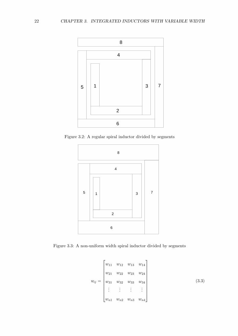
22 CHAPTER 3. INTEGRATED INDUCTORS WITH VARIABLE WIDTH
1
2
3
4
5
6
7
8
Figure 3.2: A regular spiral inductor divided by segments
1
2
3
4
5
6
7
8
Figure 3.3: A non-uniform width spiral inductor divided by segments
wij =
w11 w12 w13 w14
w21 w22 w23 w24
w31 w32 w33 w34
......
......
wn1 wn2 wn3 wn4
(3.3)

3.2. VARIABLE WIDTH INDUCTORS 23
are generated.
In chapter 2 we see that the model components of the integrated inductors are based
on their geometrical parameters. So, given that these parameters are modified by the
introduction of the increase in the metal width, new expressions for the π-model are
needed.
3.2.1 Modeling variable inductors
For determining the analytical expressions for the calculation of the component values
of the π-model is necessary to characterize the width, wi, and the length, li for each segment
of the spiral inductor. The new expression for each component are presented below, based
upon the expressions used to model a regular inductor.
a) Series Inductance, LS
Regarding the π-model inductance, Ls analytical equation 2.2.2 we see that a new way for
evaluating dout must be adopt because of the change in geometry parameters of the metal
strip and expression, and it is given by
dout = din + (2n+ 1)w + (2n− 1)s+ (2n(2n+ 1))∆w (3.4)
But, at this point there is a easier way to calculate the dout of the inductor. Considering
the basic matrices in (3.2) and (3.3), the outer diameter is obtained by
dout = ln3 + wn4 (3.5)
where ln3 is the third segment’s length and wn4 is the last segment’s width of the last
turn. The resulting equation of series inductance for a non-uniform inductor width takes
the same form of the expression for a regular width spiral inductor, replacing the outer
diameter. Thus
LS = K1µ0n2davg
(1 +K2ρ). (3.6)
where the average diameter (davg) depends on the new dout.

24 CHAPTER 3. INTEGRATED INDUCTORS WITH VARIABLE WIDTH
b) Series Resistance, RS
For the evaluation of the series resistance, RS , is necessary to be more careful, since
the maths inherent is a little more complex. As we see in 2.2.3 the expressions that are
used to calculate RS , 2.10 and 2.11, depends on the dimensions of the inductor.
For this purpose two new matrix (3.7) and (3.8) based on the matrices containing the
lengths and widths of each segment are generated (3.2 and 3.3).
lijwij
=
l11w11
l12w12
l13w13
l14w14
l21w21
l22w22
l23w23
l24w24
l31w31
l32w32
l33w33
l34w34
......
......
ln1wn1
ln2wn2
ln3wn3
ln4wn4
(3.7)
lijwij + t
=
l11w11+t
l12w12+t
l13w13+t
l14w14+t
l21w21+t
l22w22+t
l23w23+t
l24w24+t
l31w31+t
l32w32+t
l33w33+t
l34w34+t
......
......
ln1wn1+t
ln2wn2+t
ln3wn3+t
ln4wn4+t
(3.8)
Following our line of thinking, the resultant series resistance is a sum of the resistance
of all segments in particular. In other words, each segment will have a different resistance
because of their different dimensions. Thus,
Rdc =1
σt
n∑i=1
4∑j=1
lijwij
(3.9a)
Rac =k
2σδ
n∑i=1
4∑j=1
lijwij + t
(3.9b)
c) Crossover Capacitance, CS
As we discussed in 2.2.4 the crossover capacitance, CS , connect the inner turn to

3.2. VARIABLE WIDTH INDUCTORS 25
the outside of the spiral inductor. As the width of the metal strip is increased for each
segment, the final metal width is larger than the initial one. The capacity is formed by
two plates with different areas. Assuming that the plates are relatively close that there is
low leakage flux, the capacitance is formed by the lower plate area. Thus, only the initial
width of the metal is considered and this element can be calculated by,
CS = ncw2 εoxtoxM1−M2
(3.10)
d) Oxide Capacitance, Cox
As already discussed in 2.2.5 this capacity is formed between the metal strip and the
silicon substrate. Analyzing the expression we see that this component also depends on
the dimensions of each segment of the coil. Picturing the 3d-image of the spiral inductor
and keeping in mind that we are considering a π-model for each segment we came to the
conclusion that the oxide capacitances of all the segments are in parallel. So the total Cox
is the sum of them all and is given by,
Cox =1
2
εoxtox
n∑i=1
4∑j=1
lijwij . (3.11)
e) Substrate Capacitance, Csi and Resistance, Rsi
The mindset for the evaluation of the new expressions of substrate resistance and
capacitance is similar. From the sectional view we can see that the substrate capacitances
of all segments of the inductor are in parallel resulting in the total substrate capacitance,
Csi =1
2Csub
n∑i=1
4∑j=1
lijwij . (3.12)
For the substrate resistance, the only different is in the parallel of resistances. But
treating these as conductances, we can sum them and invert the result. Thus,
Rsi =2
Gsub
n∑i=1
4∑j=1
1
lijwij. (3.13)

26 CHAPTER 3. INTEGRATED INDUCTORS WITH VARIABLE WIDTH
In section 3.3 a validation of the proposed model by comparasion with ASITIC is
performed.
3.3 Validation of the model
To prove the validity of the proposed model was carried out the following test. Main-
taining constant the geometric parameters of the Table 3.1 and varying the increment
value of width (∆w) the results shown in Table 3.2 were obtained.
Table 3.1: Validity of the optimization modelw (µm) din (µm) n
10.5 134 2.5
Table 3.2: Results comparison with ASITIC
Inductor ∆w (µm) dout (µm) L QModel ASITIC εL (%) Model ASITIC εQ (%)
1 0.0 191 2.01 2.14 6.5 16.30 15 8.02 0.1 194 2.01 2.07 2.9 16.91 17.7 4.73 0.25 199 2.00 2.07 3.5 17.71 18.21 2.84 0.5 205 1.98 2.04 3.1 18.95 19.32 1.95 1.0 220 1.96 2.04 4.3 21.19 20.87 1.56 2.5 257 1.93 1.97 2.0 26.85 23.33 13.1
By the results in Table 3.2 it is quickly to realize that the quality factor increases
with the variation of the width (∆w) and hence the total area of the inductor. Note also
a maximum relative error of around 10% in value compared with ASITIC, from which we
can conclude that our model is a valid layout optimization. In Table 3.3 a ratio between
the increase of the area occupied by the integrated inductor and the increase of the quality
factor is presented.
Table 3.3: Validity of the optimization modelInductor Increased Area (%) Improvement Q (%) Imp.Q/Inc.Area
2 1.8 3.6 23 4.3 7.9 1.844 7.1 14.0 1.975 13.4 23.1 1.736 25.9 39.3 1.52
These results are particularly interesting because we can see a greater increase in the

3.4. OPTIMIZATION 27
quality factor in relation to the occupied area. Following this line of reasoning is to be
expected that we can get a higher quality factor for the same area using variable metal
width spiral inductors.
3.4 Optimization
In order to confirm this theory, a set of square spiral inductors has been designed
using an optimization based tool for the automatic design of spiral inductors [18]. The
efficiency of the tool is accomplished by the inductor π-model. The proposed tool offers
the designer the possibility for obtaining the layout parameters for the desired inductance
value. The solution is obtained considering constraints in the design variables which are
defined by the designer (see Table 3.4).
Table 3.4: Spiral inductor design constraintsParameter Min Step Max
w (µm) 5.0 0.5 100.0∆w (µm) 1 0.25 -
s (µm) 1.5 - -din (µm) 20.0 0.5 200.0
n 1.5 0.5 15.5dout - - 700
These constraints consider not only upper/lower bounds on the variable values, but
also a discretization of the values according to the technology. The technological parame-
ters shown in Table 3.5 were used.
Table 3.5: UMC130 - Technological ParametersParameter Value Parameter Value
ε0 8.85e-12 tox (µm) 600εr 1 Csub (F/m2) 4.0e-6
σ (Ωm) 1/2.65e-8 Gsub 2.43e5
The designer may also choose which performance parameter is to be optimized, such as
maximizing the quality factor, Q, at a predefined operation frequency, or the minimization
of the area occupied. This tool was developed in Matlab [19] and the validity of the solution
obtained was checked against results from simulation with ASITIC simulator.
For the model validation a comparison between results obtained with variable width

28 CHAPTER 3. INTEGRATED INDUCTORS WITH VARIABLE WIDTH
design fixed width designs, for a approximately equal area, is presented. A set of examples
for a spiral inductors at a working frequency of 2.44 GHz was considered.
3.4.1 Example 1
In this example a spiral inductor of 1 nH was considered. The spiral inductor con-
straints design obtained for a fixed width layout as well as for ∆w of 1.5 µm are represented
in Table 2.3. In the Table 3.7, the simulation results obtained with ASITIC for each case
are represented.
Table 3.6: Spiral inductor design constraints for inductance of 1nHInductor w (µm) din (µm) n dout (µm) ∆w (µm)
1 13.0 69 2.5 153 0.02 5.75 42.3 3 153 1.5
Table 3.7: Results comparison with ASITIC
Inductor L Q Improvement (%)Model ASITIC εL (%) Model ASITIC εQ (%)
1 1.00 1.06 7 6.86 6.04 122 1.01 1.03 2 8.13 7.76 5 18
In the last columns the relative improvement in the quality factor from using incre-
mental width is given.
3.4.2 Example 2
In this example a spiral inductor of 2 nH was considered. The spiral inductor con-
straints design obtained for a fixed width layout as well as for ∆w of 0.5, 0.75, 1 and 2
µm are represented in Table 3.8. In the Table 3.9, the simulation results obtained with
ASITIC for each case are represented.
Table 3.8: Spiral inductor design constraints for inductance of 2 nHInductor w (µm) din (µm) n dout (µm) ∆w (µm)
1 10.5 134 2.5 191 0.02 10.0 97 3.0 190 0.753 11.8 67.8 3.5 182 0.54 5.75 96.3 3.0 173 1.05 4.50 96.3 3.0 201 2.0

3.4. OPTIMIZATION 29
Table 3.9: Results comparison with ASITIC
Inductor L Q Improvement (%)Model ASITIC εL (%) Model ASITIC εQ (%)
1 2.00 2.14 6.5 16.3 15.0 8.02 2.01 1.92 4.6 21.3 20.4 4.2 243 2.00 1.91 4.6 22.4 21.3 4.8 274 2.00 1.90 4.8 17.7 17.5 1.0 85 2.00 1.86 7.0 20.7 19.2 7.7 21
In the last columns the relative improvement in the quality factor from using incre-
mental width is given.
3.4.3 Conclusion
The validity of the model was shown through two working examples considering the
design of 1.0nH and 2.0nH inductors at a working frequency of 2.44 GHz. From the
examples presented a quality factor improvement in the order of 10% to 30% may be
obtained, by using variable width for the same chip area.

30 CHAPTER 3. INTEGRATED INDUCTORS WITH VARIABLE WIDTH

Chapter 4
An RF LC Q-Enhanced CMOS
filter
4.1 Introduction
Surface acoustic wave (SAW) filters are applied extensively in today’s communication
equipment. These high performance components have reached a key position in current
communication technology assisting the efforts to increase the spectral efficiency of limited
frequency bands for higher bit rates. During the last decades, driven by the boom of the
wireless technology business, great and important progress in SAW device performance
was made, and a variety of innovative applications were developed. The developments
are based on technological improvements. The reduced size and weight of the complete
system will be an advantage in all kinds of portable electronic products. Moreover, re-
ceiver architectures in telecommunication systems use higher IF frequencies to improve
the interfering signal rejection. The allocations of radio frequency spectrum has led to
the development of small and low-cost wireless products. The commercial sector has re-
sponded with increasing levels of integration. Researchers have attempted to design high
Q bandpass filters by enhancing lossy integrated inductors. Shunt mounted resonator,
composed of an inductor and capacitor in parallel is presented to realize RF bandpass
filter. The design of the integrated on-chip 1.2V 2.44 GHz Q-enhanced LC filter using
silicon CMOS process is presented in this chapter.
31

32 CHAPTER 4. AN RF LC Q-ENHANCED CMOS FILTER
4.2 Tuned Amplifiers
Highly selective bandpass filters have long been implemented with tuned amplifiers. In
figure 4.1 the amplitude response of a tuned amplifier is represented, which may be char-
acterized by the central frequency, ω0, and the 3-dB bandwidth, B. In many applications,
the 3-dB bandwidth is less than 5% of ω0 [20]
Gain (dB)
Frequency (Hz)f1 f2f0
Cen
ter
freq
uecy
3 dBBandwidth
Figure 4.1: Frequency response of a tuned amplifier
The basic principle in the design of tuned amplifiers is the use of parallel RLC circuit
as the load, or at the input, of a BJT or a FET amplifier. In figure 4.2 a MOSFET class
A amplifier, having a tuned-circuit load is illustrated. For the sake of simplicity, the bias
details are not included. Since this circuit uses a single tuned circuit, it is known as a
single-tuned amplifier [20].
Vi
RL CL L
Vo
(a)
Vi R C LgmVi Vo
+
-
(b)
Figure 4.2: The basic principle of tuned amplifier is illustrated using a MOSFET with atuned circuit load. Bias details are not shown.
The amplifier small signal equivalent circuit is represented in figure 4.2 where R de-

4.2. TUNED AMPLIFIERS 33
notes the parallel equivalent of RL and the MOSFET output resistance ro, and C is the
parallel equivalent of CL and the FET output capacitance (usually very small). From the
equivalent circuit we may write,
Vo = −gmViYL
= − gmVi
sC + 1R + 1
sL
(4.1)
The voltage gain is a second-order bandpass function and can be expressed as
VoVi
= −gmC
s
s2 + 1RC s+ 1
LC
(4.2)
We may thus conclude that the tuned amplifier has a center frequency of
ω0 =1√LC
(4.3)
a 3-dB bandwidth of
B =1
RC(4.4)
a quality factor of
Q ≡ ω0
B= ω0RC (4.5)
and a center-frequency gain of
Vo(jω0)
Vi(jω0)= −gm
C
jω0
(jω0)2 +Bjω0 + ω20
= −gmC
jω0
(−ω0)2 +Bjω0 + ω20
= −gmR (4.6)
In the case of wireless transmitters it is necessary to implement filters of very high
selectivity. In these cases LC filters may be employed. The use of integrated inductors
in CMOS technology raises problems for the implementation of high selectivity LC filters
selectivity due to the difficulty of designing coils with high quality factor operating at RF
frequencies. For wireless applications fully integrated highly selective bandpass filters are
needed with quality factor in the order of 30. In this cases a Q-enhanced LC topology

34 CHAPTER 4. AN RF LC Q-ENHANCED CMOS FILTER
must be adopted. In the next section a brief description of a Q-enhancement technique
using a negative active resistance gm will be presented.
4.3 Principles of Q enhancement
Q enhancement has long been used in LC circuits for signal amplification, signal
selection and for generating stable oscillation [21]. In this section, our discussion is focused
on the Q-enhancement in integrated LC filters. If a high selectivity LC resonator is desired
some form of Q-enhancement is needed to increase the quality factor of resonators designed
with lossy on-chip resonator.
Regardless of the coupling mechanism between the resonators, losses associated with
the on-chip reactive components change the center frequency and the loaded quality factor
of the filter. Having estimated and modeled the total resistive loss of the resonator, a active
device to create a negative resistance, (-1/Gneg), exactly the opposite caused by the losses
of reactive components can be added to compensate its effect as shown in figure 4.3.
Although methods that include phase-shifted current feedback via coupled inductors
have been investigated, the direct use of active devices as negative resistors is the preva-
lent Q-enhancement technique [3]. This way, combining the reactive component with a
negative resistance, the real part of the total impedance is reduced, eliminated or even
made negative, depending on the value of the negative resistance used. We can say that
the quality factor of the original lossy component can be improved (enhanced) by the
negative resistance and resulting component can replace the original used in the LC filter.
This Q-enhancement technique is shown in figure 4.4.
LC
Rs
C L R C L Rp -R
Figure 4.3: Active Q-enhancement using negative resistance
Assuming that a lossy inductor with a quality factor of Q0 can be simplistically mod-
elled (4.3) by an inductor L with an series resistance RS , we may consider,

4.3. PRINCIPLES OF Q ENHANCEMENT 35
Visine
C
Ls
Rs
-Rneg
Gin
Gneg
Vout
Lp ≈ Ls Rp = (1 + Q0*Q0) Rs
Figure 4.4: Q-enhancement technique applied to a RLC filter
RS =ωL
Q0(4.7)
These losses can be compensated by connecting the negative resistance in parallel with
the LC tank. Assuming that the quality factor of the tank capacitance is much larger than
the inductor, the series combination of the inductor (LS) and its loss RS can be modeled
as a parallel combination of an inductance LP and resistance RP given by
LP = LS(1 +1
Q20
) ≈ LS = ωLQ0 (4.8)
and
RP = RS(1 +Q20) = ωLQ0 (4.9)
If the inductor quality factor Q0 is large enough then, LP ∼= L. The frequency response
of the filter in the figure 4.5 can be approximated as
H(s) =Vo(s)
Vin(s)∼=
Gm
GP −Gneg + 1sLP
+ sC(4.10)

36 CHAPTER 4. AN RF LC Q-ENHANCED CMOS FILTER
L L
Vout
M4 M5
C
M6
Vin + Vin-
Vgm-Gneg
M2
M3
M1 Vq
Gin
Rp Lp
Vdd
Figure 4.5: Q-enhanced LC bandpass filter
or
H(s) =Vo(s)
Vin(s)∼=
−GmC s
s2 +GP−Gneg
C + 1LC
=−A0
ω0Q s
s2 + ω0Q s+ ω2
0
(4.11)
From which we may conclude that the central frequency will be given by
ω0 =1√LC
(4.12)
Also from equation 4.11 we may conclude that the filter quality factor will be given
by
Q =C 1√
LC
GP −Gneg=
√CL
(GP −Gneg)(4.13)
The filter central gain, A0 will be given by
A0 =GmC
Q
ω0=
GmGP −Gneg
(4.14)

4.3. PRINCIPLES OF Q ENHANCEMENT 37
and the bandwidth, B can be described as:
B =ω0
Q=
√1LC (GP −Gneg)√
CL
(4.15)
As 4.12 shows, the quality factor of the inductor (Q0) does not modify the center
frequency but increases the Q of the resonator. Thus at high frequencies, due to the
higher losses, a larger Gneg is required which results in changing both Q. Note that the
equation 4.13 is valid only around the LC tank’s resonant frequency, due to the fact that
the equivalent parallel conductance from the inductor loss varies with frequency.
Considering the circuit implementation of a second-order Q-enhanced LC filter in
4.5, the center frequency tuning is achieved through varactors which are PMOS transis-
tors implemented in separate wells (in an n-well technology) and with their drain/source
terminals connected together to the well terminal. The capacitance seen by the gate is
adjusted by changing the voltage Vf and exploiting the variation of the gate capacitance
when the transistor goes from weak inversion to the accumulation region.
The operation of a MOSFET can be separated into three different modes, depending
on the voltages at the terminals. In the saturation or active mode the switch is turned
on when Vgs > VT and Vgs > Vds − VT and a channel is created which allows current to
flow between the drain and the source. The drain current is weakly dependent upon drain
voltage and controlled primarily by the gate-source voltage, and modeled approximately
as:
Id =1
2µnCox
W
L(Vgs − VT )2 (4.16)
A key design parameter, the MOSFET transconductance gm is:
gm =∂Id∂Vgs
=∂
∂Vgs
(1
2µnCox
W
L(Vgs − VT )2
)= µnCox
W
L(Vgs − VT ) (4.17)
The cross coupled transistor M2-M3 form the negative transconductance -Gneg which
based on equation 4.13 changes the quality factor of the filter. The transconductance Gneg

38 CHAPTER 4. AN RF LC Q-ENHANCED CMOS FILTER
is dependent on the control voltage, Vq. Considering that the transistors M2 and M3 are
equal, we know that,
ID2,3 =1
2ID1 ⇔
⇔ 1
2µnCox
(W
L
)2,3
(Vgs − VT )2 =1
2
1
2µnCox
(W
L
)1
(Vq − VT )2
⇔ (Vq − VT )2 =1
2
(WL
)1(
WL
)2,3
(Vq − VT )2 (4.18)
Using the equation 4.16 results in,
Gneg = µnCox
√1
2
(W
L
)1
(W
L
)2,3
(Vq − VT ) (4.19)
where (W/L)2,3 and (W/L)1 refer to the (W/L) ratios of M2,3 and M1 in figure 4.5,
respectively. To simplify the formulas we consider that
βq = 0.5µCox
√0.5
(W
L
)2,3
(W
L
)1
(4.20)
so,
Gneg = βq(Vq − VT ) (4.21)
Following the same reasoning, the control voltage Vgm changes the transconductance
Gm of the input differential pair M4-M5 thus, changing the peak amplitude gain A0 of the
filter while keeping the Q invariant. Note that Gm as a function of Vgm can be expressed
as
Gm = βm(Vgm − VT ) (4.22)
where
βm = 0.5µCox
√0.5
(W
L
)4,5
(W
L
)6
(4.23)
and (W/L)4,5 and (W/L)6 refer to the (W/L) ratios of M4,5 and M6 in figure 4.5, respec-

4.4. INTEGRATED FILTERS DESIGN 39
tively.
Thus using 4.19 and 4.22 the peak amplitude gain A0 defined in equation 4.10, can
be expressed as,
A0 =Gm
GP −Gneg=
2βm(Vgm − VT )
GP − βq(Vq − VT ). (4.24)
In similar way the quality factor Q can be expressed as,
Q =
√CL
GP − βq(Vq − VT ). (4.25)
4.4 Integrated Filters design
Like analog circuit in general, radio-frequency integrated circuit (RFIC) designs suffer
from required trade-offs that include linearity, noise, power, frequency, gain and supply
voltage [1].
The circuit design investigated in this work introduces a loss-compensated second-
order RF filter that is to be implemented in a standard 0.13µm CMOS process. This filter
uses an on-chip resonant tank comprised of an spiral integrated inductor and a capaci-
tance that is a combination of the1 circuit parasitics as well as specifically incorporated
passive elements. Loss compensation is achieved by using a transconductor that emulates
negative resistance. This particular topology is a circuit solution for the Q-enhancement
as explained in the section 4.3.
An operational objective of this work is to implement a Q-enhanced LC filter with
center frequency of 2.44 GHz and 3-dB bandwidth of 84 MHz and a maximum gain of 15
dB. One of the trade-offs suffered when incorporating active on-chip filters to replace the
passive off-chip counterparts is in the required power consumption. In wireless devices
circuit topologies that maximize the time of operation are a primary concern.
This section provide details regarding the Q-enhanced LC filter including circuit oper-
ational characteristic, design methodology, physical layout considerations and simulation
results.
Components values for the inductors and capacitors of the resonant tank were chosen

40 CHAPTER 4. AN RF LC Q-ENHANCED CMOS FILTER
to realize the specifications of the filter. In this case, we have,
ω0 = 2π · 2.44 · 109 = 1.5331 · 1010rad/s (4.26)
and
B = 2π · 84 · 106rad/s (4.27)
In order to prove the advantage of using optimized integrated spiral inductors two
designs of the LC filter were performed. So, a comparison between the non-optimized
(fixed width) and the optimized integrated inductor (variable width) is performed. An
inductor of 1 nH was considered to implement this filter since it is a reasonable value for
the envisaged central frequency. In table 4.1 the layout dimensions as well as the values of
the inductance and resistance of the inductors used to implement the filter is presented.
Table 4.1: Inductor of 1 nH used in filterw (µm) din (µm) n dout (µm) ∆w (µm) L(nH) R(Ω) Q
7.75 68.8 2.5 112 0.0 1.00 1.4 11.05.5 47.5 3.0 114 0.75 1.00 1.133 13.55
Its possible to size the values of the transconductance, Gneg, and of the capacitance
solving the following system of equations given by 4.12 and 4.15. Thus,
ω0 =
√1LC
B =GP−Gneg
C
(4.28)
results in
Table 4.2: Values of the Gneg and C
Regular inductor Optimized inductor
Gneg (mS) 3.7 2.6C (pF) 4.25 4.25
In order to obtain this values of the Gneg we have to size the dimensions of the
transistor MOS. By equation 4.19 demonstrated in the previous section we have that,

4.4. INTEGRATED FILTERS DESIGN 41
Gneg = µCox
√0.5
(W
L
)1
(W
L
)2,3
(Vq − VT ) (4.29)
To simplify the sizing of transistors to obtain the desired Gneg, it was decided to design
the three transistors with the same size and L = L1 = L2 = L3 = 600 µm since the length
should be greater than three times the minimum allowed by the technology (3 × 130µm).
Substituting in the above equation, the width of transistor MOS in order to obtain the
value of the Gneg is given by,
W =GnegL
µnCox√
0.5(Vq − VT )(4.30)
For the technological parameters we have considered µnCox equals to 309 · 10−6 µm
and a VT is 0.27 V. These values were obtained from simulations in Cadence. The value of
Vq is 0.8 V as a way of having the transistors working in moderate inversion. Given that
we are now able to determine the exact value for the width of the transistor. The table
4.3 shows the value of the W for both regular and optimized inductor.
Table 4.3: Value of the Width of the transistors MOSRegular inductor Optimized inductor
MOS Width (µm) 18.7 13.14
Now we must design the size of the transistors M4, M5 and M6 in order to obtain the
desired gain, A0. Assuming we want a gain of 15dB, by equation 4.24 we know that,
Gm = (Gp −Gneg)A0 (4.31)
In the previous section we demonstrated in equation 4.22 that,
Gm = µnCox
√0.5
(W
L
)6
(W
L
)4,5
(Vgm − VT ) (4.32)
Again, to simplify the sizing of transistors to obtain the desired gm, it was decided to
design the three transistors with the same size and L = L4 = L5 = L6 = 600 µm, µCox

42 CHAPTER 4. AN RF LC Q-ENHANCED CMOS FILTER
equals to 309 · 10−6, VT is 0.27 V and Vgm is 0.8 V.
Substituting in the above equation, the width of transistor MOS in order to obtain
the value of the Gneg is given by,
W =gmL
µnCox√
0.5(Vgm − VT )(4.33)
The table 4.3 shows the value of the W extracted from equation 4.33 for both regular
and optimized inductor.
Table 4.4: Value of the Width of the transistors MOS (4,5,6)Regular inductor Optimized inductor
Gm (mS) 12.1 12.3MOS Width (µm) 62.8 63.6
To verify the design of the Q-enhanced RF bandpass filter, the filter was simulated in
a UMC130 standard CMOS process using the Cadence design environment.
4.4.1 Simulation results
In this section the results of the simulations, namely the passband response are pre-
sented. Two implementations of the filter were performed. The first implementation using
a regular integrated inductor, ie, with fixed width. In the second implementation an opti-
mized integrated inductor with non-uniform metal width was used proving that the filter
maintain the good performance with this type of inductor.
As illustrated in figure 4.6, for the simulation of the inductor the corresponding pi-
model was used. As previously explained, the value of the π-model resistance RS is
frequency dependent. Yet, since we are considering its inclusion in a highly selective filter,
using a fixed RS value obtained for the center frequency is a good approach.
4.4.2 gmLC filter with regular integrated inductor
The figure 4.6 shows the schematic of a second order Q-enhanced LC filter using
a regular integrated inductor. Using the input values of the table 4.1 presented in the
previous section for the case of ∆w= 0 we obtained the following values of the model-π
components.

4.4. INTEGRATED FILTERS DESIGN 43
M4 M5
C
M6
M2
M3
M1
Vin+sine
Vgm
Vin-sine
Vdd
Vq
spiral in
du
ctorsp
iral
ind
uct
or
Ls
Rsi Csi
Rs
Cox
Rsi1 Csi
Cox
Cs
Figure 4.6: A 2nd Q-enhanced on-chip LC bandpass filter
Table 4.5: Model π components valuesLS (H) RS (Ω) CS (F) Cox (F) Csi (F) Rsi (Ω)
1e-9 1.4 0.751e-15 22.8e-15 0.526e-15 5.61e8
The filter passband response measurements performed using AC analysis in the Ca-
dence simulator is shown in figure 4.7.
The measured gain of 12.65 dB at the center frequency of 2.405 GHz is lower than the
originally designed filter gain in approximately 2.5 dB. Figure 4.7 also illustrates that the
filter center frequency is shifted slightly lower than the required f0 of 2.44 GHz specified
for the targeted Bluetooth application, falling within 1.43% of the design goal. The table
4.6 compares the predicted and the simulated results.
Analysing the results presented in the table 4.6 it could be concluded that the method
used to design the filter is quite acceptable since the results are close to the desired results.

44 CHAPTER 4. AN RF LC Q-ENHANCED CMOS FILTER
2 2.1 2.2 2.3 2.4 2.5 2.6 2.7 2.8 2.9
x 109
−10
−5
0
5
10
15
fc: 2.405e+009A: 12.65
Frequency (Hz)
Gai
n (d
B)
AC Response
Figure 4.7: Frequency response of the RF LC Q-enhanced filter using a regular spiralinductor
Table 4.6: Simulation resultsTargeted values Achieved values εr(%)
Gneg (mS) 3.7 3.87 4.59Gm (mS) 12.1 11.14 7.93fc (GHz) 2.44 2.405 1.43
BW (MHz) 84 90 7.14Quality factor 29 26.72 8
Output Gain (dB) 15 12.65 15.67
The largest relative error was obtained in the output gain of approximately 16%. This
errors were already expected since the parasitic capacities of the transistors are not taken
into account and the quadratic model of MOS transistors is not the most appropriate for
the technology used.
4.4.3 gmLC filter with optimized integrated inductor
For the implementation of the second order Q-enhanced LC filter using a optimized
integrated inductor studied in chapter 3 the filter design used was the same (see figure
4.6, but now using the input values of the table 4.1 for the case of ∆w= 0.75. The table
4.7 shows the value of the model-π components obtained.
The frequency response of the filter is shown in figure 4.8.
The measured gain of 13.07 dB at the center frequency of 2.417 GHz is lower than the

4.4. INTEGRATED FILTERS DESIGN 45
Table 4.7: Model π components valuesLS (H) RS (Ω) CS (F) Cox (F) Csi (F) Rsi (Ω)
1e-9 1.13 0.504e-15 30.1e-15 0.691e-15 4.28e8
2 2.1 2.2 2.3 2.4 2.5 2.6 2.7 2.8 2.9
x 109
−10
−5
0
5
10
15
fc: 2.417e+009A: 13.07
Frequency (Hz)
Gai
n (d
B)
AC Response
Figure 4.8: Frequency response of the RF LC Q-enhanced filter using an optimized spiralinductor
originally designed filter gain of approximately 2 dB. Figure 4.7 also illustrates that the
filter center frequency is shifted slightly lower than the required f0 of 2.44 GHz specified
for the targeted Bluetooth application, falling within 0.94% of the design goal.
The table 4.8 compares the predicted and the simulated results
Table 4.8: Simulation resultsTargeted values Achieved values εr(%)
Gneg (mS) 2.6 2.72 4.62Gm (mS) 12.3 11.28 8.2fc (GHz) 2.44 2.417 0.94
BW (MHz) 84 88 4.76Quality factor 29 27.5 5
Output Gain (dB) 15 13.12 12.53
By the results in table 4.8 we can see a close agreement between the target and the
achieved values. The largest relative error was obtained in the output gain of approxi-
mately 12.5%.
In the following subsection a comparison of the performance of the filter using the two
types of integrated inductors is performed.

46 CHAPTER 4. AN RF LC Q-ENHANCED CMOS FILTER
4.4.4 Conclusions
In order to get a more appropriate comparison between the two implementations of the
filters, a fine tuning was carried out with the purpose of the frequency response of the filters
became identical and in order to meet the desired specifications. The inverse proportional
relation between Gm of the input and Gneg of loss compensation negative resistance must
be taken into account. For example, suppose that Gneg is decreased for lower Q, then Gm
should be increased to keep the gain constant. The center frequency shifting is mainly due
to the parasitic capacitances of the transistors. This can be compensated by reducing the
value of the capacitance C. In this way, we can achieve the synchronized coarse tuning of
f0, gain, the -3 dB bandwidth and the corresponding Q. The fine tuning can be done in
the following steps by considering the weak interaction between f0, gain and Q, and the
control variables such as Gm and Gneg:
1. Tune C for f0 fine tuning.
2. Tune Gneg for fine bandwidth tuning and the consequent fine filter Q tuning.
3. Tune Gm for fine gain tuning.
The table 4.9 presents the values of the parameters changed to the fine tuning.
Table 4.9: Fine tuning resulting values
Parameter Regular inductor Optimized inductorBefore After Before After
C (pF) 4.25 4.06 4.25 4.10W1,2,3 (µm) 18.7 19.7 13.14 14.1W4,5,6 (µm) 62.8 71.5 63.6 71.5
In figures 4.9 and 4.10 the AC desired response of the filter is presented.
The table 4.10 shows the performance comparison of RF integrated LC filter for the
two types of integrated inductors.
The comparison table demonstrates that the proposed RF filter has lower power-
consumption when using the optimized (variable width) inductors in order of 10%. This
reduction is due to decreased resistance of the optimized inductor. A smaller resistance
requires a Gneg smaller reducing the size of the transistors.

4.4. INTEGRATED FILTERS DESIGN 47
2 2.1 2.2 2.3 2.4 2.5 2.6 2.7 2.8 2.9
x 109
−10
−5
0
5
10
15
20
fc: 2.441e+009A: 15.01
Frequency (Hz)
Gai
n (d
B)
AC Response
Figure 4.9: Frequency response of the RF LC Q-enhanced filter using a regular spiralinductor
2 2.1 2.2 2.3 2.4 2.5 2.6 2.7 2.8 2.9
x 109
−10
−5
0
5
10
15
20
fc: 2.441e+009A: 15.04
Frequency (Hz)
Gai
n (d
B)
AC Response
Figure 4.10: Frequency response of the RF LC Q-enhanced filter using a regular spiralinductor
Table 4.10: Simulation resultsPerformance Parameters Regular Inductor Optimized Inductor
Center frequency (GHz) 2.441 2.4413 dB Bandwidth (MHz) 84 84
Maximum Gain in passband (dB) 15.01 15.04Supply Voltage (V) 1.2 1.2DC Current (mA) 5.66 5.09
DC consumption (mW) 6.79 6.11

48 CHAPTER 4. AN RF LC Q-ENHANCED CMOS FILTER

Chapter 5
Conclusions
The design and simulation of a 2.44 GHz in standard 0.13µm CMOS fully integrated
second-order Q-enhanced LC bandpass filter have been introduced and verified, which
demonstrate that the RF bandpass filter can achieve a high selectivity.
In a fully integrated LC bandpass filter the integrated spiral inductor is an important
performance-limiting component in RF circuits. This work is devoted to the study of RF
integrated inductors as planar square spirals in silicon-based technology. The degradation
of the Q-factor presents great challenge for the designers. The inductor series resistance
is analysed taking into account both ohmic losses, due to conduction currents and mag-
netically induced losses, due to eddy currents.
A method to improve the Q factor of the inductor is presented. The method is based
on the layout optimization being the width of the metal strip used to perform the main
variable of the optimization process. For a given frequency of operation, the application
of the proposed method minimizes the series resistance of each segment of the inductor
coil, leading to a multistrip-width layout.
The proposed method is used to optimize the layout of square spiral inductors for
the 0.13µm CMOS technology. The comparison of the results obtained for the optimized
layout with those of other non-optimized (occupying the same chip’s area) reveals that the
application of the proposed model leads to a significant increase in the inductor Q factor.
From the examples presented a quality factor of 20% to 30% to may be obtained by using
variable metal width.
49

50 CHAPTER 5. CONCLUSIONS
A 2nd order filter with center frequency ate 2.44 GHz was designed using integrated
spiral inductors. The quality of on-chip reactive components is a challenge in the design of
such filter, since the losses and the parasitics in those components can result in frequency
response distortion and need for active components like negative resistors to compensate
the losses. In order to validate the performance of the optimized inductor a comparison
as performed between inductors with and without layout optimization. The results shows
that with a power supply of 1.8 V the filter using the optimized inductor has a lower power
consume in order of 10%.
With this work it has been verified through simulation that the design of a Q-enhanced
LC filter in a new systematic way to achieve gain, center frequency, and filter Q tuning
capability.

Bibliography
[1] W. A. Gee, CMOS Integrated LC Q-Enhanced RF Filters for wireless receivers. PhD
thesis, Georgia Institute of Technology, 2005.
[2] P. Almeida, P. Pereira, and M. H. Fino, “Using variable width rf integrated induc-
tors for quality factor optimization,” in Technological Innovation for the Internet of
Things, vol. 394, pp. 619–627, Springer Berlin Heidelberg, 2013.
[3] F. Bahmani, High Performance RF and baseband building blocks for wireless receivers.
PhD thesis, Texas A and M University, 2006.
[4] S. Mohan, M. del Mar Hershenson, S. Boyd, and T. Lee, “Simple accurate expressions
for planar spiral inductances,” Solid-State Circuits, IEEE Journal of, vol. 34, pp. 1419
–1424, oct 1999.
[5] G. Zardo, “A 4th order cmos 0,13 µm integrated lc filter for rf receivers,” Master’s
thesis, Ecole Polytechnique, 2006.
[6] W. Yu, “Optimization of spiral inductors and lc resonators exploiting space mapping
technology,” Master’s thesis, McMaster University, 2006.
[7] J. Lopez-Villegas, J. Samitier, C. Cane, P. Losantos, and J. Bausells, “Improvement
of the quality factor of rf integrated inductors by layout optimization,” Microwave
Theory and Techniques, IEEE Transactions on, vol. 48, pp. 76 –83, jan 2000.
[8] J. Peters, “Design of high quality factor spiral inductors in rf mcm-d,” Master’s thesis,
Massachusetts Institute of Technology, 2004.
51
52 BIBLIOGRAPHY
[9] C. Yue, C. Ryu, J. Lau, T. Lee, and S. Wong, “A physical model for planar spiral
inductors on silicon,” in Electron Devices Meeting, 1996. IEDM ’96., International,
pp. 155 –158, dec. 1996.
[10] S. Jenei, B. Nauwelaers, and S. Decoutere, “Physics-based closed-form inductance
expression for compact modeling of integrated spiral inductors,” Solid-State Circuits,
IEEE Journal of, vol. 37, pp. 77 –80, jan 2002.
[11] M. Raieszadeh, “High-q integrated inductors on trenched silicon islands,” Master’s
thesis, Georgia Institute of Technology, 2005.
[12] M. Park, C.-H. Kim, C. S. Kim, M.-Y. Park, S.-D. Kim, Y.-S. Youn, and H. K. Yu,
“Frequency-dependent series resistance of monolithic spiral inductors,” Microwave
and Guided Wave Letters, IEEE, vol. 9, pp. 514 –516, dec 1999.
[13] Y.-S. Choi and J.-B. Yoon, “Experimental analysis of the effect of metal thickness on
the quality factor in integrated spiral inductors for rf ics,” Electron Device Letters,
IEEE, vol. 25, pp. 76 – 79, feb. 2004.
[14] J. Aguilera and R. Berenguer, Design and Test of Integrated Inductors for RF Appli-
cations. Kluwer Academic Publishers, 2004.
[15] J. Chen and J. J. Liou, “On-chip spiral inductors for rf applications: An overview,”
Journal of Semiconductor Technology and Science, vol. 4, no. 3, pp. 149–167, 2004.
[16] H. Heng-Ming, “Improving the quality factor of a broadened spiral inductor with
arithmetic-progress step width,” Microwave and Optical Technology Letters, vol. 45,
no. 2, pp. 118–120, 2004.
[17] J. Liu, Y. Shi, X. Wen, D. Chen, T.-X. Luo, H. Huang, H. Ye, and Y. Wang, “On-
chip spiral inductor with novel gradually changed structure,” Microwave and Optical
Technology Letters, vol. 50, no. 8, pp. 2210–2213, 2008.
[18] P. Pereira, M. H. Fino, F. Coito, and M. Ventim-Neves, “Gadisi – genetic algo-
rithms applied to the automatic design of integrated spiral inductors.,” (Caparica,
Pt), pp. 515–522, Springer, 2010.

BIBLIOGRAPHY 53
[19] P. Pereira, H. Fino, F. Coito, and M. Ventim-Neves, “Adisi- an efficient tool for
the automatic design of integrated spiral inductors,” in Electronics, Circuits, and
Systems, 2009. ICECS 2009. 16th IEEE International Conference on, pp. 799 –802,
dec. 2009.
[20] A. S. Sedra and K. C. Smith, Microelectronic Circuits. Cambridge, MA, USA: Oxford
University Press, 1991.
[21] Y. Sun, ed., Active filters using integrated inductors, vol. 14 of Circuits, Devices and
Systems, The Institution of Engineering and TechnologySpringer, 2002.

54 BIBLIOGRAPHY

Appendix A
Publications
In this appendix the article made throughout this thesis are presented. The article
”Using Variable Width RF Integrated Inductors for Quality Factor Optimization”, was
submitted in the 4th IFIP WG 5.5/SOCOLNET Doctoral Conference on Computing,
Electrical and Industrial Systems, DoCEIS 2013. This article is based on all the work
done throughout the project of this master thesis.
55
Using Variable Width RF Integrated Inductors for
Quality Factor Optimization
Pedro Almeida1, Pedro Pereira1, Helena Fino1
1 Departamento de Engenharia Electrotécnica, Faculdade de Ciências e Tecnologia, FCT,
Universidade Nova de Lisboa, 2829-516 Caparica, Portugal.
[email protected], hfino, [email protected]
Abstract. The advancement of CMOS technology led to the integration of more complex functions. In the particular of wireless transceivers, integrated LC tanks are becoming popular both for VCOs and integrated filters [1]. For RF applications the main challenge is still the design of integrated inductors with the maximum quality factor. For that purpose, tapered, i.e., variable width inductors have been proposed in the literature. In this paper, analytical expressions for the determination the pi-model parameters, for the characterization of variable width integrated inductors are proposed. The expressions rely exclusively on geometrical and technological parameters, thus
granting the rapid adaptation of the model to different technologies. The results obtained with the model are compared against simulation with ASITIC, showing errors below 10%. The model is then integrated into an optimization procedure where inductors with a quality factor improvement in the order of 20-30% are obtained, when compared with fixed width inductors.
Keywords: Inductor layout optimization, variable metal width,
integrated RF inductor
1 Introduction
During the last years the worldwide market on communications has experienced an
ever-growing demand for integrated systems with scaling down dimensions and
increased functionality. In the particular case for RF communication circuits,
integrated spiral inductors are widely used, notwithstanding their poor performance
and their subsequent negative impact on the circuit efficiency at high frequencies.
This poor performance is due to the large effect the technology parasitics have on the
small value of inductance usually required. As a result, significant effort has been
employed in investigating silicon planar inductors, their associated models and
methods of improving their performance [1-3]. Regarding layout optimization, non-uniform metal width is proposed, as a way of
increasing the inductor quality factor [4, 5]. The main objective of this methodology
is to reduce the influence of magnetically induced losses in the inner turns of the

spiral where the magnetic field reaches its maximum. By reducing the line width
toward the center of the spiral a minimization of the series resistance of the inductor
coil, taking into account both Ohmic losses due to conduction currents, and
magnetically induced losses due to Eddy currents, is obtained. Although several
promising results have been reported, a fully analytical characterisation of the
inductor, leading to perfect understanding of the device performance limitations, is
needed so that optimized designs may be obtained.
In this paper analytical expressions for the evaluation of the inductor model parameters are proposed. These expressions rely exclusively on technological
parameters and on the geometrical characterization of each inductor segment. The
proposed model is used for the optimization-based design of several inductors, where
the advantage of using tapered topologies is well pointed out.
The remain of the paper is organized as follows. The novelty introduced by this
paper, is highlighted in Section 2. In this section the basic inductor model is
introduced and then, the adaptation of the model for variable width inductors is
carefully described. Section 3 is dedicated to the description of several working
examples. Finally, conclusions are offered in Section 4.
2 Relationship to Internet of Things
Internet of things relies on the interconnections of a large number of heterogeneous
cooperating devices. The development of these devices has been made possible due to
the rapid evolution of electronic technologies, enabling the implementation complex
functions, in smaller and more rapid circuits. To cope with the necessity of minimizing the power consumption of such systems, new design methodologies must
be adopted. In the particular case of communications services, RF integrated inductors
are becoming popular elements. Yet, designing integrated inductors for RF
applications is a challenging process where a set of correlated geometrical parameters
must be obtained, leading to the need of using optimization-based design
methodologies.
The main objective of the work described is the optimization of the spiral inductors
quality factor, by using variable width inductors
The novel contributions of this paper are as follows:
It proposes a set of analytical expressions for the evaluation of the pi-model parameters, for variable width integrated inductors. The proposed expressions
depend exclusively on the technological parameters and on the geometric
characterization of each segment of the inductor.
It proposes an efficient optimization-based design for nano-CMOS planar spiral
inductor, based in analytical models, instead of using an electromagnetic
simulation based approach;
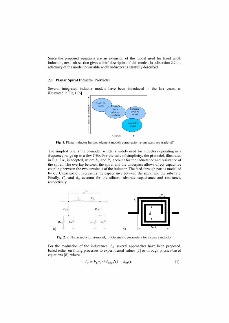
Since the proposed equations are an extension of the model used for fixed width
inductors, next sub-section gives a brief description of this model. In subsection 2.2 the
adequacy of the model to variable width inductors is carefully described.
2.1 Planar Spiral Inductor Pi-Model
Several integrated inductor models have been introduced in the last years, as
illustrated in Fig.1 [6]
Fig. 1. Planar inductor lumped element models complexity versus accuracy trade-off
The simplest one is the pi-model, which is widely used for inductors operating in a
frequency range up to a few GHz. For the sake of simplicity, the pi-model, illustrated
in Fig. 2.a., is adopted, where Ls, and Rs. account for the inductance and resistance of
the spiral. The overlap between the spiral and the underpass allows direct capacitive coupling between the two terminals of the inductor. The feed-through part is modelled
by Cs. Capacitor Cox represents the capacitance between the spiral and the substrate.
Finally, Csi and Rsi account for the silicon substrate capacitance and resistance,
respectively.
a) b)
Fig. 2. a) Planar inductor pi-model; b) Geometric parameters for a square inductor.
For the evaluation of the inductance, LS, several approaches have been proposed,
based either on fitting processes to experimental values [7] or through physics-based
equations [8], where
(1)

Given that,
(2.a)
(2.a)
(2.b)
Where n is the number of turns, s is the track-to-track distance, and w is the track width. Finally, k1 and k2, are coefficients allowing the model to be adapted to several inductor shapes.
The evaluation of the spiral resistance, Rs, is obtained by [9]
(3)
Where,
(4.a)
(4.b)
And σ and t are the metal conductivity and thickness, respectively. The metal length, l, is obtained with [10]
(5)
And the skin depth, , may be determined by [11]
(6)
For the evaluation of the capacitance, Cs, all overlap capacitances are considered and given by [12].
(7)
Where εox is the oxide permittivity, nc is the number of overlaps and is the oxide thickness between the spiral upper and lower metal. The parasitic capacitance, Cox, between the spiral metal and the silicon substrate, is estimated with [12]
(8)
Where tox is the thickness of the SiO2 between the inductor and the substrate and lw defines the area of the spiral. Finally the Substrate resistance, Rsi, and capacitance Csi, are obtained with 11
(9)
(10)

where σsi and hsi are the substrate conductivity and height, respectively.
This model has been extensively used in an optimization-based tool for inductor
design [13] yielding solutions with very good accuracy when compared with results
obtained with ASITIC .
2.2- Variable Width Inductor Model
Variable width inductor layout has been proposed as a way of maximizing the quality
factor of integrated inductors. In this work, square inductors, where each segment
shows a width increment of w, as illustrated in Fig.3. , are considered.
Fig. 3. Variable width square inductor
Since each segment will show an increment on both width and length new
equations will be proposed, relying on the dimensions of each segment of the
inductor. The width of a segment may be evaluated with
(11)
Where ni is the number of the segment, and w is the initial metal width.
In this work, the basic structure for supporting all the inductor segments
characterization is a matrix of five columns (one for each segment per turn) and n
lines (one per inductor turn). Initially, a matrix containing every segment length, lij as
(12)
Is generated. Then a matrix containing every segment width, wij

(13)
is generated.
Regarding the pi-model inductance, LS, a new way for evaluating dout must be
adopted. Considering the basic matrixes in (12), (13), dout may be obtained by
(14)
For the evaluation of RS, (4.a) and (4.b) are replaced by
(15.a)
(15.b)
For this purpose the two new matrix (15.a) and (15.b) are generated containing each
segment geometrical information for Rdc and Rac
(16)
(17)
Finally (8) , (9) and (10) are replaced by

(18)
(19)
(20)
For which an auxiliary matrix containing the area of each segment is considered.
4 Variable Inductor Working Example
In order to confirm the validity of the proposed layout optimization method, a set of
square spiral inductors has been designed. Three examples, considering the design of
1nH, 1.5nH and 2nH inductors at a working frequency of 1GHz will be presented. In
all examples the technological parameters shown in Table I were used
TABLE I
UMC130 – TECHNOLOGICAL PARAMETERS
Parameter Value Parameter Value
8.85e-12 tox(m) 600
r 1.0 Csub (F/m2) 4.0e-6
m) 1/2.65e-8 Gsub (S/m2) 2.43e5
For the model validation a comparison between results obtained with variable width
design, against fixed width designs, for an approximately equal area, is presented.
The layout parameters were evaluated according to the constraints in Table II
TABLE III
SPIRAL INDUCTOR DESIGN CONSTRAINTS
Parameter Min Step Max
w (µm) 5.0 0.5 100.0
w (µm) 1 0.25 -
s(µm) 1.5 - -
din (µm) 20.0 0.5 200.0
n 1.5 1.0 15.5
dout - - 500
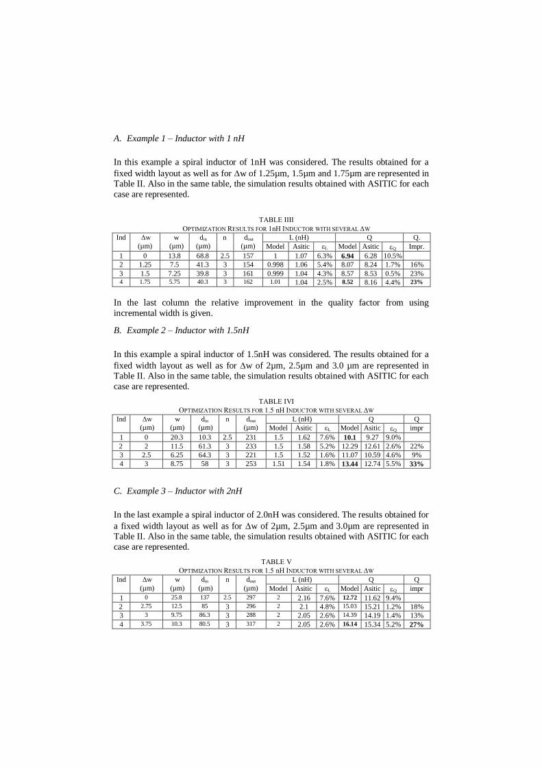
A. Example 1 – Inductor with 1 nH
In this example a spiral inductor of 1nH was considered. The results obtained for a
fixed width layout as well as for w of 1.25µm, 1.5µm and 1.75µm are represented in Table II. Also in the same table, the simulation results obtained with ASITIC for each
case are represented.
TABLE IIII
OPTIMIZATION RESULTS FOR 1nH INDUCTOR WITH SEVERAL W
Ind Δw
(µm)
w
(µm)
din
(µm)
n dout
(µm)
L (nH) Q Q.
Model Asitic εL Model Asitic Q Impr.
1 0 13.8 68.8 2.5 157 1 1.07 6.3% 6.94 6.28 10.5%
2 1.25 7.5 41.3 3 154 0.998 1.06 5.4% 8.07 8.24 1.7% 16%
3 1.5 7.25 39.8 3 161 0.999 1.04 4.3% 8.57 8.53 0.5% 23% 4 1.75 5.75 40.3 3 162 1.01 1.04 2.5% 8.52 8.16 4.4% 23%
In the last column the relative improvement in the quality factor from using
incremental width is given.
B. Example 2 – Inductor with 1.5nH
In this example a spiral inductor of 1.5nH was considered. The results obtained for a
fixed width layout as well as for w of 2µm, 2.5µm and 3.0 µm are represented in Table II. Also in the same table, the simulation results obtained with ASITIC for each
case are represented.
TABLE IVI
OPTIMIZATION RESULTS FOR 1.5 nH INDUCTOR WITH SEVERAL W
Ind Δw
(µm)
w
(µm)
din
(µm)
n dout
(µm)
L (nH) Q Q
Model Asitic εL Model Asitic Q impr
1 0 20.3 10.3 2.5 231 1.5 1.62 7.6% 10.1 9.27 9.0%
2 2 11.5 61.3 3 233 1.5 1.58 5.2% 12.29 12.61 2.6% 22%
3 2.5 6.25 64.3 3 221 1.5 1.52 1.6% 11.07 10.59 4.6% 9%
4 3 8.75 58 3 253 1.51 1.54 1.8% 13.44 12.74 5.5% 33%
C. Example 3 – Inductor with 2nH
In the last example a spiral inductor of 2.0nH was considered. The results obtained for
a fixed width layout as well as for w of 2µm, 2.5µm and 3.0µm are represented in Table II. Also in the same table, the simulation results obtained with ASITIC for each
case are represented.
TABLE V
OPTIMIZATION RESULTS FOR 1.5 nH INDUCTOR WITH SEVERAL W
Ind Δw
(µm)
w
(µm)
din
(µm)
n dout
(µm)
L (nH) Q Q
Model Asitic εL Model Asitic Q impr
1 0 25.8 137 2.5 297 2 2.16 7.6% 12.72 11.62 9.4%
2 2.75 12.5 85 3 296 2 2.1 4.8% 15.03 15.21 1.2% 18%
3 3 9.75 86.3 3 288 2 2.05 2.6% 14.39 14.19 1.4% 13%
4 3.75 10.3 80.5 3 317 2 2.05 2.6% 16.14 15.34 5.2% 27%
5 Conclusions
In this paper the analytical expressions for the evaluation of integrated inductor pi-
model parameters was proposed. This expressions consider variable width square
inductors, were each segment shows a constant increment of width. The validity of
the model was shown through three working examples considering the design of
1.0nH, 1.5nH and 2.0nH inductors at a working frequency of 1GHz. From the
examples presented a quality factor improvement in the order of 20% to 30% may be
obtained, by using variable width.
Should higher frequency of operation be envisaged, a more accurate inductor, such as
2-pi-model should be used. The adaptation of the proposed equations to the 2-pi-
model is under test.
References
1. I Krout, H. Mnif, M. Fakhfakh, and M. Loulou, “Optimizing LC VCO Performances Through a Heuristic”, Wseas Transactions on Electronics, vol. 5, pp.274-281, 2008.
2. P-W. Lai, L. Dobos, S. Long, “A 2.4GHz SiGe low phase noise VCO using on chip Tapped inductor”, Solid-State Circuits Conference - ESSCIRC,pp. 505–508, 2003.
3. L. L. K. Leung, and H. C. Luong, “A 1V9.7mW CMOS frequency synthesizer for IEEE 802.11a transceivers”, IEEE Trans. Microw. Theory Tech., vol. 56, pp. 39–48, Jan. 2008.
4. Wesley A. Gee, “CMOS Integrated LC Q-enhanced RF Filters for wireless Receivers”, PhD. Thesis, Georgia Institute of Technology, 2005.
5. C. Patrick Yue and S. Simon Wong, "Physical modeling of spiral inductors on silicon", IEEE Transactions on Electron Devices, Vol. 47 560-568, 2000.
6. Lai,I., Fujishima, M., ”Design and Modeling of Millimeter-Wave CMOS Circuits for Wireless Transceivers - Era of Sub-100nm Technology”, Springer, 2008.
7. Sunderarajan S. Mohan, Maria del Mar Hershenson, Stephen P. Boyd, and Thomas H. Lee, “Simple Accurate Expressions for Planar Spiral Inductances”, IEEE Journal of Solid-State Circuits, Vol. 34, Nº 10, October 1999.
8. S. Jenei, B. K. J. C. Nauwelaers, and S. Decoutere, “Physics-Based Closed-Form Inductance
Expression for Compact Modelling of Integrated Spiral Inductors,” IEEE J. Solid-State Circuits, vol. 37, no. 1, pp. 77–80, January 2002.
9. Y. S. Choi and J. B. Yoon, “Experimental Analysis of the Effect of Metal Thickness on the Quality Factor in Integrated Spiral Inductors for RF ICs,” IEEE Electron Device Lett., vol. 25, no. 2, pp. 76–79, February 2004.
10.D. J. Allstot, K. Choi, J. Park, “Parasitic-Aware Optimization of CMOS RF Circuits”, Kluwer Academic Publishers, ISBN 1-4020- 7399-2, 2003.
11.M. Park, C. H. Kim, C. S. Kim, et. al, “Frequency-Dependent Series Resistance of
Monolithic Spiral Inductors,” IEEEMicrowave Guided Lett., vol. 9, no. 12, pp. 514–516, December 1999.
12.Olive H. Murphy, “Advanced Physical Modelling of Multilayer Inductors for CMOS RF Front-End Applications”, PhD Thesis, University College Cork - National University of Ireland, October, 2005.
13. Pereira, P., Fino, M. H., Coito, F. & Ventim-Neves,M. “ADISI- An efficient tool for the automatic design of integrated spiral inductors” The 16th IEEE International Conference on Electronics, Circuits, and Systems (ICECS’09), 799–802, 2009.

70 APPENDIX A. PUBLICATIONS

75