an introduction to semiconductor detectors -...
TRANSCRIPT
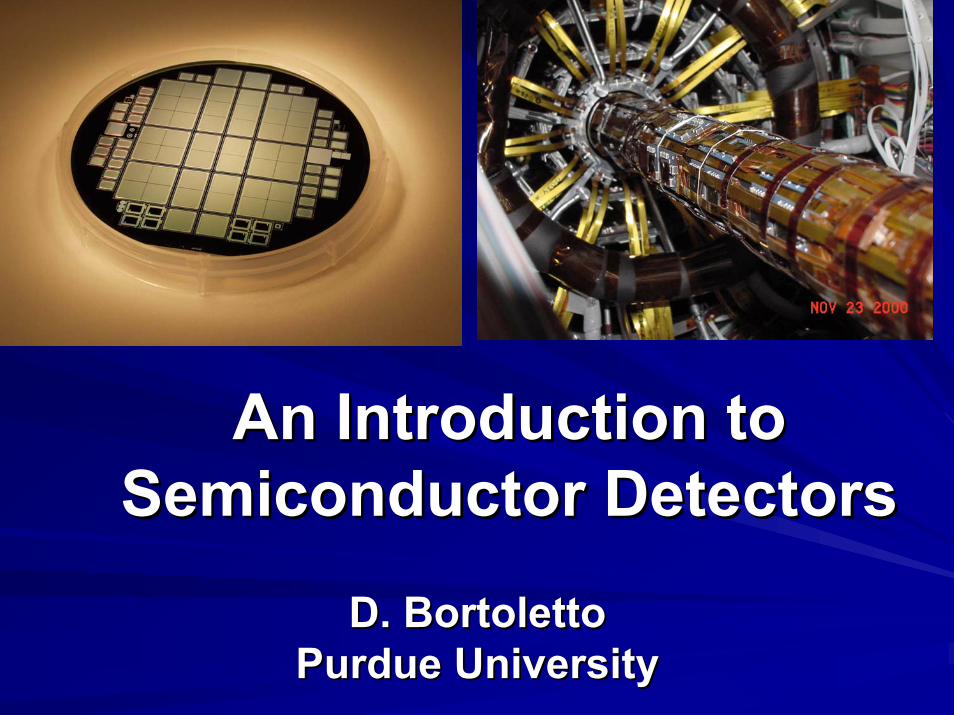
An Introduction to An Introduction to Semiconductor DetectorsSemiconductor Detectors
D. D. BortolettoBortolettoPurdue UniversityPurdue University
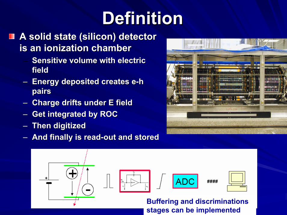
DefinitionDefinitionA solid state (silicon) detector A solid state (silicon) detector is an ionization chamberis an ionization chamber– Sensitive volume with electric Sensitive volume with electric
fieldfield–– Energy deposited creates Energy deposited creates ee--hh
pairspairs–– Charge drifts under E fieldCharge drifts under E field–– Get integrated by ROCGet integrated by ROC–– Then digitizedThen digitized–– And finally is readAnd finally is read--out and stored out and stored
Buffering and discriminations stages can be implemented
OutlineOutlineParticle detectionParticle detectionPrinciple of operation of solid state devicesPrinciple of operation of solid state devices–– The The pp--nn junctionjunction
ProcessingProcessingDetector design Detector design PerformancePerformanceRadiation DamageRadiation DamageElectronics and readoutElectronics and readoutAssembling DetectorsAssembling DetectorsTrends Trends –– RadRad hard sensorshard sensors–– Highly segmented detectorsHighly segmented detectors–– Large detectorsLarge detectors
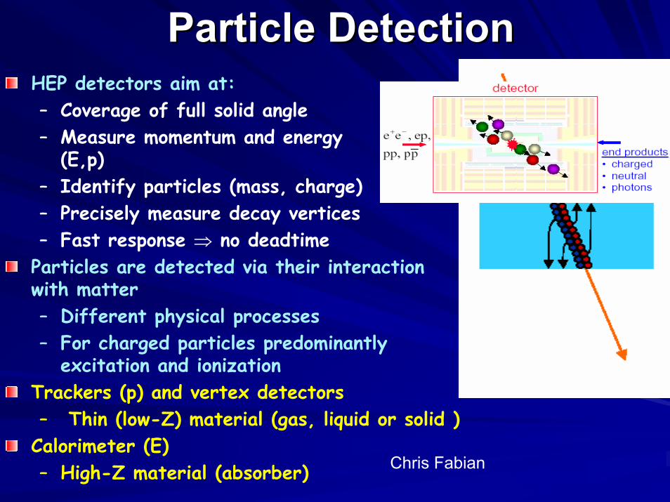
Particle DetectionParticle DetectionHEP detectors aim at:– Coverage of full solid angle– Measure momentum and energy
(E,p) – Identify particles (mass, charge)– Precisely measure decay vertices– Fast response ⇒ no deadtime
Particles are detected via their interaction with matter– Different physical processes– For charged particles predominantly
excitation and ionizationTrackers (p) and vertex detectors– Thin (low-Z) material (gas, liquid or solid )
Calorimeter (E)– High-Z material (absorber) Chris Fabian

Multipurpose Physics DetectorsMultipurpose Physics Detectors
p p
Tracking detector
Magnetic coilHadron calorimeterEM calorimeter
Muon ChambersB-Field
photons
electrons
quarks => jets
muons

Tracking and vertex detectors were crucial to the discovery of top: pp→tt→WbWb→lνlνbb. Vertex detection will be even more
important for searches of Higgs and SUSY at the LHC
Making DiscoveriesMaking Discoveriesb-jet b-jet
Missing energy
primary vertex
secondary vertex
~ 1 mm
“B-tagging”
CMUP muon
CMP muon

Solid State Detectors (SSD)Ionization chamber medium could be gas, liquid, or solid Ionization chamber medium could be gas, liquid, or solid –– Gas Gas ⇒⇒ electron and ion pairs; Semiconductor electron and ion pairs; Semiconductor ⇒⇒electron and hole pairselectron and hole pairs
GasGas SolidSolidDensityDensity LowLow HighHighAtomic number (Z)Atomic number (Z) LowLow Moderate Moderate (Z=14)Ionization Energy (Ionization Energy (εεII)) Moderate (Moderate (≈≈ 30 30 eVeV)) Low (Low (≈≈3.6 3.6 eVeV))Signal SpeedSignal Speed Moderate (10nsModerate (10ns--1010µµs)s) Fast (<20 ns)Fast (<20 ns)
Solid State DetectorsEnergy (E) to create e-h pairs 10 times smaller than gas ionization ⇒ increase charge⇒ good E resolution
IIENE
E εε
∝∝∝∆
/11
Greater density – Reduced range of secondary electron
⇒ excellent spatial resolution– Average Eloss ≈≈390eV/ 390eV/ µµm m ≈≈108 108 ee--hh/ /
µµm (charge collected is a function of m (charge collected is a function of thickness D but no multiplication)thickness D but no multiplication)
To minimize multiple scattering D should be small, 300 µµm m ≈≈32,000 32,000 ee--hh pairs yields pairs yields good S/Ngood S/N
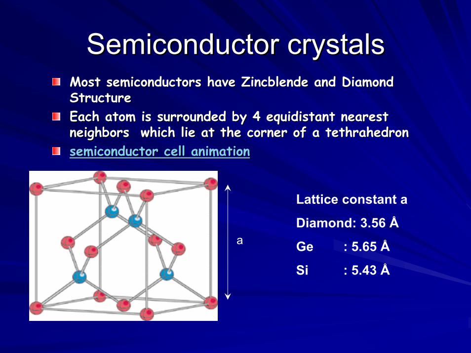
Semiconductor crystalsSemiconductor crystalsMost semiconductors have Most semiconductors have ZincblendeZincblende and Diamond and Diamond Structure Structure Each atom is surrounded by 4 equidistant nearest Each atom is surrounded by 4 equidistant nearest neighbors which lie at the corner of a neighbors which lie at the corner of a tethrahedrontethrahedronsemiconductor cell animationsemiconductor cell animation
Lattice constant a
Diamond: 3.56 Å
Ge : 5.65 Å
Si : 5.43 Å
a
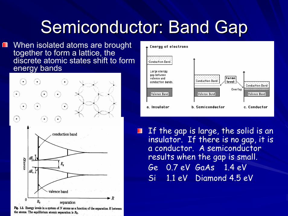
Semiconductor: Band GapSemiconductor: Band Gap
If the gap is large, the solid is an insulator. If there is no gap, it is a conductor. A semiconductor results when the gap is small. Ge 0.7 eV GaAs 1.4 eVSi 1.1 eV Diamond 4.5 eV
When isolated atoms are brought together to form a lattice, the discrete atomic states shift to form energy bands

SiliconSiliconExcellent detector materialExcellent detector material–– Low ionization energy (good signal). Low ionization energy (good signal). The
band gap is 1.1 eV, but it takes 3.6 eVto ionize an atom. The rest of the energy goes to phonon excitations (heat).
–– Long mean free path (good charge Long mean free path (good charge collection efficiency)collection efficiency)
–– High mobility (fast charge collection)High mobility (fast charge collection)–– Low Z (Z=14 low multiple scattering)Low Z (Z=14 low multiple scattering)
Oxide (SiOOxide (SiO22) has excellent electrical ) has excellent electrical propertiespropertiesGood mechanical propertiesGood mechanical properties–– Easily patterned to small dimensionsEasily patterned to small dimensions–– Can be operated in air and at room Can be operated in air and at room
temperature (many SSD require cooling)temperature (many SSD require cooling)Industrial experience and commercial Industrial experience and commercial applicationsapplicationsCrystalline⇒radiation damage
C. A. Klein, J. Applied Physics 39 (1968) 2029
E f
E
valence band
conductance band
h
e++
++
__
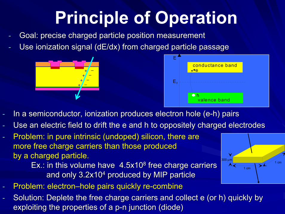
__
-- In a semiconductor, ionization produces electron hole (In a semiconductor, ionization produces electron hole (ee--hh) pairs) pairs-- Use an electric field to drift the e and h to oppositely chargedUse an electric field to drift the e and h to oppositely charged electrodeselectrodes-- Problem: in pure intrinsic (Problem: in pure intrinsic (undopedundoped) silicon, there are ) silicon, there are
more free charge carriers than those produced more free charge carriers than those produced by a charged particle.by a charged particle.
Ex.: in this volume have 4.5x10Ex.: in this volume have 4.5x1088 free charge carriersfree charge carriersand only 3.2x10and only 3.2x1044 produced by MIP particleproduced by MIP particle
-- Problem: electronProblem: electron––hole pairs quickly rehole pairs quickly re--combinecombine-- Solution: Deplete the free charge carriers and collect e (or h) Solution: Deplete the free charge carriers and collect e (or h) quickly by quickly by
exploiting the properties of a exploiting the properties of a pp--nn junction (diode)junction (diode)
300 µm
1 cm
1 cm
Principle of Operation-- Goal: precise charged particle position measurementGoal: precise charged particle position measurement-- Use ionization signal (Use ionization signal (dE/dxdE/dx) from charged particle passage) from charged particle passage
What Are Diodes Made Out Of?What Are Diodes Made Out Of?
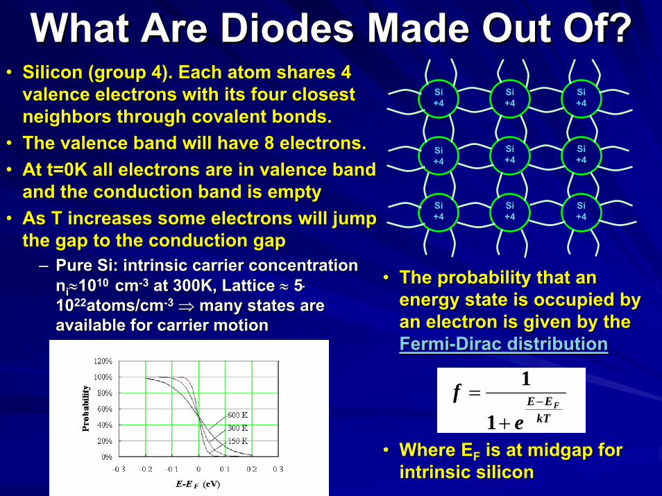
•• The probability that an The probability that an energy state is occupied by energy state is occupied by an electron is given by the an electron is given by the FermiFermi--DiracDirac distributiondistribution
•• Where EWhere EFF is at is at midgapmidgap for for intrinsic siliconintrinsic silicon
•• Silicon (group 4). Each atom shares 4 Silicon (group 4). Each atom shares 4 valence electrons with its four closest valence electrons with its four closest neighbors through covalent bonds. neighbors through covalent bonds.
•• The valence band will have 8 electrons.The valence band will have 8 electrons.•• At t=0K all electrons are in valence band At t=0K all electrons are in valence band
and the conduction band is emptyand the conduction band is empty•• As T increases some electrons will jump As T increases some electrons will jump
the gap to the conduction gapthe gap to the conduction gap–– Pure Pure SiSi: intrinsic carrier concentration : intrinsic carrier concentration
nnii≈≈101010 10 cmcm--33 at 300K, Lattice at 300K, Lattice ≈≈ 55⋅⋅10102222atoms/cmatoms/cm--33 ⇒⇒ many states are many states are available for carrier motionavailable for carrier motion
SiSi+4+4
SiSi+4+4
SiSi+4+4
Si Si +4+4
SiSi+4+4
SiSi+4+4
SiSi+4+4
SiSi+4+4
SiSi+4+4
kTEE F
ef −
+=
1
1

NN--Type MaterialType Material
+4+4+4+4
+5+5
+4+4
+4+4+4+4+4+4
+4+4+4+4
• In an n-type semiconductor, electron carriers are obtained by adding an atom with 5 valence electrons: arsenic, arsenic, antimony and phosphorusantimony and phosphorus
• Electrons are the majority carriers• Donors introduce energy levels 0.01 eV
below the conduction band ⇒ Fermi Level moves close to CB.
E f
E
V B
C Be
•• The 2D diagram shows the extra The 2D diagram shows the extra electron in nelectron in n--type materials. type materials.
•• This extra electron is loosely This extra electron is loosely bound bound
2
)()(Si
ii
atomElatticeEε
=
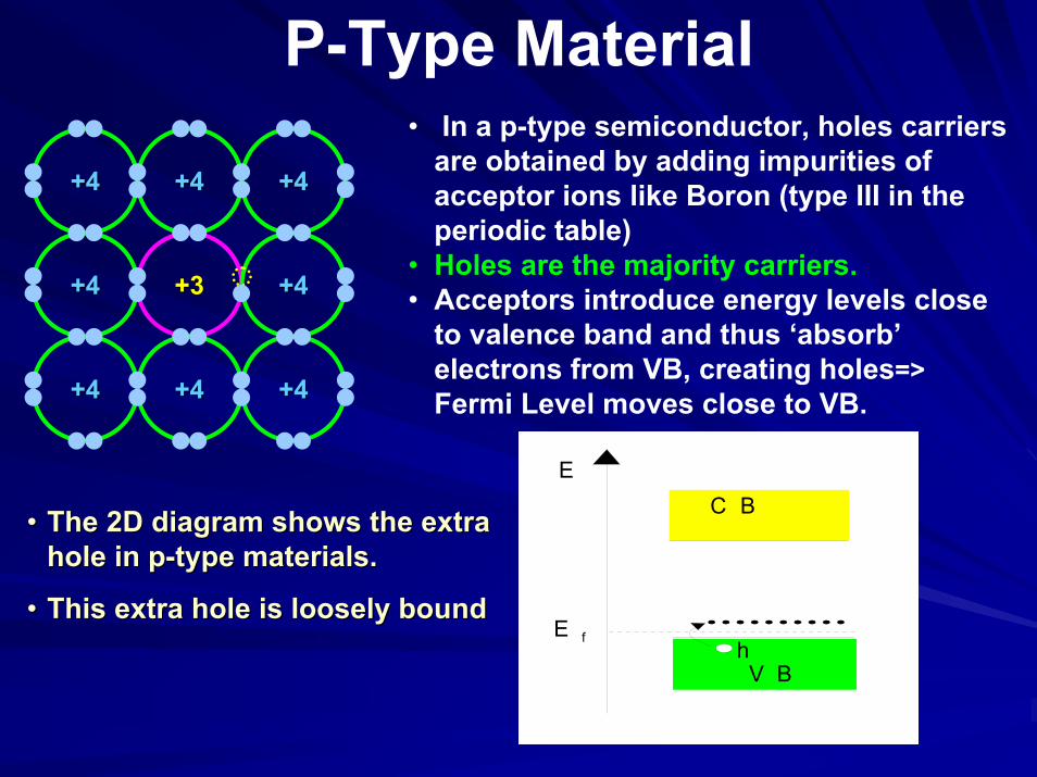
P-Type Material
+4+4+4+4
+3+3
+4+4
+4+4+4+4+4+4
+4+4+4+4
• In a p-type semiconductor, holes carriers are obtained by adding impurities of acceptor ions like Boron (type III in the periodic table)
• Holes are the majority carriers.• Acceptors introduce energy levels close
to valence band and thus ‘absorb’ electrons from VB, creating holes=> Fermi Level moves close to VB.
E f
E
V B
C B
h
•• The 2D diagram shows the extra The 2D diagram shows the extra hole in phole in p--type materials. type materials.
•• This extra hole is loosely bound This extra hole is loosely bound

The PN JunctionThe PN JunctionSpace Charge Region: When n and p type silicon are brought together⇒ gradient of electron and hole densities ⇒ migration of majority carriers across the junction which leaves a region of net charge of opposite sign on each side, called the space-charge region or depletion region (depleted of free charge carriers). The electric field in the region prevents further migration of carriers ⇒potential difference Φ=Vbi (built in potential).Junction: Interface where the p- and n-type materials meet.NA & ND: Negative and positive doping (n/cm3), usually ≈ 1015 –1020/cm3.p-n e-field
PP nn
-- -- -- -- --
-- -- -- -- --
-- -- -- -- --
-- -- -- -- --
+ + + + ++ + + + +
+ + + + ++ + + + +
+ + + + + + + + + +
+ + + + ++ + + + +
NaNa NdNdMetallurgical JunctionMetallurgical Junction
Space Charge Space Charge RegionRegionionized ionized
acceptorsacceptorsionized ionized donorsdonors
EE--FieldField
++++ __ __
h+ drifth+ drift h+ diffusionh+ diffusion ee-- diffusiondiffusion ee-- driftdrift== ==== ==
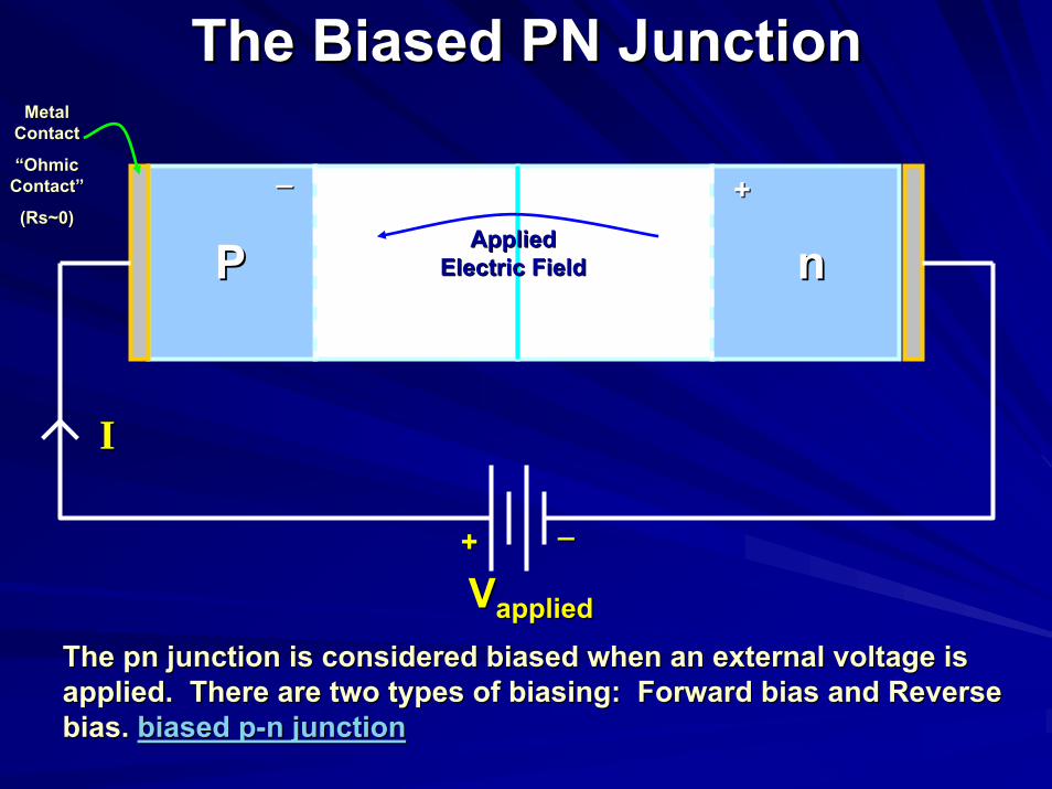
The Biased PN JunctionThe Biased PN JunctionMetal Metal
ContactContact
““OhmicOhmicContactContact””
(Rs~0)(Rs~0)
PP nn++__
Applied Applied Electric FieldElectric Field
++ __
VVappliedapplied
II
The The pnpn junction is considered biased when an external voltage is junction is considered biased when an external voltage is applied. There are two types of biasing: Forward bias and Reveapplied. There are two types of biasing: Forward bias and Reverse rse bias. bias. biased biased pp--nn junctionjunction

pn-Junction Overview
Dopant concentration
Carrier Density
Electric field
Electric potential
pp--type and ntype and n--type doped silicon type doped silicon forms a region depleted of free forms a region depleted of free charge carrierscharge carriersThe depleted region contains a The depleted region contains a nonnon--zero fixed charge and an zero fixed charge and an electric field. In the depletion electric field. In the depletion zone, electron zone, electron –– hole pairs do hole pairs do not recombine but drift along not recombine but drift along field lines field lines The depletion region can be The depletion region can be increased by applying a increased by applying a reversed bias voltagereversed bias voltage ⇒⇒allows allows charge collection from a larger charge collection from a larger volumevolume

Depletion regionDepletion depths for an abrupt p-n junction are found by solving Poisson eq. Note that charge conservation implies that NAdp=NDdn
If ND>>NA then the depletion region is wide on the n-side and shallow on the p-side (Ex. NA=1015cm-3, ND=5⋅1012 cm-3, dp=0.4 µm and dn=300 µm at Vbias=100 V)
The voltage needed to deplete the silicon thickness D is called the full depletion voltage Vfd. The E field is given by
)/1(12
)/1(12
ADD
biasn
DAA
biasp NNNq
VdNNNq
Vd+
=+
=εε
DVV
Dx
DV
xE fdbiasfd −+⎟
⎠⎞
⎜⎝⎛ −= 1
2)(
DAD
bias NNifNq
Vd >>=12ε
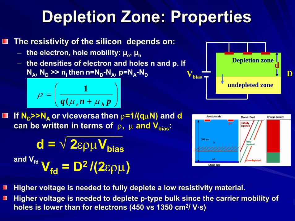
Depletion Zone: PropertiesDepletion Zone: PropertiesThe The resistivityresistivity of the silicon depends on: of the silicon depends on: – the electron, hole mobility: µe, µh
– the densities of electron and holes n and p. If NA, ND >> ni then n=ND-NA, p=NA-ND
If ND>>NA or viceversa then ρ=1/(qµN) and d can be written in terms of can be written in terms of ρ, , µµ and and VVbias::
and Vfd
–
+
Vbias
Depletion zone
undepleted zone
dD
⎟⎟⎠
⎞⎜⎜⎝
⎛+
=pnq he µµ
ρ(
1
Higher voltage is needed to fully deplete a low Higher voltage is needed to fully deplete a low resistivityresistivity material.material.Higher voltage is needed to deplete pHigher voltage is needed to deplete p--type bulk since the carrier mobility of type bulk since the carrier mobility of holes is lower than for electrons (450 holes is lower than for electrons (450 vsvs 1350 cm1350 cm22/ V/ V··s)s)
Vfd = D2 /(2ερµ)d = √ 2ερµVbias

Depletion Zone: PropertiesDepletion Zone: PropertiesThe depletion voltage can be determined by measuring the The depletion voltage can be determined by measuring the capacitance versus reverse bias voltage. The capacitance is simpcapacitance versus reverse bias voltage. The capacitance is simply ly the parallel plate capacity of the depletion zone. the parallel plate capacity of the depletion zone.
Vb
Depletion zone
undepleted zone
dDbV2
ACρµ
ε=
1/C2 vs voltage
Vfd
capacitance vs voltage

Diode I-V curve•• VVBB = Bias Voltage= Bias Voltage
•• IIDD = Current through = Current through Diode. IDiode. IDD is Negative for is Negative for Reverse Bias and Reverse Bias and Positive for Forward Positive for Forward BiasBias
•• IISS = Saturation Current = Saturation Current (leakage current)(leakage current)
•• VVBRBR = Breakdown = Breakdown VoltageVoltage
•• VVφφ = Barrier Potential = Barrier Potential Voltage which correspond Voltage which correspond the the ““built built ––inin”” voltagevoltage
VVBB
IIDD ((mAmA))
((nAnA))
VVBRBR
~V~Vφφ
IISS
2lni
ADbi n
NNq
kTV =

Leakage CurrentLeakage CurrentThe current in a reversedThe current in a reversed--biased diode biased diode is due to thermally generated minority is due to thermally generated minority carriers that can not recombine because carriers that can not recombine because of E field:of E field:–– Diffusion current: charge generated Diffusion current: charge generated
in the in the undepletedundepleted zone adjacent to zone adjacent to the depletion zone which diffuse into the depletion zone which diffuse into the depletion zone the depletion zone
–– Generation current Generation current JJgg, charge , charge generated in the depletion zone by generated in the depletion zone by defects or contaminantsdefects or contaminants
dnqJ ig
021
τ=
The intrinsic carrier density increases with temperature⇒ Ileak increases by a factor of 2 with a temperature increase of 8K
11 Guard Ring Diodes
1.E-10
1.E-09
1.E-08
1.E-070 500 1000
Reverse Bias Voltage (V)
Cur
rent
(A)
Diode 3Diode 4 Diode 11Diode 14Diode 20
Ileak sensitive to process quality
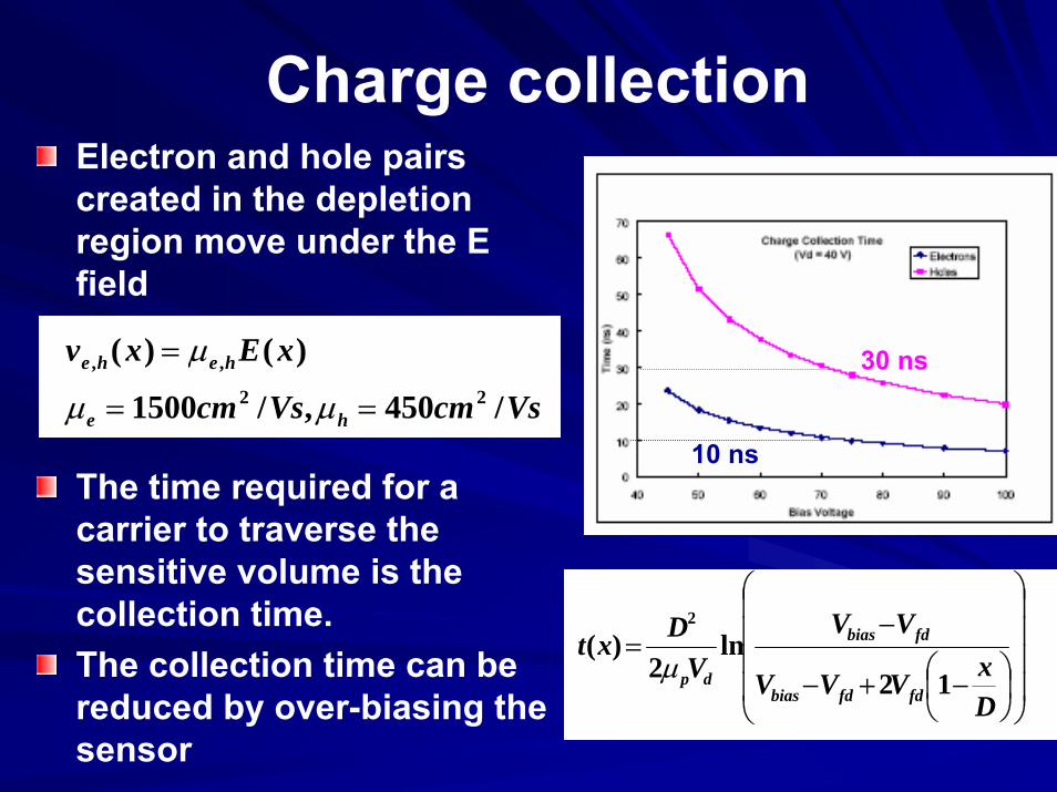
Charge collectionElectron and hole pairs created in the depletion region move under the E field
The time required for a carrier to traverse the sensitive volume is the collection time. The collection time can be reduced by over-biasing the sensor
VscmVscm
xExv
he
hehe
/450,/1500
)()(22
,,
==
=
µµ
µ
⎟⎟⎟⎟
⎠
⎞
⎜⎜⎜⎜
⎝
⎛
⎟⎠⎞
⎜⎝⎛ −+−
−=
DxVVV
VVV
Dxtfdfdbias
fdbias
dp 12ln
2)(
2
µ
10 ns
30 ns
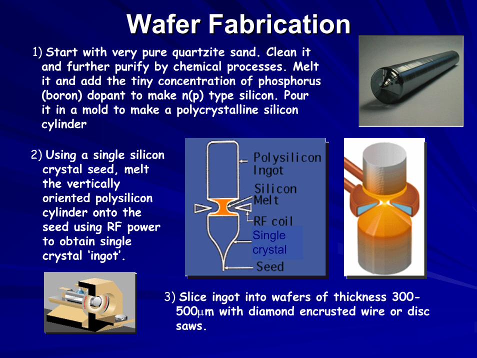
1) Start with very pure quartzite sand. Clean it and further purify by chemical processes. Melt it and add the tiny concentration of phosphorus (boron) dopant to make n(p) type silicon. Pour it in a mold to make a polycrystalline silicon cylinder
Wafer FabricationWafer Fabrication
Singlecrystal
2) Using a single silicon crystal seed, melt the vertically oriented polysiliconcylinder onto the seed using RF power to obtain single crystal ‘ingot’.
3) Slice ingot into wafers of thickness 300-500µm with diamond encrusted wire or disc saws.

Diode Processing Diode Processing animation
n-Si1) Start with n-doped silicon wafer, ρ ≈ 1-10 kΩcm. Silicon can be turned into n-type by neutron doping (30Si+n → 31Si, 31Si →31P+β-+ν)SiO
2Oxidation at 800 - 1200°C2)
Photolithography (= mask align + photo-resist layer + developing) followed by etching to make windows in oxide3)
UV light
maskPhoto-resist
etch

Diode ProcessingB
4) Doping by ion implantation (or by diffusion)
As
p+
n+
p+5) Annealing (healing of crystal lattice) at 600 °C
6) Photolithography followed by Al metallizationover implanted strips and over backplane usually by evaporation.
Al
⇒Simple DC-coupled silicon strip detector
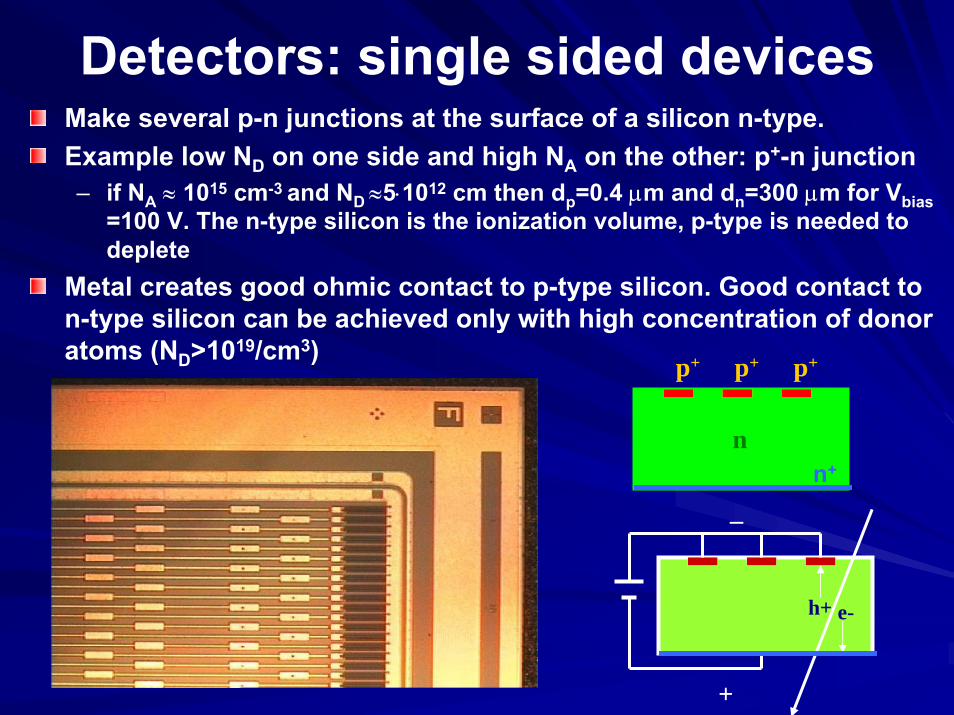
Detectors: single sided devicesMake several p-n junctions at the surface of a silicon n-type. Example low ND on one side and high NA on the other: p+-n junction – if NA ≈ 1015 cm-3 and ND ≈5⋅1012 cm then dp=0.4 µm and dn=300 µm for Vbias
=100 V. The n-type silicon is the ionization volume, p-type is needed to deplete
Metal creates good ohmic contact to p-type silicon. Good contact to n-type silicon can be achieved only with high concentration of donor atoms (ND>1019/cm3) p+p+ p+
nn+
+
–
h+ e-

Bias Resistor and AC CouplingBias Resistor and AC CouplingNeed to collect/measure charge Need to collect/measure charge on each strip on each strip ⇒⇒ high impedance high impedance bias connection (bias connection (≈≈1 M1 MΩΩ resistor) resistor) to isolate stripsto isolate stripsCouple input amplifier through a Couple input amplifier through a capacitor (AC coupling) to avoid capacitor (AC coupling) to avoid large DC input from leakage large DC input from leakage current.current.These structures are often These structures are often integrated on the silicon sensor. integrated on the silicon sensor. –– Bias resistors: deposition of doped Bias resistors: deposition of doped
polycrystalline silicon polycrystalline silicon –– Coupling capacitors: metal readout Coupling capacitors: metal readout
lines over the implants are lines over the implants are separated by an insulating dielectric separated by an insulating dielectric layer (SiOlayer (SiO2 2 , Si, Si33NN44). ).
+
–h+ e-
• Nice integration
• More masks
• Pin holes

Detectors: single sided devicesDetector design is usually made mask by mask (layer by layer) using CADENCE
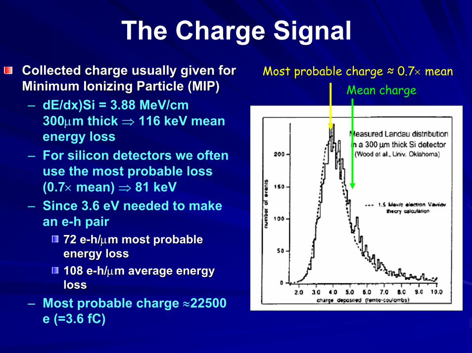
The Charge SignalCollected charge usually given for Collected charge usually given for Minimum Ionizing Particle (MIP) Minimum Ionizing Particle (MIP) – dE/dx)Si = 3.88 MeV/cm
300µm thick ⇒ 116 keV mean energy loss
– For silicon detectors we often use the most probable loss (0.7× mean) ⇒ 81 keV
– Since 3.6 eV needed to make an e-h pair
72 72 ee--h/h/µµmm most probable most probable energy lossenergy loss108 108 ee--h/h/µµmm average energy average energy lossloss
– Most probable charge ≈22500 e (=3.6 fC)
Mean chargeMost probable charge ≈ 0.7× mean

But There Is Noise …..But There Is Noise …..Landau distribution
with noise
noise distribution
ADC
Silicon sensors have low occupancy ⇒ most channels have no signal. Good hits are select by requiring NADC> noise tail. If cut is too high ⇒ efficiency loss Figure of Merit: Signal-to-Noise Ratio S/N. Typical Values > 10-15, people get nervous below 10. Radiation damage severely degrades the S/N. Thus S/N determines lifetime of the detector in a harsh radiation environment
Landau distribution has a low energy tail which broadens because of noise. – Noise sources:
Capacitance ENC ∝ Cd
Leakage Current ENC ∝ √ IThermal Noise ENC ∝ √( kT/R)
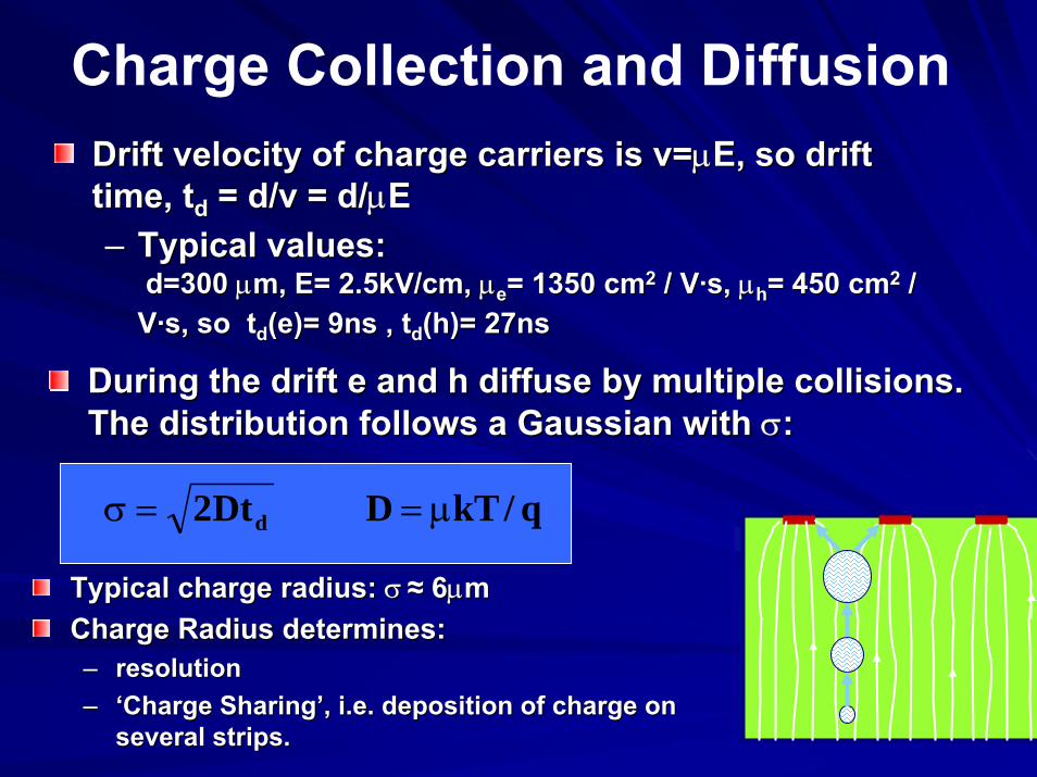
Charge Collection and DiffusionDrift velocity of charge carriers is v=Drift velocity of charge carriers is v=µµE, so drift E, so drift time, ttime, tdd = d/v = d/= d/v = d/µµEE–– Typical values:Typical values:
d=300 d=300 µµm, E= 2.5kV/cm, m, E= 2.5kV/cm, µµee= 1350 cm= 1350 cm22 / V/ V··s, s, µµhh= 450 cm= 450 cm22 / / VV··s, so ts, so tdd(e)= 9ns , t(e)= 9ns , tdd(h)= 27ns(h)= 27ns
During the drift e and h diffuse by multiple collisions. During the drift e and h diffuse by multiple collisions. The distribution follows a Gaussian with The distribution follows a Gaussian with σσ::
Typical charge radius: Typical charge radius: σσ ≈≈ 66µµmmCharge Radius determines:Charge Radius determines:–– resolutionresolution–– ‘‘Charge SharingCharge Sharing’’, i.e. deposition of charge on , i.e. deposition of charge on
several strips.several strips.
q/kTDDt2 d µ==σ

Double Sided DetectorsWhy not get a 2nd coordinate by measuring the position of the (electron) charge collected on the opposite face?Problem: Problem: –– nn--strips are not isolated because of an strips are not isolated because of an
electron accumulation layer at the Sielectron accumulation layer at the Si--SiOSiO22interface. This effect is due to the interface. This effect is due to the presence of positive charge in SiOpresence of positive charge in SiO22 layer layer which attracts electrons.which attracts electrons.
SOLUTION– p-strips in between the n-strips.– Put “field plates” (metal over oxide) over
the n-strips and apply a potential on the plates to repel the electrons.
pp p
n
p+p+ p+
n+ n+ n+n-bulk
n+ n+ n+n-bulk
p+ p+
n+ n+ n+n-bulk
+ + +
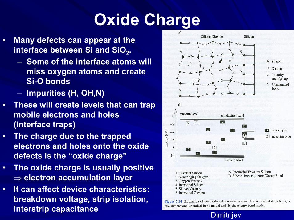
Oxide Charge• Many defects can appear at the
interface between Si and SiO2. – Some of the interface atoms will
miss oxygen atoms and create Si-O bonds
– Impurities (H, OH,N)• These will create levels that can trap
mobile electrons and holes (Interface traps)
• The charge due to the trapped electrons and holes onto the oxide defects is the “oxide charge”
• The oxide charge is usually positive ⇒ electron accumulation layer
• It can affect device characteristics: breakdown voltage, strip isolation, interstrip capacitance
Dimitrijev
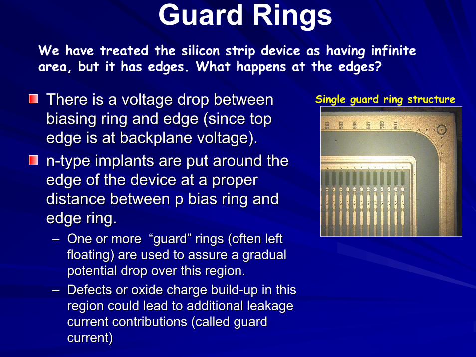
Guard RingsWe have treated the silicon strip device as having infinite area, but it has edges. What happens at the edges?
There is a voltage drop between There is a voltage drop between biasing ring and edge (since top biasing ring and edge (since top edge is at backplane voltage). edge is at backplane voltage). nn--type implants are put around the type implants are put around the edge of the device at a proper edge of the device at a proper distance between p bias ring and distance between p bias ring and edge ring. edge ring. –– One or more One or more ““guardguard”” rings (often left rings (often left
floating) are used to assure a gradual floating) are used to assure a gradual potential drop over this region.potential drop over this region.
–– Defects or oxide charge buildDefects or oxide charge build--up in this up in this region could lead to additional leakage region could lead to additional leakage current contributions (called guard current contributions (called guard
Single guard ring structure
current)current)
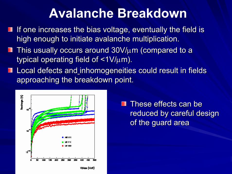
If one increases the bias voltage, eventually the field is If one increases the bias voltage, eventually the field is high enough to initiate avalanche multiplication.high enough to initiate avalanche multiplication.This usually occurs around 30V/This usually occurs around 30V/µµm (compared to a m (compared to a typical operating field of <1V/typical operating field of <1V/µµm). m). Local defects andLocal defects and inhomogeneitiesinhomogeneities could result in fields could result in fields approaching the breakdown point. approaching the breakdown point.
Avalanche Breakdown
These effects can be These effects can be reduced by careful design reduced by careful design of the guard areaof the guard area

Breakdown and Guard ringsOperation of silicon sensors at high depletion voltage Operation of silicon sensors at high depletion voltage without breakdown can be achieved using multiple guard without breakdown can be achieved using multiple guard rings.rings.
6 Guard Ring Diodes
1.E-11
1.E-10
1.E-09
1.E-08
0 200 400 600Reverse Bias (V)
Cur
rent
(A) Diode 2
Diode 3Diode 4Diode 8
11 Guard Ring Diodes
1.E-10
1.E-09
1.E-08
1.E-070 500 1000
Reverse Bias Voltage (V)
Cur
rent
(A)
Diode 3Diode 4 Diode 11Diode 14Diode 20
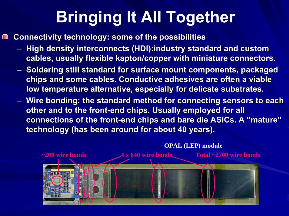
Bringing It All TogetherConnectivity technology: some of the possibilitiesConnectivity technology: some of the possibilities–– High density interconnects (HDI):industry standard and custom High density interconnects (HDI):industry standard and custom
cables, usually flexible cables, usually flexible kaptonkapton/copper with miniature connectors./copper with miniature connectors.–– Soldering still standard for surface mount components, packaged Soldering still standard for surface mount components, packaged
chips and some cables. Conductive adhesives are often a viable chips and some cables. Conductive adhesives are often a viable low temperature alternative, especially for delicate substrates.low temperature alternative, especially for delicate substrates.
–– Wire bonding: the standard method for connecting sensors to eachWire bonding: the standard method for connecting sensors to eachother and to the frontother and to the front--end chips. Usually employed for all end chips. Usually employed for all connections of the frontconnections of the front--end chips and bare die end chips and bare die ASICsASICs. A “mature” . A “mature” technology (has been around for about 40 years).technology (has been around for about 40 years).
4 x 640 wire bonds~200 wire bonds Total ~2700 wire bondsOPAL (LEP) module

Wire BondingWire Bonding•• Ultrasonic power is used to vibrate needleUltrasonic power is used to vibrate needle--
like tool on top of Al wire. Friction welds like tool on top of Al wire. Friction welds wire to wire to metallizedmetallized substrate underneath.substrate underneath.
•• Pitch: 80Pitch: 80µµm pitch in a single row and 40m pitch in a single row and 40µµm m in two staggered rows (typical FE chip pitch in two staggered rows (typical FE chip pitch is is ≈≈4444µµm).m).
•• ≈≈2525µµm diameter aluminum wire and bond to m diameter aluminum wire and bond to aluminum pads (chips) or gold pads (hybrid aluminum pads (chips) or gold pads (hybrid substrates).substrates).
•• Used in industry (PC processors) but not Used in industry (PC processors) but not with such thin wire or small pitch.with such thin wire or small pitch.
View through microscope of wire bonds connecting sensor to fan-
out circuit
Electron micrograph of bond “foot”
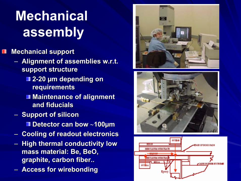
Mechanical supportMechanical support–– Alignment of assemblies Alignment of assemblies w.r.tw.r.t. .
support structure support structure 22--20 20 µµm depending on m depending on requirementsrequirementsMaintenance of alignment Maintenance of alignment and and fiducialsfiducials
–– Support of siliconSupport of siliconDetector can bow Detector can bow ∼∼100100µµmm
–– Cooling of readout electronicsCooling of readout electronics–– High thermal conductivity low High thermal conductivity low
mass material: Be, mass material: Be, BeOBeO, , graphite, carbon fiber..graphite, carbon fiber..
–– Access for Access for wirebondingwirebonding
Mechanical assembly
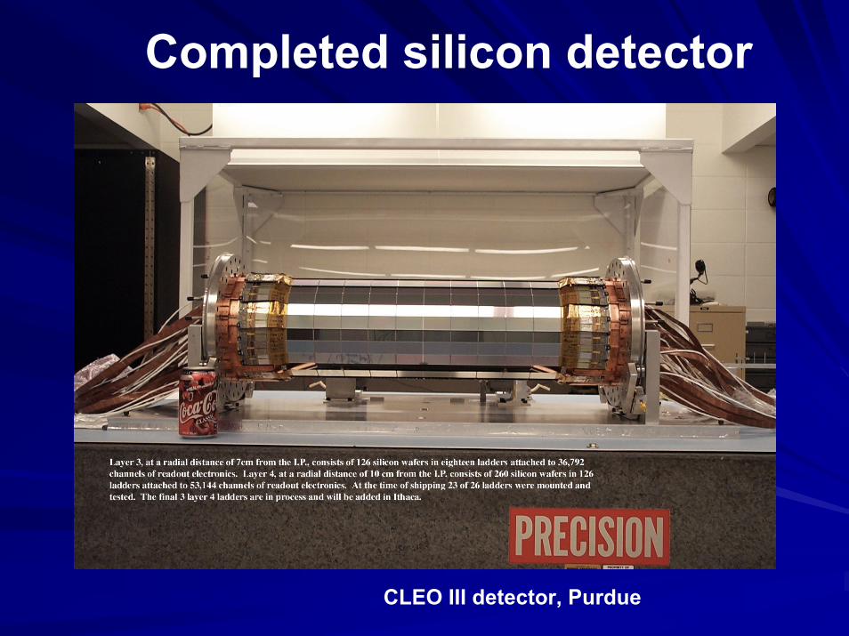
Completed silicon detector
CLEO III detector, Purdue
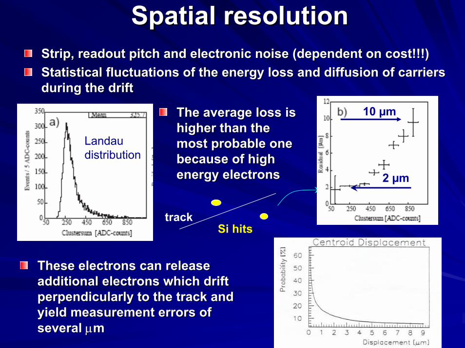
The average loss is The average loss is higher than the higher than the most probable one most probable one because of high because of high energy electronsenergy electrons
Spatial resolutionSpatial resolutionStrip, readout pitch and electronic noise (dependent on cost!!!)Strip, readout pitch and electronic noise (dependent on cost!!!)Statistical fluctuations of the energy loss and diffusion of carStatistical fluctuations of the energy loss and diffusion of carriers riers during the driftduring the drift
These electrons can release These electrons can release additional electrons which drift additional electrons which drift perpendicularly to the track and perpendicularly to the track and yield measurement errors of yield measurement errors of several several µµm m
Landau distribution
trackSi hits
10 µm
2 µm
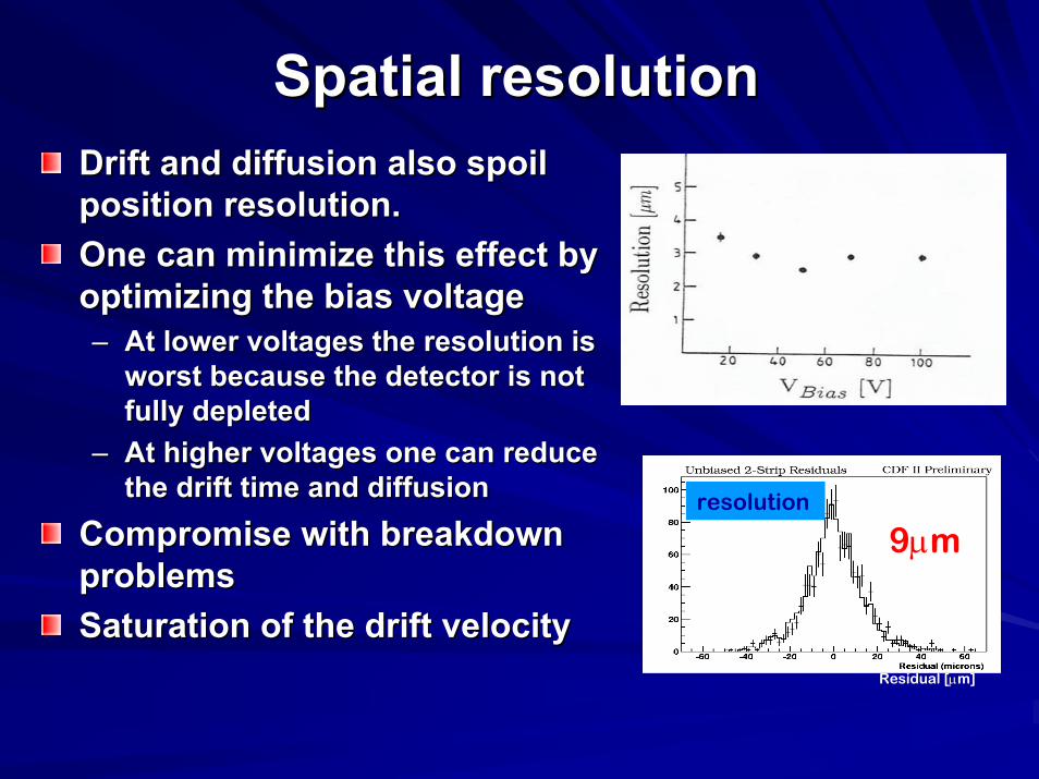
Spatial resolutionSpatial resolutionDrift and diffusion also spoil Drift and diffusion also spoil position resolution.position resolution.One can minimize this effect by One can minimize this effect by optimizing the bias voltageoptimizing the bias voltage–– At lower voltages the resolution is At lower voltages the resolution is
worst because the detector is not worst because the detector is not fully depletedfully depleted
–– At higher voltages one can reduce At higher voltages one can reduce the drift time and diffusionthe drift time and diffusion
Compromise with breakdown Compromise with breakdown problemsproblemsSaturation of the drift velocitySaturation of the drift velocity
resolution
9µm
Residual [µm]
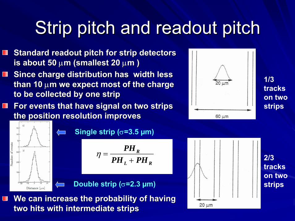
Standard readout pitch for strip detectors Standard readout pitch for strip detectors is about 50 is about 50 µµm (smallest 20 m (smallest 20 µµm )m )Since charge distribution has width less Since charge distribution has width less than 10 than 10 µµm we expect most of the charge m we expect most of the charge to be collected by one stripto be collected by one stripFor events that have signal on two strips For events that have signal on two strips the position resolution improvesthe position resolution improves
We can increase the probability of having We can increase the probability of having two hits with intermediate stripstwo hits with intermediate strips
Strip pitch and readout pitchStrip pitch and readout pitch
RL
R
PHPHPH
+=η
1/3 tracks on two strips
2/3 tracks on two strips
Single strip (σ=3.5 µm)
Double strip (σ=2.3 µm)
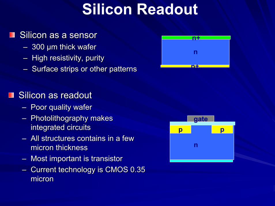
Silicon Readout Silicon as a sensorSilicon as a sensor–– 300 300 µµm thick waferm thick wafer–– High High resistivityresistivity, purity, purity–– Surface strips or other patternsSurface strips or other patterns
n
p+
n+
Silicon as readoutSilicon as readout–– Poor quality waferPoor quality wafer–– Photolithography Photolithography makes makes
integrated circuitsintegrated circuits–– All structures contains in a few All structures contains in a few
micron thicknessmicron thickness–– Most important is transistorMost important is transistor–– Current technology is CMOS 0.35 Current technology is CMOS 0.35
micronmicron
n
p pgate
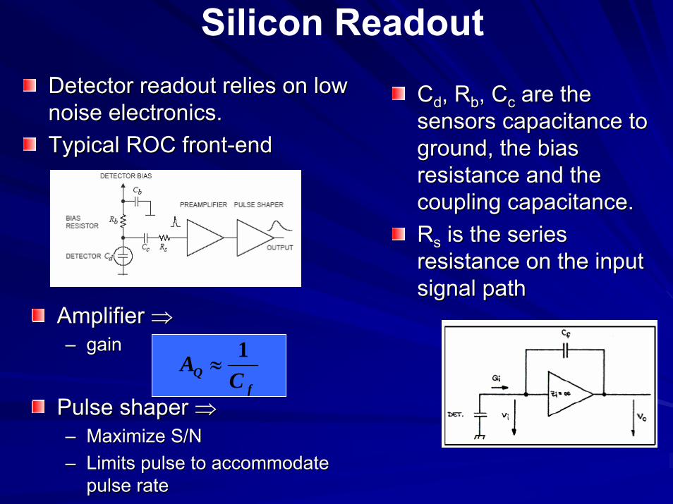
Silicon Readout Detector readout relies on low Detector readout relies on low noise electronics. noise electronics. Typical ROC frontTypical ROC front--endend
CCdd, , RRbb, C, Ccc are the are the sensors capacitance to sensors capacitance to ground, the bias ground, the bias resistance and the resistance and the coupling capacitance.coupling capacitance.RRss is the series is the series resistance on the input resistance on the input signal pathsignal path
Amplifier Amplifier ⇒⇒–– gaingain
Pulse shaper Pulse shaper ⇒⇒–– Maximize S/N Maximize S/N –– Limits pulse to accommodate Limits pulse to accommodate
pulse ratepulse rate
fQ C
A 1≈
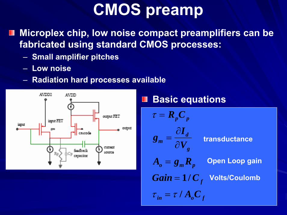
CMOS preampMicroplex chip, low noise compact preamplifiers can be fabricated using standard CMOS processes:– Small amplifier pitches– Low noise– Radiation hard processes available
Basic equations
foin
f
pmo
g
dm
pp
CA
CGain
RgA
VIg
CR
/
/1
ττ
τ
=
=
=
∂∂
=
=
transductance
Open Loop gain
Volts/Coulomb
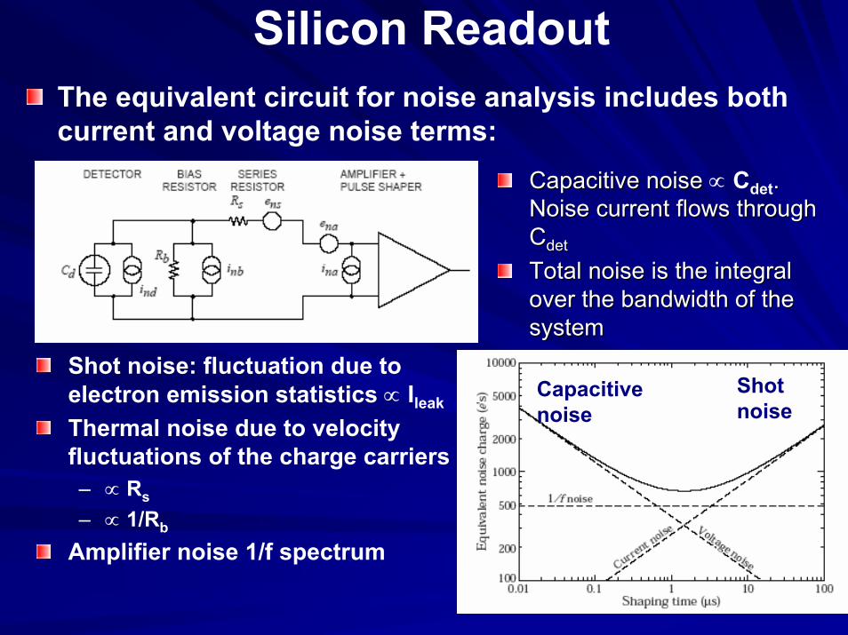
Silicon Readout The equivalent circuit for noise analysis includes both current and voltage noise terms:
Shot noise: fluctuation due to electron emission statistics ∝ Ileak
Thermal noise due to velocity fluctuations of the charge carriers– ∝ Rs
– ∝ 1/Rb
Amplifier noise 1/f spectrum
Capacitive noise Capacitive noise ∝ Cdet. . Noise current flows through Noise current flows through CCdetdet
Total noise is the integral Total noise is the integral over the bandwidth of the over the bandwidth of the systemsystem
Shot noise
Capacitive noise
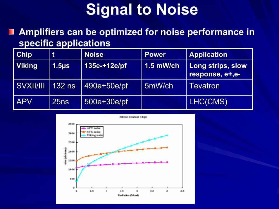
Amplifiers can be optimized for noise performance in specific applications
Signal to Noise
ChipChip tt NoiseNoise PowerPower ApplicationApplicationVikingViking 1.51.5µµss 135e135e--+12e/pf+12e/pf 1.5 1.5 mW/chmW/ch Long strips, slow Long strips, slow
response, response, e+,ee+,e--
SVXII/IIISVXII/III 132 ns132 ns 490e+50e/pf490e+50e/pf 5mW/ch5mW/ch TevatronTevatron
APVAPV 25ns25ns 500e+30e/pf500e+30e/pf LHC(CMS)LHC(CMS)
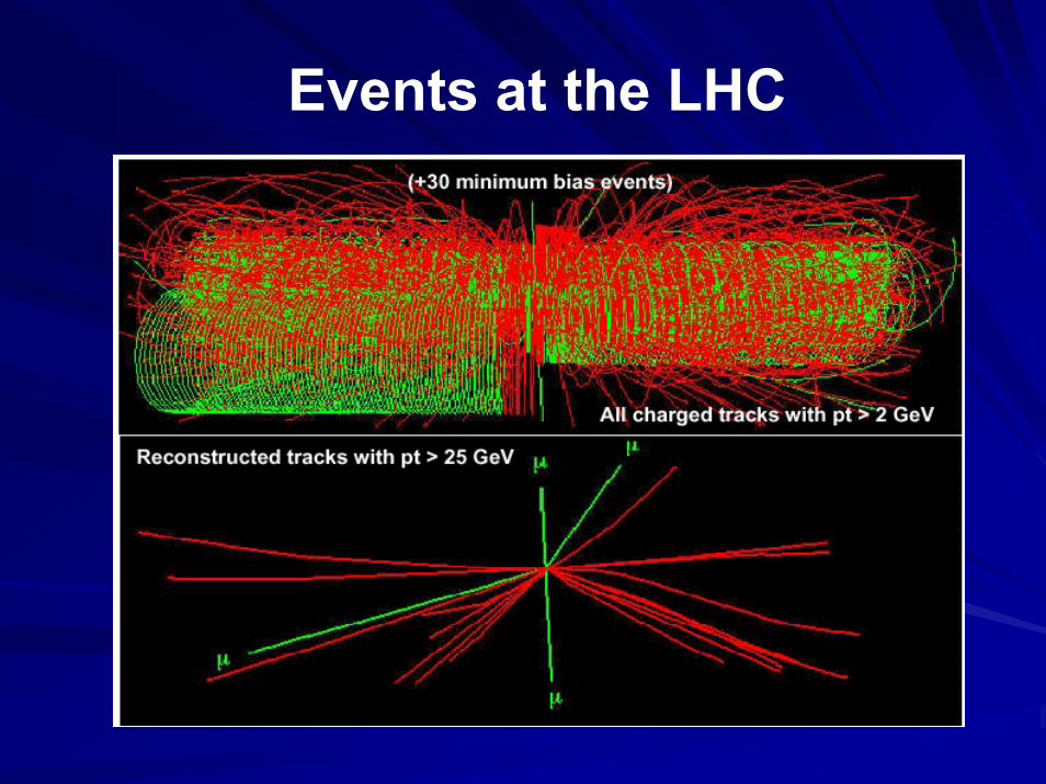
Events at the LHC
Radiation Damage in SiliconRadiation Damage in SiliconTwo general types of radiation damageTwo general types of radiation damage–– “Bulk” damage“Bulk” damage due to physical impact within the crystaldue to physical impact within the crystal–– “Surface” damage“Surface” damage in the oxide or Si/SiOin the oxide or Si/SiO22 interfaceinterface
Cumulative effectsCumulative effects–– Increased leakage current (increased shot noise)Increased leakage current (increased shot noise)–– Silicon bulk type inversion (nSilicon bulk type inversion (n--type to ptype to p--type)type)–– Increased depletion voltageIncreased depletion voltage–– Increased capacitanceIncreased capacitance
Sensors can fail from radiation damageSensors can fail from radiation damage–– Noise too high to effectively operate Noise too high to effectively operate –– Depletion voltage too high to depleteDepletion voltage too high to deplete–– Loss of interLoss of inter--strip isolation (charge spreading) strip isolation (charge spreading)
Signal/noise ratio is the quantity to watchSignal/noise ratio is the quantity to watch

Surface Damage+++++
+++ ++
Surface DamageSurface damage generation:Surface damage generation:–– Ionizing radiation creates electronIonizing radiation creates electron--hole pairs in hole pairs in
the SiOthe SiO22
–– Many recombine, electrons migrate quicklyMany recombine, electrons migrate quickly–– Holes slowly migrate to Si/SiOHoles slowly migrate to Si/SiO22 interface sinceinterface since
hole mobility is much lower than for electrons hole mobility is much lower than for electrons (20 cm(20 cm22/Vs vs. 2x10/Vs vs. 2x1055 cmcm22/Vs) /Vs)
–– Some holes ‘stick’ in the boundary layerSome holes ‘stick’ in the boundary layerSurface damage results in Surface damage results in –– Increased interface trapped charge Increased interface trapped charge –– Increased fixed oxide chargesIncreased fixed oxide charges–– Surface generation centersSurface generation centers
Metal (Al)Oxide (SiO2)
Semiconductor (Si)
-- ---
-- -
-++
+
+
+
--- -
--
++ -
+
+
++ +
+
+
+ +
+ + + +
+
After electrontransport:
After transportof the holes:
MOS devices are sensitive to surface damage– Electron accumulation under the oxide interface can alter the depletion
voltage (depends on oxide quality and sensor geometry)– In silicon strip sensors, surface damage effects (oxide charge) saturate at a
few hundred kRad
Interface (SiOx)

Surface Damage EffectsSurface Damage EffectsCharges in the oxide layer can cause:Charges in the oxide layer can cause:–– Risk to readout electronicsRisk to readout electronics
threshold shifts noise and gain deterioration
–– Increase in the sensors capacitancesIncrease in the sensors capacitances–– Single event upset in small feature size Single event upset in small feature size
devicesdevicesProblems can be minimized by:Problems can be minimized by:–– Silicon crystal orientation (<100> Silicon crystal orientation (<100>
rather than <111>) can minimize rather than <111>) can minimize interface traps at boundaryinterface traps at boundary
–– Reducing oxide thicknessReducing oxide thicknessVoltage shifts are proportional to Voltage shifts are proportional to the square of the thickness (0.25 the square of the thickness (0.25 µµm m CMOS more CMOS more radrad hard)hard)
–– ProcessingProcessing
02468
10
RM
S N
oise
on
Ped
esta
l02468
10
02468
10
0 200 400 600 800 1000 1200Channel Number
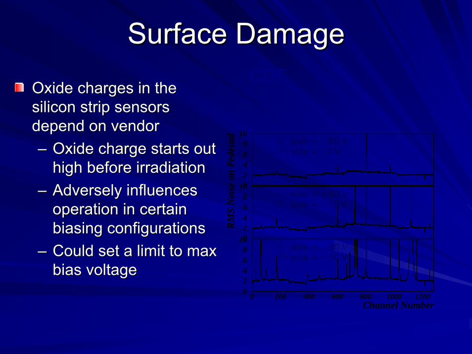
Surface DamageSurface DamageCDF
Oxide charges in the Oxide charges in the silicon strip sensors silicon strip sensors depend on vendordepend on vendor–– Oxide charge starts out Oxide charge starts out
high before irradiation high before irradiation –– Adversely influences Adversely influences
operation in certain operation in certain biasing configurationsbiasing configurations
–– Could set a limit to max Could set a limit to max bias voltagebias voltage

Process Defects and ScratchesProcess Defects and Scratches

Bulk DamageBulk Damage
O
P
Vacancy
Disordered region
Di-vacancy
Interstitial
C
Vacancy/OxygenCenter
CarbonInterstitial
CC
Phosphorous dopant
Carbon-CarbonPair
C O
Carbon-Oxygen pair
Bulk damage is mainly from Bulk damage is mainly from hadrons displacing primary lattice hadrons displacing primary lattice atoms (for E > 25 atoms (for E > 25 eVeV))–– Results in silicon interstitial, Results in silicon interstitial,
vacancy, and large disordered vacancy, and large disordered regionregion
–– 1 1 MeVMeV neutron transfers 60neutron transfers 60--70 70 keVkeVto recoiling silicon atom, which in to recoiling silicon atom, which in turn displaces ~1000 additional turn displaces ~1000 additional atomsatoms
Defects can recombine or migrate Defects can recombine or migrate through the lattice to form more through the lattice to form more complex and stable defectscomplex and stable defects–– Annealing can be beneficial Annealing can be beneficial –– Defects can be stable or unstableDefects can be stable or unstable–– Displacement damage is directly Displacement damage is directly
related to the nonrelated to the non--ionizing energy ionizing energy loss (NIEL) of the interactionloss (NIEL) of the interaction
–– Varies by incident particle type Varies by incident particle type and energyand energy

charged particle multiplicity
Bulk DamageBulk DamageDisplacement damage Displacement damage occurs for all particlesoccurs for all particles–– PionsPions and neutrons are and neutrons are
typically the most typically the most numerousnumerous
Particle flux in a collider Particle flux in a collider environmentenvironment–– Experience from CDF Run Experience from CDF Run
I suggests I suggests ΦΦ = = ΦΦ00/r/r1.71.7
–– Neutron flux falls less Neutron flux falls less rapidly; it eventually rapidly; it eventually becomes significantbecomes significant
NIEL Radiation damage NIEL Radiation damage studies typically normalized studies typically normalized to 1 to 1 MeVMeV neutron damage neutron damage equivalentequivalent

Bulk Damage EffectsBulk Damage EffectsLeakage Current: Leakage Current:
∆∆II = α= α(t)(t)ΦΦVV–– αα(t(t) (damage constant), V (volume), ) (damage constant), V (volume),
and and ΦΦ ((fluencefluence).).–– Annealing reduces the currentAnnealing reduces the current–– Independent of particle typeIndependent of particle type
Depletion Voltage:Depletion Voltage:VVdepdep = q|N= q|Neffeff|d|d22/2/2εεεε00
–– Effective Effective dopantdopant concentration concentration (N(Neff eff = = NNdonorsdonors –– NNacceptorsacceptors), sensor ), sensor thickness (d), thickness (d), permitivitypermitivity ((εεεε00).).
–– Depletion voltage is parameterized Depletion voltage is parameterized in three parts:in three parts:
Short term annealing (NShort term annealing (Naa))A stable component (A stable component (NNcc))Long term reverse annealing (NLong term reverse annealing (NYY)
Before Irradiation:
)
P N
P NSmall difference: small depletion V
Small area: small current
Conc
ent r
ation
(log
sca le)
After Irradiation:
Large area: large current
Large difference: Large depletion V
Conc
ent r
ation
(log
sca le)

Leakage CurrentLeakage CurrentDefects create intermediate Defects create intermediate states within the band gapstates within the band gap–– intermediate states act as intermediate states act as
‘stepping stones’ of thermal ‘stepping stones’ of thermal generation of electron/hole generation of electron/hole pairspairs
–– Some of these states anneal Some of these states anneal away; the bulk current reduces away; the bulk current reduces with time (and temperature) with time (and temperature) after irradiation after irradiation
Annealing function Annealing function αα(t)(t)–– Parameterized by the sum of several Parameterized by the sum of several
exponentials exponentials ααiiexp(exp(--t/t/ττii))–– Full annealing (for the example below) Full annealing (for the example below)
reached after ~1 year at 20ºCreached after ~1 year at 20ºC–– At low temperatures, annealing At low temperatures, annealing
effectively stopseffectively stops–– Dependant on incident particle type (?)Dependant on incident particle type (?)

Fig. 7.: Fluence dependence of leakage current for detectors produced by various process technologies from different silicon materials. The current was measured after a heat treatment for
80 min at 60°C [14].
Fig.8: Current related damage rate α as function of cumulated annealing time at 60°C. Comparison between data obtained for oxygen diffused silicon and parameterisation given in Ref. [14].
Leakage CurrentLeakage CurrentMeasured values of Measured values of αα(t)(t)–– One quotes measured values of One quotes measured values of
αα(t) after complete annealing at (t) after complete annealing at T=20ºC: T=20ºC: αα∞∞ = = αα(t=∞)(t=∞)
–– ‘World averages’ for ‘World averages’ for αα∞∞ are :are :2.2 x 102.2 x 10--1717 A/cmA/cm33 for protons, for protons, pionspions2.9 x 102.9 x 10--1717 A/cmA/cm33 for neutronsfor neutrons
–– Recent results show Recent results show αα(t(t=80min,T=60ºC)= 4.0 x 10=80min,T=60ºC)= 4.0 x 10--1717
A/cmA/cm33 for all types of silicon, levels for all types of silicon, levels of impurities, and incident particle of impurities, and incident particle types (NIM A426 (1999)86).types (NIM A426 (1999)86).
1011 1012 1013 1014 1015
Φeq [cm-2]10-6
10-5
10-4
10-3
10-2
10-1
∆I /
V
[A/c
m3 ]
n-type FZ - 7 to 25 KΩcmn-type FZ - 7 to 25 KΩcmn-type FZ - 7 KΩcmn-type FZ - 7 KΩcmn-type FZ - 4 KΩcmn-type FZ - 4 KΩcmn-type FZ - 3 KΩcmn-type FZ - 3 KΩcm
n-type FZ - 780 Ωcmn-type FZ - 780 Ωcmn-type FZ - 410 Ωcmn-type FZ - 410 Ωcmn-type FZ - 130 Ωcmn-type FZ - 130 Ωcmn-type FZ - 110 Ωcmn-type FZ - 110 Ωcmn-type CZ - 140 Ωcmn-type CZ - 140 Ωcm
p-type EPI - 2 and 4 KΩcmp-type EPI - 2 and 4 KΩcm
p-type EPI - 380 Ωcmp-type EPI - 380 Ωcm
100 5 101 5 102 5 103 5 104 5 105
annealing time at 60oC [minutes]0
2.10-17
4.10-17
6.10-17
α(t)
0
2.10-17
4.10-17
6.10-17
oxygen enriched silicon [O] = 2.1017 cm-3oxygen enriched silicon [O] = 2.1017 cm-3
parameterisation for standard silicon parameterisation for standard silicon
Depletion VoltageDepletion Voltage
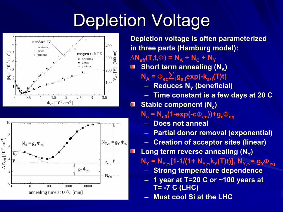
Fig.13: Annealing behaviour of the radiation induced change in the effective doping concentration ∆Neff at 60°C.
Figure 9: Dependence of Neff on the accumulated 1 MeV neutron equivalent fluence for standard and oxygen enriched FZ silicon irradiated with reactor neutrons (Ljubljana), 23 GeV protons (CERN PS) and 192 MeV pions (PSI).
Depletion voltage is often parameterized Depletion voltage is often parameterized in three parts (Hamburg model): in three parts (Hamburg model): ∆∆NNeffeff(T,t,(T,t,ΦΦ) = N) = NAA + N+ NCC + N+ NYY
Short term annealing (NShort term annealing (NAA))NNAA = = ΦΦeqeq iigga,ia,iexp(exp(--kkaa,,ii(T)t(T)t))–– Reduces NReduces NYY (beneficial)(beneficial)–– Time constant is a few days at 20 CTime constant is a few days at 20 C
Stable component (Stable component (NNcc))NNcc = N= Nc0c0(1(1--exp(exp(--ccΦΦeqeq))+g))+gccΦΦeqeq–– Does not anneal Does not anneal –– Partial donor removal (exponential)Partial donor removal (exponential)–– Creation of acceptor sites (linear)Creation of acceptor sites (linear)
Long term reverse annealing (NLong term reverse annealing (NYY))NNYY = N= NY,∞Y,∞[1[1--1/(1+ 1/(1+ NNY,∞Y,∞kkYY(T)t(T)t)], N)], NY,∞Y,∞= = ggYYΦΦeqeq–– Strong temperature dependenceStrong temperature dependence–– 1 year at T=20 C or ~100 years at 1 year at T=20 C or ~100 years at
T= T= --7 C (LHC)7 C (LHC)–– Must cool Must cool SiSi at the LHCat the LHC
0 0.5 1 1.5 2 2.5 3 3.5Φeq [1014cm-2]
1
2
3
4
5
6
7
|Nef
f| [1
012 c
m-3
]
100
200
300
400
Vde
p [V
] (3
00µm
)
neutronsneutrons
neutronsneutronspionspionsprotonsprotons
pionspionsprotonsprotons
oxygen rich FZ
standard FZstandard FZ
1 10 100 1000 10000annealing time at 60oC [min]
0
2
4
6
8
10
∆ N
eff [
1011
cm-3
]
NY,∞ = gY Φeq
NC
NC0
gC ΦeqgC Φeq
NA = ga ΦeqNA = ga Φeq
Σ
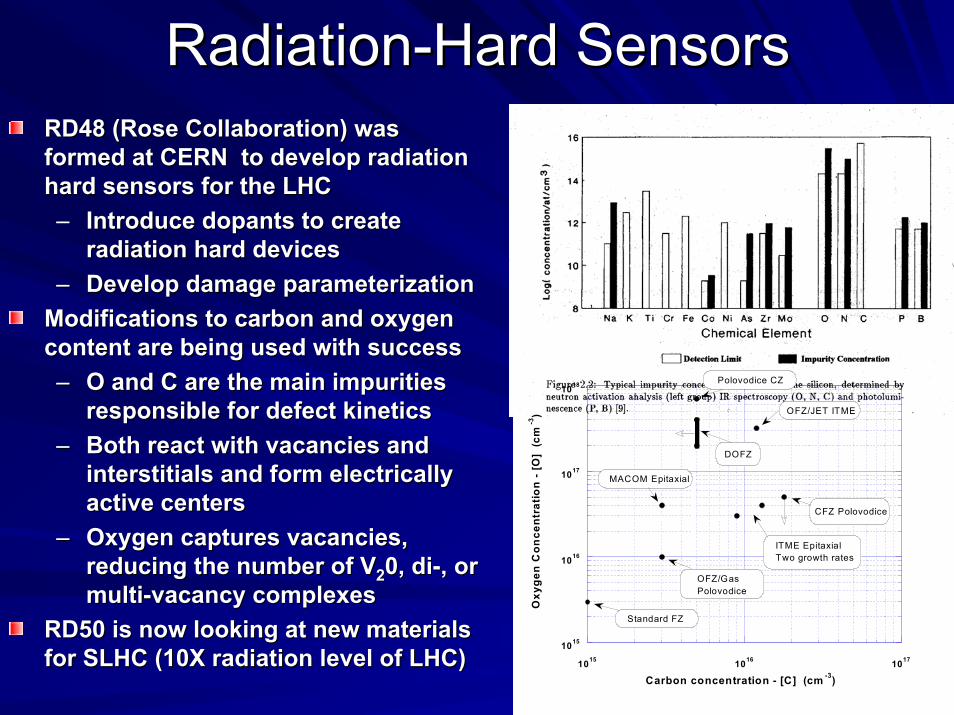
RadiationRadiation--Hard SensorsHard SensorsRD48 (Rose Collaboration) was RD48 (Rose Collaboration) was formed at CERN to develop radiation formed at CERN to develop radiation hard sensors for the LHC hard sensors for the LHC –– Introduce Introduce dopantsdopants to create to create
radiation hard devicesradiation hard devices–– Develop damage parameterizationDevelop damage parameterization
Modifications to carbon and oxygen Modifications to carbon and oxygen content are being used with successcontent are being used with success–– O and C are the main impurities O and C are the main impurities
responsible for defect kineticsresponsible for defect kinetics–– Both react with vacancies and Both react with vacancies and
interstitials and form electrically interstitials and form electrically active centersactive centers
–– Oxygen captures vacancies, Oxygen captures vacancies, reducing the number of Vreducing the number of V220, 0, didi--, or , or multimulti--vacancy complexesvacancy complexes
RD50 is now looking at new materials RD50 is now looking at new materials for SLHC (10X radiation level of LHC)
1015
1016
1017
1018
1015 1016 1017
Oxy
gen
Con
cent
ratio
n -
[O]
(cm
-3)
Carbon concentration - [C] (cm -3)
CFZ Polovodice
ITME EpitaxialTwo growth rates
MACOM Epitaxial
Polovodice CZ
DOFZ
Standard FZ
OFZ/JET ITME
OFZ/Gas Polovodice
for SLHC (10X radiation level of LHC)

Bulk Damage and OxygenationBulk Damage and Oxygenation
Fig.2: Oxygen-concentration profiles for standard and oxygen enriched FZ silicon wafers as measured by SIMS.
0 30 60 90 120 150depth [µm]
1016
5
1017
5
[O] [
atom
s/cm
3 ]
9d 1200oC 9d 1200oC 6h 1100oC 6h 1100oC
Oxygen and Carbon content is set during ingot growth and is also altered by diffusion– Standard high-purity float-zone
processing (FZ) plus high temperature processing (~1100 C for > day)
– Diffusion-oxygenation during float-zone (DOFZ) processing is also possible
Oxygen-enrichment of FZ Silicon:– Normal SiO2 field oxide grown
(~1000 C for 12 hours)– Additional heating to 1200 C in N2
(plot shows 6 hours vs 9 days)Why not use the industry-standard CZ silicon? – Low resistivity (100 Ωcm vs 2kΩcm)– High carbon content (1017 cm-3)Figure 10: Effective space charge density and full depletion voltage versus
proton fluence for standard, carbon-enriched and three types of oxygen diffused samples: 24, 48 and 72 hour diffusion at 1150°C [[i]].
βSt = 0.0154
β[O] = 0.0044 ÷0.0053
β[C] = 0.0437
0
1E+12
2E+12
3E+12
4E+12
5E+12
6E+12
7E+12
8E+12
9E+12
1E+13
0 1E+14 2E+14 3E+14 4E+14 5E+14
Proton fluence (24 GeV/c ) [cm-2]
|Nef
f| [c
m-3
]
0
100
200
300
400
500
VFD
for
300
µm th
ick
dete
ctor
[V]
Standard (P51)O-diffusion 24 hours (P52)O-diffusion 48 hours (P54)O-diffusion 72 hours (P56)Carbon-enriched (P503)

Oxygenation BenefitsOxygenation BenefitsOxygen enhancement is beneficial:Oxygen enhancement is beneficial:–– Effective Effective dopantdopant concentration (depletion voltage) can be concentration (depletion voltage) can be
improved by up to a factor of 3improved by up to a factor of 3–– Saturation of the concentration of reverse annealing clusters; Saturation of the concentration of reverse annealing clusters;
no longer proportional to no longer proportional to ΦΦ–– Longer time constant for reverse annealing Longer time constant for reverse annealing
Oxygenation only beneficial for charged radiation (larger numberOxygenation only beneficial for charged radiation (larger numberof vacancyof vacancy--interstitial pairs)interstitial pairs)
0 1 2 3 4 5 6 7Φeq [1014 cm-2]
0
0.2
0.4
0.6
0.8
1
1.2
NC [
1013
cm
-3]
oxygenated FZ
standard FZ
24 GeV/c proton irradiation
gc = 1.93 10-2 cm-1
gc = 5.61 10-3 cm-1
0 1 2 3 4 5 6 7Φeq [1014 cm-2]
0
0.5
1
1.5
2
2.5
NY [
1013
cm
-3]
oxygenated FZoxygenated FZ
24 GeV/c proton irradiation24 GeV/c proton irradiation
standard FZstandard FZ
Fig.18: Damage parameters NC for oxygenated and standard material as obtained
from annealing experiments at 60°C after irradiation with 24 GeV/c protons.
Fig.19: Damage parameters NY for oxygenated and standard material as obtained
from annealing experiments at 60°C after irradiation with 24 GeV/c protons.
Under study:– Neutron irradiation – Optimal parameters for
oxygenation– Why doesn’t oxygenated
Si follow the NIEL hypothesis (more impurities is bad)?

Pixel sensorsPixel sensors
l
A solution to get precise 3A solution to get precise 3--D information is to develop D information is to develop pixel sensors. pixel sensors. Hybrid pixelsHybrid pixels
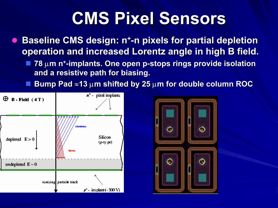
CMS Pixel SensorsCMS Pixel SensorsBaseline CMS design: nBaseline CMS design: n++--n pixels for partial depletion n pixels for partial depletion operation and increased operation and increased LorentzLorentz angle in high B field.angle in high B field.
78 78 µµm nm n++--implants. One open pimplants. One open p--stops rings provide isolation stops rings provide isolation and a resistive pathand a resistive path for biasing.for biasing.Bump Pad Bump Pad ≈≈13 13 µµm shifted by 25 m shifted by 25 µµm for double column ROCm for double column ROC

Requirements:Requirements:Breakdown voltage > 300V (we do Breakdown voltage > 300V (we do not see any breakdown in diodes up not see any breakdown in diodes up to 1000 V with 11 guard rings)to 1000 V with 11 guard rings)ReadRead--out side groundedout side groundedVoltage drop on guards on the Voltage drop on guards on the backsidebackside
Guard ring design
11 guard rings
6 guard rings
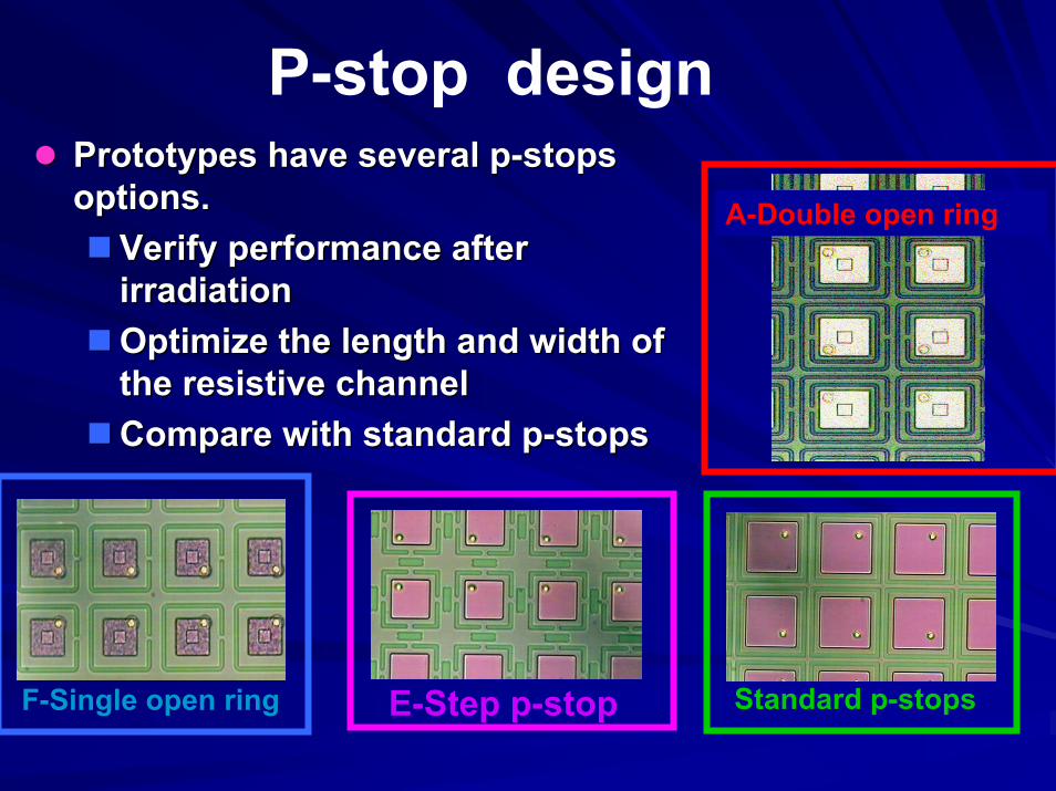
P-stop designPrototypes have several pPrototypes have several p--stops stops options.options.
Verify performance after Verify performance after irradiationirradiationOptimize the length and width of Optimize the length and width of the resistive channelthe resistive channelCompare with standard pCompare with standard p--stopsstops
Standard p-stopsF-Single open ring
A-Double open ring
E-Step p-stop

P-stop Performance
Dose 1e15 at -10 C
1.E-07
1.E-06
1.E-05
1.E-04
0 200 400 600 800 1000
Reverse Bias (V)
Leak
age
Cur
ent (
A)
W14P5-P+ W14P5-GRW4P2-P+ W4P2-GRW7P5-P+ W7P5-GRW14D43-P+ W14D43-GRGuard Ring Current
SENSOR Current
Excellent production quality: all Excellent production quality: all wafers have >80% good sensorswafers have >80% good sensorsAverage breakdown voltage Average breakdown voltage around 600 Varound 600 VNo breakdown after irradiation to No breakdown after irradiation to 1E151E15
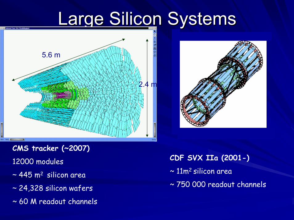
Large Silicon SystemsLarge Silicon Systems
5.6 m
2.4 m
CMS tracker (~2007)
12000 modules
~ 445 m2 silicon area
~ 24,328 silicon wafers
~ 60 M readout channels
CDF SVX IIa (2001-)
~ 11m2 silicon area
~ 750 000 readout channels
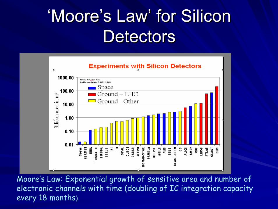
‘‘Moore’s Law’ for Silicon Moore’s Law’ for Silicon DetectorsDetectors
Moore’s Law: Exponential growth of sensitive area and number of electronic channels with time (doubling of IC integration capacity every 18 months)

Pioneering Silicon Strip Pioneering Silicon Strip DetectorsDetectors
fan out to readout electronics
E706 (FNAL 1987)NA11 (CERN 1981) sensor
o 24x36 mm2 active areao 8 layers of silicono 1m2 readout electronics!
o 50x50 mm2 active area
Silicon sensor and readout electronics technology closely coupled ⇒with electronics miniaturization (transistors, ICs, ASICs …) coming along,
silicon detectors quickly took off …

Contemporary Silicon Contemporary Silicon Detector ModulesDetector Modules
CDF SVX IIa half-ladder: two silicon sensors with readout electronics (SVX3b analog readout chip) mounted on first sensor
ATLAS SCT barrel module: four silicon sensors with center-tapped readout electronics (ABCD binary readout chip)

Large Silicon Detector Systems Large Silicon Detector Systems ……..
LEP Tevatron LHC
Whoops… P.Collins, ICHEP 2002
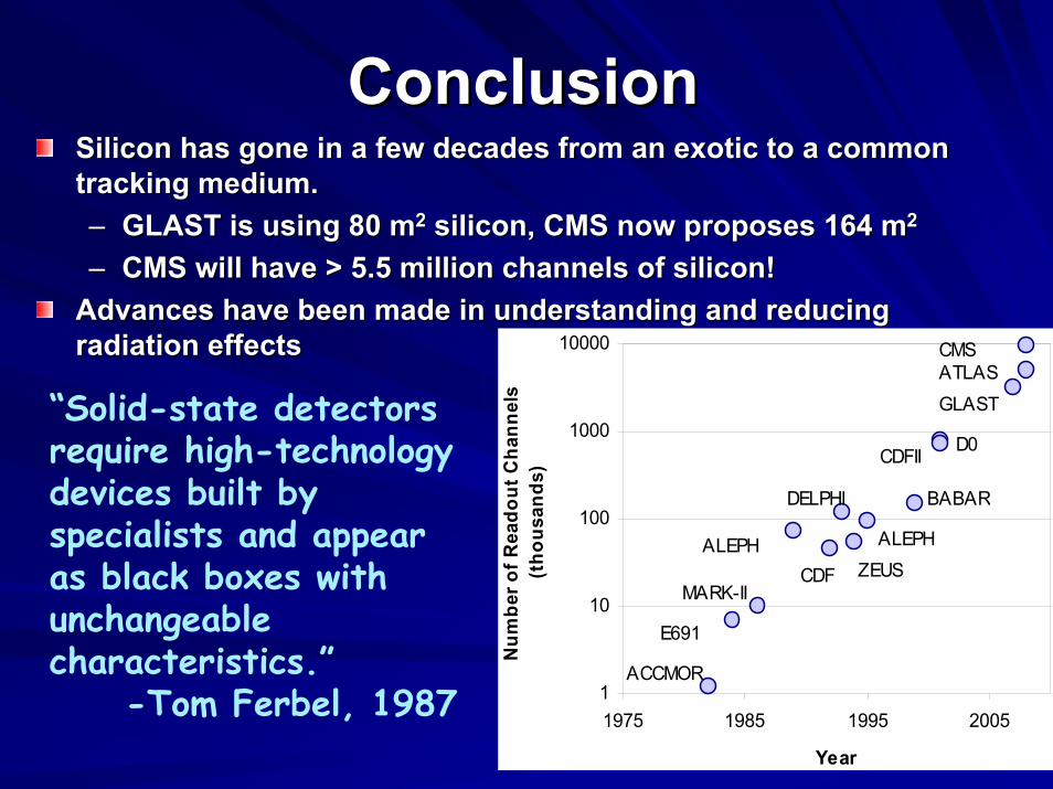
ConclusionConclusionSilicon has gone in a few decades from an exotic to a common Silicon has gone in a few decades from an exotic to a common tracking medium.tracking medium.–– GLAST is using 80 mGLAST is using 80 m22 silicon, CMS now proposes 164 msilicon, CMS now proposes 164 m22
–– CMS will have > 5.5 million channels of silicon!CMS will have > 5.5 million channels of silicon!Advances have been made in understanding and reducing Advances have been made in understanding and reducing radiation effectsradiation effects
1
10
100
1000
10000
1975 1985 1995 2005
Year
Num
ber o
f Rea
dout
Cha
nnel
s (t
hous
ands
)
CMSATLASGLAST
CDFII
BABAR
ALEPH
DELPHI
ZEUSCDFALEPH
MARK-II
ACCMOR
D0
E691
“Solid-state detectors require high-technology devices built by specialists and appear as black boxes with unchangeable characteristics.”
-Tom Ferbel, 1987

References References ……..SzeSze, Physics of semiconductor devices, Physics of semiconductor devicesHelmuthHelmuth SpeilerSpeiler lecture notes (wwwlecture notes (www--physics.kbl.gov/~spielerphysics.kbl.gov/~spieler))Rainer Rainer WallnyWallnyGino Gino BollaBolla UTEV seminar: UTEV seminar: http://http://www.fnal.gov/orgs/utev/past_speakers.htmlwww.fnal.gov/orgs/utev/past_speakers.htmlR. Lipton Academic lectures: R. Lipton Academic lectures: http://wwwhttp://www--ppd.fnal.gov/eppofficeppd.fnal.gov/eppoffice--w/Academic_Lectures/Past_Lectures.htmw/Academic_Lectures/Past_Lectures.htmSteve Worm notes on Radiation DamageSteve Worm notes on Radiation DamageSilicon Microstrip Detectors , A.Peisert, in " Instrumentation in High Energy Physics ", F.Sauli (ed), World Scientific, (1992). Animations from the Educational Java Applet (JAS) Service The applet resources are developed and maintained by Prof. C.R.Wie'sgroup at SUNY at Buffalo: : jas.eng.buffalo.edujas.eng.buffalo.edu
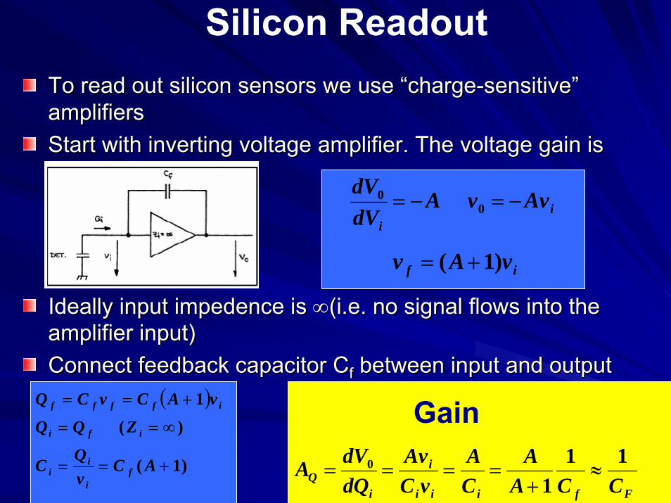
Silicon ReadoutTo read out silicon sensors we use “chargeTo read out silicon sensors we use “charge--sensitive” sensitive” amplifiersamplifiersStart with inverting voltage amplifier. The voltage gain is Start with inverting voltage amplifier. The voltage gain is
Ideally input Ideally input impedenceimpedence is is ∞∞(i.e. no signal flows into the (i.e. no signal flows into the amplifier input)amplifier input)Connect feedback capacitor Connect feedback capacitor CCff between input and outputbetween input and output
ii
AvvAdVdV
−=−= 00
if vAv )1( +=
( )
)1(
)(
1
+==
∞==
+==
ACvQC
ZQQ
vACvCQ
fi
ii
ifi
iffff
Ffiii
i
iQ CCA
ACA
vCAv
dQdVA 11
10 ≈
+====
Gain
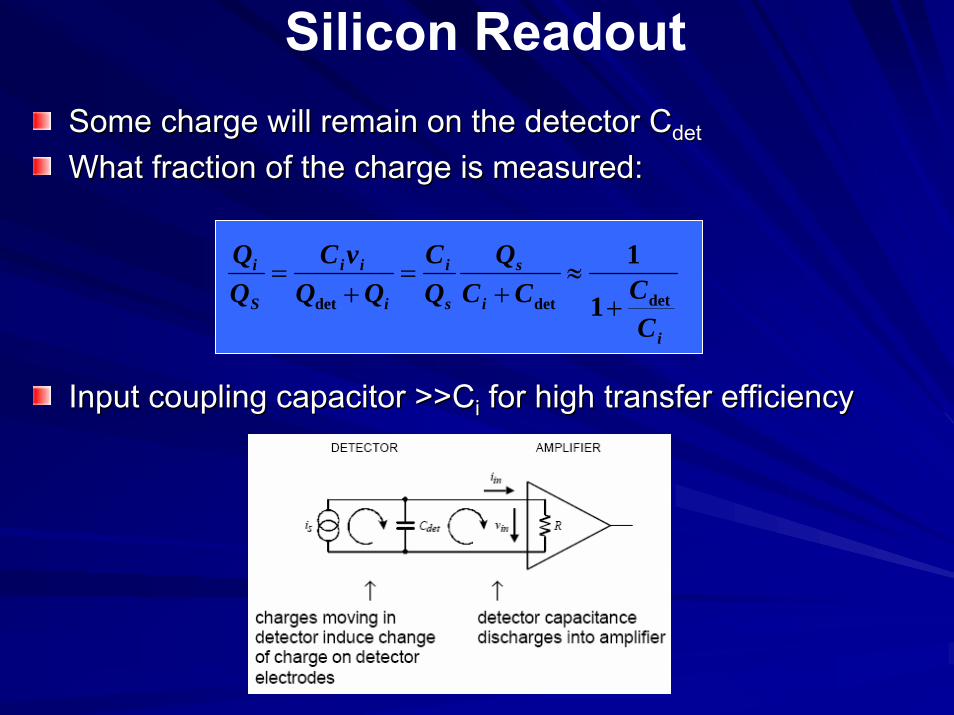
Silicon Readout Some charge will remain on the detector Some charge will remain on the detector CCdetdet
What fraction of the charge is measured:What fraction of the charge is measured:
Input coupling capacitor >>Input coupling capacitor >>CCii for high transfer efficiencyfor high transfer efficiency
i
i
s
s
i
i
ii
S
i
CCCC
QQC
QQvC
detdetdet 1
1
+≈
+=
+=

The Shockley Equation•• The The transconductancetransconductance curve iscurve is
IIDD = = IISS(e(eVVDD//ηηVVTT –– 1)1)•• IIDD is the current through the diode, Iis the current through the diode, ISS is the saturation current and Vis the saturation current and VDD is is
the applied biasing voltage.the applied biasing voltage.
•• VVTT is the thermal equivalent voltage and is approximately 26 mV atis the thermal equivalent voltage and is approximately 26 mV at room room temperature. The equation to find Vtemperature. The equation to find VTT at various temperatures is:at various temperatures is:
VVTT = = kTkTqq
k = 1.38 x 10k = 1.38 x 10--2323 J/K T = temperature in Kelvin q = 1.6 x 10J/K T = temperature in Kelvin q = 1.6 x 10--1919 CC
•• ηη is the emission coefficient for the diode. It is determined byis the emission coefficient for the diode. It is determined by the way the way the diode is constructed. It somewhat varies with diode currentthe diode is constructed. It somewhat varies with diode current. For a . For a silicon diode silicon diode ηη is around 2 for low currents and goes down to about 1 at is around 2 for low currents and goes down to about 1 at higher currentshigher currents