an integrated four-port dc-dc converter-cei0080
TRANSCRIPT
1
AN INTEGRATED FOUR-PORT DC/DC CONVERTER
FOR RENEWABLE ENERGY APPLICATIONS

2
ABSTRACT
This paper proposes a novel converter topology that interfaces four power
ports: two sources, one bidirectional storage port, and one isolated load port. The
proposed four-port dc/dc converter is derived by simply adding two switches and
two diodes to the traditional half-bridge topology. Zero-voltage switching is
realized for all four main switches. Three of the four ports can be tightly regulated
by adjusting their independent duty-cycle values, while the fourth port is left
unregulated to maintain the power balance for the system. Circuit analysis and
design considerations are presented; the dynamic modeling and close-loop design
guidance are given as well. Experimental results verify the proposed topology and
confirm its ability to achieve tight independent control over three power-
processing paths. This topology promises significant savings in component count
and losses for renewable energy power-harvesting systems.
3
INTRODUCTION
Present industry is increasingly shifting towards automation. Two principle
components of today’s industrial automations are programmable controllers and
robots. In order to aid the tedious work and to serve the mankind, today there is a
general tendency to develop an intelligent operation.
The proposed system “AN INTEGRATED FOUR-PORT DC/DC
CONVERTERFOR RENEWABLE ENERGY APPLICATIONS” is designed
and developed to accomplish the various tasks in an adverse environment of an
industry. The intelligent This project is an owe to the technical advancement. This
prototype system can be applied effectively and efficiently in an expanded
dimension to fit for the requirement of industrial, research and commercial
applications.
Microcontroller is the heart of the device which handles all the sub devices
connected across it. We have used as microcontroller. It has flash type
reprogrammable memory. It has some peripheral devices to play this project
perform. It also provides sufficient power to inbuilt peripheral devices. We need
not give individually to all devices. The peripheral devices also activates as low
power operation mode. These are the advantages are appear here.

4
BLOCK DIAGRAM:

5
BLOCK DIAGRAM DESCRIPTION:
PIC MICRO CONTROLLER
CONCEPTS OF MICROCONTROLLER :
Microcontroller is a general
purpose device, which integrates a number of the components of a
microprocessor system on to single chip. It has inbuilt CPU, memory and
peripherals to make it as a mini computer. A microcontroller combines on to the
same microchip:
The CPU core
Memory(both ROM and RAM)
Some parallel digital i/o
Microcontrollers will combine other devices such as:
A timer module to allow the microcontroller to perform tasks for certain
time periods.
A serial i/o port to allow data to flow between the controller and other
devices such as a PIC or another microcontroller.
An ADC to allow the microcontroller to accept analogue input data for
processing.

6
Microcontrollers are :
Smaller in size
Consumes less power
Inexpensive
Micro controller is a stand alone unit ,which can perform functions
on its own without any requirement for additional hardware like i/o ports and
external memory.
The heart of the microcontroller is the CPU core. In the past, this has traditionally
been based on a 8-bit microprocessor unit. For example Motorola uses a basic
6800 microprocessor core in their 6805/6808 microcontroller devices.
In the recent years, microcontrollers have been
developed around specifically designed CPU cores, for example the microchip PIC
range of microcontrollers.
INTRODUCTION TO PIC :
The microcontroller that has been used for this
project is from PIC series. PIC microcontroller is the first RISC based
microcontroller fabricated in CMOS (complimentary metal oxide semiconductor)
that uses separate bus for instruction and data allowing simultaneous access of
program and data memory.
The main advantage of CMOS and RISC
combination is low power consumption resulting in a very small chip size with a

7
small pin count. The main advantage of CMOS is that it has immunity to noise
than other fabrication techniques.
PIC (16F877) :
Various microcontrollers offer different kinds of
memories. EEPROM, EPROM, FLASH etc. are some of the memories of which
FLASH is the most recently developed. Technology that is used in pic16F877 is
flash technology, so that data is retained even when the power is switched off.
Easy Programming and Erasing are other features of PIC 16F877.
PIC START PLUS PROGRAMMER :
The PIC start plus development system from
microchip technology provides the product development engineer with a highly
flexible low cost microcontroller design tool set for all microchip PIC micro
devices. The picstart plus development system includes PIC start plus development
programmer and mplab ide.
The PIC start plus programmer gives the product developer
ability to program user software in to any of the supported microcontrollers. The
PIC start plus software running under mplab provides for full interactive control
over the programmer.
SPECIAL FEATURES OF PIC MICROCONTROLLER :
CORE FEATURES :

8
• High-performance RISC CPU
• Only 35 single word instructions to learn
• All single cycle instructions except for program branches which are two cycle
• Operating speed: DC - 20 MHz clock input
DC - 200 ns instruction cycle
• Up to 8K x 14 words of Flash Program Memory,
Up to 368 x 8 bytes of Data Memory (RAM)
Up to 256 x 8 bytes of EEPROM data memory
• Pin out compatible to the PIC16C73/74/76/77
• Interrupt capability (up to 14 internal/external
• Eight level deep hardware stack
• Direct, indirect, and relative addressing modes
• Power-on Reset (POR)
• Power-up Timer (PWRT) and Oscillator Start-up Timer (OST)
• Watchdog Timer (WDT) with its own on-chip RC Oscillator for reliable
operation
• Programmable code-protection
• Power saving SLEEP mode
• Selectable oscillator options

9
• Low-power, high-speed CMOS EPROM/EEPROM technology
• Fully static design
• In-Circuit Serial Programming (ICSP) via two pins
• Only single 5V source needed for programming capability
• In-Circuit Debugging via two pins
• Processor read/write access to program memory
• Wide operating voltage range: 2.5V to 5.5V
• High Sink/Source Current: 25 mA
• Commercial and Industrial temperature ranges
• Low-power consumption:
< 2mA typical @ 5V, 4 MHz
20mA typical @ 3V, 32 kHz
< 1mA typical standby current
PERIPHERAL FEATURES :
• Timer0: 8-bit timer/counter with 8-bit prescaler
• Timer1: 16-bit timer/counter with prescaler, can be incremented during sleep
via external crystal/clock
• Timer2: 8-bit timer/counter with 8-bit period register, prescaler and postscaler

10
• Two Capture, Compare, PWM modules
Capture is 16-bit, max resolution is 12.5 ns,
Compare is 16-bit, max resolution is 200 ns,
PWM max. resolution is 10-bit
• 10-bit multi-channel Analog-to-Digital converter
• Synchronous Serial Port (SSP) with SPI. (Master Mode) and I2C.
(Master/Slave)
• Universal Synchronous Asynchronous Receiver Transmitter (USART/SCI) with
9- bit address detection.
• Brown-out detection circuitry for Brown-out Reset (BOR)
ARCHITECTURE OF PIC 16F877 :
The complete architecture of PIC
16F877 is shown in the fig 2.1. Table 2.1 gives details about the specifications of
PIC 16F877. Fig 2.2 shows the complete pin diagram of the IC PIC 16F877.
ARCHITECTURE OF PIC 16F877

11
SPECIFICATIONS
PIN DIAGRAM OF PIC 16F877
DEVICE PROGRAM FLASH DATA
MEMORY
DATA
EEPROM
PIC
16F877 8K 368 Bytes 256 Bytes

12
PIN OUT DESCRIPTION

13
Legend: I = input O = output I/O = input/output P = power
— = Not used TTL = TTL input ST = Schmitt Trigger input
Note
1. This buffer is a Schmitt Trigger input when configured as an external interrupt
2. This buffer is a Schmitt Trigger input when used in serial programming mode.

14
3. This buffer is a Schmitt Trigger input when configured as general purpose I/O
and a TTL
input when used in the Parallel Slave Port mode (for interfacing to a
microprocessor bus).
4. This buffer is a Schmitt Trigger input when configured in RC oscillator mode
and a
CMOS input otherwise.

15
Legend: I = input O = output I/O = input/output P = power
— = Not used TTL = TTL input ST = Schmitt Trigger input
Note :
1. This buffer is a Schmitt Trigger input when configured as an external interrupt.
2. This buffer is a Schmitt Trigger input when used in serial programming mode.

16
3. This buffer is a Schmitt Trigger input when configured as general purpose I/O
and a TTL
input when used in the Parallel Slave Port mode (for interfacing to a
microprocessor bus).
4. This buffer is a Schmitt Trigger input when configured in RC oscillator mode
and a
CMOS input otherwise.
2.5 I/O PORTS :
Some pins for these I/O ports are multiplexed with an alternate
function for the peripheral features on the device. In general, when a peripheral is
enabled, that pin may not be used as a general purpose I/O pin.
Additional Information on I/O ports may be found in the IC
micro™ Mid-Range Reference Manual,
PORTA AND THE TRISA REGISTER :
PORTA is a 6-bit wide bi-directional port. The corresponding
data direction register is TRISA. Setting a TRISA bit (=1) will make the
corresponding PORTA pin an input, i.e., put the corresponding output driver in a
Hi-impedance mode. Clearing a TRISA bit (=0) will make the corresponding
PORTA pin an output, i.e., put the contents of the output latch on the selected pin.
Reading the PORTA register reads the status of the

17
pins whereas writing to it will write to the port latch. All write operations are read-
modify-write operations. Therefore a write to a port implies that the port pins are
read; this value is modified, and then written to the port data latch. Pin RA4 is
multiplexed with the Timer0 module clock input to become the RA4/T0CKI pin.
The RA4/T0CKI pin is a Schmitt Trigger input and an open drain output. All other
RA port pins have TTL input levels and full CMOS output drivers. Other PORTA
pins are multiplexed with analog inputs and analog VREF input. The operation of
each pin is selected by clearing/setting the control bits in the ADCON1 register
(A/D Control Register1).
The TRISA register controls the direction of the RA pins, even when they
are being used as analog inputs. The user must ensure the bits in the TRISA
register are maintained set when using them as analog inputs.
PORT A FUNCTION
Legend: TTL = TTL input, ST = Schmitt Trigger input

18
SUMMARY OF REGISTERS ASSOCIATED WITH PORTA
Legend: x = unknown, u = unchanged, - = unimplemented locations
read as '0'. Shaded cells are not used by PORTA.
PORTB AND TRISB REGISTER :
PORTB is an 8-bit wide bi-directional port.
The corresponding data direction register is TRISB. Setting a TRISB bit (=1) will
make the corresponding PORTB pin an input, i.e., put the corresponding output
driver in a hi-impedance mode. Clearing a TRISB bit (=0) will make the
corresponding PORTB pin an output, i.e., put the contents of the output latch on
the selected pin. Three pins of PORTB are multiplexed with the Low Voltage
Programming function; RB3/PGM, RB6/PGC and RB7/PGD. The alternate
functions of these pins are described in the Special Features Section. Each of the
PORTB pins has a weak internal pull-up. A single control bit can turn on all the
pull-ups.

19
This is performed by clearing bit RBPU
(OPTION_REG<7>). The weak pull-up is automatically turned off when the port
pin is configured as an output. The pull-ups are disabled on a Power-on Reset.
Four of PORT B’s pins, RB7:RB4, have an interrupt on
change feature. Only pins configured as inputs can cause this interrupt to occur
(i.e. any RB7:RB4 pin configured as an output is excluded from the interrupt on
change comparison). The input pins (of RB7:RB4) are compared with the old value
latched on the last read of PORTB. The “mismatch” outputs of RB7:RB4 are
OR’ed together to generate the RB Port Change Interrupt with flag bit RBIF
(INTCON<0>). This interrupt can wake the device from SLEEP. The user, in the
interrupt service routine, can clear the interrupt in the following manner:
a) Any read or write of PORTB. This will end the mismatch condition.
b) Clear flag bit RBIF. A mismatch condition will continue to set flag
bit RBIF. Reading PORTB will end the mismatch condition, and allow flag bit
RBIF to be cleared. The interrupt on change feature is recommended for wake-up
on key depression operation and operations where PORTB is only used for the
interrupt on change feature. Polling of PORTB is not recommended while using
the interrupt on change feature. This interrupt on mismatch feature, together with
software configurable pull-ups on these four pins, allow easy interface to a keypad
and make it possible for wake-up on key depression
20
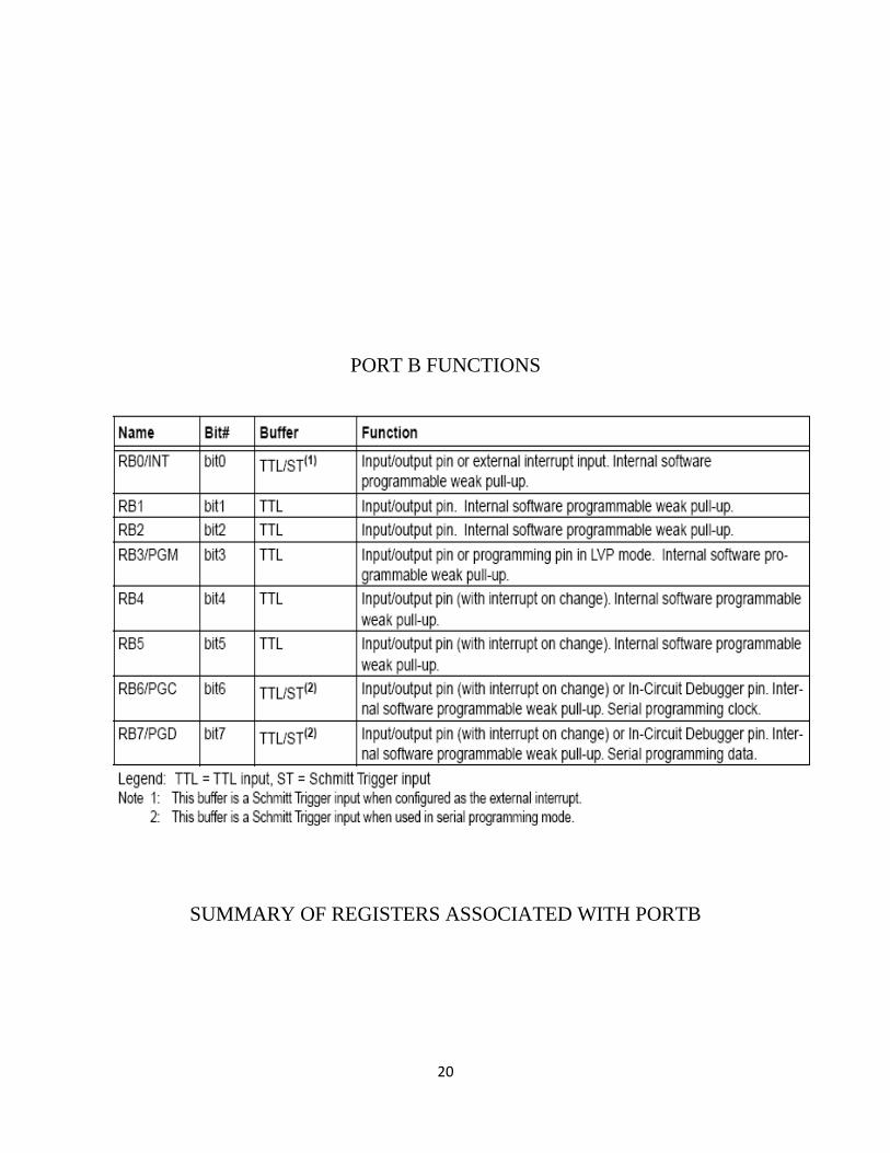
PORT B FUNCTIONS
SUMMARY OF REGISTERS ASSOCIATED WITH PORTB

21
PORTC AND THE TRISC REGISTER :
PORTC is an 8-bit wide bi-directional port.
The corresponding data direction register is TRISC. Setting a TRISC bit (=1) will
make the corresponding PORTC pin an input, i.e., put the corresponding output
driver in a hi-impedance mode. Clearing a TRISC bit (=0) will make the
corresponding PORTC pin an output, i.e., put the contents of the output latch on
the selected pin. PORTC is multiplexed with several peripheral functions. PORTC
pins have Schmitt Trigger input buffers.
When the I2C module is enabled, the
PORTC (3:4) pins can be configured with normal I2C levels or with SMBUS
levels by using the CKE bit (SSPSTAT <6>). When enabling peripheral functions,
care should be taken in defining TRIS bits for each PORTC pin. Some peripherals
override the TRIS bit to make a pin an output, while other peripherals override the
TRIS bit to make a pin an input. Since the TRIS bit override is in effect while the
peripheral is enabled, read-modify write instructions (BSF, BCF, XORWF) with
TRISC as destination should be avoided. The user should refer to the
corresponding peripheral section for the correct TRIS bit settings.

22
PORTC FUNCTIONS
SUMMARY OF REGISTERS ASSOCIATED WITH PORTC
PORTD AND TRISD REGISTERS :
This section is not applicable to the 28-pin
devices. PORTD is an 8-bit port with Schmitt Trigger input buffers. Each pin is

23
individually configurable as an input or output. PORTD can be configured as an 8-
bit wide microprocessor Port (parallel slave port) by setting control bit PSPMODE
(TRISE<4>). In this mode, the input buffers are TTL.
PORTD FUNCTIONS
SUMMARY OF REGISTERS ASSOCIATED WITH PORTD
PORTE AND TRISE REGISTER :

24
PORTE has three pins RE0/RD/AN5,
RE1/WR/AN6 and RE2/CS/AN7, which are individually configurable as inputs or
outputs. These pins have Schmitt Trigger input buffers.
The PORTE pins become control inputs for the
microprocessor port when bit PSPMODE (TRISE<4>) is set. In this mode, the user
must make sure that the TRISE<2:0> bits are set (pins are configured as digital
inputs). Ensure ADCON1 is configured for digital I/O. In this mode the input
buffers are TTL.
PORTE pins are multiplexed with analog inputs.
When selected as an analog input, these pins will read as '0's. TRISE controls the
direction of the RE pins, even when they are being used as analog inputs. The user
must make sure to keep the pins configured as inputs when using them as analog
inputs.
PORTE FUNCTIONS

25
SUMMARY OF REGISTERS ASSOCIATED WITH PORTE
\ MEMORY ORGANISATION :
There are three memory blocks in each of
the PIC16F877 MUC’s. The program memory and Data Memory have separate
buses so that concurrent access can occur.

26
PROGRAM MEMORY ORGANISATION :
The PIC16f877 devices have a 13-bit
program counter capable of addressing 8K *14 words of FLASH program
memory. Accessing a location above the physically implemented address will
cause a wraparound.
The RESET vector is at 0000h and the interrupt vector is at 0004h.
DATA MEMORY ORGANISTION :
The data memory is partitioned into multiple
banks which contain the General Purpose Registers and the special functions
Registers. Bits RP1 (STATUS<6) and RP0 (STATUS<5>) are the bank selected
bits.
RP1:RP0 Banks
00 0
01 1
10 2
11 3
Each bank extends up to 7Fh (1238 bytes).
The lower locations of each bank are reserved for the Special Function Registers.
Above the Special Function Registers are General Purpose Registers, implemented
as static RAM. All implemented banks contain special function registers. Some
frequently used special function registers from one bank may be mirrored in
another bank for code reduction and quicker access.

27
PIC16F877 REGISTER FILE MAP

28
GENERAL PURPOSE REGISTER FILE :
The register file can be accessed either
directly or indirectly through the File Selected Register (FSR). There are some
Special Function Registers used by the CPU and peripheral modules for controlling
the desired operation of the device. These registers are implemented as static
RAM. The Special Function Registers can be classified into two sets; core (CPU)
and peripheral. Those registers associated with the core functions.
INSTRUCTION SET SUMMARY :
Each PIC 16f877 instruction is a 14-bit
word, divided into an OPCODE which specifies the instruction type and one or
more operand which further specify the operation of the instruction. The
PIC16F877 instruction set summary in Table 2.13 lists byte-oriented, bit-
oriented, and literal and control operations. It shows the opcode Field
descriptions.
OPCODE FIELD DESCRIPTIONS

29
For byte-oriented instructions, ‘f’
represents a file register designator and ’d’ represents a destination designator. The
file register designator specifies which file register is to be used by the instruction.
The destination designator specified where the result of the operation is to be
placed. If ‘d’ is zero, the result is placed in the w register. If ‘d’ is one, the result is
placed in the file register specified in the instruction.
For bit-oriented instructions, ‘b’ represents
a bit field designator which selects the number of the bit affected by the operation,
which ‘f’ represents the address of the file in which the bits is located. For literal
and control operations, ‘k’ represents an eight or eleven bit constant or literal
value.

30
The instruction set is highly orthogonal and is grouped into three basic
categories:
• Byte-oriented operations
• Bit-oriented operations
• Literal and control operations
All instructions are executed within one
single instruction cycle, unless a conditional test is true or the program counter is
changed as a result of an instruction. In this case, the execution takes two
instruction cycles with the second cycle executed as a NOP. One instruction cycle
consists of four oscillator periods. Thus, for an oscillator frequency of 4 MHz, the
normal instruction execution time is 1 ms. If a conditional test is true or the
program counter is changed as a result of an instruction, then the instruction
execution time is 2 ms.

31
16F877 INSTRUCTION SET

32
GENERAL FORMAT FOR INSTRUCTIONS :
SOLAR PANEL:

33
A solar panel (photovoltaic module or photovoltaic panel) is a packaged
interconnected assembly of solar cells, also known as photovoltaic cells. The solar
panel is used as a component in a larger photovoltaic system to offer electricity for
commercial and residential applications.
Because a single solar panel can only produce a limited amount of power, many
installations contain several panels. This is known as a photovoltaic array. A
photovoltaic installation typically includes an array of solar panels, an inverter,
batteries and interconnection wiring.
Solar panels use light energy (photons) from the sun to generate electricity through
the photovoltaic effect. The structural (load carrying) member of a module can
either be the top layer (superstrate) or the back layer (substrate). The majority of
modules use wafer-based crystalline silicon cells or a thin-film cell based on
cadmium telluride or silicon. Crystalline silicon, which is commonly used in the
wafer form in photovoltaic (PV) modules, is derived from silicon, a commonly
used semi-conductor.
In order to use the cells in practical applications, they must be:
connected electrically to one another and to the rest of the system
protected from mechanical damage during manufacture, transport, installation and
use (in particular against hail impact, wind and snow loads). This is especially
important for wafer-based silicon cells which are brittle.
protected from moisture, which corrodes metal contacts and interconnects, (and
for thin-film cells the transparent conductive oxide layer) thus decreasing
performance and lifetime.

34
Most modules are usually rigid, but there are some flexible modules available,
based on thin-film cells.
Electrical connections are made in series to achieve a desired output voltage and/or
in parallel to provide a desired amount of current source capability.
Diodes are included to avoid overheating of cells in case of partial shading. Since
cell heating reduces the operating efficiency it is desirable to minimize the heating.
Very few modules incorporate any design features to decrease temperature,
however installers try to provide good ventilation behind the module.[1]
New designs of module include concentrator modules in which the light is
concentrated by an array of lenses or mirrors onto an array of small cells. This
allows the use of cells with a very high-cost per unit area (such as gallium
arsenide) in a cost-competitive way.
Depending on construction, the photovoltaic can cover a range of frequencies of
light and can produce electricity from them, but sometimes cannot cover the entire
solar spectrum (specifically, ultraviolet, infrared and low or diffused light). Hence
much of incident sunlight energy is wasted when used for solar panels, although
they can give far higher efficiencies if illuminated with monochromatic light.
Another design concept is to split the light into different wavelength ranges and
direct the beams onto different cells tuned to the appropriate wavelength ranges.[2]
This is projected to raise efficiency by 50%. Also, the use of infrared photovoltaic
cells can increase the efficiencies, producing power at night.
BATTERY:

35
An electrical battery is one or more electrochemical cells that convert stored
chemical energy into electrical energy.[1] Since the invention of the first battery (or
"voltaic pile") in 1800 by Alessandro Volta, batteries have become a common
power source for many household and industrial applications. According to a 2005
estimate, the worldwide battery industry generates US$48 billion in sales each
year,[2] with 6% annual growth.[3]
There are two types of batteries: primary batteries (disposable batteries), which are
designed to be used once and discarded when they are exhausted, and secondary
batteries (rechargeable batteries), which are designed to be recharged and used
multiple times. Miniature cells are used to power devices such as hearing aids and
wristwatches; larger batteries provide standby power for telephone exchanges or
computer data centers.
History

36
The symbol for a battery in a circuit diagram. It originated as a schematic drawing
of the earliest type of battery, a voltaic pile.
Strictly, a battery is a collection of multiple electrochemical cells, but in popular
usage battery often refers to a single cell.[1] The first electrochemical cell was
developed by the Italian physicist Alessandro Volta in 1792, and in 1800 he
invented the first battery—for him, a "pile" of cells.[4]
The usage of "battery" to describe electrical devices dates to Benjamin Franklin,
who in 1748 described multiple Leyden jars (early electrical capacitors) by analogy
to a battery of cannons.[5] Thus Franklin's usage to describe multiple Leyden jars
predated Volta's use of multiple galvanic cells.[6]. It is speculated, but not
established, that several ancient artifacts consisting of copper sheets and iron bars,
and known as Baghdad batteries may have been galvanic cells.[7]
Volta's work was stimulated by the Italian anatomist and physiologist Luigi
Galvani, who in 1780 noticed that dissected frog's legs would twitch when struck
by a spark from a Leyden jar, an external source of electricity.[8] In 1786 he noticed
that twitching would occur during lightning storms.[9] After many years Galvani
learned how to produce twitching without using any external source of electricity.
In 1791 he published a report on "animal electricity."[10] He created an electric
circuit consisting of the frog's leg (FL) and two different metals A and B, each

37
metal touching the frog's leg and each other, thus producing the circuit A-FL-B-A-
FL-B...etc. In modern terms, the frog's leg served as both the electrolyte and the
sensor, and the metals served as electrodes. He noticed that even though the frog
was dead, its legs would twitch when he touched them with the metals.
Within a year, Volta realized the frog's moist tissues could be replaced by
cardboard soaked in salt water, and the frog's muscular response could be replaced
by another form of electrical detection. He already had studied the electrostatic
phenomenon of capacitance, which required measurements of electric charge and
of electrical potential ("tension"). Building on this experience, Volta was able to
detect electric current through his system, also called a Galvanic cell. The terminal
voltage of a cell that is not discharging is called its electromotive force (emf), and
has the same unit as electrical potential, named (voltage) and measured in volts, in
honor of Volta. In 1800, Volta invented the battery by placing many voltaic cells in
series, literally piling them one above the other. This voltaic pile gave a greatly
enhanced net emf for the combination,[11] with a voltage of about 50 volts for a 32-
cell pile.[12] In many parts of Europe batteries continue to be called piles.[13][14]
Volta did not appreciate that the voltage was due to chemical reactions. He thought
that his cells were an inexhaustible source of energy,[15] and that the associated
chemical effects (e.g. corrosion) were a mere nuisance, rather than an unavoidable
consequence of their operation, as Michael Faraday showed in 1834.[16] According
to Faraday, cations (positively charged ions) are attracted to the cathode,[17] and
anions (negatively charged ions) are attracted to the anode.[18]
Although early batteries were of great value for experimental purposes, in practice
their voltages fluctuated and they could not provide a large current for a sustained
period. Later, starting with the Daniell cell in 1836, batteries provided more

38
reliable currents and were adopted by industry for use in stationary devices,
particularly in telegraph networks where they were the only practical source of
electricity, since electrical distribution networks did not exist at the time.[19] These
wet cells used liquid electrolytes, which were prone to leakage and spillage if not
handled correctly. Many used glass jars to hold their components, which made
them fragile. These characteristics made wet cells unsuitable for portable
appliances. Near the end of the nineteenth century, the invention of dry cell
batteries, which replaced the liquid electrolyte with a paste, made portable
electrical devices practical.[20]
Since then, batteries have gained popularity as they became portable and useful for
a variety of purposes.[21]
How batteries work

39
A voltaic cell for demonstration purposes. In this example the two half-cells are
linked by a salt bridge separator that permits the transfer of ions, but not water
molecules.
A battery is a device that converts chemical energy directly to electrical energy.[22]
It consists of a number of voltaic cells; each voltaic cell consists of two half cells
connected in series by a conductive electrolyte containing anions and cations. One
half-cell includes electrolyte and the electrode to which anions (negatively charged
ions) migrate, i.e., the anode or negative electrode; the other half-cell includes
electrolyte and the electrode to which cations (positively charged ions) migrate,
i.e., the cathode or positive electrode. In the redox reaction that powers the battery,
reduction (addition of electrons) occurs to cations at the cathode, while oxidation
(removal of electrons) occurs to anions at the anode.[23] The electrodes do not touch
each other but are electrically connected by the electrolyte. Many cells use two
half-cells with different electrolytes. In that case each half-cell is enclosed in a
container, and a separator that is porous to ions, but not the bulk of the electrolytes,
prevents mixing.
Each half cell has an electromotive force (or emf), determined by its ability to
drive electric current from the interior to the exterior of the cell. The net emf of the
40
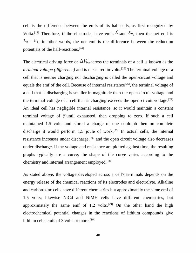
cell is the difference between the emfs of its half-cells, as first recognized by
Volta.[12] Therefore, if the electrodes have emfs and , then the net emf is
; in other words, the net emf is the difference between the reduction
potentials of the half-reactions.[24]
The electrical driving force or across the terminals of a cell is known as the
terminal voltage (difference) and is measured in volts.[25] The terminal voltage of a
cell that is neither charging nor discharging is called the open-circuit voltage and
equals the emf of the cell. Because of internal resistance[26], the terminal voltage of
a cell that is discharging is smaller in magnitude than the open-circuit voltage and
the terminal voltage of a cell that is charging exceeds the open-circuit voltage.[27]
An ideal cell has negligible internal resistance, so it would maintain a constant
terminal voltage of until exhausted, then dropping to zero. If such a cell
maintained 1.5 volts and stored a charge of one coulomb then on complete
discharge it would perform 1.5 joule of work.[25] In actual cells, the internal
resistance increases under discharge,[26] and the open circuit voltage also decreases
under discharge. If the voltage and resistance are plotted against time, the resulting
graphs typically are a curve; the shape of the curve varies according to the
chemistry and internal arrangement employed.[28]
As stated above, the voltage developed across a cell's terminals depends on the
energy release of the chemical reactions of its electrodes and electrolyte. Alkaline
and carbon-zinc cells have different chemistries but approximately the same emf of
1.5 volts; likewise NiCd and NiMH cells have different chemistries, but
approximately the same emf of 1.2 volts.[29] On the other hand the high
electrochemical potential changes in the reactions of lithium compounds give
lithium cells emfs of 3 volts or more.[30]

41
Categories and types of batteries


43
From top to bottom: SR41/AG3, SR44/AG13 (button cells), a 9-volt PP3 battery,
an AAA cell, an AA cell, a C cell, a D Cell, and a large 3R12. The ruler's unit is in
centimeters.
Batteries are classified into two broad categories, each type with advantages and
disadvantages.[31]
Primary batteries irreversibly (within limits of practicality) transform
chemical energy to electrical energy. When the initial supply of reactants is
exhausted, energy cannot be readily restored to the battery by electrical
means.[32]
Secondary batteries can be recharged; that is, they can have their chemical
reactions reversed by supplying electrical energy to the cell, restoring their
original composition.[33]
Historically, some types of primary batteries used, for example, for telegraph
circuits, were restored to operation by replacing the components of the battery
consumed by the chemical reaction.[34] Secondary batteries are not indefinitely
rechargeable due to dissipation of the active materials, loss of electrolyte and
internal corrosion.
Primary batteries
Primary batteries can produce current immediately on assembly. Disposable
batteries are intended to be used once and discarded. These are most commonly
used in portable devices that have low current drain, are only used intermittently,
or are used well away from an alternative power source, such as in alarm and
communication circuits where other electric power is only intermittently available.
Disposable primary cells cannot be reliably recharged, since the chemical reactions

44
are not easily reversible and active materials may not return to their original forms.
Battery manufacturers recommend against attempting to recharge primary cells.[35]
Common types of disposable batteries include zinc-carbon batteries and alkaline
batteries. Generally, these have higher energy densities than rechargeable
batteries,[36] but disposable batteries do not fare well under high-drain applications
with loads under 75 ohms (75 Ω).[31]
Secondary batteries
Secondary batteries must be charged before use; they are usually assembled with
active materials in the discharged state. Rechargeable batteries or secondary cells
can be recharged by applying electric current, which reverses the chemical
reactions that occur during its use. Devices to supply the appropriate current are
called chargers or rechargers.
The oldest form of rechargeable battery is the lead-acid battery.[37] This battery is
notable in that it contains a liquid in an unsealed container, requiring that the
battery be kept upright and the area be well ventilated to ensure safe dispersal of
the hydrogen gas produced by these batteries during overcharging. The lead-acid
battery is also very heavy for the amount of electrical energy it can supply. Despite
this, its low manufacturing cost and its high surge current levels make its use
common where a large capacity (over approximately 10Ah) is required or where
the weight and ease of handling are not concerns.

45
A common form of the lead-acid battery is the modern car battery, which can
generally deliver a peak current of 450 amperes.[38] An improved type of liquid
electrolyte battery is the sealed valve regulated lead acid (VRLA) battery, popular
in the automotive industry as a replacement for the lead-acid wet cell. The VRLA
battery uses an immobilized sulfuric acid electrolyte, reducing the chance of
leakage and extending shelf life.[39] VRLA batteries have the electrolyte
immobilized, usually by one of two means:
Gel batteries (or "gel cell") contain a semi-solid electrolyte to prevent
spillage.
Absorbed Glass Mat (AGM) batteries absorb the electrolyte in a special
fiberglass matting.
Other portable rechargeable batteries include several "dry cell" types, which are
sealed units and are therefore useful in appliances such as mobile phones and
laptop computers. Cells of this type (in order of increasing power density and cost)
include nickel-cadmium (NiCd), nickel-zinc (NiZn), nickel metal hydride (NiMH)
and lithium-ion (Li-ion) cells.[40] By far, Li-ion has the highest share of the dry cell
rechargeable market.[3] Meanwhile, NiMH has replaced NiCd in most applications
due to its higher capacity, but NiCd remains in use in power tools, two-way radios,
and medical equipment.[3] NiZn is a new technology that is not yet well established
commercially.
Recent developments include batteries with embedded functionality such as
USBCELL, with a built-in charger and USB connector within the AA format,

46
enabling the battery to be charged by plugging into a USB port without a
charger,[41] and low self-discharge (LSD) mix chemistries such as Hybrio,[42]
ReCyko,[43] and Eneloop,[44] where cells are precharged prior to shipping.
WIND MILL:
A windmill is a machine which converts the energy of wind into rotational motion
by means of adjustable vanes called sails. The main use is for a grinding mill
powered by the wind, reducing a solid or coarse substance into pulp or minute
grains, by crushing, grinding, or pressing.[1][2] Windmills have also provided
energy to sawmills, paper mills, hammermills, and windpumps for obtaining fresh
water from underground or for drainage (especially of land below sea level).

47
Vertical-axis windmills
The first practical windmills were the vertical axle windmills invented in eastern
Persia (what is now Afghanistan), as recorded by the Persian geographer Estakhri
in the 9th century.[6][7] The authenticity of an earlier anecdote of a windmill
involving the second caliph Umar (AD 634–644) is questioned on the grounds that
it appears in a 10th-century document.[8] Made of six to twelve sails covered in

48
reed matting or cloth material, these windmills were used to grind grain or draw up
water, and were quite different from the later European horizontal-axis versions.
Windmills were in widespread use across the Middle East and Central Asia, and
later spread to China and India from there.[9]
Some popular treatments of the subject have speculated that, by the 9th century,
the Persian-style vertical-axle mills spread to Europe through Al-Andalus (Islamic
Spain).[10] This has been denied by the specialist of medieval European technology,
Lynn White Jr., who points out that there is no evidence (archaeological or
documentary) that the Afghanistan-style vertical-axle windmill spread as far west
as Al-Andalus,[11] and notes that "all Iberian windmills rotated on horizontal axles
until towards the middle of the fifteenth century."[12] Another historian of
technology, Michael Jonathan Taunton Lewis, suggested an alternative route of
transmission for the Islamic horizontal-shaft windmill, with its diffusion to the
Byzantine Empire and its subsequent transformation into the vertical-shaft
windmill in Europe.[13] Late medieval vertical-axle windmills similar to the
Islamic/Persian design can be found along this route, particularly in Karpathos,
Greece, and Kandia, Crete. The Crusades has also been suggested as another
possible route of transmission, though in the sense of "stimulus diffusion," where
the idea was diffused rather than the technology itself.[14] However, the debate
about whether the European vertical-shaft windmill evolved from the Islamic
horizontal-shaft windmill or was an independent development remains
unresolved.[13]

49
Horizontal-axis windmills
Horizontal-axle windmills that turn to face the wind
In northwestern Europe, the horizontal-axle or vertical windmill (so called due to
the dimension of the movement of its sails) dates from the last quarter of the 12th
century in the triangle of northern France, eastern England and Flanders. Lynn
White Jr. claims that the first certain reference to the European horizontal-axle
windmill is dated to 1185 in Weedley, Yorkshire.[16] (This predates Joseph
Needham's claim that the earliest known reference is from the 1191 chronicle of
Jocelin of Brakelond, in which a Dean Herbert of East Anglia supposedly
competed with the mills of the abbey of Bury St Edmunds).[17] These earliest mills
were used to grind cereals. The evidence at present is that the earliest type was the
sunk post mill, so named because of the large upright post on which the mill's main
structure (the "body" or "buck") is balanced. By mounting the body this way, the

50
mill is able to rotate to face the wind direction; an essential requirement for
windmills to operate economically in North-Western Europe, where wind
directions are variable. By the end of the thirteenth century the masonry tower mill,
on which only the timber cap rotated rather than the whole body of the mill, had
been introduced. In the Netherlands these stone towerlike mills are called "round or
eight-sided stone stage mills, ground-sailers (windmills with sails reaching almost
down to the ground), mound mills, etc." (Dutch: ronde/achtkante stenen stelling
molens, grond-zeilers, beltmolens, etc.). Dutch tower mills ("torenmolens") are
always cylindrical (such as atop castle or city wall towers). Because only the cap of
the tower mill needed to be turned the main structure could be made much taller,
allowing the sails to be made longer, which enabled them to provide useful work
even in low winds. Such mills often have a small auxiliary set of sails called a
fantail at the rear of the cap and at right angles to the sails; this rotates the cap
through gearing so that the sails face into the wind.

51
Multi-sailed windmills
The majority of windmills had four sails. An increase in the number of sails meant
that an increase in power could be obtained, at the expense of an increase in the
weight of the sail assembly. The earliest record of a multi-sailed mill in the United
Kingdom was the five sail Flint Mill, Leeds, mentioned in a report by John
Smeaton in 1774. Multi-sailed windmills were said to run smoother than four sail
windmills. In Lincolnshire, more multi-sailed windmills were found than anywhere
else in the United Kingdom. There were five, six and eight sail windmills.[26]
If a four sail windmill suffers a damaged sail, the one opposite can be removed and
the mill will work with two sails, generating about 60% of the power that it would
with all four sails. A six sail mill can run with two, three, four or six sails. An eight
sail mill can run with two, four, six or eight sails, thus allowing a number of
options if an accident occurs. A five sail mill can only run with all five sails. If one
is damaged then the mill is stopped until it is replaced.
MOSFET DRIVER CIRCUIT:
52
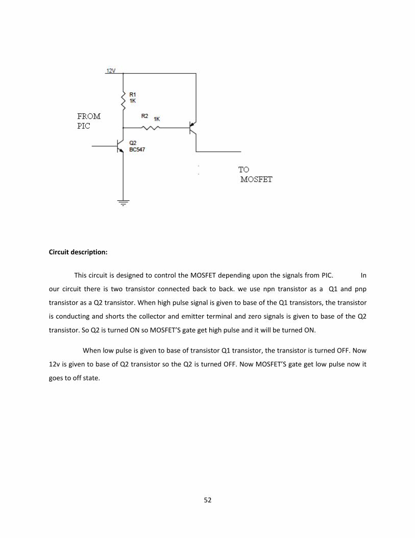
Circuit description:
This circuit is designed to control the MOSFET depending upon the signals from PIC. In
our circuit there is two transistor connected back to back. we use npn transistor as a Q1 and pnp
transistor as a Q2 transistor. When high pulse signal is given to base of the Q1 transistors, the transistor
is conducting and shorts the collector and emitter terminal and zero signals is given to base of the Q2
transistor. So Q2 is turned ON so MOSFET’S gate get high pulse and it will be turned ON.
When low pulse is given to base of transistor Q1 transistor, the transistor is turned OFF. Now
12v is given to base of Q2 transistor so the Q2 is turned OFF. Now MOSFET’S gate get low pulse now it
goes to off state.

53
Voltage Signal from Transistor Q1 Transistor Q2 MOSFET
PIC Microcontroller
1 on on on
0 off off off
MOSFET
MOSFET operation
For the operation of MOS devices discussed next, an authoritative reference is
Tsividis [2].
Metal–oxide–semiconductor structure
Metal–oxide–semiconductor structure on P-type silicon
A traditional metal–oxide–semiconductor (MOS) structure is obtained by
depositing a layer of silicon dioxide (SiO2) and a layer of metal (polycrystalline
silicon is commonly used instead of metal) on top of a semiconductor die. As the

54
silicon dioxide is a dielectric material its structure is equivalent to a planar
capacitor, with one of the electrodes replaced by a semiconductor.
When a voltage is applied across a MOS structure, it modifies the distribution of
charges in the semiconductor. If we consider a P-type semiconductor (with NA the
density of acceptors, p the density of holes; p = NA in neutral bulk), a positive
voltage, VGB, from gate to body (see figure) creates a depletion layer by forcing the
positively charged holes away from the gate-insulator/semiconductor interface,
leaving exposed a carrier-free region of immobile, negatively charged acceptor
ions. See doping (semiconductor). If VGB is high enough, a high concentration of
negative charge carriers forms in an inversion layer located in a thin layer next to
the interface between the semiconductor and the insulator. (Unlike the MOSFET,
discussed below, where the inversion layer electrons are supplied rapidly from the
source/drain electrodes, in the MOS capacitor they are produced much more
slowly by thermal generation through carrier generation and recombination centers
in the depletion region.) Conventionally, the gate voltage at which the volume
density of electrons in the inversion layer is the same as the volume density of
holes in the body is called the threshold voltage.
This structure with P-type body is the basis of the N-type MOSFET, which
requires the addition of an N-type source and drain regions.

55
1.1.1 MOSFET structure and channel formation
Cross section of an NMOS without channel formed: OFF state
Cross section of an NMOS with channel formed: ON state
A metal–oxide–semiconductor field-effect transistor (MOSFET) is based on the
modulation of charge concentration by a MOS capacitance between a body
electrode and a gate electrode located above the body and insulated from all other
device regions by an oxide. The MOSFET includes two additional terminals
(source and drain), each connected to individual highly doped regions that are
separated by the body region. These regions can be either p or n type, but they
must both be of the same type, and of opposite type to the body region. The highly

56
doped source and drain regions typically are denoted by a '+' following the type of
doping. The body is not highly doped, as denoted by the lack of a '+' sign.
If the MOSFET is an n-channel or nMOS FET, then the source and drain are 'n+'
regions and the body is a 'p' region. As described above, with sufficient gate
voltage, above a threshold voltage value, electrons from the source (and possibly
also the drain) enter the inversion layer or n-channel at the interface between the p
region and the oxide. This conducting channel extends between the source and the
drain, and current is conducted through it when a voltage is applied between source
and drain.
For gate voltages below the threshold value, the channel is lightly populated, and
only a very small subthreshold leakage current can flow between the source and
the drain.
If the MOSFET is a p-channel or pMOS FET, then the source and drain are 'p+'
regions and the body is a 'n' region. When a negative gate-source voltage (positive
source-gate) is applied, it creates a p-channel at the surface of the n region,
analogous to the n-channel case, but with opposite polarities of charges and
voltages. When a voltage less negative than the threshold value (a negative voltage
for p-Channel) is applied between gate and source, the channel disappears and only
a very small subthreshold current can flow between the source and the drain.
The source is so named because it is the source of the charge carriers (electrons for
n-channel, holes for p-channel) that flow through the channel; similarly, the drain
is where the charge carriers leave the channel.

57
1.1.2 Modes of operation
The operation of a MOSFET can be separated into three different modes,
depending on the voltages at the terminals. In the following discussion, a
simplified algebraic model is used that is accurate only for old technology. Modern
MOSFET characteristics require computer models that have rather more complex
behavior. For example, see Liu [3] and the device modeling list in [1].
For an enhancement-mode, n-channel MOSFET the three operational modes are:
Cut-off or Sub-threshold or Weak Inversion Mode
When V GS < Vth:
where Vth is the threshold voltage of the device.
According to the basic threshold model, the transistor is turned off, and there is
no conduction between drain and source. In reality, the Boltzmann distribution of
electron energies allows some of the more energetic electrons at the source to
enter the channel and flow to the drain, resulting in a subthreshold current that is
an exponential function of gate–source voltage. While the current between drain
and source should ideally be zero when the transistor is being used as a turned-
off switch, there is a weak-inversion current, sometimes called subthreshold
leakage.
In weak inversion the current varies exponentially with gate-to-source bias VGS as
given approximately by:[4][5]
,
where ID0 = current at VGS = Vth and the slope factor n is given by

58
n = 1 + CD / COX,
with CD = capacitance of the depletion layer and COX = capacitance of the oxide
layer. In a long-channel device, there is no drain voltage dependence of the
current once VDS > > VT, but as channel length is reduced drain-induced barrier
lowering introduces drain voltage dependence that depends in a complex way
upon the device geometry (for example, the channel doping, the junction doping
and so on). Frequently threshold voltage Vth for this mode is defined as the gate
voltage at which a selected value of current ID0 occurs, for example, ID0 = 1 μA,
which may not be the same Vth-value used in the equations for the following
modes.
ISOLATION TRANSFORMER
An isolation transformer is a transformer used to transfer electrical power from a
source of alternating current (AC) power to some equipment or device while
isolating the powered device from the power source, usually for safety. Isolation
transformers provide galvanic isolation and are used to protect against electric
shock, to suppress electrical noise in sensitive devices, or to transfer power
between two circuits which must not be connected together.
Suitably designed isolation transformers block interference caused by ground
loops. Isolation transformers with electrostatic shields are used for power supplies
for sensitive equipment such as computers or laboratory instruments.

59
Strictly speaking any true transformer, whether used to transfer signals or power, is
isolating, as the primary and secondary are not connected by conductors but only
by induction.
However, only transformers whose primary purpose is to isolate circuits (opposed
to the more common transformer function of voltage conversion), are routinely
described as isolation transformers.
Given this function, a transformer sold for isolation is often built with special
insulation between primary and secondary, and is tested, specified, and marked to
withstand a high voltage between windings, typically in the 1000 to 4000 volt
range.
Sometimes the term is exceptionally used to clarify that some transformer,
although not primarily intended for isolation, is a true transformer rather than an
autotransformer (whose primary and secondary are not isolated from each other).[1]
Even step-down power transformers required, amongst other things, to protect low-
voltage equipment from mains voltage by isolating the secondary and primary such
as are used in older "wall warts", are not usually described specifically as
"isolation transformers".
Some very small transformers—e.g. 4 transformers in one tiny dual in-line (DIL)
chip package—used to isolate high-frequency low-voltage (logic) pulse circuits
(e.g., 500V RMS primary–secondary for one second), are described as isolation
transformers[1][2]
Isolation transformers are commonly designed with careful attention to capacitive
coupling between the two windings. The capacitance between primary and
secondary windings would also couple AC current from the primary to the

60
secondary. A grounded Faraday shield between the primary and the secondary
greatly reduces the coupling of common-mode noise. This may be another winding
or a metal strip surrounding a winding.
Differential noise can magnetically couple from the primary to the secondary of an
isolation transformer, and must be filtered out if a problem.
Sometimes a balanced secondary with an earthed center is used. This can reduce
earth leakage in equipment used in wet locations. The maximum voltage above
earth is halved, reducing the risk of shock if anything live is touched.
Applications
In electronics testing and servicing isolation transformer is a 1:1 (under load)
power transformer used for safety. Without it, exposed live metal in a device under
test is at a hazardous voltage relative to grounded objects such as a heating radiator
or oscilloscope ground lead (a particular hazard with some old vacuum-tube
equipment with live chassis). With the transformer, as there is no conductive
connection between transformer secondary and earth, there is no danger in
touching a live part of the circuit while another part of the body is earthed.
Electrical isolation is considered to be particularly important on medical
equipment, and special standards apply. Often the system must additionally be
designed so that fault conditions do not interrupt power, but generate a warning.[3]
Isolation transformers are also used for the power supply of devices not at ground
potential. An example is the Austin transformer for the power supply of air-traffic
obstacle warning lamps on radio antenna masts. Without the isolation transformer,

61
the lighting circuits on the mast would conduct radio-frequency energy to ground
through the power supply.
Metal boats are subject to corrosion if they use earthed power from shore when
moored, due to galvanic currents that flow through the water between shore earth
and the hull. This can be avoided by using an isolation transformer with the
primary and case connected to shore earth, and the secondary "floating".[4] A metal
safety screen between primary and secondary is connected to shore earth; in the
event of a fault current in the primary (due, e.g., to insulation breakdown) it will
cause the fault current to return and trip a shore-based circuit breaker rather than
making the hull live.

62
OVERALL CIRCUIT DIAGRAM:
POWER SUPPLY:
Block diagram
The ac voltage, typically 220V rms, is connected to a transformer, which
steps that ac voltage down to the level of the desired dc output. A diode rectifier
then provides a full-wave rectified voltage that is initially filtered by a simple
capacitor filter to produce a dc voltage. This resulting dc voltage usually has some
ripple or ac voltage variation.
A regulator circuit removes the ripples and also remains the same dc value
even if the input dc voltage varies, or the load connected to the output dc voltage
changes. This voltage regulation is usually obtained using one of the popular
voltage regulator IC units.
Block diagram (Power supply)
Working principle

63
Transformer
The potential transformer will step down the power supply voltage (0-
230V) to (0-6V) level. Then the secondary of the potential transformer will be
connected to the precision rectifier, which is constructed with the help of op–
amp. The advantages of using precision rectifier are it will give peak voltage
output as DC, rest of the circuits will give only RMS output.
Bridge rectifier
When four diodes are connected as shown in figure, the circuit is called as
bridge rectifier. The input to the circuit is applied to the diagonally opposite
corners of the network, and the output is taken from the remaining two corners.
Let us assume that the transformer is working properly and there is a
positive potential, at point A and a negative potential at point B. the positive
potential at point A will forward bias D3 and reverse bias D4.
The negative potential at point B will forward bias D1 and reverse D2. At
this time D3 and D1 are forward biased and will allow current flow to pass
through them; D4 and D2 are reverse biased and will block current flow.
The path for current flow is from point B through D1, up through RL,
through D3, through the secondary of the transformer back to point B. this path is
indicated by the solid arrows. Waveforms (1) and (2) can be observed across D1
and D3.

64
One-half cycle later the polarity across the secondary of the transformer
reverse, forward biasing D2 and D4 and reverse biasing D1 and D3. Current flow
will now be from point A through D4, up through RL, through D2, through the
secondary of T1, and back to point A. This path is indicated by the broken arrows.
Waveforms (3) and (4) can be observed across D2 and D4. The current flow
through RL is always in the same direction. In flowing through RL this current
develops a voltage corresponding to that shown waveform (5). Since current
flows through the load (RL) during both half cycles of the applied voltage, this
bridge rectifier is a full-wave rectifier.
One advantage of a bridge rectifier over a conventional full-wave rectifier is
that with a given transformer the bridge rectifier produces a voltage output that is
nearly twice that of the conventional full-wave circuit.
This may be shown by assigning values to some of the components shown in
views A and B. assume that the same transformer is used in both circuits. The peak
voltage developed between points X and y is 1000 volts in both circuits. In the
conventional full-wave circuit shown—in view A, the peak voltage from the center
tap to either X or Y is 500 volts. Since only one diode can conduct at any instant,
the maximum voltage that can be rectified at any instant is 500 volts.
The maximum voltage that appears across the load resistor is nearly-but
never exceeds-500 v0lts, as result of the small voltage drop across the diode. In the
bridge rectifier shown in view B, the maximum voltage that can be rectified is the
full secondary voltage, which is 1000 volts. Therefore, the peak output voltage
across the load resistor is nearly 1000 volts. With both circuits using the same
transformer, the bridge rectifier circuit produces a higher output voltage than the
conventional full-wave rectifier circuit.

65
IC voltage regulators
Voltage regulators comprise a class of widely used ICs. Regulator IC
units contain the circuitry for reference source, comparator amplifier, control
device, and overload protection all in a single IC. IC units provide regulation of
either a fixed positive voltage, a fixed negative voltage, or an adjustably set
voltage. The regulators can be selected for operation with load currents from
hundreds of milli amperes to tens of amperes, corresponding to power ratings
from milli watts to tens of watts.

66
Circuit diagram (Power supply)
A fixed three-terminal voltage regulator has an unregulated dc input
voltage, Vi, applied to one input terminal, a regulated dc output voltage, Vo, from
a second terminal, with the third terminal connected to ground.
The series 78 regulators provide fixed positive regulated voltages from 5 to
24 volts. Similarly, the series 79 regulators provide fixed negative regulated
voltages from 5 to 24 volts.
For ICs, microcontroller, LCD --------- 5 volts
For alarm circuit, op-amp, relay circuits ---------- 12 volts

67
LCD DISPLAY WITH PIC
We connect the lcd display with PIC through PORT D.

68
PORTD AND TRISD REGISTER :
PORTD is an 8-bit wide bi-directional port.
The corresponding data direction register is TRISD. Setting a TRISD bit (=1) will
make the corresponding PORTD pin an input, i.e., put the corresponding output
driver in a hi-impedance mode. Clearing a TRISD bit (=0) will make the
corresponding PORTD pin an output.
PORTD AND TRISD REGISTERS:
This section is not applicable to the 28-pin
devices. PORTD is an 8-bit port with Schmitt Trigger input buffers. Each pin is
individually configurable as an input or output. PORTD can be configured as an 8-
bit wide microprocessor Port (parallel slave port) by setting control bit PSPMODE
(TRISE<4>). In this mode, the input buffers are TTL.
PORTD FUNCTIONS
SUMMARY OF REGISTERS ASSOCIATED WITH PORTD

69
a) Any read or write of PORTD. This will end the mismatch
condition.
b) Clear flag bit RBIF. A mismatch condition will continue to
set flag bit RBIF. Reading PORTD will end the mismatch condition, and
allow flag bit RBIF to be cleared. The interrupt on change feature is
recommended for wake-up on key depression operation and operations
where PORTD is only used for the interrupt on change feature. Polling of
PORTD is not recommended while using the interrupt on change feature.
This interrupt on mismatch feature, together with software configurable pull-
ups on these four pins, allow easy interface to a keypad and make it possible
for wake-up on key depression

70

71
PCB DESIGN
Design and Fabrication of Printed circuit boards
INTRODUCTION:
Printed circuit boards, or PCBs, form the core of electronic equipment
domestic and industrial. Some of the areas where PCBs are intensively used are
computers, process control, telecommunications and instrumentation.
MANUFATCURING:
The manufacturing process consists of two methods; print and etch, and
print, plate and etch. The single sided PCBs are usually made using the print and
etch method. The double sided plate through – hole (PTH) boards are made by the
print plate and etch method.
The production of multi layer boards uses both the methods. The inner layers
are printed and etch while the outer layers are produced by print, plate and etch
after pressing the inner layers.
SOFTWARE:

72
The software used in our project to obtain the schematic layout is
MICROSIM.
PANELISATION:
Here the schematic transformed in to the working positive/negative films. The
circuit is repeated conveniently to accommodate economically as many circuits
as possible in a panel, which can be operated in every sequence of subsequent
steps in the PCB process. This is called penalization. For the PTH boards, the
next operation is drilling.
DRILLING:
PCB drilling is a state of the art operation. Very small holes are drilled with
high speed CNC drilling machines, giving a wall finish with less or no smear or
epoxy, required for void free through hole plating.
PLATING:
The heart of the PCB manufacturing process. The holes drilled in the board
are treated both mechanically and chemically before depositing the copper by the
electro less copper platting process.

73
ETCHING:
Once a multiplayer board is drilled and electro less copper deposited, the
image available in the form of a film is transferred on to the out side by photo
printing using a dry film printing process. The boards are then electrolytic plated
on to the circuit pattern with copper and tin. The tin-plated deposit serves an etch
resist when copper in the unwanted area is removed by the conveyor’s spray
etching machines with chemical etch ants. The etching machines are attached to an
automatic dosing equipment, which analyses and controls etch ants concentrations
SOLDERMASK:
Since a PCB design may call for very close spacing between conductors, a
solder mask has to be applied on the both sides of the circuitry to avoid the
bridging of conductors. The solder mask ink is applied by screening. The ink is
dried, exposed to UV, developed in a mild alkaline solution and finally cured by
both UV and thermal energy.
HOT AIR LEVELLING:

74
After applying the solder mask, the circuit pads are soldered using the hot air
leveling process. The bare bodies fluxed and dipped in to a molten solder bath.
While removing the board from the solder bath, hot air is blown on both sides of
the board through air knives in the machines, leaving the board soldered and
leveled. This is one of the common finishes given to the boards. Thus the double
sided plated through whole printed circuit board is manufactured and is now ready
for the components to be soldered.

75
MPLAB
MPLAB IDE is an integrated development environment that provides
development engineers with the flexibility to develop and debug firmware for
various Microchip devices
MPLAB IDE is a Windows-based Integrated Development Environment for the
Microchip Technology Incorporated PICmicrocontroller (MCU) and dsPIC digital
signal controller (DSC) families. In the MPLAB IDE, you can:
Create source code using the built-in editor.
Assemble, compile and link source code using various language tools. An
assembler, linker and librarian come with MPLAB IDE. C compilers are
available from Microchip and other third party vendors.
Debug the executable logic by watching program flow with a simulator,
such as MPLAB SIM, or in real time with an emulator, such as MPLAB
ICE. Third party emulators that work with MPLAB IDE are also available.
Make timing measurements.
View variables in Watch windows.
Program firmware into devices with programmers such as PICSTART Plus
or PRO MATE II.
Find quick answers to questions from the MPLAB IDE on-line Help.

76
MPLAB SIMULATOR
MPLAB SIM is a discrete-event simulator for the PIC microcontroller (MCU)
families. It is integrated into MPLAB IDE integrated development environment.
The MPLAB SIM debugging tool is designed to model operation of Microchip
Technology's PIC microcontrollers to assist users in debugging software for these
devices
IC PROG
The PRO MATE II is a Microchip microcontroller device programmer. Through
interchangeable programming socket modules, PRO MATE II enables you to
quickly and easily program the entire line of Microchip PICmicro microcontroller
devices and many of the Microchip memory parts.
PRO MATE II may be used with MPLAB IDE running under supported Windows
OS's (see Read me for PRO MATE II.txt for support list), with the command-line
controller PROCMD or as a stand-alone programmer
COMPILER-HIGH TECH C
A program written in the high level language called C; which will be converted
into PICmicro MCU machine code by a compiler. Machine code is suitable for use
by a PICmicro MCU or Microchip development system product like MPLAB IDE.

77
PIC START PLUS PROGRAMMER:
The PIC start plus development system from microchip technology
provides the product development engineer with a highly flexible low cost
microcontroller design tool set for all microchip PIC micro devices. The pic start
plus development system includes PIC start plus development programmer and
MPLAB IDE.
The PIC start plus programmer gives the product developer ability to
program user software in to any of the supported microcontrollers. The PIC start
plus software running under MPLAB provides for full interactive control over the
programmer.
ADVANTAGES
LOW COST
RELIABILITY
EASY TO IMPLEMENTATION
APPLICATION

78
CONCLUSION
The progress in science & technology is a non-stop process. New things and new technology
are being invented. As the technology grows day by day, we can imagine about the future in
which thing we may occupy every place.
The proposed system based on Atmel microcontroller is found to be more
compact, user friendly and less complex, which can readily be used in order to
perform. Several tedious and repetitive tasks. Though it is designed keeping in
mind about the need for industry, it can extended for other purposes such as
commercial & research applications. Due to the probability of high technology
(Atmel microcontroller) used this” AN INTEGRATED FOUR-PORT DC/DC
CONVERTERFOR RENEWABLE ENERGY APPLICATIONS” is fully
software controlled with less hardware circuit. The feature makes this system is the
base for future systems.
The principle of the development of science is that “nothing is impossible”. So we
shall look forward to a bright & sophisticated world
REFERENCE
MILL MAN J and HAWKIES C.C. “INTEGRATED
ELECTRONICS” MCGRAW HILL, 1972

79
ROY CHOUDHURY D, SHAIL JAIN, “ LINEAR INTEGRATED
CIRCUIT”, New Age International Publishers, New Delhi,2000
“THE 8051 MICROCONTROLLER AND EMBEDDED SYSTEM”
by Mohammad Ali Mazidi.
WEBSITES:
http://www.atmel.com/
http://www.microchip.com/
www.8052.com
http://www.beyondlogic.org

80
http://www.ctv.es/pckits/home.html
http://www.aimglobal.org/

81