an extremely low noise heterojunction impatt
TRANSCRIPT

IEEE TRANSACTIONS ON ELECTRON DEVICES, VOL. 44, NO. 12, DECEMBER 1997 2143
An Extremely Low Noise Heterojunction IMPATTJ. K. Mishra, A. K. Panda, and G. N. Dash
Abstract—The avalanche noise characteristics of InP/GaInAs(Ga0:47In0:53As) and InP/GaInAsP (Ga0:33In0:67As0:7P0:3) dou-ble drift region (DDR) heterostructure IMPact Avalanche TransitTime (IMPATT’s) have been studied. The heterostructure IM-PATT’s in general are found to be less noisy compared to theirhomostructure counterparts and in particular the InP/GaInAsDDR is found to generate extremely low noise when the ternarylayer width is properly selected. A noise measure of 7.7 dB hasbeen observed at 190 GHz for a GaInAs layer width of 140 nm.Further, a study on the noise contribution from the individualspace steps of the depletion layer due to individual noise sourcesin the generation region has revealed some interesting differ-ences between those of homostructure and heterostructure diodes.Finally, a criterion for low-noise design is also suggested.
I. INTRODUCTION
T HE InP/GaInAs and InP/GaInAsP lattice matched ma-terial systems have been attractive for heterojunction
IMPact Avalanche Transit Time (IMPATT’s) since the fab-rication of these systems for devices like laser diode andAvalanche Photo Diode (APD) is now a common practice.High efficiency and improved performance from these het-erojunction IMPATT’s have already been reported [1], [2].The high-frequency limitations caused by tunneling currenthas also been discussed [3], [4]. However, a detailed analysisof avalanche noise for heterojunction IMPATT, which is animportant consideration for IMPATT device study is not seenin published literature.1 Recently we have developed a general-ized computer simulation method to study the avalanche noisein MIxed Tunneling and Avalanche Transit Time (MITATT)devices [8]. In this paper, we present a detailed study onthe noise characteristics of InP, InP/GaInAs and InP/GaInAsPDDR diodes using our above simulation method. The resultsof our simulation indicate that the InP/GaInAs material combi-nation with a proper choice of the width for the GaInAs layermay find application as an extremely low noise heterojunctionIMPATT.
Manuscript received July 29, 1996; revised May 26, 1997. The review ofthis paper was arranged by Editor M. Fukuma.
J. K. Mishra is with G. M. (Autonomous) College, Sambalpur, Orissa768004, India.
A. K. Panda was with the Department of Physics, Sambalpur University,Sambalpur, Orissa 768019, India. He is now with National Institute of Scienceand Technology, Berhampur University, Berhampur, Orissa 760007, India.
G. N. Dash is with the Department of Physics, Sambalpur University,Sambalpur, Orissa 768019, India.
Publisher Item Identifier S 0018-9383(97)08286-5.1The GaAs/AlGaAs material combination has also drawn attention for
heterostructure IMPATT with a different concept, namely, Double VelocityAvalanche Transit Time mode (DOVATT) [5]–[7]. But we feel that the formerconcept [1]–[4] would permit greater flexibilty in the design of IMPATT fornoise control.
II. SIMULATION METHOD
A one-dimensional model of MITATT diode is consideredfor the noise analysis. The basic device structure is shown inFig. 1. The ternary/quaternary material has been chosen forthe high field zone due to their higher generation rates (bothavalanche and tunneling), whereas InP with low generationrate is selected for the low field zone. The carrier generationis almost confined to the ternary/quaternary layer, whichconstitute the generation region. Noise is generated in thegeneration region due to the statistical nature of the impactionization process. We, therefore, assume tunneling to be aquiet process and the avalanche process to be composed ofa noiseless generation rate and a noise generation rate.Let be the rate at which the carriers are generated at
(position of noise source) in the generation region givingrise to a conversion current of , as thesource of noise; is the area of the diode. This current isrelated to the mean-square value of noise current through theshot noise theory [8]
(1)
The noise source produces noise electric field inthe entire active region. The terminal voltage producedby is obtained by integrating over the wholeactive region, using which the transfer impedance isdefined as . The mean-square noise voltagecan now be obtained by integrating over thegeneration region as
(2)
The noise electric field in-volved in the computation of the mean-square noise voltage isobtained by solving two simultaneous second order differentialequations on and [8] at each space point of the activeregion, first keeping the noise sourceat the beginning ofthe generation region. A double iterative computer simulationscheme which performs iterations over the initial values (at
) of and till the boundary conditions atare satisfied [8] has been used for this purpose. From theknowledge of the noise electric field distribution
and are computed for a given location of thenoise source . The position of is then shifted to the nextspace step and the whole process is repeated. This procedureis continued till covers the whole generation region. Thenthe mean-square noise voltage is calculated following (2) andfinally the noise measure is calculated using the relation
(3)
0018–9383/97$10.00 1997 IEEE

2144 IEEE TRANSACTIONS ON ELECTRON DEVICES, VOL. 44, NO. 12, DECEMBER 1997
Fig. 1. Schematic diagram of the heterojunction DDR.
TABLE ISTRUCTURAL AND OPERATING PARAMETERS FOR THEHOMOSTRUCTURE AND
HETEROSTRUCTUREIMPATT DDR’s (TOTAL WIDTH = 0:8 �m, AREA
A = 10�10 m2 AND OPERATING CURRENT DENSITY = 5:0� 108 A/m2)
where Boltzmann constant, absolute temperature, anddevice negative resistance. Many realistic features like
mobile space charge, experimentally determined ionizationrates, realistic doping profiles, and recently reported valuesof material parameters [4], [9] have been incorporated intothe analysis to increase its accuracy. The electron tunnelinggeneration rate is computed from an exponential equationfollowing the parabolic barrier approximation [10], from whichthe hole generation rate due to tunneling is obtained followinga simulated energy band diagram [11]. The validity of oursimulation scheme for noise analysis is presented in [8].
III. RESULTS
The noise simulation scheme presented above has beenapplied to two flat profile lattice matched heterostructureDDR’s comprising of the combinations InP/GaInAsP andInP/GaInAs and a flat profile homostructure DDR with InPas base material. The system may be grown on InP substrateby using a standard technique e.g., MBE. The total width ineach case has been taken as 0.8m (0.4 m for n-side and0.4 m for p-side). The doping density for the three diodestructures are selected for an optimum punch through factorusing a MITATT mode dc simulation scheme [11]. These arelisted in Table I.
The width of the ternary/quaternary layer is nowvaried and the mean-square noise voltage per unit band width
as a function of frequency is computed in each case.These are plotted in Figs. 2 and 3 for the InP/GaInAs DDRand InP/GaInAsP DDR, respectively. The curve for InP DDRis also shown in these figures for comparison. It can be seenfrom Fig. 2 that the curves have the usual trend of mean-square noise voltage in IMPATT/MITATT diode [8]. However,they show some interesting changes with variation of widthof the ternary layer (Fig. 2). It is found that the height of
Fig. 2. Mean-square noise voltage per band width as a function of frequencyfor InP/GaInAs DDR with different width of ternary layer(WH); curvecorresponding toWH = 0 represents InP DDR.
the peak of the noise curves decreases with increase in,taking gradually a blunt shape and finally the peak (in the
curve) disappears for some value of (say ).With further increase in (beyond ) the peak in the
curve reappears and gradually increases with .This shows that there exists an optimum width of ternary layerfor which the noise voltage would be the minimum. This widthis found to be nm for the InP/GaInAs DDR. Itis worth noting that the InP/GaInAs DDR with this width ofternary layer has recorded a peak mean-square noise voltage of
V s which is two order less than the correspondingvalue of V s for the InP homostructure DDR.The above trend is also observed in Fig. 3 when we vary thewidth of the quaternary layer for the InP/GaInAsP DDR. Butthis time the peak in the curve does not completelydisappear and records the lowest value of V sfor a GaInAsP layer of nm. This is againfound to be an order of magnitude lower than the peak valueof mean-square noise voltage for the InP diode. We thusobserve that heterostructure IMPATT’s would be much lessnoisy compared to their homostructure counterparts and inparticular the InP/GaInAs diodes would be preferred to theInP/GaInAsP diodes for low-noise requirement.
The above results may be understood by considering the twomechanism namely, electric field suppression and generation

MISHRA et al.: EXTREMELY LOW NOISE HETEROJUNCTION IMPATT 2145
Fig. 3. Mean-square noise voltage per bandwidth as a function of frequencyfor InP/GaInAsP DDR with different width of quaternary layer(WH); curvecorresponding toWH = 0 represents InP DDR.
region expansion. With the introduction of ternary/quaternarylayer in the high field zone, the mobile space charge con-centration in this zone increases due to the higher generationrates of the ternary/quaternary material with the consequentlowering of the electric field in the generation region. Thiscauses a reduction in the carrier generation process and hencethe noise. In other words, the generation rates and the electricfield through the mobile space charge adjust themselves ina mutually consistent manner and becomes responsible forthe suppression of the electric field and reduction in noise.The effect becomes more prominent with the increase in theternary/quaternary layer upto a certain level. However, an in-crease in the ternary/quaternary layer beyond this level causesexpansion of the generation region, which now dominatesthe electric field suppression mechanism and accounts for theincrease in noise.
The mean-square noise voltage as well as the microwavenegative resistance, both have sharp peaks at the resonancefrequency and fall rapidly for rise in frequency above theresonance frequency. Thus a noisevis-a-vispower assessmentcan be made by the noise measure. The noise measure forthe InP/GaInAs and InP/GaInAsP DDR structures are shownin Figs. 4 and 5 as a function of frequency for differentwidths of ternary/quaternary layers. It can be seen from thesefigures that the minimum value of noise measure first decreaseswith increase in the width of the ternary/quaternary layers,
Fig. 4. Noise measure versus frequency curves for InP/GaInAs DDR withdifferent width of ternary layer; curve representingWH = 0 corresponds toInP DDR.
attains the lowest value for some width and then increaseswith further increase in ternary/quaternary layer width. Thisfurther indicates the existence of an optimum width of theternary/quaternary layers for the best power-noise relation.Noise measure as low as 7.7 dB has been obtained for theInP/GaInAs heterostructure DDR with a ternary layer widthof 140 nm. On the other hand, the lowest noise measure forthe InP/GaInAsP DDR is found to be 15.5 dB correspondingto the quaternary layer width of 140 nm. This value howeveris found to be higher than the noise measure minimum of theInP homostructure DDR (Fig. 5). Thus the binary-quaternarycombination seems to be a bad candidate for achieving animproved noise measure. The above results may be explainedon the basis of the reasoning stated earlier and by notingthat the device negative resistance first increases with theintroduction of the ternary layer due to localization of thegeneration region. However, an increase in ternary layerbeyond certain level causes generation region expansion givingrise to a lower device negative resistance and higher noisemeasure.
Some further discussion on the power-noise potentials ofthe diodes can be made from Table II. The device negativeconductances ( , which is a measure of the power outputfrom the device) for the heterojunction and homojunctionDDR are listed in Table II alongwith the noise voltage andnoise measure. The diode operation may be considered fortwo distinctly different frequencies; one at which the devicenegative conductance peaks and the other at which thenoise measure attains a minimum . For operation at
, the InP/GaInAs diode has a negative conductance of anorder of magnitude higher than that of the InP diode, whichindicates higher power output from this heterojunction diodecompared to the InP diode. The mean-square noise voltage ofthe InP/GaInAs diode is also found to be one third of that ofthe InP diode. However, the noise measure records a slightlyhigher value for the InP/GaInAs DDR compared with that of

2146 IEEE TRANSACTIONS ON ELECTRON DEVICES, VOL. 44, NO. 12, DECEMBER 1997
Fig. 5. Noise measure versus frequency curves for InP/GaInAsP DDR withdifferent width of quaternary layer; curve representingWH = 0 correspondsto InP DDR.
InP DDR. Thus the frequency may be chosen for high-power requirement from the InP/GaInAs DDR in which casethe noise will be comparable with that of the InP DDR. It maybe noted that InP/GaInAsP DDR neither has an improvementwith respect to nor with respect to the noise over that ofthe InP DDR for operation at . Now, for operation at ,the noise voltage as well as noise measure of the InP/GaInAsDDR will be significantly low, while the device negativeconductance has a comparable value to that of the InP DDR.Thus this frequency may be chosen for the noise-free low-power requirement from the InP/GaInAs DDR. Once againthe InP/GaInAsP DDR is found to be inferior to the InP DDRwith respect to both device negative conductance and noiseat .
Our simulation method is also capable of estimating thenoise contribution from the individual space steps due to indi-vidual noise sources in the generation region. We have studiedthis aspects also and the results are shown in Figs. 6–8. Fig. 6shows the magnitude of the noise electric field
profiles for the InP/GaInAs DDR fordifferent width of the ternary layer with the noise sourceat the junction. The noise electric field curve for InP DDR isalso shown in this figure for comparision. It is seen from thisfigure that the profile has a peak at the junction inthe generation region and it remains almost constant in boththe drift regions. It is interesting to note from this figure thatthe contribution to the noise field from both the n- and p-sidedrift zones are almost same corresponding to the optimumternary layer width of 180 nm, where the lowest peak mean-square noise voltage is recorded. However, the contributionfrom the n-side becomes more as compared to that from p-sidefor lower width of GaInAs layer, while the reverse is observedfor higher width of the ternary layer. On the otherhand, thehomostructure InP DDR ( nm) shows a peak in thegeneration region and the noise field contribution from thep-side is more as compared to the n-side of the diode.
Next we have computed the noise electric field profiles fordifferent locations of the noise source for the optimum ternary
TABLE IIDEVICE PROPERTIES OF THEHOMOJUNCTION AND
HETEROJUNCTIONDDR’s AT fp AND AT fln
Fig. 6. Magnitude of noise field profile for InP/GaInAs DDR with differentGaInAs layer width (noise source is located at the junction).
layer width of 180 nm in InP/GaInAs DDR and the results areplotted in Fig. 7. It is observed from this figure that the highestpeak in the noise field profile is obtained, when the noise
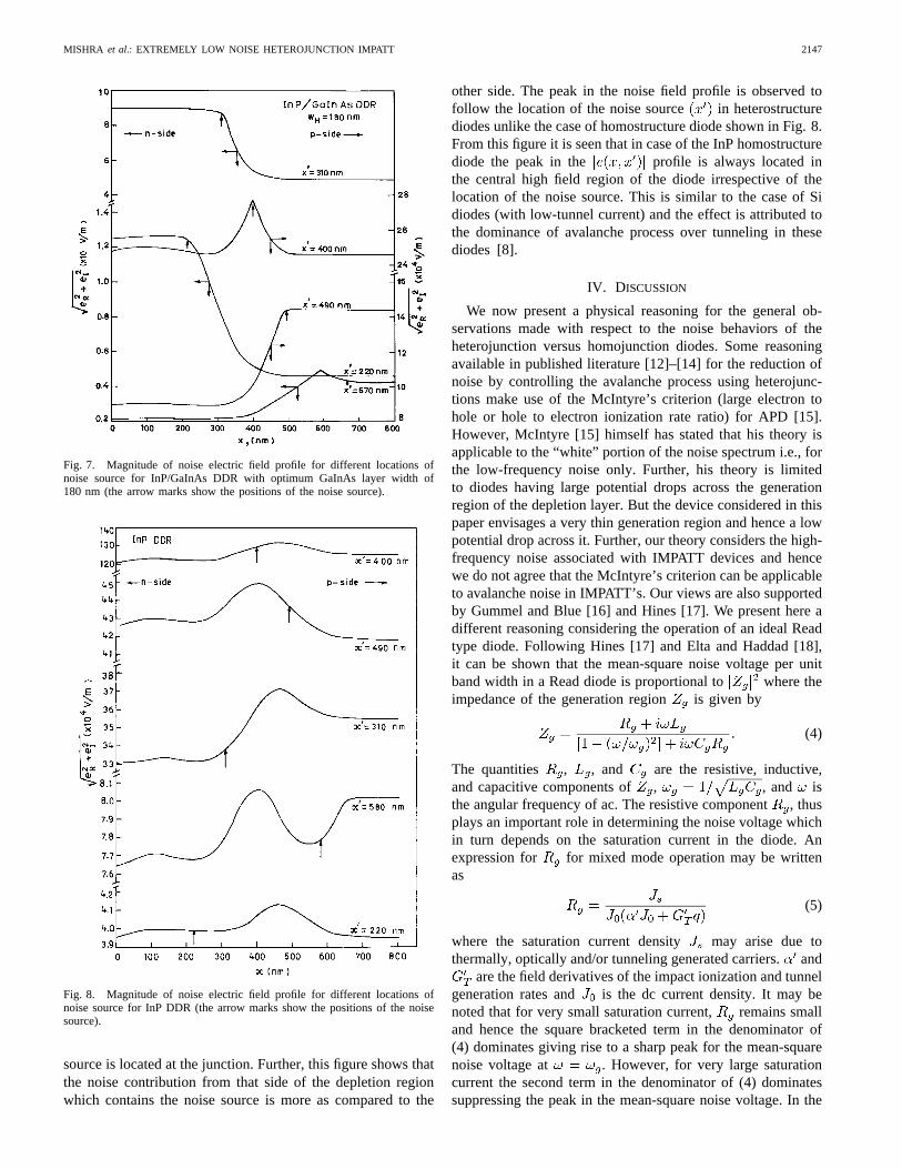
MISHRA et al.: EXTREMELY LOW NOISE HETEROJUNCTION IMPATT 2147
Fig. 7. Magnitude of noise electric field profile for different locations ofnoise source for InP/GaInAs DDR with optimum GaInAs layer width of180 nm (the arrow marks show the positions of the noise source).
Fig. 8. Magnitude of noise electric field profile for different locations ofnoise source for InP DDR (the arrow marks show the positions of the noisesource).
source is located at the junction. Further, this figure shows thatthe noise contribution from that side of the depletion regionwhich contains the noise source is more as compared to the
other side. The peak in the noise field profile is observed tofollow the location of the noise source in heterostructurediodes unlike the case of homostructure diode shown in Fig. 8.From this figure it is seen that in case of the InP homostructurediode the peak in the profile is always located inthe central high field region of the diode irrespective of thelocation of the noise source. This is similar to the case of Sidiodes (with low-tunnel current) and the effect is attributed tothe dominance of avalanche process over tunneling in thesediodes [8].
IV. DISCUSSION
We now present a physical reasoning for the general ob-servations made with respect to the noise behaviors of theheterojunction versus homojunction diodes. Some reasoningavailable in published literature [12]–[14] for the reduction ofnoise by controlling the avalanche process using heterojunc-tions make use of the McIntyre’s criterion (large electron tohole or hole to electron ionization rate ratio) for APD [15].However, McIntyre [15] himself has stated that his theory isapplicable to the “white” portion of the noise spectrum i.e., forthe low-frequency noise only. Further, his theory is limitedto diodes having large potential drops across the generationregion of the depletion layer. But the device considered in thispaper envisages a very thin generation region and hence a lowpotential drop across it. Further, our theory considers the high-frequency noise associated with IMPATT devices and hencewe do not agree that the McIntyre’s criterion can be applicableto avalanche noise in IMPATT’s. Our views are also supportedby Gummel and Blue [16] and Hines [17]. We present here adifferent reasoning considering the operation of an ideal Readtype diode. Following Hines [17] and Elta and Haddad [18],it can be shown that the mean-square noise voltage per unitband width in a Read diode is proportional to where theimpedance of the generation region is given by
(4)
The quantities , , and are the resistive, inductive,and capacitive components of , , and isthe angular frequency of ac. The resistive component, thusplays an important role in determining the noise voltage whichin turn depends on the saturation current in the diode. Anexpression for for mixed mode operation may be writtenas
(5)
where the saturation current density may arise due tothermally, optically and/or tunneling generated carriers.and
are the field derivatives of the impact ionization and tunnelgeneration rates and is the dc current density. It may benoted that for very small saturation current, remains smalland hence the square bracketed term in the denominator of(4) dominates giving rise to a sharp peak for the mean-squarenoise voltage at . However, for very large saturationcurrent the second term in the denominator of (4) dominatessuppressing the peak in the mean-square noise voltage. In the

2148 IEEE TRANSACTIONS ON ELECTRON DEVICES, VOL. 44, NO. 12, DECEMBER 1997
case of heterostructure IMPATT the saturation current risesdue to rise in thermal as well as tunneling components andhence the mean-square noise voltage is reduced. A furthercondition for low noise, as seen from (5), is to select theavalanche zone material and the field range such thatand
are low giving rise to a large . It may however beremembered that a large dissipates more power in theavalanche zone thereby reducing power output. Thus, theheterostructure IMPATT’s may find application as low-power,low-noise, and high-efficiency devices.
REFERENCES
[1] J. C. De Jaeger, R. Kozlowski, and G. Salmer, “High efficiencyGaInAs/InP heterojunction IMPATT diodes,”IEEE Trans. ElectronDevices, vol. ED-30, pp. 790–796, July 1983.
[2] R. U. Khan, P. Chakravarty, and B. B. Pal, “MITATT mode in DDRheterostructure IMPATT,”Appl. Phys. A, vol. 42, no. 4, pp. 303–309,1987.
[3] G. N. Dash and S. P. Pati, “Computer aided studies on the microwavecharacteristics of InP/GaInAs and GaAs/GaInAs heterostructure singledrift region impact avalanche transit time diodes,”J. Phys. D: Appl.Phys., vol. 27, pp. 1719–1726, 1994.
[4] , “Studies on the prospects of GaInAs and GaInAsP for doubledrift region heterostructure IMPATT’s,”Appl. Phys. A, vol. 58, pp.211–217, 1994.
[5] N. S. Dogan, J. R. East, M. Elta, and G. I. Haddad, “Millimeter-waveheterojunction MITATT diodes,”IEEE Trans. Microwave Theory Tech.,vol. MTT-35, pp. 1308–1315, Dec. 1987.
[6] M. J. Baily, “Heterojunction IMPATT diodes,”IEEE Trans. ElectronDevices, vol. 39, pp. 1829–1834, Aug. 1992.
[7] M. J. Kearney, N. R. Couch, J. Stephens, and R. S. Smith, “Heterostruc-ture impact avalanche transit time diodes grown by molecular beamepitaxy,” Semicond. Sci. Technol., vol. 8, p. 560, 1993.
[8] G. N. Dash, J. K. Mishra, and A. K. Panda, “Noise in mixed tunnelingavalanche transit time (MITATT) diodes,”Solid-State Electron., vol. 39,no. 10, pp. 1473–1479, 1996.
[9] F. Osaka and T. Mikawa, “Excess noise design of InP/GaInAsP/GaInAsavalanche photo diode,”IEEE J. Quantum Electron., vol. QE–22, p.471, 1986.
[10] S. M. Sze,Physics of Semiconductor Devices, 2nd ed. New York:Wiley, 1987.
[11] G. N. Dash and S. P. Pati, “A generalized simulation method forMITATT mode operation and studies on the influence of tunnel currenton IMPATT properties,”Semicond. Sci. Technol., vol. 7, pp. 222–230,1992.
[12] D. Lippens, J. L. Nieruchalski, and E. Constant, “Multi-layered hetero-junction structure for millimeter wave IMPATT devices,”Physica, vol.134B, pp. 72–76, 1985.
[13] A. Christou and K. Varmazis, “Superlattice GaAs mixed tunnelingavalanche transit time device structure,”Appl. Phys. Lett., vol. 48, p.1446, 1986.
[14] F. S. Barnes, W. H. Su, and K. F. Brennan, “A potential low-noiseavalanche diode microwave amplifier,”IEEE Trans. Electron Devices,vol. ED-34, p. 966, 1987.
[15] R. J. McIntyre, “Multiplication noise in uniform avalanche diode,”IEEETrans. Electron Devices, vol. ED-13, p. 164, 1966.
[16] H. K. Gummel and J. L. Blue, “A small signal theory of avalanchenoise in IMPATT diodes,”IEEE Trans. Electron Devices, vol. ED-14,p. 569, 1967.
[17] M. E. Hines, “Noise theory for the Read type avalanche diode,”IEEETrans. Electron Devices, vol. ED-13, pp. 158–163, 1966.
[18] M. E. Elta and G. I. Haddad, “Mixed tunneling and avalanche mech-anisms in p-n junctions and their effects on microwave transit-timedevices,”IEEE Trans. Electron Devices, vol. ED-25, pp. 694–702, 1978.
J. K. Mishra received the M.Sc. and M.Phil. de-grees in 1985 and 1988, respectively, from Sam-balpur University, Orissa, India, where he is cur-rently pursuing the Ph.D. degree.
In 1988, he became a Lecturer in physics underthe government of Orissa. Currently, he is serving asa Lecturer in physics at G. M. (Autonomous) Col-lege, Sambalpur, India. His current field of interestincludes solid-state electronic devices like IMPATT,MITATT, and APD.
A. K. Panda graduated from Sambalpur Univer-sity, Orissa, India, and, continuing his research inthe area of solid-state electronic devices with aUGC/CSIR fellowship, received the Ph.D. degreein 1997.
Since September 1996, he has been a memberof the faculty at the National Institute of Scienceand Technology, Berhampur University, Orissa. Hisfield of interest includes optimization of deviceproperties through neural networks and heterostruc-ture devices.
G. N. Dashwas born in 1955. He received the M.Sc.and M.Phil. degrees in physics and the Ph.D. de-gree in electronics, all from Sambalpur University,Orissa, India, in 1977, 1983, and 1992, respectively.
In 1978, he became a Lecturer in physics underthe government of Orissa. In 1984, he joined thephysics faculty of Sambalpur University, where heis currently serving as a Reader. He has publishedover 60 papers, including 20 in journals of interna-tional repute, in the field of solid-state electronics.His current research interests include theoretical
modeling and simulation of semiconductor devices for millimeter-wave andoptoelectronic applications.