an electron beam detector for the flash ii beam dump
TRANSCRIPT
Journal of Physics Conference Series
OPEN ACCESS
An electron beam detector for the FLASH II beamdumpTo cite this article J Good et al 2013 J Phys Conf Ser 425 122012
View the article online for updates and enhancements
You may also likePreparing topologically ordered states byHamiltonian interpolationXiaotong Ni Fernando Pastawski BeniYoshida et al
-
Design of the cryogenic system of thewideband phased array feed for QTTJun Ma Yang Wu Song Xiao et al
-
Investigation on Electron Absorbed Dosein a Mixture of Natural Rubber Latex andCross-linking AgentsP Nanthanasit P Jaikaew E Kongmon etal
-
This content was downloaded from IP address 911305616 on 31012022 at 2335
An electron beam detector for the FLASH II beam dump
J Good2 G Kube
1 N Leuschner
2 F Perlick
2 M Sachwitz
2 M Schmitz
1 K
Wittenburg1 and T Wohlenberg
1
1 DESY Hamburg site Notkestraszlige 85 22607 Hamburg Germany
2 DESY Zeuthen site Platanenallee 6 15738 Zeuthen Germany
E-mail florianperlickdesyde
Abstract After the generation of the laser light a dipole deflects the highly energetic electron
beam of the bdquoFree Electron Laser Hamburgldquo into a dump To control the position dimensions
and profile of the electron beam and to avoid contact with adjacent components causing a total
breakdown of the linac a detector is developed Light is emitted due to the electrons hitting a
luminescent screen and is then reflected by a mirror located in 2 m distance from the screen
and passes through a vacuum window to a CCD camera An experimental setup is currently
built representing quite closely the terms of installation at FLASH II In this setup the
ceramics Al2O3 and Chromox will be examined as screen materials
1 Introduction
The Free Electron Laser Hamburg (FLASH) is a linear accelerator producing brilliant laser light from
4 to 60 nm wavelengths providing unique experimental opportunities to investigate the atomic
structure and the properties of materials nanoparticles viruses and cells After the generation of the
laser light in the undulator sections the electrons are separated from the FEL beam While the laser
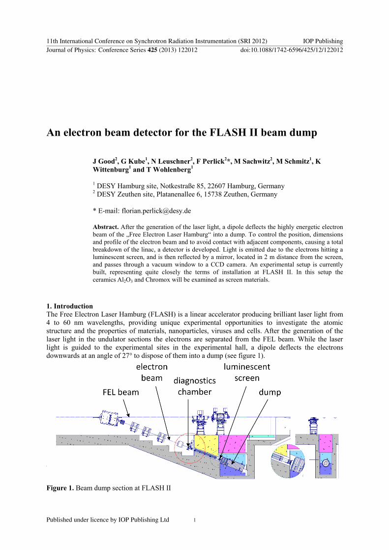
light is guided to the experimental sites in the experimental hall a dipole deflects the electrons
downwards at an angle of 27deg to dispose of them into a dump (see figure 1)
Figure 1 Beam dump section at FLASH II
11th International Conference on Synchrotron Radiation Instrumentation (SRI 2012) IOP PublishingJournal of Physics Conference Series 425 (2013) 122012 doi1010881742-659642512122012
Published under licence by IOP Publishing Ltd 1
The high power beam is able to easily damage beam line components in the case of misdirection
Therefore a detector is required at the dump to control the shape and the position of the beam The
detector will be surveyed continuously by the accelerator control room to immediately detect any
beam optic failures External coupling is not permitted due to the almost impossible
accessmaintenance at the termination of the beam pipe The detector has to be able to operate and
survive in a highly radioactive environment Therefore a luminescent screen 100 mm diameter in size
is installed in front of the dump aperture At a diagnostics chamber installed approximately in 2 m
distance from the screen the emitted light is reflected by a mirror through a vacuum window to a CCD
camera Since the camera is one of the components which have to be well protected from radiation it
is placed about one and a half meters away from the beam line shielded by the concrete at ground
level For guiding the light to the camera two different techniques will be applied redundantly In
addition to a conventional lens-mirror-system radiation-hard optical fibres will be used The entire
optical system is supposed to have a resolution better than 1 mm During the operation of FLASH II
the beam is expected in the middle of the screen Beam misdirection towards the screen edges will first
lead to an alarm signal and if the beam is outside the screen where it is invisible for the CCD FLASH
will be shut down immediately to avoid potential damage
2 Experimental setup
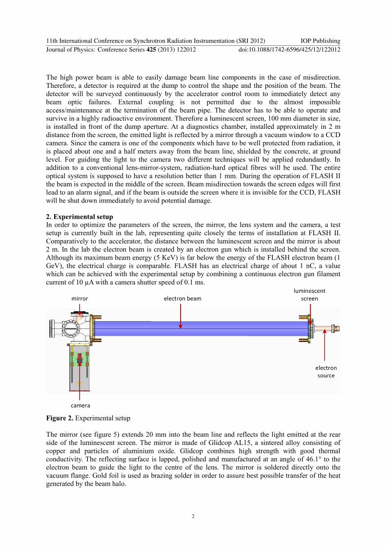
In order to optimize the parameters of the screen the mirror the lens system and the camera a test
setup is currently built in the lab representing quite closely the terms of installation at FLASH II
Comparatively to the accelerator the distance between the luminescent screen and the mirror is about
2 m In the lab the electron beam is created by an electron gun which is installed behind the screen
Although its maximum beam energy (5 KeV) is far below the energy of the FLASH electron beam (1
GeV) the electrical charge is comparable FLASH has an electrical charge of about 1 nC a value
which can be achieved with the experimental setup by combining a continuous electron gun filament
current of 10 microA with a camera shutter speed of 01 ms
Figure 2 Experimental setup
The mirror (see figure 5) extends 20 mm into the beam line and reflects the light emitted at the rear
side of the luminescent screen The mirror is made of Glidcop AL15 a sintered alloy consisting of
copper and particles of aluminium oxide Glidcop combines high strength with good thermal
conductivity The reflecting surface is lapped polished and manufactured at an angle of 461deg to the
electron beam to guide the light to the centre of the lens The mirror is soldered directly onto the
vacuum flange Gold foil is used as brazing solder in order to assure best possible transfer of the heat
generated by the beam halo
11th International Conference on Synchrotron Radiation Instrumentation (SRI 2012) IOP PublishingJournal of Physics Conference Series 425 (2013) 122012 doi1010881742-659642512122012
2
Figure 3 Glidcop mirror
3 Estimation of mirror temperature due to heat input
Since the possibility cannot be ignored that electrons of the beam halo may hit the mirror a thermal
simulation was made to get a rough estimate of the resulting mirror temperatures At FLASH the
average energy input into a material per beam train is about 12 1020
eVgcm-sup2 According to the
installation conditions of the mirror the maximum depth of impression into the Glidcop (density ca
8900 gcm3) is approximately 15 cm Considering the FLASH frequency of 10 Hz the resulting
thermal power the mirror has to deal with can be up to 2570 W
To optimize the heat transfer from the flange to the environment cooling fins were machined into it
For the simulation the boundary conditions at the mirror illustrate a worst case scenario The heat
transfer to the diagnostics chamber is restricted so the flange is the only part where convection is
possible (see figure 4) The estimated film coefficient of 5 Wm2K represents restrained convection
ie due to stagnant air and a flange contaminated with settled dust The ambient temperature in the
dump region was presumed to be 30degC
Figure 4 Boundary Conditions (simulation) Figure 5 Temperatures of mirror and flange
11th International Conference on Synchrotron Radiation Instrumentation (SRI 2012) IOP PublishingJournal of Physics Conference Series 425 (2013) 122012 doi1010881742-659642512122012
3
For the first simulation only 1 of the possible thermal beam power (257 W) is applied evenly to the
mirror on the blue surface (see figure 4) The mirror reaches up to 130degC while the maximum
temperature of the flange is about 110degC (see figure 5) Another simulation where the beam hits the
mirror at a small selected point at the top of the mirror (1 mm diameter) shows that around the point
of impact the mirror reaches a temperature of up to 212degC while the overall temperatures of the mirror
and the flange are similar to the previous simulation The last simulation where 10 of the thermal
beam power is applied to the Glidcop results in a maximum temperature of 1030degC at the top of the
mirror and 820degC at the outer face of the flange These temperatures are far too high so that in this
case the cooling system has to be significantly improved
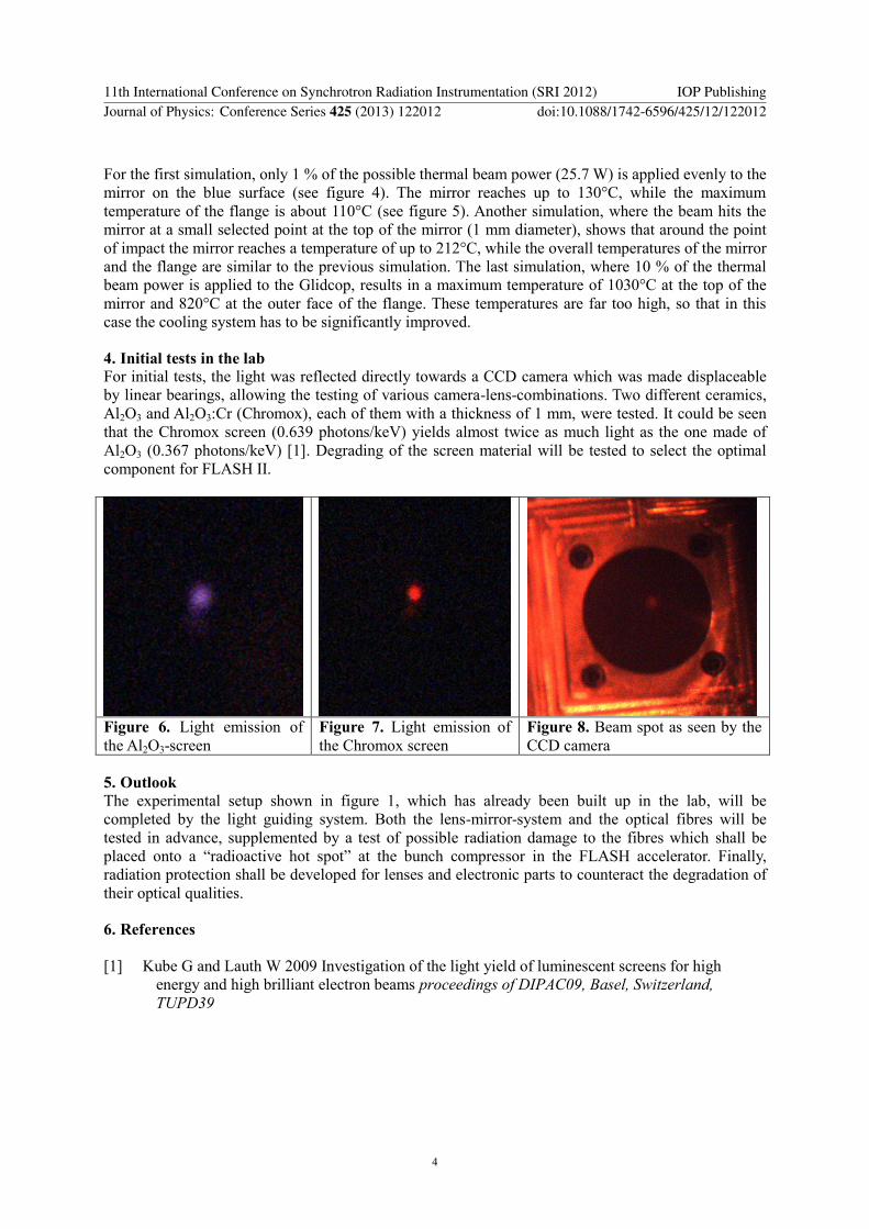
4 Initial tests in the lab
For initial tests the light was reflected directly towards a CCD camera which was made displaceable
by linear bearings allowing the testing of various camera-lens-combinations Two different ceramics
Al2O3 and Al2O3Cr (Chromox) each of them with a thickness of 1 mm were tested It could be seen
that the Chromox screen (0639 photonskeV) yields almost twice as much light as the one made of
Al2O3 (0367 photonskeV) [1] Degrading of the screen material will be tested to select the optimal
component for FLASH II
Figure 6 Light emission of
the Al2O3-screen
Figure 7 Light emission of
the Chromox screen
Figure 8 Beam spot as seen by the
CCD camera
5 Outlook
The experimental setup shown in figure 1 which has already been built up in the lab will be
completed by the light guiding system Both the lens-mirror-system and the optical fibres will be
tested in advance supplemented by a test of possible radiation damage to the fibres which shall be
placed onto a ldquoradioactive hot spotrdquo at the bunch compressor in the FLASH accelerator Finally
radiation protection shall be developed for lenses and electronic parts to counteract the degradation of
their optical qualities
6 References
[1] Kube G and Lauth W 2009 Investigation of the light yield of luminescent screens for high
energy and high brilliant electron beams proceedings of DIPAC09 Basel Switzerland
TUPD39
11th International Conference on Synchrotron Radiation Instrumentation (SRI 2012) IOP PublishingJournal of Physics Conference Series 425 (2013) 122012 doi1010881742-659642512122012
4
An electron beam detector for the FLASH II beam dump
J Good2 G Kube
1 N Leuschner
2 F Perlick
2 M Sachwitz
2 M Schmitz
1 K
Wittenburg1 and T Wohlenberg
1
1 DESY Hamburg site Notkestraszlige 85 22607 Hamburg Germany
2 DESY Zeuthen site Platanenallee 6 15738 Zeuthen Germany
E-mail florianperlickdesyde
Abstract After the generation of the laser light a dipole deflects the highly energetic electron
beam of the bdquoFree Electron Laser Hamburgldquo into a dump To control the position dimensions
and profile of the electron beam and to avoid contact with adjacent components causing a total
breakdown of the linac a detector is developed Light is emitted due to the electrons hitting a
luminescent screen and is then reflected by a mirror located in 2 m distance from the screen
and passes through a vacuum window to a CCD camera An experimental setup is currently
built representing quite closely the terms of installation at FLASH II In this setup the
ceramics Al2O3 and Chromox will be examined as screen materials
1 Introduction
The Free Electron Laser Hamburg (FLASH) is a linear accelerator producing brilliant laser light from
4 to 60 nm wavelengths providing unique experimental opportunities to investigate the atomic
structure and the properties of materials nanoparticles viruses and cells After the generation of the
laser light in the undulator sections the electrons are separated from the FEL beam While the laser
light is guided to the experimental sites in the experimental hall a dipole deflects the electrons
downwards at an angle of 27deg to dispose of them into a dump (see figure 1)
Figure 1 Beam dump section at FLASH II
11th International Conference on Synchrotron Radiation Instrumentation (SRI 2012) IOP PublishingJournal of Physics Conference Series 425 (2013) 122012 doi1010881742-659642512122012
Published under licence by IOP Publishing Ltd 1
The high power beam is able to easily damage beam line components in the case of misdirection
Therefore a detector is required at the dump to control the shape and the position of the beam The
detector will be surveyed continuously by the accelerator control room to immediately detect any
beam optic failures External coupling is not permitted due to the almost impossible
accessmaintenance at the termination of the beam pipe The detector has to be able to operate and
survive in a highly radioactive environment Therefore a luminescent screen 100 mm diameter in size
is installed in front of the dump aperture At a diagnostics chamber installed approximately in 2 m
distance from the screen the emitted light is reflected by a mirror through a vacuum window to a CCD
camera Since the camera is one of the components which have to be well protected from radiation it
is placed about one and a half meters away from the beam line shielded by the concrete at ground
level For guiding the light to the camera two different techniques will be applied redundantly In
addition to a conventional lens-mirror-system radiation-hard optical fibres will be used The entire
optical system is supposed to have a resolution better than 1 mm During the operation of FLASH II
the beam is expected in the middle of the screen Beam misdirection towards the screen edges will first
lead to an alarm signal and if the beam is outside the screen where it is invisible for the CCD FLASH
will be shut down immediately to avoid potential damage
2 Experimental setup
In order to optimize the parameters of the screen the mirror the lens system and the camera a test
setup is currently built in the lab representing quite closely the terms of installation at FLASH II
Comparatively to the accelerator the distance between the luminescent screen and the mirror is about
2 m In the lab the electron beam is created by an electron gun which is installed behind the screen
Although its maximum beam energy (5 KeV) is far below the energy of the FLASH electron beam (1
GeV) the electrical charge is comparable FLASH has an electrical charge of about 1 nC a value
which can be achieved with the experimental setup by combining a continuous electron gun filament
current of 10 microA with a camera shutter speed of 01 ms
Figure 2 Experimental setup
The mirror (see figure 5) extends 20 mm into the beam line and reflects the light emitted at the rear
side of the luminescent screen The mirror is made of Glidcop AL15 a sintered alloy consisting of
copper and particles of aluminium oxide Glidcop combines high strength with good thermal
conductivity The reflecting surface is lapped polished and manufactured at an angle of 461deg to the
electron beam to guide the light to the centre of the lens The mirror is soldered directly onto the
vacuum flange Gold foil is used as brazing solder in order to assure best possible transfer of the heat
generated by the beam halo
11th International Conference on Synchrotron Radiation Instrumentation (SRI 2012) IOP PublishingJournal of Physics Conference Series 425 (2013) 122012 doi1010881742-659642512122012
2
Figure 3 Glidcop mirror
3 Estimation of mirror temperature due to heat input
Since the possibility cannot be ignored that electrons of the beam halo may hit the mirror a thermal
simulation was made to get a rough estimate of the resulting mirror temperatures At FLASH the
average energy input into a material per beam train is about 12 1020
eVgcm-sup2 According to the
installation conditions of the mirror the maximum depth of impression into the Glidcop (density ca
8900 gcm3) is approximately 15 cm Considering the FLASH frequency of 10 Hz the resulting
thermal power the mirror has to deal with can be up to 2570 W
To optimize the heat transfer from the flange to the environment cooling fins were machined into it
For the simulation the boundary conditions at the mirror illustrate a worst case scenario The heat
transfer to the diagnostics chamber is restricted so the flange is the only part where convection is
possible (see figure 4) The estimated film coefficient of 5 Wm2K represents restrained convection
ie due to stagnant air and a flange contaminated with settled dust The ambient temperature in the
dump region was presumed to be 30degC
Figure 4 Boundary Conditions (simulation) Figure 5 Temperatures of mirror and flange
11th International Conference on Synchrotron Radiation Instrumentation (SRI 2012) IOP PublishingJournal of Physics Conference Series 425 (2013) 122012 doi1010881742-659642512122012
3
For the first simulation only 1 of the possible thermal beam power (257 W) is applied evenly to the
mirror on the blue surface (see figure 4) The mirror reaches up to 130degC while the maximum
temperature of the flange is about 110degC (see figure 5) Another simulation where the beam hits the
mirror at a small selected point at the top of the mirror (1 mm diameter) shows that around the point
of impact the mirror reaches a temperature of up to 212degC while the overall temperatures of the mirror
and the flange are similar to the previous simulation The last simulation where 10 of the thermal
beam power is applied to the Glidcop results in a maximum temperature of 1030degC at the top of the
mirror and 820degC at the outer face of the flange These temperatures are far too high so that in this
case the cooling system has to be significantly improved
4 Initial tests in the lab
For initial tests the light was reflected directly towards a CCD camera which was made displaceable
by linear bearings allowing the testing of various camera-lens-combinations Two different ceramics
Al2O3 and Al2O3Cr (Chromox) each of them with a thickness of 1 mm were tested It could be seen
that the Chromox screen (0639 photonskeV) yields almost twice as much light as the one made of
Al2O3 (0367 photonskeV) [1] Degrading of the screen material will be tested to select the optimal
component for FLASH II
Figure 6 Light emission of
the Al2O3-screen
Figure 7 Light emission of
the Chromox screen
Figure 8 Beam spot as seen by the
CCD camera
5 Outlook
The experimental setup shown in figure 1 which has already been built up in the lab will be
completed by the light guiding system Both the lens-mirror-system and the optical fibres will be
tested in advance supplemented by a test of possible radiation damage to the fibres which shall be
placed onto a ldquoradioactive hot spotrdquo at the bunch compressor in the FLASH accelerator Finally
radiation protection shall be developed for lenses and electronic parts to counteract the degradation of
their optical qualities
6 References
[1] Kube G and Lauth W 2009 Investigation of the light yield of luminescent screens for high
energy and high brilliant electron beams proceedings of DIPAC09 Basel Switzerland
TUPD39
11th International Conference on Synchrotron Radiation Instrumentation (SRI 2012) IOP PublishingJournal of Physics Conference Series 425 (2013) 122012 doi1010881742-659642512122012
4
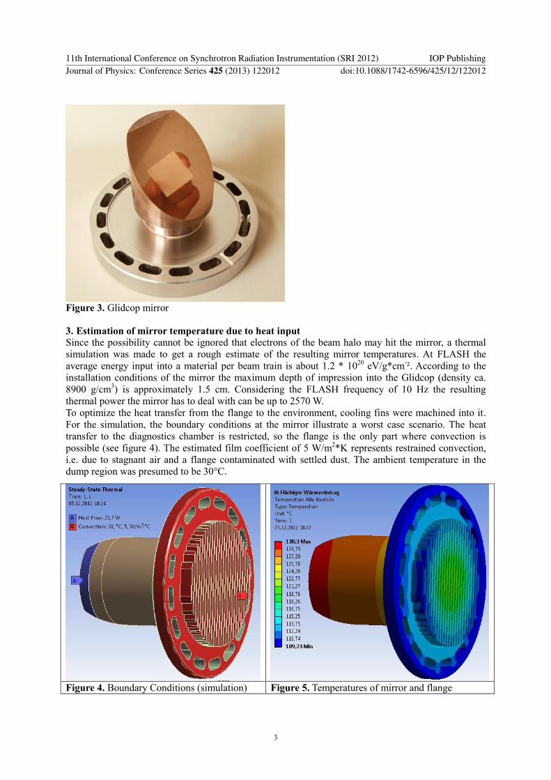