an 550: using the dll phase offset feature in stratix fpgas and … · 2020-01-20 · phase...
TRANSCRIPT

© March 2010 Altera Corporation
© March 2010
AN 550: Using the DLL Phase OffsetFeature in Stratix FPGAs and
HardCopy ASICs
AN-550-2.0This application note describes how to implement the delay-locked loop (DLL) phaseoffset feature with Altera® Stratix® FPGAs and HardCopy® ASICs.
IntroductionA DLL provides a process, voltage, and temperature (PVT)-compensated delay thatyou can use to phase shift the read clock from an external memory to align it with thecenter of the data valid window. The DLL phase offset feature provides a method tomake fine non-PVT-compensated phase adjustments to the read clock from anexternal memory. If the circuit board or memory timing specifications are differentthan expected, you can use the DLL phase offset feature to optimize the read capturetiming.
This application note contains examples of changing the phase offset when you areusing one of the following MegaCore® functions or megafunctions:
■ DDR3/DDR2/DDR High Performance controller
■ DDR2 Legacy Integrated Static Data Path and Controller for HardCopy II ASICs(referred to as the Legacy Static PHY)
■ ALTMEMPHY megafunction
■ ALTDQS megafunction
Included in this application note are example files that show how to implement a DLLphase offset with the ALTMEMPHY megafunction and Legacy Static PHY.
This application note contains the following sections:
■ “DLL Overview” on page 1
■ “DLL Phase Offset Control” on page 2
■ “Using TimeQuest’s set_annotated_delay to Analyze the Effect of the DLL PhaseOffset Feature” on page 5
■ “Using DLL Phase Offset with the ALTMEMPHY Megafunction” on page 7
■ “Instantiating a DLL with Altera IP” on page 8
■ “Confirm Your DLL Phase Offset Control Settings” on page 29
DLL OverviewAltera’s external memory interface read capture logic is composed of the DLL and itsphase offset control block, the DQS logic block, and the DQ blocks. The DLLautomatically adjusts its delay chains to have a delay equal to one cycle of its inputclock.
AN 550: Using the DLL Phase Offset Feature in Stratix FPGAs and HardCopy ASICs

Page 2 DLL Phase Offset Control
The DLL outputs a value on the delayctrlout bus based on its phase shift setting.Thedelayctrloutbus goes to the phase offset control block and to the DQS blocks.In the DQS blocks, the value on delayctrlout selects the number of delay buffersused to phase shift the read clock from memory. In the phase offset control block, thevalue on the bus offset is added to or subtracted fromdelayctrlout, depending onthe addnsub signal. This value, called offsetctrlout, goes to the DQS blocks andselects the number of delay buffers in only one of the four DQS delay chains.
Figure 1 shows an overview of the DLL/DQS logic block for all Stratix and HardCopyseries devices.
DLL Phase Offset ControlThe DLL phase offset feature allows you to add or subtract a non-PVT-compensatedoffset to the DQS phase shift that is used to capture read data inside the device.Depending on the HardCopy device used, each DLL has one or two phase offsetmodules that can provide DQS delay settings with an independent offset, so you canfine-tune the DQS phase shift settings.
Figure 1. DLL/DQS Logic Block for Stratix and HardCopy Devices
6
6
PhaseOffsetControl
6
Phase OffsetSettings from theLogic Array
Phase Offset Settings
InputReference
Clock
upndn
clock enable
DLL6
addnsub
PhaseComparator
Delay Chains
Up/DownCounter
D QD Q
ENENUpdateEnable
Circuitry
66 66
6 6
DQS DelaySettings to and from the
Logic Array
DQS DelaySettings from theDQS Phase-Shift
Circuitry
DQS orCQ
DQS DelayChain
Bypass
DQS Logic Block
DQS Logic Block
DQS Logic Block
DQS Phase-ShiftCircuitry
DQS orCQ
DQS or DQSn
NOT
Postamble Circuitrygated_dqs control
DQS bus
PRNQ
reset
EnableNAB VCC
DQS'
SCLR
Mux Selection EnablingPhase Offsetting
offsetctrlout
The only delay chain adjusted by phase offsetting if the feature isenabled
delayctrlout
DFF
CLRN
AN 550: Using the DLL Phase Offset Feature in Stratix FPGAs and HardCopy ASICs © March 2010 Altera Corporation

DLL Phase Offset Control Page 3
If you find bit errors in the HardCopy ASIC DDR interface as a result of a change tothe board design (which changes board latency) or to the memory vendor’s originalspecification, you can fine tune the DQS phase shift to accommodate the changes. Forexample, if a 90° DQS phase shifted DQ read capture is generating intermittent biterrors in corner-case conditions of operating temperature and/or voltage, a firmwarechange on the device could adjust the phase shift to a new value (for example, 85°)that would allow the device to properly capture the DDR read data. The main settingsof the DLL do not allow a phase shift of 85°. Using the DLL phase offset feature allowsfor fine tuning the phase shift.
Figure 2 shows how the DQS inside a device changes with offset adjustment.
1 The proximity of the edge without offset adjustment to the data changing isexaggerated for the purpose of illustration.
The DLL phase offset is controlled by two signals, addnsub and offset[5:0]. Theaddnsub signal controls whether the value on offset[5:0] is added to orsubtracted from the default delay value. You can control the values of addnsub andoffset[5:0] in a variety of ways. For example, they can be controlled by anaddressable port in a microprocessor’s address space, by part of a scan chain thatcontrols PLL reconfiguration, or by connecting directly to pins that are connected to adual in-line package (DIP) switch. Another method of controlling phase offset is touse In-System Sources and Probes. You can drive the addnsub and offset[5:0]signals and you can monitor delayctrlout[5:0].
f For more information about In-System Sources and Probes, refer to the DesignDebugging Using In-System Sources and Probes chapter in volume 3 of the Quartus IIHandbook.
When addnsub is high, the value specified in offset[5:0]multiplied by the delayin Table 2 on page 4 is included as additional uncompensated delay to the DQS phaseshift. When addnsub is low, its 2’s complement (!offset[5:0] +1) multiplied bythe delay in Table 2 on page 4 is subtracted from the DQS phase shift (for example, tosubtract 1, set offset to 111111).
Figure 2. DQS Inside Device With and Without Phase Adjustment
DQ data at input register
DLL shifted DQS strobe arrivalat the DQ capture register
DQS with offset adjustment
© March 2010 Altera Corporation AN 550: Using the DLL Phase Offset Feature in Stratix FPGAs and HardCopy ASICs

Page 4 DLL Phase Offset Control
It might be easier to think of {!addnsub,offset[5:0]} as a 7-bit 2’s complementvalue for the offset with the sign bit, addnsub, inverted. To add 11 (decimal), setaddnsub to 1 and offset[5:0] to 001011. To subtract 9, set addnsub to zero. Foroffset[5:0], take 9 (001001), its ones complement is 110110. Its 2’s complement is110110 + 1 = 110111.
Table 1 lists the frequency modes, frequency ranges, and the number of delay chainsused in Stratix II FPGAs and HardCopy II ASICs.
f For frequency modes, ranges, and delay chains of Stratix III, Stratix IV, HardCopy III,and HardCopy IV devices, refer to the DC and Switching Characteristics chapter in theirrespective handbooks.
Table 2 lists the allowable DQS offset delay per stage for the various device speedgrades for Stratix II FPGAs. The valid offset[] ranges are –64 to +63 when youconfigure the DLL and DQS delay buffers in low frequency mode (DLL frequencymode 0) and –32 to +31 when you configure the DLL and DQS delay buffers in highfrequency mode (DLL frequency modes 1, 2, and 3).
f For the DQS phase offset delay per stage for Stratix III, Stratix IV, and HardCopy IIIdevices, refer to the DC and Switching Characteristics chapter in their respectivehandbooks.
The following example is based on the DQS phase offset delay per stage for Stratix IIFPGAs. You can use the same method for Stratix III and Stratix IV FPGAs andHardCopy III and HardCopy IV ASICs. If you are using frequency mode 1 for a200-MHz DDR interface and the DQS DLL is set to 90°, and you want to shift the DQSto 85° to add an additional 5° of hold time margin, perform the following steps todetermine the setting:
1. For a frequency of 200 MHz, the period is 5 ns, or 5,000 ps. The delay (inps-per-degree) = 5000 ps/360 degrees = 13.88 ps/degree. Because you want toshift the DQS by 5°, 5 degrees × 13.88 ps/degree = 69.4 ps.
Table 1. Frequency Modes, Ranges, and Delay Chains for –4 Speed Grade of Stratix II FPGAs and HardCopy II ASICs
Frequency Mode Frequency Range (MHz) Available Phase Shift Number of Delay Chains
0 100 to 175 30, 60, 90, 120 12
1 150 to 230 22.5, 45, 67.5, 90 16
2 200 to 310 30, 60, 90, 120 12
3 240 to 350 36, 72, 108, 144 10
Table 2. DQS Phase Offset Delay Per Stage for Stratix II FPGAs (Note 1), (2)
Speed Grade Minimum Maximum Unit
–3 9 14 ps
–4 9 14 ps
–5 9 15 ps
Notes to Table 2:(1) The delay settings are linear.(2) The typical value equals the average of the minimum and maximum values.
AN 550: Using the DLL Phase Offset Feature in Stratix FPGAs and HardCopy ASICs © March 2010 Altera Corporation

Using TimeQuest’s set_annotated_delay to Analyze the Effect of the DLL Phase Offset Feature Page 5
2. To achieve a shift of 69.4 ps, divide 69.4 by the average of the minimum andmaximum delay per stage, which is 11.5. This gives you 6.03 (round to 6). The 2’scomplement of 6 is the ones complement plus one, so 6 = 000110, its onescomplement is 111001 and its 2’s complement is 111001+1, which is 111010.
3. Set addnsub low and set offset [5:0] = 111010. Setting offset[5:0] to the 2’scomplement of 6 reduces the delay in the range of 9 × 6 = 54 ps to 14 × 6 = 84 ps ina –3 or –4 Stratix II FPGA. It is in the same range for a HardCopy II ASIC.
The DLL makes a determination of what the delay settings must be to achieve therequested phase shift at the capture register. For example, if you set a phase shift of30°, the DLL might produce a delay setting of 28. This is the number of delay buffersto use in the delay chains. In this case, you cannot subtract more than 28 using theDLL phase offset feature. Doing so produces a delay setting that selects fewer thanzero delay buffers, which is physically impossible.
The DQS delay buffer also has a maximum setting that depends on the DLL’sdelayctrlout output; the offset is added to the DLL’sdelayctrlout, so the offsetcannot be greater than the maximum setting (+63 for DLL frequency mode 0 and +31for DLL frequency modes 1, 2, and 3) minus the delayctrlout setting. The portdelayctrlout[5:0] can be connected to your logic so that you can observe itsvalue in order to determine the values that can be used for the offset. The value ondelayctrlout[5:0] is not static; it can vary with changes in voltage andtemperature. Using the value on delayctrlout[5:0] allows you to calculate themaximum value you can effectively use onoffset[5:0]. Altera recommends usinga mode for which the frequency is closer to the middle of the range rather than closerto the end of the range. This allows the most adjustment range to add or subtractdelay. For example, if your frequency is 200 MHz, mode 1 is a better choice thanmode 2.
f For more information about frequency ranges, refer to the “DLL Frequency RangeSpecifications” table in the DC and Switching Characteristics chapter in volume 1 of theStratix II Device Handbook.
Using TimeQuest’s set_annotated_delay to Analyze the Effect of theDLL Phase Offset Feature
Use the TimeQuest Timing Analyzer to annotate the delay between two adjacentpoints on a path. To analyze timing, first calculate the offset value. Report the timingat the slow operating condition from the DQS pin to *. Here is the TimeQuest TimingAnalyzer command:
report_path -from [get_ports [mem_dqs[0]]] -to * -npaths 10 \-panel_name {Report Path}
Figure 3 shows an example of a situation that requires an earlier shift capture.
© March 2010 Altera Corporation AN 550: Using the DLL Phase Offset Feature in Stratix FPGAs and HardCopy ASICs

Page 6 Using TimeQuest’s set_annotated_delay to Analyze the Effect of the DLL
In the example shown in Figure 3, refer to the DQS phase offset delay values (Table 2)and shift the capture point 5° earlier. Use the following procedure to calculate theoffset value (in ns):
1. Set the operating conditions to slow:
a. Calculate the minimum delay:
1.125 – (5 × 0.014) = 1.055
b. Calculate the maximum delay:
1.125 – (5 × 0.009) = 1.080
2. Set the new delay that includes the offset for slow conditions:
set_annotated_delay -max 1.080 -min 1.055 \-from *g_datapath:*:g_ddr_io|dqs_io~comb_dqs \-to *g_datapath:*:g_ddr_io|dqsbusout -rr -ff
3. Report timing at the slow conditions.
4. Set the operating conditions to fast. Assume the delay at the fast operatingcondition is 0.563, then:
a. Calculate the maximum delay:
0.563 – (5 × 0.009) = 0.518
b. Calculate the minimum delay:
0.563 – (5 × 0.014) = 0.493
5. Set the new delay that includes the offset for the fast conditions:
set_annotated_delay -max 0.518 -min 0.493 \-from *g_datapath:*:g_ddr_io|dqs_io~comb_dqs \-to *g_datapath:*:g_ddr_io|dqsbusout -rr -ff
6. Report timing at the fast conditions.
Figure 3. Example of a Situation that Requires the Shift Capture Point 5° Earlier
AN 550: Using the DLL Phase Offset Feature in Stratix FPGAs and HardCopy ASICs © March 2010 Altera Corporation

Using DLL Phase Offset with the ALTMEMPHY Megafunction Page 7
Using DLL Phase Offset with the ALTMEMPHY MegafunctionThe system block diagram in Figure 4 shows how the DLL, ALTMEMPHYmegafunction, and user logic interact.
Figure 4. DLL Phase Offset System View
.
PLL Reconfig
Block
PLL
uSeq
ALTMEMPHY Megafunction
Reset Logic
Clock Crossing Control Logic
User IP DLL
Phase
Interface
User IP Logic
User IP
ClockLogic
DLL
Offset
soft_reset_n
global_reset_n
offset [5:0],addnsub
delayctrlout[5:0]
phy_internal_reset
reset_request_n
dll_reconfig_clk
user_ip_clock pll_ref_clk
pll_reset
pll_locked
dll_ref_clk
© March 2010 Altera Corporation AN 550: Using the DLL Phase Offset Feature in Stratix FPGAs and HardCopy ASICs

Page 8 Instantiating a DLL with Altera IP
Figure 5 shows the sequence you must follow after changing the DLL phase offset.
Instantiating a DLL with Altera IPThere are three ways to instantiate a DLL with Altera IP:
■ The most common way to instantiate a DLL with Altera IP is to use theALTMEMPHY megafunction. When using the ALTMEMPHY megafunction(Altera’s auto-calibrating DDR PHY), the DLL phase offset must be set beforecalibration. If the DLL phase offset is changed after calibration, you must reruncalibration.Tomaketherequiredconnections intheALTMEMPHYmegafunctionin the Quartus® II software version 8.1 and earlier, refer to “Making theConnections to Use the DLL Phase Offset Feature with the ALTMEMPHYMegafunction” on page 9. The DLL can be either an internal DLL or an externalDLL.
Figure 5. DLL Phase Offset Flow
Enable DLL Reconfig Option(ALTMEMPHY)
Assert soft_reset_nand hold during process
Change DLL Phase Offsetsetting (add or sub)
De-assert soft_reset_n(Reconfiguration Complete)
ALTMEMPHYcalibration restarts
AN 550: Using the DLL Phase Offset Feature in Stratix FPGAs and HardCopy ASICs © March 2010 Altera Corporation
Instantiating a DLL with Altera IP Page 9
■ You can instantiate a DLL with custom IP by using the ALTDQS megafunction.Use this method if you are designing a custom DDR PHY interface. When youmake the selections in the ALTDQS MegaWizard™ Plug-In Manager, it makes theconnections necessary for the DLL phase offset feature automatically. To make therequired connections using the ALTDQS megafunction, refer to“Instantiating theDLL Phase Offset Using the ALTDQS Megafunction” on page 22.
■ For HardCopy II ASICs, you can also instantiate a DLL with Altera IP by using theLegacy Static PHY. To make the connections between the DLL offset block and theDQS blocks in the Legacy Static PHY, refer to “Making the Connections to Use theDLL Phase Offset Feature with the Legacy Static PHY” on page 23.
The following sections contain step-by-step instructions for each of these methods.These instructions are valid for all Stratix FPGA device families.
Examples of the files that you must change to instantiate a DLL with Altera IP areavailable in the accompanying zip files. The lines that you must change are markedwith the comment //DLL_Phase_Offset.
You can find these example files on the Altera web site (www.altera.com), along withthis application note:
■ altmemphy_int_dll.zip—The zip file for the ALTMEMPHY megafunction withinternal DLL.
■ altmemphy_ext_dll.zip—The zip file for the ALTMEMPHY megafunction withexternal DLL.
■ static_dll.zip—The zip file for the Legacy Static PHY.
Making the Connections to Use the DLL Phase Offset Feature with the ALTMEMPHYMegafunction
The following examples describe the connections you must make in your design toimplement the DLL phase offset feature with the ALTMEMPHY megafunction for theQuartus II software version 8.1 and earlier. The first example gives instructions for anALTMEMPHY megafunction with an internal DLL. The second example givesinstructions for an external DLL, which you can use when the DLL is shared betweenALTMEMPHY megafunctions.
This demonstration design uses:
■ The filename myddr2 in the MegaWizard Plug-In Manager
■ The DDR2 SDRAM High Performance Controller version 8.0
■ The project name is myddr2_example_top
■ The top-level module is myddr2_example_top and is contained in themyddr2_example_top.v file
© March 2010 Altera Corporation AN 550: Using the DLL Phase Offset Feature in Stratix FPGAs and HardCopy ASICs

Page 10 Instantiating a DLL with Altera IP
Internal DLLFigure 6 shows a schematic block diagram for an ALTMEMPHY megafunction withan internal DLL.
1. In the myddr2_example_top.v file:
a. In the wire list before the first wire declaration, add these two lines:
wire addnsub;
wire [5:0] offset;
to make the connections from the DLL to your logic that controls the offsetfeature.
b. Connect those wires to pins or registers in your design to control the DLLphase offset feature.
Figure 6. ALTMEMPHY Megafunction with Internal DLL
CLK
ALOAD
OFFSET[5..0]
DELAYCTRLOUT[5..0]
OFFSETCTRLOUT[5..0]
dll
STRATIXII_DLL
myddr2_phy_alt_mem_phy:clk_reset_clk
DATAIN
DDIODATAIN
OE
OUTCLK
OUTCLKENA
INCLK
INCLKENA
ARESET
SRESET
DELAYCTRLIN[5..0]
OFFSETCTRLIN[5..0]
0
1
1
1
ADDNSUB
0
dqs[0].dqs_io
STRATIXII_IO
myddr2:myddr2_inst
myddr_controller_phy:myddr2_controller_phy_inst
myddr2_phy:alt_mem_phy_inst
myddr2_phy_alt_mem_phy:myddr2_phy_alt_mem_phy_inst
myddr2_phy_alt_mem_phy_dp_io:dpio
AN 550: Using the DLL Phase Offset Feature in Stratix FPGAs and HardCopy ASICs © March 2010 Altera Corporation

Instantiating a DLL with Altera IP Page 11
c. In the myddr2 myddr2_inst instantiation, in the port connection list, addthese two lines:
.addnsub(addnsub),
.offset(offset),
to create the top-level port connections and wires to these ports.
2. Because the MegaWizard Plug-In Manager controller filename you are using inyour example is myddr2, the Verilog file that you must modify is myddr2.v.
a. In the port list, add these two lines:
addnsub,
offset,
to create ports to connect addnsub and offset to the controller.
b. In the input declarations, add these two lines:
input addnsub;
input [5:0] offset;
to declare the ports addnsub and offset.
c. In the myddr2_controller_phy myddr2_controller_phy_instinstantiation, in the port connection list, add these two lines:
.addnsub(addnsub),
.offset(offset),
to create the top-level port connections and wires to these ports on thecontroller.
3. In the myddr2_controller_phy.v file:
a. In the port list, add these two lines:
addnsub,
offset,
to create ports to connect addnsub and offset to alt_mem_phy.
b. In the input declarations, add these two lines:
input addnsub;
input [5:0] offset;
to declare the ports addnsub and offset.
c. In themyddr2_phy alt_mem_phy_inst instantiation, in the port connectionlist, add these two lines:
.addnsub(addnsub),
.offset(offset),
to create the top-level port connections and wires to these ports onalt_mem_phy.
© March 2010 Altera Corporation AN 550: Using the DLL Phase Offset Feature in Stratix FPGAs and HardCopy ASICs

Page 12 Instantiating a DLL with Altera IP
4. In the myddr2_phy.v file:
a. In the port list, add these two lines:
addnsub,
offset,
to create ports to connect addnsub and offset.
b. In the input declarations, add these two lines:
input addnsub;
input [5:0] offset;
to declare the ports addnsub and offset.
c. In the myddr2_phy_alt_mem_phy_siimyddr2_phy_alt_mem_phy_sii_inst instantiation, in the port connectionlist, add these two lines:
.addnsub(addnsub),
.offset(offset),
to create the top-level port connections and wires to these ports.
5. In the myddr2_phy_alt_mem_phy_sii.v file:
a. In the port list in the section:
//DLL import/export ports :
add these three lines:
addnsub,
offset,
dqs_offset_ctrl_export,
to create ports to connect addnsub, offset, anddqs_offset_ctrl_export.
b. In the input and output declarations, add these three lines:
input wire addnsub;
input wire [5:0] offset;
output wire [DQS_DELAY_CTL_WIDTH - 1 : 0] \dqs_offset_ctrl_export;
to declare the ports addnsub, offset, and dqs_offset_ctrl_export.
c. After the line:
wire [DQS_DELAY_CTL_WIDTH - 1 : 0 ] \dqs_delay_ctrl_internal;
add these two lines:
wire [DQS_DELAY_CTL_WIDTH - 1 : 0 ] \dqs_offset_ctrl_internal;
AN 550: Using the DLL Phase Offset Feature in Stratix FPGAs and HardCopy ASICs © March 2010 Altera Corporation

Instantiating a DLL with Altera IP Page 13
wire [DQS_DELAY_CTL_WIDTH - 1 : 0 ] dqs_offset_ctrl;//Output from clk_reset block
to create wires to connect dqs_offset_ctrl_internal anddqs_offset_ctrl.
d. After the line:
assign dqs_delay_ctrl_internal = dqs_delay_ctrl;
add this line:
assign dqs_offset_ctrl_internal = dqs_offset_ctrl;
to connect dqs_offset_ctrl to dqs_offset_ctrl_internal.
e. After the line:
assign dqs_delay_ctrl_export = dqs_delay_ctrl;
add this line:
assign dqs_offset_ctrl_export = dqs_offset_ctrl;
to connect dqs_offset_ctrl to dqs_offset_ctrl_export.
f. In the myddr2_phy_alt_mem_phy_dp_io_sii module instantiation, afterthe line:
.dqs_delay_ctrl (dqs_delay_ctrl_internal),
add this line:
.dqs_offset_ctrl (dqs_offset_ctrl_internal),
to create the port and make the connection betweendqs_offset_ctrl_internal and dqs_offset_ctrl.
g. In the module instantiation:
myddr2_phy_alt_mem_phy_clk_reset_sii, after the line:
.dqs_delay_ctrl (dqs_delay_ctrl),
add these three lines:
.dqs_offset_ctrl (dqs_offset_ctrl),
.addnsub(addnsub),
.offset(offset),
to create the top-level port connections and wires to these ports.
h. In the module declaration:
module myddr2_phy_alt_mem_phy_dp_io_sii
after the line:
dqs_delay_ctrl,
add this line:
dqs_offset_ctrl,
to add the port dqs_offset_ctrl.
© March 2010 Altera Corporation AN 550: Using the DLL Phase Offset Feature in Stratix FPGAs and HardCopy ASICs

Page 14 Instantiating a DLL with Altera IP
i. In the input port declaration list, after the line:
input wire [DQS_DELAY_CTL_WIDTH - 1 : 0 ] \dqs_delay_ctrl;
add this line:
input wire [DQS_DELAY_CTL_WIDTH - 1 : 0 ] \dqs_offset_ctrl;
to declare the port dqs_offset_ctrl.
j. In the generate block that instantiates:
begin : dqs stratixii_io ... dqs_io
being careful not to change the block that has dq_io, change the line:
.dqs_offsetctrl_enable ("false"),
to:
.dqs_offsetctrl_enable ("true"),
after the line:
.delayctrlin (dqs_delay_ctrl),
change the line:
.offsetctrlin (),
to:
.offsetctrlin (dqs_offset_ctrl),
to make the connection of offsetctrlin to the DQS blocks.
k. In the module declaration:
module: myddr2_phy_alt_mem_phy_clk_reset_sii
in the port list, add these three lines:
dqs_offset_ctrl,
addnsub,
offset,
to add the ports dqs_offset_ctrl, addnsub, and offset.
l. In the instantiation:
myddr2_phy_alt_mem_phy_dp_io_sii ... ) dpio (
after the line:
.dqs_delay_ctrl (dqs_delay_ctrl_internal),
add this line:
.dqs_offset_ctrl (dqs_offset_ctrl_internal),
to create the port dqs_offset_ctrl and connectdqs_offset_ctrl_internal to it.
m. In the input declarations in the “Misc I/O” section, add these three lines:
AN 550: Using the DLL Phase Offset Feature in Stratix FPGAs and HardCopy ASICs © March 2010 Altera Corporation

Instantiating a DLL with Altera IP Page 15
input addnsub;
input [5:0] offset;
output wire [DQS_DELAY_CTL_WIDTH - 1 : 0 ] \dqs_offset_ctrl;
to declare the ports addnsub, offset, and dqs_offset_ctrl.
n. In the generate block that instances stratixii_dll,
change the line:
.offsetctrlout_mode ("static"),
to:
.offsetctrlout_mode ("dynamic_addnsub"),
to set the mode of the offset block of the DLL to addnsub.
o. In the same generate block that instances stratixii_dll,
change the line:
.offsetctrlout (),
to:
.offsetctrlout (dqs_offset_ctrl),
to connect dqs_offset_ctrl to the offsetctrlout port of the DLL.
p. In the same generate block that instances stratixii_dll,
change the line:
.addnsub (),
to:
.addnsub (addnsub),
to connect addnsub to the addnsub port of the DLL.
q. In the same generate block that instances stratixii_dll,
change the line:
.offset (),
to:
.offset (offset),
to connect offset to the offset port of the DLL.
© March 2010 Altera Corporation AN 550: Using the DLL Phase Offset Feature in Stratix FPGAs and HardCopy ASICs
Page 16 Instantiating a DLL with Altera IP
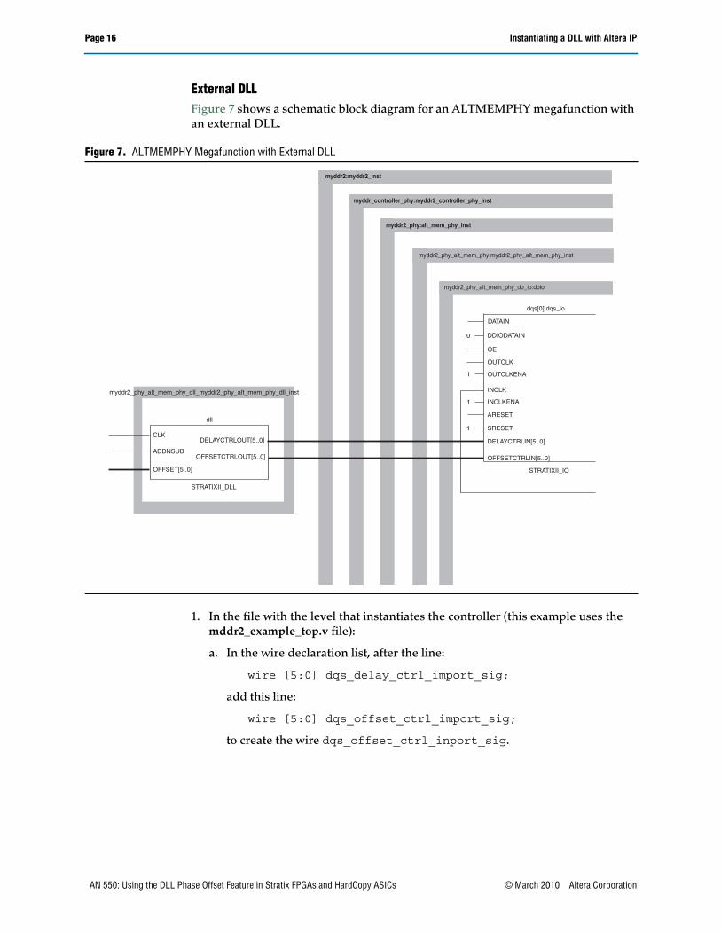
External DLLFigure 7 shows a schematic block diagram for an ALTMEMPHY megafunction withan external DLL.
1. In the file with the level that instantiates the controller (this example uses themddr2_example_top.v file):
a. In the wire declaration list, after the line:
wire [5:0] dqs_delay_ctrl_import_sig;
add this line:
wire [5:0] dqs_offset_ctrl_import_sig;
to create the wire dqs_offset_ctrl_inport_sig.
Figure 7. ALTMEMPHY Megafunction with External DLL
CLK
ADDNSUB
OFFSET[5..0]
DELAYCTRLOUT[5..0]
OFFSETCTRLOUT[5..0]
dll
STRATIXII_DLL
myddr2_phy_alt_mem_phy_dll_myddr2_phy_alt_mem_phy_dll_inst
DATAIN
DDIODATAIN
OE
OUTCLK
OUTCLKENA
INCLK
INCLKENA
ARESET
SRESET
DELAYCTRLIN[5..0]
OFFSETCTRLIN[5..0]
0
1
1
dqs[0].dqs_io
STRATIXII_IO
myddr2:myddr2_inst
myddr_controller_phy:myddr2_controller_phy_inst
myddr2_phy:alt_mem_phy_inst
myddr2_phy_alt_mem_phy:myddr2_phy_alt_mem_phy_inst
myddr2_phy_alt_mem_phy_dp_io:dpio
1
AN 550: Using the DLL Phase Offset Feature in Stratix FPGAs and HardCopy ASICs © March 2010 Altera Corporation

Instantiating a DLL with Altera IP Page 17
b. In the DLL instantiation:
myddr2_phy_alt_mem_phy_dll_sii \myddr2_phy_alt_mem_phy_dll_sii_inst
after the line:
.delayctrlout (dqs_delay_ctrl_import_sig)
add these three ports:
.offsetctrlout (dqs_offset_ctrl_import_sig),
.offset (your_offset_signal),
.addnsub (your_addnsub_signal)
to create the top-level port connections and wires to these ports.
1 For each line you insert, be sure to add a comma to the end of the previousline.
c. Add wire declarations for:
wire [5:0] your_offset_signal
wire your_addnsub_signal
to create the wires that connect your control logic to the DLL.
1 Connect these signals either to pins or registers to control the DLL phaseoffset feature.
d. In the instantiation:
myddr2 myddr2_inst
after the line:
.dqs_delay_ctrl_import (dqs_delay_ctrl_import_sig),
add this line:
.dqs_offset_ctrl_import (dqs_offset_ctrl_import_sig),
to add the top-level port and make the connection fordqs_offset_ctrl_import_sig.
2. In the myddr2_phy_alt_mem_phy_dll_sii.v file:
a. In the port list of the module declaration:
myddr2_phy_alt_mem_phy_dll_sii
add these three ports:
offsetctrlout
offset
addnsub
to create ports to connectoffsetctrlout,offset, andaddnsub to the DLL.
© March 2010 Altera Corporation AN 550: Using the DLL Phase Offset Feature in Stratix FPGAs and HardCopy ASICs

Page 18 Instantiating a DLL with Altera IP
b. In the input and output list, add these three lines:
output [5:0] offsetctrlout;
input [5:0] offset;
input addnsub;
to declare the ports offsetctrlout, offset, and addnsub.
c. In the wire list, add these three lines:
wire [5:0] offsetctrlout;
wire [5:0] offset;
wire addnsub;
to create wires to connect offsetctrlout and offset.
d. In the stratixii_dll dll instantiation, change these three lines:
change:
.addnsub (),
to:
.addnsub(addnsub),
change:
.offset (),
to:
.offset(offset),
and change:
.offsetctrlout (),
to:
.offsetctrlout(offsetctrlout),
to connect addnsub, offset, and offsetctrlout to the DLL.
3. In the filename that you used for your controller (this example uses myddr2), theVerilog file is myddr2.v:
a. In the port list, after:
dqs_delay_ctrl_import,
add this line:
dqs_offset_ctrl_import,
to create a port to connect dqs_offset_ctrl_import.
AN 550: Using the DLL Phase Offset Feature in Stratix FPGAs and HardCopy ASICs © March 2010 Altera Corporation

Instantiating a DLL with Altera IP Page 19
b. In the input declarations, after:
input [5:0] dqs_delay_ctrl_import;
add this line:
input [5:0] dqs_offset_ctrl_import;
to declare the port dqs_offset_ctrl_import.
c. In the instantiation:
myddr2_controller_phy myddr2_controller_phy_inst(
after the line:
.dqs_delay_ctrl_import(dqs_delay_ctrl_import),
add this line:
.dqs_offset_ctrl_import(dqs_offset_ctrl_import),
to create the top-level port and connect the wire todqs_offset_ctrl_import.
4. In the myddr2_controller_phy.v file:
a. In the port list, after:
dqs_delay_ctrl_import,
add this line:
dqs_offset_ctrl_import,
to create port dqs_offset_ctrl_import.
b. In the input declarations, after:
input [5:0] dqs_delay_ctrl_import;
add this line:
input [5:0] dqs_offset_ctrl_import;
to declare port dqs_offset_ctrl_import.
c. In the instantiation:
mddr2_phy alt_mem_phy_inst
after the line:
.dqs_delay_ctrl_import (dqs_delay_ctrl_import),
add this line:
.dqs_offset_ctrl_import (dqs_offset_ctrl_import),
to create the port and make the connection to dqs_offset_ctrl_import.
© March 2010 Altera Corporation AN 550: Using the DLL Phase Offset Feature in Stratix FPGAs and HardCopy ASICs

Page 20 Instantiating a DLL with Altera IP
5. In the myddr2_phy.v file:
a. In the port list, after:
dqs_delay_ctrl_import,
add this line:
dqs_offset_ctrl_import,
to create the port dqs_offset_ctrl_import.
b. In the input declarations, after:
input [5:0] dqs_delay_ctrl_import;
add this line:
input [5:0] dqs_offset_ctrl_import;
to declare the port dqs_offset_ctrl_import.
c. In the instantiation:
mddr2_phy_alt_mem_phy_siimyddr2_phy_alt_mem_phy_sii_inst
after the line:
.dqs_delay_ctrl_import (dqs_delay_ctrl_import),
add this line:
.dqs_offset_ctrl_import (dqs_offset_ctrl_import),
to add the port and make the connection to dqs_offset_ctrl_import.
6. In the myddr2_phy_alt_mem_phy_sii.v file:
a. In the port list of the module:
altmemphy_phy_alt_mem_phy_sii
after the line:
dqs_delay_ctrl_import,
add this line:
dqs_offset_ctrl_import,
to create the port dqs_offset_ctrl_import.
b. In the port declaration list, after the line:
input wire [DQS_DELAY_CTL_WIDTH - 1 : 0 ] \dqs_delay_ctrl_import;
add this line:
input wire [DQS_DELAY_CTL_WIDTH - 1 : 0 ] \dqs_offset_ctrl_import;
to declare the port dqs_offset_ctrl_import.
c. After the wire declaration:
AN 550: Using the DLL Phase Offset Feature in Stratix FPGAs and HardCopy ASICs © March 2010 Altera Corporation

Instantiating a DLL with Altera IP Page 21
wire [DQS_DELAY_CTL_WIDTH - 1 : 0 ] \dqs_delay_ctrl_internal;
add this line:
wire [DQS_DELAY_CTL_WIDTH - 1 : 0 ] \dqs_offset_ctrl_internal;
to declare the wire dqs_offset_ctrl_internal.
d. Before the line:
if (DLL_EXPORT_IMPORT == "IMPORT")
add this line:
assign dqs_offset_ctrl_internal = \dqs_offset_ctrl_import;
to connect dqs_offset_ctrl_import to dqs_offset_ctrl_internal.
e. In the instantiation:
myddr2_phy_alt_mem_phy_dp_io_sii ... dpio(
after the line:
.dqs_delay_ctrl (dqs_delay_ctrl_internal),
add this line:
.dqs_offset_ctrl (dqs_offset_ctrl_internal),
to create the port and make the connection todqs_offset_ctrl_internal.
f. In the module declaration:
module myddr2_phy_alt_mem_phy_dp_io_sii
in the port list, after the line:
dqs_delay_ctrl,
add this line:
dqs_offset_ctrl,
to create the port dqs_offset_ctrl.
g. In the input declaration list, after the line:
input wire [DQS_DELAY_CTL_WIDTH - 1 : 0 ] \dqs_delay_ctrl;
add this line:
input wire [DQS_DELAY_CTL_WIDTH - 1 : 0 ] \dqs_offset_ctrl;
to declare port dqs_offset_ctrl.
© March 2010 Altera Corporation AN 550: Using the DLL Phase Offset Feature in Stratix FPGAs and HardCopy ASICs

Page 22 Instantiating a DLL with Altera IP
h. After the line:
begin : dqs
in the generate block that instantiates dqs stratixii_io, being careful notto change the block that has dq_io, change the line:
.dqs_offsetctrl_enable ("false")
to:
.dqs_offsetctrl_enable ("true")
to enable the DLL phase offset feature in the DQS blocks.
i. In the dqs_io port connection list, change the line:
.offsetctrlin (),
to:
.offsetctrlin (dqs_offset_ctrl),
to connect dqs_offset_ctrl to the offsetctrlin port on the DQS block.
Instantiating the DLL Phase Offset Using the ALTDQS MegafunctionThis section describes how you can instantiate a DLL with Altera IP by using theALTDQS megafunction. You can use this method if you are designing a customDDR PHY interface. When you make the selections in the ALTDQS MegaWizardPlug-In Manager, it makes the connections necessary for the DLL phase offset featureautomatically.
Figure 8 shows page 8 of the ALTDQS MegaWizard Plug-In Manager.
Figure 8. ALTDQS MegaWizard Plug-In Manager (Page 8)
AN 550: Using the DLL Phase Offset Feature in Stratix FPGAs and HardCopy ASICs © March 2010 Altera Corporation

Instantiating a DLL with Altera IP Page 23
On page 8 of the ALTDQS MegaWizard Plug-In Manager, deselect Use static offset…and select Create a ‘dll_addnsub’ port to do both. This creates the addnsub andoffset[5:0]ports. These ports must be brought up to a register (initialized to zero)that is controlled from firmware in your end system.
Making the Connections to Use the DLL Phase Offset Feature with the Legacy Static PHYTo use the DLL phase offset feature with the Legacy Static PHY, you must connect theoffsetctrlout[5:0] output from the DLL to the DQS blocks. The following is ademonstration design to show how to make the connections. In the MegaWizardPlug-In Manager for the Legacy Static PHY, on the controller tab at the bottom, turnon the Insert logic to allow the DLL to update only during the memory refreshperiod option (when turned on, it inserts a register in the delayctrlout path thatcauses it to be out-of-sync with offsetctrlout).
The demonstration design uses:
■ The filename myddr2 in the MegaWizard Plug-In Manager for the name of theLegacy Static PHY.
■ The project name is myddr2_example_top.
■ The top-level module is myddr2_example_top and is contained in the file top.v.
© March 2010 Altera Corporation AN 550: Using the DLL Phase Offset Feature in Stratix FPGAs and HardCopy ASICs

Page 24 Instantiating a DLL with Altera IP
Figure 9 shows a schematic block diagram for a Legacy Static PHY.
To make the connections for using the DLL phase offset feature with the Legacy StaticPHY, perform the following steps:
1. In the top-level file (this example uses myddr2_example_top.v), locate the DLLinstance. In this example, the DLL instance contains the following 10 lines:
myddr2_auk_ddr_dll dll(
.addnsub (1'b0),
.clk (dqs_ref_clk),
.delayctrlout (dqs_delay_ctrl),
.dqsupdate (dqsupdate),
.offset (6'b000000),
.reset_n (soft_reset_reg2_n),
.stratix_dll_control (stratix_dll_control));
Modify the DLL instance to replace the hard coded values 1’b0 and 6’b000000with the signals addnsub and offset, respectively, and add the output portoffsetctrlout.
Figure 9. Legacy Static PHY
CLK
ADDNSUB
OFFSET[5..0]
DELAYCTRLOUT[5..0]
OFFSETCTRLOUT[5..0]
dll
STRATIXII_DLL
myddr2_auk_ddr_dll:dll
capture_clk
clk
control_doing_rd
control_doing_wr
control_dqs_burst
control_wdata_valid
postamble_clk
reset_n
resynch_clk
write_clk
control_be[1..0]
control_wdata[15..0]
dqs_delay_ctr[5..0]
offsetctrlout[5..0]
myddr2_auk_ddr_dqs_group
myddr2:myddr2_ddr_sdram
myddr2_auk_ddr_sdram:myddr2_auk_ddr_sdram_inst
myddr2_auk_ddr_datapath:ddr_io
AN 550: Using the DLL Phase Offset Feature in Stratix FPGAs and HardCopy ASICs © March 2010 Altera Corporation

Instantiating a DLL with Altera IP Page 25
Your new DLL instance has 11 lines and looks like the following:
myddr2_auk_ddr_dll dll(
.addnsub (addnsub), //Changed 1’b0 to addnsub
.clk (dqs_ref_clk),
.delayctrlout (dqs_delay_ctrl),
.offsetctrlout (offsetctrlout), //Added the offsetctrlout port
.dqsupdate (dqsupdate),
.offset (offset), //Changed 6'b000000 to offset
.reset_n (soft_reset_reg2_n),
.stratix_dll_control (stratix_dll_control));
2. In the myddr2_example_top.v file, after:
wire [5:0] dqs_delay_ctrl;
add this line:
wire [5:0] offsetctrlout; //Added offsetctrlout wire.
to declare the wire offsetctrlout.
3. In the myddr2_example_top.v file in the instantiation:
myddr2 myddr2_ddr_sdram
after the line:
.dqs_delay_ctrl (dqs_delay_ctrl),
add this line:
.offsetctrlout (offsetctrlout), //Added offsetctrlout port
to add the port and make the top-level connection for offsetctrlout.
4. In the myddr2_auk_ddr_dll.v file, add the port offsetctrlout to the module:
myddr2_auk_ddr_dll
Also add a wire [5:0] offsetctrlout and connect it to the portoffsetctrlout on the stratixii_dll instantiation.
The Verilog file should look like the following:
module myddr2_auk_ddr_dll (
//inputs:addnsub,clk,offset,reset_n,stratix_dll_control,
//outputs:delayctrlout,offsetctrlout, //Add offsetctrlout portdqsupdate
)
/* synthesis ALTERA_ATTRIBUTE = \"MESSAGE_DISABLE=14130;MESSAGE_DISABLE=14110" */ ;
© March 2010 Altera Corporation AN 550: Using the DLL Phase Offset Feature in Stratix FPGAs and HardCopy ASICs

Page 26 Instantiating a DLL with Altera IP
output [5:0] delayctrlout;output [5:0] offsetctrlout; //Add offsetctrlout portoutput dqsupdate;input addnsub;input clk;input [5:0] offset;input reset_n;input stratix_dll_control;wire [5:0] delayctrlout;wire [5:0] offsetctrlout; //Add offsetctrlout wirewire dqsupdate;
//------------------------------------------------------// Instantiate Stratix II DLL//-------------------------------------------------------
stratixii_dll dll(
.addnsub (addnsub),
.aload (),
.clk (clk),
.delayctrlout (delayctrlout),
.devclrn (),
.devpor (),
.dqsupdate (dqsupdate),
.offset (offset),
.offsetctrlout (offsetctrlout), //Add the offsetctrlout// connection
.upndnin (),
.upndninclkena (),
.upndnout ());
defparam dll.delay_buffer_mode = "low",dll.delay_chain_length = 12,dll.delayctrlout_mode = "normal",dll.input_frequency = "7500ps",dll.jitter_reduction = "false",dll.lpm_type = "stratixii_dll",dll.offsetctrlout_mode = "dynamic_addnsub",
//Make sure this parameter is set to dynamic_addnsubdll.sim_loop_delay_increment = 144,dll.sim_loop_intrinsic_delay = 3600,dll.sim_valid_lock = 1,dll.sim_valid_lockcount = 27,dll.static_delay_ctrl = 0,dll.static_offset = "0",dll.use_upndnin = "false",dll.use_upndninclkena = "false";
The MegaWizard Plug-In Manager sets the above parameters appropriately for thefrequency of your design. The only parameter you typically must change isdll.offsetctrlout_mode to dynamic_addnsub.
Route the offset and addnsub signals up through your design hierarchy to eitherregister configuration pins or directly to jumper-controlled I/Os. Ensure that yoursystem initializes these pins to 0. If you are using I/O control, ensure each of the sevenpins (six for offset and one for addnsub) can be set either to 1 or 0.
1. In the myddr2_auk_ddr_sdram.v file:
a. In the module declaration:
module myddr2_auk_ddr_sdram
AN 550: Using the DLL Phase Offset Feature in Stratix FPGAs and HardCopy ASICs © March 2010 Altera Corporation

Instantiating a DLL with Altera IP Page 27
after the port: dqs_delay_ctrl,
add the port:
offsetctrlout,
in the input declaration section, add:
input [5:0] offsetctrlout; //Add offsetctrlout port
b. In the module instantiation:
myddr2_auk_ddr_datapath ddr_io
after the port connection: .dqs_delay_ctrl (dqs_delay_ctrl),
add this line:
.offsetctrlout(offsetctrlout), //Add offsetctrlout port
to add the port and make the connection for offsetctrlout.
2. In the myddr2.v file:
a. In the module declaration:
module myddr2
after the port: dqs_delay_ctrl,
add the port:
offsetctrlout,
in the input declaration section, add:
input [5:0] offsetctrlout; //Add offsetctrlout port
b. In the module instantiation:
myddr2_auk_ddr_sdram myddr2_auk_ddr_sdram_inst
after the port connection: .dqs_delay_ctrl (dqs_delay_ctrl),
add this line:
.offsetctrlout(offsetctrlout), //Add offsetctrlout port
to add the port and make the connection for offsetctrlout.
3. In the myddr2_auk_ddr_datapath.v file:
a. In the module declaration:
module myddr2_auk_ddr_datapath
after the port: dqs_delay_ctrl,
add the port:
offsetctrlout,
in the input declaration section, add:
input [5:0] offsetctrlout; //Added offsetctrlout port
© March 2010 Altera Corporation AN 550: Using the DLL Phase Offset Feature in Stratix FPGAs and HardCopy ASICs

Page 28 Instantiating a DLL with Altera IP
b. In the module instantiation:
myddr2_auk_ddr_dqs_group \g_datapath:N:g_ddr_io
where the “N” goes from 0 to the width of the DDR DQS bus minus 1, after theport connection: .dqs_delay_ctrl (dqs_delay_ctrl),
add this line:
.offsetctrlout(offsetctrlout), //Add offsetctrlout port
4. In the myddr2_auk_ddr_dqs_group.v file:
a. In the module declaration:
module myddr2_auk_ddr_dqs_group
after the port: dqs_delay_ctrl,
add the port:
offsetctrlout,
in the input declaration section, add:
input [5:0] offsetctrlout; //Added offsetctrlout port
b. In the module instantiation:
stratixii_io dqs_io
after the port: .delayctrlin(dqs_delay_ctrl),
add the port:
.offsetctrlin(offstectrlout),
Do this in both the SIMULATION-ONLY CONTENTS and the //synthesistranslate_on sections.
In both the “simulation” and “synthesis defparam” sections of theinstantiation, change the parameter:
dqs_io.dqs_offsetstrl_enable = "false"
to:
dqs_io.dqs_offsetstrl_enable = "true"
1 Take care to change ONLY DQS instantiations; do NOT change the DQ I/Oinstantiations g_dq_io:?:dq_io .offsetctrl_enable, as these arefor the DQ pins, not the DQS pins.
AN 550: Using the DLL Phase Offset Feature in Stratix FPGAs and HardCopy ASICs © March 2010 Altera Corporation
Confirm Your DLL Phase Offset Control Settings Page 29
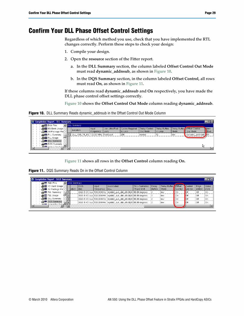
Confirm Your DLL Phase Offset Control SettingsRegardless of which method you use, check that you have implemented the RTLchanges correctly. Perform these steps to check your design:
1. Compile your design.
2. Open the resource section of the Fitter report.
a. In the DLL Summary section, the column labeled Offset Control Out Modemust read dynamic_addnsub, as shown in Figure 10.
b. In the DQS Summary section, in the column labeled Offset Control, all rowsmust read On, as shown in Figure 11.
If these columns read dynamic_addnsub and On respectively, you have made theDLL phase control offset settings correctly.
Figure 10 shows the Offset Control Out Mode column reading dynamic_addnsub.
Figure 11 shows all rows in the Offset Control column reading On.
Figure 10. DLL Summary Reads dynamic_addnsub in the Offset Control Out Mode Column
Figure 11. DQS Summary Reads On in the Offset Control Column
© March 2010 Altera Corporation AN 550: Using the DLL Phase Offset Feature in Stratix FPGAs and HardCopy ASICs

Page 30 Document Revision History
101 Innovation DriveSan Jose, CA 95134www.altera.comTechnical Supportwww.altera.com/support
Copyright © 2010 Altera Corporation. All rights reserved. Altera, The Programmable Solutions Company, the stylizedAltera logo, specific device designations, and all other words and logos that are identified as trademarks and/or servicemarks are, unless noted otherwise, the trademarks and service marks of Altera Corporation in the U.S. and othercountries. All other product or service names are the property of their respective holders. Altera products are protectedunder numerous U.S. and foreign patents and pending applications, maskwork rights, and copyrights. Altera warrantsperformance of its semiconductor products to current specifications in accordance with Altera's standard warranty,but reserves the right to make changes to any products and services at any time without notice. Altera assumes noresponsibility or liability arising out of the application or use of any information, product, or servicedescribed herein except as expressly agreed to in writing by Altera Corporation. Altera customers areadvised to obtain the latest version of device specifications before relying on any publishedinformation and before placing orders for products or services.
Document Revision HistoryTable 3 shows the revision history for this application note.
Table 3. Document Revision History
Date Version Changes Made
March 2010 2.0 ■ Changed “HardCopy II” and “HardCopy devices” to “HardCopy ASICs” when referringto the HardCopy device family.
■ Changed “Stratix II” and “Stratix devices” to “Stratix FPGAs” when referring to theStratix device family.
■ Updated Table 1 and Table 2.
■ Updated Figure 4 and Figure 5 with color.
■ Minor text edits.
November 2008 1.0 Initial Release.