an-2149lm5113 evaluation board - texas · pdf file · 2013-05-06snva484a–...
TRANSCRIPT

User's GuideSNVA484A–October 2011–Revised May 2013
AN-2149 LM5113 Evaluation Board
1 Introduction
The LM5113 evaluation board is designed to provide the design engineers with a synchronous buckconverter to evaluate the LM5113, a 100V half-bridge enhancement mode Gallium Nitride (GaN) FETdriver. The active clamping voltage mode controller LM5025 is used to generate the PWM signals of thebuck switch and the synchronous switch. The specifications of the evaluation board are as follows:
• Input Operating Voltage: 15V to 60V
• Output Voltage: 10V
• Output Current: 10A @ 48V, 7A @ 60V
• Measured Efficiency at 48V: 93.9% @ 10A
• Frequency of Operation: 800kHz
• Line UVLO: 13.8V (Rising) /10.8V (Falling)
• Board size: 3.00 x 2.83 inches
The printed circuit board (PCB) consists of 2 layers of 2 ounce copper on FR4 material, with a thickness of0.050 inches.
This document contains the schematic of the evaluation board, Bill of Materials (BOM) and a quick setupprocedure. The evaluation board can be reconfigured for different switching frequency, dead time, and theoutput voltage from the specifications above. An example of 48V to 3.3V conversion is given inAppendix A. For more complete information, see the LM5113 5A, 100V Half-Bridge Gate Driver forEnhancement Mode GaN FETs Data Sheet (SNVS725)
2 IC Features• Independent high-side and low-side TTL logic inputs
• 1.2A/5A peak source/sink current
• High-side floating bias voltage rail operates up to 100VDC
• Internal bootstrap supply voltage clamping
• Split outputs for adjustable turn-on/turn-off strength
• 0.6Ω/2.1Ω pull-down/pull-up resistance
• Fast propagation times (28 ns typical)
• Excellent propagation delay matching (1.5 ns typical)
• Supply rail under-voltage lockout
• Low power consumption
3 Powering and Loading Considerations
Certain precautions need to be followed when applying power to the LM5113 evaluation board. Amisconnection can damage the assembly.
All trademarks are the property of their respective owners.
1SNVA484A–October 2011–Revised May 2013 AN-2149 LM5113 Evaluation BoardSubmit Documentation Feedback
Copyright © 2011–2013, Texas Instruments Incorporated

DC Power Supply
J1 VIN
GNDJ3
J2J4
VOUT
LM5113 EVAL
Current Meter
Volt-meter
GND
+
-
+ Electronic Loadwith current meter-
LOH
UVLO
HOHLEVELSHIFT
HB
HS
VDD
VSS
HI
LI
HOL
LOL
UVLO & CLAMP
Powering and Loading Considerations www.ti.com
3.1 Proper Board Connection
Figure 2 depicts the typical evaluation setup. The source power is connected to the J1 (VIN) and the J3(GND). The load is connected to the J2 (VOUT) and the J4 (GND). Be sure to choose the correctconnector and wire size. The input and output voltage must be monitored directly at the terminals of theboard. The voltage drop across the connection wires will cause inaccurate measurements.
Figure 1. Simplified Block Diagram of LM5113
Figure 2. Typical Evaluation Setup
3.2 Source Power
To fully test the LM5113 evaluation board, a DC power supply capable of 60V and 8A is required. Thepower supply and cabling must present low impedance to the evaluation board. Insufficient cabling or ahigh impedance power supply will droop during power supply application with the evaluation board inrushcurrent. If large enough, this droop will cause a chattering condition upon power up. This chatteringcondition is an interaction with the evaluation board under voltage lockout, the cabling impedance and theinrush current.
2 AN-2149 LM5113 Evaluation Board SNVA484A–October 2011–Revised May 2013Submit Documentation Feedback
Copyright © 2011–2013, Texas Instruments Incorporated

15 20 25 30 35 40 45 50 55 60
6
7
8
9
10
11
12
LOA
D C
UR
RE
NT
(A
)
VIN (V)
@Room temperaturewith airflow of 200CFM
www.ti.com Powering and Loading Considerations
3.3 Output Current Derating
The LM5113 evaluation board is designed to operate with a maximum load current of 10A for inputvoltages ranging from 15V to 48V. With further increases of the input voltage, the maximum allowable loadcurrent gradually decreases to 7A, to ensure reliable prolonged operation. Figure 3 illustrates the deratingcurve of the output current at room temperature with airflow of 200CFM. It may be necessary to furtherreduce the maximum load current at higher ambient temperature.
Note that the LM5113 evaluation board does not have over current protection. Certain precautions shouldbe taken to prevent the load current from exceeding the derating curve shown in Figure 3, otherwise acatastrophic failure may result.
3.4 Air Flow
Sufficient cooling is required to ensure a proper and reliable operation. Especially at high line input and fullload, most of the power losses are dissipated in the buck switch. Insufficient airflow can cause overheatingof the GaN FETs. A minimum airflow of 200CFM should always be provided.
3.5 Quick Start-Up Procedure1. Set the current limit of the source supply to provide about 1.5 times the anticipated output power.
Connect the source supply to J1 and J3.
2. Connect the load cable between J2 and J4. Disable the load.
3. Set the input voltage and turn on the power supply without load current. Check that the output voltageis 10V.
4. Slowly increase the load current while monitoring the output voltage.
When the evaluation board is powered off, wait for 30 seconds before powering on the evaluation boardagain to allow the full discharge of the soft start capacitor.
Figure 3. Load Current Derating Curve
3SNVA484A–October 2011–Revised May 2013 AN-2149 LM5113 Evaluation BoardSubmit Documentation Feedback
Copyright © 2011–2013, Texas Instruments Incorporated

1 2 3 4 5 6 7 8 9 10
82
84
86
88
90
92
94
96
98
100
EF
FIC
IEN
CY
(%
)
LOAD CURRENT (A)
15V 24V 36V 48V
60V
fSW=800kHz
VOUT=10V
Performance Characteristics www.ti.com
4 Performance Characteristics
Figure 4 shows the efficiency of the LM5113 evaluation board at different input voltage and the loadcurrent. 30ns dead time between HI and LI input of the LM5113 is selected to eliminate the shoot throughwhile achieving high efficiency.
Figure 4. Evaluation Board Efficiency vs. Load Current
During the dead time, the HS pin voltage can be pulled down below -0.7V and results in an excessivebootstrap voltage. The LM5113 has an internal clamping circuitry that prevents the bootstrap voltage fromexceeding 5.25V typically. Figure 5 shows the average of the bootstrap voltage with the different loadcurrent. As can be seen, the bootstrap voltage is well regulated.
Figure 5. Bootstrap Voltage Regulation vs. Load Current
4 AN-2149 LM5113 Evaluation Board SNVA484A–October 2011–Revised May 2013Submit Documentation Feedback
Copyright © 2011–2013, Texas Instruments Incorporated

www.ti.com Performance Characteristics
Figure 6 compares the input and the output of the low-side driver.
Conditions:Input Voltage = 48V DC, Load Current = 5ATraces:Top Trace: Gate of Low-Side eGaN FET, Volt/div = 2VBottom Trace: LI of LM5113, Volt/div = 5VBandwidth Limit = 600MHzHorizontal Resolution = 0.2 µs/div
Figure 6. Low-Side Driver Input and Output
Figure 7 shows the switch node voltage that is also the drain voltage of the low-side FET. The ringing onthe switch node voltage can be reduced by the HOH gate resistor. 2Ω HOH gate resistance is selected toachieve a drain-source voltage margin of 12V for a 60V input.
Conditions:Input Voltage = 48V DCLoad Current = 10ATraces:Trace: Switch–Node Voltage, Volts/div = 20VBandwidth Limit = 600 MHzHorizontal Resolution = 50 ns/div
Figure 7. Switch-Node Voltage
5SNVA484A–October 2011–Revised May 2013 AN-2149 LM5113 Evaluation BoardSubmit Documentation Feedback
Copyright © 2011–2013, Texas Instruments Incorporated
Performance Characteristics www.ti.com
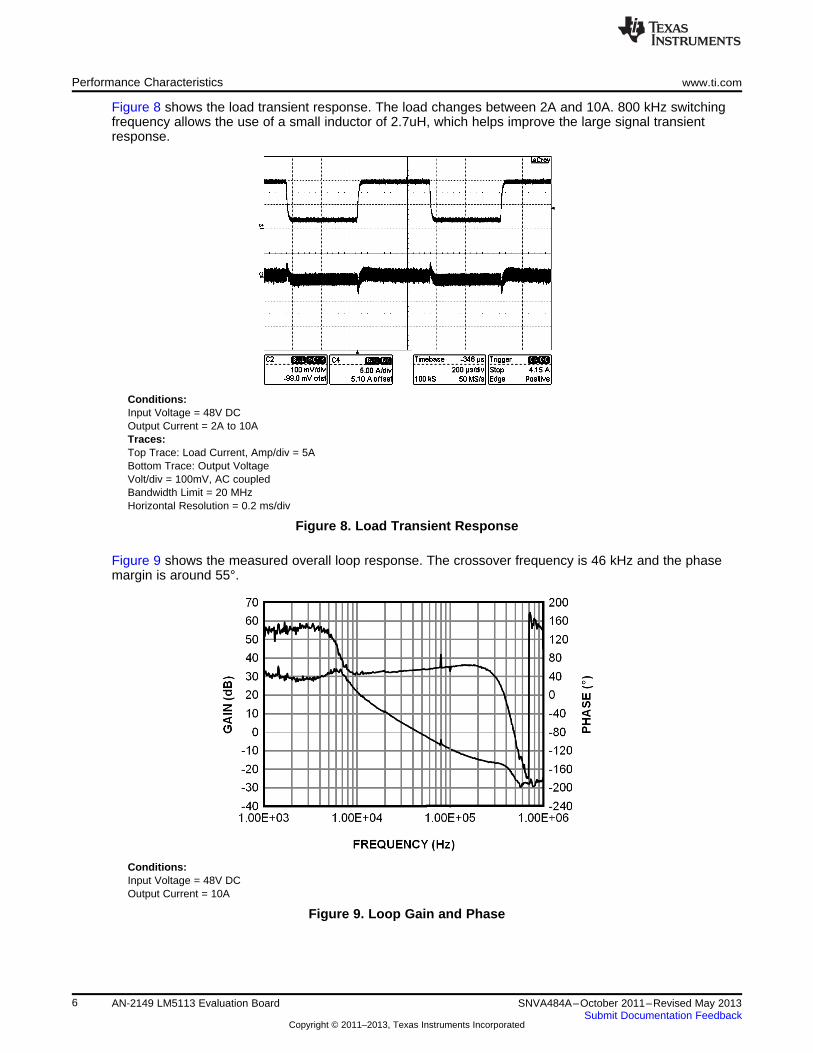
Figure 8 shows the load transient response. The load changes between 2A and 10A. 800 kHz switchingfrequency allows the use of a small inductor of 2.7uH, which helps improve the large signal transientresponse.
Conditions:Input Voltage = 48V DCOutput Current = 2A to 10ATraces:Top Trace: Load Current, Amp/div = 5ABottom Trace: Output VoltageVolt/div = 100mV, AC coupledBandwidth Limit = 20 MHzHorizontal Resolution = 0.2 ms/div
Figure 8. Load Transient Response
Figure 9 shows the measured overall loop response. The crossover frequency is 46 kHz and the phasemargin is around 55°.
Conditions:Input Voltage = 48V DCOutput Current = 10A
Figure 9. Loop Gain and Phase
6 AN-2149 LM5113 Evaluation Board SNVA484A–October 2011–Revised May 2013Submit Documentation Feedback
Copyright © 2011–2013, Texas Instruments Incorporated

2.2
F2.
2
F2.
2
F2.
2
F2.
2
F2.
2
FV
IN J3
C2
C3
C4
C5
C6
C7
VIN
J1
TP
4
+
+-
GN
D
GN
DG
ND
GN
D
GN
D
GN
D
OU
TIN O
N/O
FF
BY
PC
180.
1
FC
191
F
R7
33.2
kC
17N
U
R4
±1%
49
.9
U1
LP
2982
AIM
5-5.
05V
5 4
C20
100
pFC
212.
2
F
2
C24
1
F6.
3V
C25
0.1
F
GN
D
D3
NU
R11 0R
D4
GN
D
U3 HB
HS
VD
DH
OH
HI
HO
L
LOH
LOL
VS
S
LI
25 3 4 10 9
8761
EP
LM51
13
GN
D
NU
R14
0RC
27N
UC
28N
U
R15
4.02
k
¬¬¬¬
¬ ¬
¬ ¬ ¬
¬
R18
CO
MP
SY
NC
RT
TIM
ER
EF
VC
CA
GN
DP
GN
D
OU
TB
SS
RA
MP
OU
TA
UV
LOC
S2
CS
1V
IN
U4
16
1 2 12 15 14 6
3 4 8 9 13 5 11 107
LM50
25C
300.
01
FC
310.
1
F
R17
7.50
kC
321
F
GN
D
GN
D
0
D5
D6
MB
R13
0T1G
1N41
48W
-7-F
R19
21.0
k
GN
D
GN
D
R16
21.0
k
C29
1
F
GN
D
U2
LM82
61M
5C
261
F
C23
1500
pF
C22
330
pF
R8
16.9
k
2
41
5
3
R5
374
C15
1.5
nF
R6
21.0
k
R1
10.0
C1
330
FC
1222
F
C10
22
FC
111
FC
141
uF
C13
NU
SE
R13
60-2
72K
L2.
7
H
L1
1
23579
11
468
10
Q
2E
PC
2001
D2
MB
R13
0T1G
GN
D
GN
D
GN
D
J4
VO
UT
10V
J2V
OU
TT
P2
TP
5
1110
9 7 5 3
8 6 4 2 Q1
EP
C20
01
1
C9
0.01
uF
C8
0.1
uF
TP
3
TP
1E
X V
CC
GN
D
D1
MB
R13
0T1G
R2
100k
±1%
R3
150k
C16
220
pF
R13
6.98
k
R9
2RR
100R
¬
1 3
www.ti.com Evaluation Board Schematic
5 Evaluation Board Schematic
Figure 10. Application Circuit: Input 15V to 60V, Output 10V, 800 kHz
7SNVA484A–October 2011–Revised May 2013 AN-2149 LM5113 Evaluation BoardSubmit Documentation Feedback
Copyright © 2011–2013, Texas Instruments Incorporated
Bill of Materials (BOM) www.ti.com
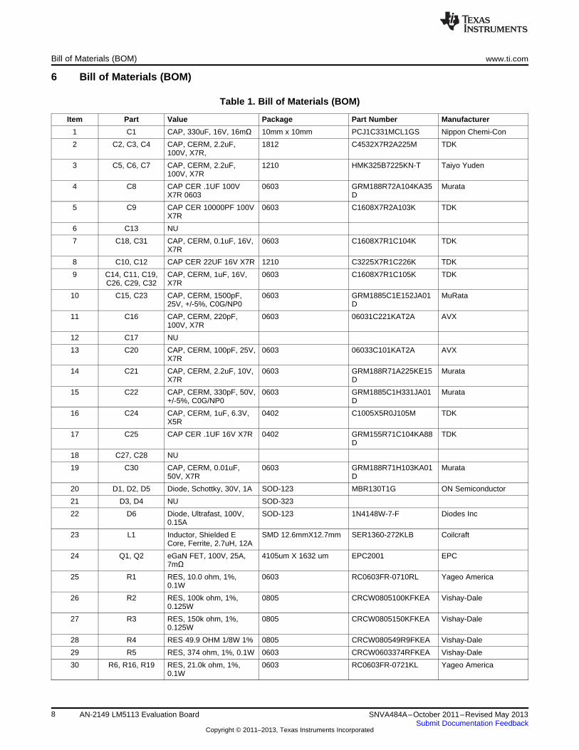
6 Bill of Materials (BOM)
Table 1. Bill of Materials (BOM)
Item Part Value Package Part Number Manufacturer
1 C1 CAP, 330uF, 16V, 16mΩ 10mm x 10mm PCJ1C331MCL1GS Nippon Chemi-Con
2 C2, C3, C4 CAP, CERM, 2.2uF, 1812 C4532X7R2A225M TDK100V, X7R,
3 C5, C6, C7 CAP, CERM, 2.2uF, 1210 HMK325B7225KN-T Taiyo Yuden100V, X7R
4 C8 CAP CER .1UF 100V 0603 GRM188R72A104KA35 MurataX7R 0603 D
5 C9 CAP CER 10000PF 100V 0603 C1608X7R2A103K TDKX7R
6 C13 NU
7 C18, C31 CAP, CERM, 0.1uF, 16V, 0603 C1608X7R1C104K TDKX7R
8 C10, C12 CAP CER 22UF 16V X7R 1210 C3225X7R1C226K TDK
9 C14, C11, C19, CAP, CERM, 1uF, 16V, 0603 C1608X7R1C105K TDKC26, C29, C32 X7R
10 C15, C23 CAP, CERM, 1500pF, 0603 GRM1885C1E152JA01 MuRata25V, +/-5%, C0G/NP0 D
11 C16 CAP, CERM, 220pF, 0603 06031C221KAT2A AVX100V, X7R
12 C17 NU
13 C20 CAP, CERM, 100pF, 25V, 0603 06033C101KAT2A AVXX7R
14 C21 CAP, CERM, 2.2uF, 10V, 0603 GRM188R71A225KE15 MurataX7R D
15 C22 CAP, CERM, 330pF, 50V, 0603 GRM1885C1H331JA01 Murata+/-5%, C0G/NP0 D
16 C24 CAP, CERM, 1uF, 6.3V, 0402 C1005X5R0J105M TDKX5R
17 C25 CAP CER .1UF 16V X7R 0402 GRM155R71C104KA88 TDKD
18 C27, C28 NU
19 C30 CAP, CERM, 0.01uF, 0603 GRM188R71H103KA01 Murata50V, X7R D
20 D1, D2, D5 Diode, Schottky, 30V, 1A SOD-123 MBR130T1G ON Semiconductor
21 D3, D4 NU SOD-323
22 D6 Diode, Ultrafast, 100V, SOD-123 1N4148W-7-F Diodes Inc0.15A
23 L1 Inductor, Shielded E SMD 12.6mmX12.7mm SER1360-272KLB CoilcraftCore, Ferrite, 2.7uH, 12A
24 Q1, Q2 eGaN FET, 100V, 25A, 4105um X 1632 um EPC2001 EPC7mΩ
25 R1 RES, 10.0 ohm, 1%, 0603 RC0603FR-0710RL Yageo America0.1W
26 R2 RES, 100k ohm, 1%, 0805 CRCW0805100KFKEA Vishay-Dale0.125W
27 R3 RES, 150k ohm, 1%, 0805 CRCW0805150KFKEA Vishay-Dale0.125W
28 R4 RES 49.9 OHM 1/8W 1% 0805 CRCW080549R9FKEA Vishay-Dale
29 R5 RES, 374 ohm, 1%, 0.1W 0603 CRCW0603374RFKEA Vishay-Dale
30 R6, R16, R19 RES, 21.0k ohm, 1%, 0603 RC0603FR-0721KL Yageo America0.1W
8 AN-2149 LM5113 Evaluation Board SNVA484A–October 2011–Revised May 2013Submit Documentation Feedback
Copyright © 2011–2013, Texas Instruments Incorporated

www.ti.com PCB Layouts
Table 1. Bill of Materials (BOM) (continued)
Item Part Value Package Part Number Manufacturer
31 R7 RES, 33.2k ohm, 1%, 0603 RC0603FR-0733K2L Yageo America0.1W
32 R8 RES, 16.9k ohm, 1%, 0603 RC0603FR-0716K9L Yageo America0.1W
33 R9 RES, 2.00 ohm, 1%, 0402 CRCW04022R00FKED Vishay-Dale0.063W
34 R10 RES, 0.0 Ohm, 1/10W 0402 ERJ-2GE0R00X Panasonic
35 R11, R14, R18 RES, 0 ohm, 5%, 0.1W 0603 ERJ-3GEY0R00V Panasonic
36 R13 RES, 6.98k ohm, 1%, 0603 RC0603FR-076K98L Yageo America0.1W
37 R15 RES, 4.02k ohm, 1%, 0603 RC0603FR-074K02L Yageo America0.1W
38 R17 RES, 7.50k ohm, 1%, 0603 CRCW06037K50FKEA Vishay-Dale0.1W
39 U1 5.0V, 50 mA LDO SOT-23 LP2982 Texas Instruments
40 U2 Op Amp SOT-23 LM8261 Texas Instruments
41 U3 5A, 100V, GaN FET DSBGA-10 LM5113 Texas InstrumentsDriver
42 U4 Active clamp voltage 16–pin TSSOP LM5025 Texas Instrumentsmode PWM Controller
7 PCB Layouts
Figure 11. Top Side Silk Screen
9SNVA484A–October 2011–Revised May 2013 AN-2149 LM5113 Evaluation BoardSubmit Documentation Feedback
Copyright © 2011–2013, Texas Instruments Incorporated

PCB Layouts www.ti.com
Figure 12. Bottom Side Silk Screen
Figure 13. Top Layer
10 AN-2149 LM5113 Evaluation Board SNVA484A–October 2011–Revised May 2013Submit Documentation Feedback
Copyright © 2011–2013, Texas Instruments Incorporated

www.ti.com PCB Layouts
Figure 14. Bottom Layer
11SNVA484A–October 2011–Revised May 2013 AN-2149 LM5113 Evaluation BoardSubmit Documentation Feedback
Copyright © 2011–2013, Texas Instruments Incorporated

0
0
21 VR16 k
20 V
u :
www.ti.com
Appendix A 48V to 3.3V Conversion
The LM5113 evaluation board can also be reconfigured for different switching frequency, dead time andoutput voltage. By adjusting the resistor R17, the PWM controller LM5025 can operate up to 1MHz. Thedead time can be adjusted with the resistor R15, and/or with RCD circuitry at the inputs of the LM5113.The output voltage can be adjusted with R16 as follows:
(1)
It should be noted that the maximum output power may be derated to ensure the safe operation of theGaN FETs when the evaluation board is configured for the switching frequency beyond the precedingspecifications.
Figure 15 shows the design for a 48V to 3.3V conversion. The switching frequency is set at 500 kHz. Itshould be noted that the bias supply for the control circuitry is generated from the internal LDO of theLM5025. To aid thermal dissipation, sufficient cooling should be provided for the LM5025. Alternatively, anexternal 10V supply can be connected to the terminal TP1 EXT VCC to provide the bias voltage for thecontrol circuitry.
12 48V to 3.3V Conversion SNVA484A–October 2011–Revised May 2013Submit Documentation Feedback
Copyright © 2011–2013, Texas Instruments Incorporated

2.2
F2.
2
F2.
2
F2.
2
F2.
2
F2.
2
F
VIN
48V
J3
C2
C3
C4
C5
C6
C7
VIN
J1
TP
4
+
+-
GN
D
GN
DG
ND
GN
D
GN
D
GN
D
OU
TIN O
N/O
FF
BY
PC
180.
1
FC
191
F
R7
33.2
kC
17N
U
R4
±1%
49
.9
U1
LP
2982
AIM
5-5.
05V
5 4
C20
100
pFC
212.
2
F
2
C24
1
F6.
3V
C25
0.1
F
GN
D
D3
NU
R11 0R
D4
GN
D
U3 HB
HS
VD
DH
OH
HI
HO
L
LOH
LOL
VS
S
LI
25 3 4 1 0 9
8761
EP
LM51
13
GN
D
NU
R14
0RC
27N
UC
28N
U
R15
4.02
k
¬¬¬¬
¬ ¬
¬ ¬ ¬
¬
R18
CO
MP
SY
NC
RT
TIM
ER
EF
VC
CA
GN
DP
GN
D
OU
TB
SS
RA
MP
OU
TA
UV
LOC
S2
CS
1V
IN
U4
16
1 2 12 15 14 6
3 4 8 9 13 5 11 107 LM
5025
MT
CE
/NO
PB
LM50
25 M
TC
EC
T-N
DC
300.
01
FC
310.
1
F
R17
12k
C32
1
F
GN
D
GN
D
0
D5
D6
MB
R13
0T1G
1N41
48W
-7-F
R19
21.0
k
GN
D
GN
D
R16
4.1k
C29
1
F
GN
D
U2
LM82
61M
5C
261
F
C23
4.7
nF
C22
220
pF
R8
7.8k
2
41
5
3
R5
374
C15
1.5
nF
R6
21k
R1
10.0
C1
330
FC
1222
F
C10
22
FC
111
FC
141
uF
C13
NU
SE
R13
60-2
72K
L2.
7
H
L1
1
23579
11
468
10
Q
2E
PC
2001
D2
MB
R13
0T1G
GN
D
GN
D
GN
D
J4
VO
UT
3.3VJ2
VO
UT
TP
2
TP
5
1110
9 7 5 3
8 6 4 2 Q1
EP
C20
01
1
C9
0.01
uF
C8
0.1
uF
TP
3
TP
1E
X V
CC
GN
D
D1
MB
R13
0T1G
R2
100k
±1%
R3
150k
C16
220
pF
R13
6.98
k
R9
2RR
100R
¬
1 3
www.ti.com Appendix A
Figure 15. Application Circuit: Input 48V, Output 3.3V, 10A, 500 kHz
13SNVA484A–October 2011–Revised May 2013 48V to 3.3V ConversionSubmit Documentation Feedback
Copyright © 2011–2013, Texas Instruments Incorporated

IMPORTANT NOTICE
Texas Instruments Incorporated and its subsidiaries (TI) reserve the right to make corrections, enhancements, improvements and otherchanges to its semiconductor products and services per JESD46, latest issue, and to discontinue any product or service per JESD48, latestissue. Buyers should obtain the latest relevant information before placing orders and should verify that such information is current andcomplete. All semiconductor products (also referred to herein as “components”) are sold subject to TI’s terms and conditions of salesupplied at the time of order acknowledgment.
TI warrants performance of its components to the specifications applicable at the time of sale, in accordance with the warranty in TI’s termsand conditions of sale of semiconductor products. Testing and other quality control techniques are used to the extent TI deems necessaryto support this warranty. Except where mandated by applicable law, testing of all parameters of each component is not necessarilyperformed.
TI assumes no liability for applications assistance or the design of Buyers’ products. Buyers are responsible for their products andapplications using TI components. To minimize the risks associated with Buyers’ products and applications, Buyers should provideadequate design and operating safeguards.
TI does not warrant or represent that any license, either express or implied, is granted under any patent right, copyright, mask work right, orother intellectual property right relating to any combination, machine, or process in which TI components or services are used. Informationpublished by TI regarding third-party products or services does not constitute a license to use such products or services or a warranty orendorsement thereof. Use of such information may require a license from a third party under the patents or other intellectual property of thethird party, or a license from TI under the patents or other intellectual property of TI.
Reproduction of significant portions of TI information in TI data books or data sheets is permissible only if reproduction is without alterationand is accompanied by all associated warranties, conditions, limitations, and notices. TI is not responsible or liable for such altereddocumentation. Information of third parties may be subject to additional restrictions.
Resale of TI components or services with statements different from or beyond the parameters stated by TI for that component or servicevoids all express and any implied warranties for the associated TI component or service and is an unfair and deceptive business practice.TI is not responsible or liable for any such statements.
Buyer acknowledges and agrees that it is solely responsible for compliance with all legal, regulatory and safety-related requirementsconcerning its products, and any use of TI components in its applications, notwithstanding any applications-related information or supportthat may be provided by TI. Buyer represents and agrees that it has all the necessary expertise to create and implement safeguards whichanticipate dangerous consequences of failures, monitor failures and their consequences, lessen the likelihood of failures that might causeharm and take appropriate remedial actions. Buyer will fully indemnify TI and its representatives against any damages arising out of the useof any TI components in safety-critical applications.
In some cases, TI components may be promoted specifically to facilitate safety-related applications. With such components, TI’s goal is tohelp enable customers to design and create their own end-product solutions that meet applicable functional safety standards andrequirements. Nonetheless, such components are subject to these terms.
No TI components are authorized for use in FDA Class III (or similar life-critical medical equipment) unless authorized officers of the partieshave executed a special agreement specifically governing such use.
Only those TI components which TI has specifically designated as military grade or “enhanced plastic” are designed and intended for use inmilitary/aerospace applications or environments. Buyer acknowledges and agrees that any military or aerospace use of TI componentswhich have not been so designated is solely at the Buyer's risk, and that Buyer is solely responsible for compliance with all legal andregulatory requirements in connection with such use.
TI has specifically designated certain components as meeting ISO/TS16949 requirements, mainly for automotive use. In any case of use ofnon-designated products, TI will not be responsible for any failure to meet ISO/TS16949.
Products Applications
Audio www.ti.com/audio Automotive and Transportation www.ti.com/automotive
Amplifiers amplifier.ti.com Communications and Telecom www.ti.com/communications
Data Converters dataconverter.ti.com Computers and Peripherals www.ti.com/computers
DLP® Products www.dlp.com Consumer Electronics www.ti.com/consumer-apps
DSP dsp.ti.com Energy and Lighting www.ti.com/energy
Clocks and Timers www.ti.com/clocks Industrial www.ti.com/industrial
Interface interface.ti.com Medical www.ti.com/medical
Logic logic.ti.com Security www.ti.com/security
Power Mgmt power.ti.com Space, Avionics and Defense www.ti.com/space-avionics-defense
Microcontrollers microcontroller.ti.com Video and Imaging www.ti.com/video
RFID www.ti-rfid.com
OMAP Applications Processors www.ti.com/omap TI E2E Community e2e.ti.com
Wireless Connectivity www.ti.com/wirelessconnectivity
Mailing Address: Texas Instruments, Post Office Box 655303, Dallas, Texas 75265Copyright © 2013, Texas Instruments Incorporated