an-1779lm2756 multi-displayinductorless led driver with 32
TRANSCRIPT

Application ReportSNVA318A–March 2008–Revised April 2013
AN-1779 LM2756 Multi-Display Inductorless LED Driverwith 32 Exponential Dimming Steps in µSMD
.....................................................................................................................................................
ABSTRACT
This application note discusses the ways in which the LM2756 can be configured to drive the eight LEDsin numerous configurations.
Contents1 Typical Application .......................................................................................................... 32 Basic Description ............................................................................................................ 33 Bill of Materials .............................................................................................................. 34 LM2756 Evaluation Board Schematic .................................................................................... 45 LM2756 Evaluation Board Layout ........................................................................................ 46 Board Operation ............................................................................................................. 6
6.1 Basic Connections ................................................................................................. 66.2 External Control Interface Connection .......................................................................... 66.3 Operation Description ............................................................................................. 6
7 Software Interface Information ........................................................................................... 11
List of Figures
1 Top Layer .................................................................................................................... 4
2 Middle Layer 1............................................................................................................... 5
3 Middle Layer 2............................................................................................................... 5
4 Bottom Layer (unmirrored)................................................................................................. 5
5 Data Validity Diagram ...................................................................................................... 6
6 Start and Stop Conditions.................................................................................................. 7
7 Write Cycle .................................................................................................................. 7
8 Chip Address ................................................................................................................ 7
9 General Purpose Register Description Internal Hex Address: 10h................................................... 8
10 Brightness Control Register Description Internal Hex Address: 0xA0 (GroupA), 0xB0 (GroupB), 0xC0(GroupC) ..................................................................................................................... 8
11 Ramp Step Time Register Description Internal Hex Address: 20h ................................................. 10
12 VF Monitor Delay Register Description Internal Hex Address: 60h................................................. 10
13 GUI Start-Up ............................................................................................................... 11
14 Generic Read/Write Field................................................................................................. 12
15 Drop Down Menu .......................................................................................................... 12
16 Control and Configuration Buttons ...................................................................................... 12
17 Brightness Control Sliders................................................................................................ 12
18 BankA Ramp Step Time .................................................................................................. 13
19 Results of Pressing the Set Button...................................................................................... 13
20 Example Configuration.................................................................................................... 13
List of Tables
1SNVA318A–March 2008–Revised April 2013 AN-1779 LM2756 Multi-Display Inductorless LED Driver with 32 ExponentialDimming Steps in µSMDSubmit Documentation Feedback
Copyright © 2008–2013, Texas Instruments Incorporated

www.ti.com
1 Brightness Level Control Table (GroupA) ............................................................................... 9
2 Brightness Ramp-Up/Ramp-Down Times .............................................................................. 11
2 AN-1779 LM2756 Multi-Display Inductorless LED Driver with 32 Exponential SNVA318A–March 2008–Revised April 2013Dimming Steps in µSMD Submit Documentation Feedback
Copyright © 2008–2013, Texas Instruments Incorporated
LM2756
D1A
VIN VOUT
-+
D2A D3A D4A D53
I2C Control Signals
D1B
SDIO
1 µF1 µF1 µF
1 µF GND
D62
C1+
C1-
C2+
C2- SCL
D1C
HWEN
GROUP A
GROUP B GROUP C
ISET
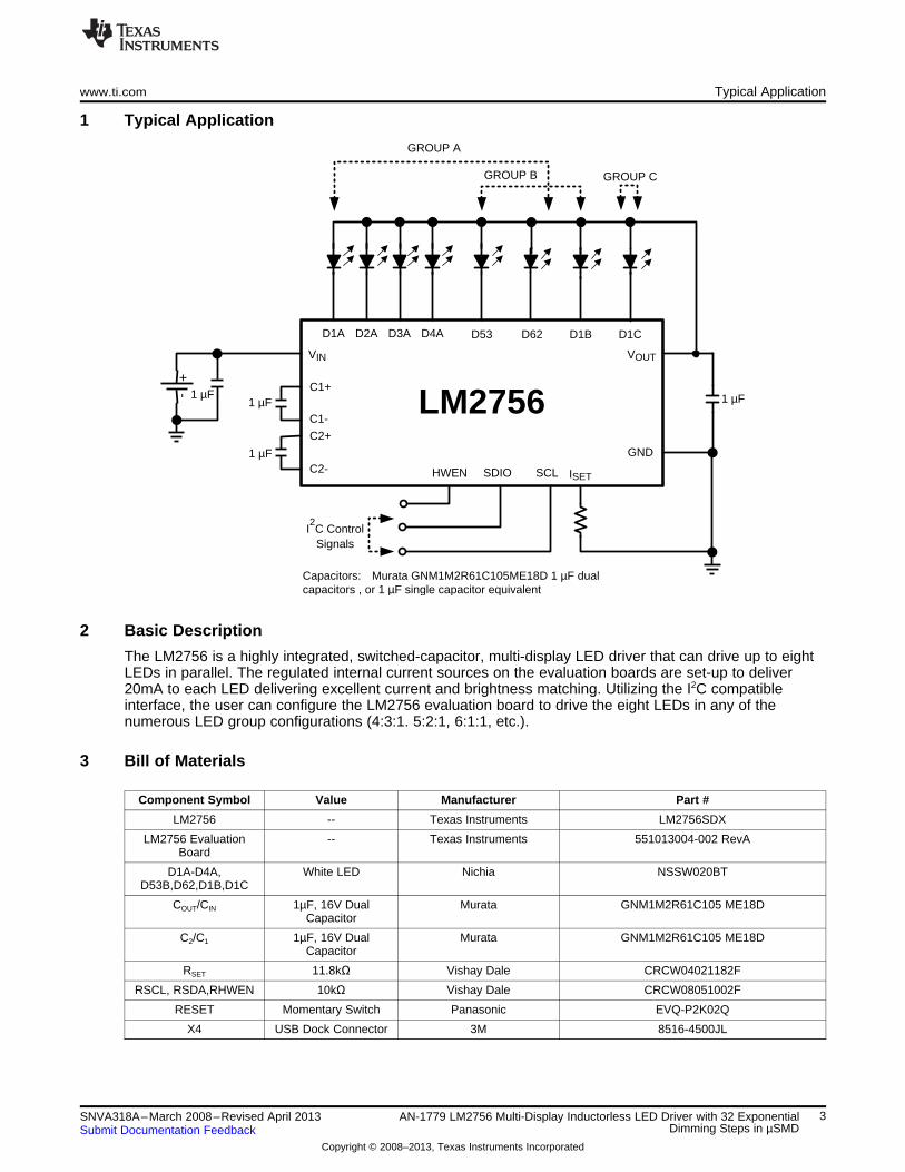
Capacitors: Murata GNM1M2R61C105ME18D 1 µF dual capacitors , or 1 µF single capacitor equivalent
www.ti.com Typical Application
1 Typical Application
2 Basic Description
The LM2756 is a highly integrated, switched-capacitor, multi-display LED driver that can drive up to eightLEDs in parallel. The regulated internal current sources on the evaluation boards are set-up to deliver20mA to each LED delivering excellent current and brightness matching. Utilizing the I2C compatibleinterface, the user can configure the LM2756 evaluation board to drive the eight LEDs in any of thenumerous LED group configurations (4:3:1. 5:2:1, 6:1:1, etc.).
3 Bill of Materials
Component Symbol Value Manufacturer Part #
LM2756 -- Texas Instruments LM2756SDX
LM2756 Evaluation -- Texas Instruments 551013004-002 RevABoard
D1A-D4A, White LED Nichia NSSW020BTD53B,D62,D1B,D1C
COUT/CIN 1µF, 16V Dual Murata GNM1M2R61C105 ME18DCapacitor
C2/C1 1µF, 16V Dual Murata GNM1M2R61C105 ME18DCapacitor
RSET 11.8kΩ Vishay Dale CRCW04021182F
RSCL, RSDA,RHWEN 10kΩ Vishay Dale CRCW08051002F
RESET Momentary Switch Panasonic EVQ-P2K02Q
X4 USB Dock Connector 3M 8516-4500JL
3SNVA318A–March 2008–Revised April 2013 AN-1779 LM2756 Multi-Display Inductorless LED Driver with 32 ExponentialDimming Steps in µSMDSubmit Documentation Feedback
Copyright © 2008–2013, Texas Instruments Incorporated

LM2756 Evaluation Board Schematic www.ti.com
4 LM2756 Evaluation Board Schematic
5 LM2756 Evaluation Board Layout
Figure 1. Top Layer
4 AN-1779 LM2756 Multi-Display Inductorless LED Driver with 32 Exponential SNVA318A–March 2008–Revised April 2013Dimming Steps in µSMD Submit Documentation Feedback
Copyright © 2008–2013, Texas Instruments Incorporated

www.ti.com LM2756 Evaluation Board Layout
Figure 2. Middle Layer 1
Figure 3. Middle Layer 2
Figure 4. Bottom Layer (unmirrored)
5SNVA318A–March 2008–Revised April 2013 AN-1779 LM2756 Multi-Display Inductorless LED Driver with 32 ExponentialDimming Steps in µSMDSubmit Documentation Feedback
Copyright © 2008–2013, Texas Instruments Incorporated

Board Operation www.ti.com
6 Board Operation
6.1 Basic Connections
To operate the LM2756 Multi-Display Inductorless LED Driver with 32 Exponential Dimming Steps inµSMD, connect a supply voltage (2.7V-5.5V) between board connectors VIN and GND and attach an I2Cinterface using one of the methods described in . There is a RESET button provided on the board toexercise the RESET pin on the LM2756. By default, this pins is pulled high through a resistor to allownormal operation. Depressing this button during board operation will shutdown the LM2756 and will clearall of the internal registers resetting them to their default values.
Default Jumper Connections:
• EN_LEDS: This connects VOUT to the anodes of the LEDs. Removing the jumper disconnects the on-board LED power and allows external diodes / measurement equipment to be connected betweenVOUT and the Dx Pins
• VIN_CON: Connects the adjustable voltage supply of the USB Docking board to the VIN of theLM2756. If the USB board is not used, this jumper does not need to be placed. If the USB Dockingboard is going to be used for the I2C interface, but not for VIN, make sure the VIN_CON jumper isremoved.
With the default jumper connections made, the board will be ready to operate once an input voltage andan I2C interface generator (external or USB docking board) are connected.
6.2 External Control Interface Connection
The LM2756 evaluation board provides two ways to connect an I2C compatible interface to the LM2756IC. The first method to connect the interface is through a set of connectors on the bottom of the evaluationboard that allow the board to plug into TI's USB interface board directly. The second method of interfaceconnection is through a header strip located on the left hand side of the evaluation board. There are pinsavailable to connect VIO (controller reference voltage), SCL (Interface Clock Line), and SDA (InterfaceData Line) each separated by a ground pin. The evaluation board has two external pull-ups that connectboth SCL and SDA to VIO to compliment the open drain inputs found on the LM2756. Section 6.3describes the internal registers and I2C compatible interface in greater detail.
6.3 Operation Description
6.3.1 I2C Compatible Interface
6.3.1.1 Data Validity
The data on SDIO line must be stable during the HIGH period of the clock signal (SCL). In other words,state of the data line can only be changed when SCL is LOW.
Figure 5. Data Validity Diagram
A pull-up resistor between the controller's VIO line and SDIO must be greater than [ (VIO-VOL) / 3.5mA ] tomeet the VOL requirement on SDIO. Using a larger pull-up resistor results in lower switching current withslower edges, while using a smaller pull-up results in higher switching currents with faster edges.
6 AN-1779 LM2756 Multi-Display Inductorless LED Driver with 32 Exponential SNVA318A–March 2008–Revised April 2013Dimming Steps in µSMD Submit Documentation Feedback
Copyright © 2008–2013, Texas Instruments Incorporated

www.ti.com Board Operation
6.3.1.2 Start and Stop Conditions
START and STOP conditions classify the beginning and the end of the I2C session. A START condition isdefined as SDIO signal transitioning from HIGH to LOW while SCL line is HIGH. A STOP condition isdefined as the SDIO transitioning from LOW to HIGH while SCL is HIGH. The I2C master alwaysgenerates START and STOP conditions. The I2C bus is considered to be busy after a START conditionand free after a STOP condition. During data transmission, the I2C master can generate repeated STARTconditions. First START and repeated START conditions are equivalent, function-wise.
Figure 6. Start and Stop Conditions
6.3.1.3 Transferring Data
Every byte put on the SDIO line must be eight bits long, with the most significant bit (MSB) transferredfirst. Each byte of data has to be followed by an acknowledge bit. The acknowledge related clock pulse isgenerated by the master. The master releases the SDIO line (HIGH) during the acknowledge clock pulse.The LM2756 pulls down the SDIO line during the 9th clock pulse, signifying an acknowledge. The LM2756generates an acknowledge after each byte is received.
After the START condition, the I2C master sends a chip address. This address is seven bits long followedby an eighth bit which is a data direction bit (R/W). The LM2756 address is 36h. For the eighth bit, a “0”indicates a WRITE and a “1” indicates a READ. The second byte selects the register to which the data willbe written. The third byte contains data to write to the selected register.
w = write (SDIO = "0")r = read (SDIO = "1")ack = acknowledge (SDIO pulled down by either master or slave)id = chip address, 36h for LM2756
Figure 7. Write Cycle
6.3.1.4 I2C Compatible Chip Address
The chip address for LM2756 is 0110110, or 36h.
Figure 8. Chip Address
7SNVA318A–March 2008–Revised April 2013 AN-1779 LM2756 Multi-Display Inductorless LED Driver with 32 ExponentialDimming Steps in µSMDSubmit Documentation Feedback
Copyright © 2008–2013, Texas Instruments Incorporated

Board Operation www.ti.com
6.3.1.5 Internal Registers of LM2756
Register Internal Hex Address Power On Value
General Purpose Register 10h 0000 0000
Group A Brightness Control Register A0h 1110 0000
Group B Brightness Control Register B0h 1111 1000
Group C Brightness Control Register C0h 1111 1000
Ramp Step Time Register 20h 1111 0000
VF Monitor Delay Ragister 60h 1111 1100
Figure 9. General Purpose Register DescriptionInternal Hex Address: 10h
NOTE: ENA: Enables DxA LED drivers (Main Display)
ENB: Enables DxB LED drivers (Aux Lighting)
ENC: Enables D1C LED driver (Indicator Lighting)
SD53: Shuts down driver D53
SD62: Shuts down driver D62
53A: Configures D53 to GroupA
62A: Configures D62 to GroupA
Figure 10. Brightness Control Register DescriptionInternal Hex Address: 0xA0 (GroupA), 0xB0 (GroupB), 0xC0 (GroupC)
8 AN-1779 LM2756 Multi-Display Inductorless LED Driver with 32 Exponential SNVA318A–March 2008–Revised April 2013Dimming Steps in µSMD Submit Documentation Feedback
Copyright © 2008–2013, Texas Instruments Incorporated

www.ti.com Board Operation
NOTE: DxA4-DxA0, D53, D62: Sets Brightness for DxA pins (GroupA). 11111=Fullscale
DxB2-DxB0: Sets Brightness for DxB pins (GroupB). 111=Fullscale
DxC2-DxC0: Sets Brightness for D1C pin. 111 = Fullscale
Full-Scale Current set externally by the following equation:
IDxx = 189 × 1.25V / RSET
Table 1. Brightness Level Control Table (GroupA)
Brightness Code (hex) Perceived Brightness Level (%)
00 0.125
01 0.313
02 0.625
03 1
04 1.125
05 1.313
06 1.688
07 2.063
08 2.438
09 2.813
0A 3.125
0B 3.75
0C 4.375
0D 5.25
0E 6.25
0F 7.5
10 8.75
11 10
12 12.5
13 15
14 16.875
15 18.75
16 22.5
17 26.25
18 31.25
19 37.5
1A 43.75
1B 52.5
1C 61.25
1D 70
1E 87.5
1F 100
9SNVA318A–March 2008–Revised April 2013 AN-1779 LM2756 Multi-Display Inductorless LED Driver with 32 ExponentialDimming Steps in µSMDSubmit Documentation Feedback
Copyright © 2008–2013, Texas Instruments Incorporated

1bit7
1bit6
1bit5
1bit4
1bit3
1bit2
VF1bit1
VF0bit0
MSB LSBVF Monitor Delay Register Register Address: 0x60
1bit7
1bit6
1bit5
1bit4
0bit3
0bit2
RS1bit1
RS0bit0
MSB LSBRamp Step Time Register Register Address: 0x20
Board Operation www.ti.com
GroupB and GroupC Brightness Levels (% of Full-Scale) = 10%, 20%, 30%, 40%, 50%, 60%, 70%, 100%
Figure 11. Ramp Step Time Register Description Internal Hex Address: 20h
NOTE: RS1-RS0: Sets Brightness Ramp Step Time. The Brightness ramp settings only affectGroupA current sinks. ('00' = 100µs, '01' = 25ms, '10' = 50ms, '11' = 100ms).
Figure 12. VF Monitor Delay Register Description Internal Hex Address: 60h
NOTE: VF1-VF0: Sets the Gain Transition Delay Time. The VF Monitor Delay can be set to fourdifferent delay times. ('00' (Default) = 3-6msec., '01' = 1.5-3msec., '10' = 0.4msec., '11' = 60-90µsec.).
6.3.2 LED Configurations
The LM2756 has a total of eight current sinks capable of sinking 180mA of total diode current. These 8current sinks are configured to operate in three independently controlled lighting regions. GroupA has fourdedicated current sinks, while GroupB and GroupC each have one. To add greater lighting flexibility, theLM2756 has two additional drivers (D53 and D62) that can be assigned to either GroupA or GroupBthrough a setting in the general purpose register.
At start-up, the default condition is four LEDs in GroupA, three LEDs in GroupB and a single LED inGroupC (NOTE: GroupC only consists of a single current sink (D1C) under any configuration). Bits 53Aand 62A in the general purpose register control where current sinks D53 and D62 are assigned. By writinga '1' to the 53A or 62A bits, D53 and D62 become assigned to the GroupA lighting region. Writing a '0' tothese bits assigns D53 and D62 to the GroupB lighting region. With this added flexibility, the LM2756 iscapable of supporting applications requiring 4, 5, or 6 LEDs for main display lighting, while still providingadditional current sinks that can be used for a wide variety of lighting functions.
6.3.3 Setting Led Current
The current through the LEDs connected to DxA and DxB can be set to a desired level simply byconnecting an appropriately sized resistor (RSET) between the ISET pin of the LM2756 and GND. The DxA,DxB and D1C LED currents are proportional to the current that flows out of the ISET pin and are a factor of189 times greater than the ISET current. The feedback loops of the internal amplifiers set the voltage of theISET pin to 1.25V (typ.). The statements above are simplified in the equations below:
IDxA/B/C (A)= 189 × (VISET / RSET) RSET (Ω)= 189 × (1.25V / IDxA/B/C) (1)
Once the desired RSET value has been chosen, the LM2756 has the ability to internally dim the LEDs usinganalog current scaling. The analog current level is set through the I2C compatible interface. LEDsconnected to GroupA can be dimmed to 32 different levels. GroupB and GroupC(D1C) have 8 analogcurrent levels.
Please refer to Section 6.3.1 for detailed instructions on how to adjust the brightness control registers.
10 AN-1779 LM2756 Multi-Display Inductorless LED Driver with 32 Exponential SNVA318A–March 2008–Revised April 2013Dimming Steps in µSMD Submit Documentation Feedback
Copyright © 2008–2013, Texas Instruments Incorporated

www.ti.com Software Interface Information
6.3.4 LED Current Ramping
The LM2756 provides an internal LED current ramping function that allows the GroupA LEDs to turn onand turn off gradually over time. The target current level is set in the GroupA Brightness Control Register(0xA0). The total ramp-up/ramp-down time is determined by the GroupA brightness level (0-31) and theuser configurable ramp step time.
Bits RS1 and RS2 in the Ramp Step Time Register (0x20) set the ramp step time to the following fourtimes: '00' = 100µsec., '01' = 25msec., '10' = 50msec., '11' = 100msec.
The LM2756 will always ramp-up (upon enable) and ramp-down (upon disable) through the brightnesslevels until the target level is reached. At the default setting of '00', the LM2756's current ramping featurelooks more like a current step rather than a current ramp. Table 2 the approximate ramp-up/ramp-downtimes if the GroupA brightness register is set to full-scale, or brightness code 31.
Table 2. Brightness Ramp-Up/Ramp-Down Times
Ramp Code Ramp Step Total RampRS1-RS0 Time Time
00 100µs 3.2ms
01 25ms 0.8s
10 50ms 1.6s
11 100ms 3.2s
7 Software Interface Information
In order to fully evaluate the LM2756 part, an I2C Compatible interface must be used for any functionalityto occur. A detailed description of the interface control is described in the LM2756 data sheet.
Texas Instruments has created an I2C compatible interface generation program and USB docking boardthat can help exercise the part in a simple way. Contained in this document is a description of how to usethe USB docking board and interface software.
The LM2756 evaluation board has the means to “plug into” the USB docking board. The USB dockingboard can provide all of the control signals and power required to operate the evaluation board. Astandard USB cable must be connected to the board from a PC.
The I2C compatible interface program provides all of the control that the LM2756 part requires. For properoperation, the USB docking board should be plugged into the PC before the interface program is opened.Once connected, and the program is executed, a basic interface window will open.
Figure 13. GUI Start-Up
11SNVA318A–March 2008–Revised April 2013 AN-1779 LM2756 Multi-Display Inductorless LED Driver with 32 ExponentialDimming Steps in µSMDSubmit Documentation Feedback
Copyright © 2008–2013, Texas Instruments Incorporated

Software Interface Information www.ti.com
At the top of the interface, the user can read or write to any of the data registers on the LM2756 part usingthe two pull down menus (for the slave i.d. and the desired data address), the data field, and the read andwrite buttons.
Figure 14. Generic Read/Write Field
Figure 15. Drop Down Menu
Just below the pull down menus are convenient toggle buttons to set/reset the control bits in the GeneralPurpose Register.
Figure 16. Control and Configuration Buttons
• 62toA and 53toA: Assigns D62 and D63 current sinks to BankA when depressed. By default, D62 andD53 are assigned to BankB
• SD62 and SD53: Disabled drivers D62 and D53 when depressed
• ENC, ENB and ENA: These bits, when depressed, enable BankA, BankB and BankC.
Figure 17. Brightness Control Sliders
• BankA Slider: Sets the BankA brightness to any allowable brightness code (0 to 31)
• BankB Slider: Sets the BankB brightness to any allowable brightness code (0 to 7)
• BankCSlider: Sets the BankC brightnessn to any allowable brightness code (0 to 7)
12 AN-1779 LM2756 Multi-Display Inductorless LED Driver with 32 Exponential SNVA318A–March 2008–Revised April 2013Dimming Steps in µSMD Submit Documentation Feedback
Copyright © 2008–2013, Texas Instruments Incorporated

www.ti.com Software Interface Information
Figure 18. BankA Ramp Step Time
• Ramp Step Time: This field sets the BankA brightness control ramp-up/ramp-down times. The timeshown in the field corresponds to the time the LM2756 remains at each brightness code.
Figure 19. Results of Pressing the Set Button
Pressing the Set button places the LM2756 into the 4:3:1 configuration and sets the brightness levels ineach bank to full-scale.
Figure 20. Example Configuration
In this configuration, the LM2756 will have 6 LEDs in BankA set to the full-scale brightness with a rampstep time equal to 13ms. BankB and BankC are each set to brightness code3 and are both active.
13SNVA318A–March 2008–Revised April 2013 AN-1779 LM2756 Multi-Display Inductorless LED Driver with 32 ExponentialDimming Steps in µSMDSubmit Documentation Feedback
Copyright © 2008–2013, Texas Instruments Incorporated

Software Interface Information www.ti.com
NOTE: If the part is enabled to any level of brightness or state and the program is closed (by eitherhitting the OK or cancel buttons) , the LM2756 part will remain in the last controlled state.
14 AN-1779 LM2756 Multi-Display Inductorless LED Driver with 32 Exponential SNVA318A–March 2008–Revised April 2013Dimming Steps in µSMD Submit Documentation Feedback
Copyright © 2008–2013, Texas Instruments Incorporated

IMPORTANT NOTICE
Texas Instruments Incorporated and its subsidiaries (TI) reserve the right to make corrections, enhancements, improvements and otherchanges to its semiconductor products and services per JESD46, latest issue, and to discontinue any product or service per JESD48, latestissue. Buyers should obtain the latest relevant information before placing orders and should verify that such information is current andcomplete. All semiconductor products (also referred to herein as “components”) are sold subject to TI’s terms and conditions of salesupplied at the time of order acknowledgment.
TI warrants performance of its components to the specifications applicable at the time of sale, in accordance with the warranty in TI’s termsand conditions of sale of semiconductor products. Testing and other quality control techniques are used to the extent TI deems necessaryto support this warranty. Except where mandated by applicable law, testing of all parameters of each component is not necessarilyperformed.
TI assumes no liability for applications assistance or the design of Buyers’ products. Buyers are responsible for their products andapplications using TI components. To minimize the risks associated with Buyers’ products and applications, Buyers should provideadequate design and operating safeguards.
TI does not warrant or represent that any license, either express or implied, is granted under any patent right, copyright, mask work right, orother intellectual property right relating to any combination, machine, or process in which TI components or services are used. Informationpublished by TI regarding third-party products or services does not constitute a license to use such products or services or a warranty orendorsement thereof. Use of such information may require a license from a third party under the patents or other intellectual property of thethird party, or a license from TI under the patents or other intellectual property of TI.
Reproduction of significant portions of TI information in TI data books or data sheets is permissible only if reproduction is without alterationand is accompanied by all associated warranties, conditions, limitations, and notices. TI is not responsible or liable for such altereddocumentation. Information of third parties may be subject to additional restrictions.
Resale of TI components or services with statements different from or beyond the parameters stated by TI for that component or servicevoids all express and any implied warranties for the associated TI component or service and is an unfair and deceptive business practice.TI is not responsible or liable for any such statements.
Buyer acknowledges and agrees that it is solely responsible for compliance with all legal, regulatory and safety-related requirementsconcerning its products, and any use of TI components in its applications, notwithstanding any applications-related information or supportthat may be provided by TI. Buyer represents and agrees that it has all the necessary expertise to create and implement safeguards whichanticipate dangerous consequences of failures, monitor failures and their consequences, lessen the likelihood of failures that might causeharm and take appropriate remedial actions. Buyer will fully indemnify TI and its representatives against any damages arising out of the useof any TI components in safety-critical applications.
In some cases, TI components may be promoted specifically to facilitate safety-related applications. With such components, TI’s goal is tohelp enable customers to design and create their own end-product solutions that meet applicable functional safety standards andrequirements. Nonetheless, such components are subject to these terms.
No TI components are authorized for use in FDA Class III (or similar life-critical medical equipment) unless authorized officers of the partieshave executed a special agreement specifically governing such use.
Only those TI components which TI has specifically designated as military grade or “enhanced plastic” are designed and intended for use inmilitary/aerospace applications or environments. Buyer acknowledges and agrees that any military or aerospace use of TI componentswhich have not been so designated is solely at the Buyer's risk, and that Buyer is solely responsible for compliance with all legal andregulatory requirements in connection with such use.
TI has specifically designated certain components as meeting ISO/TS16949 requirements, mainly for automotive use. In any case of use ofnon-designated products, TI will not be responsible for any failure to meet ISO/TS16949.
Products Applications
Audio www.ti.com/audio Automotive and Transportation www.ti.com/automotive
Amplifiers amplifier.ti.com Communications and Telecom www.ti.com/communications
Data Converters dataconverter.ti.com Computers and Peripherals www.ti.com/computers
DLP® Products www.dlp.com Consumer Electronics www.ti.com/consumer-apps
DSP dsp.ti.com Energy and Lighting www.ti.com/energy
Clocks and Timers www.ti.com/clocks Industrial www.ti.com/industrial
Interface interface.ti.com Medical www.ti.com/medical
Logic logic.ti.com Security www.ti.com/security
Power Mgmt power.ti.com Space, Avionics and Defense www.ti.com/space-avionics-defense
Microcontrollers microcontroller.ti.com Video and Imaging www.ti.com/video
RFID www.ti-rfid.com
OMAP Applications Processors www.ti.com/omap TI E2E Community e2e.ti.com
Wireless Connectivity www.ti.com/wirelessconnectivity
Mailing Address: Texas Instruments, Post Office Box 655303, Dallas, Texas 75265Copyright © 2013, Texas Instruments Incorporated