amplifier analysis aind design
TRANSCRIPT

ESD-TR-88-181
Technical Report 812
Amplifier Analysis aind Design
L.J. Kushner
U December 1988
Lincoln Lab#$ MASSACHUSETTS THSTFTOtE
LEXINGTON, MASSA*
Prepared under Electronic S$*fe*^]fc
Approved lor public releaie;
ft DP *•«>■*'^

The work reported in this document was performed at Lincoln Laboratory, a center for research operated by Massachusetts Institute of Technology, with the support of the Department of the Army under Air Force Contract F19628-85-C-0002.
This report may be reproduced to satisfy needs of U.S. Government agencies.
The views and conclusions contained in this document are those of the contractor and should not be interpreted as necessarily representing the official policies, either expressed or implied, of the United States Government.
The ESD Public Affairs Office has reviewed this report, and it is releasable to the National Technical Information Service, where it will be available to the general public, including foreign nationals.
This technical report ha« been reviewed and is approved for publication.
FOR THE COMMANDER
Hugh L. Southall, hi. €ol.t USAF Chief, ESD Lincoln Laboratory Project Office
Non-Lincoln
PLEASE DO HOT RETURN
Permission is given to destroy this document when it is no longer needed.
MASSACHUSETTS INSTITUTE OF TECHNOLOGY LINCOLN LABORATORY
MICROWAVE POWER AMPLIFIER ANALYSIS AND DESIGN
LJ. KUSHNER Group 66
TECHNICAL REPORT 812
16 DECEMBER 1988
Approved for public release; distribution unlimited.
LEXINGTON MASSACHUSETTS


ABSTRACT
Output power, efficiency, power dissipation, and optimum load-resistance expressions for idealized microwave Class A and B power amplifiers are derived based on a waveform analysis. The effects of device transconductance variation with bias and circuit harmonic termination are examined. Large-signal gain is determined by calculating the input power needed to produce a given output power. Both closed-form and CAD-based solutions are presented, all based on device de I-V characteristics and small-signal models. A practical power amplifier design procedure is given and used to design a 22-GHz permeable-based transistor (PBT) power amplifier. Although the analysis and design results presented here are useful by themselves, they are also intended to be used in conjunction with other CAD and measurement techniques (such as harmonic balance and load pull) to arrive at a starting point. Device designers also should find these results useful, allowing them to predict how changes in device parameters will affect microwave power amplifier performance.
in


TABLE OF CONTENTS
Abstract iii List of Illustrations vii List of Tables vii Acknowledgments ix
1. INTRODUCTION 1
2. OUTPUT POWER AND EFFICIENCY CALCULATIONS 3
2.1 Current Waveforms 3 2.2 Voltage Waveforms, Output Power, Efficiency, Power
Dissipation, and Load Resistance 8
3. LARGE-SIGNAL GAIN 19
3.1 Input Power and Large-Signal Gain Calculation 19 3.1.1 Closed-Form Expressions for Input Power 21 3.1.2 A Fast and Simple Computer-Aided Method of
Calculating Input Power 25
3.2 Effect of Small-Signal Output Impedance on Large-Signal Gain 27
4. LOAD-LINE SELECTION AND MATCHING NETWORK DESIGN 31
4.1 Load-Line Selection 31 4.2 Matching Network Design 34 4.3 Large-Signal Performance Estimation and Verification 38
5. CONCLUSIONS 39
References 41


LIST OF ILLUSTRATIONS
Figure No. Page
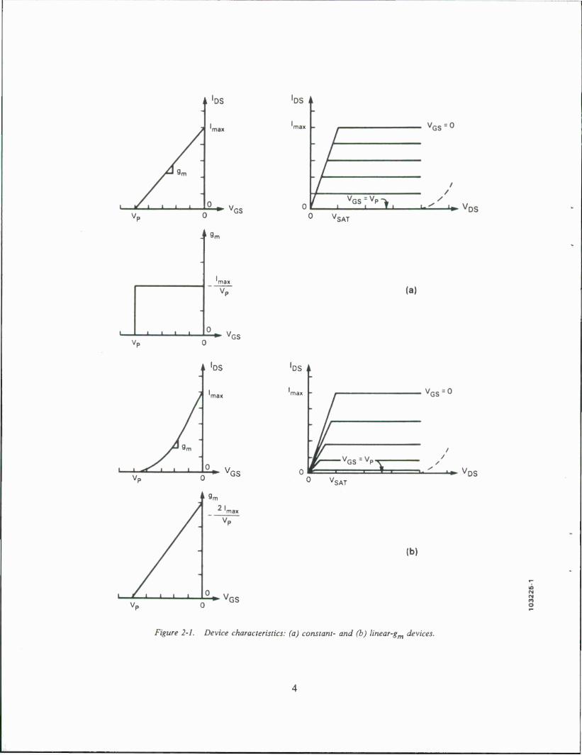
2-1 Device characteristics: (a) constant- and (b) linear-gm devices 4
2-2 Load circuits: (a) resistive and (b) tuned loads 5
2-3(a) Amplifier waveforms: constant-gm devices 6
2-3(b) Amplifier waveforms: linear-gm devices 7
2-4 (a) Load-line selection, (b) effect on drain-source current, and (c) voltage 11
3-1 Large-signal gain calculation: (a) determining control voltage |V| needed to produce Pout, and (b) determining Pin needed to produce |V| 19
3-2 Simple device input model 21
3-3 Device input model extended to include common-lead impedance 22
3-4 Device input model extended to include feedback capacitance: (a) original and (b) equivalent models 25
3-5 Device input model with 1:1 transformer added for CAD analysis 26
3-6 Effect of finite output impedance 29
4-1 Load-lines: (a) constant- and (b) linear gm devices 32
4-2 PBT I-V characteristics and load-lines (wafer 2P23A, 1 X 1 device) 33
4-3 Matching circuits: (a) input and (b) output 35
4-4(a) PBT amplifier output matching circuit: fundamental-frequency (22-GHz) design 36
4-4(b) PBT amplifier output matching circuit: second-harmonic (44-GHz) impedance 37
LIST OF TABLES
Table No. Page
2-1 Fourier analysis of drain-source-current waveforms 8
2-2 Class A and B power amplifier performance (VDD < VDDmax) 14
2-3 Class A and B power amplifier performance (VDD = VDDmax) 16
3-1 Gain degradation in scaled PBTs due to fixed common-lead impedance 24
vii


ACKNOWLEDGMENTS
This work grew out of discussions with Mark Hollis, Rick Mathews, Al Murphy, Carl Bozler, and Kirby Nichols in our search for better PBTs. Discussions with Bill Courtney were most helpful, and his research was the basis for the gain calculations of Section 3. The author would like to thank Dave Snider and Ron Bauer for their interest in this work and for provid- ing the time needed to complete it.
IX


MICROWAVE POWER AMPLIFIER ANALYSIS AND DESIGN
1. INTRODUCTION
Given the variety of microwave nonlinear computer-aided design (CAD) programs available today, such as the time-domain program SPICE (developed at the University of California, Berkeley), and the harmonic-balance programs Libra (EEsof, Inc.) and Microwave Harmonica (Compact Software), one might wonder what good are the relatively simplistic, quasi-static results presented in this report. Assuming that the device in question can adequately fit into their mod- els, one would expect these other more complex analysis methods to provide more accurate results. Unlike the methods presented here, these nonlinear-CAD programs can be used to calcu- late intermodulation performance. However, while great for analysis, these computation-intensive numeric methods provide little insight needed for design. They provide specific results for a given device, but do not show general trends and relationships. In contrast, the results presented in this report are more general, giving a better picture of amplifier operation while requiring far fewer calculations.
Using most CAD programs, designing a circuit is accomplished by repeatedly reanalyzing it after varying some circuit-element values, a procedure usually referred to as "optimization." The better the designer's first guess (initial value), the fewer parameters that are varied, and the more constrained these parameters are, the faster these programs converge to an optimum solution. While important for linear-CAD optimization, a good first guess becomes critical in nonlinear- CAD, due to the required order-of-magnitude increase in computation. The results presented in this report provide a fast and simple method of attaining that all-important initial value, much closer to the ultimate solution than would be obtained by small-signal analysis or by celestial extraction (i.e., pulling numbers out of the air).
The methods presented are sufficient to design many power amplifiers without the need for any additional nonlinear-CAD analysis. Several other power amplifier applications, such as load- pull measurements and empirical amplifier tuning, also benefit from these results. Besides provid- ing a starting point by estimating the output power and gain obtainable from an amplifier, this method also tells you when to stop.
Rather than a numeric-based method, the procedures described below are based primarily on analytical expressions and graphical techniques, leading to better understanding and insight. How a certain parameter will affect amplifier performance is obvious from the derived equations, rather than requiring a whole battery of computer runs. A device designer can use these results to quickly predict the microwave power performance obtainable from a device, rather than wait- ing for circuit design, fabrication, and test.
Output power, efficiency, power dissipation, and optimum load-resistance results are derived in Section 2 based on a waveform analysis. These are essentially the textbook Class A and B power amplifier results for two different device types (constant or linear transconductance) and

two different load circuits (resistive or tuned). Unfortunately, no textbook known to the author covers more than just a few of the simplest cases. (The most complete coverage appears in [1], but this covers just a small subset of the cases presented here.) The derivations presented below attempt to fill this void. All these results are consolidated into three tables for easy reference.
Section 3 combines the output power calculation of Section 2 with an input power calcula- tion to arrive at large-signal gain. Although extended considerably, the basic idea for this gain calculation method came from Courtney and Gopinath [2] who derive some of the same output power and efficiency results presented here, but from a somewhat different approach. Analytical expressions for input power are derived in terms of the device parameters, followed by a novel numeric method of input power calculation employing a linear circuit analysis program, such as Super-Compact (Compact Software). This simple, yet accurate analysis method is probably the most important contribution of this report.
Section 4 pulls all the pieces together and comes up with a straightforward power amplifier design procedure. This method has been used to design a variety of 22-GHz PBT power amplifi- ers (70 to 400 mW) with excellent correlation between predicted and measured responses. One such amplifier design is given as an example.
It should be pointed out that many of the derivations below assume a voltage-controlled device such as an FET, PBT, or HEMT and would have to be modified somewhat to handle current-controlled devices, such as bipolar transistors.

2. OUTPUT POWER AND EFFICIENCY CALCULATIONS
In this section, the output power, drain efficiency, power dissipation, and optimum load resistance (for maximum output power) are calculated for Class A and B power amplifiers based on a waveform analysis and a device's static I-V characteristics While most textbooks derive these results for devices with a constant-transconductance (gm) versus gate-voltage characteristic [Fig- ure 2-1(a)], most real-life devices (such as FETs and PBTs) tend to have control characteristics more closely approximated by a linear-transconductance variation [Figure 2-1(b)]. Furthermore, all the textbook derivations assume a perfect tuned-load circuit [Figure 2-2(b)], while in practice, few microwave amplifiers provide a short circuit to all the harmonic frequencies. These issues are not just theoretical, but have practical implications. Some FET designers have intentionally modi- fied their device doping profiles in an effort to get constant rather than linear-transconductance devices [3], claiming improved output power, gain, and efficiency. Concerning the harmonic ter- mination issue, power amplifier designers should know what penalty they will pay for failing to properly terminate amplifier harmonic frequencies.
The analysis presented derives results for Class A and B amplifiers, with either constant- or linear-gm devices, and with resistive or tuned loads (see Figure 2-2). Note that in all cases, the dc bias to the device is assumed to be brought into the circuit through large dc chokes, and blocked from the load by large coupling capacitors. Besides these simple load types, the basic derivations allow a broader range of load impedances to be evaluated. While infinite device output imped- ance (i.e., flat I-V curves) is assumed for the initial derivations, Section 3 considers the effect of finite output impedance.
2.1 Current Waveforms
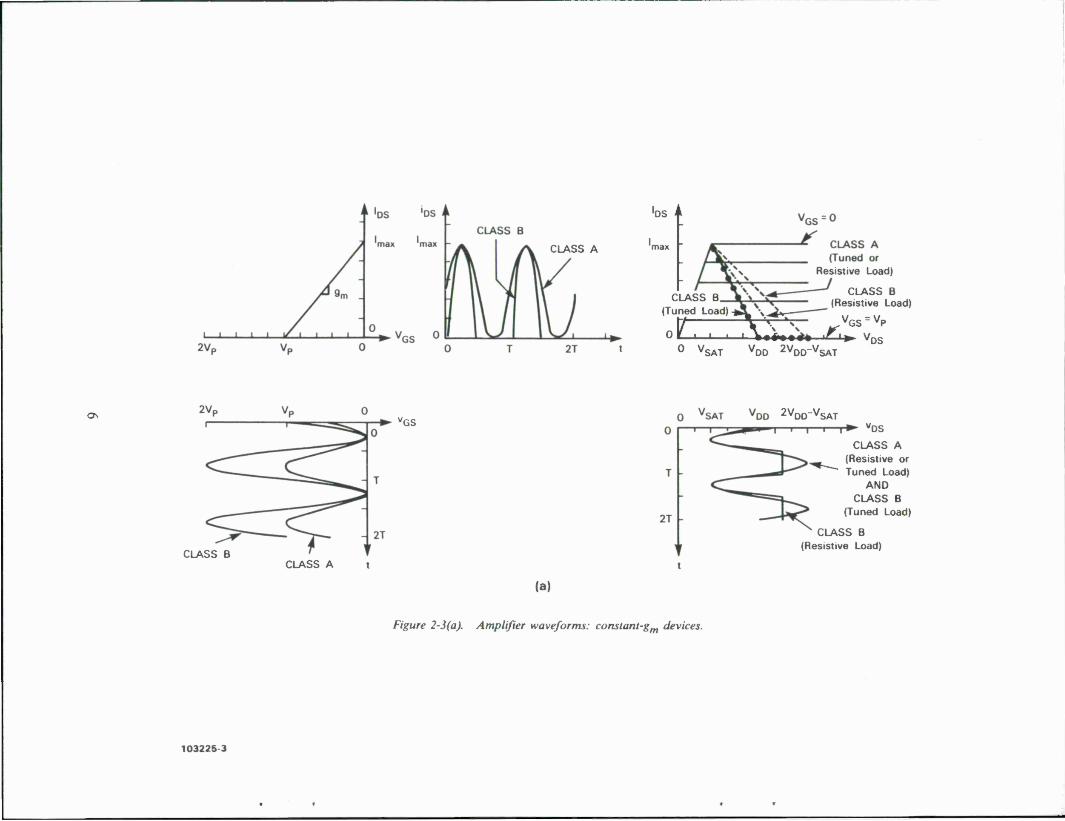
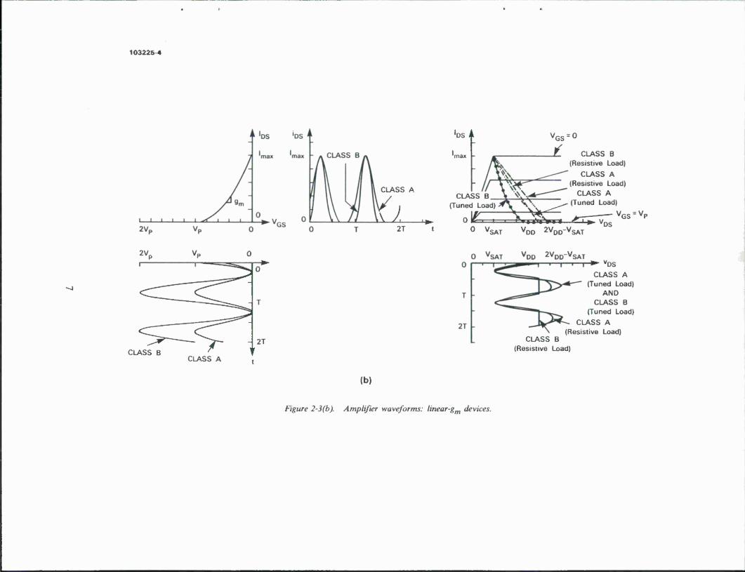
Figure 2-3 contains the input voltage waveforms (vGS), device control characteristics, output current waveforms (ios)> load-lines*, and output voltage waveforms for all the cases considered. For now, only the input voltage and output currents will be discussed. Output voltages and load- lines are addressed later, but are included in this figure for completeness.
As illustrated in Figure 2-3, using the idealized device control characteristics along with sinu- soidal gate-voltage excitations of proper amplitude and offset, device drain currents can be determined for each of the four combinations of transconductance type (constant or linear) and amplifier class (A or B). Notice that iDS is assumed to be independent of vDS, which from Figure 2-1 is seen to be true as long as vDS stays above VSAT and below the device breakdown voltage (VBR).t If the device output impedance were finite rather than infinite as assumed, iDS
would be dependent on vDS, greatly complicating this analysis.
* A plot of the instantaneous drain-source current versus voltage superimposed on the device I-V characteristics.
t More precisely, it is actually the drain-gate voltage that must stay below VBR, but since the gate-source voltage is usually small, vD§ — VDG and the previous statement is approximately cor- rect. This analysis assumes that when the device is pinched-off, drain-gate breakdown is deter- mined solely by the drain-gate voltage, as suggested by Tajima and Miller [4]. Breakdown limita- tions are discussed in greater detail in Section 2.2.
'DS
0 V SAT
(a)
'DS 'DS A
0 V SAT 'DS
(b)
Figure 2-1. Device characteristics: (a) constant- and (b) linear-g devices.

'DO 'DO
to CM CM
O
ZJn] = RL ,n3*1
(a)
ZJn] = RL ,n = 1
0 ,n> 1
(b)
Figure 2-2. Load circuits: (a) resistive and (b) tuned loads.
Two important observations can be made concerning the current waveforms of Figure 2-3. Looking at these drain-source currents for the first time, it is somewhat surprising to see how similar the waveforms are, given that the Class B amplifier only conducts current during half the rf input cycle, while the Class A amplifier conducts during the entire cycle. Current waveforms for an amplifier operating Class AB lie somewhere between these Class A and Class B currents. A more dramatic difference between Class A and B appears in the input (gate-to-source voltage) waveforms. Class B operation requires twice the drive-voltage swing as Class A, resulting in ~6 dB less rf gain. (In reality, gain in Class B operation is not a full 6 dB worse than in Class A, due to the reduced input capacitance at this bias point, and finite device output-impedance.)
Analytic expressions for the current waveforms of Figure 2-3 are easily obtained for each of the four cases:
Class A, constant gm:
Class A, linear gm:
Class B, constant gm:
Class B, linear gm:
iDSl^max/^O + sina'oO
iDS2=(W4)0+sincoot)2
*DS3 =
*DS4
Jmax sin "o*
'max sin2 <M
,0 ^ t ^ T (2.1)
,0 ^ t ^ T (2.2)
,0^t<T/2 (2.3)
,T/2^t^T
,0^t^T/2 (2.4)
,T/2<t^T
CLASS A
(DS A
CLASS B (Tuned Load)
0
Resistive Load)
nitru —! m L < ^- -—
v— \\'*■ t—■—I—I—I »•*•»
CLASS B (Resistive Load)
vGS = vp
0 V SAT VDD 2VDD"VSAT DS
ON
CLASS B
VGS 2VDD-VSAT
CLASS A t
(a)
Figure 2-3(a). Amplifier waveforms: constant-gm devices.
VDS
CLASS A (Resistive or Tuned Load)
AND CLASS B
(Tuned Load)
CLASS B (Resistive Load)
103225 3
103225 4
CLASS A
±2 ^ 2T
DS i\
CLASS B (Tuned Load)
0 V
VGS = 0
L- CLASS B (Resistive Load)
CLASS A (Resistive Load)
CLASS A ^„ (Tuned Load)
_^^\ jr — VGS = VP
SAT /DD 2VDD"VSAT
2Vp VP 0 t
0
^^" T
2T
CLASS B l f
VDD 2VDD-VSAT
T-^ VDS
CLASS A (Tuned Load)
AND CLASS B
(Tuned Load)
CLASS A (Resistive Load)
CLASS B (Resistive Load)
CLASS A
(b)
Figure 2-3(b). Amplifier waveforms: linear-g devices.

Being periodic, each of these waveforms can be expressed as a Fourier series
n = « 'DSW= 2 IDstn] eJ-ot (2.5)
n = -oo
A Fourier analysis was performed on these four current waveforms to determine how much cur- rent flows at each harmonic frequency (Table 2-1). The fundamental component of drain-source current, IDSDL ls tne same f°r Class A (both cases 1 and 2) and Class B/ constant gm (case 3), but is 1.4 dB lower in the class B/ linear gm (case 4). Although the current waveforms of these first three cases have the same fundamental component, significant differences occur in their harmonic contents.
TABLE 2-1
Fourier Analysis of Drain-Source-Current Waveforms
9m
Drain-Source-Current Fourier Components
CASE TYPE los«» IDSH] IDSI2] 'DS^odcT* 1] 'DS^even'* 21
CLASS A
1 Constant 'max
2
'max
4j 0 0 0
2 Linear 3'max
8
'max
4j
'max
16 0 0
CLASS B
3 Constant 'max
7T
'max
4j
'max
3TT 0
'max
TT(1 -n2)
4 Linear 'max
4
2'max
3TTJ
'max
8
2'max 0
J7rn(4 - n2)
2.2 Voltage Waveforms, Output Power, Efficiency, Power Dissipation, and Load Resistance
The current waveforms and Fourier analysis of Section 2.1 can be combined with the load circuits of Figure 2-2 to produce the drain-to-source voltage frequency components, VDS[n], and time waveforms, vDS(t):

VDD ,n = 0 VDstn]=< (2-6)
-IosMZJn] ,n^l
and
n = oo
VDS(0= X VDSW eJn<Bot (2-7)
Notice that Equation (2.6) allows arbitrary load impedances to be connected to the device. This can lead to erroneous conclusions, however, since this result was derived by assuming that the device drain-to-source voltage vDs stays between VSAT and approximately VBR, keeping the drain-to-source current iDS independent of vDS. While this will be true for small load imped- ances, large-impedance loads will cause vDS to swing beyond this region, violating the initial assumption. In particular, the optimum (for maximum output power) fundamental frequency load resistance is selected just large enough so that the device operation swings from saturation to the verge of breakdown. Any larger resistance will cause voltage clipping not modeled by this fre- quency domain analysis. This issue is discussed in greater detail below.
Equation (2.6) requires that the load impedance ZJn] be known before VDS[n] can be determined. To choose the proper load impedance for maximum output power, a digression to discuss output power and load-lines is in order.
The power dissipated by the device can be found in either the time or frequency domains. In the time domain
PDISS = f j iösW vDsW dt (2.8)
By plugging the Fourier series expansions for iosW anc* VDS(
1) [Equations (2.5) and (2.7)] into
Equation (2.8) or by using ParsevaFs Theorem, the dissipated power can also be computed from the frequency domain components
n = oo
PDISS= % IDSW V*DS[n] • (2-9) n = -oo
Since iosW and VDSW
are rea* ^me functions, lost11] and vDs[nl are conjugate symmetric, so Equation (2.9) can be rewritten as:
n = oo
PDISS= 2 PDISSM (2.10) n = 0
where

. IDS[0]VDS[0] ,m = 0 PDISS tm] =
2 Re IDS[m] V*DS[m] ,m^l
In Equation (2.10), VDS[0] is the supply voltage VDD, while Iost^l *s tne ^me average value of the ipsW waveform as determined by the device bias point, the input signal drive level, and the waveform shape. If the device delivers, rather than dissipates, power at a frequency ma>0, PDISSC111] < 0, and the output power at that frequency is given by
Pouttm] = -PDISSM = "2 Re {IDSM V*DS[in]} ,m > 1 . (2.11)
In order to maximize output power, the phases of VDS[m] and lost01! are made 180° apart, reducing the expression for Pout[m] to
PoutM = 2 |IDS[m] | |VDS[m] |, for ZIDS[m] - ZVDS[m] = 180° ,m ^ 1 (2.12)
From Equation (2.12), it is obvious that Pout[m] is further maximized by maximizing the magni- tudes of IDSC111] ana< VDS[m]. For the device without parasitics considered to this point, the 180° phase condition is met by using a purely real (i.e., no reactive component) load impedance RL, and the magnitude condition is met by choosing the optimum load-line, as illustrated in Fig- ure 2-4 (for the simple constant gm, Class A amplifier case). By choosing the load-line to go through the points (VSAT,Imax) and (2VDD - VSAT,0), voltage swing AV and current swing AI are both maximized for a given supply voltage, VDD. This load-line is traversed by biasing the device at (VDD,Imax/2) and by setting RL equal to AV/AI = 2(VDD - VSAT)/Imax = RLopt. Choosing RL < R^pt results in the same current swing [Figure 2-4(b)], but reduced voltage swing [Figure 2-4(c)], while choosing RL > RLopt results in approximately the same voltage swing (assuming 2VDD - VSAT =* VBR), but reduced current swing. In other words, by picking the load- line to simultaneously maximize both AV and AI, output power is maximized.! This explains why a load circuit designed for maximum small-signal gain almost always results in suboptimal power performance. In order to achieve maximum small-signal gain, RL is chosen to be equal to the device incremental output resistance which, in general, is much larger than RLopt (especially for a high-current power device). This choice of RL results in the full voltage swing, AV — VBR - VSAT, but AI much less than Imax.
f An interesting argument can be made concerning the choice or RL. If RL is increased beyond RLopt> vDs(t) begins to become clipped, but its fundamental component VDsni continues to increase beyond that obtained when RL = RLopt- Meanwhile, IDS^ begins to decrease. If Ips^ could somehow be kept from dropping faster than VDsn] increases, output power would continue to increase as RL is increased beyond RLopt- While further discussion is beyond the scope of this report, the reader is referred to [5] and [6] for more details.
10

£VGS = 0
RL > RLopt
0 V SAT VDD 2VDO-VSAT 'OS
(a)
■DS A
RL ^ RLopt
RL > RLopt
2VDD-VSAT
2vDD-vSAT<vBRn
2VDD-VSAT-VBR
RL = RLopt
RL > RLopt
RL < RLopt
*-► t
Figure 2-4. (a) Load-line selection, (b) effect on drain-source current, and (c) voltage.
11

While Equations (2.10) through (2.12) are quite useful in picking the load resistance, for further calculations it is more convenient to express power in terms of current and load impe- dance rather then current and voltage. From Equation (2.6), VDS[n] = -IosM ZJn] for n >1, and assuming that ZL[n] is conjugate symmetric, Equation (2.9) can be rewritten as
PDISS = IDSEO] VDS[0] - 2^ HDSM I2 Re {ZL[n]} . (2.13) n = 0
This expression is the dc power into the device minus the sum of the ac powers delivered to the load, i.e.,
PDISS = PDC- *2 PoutM (214a> n = 0
where
and
PDC = IDS[0]VDD (2.14b)
Pouttn] = 21 IDS[n] 12 Re {ZJn]} (2.14c)
= power delivered to load at nth harmonic
Before leaving the subject of output power, two definitions are given:
drain efficiency = r7D = PoutHl/PDC <2-15)
power-added efficiency = 77add = T7D (1 - 1/G) . (2.16)
The term "G" in Equation (2.16) is large-signal gain of the amplifier. Notice that ?7add < TJD, with equality being approaches in the limit as G approaches infinity. Since Section 3 is devoted to the calculation of large-signal gain, G will not be discussed further here.
Having determined that output power is maximized by selecting the load resistance to max- imize both current and voltage swings, the output-voltage waveforms can now be determined, along with expressions for output power (at the fundamental and harmonic frequencies), power dissipation, drain efficiency, and optimum load resistance:
0) ^DsW an<* ^Dstnl are determined from Equations (2.1) through (2.4) and Table 2-1, respectively, once the amplifier Class (A or B) and transconduc- tance variation (constant or linear) have been selected. It is assumed that R-L < ^Lopt» so current swing is at its maximum.
(2) Analytical expressions for VDS[n] in terms of ZL[n] are determined from Equation (2.6).
(3) vDS(t) is obtained from Equation (2.7).
12

(4) RL is chosen so that the minimum value of vDS(t) is equal to VSAT. This provides the maximum possible voltage swing for a given supply voltage and waveform shape, assuming the device is operating below breakdown. Since maximum current swing was already assumed, this value of RL corresponds to R.Lopt» giving maximum output power.
(5) Output power (fundamental and harmonics) and dissipated power are calcu- lated from Equations (2.14c) and (2.14a), respectively.
(6) Drain efficiency is determined from Equation (2.15).
The above procedure was used to analyze Class A and B amplifiers with either constant- or linear-transconductance devices, and with resistive or tuned loads. The results of this analysis are given in Table 2-2. While the above procedure goes from the time domain iosW to tne frequency domain Ios[n] and vDstn] an(* back to the time-domain vDS(t), the same results can be obtained by an alternative equivalent method for the case of these simple resistive and tuned loads. Due to the simple nature of the loads considered, the form of the time-domain voltage vDS(t) can be determined by inspection, and the frequency-domain components VDS[n] can be obtained by a Fourier analysis of vDS(t). However, any load circuit more complex than a resistive or tuned load cannot easily be handled by this alternative method, while the procedure detailed above has no problem handling more general load impedances.
Several important observations can be made from Table 2-2:
(1) In all cases, drain efficiency is degraded by the term a = (VDD - VSAT)/VDD. Clearly, the larger the supply voltage VDD is relative to the saturation voltage VSAT the better the efficiency. Unfortunately, VDD cannot be increased with- out limit due to drain-gate breakdown, excessive power dissipation in the device, and gain reduction at higher operating voltages. These issues are dis- cussed in more detail below.
(2) For Class A operation, linear- rather than constant-gm is preferable, as long as a tuned load can be implemented. In this case (2b), output power remains the same as in the constant-gm device, but drain efficiency improves from 50 to 67 percent. Terminating the harmonics resistively (cases la and 2a) rather than shorting them to ground (cases lb and 2b) results in a decrease in both output-power and efficiency for the linear-gm device, but has no effect on the constant-gm device (as expected, since in cases la and lb, no harmonics are generated).
(3) In Class B operation, better output power is achieved with constant- than with linear-gm devices, for both resistive and tuned loads (cases 3a versus 4a and cases 3b versus 4b). This makes sense, since in a constant-gm device, high device gain is maintained all the way down to pinch-off, whereas in a linear- gm device, gain drops to zero as gate-to-source voltage approaches pinch-off (VP). Being biased at VP, a large fraction of the Class B input cycle occurs in this low-gain (for linear-gm) region.
13

TABLE 2 2
Class A and B Power Amplifier Performance (Vpp < VoDmax)
CASE Om
TYPE
LOAD1
TYPE RLopt2 VDSmax
(V)
PDISS (W)
»D3
(%) Pout4
(W)
pout (Relative)
(dB)
CLASS A
1a
1b
2a
2b
CLASS B
3a
3b
4a
4b
Constant
Constant
Linear
Linear
Constant
Constant
Linear
Linear
Resistive
Tuned
Resistive
Tuned
Resistive
Tuned
Resistive
Tuned
. (vDD-vSAT) 2 , 'max
. (VDD-VSAT) 2 ,
•max
8(VDD-VSAT)
5 'max
2 (VDD-VSAT)
'max
7T (VDD-VSAT)
7r_1 'max
2 <VDD-VSAT)
'max
4<VDD-VsAT>
3 'max
3TT (VDD-VSAT)
4 'max
VDD + (VDD-VSAT)
VDD + (VDD-VSAT)
VDD + f(VDD-VsAT)
VDD + (VDD-VSAT)
VDD + ^3J-(VDD-VSAT)
VDDMVDD-VSAT)
VDD + J (VDD-VSAT)
VDDMVDD-VSAT)
(VDD + VSAT)lmax
4
(VDD + VSAT)lmax
4
(0.65VDD + 0.85VSAT)lmax
4
(0 5VDD*VSAT)lmax
4
(0.4VDD*0.87VSAT)lmax
4
(0.27VDD*VSAT)lmax
4
(0.33VDD + 0.66VSAT)lmax
4
(0.15VDD + 0.85VSAT)lmax
4
50a
50a
53a
67a
58a
79a
48a
85a
(VDD-VsAT)'max
4
(VDD-VsAT)'max
4
(VDD-VsAT)'max
5
(VDD-VsAT)'max
4
m!VDD - VSAT)lmax
8(7r-1)
<VDD " VSAT)'max
4
32(VDO-VSAT)lmax
0
0
-0.97
0
-1.3
0
-32
-071
27TT2
2(VDD-VSAT)'max
3TT
1. Resistive load: ZJn] = RLopt, n 2* 1 (VDD - VSAT)
t 3 tt= v/ RLopt< n = 1 VDD
Tuned load: ZJn] = I ^ 1 0 , n > 1 4. Fundamental frequency output power
2. RLop! chosen so that VDSmin = VSAT

(4) Looking at drain efficiency in Class B operation, the linear-gm device has an apparent edge if a tuned circuit is used (85 versus 79 percent), while the constant-gm device wins out if a resistive load is used (58 versus 48 percent). In low-gain devices, the apparent efficiency edge of the linear-gm/tuned-load amplifier may be negated by its decreased gain (-0.71 dB) when 7jadd, rather than 77D, is calculated.
(5) In all cases, a tuned load is superior to a resistive load. This makes sense, since by shorting any harmonic current to ground, the tuned circuit prevents any power from being dissipated at these harmonic frequencies. Note that a tuned load is the type always assumed in the textbook derivations of these efficiency expressions. While nice in theory, providing a short circuit to all the harmonics "down inside" the device (i.e., back before any device output parasitics) may be difficult to implement. This is one case when the millimeter-wave designers have it easy — usually Cds is large enough at these frequencies to short-out most of the higher-order harmonics.
(6) While R-Lopt does varv fr°m case t0 case» tne variation is not as large as one might think. The greatest variation is in the Class B/linear-gm cases (4a and 4b), going from 1.33(VDD - VSAT)/Iraax to 2.36(VDD - VSAT)/Imax — less than a 2-to-l variation. Note that cases la, lb, 2b, and 3b all have the text- book value of RLopt equal to 2(VDD - VSAT)/Imax.
All the results in Table 2-2 assume that the voltage vDS(t) is never large enough to cause drain-gate breakdown. Assuming that the device can handle the added power dissipation and can still continue to provide adequate gain at higher drain voltages, the supply voltage VDD and load resistance RL can both be increased until the peak swing of the drain-gate voltage approaches the breakdown voltage, VBR. At this point, AI and AV will both be at their maximum possible values, resulting in maximum output power. This breakdown point can be easily determined from the device drain-gate breakdown voltage VBR, the peak (i.e., most positive) value of vDS(t), VDSmax, the minimum (i.e., most negative) value of vGS(t), VGSmin, and the waveshapes
VDGW = vDS(t) - vGS (t) (2.17)
VDGmax = VDSmax " VGSmin • (2-18)
Equation (2.18) assumes that VDSmax and VGSmin occur simultaneously, which will be the case for all the amplifiers considered here. VGSmin can be easily determined from the gate-voltage waveforms in Figure 2-3. For Class A operation, VGSmin = VP, while in Class B, VGSmin = 2 VP. VDSmax is determined on a case-by-case basis from the vDS(t) waveforms. In order to keep the drain-gate junction from breaking down, VDGmax must be kept below VBR. Using these relationships to determine the maximum-allowed supply voltage VDDmax, the results of Table 2-2 can be modified by replacing VDD with VDDmax, to give the performance obtainable from these idealized amplifiers at the maximum possible output-power point (Table 2-3). Remember, these results assume that the device can handle the power dissipation, which may not always be the case.
15

TABLE 2-3
Class A and B Power Amplifier Performance (VDD = VQQmax)
o>
CASE
CLASS A
1a
1b
2a
2b
CLASS B
3a
3b
4a
4b
9m
TYPE
Constant
Constant
Linear
Linear
Constant
Constant
Linear
Linear
LOAD1
TYPE
Resistive
Tuned
Resistive
Tuned
Resistive
Tuned
Resistive
Tuned
R. 2,3 "Lopt
■max
'max
VA
'max
VA
max
'B
max
VB
'max
VB
'max
3TTVB
81 max
VDDmax
(V)
(VBR + VP + VSAT)
- <VBR*Vp + VSAT)
-8-<VBR + Vp*-VSAT)
J (VBR + VP + VSAT)
1 VSAT 1--L VBR + 2VP*-^
7T 7T-1
- (VBR + 2VP + VSAT)
-<VBR*2VP + -VSAT)
y(VBR*2VP*VSAT)
PDISS (W)
0.12(VBR + VP)lmax
+ 0.38VSATlmax
0.12(VBR*VP)lmax
+ 038VSATlmax
0.10<VBR + Vp)lmax
*0.27VSATlmax
0.063(VBR*VP)lmax
♦0.31 VSATlmax
0.07(VBR + 2VP)lmax
+ 0.25VSATlmax
0.03{VBR ♦ 2VP)lmax
+ 028VSATlmax
0.06(VBR + 2VP)lmax
+ 0.19VSATlmax
0.02(VBR + 2VP)lmax
+ 023VSATlmax
ID*
50a
50a
53a
67a
58a
79a
48a
85a
P 5 rout
(W)
^A 'max 8
VA 'max 8
VA'max 8
VA 'max
'B "max
8
VB 'max 8
8VB lmax
9TT2
VB 'max 3TT
P 6 rout
(Relative) (dB)
-1.4
-0.71
1. Resistive load: ZJn] = R^t« n ^ 1
Tuned load: ZJn] = 1Lopt . n = 1
4. a = tVpp-VsAT>
VDD
0 , n > 1
2. RLopt chosen so that VDSmin = VSAT
3 VA = VBR ♦ VP - VSAT; VB = VBR ♦ 2VP - VSAT
5. Fundamental frequency output power
6. Calculated assuming Vp —0

Several comments and observations should be made regarding the results in Table 2-3:
(1) The output power obtained from the resistively terminated amplifiers [all the (a) cases] improved relative to the comparable values in Table 2-2. In Table 2-2, all the amplifiers had the same supply voltage VDD, whereas in Table 2-3 the supply voltages are set equal to VDDmax, which is different dependent upon the case. This arises due to the various drain-source voltage waveforms (Figure 2-3). The resistively terminated circuit drain-source-voltage waveforms, vDS(t), have a smaller peak-to-average ratio than in the tuned- load cases, so VDD can be increased without drain-gate breakdown occurring.
(2) The entries in the Pout (relative) column in Table 2-3 were calculated assuming VP =* 0. Looking at the previous column labeled "Pout (W)," if VP < 0, then the maximum power output in Class B is less than that obtained in Class A, by the ratio VB/VA. The more negative VP is, the lower this ratio. This is the argument made by Lane and Hahn [7] in favor of small
| VP |. It should be pointed out that these arguments only apply when operating the device right up on the verge of drain-gate breakdown, as done in Table 2-3, but not at lower operating voltages.
(3) All the other conclusions from Table 2-2 concerning VSAT, constant versus linear gm, and tuned versus resistive loads still apply to the results in Table 2-3. VSAT should be minimized, tuned loads are better than (or equal to) resistive loads, linear-gra devices are superior in Class A operation and constant-gm devices are usually preferable in Class B. Besides their higher output-power and gain in Class B operation, constant-gm devices are more linear, resulting in better unsaturated performance and less intermodulation distortion.
17


3. LARGE-SIGNAL GAIN
Having derived expressions for output power and efficiency, the one remaining piece of information needed to estimate power amplifier performance is large-signal gain, G. Since G is simply the ratio of output power to input power, and since output power has already been esti- mated, all that remains is to estimate input power. Section 3.1 deals with input power and gain calculation, while Section 3.2 examines the effect small-signal (incremental) output impedance has on G.
3.1 Input Power and Large-Signal Gain Calculation
This problem is broken down into two parts (Figure 3-1). For a given load circuit ZJn], using the device de I-V curves and the quasi-static analysis of Section 2, estimates of output power, drain efficiency, and input control voltage swing |V| can be obtained [Figure 3-1(a)]. V is
(a)
rs n O
Lopt
(b)
Figure 3-1. Large-signal gain calculation: (a) determining control voltage \ V\ needed to produce PouV and (b) determining Pin needed to produce \ V\.
19

defined as the voltage across Cgs, and at dc it is equal to VGS. All else being equal, the smaller the control voltage required to produce a given output waveform, the more gain a device will have. Having determined what | V | is necessary to produce the desired output waveforms, the device small-signal model [Figure 3-1(b)] is employed to determine just how much input power is required to produce | V |. While this method provides a means to calculate G, it does not explic- itly describe how to realize this gain in practice. Section 4 provides the answer, discussing matching-network design.
Before going any further, it is appropriate to justify some of the assumptions made in this approach. First, at what bias point should the small-signal model of Figure 3-1(b) be derived? While many of the parameters of the model (such as Ls and rs) are independent of bias, other parameters (C^ and Cgd) are somewhat sensitive to bias, and at least one parameter, gra, can be very sensitive (in the linear-gm case). Since gm is used here in the input power calculation [Fig- ure 3-1(b)], but not in the calculation of |V| [Figure 3-1(a)], it turns out that the gm influence on this calculation is not as important as one might think. Counterintuitively, it turns out that for this G calculation, to be conservative, the maximum small-signal gm should be used. This is convenient, since most small-signal models are derived at the maximum small-signal gain bias point. In most PBTs and FETs, this high-gm bias point also corresponds to the point of maxi- mum Cgs, since high gm's are usually obtained at high currents which, in turn, are obtained at zero or even slightly positive gate-to-source voltages. Again, this choice of parameter value (max- imum Cgg) is the most conservative for this gain calculation. An alternative approach might be to take some kind of average component value, using either a simple-time or a state-space average (as employed in power supply design [8]).
Three simplifying assumptions concerning the output circuit are made in this approach:
(1) The device internal current source "sees" ZL[n] directly across it for the pur- poses of constructing the load-line [Figure 3-1(a)]. Cds and any drain induc- tance have been absorbed into ZJn].
(2) The small-signal output resistance rds is ignored.
(3) All the device output power is delivered to the load.
The first assumption neglects the common-lead inductance and resistance (Ls and rs, respec- tively) in the output circuit calculations, which although not strictly valid, has been found to be reasonably accurate due to the other, larger impedances involved. In contrast, these common-lead impedances are included in the input-power calculations, since at high frequencies, all the other impedances in the input circuit are quite small. Turning to the second assumption, although no small-signal output resistance rds is explicitly included, as explained in Section 3.2 it has not been neglected. The third assumption states that any series output resistance rd is negligible, output power dissipated in the common-lead resistance is also negligible, and that the device output is perfectly matched. This third assumption is one of the reasons this method fails to predict the observed drop in output power that occurs at the higher operating frequencies. (Other reasons, including transit time effects, have also been neglected.)
20

As stated above, the large-signal gain calculation procedure has two steps:
(1) Determine the device output power along with the magnitude of the control voltage | V | needed to produce the output waveforms [Figure 3-1(a)] based on a load-line superimposed on the device static I-V curves.
(2) Calculate the input power Pin needed to produce | V | across Cgs [Figure 3-1(b)].
The first step is straightforward once a load-line is known. (Load-lines were discussed a bit in Section 2 and will be discussed in greater detail in Section 4.)
The remainder of this section is devoted to the calculation of input power Pin needed to produce | V |. Pin can be calculated in a number of different ways, depending on the application and the accuracy needed. Device designers prefer closed-form expressions, so that the effects of varying a device parameter can easily be evaluated. Although circuit designers can also make use of closed-form expressions, increased accuracy and speed, as obtained from a computer simula- tion, are usually more important. Four different input-power calculations are presented below, from the simplest, least-accurate method to the most complex and most accurate. The first three methods derive closed-form expressions for Pin based on equivalent circuits, while the fourth determines Pin using a linear-CAD program (Super-Compact) along with a simple formula.
3.1.1 Closed-Form Expressions for Input Power
The first, and simplest, method to calculate Pin models the device input circuitry as a simple R-C network (Figure 3-2). This is the method used by Courtney and Gopinath [2] and is the basis for the other more complex and accurate methods proposed below. From basic circuit theory,
Pin = I^n Inns Re (Zin}
(o2 C* |V|2 r gs ' ' rms i
= 0.5*2C2 IV Ig*
(3.1)
(3.2)
'in
IB
o
A/W "9»
Figure 3-2. Simple device input model.
21

Although simple, Equation (3.2) shows some of the most important dependencies that are present in all the following results. In order to produce a given control voltage swing | V |, as frequency is increased input power must also be increased to make up for the shorting effect of Cgs. The commonly observed 6-dB/octave gain rolloff is obvious from this expression, since Pin
goes as the square of frequency. The effect of scaling a device can also be seen from this equa- tion. If the device size is doubled, C^ will be doubled and rj halved, resulting in twice the input- power requirement. Since doubling the device area also doubles Imax, output power will also be doubled, leaving large-signal gain unchanged, as expected.
Unfortunately, while simple, the above method is not very accurate. Using Equation (3.2) to estimate the large-signal gain of a 22-GHz, Class A PBT amplifier resulted in a drastically opti- mistic estimate of 17.9 dB, compared with a measured gain of just 6 dB. Clearly, this simple model is inadequate. By adding 3 more circuit-elements (Figure 3-3) — the common-lead induc- tance Ls, common-lead resistance rs and controlled current-source gmV — much better accuracy is attained. Using Equation (3.1) to calculate the input power for this circuit results in
(3.3) Pin = 0.5 o>2 C^ |V|2_p(ri + rs + gmLs/Cgs)
Equation (3.3) is the same as (3.2), except for the addition of the last two terms which raise the input power required (and, therefore, lower the gain). For the 22-GHz PBT amplifier men- tioned above, Equation (3.3) results in a large-signal gain estimate of 9.6 dB — much closer to the actual measured gain, but still several decibels high. This result shows how important common-lead impedance is to device gain. The following example further illustrates this point.
r *,.
•- s
-VW— c ~gs
9mV
s o
Figure 3-3. Device input model extended to include common-lead impedance.
22

Most of the early PBT mask sets have devices of various sizes, referred to as 1X1/2, 1X1, 1 X 2, and 2X2, where these numbers give relative device length and width. A 2 X 2 device has eight times the active area as a 1 X 1/2 device, so its Iraax is eight times higher, giving it eight times the power-handling capability of the smaller device. Unfortunately, measurements of this 2X2 device have shown it to have much less gain than the 1 X 1/2 device, making it useless at 22 GHz. Since the PBT is such a compact device, power distribution problems (differential phase shifts, etc.) are thought to be negligible, so this problem which is common to power-FETs, does not explain the 2 X 2 PBT gain reduction. With the aid of Equation (3.3), the problem can easily be explained. Due to the geometry of these early PBTs, as the device size increases, all the device parameters scale as expected except for the common-lead inductance and resistance, which change only slightly [9]. In other words, for a device scaled by a factor n,
Cgs ■*- n Cgs
gm <*- n gm n h +- h ) But: \ do not scale
*out **~ n "out
since G = Pout/ Pjn, the ratio of the scaled device gain to that of the original device is given by
"out n/ * in n "out n "in 1 Gn/°1 s -5 TTJ = p 7— ■ (3-4) rout l/rin 1 rout 1 rin n
where the subscripts n and 1 represent the scaling factor. Plugging Equation (3.3) into (3.4) along with the above scaling relationships results in
ri + rs + gmLs/CgS
Gn/Gl= ri + n(rs + gmLs/Cgs) ' <15>
Table 3-1 contains the results of evaluating Equation (3.5) for the different size devices from an early PBT wafer. As can be seen, due to the common-lead impedance not scaling with the rest of the device, as the device-size increases, the gain decreases. Experimental results confirm this trend, although not by the exact amounts given in the table. A 1 X 1 device from this wafer had a 22-GHz Class A gain of about 7 dB, while a 2 X 2 device from the same wafer had a gain of -0.5 dB, a 7.5-dB drop (compared with a predicted drop of 4.9 dB). This additional measured gain drop may be due to excessive heating in the 2X2 device, since this early design was not optimized for high-power operation. The other thing to keep in mind is that this model is still rather simple, better suited to assess general trends than to predict exact performance.
23

TABLE 3-1
Gain Degradation in Scaled PBTs due to Fixed Common-Lead Impedance
Device Size
Scaling Factor (n) <V<31
Gn/G1
(dB)
1 X1/2
1 X1
1 X2
2X2
1
2
4
8
1
0.65
0.38
0.21
0
-1.9
-4.2
-6.8
In order to make this model more complete, it would be nice to add the feedback capaci- tance, Cgd, to the circuit of Figure 3-3. Unfortunately, deriving a closed-form expression for Pin for this circuit becomes an algebraic nightmare. The effect of adding Cgd can be more easily assessed using the circuit of Figure 3-4(a), where the common-lead impedances have once again been neglected.
The analysis of Figure 3-4(a) is greatly simplified by first determining the equivalent imped- ance Zeq of the right half of the circuit. After some basic circuit analysis, the same Zeq can be obtained by replacing the controlled current source gmV, Cgd, and RL of Figure 3-4(a) with the series C-R combination (Cf, rf) of Figure 3-4(b); Cf and rf are seen to be Cgd and RL, respec- tively, scaled down in impedance by the term 1 + gmRL-
Using Equation (3.1) to calculate the input power for the circuit of Figure 3-4(b) results in
I [1+Cf/CKS]2-1
Pin = 0.5 a>2 C2S |V|2jl+— -^-r- ~gs
l + W"i)2 (1 + Cgs/Cf)ni+(W"2T]
where
ü>! = Cfrf CgdRL
ct>2 = C'rf
C' = 1 1
— + —
For a)« ü>I < Cü2, which is the usual case except at the highest operating frequencies (for the PBTs studied here, Cü, » 2n X 90 GHz), Equation (3.6) reduces to
Pin = 0.5 co2 C2 |V|2 (1 + Cf/Cgs)2
gs -gs^ n +
(l + Cgs/Cf)2J (3.7)
24

CfsCgd(1*gmRL)
RL ff n*gmRL)
(a) (b)
Figure 3-4. Device input model extended to include feedback capacitance: (a) original and (b) equivalent models.
As expected, the Pin required when Cgd is present [Equation (3.7)] is greater than when it is absent [Equation (3.2)], resulting in a decrease in gain. Equation (3.7) reduces to (3.2) if Cgd (and therefore Cf) is made zero.
If Equation (3.7) is used to predict the large-signal gain of the 22-GHz, Class A PBT power amplifier, an overly optimistic estimate of 12.5 dB results. Once again, these simplistic closed- form solutions are good for examining relationships between parameters, but do not provide an accurate enough estimate for predicting circuit performance. What is needed is a method that allows all the device parasitics to be included simultaneously. As mentioned above, finding closed-form solutions when more than a few reactive components are present becomes quite pain- ful. A computer is much better suited to this analysis task.
3.1.2 A Fast and Simple Computer-Aided Method of Calculating Input Power
As mentioned in the Introduction, nonlinear-CAD programs that can analyze power ampli- fier circuits are now available, but they are computation-intensive due to their analysis methods. Additionally, due both to their expense and the fact that they are relatively new, far fewer mi- crowave engineers have access to these nonlinear programs compared to those having access to linear-CAD programs. The method below is a simple, yet accurate method of determining power amplifier input power Pin using a linear-CAD program. Combining these results with the output power estimates of Section 2 gives a good approximation to large-signal gain. Although Super- Compact is used in the example, the method is easily adapted for other programs. As stated ear- lier, even those designers having access to a harmonic-balance simulator may still find this method useful to determine initial conditions for those iterative procedures.
Once again, this method starts from Equation (3.1), repeated below for convenience:
p. =|T *■ in I *in • rms Re{Zin} = 0.5 |Iinl£pRe{Zin}
25

Zin is easily found for a transistor input network using a linear-CAD program. All that remains is to determine the relationship between Iin and | V |, the control voltage, as was done in the closed-form solutions above. Equation (3.1) can be rewritten as
Pin = 0.5 |V|2 ^inlo-p) 0-p!
IV o-p>
Re {Z in I (3.8)
If a linear-CAD program could be made to evaluate the transadmittance term |Iin|2/ |V|2
above, a solution would be in hand. Super-Compact Version 1.81 was used for this analysis and did not allow this term to be evaluated directly, but it was "tricked" into calculating it with the aid of an added "ideal" transformer, as shown Figure 3-5. This is the full input circuit of the transistor, including common-lead inductance, resistance, and feedback capacitance, along with an
Figure 3-5. Device input model with 1:1 transformer added for CAD analysis.
ideal 1:1 transformer across the gate-source capacitance. This transformer is needed to access the floating (relative to ground) control voltage V, since Super-Compact requires that one terminal of every port be at ground potential. A 2-port network is formed, with the ports as labeled. Although a transadmittance is needed for Equation (3.8), the 2-port Z-, not Y-parameters, should be employed to avoid loading the circuit. This is understood by comparing the definitions of Z-to Y-parameters:
'2J
Zll Z12
Z21 Z22J
I.
I2J I2J
Yn Yl2
*2I Y22. LV2J
(3.9)
26

Since the relationship between Ij (lm) and V2 (V) is desired, only Z21 or Yi2 could contain the needed information. By examining these definitions, it becomes clear that Z2! is the parameter to use:
U = 0
II Yl2= TT
V1=0 (3.10)
Z21 is the ratio of V2 to Ii with an open circuit at port 2 (i.e., no loading), whereas Y|2 is the ratio of 11 to V2 with a short circuit at port 1 (i.e., severe loading).*
Equation (3.8) can be rewritten in terms of the circuit Z-parameters (remember that port 2 for this calculation is across the ideal transformer, not across the device drain-source terminals):
1 Pin = 0.5 iv lip
1*211'
Rc{Z|,} (3.11)
After analyzing the circuit of Figure 3-5 with Super-Compact, the user is required to manu- ally plug the results (Z^ and Z2j), along with |V|0.p (determined from the load-line) into Equa- tion (3.11) to get input power. This result, combined with an output power estimate from Sec- tion 2, determines large-signal gain. Using this method on the 22-GHz PBT amplifier discussed above results in a large-signal gain estimate of 7.2 dB, fairly close to the measured 6-dB gain. The remaining discrepancy can be explained by the fact that the small-signal model used was actually derived from S-parameter data taken on a device from a similar, but slightly higher-gain wafer. When this method is applied to a more accurately modeled device, the results are even better (see Section 4.
3.2 Effect of Small-Signal Output Impedance on Large-Signal Gain
One of the assumptions made in Section 3.1, was that the small-signal output impedance rds
could be ignored, however this section briefly shows that rds was implicitly included in the above analysis. Further, it is shown that rds has little effect on device output power, but can degrade large-signal gain significantly.
As was shown in Section 2, the rf output power of a device is determined by the AI • AV product, as determined from the load-line. If the output resistance rds is reduced from infinity to a value comparable to the load resistance RL, the output voltage and current swings will be reduced, reducing output power. However, by increasing the amplitude and changing the dc
* For the reader who is still unconvinced that Yj2 will not work, calculating the Z- and Y- parameters for the simple case of the R-C input network of Figure 6 should do the trick. For this circuit, Yj2 = -l/rj, while 1/Z2J = sCgs. Plugging these relationships into Equation (3.8) for the current/ voltage ratio results in the correct input-power expression [Equation (3.2)] only if 1/Z2j is used.
27

offset of the gate-voltage drive waveform, the original drain-source voltage and current wave- forms can be restored, restoring output power to its original value, as illustrated in Figure 3-6. A Class A amplifier with a constant-gm device is assumed. For convenience, the device is also assumed to have a finite incremental output resistance rds equal to the load resistance RL. The input control characteristic (IDs versus VGS) is no longer a single curve, but a family of curves, with VDS as a parameter.
Consider what happens when this device is driven with the standard Class A gate-source drive waveform (labeled "rds = »"). During the most positive portion of the gate-voltage swing (VGS °* 0), the finite output impedance has little effect. In contrast, when the gate voltage swings down to VP, instead of pinching-off as in the infinite output-impedance case, the device still allows a current flow of Imax/2. Although not explicitly drawn in this figure, the drain-source current and voltage swings have both been reduced by a factor of 2, reducing the output power by 6 dB.
By doubling the amplitude and dc offset of the original gate-drive waveform (resulting in the waveform labeled Mrds = RL"), the original output voltage and current waveforms can be restored. The price paid is a 6-dB drop in gain, but at least the output power is now the same as in the infinite-rds case. Note that the gate control characteristic in this case has half its original slope, so the effective gm is half what it was with rds = «>. While quantitative expressions can be derived for the gain-drop expected for other values of rds and RL, these derivations will not be included. Instead, by looking at the gate voltages along an amplifier load-line, the required input-control voltage swing | V | is immediately apparent. Any decrease in rds manifests itself in an increase in IV | needed to achieve the desired output waveforms, increasing the input power required and
decreasing the large-signal gain.
28

VDS = 2VDD-VSAT
DD_VSAT
o o
VGS
Figure 3-6. Effect of finite output impedance.
29


4. LOAD-LINE SELECTION AND MATCHING NETWORK DESIGN
In this section, previous results are brought together to form a simple power amplifier design procedure of three basic steps: load-line selection, matching network design, and performance estimation. A different example of a 22-GHz Class A PBT power amplifier is used to illustrate this method.
4.1 Load-Line Selection
This section elaborates on the load-line selection process discussed in Section 2. Selecting the load-line is undoubtedly the most important step in the design process. The load-line determines output power and drain efficiency and is the primary determinant of large-signal gain. Selection of the output circuitry and the device bias point determines which load-line is traversed.
Tables 2-2 and 2-3 give the optimum load resistance R-Lopt f°r tne various device and ampli- fier types. As discussed in Section 2, this optimum load resistance was selected to maximize device output power. Load resistances greater than R-Lopt result in reduced current swing AI, while resistances less than R-Lopt result in reduced voltage swing AV.
From the discussion in Section 2, it is clear that one end of all the load-lines should be at the point (VSAT, Imax). At this end, the device has large small-signal gain, due to the wide spac- ing between the device curves.* The other end of the load-line will be on the x-axis (zero cur- rent); the exact location of this voltage intercept point depends on the supply voltage, amplifier class, and device type, as illustrated in Figure 4-1. Note that while all the amplifiers employing a tuned-load circuit swing from VSAT to 2VDD - VSAT, most of the resistively loaded amplifiers have a reduced voltage swing. Due to energy storage in their tank circuits, the tuned Class B amplifiers all have load-lines that hit the x-axis at (VDD, 0) and continue to increase along this voltage axis even though their drain-source current is zero. In contrast, without a tank circuit the drain-source voltage of the resistively loaded Class B amplifiers cannot change when drain-source current is zero.
Selection of the supply voltage VDD is not quite as straightforward as one may think. If the device de I-V curves remain equally spaced as drain-source voltage is increased, and if the device can handle the power dissipation, then VDD can be set equal to the VDDmax values given in Table 2-3 to get maximum output power. On the other hand, if the spacing between the dc I-V curves becomes reduced at higher voltages (this has been the case for most of the early PBTs that have been measured), then operating at higher supply voltages will result in a reduction of large-signal gain. Additionally, due to power-dissipation limits, operating at VDDmax may not always be possible. This is especially true in Class A operation, since with no rf signal applied, power dissipation is quite high.
* While this is true for PBTs and most FETs, this may not be true for HEMTs which have max- imum curve spacing at lower currents.
31

OS i i
to
vGs = o
CLASS A (Tuned or
Resistive Load)
CLASS B (Resistive Load)
\ \ vGsLvp
*DS 'SAT 'DD
L VDD + (VDD-VSAT)
VGS = 0
CLASS B (Resistive Load)
CLASS A (Resistive Load)
CLASS A (Tuned Load)
'DS
tt L VDD + —T(VDD-VSAT)
(a)
DD + (VDD-VSAT)
VDD+5-<VDD-VSAT>
VDD + J(VDD-VSAT)
(b)
Figure 4-1. Load-lines: (a) constant- and (b) linear-g devices.
103225 12

Figure 4-2 shows the dc I-V curves for a different PBT (a 1 X 1 device from the wafer 2P23A) from the one used in the prior examples. Notice that the device curves are spaced far apart at low drain-source voltage and high currents, but group much closer together for higher voltages and lower currents. While a curve is plotted for VGS = 0.7, this curve will be avoided since a fair amount of gate current is drawn at this bias point due to the gate-source junction turning on. For this device, Imax — 120 mA and VSAT « 1.8 V.
iß CM CM
o
IDS (mA)
150
*ln
-I
-
I I I I I I
Vgs = 0.7
I 1 1
- / 0.6
-
- I / 0.5 \ X. f > \ N. ^ CLASS A / \ 04N^
CLASS B S\ 03 N*
-
/ ^^^ \o.2 BIAS \v / ^^T POINTS \o.i
—
o^v
=sz -0.1
■ -0.2 HI-0 3
'sat VDS (V)
1 2 12
Figure 4-2. PBT I-V characteristics and load-lines (wafer 2P23A, 1 X I device).
Assuming that a tuned load is used, approximate Class A and B load-lines can be drawn in. As stated earlier, tuned loads (i.e., shorting all the harmonics) result in better efficiencies, so they should be employed whenever feasible. For this example, VDD = 6 V was selected as a bias vol- tage, as a reasonable compromise between output power, gain, and dissipation. Note that these load-lines are only approximate, since the PBT is not really a constant- or linear-gm device, but somewhere in between. As seen in Figure 4-1, as long as tuned loads are used, the constant- and linear-gra device load-lines begin and end at the same points, but have different shapes (straight or curved). As far as the gain analysis is concerned, this shape difference has little effect. What is really important is how much gate-control voltage swing | V | is needed to get the desired output waveforms. From Figure 4-2, for this PBT operating Class A, — 0.9 V peak-to-peak (0.6 to
33

-0.3 V) is needed, while in Class B, ~ 0.7 V zero-to-peak (0.6 to -0.1 V) is needed. Note that if the I-V curves were perfectly flat, the Class B amplifier would require twice the gate-control volt- age swing as the Class A amplifier, as expected, since half the Class B gate-voltage swing must produce the entire current swing.
4.2 Matching Network Design
The previous sections described how to produce the desired output power Pout from a device by selecting a load-line and driving it with the proper control voltage waveform. This control voltage, in turn, is determined by the input power Pjn, the gate bias point, and the device input equivalent circuit. This section gives a simple method of designing the matching networks needed to present the required R-Lopt t0 tne device output, and to deliver Pm to the device input. Fig- ure 4-3 summarizes the problem statement. Between the 50-fl input signal generator and the device input is a lossless input matching network and a wire-bond (or mesh) inductance Lg [Fig- ure 4-3(a)]. Similarly, between the device-controlled current source and the 50-H load resistor is the device drain-source capacitance Cds, a bonding inductance Ld, and a lossless output matching network [Figure 4-3(b)]. Since the input and output matching networks are assumed to be loss- less, Pin" = Pin' = Pin and Pout" = P0ut' = Pout- Thus, the matching networks and device parasitics perform lossless impedance transformations from the 50-H system to the internal device level.
The input matching network can be designed in the same manner as in a small-signal ampli- fier, conjugate-matching the device input impedance for maximum power transfer. The output matching is also similar to the small-signal case, but instead of presenting the device current source with a real impedance equal to rds, the output circuitry should present an impedance of R-Lopt- The output matching network can be designed by starting with a fictitious resistance (equal to Rtopt) "down" in the device across the current source, and working backwards out towards the 50-H load.
This procedure is illustrated in Figure 4-4(a) for the new 22-GHz Class A PBT amplifier example. From Table 2-2, R^pt ~ 2(VDD ~ vSAT)Imax- From the device I-V curves of Fig- ure 4-2, VSAT ^ 1.8 V, Imax ^ 120 mA, so at 6-V bias, RLopt ^ 2(6 - 1.8)/0.12 = 70 H. Starting at 70 Ci (point A), Cds moves the impedance along a constant-conductance circle, followed by the series inductance Ld which moves the impedance up the constant-resistance circle to point B. A simple output matching network consisting of a series 50-fl transmission lines rotating the imped- ance around to the real axis (point C), and a quarter-wave transformer bringing the impedance up to 50 ft (point D), completes the matching.
One important point neglected until now is stability. As in the case of small-signal amplifier design, stability circles can be calculated, and regions of instability avoided. Since the above procedure presents R^pt t0 tne device instead of rds, the device is not really simultaneously conjugate-matched, so even if the stability factor k is less than unity, the above method could still result in a stable solution.
34

50 n
0 LOSSLESS
INPUT MATCHING NETWORK
~gd
"gs r9mV
Topt
rin »V Pin
(a)
\opt!
V\L -nm j
-ds
LOSSLESS OUTPUT
MATCHING NETWORK
o
out Pout' rout
(b)
Figure 4-3. Matching circuits: (a) input and (b) output.
35

Figure 4-4(a). PBT amplifier output matching circuit: fundamental-frequency (22-GHz) design.
36

CM
3 Figure 4-4(b). PBT amplifier output matching circuit: second-harmonic (44-GHz) impedance.
37

This simple-minded matching circuit made no explicit attempt to terminate the harmonics (44, 66, 88 GHz, etc.) in a short circuit, but due to the shorting effect of Cds at these high fre- quencies, a fairly low impedance is presented, as illustrated in Figure 4-4(b) for the second har- monic. Note that this harmonic-impedance analysis is approximate at best, since transmission-line dispersion and moding were neglected, and the load impedance is still presumed to be a perfect 50 H at 44 GHz. The higher-order harmonic frequencies will see still lower impedances, as the susceptance of Cds increases with increasing frequency.
4.3 Large-Signal Performance Estimation and Verification
This section predicts the large-signal performance of the amplifier discussed above and com- pares these predictions to measured performance. The results are quite good, given the approxi- mate nature of this method. This procedure has been repeated many other times on various de- vices, yielding consistently good results.
As shown in Table 2-2, for the Class A PBT amplifier biased at 6 V, 60 mA,
Pout = (VDD - VSAT) Imax/4 = (6 - 1.8) 0.12/4 = 126 mW (21 dBm).
If the PBT were a constant-gm device,
drain efficiency = rjD - 0.5 (VDD - VSAT)/VDD = 0.5 (6 - 1.8)/6 = 0.35 (i.e., 35 percent),
whereas if it were a linear-gm device,
T/D = 0.67 (VDD - VSAT)/VDD = 0.67 (6 - 1.8)/6 = 0.47 (i.e., 47 percent).
Large-signal gain was calculated using the approach of Section 3.1.2 (using Super-Compact to calculate the Z-parameters of the input network/ideal transformer combination). From the load-line of Figure 4-2, |V|0.p = 0.45, and from Super-Compact, \Z2\ | = 3.36, {Re Zn} = 2.43. Using Equation (3.11), P;n = 22 mW (13.4 dBm), so the amplifier has a large-signal gain of 7.6 dB.
This amplifier was built using the output matching network of Figure 4-4(a) along with a simple circuit to conjugate-match the input. Testing in the lab was performed on a large-signal scalar network analyzer. Some slight (empirical) fine-tuning was needed to peak-up the response at 22 GHz, as would be expected given the mediocre return loss of the coaxial connectors and bias-tees used at these frequencies. Measured results compared quite favorably to the predicted values. Biased at 6 V, 60 mA, with an input drive level of 13.4 dBm, Pout = 20.4 dBm, G = 7 dB, and 77D = 30.5 percent. In order to get the 21-dBm output power as predicted, the input drive had to be increased to 14.2 dBm, resulting in a gain of 6.8 dB and a drain efficiency of 35 per- cent. It should be noted that for a device with a transconductance this high, determining |V|0.p
accurately from the load-line is critical for precise gain predictions (a 0.1-V error makes a big difference).
38

5. CONCLUSIONS
Textbook output power, efficiency, and power-dissipation expressions were derived for Class A and B power amplifiers, for devices having either constant or linear transconductance, and for resistive or tuned loads. These results differ considerably from the simple cases usually included in most texts. It was shown that failure to properly terminate amplifier harmonic fre- quencies can dramatically degrade performance.
Several methods of large-signal gain estimation were presented, all based on input-power cal- culation. Three closed-form expressions for input power were derived which give direct relation- ships between the various device parameters and the large-signal gain. A novel method of calcu- lating input power with the aid of device I-V characteristics, a small-signal device model, and a linear-CAD program was presented. Excellent correlation between estimated and measured per- formance was demonstrated.
A simple method of designing large-signal amplifiers was presented and demonstrated on a 22-GHz PBT amplifier. This method can be used as a stand-alone procedure for many power amplifier designs, or as a starting-point in nonlinear-CAD-based designs and load-pull measurements.
One limitation of the above results is that they contain no mechanism for power rolloff with frequency, as is commonly encountered at the higher microwave and millimeter-wave frequencies. This limitation could be overcome by calculating how much attenuation there is from the device internal current generator out to the device drain-source terminals, including device series output resistance rd and common-lead impedance rs and Ls. Additionally, transit-time (r) effects could be included. With this added complexity, however, one might be better off using the simplified procedure to arrive at a first-cut design, and following it up with a more accurate harmonic- balance analysis and optimization.
39


REFERENCES
1. H.L. Krauss, C.W. Bostian, and F.H. Raab, Solid State Radio Engineering, New York: John Wiley & Sons (1980), pp. 348-476.
2. W.E. Courtney and A. Gopinath, personal communication (1986).
3. G. Zhou, T. Curtis, and R. Chen, "GaAs Microwave MESFET with Extremely Low Distortion," IEEE MTT-S Digest, 569 (1987).
4. Y. Tajima and P.D. Miller, "Design of Broad-band Power GaAs FET Amplifiers," IEEE Trans. Microwave Theory Tech., MTT-32, 261 (1984).
5. D.M. Snider, "A Theoretical Analysis and Experimental Confirmation of the Opti- mally Loaded and Overdriven RF Power Amplifier," IEEE Trans. Electron Devices, ED-14, 851 (1967), DDC AD-670764.
6. F.H. Raab, "FET Power Amplifier Boosts Transmitter Efficiency," Electronics, 122 (1976).
7. J.R. Lane and H.K. Hahn, "Microwave Class B Power Amplifier Investigation," Final Report, Westinghouse Defense and Electronics Center, Advanced Technology Division (1986).
8. R.D. Middlebrook and S. Cuk, "General Unified Approach to Modelling Switching- Converter Power Stages," IEEE PESC Record, 18 (1976).
9. Conversations with M.A. Hollis and R.H. Mathews, Lincoln Laboratory, MIT (1988).
41


UNCLASSIFIED SECURITY CLASSIFICATION OF THIS PAGE
REPORT DOCUMENTATION PAGE 1a. REPORT SECURITY CLASSIFICATION
Unclassified
1b. RESTRICTIVE MARKINGS
2a. SECURITY CLASSIFICATION AUTHORITY
2b. DECLASSIFICATION/DOWNGRADING SCHEDULE
3. DISTRIBUTION/AVAILABILITY OF REPORT
Approved for public release; distribution unlimited.
4. PERFORMING ORGANIZATION REPORT NUMBER(S)
Technical Report 812
5. MONITORING ORGANIZATION REPORT NUMBER(S)
ESD-TR-88-181
6a. NAME OF PERFORMING ORGANIZATION
Lincoln Laboratory, MIT
6b. OFFICE SYMBOL (If applicable)
7a. NAME OF MONITORING ORGANIZATION
Electronic Systems Division
6c. ADDRESS (City. State, and Zip Code)
P.O. Box 73
Lexington, MA 02173-0073
7b. ADDRESS (City, State, and Zip Code)
Hanscom AFB, MA 01731
8a. NAME OF FUNDING/SPONSORING ORGANIZATION
US Army, SATCOMA
8b. OFFICE SYMBOL (If applicable)
AMCPM-SC-11
9. PROCUREMENT INSTRUMENT IDENTIFICATION NUMBER
F19628-85-C-0002
8c. ADDRESS (City, State, and Zip Code)
Fort Monmouth. NJ 07703
10. SOURCE OF FUNDING NUMBERS
PROGRAM ELEMENT NO.
35314A
PROJECT NO.
585
TASK NO. WORK UNIT ACCESSION NO.
11. TITLE (Include Security Classification)
Microwave Power Amplifier Analysis and Design
12. PERSONAL AUTHOR(S) Lawrence J. Kushner
13a. TYPE OF REPORT Technical Report
13b. TIME COVERED
FROM TO.
14. DATE OF REPORT (Year, Month, Day) 1988, December 16
15. PAGE COUNT 54
16. SUPPLEMENTARY NOTATION
None
17 COSATI CODES
FIELD GROUP SUB-GROUP
18. SUBJECT TERMS (Continue on reverse if necessary and identify by block number)
power amplifier, Class A, Class B
constant transconductance
linear transconductance harmonic termination large-signal gain
load-line nonlinear CAD
19. ABSTRACT (Continue on reverse if necessary and identify by block number)
Output power, efficiency, power dissipation, and optimum load-resistance expressions for idealized microwave Class A and B power amplifiers are derived based on a waveform analysis. The effects of device transconductance variation with bias and circuit harmonic termination are examined. Large-signal gain is determined by calculating the input power needed to produce a given output power. Both closed-form and CAD-based solutions are presented, all based on device de I-V characteristics and small-signal models. A practical power amplifier design procedure is given and used to design a 22-GHz permeable-base transistor (PBT) power amplifier. Although the analysis and design results presented here are useful by themselves, they are also intended to be used in conjunction with other CAD and measurement techniques (such as harmonic balance and load pull) to arrive at a starting point. Device designers also should find these results useful, allowing them to predict how changes in device parameters will affect microwave power amplifier performance.
20. DISTRIBUTION/AVAILABILITY OF ABSTRACT
D UNCLASSIFIED/UNLIMITED I SAME AS RPT. D DTIC USERS
21. ABSTRACT SECURITY CLASSIFICATION
Unclassified
22a. NAME OF RESPONSIBLE INDIVIDUAL
Lt. Col. Hugh L. Southall, USAF
22b. TELEPHONE (Include Area Code)
(617) 981-2330
22c. OFFICE SYMBOL
ESD/TML DD FORM 1473, 84 MAR ■3 APR »drtion may bm uitd until uhauttMI.
All otHoc #dftk>os ••*• oooowtt. UNCLASSIFIED
SECURITY CLASSIFICATION OF THIS PAGE


- fi-
