altmemphy megafuction user guide ppt/user guides...altera corporation iii june 2007 contents chapter...
TRANSCRIPT

101 Innovation DriveSan Jose, CA 95134www.altera.com
ALTMEMPHY Megafunction
User Guide
Software Version: 7.1Document Version: 3.0 Document Date: June 2007

Copyright © 2007 Altera Corporation. All rights reserved. Altera, The Programmable Solutions Company, the stylized Altera logo, specific device des-ignations, and all other words and logos that are identified as trademarks and/or service marks are, unless noted otherwise, the trademarks andservice marks of Altera Corporation in the U.S. and other countries. All other product or service names are the property of their respective holders. Al-tera products are protected under numerous U.S. and foreign patents and pending applications, maskwork rights, and copyrights. Altera warrantsperformance of its semiconductor products to current specifications in accordance with Altera's standard warranty, but reserves the right to makechanges to any products and services at any time without notice. Altera assumes no responsibility or liability arising out of the ap-plication or use of any information, product, or service described herein except as expressly agreed to in writing by AlteraCorporation. Altera customers are advised to obtain the latest version of device specifications before relying on any published in-formation and before placing orders for products or services.
ii MegaCore Version a.b.c variable Altera CorporationALTMEMPHY Megafunction User Guide Preliminary June 2007
UG-01014-3.0

Altera Corporation iiiJune 2007
Contents
Chapter 1. About this MegafunctionDevice Family Support ......................................................................................................................... 1–1Glossary ................................................................................................................................................... 1–2Introduction ............................................................................................................................................ 1–3Support Matrix ....................................................................................................................................... 1–5Features ................................................................................................................................................... 1–6Resource Utilization and Performance ............................................................................................... 1–7
Chapter 2. Getting StartedSystem Requirements ............................................................................................................................ 2–1MegaWizard Plug-In Manager Customization ................................................................................. 2–1MegaWizard Page Descriptions .......................................................................................................... 2–1
PHY Settings ................................................................................................................................... 2–11Simulation Model ........................................................................................................................... 2–13Summary Page ................................................................................................................................ 2–14
Inferring Megafunctions from HDL Code ....................................................................................... 2–15Instantiating Megafunctions in HDL Code ..................................................................................... 2–15Compiling in the Quartus II Software .............................................................................................. 2–16Analyzing Timing ................................................................................................................................ 2–19
Timing Constraints ......................................................................................................................... 2–20Timing Analysis Using the TimeQuest Timing Analyzer ........................................................ 2–20Timing Paths ................................................................................................................................... 2–21
Simulating ALTMEMPHY ................................................................................................................. 2–22Integrating User Logic with ALTMEMPHY and High- Performance Controller ...................... 2–23
Chapter 3. SpecificationsStratix II Support for DDR/DDR2 SDRAM ....................................................................................... 3–1
Half-Rate Support ............................................................................................................................ 3–1Read Datapath ............................................................................................................................. 3–1Data Capture and Resynchronization ...................................................................................... 3–2Data Demultiplexing .................................................................................................................. 3–2Read Data Alignment ................................................................................................................. 3–3Data Mapping Steps ................................................................................................................... 3–3Postamble Protection .................................................................................................................. 3–5Clock and Reset Management ................................................................................................... 3–6PLL ................................................................................................................................................ 3–7ALTPLL_RECONFIG ................................................................................................................. 3–9Hard Copy II Support ................................................................................................................ 3–9DLL ............................................................................................................................................. 3–10Reset Management .................................................................................................................... 3–10Write Datapath .......................................................................................................................... 3–11
iv Altera CorporationALTMEMPHY Megafunction User Guide June 2007
Contents
Overview .................................................................................................................................... 3–11Data Mapping ............................................................................................................................ 3–11Address and Command Datapath ......................................................................................... 3–12
Full-Rate Support ........................................................................................................................... 3–17Read Data Path .......................................................................................................................... 3–17Postamble Protection ................................................................................................................ 3–17Clock and Reset Management ................................................................................................. 3–17Write Data Path ......................................................................................................................... 3–17Address and Command DataPath ......................................................................................... 3–17
Stratix III Support for DDR/DDR2/SDRAM andQDRII/QDRII+ SRAM ....................................................................................................................... 3–18
Half-Rate Support .......................................................................................................................... 3–18Read Datapath ........................................................................................................................... 3–18Data Capture, Resynchronization, and Demultiplexing ..................................................... 3–19Data Resynchronization and Read Data Mapping .............................................................. 3–19Postamble Protection ................................................................................................................ 3–20Clock and Reset Management ................................................................................................. 3–20PLL .............................................................................................................................................. 3–20DLL ............................................................................................................................................. 3–23Reset Management .................................................................................................................... 3–23Write Datapath .......................................................................................................................... 3–23Data Mapping ............................................................................................................................ 3–24Address and Command Datapath ......................................................................................... 3–24
Full-Rate Support ........................................................................................................................... 3–25Arria GX Support for DDR/DDR2 SDRAM .................................................................................... 3–25Cyclone III Support for DDR/DDR2SDRAM ................................................................................................................................................. 3–25
Half-Rate Support .......................................................................................................................... 3–25Read Datapath ........................................................................................................................... 3–25Capture and Pipelining ............................................................................................................ 3–26Data Demultiplexing ................................................................................................................ 3–26Data Mapping ............................................................................................................................ 3–26Postamble Protection ................................................................................................................ 3–26Clock and Reset Management ................................................................................................. 3–26PLL .............................................................................................................................................. 3–26Reset Management .................................................................................................................... 3–28Write Datapath .......................................................................................................................... 3–28Address and Command Datapath ......................................................................................... 3–28
Full-Rate Support ........................................................................................................................... 3–29Read Datapath ........................................................................................................................... 3–29Postamble Protection ................................................................................................................ 3–29Clock and Reset Management ................................................................................................. 3–29Write Data Path ......................................................................................................................... 3–29Address and Command Datapath ......................................................................................... 3–29Read Datapath ........................................................................................................................... 3–29Postamble Protection ................................................................................................................ 3–30

Altera Corporation vJune 2007 ALTMEMPHY Megafunction User Guide
Contents
Clock and Reset Management ................................................................................................. 3–30Write Data Path ......................................................................................................................... 3–30Address and Command Datapath ......................................................................................... 3–30
Calibration ............................................................................................................................................ 3–30DDR/DDR2 SDRAM ..................................................................................................................... 3–30
Stage 1: External Memory Device Initialization ................................................................... 3–31Stage 2: Write Data Training ................................................................................................... 3–31Stage 3: Calibration ................................................................................................................... 3–31Stage 4: Functional Use of the Memory ................................................................................. 3–32
QDRII/QDRII+ SRAM .................................................................................................................. 3–33Calibration Process ................................................................................................................... 3–33
VT Tracking .......................................................................................................................................... 3–34DDR/DDR2 SDRAM ..................................................................................................................... 3–34
Overview .................................................................................................................................... 3–34Mimic Path ................................................................................................................................. 3–34Tracking Calibration ................................................................................................................. 3–35Tracking ...................................................................................................................................... 3–35
QDRII/QDRII+ SRAM .................................................................................................................. 3–36VT Tracking ............................................................................................................................... 3–36
Integrating ALTMEMPHY with Your Own Controller ................................................................. 3–36Preliminary Steps ........................................................................................................................... 3–36
Overview .................................................................................................................................... 3–36Design Considerations ............................................................................................................. 3–38Local Interface Requirements .................................................................................................. 3–38Clocks and Resets ...................................................................................................................... 3–38Calibration Process Requirements .......................................................................................... 3–39
Half Rate Controller ....................................................................................................................... 3–39Handshake Mechanism Between Read Commands and Read Data ................................. 3–39
Full-Rate Controller ....................................................................................................................... 3–42Handshake Mechanism Between Write Commands and Write Data .......................................... 3–43
Half Rate Controller ....................................................................................................................... 3–43Full Rate Controller ........................................................................................................................ 3–46
Chapter 4. Ports & ParametersGUI Parameters ...................................................................................................................................... 4–1DDR/DDR2/DDR3 Port Lists ..................................................................................................................................... 4–6QDRII Port Lists ................................................................................................................................... 4–15
Appendix A. Latency NumbersLatency Numbers ................................................................................................................................. A–1
Read Latency .................................................................................................................................... A–2Write Latency ................................................................................................................................... A–3

vi Altera CorporationALTMEMPHY Megafunction User Guide June 2007
Contents

Altera Corporation viiJune 2007 ALTMEMPHY Megafunction User Guide
About this User Guide
Revision History The table below displays the revision history for the chapters in this User Guide.
How to Contact Altera
For the most up-to-date information about Altera® products, refer to the following table.
Date/Version Changes Made Summary of Changes
June 2007, v3.0 Updated to include Arria™ GX and changes included in the Quartus® II software version 7.1.
—
March 2007, v2.0 Updated to included Cyclone III information. —
February 2007, v1.0 Initial release. —
Contact (1) Contact Method Address
Technical support Website www.altera.com/support
Technical training Website www.altera.com/training
Email [email protected]
Product literature Website www.altera.com/literature
Altera literature services Email [email protected]
Non-technical support (General)(Software Licensing)
Email [email protected]
Email [email protected]
Note to table:(1) You can also contact your local Altera sales office or sales representative.
viii Altera CorporationALTMEMPHY Megafunction User Guide User Guide June 2007
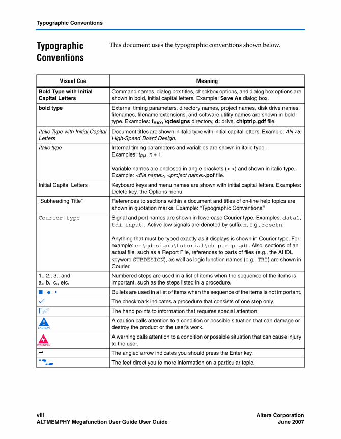
Typographic Conventions
Typographic Conventions
This document uses the typographic conventions shown below.
Visual Cue Meaning
Bold Type with Initial Capital Letters
Command names, dialog box titles, checkbox options, and dialog box options are shown in bold, initial capital letters. Example: Save As dialog box.
bold type External timing parameters, directory names, project names, disk drive names, filenames, filename extensions, and software utility names are shown in bold type. Examples: fMAX, \qdesigns directory, d: drive, chiptrip.gdf file.
Italic Type with Initial Capital Letters
Document titles are shown in italic type with initial capital letters. Example: AN 75: High-Speed Board Design.
Italic type Internal timing parameters and variables are shown in italic type. Examples: tPIA, n + 1.
Variable names are enclosed in angle brackets (< >) and shown in italic type. Example: <file name>, <project name>.pof file.
Initial Capital Letters Keyboard keys and menu names are shown with initial capital letters. Examples: Delete key, the Options menu.
“Subheading Title” References to sections within a document and titles of on-line help topics are shown in quotation marks. Example: “Typographic Conventions.”
Courier type Signal and port names are shown in lowercase Courier type. Examples: data1, tdi, input. Active-low signals are denoted by suffix n, e.g., resetn.
Anything that must be typed exactly as it displays is shown in Courier type. For example: c:\qdesigns\tutorial\chiptrip.gdf. Also, sections of an actual file, such as a Report File, references to parts of files (e.g., the AHDL keyword SUBDESIGN), as well as logic function names (e.g., TRI) are shown in Courier.
1., 2., 3., anda., b., c., etc.
Numbered steps are used in a list of items when the sequence of the items is important, such as the steps listed in a procedure.
■ ● • Bullets are used in a list of items when the sequence of the items is not important.
v The checkmark indicates a procedure that consists of one step only.
1 The hand points to information that requires special attention.
c A caution calls attention to a condition or possible situation that can damage or destroy the product or the user’s work.
w A warning calls attention to a condition or possible situation that can cause injury to the user.
r The angled arrow indicates you should press the Enter key.
f The feet direct you to more information on a particular topic.

Altera Corporation 1–1June 2007 ALTMEMPHY Megafunction User Guide
Chapter 1. About thisMegafunction
Device Family Support
Megafunctions provide either full or preliminary support for target Altera® device families, as described below:
■ Full support means the megafunction meets all functional and timing requirements for the device family and may be used in production designs.
■ Preliminary support means the megafunction meets all functional requirements, but may still be undergoing timing analysis for the device family.
Tables 1–1 and 1–2 show the level of support offered by the ALTMEMPHY megafunction for each Altera device family.
Table 1–1. Half-Rate and Full-Rate Support
Device Family Half Rate Full Rate
Stratix® III v No
Cyclone® III v vStratix II/Stratix II GX v vHardCopy® II v vArria™ GX v v
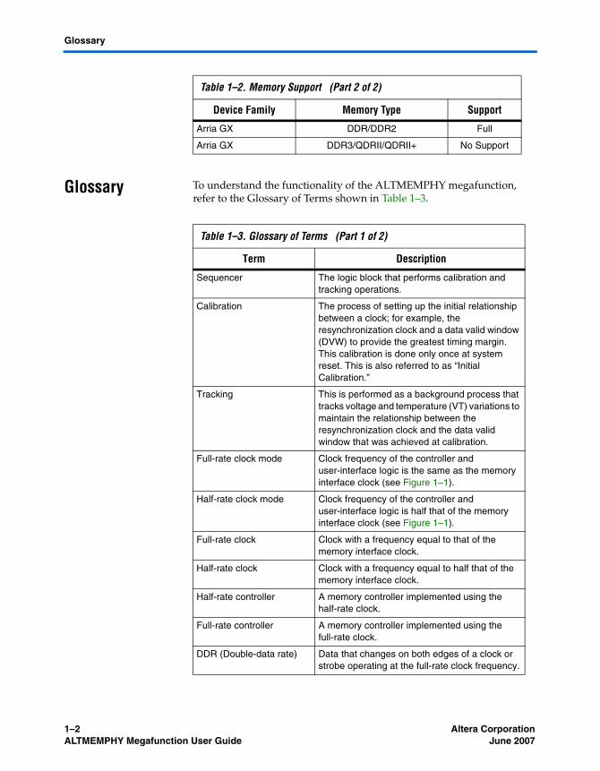
Table 1–2. Memory Support (Part 1 of 2)
Device Family Memory Type Support
Stratix III DDR/DDR2/DDR3/QDRII/QDRII+ Preliminary
Cyclone III DDR/DDR2 Preliminary
Cyclone III DDR3/QDRII/QDRII+ No Support
Stratix II/Stratix II GX DDR/DDR2 Full
Stratix II/Stratix II GX DDR3/QDRII/QDRII+ No Support
HardCopy II DDR/DDR2 Preliminary
1–2 Altera CorporationALTMEMPHY Megafunction User Guide June 2007
Glossary
Glossary To understand the functionality of the ALTMEMPHY megafunction, refer to the Glossary of Terms shown in Table 1–3.
Arria GX DDR/DDR2 Full
Arria GX DDR3/QDRII/QDRII+ No Support
Table 1–2. Memory Support (Part 2 of 2)
Device Family Memory Type Support
Table 1–3. Glossary of Terms (Part 1 of 2)
Term Description
Sequencer The logic block that performs calibration and tracking operations.
Calibration The process of setting up the initial relationship between a clock; for example, the resynchronization clock and a data valid window (DVW) to provide the greatest timing margin. This calibration is done only once at system reset. This is also referred to as “Initial Calibration.”
Tracking This is performed as a background process that tracks voltage and temperature (VT) variations to maintain the relationship between the resynchronization clock and the data valid window that was achieved at calibration.
Full-rate clock mode Clock frequency of the controller and user-interface logic is the same as the memory interface clock (see Figure 1–1).
Half-rate clock mode Clock frequency of the controller and user-interface logic is half that of the memory interface clock (see Figure 1–1).
Full-rate clock Clock with a frequency equal to that of the memory interface clock.
Half-rate clock Clock with a frequency equal to half that of the memory interface clock.
Half-rate controller A memory controller implemented using the half-rate clock.
Full-rate controller A memory controller implemented using the full-rate clock.
DDR (Double-data rate) Data that changes on both edges of a clock or strobe operating at the full-rate clock frequency.

Altera Corporation 1–3June 2007 ALTMEMPHY Megafunction User Guide
About this Megafunction
Figure 1–1 shows the differences in the datapath width and the frequency at which the data is handled between full-rate and half-rate controllers.
Figure 1–1. Full-Rate and Half-Rate Controller Description
Introduction Altera’s ALTMEMPHY megafunction allows the rapid creation of a physical layer interface (PHY) in Stratix II/Stratix II GX, Stratix III, Cyclone III, HardCopy II, and Arria GX devices. The PHY safely transfers data between memory and user logic. The easy-to-use ALTMEMPHY megafunction GUI enables the rapid configuration of the highly configurable PHY. The ALTMEMPHY megafunction can be used with either a user-designed controller or with the Altera DDR and DDR2 SDRAM high-performance controllers. The ALTMEMPHY megafunction can be configured either to support a full-rate or a half-rate controller.
The major advantage of the new ALTMEMPHY megafunction is that it supports an initial calibration sequence to remove process variations in the FPGA and memory device. During operation, the voltage and
SDR (Single-data rate) Data that changes on one edge of the full-rate clock (twice the width of DDR data).
HDR (Half-data rate) Data that changes on one edge of the half-rate clock (twice the width of SDR data and four times the width of DDR data).
Legacy core The integrated PHY and controller core with no support for calibration and tracking (for example, DDR and DDR2 SDRAM Controller Compiler function).
Table 1–3. Glossary of Terms (Part 2 of 2)
Term Description
8 16DDRto SDR User
Logic
FPGA
8 16DDRto SDR User
Logic
FPGA
Full Rate(As used in the legacy core and full rate ALTMEMPHY)
Half Rate(As used in the new ALTMEMPHY)
SDR to HDR
32
Mem
ory
Mem
ory
DDR SDRDDR200 MHz
SDR200 MHz
200 MHz 100 MHz200 MHzHDR
1–4 Altera CorporationALTMEMPHY Megafunction User Guide June 2007
Introduction
temperature (VT) tracking mechanism eliminates the effects on timing margin of VT variation. The calibration process centers the resynchronization clock phase into the middle of the data valid window to maximize the setup and hold margin.
1 Go to http://www.altera.com/literature/tb/tb-091.pdf for selection criteria such as whether to use the legacy DDR/DDR2 SDRAM controller or the DDR/DDR2 SDRAM High-Performance Controller with the ALTMEMPHY megafunction.
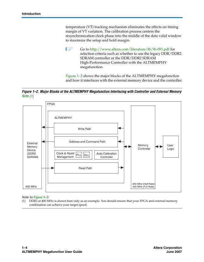
Figure 1–2 shows the major blocks of the ALTMEMPHY megafunction and how it interfaces with the external memory device and the controller.
Figure 1–2. Major Blocks of the ALTMEMPHY Megafunction Interfacing with Controller and External Memory Note (1)
Note to Figure 1–2:(1) DDR2 at 400 MHz is shown here only as an example. You should ensure that your FPGA and external memory
combination can achieve your target speed.
ExternalMemoryDevice(DDR2SDRAM)
ALTMEMPHY
Write Path
Address and Command Path
Clock & ResetManagement
Auto-CalibrationController
Read Path
MemoryController
UserLogic
400 MHz200 MHz (Half Rate)400 MHz (Full Rate)
PLL
FPGA
DLL

Altera Corporation 1–5June 2007 ALTMEMPHY Megafunction User Guide
About this Megafunction
The ALTMEMPHY megafunction is used as an interface between the memory controller and the memory devices to perform read and write operations to the memory. The megafunction is available as a stand-alone product or as an integrated product with the high-performance memory controllers. As a stand-alone product, you can use ALTMEMPHY with either custom or third-party controllers. The ALTMEMPHY megafunction is composed of the following functional units:
■ Read datapath■ Write datapath■ Address and command datapath■ Clock and reset management■ Auto-calibration controller
A detailed explanation of the functional units is presented in “Specifications” on page 3–1.
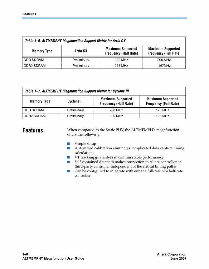
Support Matrix The ALTMEMPHY megafunction support matrices for Stratix III, Stratix II, Stratix II GX, Arria GX, and Cyclone III are shown in Tables 1–4 through 1–7.
1 The performance numbers correspond to the highest speed grade of the device family.
Table 1–4. ALTMEMPHY Megafunction Support Matrix for Stratix III
Memory Type Stratix III Maximum Supported Frequency (Half Rate)
Maximum Supported Frequency (Full Rate)
DDR SDRAM Preliminary 200 MHz No Support
DDR2 SDRAM Preliminary 400 MHz No Support
DDR3 SDRAM Preliminary 400 MHz No Support
QDRII/QDRII+ Preliminary 350 MHz No Support
Table 1–5. ALTMEMPHY Megafunction Support Matrix for Stratix II and Stratix II GX
Memory Type Stratix IIStratix II GX
Maximum Supported Frequency (Half Rate)
Maximum Supported Frequency (Full Rate)
DDR SDRAM Full 200 MHz 200 MHz
DDR2 SDRAM Full 333 MHz 233 MHz
1–6 Altera CorporationALTMEMPHY Megafunction User Guide June 2007
Features
Features When compared to the Static PHY, the ALTMEMPHY megafunction offers the following:
■ Simple setup■ Automated calibration eliminates complicated data capture timing
calculations■ VT tracking guarantees maximum stable performance■ Self-contained datapath makes connection to Altera controller or
third-party controller independent of the critical timing paths■ Can be configured to integrate with either a full-rate or a half-rate
controller
Table 1–6. ALTMEMPHY Megafunction Support Matrix for Arria GX
Memory Type Arria GX Maximum Supported Frequency (Half Rate)
Maximum Supported Frequency (Full Rate)
DDR SDRAM Preliminary 200 MHz 200 MHz
DDR2 SDRAM Preliminary 233 MHz 167MHz
Table 1–7. ALTMEMPHY Megafunction Support Matrix for Cyclone III
Memory Type Cyclone III Maximum Supported Frequency (Half Rate)
Maximum Supported Frequency (Full Rate)
DDR SDRAM Preliminary 200 MHz 125 MHz
DDR2 SDRAM Preliminary 200 MHz 125 MHz
Altera Corporation 1–7June 2007 ALTMEMPHY Megafunction User Guide
About this Megafunction
Resource Utilization and Performance
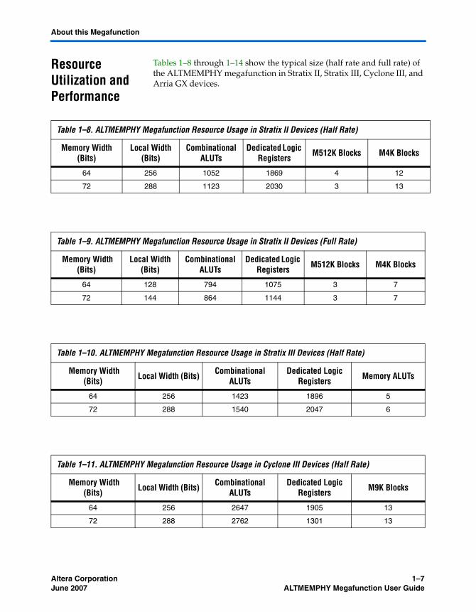
Tables 1–8 through 1–14 show the typical size (half rate and full rate) of the ALTMEMPHY megafunction in Stratix II, Stratix III, Cyclone III, and Arria GX devices.
Table 1–8. ALTMEMPHY Megafunction Resource Usage in Stratix II Devices (Half Rate)
Memory Width(Bits)
Local Width (Bits)
Combinational ALUTs
Dedicated Logic Registers M512K Blocks M4K Blocks
64 256 1052 1869 4 12
72 288 1123 2030 3 13
Table 1–9. ALTMEMPHY Megafunction Resource Usage in Stratix II Devices (Full Rate)
Memory Width(Bits)
Local Width (Bits)
Combinational ALUTs
Dedicated Logic Registers M512K Blocks M4K Blocks
64 128 794 1075 3 7
72 144 864 1144 3 7
Table 1–10. ALTMEMPHY Megafunction Resource Usage in Stratix III Devices (Half Rate)
Memory Width(Bits) Local Width (Bits) Combinational
ALUTsDedicated Logic
Registers Memory ALUTs
64 256 1423 1896 5
72 288 1540 2047 6
Table 1–11. ALTMEMPHY Megafunction Resource Usage in Cyclone III Devices (Half Rate)
Memory Width(Bits) Local Width (Bits) Combinational
ALUTsDedicated Logic
Registers M9K Blocks
64 256 2647 1905 13
72 288 2762 1301 13

1–8 Altera CorporationALTMEMPHY Megafunction User Guide June 2007
Resource Utilization and Performance
Table 1–12. ALTMEMPHY Megafunction Resource Usage in Cyclone III Devices (Full Rate)
Memory Width(Bits) Local Width (Bits) Combinational
ALUTsDedicated Logic
Registers M9K Blocks
64 128 1664 1123 7
72 144 1782 1209 7
Table 1–13. ALTMEMPHY Megafunction Resource Usage in Arria GX Devices (Half Rate)
Memory Width(Bits)
Local Width (Bits)
Combinational ALUTs
Dedicated Logic Registers M512K Blocks M4K Blocks
64 256 1122 1883 4 12
72 288 1193 2044 3 13
Table 1–14. ALTMEMPHY Megafunction Resource Usage in Arria GX Devices (Full Rate)
Memory Width(Bits)
Local Width (Bits)
Combinational ALUTs
Dedicated Logic Registers M512K Blocks M4K Blocks
64 128 855 1088 4 12
72 144 901 1164 3 13
Altera Corporation 2–1June 2007 ALTMEMPHY Megafunction User Guide
Chapter 2. Getting Started
System Requirements
The instructions in this section require the following hardware and software:
■ For OS Support information, refer to:
http://www.altera.com/support/software/os_support/oss-index.html
■ The Quartus® II software version 7.1 or higher
MegaWizard Plug-In Manager Customization
Use the MegaWizard® Plug-In Manager to specify the ALTMEMPHY megafunction in your design. Start the MegaWizard Plug-In Manager in one of the following ways:
■ On the Tools menu, click MegaWizard Plug-In Manager.■ When working in the Block Editor, click MegaWizard Plug-In
Manager in the Symbol dialog box. ■ Start the stand-alone version of the MegaWizard Plug-In Manager by
typing the following command at the command prompt: qmegawiz.
1 The ALTMEMPHY megafunction is also instantiated when the high-performance controller is generated using the MegaWizard Plug-In Manager. There is no need to launch the ALTMEMPHY MegaWizard Plug-In Manager separately. Refer to “Compiling in the Quartus II Software” on page 2–16 for more details.
1 Refer to Quartus II Help for more information on how to use the MegaWizard Plug-In Manager.
MegaWizard Page Descriptions
This section provides descriptions of the options available on the ALTMEMPHY MegaWizard Plug-In Manager pages.

2–2 Altera CorporationALTMEMPHY Megafunction User Guide June 2007
MegaWizard Page Descriptions
On page 1 of the MegaWizard Plug-In Manager, select Create a new custom megafunction variation from the three available options shown in Figure 2–1 and click Next.
Figure 2–1. MegaWizard Plug-In Manager [page 1]
On page 2a of the MegaWizard Plug-In Manager, select ALTMEMPHY by expanding the I/O section in the Megafunction list. Select the appropriate device family, output file type, and name of your output file.
Figure 2–2 shows an example of an ALTMEMPHY megafunction named phy.v.
1 The <variation name> must be a different name from the project name and the top-level design entity name.

Altera Corporation 2–3June 2007 ALTMEMPHY Megafunction User Guide
Getting Started
Figure 2–2. MegaWizard Plug-In Manager [page 2a]
Click Next to launch the ALTMEMPHY Parameter Settings page (Figure 2–3).
Figure 2–3 shows the ALTMEMPHY Parameter Settings page. By clicking on the appropriate tab, this page allows you to parameterize:
■ Memory settings■ PHY settings
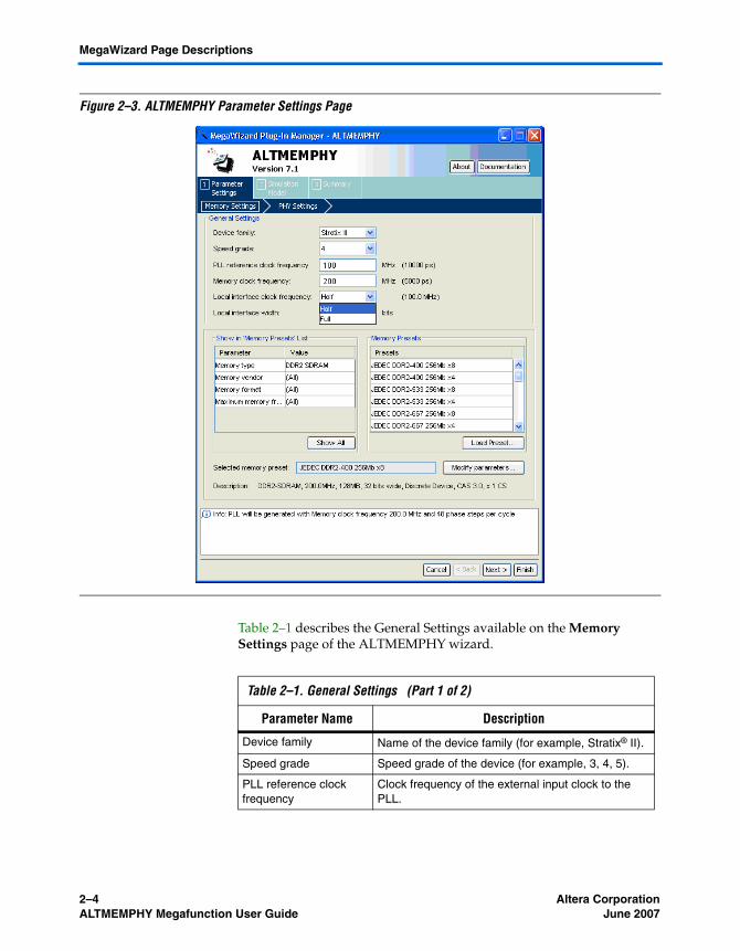
2–4 Altera CorporationALTMEMPHY Megafunction User Guide June 2007
MegaWizard Page Descriptions
Figure 2–3. ALTMEMPHY Parameter Settings Page
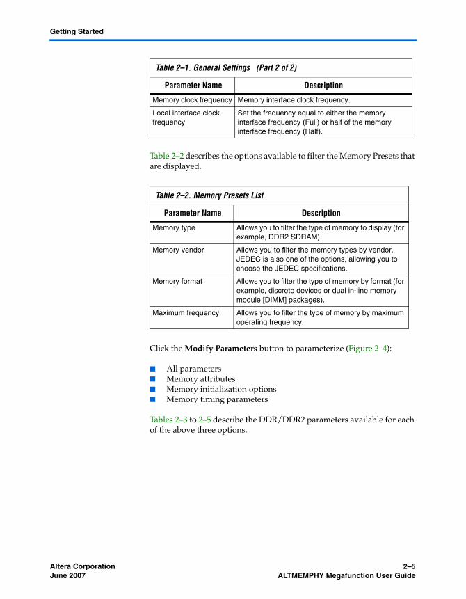
Table 2–1 describes the General Settings available on the Memory Settings page of the ALTMEMPHY wizard.
Table 2–1. General Settings (Part 1 of 2)
Parameter Name Description
Device family Name of the device family (for example, Stratix® II).
Speed grade Speed grade of the device (for example, 3, 4, 5).
PLL reference clock frequency
Clock frequency of the external input clock to the PLL.
Altera Corporation 2–5June 2007 ALTMEMPHY Megafunction User Guide
Getting Started
Table 2–2 describes the options available to filter the Memory Presets that are displayed.
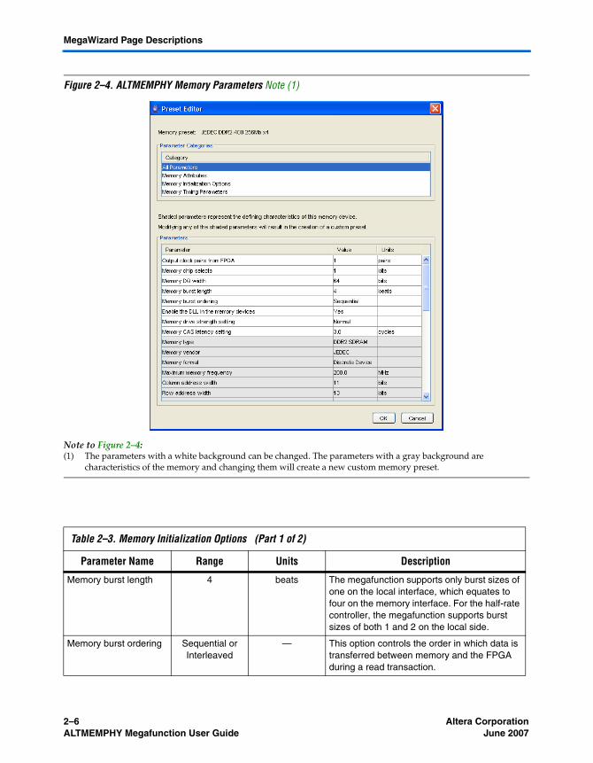
Click the Modify Parameters button to parameterize (Figure 2–4):
■ All parameters■ Memory attributes■ Memory initialization options ■ Memory timing parameters
Tables 2–3 to 2–5 describe the DDR/DDR2 parameters available for each of the above three options.
Memory clock frequency Memory interface clock frequency.
Local interface clock frequency
Set the frequency equal to either the memory interface frequency (Full) or half of the memory interface frequency (Half).
Table 2–2. Memory Presets List
Parameter Name Description
Memory type Allows you to filter the type of memory to display (for example, DDR2 SDRAM).
Memory vendor Allows you to filter the memory types by vendor. JEDEC is also one of the options, allowing you to choose the JEDEC specifications.
Memory format Allows you to filter the type of memory by format (for example, discrete devices or dual in-line memory module [DIMM] packages).
Maximum frequency Allows you to filter the type of memory by maximum operating frequency.
Table 2–1. General Settings (Part 2 of 2)
Parameter Name Description
2–6 Altera CorporationALTMEMPHY Megafunction User Guide June 2007
MegaWizard Page Descriptions
Figure 2–4. ALTMEMPHY Memory Parameters Note (1)
Note to Figure 2–4:(1) The parameters with a white background can be changed. The parameters with a gray background are
characteristics of the memory and changing them will create a new custom memory preset.
Table 2–3. Memory Initialization Options (Part 1 of 2)
Parameter Name Range Units Description
Memory burst length 4 beats The megafunction supports only burst sizes of one on the local interface, which equates to four on the memory interface. For the half-rate controller, the megafunction supports burst sizes of both 1 and 2 on the local side.
Memory burst ordering Sequential or Interleaved
— This option controls the order in which data is transferred between memory and the FPGA during a read transaction.
Altera Corporation 2–7June 2007 ALTMEMPHY Megafunction User Guide
Getting Started
Enable the DLL in the memory devices
On or Off — When turned on, the DLL within the memory device is enabled. The default option is yes.
Memory drive strength setting
Normal or Reduced
— Controls the drive strength of the memory device’s output buffers. Reduced drive strength is not supported on all memory devices. The default option is normal.
Memory CAS latency setting
2.0, 2.5, 3.0, 4.0, 5.0, 6.0, 7.0
Cycles The delay in clock cycles from the read command to the first output data from the memory.
Memory latency setting 1.5 for DQRII and 2.0, 2.5 for
QDRII+
Cycles Defines the memory read latency.
Table 2–3. Memory Initialization Options (Part 2 of 2)
Parameter Name Range Units Description
Table 2–4. Memory Attributes Settings (Part 1 of 2)
Parameter Name Range (1) Units Description
Memory vendor – – Name of the memory vendor.
Maximum frequency supported by memory
See the memory device datasheet
MHz Maximum frequency supported by the memory.
Column address width 8–13 bits The number of column address bits for your memory.
Row address width 10–14 bits The number of row address bits for your memory.
Bank address width 2 or 3 bits The number of bank address bits for your memory.
Output clock pairs from FPGA
1–6 integer The number of differential clock pairs driven from the FPGA to the memory. More clock pairs reduce the loading of each output.
Chip selects per DIMM 1–8 – The number of chip selects on each DIMM in your memory system.
DQ bits per DQS bit 4 or 8 bits The number of data (DQ) bits for each data strobe (DQS) pin.
Precharge all address bit 8 or 10 – The bit of the address bus to use as the precharge “all” address bit.
Memory chip selects 1, 2, 4, or 8 – The number of chip selects in your memory interface. This is the depth of your memory in terms of number of chips.

2–8 Altera CorporationALTMEMPHY Megafunction User Guide June 2007
MegaWizard Page Descriptions
Memory DQ width ≥ 4 bits Number of DQ pins on the memory interface.
Note to Table 2–4:(1) The range values depend on the memory used.
Table 2–5. Memory Timing Parameter Settings Note (1) (Part 1 of 2)
Parameter Name Range Units Description
(tINT) 0.001–1000
μs Minimum memory initialization time. After reset, the controller does not issue any commands to the memory during this period.
(tMRD) 2–39 ns Minimum load mode register command period. The controller waits for this period of time after issuing a load mode register command before issuing any other commands.
(tRAS) 8–200 ns Minimum active to precharge time. The controller waits for this period of time after issuing an active command before issuing a precharge command to the same bank.
(tRCD) 4–65 ns Minimum active to read-write time. The controller does not issue read or write commands to a bank during this period of time after issuing an active command.
(tRP) 4–65 ns Minimum precharge command period. The controller does not access the bank for this period of time after issuing a precharge command.
(tREFI) 1–65534 μs Maximum interval between refresh commands. The controller performs regular refresh at this interval unless user-controlled refresh is turned on.
(tRFC) 14–1651 ns Minimum auto-refresh command period. The length of time the controller waits before doing anything else after issuing an auto-refresh command.
(tWR) 4–65 ns Minimum write recovery time. The controller waits for this period of time after the end of a write transaction before issuing a precharge command.
(tWTR) 2–39 tCK Minimum write-to-read command delay. The controller waits for this period of time after the end of a write command before issuing a subsequent read command to the same bank. This timing parameter is specified in clock cycles and the value is rounded off to the next integer.
(tAC) 300–750 ps DQ output access time.
(tDHA) 10–600 ps DQ and DM input hold time relative to DQS.
(tDQSQ) 100–500 ps The maximum DQS to DQ skew; DQS to last DQ valid, per group, per access.
Table 2–4. Memory Attributes Settings (Part 2 of 2)
Parameter Name Range (1) Units Description
Altera Corporation 2–9June 2007 ALTMEMPHY Megafunction User Guide
Getting Started
Tables 2–6 to 2–8 describe the QDRII/QDRII+ SRAM parameters available for each of the following three options.
■ Memory initialization options■ Memory attribute settings■ Memory timing parameter settings
(tDQSS) 0–0.3 tCK Positive DQS latching edge to associated clock edge (tCK).
(tDSA) 10–600 ps DQ and DM input setup time relative to DQS (ps).
(tDSH) 0.1–0.5 tCK DQS falling edge to CK rising - hold time (tCK).
(tDSS) 0.1–0.5 tCK DQS falling edge to CK rising - setup time (tCK).
(tIHA) 100–1000 ps Address and control input hold time (ps).
(tISA) 100–1000 ps Address and control input setup time (ps).
(tQHS) 100–700 ps The maximum data hold skew factor.
Note to Table 2–5:(1) See the memory device datasheet for the parameter range.
Table 2–5. Memory Timing Parameter Settings Note (1) (Part 2 of 2)
Parameter Name Range Units Description
Table 2–6. Memory Initialization Options
Parameter Name Range Units Description
Memory burst length 4 beats The megafunction supports only burst sizes of one on the local interface, which equates to four on the memory interface.
Memory latency setting 1.5 Cycles 1.5 for QDRII; 2.0 and 2.5 for QDRII+.
Table 2–7. Memory Attribute Settings (Part 1 of 2)
Parameter Name Range (1) Units Description
Memory vendor — — Name of the memory vendor.
Maximum memory frequency
See the memory device datasheet
MHz Maximum frequency supported by the memory.
Output clock pairs from FPGA
1-16 integer The number of differential clock pairs driven from the FPGA to the memory. More clock pairs reduce the loading of each output.
2–10 Altera CorporationALTMEMPHY Megafunction User Guide June 2007
MegaWizard Page Descriptions
Memory depth expansion
1-2 chips Number of chip selects of memory supported. This option is used for memory depth expansion.
Drive BWS_N/NWS_N from FPGA
No, Yes — Set to YES if logic is required to drive the Write Select inputs of the memory devices.
DQ bits per chip 8, 9, 18, 36 bits Width of D/Q databus on each QDRII chip.
Memory DQ data bits 8-288 bits Width of external meory read and write databus.
Address width 15-25 bits Number of address bits.
I/O Standard 1.8 V for QDRII1.8 V or 1.5 V
HSTL for QSRII+
— I/O standard to be applied to the memory interface pins.
Note to Table 2–7:(1) The range values depend on the memory used.
Table 2–7. Memory Attribute Settings (Part 2 of 2)
Parameter Name Range (1) Units Description
Table 2–8. Memory Timing Parameter Settings
Parameter Name Range Units Description
(tSA) 200-500 ps Address setup time to K clock rise.
(tSC) 200-500 ps Control setup time to K clock rise.
(tHA) 200-500 ps Address hold time to K clock rise.
(tHC) 200-500 ps Control hold time after K clock rise.
(tSD) 200-500 ps D setup time to K clock rise.
(tHD) 200-500 ps D hold time to K clock rise.
(tCOHQV) 200-500 ps Echo clock high to data valid.
(tCOHOX) 200-500 ps Echo clock high to data invalid.
Altera Corporation 2–11June 2007 ALTMEMPHY Megafunction User Guide
Getting Started
PHY Settings
Click the PHY Settings tab (Figure 2–5) to set the options described in Table 2–9.
Figure 2–5. ALTMEMPHY PHY Parameter Settings Page
Table 2–9. ALTMEMPHY PHY Settings (Part 1 of 2)
Parameter Name Description
Use dedicated PLL outputs to drive memory clocks
Turn on to use dedicated PLL outputs to generate the clocks, which is recommended for HardCopy II devices. When turned off, the ALTDDIO megafunction outputs generate the clock outputs.
Use differential DQS Enable this feature for better signal integrity. This is applicable to Stratix III devices only.
2–12 Altera CorporationALTMEMPHY Megafunction User Guide June 2007
MegaWizard Page Descriptions
Click Next or click the Simulation Model tab (Figure 2–6) to set your Simulation Model settings.
Enable external access to reconfigure PLL prior to calibration
By enabling this option, the inputs to the ALTPLL_RECONFIG is brought to the top level. This option is applicable for HardCopy II devices only. (1)
Instantiate DLL externally
This option allows the DLL to be shared between multiple PHY instances. Enabling this option allows the DLL to be connected externally to the ALTMEMPHY megafunction. (2)
Enable dynamic parallel on-chip termination
This option provides I/O impedance matching and termination capabilities. This is applicable for Stratix III devices and is used for bidirectional signals such as DQ and DQS.
Clock phase Adjusting the address and command phase can improve the address and command setup and hold margins at the memory device to compensate for the propagation delays that vary with different loadings. Applicable to Stratix III and Cyclone III devices. (3)
Dedicated clock phase Only applicable to Stratix III devices and should be left to default settings for the Quartus II software version 7.1.
Board skew The worst case board delay skew between clock DQS and its respective DQ pins (in ps).
Calibrate using a single DQ pin only to reduce simulation time (recommended)
Calibration of the resynchronization clock is done using the data read through one DQ pin. This reduces simulation time. (4)
Calibrate using all DQ pins to match the hardware behavior exactly (will result in much longer simulation time)
Calibration of the resynchronization clock is done using the data read through DQ pins one after another. This results in increased simulation time. (4)
Notes to Table 2–9:(1) Refer to “ALTPLL_RECONFIG” on page 3–9 for more information regarding
this option.(2) Available for the Stratix II device family only.(3) Available for the Stratix III and cyclone III device families only.(4) This option only affects RTL simulation and not the actual hardware or
gate-level simulation.
Table 2–9. ALTMEMPHY PHY Settings (Part 2 of 2)
Parameter Name Description

Altera Corporation 2–13June 2007 ALTMEMPHY Megafunction User Guide
Getting Started
Simulation Model
An IP functional simulation model is a cycle-accurate VHDL or Verilog HDL model produced by the Quartus II software (Figure 2–6). The model allows for fast-functional simulation of IP using industry-standard VHDL and Verilog HDL simulators.
1 You should generate your simulation model in the same language that you are using to generate your megafunction variation. The simulation model that is generated is <project_dir>\<variation>_alt_mem_phy_sequencer_wrapper.vo/.vho, and is used during the RTL Nativelink simulation. Refer to “Simulating ALTMEMPHY” on page 2–22 for more information.
Use these simulation model output files for simulation only. Using these files for synthesis creates a nonfunctional design.

2–14 Altera CorporationALTMEMPHY Megafunction User Guide June 2007
MegaWizard Page Descriptions
Figure 2–6. ALTMEMPHY Simulation Model Generation Page
Click Next to go to the Summary page or click the Summary tab (Figure 2–7).
Summary Page
On the Summary page (Figure 2–7) of the MegaWizard Plug-In Manager, specify the files you wish to have generated for your custom megafunction. The gray check marks indicate files that are always generated; the other files are optional and are generated only if selected (indicated by a black check mark). Choose from:
■ HDL wrapper file, (<variation_name>.v/<variation_name>.vhd)■ Block Symbol file (.bsf)■ VHDL Component declaration file (<variation_name>.cmp) ■ Verilog Black Box declaration file (<variation_name>_bb.v).■ Megafunction report file (<variation_name>.html).
Altera Corporation 2–15June 2007 ALTMEMPHY Megafunction User Guide
Getting Started
Figure 2–7. ALTMEMPHY Summary Page
Inferring Megafunctions from HDL Code
The ALTMEMPHY megafunction cannot be inferred from the HDL code.
Instantiating Megafunctions in HDL Code
When you use the MegaWizard Plug-In Manager to set up and parameterize a megafunction, it creates either a VHDL or Verilog HDL wrapper file that instantiates the megafunction (a black box methodology). Refer to the following for details about how to instantiate a megafunction in your design:
■ Recommended HDL Coding Styles chapter in volume 1 of the Quartus II Handbook.
■ Quartus II Integrated Synthesis chapter in volume 1 of the Quartus II Handbook.

2–16 Altera CorporationALTMEMPHY Megafunction User Guide June 2007
Compiling in the Quartus II Software
■ Synplicity Synplify and Synplify Pro Support chapter in volume 1 of the Quartus II Handbook.
■ Mentor Graphics Precision RTL Synthesis Support chapter in volume 1 of the Quartus II Handbook.
Compiling in the Quartus II Software
ALTMEMPHY can be compiled as a stand-alone top-level design. The advantage of doing this is that you do not have to create a complete design to check that ALTMEMPHY meets your required target frequency. However, this is only a guide and for a more accurate result, you should use a realistic design. A typical scenario of compiling ALTMEMPHY is either when it is integrated with your own controller or when it is integrated with Altera’s DDR/DDR2 SDRAM High-Performance Controller (Figure 2–8).
When using Altera’s DDR and DDR2 SDRAM High-Performance Controller, the controller MegaWizard Plug-In Manager generates both ALTMEMPHY and the High-Performance Memory Controller; there is no need to launch the ALTMEMPHY MegaWizard Plug-In Manager separately. The controller MegaWizard Plug-In Manager also generates an example design consisting of:
■ ALTMEMPHY■ High-performance memory controller ■ Example driver
Each example design can be synthesized and simulated.
Figure 2–8. DDR SDRAM Controller System-Level Diagram
DDR SDRAM
DDR SDRAMInterface
ControlLogic(Encrypted)
DDR SDRAMHigh-PerformanceController
LocalInterface
Example DriverPass or Fail
Example Design
ALTMEMPHY Megafunction

Altera Corporation 2–17June 2007 ALTMEMPHY Megafunction User Guide
Getting Started
Perform the following steps before you compile the design:
1. Enable the TimeQuest timing analyzer (Figure 2–9) by selecting the following:
a. On the Assignments menu, click Settings, expand Timing Analysis Settings, and select Use TimeQuest Timing Analyzer during compilation and click OK.
b. Add the Synopsys design constraints file, <variation name>_phy_ddr_timing.sdc, to your project. On the Project menu, click Add/Remove Files in Project and browse the file.
Figure 2–9. Enabling the TimeQuest Timing Analyzer
2. Add pin I/O standard assignments in one of the following ways:
1 The I/O standard pin assignment script is not run automatically. As a result, all pins may likely have the wrong I/O standard assigned causing the Quartus II fitter to fail. Therefore, you must run the I/O standard assignment script manually before running the Quartus II fitter.
a. For Stratix III devices, you must run <variation name>_pin_assignments.tcl.
2–18 Altera CorporationALTMEMPHY Megafunction User Guide June 2007
Compiling in the Quartus II Software
b. For all other devices, run <variation name>_pin_assignments.tcl.
1 Before running the Tcl scripts, modify the pin names to reflect the pin names in the top-level design.
or follow these steps:
• Edit your top-level design to add a prefix to all DDR or DDR2 signal names. For example, change mem_ddr to core1_mem_addr.
• On the Assignments menu, click Pins. Right-click in the window and click Create/Import Megafunction. Select Import an existing custom megafunction and navigate to <variation name>.ppf.
• Type the prefix that you added to your top-level DDR or DDR2 signal names into the Instance name box and click OK.
3. Set the top-level entity to the example project.
a. On the File menu, click Open.
b. Browse to <variation name>_example_top.v/.vhd created by the DDR/DDR2 High Performance Controller megafunction or your top-level design file and click Open.
c. On the Project menu, click Set as top-level entity.
4. On the Processing menu, point to Start and click Start Analysis and Synthesis.
5. Assign the DQ and DQS pin groups.
a. For Stratix III devices only, add the DQ group assignments to relate the DQ and DQS pin groups together for the Quartus II fitter to place them correctly, by running <variation name>_assign_dq_groups.tcl.
1 Before running the Tcl scripts, modify the pin names to reflect the pin names in the top level design.
1 For all other families, the following steps are optional.
b. Manually specify all DQ and DQS pins to align your project with your PCB requirements.

Altera Corporation 2–19June 2007 ALTMEMPHY Megafunction User Guide
Getting Started
or
c. Manually specify all other project pin locations to align your project with your PCB requirements.
1 When you are assigning pins, ensure the I/O standard is set to one compatible with your memory device and compatible with the other pins sharing the I/O bank. For example, for the clock source, the reset, and the address and command signals. Also, select which bank or side of the device you want the Quartus II software to place them in.
6. Set the output pin loading for all memory interface pins.
7. Select your required I/O driver strength (derived from simulation) to ensure that you correctly drive each signal and do not suffer from overshoot or undershoot.
8. On the Process menu, click Start Compilation to compile the design.
9. Optional: Run a report timing to get a detailed DDR SDRAM interface timing report. Run <variation name>_report_timing.tcl:
a. On the Tools menu, click Tcl scripts.
or
b. On the Tools menu, click TimeQuest Timing Analyzer. Go to the left pane and double-click Read SDC File, then on the Script menu, select <variation name>_report_timing.tcl.
f To attach the SignalTap II logic analyzer to your design, refer to AN 380: Test DDR or DDR2 SDRAM Interfaces on Hardware Using the Example Driver.
Analyzing Timing
Timing analysis of the ALTMEMPHY megafunction is critical if your hardware is to operate as intended. Timing analysis scripts that are generated along with ALTMEMPHY enable you to perform detailed timing analysis of both core and I/O timing paths, as shown in Table 2–10. Timing analysis of ALTMEMPHY is supported by the TimeQuest static timing analyzer only, for the following reasons:
■ The timing constraints scripts generated along with the ALTMEMPHY megafunction supports only the TimeQuest static timing analyzer.
2–20 Altera CorporationALTMEMPHY Megafunction User Guide June 2007
Analyzing Timing
■ The Classic Timing Analyzer (TAN) does not offer analysis of source-synchronous outputs; for example, write data, and address and command outputs.
f For more information about Timing Analysis, refer to AN 438: Constraining and Analyzing Timing for External Memory Interfaces.
Timing Constraints
The MegaWizard Plug-In Manager-generated SDC script file <variation_name>_ddr_timing.sdc, found in the project directory, sets the following constraints on the ALTMEMPHY megafunction:
■ Creates all the necessary clocks with proper clock periods■ Sets all the board and memory parameter settings ■ Sets the output delay on the DQS pins for write analysis■ Sets the input delay on the DQS pins for read analysis■ Sets clock uncertainty for DQS pins versus CK pins timing analysis■ Sets the output delay on the address and command pins■ Sets necessary multicycle path assignments
Timing Analysis Using the TimeQuest Timing Analyzer
This section describes the steps required to perform timing analysis of the ALTMEMPHY megafunction.
1. Generate the ALTMEMPHY megafunction with the desired parameter settings as explained in “MegaWizard Plug-In Manager Customization” on page 2–1.
2. Perform the preliminary steps as described in “Compiling in the Quartus II Software” on page 2–16.
3. Compile the design.
4. Perform timing analysis. To see the timing report, you can either:
● Execute the Tcl script with the Quartus II software (by choosing Tools -> Tcl scripts -> <variation_name>_report_timing.tcl) or
● Run the timing analysis inside the TimeQuest timing analyzer by choosing Tools -> TimeQuest Timing Analyzer
Inside the TimeQuest tool, double-click on Update Timing Netlist to load your design and analyze it. You can now report timing paths by the TimeQuest methods as described in “Timing Analysis Using the TimeQuest Timing Analyzer” on page 2–20, or run the Tcl script
Altera Corporation 2–21June 2007 ALTMEMPHY Megafunction User Guide
Getting Started
<project_dir>/<variation_name>_report_timing.tcl by choosing Tools -> Tcl scripts, which creates a set of pre-defined reports for the critical paths (refer to Table 2–10).
1 Timing analysis of ALTMEMPHY confirms that the ALTMEMPHY megafunction can operate at the desired frequency. The <project_dir>/<variation_name>_ddr_timing.sdc script can be used when the top-level design is either ALTMEMPHY alone or when ALTMEMPHY is used along with the controller and user logic.
Timing Paths
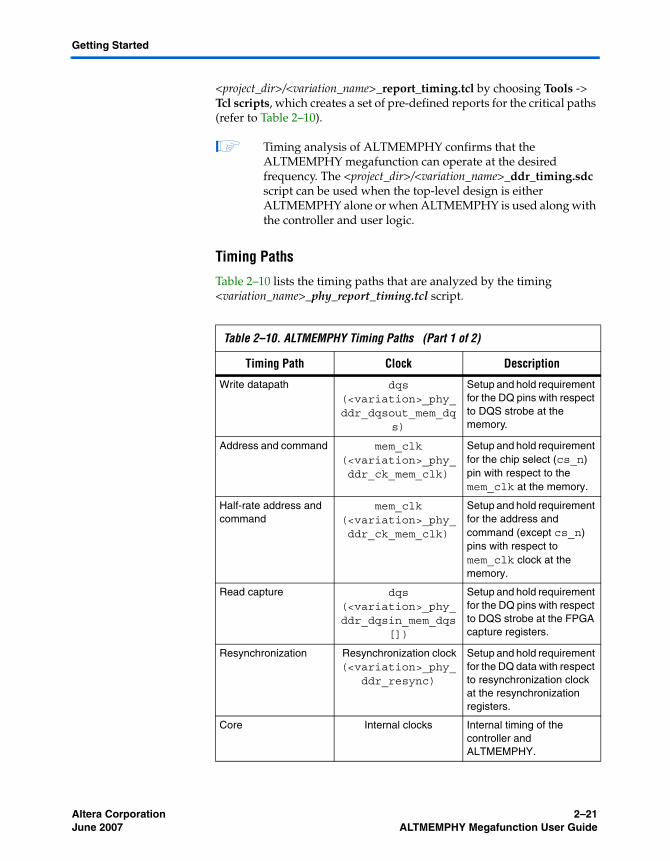
Table 2–10 lists the timing paths that are analyzed by the timing <variation_name>_phy_report_timing.tcl script.
Table 2–10. ALTMEMPHY Timing Paths (Part 1 of 2)
Timing Path Clock Description
Write datapath dqs (<variation>_phy_ddr_dqsout_mem_dq
s)
Setup and hold requirement for the DQ pins with respect to DQS strobe at the memory.
Address and command mem_clk (<variation>_phy_ddr_ck_mem_clk)
Setup and hold requirement for the chip select (cs_n) pin with respect to the mem_clk at the memory.
Half-rate address and command
mem_clk (<variation>_phy_ddr_ck_mem_clk)
Setup and hold requirement for the address and command (except cs_n) pins with respect to mem_clk clock at the memory.
Read capture dqs (<variation>_phy_ddr_dqsin_mem_dqs
[])
Setup and hold requirement for the DQ pins with respect to DQS strobe at the FPGA capture registers.
Resynchronization Resynchronization clock (<variation>_phy_
ddr_resync)
Setup and hold requirement for the DQ data with respect to resynchronization clock at the resynchronization registers.
Core Internal clocks Internal timing of the controller and ALTMEMPHY.

2–22 Altera CorporationALTMEMPHY Megafunction User Guide June 2007
Simulating ALTMEMPHY
f For more information about timing paths analyzed, refer to AN 438: Constraining and Analyzing Timing for External Memory Interfaces.
Simulating ALTMEMPHY
The ALTMEMPHY megafunction cannot be simulated on its own. To simulate the ALTMEMPHY megafunction, you will need the following:
■ Memory controller■ Example driver (to initiate read and write transactions)■ Testbench and a suitable memory model
If you generate the high-performance controller using the MegaWizard Plug-In Manager, it will also generate a testbench that can be simulated using Altera-supported third-party simulators.
Simulation of the ALTMEMPHY megafunction is supported through Nativelink, whether in the context of Altera’s example design or your own design.
1 Refer to the High-Performance Controller User Guide to learn more about simulating the example design that instantiates the ALTMEMPHY megafunction.
Postamble Postamble clock (<variation>_phy_ddr_delayed_dqs)
Setup and hold requirements for the postamble-enable registers with respect to the postamble clock.
Mimic path Measure clock (<variation>_phy_
ddr_mimic)
Placement and routing of the mimic path register with respect to the mem_ck output pins, such that it matches the resynchronization path.
Table 2–10. ALTMEMPHY Timing Paths (Part 2 of 2)
Timing Path Clock Description
Altera Corporation 2–23June 2007 ALTMEMPHY Megafunction User Guide
Getting Started
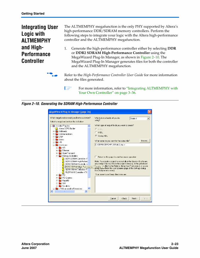
Integrating User Logic with ALTMEMPHY and High- Performance Controller
The ALTMEMPHY megafunction is the only PHY supported by Altera’s high-performance DDR/SDRAM memory controllers. Perform the following steps to integrate your logic with the Altera high-performance controller and the ALTMEMPHY megafunction.
1. Generate the high-performance controller either by selecting DDR or DDR2 SDRAM High-Performance Controller using the MegaWizard Plug-In Manager, as shown in Figure 2–10. The MegaWizard Plug-In Manager generates files for both the controller and the ALTMEMPHY megafunction.
f Refer to the High-Performance Controller User Guide for more information about the files generated.
1 For more information, refer to “Integrating ALTMEMPHY with Your Own Controller” on page 3–36.
Figure 2–10. Generating the SDRAM High-Performance Controller

2–24 Altera CorporationALTMEMPHY Megafunction User Guide June 2007
Integrating User Logic with ALTMEMPHY and High- Performance Controller
The hierarchy of the top-level design generated by the MegaWizard Plug-In Manager is shown in Figure 2–11.
Figure 2–11. Hierarchy of the Top-Level Design
As shown in Figure 2–11, the top-level design instantiates the instance ddr2_top_controller_phy, which in turn instantiates and integrates ALTMEMPHY and the controller.
2. Integrate your driver logic with the controller and ALTMEMPHY.
1 The top-level design generated by the MegaWizard Plug-In Manager has an example driver. Remove that driver and integrate your driver logic.
3. Complete synthesis and simulation.
f For more information about Steps 2 and 3, refer to the High-Performance Controller User Guide.
Top level of DDR2interface
ddr2_top_example_top.v/.vhd
Driver/user logic issuesreads/writes
ddr2_top_example_driver.v/.vhd
Instantiates PHY andcontroller
ddr2_top_controller_phy.v/.vhd
Controller coreddr2_top_auk_ddr_hp_co
ntroller_wrapper.v/.vhd
PHY top levelddr2_top_phy.v/.vhd
Altera Corporation 3–1June 2007 ALTMEMPHY Megafunction User Guide
Chapter 3. Specifications
Stratix II Support for DDR/DDR2 SDRAM
This chapter describes the operation of different blocks of the ALTMEMPHY megafunction based on the supported FPGA families.
The following sections describe the ALTMEMPHY megafunction support for Stratix® II DDR/DDR2 SDRAM.
Half-Rate Support
The following section discusses half-rate support.
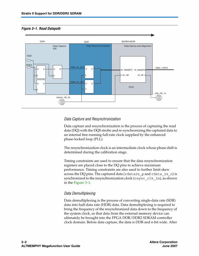
Read Datapath
The read datapath logic is responsible for capturing data sent by the memory device and subsequently aligning the data back to the system clock domain. The functions performed by the read datapath are:
1. Data capture and resynchronization
2. Data demultiplexing
3. Data alignment
Figure 3–1 shows the order of the functions performed by the read datapath, along with the frequency at which the read data is handled.
3–2 Altera CorporationALTMEMPHY Megafunction User Guide June 2007
Stratix II Support for DDR/DDR2 SDRAM
Figure 3–1. Read Datapath
Data Capture and Resynchronization
Data capture and resynchronization is the process of capturing the read data (DQ) with the DQS strobe and re-synchronizing the captured data to an internal free-running full-rate clock supplied by the enhanced phase-locked loop (PLL).
The resynchronization clock is an intermediate clock whose phase shift is determined during the calibration stage.
Timing constraints are used to ensure that the data resynchronization registers are placed close to the DQ pins to achieve maximum performance. Timing constraints are also used to further limit skew across the DQ pins. The captured data (rdata2x_p and rdata_2x_n) is synchronized to the resynchronization clock (rsync_clk_2x), as shown in the Figure 3–1.
Data Demultiplexing
Data demultiplexing is the process of converting single-data rate (SDR) data into half-data rate (HDR) data. Data demultiplexing is required to bring the frequency of the resynchronized data down to the frequency of the system clock, so that data from the external memory device can ultimately be brought into the FPGA DDR/DDR2 SDRAM controller clock domain. Before data capture, the data is DDR and n-bit wide. After
SDRDDR SDR/HDR
D Q D Q
Data CaptureIOE
D Q D Q
D Q
Data Resynchronization Data Demux and Alignment
rdata_1x[4n]wr_data[2n] rd_data[4n]
wr_clk rd_clk
FIFO
phy_clk_1x
rdata_2x_p[n]
rdata_2x_n[n]
resync_clk_2x
DQ[n]
DQS
Altera Corporation 3–3June 2007 ALTMEMPHY Megafunction User Guide
Specifications
data capture, the data is SDR and 2n-bit wide. After data demuxing, the data is HDR of width 4n-bits wide. The system clock frequency is half the frequency of the memory clock.
Demultiplexing is achieved using a dual-port memory with a 2n-bit wide write-port operating on the resynchronization clock (SDR) and a 4n-bit wide read-port operating on the PHY clock (HDR). The basic principle of operation is that data is written to the memory at the SDR rate and read from the memory at the HDR rate while incrementing the read- and write-address pointers. As the SDR and HDR clocks are generated, the read and write pointers are continuously incremented by the same PLL, and the 4n-bit wide read data follows the 2n-bit wide write data with a constant latency.
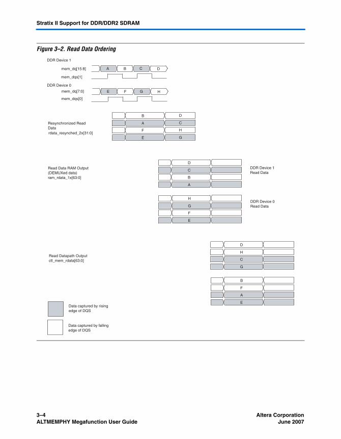
Read Data Alignment
Data alignment is the process controlled by the sequencer to ensure the correct captured read data is present in the same half-rate clock cycle at the output of the read data dual-port RAM. This is implemented using either M4K or M512 memory blocks. The concatenation of the read data into valid HDR data is shown at the bottom of Figure 3–2.
Data Mapping Steps
In this example (Figure 3–2), the memory interface consists of two 8-bit wide memory devices, resulting in a memory interface 16-bits wide.
3–4 Altera CorporationALTMEMPHY Megafunction User Guide June 2007
Stratix II Support for DDR/DDR2 SDRAM
Figure 3–2. Read Data Ordering
mem_dq[15:8]
DDR Device 1
A B C D
mem_dqs[1]
E F G H
DDR Device 0
mem_dq[7:0]
mem_dqs[0]
Resynchronized ReadDatardata_resynched_2x[31:0]
B D
A C
F H
E G
Read Data RAM Output(DEMUXed data)ram_rdata_1x[63:0]
D
C
B
A
H
G
F
E
DDR Device 1Read Data
DDR Device 0Read Data
D
H
C
G
B
F
A
E
Read Datapath Outputctl_mem_rdata[63:0]
Data captured by rising edge of DQS
Data captured by fallingedge of DQS
Altera Corporation 3–5June 2007 ALTMEMPHY Megafunction User Guide
Specifications
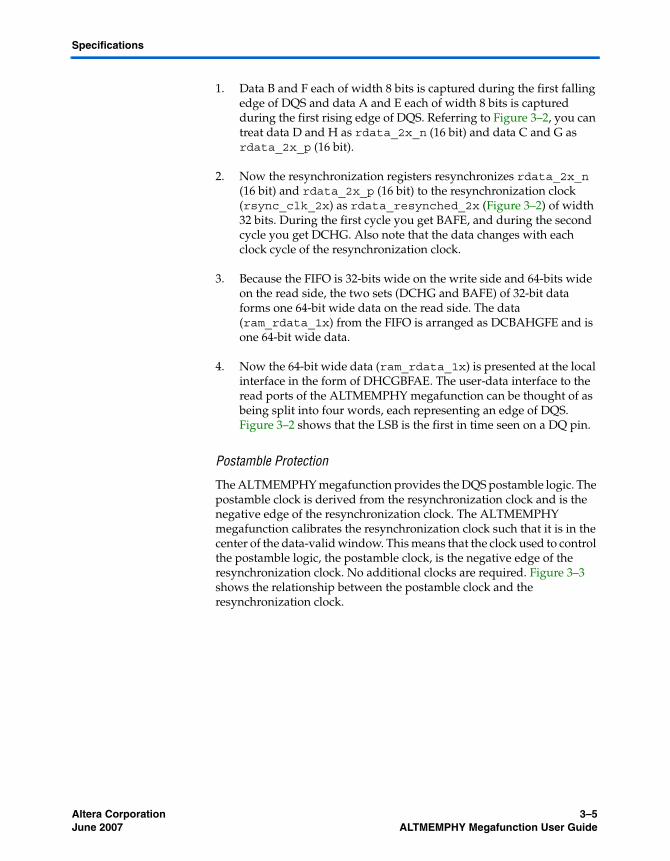
1. Data B and F each of width 8 bits is captured during the first falling edge of DQS and data A and E each of width 8 bits is captured during the first rising edge of DQS. Referring to Figure 3–2, you can treat data D and H as rdata_2x_n (16 bit) and data C and G as rdata_2x_p (16 bit).
2. Now the resynchronization registers resynchronizes rdata_2x_n (16 bit) and rdata_2x_p (16 bit) to the resynchronization clock (rsync_clk_2x) as rdata_resynched_2x (Figure 3–2) of width 32 bits. During the first cycle you get BAFE, and during the second cycle you get DCHG. Also note that the data changes with each clock cycle of the resynchronization clock.
3. Because the FIFO is 32-bits wide on the write side and 64-bits wide on the read side, the two sets (DCHG and BAFE) of 32-bit data forms one 64-bit wide data on the read side. The data (ram_rdata_1x) from the FIFO is arranged as DCBAHGFE and is one 64-bit wide data.
4. Now the 64-bit wide data (ram_rdata_1x) is presented at the local interface in the form of DHCGBFAE. The user-data interface to the read ports of the ALTMEMPHY megafunction can be thought of as being split into four words, each representing an edge of DQS. Figure 3–2 shows that the LSB is the first in time seen on a DQ pin.
Postamble Protection
The ALTMEMPHY megafunction provides the DQS postamble logic. The postamble clock is derived from the resynchronization clock and is the negative edge of the resynchronization clock. The ALTMEMPHY megafunction calibrates the resynchronization clock such that it is in the center of the data-valid window. This means that the clock used to control the postamble logic, the postamble clock, is the negative edge of the resynchronization clock. No additional clocks are required. Figure 3–3 shows the relationship between the postamble clock and the resynchronization clock.

3–6 Altera CorporationALTMEMPHY Megafunction User Guide June 2007
Stratix II Support for DDR/DDR2 SDRAM
Figure 3–3. Relationship Between Postamble Clock and Resynchronization Clock Note (1)
Note to Figure 3–3:(1) resync_clk_2x is delayed further to allow for the I/O element (IOE) to core transition time.
f For more information about the postamble circuitry, refer to the External Memory Interfaces chapter in the Stratix II Device Handbook.
Clock and Reset Management
The clocking and reset block is responsible for clock generation, reset management, and phase shifting of clocks, as well as control of clock network types used to route the clocks.
The ability of the ALTMEMPHY megafunction to work out the optimum resynchronization clock phase during calibration, and to track the system voltage and temperature (VT) variations, relies upon phase shifting the clocks relative to each other.
Clock management circuitry is implemented by using the following device resources:
■ PLL■ PLL reconfiguration■ DLL
resync_clk_2x
postamble_clk
H1 H2 L2L1
dqs (90˚ shifted)
dq
Data input to resync reg's
ARST at postamble reg's
H1L1 H2L2
Altera Corporation 3–7June 2007 ALTMEMPHY Megafunction User Guide
Specifications
PLL
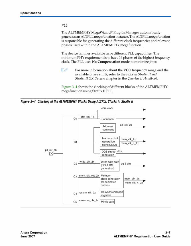
The ALTMEMPHY MegaWizard® Plug-In Manager automatically generates an ALTPLL megafunction instance. The ALTPLL megafunction is responsible for generating the different clock frequencies and relevant phases used within the ALTMEMPHY megafunction.
The device families available have different PLL capabilities. The minimum PHY requirement is to have 16 phases of the highest frequency clock. The PLL uses No Compensation mode to minimize jitter.
1 For more information about the VCO frequency range and the available phase shifts, refer to the PLLs in Stratix II and Stratix II GX Devices chapter in the Quartus II Handbook.
Figure 3–4 shows the clocking of different blocks of the ALTMEMPHY megafunction using Stratix II PLL.
Figure 3–4. Clocking of the ALTMEMPHY Blocks Using ALTPLL Clocks in Stratix II
Sequencer
core clock
phy_clk_1xC0
C1
Write data path(DQ & DMgeneration)
dq & dmC2write_clk_2x
resync_clk_2x Resynchronizationregisters
Mimic path
C3
C4
pll_ref_clk
C5measure_clk_2x
mem_clk_ext_2x Memoryclock generationfor dedicated outputs
mem_clk_2x
mem_clk_n_2x
Address/command
ac_clk_2x
Memory clockgenerationusing DDIOs
mem_clk_2x
mem_clk_n_2x
DQS strobegeneration
dqs
3–8 Altera CorporationALTMEMPHY Megafunction User Guide June 2007
Stratix II Support for DDR/DDR2 SDRAM
Table 3–1 shows the Stratix II PLL clock outputs.
Table 3–1. Stratix II PLL Clock Outputs
Clock Name (1) Postscale Counter
Phase(Degrees)
Half-Rate/Full-Rate
Clock Network Type Notes
phy_clk_1x C0 0 Half-rate Global This is the only clock that is made available on the user interface of the ALTMEMPHY megafunction.
mem_clk_2x C1 0 Full-rate Global This clock is used for clocking DQS and as a reference clock for the memory devices.
write_clk_2x C2 -90 Full-rate Global This clock is used for clocking the data out of the double-data rate input/output (DDIO) pins in advance of the DQS strobe (or equivalent). As a result, its phase leads that of the mem_clk_2x by 90°.
mem_clk_ext_2x C3 > 0 Full-rate Dedicated This clock is only used if the memory clock generation uses dedicated output pins.
resync_clk_2x C4 Calibrated Full-rate Regional This clock is used to clock the resynchronization registers after the capture registers. Its phase is adjusted to the center of the data valid window across all the DQS-clocked DDIO groups.
measure_clk_2x C5 Calibrated Full-rate Regional This clock is used for VT tracking. This free-running clock is used to measure relative phase shifts between the internal clock(s) and those being fed back through a mimic path. As a result, the ALTMEMPHY megafunction can track VT effects on the FPGA and compensate for the effects.
ac_clk_2x - 0, 90,180, 270 Full-rate Global The ac_clk_2x clock is derived from mem_clk_2x or write_clk_2x.
Note to Table 3–1:(1) The _1x clock represents a frequency that is half of the memory clock frequency; the _2x clock represents the memory
clock frequency.

Altera Corporation 3–9June 2007 ALTMEMPHY Megafunction User Guide
Specifications
ALTPLL_RECONFIG
The ALTMEMPHY MegaWizard Plug-In Manager automatically generates an ALTPLL_RECONFIG instance to match the generated ALTPLL megafunction instance. The ALTPLL_RECONFIG is used to vary the resynchronization clock phase as well as the measure clock phase.
Hard Copy II Support
The Quartus® II version 7.1 software and onwards offers support for Hard Copy® II devices and also has the Enable external access to configure PLL prior to calibration option, as shown in Figure 3–5.
Figure 3–5. Settings to Enable External Access to Reconfigure PLL
3–10 Altera CorporationALTMEMPHY Megafunction User Guide June 2007
Stratix II Support for DDR/DDR2 SDRAM
By enabling the Enable external access to configure PLL prior to calibration option, the ports of ALTPLL_RECONFIG are brought to the top level. You need to reconfigure the PLL before calibration to adjust, if necessary, the phase of the memory clock (mem_clk_2x) before the start of the calibration of the resyncronization clock on the read side. The calibration of the resynchronization clock on the read side depends on the phase of the memory clock on the write side.
1 Altera® recommends you enable this option for HardCopy II devices. When you use ALTDDIO for the memory clock, both the memory clock and the DQS signals are well aligned. When the dedicated clock outputs are used for the memory clock, the memory clock and the DQS signals are not aligned properly and will require a positive phase offset.
DLL
A DLL instance is included in the generated ALTMEMPHY variation for the Stratix series, HardCopy II, and Arria™ GX devices. When using the DQS to capture the DQ read data, the DLL center-aligns the DQS strobe to the DQ data.
1 For more information, refer to the External Memory Interfaces chapter in the Stratix II Device Handbook or the Stratix II GX Device Handbook.
Reset Management
The reset management block is responsible for the following:
■ Provides appropriately timed resets to the ALTMEMPHY megafunction datapaths and functional modules
■ Performs the reset sequencing required for different clock domains■ Provides reset management of PLL and PLL reconfiguration
functions■ Manages any circuit-specific reset sequencing
Each reset is asynchronous assert and synchronous de-assert on the appropriate clock domain. The reset management design uses a standard two-register synchronizer to avoid metastability.

Altera Corporation 3–11June 2007 ALTMEMPHY Megafunction User Guide
Specifications
Write Datapath
The write datapath logic efficiently transfers data from the HDR memory controller to DDR SDRAM-based memories. The write datapath logic consists of:
■ DQ and DQ output-enable logic ■ DQS and DQS output-enable logic■ Data mask (DM) logic
Overview
The memory controller interface outputs 4n-bit wide data (clt_mem_wdata[4n]) at half-rate frequency. Figure 3–6 shows that the HDR write data (ctl_mem_wdata[4n]) is clocked by the half-rate clock phy_clk_1x and is converted into SDR which is represented by wdp_wdata_h and wdp_wdata_l.
The DQ IOEs convert 2-n SDR bits to n-DDR bits.
Figure 3–6. Stratix II Write Datapath
Data Mapping
The write data at the controller, which is 4n-bit wide, is converted to n bits at the memory interface. Figure 3–7 shows how the ctl_mem_wdata is mapped into the mem_dq by using a 64-bit ctl_mem_wdata as an example.
Write DatapathStratix II IOE
wdp_wdata_l
phy_clk_1x
DQ
DQ
OE
DQ[n]
write_clk_2x
ctl_mem_wdata[4n]
write_clk_2x
DataMultiplexing
wdp_wdata_h
3–12 Altera CorporationALTMEMPHY Megafunction User Guide June 2007
Stratix II Support for DDR/DDR2 SDRAM
1 This is the reverse of the steps required for the read. For details, refer to “Read Data Alignment” on page 3–3.
Figure 3–7. Data Mapping Along the Write Datapath
Address and Command Datapath
The address and command datapath is responsible for taking the address and command outputs from the controller and converting them from half-rate clock to full-rate clock. Two types of addressing are possible:
■ 1T—The duration of the address and command is a single memory-clock cycle (mem_clk_2x, Figure 3–8).
■ 2T—The duration of the address and command is two memory-clock cycles. For the half-rate controller, the ALTMEMPHY megafunction supports only a burst size of four, which means the burst size on the
D
H
C
G
B
F
A
E
mem_dq[15:8]
DDR Device 1
A B C D
mem_dqs[1]
E F G H
DDR Device 0
mem_dq[7:0]
mem_dqs[0]
ctl_mem_wdata[63:0]
Data captured by rising edge of DQS
Data captured by fallingedge of DQS

Altera Corporation 3–13June 2007 ALTMEMPHY Megafunction User Guide
Specifications
local interface is always set to 1. The size of the data is 4n-bits wide on the local side and is n-bits wide on the memory side. To transfer all the 4n-bits at the double-data rate, two memory-clock cycles are required. This means that the new address and command can be issued to the memory every two clock cycles.
1 Refer to Table 3–1 in “PLL” on page 3–7 to see the frequency relationship of mem_clk_2x with the rest of the clocks.
Figure 3–8 shows a 1T chip select signal (mem_cs_n), which is active low, and disables the command in the memory device. All commands are masked when the chip-select signal is inactive. The mem_cs_n signal is considered part of the command code.
Figure 3–8. Stratix II Address and Command Datapath
The command interface is made up of the signals mem_ras_n, mem_cas_n, mem_we_n, mem_cs_n, mem_cke, and mem_odt.
The waveform in Figure 3–8 shows a NOP command followed by five back-to-back write commands.
1. The commands are asserted either on the raising or falling edge of ac_clk_2x (this depends upon the setting of the address and command clock phase, as shown in Figures 3–10 to 3–14). The outputs remain on the bus for two clock cycles, allowing sufficient time for the signals to settle.
Command
ac_clk_2x
mem_addr
mem_ba
mem_cs_n
mem_ras_n
mem_cas_n
mem_we_n
mem_dq
1
2 4 4 4
NOP NOP
3 3 3
mem-dqs
PHY Command Outputs
1
NOP NOPPCH ACT WR
0000
00
0001 0000 0004 0008 000C 0010 0000

3–14 Altera CorporationALTMEMPHY Megafunction User Guide June 2007
Stratix II Support for DDR/DDR2 SDRAM
2. On the next falling edge of ac_clk_2x, the chip select signal, mem_cs_n, is asserted low and the memory sees the command which has already been on the bus for a cycle.
3. By asserting the chip-select signal in alternative cycles, back-to-back read or write commands can be issued.
4. The address is incremented every other ac_clk_2x cycle.
1 The address and command outputs to the memory are generated according to the settings of the address and command clock (ac_clk_2x) in the PHY settings page, as shown in Figure 3–9. The phase of the address and command clock is chosen to meet the setup and hold-time requirements of the address and command signals with respect to the memory clock.
Figure 3–9. Choosing the Right Phase for the Address/Command Clock

Altera Corporation 3–15June 2007 ALTMEMPHY Megafunction User Guide
Specifications
Figures 3–10 through 3–13 show the assertion of the command signals with respect to different ac_clk_2x phase settings.
Figure 3–10. Address and Command Clock (0° Phase)
Figure 3–11. Address and Command Clock (90° Phase)
Command
ac_clk_2x
mem_cas_n
mem_cs_n
mem_ras_n
mem_we_n
PHY Command Outputs
NOP NOP
clk_to_ram
WR WR NOP WR WRNOP NOP WR NOP
Command
ac_clk_2x
mem_cas_n
mem_cs_n
mem_ras_n
mem_we_n
PHY Command Outputs
clk_to_ram
PCH NOP ACT NOP RD NOP RD NOP RD
3–16 Altera CorporationALTMEMPHY Megafunction User Guide June 2007
Stratix II Support for DDR/DDR2 SDRAM
Figure 3–12. Address and Command Clock (180° Phase)
Figure 3–13. Address and Command Clock (270° Phase)
f Observe the phase of ac_clk_2x with respect to the memory clock (clk_to_sdram) to understand the assertion of command signals with respect to the different phase settings of ac_clk_2x. For example, in both the 180° and 270° phase for ac_clk_2x, the commands are asserted along with the positive edge of ac_clk_2x, but the relationship between ac_clk_2x and clk_to_sdram is different for 180° and 270°.
f Refer to the External Memory Interfaces chapter in the Stratix II Device Handbook or the Stratix II GX Device Handbook for help in selecting I/O pins for the address and command signals.
Command
ac_clk_2x
mem_cas_n
mem_cs_n
mem_ras_n
mem_we_n
PHY Command Outputs
PCH ACT
clk_to_ram
NOP NOP WR WRNOP NOP WR NOP
Command
ac_clk_2x
mem_cas_n
mem_cs_n
mem_ras_n
mem_we_n
PHY Command Outputs
clk_to_ram
NOP WR NOPNOP WR NOP WR NOP WR WR NOP
Altera Corporation 3–17June 2007 ALTMEMPHY Megafunction User Guide
Specifications
Full-Rate Support
The following section discusses full-rate support.
Read Data Path
The full-rate datapath is similar to the half-rate datapath except that the function performed along the full-rate datapath is only data capture and resynchronization. The full-rate data path also consists of a RAM with the same width as the data input (just like that of the half-rate), but the width on the data output of the RAM is half that of the half-rate PHY. The function of the RAM is to transfer the read data from the resynchronization clock domain to system clock domain.
Postamble Protection
The postamble protection is the same as the half-rate support (refer to “Half-Rate Support” on page 3–1 for more information).
Clock and Reset Management
Clock and reset management is similar to half-rate support except that the phy_clk_1x clock defined in Table 3–3, is now a full-rate clock and is derived from mem_clk_2x (refer to “Half-Rate Support” on page 3–1 for more information).
1 phy_clk_1x is now full-rate, despite the "1x" naming convention.
Write Data Path
The write datapath is similar to the half-rate PHY. The I/O element (IOE) block is identical to the half-rate PHY. The latency of the write datapath in the full-rate PHY is less than in the half-rate PHY because the full-rate PHY is free from the half-rate-to-full-rate conversion logic.
1 Refer to “Latency Numbers” on page A–1 for more information on latency figures.
Address and Command DataPath
The address and command datapath is based on 1T addressing. For the full-rate PHY, the ALTMEMPHY supports only a burst size of four on the memory interface, which in turn equals a burst size of two on the local interface. Since the burst size is fixed at four for the memory interface, it takes two memory clock cycles to either read or write data that is

3–18 Altera CorporationALTMEMPHY Megafunction User Guide June 2007
Stratix III Support for DDR/DDR2/ SDRAM and QDRII/QDRII+ SRAM
requested at the local interface, as shown in Figure 3–14. Since the address and command is 1T, the controller will be inserting a NOP command between every read and write command.
Figure 3–14. Stratix II Full-Rate Address and Command
Stratix III Support for DDR/DDR2/SDRAM andQDRII/QDRII+ SRAM
Half-Rate Support
The following section discusses half-rate support.
Read Datapath
The Stratix III read datapath (Figure 3–15) consists of two main blocks:
■ Data Capture, Resynchronization, and Demultiplexing■ Read Datapath logic (Read Datapath)
Command
ac_clk_2x
mem_cas_n
mem_cs_n
mem_ras_n
mem_we_n
PHY Command Outputs
clk_to_ram
NOP WR NOPNOP WR NOP WR NOP WR WR NOP
a_delayed
mem_dq
0000 0004 0000 0008 0000 000c 0000 0010 0000
00000000 946... ab9... 35c... 4b3... 6a9... 967... d42f... 31e... b55... 62d... 77b... c4b... ee6... 597... c1c... 37e... 9f89...
Altera Corporation 3–19June 2007 ALTMEMPHY Megafunction User Guide
Specifications
Figure 3–15. Data Capture and Read Data Mapping in Stratix III
Data Capture, Resynchronization, and Demultiplexing
In Stratix III devices, the smart interface module in the IOE performs the following tasks:
■ Captures the data■ Resynchronizes the captured data from the DQS domain to the
resynchronization clock (resync_clk_2x) domain ■ Converts the resynchronized data into half-data rate (HDR) data.
This is performed by feeding the resynchronized data into the HDR conversion block within the IOE, which is clocked by the half-rate version of the resynchronization clock.
f For more information about IOE registers, refer to the External Memory Interfaces in Stratix III Devices chapter of the Stratix III Device Handbook.
Data Resynchronization and Read Data Mapping
The read datapath block performs the following two tasks:
1. Transfers the captured read data (rdata[n]_1x) from the half-rate resynchronization clock (resynck_clk_1x) domain to the half-rate system clock (phy_clk_1x) domain using dual port RAM. Resynchronized data from the FIFO is shown as ram_data_1x.
2. Reorders the resynchronized data (ram_rdata_1x) into ctl_mem_rdata.
FIFO
Read DatapathData Capture, Resynchronization,and Data Demultiplexing
mem_dq
rdata3_1x
seq_dq_dm_add_delay
IOE
mem_dqs
mem_dqs_n
rdata2_1x
rdata1_1x
rdata0_1x
resync_clk_1x
resync_clk_2x
4n bitswr_data
wr_clk
rd_data
rd_clk
ctl_mem_rdata[4n]ram_rdata_1x[4n]
phy_clk_1x
Data MappingLogic

3–20 Altera CorporationALTMEMPHY Megafunction User Guide June 2007
Stratix III Support for DDR/DDR2/ SDRAM and QDRII/QDRII+ SRAM
1 The data bus for QDRII/QDRII+ SRAM is unidirectional when compared to DDR/DDR2 SDRAM. The read data bus is mem_dq and the write data bus is mem_d for QDRII and QDRII+ SRAM implementation.
Postamble Protection
Stratix III devices have a dedicated postamble register that can be controlled to gate the shifted DQS signal used to clock the DQ input registers at the end of a read operation. This ensures that any glitches on the DQS input signals at the end of the read postamble time do not cause erroneous data to be captured as a result of postamble glitches.
f For more information about the postamble protection circuitry, refer to the External Memory Interfaces for Stratix III Devices chapter in the Stratix III Device Handbook.
1 For QDRII/QDRII+ SRAM, postamble protection circuitry is not needed as the data from the memory is captured on a free running read (cq) clock.
Clock and Reset Management
The clocking and reset block is responsible for clock generation, reset management, and phase shifting of clocks as well as control of clock network types used to route the clocks.
The ability of the ALTMEMPHY megafunction to work out the optimum phase during calibration and to track voltage and temperature variation relies on phase shifting the clocks relative to each other. Note that certain clocks need to be phase shifted during the ALTMEMPHY megafunction operation.
Clock management circuitry is implemented by using:
■ PLL■ DLL
PLL
The ALTMEMPHY MegaWizard Plug-In Manager automatically generates an ALTPLL megafunction instance. The ALTPLL megafunction is responsible for generating the different clock frequencies and relevant phases used within the ALTMEMPHY megafunction.
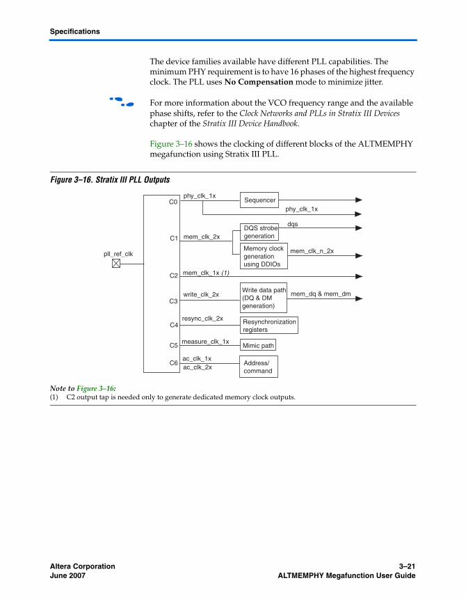
Altera Corporation 3–21June 2007 ALTMEMPHY Megafunction User Guide
Specifications
The device families available have different PLL capabilities. The minimum PHY requirement is to have 16 phases of the highest frequency clock. The PLL uses No Compensation mode to minimize jitter.
f For more information about the VCO frequency range and the available phase shifts, refer to the Clock Networks and PLLs in Stratix III Devices chapter of the Stratix III Device Handbook.
Figure 3–16 shows the clocking of different blocks of the ALTMEMPHY megafunction using Stratix III PLL.
Figure 3–16. Stratix III PLL Outputs
Note to Figure 3–16:(1) C2 output tap is needed only to generate dedicated memory clock outputs.
Sequencerphy_clk_1x
DQS strobegeneration
dqs
mem_clk_2x
Memory clockgenerationusing DDIOs
mem_clk_n_2x
C0
C1
Write data path(DQ & DMgeneration)
mem_dq & mem_dm
C2
write_clk_2x
resync_clk_2x
ac_clk_1x
Resynchronizationregisters
Mimic path
ac_clk_2xAddress/command
C3
C4
pll_ref_clk
mem_clk_1x (1)
C5measure_clk_1x
C6
phy_clk_1x
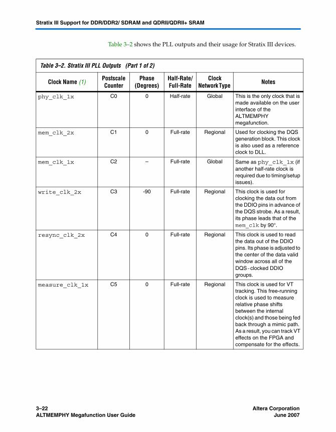
3–22 Altera CorporationALTMEMPHY Megafunction User Guide June 2007
Stratix III Support for DDR/DDR2/ SDRAM and QDRII/QDRII+ SRAM
Table 3–2 shows the PLL outputs and their usage for Stratix III devices.
Table 3–2. Stratix III PLL Outputs (Part 1 of 2)
Clock Name (1) Postscale Counter
Phase(Degrees)
Half-Rate/Full-Rate
Clock Network Type Notes
phy_clk_1x C0 0 Half-rate Global This is the only clock that is made available on the user interface of the ALTMEMPHY megafunction.
mem_clk_2x C1 0 Full-rate Regional Used for clocking the DQS generation block. This clock is also used as a reference clock to DLL.
mem_clk_1x C2 – Full-rate Global Same as phy_clk_1x (if another half-rate clock is required due to timing/setup issues).
write_clk_2x C3 -90 Full-rate Regional This clock is used for clocking the data out from the DDIO pins in advance of the DQS strobe. As a result, its phase leads that of the mem_clk by 90°.
resync_clk_2x C4 0 Full-rate Regional This clock is used to read the data out of the DDIO pins. Its phase is adjusted to the center of the data valid window across all of the DQS-clocked DDIO groups.
measure_clk_1x C5 0 Full-rate Regional This clock is used for VT tracking. This free-running clock is used to measure relative phase shifts between the internal clock(s) and those being fed back through a mimic path. As a result, you can track VT effects on the FPGA and compensate for the effects.

Altera Corporation 3–23June 2007 ALTMEMPHY Megafunction User Guide
Specifications
1 For Stratix III devices, the PLL reconfiguration is done using the phase-shift inputs on the PLL. The PLL reconfiguration megafunction is not required.
DLL
The DLL for Stratix III devices is instantiated in the same way as for Stratix II devices. Refer to the External Memory Interfaces in Stratix III Devices chapter of the Stratix III Device Handbook for more information.
Reset Management
The reset management for Stratix III devices is instantiated in the same way as it is with Stratix II devices. Refer to “Reset Management” on page 3–10.
Write Datapath
The memory controller interface outputs 4 n-bit wide data (ctl_mem_wdata) at phy_clk_1x frequency. The write data is clocked by the system clock phy_clk_1x at half-data rate (HDR) and reordered into HDR of width 4 n-bits represented in Figure 3–17 by wdp_wdata3_1x, wdp_wdata2_1x, wdp_wdata1_1x and wdp_wdata0_1x.
As Figure 3–17 shows, the reordered or the reordered-and-delayed HDR data is then converted to DDR data within the IOE element using both the half-rate and full-rate clocks.
ac_clk_1x C6 Determined using timing
analysis
Half-rate Regional Address and command clock.
Note to Table 3–2:(1) The _1x notation represents a frequency that is half of the memory clock frequency; the _2x notation represents
the memory clock frequency.
Table 3–2. Stratix III PLL Outputs (Part 2 of 2)
Clock Name (1) Postscale Counter
Phase(Degrees)
Half-Rate/Full-Rate
Clock Network Type Notes

3–24 Altera CorporationALTMEMPHY Megafunction User Guide June 2007
Stratix III Support for DDR/DDR2/ SDRAM and QDRII/QDRII+ SRAM
Figure 3–17. Write Datapath in Stratix III Devices
The main difference between the Stratix II and Stratix III write datapaths is that all of the write datapath registers in the Stratix III device are clocked by the half-rate clock, phy_clk_1x.
1 For more information about the Stratix III I/O structure, refer to the External Memory Interface in Stratix III Devices chapter of the Stratix III Device Handbook.
Data Mapping
The write data mapping for Stratix III devices is identical to the mapping defined for Stratix II devices. Refer to “Data Mapping” on page 3–11.
1 The data bus for QDRII/QDRII+ SRAM is unidirectional when compared to DDR/DDR2 SDRAM. The read data bus is mem_dq and the write data bus is mem_d for QDRII and QDRII+ SRAM implementation.
Address and Command Datapath
The address and command datapath is similar to Stratix II devices, as described in “Address and Command Datapath” on page 3–12. The only difference is that in Stratix II designs, the address and command clock is configured to be write_clk_2x or mem_clk_2x. For Stratix III devices,
DataOrdering
mem_dq Stratix IIIIOE
write_clk_2x
phy_clk_1
seq_dq_dm_add_delay
ctl_mem_wdata[4n]
phy_clk_1x
wdp_wdata3_1x
wdp_wdata2_1xwdp_wdata1_1x
wdp_wdata0_1x

Altera Corporation 3–25June 2007 ALTMEMPHY Megafunction User Guide
Specifications
the address and command clock is one of the PLL dedicated clock outputs whose phase can be adjusted to meet the setup and hold requirements of the memory clock.
Full-Rate Support
There is no full-rate support in the Quartus II version 7.1 software.
Arria GX Support for DDR/DDR2 SDRAM
Operation of the Arria GX device is similar to the Stratix II device. Refer to “Stratix II Support for DDR/DDR2 SDRAM” on page 3–1 for more information.
Cyclone III Support for DDR/DDR2SDRAM
Half-Rate Support
The following section discusses half-rate support.
Read Datapath
Figure 3–18 shows the Cyclone® III read datapath for a single DQ pin. The diagram shows a half-rate read path where four data bits are produced for each DQ pin. Unlike Stratix II and Stratix III devices, data capture is entirely done in the core logic since the IOE does not contain DDIO capture registers.
Figure 3–18. Cyclone III Read Datapath
DQ
resynck_clk_2x
FIFO
wr_data rd_data4-bits/DQ
phy_clk
read_data
Data Capture Data Resynchronization Data Demux & Alignment
D Q D Q
D Q D Q D Q

3–26 Altera CorporationALTMEMPHY Megafunction User Guide June 2007
Cyclone III Support for DDR/DDR2 SDRAM
Capture and Pipelining
The DDR and DDR2 SDRAM read data is captured using registers in the Cyclone III FPGA core. These capture registers are clocked using the capture clock (resynch_clk_2x, refer to Figure 3–18). The captured read data generates two data bits per DQ pin; one data bit for the read data captured by the rising edge of the capture clock and one data bit for the read data captured by the falling edge of the capture clock.
After the read data has been captured, it may be necessary to insert registers in the read datapath between the capture registers and the read data FIFO to help meet timing. These registers are known as pipeline registers and are clocked off the same clock used by the capture registers, the capture clock (resync_clk_2x).
Data Demultiplexing
The data demultiplexing for Cyclone III devices is instantiated in the same way as it is with Stratix II devices. Refer to “Data Demultiplexing” on page 3–2 for more information.
Data Mapping
The data alignment for Cyclone III devices is instantiated in the same way as it is with Stratix II devices. Refer to “Data Mapping Steps” on page 3–3 for more information.
Postamble Protection
Postamble protection circuitry is not required in the Cyclone III device implementation as DQS mode capture of the DQ data is not supported. The data capture is done using the clock (resync_clk_2x) generated from the ALTPLL megafunction.
Clock and Reset Management
Clock management circuitry is implemented using the ALTPLL megafunction.
PLL
The ALTPLL megafunction is instantiated within the ALTMEMPHY megafunction and is responsible for generating all the clocks used by the ALTMEMPHY and the memory controller. Table 3–3 shows the clocks generated by the ALTPLL megafunction.
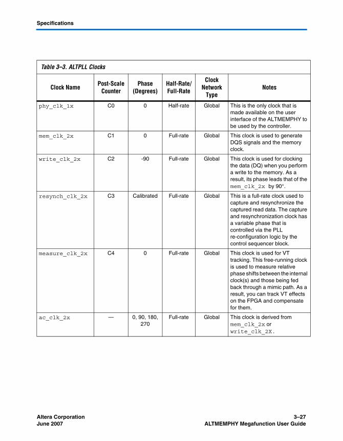
Altera Corporation 3–27June 2007 ALTMEMPHY Megafunction User Guide
Specifications
Table 3–3. ALTPLL Clocks
Clock Name Post-Scale Counter
Phase(Degrees)
Half-Rate/Full-Rate
Clock Network
TypeNotes
phy_clk_1x C0 0 Half-rate Global This is the only clock that is made available on the user interface of the ALTMEMPHY to be used by the controller.
mem_clk_2x C1 0 Full-rate Global This clock is used to generate DQS signals and the memory clock.
write_clk_2x C2 -90 Full-rate Global This clock is used for clocking the data (DQ) when you perform a write to the memory. As a result, its phase leads that of the mem_clk_2x by 90°.
resynch_clk_2x C3 Calibrated Full-rate Global This is a full-rate clock used to capture and resynchronize the captured read data. The capture and resynchronization clock has a variable phase that is controlled via the PLL re-configuration logic by the control sequencer block.
measure_clk_2x C4 0 Full-rate Global This clock is used for VT tracking. This free-running clock is used to measure relative phase shifts between the internal clock(s) and those being fed back through a mimic path. As a result, you can track VT effects on the FPGA and compensate for them.
ac_clk_2x — 0, 90, 180, 270
Full-rate Global This clock is derived from mem_clk_2x or write_clk_2X.

3–28 Altera CorporationALTMEMPHY Megafunction User Guide June 2007
Cyclone III Support for DDR/DDR2 SDRAM
Figure 3–19. Cyclone III ALTPLL Clock Outputs
Reset Management
The reset management for Cyclone III devices is instantiated in the same way as it is with Stratix II devices. Refer to “Reset Management” on page 3–10 for more information.
Write Datapath
The write datapath for Cyclone III devices is instantiated in the same way as it is with Stratix II devices. Refer to “Write Datapath” on page 3–11 for more information.
Address and Command Datapath
The full-rate support for Cyclone III devices is similar to the Stratix II device. Refer to “Address and Command Datapath” on page 3–12 for more information.
Sequencer
phy_clk_1x
phy_clk_1x
DQS strobegeneration
dqsmem_clk_2x
Memory clockgenerationusing DDIOs
mem_clk_2x
mem_clk_n_2x
C0
C1
Write data path(DQ & DMgeneration) dq & dm
C2write_clk_2x
resync_clk_2x
measure_clk_2x
Capture/recaptureregisters
Mimic path
ac_clk_2x Address/command
C3
C4
pll_ref_clk

Altera Corporation 3–29June 2007 ALTMEMPHY Megafunction User Guide
Specifications
Full-Rate Support
The full-rate support for Cyclone III devices is similar to the Stratix II device. Refer to “Full-Rate Support” on page 3–17 for more information.
Read Datapath
The read datapath for Cyclone III devices similar to the Stratix II device. Refer to “Read Data Path” on page 3–17 for more information.
Postamble Protection
There is no postamble protection circuitry.
Clock and Reset Management
The clock and reset management for Cyclone III devices is similar to half-rate support for Stratix II devices except that the phy_clk_1x clock defined in Table 3–3, is now a full-rate clock and is derived from mem_clk_2x.
1 phy_clk_1x is now full-rate, despite the "1x" naming convention.
Write Data Path
The write data path is free from half-rate-to-full-rate conversion logic that was in the half-rate controller. The IOE block is identical to the half-rate controller. Because of the RAM exclusion, the latency of the write data path is smaller in the full-rate controller as compared to the half-rate controller.
1 Refer to “Selection Criteria Between ALTMEMPHY & Legacy Controllers” on page A–1 for more information on latency figures.
Address and Command Datapath
The address and command datapath is similar to Stratix II full-rate address and command datapath.
Read Datapath
The read datapath is the same as the Stratix II full-rate datapath.

3–30 Altera CorporationALTMEMPHY Megafunction User Guide June 2007
Calibration
Postamble Protection
The postamble protection is the same as the Stratix II half-rate support.
Clock and Reset Management
The clock and reset management is similar to half-rate support except for the clock phy_clk_1x defined in Table 3–3, is now a full-rate clock and is derived from mem_clk_2x.
1 phy_clk_1x is now full-rate, despite the "1x" naming convention.
Write Data Path
The IOE block is identical to the half-rate PHY. The latency of the write data path is smaller in the full-rate PHY as compared to the half-rate PHY because the full-rate PHY is free from the half-rate-to-full-rate conversion logic that was there in the half-rate PHY.
1 Refer to “Selection Criteria Between ALTMEMPHY & Legacy Controllers” on page A–1 for more information on latency figures.
Address and Command Datapath
The address and command datapath is the same as that of the Stratix II full-rate address and command datapath.
Calibration DDR/DDR2 SDRAM
At power-up, the ALTMEMPHY megafunction calibrates out any process variance on the DDR/DDR2 device and the external memory device to establish the resynchronization clock phase which provides the greatest timing margin. This removes many of the uncertainties from the read datapath delay and achieves a higher frequency of operation across process, voltage, and temperature (PVT).
The sequencer is an element of the ALTMEMPHY megafunction designed to perform this path-delay analysis to set up the resynchronization clock and data alignment settings.
Figure 3–20 shows that the various stages of the sequence of operation of the ALTMEMPHY megafunction are further divided into a series of tasks which are performed by the sequencer.
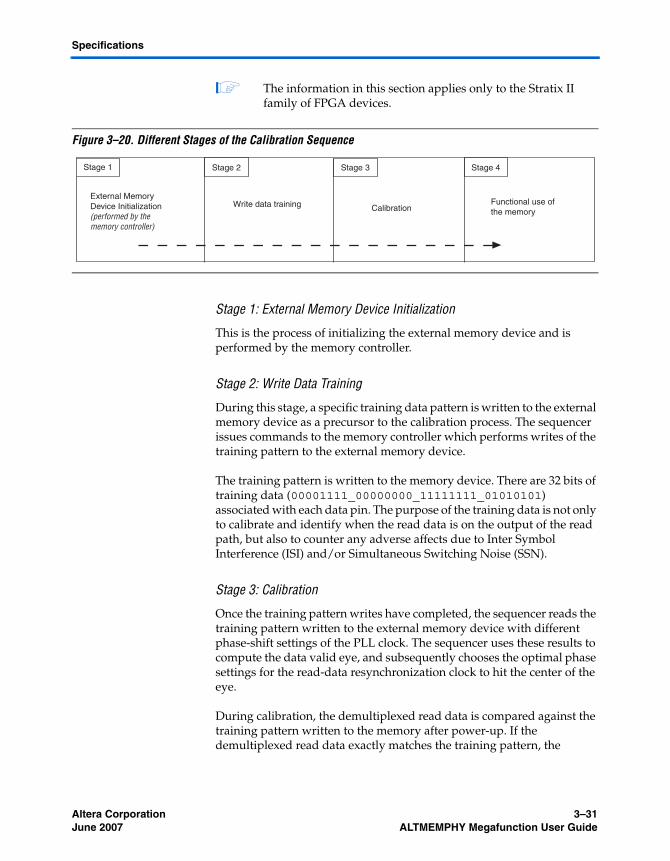
Altera Corporation 3–31June 2007 ALTMEMPHY Megafunction User Guide
Specifications
1 The information in this section applies only to the Stratix II family of FPGA devices.
Figure 3–20. Different Stages of the Calibration Sequence
Stage 1: External Memory Device Initialization
This is the process of initializing the external memory device and is performed by the memory controller.
Stage 2: Write Data Training
During this stage, a specific training data pattern is written to the external memory device as a precursor to the calibration process. The sequencer issues commands to the memory controller which performs writes of the training pattern to the external memory device.
The training pattern is written to the memory device. There are 32 bits of training data (00001111_00000000_11111111_01010101) associated with each data pin. The purpose of the training data is not only to calibrate and identify when the read data is on the output of the read path, but also to counter any adverse affects due to Inter Symbol Interference (ISI) and/or Simultaneous Switching Noise (SSN).
Stage 3: Calibration
Once the training pattern writes have completed, the sequencer reads the training pattern written to the external memory device with different phase-shift settings of the PLL clock. The sequencer uses these results to compute the data valid eye, and subsequently chooses the optimal phase settings for the read-data resynchronization clock to hit the center of the eye.
During calibration, the demultiplexed read data is compared against the training pattern written to the memory after power-up. If the demultiplexed read data exactly matches the training pattern, the
Stage 1 Stage 2 Stage 3 Stage 4
External MemoryDevice Initialization(performed by thememory controller)
Write data training CalibrationFunctional use of the memory
3–32 Altera CorporationALTMEMPHY Megafunction User Guide June 2007
Calibration
comparison logic block signals a ‘pass’ to the control sequencer. If the demultiplexed read data does not exactly match the training pattern, the comparison logic block signals a ‘fail’ to the control sequencer.
Once a training pattern read-and-comparison operation has completed and the pass/fail result has been stored, the control sequencer uses the PLL reconfiguration logic to shift the capture and resynchronization clock phase by one VCO phase step. When the PLL re-configuration has completed, the control sequencer performs another training pattern read-and-comparison operation. This sequence continues until all PLL VCO phase taps have been tested. The training pattern read comparison is done on a by-pin basis to minimize logic. Therefore, for a 64-bit DDR2 SDRAM interface using a single read data demultiplex phase, the control sequencer performs 64 training pattern reads and comparisons before all the pass/fail results have been stored for the memory interface pins.
Once all the pins have been tested, the sequencer increments the resynchronization clock phase by one step. It then repeats the above read/pattern matching procedure for the new resynchronization clock phase.
Additionally, there are two demultiplex phases for the read-data output from the read-data RAM. The sequencer shifts the resynchronization clock through 720° for a half-rate controller and 360° for a full-rate controller. This is guaranteed to provide a correct demux phase.
Once all the pass/fail results have been stored, the control sequencer calculates the optimum resynchronization clock phase such that the resynchronization clock is placed in the center of the data valid window. Once this optimum phase has been calculated, the control sequencer uses the PLL reconfiguration logic to set up the phase of the resynchronization clock to the calculated optimum phase. Auto-calibration is now complete. This is indicated by the assertion of user_mode_ready. It also uses the correct read latency value for this clock phase setting to assert the read_data_valid signal to indicate when the local_rdata bus has valid read data on it.
Stage 4: Functional Use of the Memory
This is the normal user mode of the memory. In this stage, the memory interface is fully controlled by the user interface. This is indicated by the assertion of the user_mode_ready signal. The memory controller is driven by the sequencer or the memory controller is driven by the user logic.
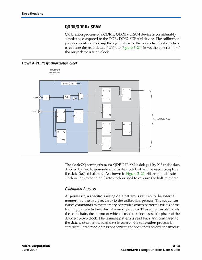
Altera Corporation 3–33June 2007 ALTMEMPHY Megafunction User Guide
Specifications
QDRII/QDRII+ SRAM
Calibration process of a QDRII/QDRII+ SRAM device is considerably simpler as compared to the DDR/DDR2 SDRAM device. The calibration process involves selecting the right phase of the resynchronization clock to capture the read data at half rate. Figure 3–21 shows the generation of the resynchronization clock.
Figure 3–21. Resynchronization Clock
The clock CQ coming from the QDRII SRAM is delayed by 90° and is then divided by two to generate a half-rate clock that will be used to capture the data (DQ) at half rate. As shown in Figure 3–21, either the half-rate clock or the inverted half-rate clock is used to capture the half-rate data.
Calibration Process
At power up, a specific training data pattern is written to the external memory device as a precursor to the calibration process. The sequencer issues commands to the memory controller which performs writes of the training pattern to the external memory device. The sequencer also loads the scan chain, the output of which is used to select a specific phase of the divide-by-two clock. The training pattern is read back and compared to the data written, if the read data is correct, the calibration process is complete. If the read data is not correct, the sequencer selects the inverse
CQ
Input from Sequencer
D Q D Q
Scan Chain
1/2-90
D Q
Q
DQ
D Q
Q
D Q
Q
D Q
Q
D Q
Q
D Q
Q
D Q
Q
Half Rate Data
3–34 Altera CorporationALTMEMPHY Megafunction User Guide June 2007
VT Tracking
of the divide-by-two clock and reads the half-rate data. This phase should be corrected and selected as the right phase of the resynchronization clock to capture the data.
VT Tracking DDR/DDR2 SDRAM
VT tracking is a background process that tracks the VT variations to maintain the relationship between the resynchronization clock and the data valid window that were achieved at calibration. This is also referred to as tracking.
Overview
The relationship between the resynchronization clock and the data valid window is maintained by measuring the mimic path variations due to the VT variations and applying the same variation to the resynchronization clock.
Mimic Path
The mimic path is used to mimic the FPGA portion of the elements of the round-trip delay. This enables the calibration sequencer to track delay variation due to VT changes during the memory read and write transactions without interrupting the operation of the ALTMEMPHY megafunction.
Figure 3–22 shows the mimic path which mimics the delay of the clock outputs to the memory as far as the pads of the FPGA and the delay from the input DQS pads to a register in the FPGA core. During the tracking operation, the calibration sequencer measures the delay of the mimic path by varying the phase of the measure clock. Any change in the delay of the mimic path indicates a corresponding change in the round-trip delay, and a corresponding adjustment is made to the phase of the resynchronization clock.
The assumption made about the mimic path is that the VT variation on the round trip delay path that resides outside of the FPGA is accounted for in the board skew and memory parameters entered in the Megawizard. For the write direction, any VT variation in the memory devices is accounted for by timing analysis.

Altera Corporation 3–35June 2007 ALTMEMPHY Megafunction User Guide
Specifications
Figure 3–22. Mimic Path
Tracking Calibration
Tracking calibration takes place once the data calibration phase has completed. During initial calibration, the mimic path is sampled using the measure clock (measure_clk has a _1x or _2x suffix, depending on the target FPGA device). The sampled value is then stored by the sequencer. Once a sample value has been stored, the sequencer uses the PLL reconfiguration logic to change the phase of the measure clock by one VCO phase tap. The control sequencer then stores the sampled value for the new mimic path clock phase. This sequence continues until all mimic path clock phase steps have been swept. Once the control sequencer has stored all the mimic path sample values, it calculates the phase which corresponds to the center of the high period of the mimic path waveform. This is the reference mimic path sampling phase. This optimum sampling phase is used during the VT tracking phase.
Tracking
Tracking is a continuous process that is transparent and is used to maintain a near-optimum resynchronization clock phase as VT varies. In user mode, the control sequencer periodically performs a tracking operation as defined in the tracking calibration description. At the end of the tracking calibration operation, the control sequencer compares the most recent optimum tracking phase against the reference sampling phase. If the sampling phases do not match, the mimic path delays have changed due to voltage and temperature variations.
padio
datain 1
ddiodatain 0
outclk
ALTPLL
mem_clk_2x
measure_clk
mimic_data_in
measure_clkalt_mem_phy_mimic
combout
3–36 Altera CorporationALTMEMPHY Megafunction User Guide June 2007
Integrating ALTMEMPHY with Your Own Controller
When the sequencer detects that the mimic path reference and most recent sampling phases do not match, the sequencer uses the PLL reconfiguration logic to change the phase of the resynchronization clock by the VCO taps in the same direction. This allows the tracking process to maintain the near-optimum capture clock phase setup during data tracking calibration as voltage and temperature vary over time.
QDRII/QDRII+ SRAM
VT Tracking
VT tracking is not required because the read strobe from the QDRII memory is continuous. This means that all registers in the I/O to the read RAM path are clocked using a clock that is derived from the QDRII read strobe.
Integrating ALTMEMPHY with Your Own Controller
The ALTMEMPHY megafunction can be integrated with your own controller. This section describes the interface requirement and the handshake mechanism for efficient read and write transactions.
Preliminary Steps
Perform the following steps to generate the ALTMEMPHY megafunction:
1. Generate the ALTMEMPHY megafunction as described in “Getting Started” on page 2–1 by selecting the desired parameters.
2. Compile and verify the timing. This step is optional; refer to “Compiling in the Quartus II Software” on page 2–16 and “Analyzing Timing” on page 2–19 for details.
3. Integrate the top-level ALTMEMPHY design with your controller. Details about integrating your controller with Altera’s ALTMEMPHY are described in the following sections.
Overview
The auto-calibration logic in the ALTMEMPHY megafunction relies on the services of the memory controller to perform its calibration writes and reads, so it must be able to have control of the controller’s local interface during the initial calibration stage. This means that the ALTMEMPHY megafunction has four interfaces that all need to be connected appropriately. Figure 3–23 shows the four interfaces.
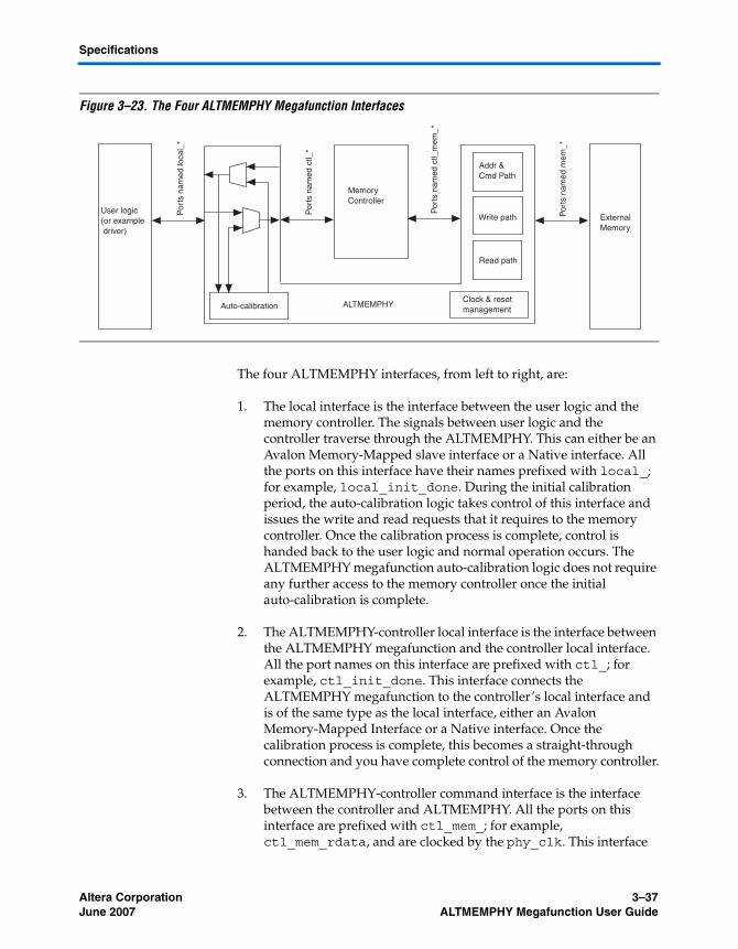
Altera Corporation 3–37June 2007 ALTMEMPHY Megafunction User Guide
Specifications
Figure 3–23. The Four ALTMEMPHY Megafunction Interfaces
The four ALTMEMPHY interfaces, from left to right, are:
1. The local interface is the interface between the user logic and the memory controller. The signals between user logic and the controller traverse through the ALTMEMPHY. This can either be an Avalon Memory-Mapped slave interface or a Native interface. All the ports on this interface have their names prefixed with local_; for example, local_init_done. During the initial calibration period, the auto-calibration logic takes control of this interface and issues the write and read requests that it requires to the memory controller. Once the calibration process is complete, control is handed back to the user logic and normal operation occurs. The ALTMEMPHY megafunction auto-calibration logic does not require any further access to the memory controller once the initial auto-calibration is complete.
2. The ALTMEMPHY-controller local interface is the interface between the ALTMEMPHY megafunction and the controller local interface. All the port names on this interface are prefixed with ctl_; for example, ctl_init_done. This interface connects the ALTMEMPHY megafunction to the controller’s local interface and is of the same type as the local interface, either an Avalon Memory-Mapped Interface or a Native interface. Once the calibration process is complete, this becomes a straight-through connection and you have complete control of the memory controller.
3. The ALTMEMPHY-controller command interface is the interface between the controller and ALTMEMPHY. All the ports on this interface are prefixed with ctl_mem_; for example, ctl_mem_rdata, and are clocked by the phy_clk. This interface
User logic(or example driver)
Auto-calibration
MemoryController
Clock & resetmanagement
ALTMEMPHY
Addr &Cmd Path
Write path
Read path
Por
ts n
amed
loca
l_*
Por
ts n
amed
ctl_
*
Por
ts n
amed
ctl_
mem
_*
Por
ts n
amed
mem
_*
External Memory
3–38 Altera CorporationALTMEMPHY Megafunction User Guide June 2007
Integrating ALTMEMPHY with Your Own Controller
contains the memory control and address signals from the controller to the memory. The controller also sends write data to, and receives read data from, the external memory through this interface. All the signals on this interface are clocked at the phy_clk rate, and the ALTMEMPHY megafunction converts between this clock and the memory interface clock.
4. The fourth interface is between the ALTMEMPHY megafunction and the external memory devices, and consists of the memory address, command, and data pins. These must be connected directly to the external pins of your Altera FPGA.
Design Considerations
There are some important considerations for implementing your own controller with the ALTMEMPHY megafunction.
Local Interface Requirements
Since the auto-calibration logic makes use of the controller to perform its calibration, your controller will have to take the following into account.
The controller must have at least one Avalon Memory-Mapped slave interface or a Native interface, as defined in the DDR SDRAM High-Performance User Guide, which the ALTMEMPHY can control during the initial calibration process. Once calibration is complete, no further access to this interface is required by ALTMEMPHY.
The memory burst length is fixed at four for DDR SDRAM or DDR2 SDRAM devices. For a half-rate controller with the memory clock running twice as fast as the clock provided to the local interface, this means that data buses on the local interface will be four times as wide as the memory data bus. For a full-rate controller, the memory clock runs at the same speed as the clock provided to the local interface, this means that the data buses on the local interface will be two times as wide as the memory data bus. This means that each read or write request on the local interface fits into a single memory read or write command on the memory interface, simplifying the controller design.
Clocks and Resets
The ALTMEMPHY megafunction automatically generates a PLL instance, but you must still provide the reference clock input (pll_ref_clk) with a clock of the frequency that you specified in the MegaWizard Plug-In Manager. An active-low global reset input is also provided which you can de-assert asynchronously. The clock and reset management logic synchronizes this to the appropriate clock domains
Altera Corporation 3–39June 2007 ALTMEMPHY Megafunction User Guide
Specifications
inside the ALTMEMPHY megafunction. A clock output, which is half the memory clock frequency for a half-rate controller and the same as the memory clock for a full-rate controller, is provided (phy_clk) and all inputs and outputs of the ALTMEMPHY megafunction are synchronous to this clock. An active-low synchronous reset is also provided (reset_phy_clk_n).
Calibration Process Requirements
Since the auto-calibration logic makes use of the controller to perform its calibration, you should follow these guidelines at power-up. Once the global reset (global_reset_n) is released, the clock management logic waits for the PLL to lock and then releases the reset to the rest of the logic, including the controller. Since the PLL locked output is gated inside the PLL, for approximately the first 10,000 cycles (by this time the PLL-locked output is stable) of the PLL reference clock, there will be no activity at this time. Once the reset to the controller (reset_phy_clk_n) has been released, the controller begins its normal memory initialization sequence. When this is complete, the controller indicates to the ALTMEMPHY megafunction that it is ready to accept the calibration writes and reads by asserting the ctl_init_done and ctl_ready signals. The auto-calibration logic then issues a series of writes and reads to the external memory. You do not have access to the memory controller during this period. Once the auto-calibration logic has completed its calibration, ALTMEMPHY asserts local_init_done and local_ready and you have complete control of the memory controller.
To calibrate the read datapath, the auto-calibration logic repeatedly requests blocks of nine consecutive read requests from the controller. The controller must be able to issue these nine read requests such that the read data, coming back into the system, is a continuous stream of data for nine clock cycles. The calibration logic is able to detect if the reads are not back-to-back and can cope with some interrupted streams; for example, if the controller has to issue a periodic refresh. The auto-calibration logic repeats that block of reads if it detects that the data was not contiguous.
Half Rate Controller
Handshake Mechanism Between Read Commands and Read Data
The controller generates a signal (ctl_doing_rd) to ALTMEMPHY which is asserted for one phy_clk cycle for every read command it issues. If there are two read commands, the signal ctl_doing_rd is asserted for two phy_clk cycles. This signal is also used to enable the capture registers and generates the ctl_mem_rdata_valid signal. This signal should be issued at the same time the read command is sent to the ALTMEMPHY megafunction. Refer to Figure 3–24.
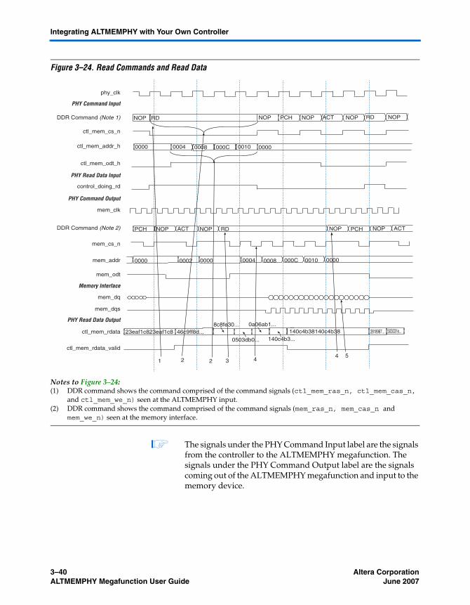
3–40 Altera CorporationALTMEMPHY Megafunction User Guide June 2007
Integrating ALTMEMPHY with Your Own Controller
Figure 3–24. Read Commands and Read Data
Notes to Figure 3–24:(1) DDR command shows the command comprised of the command signals (ctl_mem_ras_n, ctl_mem_cas_n,
and ctl_mem_we_n) seen at the ALTMEMPHY input.(2) DDR command shows the command comprised of the command signals (mem_ras_n, mem_cas_n and
mem_we_n) seen at the memory interface.
1 The signals under the PHY Command Input label are the signals from the controller to the ALTMEMPHY megafunction. The signals under the PHY Command Output label are the signals coming out of the ALTMEMPHY megafunction and input to the memory device.
phy_clk
ctl_mem_addr_h
ctl_mem_cs_n
ctl_mem_odt_h
DDR Command (Note 1)
mem_clk
mem_addr
mem_odt
mem_dqs
mem_dq
ctl_mem_rdata
control_doing_rd
ctl_mem_rdata_valid
DDR Command (Note 2)
mem_cs_n
2818967... 503031e...
1 2 45
PHY Command Input
PHY Read Data Input
PHY Command Output
Memory Interface
PHY Read Data Output
2 34
NOP NOP NOP NOPRD RDPCH ACT NOP
0000 0004 0008 000C 0010 0000
PCH NOP NOP NOP NOP ACTPCHRDACT
0000 0000 000C 000000100004 00080002
23eaf1c823eaf1c8 46c9ff8d...8c8fe30...
0503db0...
0a06ab1...
140c4b3...140c4b38140c4b38
Altera Corporation 3–41June 2007 ALTMEMPHY Megafunction User Guide
Specifications
1. Some of the address and command signals generated by the controller are:
■ ctl_mem_addr_h■ ctl_mem_cas_h■ ctl_mem_cs_n_h■ ctl_mem_ras_n_h■ ctl_mem_we_n_h■ ctl_mem_odt_h
Figure 3–24 shows the No Operation (NOP) command followed by a series of five read commands.
2. The controller issues five consecutive read commands with a starting address of 0×0 with increments of four (0000, 0004, 0008, 000c, 0010). This is shown at the top of Figure 3–24 under the PHY Command Input label.
3. The ALTMEMPHY megafunction generates the read command at the memory interface after five-to-seven memory clock (mem_clk) cycles. The address and commands are generated using the negative edge of the memory clock. This is shown in the Figure 3–24 under the PHY Command Output label.
4. The address and commands are of 2T period and the chip select is of 1T period (mem_clk).
5. The data (mem_dq) at the memory interface is presented after three memory clock cycles of read latency. The read latency is equal to the CAS latency. For this example, CAS latency is equal to three.
By default, the read data from the memory bypasses the controller and is sent directly to the user logic. If your controller needs access to the read data after it has been captured, but before it is sent to the user interface (for example, to perform error detection and correction), connect the ctl_mem_rdata and ctl_mem_rdata_valid outputs from ALTMEMPHY to your controller. The controller must delay both ctl_mem_rdata and ctl_mem_rdata_valid signals by the same amount. Connect the read data and valid outputs of your controller to the ctl_rdata and ctl_rdata_valid inputs of the ALTMEMPHY megafunction, which will then be passed straight through to the local_rdata and local_rdata_valid signals.
3–42 Altera CorporationALTMEMPHY Megafunction User Guide June 2007
Integrating ALTMEMPHY with Your Own Controller
Full-Rate Controller
The read operation for a full-rate controller is shown in Figure 3–25. The handshake mechanism remains similar to that of the half-rate controller except for the following differences:
1. 1T versus 2T addressing.
As the burst size is fixed at four on the memory interface, and also the address and command data path is based on 1T addressing, it takes two memory clock cycles to retrieve the data from the memory for each read command, as shown in Figure 3–25. The first memory cycle is the read command and the second memory cycle is the NOP command. Because of this arrangement, you will see a NOP command between the read commands.
2. Assertion of the chip select signal.
The chip select signal is asserted along with the read command because of the 1T addressing.
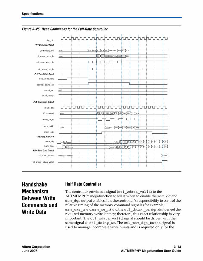
Altera Corporation 3–43June 2007 ALTMEMPHY Megafunction User Guide
Specifications
Figure 3–25. Read Commands for the Full-Rate Controller
Handshake Mechanism Between Write Commands and Write Data
Half Rate Controller
The controller provides a signal (ctl_wdata_valid) to the ALTMEMPHY megafunction to tell it when to enable the mem_dq and mem_dqs output enables. It is the controller’s responsibility to control the relative timing of the memory command signals (for example, mem_cas_n and mem_we_n) and the ctl_doing_wr signals, to meet the required memory write latency; therefore, this exact relationship is very important. The ctl_wdata_valid signal should be driven with the same signal as ctl_doing_wr. The ctl_mem_dqs_burst signal is used to manage incomplete write bursts and is required only for the
phy_clk
ctl_mem_cs_n_h
ctl_mem_addr_h
ctl_mem_odt_h
Command_ctl
mem_clk
mem_addr
mem_odt
mem_dqs
mem_dq
ctl_mem_rdata
local_read_req
ctl_mem_rdata_valid
Command
mem_cs_n
PHY Command Input
PHY Read Data Input
PHY Command Output
Memory Interface
PHY Read Data Output
NOP RD NOP
control_doing_rd
count_wr
local_ready
RD NOP RD NOP RD NOP RD NOP
0000 0004 0000 0008 0000 000c 0000 0010 0000
0000
NOP RD NOP RD NOP RD NOP RD NOP
00040000 0000 0008 0000 000c 0000
NOP RD
0010 0000
e... 8... 000000 1... 4... 3... 7... 0... f... 0... 0... c... 0... 1... 3... 2... 7... e... 8...
00000... 0000 1... 0... 1... 1... 0... 1... 0... 0... 1... 0... 0... 1... 0... 1... 1... 0...
808bdae4ec55833a 473d 8

3–44 Altera CorporationALTMEMPHY Megafunction User Guide June 2007
Handshake Mechanism Between Write Commands and Write Data
full-rate version of the ALTMEMPHY megafunction as the half-rate DDR/DDR2 High-Performance Controller does not support incomplete burst transactions.
Figure 3–26. Write Commands and Write Data
Notes to Figure 3–26:(1) DDR command shows the command comprised of the command signals (ctl_mem_ras_n, ctl_mem_cas_n,
and ctl_mem_we_n) seen at the ALTMEMPHY input.(2) DDR command shows the command comprised of the command signals (mem_ras_n, mem_cas_n, and
mem_we_n) seen at the memory interface.
DDR Command (Note 1)
phy_clk
ctl_mem_addr_h
ctl_mem_cs_n_h
ctl_mem_odt_h
mem_addr
mem_cs_n
mem_odt
mem_dq
control_wdata_valid
control_doing_wr
control_wdata
0000 0003 0000 0004 0008 000C 0010 0000
mem_dqs[1]
PHY Command Input
PHY Write Data Input
PHY Command Output
PHY Write Data Output
12
33
46 7
DDR Command (Note 2) NOP PCH NOP ACT NOP WR ACT NOP
5 5
mem_clk
ACT ACTNOP NOPWR WR
0003 0000 0004 0008 000C 0010 0000 0004 0008
cdb042d1cc72ad13
877d84bf...
13a1563...
26e92ac...
4ccf5491...
9883a83fb8e6045a
2d1b4d7...
5a369af...
Altera Corporation 3–45June 2007 ALTMEMPHY Megafunction User Guide
Specifications
Figure 3–26 shows the sequence of operations that happen during the write transactions. The write operation is explained step-by-step below. All the inputs to the ALTMEMPHY megafunction from the controller should be generated using phy_clk.
1 The signals under the PHY command input label are the signals from the controller to the ALTMEMPHY megafunction and the signals under the PHY command output label are the signals coming out of the ALTMEMPHY megafunction and input to the memory device.
1. Some of the address and command signals generated by the controller are:
■ ctl_mem_addr_h■ ctl_mem_cas_n_h■ ctl_mem_cs_n_h■ ctl_mem_ras_n_h■ ctl_mem_we_n_h■ ctl_mem_odt_h
As can be seen in the waveform (Figure 3–26), the sequence of commands are PreCharge (PCH), Active (ACT), and No Operation (NOP), followed by a series of write commands.
2. The controller puts the five consecutive write commands with a starting address of 0 × with increments of four (0000, 0004, 0008, 000c, 0010). This is shown at the top of Figure 3–26 under the PHY Command Input label.
3. The controller generates the following signals two clock cycles after the write command: control_doing_wr and control_wdata_valid, and must supply the data control_wdata along with these two signals. Refer to Figure 3–26 under the PHY Write Data Input label.
4. The ALTMEMPHY megafunction generates the write command at the memory interface after five-to-seven memory clock (mem_clk) cycles (to accommodate the write delay). The address and commands are generated using the negative edge of the memory clock. This is shown in Figure 3–24 under the PHY Command Output label.
5. The address and commands are of 2T period and the chip select is of 1T period.
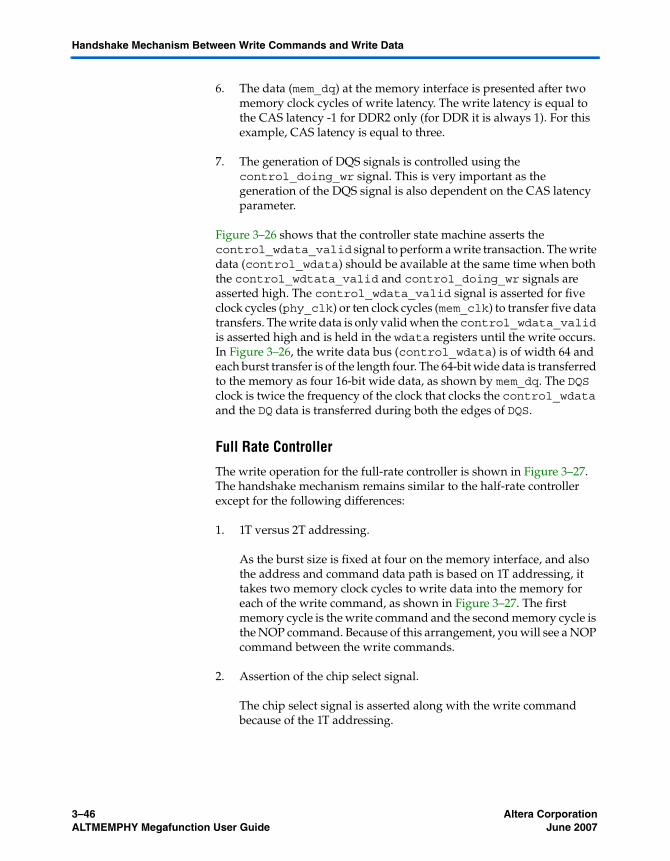
3–46 Altera CorporationALTMEMPHY Megafunction User Guide June 2007
Handshake Mechanism Between Write Commands and Write Data
6. The data (mem_dq) at the memory interface is presented after two memory clock cycles of write latency. The write latency is equal to the CAS latency -1 for DDR2 only (for DDR it is always 1). For this example, CAS latency is equal to three.
7. The generation of DQS signals is controlled using the control_doing_wr signal. This is very important as the generation of the DQS signal is also dependent on the CAS latency parameter.
Figure 3–26 shows that the controller state machine asserts the control_wdata_valid signal to perform a write transaction. The write data (control_wdata) should be available at the same time when both the control_wdtata_valid and control_doing_wr signals are asserted high. The control_wdata_valid signal is asserted for five clock cycles (phy_clk) or ten clock cycles (mem_clk) to transfer five data transfers. The write data is only valid when the control_wdata_valid is asserted high and is held in the wdata registers until the write occurs. In Figure 3–26, the write data bus (control_wdata) is of width 64 and each burst transfer is of the length four. The 64-bit wide data is transferred to the memory as four 16-bit wide data, as shown by mem_dq. The DQS clock is twice the frequency of the clock that clocks the control_wdata and the DQ data is transferred during both the edges of DQS.
Full Rate Controller
The write operation for the full-rate controller is shown in Figure 3–27. The handshake mechanism remains similar to the half-rate controller except for the following differences:
1. 1T versus 2T addressing.
As the burst size is fixed at four on the memory interface, and also the address and command data path is based on 1T addressing, it takes two memory clock cycles to write data into the memory for each of the write command, as shown in Figure 3–27. The first memory cycle is the write command and the second memory cycle is the NOP command. Because of this arrangement, you will see a NOP command between the write commands.
2. Assertion of the chip select signal.
The chip select signal is asserted along with the write command because of the 1T addressing.
Altera Corporation 3–47June 2007 ALTMEMPHY Megafunction User Guide
Specifications
3. In order to support full-rate, the ALTMEMPHY megafunction has an extra control signal (ctl_mem_dqs_burst) that the controller must provide in addition to ctl_mem_doing_wr. In full-rate mode, the PHY allows separates control of the DQ and DQS output enables in order to support incomplete bursts. For example, if the memory burst length is four and the local side burst length is two, you may ask for a write of length one. In order to support this, the controller must be able to enable the DQS outputs for the full memory burst length (two clock cycles, four DQS edges) while only enabling the DQ outputs for the number of cycles that you requested (one clock cycle, two beats of data).
1 The ctl_mem_dqs_burst signal is asserted one cycle after the assertion of the control_doing_wr signal.
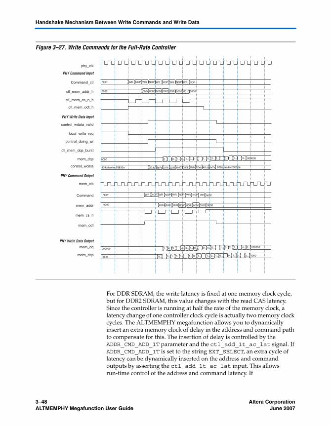
3–48 Altera CorporationALTMEMPHY Megafunction User Guide June 2007
Handshake Mechanism Between Write Commands and Write Data
Figure 3–27. Write Commands for the Full-Rate Controller
For DDR SDRAM, the write latency is fixed at one memory clock cycle, but for DDR2 SDRAM, this value changes with the read CAS latency. Since the controller is running at half the rate of the memory clock, a latency change of one controller clock cycle is actually two memory clock cycles. The ALTMEMPHY megafunction allows you to dynamically insert an extra memory clock of delay in the address and command path to compensate for this. The insertion of delay is controlled by the ADDR_CMD_ADD_1T parameter and the ctl_add_1t_ac_lat signal. If ADDR_CMD_ADD_1T is set to the string EXT_SELECT, an extra cycle of latency can be dynamically inserted on the address and command outputs by asserting the ctl_add_1t_ac_lat input. This allows run-time control of the address and command latency. If
phy_clk
ctl_mem_cs_n_h
ctl_mem_addr_h
ctl_mem_odt_h
Command_ctl
mem_clk
mem_addr
mem_odt
mem_dqs
mem_dq
control_wdata_valid
Command
mem_cs_n
PHY Command Input
PHY Write Data Input
PHY Command Output
NOP WR NOP
local_write_req
control_doing_wr
ctl_mem_dqs_burst
WR NOP WR NOP WR NOP
0000 0008 0000 000c 0000 0010 0000
NOP WR NOP WR NOP WR NOP WR NOP
00040000 0000 0008 0000 000c 0000
NOP WR
0010 0000
000000 1... 4... 3... 7... 0... f... 0... 0... c... 0... 1... 3... 2... 7... e... 8... 000000
0000 0... 0... 1... 0... 1... 1... 0... 1... 1... 0... 1... 0... 0... 1... 0000
PHY Write Data Output
mem_dqs
control_wdata
WR NOP
0004 0000
0000 0... 0... 0... 1... 1... 1... 0... 1... 0... 1... 0... 0... 000000
808bdae4ec55833a 8e7a
1... 0... 0...
473d 02f501f4 08f304f7 20eb10fb 8e7a40cb 808bdae4ec55833a
0... 0...
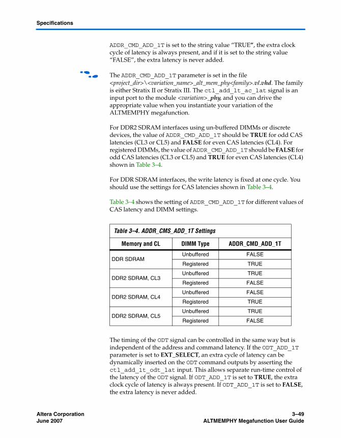
Altera Corporation 3–49June 2007 ALTMEMPHY Megafunction User Guide
Specifications
ADDR_CMD_ADD_1T is set to the string value “TRUE”, the extra clock cycle of latency is always present, and if it is set to the string value “FALSE”, the extra latency is never added.
f The ADDR_CMD_ADD_1T parameter is set in the file <project_dir>\<variation_name>_alt_mem_phy<family>.v/.vhd. The family is either Stratix II or Stratix III. The ctl_add_lt_ac_lat signal is an input port to the module <variation>_phy, and you can drive the appropriate value when you instantiate your variation of the ALTMEMPHY megafunction.
For DDR2 SDRAM interfaces using un-buffered DIMMs or discrete devices, the value of ADDR_CMD_ADD_1T should be TRUE for odd CAS latencies (CL3 or CL5) and FALSE for even CAS latencies (CL4). For registered DIMMs, the value of ADDR_CMD_ADD_1T should be FALSE for odd CAS latencies (CL3 or CL5) and TRUE for even CAS latencies (CL4) shown in Table 3–4.
For DDR SDRAM interfaces, the write latency is fixed at one cycle. You should use the settings for CAS latencies shown in Table 3–4.
Table 3–4 shows the setting of ADDR_CMD_ADD_1T for different values of CAS latency and DIMM settings.
The timing of the ODT signal can be controlled in the same way but is independent of the address and command latency. If the ODT_ADD_1T parameter is set to EXT_SELECT, an extra cycle of latency can be dynamically inserted on the ODT command outputs by asserting the ctl_add_1t_odt_lat input. This allows separate run-time control of the latency of the ODT signal. If ODT_ADD_1T is set to TRUE, the extra clock cycle of latency is always present. If ODT_ADD_1T is set to FALSE, the extra latency is never added.
Table 3–4. ADDR_CMS_ADD_1T Settings
Memory and CL DIMM Type ADDR_CMD_ADD_1T
DDR SDRAMUnbuffered FALSE
Registered TRUE
DDR2 SDRAM, CL3Unbuffered TRUE
Registered FALSE
DDR2 SDRAM, CL4Unbuffered FALSE
Registered TRUE
DDR2 SDRAM, CL5Unbuffered TRUE
Registered FALSE

3–50 Altera CorporationALTMEMPHY Megafunction User Guide June 2007
Handshake Mechanism Between Write Commands and Write Data
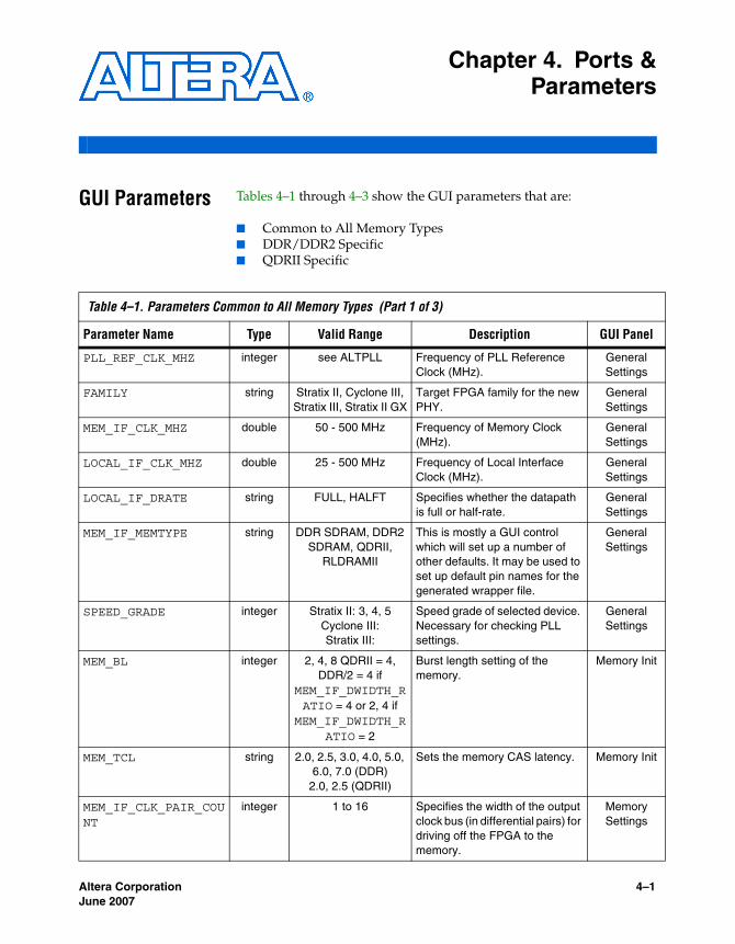
Altera Corporation 4–1June 2007
Chapter 4. Ports &Parameters
GUI Parameters Tables 4–1 through 4–3 show the GUI parameters that are:
■ Common to All Memory Types■ DDR/DDR2 Specific■ QDRII Specific
Table 4–1. Parameters Common to All Memory Types (Part 1 of 3)
Parameter Name Type Valid Range Description GUI Panel
PLL_REF_CLK_MHZ integer see ALTPLL Frequency of PLL Reference Clock (MHz).
General Settings
FAMILY string Stratix II, Cyclone III, Stratix III, Stratix II GX
Target FPGA family for the new PHY.
General Settings
MEM_IF_CLK_MHZ double 50 - 500 MHz Frequency of Memory Clock (MHz).
General Settings
LOCAL_IF_CLK_MHZ double 25 - 500 MHz Frequency of Local Interface Clock (MHz).
General Settings
LOCAL_IF_DRATE string FULL, HALFT Specifies whether the datapath is full or half-rate.
General Settings
MEM_IF_MEMTYPE string DDR SDRAM, DDR2 SDRAM, QDRII,
RLDRAMII
This is mostly a GUI control which will set up a number of other defaults. It may be used to set up default pin names for the generated wrapper file.
General Settings
SPEED_GRADE integer Stratix II: 3, 4, 5Cyclone III:Stratix III:
Speed grade of selected device. Necessary for checking PLL settings.
General Settings
MEM_BL integer 2, 4, 8 QDRII = 4, DDR/2 = 4 if
MEM_IF_DWIDTH_RATIO = 4 or 2, 4 if
MEM_IF_DWIDTH_RATIO = 2
Burst length setting of the memory.
Memory Init
MEM_TCL string 2.0, 2.5, 3.0, 4.0, 5.0, 6.0, 7.0 (DDR)
2.0, 2.5 (QDRII)
Sets the memory CAS latency. Memory Init
MEM_IF_CLK_PAIR_COUNT
integer 1 to 16 Specifies the width of the output clock bus (in differential pairs) for driving off the FPGA to the memory.
Memory Settings
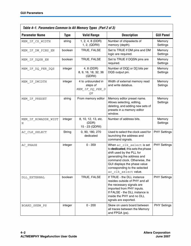
4–2 Altera CorporationALTMEMPHY Megafunction User Guide June 2007
GUI Parameters
MEM_IF_CS_WIDTH string 1, 2, 4, 8 (DDR)1, 2, (QDRII)
Number of chipselects of memory (depth).
Memory Settings
MEM_IF_DM_PINS_EN boolean TRUE, FALSE Set to TRUE if DM pins and DM logic are required.
Memory Settings
MEM_IF_DQSN_EN boolean TRUE, FALSE Set to TRUE if DQSN pins are required.
Memory Settings
MEM_IF_DQ_PER_DQS integer 4, 8 (DDR)8, 9, 16, 18, 32, 36
(QDRII)
Number of DQ[] or D[] bits per DQS output pin.
Memory Settings
MEM_IF_DWIDTH integer 4 to unbounded in steps of
MEM_IF_DQ_PER_DQS
Width of external memory read and write databus.
Memory Setings
MEM_IF_PRESET string From memory editor Memory editor preset name. Allows selecting, editing, deleting, and adding new sets of presets in a memory editor window.
Memory Settings
MEM_IF_ROWADDR_WIDTH
integer 8, 10, 12, 13, etc. (DDR)
15 - 23 (QDRII)
Number of address bits. Memory Settings
AC_CLK_SELECT String 0, 90, 180, 270 dedicated
Used to select the clock used for launching the address and command signals.
PHY Settings
AC_PHASE integer 0 - 359 When ac_clk_select is set to dedicated, this sets the phase shift used by the PLL for generating the address and command clock. Otherwise, the GUI displays the phase value corresponding to the selected ac_clk_select value.
PHY Settings
DLL_EXTERNAL boolean TRUE, FALSE If TRUE - the DLL instance resides outside of PHY and all the necessary signals are imported from PHY inputs.If FALSE - the DLL instance is inside the PHY and no DLL sgnals are exported.
PHY Settings
BOARD_SKEW_PS integer 0 - 200 Skew on users board between all traces between the Memory and FPGA (ps).
PHY Setings
Table 4–1. Parameters Common to All Memory Types (Part 2 of 3)
Parameter Name Type Valid Range Description GUI Panel

Altera Corporation 4–3June 2007 ALTMEMPHY Megafunction User Guide
Ports & Parameters
DEDICATED_MEMORY_CLK_EN
boolean FALSE If TRUE, the memory clock uses a dedicated PLL output. If FALSE, the memory clock uses the DDIO output.
PHY Setings
FAST_SIMULATION_EN boolean TRUE, FALSE May be used to calibrate using just one DQ pin. It enables faster simulation of the calibration sequence.
PHY Settings
DLL_EXTERNAL boolean TRUE, FALSE If TRUE, the DLL is not instanced internally in the PHY and must be connected up externally. The dqs_delay_ctrl_import and the dll_reference_clk signals must then be connected up to a DLL instance.
PHY Settings
PLL_RECONFIG_PORTS_EN
boolean TRUE, FALSE If TRUE, the multiplexor to the PLL reconfig block shall be switched, dependant upon the pll_reconfig_enable input.
PHY Settings
Table 4–1. Parameters Common to All Memory Types (Part 3 of 3)
Parameter Name Type Valid Range Description GUI Panel
Table 4–2. Parameters that are DDR/DDR2 Specific (Part 1 of 3)
Parameter Name Type Valid Range Description GUI Panel
ENABLE_ECC boolean TRUE, FALSE Enables ECC functionality. Local Interface
LOCAL_IF_TYPE_AVALON
string TRUE, FALSE Boolean flag specifying if the interface is Avalon or not.
Local Interface
LOCAL_IF_BURST_LENGTH
integer 1, 2, 4 The burst length of the Avalon interface.
Memory Init
MEM_BTYPE string Sequential or interleaved
Sets the memory burst order of the memory.
Memory Init
MEM_DLL_EN string Yes or No Enables the DLL in the memory device.
Memory Init
MEM_DRV_STR string Normal or reduced Sets the memory drive strength Memory Init
MEM_ODT string Disabled, 50, 75, and 150
Sets the memory ODT value. Memory Init
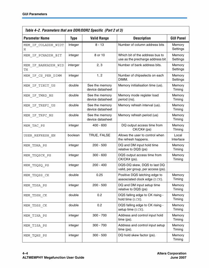
4–4 Altera CorporationALTMEMPHY Megafunction User Guide June 2007
GUI Parameters
MEM_IF_COLADDR_WIDTH
Integer 8 - 13 Number of column address bits Memory Settings
MEM_IF_PCHADDR_BIT integer 8 or 10 Which bit of the address bus to use as the precharge address bit
Memory Settings
MEM_IF_BANKADDR_WIDTH
interger 2, 3 Number of bank address bits. Memory Settings
MEM_IF_CS_PER_DIMM integer 1, 2 Number of chipselects on each DIMM.
Memory Settings
MEM_IF_TINIT_US double See the memory device datasheet
Memory initialisation time (us). Memory Timing
MEM_IF_TMRD_NS double See the memory device datasheet
Memory mode register load period (ns).
Memory Timing
MEM_IF_TREFI_US double See the memory device datasheet
Memory refresh interval (us). Memory Timing
MEM_IF_TRFC_NS double See the memory device datasheet
Memory refresh period (us) Memory Timing
MEM_TAC_PS integer 400 - 600 DQ output access time from CK/CK# (ps)
Memory TIming
USER_REFRESH_EN boolean TRUE, FALSE Allows the user to control when the refresh happens.
Local Interface
MEM_TDHA_PS integer 200 - 500 DQ and DM input hold time relative to DQS (ps)
Memory Timing
MEM_TDQSCK_PS integer 300 - 600 DQS output access time from CK/CK# (ps).
Memory Timing
MEM_TDQSQ_PS integer 200 - 400 DQS-DQ skew, DQS to last DQ valid, per group, per access (ps).
MEM_TDQSS_CK double 0.25 Positive DQS latching edge to assosciated clock edge (tCK).
Memory Timing
MEM_TDSA_PS integer 200 - 500 DQ and DM input setup time relative to DQS (ps)
Memory Timing
MEM_TDSH_CK double 0.2 DQS falling edge to CK rising - hold time (tCK).
Memory Timing
MEM_TDSS_CK double 0.2 DQS falling edge to CK rising - setup time (tCK).
Memory Timing
MEM_TIHA_PS integer 300 - 700 Address and control input hold time (ps).
Memory Timing
MEM_TISA_PS integer 300 - 700 Address and control input setup time (ps).
Memory Timing
MEM_TQHS_PS integer 300 - 500 DQ hold skew factor (ps). Memory Timing
Table 4–2. Parameters that are DDR/DDR2 Specific (Part 2 of 3)
Parameter Name Type Valid Range Description GUI Panel
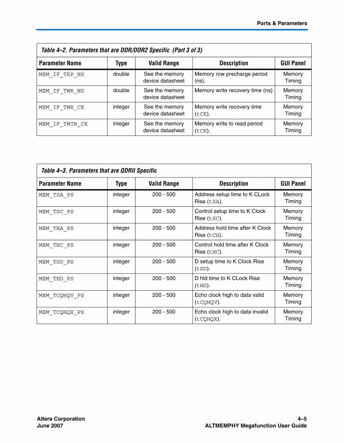
Altera Corporation 4–5June 2007 ALTMEMPHY Megafunction User Guide
Ports & Parameters
MEM_IF_TRP_NS double See the memory device datasheet
Memory row precharge period (ns).
Memory Timing
MEM_IF_TWR_NS double See the memory device datasheet
Memory write recovery time (ns) Memory Timing
MEM_IF_TWR_CK integer See the memory device datasheet
Memory write recovery time (tCK).
Memory Timing
MEM_IF_TWTR_CK integer See the memory device datasheet
Memory write to read period (tCK).
Memory Timing
Table 4–2. Parameters that are DDR/DDR2 Specific (Part 3 of 3)
Parameter Name Type Valid Range Description GUI Panel
Table 4–3. Parameters that are QDRII Specific
Parameter Name Type Valid Range Description GUI Panel
MEM_TSA_PS integer 200 - 500 Address setup time to K CLock Rise (tSA).
Memory Timing
MEM_TSC_PS integer 200 - 500 Control setup time to K Clock Rise (tSC).
Memory Timing
MEM_THA_PS integer 200 - 500 Address hold time after K Clock Rise (tCH).
Memory Timing
MEM_THC_PS integer 200 - 500 Control hold time after K Clock Rise (tHC).
Memory Timing
MEM_TSD_PS integer 200 - 500 D setup time to K Clock Rise (tSD).
Memory Timing
MEM_THD_PS integer 200 - 500 D hld time to K CLock Rise (tHD).
Memory Timing
MEM_TCQHQV_PS integer 200 - 500 Echo clock high to data valid (tCQHQV).
Memory Timing
MEM_TCQHQX_PS integer 200 - 500 Echo clock high to data invalid (tCQHQX).
Memory Timing

4–6 Altera CorporationALTMEMPHY Megafunction User Guide June 2007
DDR/DDR2/ DDR3 Port Lists
DDR/DDR2/DDR3 Port Lists
Tables 4–4 through 4–11 show the DDR/DDR2 port list parameters for:
■ Clocking■ PLL Reconfiguration Interface (Optional - for Stratix II Series Only)■ External DLL Interface (Optional - for Stratix II Series Only)■ Interface to the Memory Controller■ User Interface for the Controller■ Datapath Interface for the Controller■ I/O Interface to the External Memory Device■ ALTMEMPHY Calibration Status Interface
Table 4–4. Port Lists (Clocking)
Signal Name Type Width Description
global_reset_n input 1 The asynchronous reset input to the controller. All other reset signals are derived from resynchronized versions of this. This signal holds the complete ALTMEMPHY, including the PLL, in reset while low.
soft_reset_n input 1 The asynchronous reset input to reset controller. This reset causes the PHY to pulse the reset to the PLL on detection of a falling edge, and holds the rest if the ALTMEMPHY in reset while the signal is low.
phy_clk output 1 The ALTMEMPHY clock provided to the user. All user inputs and outputs to the ALTMEMPHY are synchronous to this clock.
pll_ref_clk input 1 The reference clock input to PLL.
reset_phy_clk_n output 1 Asynchronous Reset - asserted asynchronously and de-asserted synchronously to associated clock domain.
reset_request_n output 1 Reset request output that indicates when the PLL outputs are not locked. Use this as a reset request input to any system-level reset controller you may have. Note that this signal is always low while the PLL is locking, and so any reset logic using it is advised to detect a reset request on a falling-edge rather than by level detection.

Altera Corporation 4–7June 2007 ALTMEMPHY Megafunction User Guide
Ports & Parameters
Table 4–5. Port Lists (PLL Reconfiguration Interface – Optional, for Stratix II Series Only)
Signal Name Type Width Description
pll_reconfig_enable input 1 Allows access to the PLL Reconfig block. Hold this signal low in normal operation. While the ALTMEMPHY is held in reset (via the soft_reset_n signal), and the reset_request_n signal is 1, it is safe to reconfigure the PLL. To reconfigure the PLL, set this signal to 1 and use the other pll_reconfig signals to access the PLL. When finished reconfiguring, set this signal to 0, and then set the soft_reset_n signal to 1 to bring the ALTMEMPHY out of reset. Note that for this signal to work, the PLL_RECONFIG_PORTS_EN GUI parameter must be set to true.
pll_reconfig_write_param
input 9 See the ALTPLL_RECONFIG User Guide for more information.
pll_reconfig_read_param
input 9 See the ALTPLL_RECONFIG User Guide for more information.
pll_reconfig input 1 See the ALTPLL_RECONFIG User Guide for more information.
pll_reconfig_counter_type
input 4 See the ALTPLL_RECONFIG User Guide for more information.
pll_reconfig_counter_param
input 3 See the ALTPLL_RECONFIG User Guide for more information.
pll_reconfig_data_in
input 9 See the ALTPLL_RECONFIG User Guide for more information.
pll_reconfig_busy output 1 See the ALTPLL_RECONFIG User Guide for more information.
pll_reconfig_data_out
output 9 See the ALTPLL_RECONFIG User Guide for more information.
pll_reconfig_clk output 1 Synchronous clock to use for any logic accessing the pll_reconfig interface.
pll_reconfig_reset output 1 Synchronous clock to use for any logic accessing the pll_reconfig interface.

4–8 Altera CorporationALTMEMPHY Megafunction User Guide June 2007
DDR/DDR2/ DDR3 Port Lists
Table 4–6. Port Lists (External DLL Interface – Optional, for Stratix II Series Only)
Signal Name Type Width Description
dqs_delay_ctrl_export
output 6 Allows sharing DLL in this ALTMEMPHY instance with another ALTMEMPHY instance. Connect the export port on the ALTMEMPHY instance with a DLL to the import port on the other ALTMEMPHY instance.
dqs_delay_ctrl_import
input 6 Allows the use of DLL in another ALTMEMPHY instance in this ALTMEMPHY instance. Connect the export port on the ALTMEMPHY instance with a DLL to the import port on the other ALTMEMPHY instance.
dll_reference_clk output 1 Reference clock to feed to an externally instantiated DLL.
Table 4–7. Port Lists (Interface to the Memory Controller) Note (1) (Part 1 of 3)
Signal Name Type Width Description
ctl_add_1t_ac_lat input 1 When asserted, one extra address and command clock cycle (1T) of latency is inserted in the address and command path if ADDR_CMD_ADD_1T is set to EXT_SELECT.
ctl_add_intermediate_regs
Input 1 When asserted, an additional intermediate register or registers is included in the address and command path if ADDR_CMD_ADD_INTERMEDIATE_REGS is set to EXT_SELECT. When the GUI generates an ALTMEMPHY, this signal is automatically set to meet core timing requirements, dependant upon the AC_PHASE being used.
ctl_address output LOCAL_IF_AWIDTH
The address corresponding to a write or read request.
ctl_be output LOCAL_IF_DWIDTH/8
The output to the controller indicating the byte-enable flags.
ctl_doing_rd input 1 The active-high signal from the controller specifying that a read command has been issued to the external RAM.
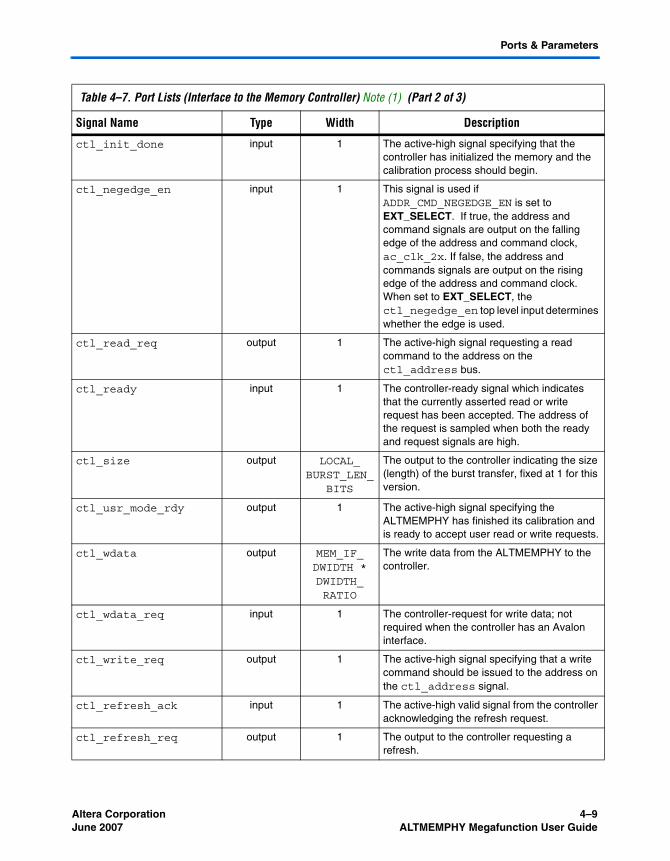
Altera Corporation 4–9June 2007 ALTMEMPHY Megafunction User Guide
Ports & Parameters
ctl_init_done input 1 The active-high signal specifying that the controller has initialized the memory and the calibration process should begin.
ctl_negedge_en input 1 This signal is used if ADDR_CMD_NEGEDGE_EN is set to EXT_SELECT. If true, the address and command signals are output on the falling edge of the address and command clock, ac_clk_2x. If false, the address and commands signals are output on the rising edge of the address and command clock. When set to EXT_SELECT, the ctl_negedge_en top level input determines whether the edge is used.
ctl_read_req output 1 The active-high signal requesting a read command to the address on the ctl_address bus.
ctl_ready input 1 The controller-ready signal which indicates that the currently asserted read or write request has been accepted. The address of the request is sampled when both the ready and request signals are high.
ctl_size output LOCAL_BURST_LEN_
BITS
The output to the controller indicating the size (length) of the burst transfer, fixed at 1 for this version.
ctl_usr_mode_rdy output 1 The active-high signal specifying the ALTMEMPHY has finished its calibration and is ready to accept user read or write requests.
ctl_wdata output MEM_IF_DWIDTH * DWIDTH_RATIO
The write data from the ALTMEMPHY to the controller.
ctl_wdata_req input 1 The controller-request for write data; not required when the controller has an Avalon interface.
ctl_write_req output 1 The active-high signal specifying that a write command should be issued to the address on the ctl_address signal.
ctl_refresh_ack input 1 The active-high valid signal from the controller acknowledging the refresh request.
ctl_refresh_req output 1 The output to the controller requesting a refresh.
Table 4–7. Port Lists (Interface to the Memory Controller) Note (1) (Part 2 of 3)
Signal Name Type Width Description

4–10 Altera CorporationALTMEMPHY Megafunction User Guide June 2007
DDR/DDR2/ DDR3 Port Lists
ctl_burstbegin output 1 The output to the controller indicating the start of a burst.
ctl_rdata input MEM_IF_DWIDTH * DWIDTH_RATIO
The read data from the controller.
ctl_rdata_valid input 1 The active-high valid signal for the controller read data.
ctl_add_1t_odt_lat input 1 When asserted one extra address and command clock cycle (1T) of latency is inserted in the address and command ODT path if ODT_ADD_1T is set to EXT_SELECT.
Note to Table 4–7:(1) Interface signals to the controller either through the sequencer or user interface.
Table 4–7. Port Lists (Interface to the Memory Controller) Note (1) (Part 3 of 3)
Signal Name Type Width Description
Table 4–8. Port Lists (User Interface for the Controller) (Part 1 of 2) Note (1),
Signal Name Type Width Description
local_address input LOCAL_IF_AWIDTH
The address corresponding to a write or read request.
local_be input LOCAL_IF_DWIDTH / 8
The input to ALTMEMPHY indicating the byte-enable flags.
local_read_req input 1 The active-high signal requesting a read command to the address on the ctl_address bus.
local_ready output 1 The controller-ready signal which indicates that the currently asserted read or write request has been accepted. The address of the request is sampled when both the ready and request signals are high.
local_size input LOCAL_BURST_LEN_
BITS
The output to the controller indicating the size (length) of the burst transfer, fixed at 1 for this version.
local_wdata input LOCAL_IF_DWIDTH
The write data from the user to/from the ALTMEMPHY megafunction.
local_wdata_req output 1 The controller request for write data; not required when the controller has an Avalon interface.
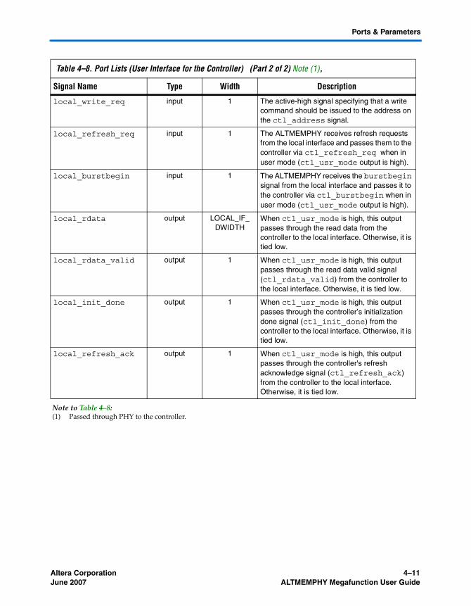
Altera Corporation 4–11June 2007 ALTMEMPHY Megafunction User Guide
Ports & Parameters
local_write_req input 1 The active-high signal specifying that a write command should be issued to the address on the ctl_address signal.
local_refresh_req input 1 The ALTMEMPHY receives refresh requests from the local interface and passes them to the controller via ctl_refresh_req when in user mode (ctl_usr_mode output is high).
local_burstbegin input 1 The ALTMEMPHY receives the burstbegin signal from the local interface and passes it to the controller via ctl_burstbegin when in user mode (ctl_usr_mode output is high).
local_rdata output LOCAL_IF_DWIDTH
When ctl_usr_mode is high, this output passes through the read data from the controller to the local interface. Otherwise, it is tied low.
local_rdata_valid output 1 When ctl_usr_mode is high, this output passes through the read data valid signal (ctl_rdata_valid) from the controller to the local interface. Otherwise, it is tied low.
local_init_done output 1 When ctl_usr_mode is high, this output passes through the controller’s initialization done signal (ctl_init_done) from the controller to the local interface. Otherwise, it is tied low.
local_refresh_ack output 1 When ctl_usr_mode is high, this output passes through the controller's refresh acknowledge signal (ctl_refresh_ack) from the controller to the local interface. Otherwise, it is tied low.
Note to Table 4–8:(1) Passed through PHY to the controller.
Table 4–8. Port Lists (User Interface for the Controller) (Part 2 of 2) Note (1),
Signal Name Type Width Description

4–12 Altera CorporationALTMEMPHY Megafunction User Guide June 2007
DDR/DDR2/ DDR3 Port Lists
Table 4–9. Port Lists (Datapath Interface for the Controller – address/cmd and wdata/rdata) (Part 1 of 2) Note (1), (2)
Signal Name Type Width Description
ctl_mem_addr_h input MEM_IF_ROWADDR_WIDTH
The row or column address which is sent to the external memory.
ctl_mem_addr_l input MEM_IF_ROWADDR_WIDTH
The row or column address which is sent to the external memory.
ctl_mem_ba_h input MEM_IF_BANKADDR_
WIDTH
The bank address which is sent to the external memory.
ctl_mem_ba_l input MEM_IF_BANKADDR_
WIDTH
The bank address which is sent to the external memory.
ctl_mem_be input MEM_IF_DM_WIDTH /
8
The optional byte-enable signals for the write data to the external memory. The ALTMEMPHY megafunction converts the byte enables into memory mem_dm signals. If mem_dm pins are not required (mem_dm_pins set to FALSE), the mem_dm logic is not generated and the mem_dm pins are not instantiated.
ctl_mem_cas_n_h input 1 The column-address strobe signal from the controller to the memory.
ctl_mem_cas_n_l input 1 The column-address strobe signal from the controller to the memory.
ctl_mem_cke_h input MEM_IF_CS_WIDTH
The clock-enable signal from the controller to the memory.
ctl_mem_cke_l input MEM_IF_CS_WIDTH
The clock-enable signal from the controller to the memory.
ctl_mem_cs_n_h input MEM_IF_CS_WIDTH
The chip-select signal from the controller to the memory.
ctl_mem_cs_n_l input MEM_IF_CS_WIDTH
The chip select signal from the controller to the memory.
ctl_mem_dqs_burst input 1 Controls the DQS output enables of the DQS pins. See the ALTMEMPHY User Guide for specific details of the timing of this signal.
ctl_mem_odt_h input MEM_IF_CS_WIDTH
The on-die termination signal from the controller to the memory.
ctl_mem_odt_l input MEM_IF_CS_WIDTH
The on-die termination signal from the controller to the memory.
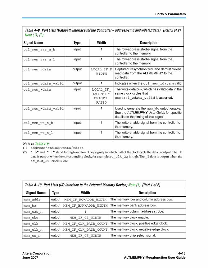
Altera Corporation 4–13June 2007 ALTMEMPHY Megafunction User Guide
Ports & Parameters
ctl_mem_ras_n_h input 1 The row-address strobe signal from the controller to the memory.
ctl_mem_ras_n_l input 1 The row-address strobe signal from the controller to the memory.
ctl_mem_rdata output LOCAL_IF_DWIDTH
Captured, resynchronized, and demultiplexed read data from the ALTMEMPHY to the controller.
ctl_mem_rdata_valid output 1 Indicates when the ctl_mem_rdata is valid.
ctl_mem_wdata input LOCAL_IF_DWIDTH * DWIDTH_RATIO
The write data bus, which has valid data in the same clock cycles that control_wdata_valid is asserted.
ctl_mem_wdata_valid input 1 Used to generate the mem_dq output enable. See the ALTMEMPHY User Guide for specific details on the timing of this signal.
ctl_mem_we_n_h input 1 The write-enable signal from the controller to the memory.
ctl_mem_we_n_l input 1 The write-enable signal from the controller to the memory.
Note to Table 4–9:(1) address/cmd and wdata/rdata(2) “_h” and “_l” stand for high and low. They signify in which half of the clock cycle the data is output. The _h
data is output when the corresponding clock, for example ac_clk_2x is high. The _l data is output when the ac_clk_2x clock is low.
Table 4–9. Port Lists (Datapath Interface for the Controller – address/cmd and wdata/rdata) (Part 2 of 2) Note (1), (2)
Signal Name Type Width Description
Table 4–10. Port Lists (I/O Interface to the External Memory Device) Note (1) (Part 1 of 2)
Signal Name Type Width Description
mem_addr output MEM_IF_ROWADDR_WIDTH The memory row and column address bus.
mem_ba output MEM_IF_BANKADDR_WIDTH The memory bank address bus.
mem_cas_n output 1 The memory column address strobe.
mem_cke output MEM_IF_CS_WIDTH The memory clock enable.
mem_clk output MEM_IF_CLK_PAIR_COUNT The memory clock, positive edge clock.
mem_clk_n output MEM_IF_CLK_PAIR_COUNT The memory clock, negative edge clock.
mem_cs_n output MEM_IF_CS_WIDTH The memory chip select signal.

4–14 Altera CorporationALTMEMPHY Megafunction User Guide June 2007
DDR/DDR2/ DDR3 Port Lists
mem_dm output MEM_IF_DM_WIDTH The optional memory data mask bus.
mem_dq bidi MEM_IF_DWIDTH The memory bidirectional data bus.
mem_dqs bidi MEM_IF_DWIDTH / MEM_IF_DQ_PER_DQS
The memory bidirectional data strobe bus.
mem_dqsn bidi MEM_IF_DWIDTH / MEM_IF_DQ_PER_DQS
The memory bidirectional data strobe bus.
mem_odt output MEM_IF_CS_WIDTH The memory on-die termination control signal.
mem_ras_n output 1 The memory row address strobe.
mem_reset_n output 1 The memory-reset signal.
mem_we_n output 1 The memory write-enable signal.
Note to Table 4–10:(1) Connected to WYSIWYGS/pad atoms.
Table 4–10. Port Lists (I/O Interface to the External Memory Device) Note (1) (Part 2 of 2)
Signal Name Type Width Description
Table 4–11. Port Lists (ALTMEMPHY Calibration Status Interface)
Signal Name Type Width Description
resynchronisation_successful
output 1 Active-high signal that is set to indicate successful calibration of the read data resynchronisation clock phase.
postamble_qsuccessful
output 1 Active-high signal that is set to indicate successful read postamble calibration.
tracking_successful output 1 Active-high signal that is set to indicate successful mimic path VT variation tracking operation.
tracking_adjustment_up
output 1 Active-high signal that is pulsed to indicate that the mimic path tracking has adjusted the resynchronisation clock phasing upwards.
tracking_adjustment_down
output 1 Active-high signal that is pulsed to indicate that the mimic path tracking has adjusted the resynchronisation clock phasing downwards.

Altera Corporation 4–15June 2007 ALTMEMPHY Megafunction User Guide
Ports & Parameters
QDRII Port Lists Tables 4–12 through 4–16 show the QDRII port list parameters for:
■ Clocking■ Interface to Memory Controller■ Datapath Interface for the Controller■ I/O Interface to the External Memory Device■ PHY Calibration Status Interface
Table 4–12. QDRII Port List (Clocking)
Signal Name Type Width Description
global_reset_n input 1 Asynchronous reset input to reset the controller. All other reset signals are derived from resynchronised versions of this. This signal holds the complete PHY including the PLL in reset while low.
reset_request_n output 1 Reset request output that indicates when the PLL outputs are not locked. Use this as a reset request input to any system-level reset controller you may have.
soft_reset_n input 1 Asynchronous reset input to reset the controller. This reset causes the PHY to pulse the reset to the PLL on detection of a falling edge, and it holds the rest if the PHY in reset while the signal is low.
phy_clk output 1 PHY clock provided to the user, all user inputs and outputs are synchronous to this clock.
pll_ref_clk input 1 Reference clock input to PLL.
reset_phy_clk_n output 1 Asynchronous Reset - asserted asynchronously and de-asserted synchronously to associated clock domain.
Table 4–13. QDRII Port List (Interface to the Memory Controller) Note (1)
Signal Name Type Width Description
ctl_usr_mode_rdy output 1 Active high signal specifying the PHY has finished its calibration and is ready to accept user read or write requests.
Note to Table 4–13:(1) Calibration control or passed through from the user interface.

4–16 Altera CorporationALTMEMPHY Megafunction User Guide June 2007
QDRII Port Lists
Table 4–14. QDRII Port List (Datapath Interface for the Controller) Note (1)
Signal Name Type Width Description
ctl_mem_addr_h input MEM_IF_ROWADDR_WIDTH
Write address from the controller to the external memory.
ctl_mem_addr_l input MEM_IF_ROWADDR_WIDTH
Read address from the controller to the external memory.
ctl_mem_be input LOCAL_IF_DWIDTH / 8
Optional byte enable signals for the write data to the external memory. The PHY converts the byte enables into memory DM signals. If DM pins are not required (MEM_DM_PINS set to false), the DM logic is not generated and the DM pins are not instantiated.
ctl_mem_rdata output LOCAL_IF_DWIDTH
Captured, resynchronised, and de-multiplexed read data from the PHY to the controller.
ctl_mem_rdata_valid output 1 Indicates when the ctl_mem_rdata is valid.
ctl_mem_wdata input MEM_IF_DWIDTH *
DWIDTH_RATIO
The write databus, which has valid data in the same clock cycles that control_wdata_valid is asserted.
ctl_mem_wdata_valid input 1 Used to generate the DQ output enable. See the ALTMEMPHY User Guide for specific details on the timing of this signal.
ctl_mem_wps_n input 1 Write enable signal from the controller to the memory (QDRII). When this signal is asserted, a write request is issued to the address presented on the ctl_mem_addr_h port.
ctl_mem_rps_n input 1 Read enable signal from the controller to the memory (QDRII). When this signal is asserted, a read request is issued to the address presented on the ctl_mem_addr_l port.
Note to Table 4–14:(1) Address and command and wdata/rdata.
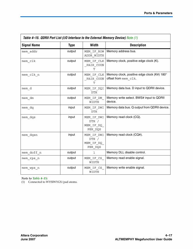
Altera Corporation 4–17June 2007 ALTMEMPHY Megafunction User Guide
Ports & Parameters
Table 4–15. QDRII Port List (I/O Interface to the External Memory Device) Note (1)
Signal Name Type Width Description
mem_addr output MEM_IF_ROWADDR_WIDTH
Memory address bus.
mem_clk output MEM_IF_CLK_PAIR_COUN
T
Memory clock, positive edge clock (K).
mem_clk_n output MEM_IF_CLK_PAIR_COUN
T
Memory clock, positive edge clock (K#) 180° offset from mem_clk.
mem_d output MEM_IF_DQIDTH
Memory data bus. D input to QDRII device.
mem_dm output MEM_IF_DM_WIDTH
Memory write select. BWS# input to QDRII device.
mem_dq input MEM_IF_DWIDTH
Memory data bus. Q output from QDRII device.
mem_dqs input MEM_IF_DWIDTH /
MEM_IF_DQ_PER_DQS
Memory read clock (CQ).
mem_dqsn input MEM_IF_DWIDTH /
MEM_IF_DQ_PER_DQS
Memory read clock (CQ#).
mem_doff_n output 1 Memory DLL disable control.
mem_rps_n output MEM_IF_CS_WIDTH
Memory read enable signal.
mem_wps_n output MEM_IF_CS_WIDTH
Memory write enable signal.
Note to Table 4–15:(1) Connected to WYSIWYGS/pad atoms.
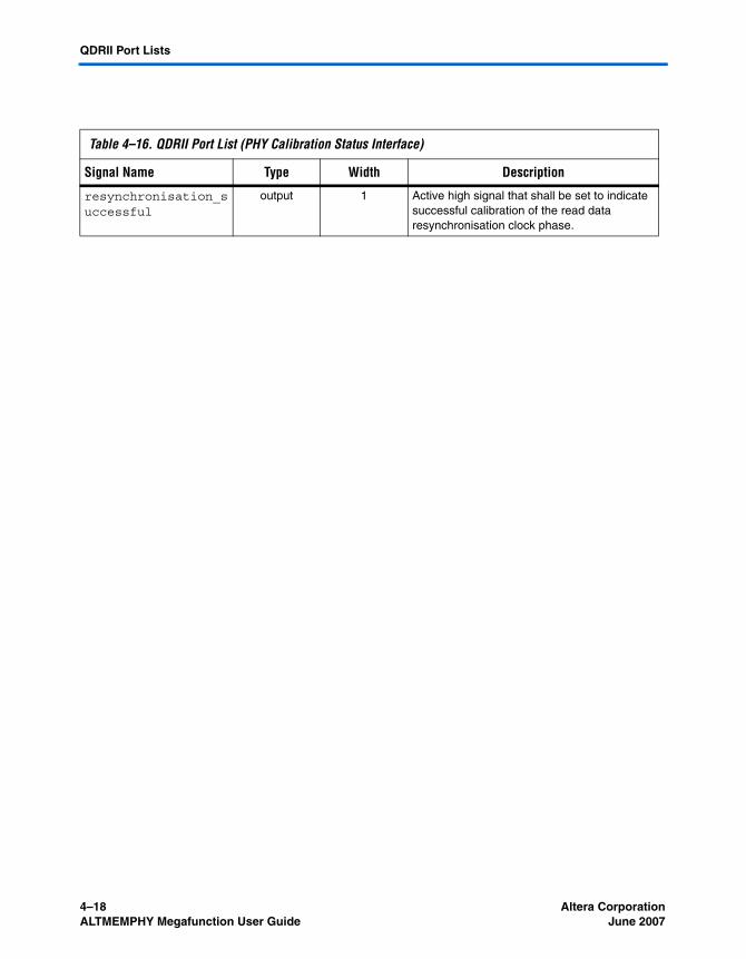
4–18 Altera CorporationALTMEMPHY Megafunction User Guide June 2007
QDRII Port Lists
Table 4–16. QDRII Port List (PHY Calibration Status Interface)
Signal Name Type Width Description
resynchronisation_successful
output 1 Active high signal that shall be set to indicate successful calibration of the read data resynchronisation clock phase.

Altera Corporation A–1June 2007
Appendix A. Latency Numbers
Latency Numbers
There are two types of latencies that exists while designing with memory controllers, they are read and write latencies. Altera® defines the read and write latencies as follows:
■ Read Latency—the amount of time it takes for the read data to appear at the user/local interface after you initiate the read request.
■ Write Latency—the amount of time it takes for the write data to appear at the memory interface after you initiate the write request.
The basic assumptions made while calculating the latencies are:
■ Reading and writing to the rows that are already open■ Local Ready signal is asserted high (no wait states)■ Latency is defined using the user (local) side frequency and absolute
time (ns)
1 For the half-rate controller, the user (local) side frequency is half of the memory interface frequency. For the full-rate controller, the user (local) side frequency is equal to the memory interface frequency.
Altera defines the read and write latencies both in terms of the local interface clock frequency and the absolute time. This applies to the Stratix® II, Stratix III, and Cyclone® III device familes and the following memory controllers:
■ Legacy DDR/DDR2 controller■ High Performance half-rate controller■ High Performance full-rate controller
Tables A–1 and A–2 list the latency for the legacy DDR2 full-rate controller for the Stratix II and Cyclone II device families, respectively.
Table A–1. Latency for Legacy DDR2 Full-Rate Controller (for Stratix II) Note (1) (Part 1 of 2)
Latency Type Latency in Cycles Latency in Time (ns)
Read 13 49
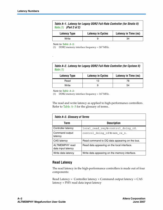
A–2 Altera CorporationALTMEMPHY Megafunction User Guide June 2007
Latency Numbers
.
The read and write latency as applied to high-performance controllers. Refer to Table A–3 for the glossary of terms..
Read Latency
The read latency in the high-performance controllers is made out of four components:
Read Latency = Controller latency + Command output latency + CAS latency + PHY read data input latency
Write 9 34
Note to Table A–1:(1) DDR2 memory interface frequency = 267 MHz.
Table A–2. Latency for Legacy DDR2 Full-Rate Controller (for Cyclone II) Note (1)
Latency Type Latency in Cycles Latency in Time (ns)
Read 13 78
Write 9 54
Note to Table A–2:(1) DDR2 memory interface frequency = 167 MHz.
Table A–3. Glossary of Terms
Term Description
Controller latency local_read_req to control_doing_rd.
Command output latency
control_doing_rd to mem_cs_n.
CAS latency Read command to DQ data appearing on the bus.
ALTMEMPHY read data input latency
Read data appearing on the local interface.
Write data latency Write data appearing on the memory interface.
Table A–1. Latency for Legacy DDR2 Full-Rate Controller (for Stratix II) Note (1) (Part 2 of 2)
Latency Type Latency in Cycles Latency in Time (ns)

Altera Corporation A–3June 2007 ALTMEMPHY Megafunction User Guide
Write Latency
The write latency in the high-performance controllers is made out of three components:
Write Latency = Controller Latency + Write Data latency
1 The latencies due to the above components are listed (in the same order) in Tables A–4 through A–8.
Table A–4. Latency for DDR2 Half-Rate High-Performance Controller (for Stratix II) Note (1)
Latency Type Latency in Cycles Latency in Time (ns)
Read 6 + 4 + 1.5 + 8.5 = 20 60
Write 8 + 3 = 11 33
Note to Table A–4:(1) DDR2 memory interface frequency = 333 MHz.
Table A–5. Latency for DDR2 Full-Rate High-Performance Controller (for Stratix II) Note (1)
Latency Type Latency in Cycles Latency in Time (ns)
Read 6 + 4 + 1.5 + 8.5 = 20 75
Write 8 + 2 = 10 33
Note to Table A–5:(1) DDR2 memory interface frequency = 267 MHz.
Table A–6. Latency for DDR2 Half-Rate High-Performance Controller (for Stratix III) Note (1)
Latency Type Latency in Cycles Latency in Time (ns)
Read 6 + 4 + 1.5 + 8.5 = 20 60
Write 8 + 3 = 11 33
Note to Table A–6:(1) DDR2 memory interface frequency = 333 MHz.

A–4 Altera CorporationALTMEMPHY Megafunction User Guide June 2007
Latency Numbers
Table A–7. Latency for DDR2 Half-Rate High-Performance Controller (for Cyclone III) Note (1)
Latency Type Latency in Cycles Latency in Time (ns)
Read 6 + 4 + 1.5 + 5.5 = 17 85
Write 8 + 3 = 11 55
Note to Table A–7:(1) DDR2 memory interface frequency = 200 MHz.
Table A–8. Latency for DDR2 Full-Rate High-Performance Controller (for Cyclone III) Note (1)
Latency Type Latency in Cycles Latency in Time (ns)
Read 5 + 3 + 3 + 8 = 19 114
Write 8 + 2 = 10 60
Note to Table A–8:(1) DDR2 memory interface frequency = 167 MHz.