altiumlive 2017: introduction to pcb design with altium ... 2/introduction... · altium designer 18...
TRANSCRIPT
AltiumLive 2017:
Introduction to PCB Design with
Altium Designer 18
Chris JenningsLead Global Training
1
EuJin OoiInstructor
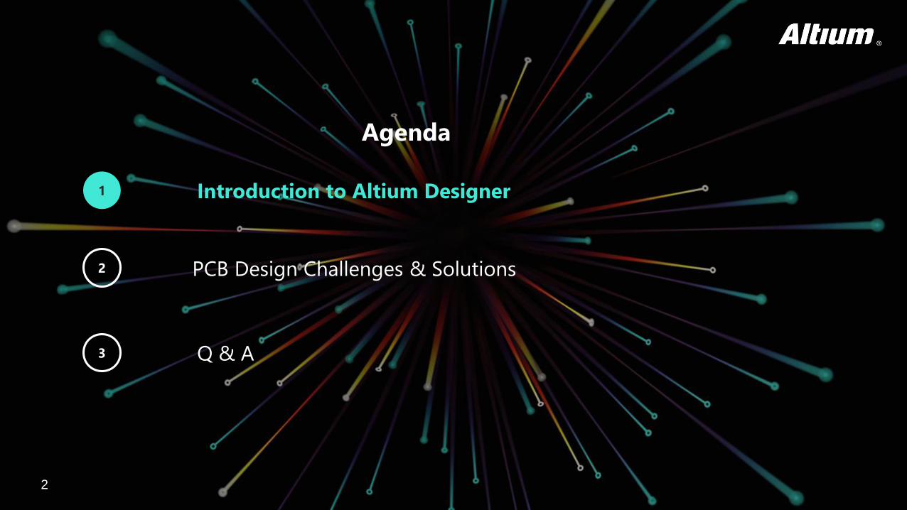
PCB Design Challenges & Solutions
1 Introduction to Altium Designer
Q & A
2
3
Agenda
2
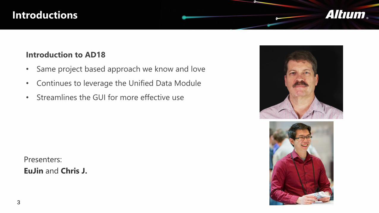
Presenters:
EuJin and Chris J.
Introduction to AD18
• Same project based approach we know and love
• Continues to leverage the Unified Data Module
• Streamlines the GUI for more effective use
Introductions
3
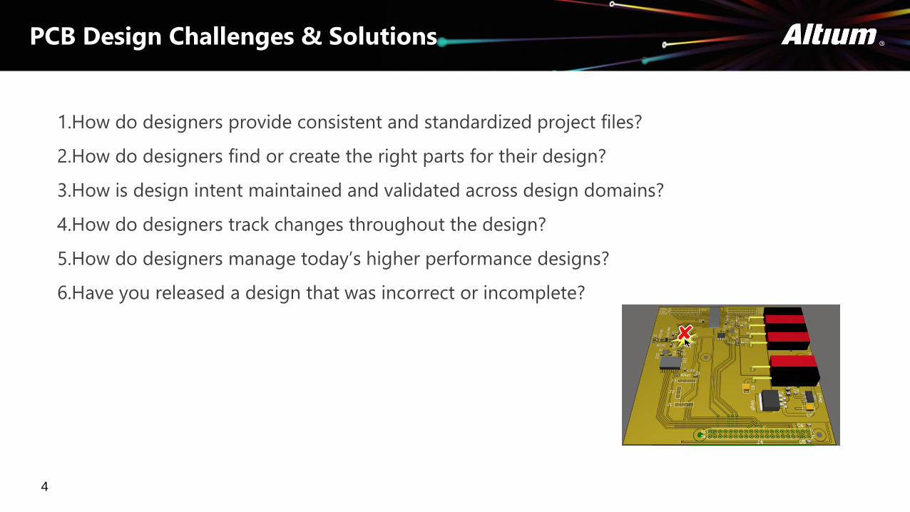
1.How do designers provide consistent and standardized project files?
2.How do designers find or create the right parts for their design?
3.How is design intent maintained and validated across design domains?
4.How do designers track changes throughout the design?
5.How do designers manage today’s higher performance designs?
6.Have you released a design that was incorrect or incomplete?
PCB Design Challenges & Solutions
4
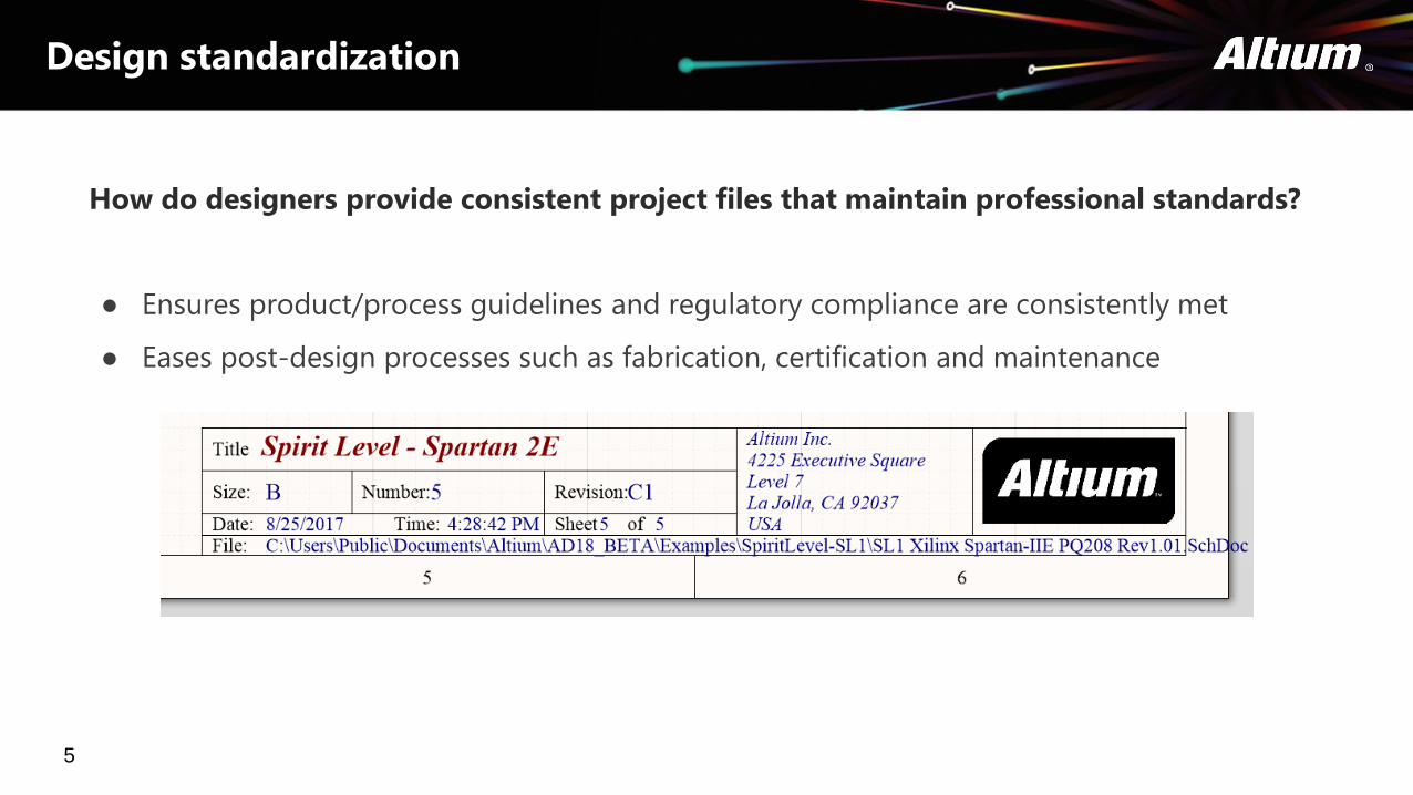
How do designers provide consistent project files that maintain professional standards?
● Ensures product/process guidelines and regulatory compliance are consistently met
● Eases post-design processes such as fabrication, certification and maintenance
Design standardization
5
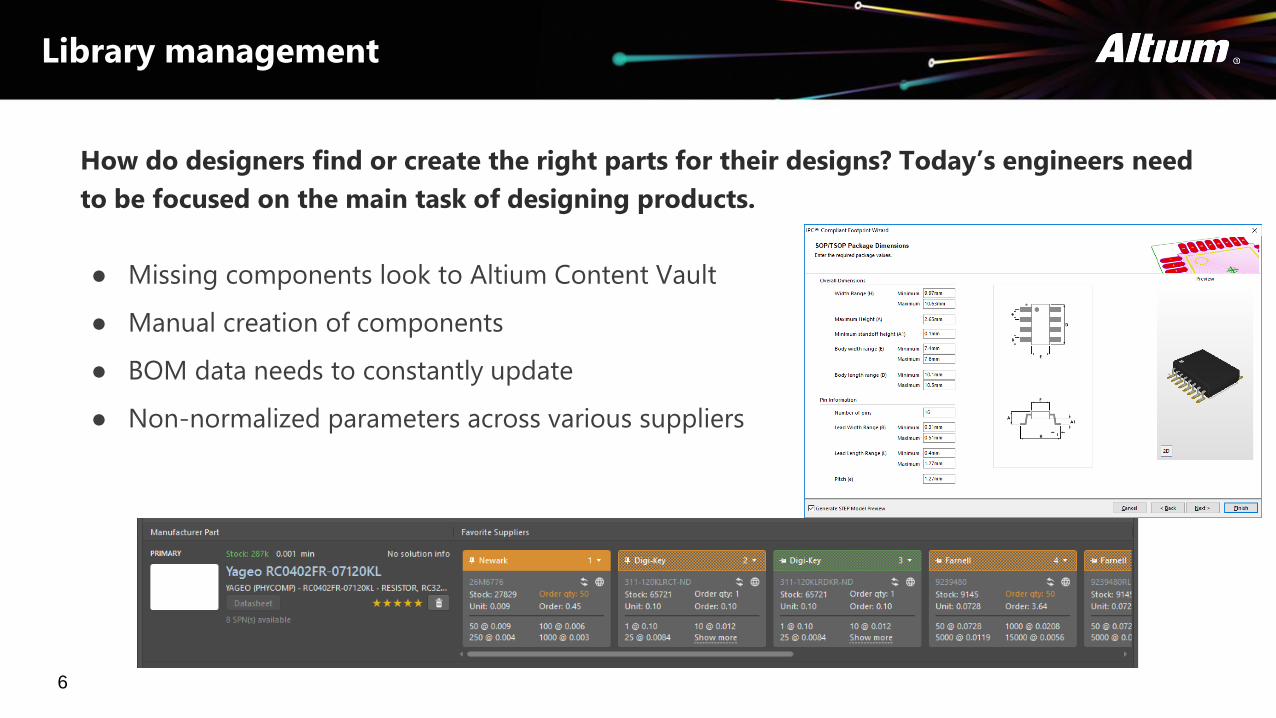
How do designers find or create the right parts for their designs? Today’s engineers need
to be focused on the main task of designing products.
● Missing components look to Altium Content Vault
● Manual creation of components
● BOM data needs to constantly update
● Non-normalized parameters across various suppliers
Library management
6
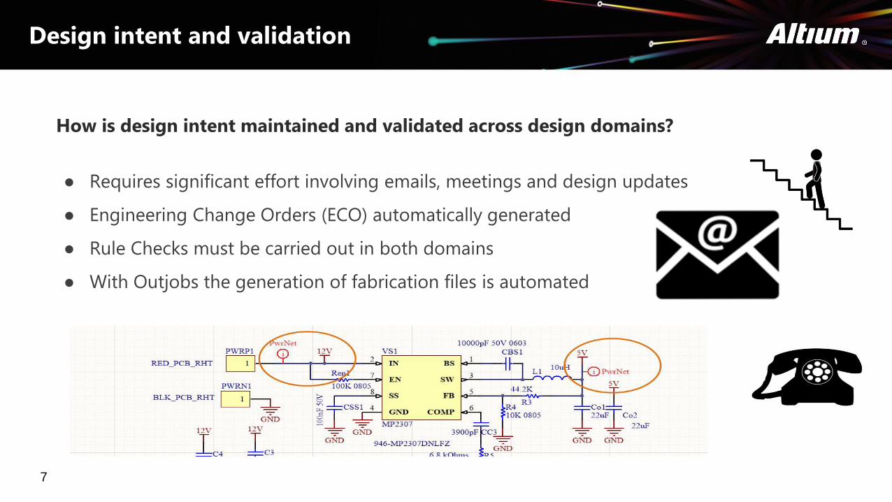
How is design intent maintained and validated across design domains?
● Requires significant effort involving emails, meetings and design updates
● Engineering Change Orders (ECO) automatically generated
● Rule Checks must be carried out in both domains
● With Outjobs the generation of fabrication files is automated
Design intent and validation
7

The tighter constraints of today’s complex designs mean that previously advanced design
techniques have now become mainstream. How does the PCB designer effectively meet
these design challenges?
● Differential pair
● Length tuning
● High speed design rules
● Blind/buried vias
Advanced PCB design techniques
8
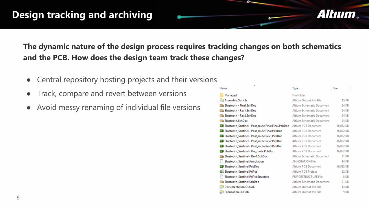
The dynamic nature of the design process requires tracking changes on both schematics
and the PCB. How does the design team track these changes?
● Central repository hosting projects and their versions
● Track, compare and revert between versions
● Avoid messy renaming of individual file versions
Design tracking and archiving
9
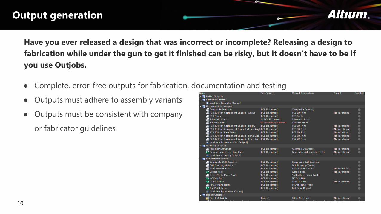
Have you ever released a design that was incorrect or incomplete? Releasing a design to
fabrication while under the gun to get it finished can be risky, but it doesn’t have to be if
you use Outjobs.
● Complete, error-free outputs for fabrication, documentation and testing
● Outputs must adhere to assembly variants
● Outputs must be consistent with company
or fabricator guidelines
Output generation
10
Thank you for your attention.
Questions?
11