alternative materials for next-generation transistors
TRANSCRIPT

Alternative Materials for Next-Generation Transistors:
High-k/Ge-based MOSFET
by
CHIEN-LAN HSUEH
A dissertation submitted to the
Graduate School-New Brunswick
Rutgers, The State University of New Jersey
in partial fulfillment of the requirements
for the degree of
Doctor of Philosophy
Graduate Program in Physics and Astronomy
written under the direction of
Professor Eric Garfunkel
and approved by
New Brunswick, New Jersey
January, 2008
ii
ABSTRACT OF THE DISSERTATION
Alternative Materials for Next-Generation Transistors:
High-k/Ge-based MOSFET
By CHIEN-LAN HSUEH
Dissertation Director:
Professor Eric Garfunkel
Electronic devices that make up 99% of the computer processor and
memory market are based on silicon (semiconductor) and silicon dioxide
(insulator) technology. Unfortunately the key transistor gate stack structure within
the “traditional” technology has reached an intrinsic physical scaling limit; the
ultrathin gate oxide, already at 1nm thickness, cannot be made thinner without
resulting in an intolerably high leakage current and reduced drive current. This
limitation can be avoided by replacing the thin gate dielectric with a thicker film of
an alternative material with a permittivity higher than that of SiO2, an
accomplishing that has been realized in production just as this thesis goes to
press. To further increase device performance, replacing the Si semiconductor
with germanium as an alternative channel material is an attractive option for its
high mobility and narrow band gap. However, the lack of a stable insulating oxide
with high quality electrical properties prevents the fabrication of competitive Ge-
based metal oxide semiconductor field effect transistors (MOSFETs).

iii
This dissertation reports the study of potential future-generation transistors
with high-k dielectrics (HfO2 and Al2O3) on Ge substrates. A brief review of
current research and development is first given followed by an introduction of the
thin film characterization techniques used in this work. Various cleaning
treatments as well as surface passivation methods using wet chemistry have
been investigated on Ge substrates. Next, thin high-k dielectric films of HfO2 and
Al2O3 have been deposited on Ge using atomic layer deposition (ALD). ALD
permits films to be grown with monolayer control and excellent film conformality.
Physical, chemical and electrical characterization has been performed on
the multilayer film structures. Optimization of the film growth has been
developed and we have demonstrated high quality with Au/HfO2/Ge nMOS
devices. Capacitance-voltage electrical measurements show that sulfur
passivation methods on Ge greatly decrease the interface state density and
improve the device electrical properties. The same improvements have also been
observed on the similarly processed Ge-based MOS capacitors with Al2O3
dielectric layers.

iv
In memory of my grand mother
Feng-Lan Hsueh
(1937 - 2007)
“When being normal becomes a luxury,
the world is so distorted that I can barely breath.
Only heavenly love can provide the true guidelines,
that help me no longer hide and cry.”

v
Acknowledgement
I could not have had any better thesis adviser than Prof. Eric Garfunkel.
Without his generousness and encouragement, this dissertation would not have
been possible. He has not only guided me with his knowledge and wisdom, but
also shown me what a true scholar should be.
There is no way for me to come this far without help from people I met
these years. Some gave me essential assistance in my graduate study as well as
my daily life while some shared with me their valuable wisdom and life
experience. I can never express my appreciation enough to all of them. A better
way I have figured to return these favors is to pay them forward to people I will
meet in the journey of my life while keeping in mind that I am what I am, and I
can do what I can do today because of these nice people.
I also owe a lot to my family for their long-lasting patient and support,
especially my wife and my lovely little girls who have always enriched my life with
their endless trust and love.
Chien-Lan Hsueh
Dec 26, 2007
vi
Abbreviation
AES Auger Electron Spectroscopy
AFM Atomic Force Microscopy
ALD Atomic Layer Deposition
ALE Atomic Layer Epitaxy
ARPES Angular Resolved Photoelectron Spectroscopy
BE Binding Energy
CMOS Complementary Metal Oxide Semiconductor
CNL Charge Neutrality Level
CV Capacitance Voltage
CVD Chemical Vapor Deposition
DAQ Data Acquisition
DIW De-ionized Water
DRAM Dynamic Random Access Memory
EELS Electron Energy Lose Spectroscopy
EOT Equivalent Oxide Thickness
ESCA Electron Spectroscopy for Chemical Analysis
FCC Face Centered Cubic
FT-IR Fourier Transform Infrared Spectroscopy
FWHM Full Width at Half Maximum
ITRS International Technology Roadmap for Semiconductors
KE Kinetic Energy
LCD Liquid Crystal Display

vii
LED Light Emitting Diode
LEIS Low Energy Ion scattering
MEIS Medium Energy Ion Scattering
ML Monolayer
MOS Metal Oxide Semiconductor
MOSFET Metal Oxide Semiconductor Field Effect Transistors
NRA Nuclear Reaction Analysis
OLED Organic Light Emitting Device
PC Personal Computer
PDA Post Deposition Annealing
PVD Physical Vapor Deposition
RBS Rutherford Backscattering Spectroscopy
RMS Root Mean Square
RTA Rapid Thermal Annealing
TFEL Thin Film Electroluminescence
TMA Trimethylaluminium
UHV Ultra High Vacuum
USB Universal Serial Bus
UV Ultraviolet
VLSI Very Large Scaled Integrated Circuit
XPS X-ray Photoelectron Spectroscopy

viii
Table of Contents
Title Page .............................................................................................................. i
Abstract .................................................................................................................ii
Acknowledgement ................................................................................................ v
Abbreviation..........................................................................................................vi
Table of Contents ............................................................................................... viii
List of Tables ...................................................................................................... xiii
List of Figures ..................................................................................................... xiv
Chapter 1 Introduction .......................................................................................... 1
Section 1.1 Scaling in CMOS Technology ........................................................ 1
1.1.1 Moore’s Law...................................................................................... 1
1.1.2 Origins of MOSFET Scaling .............................................................. 2
Section 1.2 The Need for Alternative Gate Dielectrics...................................... 5
1.2.1 Reduction of Leakage Current with High-k Dielectric ........................ 5
1.2.2 Effective Oxide Thickness ................................................................. 7
1.2.3 Guidelines for Choosing High-k Dielectric ......................................... 7
Section 1.3 Germanium-based MOSFET ......................................................... 9
1.3.1 Germanium ....................................................................................... 9

ix
Section 1.4 Passivation of Germanium ........................................................... 12
1.4.1 Passivation with Hydrogen .............................................................. 13
1.4.2 Passivation with Nitrogen ................................................................ 14
1.4.3 Passivation with Chlorine ................................................................ 14
1.4.4 Passivation with Sulfur .................................................................... 15
Section 1.5 Objectives of This Study .............................................................. 15
Section 1.6 Structure of the Dissertation ........................................................ 16
Section 1.7 Reference .................................................................................... 17
Chapter 2 Thin Film Characterization Techniques .............................................. 21
Section 2.1 X-ray Photoelectron Spectroscopy .............................................. 21
2.1.1 Principle of XPS .............................................................................. 22
2.1.2 Atomic Sensitivity Factor ................................................................. 25
2.1.3 Depth Profiling Using XPS .............................................................. 26
Section 2.2 Rutherford Backscattering Spectroscopy..................................... 30
2.2.1 Kinematics of RBS .......................................................................... 31
2.2.2 Scattering Cross Section and Areal Density of Target Atoms ......... 34
2.2.3 Depth Profiling Using RBS .............................................................. 36
2.2.4 Channeling ...................................................................................... 39
2.2.5 SIMNRA .......................................................................................... 40

x
Section 2.3 AFM ............................................................................................. 41
2.3.1 Principle of AFM.............................................................................. 41
2.3.2 Quantification of Surface Roughness .............................................. 42
Section 2.4 FT-IR ........................................................................................... 43
2.4.1 Absorption Spectroscopy ................................................................ 43
2.4.2 Infrared Spectroscopy ..................................................................... 45
2.4.3 FT-IR ............................................................................................... 46
Section 2.5 Reference .................................................................................... 49
Chapter 3 Preparation of Germanium Substrates ............................................... 51
Section 3.1 Cleaning of Germanium Substrates ............................................. 51
3.1.1 Native Oxides.................................................................................. 52
3.1.2 Removal of Native Oxide and Carbon ............................................. 55
3.1.3 Protective Chemical Oxides ............................................................ 60
Section 3.2 Passivation on Germanium Substrates........................................ 65
3.2.1 Passivation with Hydrogen .............................................................. 66
3.2.2 Passivation with Sulfur .................................................................... 69
Section 3.3 Reference .................................................................................... 76
Chapter 4 Atomic Layer Deposition of High-k Dielectrics .................................... 78
Section 4.1 Atomic Layer Deposition .............................................................. 78
xi
4.1.1 Advantages of ALD Processes ....................................................... 79
Section 4.2 Metal Precursors ......................................................................... 84
4.2.1 Precursors for Al2O3 ........................................................................ 85
4.2.2 Precursors for HfO2 ......................................................................... 87
4.2.3 Precursors for ZrO2 ......................................................................... 91
Section 4.3 Oxygen Sources .......................................................................... 93
Section 4.4 ALD System ................................................................................. 95
Section 4.5 Experimental Results of ALD Film Growths ................................. 98
4.5.1 ALD of Al2O3 ................................................................................... 98
4.5.2 ALD of HfO2 .................................................................................. 101
Section 4.6 Reference .................................................................................. 104
Chapter 5 High-k/Ge MOS Capacitors .............................................................. 111
Section 5.1 C-V Measurements .................................................................... 111
5.1.1 Energy Band Diagrams of MOS Stacks and Flat-Band Voltage ... 111
5.1.2 C-V Curves of MOS Capacitors and Threshold Voltage ............... 118
Section 5.2 Effects of Trapped Charges on C-V Curves .............................. 124
5.2.1 Shifts of Flat-Band Voltage and Hysteresis of C-V Curves ........... 124
5.2.2 Determination of Interface Traps................................................... 126
Section 5.3 Experimental Results ................................................................. 127

xii
5.3.1 HfO2/Ge ........................................................................................ 128
5.3.2 Al2O3/Ge ....................................................................................... 133
Section 5.4 Reference .................................................................................. 135
Chapter 6 Conclusion ....................................................................................... 136
Curriculum Vista ............................................................................................... 139

xiii
List of Tables
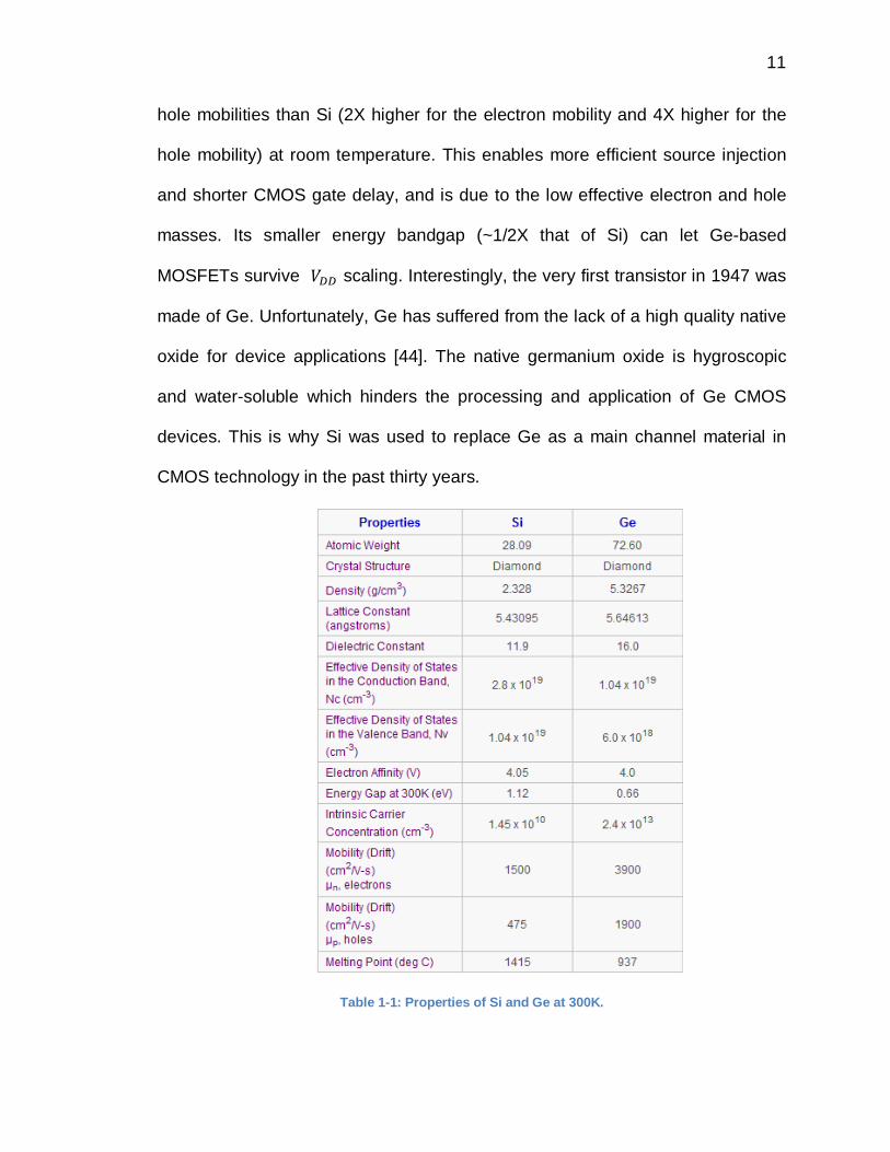
Table 1-1: Properties of Si and Ge at 300K. ....................................................... 11
Table 2-1: Values of XPS atomic sensitivity factors used in this work [7]. .......... 26
Table 3-1: Comparison of XPS atomic concentration (%) of S-passivated
samples with different cleaning. ........................................................ 75
Table 4-1: List of common Al precursors used in ALD. ....................................... 86
Table 4-2: List of common Hf precursors used in ALD. ...................................... 90
Table 4-3: List of common Zr precursors used in ALD. ...................................... 92
Table 5-1: Comparison of the C-V measurements on Au/HfO2/p-Ge(100)
capacitors. ....................................................................................... 132

xiv
List of Figures
Figure 1-1: Number of transistors within a die over time [10]................................ 2
Figure 1-2: The structure of n-channel MOSFET. ................................................. 3
Figure 1-3: Equivalent oxide thickness scaling in International Technology
Roadmap for Semiconductors [1]. ..................................................... 5
Figure 1-4: Suppression of the direct tunnel leakage current by introducing a
high-k gate oxide. .............................................................................. 6
Figure 1-5: Bandgap as a function of dielectric constant for several alternative
high-k dielectrics [43]. ........................................................................ 9
Figure 1-6: Bandgap and lattice constants of the most relevant semiconductor
materials related to germanium. ...................................................... 10
Figure 2-1: Schematic drawing of XPS system................................................... 22
Figure 2-2: Energy-level diagrams showing the electron transitions in XPS. ...... 23
Figure 2-3: Comparison of XPS (a) and RBS (b) depth profiling on a Ge/SiO2/Si
sample annealed in O2 [9]. ............................................................... 27
Figure 2-4: Mean free path of photoelectrons in solid [10]. ................................. 28
Figure 2-5: Geometry of angle resolved XPS setup. .......................................... 29
Figure 2-6: Rutherford Back Scattering Spectroscopy (RBS). ............................ 31
Figure 2-7: The position of RBS peaks reflects the mass difference of targets. . 32
Figure 2-8: Kinematic factor for He+ ions backscattering from different masses at
different scattering angles. ............................................................... 33

xv
Figure 2-9: Kinematic factor for He+ ions backscattering from different targets at
different scattering angles. ............................................................... 33
Figure 2-10: The position of RBS peaks reflects the depth distribution of targets.
......................................................................................................... 37
Figure 2-11: Channeling is the guided motion of ions in the open channels of a
crystal target. ................................................................................... 39
Figure 2-12: Random and channeled spectrum of 270 keV He+ incident on 25Å
SiO2/Si along <111> [21]. ................................................................ 40
Figure 2-13: A schematic drawing of an AFM system. ....................................... 42
Figure 2-14: Some normal modes of –CH2 molecular vibrations. The + and –
symbols indicate a movement out of and into the plane of the paper
respectively. ..................................................................................... 46
Figure 2-15: Schematic drawing of components of FT-IR and the Michelson
interferometer. ................................................................................. 47
Figure 3-1: Ge 3d XPS spectrum from as-received Ge(100) wafers. ................. 53
Figure 3-2: Ge 3d XPS spectra of an as-received Ge(100) sample at different
take-off angles. ................................................................................ 54
Figure 3-3: Calculation of the thickness of the oxide overlayer on Ge(100). ...... 55
Figure 3-4: Ge 3d XPS spectrum from a Ge(100) wafer after DIW rinsing. ........ 56
Figure 3-5: Ge 3d XPS spectrum from a Ge(100) wafer after the 10% HF etching.
......................................................................................................... 57
Figure 3-6: C 1s XPS spectra from as-received, DIW-rinsed and HF-etched
Ge(100) samples. ............................................................................ 58

xvi
Figure 3-7: Ge 3d XPS spectra as a function of annealing temperature [22]. ..... 59
Figure 3-8: C 1s (left) and O 1s (right) XPS spectra from Ge(100) after UV/ozone
exposure and annealing [3].............................................................. 61
Figure 3-9: Ge 3d XPS spectrum from a Ge(100) sample with a chemical oxide
formed by concentrated H2O2. ......................................................... 62
Figure 3-10: Ge 3d XPS spectrum from a Ge(100) sample with chemical oxide
formed by H2SO4/H2O2. ................................................................... 63
Figure 3-11: Comparison of C 1s XPS peaks with different cleaning methods. .. 63
Figure 3-12: Intensity changes of C 1s XPS peaks before and after the removal
of chemical oxide. ............................................................................ 64
Figure 3-13: Etching and chemical oxidization on as-received Ge wafers. ......... 65
Figure 3-14: FT-IR spectra of a H-terminated Ge(100) sample (blue) vs.
H2SO4/H2O2-treated Ge sample followed by a DIW rise (red) using
as-received Ge samples as a reference. ......................................... 66
Figure 3-15: FT-IR spectra of HF-etched Ge(100) after a different wet chemical
cleaning is applied. .......................................................................... 68
Figure 3-16: FT-IR spectra to show the stability of H-terminated Ge(100) in air
and in N2. ........................................................................................ 69
Figure 3-17: Molecular structure of thioacetamide and thiourea. ........................ 70
Figure 3-18: S 2p XPS spectra from Ge(100) treated in (NH4)2S, thioacetamide
and thiourea solution. ...................................................................... 70
Figure 3-19: Ge 3d XPS spectrum from a (NH4)2S-treated Ge(100) sample. ..... 71

xvii
Figure 3-20: Ge 2p XPS spectrum from a S-passivated H2SO4/H2O2-treated
Ge(100) sample. The inset shows the comparison of the same
sample (red line) with an as-received sample (blue line). ................ 73
Figure 3-21: S 2p and C 1s XPS spectra from S-passivated Ge samples with
different cleaning pretreatments. ..................................................... 73
Figure 4-1: Schematic drawing of one ALD cycle (adapted from [12]). ............... 80
Figure 4-2: Different types of growth rate vs. precursor pulse time at a constant
temperature [12]. ............................................................................. 81
Figure 4-3: Factors that prevent full surface coverage of chemisorption: (a) steric
hindrance of the ligands, and (b) number of reactive surface sites
[10]. .................................................................................................. 82
Figure 4-4: Factors limiting the self-limiting growth at various temperatures [12].
......................................................................................................... 83
Figure 4-5: Molecular structure of metal halide................................................... 85
Figure 4-6: Molecular structures of metal alkyls. ................................................ 87
Figure 4-7: Molecular structures of metal alkyamides. ....................................... 89
Figure 4-8: The integrated XPS system with ALD and metallization chambers. . 95
Figure 4-9: The schematic drawing of the ALD system. ..................................... 97
Figure 4-10: RBS random scattering spectrum of Al2O3 of the same thickness on
Si (left) and Ge (right). ..................................................................... 99
Figure 4-11: RBS spectra of Al2O3 on ITO (left) and Kapton (right). ................. 100
Figure 4-12: Film thickness of Al2O3 vs. number of ALD cycles. ...................... 101
Figure 4-13: Random scattering RBS spectrum of HfO2/GaAs. ........................ 102

xviii
Figure 4-14: Film thickness of HfO2 vs. number of ALD cycles. ....................... 102
Figure 4-15: Random scattering RBS spectrum of HfO2/Ge (left) and HfO2/Si
(right). ............................................................................................ 103
Figure 4-16: Film thickness of HfO2 on Ge (left) and on Si (right) vs. number of
ALD cycles. .................................................................................... 103
Figure 5-1: Energy band diagram of an ideal MOS capacitor [1]. ..................... 112
Figure 5-2: Space-charge density as a function of the surface potential for p-type
Ge with NA=2.5x1022 cm-3 at room temperature. ............................ 114
Figure 5-3: Band diagrams for an ideal p-substrate MOS structure in different
surface-charge conditions (adapted from [1-3]). ............................ 115
Figure 5-4: Band diagrams of MOS (a) at separation, (b) at equilibrium and (c) in
flat-band condition [3]. ................................................................... 116
Figure 5-5: (a) Charges represented as a sheet of effective charge [2]; (b)
interface traps [7]. .......................................................................... 118
Figure 5-6: Equivalent circuits including interface-trapped effects (a), at high (b)
and low frequency (c). ................................................................... 119
Figure 5-7: Band diagram and distribution of charge density in inversion [1, 3].
....................................................................................................... 121
Figure 5-8: C-V curve for an ideal p-substrate MOS capacitor at high (HF) and
low (LF) frequency [7]. ................................................................... 122
Figure 5-9: C-V curve with nonzero work function difference (dashed) and
trapped charges (dotted) [7]........................................................... 125
Figure 5-10: Hysteresis of a C-V curve [7]. ....................................................... 126

xix
Figure 5-11: C-V curves at high (solid line) and low (dotted line) frequencies [7].
....................................................................................................... 127
Figure 5-12: Schematic drawing of the C-V measurement setup. .................... 128
Figure 5-13: C-V curves of a Au dot capacitor with 4 nm HfO2 on HF-last p-
Ge(100).......................................................................................... 129
Figure 5-14: C-V curves of a Au dot capacitor with 4 nm HfO2 on HF/DIW/H2O2-
treated S-passivated p-Ge(100). .................................................... 130
Figure 5-15: C-V curves of a Au dot capacitor with 4 nm HfO2 on H2SO4/H2O2
oxidized, HF-etched S-passivated p-Ge(100). ............................... 131
Figure 5-16: C-V curves of a Au dot capacitor with 4 nm HfO2 on H2SO4/H2O2
oxidized, S-passivated p-Ge(100). ................................................. 132
Figure 5-17: C-V curves of Al dot capacitors with 7.7 nm HfO2 on S-passivated n-
Ge(100) [12]................................................................................... 133
Figure 5-18: C-V curves of Au/Al2O3/p-Ge(100) with (right) and without (left) the
sulfur passivation. .......................................................................... 134

1
Chapter 1 Introduction
Section 1.1 Scaling in CMOS Technology
The key to the growth of the microelectronics industry during the last 30
years has been the drive to ever smaller dimensions using the principles of
“device scaling”. The basic idea of scaling is to reduce the dimensions of
electronic devices for computation and memory in order to increase the density
and speed of integrated circuits, and decrease the cost and power consumption
per unit function.
1.1.1 Moore’s Law
The semiconductor industry has been growing and prospering
continuously since the early 1970s. Each month smaller and faster electronic
products appear on the market due to of the rapid growth of semiconductor
technology. In order to satisfy the demand for faster circuits, higher packing
density and lower power dissipation, the dimensions of metal–oxide–
semiconductor field-effect transistor (MOSFET) devices (complementary MOS,
CMOS, in particular) are being scaled down according to the International
Technology Roadmap for Semiconductors (ITRS) [1], a guidebook for the field.
Gordon Moore, one of the founders of Intel predicted that the number of
transistors on a chip would quadruple every 36 months, later updating his
prediction to quadrupling every 24 months [2, 3]. This prediction is known as

2
Moore’s Law. The number of transistors in an integrated circuit was about 2000
at the time he made his observation. By the end of the current decade, one billion
transistors (per die) will be achieved. Figure 1-1 illustrates this for a range of
processor families [4-9].
Figure 1-1: Number of transistors within a die over time [10].
1.1.2 Origins of MOSFET Scaling
Figure 1-2 shows the structure of an n-channel MOSFET. In the dorminant
Si technology, the main dielectric material of the MOS capacitor, SiO2 (recently
SiON), is sandwiched between doped poly-silicon (the gate) and a Si substrate.
While applying a positive bias on the gate, an electric field across the dielectric
layer will draw electrons into the region just below the dielectric, forming a
conductive channel, the n-channel, and switch on the device.

3
Figure 1-2: The structure of n-channel MOSFET.
The drain-source current for a long-channel MOSFET operating in the
saturation region is given by, 12 where is the channel mobility, and are the width and length of the channel
region, respectively, is the gate-source potential, and is the threshold
voltage.
In order to increase the drain-source current , one can optimize the
device by (1) reducing the length of the channel , (2) increasing the channel
mobility of the substrate, and (3) increasing the MOS capacitance :
(1) Shrinking of the transistor gate length reduces the carriers travelling
distance and hence the time between source and drain; thus the drain-source
current increases and the device speed increases. Reducing the gate oxide
thickness along with the channel length also helps to maintain the gates
electrode control over deleterious “short channel” effects [11].

4
(2) Replacing silicon with a higher channel-mobility semiconductor to
increase will be discussed in detail in Section 1.3.
(3) The capacitance of a MOS capacitor, essentially a parallel plate
capacitor, is given as,
where is the relative permittivity of the gate oxide (dielectric constant), is the
permittivity of vacuum, is the capacitor area, and is the gate oxide physical
thickness. Either reducing the thickness of the gate oxide layer or using
dielectric materials with a higher dielectric constant , will helps increase the gate
capacitance . This allows the gate potential to modulate more channel charge
and is especially important as the supply voltage scales down.
Much of the progress in Si microelectronics has been driven by the ability
to continually shrink the lateral ( and ) and vertical dimensions of the
MOSFET to increase performance and decrease die area, a process referred to
as scaling [12]. In order to maintain the same transistor parameters such as
threshold voltage and capacitance, the shortening of the transistor channel
length leads to a corresponding scaling of the gate area and gate oxide
thickness [11].
To be able to follow scaling according to the ITRS, the SiO2 film thickness
used in manufacturing should be below 1nm within the next few years as shown
in Figure 1-3, or a new dielectric must be used (more details in next section).

5
Figure 1-3: Equivalent oxide thickness scaling in I nternational Technology Roadmap for
Semiconductors [1].
Section 1.2 The Need for Alternative Gate Dielectri cs
Scaling of traditional CMOS technology with SiO2 results in a dramatic
increase in leakage current and degrades the device performance. Higher
permittivity (high-k) dielectric materials and metal electrodes are now considered
as the best way to solve the leakage problem while continuing to scale devices.
1.2.1 Reduction of Leakage Current with High-k Diel ectric
Traditional scaling, which has guided, and in some sense driven the
semiconductor industry for the last 30 years, is reaching some fundamental limits
when using standard material building blocks of the CMOS process [1, 13-15].

6
One of the biggest challenges in the traditional process shrinking approach is the
SiO2 gate insulator.
Thermally grown oxide (SiO2) has been used as a gate dielectric since the
introduction of MOSFET devices. Because silicon dioxide has high compatibility
with Si substrate, simple grow-process on Si and excellent insulator properties,
Si has been the leading semiconductor for decades. However, as this thin SiO2
gate oxide of only a few atomic layers is scaled below 1.5 nm, it permits a
dramatic increase in the direct tunnel leakage current through the insulator and
reduces the drive current. Gate leakage current reduces the on-off current ratio
of the device, creating heat which could possibly lead to a break-down of the
device. This causes the fundamental limitation to further scaling.
Figure 1-4: Suppression of the direct tunnel leakag e current by introducing a high-k gate oxide.
The high leakage current and the inadequate reliability of the SiO2 layer
less than ~1.5 nm thick suggests a need for a replacement of SiO2 with a thicker
dielectric material with a higher permittivity . High k dielectrics reduce the
leakage current by providing a thicker film while electrically behaving as a thinner
7
equivalent dielectric as illustrated in Figure 1-4. Therefore high-k materials are
excellent candidates for replacements to the traditional SiO2 gate oxide.
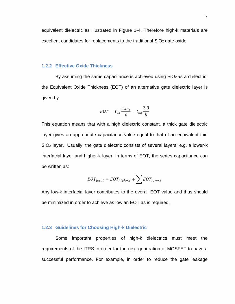
1.2.2 Effective Oxide Thickness
By assuming the same capacitance is achieved using SiO2 as a dielectric,
the Equivalent Oxide Thickness (EOT) of an alternative gate dielectric layer is
given by: 3.9
This equation means that with a high dielectric constant, a thick gate dielectric
layer gives an appropriate capacitance value equal to that of an equivalent thin
SiO2 layer. Usually, the gate dielectric consists of several layers, e.g. a lower-k
interfacial layer and higher-k layer. In terms of EOT, the series capacitance can
be written as:
Any low-k interfacial layer contributes to the overall EOT value and thus should
be minimized in order to achieve as low an EOT as is required.
1.2.3 Guidelines for Choosing High-k Dielectric
Some important properties of high-k dielectrics must meet the
requirements of the ITRS in order for the next generation of MOSFET to have a
successful performance. For example, in order to reduce the gate leakage

8
current, a dielectric constant value of 8-30, a barrier height greater than 1.0 eV
between the substrate and the dielectric [16, 17] and a sufficient bandgap (>5
eV) [17] are required. If the dielectric constant is too high, a large electric field will
exist along the channel edges. If the barrier height is too low, it will increase the
tunneling across the gate. A general trend from Clausius-Mosotti relation is that,
as the dielectric constant increases, the bandgap decreases. This leads to lower
barrier heights and hence greater thermal emission and tunneling.
From a process point of view, candidates of alternative gate dielectrics
must meet a set of criteria such as thermodynamic stability, interface quality, and
film morphology [18]. Many dielectric materials have been investigated, but very
few appear promising with respect to all the guidelines listed above. These
include the group IIIB metal oxide Al2O3 [19-24], the group IVA metal oxides HfO2
[25-29], ZrO2 [30-34] and the group VA oxide Ta2O5 [35-37]. Oxides of binary
alloys, such as ZrAlxOy [38, 39] have also been studied because of the attempt to
combine the desirable qualities of the two metal oxides while eliminating the
undesirable properties of each individual material. Metal silicates such as Zr and
Hf-silicates are also considered as promising materials because they exhibit high
thermal stability [40-42].
Furthermore, an alternative gate dielectric should have a low oxygen
diffusivity, a low density of defects and a high thermal stability with the substrate
so that interfacial reactions with the adjacent layers are minimized. The
requirements mentioned above limit the gate dielectric candidates to only a few
(Figure 1-5), among which the oxides of Al, Hf and Zr are the most promising.

9
Figure 1-5: Bandgap as a function of dielectric con stant for several alternative high-k dielectrics [4 3].
Section 1.3 Germanium-based MOSFET
Using semiconductors with high channel mobility can also improve the
performance of MOSFETs by enabling faster speed and lower power dissipation.
Germanium has drawn a lot of attention to replace Si for the next generation of
CMOS technology, and is already used in other high performance devices.
1.3.1 Germanium
Germanium, like silicon, is a group IV element which has a diamond lattice
composed of two interpenetrating face centered cubic (FCC) lattices, each

10
displaced 1/4 of a lattice constant in each direction from one another. Each site is
tetrahedral coordinated with four other sites in the other sublattice. Among the
elements of group IV, only Ge and Si are widely used as semiconductors.
The main uses for Ge are in transistors and as dopant materials in optical
fibers. As substrates, Ge is also extensively used in epitaxial growth of III-V
compounds. The lattice constant of non-polar Ge is 5.6461 Å at room
temperature, having less than 1% difference than the polar GaAs lattice constant
of 5.6537 Å. This suitable value of Ge lattice constant enables several
semiconductor compounds to be grown on it without a significant strain field.
Figure 1-6: Bandgap and lattice constants of the mo st relevant semiconductor materials related to
germanium.
Ge has been considered as a replacement channel material of Si for
future high-speed CMOS technology because bulk Ge has higher electron and
11
hole mobilities than Si (2X higher for the electron mobility and 4X higher for the
hole mobility) at room temperature. This enables more efficient source injection
and shorter CMOS gate delay, and is due to the low effective electron and hole
masses. Its smaller energy bandgap (~1/2X that of Si) can let Ge-based
MOSFETs survive scaling. Interestingly, the very first transistor in 1947 was
made of Ge. Unfortunately, Ge has suffered from the lack of a high quality native
oxide for device applications [44]. The native germanium oxide is hygroscopic
and water-soluble which hinders the processing and application of Ge CMOS
devices. This is why Si was used to replace Ge as a main channel material in
CMOS technology in the past thirty years.
Table 1-1: Properties of Si and Ge at 300K.

12
In potential future Ge-based CMOS and photo detectors, a high quality
Ge-dielectric interface is essential to device performance. High-k gate dielectric
MOS transistors based on Ge have been investigated in the hope that deposited
high-k gate dielectrics may exhibit better electrical characteristics than the poor
quality germanium oxide gate dielectric layer. High-k gate insulators made of
HfO2 [45-47], Al2O3 [47] and ZrO2 [48] as well as germanium oxy-nitride [49] have
recently been studied for Ge-based MOSFET devices.
Section 1.4 Passivation of Germanium
Ge, like Si, substrates are very reactive toward oxygen and other species,
In part because of the dangling bonds on the surface. Surface passivation, the
termination of these bonds with elements like H, N and S, helps stabilize the
surface. Passivation of Ge substrates is necessary to minimize contamination of
the surface. For example, without surface passivation, Ge substrates can be
inert-gas ion-sputtered in order to obtain a clean Ge surface, although this
degrades the surface severely by inducing damage [50, 51].
A related, in some sense more general, reason to passivate Ge surfaces
is to improve the dielectric/Ge interface which greatly affects the performance of
the device. When high-k materials are used as the gate dielectric on Ge, serious
problems arise during processing. The most challenging one is the formation of
an interfacial GeOx layer between the high-k gate dielectric and the Ge substrate
during the deposition of high-k dielectrics or post annealing processes [52]. Since

13
a high temperature process is required to activate dopants in the source and the
drain, it can lead to unwanted reactions: (1) between the dielectric and Ge, (2) in
the dielectric, (3) between the dielectric and the metal gate, and/or (4) metal
diffusion through the gate dielectric and into the channel. This makes it very
difficult to have the ultra thin EOTs needed in future devices. High temperatures
also change the film morphology of the dielectric into crystalline or polycrystalline
materials. The leakage current increases and the flatband and threshold voltages
can shift due to several reasons, including the large grain boundaries associated
with a polycrystalline film allowing carriers and dopants to move more easily
through the material.
To summarize, an effective passivation treatment should be chemically
stable, protect the substrate from unwanted oxidation and contamination, and
help minimize interface or surface-induced carrier recombination. In order to
achieve these, clean Ge surfaces are usually passivated by saturating the
surfaces with H, N, Cl, S, or other species as discussed below.
1.4.1 Passivation with Hydrogen
One possible way to passivate Ge is to saturate dangling bonds on the
surface with hydrogen. Because of the success of hydrogen passivation on Si
substrates in the development of the semiconductor industry, hydrogen
passivation on Ge substrates has been studied [53, 54]. Clean oxygen-free H-
terminated Ge surfaces can be obtained with wet chemical treatments. However,

14
like H-terminated Si, the stability of H-terminated Ge is not good. Bodlaki has
reported that the H-terminated Ge(111) surface is very unstable under ambient
conditions [55]. Rapid absorption of hydrocarbons has also been observed on H-
terminated Ge(100) [56].
1.4.2 Passivation with Nitrogen
Nitrogen addition (nitridation) is also used to improve the reliability of Ge-
based MOSFETs through the formation of strong Ge-N bonds [57-60]. The
nitrogen incorporation, with Ge to form a Ge oxynitride or Ge nitride layer,
provides higher thermal stability and a higher dielectric constant than that of
GeOx. These nitride-based dielectrics can be used not only as a buffer layer for
the growth of high-k gate dielectrics on Ge, but also as a gate insulator for Ge-
based MOSFET [59-65].
1.4.3 Passivation with Chlorine
Cl-terminated Ge surfaces are prepared usually with hydrogen chloride
(HCl) [66, 67]. The etching mechanism is different on Ge(100) and Ge(111)
surfaces. On the Ge(111) surface, only Ge mono-chloride is formed [67]. Both
Ge mono-chlorides and di-chlorides are found on Ge(100) surfaces [66].
However, the Cl-terminated Ge surfaces are not stable in air; their rapid re-
oxidization is thought to be due to incomplete Cl-termination [55].

15
1.4.4 Passivation with Sulfur
Another promising solution is using sulfur to passivate a Ge substrate
before the deposition of high-k gate dielectrics. Similar to nitridation discussed
above, this sulfur passivation layer can also form a buffer layer to prevent the
formation of interfacial GeOx. Experimental [68-71] and theoretical [72, 73]
studies of low pressure adsorption of sulfur on clean Ge(100) have shown that
the sulfur is bridge bonded to the surface Ge atoms. Furthermore, for a sulfur
coverage of 1 ML, all of the Ge dangling bonds are saturated, resulting in the
S/Ge(100)-1x1 surface being ideally terminated [69]. Recently, Ge surface
passivation with sulfur using aqueous ammonia sulfide (NH4)2S has been
demonstrated [74-76]. The S-terminated Ge surface proves to be much more
stable in air than H- and Cl-terminated Ge surfaces [55]. Compared to nitridation,
sulfur passivation resulting high-k/S-Ge/Ge stacks yields a lower fixed charge
and interface state density as well as higher stability [74] and lower Schottky
barrier height [75], as will be discussed in more detail below.
Section 1.5 Objectives of This Study
The purpose of this work is to investigate the effects of wet chemical
cleaning and sulfur passivation on Ge and show the improvements to
performance of high-k dielectric Ge MOSFET, especially the lower interface
trapped charges and interface state density. Device parameters will be extracted
from electrical property measurements of MOSFET devices.

16
Section 1.6 Structure of the Dissertation
This dissertation will correlate the material properties (physical and
chemical) with device electrical characterization.
Chapter 2 is a description of the surface characterization techniques used
in this work.
Chapter 3 investigates the effects of different wet chemical cleaning
methods on Ge and optimizes the process of sulfur passivation.
Chapter 4 describes the mechanism of atomic layer deposition used in this
work for the deposition of high-k dielectrics, as well as the home-made ALD
system that we built.
Chapter 5 provides a detailed introduction to capacitance-voltage
measurements as an electrical characterization technique to investigate the
improvements of high-k/Ge-based MOSFET with different cleaning and
passivation methods on Ge surfaces.
Chapter 6 concludes the thesis and proposes future works.

17
Section 1.7 Reference
1. International Technology Roadmap for Semiconductors. Available from: http://www.itrs.net/home.html.
2. G.E. Moore, Cramming more components onto integrated circuits. 1965: p. 114-117. 3. G.E. Moore. Progress in digital integrated electronics. in IEDM. 1975. Washington D.C.,
USA. 4. L.A. Barroso, The price of performance. ACM Queue, 2005. 3(7): p. 48-53. 5. N. Corporation, NVIDIA GeForce 8800 GPU Architecture Overview. Technical Brief TB-
02787-001_v01, NVIDIA Corporation, 2006. 6. J. Friedrich, B. McCredie, N. James, et al., Design of the POWER6 Microprocessor. In IEEE
International Solid-State Circuits Conference (ISSCC 2007), 2007. 7. M. Golden, S. Arekapudi, G. Dabney, et al., A 2.6GHz Dual-Core 64b x86 Microprocessor
with DDR2 Memory Support. In IEEE International Solid-State Circuits Conference (ISSCC 2006), 2006.
8. R. Ronen, A. Mendelson, K. Lai, et al., Coming challenges in microarchitecture and architecture. Proceedings of the IEEE, 2001. 89(3): p. 325-340.
9. M.Y. N. Sakran, M. Mehalel, J. Doweck, E. Knoll, and A. Kovacs, Implementation of the 65nm dual-core 64b merom processor. In IEEE International Solid-State Circuits Conference (ISSCC 2007), 2007.
10. C. Isci, A. Buyuktosunoglu, and M. Martonosi, Long-term workload phases: Duration predictions and applications to DVFs. Ieee Micro, 2005. 25(5): p. 39-51.
11. S.M. Sze, Physics of Semiconductor Devices. 2nd ed. 1981: Joho Wiley & Sons. 12. R.H. Dennard, F.H. Gaensslen, H.N. Yu, et al., Design of ion-implanted MOSFET's with
very small physical dimensions (Reprinted from IEEE Journal of Solid-State Circuits, vol 9, pg 256-268, 1974). Proceedings of the Ieee, 1999. 87(4): p. 668-678.
13. D.A. Buchanan, Scaling the gate dielectric: Materials, integration, and reliability. Ibm Journal of Research and Development, 1999. 43(3): p. 245-264.
14. H.S.P. Wong, Beyond the conventional transistor. Ibm Journal of Research and Development, 2002. 46(2-3): p. 133-168.
15. H.S.P. Wong, Beyond the conventional transistor. Solid-State Electronics, 2005. 49(5): p. 755-762.
16. J. Robertson, Band offsets of high dielectric constant gate oxides on silicon. Journal of Non-Crystalline Solids, 2002. 303(1): p. 94-100.
17. J. Robertson, High dielectric constant gate oxides for metal oxide Si transistors. Reports on Progress in Physics, 2006. 69(2): p. 327-396.
18. G.D. Wilk, R.M. Wallace, and J.M. Anthony, High-kappa gate dielectrics: Current status and materials properties considerations. Journal of Applied Physics, 2001. 89(10): p. 5243-5275.
19. G.A. Battiston, G. Carta, G. Cavinato, et al., MOCVD of Al2O3 films using new dialkylaluminum acetylacetonate precursors: Growth kinetics and process yields. Chemical Vapor Deposition, 2001. 7(2): p. 69-74.
20. C.C. Yeh, T.H. Wang, W.J. Tsai, et al., A novel fully CMOS process compatible PREM for SOC applications. Ieee Electron Device Letters, 2005. 26(3): p. 203-204.

18
21. A.W. Ott, K.C. McCarley, J.W. Klaus, et al., Atomic layer controlled deposition of Al2O3 films using binary reaction sequence chemistry. Applied Surface Science, 1996. 107: p. 128-136.
22. M.D. Groner, J.W. Elam, F.H. Fabreguette, et al., Electrical characterization of thin Al2O3 films grown by atomic layer deposition on silicon and various metal substrates. Thin Solid Films, 2002. 413(1-2): p. 186-197.
23. K.J. Hubbard and D.G. Schlom, Thermodynamic stability of binary oxides in contact with silicon. Journal of Materials Research, 1996. 11(11): p. 2757-2776.
24. W. Koh, S.J. Ku, and Y. Kim, Chemical vapor deposition of Al2O3 films using highly volatile single sources. Thin Solid Films, 1997. 304(1-2): p. 222-224.
25. P.F. Lee, J.Y. Dai, H.L.W. Chan, et al., Two-step interfacial reaction of HfO2 high-k gate dielectric thin films on Si. Ceramics International, 2004. 30(7): p. 1267-1270.
26. E.P. Gusev, C. Cabral, M. Copel, et al., Ultrathin HfO2 films grown on silicon by atomic layer deposition for advanced gate dielectrics applications. Microelectronic Engineering, 2003. 69(2-4): p. 145-151.
27. D.D. Han, J.F. Kang, C.H. Lin, et al., Reliability characteristics of high-K gate dielectrics HfO2 in metal-oxide semiconductor capacitors. Microelectronic Engineering, 2003. 66(1-4): p. 643-647.
28. W. Nieveen, B.W. Schueler, G. Goodman, et al., Analysis of high-k hfO(2) and HfSiO4 dielectric films. Applied Surface Science, 2004. 231-2: p. 556-560.
29. O. Renault, D. Samour, D. Rouchon, et al., Interface properties of ultra-thin HfO2 films grown by atomic layer deposition on SiO2/Si. Thin Solid Films, 2003. 428(1-2): p. 190-194.
30. K. Kukli, K. Forsgren, J. Aarik, et al., Atomic layer deposition of zirconium oxide from zirconium tetraiodide, water and hydrogen peroxide. Journal of Crystal Growth, 2001. 231(1-2): p. 262-272.
31. H.W. Chen, T.Y. Huang, D. Landheer, et al., Physical and electrical characterization of ZrO2 gate insulators deposited on Si(100) using Zr(O-i-Pr)(2)(thd)(2) and O-2. Journal of the Electrochemical Society, 2002. 149(6): p. F49-F55.
32. S. Ferrari, D.T. Dekadjevi, S. Spiga, et al., Structural and electrical characterization of ALCVD ZrO2 thin films on silicon. Journal of Non-Crystalline Solids, 2002. 303(1): p. 29-34.
33. Y.S. Lin, R. Puthenkovilakam, J.P. Chang, et al., Interfacial properties of ZrO2 on silicon. Journal of Applied Physics, 2003. 93(10): p. 5945-5952.
34. X. Wu, D. Landheer, M.J. Graham, et al., Structure and thermal stability of MOCVD ZrO2 films on Si (100). Journal of Crystal Growth, 2003. 250(3-4): p. 479-485.
35. S. Boughaba, M. Islam, J.P. McCaffrey, et al., Ultrathin Ta2O5 films produced by large-area pulsed laser deposition. Thin Solid Films, 2000. 371(1-2): p. 119-125.
36. S. Boughaba, G.I. Sproule, J.P. McCaffrey, et al., Synthesis of tantalum pentoxide films by pulsed laser deposition: material characterization and scale-up. Thin Solid Films, 2000. 358(1-2): p. 104-113.
37. A.Y. Mao, K.A. Son, D.A. Hess, et al., Annealing ultra thin Ta2O5 films deposited on bare and nitrogen passivated Si(100). Thin Solid Films, 1999. 349(1-2): p. 230-237.
38. R.B. van Dover, D.V. Lang, M.L. Green, et al., Crystallization kinetics in amorphous (Zr0.62Al0.38)O-1.8 thin films. Journal of Vacuum Science & Technology a-Vacuum Surfaces and Films, 2001. 19(6): p. 2779-2784.

19
39. C. Zhao, O. Richard, E. Young, et al., Thermostability of amorphous zirconium aluminate high-k layers. Journal of Non-Crystalline Solids, 2002. 303(1): p. 144-149.
40. W.J. Qi, R. Nieh, B.H. Lee, et al., Electrical and reliability characteristics of ZrO2 deposited directly on Si for gate dielectric application. Applied Physics Letters, 2000. 77(20): p. 3269-3271.
41. G.D. Wilk and R.M. Wallace, Stable zirconium silicate gate dielectrics deposited directly on silicon. Applied Physics Letters, 2000. 76(1): p. 112-114.
42. G.D. Wilk, R.M. Wallace, and J.M. Anthony, Hafnium and zirconium silicates for advanced gate dielectrics. Journal of Applied Physics, 2000. 87(1): p. 484-492.
43. D.G. Schlom and J.H. Haeni, A thermodynamic approach to selecting alternative gate dielectrics. MRS Bulletin, 2002. 27(3): p. 198-204.
44. T.N. Jackson and A.B. Wong, IEEE Electron Dev. Lett., 1991. 12: p. 605. 45. C.O. Chui, H. Kim, P.C. McIntyre, et al., Atomic layer deposition of high-kappa dielectric
for germanium MOS applications-substrate surface preparation. Ieee Electron Device Letters, 2004. 25(5): p. 274-276.
46. N. Wu, Q.C. Zhang, C.X. Zhu, et al., Alternative surface passivation on germanium for metal-oxide-semiconductor applications with high-k gate dielectric. Applied Physics Letters, 2004. 85(18): p. 4127-4129.
47. J.J.H. Chen, N.A. Bojarczuk, H.L. Shang, et al., Ultrathin Al2O3 and HfO2 gate dielectrics on surface-nitrided Ge. Ieee Transactions on Electron Devices, 2004. 51(9): p. 1441-1447.
48. C.O. Chui, S. Ramanathan, B.B. Triplett, et al., Germanium MOS capacitors incorporating ultrathin high-kappa gate dielectric. Ieee Electron Device Letters, 2002. 23(8): p. 473-475.
49. H.L. Shang, K.L. Lee, P. Kozlowski, et al., Self-aligned n-channel germanium MOSFETs with a thin Ge oxynitride gate dielectric and tungsten gate. Ieee Electron Device Letters, 2004. 25(3): p. 135-137.
50. S.M. Gates, D.D. Koleske, J.R. Heath, et al., Epitaxial Si films on Ge(100) grown via H/Cl exchange. Applied Physics Letters, 1993. 62(5): p. 510.
51. D.D. Koleske and S.M. Gates, Atomic layer epitaxy of Si on Ge(100) using Si2Cl6 and atomic hydrogen. Applied Physics Letters, 1994. 64: p. 884.
52. S. Toyoda, J. Okabayashi, H. Takahashi, et al., Nitrogen doping and thermal stability in HfSiOxNy studied by photoemission and x-ray absorption spectroscopy. Applied Physics Letters, 2005. 87(18): p. -.
53. T. Deegan and G. Hughes, An X-ray photoelectron spectroscopy study of the HF etching of native oxides on Ge(111) and Ge(100) surfaces. Applied Surface Science, 1998. 123: p. 66-70.
54. K. Choi and J.M. Buriak, Hydrogermylation of alkenes and alkynes on hydride-terminated Ge(100) surfaces. Langmuir, 2000. 16(20): p. 7737-7741.
55. D. Bodlaki, H. Yamamoto, D.H. Waldeck, et al., Ambient stability of chemically passivated germanium interfaces. Surface Science, 2003. 543(1-3): p. 63-74.
56. S. Rivillon, Y.J. Chabal, F. Amy, et al., Hydrogen passivation of germanium (100) surface using wet chemical preparation. Applied Physics Letters, 2005. 87(25): p. -.
57. J.P. Xu, P.T. Lai, C.X. Li, et al., Improved electrical properties of germanium MOS capacitors with gate dielectric grown in Wet-NO ambient. Ieee Electron Device Letters, 2006. 27(6): p. 439-441.
20
58. C.X. Li, P.T. Lai, and J.P. Xu, Improved reliability of Ge MOS capacitor with HfTiON high-k dielelctric by using Ge surface pretreatment in wet NO. Microelectronic Engineering, 2007. 84(9-10): p. 2340-2343.
59. S. Takagi, T. Maeda, N. Taoka, et al., Gate dielectric formation and MIS interface characterization on Ge. Microelectronic Engineering, 2007. 84(9-10): p. 2314-2319.
60. P. Batude, X. Garros, L. Clavelier, et al., In-depth investigation of the mechanisms impacting C-V/G-V characteristics of Ge/GeON/HfO2/TiN stacks by electrical modeling. Microelectronic Engineering, 2007. 84(9-10): p. 2320-2323.
61. T. Maeda, M. Nishizawa, Y. Morita, et al., Role of germanium nitride interfacial layers in HfO2/germanium nitride/germanium metal-insulator-semiconductor structures. Applied Physics Letters, 2007. 90(7): p. -.
62. Y.Q. Wang, J.H. Chen, W.J. Yoo, et al., Formation of Ge nanocrystals in HfAlO high-k dielectric and application in memory device. Applied Physics Letters, 2004. 84(26): p. 5407-5409.
63. H. Kim, P.C. McIntyre, C.O. Chui, et al., Interfacial characteristics of HfO2 grown on nitrided Ge (100) substrates by atomic-layer deposition. Applied Physics Letters, 2004. 85(14): p. 2902-2904.
64. T. Maeda, T. Yasuda, M. Nishizawa, et al., Ge metal-insulator-semiconductor structures with Ge3N4 dielectrics by direct nitridation of Ge substrates. Applied Physics Letters, 2004. 85(15): p. 3181-3183.
65. T. Maeda, T. Yasuda, M. Nishizawa, et al., Pure germanium nitride formation by atomic nitrogen radicals for application to Ge metal-insulator-semiconductor structures. Journal of Applied Physics, 2006. 100(1): p. -.
66. S.Y. Sun, Y. Sun, Z. Liu, et al., Surface termination and roughness of Ge(100) cleaned by HF and HCl solutions. Applied Physics Letters, 2006. 88(2): p. -.
67. Z.H. Lu, Air-stable Cl-terminated Ge(111). Applied Physics Letters, 1996. 68(4): p. 520. 68. T. Weser, A. Bogen, B. Konrad, et al., Physics Review B, 1987. 35: p. 8148. 69. T. Weser, A. Bogen, B. Konrad, et al., Surface Science, 1988. 201: p. 245. 70. K. T. Leung, L. J. Terminello, Z. Hussain, et al., Physics Review B, 1988. 38: p. 8241. 71. K. Newstead, A. W. Robinson, S. d’Addato, et al., Journal of Physics: Condensed Matter,
1992. 4: p. 8441. 72. P. Kru¨ger and J. Pollmann, Physics Review Letters, 1990. 64: p. 1808. 73. J. Pollmann, P. Kru¨ger, and A. Mazur, Applied Surface Science, 1992. 56-58: p. 193. 74. M.M. Frank, S.J. Koester, M. Copel, et al., Hafnium oxide gate dielectrics on sulfur-
passivated germanium. Applied Physics Letters, 2006. 89(11): p. -. 75. T. Maeda, S. Takagi, T. Ohnishi, et al., Sulfur passivation of Ge (001) surfaces and its
effects on Schottky barrier contact. Materials Science in Semiconductor Processing, 2006. 9(4-5): p. 706-710.
76. G.W. Anderson, M.C. Hanf, P.R. Norton, et al., The S-Passivation of Ge(100)-(1x1). Applied Physics Letters, 1995. 66(9): p. 1123-1125.

21
Chapter 2 Thin Film Characterization Techniques
Several thin film characterization techniques including XPS, RBS, AFM and
FT-IR have been used to study the physical properties of high-k films as well as
their interfaces with Ge substrates. In this chapter, the principles of each
technique will be briefly introduced along with a description of the instruments
and settings used in this work.
Section 2.1 X-ray Photoelectron Spectroscopy
X-ray photoelectron spectroscopy (XPS), also known as electron
spectroscopy for chemical analysis (ESCA), is a quantitative spectroscopic
technique that yields information on the electronic structure, elemental
composition and chemical state in the near surface region (< 5 nm) of a material.
It has its origins in the discovery of the photoelectric effect by Hertz [1], was
given a more precise energetic description by Einstein [2] and was further
developed in the work by Robinson and Rawlinson [3] of X-ray photoelectron
spectra for different metals. Later, Siegbahn, et al. [4, 5] developed XPS into a
sensitive, high resolution method for the determination of the binding energy of
the electrons for which he was eventually awarded the Nobel Prize. Today XPS
is a standard technique capable of providing valuable information about the
electronic structure, the chemical composition and the stoichiometry near the
surface of the sample.

22
2.1.1 Principle of XPS
XPS spectra are obtained by irradiating a material in vacuum with a beam
of soft X-rays while simultaneously measuring the kinetic energy and number of
electrons that escape from the top several atomic layers of the material being
analyzed. XPS requires ultra-high vacuum (UHV) conditions. During analysis, the
pressures of chambers that were used in this work were in the 10-9-10-10
Torr
range. Figure 2-1 shows the schematic drawing of the primary XPS system used
in this study.
Figure 2-1: Schematic drawing of XPS system.
Photons in the x-ray range of the spectrum can have energies as high as
10 keV and when allowed to interact with atoms will interact with orbiting
electrons primarily via a conventional photon absorption process [6]. Both
monochromatic aluminum K-alpha x-rays (1486.7 eV) and non-monochromatic

23
magnesium K-alpha x-ray (1253.6 eV) are commonly used. Typically,
monochromatic aluminum x-rays have better energy resolution (0.4-0.6 eV) than
non-monochromatic magnesium x-rays (0.9-1.0 eV). For much higher energy
resolution, high-intensity, narrow-energy-width synchrotron radiation, is used.
If the photon energy is higher than the binding energy of core electrons in
a material, the photons can interact with it and generate a photoelectron. Only
those electrons originating from the surface, or a few atomic layers below, can
escape from the surface to reach the detector and contribute to an XPS peak.
Electrons that scatter on their way out of a solid contribute to the broad
secondary electron background. Since the mean free path of electrons in solids
is very small, most of the detected electrons come from the top 5 nm of the
sample. This makes XPS a surface-sensitive technique for chemical analysis [7].
Figure 2-2: Energy-level diagrams showing the elect ron transitions in XPS.

24
Figure 2-2 illustrates the electronic transition involved in XPS. First, an
electron is ejected from one of the core electronic levels by an incident X-ray
photon. The kinetic energy of the emitted core electron as measured by the
instrument is:
where is the energy of the incident X-ray photons, is the binding energy of
the atomic orbital from which the emitted electron originates, and is the work
function of the spectrometer.
Because each element has a unique set of binding energies, XPS spectra
can be used to identify and determine the concentration of the elements in the
surface. The binding energy of a core-level electron depends also on the
surroundings of the atoms. Variations of binding energies for an element in
different chemical compounds can arise for various reasons such as: difference
in the oxidation state, difference in the molecular environment, different lattice
parameters, etc. Binding energy shifts due to these effects are usually called
chemical shifts and can be used to identify the chemical oxidation states of the
materials being analyzed [8]. The binding energy shift can be expressed in the
following equation: Δ
where is the binding energy of the core-level electron in the isolated atom.
The intra-atomic part can be described in terms of the effective charge of the
atom in a molecule or crystal as , where is a constant for the chemical
element. The extra-atomic part is the potential energy produced by the

25
surroundings. This part is often referred as Madelung potential. Identification of
chemical states of an atom can be made from the exact measurement of the
peak positions and their chemical shifts.
2.1.2 Atomic Sensitivity Factor
From peak areas of XPS spectra, quantitative data such as the relative
concentration of the various constituents can be obtained. In order to calculate
the relative concentration for each constituent, a sensitivity factor for each
element has to be either known or determined. For a sample that is
homogeneous in the analysis volume, the number of photoelectrons per second
in a specific spectral peak is given by [7]: !"#$%&
where ! is the atomic concentration of the element (atoms/cm3), " is the x-ray
flux (photon/cm2-sec), # is the photoelectric cross-section for the atomic orbital of
interest (cm2), $ is the instrumental angular efficiency factor between photo path
and detected electron, % is the efficiency in the photoelectric process for
formation of photoelectrons of the normal photoelectron energy, & is the mean
free path of the photoelectrons in the sample, is the area of the sample from
which photoelectrons are detected and, is the detection efficiency for electrons
emitted from the sample. The atomic sensitivity factor ' is then defined as: ' "#$%&

26
With sensitivity factors known, the stoichiometric ratio of two elements A and B
can be determined from the peak height or peak areas: !! '⁄ '⁄
where ' and ' are the sensitivity factors for the elements, which are tabulated
and listed in literature [7]. The expression may be used for all homogeneous
samples if the ratio ' '⁄ is matrix-independent.
Table 2-1: Values of XPS atomic sensitivity factors used in this work [7].
2.1.3 Depth Profiling Using XPS
XPS can be used for depth profiling, the in-depth distribution analysis of
the chemical or elemental composition of a sample. From XPS spectra, the
chemical state composition versus depth analysis can be obtained either by
destructive or non-destructive techniques.
The destructive depth profiling technique involves removal of the top layer
of samples while XPS spectra are analyzed. Usually ion sputtering with a known
sputtering rate is used. This method allows for the determination of the
composition over a wide range of thickness (from nanometers to microns).
However, sputtering can easily lead to a change in surface stoichiometry and
structure, and should be used with caution.

27
Figure 2-3 shows a comparison of XPS and RBS (discussed in Section
2.2) depth profiling on a Ge/SiO2/Si sample [9]. Ge was ion implanted into the
thermally grown SiO2 layers of about 500 nm thickness. The XPS measurements
were done using the following parameters: Al-Kα x-rays, Ge2p peak at 1217 eV,
binding energy (BE) = 270 eV kinetic energy, and sputtering with Ar+ primary ions
(3 nm/min). The element depth distributions from both techniques are in good
agreement.
Figure 2-3: Comparison of XPS (a) and RBS (b) depth profiling on a Ge/SiO 2/Si sample annealed in O 2
[9].
After a photoelectron escapes from an atom, it travels some distance
inside the solid before it escapes to vacuum or is scattered. On the way, either
elastic or inelastic collisions occur within the lattice atoms. Electron kinetic
energy remains unchanged in elastic collision but decreases in inelastic
collisions. Inelastically scattered electrons will form part of the spectrum
background or will not escape from the solid. The probability for photoelectrons
to escape from the depth ) can be written as:

28
* +/
where the parameter & is called inelastic mean free path and is the electron
take-off angle measured from the normal of the sample plane. Figure 2-4 shows
the experimental dependence of the mean free path on electron kinetic energy
[10].
Figure 2-4: Mean free path of photoelectrons in sol id [10].
This dependence makes it possible to perform a non-destructive
information depth profiling by electron energy dependent analysis. By comparing
the intensities of two or more XPS peaks of the same element at low and high
kinetic energies, the mean depth of origin of the element signals can be obtained
and can be used to determine the thickness of a segregation layer, or an
adsorbate layer. For example, if the relative intensities of low kinetic energy
and high kinetic energy peaks of a substrate covered by an overlayer and
those of the clean surface ( and , respectively) are obtained in XPS
spectra, the thickness ) of the overlayer can be estimated from:

29
) &&& & cos ln ⁄ ⁄
where & and & are the relevant inelastic mean free paths of the substrate
photoelectron signal through the overlayer with low and high kinetic energy
respectively, and is the electron take-off angle measured from the normal of
the sample plane.
Figure 2-5: Geometry of angle resolved XPS setup.
Another non-destructive method to obtain dependence of information on
depth is a form of angular resolved photoelectron spectroscopy (ARPES) [11].
The basics of this method, for a given electron energy, include varying the take-
off angle between the direction of photoelectron detection and the normal of
the sample surface. For the case of a smooth homogeneous oxide film A on a
substrate B, the thickness ) of the oxide film A is given by: ) & cos ln 11 123 2 ⁄ ⁄
where & is the inelastic mean free path of electrons in the oxide film A, ⁄ is
the XPS peak ratio of substrate B to the oxide film A and ⁄ is that of the

30
oxide-free substrate B to an infinitely-thick oxide film A. For this method, no
excitation energy tuning is necessary and therefore, it can be performed with a
conventional single-energy x-ray source.
However, there are several disadvantages of the non-destructive XPS
profiling methods. First, there is a limitation to the total probing depth which is
about three times the inelastic mean free path (typically < 5 nm). Second, the
dependence of the data quality on surface roughness makes it difficult for any
structure other than laterally homogeneous films. Third, the presence of angular-
dependent effects on valence band of ordered surfaces (e.g. single crystals)
often makes it impossible to perform depth profiling based on valence band
photoelectrons by this method. The depth resolution is generally limited by the
experimental error in the intensity measurement.
Section 2.2 Rutherford Backscattering Spectroscopy
Rutherford backscattering spectroscopy (RBS) [12] is a method to
determine the composition of a sample based on bombarding a sample with high
energy ions and measuring the energy of the backscattered ions. This ion beam
analysis technique allows the determination of both the atomic mass and
concentration of each elemental target constituents as a function of the depth
from 10nm to a few µm under the surface, as well as the crystal structure in the
case of single crystal materials, in a non-destructive manner.

31
2.2.1 Kinematics of RBS
In RBS measurements, incident monochromatic H+ or He+ ions within the
range 1- 4 MeV undergo elastic collisions and are backscattered from the near-
surface region of the solid targets at various angles. The number and energy
distribution of the back-scattered ions are measured and used in the calculation
of the target atomic masses, concentrations and depth distributions. Because of
the kinematics of the scattering process, this technique is best suited for the
detection of impurity or surface elements which are heavier than the constituents
of the substrate and for targets having atomic number 4 5 10. The back-
scattering method is illustrated in Figure 2-6.
Figure 2-6: Rutherford Back Scattering Spectroscopy (RBS).
In RBS, the mono-energetic particles that comprise the incident beam
collide with target atoms. A small fraction of these collisions cause the primary
particle to backscatter at a scattering angle $ into a detector which measures
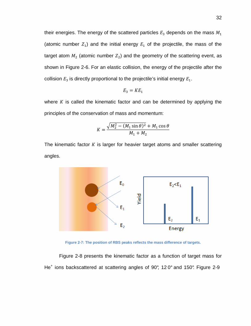
32
their energies. The energy of the scattered particles depends on the mass 7
(atomic number 4 ) and the initial energy of the projectile, the mass of the
target atom 7 (atomic number 4) and the geometry of the scattering event, as
shown in Figure 2-6. For an elastic collision, the energy of the projectile after the
collision is directly proportional to the projectile’s initial energy .
where is called the kinematic factor and can be determined by applying the
principles of the conservation of mass and momentum: 87 97 sin $; 7 cos $7 7
The kinematic factor is larger for heavier target atoms and smaller scattering
angles.
Figure 2-7: The position of RBS peaks reflects the mass difference of targets.
Figure 2-8 presents the kinematic factor as a function of target mass for
He+ ions backscattered at scattering angles of 90°, 12 0° and 150°. Figure 2-9

33
plots the kinematic factor for He+ ions backscattered from O, Al, Ge and Hf at
various scattering angles.
Figure 2-8: Kinematic factor for He+ ions backscatt ering from different masses at different scattering
angles.
Figure 2-9: Kinematic factor for He+ ions backscatt ering from different targets at different scatterin g
angles.
The projectile mass must be smaller than that of the target atom (7 <7) for backscattering to occur ($ 5 90°). In order to analyze a wide range of
target masses, light projectiles such as H+ and He+ ions are typically used in
backscattering experiments.

34
The ability of the backscattering system to distinguish between target
atoms with a mass difference =7, is determined by the ability of the system to
resolve energy differences = of backscattered particles. The mass resolution of
the system is given by =7 = ))7
Mass resolution can be improved by increasing the incident energy ,
using a larger projectile mass 7 , using scattering angles close to 180°, or by
improving the overall energy resolution, =.
2.2.2 Scattering Cross Section and Areal Density of Target Atoms
The probability >, that a particle will be backscattered from a sample with
areal density ? into the detector solid angle @, is given by the ratio of the
number of detected particles A (the yield), to the number of incident particles 2: > A2
The yield A of backscattered particles depends on the differential cross section.
By assuming the Coulomb force between the incident and target nuclei, an
unscreened Rutherford cross section may be calculated from the following:
)#9, $;)Ω D4 4+16F G 49sin $;! IJ1 K7 7sin $L cos $M
J1 K7 7sin $L

35
where is the energy of the ion immediately before scattering, + is the electronic
charge, and $ is the scattering angle. For small detector solid angles (@ < ~ 10
msr) and well defined scattering angles $, the differential cross section )#/)@ simplifies to #9, $; [13]: #9, $; P )#9, $;)Ω )Ω Q 4π )#9, $;)Ω
Actual cross sections can deviate from the Rutherford description if nuclear
reaction is involved or if the energy is low enough when electron screening of the
nucleus is important. Ion beam techniques are termed Nuclear Reaction Analysis
(NRA, 100 keV ~ 1 MeV) if nuclear reaction happens [14], Medium Energy Ion
Scattering (MEIS, 20~200 keV) if the beam energy is low enough such that the
cross sections deviate from an unscreened Rutherford value by more than about
one percent [15, 16], or Low Energy Ion scattering (LEIS, 500 eV ~ some keV) if
the Rutherford cross section totally breaks down [17].
The areal density 9?; (atoms/cm2) of the ith element with the physical
thickness can be determined with knowledge of #, @, the integrated peak count , and the total charge collected 2 by 9?; cos S2. #9, $;Ω
where S is the angle between the incident beam and target normal. The average
atomic ratio for a film containing compound AmBn can be calculated by taking the
ratio of atomic densities: !T 9?;9?; . #9, $;#9, $;

36
This equation can be used to calculate stoichiometric ratios without knowledge of
the quantities 2 and @. The uncertainty of average stoichiometric ratios
determined by this is a few tenths of 1% [18].
In the compound AmBn, the areal density 9?; of the ith element can be
converted to a physical film thickness if the mass density, U of the film AmBn
is known: 9?;? 9?;?
The atomic densities are defined as ? TU?7 ? !U?7
where ? is Avogadro’s number and 7 T7 !7 is the molecular weight
of compound AmBn. Areal densities obtained from the equation above have an
uncertainty of about ±3% [18].
2.2.3 Depth Profiling Using RBS
The energy losses of the incident particles that result when penetrating the
sample occur both along the incident path, before the main scattering event (with
energy loss V ) and after backscattering, along the exit path (with energy loss V). The energy loss process is due to many kinds of interactions between the
projectile ion, target nuclei, and target electrons [18], and can be viewed as an

37
average over all possible energy dissipative processes activated by the projectile
as it passes an atom [19]. The total energy loss V is ∆ ∆ ∆
The energy loss extracted from RBS spectra can be used to identify scattering
depth and provides a profile of target constituents.
Figure 2-10: The position of RBS peaks reflects the depth distribution of targets.
The amount of energy the ion loses per distance traveled in matter is
given by the stopping power of the material, which depends on the energy, the
charge and the mass of the ion as well as the material traversed. These
interactions are due only to electromagnetic forces and any energy lost to
nuclear reactions between the projectile and target nuclei can be ignored in RBS
[20].
The stopping cross section ε is the energy loss per unit areal density and
is related to the energy loss rate via the physical thickness traversed: 1? ))X

38
where ? is the atomic density in atoms/cm3 and )/)X is the stopping power. In
the low energy regime, the stopping cross section decreases because projectiles
may capture electrons from the target and partially neutralize their nuclear
charge. The stopping cross section decreases at higher energy because the
projectile with larger velocity spends less time in the vicinity of the atom [13].
An approximation called Bragg’s rule is used to determine the stopping of
ions in compounds. This approximation ignores the effects of chemical bonding
in the compound and assumes that each target atom independently contributes
to the energy loss process [19]. The compound stopping cross section in terms of
energy loss/molecule/cm2 traversed for a compound AmBn can be approximated
by T !
The energy loss V of ions traversing matter can be calculated by
integrating the stopping power )/)X over the distance travelled. For the case of
thin targets, the stopping power can usually be regarded as constant, so energy
loss can be approximated using the following: ∆ P ))X )X ?X9;
where is taken as either the initial beam energy, (surface energy
approximation), or the mean energy of the analysis ion over path length X (mean
energy approximation).

39
2.2.4 Channeling
The arrangement of atoms in single crystals plays an important role in
incident ion-target interactions [13]. When the ions enter a crystalline substrate
parallel to one of the crystal axes, the backscattering yield is greatly reduced
(~0.01x). The resulting spectrum is called a channeling spectrum. Channeling
analysis can be used, for example, to increase the sensitivity to light elements in
an amorphous overlayer film by channeling through the crystal substrate beneath
the film. By reducing the substrate signal, the signal from light elements
superimposed on the substrate signal is enhanced, and thus the sensitivity is
greatly improved. Channeling spectra can also be used to determine whether or
not the sample is crystalline. The percentage ratio of channeling yield A" and not
channeling (random) yield A# reflects the epitaxial growth quality.
Figure 2-11: Channeling is the guided motion of ion s in the open channels of a crystal target.
Figure 2-12 compares simulation of a random and a channeled
backscattering spectrum obtained from 270 keV He+ incident on native silicon

40
oxide on Si(100). The Si peak in the channeled spectrum is due to contributions
from the native oxide layer and from the first few monolayers of the Si substrate.
Figure 2-12: Random and channeled spectrum of 270 k eV He+ incident on 25Å SiO 2/Si along <111>
[21].
2.2.5 SIMNRA
In this study, the commercial software package SIMNRA [22] is used to
model RBS spectra. SIMNRA is a Microsoft Windows based program used to
simulate backscattering spectra for ion beam analysis with MeV ions. It can
calculate any ion-target combination including incident heavy ions and any
geometry including transmission geometry and arbitrary foils in front of the
detector. This calculation can give the atomic density ) of each layer constructed
in the stack model and then the physical film thickness , can be obtained with
the equation:

41
79T !;U?
where ? is Avogadro’s number, U is mass density and 7 T7 !7 is
the molecular weight of compound AmBn.
Section 2.3 AFM
Atomic force microscopy (AFM) is a type of scanning probe microscopy and
is useful for determining the topography of surfaces [23]. It uses a sharp probe to
scan across a surface while the interactions between the tip and the sample are
monitored.
2.3.1 Principle of AFM
Figure 2-13 shows the schematic drawing of typical commercial AFM
equipment. As the cantilever approaches the sample, the force between the
cantilever edge and the atoms of the sample surface cause the cantilever to
bend. The laser and photo diode are used to detect the bending of the cantilever
which gives information of the height of the tip 4 above the surface. The
cantilever is controlled by a z-direction feedback circuit while a topographic
image of the surface results from scanning in the x and y directions.

42
Figure 2-13: A schematic drawing of an AFM system.
There are three primary modes of operating an AFM: contact mode, non-
contact mode, and tapping mode. Tapping mode was used for this work. In
tapping mode, the cantilever is vibrated by a piezoelectric device, and the probe
makes only limited contact to the sample during part of the vibrational cycle.
Tapping mode often enables one to measure surface morphology with higher
resolution than the other modes, and minimizes damage done to the sample [24].
2.3.2 Quantification of Surface Roughness
To determine the roughness of a sample, an image of the surface is
obtained by scanning in the x and y directions. The surface roughness is
evaluated by the values of Y$% , the difference between the maximum and
minimum height values of the surface and the root mean square (RMS)

43
roughness. The standard deviation of the height values 4 within a given scan
area is given by: Y7' J∑ 4 4&'( ?
where 4&) is the average 4 value within the given area, 4 is the current 4 value,
and ? is the number of points within a given area.
AFM measurements should always be performed with high quality, durable,
sharp tips. Worn tips produce completely different images and the roughness
information obtained is not reliable. One should also take care to avoid multiple
tip imaging.
Section 2.4 FT-IR
Fourier transform infrared spectroscopy (FT-IR) [25] is an absorption
spectroscopy suitable for identifying chemical bonds by observing the
characteristic electromagnetic radiation absorbed by vibrating atoms in
molecules or solids in the infrared region.
2.4.1 Absorption Spectroscopy
Absorption spectroscopy is the study of absorption and transmission of
light energy in matter. The energy from the photons can be absorbed by
electronic, vibrational, or rotational transitions in molecules, corresponding to
44
electromagnetic radiation in ultraviolet, infrared and micro-wave to mm-wave
regions.
In absorption spectroscopy, the reference spectrum , is first measured
and another spectrum is obtained after a change of samples is made. The
transmittance which contains the information on the change of the sample is
defined as
When electromagnetic light is absorbed, the power of the transmitted energy
decreases exponentially with the path length. The relation between the fraction of
light intensity absorbed and the path length is given by: +
where ) is the path length and ’ is a constant. Transmittance also shows similar
dependence on the concentration of the absorbance: +"*
where ” is another constant. Combine these two equations with the definition of
absorbance as log to give Beer-Lambert law: log \)
The constant \ is known as absorptivity and is dependent on the wavelength and
fundamental physical properties of the molecules. A plot of the transmittance
versus wavenumber is called the transmittance spectrum and can be converted
into a absorbance spectrum.

45
2.4.2 Infrared Spectroscopy
When light interacts with matter, the vibrational mode of the chemical
bonds in the molecules changes if the vibrating dipole is in phase with the electric
vector of the incident radiation. Each chemical bond in a molecule vibrates at a
frequency which is characteristic of that bond. The vibrational frequencies of
most molecules correspond to the frequencies of infrared light. This is why
infrared (wavenumber of 4000–400 cm-1
) is usually used in vibrational
spectroscopy.
Only those vibrations that result in the change of the molecular, with
absorption frequencies in the infrared region, absorb infrared radiation. For
example, gas molecules such as H2 and O2 do not have dipoles and therefore do
not give infrared spectra.
The frequency of these vibrations depends on the mass of the atom and
the length and strength of the bonds because the bonds have to absorb radiation
of the same frequency as their natural vibrational frequency. For each molecule,
a variety of vibrations are possible and each corresponds to a different frequency
(Figure 2-14).

46
Figure 2-14: Some normal modes of –CH 2 molecular vibrations. The + and – symbols indicate a
movement out of and into the plane of the paper res pectively.
For a given bond or functional group, the absorption occurs within the
same wavenumber range regardless of the rest of the structure of the molecule.
For instance, the C=O stretch of a carbonyl group occurs at ~1700 cm-1 in
ketones, aldehydes and carboxylic acids. Therefore infrared absorption
spectroscopy is very useful for chemical identification.
2.4.3 FT-IR
Fourier Transform Infrared Spectroscopy (FT-IR) is based on absorption
spectroscopy with a significant improvement over traditional infrared
spectroscopy. In conventional infrared spectroscopy, the frequency of the
infrared light passing through samples is varied using a monochromator. The

47
amount of energy absorbed is recorded with one frequency at a time. In FT-IR,
the infrared light is guided through an interferometer and all the required
frequencies pass through the instrument at once. It is called FTIR spectroscopy
because a mathematical Fourier transformation is used to interpret the data and
produce a spectrum. The measured signals using an interferometer are called
interferograms. A Fourier transform is performed on the interferogram to obtain a
spectrum identical to that of conventional infrared spectroscopy, although with a
better signal to noise ratio for a given data collection time.
Figure 2-15: Schematic drawing of components of FT- IR and the Michelson interferometer.
Figure 2-15 shows a schematic drawing of an FT-IR spectrometer. A
Michelson Interferometer is built around the sample chamber. Radiation from an
infrared source is directed through the sample cell to a beam splitter. Half of the
infrared beam is reflected from a fixed mirror while the other half is reflected from
a mirror which moves continuously over a certain distance. Since the maximum
path difference of the two split beams determines the spectral resolution, the

48
longer the distance the moving mirror moves the better the resolution. When the
two beams are recombined at the detector, an interference pattern
(interferogram) is produced and stored in a computer. A helium-neon laser is
simultaneously directed through the Michelson Interferometer and the
interference pattern of the laser is used as a frequency reference.
FT-IR is cheaper, faster and more sensitive than conventional infrared
spectroscopy. It is cheaper because building a interferometer is easier than the
fabrication of a monochromator. In addition, measurement of a single spectrum is
faster for the FT-IR technique because the information at all frequencies is
collected simultaneously. Multiple scans can be collected and averaged together
resulting in an improvement in sensitivity. Because of these advantages, FT-IR
instruments are now used in most modern chemical laboratories.
In this work, the FT-IR measurements were done with the help of Prof.
Yves Chabal and his group members. The absorbance Fourier transform infrared
spectra were recorded at room temperature on a Nicolet FT-IR spectrometer [26]
with OMNIC software [27] at frequencies from 4000 to 400 cm-1
, with a resolution
of 4 cm-1
, gain = 1, and 100 to 500 scans.

49
Section 2.5 Reference
1. H. Hertz, On an effect of ultraviolet light upon electric discharge. Sitzungsber. d. Berl. Akad. d. Wiss., 1877.
2. A. Einstein, On a heuristic viewpoint concerning the production and transformation of light. Annalen der Physik, 1905. 17: p. 132.
3. H. Robinson and W.F. Rawlinson, Phil. Mag., 1914. 28: p. 277. 4. K. Siegbahn, Philosophical Transactions of the Royal Society of London Series A -
Mathematical and Physical Sciences, 1970. 268: p. 33. 5. K. Siegahn, C. Nordling, A. Fahlman, et al., Nova Acta Regiae Soc. Sci Upsaliensis, 1967:
p. 20. 6. L.C. Feldrnan and J.W. Mayer. Fundamentals of Surfce and Thin Film Analysis. 1986, New
York: North-Holland. 7. J.F. Moulder, W.F. Stickle, P.E. Sobol, et al., Hand Book X-ray Photoelectron
Spectroscopy. 2nd ed. 1992, Eden Prairie, MN: Perkin-Elmer Corp., Physical Electronics Division.
8. K. Siegbahn, C. Nordling, G. Johansson, et al., ESCA Applied to Free Molecules. 1969: North-Holland Publishing Company.
9. S. Oswald, B. Schmidt, and K.H. Heinig, Influence of sputtering conditions and electron energy on XPS depth profiling of Ge in SiO2. Crystal Research and Technology, 2005. 40(12): p. 1134-1138.
10. M.P. Seah, Surf. Interface Anal, 1986. 9: p. 85-98. 11. S. H¨ufner, Photoelectron Spectroscopy. 1996, Berlin: Springer-Verlag. 12. J.R. Bird and J.S. Williams, in Ion Beams for Materials Analysis. 1989, Academic Press. p.
104-106. 13. L.C. Feldman and J.W. Mayer, in Fundamentals of surface and thin film analysis. 1986,
Elsevier Science Publishing Co., Inc: New York. p. 352. 14. C.W. Magee, Nucl. Instr. and Meth., 1981. 191: p. 297. 15. R.A. Weller, in Methods in Materials Research. 2000, Wiley. p. 12b.1-15. 16. R.G. Smeenk, R.M. Tromp, H.H. Kerson, et al., Nucl. Instr. and Meth., 1982. 195: p. 581. 17. J.W. Rabalais, Principles and Applications of Ion Scattering Spectrometry: Surface
Chemical and Structural Analysis. 2003, New York: John Wiley & Sons, Inc. 18. J.A. Leavitt, L.C. McIntyre, and M.R. Weller, in Handbook of modern ion beam materials
analysis, J.R. Tesmer and M.A. Nastasi, Editors. 1995, Mater. Res. Soc.: Pittsburg. p. 5-19.
19. W.K. Chu, J.M. Mayer, and M.A. Nicolet, Backscattering Spectrometry. 1978, New York: Academic Press.
20. J.F. Ziegler, Stopping of energetic light Ions in elemental matter. Journal of Applied Physics, 1999. 85(3): p. 1249-1272.
21. R.D. Geil, Analysis of high-k dielectric thin films with time-of-flight medium energy backscattering. 2005, Vanderbilt University: Nashville, Tennessee.
22. M. Mayer. SIMNRA 6.0. Available from: http://www.rzg.mpg.de/~mam/. 23. C.R. Blanchard and J.B. Campbell, Atomic-force microscopy. Advanced Materials &
Processes, 1995. 148(2): p. 62-62. 24. D.A. Bonnell, in Scanning Probe Microscopy and Spectroscopy: Theory, Techniques, and
Applications. 2001, Wiley: New York. p. 493.

50
25. J. Sherma, Fourier transform infrared (FT-IR) spectrometry. Journal of Aoac International, 2004. 87(4): p. 113a-118a.
26. Nicolet. Nicolet FT-IR Spectrometer. Available from: http://www.thermo.com/com/cda/product/detail/0,1055,115542,00.html.
27. Thermo. OMNIC Software. Available from: http://www.thermo.com/com/cda/product/detail/0,1055,1000001344622,00.html.

51
Chapter 3 Preparation of Germanium Substrates
The cleanliness of germanium substrates is very crucial in the fabrication of
Ge-based MOSFET devices as it would be for any state of the art
semiconducting material. In addition to impurities, some oxides of Ge affect the
quality of high-k film growth as well as the electrical properties of the resulting
device. In this chapter, we compare the results of different wet chemical cleaning
methods and study surface passivation with hydrogen and sulfur in order to find a
better way to prepare Ge substrates for high-k ALD growth and subsequent
fabrication of high quality Ge-based MOSFETs.
Section 3.1 Cleaning of Germanium Substrates
The surface cleaning process has been one of the obstacles to film growth
on Ge. For Si and III-V substrates like GaAs, the procedures to prepare a clean
surface usually involve three steps: (1) degreasing, (2) chemical etching to
remove native oxide and other impurities and (3) growth of a protective oxide
layer (which is often removed, for example by annealing, in a controlled
environment right before the film growth) to ensure a clean substrate. However,
with the exception to the first step, which is usually performed with successive
ultrasonic baths in acetone and methanol, step 2 and 3 are quite challenging for
Ge. The removal of native oxides and other impurities from Ge substrates is not
as easy as it is for Si. The standard “RCA clean” method [1], commonly used on

52
Si, is not suitable on Ge because it is inefficient in removing carbon, the most
common impurity found on Ge, and it leaves noticeable marks on the surface.
Moreover, the formation of a non-permeable protective oxide layer on germanium
has been considered impractical because GeO2 has a high water-solubility (5.2
g/L) and can even be dissolved with moisture from air [2].
Many different wet-chemistry recipes have been utilized in order to remove
the native oxide layer and impurities from Ge surface. So far none of these
recipes has given satisfactory results [3-5] in the production of MOSFET quality
surfaces and many of them have resulted in significant residual carbon [4]. XPS
is a very useful technique to investigate the effects of different wet chemical
treatments on Ge surface; my XPS results are presented below. In this study, all
photoelectron peaks are fitted with a Gaussian band after the inelastic
background intensity is subtracted. In the following discussion, all Ge samples
are first degreased in ultrasonic baths of acetone and methanol, for 15 minutes
(each), and then different wet chemical treatments are applied. After each
treatment, the Ge samples are blown dry with nitrogen (N2) and analyzed.
3.1.1 Native Oxides
Figure 3-1 shows the XPS Ge 3d core-level spectrum of an as-received
Ge(100) sample and the number in parenthesis for each peak denotes the
corresponding chemical shift in eV. The major peak at 29 eV is responsible for
the elemental Ge originating from the substrate [3, 6, 7]. The peak at 32.5 eV,
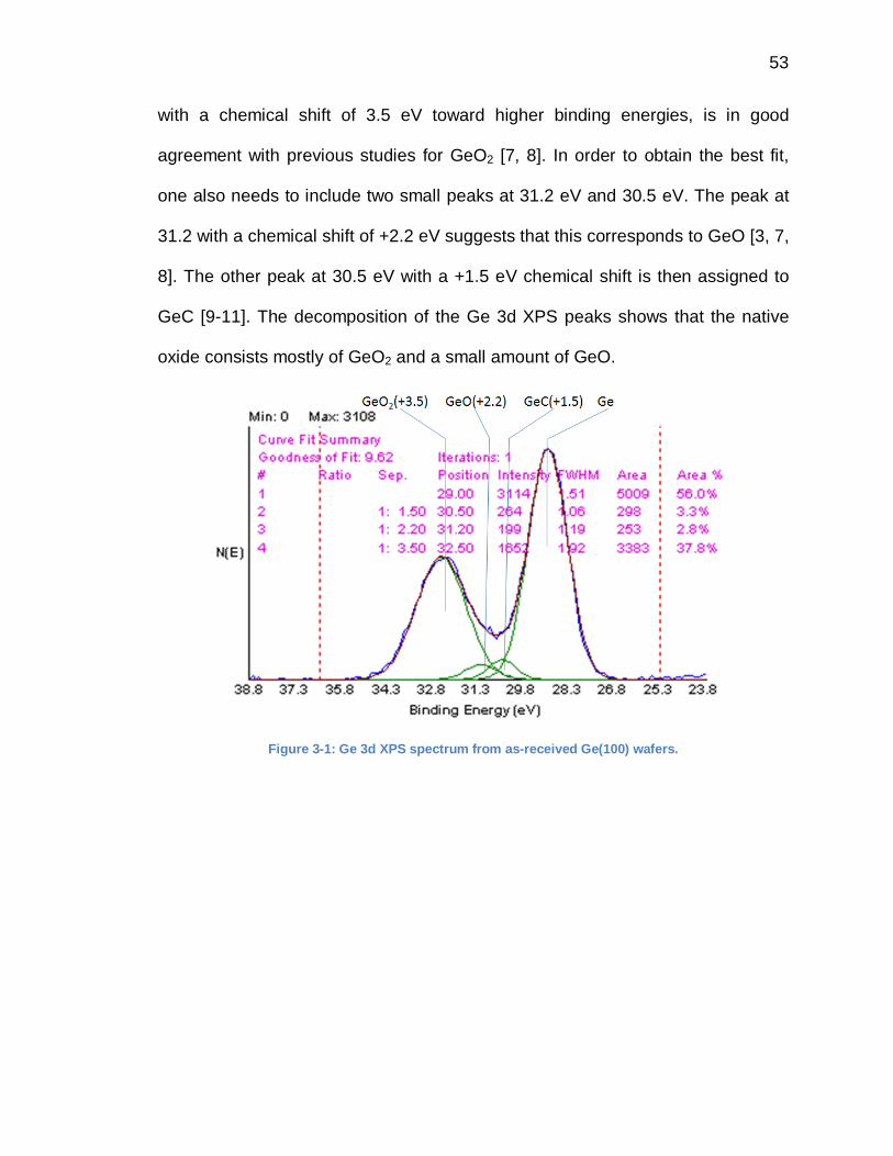
53
with a chemical shift of 3.5 eV toward higher binding energies, is in good
agreement with previous studies for GeO2 [7, 8]. In order to obtain the best fit,
one also needs to include two small peaks at 31.2 eV and 30.5 eV. The peak at
31.2 with a chemical shift of +2.2 eV suggests that this corresponds to GeO [3, 7,
8]. The other peak at 30.5 eV with a +1.5 eV chemical shift is then assigned to
GeC [9-11]. The decomposition of the Ge 3d XPS peaks shows that the native
oxide consists mostly of GeO2 and a small amount of GeO.
Figure 3-1: Ge 3d XPS spectrum from as-received Ge( 100) wafers.

54
Figure 3-2: Ge 3d XPS spectra of an as-received Ge( 100) sample at different take-off angles.
The thickness of the native oxide is determined by angular resolved
photoelectron spectroscopy (ARPES) as discussed above in Section 2.1. Figure
3-2 shows a set of Ge 3d XPS spectra at different photoelectron take-off angles.
The small take-off angle measurements detect the photoelectron originating from
the surface. Therefore, the peak intensity ratio of the overlayer to the substrate
becomes larger when the take-off angle decreases. The thickness of the
overlayer can be calculated from this ratio and the take-off angle as shown in
Section 2.1.3. For simplicity, one can assume that the oxide overlayer consists
only of GeO2 because the amount of GeO and GeC is much less than that of
GeO2. In the calculation, the inelastic mean free path & of Ge 3d photoelectrons
in GeO2 is 3.3 nm, which is the average of the reported experimental values [3,
12, 13]. The calculated thickness of the native oxide is 1.53 nm on Ge(100)

55
(Figure 3-3), and 2.75 nm on Ge(111) (not shown) which are in good agreement
with the previous studies: 1.8 nm on Ge(100) [3, 10] and 2-3 nm on Ge(111) [14].
Figure 3-3: Calculation of the thickness of the oxi de overlayer on Ge(100).
3.1.2 Removal of Native Oxide and Carbon
Because water is often present in chemical solutions and GeO2 has a high
water-solubility, the effects of water on a Ge surface need to be well understood.
A degreased Ge sample was rinsed with running de-ionized water (DIW, 18.2
MΩ cm) for 1 minute and then blow-dried with N2 before being loaded into the
XPS chamber. The Ge 3d XPS spectrum in Figure 3-4 shows that the GeO2
component completely disappears due to the DIW rinse. This implies that the
majority of the Ge native oxide must be either amorphous or hexagonal GeO2
which are both highly water-soluble but not the insoluble tetrahedral specie [2].

56
However, the two small GeO and GeC peaks are still present and the DIW rinse
alone cannot remove all of the germanium sub-oxide and carbides.
Figure 3-4: Ge 3d XPS spectrum from a Ge(100) wafer after DIW rinsing.
Hydrofluoric acid (HF) is often used to etch the native oxide layer and
produce hydrogen terminated surfaces on Si and Ge wafers. The use of
concentrated HF acid solutions (49%) on Ge should be avoided because such
concentrated HF solutions increase the roughness of the surface [15, 16] without
further decreasing the amount of sub-oxide [17]. The formation of the rougher
surface is due to the Ge back-bond breaking during HF etching [15]. To reduce
this effect, HF is diluted to a concentration of 2% to 10% with either DIW or
hydrogen peroxide (H2O2). It has been determined that cyclic HF/DIW rinses are
effective in removing the native oxide [14]. For the treatment of cyclic HF/DIW
rinses, Ge samples are rinsed in DIW, dipped in HF acid solution and rinsed in
DIW again. This procedure is repeated for 3 to 5 times in order to peel off the
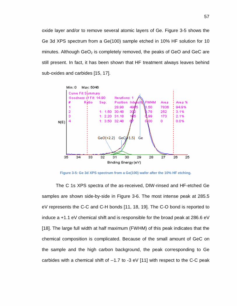
57
oxide layer and/or to remove several atomic layers of Ge. Figure 3-5 shows the
Ge 3d XPS spectrum from a Ge(100) sample etched in 10% HF solution for 10
minutes. Although GeO2 is completely removed, the peaks of GeO and GeC are
still present. In fact, it has been shown that HF treatment always leaves behind
sub-oxides and carbides [15, 17].
Figure 3-5: Ge 3d XPS spectrum from a Ge(100) wafer after the 10% HF etching.
The C 1s XPS spectra of the as-received, DIW-rinsed and HF-etched Ge
samples are shown side-by-side in Figure 3-6. The most intense peak at 285.5
eV represents the C-C and C-H bonds [11, 18, 19]. The C-O bond is reported to
induce a +1.1 eV chemical shift and is responsible for the broad peak at 286.6 eV
[18]. The large full width at half maximum (FWHM) of this peak indicates that the
chemical composition is complicated. Because of the small amount of GeC on
the sample and the high carbon background, the peak corresponding to Ge
carbides with a chemical shift of --1.7 to -3 eV [11] with respect to the C-C peak

58
is not observed. However, this does not imply the absence of Ge carbides. The C
1s peaks are reduced on both the DIW-rinsed and HF-etched sample. This is
because when GeO2 is removed, the hydrocarbon trapped inside is also
removed from the surface.
Figure 3-6: C 1s XPS spectra from as-received, DIW- rinsed and HF-etched Ge(100) samples.
Other common chemicals used to etch the Ge native oxide include
ammonia (NH4OH), hydrochloric acid (HCl), and sulfuric acid (H2SO4). The
advantage of NH4OH and HCl is the preservation of the original
morphology/roughness [16, 20, 21]. A very uniform surface can be attained by a
5-minute NH4OH (27%) etch because NH4OH has a slow etching rate of which is
even slower than DIW [16, 21]. Concentrated HCl (20%) is more effective at
remove metal contamination than HF (2-20%) [17], but HCl-treated surfaces
attract more contaminants than HF-treated ones [15]. A diluted H2SO4 solution
(H2SO4:DIW = 1:7) is reported to remove metals as well as hydrocarbons

59
effectively [21]. However, none of these etch processes alone can lead to an
oxygen and carbon free surface without further vacuum annealing [15].
Figure 3-7: Ge 3d XPS spectra as a function of anne aling temperature [22].
Vacuum annealing is a common cleaning method to desorb oxygen and
carbon from the surface. However, even with annealing in UHV, to obtain a
smooth sub-oxides- and carbides-free Ge surface is not as easy as it is for Si.
Figure 3-7 shows Ge 3d XPS spectra as a function of annealing temperature. As
the annealing temperature is raised, the amount of GeO2 decreases and the
amount of GeO increases. This suggests the occurrence of the following surface
transformation: GeO2 + Ge → GeO [7, 8, 22, 23]. Even though the oxygen is
totally removed after vacuum annealing at 450-480 °C for 30 minutes, there is
always some carbon left on the surface from XPS [3, 15], AES (Auger Electron
Spectroscopy) and EELS (Electron Energy Lose Spectroscopy) [3] studies.

60
3.1.3 Protective Chemical Oxides
Since it is difficult to completely remove oxide and carbon from Ge
substrates, different approaches involving the transformation of these into other
chemical species which are easier to remove have been investigated, for
example: (1) GeO → GeO2 and (2) GeC → CO2 [3, 16, 21, 24]. This is usually
done with either UV/ozone or wet chemical oxidation. In UV/ozone oxidation,
degreased Ge samples are first rinsed with DIW to remove GeO2 and then
oxidized in the presence of ozone, produced from an ultraviolet (UV) lamp, in
either a vacuum chamber or a closed oxygen-purging box [3, 24]. The thickness
of the oxides formed by UV/ozone is reported to be 1 nm [24] to 1.8 nm [3]
determined by angular resolved photoelectron spectroscopy (ARPES). XPS
spectra show that the complete oxide desorption takes place after a vacuum
annealing at 350 °C for 30 minutes and C 1s, O 1s and chemically shifted Ge 3d
oxide peaks are not detectable resulting in a clean Ge surface (Figure 3-8).

61
Figure 3-8: C 1s (left) and O 1s (right) XPS spectr a from Ge(100) after UV/ozone exposure and
annealing [3].
H2O2 is often used in wet chemical oxidation on a Ge surface. Since H2O2
usually contains some impurities, including organic compounds, H2O2 should be
diluted with either a base or an acid [25]. Okumura has compared the oxidation
effect on Ge using H2O2/H2O (1/10) and NH4OH/H2O2/H2O (0.5/1/10) [16]. It is
shown that no protective oxide can be formed with H2O2 solution diluted in H2O
(H2O2:H2O=1:10) because water etches the chemical oxide. On the other hand
with the addition of NH4OH, chemical oxide remains due to the slower etching
rate of NH4OH than that of DIW. In this work, we have compared chemical oxides
formed by concentrated H2O2 and a mixture of H2SO4/H2O2 (4/1). The reasons
for using H2SO4 with H2O2 for oxidation are: (1) H2SO4 helps remove
hydrocarbon [21] and (2) the oxidation in the acid-base reaction is stronger and
more effective in converting GeO and GeC. Degreased Ge samples were first
rinsed in DIW to remove GeO2 and then dipped into either concentrated H2O2 or

62
a mixture of H2SO4/H2O2 (4/1) for 10 minutes. The Ge 3d XPS spectra from the
Ge samples with chemical oxides formed by these two solutions are shown in
Figure 3-9 and Figure 3-10.
Figure 3-9: Ge 3d XPS spectrum from a Ge(100) sampl e with a chemical oxide formed by
concentrated H 2O2.
Comparing Figure 3-9 and Figure 3-10, GeO signals are not detectable
and the intensities of the GeC peaks are small. One of the major differences
between these two methods is the thickness of the chemical GeO2 layer. ARPES
has been performed to determine the thickness of the chemical oxides in each
case. While the thickness of the GeO2 layer formed by the concentrated H2O2 is
2.1 nm, compared to 1.9 nm reported in the previous studies [16, 21], the
H2SO4/H2O2 mixture grows a much thicker GeO2 layer (~12.4 nm). Another
difference is the amount of remaining carbon on the surface. The intensity of the
C 1s peak, from a cyclic HF/DIW/H2O2 treated Ge sample, is still ~38% larger
compared to that of a H2SO4/H2O2 treated sample.

63
Figure 3-10: Ge 3d XPS spectrum from a Ge(100) samp le with chemical oxide formed by H 2SO4/H2O2.
The comparisons of the C 1s peaks from the Ge samples undergoing
different wet chemical cleaning methods are shown in Figure 3-11. The
H2SO4/H2O2-treated Ge samples appear to contain the least amount of carbon.
Figure 3-11: Comparison of C 1s XPS peaks with diff erent cleaning methods.

64
The formation of a chemical oxide not only reduces the amount of carbon
on the Ge surface but also helps protect the surface from further carbon
contamination. Figure 3-12 shows C 1s XPS spectra from two sets of Ge
samples which have a chemical oxide formed on the surface using two different
treatments: cyclic HF/DIW/H2O2 and H2SO4/H2O2. If the chemical oxide is
removed either by a DIW rinse or by HF etching, the intensity of the C 1s peak
will increase. Interestingly, after the chemical oxides are removed, the intensity of
the C 1s peak from the H2SO4/H2O2-treated Ge sample increases much more
(~120%) than that from the cyclic HF/DIW/H2O2 rinsed sample (26%). This is
most likely due to H2SO4/H2O2 oxidation removing more carbon from the Ge
surface than cyclic HF/DIW/H2O2 rinses. Once the protective oxide is removed,
the amount of carbon increases to the same saturated level due to environmental
contamination.
Figure 3-12: Intensity changes of C 1s XPS peaks be fore and after the removal of chemical oxide.

65
Figure 3-13: Etching and chemical oxidization on as -received Ge wafers.
Section 3.2 Passivation on Germanium Substrates
In this work, two different methods of passivating Ge substrates have been
investigated: hydrogen-termination and sulfur passivation. Both of these methods
are accomplished with wet chemistry, because it is more desirable in industry for
the simplicity of this method, as well as its lower cost. Hydrogen terminated Ge
surface produced by HF etch cleaning is studied as a comparison to sulfur
passivation which is reported to be more stable in ambient [26].

66
3.2.1 Passivation with Hydrogen
A hydrogen-terminated Ge surface can be prepared in an HF solution [14,
27]. Fourier Transform Infrared Spectroscopy (FT-IR) is a useful technique to
study the formation of H-Ge as well as the quality of the H-terminated surface.
Figure 3-14: FT-IR spectra of a H-terminated Ge(100 ) sample (blue) vs. H 2SO4/H2O2-treated Ge
sample followed by a DIW rise (red) using as-receiv ed Ge samples as a reference.
After two H2SO4/H2O2-oxidized Ge samples were prepared, one of them
was etched with dilute HF (10%) for 10 minutes to produce a hydrogen-
terminated surface and the other was rinsed with DIW to remove the chemical
oxide. The FT-IR spectra using as-received samples as a reference are shown in
Figure 3-14. A strong negative feature appears between 750 and 1050 cm-1,
corresponding to the removal of the Ge oxides. The three downward peaks in
67
this region are assigned to the LO and TO phonon modes of GeO2 and the Ge=O
stretch (980 cm-1) [10]. The significant overlap of these two spectra implies that
the chemical oxide formed after H2SO4/H2O2 must be soluble GeO2 so that a
DIW rinse can produce the same effect as the HF etch. This FT-IR result shows
that H2SO4/H2O2 oxidation, together with HF etches or a DIW rinse, can
effectively remove GeO2 and GeO from the as-received Ge surface and is in
good agreement with the previous XPS studies from Section 3.1. The positive
peak around 2030 cm-1 confirms the formation of an H-terminated surface.
However, the broadness and asymmetry of this absorbance band resulting from
the stretching vibration of H-Ge, H2-Ge and H3-Ge implies that the H-terminated
surface is atomically rough [10, 27].
To further understand the advantage of H2SO4/H2O2 oxidation on the Ge
surface, H-terminated Ge samples were prepared with different cleaning
methods: cyclic DIW/HF and H2O2 rinses. The comparison of absorbance FT-IR
spectra is plotted in Figure 3-15. After 10 minutes in dilute HF, all three spectra
show strong negative features between 750 and 1050 cm-1 corresponding to the
removal of the Ge oxide. The downward peaks in the range of 1350-1550 cm-1
reflect the absence of hydrocarbon and only appear for H2SO4/H2O2- and H2O2-
treated samples. Therefore, chemical oxidation methods with either H2SO4/H2O2
or H2O2 prove to be more effective in removing hydrocarbon from the as-received
Ge surface than the cyclic DIW/HF rinses. Comparison of the integrated area
shows that H2SO4/H2O2 removes more hydrocarbon than H2O2 alone. The
positive peak around 2030 cm-1 is due to the Hx-Ge stretching vibration. In our

68
study, the Hx-Ge peak only appears on the HF-etched Ge samples with prior
H2SO4/H2O2 oxidation. This suggests that how the Ge surface is cleaned
determines the amount of remaining hydrocarbon on the surface and therefore
affects the formation of H-Ge bonds.
Figure 3-15: FT-IR spectra of HF-etched Ge(100) aft er a different wet chemical cleaning is applied.
Successive FT-IR spectra were taken in order to study the stability of an
H-terminated Ge(100) surface both in air and in N2 (Figure 3-16). Nearly all Hx-
Ge bonds are removed in the first 100 minutes in air, and therefore the H-
terminated surface is very unstable which has also been observed in a previous
study [26]. In the N2 environment, the H-terminated surface can be preserved for
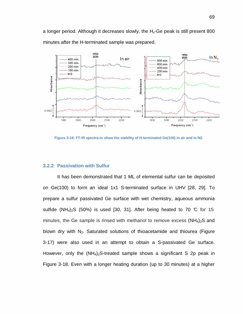
69
a longer period. Although it decreases slowly, the Hx-Ge peak is still present 800
minutes after the H-terminated sample was prepared.
Figure 3-16: FT-IR spectra to show the stability of H-terminated Ge(100) in air and in N2.
3.2.2 Passivation with Sulfur
It has been demonstrated that 1 ML of elemental sulfur can be deposited
on Ge(100) to form an ideal 1x1 S-terminated surface in UHV [28, 29]. To
prepare a sulfur passivated Ge surface with wet chemistry, aqueous ammonia
sulfide (NH4)2S (50%) is used [30, 31]. After being heated to 70 °C for 15
minutes, the Ge sample is rinsed with methanol to remove excess (NH4)2S and
blown dry with N2. Saturated solutions of thioacetamide and thiourea (Figure
3-17) were also used in an attempt to obtain a S-passivated Ge surface.
However, only the (NH4)2S-treated sample shows a significant S 2p peak in
Figure 3-18. Even with a longer heating duration (up to 30 minutes) at a higher

70
temperature (100 °C ), neither thioacetamide nor thiourea can produce S-
passivated Ge surfaces.
Figure 3-17: Molecular structure of thioacetamide a nd thiourea.
Figure 3-18: S 2p XPS spectra from Ge(100) treated in (NH4)2S, thioacetamide and thiourea solution.
In our study, Ge samples which are later used for high-k ALD growth in
Ge-based MOSFETs are first pretreated with H2SO4/H2O2 to remove the native
oxide and grow a protective chemical oxide, and then heated in a (NH4)2S
solution to form a sulfur passivation layer on the surface. The advantages of
doing so will become clear later in this section. Figure 3-19 shows Ge 3d XPS
spectrum of a Ge sample which has undergone such a treatment. Two major
differences are observed in Figure 3-19 when comparing the Ge 3d spectrum

71
from a H2SO4/H2O2-treated sample. First, the peak with a 3 eV chemical shift
corresponding to GeO2 disappears which implies that the chemical oxide is
completely removed by a hot aqueous (NH4)2S solution. Second, a broad peak
with a chemical shift of 0.66 eV is present due to the surface Ge atoms bonded
to S atoms. In previous studies, this has been attributed to one layer of bridge-
bonded S atoms on the Ge surface [28, 29].
Figure 3-19: Ge 3d XPS spectrum from a (NH 4)2S-treated Ge(100) sample.
Because the mean-free-path associated with the Ge 2p core-level
photoelectrons is smaller, the Ge 2p peak is more sensitive to the surface
change than the Ge 3d peak. Therefore, the Ge 2p region of XPS spectra is used
to study the removal of Ge oxides and the change of chemical states on the
surface. Figure 3-20 shows the Ge 2p XPS spectra from the same S-passivated
Ge sample. In the inset in the lower right corner of Figure 3-20, a Ge 2p
spectrum of the S-passivated Ge sample is compared to that of an as-received

72
sample. The GeO2 peak disappears after the successive wet chemical
treatments in H2SO4/H2O2 and (NH4)2S. The numerical deconvolution of the Ge
2p peak shows that three peaks with non-zero chemical shifts exist in addition to
the elemental Ge in the bulk. The one with the largest chemical shift (+2.8 eV) is
due to GeO2 [26] and accounts for 2.5% of the total integrated peak area.
Because of the strong S 2p peak (Figure 3-18) and the negligible O 1s peak (not
shown), the other two peaks which have smaller chemical shifts must correspond
to Ge atoms that are bonded to S atoms on the surface. According to Weser,
each S-Ge bond induces a chemical shift of 0.33 eV in the binding energy of Ge
2p photoelectrons [28]. Therefore, these two peaks with chemical shifts of +0.66
and +1.28 eV are assigned to the doubly sulfur coordinated Ge (GeS) and the
quadruply sulfur coordinated Ge (GeS2) respectively. The thickness of the sulfur
passivation layer is estimated to be 0.16 nm with ARPES and indicates that
about a monolayer of S has been formed on the Ge surface. The mean free path
of Ge 2p photoelectrons in GeS2, & 0.51 nm [28], was used in the calculation.
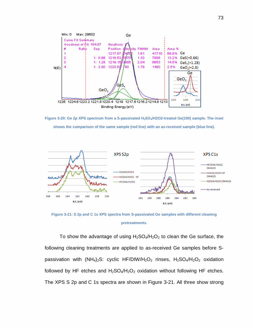
73
Figure 3-20: Ge 2p XPS spectrum from a S-passivated H2SO4/H2O2-treated Ge(100) sample. The inset
shows the comparison of the same sample (red line) with an as-received sample (blue line).
Figure 3-21: S 2p and C 1s XPS spectra from S-passi vated Ge samples with different cleaning
pretreatments.
To show the advantage of using H2SO4/H2O2 to clean the Ge surface, the
following cleaning treatments are applied to as-received Ge samples before S-
passivation with (NH4)2S: cyclic HF/DIW/H2O2 rinses, H2SO4/H2O2 oxidation
followed by HF etches and H2SO4/H2O2 oxidation without following HF etches.
The XPS S 2p and C 1s spectra are shown in Figure 3-21. All three show strong
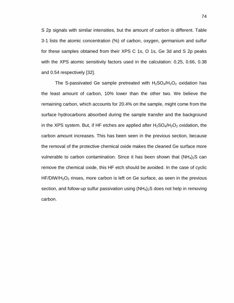
74
S 2p signals with similar intensities, but the amount of carbon is different. Table
3-1 lists the atomic concentration (%) of carbon, oxygen, germanium and sulfur
for these samples obtained from their XPS C 1s, O 1s, Ge 3d and S 2p peaks
with the XPS atomic sensitivity factors used in the calculation: 0.25, 0.66, 0.38
and 0.54 respectively [32].
The S-passivated Ge sample pretreated with H2SO4/H2O2 oxidation has
the least amount of carbon, 10% lower than the other two. We believe the
remaining carbon, which accounts for 20.4% on the sample, might come from the
surface hydrocarbons absorbed during the sample transfer and the background
in the XPS system. But, if HF etches are applied after H2SO4/H2O2 oxidation, the
carbon amount increases. This has been seen in the previous section, because
the removal of the protective chemical oxide makes the cleaned Ge surface more
vulnerable to carbon contamination. Since it has been shown that (NH4)2S can
remove the chemical oxide, this HF etch should be avoided. In the case of cyclic
HF/DIW/H2O2 rinses, more carbon is left on Ge surface, as seen in the previous
section, and follow-up sulfur passivation using (NH4)2S does not help in removing
carbon.

75
Table 3-1: Comparison of XPS atomic concentration ( %) of S-passivated samples with different
cleaning.
In this chapter, we have demonstrated that H2SO4/H2O2 oxidation is the
best method to remove the native oxides and reduce the Ge carbides from an as-
received Ge surface because of its strong oxidation. It also forms a thick
protective chemical oxide, mainly GeO2, on the surface to prevent further carbon
contamination. Sulfur passivation using hot (NH4)2S solution not only removes
this chemical oxide but also forms about one ML of S/Ge which helps passivate
the Ge surface. These two wet chemical treatments together prepare a clean S-
passivated Ge substrate for high-k ALD and fabrication of Ge-based MOSFETs.

76
Section 3.3 Reference
1. W. Kern and D.A. Puotinen, RCA Rev, 1970. 31: p. 197. 2. J.C. Bailar, H.J. Emeieus, and R. Nyholm, Comprehensive inorganic chemistry. Vol. 2.
1973, Pergamon, Oxford: Elsevier. 3. X.-J. Zhang, G. Xue, A. Agarwal, et al., Thermal desorption of ultraviolet–ozone oxidized
Ge(001) for substrate cleaning. The Journal of Vacuum Science and Technology A, 1993. 11: p. 2553.
4. D.A. Kiewit, I.J. d'Haenens, and J.A. Roth, Germanium surface cleaning—an Auger analysis. Journal of The Electrochemical Society, 1974. 121: p. 310.
5. K. Prabhakarana, T. Ogino, R. Hull, et al., An efficient method for cleaning Ge(100) surface. Surface Science, 1994. 316(1-2): p. L1031-L1033.
6. T.-C. Chiang, Core-level photoemission studies of surfaces, interfaces, and overlayers. Critical Reviews in Solid State and Materials Sciences, 1988. 14(3): p. 269.
7. K. Prabhakaran and T. Ogino, Oxidation of Ge(100) and Ge(111) Surfaces - an Ups and Xps Study. Surface Science, 1995. 325(3): p. 263-271.
8. D. Schmeisser, R.D. Schnell, and F.J.H. A. Bogen, D. Rieger, G. Landgren and J. F. Morar, Surface oxidation states of germanium. Surface Science, 1986. 172(2): p. 455.
9. J. Vilcarromero and F.C. Marques, XPS study of the chemical bonding in hydrogenated amorphous germanium-carbon alloys. Applied Physics a-Materials Science & Processing, 2000. 70(5): p. 581-585.
10. S. Rivillon, Y.J. Chabal, F. Amy, et al., Hydrogen passivation of germanium (100) surface using wet chemical preparation. Applied Physics Letters, 2005. 87(25): p. -.
11. C.Q. Hu, W.T. Zheng, H.W. Tian, et al., Effects of the chemical bonding on the optical and mechanical properties for germanium carbide films used as antireflection and protection coating of ZnS windows. Journal of Physics-Condensed Matter, 2006. 18(17): p. 4231-4241.
12. J. Szajman, J.G. Jenkins, J. Liesegang, et al., Journal of Electron Spectroscopy and Related Phenomena, 1978. 14: p. 41.
13. H. Gant and W. Monch, Electron escape depths in germanium. Surface Science, 1981. 105(1): p. 217.
14. T. Deegan and G. Hughes, An X-ray photoelectron spectroscopy study of the HF etching of native oxides on Ge(111) and Ge(100) surfaces. Applied Surface Science, 1998. 123: p. 66-70.
15. S.Y. Sun, Y. Sun, Z. Liu, et al., Surface termination and roughness of Ge(100) cleaned by HF and HCl solutions. Applied Physics Letters, 2006. 88(2): p. -.
16. H. Okumura, T. Akane, and S. Matsumoto, Carbon contamination free Ge(100) surface cleaning for MBE. Applied Surface Science, 1998. 125(1): p. 125-128.
17. J. Kim, S. Liu, S. Tan, et al., Germanium surface cleaning with hydrochloric acid. ECS Transactions, 2006. 3(7): p. 1191.
18. Y.J. Zhu, N. Olson, and T.P. Beebe, Surface chemical characterization of 2.5-mu m particulates (PM2.5) from air pollution in salt lake city using TOF-SIMS, XPS, and FTIR. Environmental Science & Technology, 2001. 35(15): p. 3113-3121.
19. P. Benzi, E. Bottizzo, C. Demaria, et al., Amorphous nonstoichiometric Ge1-x-C-x : H compounds obtained by radiolysis-chemical vapor deposition of germane/ethyne or germane/allene systems: A bonding and microstructure investigation performed by x-ray

77
photoelectron spectroscopy and Raman spectroscopy. Journal of Applied Physics, 2007. 101(12): p. -.
20. T. Akane, J. Tanaka, H. Okumura, et al., Preparation of high-quality Ge substrate for MBE. Applied Surface Science, 1997. 108(2): p. 303-305.
21. T. Akane, H. Okumura, J. Tanaka, et al., New Ge substrate cleaning method for Si1-x-yGexCy MOMBE growth. Thin Solid Films, 1997. 294(1-2): p. 153-156.
22. K. Prabhakaran, F. Maeda, Y. Watanabe, et al., Distinctly different thermal decomposition pathways of ultrathin oxide layer on Ge and Si surfaces. Applied Physics Letters, 2000. 76(16): p. 2244-2246.
23. K. Prabhakaran, F. Maeda, Y. Watanabe, et al., Thermal decomposition pathway of Ge and Si oxides: observation of a distinct difference. Thin Solid Films, 2000. 369(1-2): p. 289-292.
24. S. Gan, L. Li, T. Nguyen, et al., Scanning tunneling microscopy of chemically cleaned germanium (100) surfaces. Surface Science, 1998. 395(1): p. 69-74.
25. C.H. Bjorkman, H. Nishimura, T. Yamazaki, et al. Ultraclean semiconductor processing technology and surface chemical and passivation. in Material Research Society Symposium Proceedings. 1995. Pittsburgh, PA.
26. D. Bodlaki, H. Yamamoto, D.H. Waldeck, et al., Ambient stability of chemically passivated germanium interfaces. Surface Science, 2003. 543(1-3): p. 63-74.
27. K. Choi and J.M. Buriak, Hydrogermylation of alkenes and alkynes on hydride-terminated Ge(100) surfaces. Langmuir, 2000. 16(20): p. 7737-7741.
28. T. Weser, A. Bogen, B. Konrad, et al., Photoemission surface core-level study of sulfur adsorption on Ge(100) Physics Review B, 1987. 35(15): p. 8184.
29. T. Weser, A. Bogen, B. Konrad, et al., Chemisorption of sulfur on Ge(100). Surface Science, 1988. 201(1-2): p. 245.
30. G.W. Anderson, M.C. Hanf, P.R. Norton, et al., The S-Passivation of Ge(100)-(1x1). Applied Physics Letters, 1995. 66(9): p. 1123-1125.
31. T. Maeda, S. Takagi, T. Ohnishi, et al., Sulfur passivation of Ge (001) surfaces and its effects on Schottky barrier contact. Materials Science in Semiconductor Processing, 2006. 9(4-5): p. 706-710.
32. J.F. Moulder, W.F. Stickle, P.E. Sobol, et al., Hand Book X-ray Photoelectron Spectroscopy. 2nd ed. 1992, Eden Prairie, MN: Perkin-Elmer Corp., Physical Electronics Division.

78
Chapter 4 Atomic Layer Deposition of High-k Dielect rics
Because of its ability to control the thickness and conformality of deposited
films (in principle to the monolayer level), atomic layer deposition is the main
method used in this work to deposit thin films of high-k dielectrics on Ge and
other seminconductor substrates. In this chapter, the criteria of choosing
appropriate precursors are presented together with the experimental results from
the films deposited in our home-made ALD system.
Section 4.1 Atomic Layer Deposition
Atomic Layer Deposition (ALD) technology, originally known as Atomic
Layer Epitaxy (ALE), was developed and patented by Finnish researchers
Suntola and Antson in the middle of 1970s for the fabrication of thin film
electroluminescence (TFEL) displays where high quality insulating and
luminescent films on large area substrates were required [1]. Today, ALD has
become a useful tool in microelectronics for high permittivity (high-k) film growth
for CMOS devices and dynamic random access memory (DRAM) capacitors, as
well as for ferroelectrics, barrier materials, conductors such as metal gates [2, 3],
catalysis, magnetic recording head technology, and protective and antireflective
coatings [4].
79
4.1.1 Advantages of ALD Processes
The ALD processes and their applications have been frequently reviewed
[5-9], recently by Puurunen [10, 11], as well as by Ritala and Leskelä [4].
Different from chemical vapor deposition (CVD) and physical vapor deposition
(PVD), ALD is based on sequential and saturating surface reactions of the
alternately applied precursors. To minimize gas phase reactions between the two
precursor pulses, the precursor pulses are separated by inert gas purging and/or
by evacuation of the reaction chamber. The growth in a cyclic manner easily
enables thickness control and makes the film growth rate directly proportional to
the number of reaction cycles instead of the reactant concentration or time of
growth as in CVD and PVD.

80
Figure 4-1: Schematic drawing of one ALD cycle (ada pted from [12]).
In Figure 4-1, one simplified ALD cycle of a metal oxide deposition is
shown to illustrate the principle of ALD. The substrate surface is first exposed to
the vapor of a metal precursor and is saturated with the metal precursor on the
available surface sites (assumed to be –OH groups) through chemisorption (a).
After inert gas purging (here N2) or evacuation to remove the excess precursor
and ligand-exchange by-products (b), the surface is then exposed to the oxygen
source (here H2O) (c). The surface reaction produces the desired oxide film and
is ready for the next ALD cycle after inert gas purging or evacuation of excess
precursor and ligand-exchange by-products (d).

81
Figure 4-2: Different types of growth rate vs. prec ursor pulse time at a constant temperature [12].
The adsorption reaction in ALD of the precursors is a self-limiting process.
The amount of deposited precursor molecules on the substrate surface is
determined only by the number of reactive sites and is independent of the
precursor exposure after the surface becomes saturated with the precursor. By
working at a relatively low temperature, the precursor decomposition leading to a
CVD-type growth mode can be avoided, the adsorption designed to saturate at a
fractional monolayer, and the growth rate should then be independent of the
precursor dose, assuming saturation (Figure 4-2). Ideally, the maximum growth
rate is exactly one atomic layer per cycle. However, in most cases, the growth
rate is a fraction of a monolayer (ML) due to steric hindrance by the absorbed
precursor molecules and possibly by a limitation in the number of reactive
surface sites (Figure 4-3). As the growth proceeds in a cyclic manner and the
purging periods take some time, the ALD technique is rather slow compared to

82
CVD and PVD. In the application of ultrathin-film depositions, this is not a critical
issue, although for films thicker than 10 nm, it may limit production speed.
Figure 4-3: Factors that prevent full surface cover age of chemisorption: (a) steric hindrance of the
ligands, and (b) number of reactive surface sites [ 10].
Another advantage of ALD is that the deposition can be performed at
lower substrate temperatures. Since the adsorption of the precursor to the
surface is mainly thermally driven, a so-called ALD temperature window with a
constant deposition rate is usually observed [7, 13]. The substrate temperature
must be high enough to prevent condensation of any of the reactants and to
provide sufficient reactivity of the precursor. If condensation occurs during an
ALD cycle, undesirable or uncontrollable reactions may occur during the second
half cycle, resulting in the formation of porous and impure films. Therefore, a
minimum substrate temperature is also required to proceed with the ALD
process. There also exists a maximum substrate temperature for ALD. If the
temperature is too high, the undesirable decomposition of a reactant may occur
and CVD reactions will result, leading to rapid, uncontrolled deposition of a film.

83
Desorption of the precursor may also become more likely at higher temperatures
and can result in a decreasing growth rate versus temperature. The ALD window
is not a requirement for an ALD-type growth mode, but it is a desirable feature
that leads to reproducibility of the film growth. The relations between the growth
rate and temperature in ALD processes are shown in Figure 4-4.
Figure 4-4: Factors limiting the self-limiting grow th at various temperatures [12].
The successful industrial applications of ALD are still expanding. The
current interest in ALD in the microelectronics industry stems from the unique
characteristics that this method offers: high-quality, dense, and pinhole-free
ultrathin films can be deposited on large substrates with excellent uniformity and
conformality and control of the thickness and composition at the atomic level [4,
6, 14]. These characteristics are now especially needed for the processing of
high-k dielectrics.
84
Section 4.2 Metal Precursors
Careful selection of the precursor is very important for a successful ALD
process. There are several main requirements for a good ALD precursor. First,
the vapor pressure of the precursor must be sufficient for easy delivery into the
reactor. Thus, liquid or gaseous precursors are generally preferred over the solid
ones. Second, the precursor must not undergo significant self-decomposition at
deposition temperature in order to avoid CVD-type reactions. Third, the precursor
must adsorb or react with the surface sites (in our case its reactivity towards the
oxidizing agent, H2O, must be sufficient). Furthermore, the precursor and its
reaction by-products should not etch the surface or the growing film. In contrast
to CVD, the Gibbs free energy V^ for the reaction should be as negative as
possible [4]. Other important considerations also include practical aspects, such
as safety and economic requirements [4, 7].
As mentioned in Section 1.2, some leading candidates for alternative high-k
dielectrics are the oxides of Al, Hf and Zr (in Nov. 2007, the first commercial high-
k gate dielectric was introduced by Intel and is based on HfO2). Since the
selection of the precursor has an effect on the characteristics of the deposited
film, this section emphasizes processes for Al2O3, HfO2 and ZrO2 that are
deposited with different types of precursors.

85
4.2.1 Precursors for Al 2O3
Aluminum halides such as AlCl4, AlBr4 and AlI4 were the first ALD
reactants and had been studied in the 1960s [15, 16]. Recently they have been
extensively investigated for the deposition of Al2O3 as an alternative high-k
dielectric [17, 18]. There are many benefits of using these halide precursors
including the availability of volatile halides for many metals, high reactivity, small
ligand size and thermal stability. The high reactivity makes halides very useful for
the growth of a variety of materials including oxides, nitrides, sulfides, etc. The
small size of the halide ligands can be regarded as advantageous because the
steric hindrance effects related to ligands are then minimized [19, 20]. In addition,
the aluminum halides usually have a higher thermal stability compared to metal
organic precursors and offer a wider window for the growth temperature.
Figure 4-5: Molecular structure of metal halide.
Precursor Tgrowth
Metal
Precursor
Oxygen
source
Range,
0C
Preferred,
0C
Ref.
AlCl3 H2O 400-600 500
[21-27]
H2O+ 350-400 383 [21, 28]

86
O2 500
500 [21]
AlMe3 H2O 250-400 300 [25]
Table 4-1: List of common Al precursors used in ALD .
Despite the many favorable aspects of aluminum halides for ALD of Al2O3,
there are several drawbacks. Since these halides are solids, sometimes
vaporizing solid reactants is challenging. This is because particles are easily
transported into the films resulting in particle contamination in the film. In
addition, the products of the halide ligands after the growth can be another
source of impurities. The gaseous reaction by-products with hydrogen-containing
nonmetal reactants like H2O, NH3 and H2S are HF, HCl, HBr, and HI. These
gases are acidic, corrosive and can etch the film constituents or the reactor wall
itself [29-31]. The gaseous reaction products may also re-adsorb on the surface
after their formation and block reactive sites. This can cause undesired thickness
gradients and leads to non-uniform films [32].
Alkyl ligands bound to metals were introduced as ALD reactants in the
mid-1980s and today they are often used as reactants, especially for aluminum
and zinc [33-39]. Since alkyls are very reactive organometallic compounds, a
variety of materials including oxides, nitrides and sulfides can be grown from
them. The alkyl ligands are also rather small which minimizes the steric
hindrance effects. The growth rate in alkyl-reactant-based processes is often
rather high [19, 20]. In the AlMe3 (TMA, Trimethylaluminium) and H2O process at
300 °C, the growth rate is about 0.9 Å per cycle, w hich corresponds to about

87
30% of a monolayer of Al2O3 [40-45]. The reactions are truly self-terminating.
Unlike the processes of aluminum halides with hydrogen-containing nonmetal
reactants like H2O, the gaseous byproducts are typically saturated hydrocarbons,
which are generally inert and eliminate problems with readsorption or corrosion.
The atomic concentrations of carbon and hydrogen residues in Al2O3 films were
reported to be very low [41]. Although AlMe3 decomposes above 300°C, which is
lower than aluminum halides [46], this does not cause many problems. The main
drawback to the use of alkyls is that the selection of elements available is rather
limited. Overall, the AlMe3/H2O system is a rather ideal ALD process.
Figure 4-6: Molecular structures of metal alkyls.
4.2.2 Precursors for HfO 2
Because HfO2 has been considered one of the most promising high-k
dielectrics [2], the HfCl4/H2O process, first introduced some 10 years ago [47], is
one of the most thoroughly studied ALD processes. The HfCl4/H2O process has
many attractive features including: a wide growth temperature range - from 160
to 940 °C [48, 49], optimized film quality and unif ormity over a large surface area

88
[11, 50], very low carbon incorporation from the precursor into the films, and
good electrical properties such as low leakage current [11, 50, 51].
Nevertheless, there are some major drawbacks of using HfCl4. The
chlorine content is found near the HfO2 film/substrate (Ge or Si) interfacial region
[11, 51, 52]. During post-deposition annealing, the chlorine causes etching of the
substrate and is responsible for void defect formation [53]. It was shown that the
amount of chlorine at the bottom interface is higher in Ge than in Si [11]. The
formation of a thin oxide interfacial layer is also observed and the thickness has
been reported to be about 0.3 nm in HfO2/GeOx/Ge [11, 54] and 1.0-1.2 nm in
HfO2/SiOx/Si [51, 55].
Additional problems with HfCl4 include formation of particles from the solid
HfCl4 precursor in the gas phase and poor nucleation of HfO2 when deposited
directly on clean Ge [11] and clean Si [50]. To overcome the problems related to
the poor nucleation on clean Ge/Si, a thin chemically or thermally grown
GeO2/SiO2, nitrided GeOx/SiOx, or interfacial layer of Al2O3 is used as a barrier
layer before the deposition of HfO2 [11, 50, 54]. However, this additional
interfacial layer not only increases the EOT value, but also makes an ideal sharp
interface between the HfO2 and substrate impossible.
The use of HfI4 instead of HfCl4 has been suggested to obtain Cl-free films
[56-58]. The HfI4/H2O process at 300 °C yields slightly lower halide co ntent in the
films than the HfCl4/H2O process [58]. Using the iodide precursor with molecular
oxygen requires higher temperatures (500-755 °C) [5 6, 57] and this has to be
taken into account for deposition on Ge since it has a lower melting point than Si.

89
Figure 4-7: Molecular structures of metal alkyamide s.
Volatile liquid hafnium alkylamides such as tetrakis(ethylmethylamido)
hafnium (Hf(NEtMe)4), tetrakis(dimethylamido) hafnium (Hf(NMe2)4) and
tetrakis(diethylamido) hafnium (Hf(NEt2)4) are also used in the ALD of HfO2
because they give excellent thickness uniformity and conformality [59] and good
nucleation without significant interfacial layer formation [60].
The maximum suitable ALD growth temperature for the Hf(NEtMe)4/H2O
process is 350 °C [59] with water and is 275 °C [61 ] with ozone. Slight
decomposition of the precursor that affects the growth rate occurs around 300°C
[62]. The thickness of the interfacial layer between HfO2 and H-terminated Si has
been reported to be exceptionally low, ~0.5 nm for the Hf(NEtMe)4/H2O process
compared to 1.0-1.2 nm in HfCl4/H2O process and problems in nucleation at early
stages of the growth were not detected [55, 60].
Precursor Tgrowth
Metal
Precursor
Oxygen
source
Range,
0C
Preferred,
0C
Ref.
HfCl 4 H2O 160-940 300
[11, 51,
54]

90
O3 300 300 [63]
O2 250-650 550-650 [64]
Hf(NO3)4 150-190
150-190 [65]
HfI4 H2O 225-500 300 [58]
O2 400-755 550-755 [56, 57]
Hf(NEtMe) 4 H2O 100-350 250 [59, 62]
O3 100-275 250 [61, 66]
Hf(NMe2)4 H2O 100-500 250 [59, 67,
68]
O3 160-420 200-300 [66]
Hf(NEt 2)4 H2O 100-500 <450 [59]
O2 250 250 [69]
O2 250 250 [69]
Table 4-2: List of common Hf precursors used in ALD .
As compared with Hf(NEtMe)4, Hf(NMe2)4 precursors showed signs of
thermal decomposition at lower temperatures (around 250 °C [67]), and the
surface roughness increased more rapidly [70]. In addition, higher impurity levels
were detected in films obtained from Hf(NMe2)4 and water [67] or ozone [66]. In
the Hf(NMe2)4/H2O process, a relatively thick 1.5-2.0 nm interfacial silicon oxide
layer was observed between Si and amorphous HfO2 [67]. In another study, a
SiNx interfacial layer yielding a very promising EOT of 1.8 nm with low leakage
current density was reported [71].
Another hafnium alkylamide precursor, Hf(NEt2)4, has been used
occasionally, together with either water [59, 72], oxygen [69], or an oxygen

91
plasma [69, 73-75] as the oxygen source. The growth of interfacial Hf-silicate
layers can be significant, especially in the case of an oxygen plasma [69, 74].
4.2.3 Precursors for ZrO 2
In the first ALD study of ZrO2 with the ZrCl4/H2O process, the applied
growth temperature was 500°C and it gave a growth r ate of 0.53 Å/cycle [76].
Since then, a wide temperature range of 180 to 600 °C has been used in the
same process [77-82]. The optimized temperature is 300 °C, showing well
saturated growth with a growth rate of 0.5-1.0 Å/cycle.
Similarly, as in the case of the HfCl4/H2O process, some obvious
drawbacks of ZrCl4/H2O are identified, including significant chlorine impurity
levels at 300°C [80], corrosive by-product HCl [83] , and particle contamination
coming from the fine solid precursor ZrCl4. Annealing at high (900-1050 °C)
temperatures could reduce the chlorine level [84], but it also caused
crystallization even in very thin layers [85]. The chlorine residues tend to
accumulate at the interface [86].
Another Zr halide, ZrI has been used as an alternative of ZrCl4 [87-90] to
reduce the halide content with post deposition annealing because of its weaker
metal-halogen bond [91]. Unfortunately, ZrI4 does not improve the problem
significantly. In addition, it was observed that desorption of iodine caused
problems for saturation of growth at 300 °C [88].
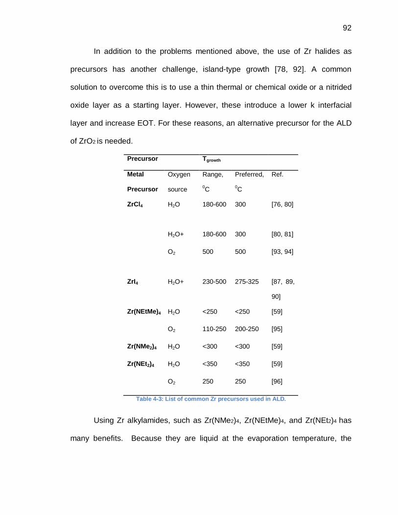
92
In addition to the problems mentioned above, the use of Zr halides as
precursors has another challenge, island-type growth [78, 92]. A common
solution to overcome this is to use a thin thermal or chemical oxide or a nitrided
oxide layer as a starting layer. However, these introduce a lower k interfacial
layer and increase EOT. For these reasons, an alternative precursor for the ALD
of ZrO2 is needed.
Precursor Tgrowth
Metal
Precursor
Oxygen
source
Range,
0C
Preferred,
0C
Ref.
ZrCl 4 H2O 180-600 300
[76, 80]
H2O+ 180-600 300 [80, 81]
O2 500
500 [93, 94]
ZrI4 H2O+ 230-500 275-325 [87, 89,
90]
Zr(NEtMe) 4 H2O <250 <250 [59]
O2 110-250 200-250 [95]
Zr(NMe2)4 H2O <300 <300 [59]
Zr(NEt 2)4 H2O <350 <350 [59]
O2 250 250 [96]
Table 4-3: List of common Zr precursors used in ALD .
Using Zr alkylamides, such as Zr(NMe2)4, Zr(NEtMe)4, and Zr(NEt2)4 has
many benefits. Because they are liquid at the evaporation temperature, the
93
particle contamination problem is eliminated [59]. The alkylamides are reactive
towards water and give reasonably low impurity levels [59]. However with Zr
alkylamides, higher carbon contents have been reported when oxygen or oxygen
plasmas were used as the oxygen source [95-98]. The main issue with the use of
alkylamides is their thermal stability. The decomposition of these precursors
limits the maximum growth temperature to 250°C. If smooth films are desired, the
growth temperature must be low [70].
The reported ALD processes for ZrO2 are listed in Table 4-3, where the
alternative processes, as expected, are very similar to the previously described
alternative HfO2 processes (Table 4-2).
Section 4.3 Oxygen Sources
In the ALD of metal oxide thin films, there are many different oxygen
sources including H2O, O2, O3, H2O2, oxygen plasmas, and metal alkoxides [4,
10]. Among them, water is the most common oxygen source. The order of the
oxidation power of these commonly used oxygen sources from high to low is
oxygen plasma > ozone > hydrogen peroxide > water.
In practice, the selection of oxygen precursor is more complicated.
Generally speaking, a strong oxidizer, like an oxygen plasma or ozone, can
produce denser films with lower impurity levels and enhanced electrical
properties [63, 99]. However, the strong oxidizer often causes the formation of a
fairly thick interfacial layer because it also oxidizes the substrate [99-101]. The

94
additional growth of low permittivity interfacial layers makes it difficult to achieve
low EOT values and excludes strong oxidizer processing as a good solution for
high-k gate dielectric fabrication.
On the other hand, oxidizers like water and H2O2 rely on hydroxyl groups on
the starting surface and high reactivity of the chemisorbed metal precursors.
Otherwise the initial nucleation during deposition may be inhibited resulting in
poor electrical properties of the films [78, 102].
In the metal-halide based process, replacing H2O with O3 decreases the Cl-
content in the bulk of the film and improved most of the dielectric properties,
including fixed charge, interface trap densities, and the leakage current
characteristics [63]. However, the higher oxygen content in the ozone-processed
films resulted in a thicker interfacial layer and thus increased EOT after rapid
thermal annealing (RTA) at 750 °C.
In the metal-alkylamide based process, ozone as the oxygen source
instead of water has gained considerable interest to grow HfO2 [55, 61, 101, 103,
104]. For example, using ozone instead of water with a Hf(NMe2)4 precursor at a
relatively high growth temperature of 300 °C reduce d the impurity contents and
the films showed a more amorphous structure leading to better leakage current
characteristics [105, 106]. However, in some studies the use of ozone did not
significantly reduce impurities nor enhance electrical properties as compared to
the use of water, but they did increase the thickness of the interfacial oxide layer
[55, 103].

95
Section 4.4 ALD System
In our work, ALD of high-k dielectrics were performed in a home-made ALD
system coupled to a commercial XPS system. Together with the metallization
chambers which have the ability to deposit various metals as the metal gate, this
integrated system makes in-situ study of advanced MOS devices possible.
Figure 4-8: The integrated XPS system with ALD and metallization chambers.
The ALD system consists of a sample introduction chamber, a reactor with
a sample heater and gas lines. A Ge wafer of 1” diameter or smaller is mounted
onto the sample holder which is compatible with the sample holder of the XPS
system and is then loaded into the system from the quick loadlock. The gate
valve between the reactor and the loadlock makes it possible to load a sample
without venting the reactor. The transfer rod is used to send the sample into the
reactor and mount it onto a sample heating platform where a thermocouple is

96
mounted to monitor the temperature of the sample. The whole system including
the sample is first preheated to 100-110 °C to deso rb water and then pumped
down to 10-6-10-7 Torr for an hour before the deposition starts. Several pneumatic
valves are installed to control the flow of gases and produce the alternative
pulses of precursors in ALD. The flow rate of purging N2 is set to 100 cc per
minute by a mass flow controller. A scroll pump is used to avoid the back
streaming of oil vapor from a mechanical pump. Together with an adjustable
throttle valve, the pressure of the reactor with N2 purging can be controlled to a
constant between 0.1-1.0 Torr. During deposition, the reactor and all gas lines
are heated with heating tapes and are maintained in a hot wall condition at fixed
elevated temperature in order to prevent the condensation of chemicals on the
chamber walls.

97
Figure 4-9: The schematic drawing of the ALD system .
The whole ALD system is monitored and controlled with a LabView
program running on a PC with a USB 12-bit DAQ board. With the Baratron
pressure gauge, and the thermocouples attached to the sample, the reactor, gas
lines and precursor bottles, the pressure and temperatures are logged at all
times. Using the LabView program, one can also easily configure temperature
set points for each part of the system and design customized ALD growth
parameters including gas pulse sequence, duration and number of cycles.

98
Section 4.5 Experimental Results of ALD Film Growth s
In this section, experimental results of ALD growth of Al2O3 and HfO2 on
various substrates are presented. With the help of RBS, the deposited film
thicknesses were determined as well as the growth rates per ALD cycle.
4.5.1 ALD of Al 2O3
In this work, Al2O3 films are deposited using the ALD system mentioned
above with TMA and water at 70-95 °C. In an RBS ran dom spectrum, since Si
and Ge are heavier than Al, the Al signal will usually be overwhelmed by the
substrate background signal. Figure 4-10 shows the random incident RBS
spectrum of Al2O3 films of the same thickness on Si and Ge substrates. On the
Ge substrate, the Al peak is buried in the Ge background and this makes it
difficult to precisely determine the thickness of Al2O3 films. In the case of
Al2O3/Si, the Al peak in the RBS spectrum is near the edge of Si background. As
long as the Al2O3 film is not too thin, one still can fit the spectra and extract the
film thickness. A simulation using SIMNRA gives the atomic areal density
1.70x10¹⁷ atoms/cm2 for the Al2O3 layer corresponding to a physical film
thickness of 156 Å. In this specific deposition, the number of ALD cycles is 200
and this gives a growth rate of about 0.78 Å/cycle.

99
Figure 4-10: RBS random scattering spectrum of Al 2O3 of the same thickness on Si (left) and Ge
(right).
A better way to determine the physical film thickness is to utilize RBS
channeling to suppress the background signal from the heavy substrate atoms.
In Figure 4-11, a channeling RBS spectrum of Al2O3 on ITO (indium tin oxide or
tin-doped indium oxide)/glass substrate is shown. Under the channeling
condition, the Si signal from glass has been suppressed and this increases
sensitivities of light elements like Al and O. Note that the O signal is not like a
single peak in the previous Al2O3/Si spectrum. This is because O signals are not
only from the Al2O3 layer on the top but also from ITO layer.
Since organic light emitting devices (OLEDs) [107] are extremely sensitive
to moisture and oxygen [108], a perimeter seal inside the device is required as a
protective barrier. UV-cured epoxy, the most commonly used method, is
inadequate for top-emitter OLEDs because the emitted light has to pass through

100
the cover glass and the opaque desiccant. PVD and CVD based methods have
been studied for the top-emitter encapsulation [109, 110]. Recently it has been
shown that ALD can be used to deposit a thin Al2O3 film as a dense, light-weight
and transparent encapsulating layer which can withstand accelerated testing at
85°C and high relative humidity (85%) for more than 1000 hours [111].
Figure 4-11: RBS spectra of Al 2O3 on ITO (left) and Kapton (right).
Al2O3 has been deposited on ITO and DuPont Kapton E polyimide films.
ITO is a mixture of indium oxide (In2O3) and tin oxide (SnO2). Because of its
electrical conductivity and optical transparency, ITO is commonly used in
LCD/LED/plasma displays, solar cells and OLEDs. DuPont Kapton E polyimide
film is a thermally stable dielectric film in a wide range of temperatures and this
also makes it a popular choice for the base plate of displays and OLEDs. In
Figure 4-12, it shows the growth rate is about 0.81 Å per ALD cycle.

101
Figure 4-12: Film thickness of Al 2O3 vs. number of ALD cycles.
4.5.2 ALD of HfO 2
HfO2 films were deposited on various type of substrates with Hf(NEtMe)4
and water in the 150-175 °C range. In Figure 4-13, a random incident RBS
spectrum of HfO2/GaAs is shown. Since Hf is heavy, the Hf peak is well
separated from the substrate signals of Ga and As. If determination of HfOx
composition is desired, a channeling RBS study can be done to suppress the
background and make the O peak more sensitive. In this spectrum, the
simulation with atomic areal density makes the best fit with the experimental data
and this suggests the physical film thickness is about 101 Å. There are 120 ALD
cycles and thus the growth rate is 0.84 Å/cycle. Repeating ALD of HfO2 with a
different number of cycles at the same growth temperature and the same cycle
settings gives a growth rate of about 0.83 Å/cycle shown in Figure 4-14.
y = 0.813xR² = 0.995
020406080
100120140160180200
0 50 100 150 200 250
Film Th
icknes
s (Å)
Number of ALD Cycles

102
Figure 4-13: Random scattering RBS spectrum of HfO 2/GaAs.
Figure 4-14: Film thickness of HfO 2 vs. number of ALD cycles.
ALD of HfO2 on clean Ge(100) and Si(100) were also performed. In Figure
4-15, random scattering RBS spectra show that 35 ALD cycles deposited 29.9 Å
of HfO2 on Ge (~0.85 Å/cycle) and 30 ALD cycles deposited 23.8 Å of HfO2 on
y = 0.834xR² = 0.991
0
50
100
150
200
250
0 50 100 150 200 250 300
Film Th
icknes
s (Å)
Number of ALD Cycles
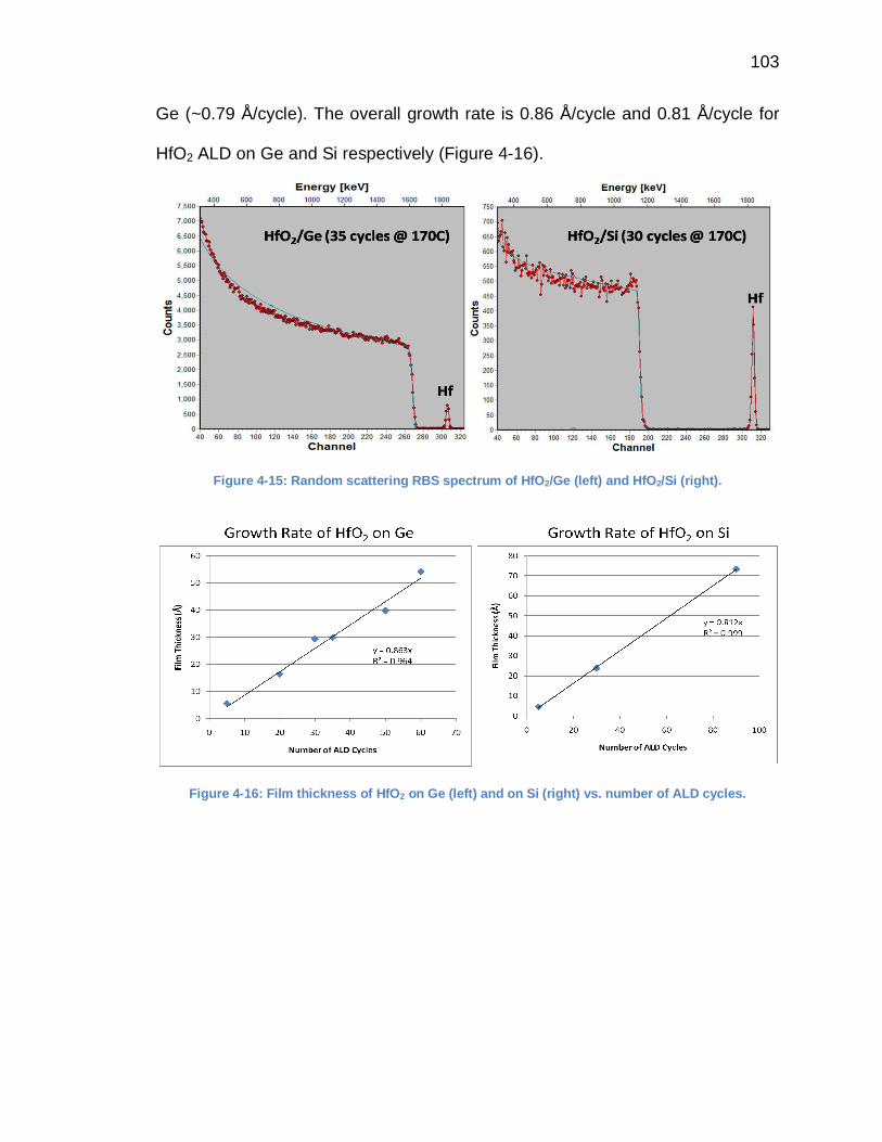
103
Ge (~0.79 Å/cycle). The overall growth rate is 0.86 Å/cycle and 0.81 Å/cycle for
HfO2 ALD on Ge and Si respectively (Figure 4-16).
Figure 4-15: Random scattering RBS spectrum of HfO 2/Ge (left) and HfO 2/Si (right).
Figure 4-16: Film thickness of HfO 2 on Ge (left) and on Si (right) vs. number of ALD c ycles.

104
Section 4.6 Reference
1. T. Suntola and J. Antson, A method for producing compound thin films. 1977: US Patent 4,058,430.
2. I.T.R.f. Semiconductors. Available from: http://www.itrs.net/. 3. A. Hand, Industry begins to embrace ALD. Semiconductor International, 2003. 26(5): p.
46-51. 4. M. Ritala and M. Leskelä, in Handbook of Thin Film Materials, H.S. Nalwa, Editor. 2002,
Academic Press: New York. p. 103-159. 5. L. Niinisto, M. Ritala, and M. Leskela, Synthesis of oxide thin films and overlayers by
atomic layer epitaxy for advanced applications. Materials Science and Engineering B-Solid State Materials for Advanced Technology, 1996. 41(1): p. 23-29.
6. M. Leskela and M. Ritala, Atomic layer deposition chemistry: Recent developments and future challenges. Angewandte Chemie-International Edition, 2003. 42(45): p. 5548-5554.
7. L. Niinisto, J. Paivasaari, J. Niinisto, et al., Advanced electronic and optoelectronic materials by Atomic Layer Deposition: An overview with special emphasis on recent progress in processing of high-k dielectrics and other oxide materials. Physica Status Solidi A-Applied Research, 2004. 201(7): p. 1443-1452.
8. M. Leskela and M. Ritala, Atomic layer deposition (ALD): from precursors to thin film structures. Thin Solid Films, 2002. 409(1): p. 138-146.
9. L. Niinisto, Atomic layer epitaxy. Current Opinion in Solid State and Materials Science, 1998. 3(2): p. 147-152.
10. R.L. Puurunen, Surface chemistry of atomic layer deposition: A case study for the trimethylaluminum/water process. Journal of Applied Physics, 2005. 97(12): p. -.
11. A. Delabie, R.L. Puurunen, B. Brijs, et al., Atomic layer deposition of hafnium oxide on germanium substrates. Journal of Applied Physics, 2005. 97(6): p. -.
12. J. Niinistö, Atomic layer deposition of high-k dielectrics from novel cyclopentadienyl-type precursors, in Department of Chemical Technology. 2006, Helsinki University of Technology: Espoo, Finland.
13. T. Suntola, Surface chemistry of materials deposition at atomic layer level. Applied Surface Science, 1996. 101: p. 391-398.
14. M. Ritala and M. Leskela, Atomic layer epitaxy - a valuable tool for nanotechnology? Nanotechnology, 1999. 10(1): p. 19-24.
15. T.S. Suntola, A.J. Pakkala, and S.G. Lindfors, Method for performing growth of compound thin films. 1983: U.S. Patent No. 4,413,022.
16. M. Pessa, R. Mäkelä, and T. Suntola, Characterization of surface exchange reactions used to grow compound films. Applied Physics Letters, 1981. 38(3): p. 131-132.
17. G.D. Wilk, R.M. Wallace, and J.M. Anthony, High-kappa gate dielectrics: Current status and materials properties considerations. Journal of Applied Physics, 2001. 89(10): p. 5243-5275.
18. R.M. Wallace and G.D. Wilk, High-kappa dielectric materials for microelectronics. Critical Reviews in Solid State and Materials Sciences, 2003. 28(4): p. 231-285.
19. M. Ylilammi, Monolayer thickness in atomic layer deposition. Thin Solid Films, 1996. 279(1-2): p. 124-130.

105
20. R.L. Puurunen, Growth per cycle in atomic layer deposition: A theoretical model. Chemical Vapor Deposition, 2003. 9(5): p. 249-257.
21. L. Hiltunen, H. Kattelus, M. Leskelä, et al., Growth and characterization of aluminium oxide thin films deposited from various source materials by atomic layer epitaxy and chemical vapor deposition processes. Materials Chemistry and Physics 1991. 28(4): p. 379-388.
22. M. Nieminen, L. Niinisto, and R. Lappalainen, Determination of P/Al Ratio in Phosphorus-Doped Aluminum-Oxide Thin-Films by Xrf, Rbs and Ftir. Mikrochimica Acta, 1995. 119(1-2): p. 13-22.
23. M. Ritala, H. Saloniemi, M. Leskela, et al., Studies on the morphology of Al2O3 thin films grown by atomic layer epitaxy. Thin Solid Films, 1996. 286(1-2): p. 54-58.
24. D. Riihela, M. Ritala, R. Matero, et al., Introducing atomic layer epitaxy for the deposition of optical thin films. Thin Solid Films, 1996. 289(1-2): p. 250-255.
25. S.J. Yun, K.H. Lee, J. Skarp, et al., Dependence of atomic layer-deposited Al2O3 films characteristics on growth temperature and Al precursors of Al(CH3)(3) and AlCl3. Journal of Vacuum Science and Technology A, 1997. 15(6): p. 2993-2997.
26. M. Nieminen and L. Niinisto, Determination of aluminium in AlCl3 and Al2O3 modified silica catalyst supports. Fresenius Journal of Analytical Chemistry, 1999. 364(3): p. 224-227.
27. K. Kukli, M. Ritala, and M. Leskela, Development of dielectric properties of niobium oxide, tantalum oxide, and aluminum oxide based nanolayered materials. Journal of the Electrochemical Society, 2001. 148(2): p. F35-F41.
28. M. Tiitta, E. Nykanen, P. Soininen, et al., Preparation and characterization of phosphorus-doped aluminum oxide thin films. Materials Research Bulletin, 1998. 33(9): p. 1315-1323.
29. K.E. Elers, M. Ritala, M. Leskela, et al., Nbcl(S) as a precursor in atomic layer epitaxy. Applied Surface Science, 1994. 82-3: p. 468-474.
30. J. Aarik, A. Aidla, K. Kukli, et al., Deposition and etching of tantalum oxide-films in atomic layer epitaxy process. Journal of Crystal Growth, 1994. 144(1-2): p. 116-119.
31. K. Kukli, J. Aarik, A. Aidla, et al., Atomic layer deposition of tantalum oxide thin films from iodide precursor. Chemistry of Materials, 2001. 13(1): p. 122-128.
32. H. Siimon and J. Aarik, Thickness profiles of thin films caused by secondary reactions in flow-type atomic layer deposition reactors. Journal of Physics D-Applied Physics, 1997. 30(12): p. 1725-1728.
33. M.A. Tischler and S.M. Bedair, Growth and characterization of compound semiconductors by atomic layer epitaxy. Journal of Crystal Growth, 1986. 77(1-3): p. 89-94.
34. J. Nishizawa, H. Abe, and T. Kurabayashi, Molecular layer epitaxy. Journal of the Electrochemical Society, 1985. 132(5): p. 1197.
35. G.S. Higashi and L.J. Rothberg, Surface photochemical phenomena in laser chemical vapor deposition Journal of Vacuum Science and Technology B, 1985. 3(5): p. 1460-1463.
36. M. Ozeki, K. Mochizuki, N. Ohtsuka, et al., Kinetic processes in atomic-layer epitaxy of GaAs and AlAs using a pulsed vapor-phase method Journal of Vacuum Science and Technology B, 1987. 5(4): p. 1184-1186.
37. S.M. Bedair, M.A. Tischler, T. Katsuyama, et al., Atomic layer epitaxy of III-V binary compounds. Applied Physics Letters 1985. 47(1): p. 51-53

106
38. A. Hunter and A.H. Kitai, A novel atmospheric pressure technique for the deposition of ZnS by atomic layer epitaxy using dimethylzinc. Journal of Crystal Growth, 1988. 91(1-2): p. 111-118.
39. A. Doi, Y. Aoyagi, and S. Namba, Stepwise monolayer growth of GaAs by switched laser metalorganic vapor phase epitaxy. Applied Physics Letters 1986. 49(13): p. 785-787
40. M. Putkonen, M. Nieminen, and L. Niinisto, Magnesium aluminate thin films by atomic layer deposition from organometallic precursors and water. Thin Solid Films, 2004. 466(1-2): p. 103-107.
41. R. Matero, A. Rahtu, M. Ritala, et al., Effect of water dose on the atomic layer deposition rate of oxide thin films. Thin Solid Films, 2000. 368(1): p. 1-7.
42. O. Sneh, R.B. Clark-Phelps, A.R. Londergan, et al., Thin film atomic layer deposition equipment for semiconductor processing. Thin Solid Films, 2002. 402(1-2): p. 248-261.
43. M.D. Groner, J.W. Elam, F.H. Fabreguette, et al., Electrical characterization of thin Al2O3 films grown by atomic layer deposition on silicon and various metal substrates. Thin Solid Films, 2002. 413(1-2): p. 186-197.
44. J.M. Jensen, A.B. Oelkers, R. Toivola, et al., X-ray reflectivity characterization of ZnO/Al2O3 multilayers prepared by atomic layer deposition. Chemistry of Materials, 2002. 14(5): p. 2276-2282.
45. R.L. Puurunen, W. Vandervorst, W.F.A. Besling, et al., Island growth in the atomic layer deposition of zirconium oxide and aluminum oxide on hydrogen-terminated silicon: Growth mode modeling and transmission electron microscopy. Journal of Applied Physics, 2004. 96(9): p. 4878-4889.
46. R.L. Puurunen, M. Lindblad, A. Root, et al., Successive reactions of gaseous trimethylaluminium and ammonia on porous alumina. Physical Chemistry Chemical Physics, 2001. 3(6): p. 1093-1102.
47. M. Ritala, M. Leskela, L. Niinisto, et al., Development of crystallinity and morphology in hafnium dioxide thin-films grown by atomic layer epitaxy. Thin Solid Films, 1994. 250(1-2): p. 72-80.
48. J. Aarik, A. Aidla, A.A. Kiisler, et al., Influence of substrate temperature on atomic layer growth and properties of HfO2 thin films. Thin Solid Films, 1999. 340(1-2): p. 110-116.
49. J. Aarik, A. Aidla, H. Mandar, et al., Texture development in nanocrystalline hafnium dioxide thin films grown by atomic layer deposition. Journal of Crystal Growth, 2000. 220(1-2): p. 105-113.
50. E.P. Gusev, C. Cabral, M. Copel, et al., Ultrathin HfO2 films grown on silicon by atomic layer deposition for advanced gate dielectrics applications. Microelectronic Engineering, 2003. 69(2-4): p. 145-151.
51. V. Kaushik, M. Claes, A. Delabie, et al., Observation and characterization of defects in HfO2 high-K gate dielectric layers. Microelectronics Reliability, 2005. 45(5-6): p. 798-801.
52. J.J. Ganem, I. Trimaille, I.C. Vickridge, et al., Study of thin hafnium oxides deposited by atomic layer deposition. Nuclear Instruments & Methods in Physics Research Section B-Beam Interactions with Materials and Atoms, 2004. 219-20: p. 856-861.
53. P.S. Lysaght, B. Foran, G. Bersuker, et al., Physicochemical properties of HfO2 in response to rapid thermal anneal. Applied Physics Letters, 2003. 82(8): p. 1266-1268.
107
54. M. Caymax, S. Van Elshocht, M. Houssa, et al., HfO2 as gate dielectric on Ge: Interfaces and deposition techniques. Materials Science and Engineering B-Solid State Materials for Advanced Technology, 2006. 135(3): p. 256-260.
55. D.H. Triyoso, R.I. Hegde, B.E. White, et al., Physical and electrical characteristics of atomic-layer-deposited hafnium dioxide formed using hafnium tetrachloride and tetrakis(ethylmethylaminohafnium). Journal of Applied Physics, 2005. 97(12): p. -.
56. J. Aarik, J. Sundqvist, A. Aidla, et al., Hafnium tetraiodide and oxygen as precursors for atomic layer deposition of hafnium oxide thin films. Thin Solid Films, 2002. 418(2): p. 69-72.
57. K. Kukli, M. Ritala, J. Sundqvist, et al., Properties of hafnium oxide films grown by atomic layer deposition from hafnium tetraiodide and oxygen. Journal of Applied Physics, 2002. 92(10): p. 5698-5703.
58. K. Kukli, M. Ritala, T. Sajavaara, et al., Comparison of hafnium oxide films grown by atomic layer deposition from iodide and chloride precursors. Thin Solid Films, 2002. 416(1-2): p. 72-79.
59. D.M. Hausmann, E. Kim, J. Becker, et al., Atomic layer deposition of hafnium and zirconium oxides using metal amide precursors. Chemistry of Materials, 2002. 14(10): p. 4350-4358.
60. K. Kukli, M. Ritala, J. Lu, et al., Properties of HfO2 thin films grown by ALD from hafnium tetrakis(ethylmethylamide) and water. Journal of the Electrochemical Society, 2004. 151(8): p. F189-F193.
61. S. Kamiyama, T. Miura, and Y. Nara, Electrical properties of ultrathin HfO2 films for replacement metal gate transistors, fabricated by atomic layer deposition using Hf(N(CH3)(C2H5))(4) and O-3. Applied Physics Letters, 2005. 87(13): p. -.
62. K. Kukli, M. Ritala, T. Sajavaara, et al., Atomic layer deposition of hafnium dioxide films from hafnium tetrakis(ethylmethylamide) and water. Chemical Vapor Deposition, 2002. 8(5): p. 199-204.
63. H.B. Park, M.J. Cho, J. Park, et al., Comparison of HfO2 films grown by atomic layer deposition using HfCl4 and H2O or O-3 as the oxidant. Journal of Applied Physics, 2003. 94(5): p. 3641-3647.
64. N. Takahashi, S. Nonobe, and T. Nakamura, Growth of HfO2 films using an alternate reaction of HfCl4 and O-2 under atmospheric pressure. Journal of Solid State Chemistry, 2004. 177(11): p. 3944-3948.
65. J.F. Conley, Y. Ono, D.J. Tweet, et al., Pulsed deposition of metal-oxide thin films using dual metal precursors. Applied Physics Letters, 2004. 84(3): p. 398-400.
66. S.I. Lee, J.S. Owyang, Y. Senzaki, et al., High-k gate dielectric applications using ALD Hf-based oxides. Solid State Technology, 2003. 46(1): p. 45.
67. K. Kukli, T. Pilvi, M. Ritala, et al., Atomic layer deposition of hafnium dioxide thin films from hafnium tetrakis(dimethylamide) and water. Thin Solid Films, 2005. 491(1-2): p. 328-338.
68. R.G. Gordon, J. Becker, D. Hausmann, et al., Vapor deposition of metal oxides and silicates: Possible gate insulators for future microelectronics. Chemistry of Materials, 2001. 13(8): p. 2463-2464.
69. S. Choi, J. Koo, H. Jeon, et al., Plasma-enhanced atomic-layer deposition of a HfO2 gate dielectric. Journal of the Korean Physical Society, 2004. 44(1): p. 35-38.
108
70. D.M. Hausmann and R.G. Gordon, Surface morphology and crystallinity control in the atomic layer deposition (ALD) of hafnium and zirconium oxide thin films. Journal of Crystal Growth, 2003. 249(1-2): p. 251-261.
71. M. Cho, H.B. Park, J. Park, et al., High-k properties of atomic-layer-deposited HfO2 films using a nitrogen-containing Hf[N(CH3)(2)](4) precursor and H2O oxidant. Applied Physics Letters, 2003. 83(26): p. 5503-5505.
72. A. Deshpande, R. Inman, G. Jursich, et al., Atomic layer deposition and characterization of hafnium oxide grown on silicon from tetrakis(diethylamino)hafnium and water vapor. Journal of Vacuum Science and Technology A, 2004. 22(5): p. 2035-2040.
73. J. Kim, S. Kim, H. Jeon, et al., Characteristics of HfO2 thin films grown by plasma atomic layer deposition. Applied Physics Letters, 2005. 87(5): p. -.
74. Y. Won, S. Park, J. Koo, et al., Initial reaction of hafnium oxide deposited by remote plasma atomic layer deposition method. Applied Physics Letters, 2005. 87(26): p. -.
75. J. Kim, S. Kim, H. Kang, et al., Composition, structure, and electrical characteristics of HfO2 gate dielectrics grown using the remote- and direct-plasma atomic layer deposition methods. Journal of Applied Physics, 2005. 98(9): p. -.
76. M. Ritala and M. Leskela, Zirconium dioxide thin-films deposited by ALE using zirconium tetrachloride as precursor. Applied Surface Science, 1994. 75: p. 333-340.
77. V. Sammelselg, E. Rauhala, K. Arstila, et al., Study of thin oxide films by electron, ion and synchrotron radiation beams. Mikrochimica Acta, 2002. 139(1-4): p. 165-169.
78. M. Copel, M. Gribelyuk, and E. Gusev, Structure and stability of ultrathin zirconium oxide layers on Si(001). Applied Physics Letters, 2000. 76(4): p. 436-438.
79. C.M. Perkins, B.B. Triplett, P.C. McIntyre, et al., Electrical and materials properties of ZrO2 gate dielectrics grown by atomic layer chemical vapor deposition. Applied Physics Letters, 2001. 78(16): p. 2357-2359.
80. K. Kukli, M. Ritala, J. Aarik, et al., Influence of growth temperature on properties of zirconium dioxide films grown by atomic layer deposition. Journal of Applied Physics, 2002. 92(4): p. 1833-1840.
81. J. Aarik, A. Aidla, H. Mandar, et al., Growth kinetics and structure formation of ZrO2 thin films in chloride-based atomic layer deposition process. Thin Solid Films, 2002. 408(1-2): p. 97-103.
82. H. Nohira, W. Tsai, W. Besling, et al., Characterization of ALCVD-Al2O3 and ZrO2 layer using X-ray photoelectron spectroscopy. Journal of Non-Crystalline Solids, 2002. 303(1): p. 83-87.
83. A. Rahtu and M. Ritala, Reaction mechanism studies on the zirconium chloride-water atomic layer deposition process. Journal of Materials Chemistry, 2002. 12(5): p. 1484-1489.
84. S. Ferrari, G. Scarel, C. Wiemer, et al., Chlorine mobility during annealing in N-2 in ZrO2 and HfO2 films grown by atomic layer deposition. Journal of Applied Physics, 2002. 92(12): p. 7675-7677.
85. C. Zhao, G. Roebben, H. Bender, et al., In situ crystallisation in ZrO2 thin films during high temperature X-ray diffraction. Microelectronics Reliability, 2001. 41(7): p. 995-998.
86. W.F.A. Besling, E. Young, T. Conard, et al., Characterisation of ALCVD Al2O3-ZrO2 nanolaminates, link between electrical and structural properties. Journal of Non-Crystalline Solids, 2002. 303(1): p. 123-133.

109
87. K. Kukli, K. Forsgren, M. Ritala, et al., Dielectric properties of zirconium oxide grown by atomic layer deposition from iodide precursor. Journal of the Electrochemical Society, 2001. 148(12): p. F227-F232.
88. K. Kukli, K. Forsgren, J. Aarik, et al., Atomic layer deposition of zirconium oxide from zirconium tetraiodide, water and hydrogen peroxide. Journal of Crystal Growth, 2001. 231(1-2): p. 262-272.
89. K. Kukli, M. Ritala, T. Uustare, et al., Influence of thickness and growth temperature on the properties of zirconium oxide films grown by atomic layer deposition on silicon. Thin Solid Films, 2002. 410(1-2): p. 53-60.
90. K. Forsgren, J. Westlinder, J. Lu, et al., Iodide-based atomic layer deposition of ZrO2: Aspects of phase stability and dielectric properties. Chemical Vapor Deposition, 2002. 8(3): p. 105-109.
91. K. Kukli, M. Ritala, M. Leskela, et al., Atomic layer deposition of HfO2 thin films and nanolayered HfO2-Al2O3-Nb2O5 dielectrics. Journal of Materials Science-Materials in Electronics, 2003. 14(5-7): p. 361-367.
92. T. Conard, W. Vandervorst, J. Petry, et al., TOF-SIMS as a rapid diagnostic tool to monitor the growth mode of thin (high k) films. Applied Surface Science, 2003. 203: p. 400-403.
93. N. Takahashi, N. Yoshii, S. Nonobe, et al., Self-limiting growth of ZrO2 films on a Si(100) substrate using ZrCl4 and O-2 under atmospheric pressure. Journal of Electronic Materials, 2003. 32(10): p. 1107-1110.
94. N. Yoshii, N. Takahashi, T. Nakamura, et al., Preparation of ZrO2 nano-films by an alternate reaction using ZrCl4 and O-2 under atmospheric pressure. Electrochemical and Solid State Letters, 2002. 5(9): p. C85-C86.
95. S.J. Yun, J.W. Lim, and J.H. Lee, PEALD of zirconium oxide using tetrakis(ethylmethylamino)zirconium and oxygen. Electrochemical and Solid State Letters, 2004. 7(12): p. F81-F84.
96. Y. Kim, J. Koo, J.W. Han, et al., Characteristics of ZrO2 gate dielectric deposited using Zr t-butoxide and Zr(NEt2)(4) precursors by plasma enhanced atomic layer deposition method. Journal of Applied Physics, 2002. 92(9): p. 5443-5447.
97. S.J. Yun, J.W. Lim, and J.H. Lee, Effect of plasma on characteristics of zirconium oxide films deposited by plasma-enhanced atomic layer deposition. Electrochemical and Solid State Letters, 2005. 8(11): p. F47-F50.
98. J.Y. Kim, S.H. Kim, H. Seo, et al., Deposition and plasma measurements of Zr-oxide films with low impurity concentrations by remote PEALD. Electrochemical and Solid State Letters, 2005. 8(3): p. G82-G84.
99. S.C. Ha, E. Choi, S.H. Kim, et al., Influence of oxidant source on the property of atomic layer deposited Al2O3 on hydrogen-terminated Si substrate. Thin Solid Films, 2005. 476(2): p. 252-257.
100. E.P. Gusev, E. Cartier, D.A. Buchanan, et al., Ultrathin high-K metal oxides on silicon: processing, characterization and integration issues. Microelectronic Engineering, 2001. 59(1-4): p. 341-349.
101. C.S. Park, N. Moumen, J.H. Sim, et al., Performance of HfO2/TiN gate stacks with in situ grown and O-3 chemical interfacial oxide layers. Applied Physics Letters, 2005. 87(25): p. -.

110
102. M.L. Green, A.J. Allen, X. Li, et al., Nucleation of atomic-layer-deposited HfO2 films, and evolution of their microstructure, studied by grazing incidence small angle x-ray scattering using synchrotron radiation. Applied Physics Letters, 2006. 88(3): p. -.
103. X.Y. Liu, S. Ramanathan, A. Longdergan, et al., AID of hafnium oxide thin film from tetrakis(ethylmethylamino)hafnium and ozone. Journal of the Electrochemical Society, 2005. 152(3): p. G213-G219.
104. Y. Senzaki, S. Park, H. Chatham, et al., Atomic layer deposition of hafnium oxide and hafnium silicate thin films using liquid precursors and ozone. Journal of Vacuum Science and Technology A, 2004. 22(4): p. 1175-1181.
105. M.J. Cho, D.S. Jeong, J. Park, et al., Comparison between atomic-layer-deposited HfO2 films using O-3 or H2O oxidant and Hf[N(CH3)(2)](4) precursor. Applied Physics Letters, 2004. 85(24): p. 5953-5955.
106. J. Park, M. Cho, S.K. Kim, et al., Influence of the oxygen concentration of atomic-layer-deposited HfO2 films on the dielectric property and interface trap density. Applied Physics Letters, 2005. 86(11): p. -.
107. S.A. VanSlyke, C.H. Chen, and C.W. Tang, Organic electroluminescent devices with improved stability. Applied Physics Letters, 1996. 69(15): p. 2160-2162.
108. J. McElvain, H. Antoniadis, M.R. Hueschen, et al., Formation and growth of black spots in organic light-emitting diodes. Journal of Applied Physics, 1996. 80(10): p. 6002-6007.
109. J.D. Affinito, M.E. Gross, C.A. Coronado, et al., A new method for fabricating transparent barrier layers. Thin Solid Films, 1996. 291: p. 63-67.
110. F. J. H. van Assche, R. T. Vangheluwe, J. W. C. Maes, et al., Digest of Technical Papers, 2004. XXXV: p. 696.
111. A.P. Ghosh, L.J. Gerenser, C.M. Jarman, et al., Thin-film encapsulation of organic light-emitting devices. Applied Physics Letters, 2005. 86(22): p. -.

111
Chapter 5 High-k/Ge MOS Capacitors
In this work, ALD of high-k dielectrics have been deposited on Ge with
various surface treatments including sulfur passivation as described above. The
interfacial properties are investigated using electrical characterization techniques.
A brief introduction to capacitance-voltage measurement methods will be
presented along with a few selected results from our work that demonstrate the
improvements of MOS devices due to our cleaning and passivation methods.
Section 5.1 C-V Measurements
Electrical characterization is an important part of gate stack research.
Because of the simplicity of operation and informative results, capacitance-
voltage measurements (CV) are one of the most popular methods to screen
potential dielectric and metal gate candidate materials [1]. This method is rather
straightforward and requires only a simple measurement.
5.1.1 Energy Band Diagrams of MOS Stacks and Flat-B and Voltage
C-V measurements require a capacitor, which is equivalent to the gate
stack part of a MOSFET. Figure 5-1 shows the band diagram of an ideal MOS
structure on a p-type semiconductor substrate. The work function of the metal +
is the energy required for an electron inside the metal to move from the Fermi
level to the vacuum level. The work function of the semiconductor, , is

112
determined by the electron affinity, _, the band gap, , and the Fermi potential `: _ 12 `
The Fermi potential depends on the ratio of the doping density, ?, and the
intrinsic carrier density, !: ` ln ?!
Assume that the two work functions are the same in this ideal MOS structure: + a + 0. The energy band diagram of the ideal MOS capacitor at
equilibrium is shown in Figure 5-1.
Figure 5-1: Energy band diagram of an ideal MOS cap acitor [1].
When an ideal MOS capacitor is biased, several different cases exist at
the semiconductor surface (Figure 5-3). Consider a p-type semiconductor; when
a negative voltage is applied to the metal gate, the band bending causes an
accumulation of majority p-type carriers and negative surface potential ` near

113
the semiconductor surface. This is the accumulation case. When a small positive
voltage is applied, the bands bend downward and the surface potential becomes
more positive. This is called the depletion case because the majority carriers are
depleted. Further increasing of the gate voltage in the positive direction causes
the bands to bend even more and the charge of the minority and majority carriers
at the surface switches. The surface becomes “inverted” with electrons
accumulating near the interface; this is the inversion case.
Theoretically, the potential, `,9X;, with respect to the bulk of the p-type
semiconductor, together with the space-charge density, 2, can be obtained by
solving the one-dimensional Poisson equation [1]: )`,9X;)X U9X;
At the surface of the semiconductor, ` is the surface potential (` a `,90;) and
it depends only on the properties of the semiconductors (band gap, dielectric
constant and doping level). Figure 5-2 shows a typical variation of the space-
charge density in a semiconductor as a function of the surface potential: 29`;
for a p-type Ge with ? 2.5 b 10 cm-3 at room temperature. Note that the
exponential term ~exp 9 ` 2 ⁄ ; dominates in both the accumulation and the
strong inversion cases, and the space-charge density, 2, for small positive
surface potential increases as ~8`. This is directly related to the voltage-
dependent semiconductor capacitance: )2)`

114
Figure 5-2: Space-charge density as a function of t he surface potential for p-type Ge with
NA=2.5x1022 cm -3 at room temperature.

115
Figure 5-3: Band diagrams for an ideal p-substrate MOS structure in different surface-charge
conditions (adapted from [1-3]).

116
When dealing with practical MOS systems, one needs to consider the
effects of real surfaces. First, there is a non-zero work function difference
resulting from the choice of the metal and the semiconductor as well as the
doping level of the semiconductor. Second, there are charges within the oxide
and at the oxide-semiconductor interface.
In the case of a non-zero, +, the band diagram at equilibrium has a tilt in
the oxide conduction band in order to align the Fermi levels shown in Figure 5-4a
and Figure 5-4b. As a result, the bands bend near the semiconductor surface to
accommodate the work function difference. In order to reach the flat-band
condition in which the surface potential, `, on the top of the semiconductor
vanishes, a bias is required on the gate (Figure 5-4c). This bias is the flat-band
voltage - +.
Figure 5-4: Band diagrams of MOS (a) at separation, (b) at equilibrium and (c) in flat-band condition
[3].

117
The equilibrium MOS structure is also affected by the existence of
charges in the insulator and at the interface between the oxide and
semiconductor (Figure 5-5). In earlier studies [1], the charges inside the oxide
layer were classified into (1) fixed oxide charges at or near the interface which
are immobile under an external electric field, (2) oxide trapped charges
distributed inside the oxide layer, and (3) mobile ionic charges such as sodium
ions. In the case of ultrathin oxide films, this classification needs to be revised
and currently there are still numerous studies on this issue. For simplicity, one
can include all of the charges inside the oxide in 2.
The interface trapped charge, 2, located in the high-k/semiconductor
interface, can be either positive or negative and are electrically active due to
interactions with the substrate. Studies have shown that the existence of the
interface charges, 2, within the forbidden gap results from the interruption of the
periodic lattice structure by impurities and defects in the interface [4-6]. With the
assumption that every interface has both acceptor and donor interface traps
within the forbidden-gap energies and the interface trapping levels are distributed
with an equivalent interface state density, f, with an neutral level, (the so-
called charge neutrality level, CNL) above which the states are of acceptor type
and below which are of donor type, then the interface trapped charges can be
calculated by 2 P f
) P f
)

118
Even on a clean surface in an UHV system, 2 can be very high. Proper surface
passivation and post deposition annealing can help reduce 2.
The effective trapped charge, 2, is then defined as the sum of various
oxide and interface charges (2 2 2 ) and it shifts the flat-band voltage: - + 2
where is the oxide capacitance. The next section will explain how to obtain - experimentally from a C-V measurement.
Figure 5-5: (a) Charges represented as a sheet of e ffective charge [2]; (b) interface traps [7].
5.1.2 C-V Curves of MOS Capacitors and Threshold Vo ltage
When the gate voltage is varied, the MOS capacitance varies due to the
accumulation, depletion and inversion of charge carriers in the semiconductor
substrate near the dielectric interface. The equivalent capacitance of a MOS
capacitor can be regarded as a combination of a fixed, voltage-independent

119
oxide capacitance and a contribution from the semiconductor substrate. In a
practical MOS system, trapped charges also contribute to this voltage-dependent
capacitance in the inversion region. The equivalent circuits are shown in Figure
5-6 to illustrate this idea.
Figure 5-6: Equivalent circuits including interface -trapped effects (a), at high (b) and low frequency
(c).
In the accumulation case, the semiconductor capacitance, , is very high
because the slope of the space-charge density, 2, versus ` plot is very steep
as shown in Figure 5-2. Hence, the series capacitance in the accumulation case
is just the oxide capacitance, (Figure 5-6a). The capacitance extreme, , in
the accumulation case from a C-V measurement can be used to calculate the
dielectric constant of the oxide if the physical thickness ) of the oxide is obtained
by another method like RBS: )

120
As the gate voltage becomes less negative, the semiconductor surface is
depleted. The depletion-layer capacitance, , is added in series with (Figure
5-6b): 1 1 1
where is the depletion width in the semiconductor substrate and is given by 2J`?
In the depletion region, the MOS capacitance decreases as 1 8`⁄ , while the
depletion width grows with increasing gate voltage across the capacitor. When
the flat-band condition is reached, the MOS capacitance, -, is given by: 1- 1 1)./)
where )./) is the Debye length capacitance of the substrate and is determined
by the extrinsic Debye length, : )./)
J?
While the gate voltage becomes more positive than the flat-band voltage,
the MOS capacitance keeps decreasing until strong inversion is reached at the

121
threshold voltage, 0. At this point, the surface potential is twice the Fermi
potential: `9g!h; 2`
Figure 5-7: Band diagram and distribution of charge density in inversion [1, 3].
Figure 5-7 shows the details of the energy bands and the distribution of
charges. The inversion charge 21 is negligible compared to the depletion
charge, 2, in the inversion case, so the total surface charge, 2, is mostly due to
the depletion charge: 2 21 2 Q 2 ?
The threshold voltage, 0, required for strong inversion, using the above
equations, is then given by:

122
0 - `9g!h; 2 Q - 2` 2
Figure 5-8: C-V curve for an ideal p-substrate MOS capacitor at high (HF) and low (LF) frequency [7].
Further increases in the voltage beyond the threshold voltage, 0, result in
strong inversion with a maximum depletion width, . The small signal
capacitance now depends on the frequency at which the measurement is made.
In a high-frequency measurement, a small-signal measuring voltage at high
frequency (100 kHz in this work) is applied. The gate voltage varies faster than
the generation-recombination rate of the minority carriers in the inversion layer.
The charge in the inversion layer cannot change in response, so it does not
contribute to the capacitance. Hence the MOS capacitance remains at its
minimum, +1, corresponding to the minimum depletion-layer capacitance, +1, resulting from the maximum depletion width (Figure 5-7): 1+1 1 1 +1

123
This capacitive behavior is shown as the high frequency “HF” curve in Figure 5-8. +1 extracted from a high-frequency C-V measurement can be used to
determine the value of the depletion width maximum, +, the substrate doping, ?, the Debye length capacitance, , flat-band capacitance, -, and the flat-
band voltage, - .
If the C-V measurements are done at low frequency, the MOS
capacitance in the strong inversion case at low-frequency will become very
different from that obtained by high-frequency measurements. Because the gate
voltage changes slowly at low frequency, there is enough time for minority
carriers to be generated in the bulk, drift across the depletion region to the
inversion layer, or go back to the substrate and recombine. The charge in the
inversion layer also contributes to the capacitance. In an ideal MOS capacitor,
this is the space charge, 2, induced by the electric field. Now the semiconductor
capacitance )2 )`⁄ is very large in the strong inversion case because the
space-charge density grows exponentially (Figure 5-2). Again the MOS series
capacitance at low frequency is . The low frequency “LF” curve in Figure 5-8
shows in the strong inversion region. In a practical MOS system, the interface
charge also contributes to the capacitance in the strong inversion case. The
equivalent circuit is shown in Figure 5-6c.
The deep-depletion region is shown as the “DD” curve in Figure 5-8. This
corresponds to the experimental situation in which both the gate voltage and the
small-signal measuring voltage vary too rapidly to form an inversion layer in the

124
surface depletion region. As a result, the depletion layer becomes wider than
and there is no capacitance minimum in deep depletion.
Section 5.2 Effects of Trapped Charges on C-V Curve s
One goal of this work is to minimize the trapped charges using the sulfur
passivation of Ge before the deposition of high-k dielectrics. As mentioned in the
previous section, there are two sources of the trapped charges: the trapped
charges in the oxide layer and the interface traps.
5.2.1 Shifts of Flat-Band Voltage and Hysteresis of C-V Curves
In an ideal MOS capacitor without trapped charges, the flat-band voltage
is given by the work function difference of the metal and the semiconductor, +,
which shifts the flat-band voltage without distortion (the dashed line in Figure
5-9).

125
Figure 5-9: C-V curve with nonzero work function di fference (dashed) and trapped charges (dotted)
[7].
However, the C-V curve is shifted as well as distorted in the presence of the
trapped charges (the dotted line in Figure 5-9). The flat-band voltage can be
extracted from the C-V curve and compared to an ideal C-V curve. This shift is
directly related to the amount of the effective trapped charge, 2, by: Δ- 2
In practical MOS systems, C-V measurements might exhibit hysteresis
effects as shown in Figure 5-10. These measurements are made when the gate
voltage is swept back and forth with a very low frequency of a triangular wave
(~1Hz) and a high-frequency ac measurement (1kHz or higher). The hysteresis
can help differentiate between two common non-ideal behavior patterns: (1) the
field-aided movement of the positive ions in the oxide layer, and (2) the trapping
of free carriers from the channel in traps at the oxide/semiconductor interface 2.
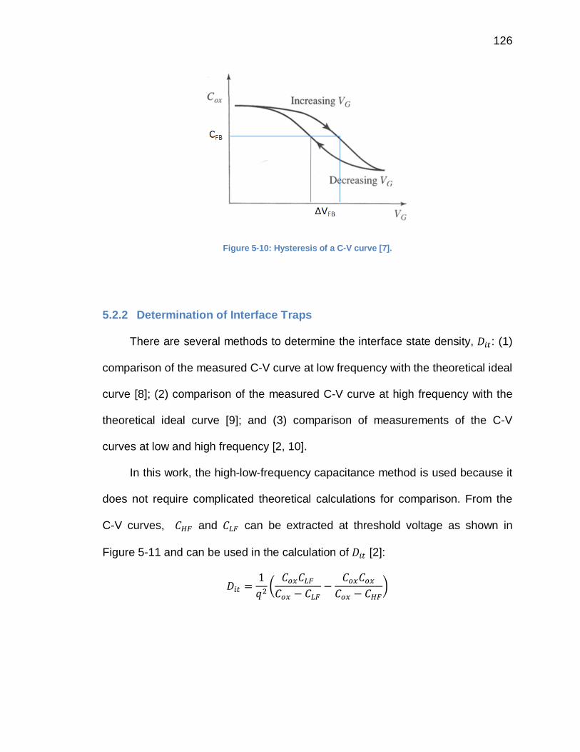
126
Figure 5-10: Hysteresis of a C-V curve [7].
5.2.2 Determination of Interface Traps
There are several methods to determine the interface state density, f: (1)
comparison of the measured C-V curve at low frequency with the theoretical ideal
curve [8]; (2) comparison of the measured C-V curve at high frequency with the
theoretical ideal curve [9]; and (3) comparison of measurements of the C-V
curves at low and high frequency [2, 10].
In this work, the high-low-frequency capacitance method is used because it
does not require complicated theoretical calculations for comparison. From the
C-V curves, - and - can be extracted at threshold voltage as shown in
Figure 5-11 and can be used in the calculation of f [2]: f 1 1 - - -3

127
Figure 5-11: C-V curves at high (solid line) and lo w (dotted line) frequencies [7].
Section 5.3 Experimental Results
The Ge-based MOS capacitors studied in this work were fabricated on p-
type Ge(100) wafers with ? 2.5 b 10 cm-3. The Ge surface pretreatments
included degreasing, wet chemical cleaning (HF etches and/or H2SO4/H2O2
oxidation) and optional passivation with sulfur using (NH4)2S solution as shown in
Section 5.3. A thin layer of HfO2 was deposited in our home-made ALD system
with Hf(NEtMe)4 and DIW as precursors. The film growth conditions are given in
Section 4.5. The physical film thickness of the HfO2 layer has been determined
by RBS to be 4.0 nm after 50 ALD cycles. An array of 200 nm-thick Au dots (100
µm in diameter) as metal gates were e-beam sputtered onto the high-k layer. All
samples were annealed at 500 °C for 30 seconds befo re the C-V measurements.
The sweeping dc bias is applied on the gate from -2 to 2 volts with a small ac
signal (20 mV) at high and low frequencies (1M and 100k Hz). Figure 5-12 shows

128
the stack structures of the Ge-based MOS capacitors and the setup of the C-V
measurement.
Figure 5-12: Schematic drawing of the C-V measureme nt setup.
5.3.1 HfO2/Ge
C-V measurements have been performed on Au/HfO2/p-Ge(100) MOS
capacitors with different surface treatments on the Ge substrates. Figure 5-13
shows the C-V curves of such a sample with an HF-last Ge substrate. Comparing
the measurements with the calculated ideal C-V curve, the effective trapped
charge, 2, can be obtained as shown in Section 5.2.1 and has a value of 4 b 10 e-1cm-2. After the flat-band capacitance, -, is determined, the amount
of the offset of the corresponding voltages, ∆-_, from the dual sweep C-V
curve (Figure 5-10) can be used as a quantitative measure of how big the
hysteresis is. For this sample, it is 0.31 V. The value of the interface state
density, f, has been extracted using the method in Section 5.2.2 and has a

129
value of 3.80 b 10 cm-2/eV. With such a large effective charge and big C-V
hysteresis, this MOS capacitor is unacceptable, in this condition, due to its
electrical performance.
Figure 5-13: C-V curves of a Au dot capacitor with 4 nm HfO 2 on HF-last p-Ge(100).
We now compare the electrical characteristics of Au/HfO2/p-Ge(100) MOS
capacitors fabricated with and without the sulfur passivation. Figure 5-14 shows
the C-V curves of a Au/HfO2/p-Ge(100) MOS capacitor on a sulfur-passivated Ge
substrate. Comparing with Figure 5-13, the C-V hysteresis is smaller (∆-_ 0.29 V) and the C-V curve is less distorted. This implies that the amount of the
effective trapped charge is smaller (2 4.17 b 10 e-1cm-2). The value of the
interface state density, f, is 1.67 b 10 cm-2/eV. This great reduction on f is
due to the sulfur passivation which terminates the dangling bonds on Ge
surfaces [11].
00.10.20.30.40.50.60.7
-3 -2 -1 0 1 2 3
Capaci
tance (
µF/cm
2 )
Gate Voltage (V)
1MHz100kHz

130
Figure 5-14: C-V curves of a Au dot capacitor with 4 nm HfO 2 on HF/DIW/H2O2-treated S-passivated p-
Ge(100).
Figure 5-15 shows the C-V curves of a Au/HfO2/p-Ge(100) MOS capacitor
on a sulfur-passivated Ge substrate. The degreased Ge substrate was first
cleaned using the H2SO4/H2O2 oxidation method. Before being passivated in
(NH4)2S solution, the substrate was etched by HF to remove the chemical oxide
formed in the previous step. Both the C-V hysteresis and the amount of the
effective trapped charge are further reduced (∆-_ 0.22 V and 2 3.56 b10 e-1cm-2). Comparing this to the C-V curves from the previous two samples in
Figure 5-13 and Figure 5-14, the shoulder due to the distortion becomes less
noticeable. The value of the interface state density, f, is 8.91 b 10 cm-2/eV.
0
0.2
0.4
0.6
0.8
1
1.2
-3 -2 -1 0 1 2 3
Capaci
tance (
µF/cm
2 )
Gate Voltage (V)
1MHz100kHz

131
Figure 5-15: C-V curves of a Au dot capacitor with 4 nm HfO 2 on H2SO4/H2O2 oxidized, HF-etched S-
passivated p-Ge(100).
In Section 3.1, we have shown that using HF should be avoided in order to
minimize the amount of hydrocarbons after the protective chemical oxide is
formed on the Ge surface. Figure 5-16 shows the C-V curves of another
Au/HfO2/p-Ge(100) MOS capacitor. It is similar to the previous one, except that
the HF etching step is omitted during the surface preparation (degreasing,
H2SO4/H2O2 oxidation and sulfur passivation). Among these four samples, it has
the smallest C-V hysteresis, the least amount of effective trapped charge
(∆-_ 0.15 V and 2 3.19 b 10 e-1cm-2) and the lowest value of interface
state density f (6.23 b 10 cm-2/eV).
The values of 2, ∆-_ and f obtained from these samples are listed
in Table 5-1 for easy comparison.
0
0.2
0.4
0.6
0.8
1
1.2
-3 -2 -1 0 1 2 3
Capaci
tance (
µF/cm
2 )
Gate Voltage (V)
1MHz100kHz

132
Figure 5-16: C-V curves of a Au dot capacitor with 4 nm HfO 2 on H2SO4/H2O2 oxidized, S-passivated
p-Ge(100).
Table 5-1: Comparison of the C-V measurements on Au /HfO2/p-Ge(100) capacitors.
0
0.2
0.4
0.6
0.8
1
1.2
-3 -2 -1 0 1 2 3
Capaci
tance (
µF/cm
2 )
Gate Voltage (V)
1MHz100kHz

133
Our results are significantly better than those reported in the literatures to
date. Figure 5-17 shows the C-V curves from a Al dot capacitor with 7.7 nm HfO2
on sulfur passivated n-Ge(100) from a recent study [12]. The minimum, extracted
from their C-V measurement, is 2.4 b 10 cm-2/eV which is about 40 times larger
than our best results (Table 5-1).
Figure 5-17: C-V curves of Al dot capacitors with 7 .7 nm HfO 2 on S-passivated n-Ge(100) [12].
5.3.2 Al 2O3/Ge
The improvement of the electrical properties due to the sulfur passivation
was also observed on Ge-based MOS capacitors with Al2O3 as a dielectric. For
comparison, ALD-grown Al2O3 was deposited on p-Ge(100) with and without a
sulfur passivated layer. Figure 5-18 shows the C-V curves obtained from such
two Au/Al2O3/p-Ge(100) capacitors. The capacitor with the sulfur passivation has
smaller C-V hysteresis and lower f than the one without the sulfur passivation.

134
Figure 5-18: C-V curves of Au/Al 2O3/p-Ge(100) with (right) and without (left) the sulf ur passivation.
In summary, the C-V measurements show that the Ge-based MOS
capacitors with the sulfur passivation exhibit lower f and smaller flat-band
voltage shifts than the ones without the sulfur passivation. This indicates that
sulfur passivation can efficiently reduce the trapped charge density and improve
electrical properties. The same trend has been observed on capacitors with HfO2
as well as Al2O3 as the high-k dielectric. Moreover, different wet chemical
pretreatments of the Ge substrates affect the C-V characteristics differently.
From our studies, the MOS capacitor on S-passivated Ge substrates which were
cleaned with H2SO4/H2O2 oxidation without following HF etches gives the best
electrical measurement results.
0
0.2
0.4
0.6
0.8
-3 -2 -1 0 1 2 3
Capaci
tance (
µF/cm
2 )
Gate Voltage (V)
0
0.2
0.4
0.6
0.8
-3 -2 -1 0 1 2 3
Capaci
tance (
µF/cm
2 )
Gate Voltage (V)

135
Section 5.4 Reference
1. S.M. Sze, Physics of Semiconductor Devices. 2nd ed. 1981, New York: Wiley. 2. B.G. Streetman and S.K. Banerjee, Solid State Electronic Devices. 6th ed. 2005: Prentice
Hall. 3. R. Pierret, Semiconductor Device Fundamentals. 2003: Pearson Higher Education. 4. I. Tamm, Phys. Z. Sowjetunion, 1933. 1: p. 733. 5. W. Shockley, On the surfaces states associated with a periodic potential. Physics Review,
1939. 56: p. 317. 6. E.H. Nicollian and J.R. Brews, MOS Physics and Technology. 1982, New York: Wiley. 7. R.S. Muller, T.I. Kamins, and M. Chan, Device Electronics for Integrated Circuits. 3rd ed.
2002: John Wiley & Sons. 8. L.M. Terman, An investigation of surface states at a silicon/silicon dioxide interface
employing metal-oxide-silicon diodes. Solid-State Electron, 1962. 5: p. 285. 9. C.N. Berglund, Surface state at steam-grown silicon-silicon dioxide interface. IEEE
Transactions on Electron Devices, 1966. ED-13: p. 701. 10. R. Castagne and A. Vapaolle, Description of the SiO2-Si interface properties by means of
very low frequency MOS capacitance measurements. Surface Science, 1971. 28: p. 157. 11. T. Maeda, S. Takagi, T. Ohnishi, et al., Sulfur passivation of Ge (001) surfaces and its
effects on Schottky barrier contact. Materials Science in Semiconductor Processing, 2006. 9(4-5): p. 706-710.
12. M.M. Frank, S.J. Koester, M. Copel, et al., Hafnium oxide gate dielectrics on sulfur-passivated germanium. Applied Physics Letters, 2006. 89(11): p. -.

136
Chapter 6 Conclusion
Scaling CMOS devices is key to the development of semiconductor
technology. However, further reduction in the thickness of the traditional SiO2
dielectric, now ~1 nm, would result in a dramatic increase in the leakage current
and hence degrade the device performance and increasing power consumption
well beyond what is acceptable. High-k dielectric materials like HfO2 and Al2O3
have been examined as replacements to SiO2 and are beginning to appear in
commercial devices just as this thesis work is finished. With SiO2 on the way out,
the need for Si also becomes a hindrance, and other higher performance
semiconductor are being suggested, with Ge showing some advantages such as
higher mobility relative to Si.
Because of the low thermal and chemical stability of Ge oxides, surface
cleaning and preparation on germanium is not as straightforward as it is for Si. In
this work, different wet-chemical cleaning methods on Ge substrates have been
studied. Unfortunately, none of them appear to fully remove all the hydrocarbon
and germanium carbides from the surface. By chemical oxidation, we can
convert these into other chemical species, which are more easily removed. This
approach seems to be a very promising solution. We have demonstrated that
H2SO4/H2O2 oxidation not only can greatly reduce the amount of the
hydrocarbons and germanium carbides, but it can also form a protective oxide to
prevent the surface from further contamination in ambient conditions. After the
137
chemical oxide is formed, we also found that HF etches should be avoided in
order to reduce the amount of carbon remaining or adsorbing on the surface.
Surface passivation is another crucial step for the success of the Ge-based
MOS devices. In this work, two different passivation chemistries (with hydrogen
and sulfur) have been studied and compared. S-passivated Ge surfaces
prepared in hot (NH4)2S solution are more stable than H-terminated Ge surfaces.
We have demonstrated that the combination of H2SO4/H2O2 oxidation and the
sulfur passivation with (NH4)2S have produced a clean Ge surface with the least
amount of carbons and Ge oxides.
Atomic layer deposition proves to be a very useful technique for the growth of
ultra-thin high-k films. In our home-built ALD system, ALD-grown HfO2 and Al2O3
have been deposited on Ge as well as other substrates including Si and glass.
The physical thickness and the growth rate have been determined by RBS.
Combining our work of the wet-chemical cleaning, the surface passivation
and ALD of high-k films, we are able to optimize the fabrication of novel Au/high-
k/Ge-based MOS capacitors. The interfacial properties have been investigated
using the electrical characterization techniques, including capacitance-voltage
measurements. The trap state density and the effective trapped charge have
been extracted from the results of the C-V measurements and have been used to
compare the effects of different surface preparation on Ge substrates. A great
improvement of MOS devices due to the sulfur passivation has been observed.
The future work should be focus on the further reduction of trapped charges and

138
interface state density and improvement of high-k film quality in order to minimize
leakage current and increase the MOS capacitance.
139
Curriculum Vista
Chien-Lan Hsueh
1997 B.S. in physics, National Tsing Hua University, Taiwan 1997-1998 Research assistant, National Synchrotron Radiation Research
Center, Taiwan 2000 M.S. in physics, National Taiwan University, Taiwan 2008 Ph.D., Department of Physics and Astronomy, Rutgers, The State
University of New Jersey. Publications: 1. X.G. He, C.-L. Hsueh and J.Q. Shi, “Constraints on the phase gamma and
new physics from B -> K pi decays”, Physical Review Letters 84 (1): 18-21 JAN 3 2000
2. J.B. Neaton, C.-L. Hsueh, and K.M. Rabe 2002, ”Enhanced polarization in strained BaTiO3 from first principles”, Materials Research Society (MRS) Proceedings 718: D10.26
3. M.M. Frank, H. Shang, S. Rivillon, F. Amy, C.-L. Hsueh, V. Paruchuri, R.T. Mo, M. Copel, E.P. Gusev, M.A. Gribelyuk, Y.J. Chabal, “High-kappa gate dielectrics on silicon and germanium: Impact of surface preparation”, Solid State Phenomena 103-104: 3-6 2005
4. E. Garfunkel, L. Goncharova, S. Rangan, C.-L. Hsueh, O. Celik, R. Bartynski
and T. Gustafsson, “Interface Characaterization in Nanoelectronics", The E4 Symposium "High Dielectric Constant Materials and Gate Stack 5," of the 212th Meeting of the Electrochemical Society. Washington, DC. 2007