ali alshehab tyler christensen dec. 11, 2013 -...
TRANSCRIPT

Ali AlShehab
Tyler Christensen
Dec. 11, 2013
6.111 Final Proposal
The Hard Core Digital Oscilloscope
Project Overview
Our final project uses the lab FPGA to implement a digital oscilloscope. An analog signal
is sampled through an analog-to-digital converter (ADC), and the FPGA lab kit reads, analyzes,
and visualizes the data on a VGA display output by showing the collected waveform as well as
some information about it in alpha numeric characters, such as min, max, and mean voltage. The
project has 7 input buttons used to set the levels of the voltage scaling, time scaling, and trigger
level (as well as trigger reset). These parameters work exactly as they do on a typical retail
oscilloscope.
Figure 1 – System Architecture – A simplified block diagram showing the data flow from the input stage to
the display stage. The two sections are separated by a dashed red line, with Tyler’s component being the
upper left and Ali’s being the lower right. The data is sampled by an external ADC chip, fed to data
acquisition for storage, processed, and finally displayed on a video output
The project is divided into two main components, the input stage (completed by Tyler)
and the display stage (completed by Ali). The separation of these two halves of the project can be
seen in figure 1. A block diagram showing the layout of the logic can be seen in figure 1 above.
The ADC, triggering, sampling, computation, plotting, and scaling modules are components of

the input stage and culminate in a BRAM containing data to be plotted on the screen. The
character map, rendering, and VGA modules are in the display stage and are responsible for
taking the plot data and waveform text and displaying them on the screen.
Input Stage (Written by Tyler):
This half of the project is responsible for taking the analog input signal and processing it
until it is ready to be displayed. This begins by putting the analog input voltage signal into a 12-
bit 10MSPS ADC to convert it into a digital signal. This digital signal is then analyzed by a
triggering module which finds an appropriate location in the wave to trigger the sampling
module to start collecting data. After 768 samples (the width of the waveform in pixels), the
computation module scales the voltages so that they correspond to the user-selected
voltage/division setting. The computation module also extracts the minimum, maximum, and
average voltages, and the signal frequency. The waveform and these extracted parameters are
passed to the display portion of the project to be shown on the VGA output screen.
I. ADC
The ADC hardware consists of a 20 MSPS 12-bit parallel ADC chip (Texas Instruments
ADC12020) which will be clocked at 10.125MHz from the FPGA labkit. A complete schematic
of the input stage can be seen below in figure 2.
Figure 2 - Schematic of the ADC input showing the offset and gain amplifier followed by the ADC chip. The
ADC chip's clock and output signals interface directly to the labkit FPGA.
The input voltage into the ADC chip must be centered about VREF which is set by R1, R2,
and R3. In the configuration selected here, the ADC has VREF at 1v and therefore VIN+ should be
1v for zero input signal into the scope. To accomplish this, the emitter of Q1 is biased at -1v. The
feedback path around IC1 causes the output of the op-amp to be centered at 1v, the mirror of the
bias voltage at the emitter of Q1. The feedback path also gives the output from the op-amp a gain
of two. This offset and gain-of-two signal is fed into the ADC chip.
The ADC requires a clock signal to operate, and runs in free-running mode as long as the
clock is present; that is, no sample-request signal is necessary which makes this chip perfect for
this application since the FPGA should always leave the ADC chip sampling at the maximum
rate. The clock to the ADC is 10.125MHz, and is derived from the 27MHz system clock through
a 15/40 multiplier.
The combination of R8 and C14 provide a 3db frequency cutoff of 1.6MHz to avoid
aliasing of high frequency input signals above half the sampling rate of the ADC chip.
II. Triggering
The triggering module must analyze the input waveform to determine appropriate times
to trigger the sampler to begin sampling. The importance of the trigger is to make sure the times
selected to begin sampling are always at the same position in the periodic waveform. If this were
not accomplished, the waveform would jitter around the screen with every re-draw, and would be
impossible to visually analyze. The solution implemented in this project is to use a comparator
between the input signal and a user programmable trigger level, as seen in figure 3. When a
specific edge (could be selected as rising or falling) occurs in the trigger signal, a trigger
command is sent to the sampling module. If the sampling module is not already sampling, it
begins a new sampling cycle. A sampling cycle describes the process of sampling 768 samples to
fill the plot screen. If it is already in the middle of a sampling cycle, it ignores the trigger signal
and continues sampling until 768 samples are taken.

Figure 3 - Triggering system: The input signal is compared wtih a user programmable trigger level. When the
signal is greater than the trigger level, the trigger signal is high. Otherwise, the trigger signal is low. A trigger
event occurs on one of the edges of the trigger signal.
Unfortunately implementing a simple software comparator is only sufficient in theory. In
practical application, a noise spike could create a trigger event. The first test was done with a simple
comparator, and the sampler was very frequently triggered on noise which created a jittery signal. The
solution to this is to make the comparator a state machine which requires the waveform to cross the
trigger level for a fixed number of ADC cycles before the trigger signal is switched. When this is
required, a noise spike does not meet the requirement for switching the trigger signal. This can be
accomplished using the following code:
module comparator #(parameter WIDTH=12) (input [WIDTH-1:0] a,
input [WIDTH-1:0] b, output reg out, input clock, input sysclock);
//The comparator requires a compare change event to occur for
//more than latchMax sequential cycles or the event is discarded
//as noise
parameter [3:0] latchMax = 4'd8;
reg [3:0] latch;
initial begin
latch=0;
end
always @(posedge clock) begin
//Watch for a change when latch=0, the reset state
if (latch==4'd0 && out!=(b>a)) begin
//Set latch to latchMax since a possible compare event occurred
latch<=latchMax;
end
if (latch!=4'd0) begin
if (out!=(b>a)) begin
latch<=latch-1;
if (latch==4'd1) out<=(b>a);
end else latch<=4'd0; //Reset latch system since compare-match is
no longer true
end
end
endmodule
When a potential trigger event is detected, latch is set to latchMax which begins the state
machine to count latch back down to zero. If at any point the trigger event condition is no longer
met, then it is assumed to be noise in the input signal and latch is again set to zero and a new
potential trigger event is waited for. Should it be a legitimate trigger event in the input signal,
latch will count down to zero and the trigger output will shift, signaling a trigger event.
III. Debounce and Scaling
The debounce module simply takes button inputs and debounces them using the 6.111-
provided debounce module. These signals are passed to the scaling module, which takes the user
input buttons and determines the user selected volts per division and time per division settings
for the scope. These settings are of fixed value, and the scaling module acts as a state machine
with each setting acting as a state and being user adjustable. The settings are discussed further in
their respective section below. This module also handles the input buttons which allow the user
to adjust the trigger level between -4 and +4 volts.
IV. Capture
When the trigger event is detected as described previously, the capture module is signaled
to begin a capturing cycle. This module also takes an input from a user-controllable time per
division setting, which operates exactly as the time per division knob on a typical oscilloscope.
There are a variety of settings ranging from 6us/div to 3ms/div with pre-programmed values
which are frequencies obtainable by dividing 10.125MHz. When the time scale setting is
anything slower than the maximum 6us/div (64 pixels/10,125,000), only every nth
sample is

stored and the rest are discarded. For instance, if 12us/div display were desired, every other
sample would be stored.
The sampled data is stored in a BRAM memory block with a width of 768 samples (the
number of pixels that make up the width of the plot display) and a depth of 12 bits per sample,
which is the sample size from the ADC.
The capture module outputs a capture-complete signal which the processor watches for to
begin processing the last set of captured samples.
V. Processor
The processor is responsible for taking the samples from the capture module and
translating them into the data to be displayed on the screen. When all 768 samples are sampled
by the capture module, this processing module is triggered by the capture module to begin
processing the data. This procedure is run by executing a processing cycle, the process of
sequentially performing computations on each of the 768 samples. During this processing cycle,
the capturing module is signaled to not begin a new sampling cycle until processing is complete
to avoid data changing during processing.
The processor has two important functions: scale the data to match the user-selected
volts/division, and calculate parameters of the waveform which include minimum, maximum,
and average voltages as well as frequency.
a. Scaling
Since the hardware input amplifier is fixed gain, the vertical scaling of the scope is
performed in software. The ADC is 12 bit, but the plot display only uses 9 bits of information
(512 pixels high). This leaves a factor of 8 of extra information that can be used to scale the
voltage. There are four scaling options available, 1v/div, 0.5v/div, 0.25v/div, and 0.125v/div.
These were selected since they are easy bit-shifts of the 12 bit data. 1v/div is simply the input
bitshifted right three. The other options require first clipping the data (for instance, for 0.5v/div,
if the 12 bit input is less than 1024, it should be clipped to the bottom of the screen, and if it is
greater than 3096, it should be clipped to the top of the screen). If the sample value is within the
range that is not clipped, it is scaled to a 9-bit output to be displayed. This operation can be seen
in the following code, which performs the voltage scaling for each of the four possible scaling
options:
case (VScale)
2'd0: computedOutput<=cI>>3;//1v/div
2'd1:
computedOutput<=((cI>12'b110000000000)?9'd511:((cI<12'b010000000000)?9'd0:
(((cI-12'd2048)>>>2)+9'd255)));//0.5v/div
2'd2:
computedOutput<=((cI>12'b101000000000)?9'd511:((cI<12'b011000000000)?9'd0:
(((cI-12'd2048)>>>1)+9'd255)));//0.25v/div
2'd3:
computedOutput<=((cI>12'b100100000000)?9'd511:((cI<12'b011100000000)?9'd0:
(((cI-12'd2048))+9'd255)));//0.125v/div
default: computedOutput<=cI;
endcase
b. Parameter Extraction
The other job of the computation module is the extraction of the voltage and frequency
parameters from the waveform. The voltage parameters are extracted from the samples displayed
on the screen. Although the parameters are calculated rapidly, the screen is only updated 5 times
a second to make sure the characters are readable.
When a new processing cycle begins, buffers for minimum and maximum voltages are
set to 12’d4095 and 12’d0 respectively. For each sample processed, if it is less than the
minimum buffer or greater than the maximum voltage, the buffer is updated. By the end of
processing all the samples, the buffers contain the minimum and maximum voltages displayed on
the screen and these values are sent out of the module before beginning the next processing
cycle.
To extract the average voltage, all of the samples are added together while processing the
samples. This sum is fed into a divider made using the CORE Generator. The divider is 768, the
width of the plot in pixels. After summing all 768 samples, the divider is outputting the average
voltage for those samples and this value is shifted out of the module before starting the next
processing cycle.
Finally, to extract the frequency, the number of times the waveform crosses the average
voltage is used to determine the frequency. To accomplish this, the same type of comparator as
described in the trigger section is built using the average voltage as the compare level. This

creates a square wave whose frequency matches the frequency of the input waveform. To
determine the frequency of this square wave, the number of cycles, n, between rising edges is
calculated. Another CORE Generator divider is used to perform F_CPU/n which results in the
frequency of the tested signal.
VI. Plotting BRAM
The plotting BRAM contains the storage element where processed data is put before it is
displayed on the screen. This is nothing more than a BRAM buffer of width 768 samples and a
size of 9 bits per element, where each element is a reflection of the amplitude of that sample
which should be plotted. Every clock cycle, this module takes an input address and data word
and stores the data at the provided address, and also takes a read address and returns the data
word at that address. This operation can be seen in the Verilog module below, with the reading
and writing of the BRAM occurring in the always block.
module OutputBuffer(input sysclk, input [9:0] addressStore,
input [8:0] dataStore, input [9:0] addressRead,
output reg [8:0] dataRead);
//Store the output buffer in a BRAM
(* ram_style = "block" *)
reg [8:0] samples[768:0];
//Every cycle, simply store dataStore to addressStore and read
addressRead to dataRead register
always @(posedge sysclk) begin
samples[addressStore]<=dataStore;
dataRead<=samples[addressRead];
end
endmodule

Video Display (Written by Ali)
The display section is responsible for translating and displaying to the screen the raw binary
data received from the computation, plotting and scaling modules. As illustrated in figure 1, this
is performed with the help of two main modules: SCOPE_display and PARAM_display. The
ways by which those two modules perform this task are detailed below. The displayed data, as
seen in figure 4, represents the voltage waveform and the parameters: Vmax (Maximum
voltage), Vmin (Minimum voltage), Vmean (Mean Voltage), Freq (Frequency), Tlvl (Trigger
Level), Vdiv (Volts per Division), and Tdiv (Time per division). The display section has two
main functions:
To display the waveform, the binary data is read from the BRAM (in the plotting module)
then processed to account for shifting and scaling, and finally translated to a format that
can be displayed through a VGA output.
To display the numbered parameters, the binary data is first converted to binary-coded
decimals (BCDs) via a BCD-Converter module. The BCDs are then translated to a format
that can be displayed through a VGA output.
Note: To display strings of text on the screen, the display section uses the Chuang and
Terman’s character string display module which was provided in the 6.111 project tools.
The character string display module takes in the horizontal and vertical VGA counts, the
desired screen display position in Cartesian (x, y) form, and the character string to display. The
module then looks up the characters to display and raster’s the image from a pre-populated font
rom. Finally, it generates the character pixels at the right position.
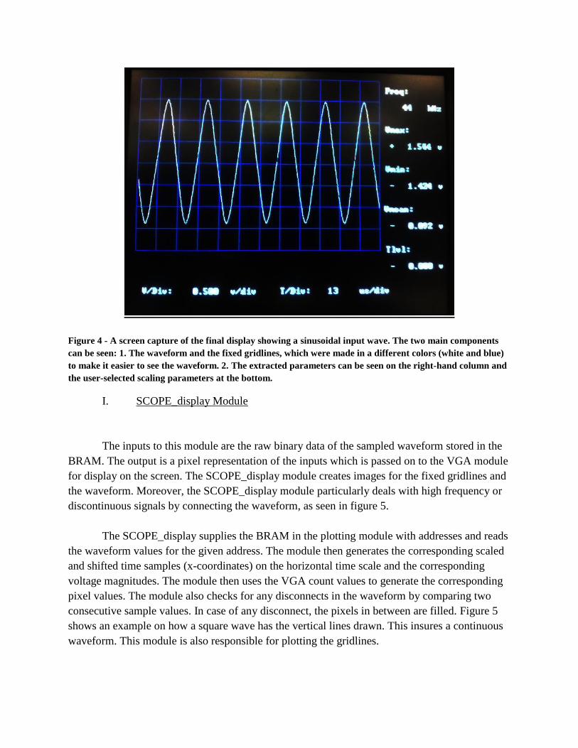
Figure 4 - A screen capture of the final display showing a sinusoidal input wave. The two main components
can be seen: 1. The waveform and the fixed gridlines, which were made in a different colors (white and blue)
to make it easier to see the waveform. 2. The extracted parameters can be seen on the right-hand column and
the user-selected scaling parameters at the bottom.
I. SCOPE_display Module
The inputs to this module are the raw binary data of the sampled waveform stored in the
BRAM. The output is a pixel representation of the inputs which is passed on to the VGA module
for display on the screen. The SCOPE_display module creates images for the fixed gridlines and
the waveform. Moreover, the SCOPE_display module particularly deals with high frequency or
discontinuous signals by connecting the waveform, as seen in figure 5.
The SCOPE_display supplies the BRAM in the plotting module with addresses and reads
the waveform values for the given address. The module then generates the corresponding scaled
and shifted time samples (x-coordinates) on the horizontal time scale and the corresponding
voltage magnitudes. The module then uses the VGA count values to generate the corresponding
pixel values. The module also checks for any disconnects in the waveform by comparing two
consecutive sample values. In case of any disconnect, the pixels in between are filled. Figure 5
shows an example on how a square wave has the vertical lines drawn. This insures a continuous
waveform. This module is also responsible for plotting the gridlines.

Figure 5 – A screen capture of the final display showing a square wave. A demonstration of how the
oscilloscope deals with high frequency inputs and discontinuous wave forms. If any discontinuities occur, the
algorithm connects the wave form samples. As seen above, the square wave jumps between +1.806 and -1.646
and the oscilloscope connects the waveform introducing the vertical edges which makes it look smoother.
The input to the display modules is provided by the plotting, scaling and computation
modules. Because all those modules were being created in parallel, in order to test the display it
was necessary to create a BRAM filled with samples. Therefore, a test module with samples
representing a square wave was created. This not only provided a known and stable waveform,
but also allowed to test for proper handling of discontinuities.
II. PARAM_display Module
The inputs to this module are the raw binary data representing the parameter values (of
the parameters listed previously). PARAM_display module creates images for the various
parameters including names, values, and units. The output is a pixel representation of the
parameters which is passed to the VGA module for display on the screen. The module also scales
the inputs to an appropriate order of magnitude (kilo-hertz, volts, micro-seconds, etc.) This is
achieved by shifting the binary input bits accordingly.

The PARAM_display module runs in parallel with the SCOPE_display module and
provides the corresponding parameter values for the displayed waveform. The parameter names
are simply displayed using the char-to-string display module. In order to display the values in a
convenient decimal form, the binary input is converted into a binary-coded decimal (BCD) form.
This is done with the help of the binary-to-bcd module. The main idea behind binary to BCD
conversion is to store a binary number as a series of hex digits. These hex digits range from zero
to nine and are represented with four bits per digit. They could be used as decimals even though
they are stored in a binary form.
There are several ways to implement a binary-to-BCD converter. We selected the double
dabble algorithm because it is one of the fastest and least computationally intensive methods.
This method is combinational and is implemented by shifting in a binary number one bit at a
time into an output register, starting at the most significant bit. Every time a binary bit is shifted
in, each decimal place is checked. If the hex value is greater than or equal to five, we add three.
By the time the entire binary number is shifted in, the output register will contain the converted
BCD number.
In order to display the BCD it is converted to a well formatted string. This is done by
mapping each four bit hex digit to an eight-bit ASCII equivalent. This string is then formatted to
accommodate for different number lengths and decimal points, and fed into the char-to-string
display module. This output is converted to pixel data with the help of a character map and sent
to the VGA module for display.
This module was mainly tested using the VGA display output. Different length strings
were used to test the char-to-string display module. The binary to BCD converter was tested
using a Model Simulator test bench. The test bench included different magnitude binary inputs
and checked we got the correct corresponding decimal outputs. The implemented algorithm,
inputs, and outputs were clearly defined which made it relatively simple to execute and debug.
The converter was tested on several values including the minimum and maximum values. We
also tested dynamic changes in binary inputs to insure the outputs changed smoothly. To achieve
that, we created a counter which ran through all possible input and output combinations. This
was important because our project require accurate and constantly changing measurements. The
results were satisfying.

Conclusions
As seen in the screen shots above, we met all the design goals and created a fully
functional oscilloscope. The scope is able to sample a voltage waveform input, extract minimum,
maximum, and average voltages from the waveform, accept user inputs for voltage, time, and the
trigger level, and plot the scaled waveform and parameters on the display.
The input stage initially suffered from noise issues. Much of this sampling noise stemmed
from ground loops caused by using digital outputs as enable signals, although it was assumed to
be a software issue which delayed fixing the problem. When these signals were moved to power
ground, most of the noise was eliminated, but this was unfortunately not done until very late in
the project. If a more thorough testing of the analog to digital board had been conducted initially,
significant time could have been saved which was wasted attempting to solve the problem in
code. Had this time been available, features such as auto-set could have been implemented.
In the display stage, initially we were trying to implement a frame buffer memory
element using the ZBT memory chips, which proved to be difficult due to the timing
specifications of the memory. It ended up being as effective, and substantially simpler, to have
no frame buffer and instead continuously read the samples from the BRAM. While the ZBT
would have been a more thorough solution, for our application the direct-to-VGA display
synthesis was sufficient. The ZBT effort used up a lot of time which could have been better
invested in executing the stretch goals.