agilent technologies esg family signal...
TRANSCRIPT

Serial Number Prefixes:
Service Guide
Agilent TechnologiesESG Family Signal Generators
Part No. E4400-90335
Printed in USADecember 2010
© Copyright 1999-2010 Agilent Technologies Inc.
(Affix Label Here)

ii

Contents
1. Initial Troubleshooting and RF Block DiagramsBefore You Begin Troubleshooting . . . . . . . . . . . . . . . . . . . . . . . . . . . . . . . . . . . . . . . . . . . . . .1-2Using this Service Guide to Troubleshoot. . . . . . . . . . . . . . . . . . . . . . . . . . . . . . . . . . . . . . . . .1-2Signal Generator Options . . . . . . . . . . . . . . . . . . . . . . . . . . . . . . . . . . . . . . . . . . . . . . . . . . . . .1-3Contacting Agilent Technologies . . . . . . . . . . . . . . . . . . . . . . . . . . . . . . . . . . . . . . . . . . . . . . . .1-8
Check the Basics before Contacting Agilent Technologies . . . . . . . . . . . . . . . . . . . . . . . . . .1-8Review the Warranty . . . . . . . . . . . . . . . . . . . . . . . . . . . . . . . . . . . . . . . . . . . . . . . . . . . . . . .1-8Calling Agilent Technologies Sales and Service Offices . . . . . . . . . . . . . . . . . . . . . . . . . . . .1-8Returning Your Signal Generator for Service . . . . . . . . . . . . . . . . . . . . . . . . . . . . . . . . . . .1-10
Equipment Required for Troubleshooting . . . . . . . . . . . . . . . . . . . . . . . . . . . . . . . . . . . . . . .1-11Initial Troubleshooting . . . . . . . . . . . . . . . . . . . . . . . . . . . . . . . . . . . . . . . . . . . . . . . . . . . . . .1-12
Step 1: Observe the Front and Rear Panel LEDs . . . . . . . . . . . . . . . . . . . . . . . . . . . . . . . .1-12Step 2: Power On the Signal Generator and Check for Error Messages . . . . . . . . . . . . . .1-13Step 3: Functional Check the Front Panel Keys and Display . . . . . . . . . . . . . . . . . . . . . .1-14Step 4: Visually Check the Individual Voltage Supplies. . . . . . . . . . . . . . . . . . . . . . . . . . .1-15Step 5: Measure the Individual Voltage Supplies . . . . . . . . . . . . . . . . . . . . . . . . . . . . . . . .1-16Step 6: Isolate the Failed Assembly . . . . . . . . . . . . . . . . . . . . . . . . . . . . . . . . . . . . . . . . . . .1-19Step 7: Check for Basic CPU Functionality. . . . . . . . . . . . . . . . . . . . . . . . . . . . . . . . . . . . .1-21
Additional Information for Troubleshooting the ESG-AP and ESG-DP Series . . . . . . . . . .1-23ESG-A Series RF Block Diagram (Standard & Option 1E6) . . . . . . . . . . . . . . . . . . . . . . . . .1-25ESG-D Series RF Block Diagram . . . . . . . . . . . . . . . . . . . . . . . . . . . . . . . . . . . . . . . . . . . . . .1-27ESG-D Series RF Block Diagram (Options UN3 & UN4) . . . . . . . . . . . . . . . . . . . . . . . . . . .1-29ESG-D Series RF Block Diagram (Option UN8 or UN9) Rev C or D . . . . . . . . . . . . . . . . . .1-31. . . . . . . . . . . . . . . . . . . . . . . . . . . . . . . . . . . . . . . . . . . . . . . . . . . . . . . . . . . . . . . . . . . . . . . . . .1-32ESG-D Series RF Block Diagram (Options UN8 & UN9) Rev B . . . . . . . . . . . . . . . . . . . . . .1-35ESG-D Series RF Block Diagram (Option UND) . . . . . . . . . . . . . . . . . . . . . . . . . . . . . . . . . .1-37ESG-D Series RF Block Diagram (Option UN7, UN8/UN9, & 300) . . . . . . . . . . . . . . . . . . .1-39ESG-AP Series RF Block Diagram (Standard & Option 1E6) . . . . . . . . . . . . . . . . . . . . . . . .1-41ESG-DP Series RF Block Diagram . . . . . . . . . . . . . . . . . . . . . . . . . . . . . . . . . . . . . . . . . . . . .1-43ESG-DP Series RF Block Diagram (Option UN7) . . . . . . . . . . . . . . . . . . . . . . . . . . . . . . . . .1-45ESG-DP Series RF Block Diagram (Options UN8 & UN9) . . . . . . . . . . . . . . . . . . . . . . . . . .1-47ESG-DP Series RF Block Diagram (Option UND) . . . . . . . . . . . . . . . . . . . . . . . . . . . . . . . . .1-49Blue Repair Tags . . . . . . . . . . . . . . . . . . . . . . . . . . . . . . . . . . . . . . . . . . . . . . . . . . . . . . . . . . .1-51
2. Assembly-Level Troubleshooting with Block DiagramsBefore You Begin Troubleshooting . . . . . . . . . . . . . . . . . . . . . . . . . . . . . . . . . . . . . . . . . . . . . .2-2Using this Chapter with Service Software . . . . . . . . . . . . . . . . . . . . . . . . . . . . . . . . . . . . . . . .2-2A5 Dual Arbitrary Waveform Generator Block Diagram (Option UND) . . . . . . . . . . . . . . . .2-5A6 Bit Error Rate Test Block Diagram (Option UN7) . . . . . . . . . . . . . . . . . . . . . . . . . . . . . . .2-7A7 Baseband Generator Block Diagram (Options UN3 & UN4) . . . . . . . . . . . . . . . . . . . . . . .2-9A7 DBMIC Baseband Generator Block Diagram (Options UN8 & UN9) . . . . . . . . . . . . . . .2-11A8 Data Generator Block Diagram (Options UN3 & UN4) . . . . . . . . . . . . . . . . . . . . . . . . . .2-13A8 Data Generator - Rev. A & B Block Diagram (Options UN8 & UN9) . . . . . . . . . . . . . . .2-15A8 Flex Data Generator - Rev. C & D Block Diagram (Options UN8 & UN9) . . . . . . . . . . .2-17A9 Output ABUS Nodes (ESG-A Series) . . . . . . . . . . . . . . . . . . . . . . . . . . . . . . . . . . . . . . . .2-19A9 Output Block Diagram (ESG-A Series) . . . . . . . . . . . . . . . . . . . . . . . . . . . . . . . . . . . . . . .2-21A9 Output ABUS Nodes (ESG-D Series) . . . . . . . . . . . . . . . . . . . . . . . . . . . . . . . . . . . . . . . .2-23A9 Output ABUS Nodes (ESG-AP, & ESG-DP Series). . . . . . . . . . . . . . . . . . . . . . . . . . . . . .2-25A9 Output Block Diagram (ESG-D, ESG-AP, & ESG-DP Series) . . . . . . . . . . . . . . . . . . . . .2-27A11 Reference ABUS Nodes (ESG-A & ESG-D Series) . . . . . . . . . . . . . . . . . . . . . . . . . . . . .2-29A11 Reference Block Diagram (ESG-A & ESG-D Series) . . . . . . . . . . . . . . . . . . . . . . . . . . .2-31
iii

Contents
A11 Reference ABUS Nodes (ESG-AP & ESG-DP Series) . . . . . . . . . . . . . . . . . . . . . . . . . . 2-33A11 Reference Block Diagram (ESG-AP & ESG-DP Series). . . . . . . . . . . . . . . . . . . . . . . . . 2-35A12 Synthesizer/Doubler ABUS Nodes (ESG-A & ESG-D Series) . . . . . . . . . . . . . . . . . . . . 2-37A12 Synthesizer/Doubler Block Diagram (ESG-A & ESG-D Series) . . . . . . . . . . . . . . . . . . 2-39A14 CPU/Motherboard ABUS Nodes . . . . . . . . . . . . . . . . . . . . . . . . . . . . . . . . . . . . . . . . . . . 2-41A14 CPU/Motherboard Block Diagram (1 of 2) . . . . . . . . . . . . . . . . . . . . . . . . . . . . . . . . . . . 2-43A14 CPU/Motherboard Block Diagram (2 of 2) . . . . . . . . . . . . . . . . . . . . . . . . . . . . . . . . . . . 2-45A20 Downconvertor Block Diagram (Option 300) . . . . . . . . . . . . . . . . . . . . . . . . . . . . . . . . . 2-47A21 Demodulator Block Diagram (Option 300) . . . . . . . . . . . . . . . . . . . . . . . . . . . . . . . . . . . 2-49A22 YIG Driver ABUS Nodes (ESG-AP & ESG-DP Series) . . . . . . . . . . . . . . . . . . . . . . . . . 2-51A22 YIG Driver Block Diagram (ESG-AP & ESG-DP Series). . . . . . . . . . . . . . . . . . . . . . . . 2-53A23 Sampler ABUS Nodes (ESG-AP & ESG-DP Series) . . . . . . . . . . . . . . . . . . . . . . . . . . . 2-55A23 Sampler Block Diagram (ESG-AP & ESG-DP Series) . . . . . . . . . . . . . . . . . . . . . . . . . . 2-57A24 Frac-N/Divider ABUS Nodes (ESG-AP & ESG-DP Series . . . . . . . . . . . . . . . . . . . . . . 2-59A24 Frac-N/Divider Block Diagram (ESG-AP & ESG-DP Series . . . . . . . . . . . . . . . . . . . . . 2-61AT1 Electronic Attenuator/RPP Block Diagram . . . . . . . . . . . . . . . . . . . . . . . . . . . . . . . . . . 2-63AT1 Mechanical Attenuator and A19 RPP Block Diagram (Option UNB) . . . . . . . . . . . . . 2-65ESG-A Series Power Supply and Ground Interconnects Block Diagram. . . . . . . . . . . . . . . 2-67ESG-D Series Power Supply and Ground Interconnects Block Diagram (1 of 2) . . . . . . . . 2-69ESG-D Series Power Supply and Ground Interconnects Block Diagram (2 of 2) . . . . . . . . 2-71ESG-A Series Modulation and Signal Interconnects Block Diagram. . . . . . . . . . . . . . . . . . 2-73ESG-D Series Modulation and Signal Interconnects Block Diagram (1 of 2) . . . . . . . . . . . 2-75ESG-D Series Modulation and Signal Interconnects Block Diagram (2 of 2) . . . . . . . . . . . 2-77
3. Replaceable Parts (ESG-A and ESG-D Series)Ordering Information . . . . . . . . . . . . . . . . . . . . . . . . . . . . . . . . . . . . . . . . . . . . . . . . . . . . . . . . 3-2
Call (800) 227-8164 to Order Parts Fast (U.S. Only) . . . . . . . . . . . . . . . . . . . . . . . . . . . . . . 3-2Save Money with Rebuilt-Exchange Assemblies . . . . . . . . . . . . . . . . . . . . . . . . . . . . . . . . . . . 3-3
Shipping the Defective Assembly Back to Agilent Technologies . . . . . . . . . . . . . . . . . . . . . 3-4Abbreviations Used in Part Descriptions . . . . . . . . . . . . . . . . . . . . . . . . . . . . . . . . . . . . . . . . . 3-5Major Assemblies. . . . . . . . . . . . . . . . . . . . . . . . . . . . . . . . . . . . . . . . . . . . . . . . . . . . . . . . . . . . 3-7
Top View . . . . . . . . . . . . . . . . . . . . . . . . . . . . . . . . . . . . . . . . . . . . . . . . . . . . . . . . . . . . . . . . . 3-8Top View (ESG-D Series - Option 300) . . . . . . . . . . . . . . . . . . . . . . . . . . . . . . . . . . . . . . . . 3-10Right Side Assemblies . . . . . . . . . . . . . . . . . . . . . . . . . . . . . . . . . . . . . . . . . . . . . . . . . . . . . 3-12Disassembled Front Panel View . . . . . . . . . . . . . . . . . . . . . . . . . . . . . . . . . . . . . . . . . . . . . 3-13Inside Rear Panel View . . . . . . . . . . . . . . . . . . . . . . . . . . . . . . . . . . . . . . . . . . . . . . . . . . . . 3-14
Cables . . . . . . . . . . . . . . . . . . . . . . . . . . . . . . . . . . . . . . . . . . . . . . . . . . . . . . . . . . . . . . . . . . . . 3-15Top View (ESG-A Series) . . . . . . . . . . . . . . . . . . . . . . . . . . . . . . . . . . . . . . . . . . . . . . . . . . . 3-16Top View (ESG-D Series - Options UN3/4, UN7) . . . . . . . . . . . . . . . . . . . . . . . . . . . . . . . . 3-18Top View (ESG-D Series - Options UN7, UN8) . . . . . . . . . . . . . . . . . . . . . . . . . . . . . . . . . 3-20Top View (ESG-D Series - Option UND) . . . . . . . . . . . . . . . . . . . . . . . . . . . . . . . . . . . . . . . 3-22Top View (ESG-D Series - Options UN3/4, UN7 with 1EM) . . . . . . . . . . . . . . . . . . . . . . . 3-24Top View (ESG-D Series - Options UN7, UN8 with 1EM). . . . . . . . . . . . . . . . . . . . . . . . . 3-26Top View (ESG-D Series - Options UN7, UN8, UND) . . . . . . . . . . . . . . . . . . . . . . . . . . . . 3-28Top View (ESG-D Series - Option UND with 1EM) . . . . . . . . . . . . . . . . . . . . . . . . . . . . . . 3-30Top View (ESG-D Series - Option 300) . . . . . . . . . . . . . . . . . . . . . . . . . . . . . . . . . . . . . . . . 3-32Inside Front Panel View. . . . . . . . . . . . . . . . . . . . . . . . . . . . . . . . . . . . . . . . . . . . . . . . . . . . 3-34Electronic Attenuator/RPP View. . . . . . . . . . . . . . . . . . . . . . . . . . . . . . . . . . . . . . . . . . . . . 3-36
iv

Contents
Electronic Attenuator/RPP View (with Option 1EM) . . . . . . . . . . . . . . . . . . . . . . . . . . . . .3-38Mechanical Attenuator View (Option UNB) . . . . . . . . . . . . . . . . . . . . . . . . . . . . . . . . . . . .3-40Mechanical Attenuator View (Option UNB with 1EM) . . . . . . . . . . . . . . . . . . . . . . . . . . .3-42Pulse Modulator View (Option 1E6) . . . . . . . . . . . . . . . . . . . . . . . . . . . . . . . . . . . . . . . . . .3-44
Hardware and Other Instrument Parts . . . . . . . . . . . . . . . . . . . . . . . . . . . . . . . . . . . . . . . . .3-45Top View . . . . . . . . . . . . . . . . . . . . . . . . . . . . . . . . . . . . . . . . . . . . . . . . . . . . . . . . . . . . . . . .3-46Downconvertor View (Option 300) . . . . . . . . . . . . . . . . . . . . . . . . . . . . . . . . . . . . . . . . . . . .3-48Disassembled Mechanical Attenuator View (Option UNB) . . . . . . . . . . . . . . . . . . . . . . . .3-49Disassembled Pulse Modulator View (Option 1E6). . . . . . . . . . . . . . . . . . . . . . . . . . . . . . .3-50Disassembled Pulse Modulator View (Option 1E6/UNB) . . . . . . . . . . . . . . . . . . . . . . . . . .3-51Front Panel View (ESG-A Series). . . . . . . . . . . . . . . . . . . . . . . . . . . . . . . . . . . . . . . . . . . . .3-52Front Panel View (ESG-D Series) . . . . . . . . . . . . . . . . . . . . . . . . . . . . . . . . . . . . . . . . . . . .3-54Disassembled Front-Panel View. . . . . . . . . . . . . . . . . . . . . . . . . . . . . . . . . . . . . . . . . . . . . .3-56Daughterboard Card Cage View . . . . . . . . . . . . . . . . . . . . . . . . . . . . . . . . . . . . . . . . . . . . .3-58Inside Rear-Panel View. . . . . . . . . . . . . . . . . . . . . . . . . . . . . . . . . . . . . . . . . . . . . . . . . . . . .3-59Rear-Panel View (ESG-A Series) . . . . . . . . . . . . . . . . . . . . . . . . . . . . . . . . . . . . . . . . . . . . .3-60Rear-Panel View (ESG-A Series - Option 1EM) . . . . . . . . . . . . . . . . . . . . . . . . . . . . . . . . .3-62Rear-Panel View (ESG-D Series) . . . . . . . . . . . . . . . . . . . . . . . . . . . . . . . . . . . . . . . . . . . . .3-64Rear Panel View (ESG-D Series - Option 1EM) . . . . . . . . . . . . . . . . . . . . . . . . . . . . . . . . .3-66Instrument Chassis with Top and Right-Side Hardware . . . . . . . . . . . . . . . . . . . . . . . . . .3-68Power Supply Shield and Left-Side Hardware . . . . . . . . . . . . . . . . . . . . . . . . . . . . . . . . . .3-70Motherboard and Bottom-Side Hardware . . . . . . . . . . . . . . . . . . . . . . . . . . . . . . . . . . . . . .3-71Instrument Cover and Associated Parts . . . . . . . . . . . . . . . . . . . . . . . . . . . . . . . . . . . . . . .3-72
Miscellaneous . . . . . . . . . . . . . . . . . . . . . . . . . . . . . . . . . . . . . . . . . . . . . . . . . . . . . . . . . . . . . .3-74Accessories. . . . . . . . . . . . . . . . . . . . . . . . . . . . . . . . . . . . . . . . . . . . . . . . . . . . . . . . . . . . . . .3-74Documentation . . . . . . . . . . . . . . . . . . . . . . . . . . . . . . . . . . . . . . . . . . . . . . . . . . . . . . . . . . .3-75Electrostatic Discharge (ESD) Protective Supplies. . . . . . . . . . . . . . . . . . . . . . . . . . . . . . .3-78Upgrade and Retrofit Kits . . . . . . . . . . . . . . . . . . . . . . . . . . . . . . . . . . . . . . . . . . . . . . . . . .3-78
4. Replaceable Parts (ESG-AP and ESG-DP Series)Ordering Information. . . . . . . . . . . . . . . . . . . . . . . . . . . . . . . . . . . . . . . . . . . . . . . . . . . . . . . . .4-2
Call (800) 227-8164 to Order Parts Fast (U.S. Only). . . . . . . . . . . . . . . . . . . . . . . . . . . . . . .4-2Save Money with Rebuilt-Exchange Assemblies . . . . . . . . . . . . . . . . . . . . . . . . . . . . . . . . . . .4-3
Shipping the Defective Assembly Back to Agilent Technologies . . . . . . . . . . . . . . . . . . . . .4-4Abbreviations Used in Part Descriptions . . . . . . . . . . . . . . . . . . . . . . . . . . . . . . . . . . . . . . . . .4-5Major Assemblies . . . . . . . . . . . . . . . . . . . . . . . . . . . . . . . . . . . . . . . . . . . . . . . . . . . . . . . . . . . .4-7
Top View . . . . . . . . . . . . . . . . . . . . . . . . . . . . . . . . . . . . . . . . . . . . . . . . . . . . . . . . . . . . . . . . .4-8Right Side Assemblies . . . . . . . . . . . . . . . . . . . . . . . . . . . . . . . . . . . . . . . . . . . . . . . . . . . . .4-10Disassembled Front Panel View. . . . . . . . . . . . . . . . . . . . . . . . . . . . . . . . . . . . . . . . . . . . . .4-11Inside Rear Panel View. . . . . . . . . . . . . . . . . . . . . . . . . . . . . . . . . . . . . . . . . . . . . . . . . . . . .4-12
Cables . . . . . . . . . . . . . . . . . . . . . . . . . . . . . . . . . . . . . . . . . . . . . . . . . . . . . . . . . . . . . . . . . . . .4-13Top View . . . . . . . . . . . . . . . . . . . . . . . . . . . . . . . . . . . . . . . . . . . . . . . . . . . . . . . . . . . . . . . .4-14Top View (ESG-DP Series - Options UN7, UN8). . . . . . . . . . . . . . . . . . . . . . . . . . . . . . . . .4-16Top View (ESG-DP Series - Option UND) . . . . . . . . . . . . . . . . . . . . . . . . . . . . . . . . . . . . . .4-18Top View (ESG-DP Series - Options UN7, UN8 with 1EM) . . . . . . . . . . . . . . . . . . . . . . . .4-20Top View (ESG-DP Series - Options UN7, UN8, UND) . . . . . . . . . . . . . . . . . . . . . . . . . . .4-22Top View (ESG-DP Series - Option UND with 1EM) . . . . . . . . . . . . . . . . . . . . . . . . . . . . .4-24Side View — YIG Driver Assembly . . . . . . . . . . . . . . . . . . . . . . . . . . . . . . . . . . . . . . . . . . .4-26
v

Contents
Inside Front Panel View. . . . . . . . . . . . . . . . . . . . . . . . . . . . . . . . . . . . . . . . . . . . . . . . . . . . 4-28Electronic Attenuator/RPP View. . . . . . . . . . . . . . . . . . . . . . . . . . . . . . . . . . . . . . . . . . . . . 4-30Electronic Attenuator/RPP View (with Option 1EM). . . . . . . . . . . . . . . . . . . . . . . . . . . . . 4-32Mechanical Attenuator View (Option UNB) . . . . . . . . . . . . . . . . . . . . . . . . . . . . . . . . . . . . 4-34Mechanical Attenuator View (Option UNB with 1EM) . . . . . . . . . . . . . . . . . . . . . . . . . . . 4-36Pulse Modulator View (Option 1E6) . . . . . . . . . . . . . . . . . . . . . . . . . . . . . . . . . . . . . . . . . . 4-38
Hardware and Other Instrument Parts . . . . . . . . . . . . . . . . . . . . . . . . . . . . . . . . . . . . . . . . . 4-39Top View . . . . . . . . . . . . . . . . . . . . . . . . . . . . . . . . . . . . . . . . . . . . . . . . . . . . . . . . . . . . . . . . 4-40YIG Driver View. . . . . . . . . . . . . . . . . . . . . . . . . . . . . . . . . . . . . . . . . . . . . . . . . . . . . . . . . . 4-42Disassembled Mechanical Attenuator View (Option UNB) . . . . . . . . . . . . . . . . . . . . . . . . 4-43Disassembled Pulse Modulator View (Option 1E6) . . . . . . . . . . . . . . . . . . . . . . . . . . . . . . 4-44Disassembled Pulse Modulator View (Option 1E6/UNB) . . . . . . . . . . . . . . . . . . . . . . . . . 4-45Front Panel View (ESG-AP Series) . . . . . . . . . . . . . . . . . . . . . . . . . . . . . . . . . . . . . . . . . . . 4-46Front Panel View (ESG-DP Series) . . . . . . . . . . . . . . . . . . . . . . . . . . . . . . . . . . . . . . . . . . . 4-48Disassembled Front-Panel View . . . . . . . . . . . . . . . . . . . . . . . . . . . . . . . . . . . . . . . . . . . . . 4-50Daughterboard Card Cage View . . . . . . . . . . . . . . . . . . . . . . . . . . . . . . . . . . . . . . . . . . . . . 4-52Inside Rear-Panel View . . . . . . . . . . . . . . . . . . . . . . . . . . . . . . . . . . . . . . . . . . . . . . . . . . . . 4-53Rear-Panel View (ESG-AP Series). . . . . . . . . . . . . . . . . . . . . . . . . . . . . . . . . . . . . . . . . . . . 4-54Rear-Panel View (ESG-AP Series - Option 1EM) . . . . . . . . . . . . . . . . . . . . . . . . . . . . . . . . 4-56Rear-Panel View (ESG-DP Series) . . . . . . . . . . . . . . . . . . . . . . . . . . . . . . . . . . . . . . . . . . . 4-58Rear Panel View (ESG-DP Series - Option 1EM). . . . . . . . . . . . . . . . . . . . . . . . . . . . . . . . 4-60Instrument Chassis with Top and Right-Side Hardware. . . . . . . . . . . . . . . . . . . . . . . . . . 4-62Power Supply Shield and Left-Side Hardware . . . . . . . . . . . . . . . . . . . . . . . . . . . . . . . . . . 4-64Motherboard and Bottom-Side Hardware. . . . . . . . . . . . . . . . . . . . . . . . . . . . . . . . . . . . . . 4-65Instrument Cover and Associated Parts . . . . . . . . . . . . . . . . . . . . . . . . . . . . . . . . . . . . . . . 4-66
Miscellaneous. . . . . . . . . . . . . . . . . . . . . . . . . . . . . . . . . . . . . . . . . . . . . . . . . . . . . . . . . . . . . . 4-68Accessories . . . . . . . . . . . . . . . . . . . . . . . . . . . . . . . . . . . . . . . . . . . . . . . . . . . . . . . . . . . . . . 4-68Documentation . . . . . . . . . . . . . . . . . . . . . . . . . . . . . . . . . . . . . . . . . . . . . . . . . . . . . . . . . . . 4-69Electrostatic Discharge (ESD) Protective Supplies . . . . . . . . . . . . . . . . . . . . . . . . . . . . . . 4-72Upgrade and Retrofit Kits . . . . . . . . . . . . . . . . . . . . . . . . . . . . . . . . . . . . . . . . . . . . . . . . . . 4-72
5. Assembly ReplacementBefore You Replace an Assembly . . . . . . . . . . . . . . . . . . . . . . . . . . . . . . . . . . . . . . . . . . . . . . . 5-2After Replacing an Assembly . . . . . . . . . . . . . . . . . . . . . . . . . . . . . . . . . . . . . . . . . . . . . . . . . . 5-2Assemblies That You Can Replace . . . . . . . . . . . . . . . . . . . . . . . . . . . . . . . . . . . . . . . . . . . . . . 5-3A1 Front Panel Board . . . . . . . . . . . . . . . . . . . . . . . . . . . . . . . . . . . . . . . . . . . . . . . . . . . . . . . . 5-4
Tools Required . . . . . . . . . . . . . . . . . . . . . . . . . . . . . . . . . . . . . . . . . . . . . . . . . . . . . . . . . . . . 5-4Removal . . . . . . . . . . . . . . . . . . . . . . . . . . . . . . . . . . . . . . . . . . . . . . . . . . . . . . . . . . . . . . . . . 5-4Replacement . . . . . . . . . . . . . . . . . . . . . . . . . . . . . . . . . . . . . . . . . . . . . . . . . . . . . . . . . . . . . . 5-4
A2 Display . . . . . . . . . . . . . . . . . . . . . . . . . . . . . . . . . . . . . . . . . . . . . . . . . . . . . . . . . . . . . . . . . 5-6Tools Required . . . . . . . . . . . . . . . . . . . . . . . . . . . . . . . . . . . . . . . . . . . . . . . . . . . . . . . . . . . . 5-6Removal . . . . . . . . . . . . . . . . . . . . . . . . . . . . . . . . . . . . . . . . . . . . . . . . . . . . . . . . . . . . . . . . . 5-6Replacement . . . . . . . . . . . . . . . . . . . . . . . . . . . . . . . . . . . . . . . . . . . . . . . . . . . . . . . . . . . . . . 5-6
A2DS1 Fluorescent Lamp . . . . . . . . . . . . . . . . . . . . . . . . . . . . . . . . . . . . . . . . . . . . . . . . . . . . . 5-9Tools Required . . . . . . . . . . . . . . . . . . . . . . . . . . . . . . . . . . . . . . . . . . . . . . . . . . . . . . . . . . . . 5-9Removal . . . . . . . . . . . . . . . . . . . . . . . . . . . . . . . . . . . . . . . . . . . . . . . . . . . . . . . . . . . . . . . . . 5-9Replacement . . . . . . . . . . . . . . . . . . . . . . . . . . . . . . . . . . . . . . . . . . . . . . . . . . . . . . . . . . . . . . 5-9
A3 Inverter. . . . . . . . . . . . . . . . . . . . . . . . . . . . . . . . . . . . . . . . . . . . . . . . . . . . . . . . . . . . . . . . 5-10Tools Required . . . . . . . . . . . . . . . . . . . . . . . . . . . . . . . . . . . . . . . . . . . . . . . . . . . . . . . . . . . 5-10Removal . . . . . . . . . . . . . . . . . . . . . . . . . . . . . . . . . . . . . . . . . . . . . . . . . . . . . . . . . . . . . . . . 5-10
vi
Contents
Replacement . . . . . . . . . . . . . . . . . . . . . . . . . . . . . . . . . . . . . . . . . . . . . . . . . . . . . . . . . . . . .5-10A4 Power Supply . . . . . . . . . . . . . . . . . . . . . . . . . . . . . . . . . . . . . . . . . . . . . . . . . . . . . . . . . . .5-12
Tools Required. . . . . . . . . . . . . . . . . . . . . . . . . . . . . . . . . . . . . . . . . . . . . . . . . . . . . . . . . . . .5-12Removal . . . . . . . . . . . . . . . . . . . . . . . . . . . . . . . . . . . . . . . . . . . . . . . . . . . . . . . . . . . . . . . . .5-12Replacement . . . . . . . . . . . . . . . . . . . . . . . . . . . . . . . . . . . . . . . . . . . . . . . . . . . . . . . . . . . . .5-12
A4 Power Supply (with Option 1EM) . . . . . . . . . . . . . . . . . . . . . . . . . . . . . . . . . . . . . . . . . . .5-15Tools Required. . . . . . . . . . . . . . . . . . . . . . . . . . . . . . . . . . . . . . . . . . . . . . . . . . . . . . . . . . . .5-15Removal . . . . . . . . . . . . . . . . . . . . . . . . . . . . . . . . . . . . . . . . . . . . . . . . . . . . . . . . . . . . . . . . .5-15Replacement . . . . . . . . . . . . . . . . . . . . . . . . . . . . . . . . . . . . . . . . . . . . . . . . . . . . . . . . . . . . .5-15
A14 CPU/Motherboard. . . . . . . . . . . . . . . . . . . . . . . . . . . . . . . . . . . . . . . . . . . . . . . . . . . . . . .5-18Tools Required. . . . . . . . . . . . . . . . . . . . . . . . . . . . . . . . . . . . . . . . . . . . . . . . . . . . . . . . . . . .5-18Removal . . . . . . . . . . . . . . . . . . . . . . . . . . . . . . . . . . . . . . . . . . . . . . . . . . . . . . . . . . . . . . . . .5-18Replacement . . . . . . . . . . . . . . . . . . . . . . . . . . . . . . . . . . . . . . . . . . . . . . . . . . . . . . . . . . . . .5-20
A14BT1 Battery . . . . . . . . . . . . . . . . . . . . . . . . . . . . . . . . . . . . . . . . . . . . . . . . . . . . . . . . . . . .5-24Tools Required. . . . . . . . . . . . . . . . . . . . . . . . . . . . . . . . . . . . . . . . . . . . . . . . . . . . . . . . . . . .5-24Removal . . . . . . . . . . . . . . . . . . . . . . . . . . . . . . . . . . . . . . . . . . . . . . . . . . . . . . . . . . . . . . . . .5-24Replacement . . . . . . . . . . . . . . . . . . . . . . . . . . . . . . . . . . . . . . . . . . . . . . . . . . . . . . . . . . . . .5-24
A14Q501 Transistor . . . . . . . . . . . . . . . . . . . . . . . . . . . . . . . . . . . . . . . . . . . . . . . . . . . . . . . . .5-26Tools Required. . . . . . . . . . . . . . . . . . . . . . . . . . . . . . . . . . . . . . . . . . . . . . . . . . . . . . . . . . . .5-26Removal . . . . . . . . . . . . . . . . . . . . . . . . . . . . . . . . . . . . . . . . . . . . . . . . . . . . . . . . . . . . . . . . .5-26Replacement . . . . . . . . . . . . . . . . . . . . . . . . . . . . . . . . . . . . . . . . . . . . . . . . . . . . . . . . . . . . .5-26
A15 Daughterboard . . . . . . . . . . . . . . . . . . . . . . . . . . . . . . . . . . . . . . . . . . . . . . . . . . . . . . . . .5-28Tools Required. . . . . . . . . . . . . . . . . . . . . . . . . . . . . . . . . . . . . . . . . . . . . . . . . . . . . . . . . . . .5-28Removal . . . . . . . . . . . . . . . . . . . . . . . . . . . . . . . . . . . . . . . . . . . . . . . . . . . . . . . . . . . . . . . . .5-28Replacement . . . . . . . . . . . . . . . . . . . . . . . . . . . . . . . . . . . . . . . . . . . . . . . . . . . . . . . . . . . . .5-30
A16 Line Module . . . . . . . . . . . . . . . . . . . . . . . . . . . . . . . . . . . . . . . . . . . . . . . . . . . . . . . . . . .5-32Tools Required. . . . . . . . . . . . . . . . . . . . . . . . . . . . . . . . . . . . . . . . . . . . . . . . . . . . . . . . . . . .5-32Removal . . . . . . . . . . . . . . . . . . . . . . . . . . . . . . . . . . . . . . . . . . . . . . . . . . . . . . . . . . . . . . . . .5-32Replacement . . . . . . . . . . . . . . . . . . . . . . . . . . . . . . . . . . . . . . . . . . . . . . . . . . . . . . . . . . . . .5-32
A17 and A18 Rear Panel Interface Boards . . . . . . . . . . . . . . . . . . . . . . . . . . . . . . . . . . . . . . .5-34 Tools Required . . . . . . . . . . . . . . . . . . . . . . . . . . . . . . . . . . . . . . . . . . . . . . . . . . . . . . . . . . .5-34Removal . . . . . . . . . . . . . . . . . . . . . . . . . . . . . . . . . . . . . . . . . . . . . . . . . . . . . . . . . . . . . . . . .5-34Replacement . . . . . . . . . . . . . . . . . . . . . . . . . . . . . . . . . . . . . . . . . . . . . . . . . . . . . . . . . . . . .5-34
A19 Reverse Power Protection (RPP) . . . . . . . . . . . . . . . . . . . . . . . . . . . . . . . . . . . . . . . . . . .5-36Tools Required. . . . . . . . . . . . . . . . . . . . . . . . . . . . . . . . . . . . . . . . . . . . . . . . . . . . . . . . . . . .5-36Removal . . . . . . . . . . . . . . . . . . . . . . . . . . . . . . . . . . . . . . . . . . . . . . . . . . . . . . . . . . . . . . . . .5-36Replacement . . . . . . . . . . . . . . . . . . . . . . . . . . . . . . . . . . . . . . . . . . . . . . . . . . . . . . . . . . . . .5-37
A20 Downconvertor . . . . . . . . . . . . . . . . . . . . . . . . . . . . . . . . . . . . . . . . . . . . . . . . . . . . . . . . .5-39Tools Required. . . . . . . . . . . . . . . . . . . . . . . . . . . . . . . . . . . . . . . . . . . . . . . . . . . . . . . . . . . .5-39Removal . . . . . . . . . . . . . . . . . . . . . . . . . . . . . . . . . . . . . . . . . . . . . . . . . . . . . . . . . . . . . . . . .5-39Replacement . . . . . . . . . . . . . . . . . . . . . . . . . . . . . . . . . . . . . . . . . . . . . . . . . . . . . . . . . . . . .5-39
A22 YIG Driver. . . . . . . . . . . . . . . . . . . . . . . . . . . . . . . . . . . . . . . . . . . . . . . . . . . . . . . . . . . . .5-40Tools Required. . . . . . . . . . . . . . . . . . . . . . . . . . . . . . . . . . . . . . . . . . . . . . . . . . . . . . . . . . . .5-40Removal . . . . . . . . . . . . . . . . . . . . . . . . . . . . . . . . . . . . . . . . . . . . . . . . . . . . . . . . . . . . . . . . .5-40Replacement . . . . . . . . . . . . . . . . . . . . . . . . . . . . . . . . . . . . . . . . . . . . . . . . . . . . . . . . . . . . .5-40
A25 Pulse Modulator . . . . . . . . . . . . . . . . . . . . . . . . . . . . . . . . . . . . . . . . . . . . . . . . . . . . . . . .5-41Tools Required. . . . . . . . . . . . . . . . . . . . . . . . . . . . . . . . . . . . . . . . . . . . . . . . . . . . . . . . . . . .5-41Removal . . . . . . . . . . . . . . . . . . . . . . . . . . . . . . . . . . . . . . . . . . . . . . . . . . . . . . . . . . . . . . . . .5-41Replacement . . . . . . . . . . . . . . . . . . . . . . . . . . . . . . . . . . . . . . . . . . . . . . . . . . . . . . . . . . . . .5-41
vii

Contents
A25 Pulse Modulator (with Option UNB) . . . . . . . . . . . . . . . . . . . . . . . . . . . . . . . . . . . . . . . 5-43Tools Required . . . . . . . . . . . . . . . . . . . . . . . . . . . . . . . . . . . . . . . . . . . . . . . . . . . . . . . . . . . 5-43Removal . . . . . . . . . . . . . . . . . . . . . . . . . . . . . . . . . . . . . . . . . . . . . . . . . . . . . . . . . . . . . . . . 5-43Replacement . . . . . . . . . . . . . . . . . . . . . . . . . . . . . . . . . . . . . . . . . . . . . . . . . . . . . . . . . . . . . 5-44
AT1 Electronic Attenuator/RPP . . . . . . . . . . . . . . . . . . . . . . . . . . . . . . . . . . . . . . . . . . . . . . . 5-46Tools Required . . . . . . . . . . . . . . . . . . . . . . . . . . . . . . . . . . . . . . . . . . . . . . . . . . . . . . . . . . . 5-46Removal . . . . . . . . . . . . . . . . . . . . . . . . . . . . . . . . . . . . . . . . . . . . . . . . . . . . . . . . . . . . . . . . 5-46Replacement . . . . . . . . . . . . . . . . . . . . . . . . . . . . . . . . . . . . . . . . . . . . . . . . . . . . . . . . . . . . . 5-46
AT1 Mechanical Attenuator . . . . . . . . . . . . . . . . . . . . . . . . . . . . . . . . . . . . . . . . . . . . . . . . . . 5-48Tools Required . . . . . . . . . . . . . . . . . . . . . . . . . . . . . . . . . . . . . . . . . . . . . . . . . . . . . . . . . . . 5-48Removal . . . . . . . . . . . . . . . . . . . . . . . . . . . . . . . . . . . . . . . . . . . . . . . . . . . . . . . . . . . . . . . . 5-48Replacement . . . . . . . . . . . . . . . . . . . . . . . . . . . . . . . . . . . . . . . . . . . . . . . . . . . . . . . . . . . . . 5-49
B1 Small Fan . . . . . . . . . . . . . . . . . . . . . . . . . . . . . . . . . . . . . . . . . . . . . . . . . . . . . . . . . . . . . . 5-52Tools Required . . . . . . . . . . . . . . . . . . . . . . . . . . . . . . . . . . . . . . . . . . . . . . . . . . . . . . . . . . . 5-52Removal . . . . . . . . . . . . . . . . . . . . . . . . . . . . . . . . . . . . . . . . . . . . . . . . . . . . . . . . . . . . . . . . 5-52Replacement . . . . . . . . . . . . . . . . . . . . . . . . . . . . . . . . . . . . . . . . . . . . . . . . . . . . . . . . . . . . . 5-52
B2 Large Fan . . . . . . . . . . . . . . . . . . . . . . . . . . . . . . . . . . . . . . . . . . . . . . . . . . . . . . . . . . . . . . 5-54Tools Required . . . . . . . . . . . . . . . . . . . . . . . . . . . . . . . . . . . . . . . . . . . . . . . . . . . . . . . . . . . 5-54Removal . . . . . . . . . . . . . . . . . . . . . . . . . . . . . . . . . . . . . . . . . . . . . . . . . . . . . . . . . . . . . . . . 5-54Replacement . . . . . . . . . . . . . . . . . . . . . . . . . . . . . . . . . . . . . . . . . . . . . . . . . . . . . . . . . . . . . 5-54
Daughterboard Card Cage Boards . . . . . . . . . . . . . . . . . . . . . . . . . . . . . . . . . . . . . . . . . . . . . 5-56Tools Required . . . . . . . . . . . . . . . . . . . . . . . . . . . . . . . . . . . . . . . . . . . . . . . . . . . . . . . . . . . 5-56Removal . . . . . . . . . . . . . . . . . . . . . . . . . . . . . . . . . . . . . . . . . . . . . . . . . . . . . . . . . . . . . . . . 5-56Replacement . . . . . . . . . . . . . . . . . . . . . . . . . . . . . . . . . . . . . . . . . . . . . . . . . . . . . . . . . . . . . 5-56
Digital Card Cage Boards . . . . . . . . . . . . . . . . . . . . . . . . . . . . . . . . . . . . . . . . . . . . . . . . . . . . 5-58Tools Required . . . . . . . . . . . . . . . . . . . . . . . . . . . . . . . . . . . . . . . . . . . . . . . . . . . . . . . . . . . 5-58Removal . . . . . . . . . . . . . . . . . . . . . . . . . . . . . . . . . . . . . . . . . . . . . . . . . . . . . . . . . . . . . . . . 5-58Replacement . . . . . . . . . . . . . . . . . . . . . . . . . . . . . . . . . . . . . . . . . . . . . . . . . . . . . . . . . . . . . 5-58
Front Panel . . . . . . . . . . . . . . . . . . . . . . . . . . . . . . . . . . . . . . . . . . . . . . . . . . . . . . . . . . . . . . . 5-60Tools Required . . . . . . . . . . . . . . . . . . . . . . . . . . . . . . . . . . . . . . . . . . . . . . . . . . . . . . . . . . . 5-60Removal . . . . . . . . . . . . . . . . . . . . . . . . . . . . . . . . . . . . . . . . . . . . . . . . . . . . . . . . . . . . . . . . 5-60Replacement . . . . . . . . . . . . . . . . . . . . . . . . . . . . . . . . . . . . . . . . . . . . . . . . . . . . . . . . . . . . . 5-62
Instrument Cover . . . . . . . . . . . . . . . . . . . . . . . . . . . . . . . . . . . . . . . . . . . . . . . . . . . . . . . . . . 5-64Tools Required . . . . . . . . . . . . . . . . . . . . . . . . . . . . . . . . . . . . . . . . . . . . . . . . . . . . . . . . . . . 5-64Removal . . . . . . . . . . . . . . . . . . . . . . . . . . . . . . . . . . . . . . . . . . . . . . . . . . . . . . . . . . . . . . . . 5-64Replacement . . . . . . . . . . . . . . . . . . . . . . . . . . . . . . . . . . . . . . . . . . . . . . . . . . . . . . . . . . . . . 5-64
Rear Panel . . . . . . . . . . . . . . . . . . . . . . . . . . . . . . . . . . . . . . . . . . . . . . . . . . . . . . . . . . . . . . . . 5-66Tools Required . . . . . . . . . . . . . . . . . . . . . . . . . . . . . . . . . . . . . . . . . . . . . . . . . . . . . . . . . . . 5-66Removal . . . . . . . . . . . . . . . . . . . . . . . . . . . . . . . . . . . . . . . . . . . . . . . . . . . . . . . . . . . . . . . . 5-66Replacement . . . . . . . . . . . . . . . . . . . . . . . . . . . . . . . . . . . . . . . . . . . . . . . . . . . . . . . . . . . . . 5-68
Rear Panel (with Option 1EM) . . . . . . . . . . . . . . . . . . . . . . . . . . . . . . . . . . . . . . . . . . . . . . . . 5-70Tools Required . . . . . . . . . . . . . . . . . . . . . . . . . . . . . . . . . . . . . . . . . . . . . . . . . . . . . . . . . . . 5-70Removal . . . . . . . . . . . . . . . . . . . . . . . . . . . . . . . . . . . . . . . . . . . . . . . . . . . . . . . . . . . . . . . . 5-70Replacement . . . . . . . . . . . . . . . . . . . . . . . . . . . . . . . . . . . . . . . . . . . . . . . . . . . . . . . . . . . . . 5-72
Semi-Rigid Cables . . . . . . . . . . . . . . . . . . . . . . . . . . . . . . . . . . . . . . . . . . . . . . . . . . . . . . . . . . 5-73Tools Required . . . . . . . . . . . . . . . . . . . . . . . . . . . . . . . . . . . . . . . . . . . . . . . . . . . . . . . . . . . 5-73Removal . . . . . . . . . . . . . . . . . . . . . . . . . . . . . . . . . . . . . . . . . . . . . . . . . . . . . . . . . . . . . . . . 5-73Replacement . . . . . . . . . . . . . . . . . . . . . . . . . . . . . . . . . . . . . . . . . . . . . . . . . . . . . . . . . . . . . 5-73
viii
Contents
6. Post-Repair ProceduresPerformance Tests . . . . . . . . . . . . . . . . . . . . . . . . . . . . . . . . . . . . . . . . . . . . . . . . . . . . . . . . . . .6-2Adjustments . . . . . . . . . . . . . . . . . . . . . . . . . . . . . . . . . . . . . . . . . . . . . . . . . . . . . . . . . . . . . . . .6-7
7. Safety and RegulatorySafety Notes . . . . . . . . . . . . . . . . . . . . . . . . . . . . . . . . . . . . . . . . . . . . . . . . . . . . . . . . . . . . . . . .7-2General Safety Considerations . . . . . . . . . . . . . . . . . . . . . . . . . . . . . . . . . . . . . . . . . . . . . . . . .7-3Lithium Battery Disposal . . . . . . . . . . . . . . . . . . . . . . . . . . . . . . . . . . . . . . . . . . . . . . . . . . . . .7-4Warranty. . . . . . . . . . . . . . . . . . . . . . . . . . . . . . . . . . . . . . . . . . . . . . . . . . . . . . . . . . . . . . . . . . .7-5Assistance . . . . . . . . . . . . . . . . . . . . . . . . . . . . . . . . . . . . . . . . . . . . . . . . . . . . . . . . . . . . . . . . . .7-6Notice . . . . . . . . . . . . . . . . . . . . . . . . . . . . . . . . . . . . . . . . . . . . . . . . . . . . . . . . . . . . . . . . . . . . .7-7Certification . . . . . . . . . . . . . . . . . . . . . . . . . . . . . . . . . . . . . . . . . . . . . . . . . . . . . . . . . . . . . . . .7-8
ix

Contents
x

ESG Family Signal Generators
1 Initial Troubleshooting and RFBlock Diagrams
This chapter will help you begin troubleshooting your signal generator. The procedures inthis chapter primarily check your instrument for failures that affect the power supplies orCPU function. An RF block diagram of your signal generator is at the end of this chapter.
Service Guide 1-1
Initial Troubleshooting and RF Block Diagrams ESG Family Signal GeneratorsBefore You Begin Troubleshooting
Before You Begin TroubleshootingBe sure to review the warning and caution statements described in Chapter 7 prior totroubleshooting your signal generator.
Using this Service Guide to TroubleshootSeveral chapters in this service guide work together to help you troubleshoot and repairyour signal generator.
• Chapter 1, “Initial Troubleshooting and RF Block Diagrams,” helps you getstarted with some basic checks and instructions.
• Chapter 2, “Assembly-Level Troubleshooting with Block Diagrams,” helps youidentify and verify the failed assembly.
• Chapter 3, “Replaceable Parts (ESG-A & ESG-D),” helps you locate the failedassembly or cable in the signal generator and also provides you with part numbers andordering information.
• Chapter 4, “Replaceable Parts (ESG-AP & ESG-DP),” helps you locate the failedassembly or cable in the signal generator and also provides you with part numbers andordering information.
• Chapter 5, “Assembly Replacement,” gives you step-by-step instructions on how toremove and replace an assembly.
• Chapter 6, “Post-Repair Procedures,” lists the performance tests and adjustmentsthat must be performed after an assembly has been repaired or replaced.
1-2 Service Guide

ESG Family Signal Generators Initial Troubleshooting and RF Block DiagramsSignal Generator Options
Signal Generator OptionsThis section lists the hardware, software, and documentation options you can order with anew signal generator. Some of the options can be retrofitted into your existing signalgenerator. Order a retrofit by requesting either the post-sales option number or the partnumber.
Hardware and Software Options Available for New Instruments
DesiredOption ESG-A ESG-D ESG-AP ESG-DP Required
OptionsIncompatible
Options
100 X X UND
101 X X UND
1CM X X X X
1CN X X X X
1CP X X X X
1EM X X X X
1E5 X X Standard Standard
1E6 X X
200 X X UN8
201 X X UN8
300 X X UN7, UN8 UND
UN5 X X UND
UN7 X X UN3, UN4, orUN8
UN8 X X
UN9 X X UN8
UNA X X UN8 UNB
UNB X X UNA
UND X X
Service Guide 1-3

Initial Troubleshooting and RF Block Diagrams ESG Family Signal GeneratorsSignal Generator Options
Adding Hardware and Software Options to Existing Instruments
DesiredOption
ExistingOption Required Options Post-Sales
Option Part Number
100 UND 150
101 UND 151
200 UN8 250
201 UN8 251
300 UN7, UN8
UN5 UND 005
UN7 UN3, UN4, or UN8 007 E4400-60143
UN8 008 E4400-60170
UN8 UN3 or UN4 E4400-60160
UN8 and UN9 009 E4400-60185
UN8 andUN9 UN3 or UN4 E4400-60184
UND 004 E4400-60166
UND UN3 or UN4 E4400-60181
1-4 Service Guide
ESG Family Signal Generators Initial Troubleshooting and RF Block DiagramsSignal Generator Options
Option Description
100 Option 100 has two implementations:
Multichannel W-CDMA (Revision 1.0-1.2) Personality - This firstimplementation of Option 100 simulates multichannel forward andreverse link signals according to the developing W-CDMA internationalstandards. Spreading and frame structure of these signals areimplemented according to March 1999 ARIB 1.0 - 1.2 specification.
Multichannel W-CDMA (3GPP 3.1 12-99) Personality - This secondimplementation of Option 100 simulates multichannel downlink anduplink signals according to the developing W-CDMA internationalstandards. This option implements a chip rate of 3.84 Mcps, and is basedon the December 1999 3GPP 3.1 specification.
101 Multichannel CDMA2000 Personality - This option simulatesmultichannel forward and reverse link signals according to the developingCDMA2000 standard revision 8.
1CM Rack Mount Flanges without Handles - This option adds two flanges andthe necessary hardware to rack mount the signal generator in a System IIor System II Plus cabinet.
1CN Front Handles - This option adds two front handles with the necessaryhardware to attach the handles to the front of the signal generator.
1CP Rack Mount Flanges with Handles - This option adds two front handles,two flanges, and the necessary hardware to rack mount the signalgenerator in an System II or System II Plus cabinet.
1E5 High Stability Timebase - This option replaces the standard timebasereference assembly with a high-stability timebase reference assembly thathas improved specifications over the standard assembly, includingwarranted specifications for aging rate. This feature is standard onESG-AP and ESG-DP Series Signal Generators.
1E6 High Performance Pulse Input - This option provides high performancepulse capabilities with rise and fall times < 10 ns and on/off ratios > 70 dB.
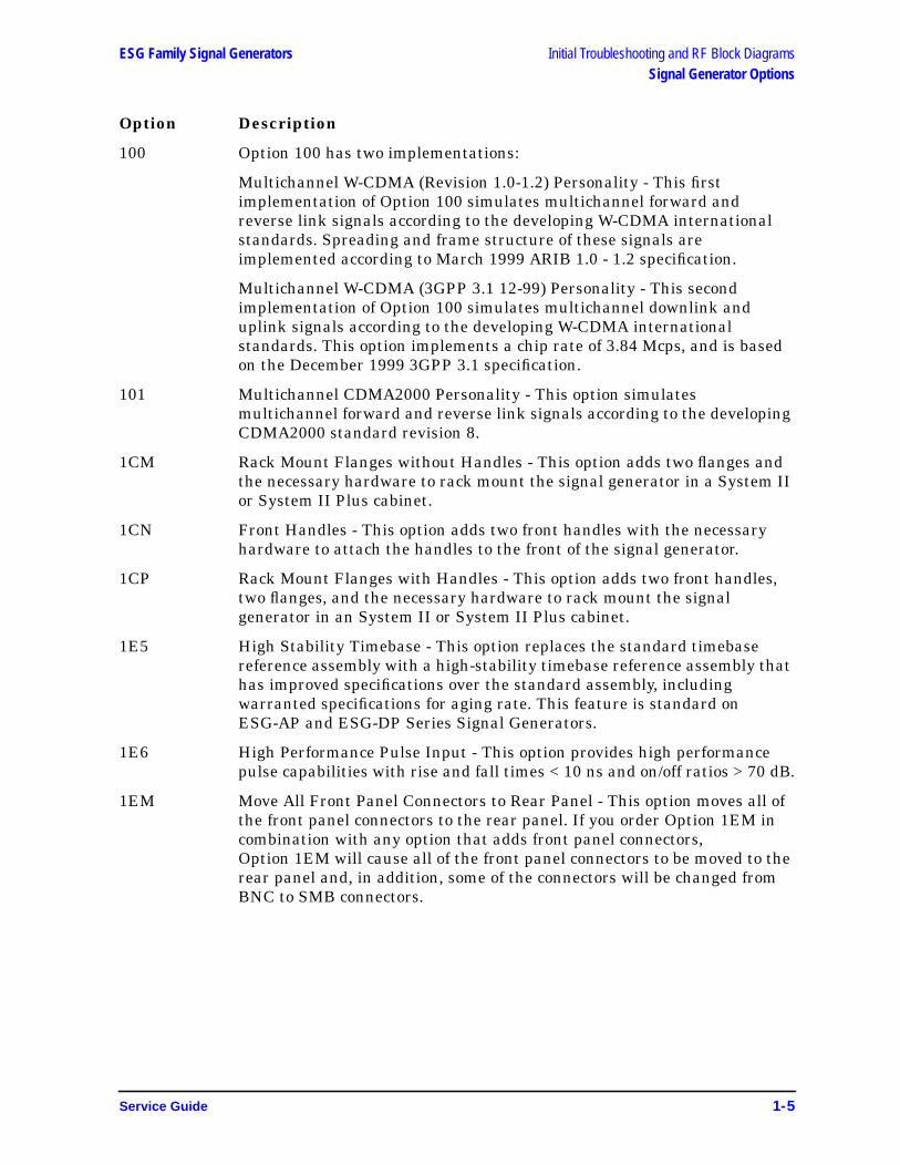
1EM Move All Front Panel Connectors to Rear Panel - This option moves all ofthe front panel connectors to the rear panel. If you order Option 1EM incombination with any option that adds front panel connectors,Option 1EM will cause all of the front panel connectors to be moved to therear panel and, in addition, some of the connectors will be changed fromBNC to SMB connectors.
Service Guide 1-5
Initial Troubleshooting and RF Block Diagrams ESG Family Signal GeneratorsSignal Generator Options
200 Fully Coded 3GPP W-CDMA Personality - This option can be used toprovide fully-coded, multichannel downlink and uplink signals incompliance with 3GPP specifications. Support for this 3GPP W-CDMAsolution may require the use of two ESG signal generators.
201 Multichannel Real-Time cdma2000 Personality - This option can be usedto provide fully-coded, multichannel forward and reverse link signalssupporting both the IS-95 and IS-2000 CDMA standards.
Support for IS-2000 may require the use of two ESG signal generators.Because IS-2000 provides backward compatibility with IS-95 in RC1 andRC2 configurations, the Option 201 personality also supports the IS-95standard.
300 Base Station BERT Extension for Option UN7 - This option adds bit errorrate testing for GSM base stations to the ESG/VSA combination.
ES1 This option indicates that a more recent version of firmware is resident inthe signal generator than was originally shipped. The operating featuresin the new firmware may be different than those documented in youroriginal manual set.
UN3 I/Q Baseband Generator with 1 Mbit Pattern RAM (Obsolete) - This optionis no longer available. Option UN3 provided an I/Q baseband generatorwith DECT, GSM, NADC, PDC, PHS, and TETRA digital modulationformats. Option UN3 is replaced by Option UN8.
UN4 I/Q Baseband Generator with 8 Mbit Pattern RAM (Obsolete) - This optionis no longer available. Option UN4 provided an I/Q baseband generatorwith DECT, GSM, NADC, PDC, PHS, and TETRA digital modulationformats. Pre-modulation filtering selections and PRBS capability wereprovided. Option UN4 is replaced by Option UN8 with Option UN9.
UN5 Multi-Channel CDMA - This option provides multi-channel IS-95 CDMAcapability, which provides flexible, coded-channel setups for CDMA basestations or mobiles, components, or sub-system test.
UN7 Bit Error Rate Test - This option adds a bit error rate test function thatevaluates PN9 or PN15 bit streams for errors. Configuration of data, clock,and clock gate inputs allow testing of demodulated TDMA or CDMAformats. A baseband generator must be part of the instrumentconfiguration.
UN8 Real-time I/Q Baseband Generator - This option provides a custommodulation generator with 1 Mbit of pattern RAM. The custommodulation generator provides generic symbol building, variable symbolrates, and variable filter capabilities in addition to TDMA protocols.
UN9 +7 MBits RAM - This option adds an additional 7 Mbits of pattern RAM toOption UN8 for very long data pattern generation. You must purchaseOption UN8 in conjunction with Option UN9.
UNA Alternate Timeslot Power Level Control - This option provides alternatetimeslot power level control for adjacent timeslots in TDMA applications.
1-6 Service Guide

ESG Family Signal Generators Initial Troubleshooting and RF Block DiagramsSignal Generator Options
UNB High Power with Mechanical Attenuator - This option provides amechanical attenuator that provides 4 to 6 dB more output power than thestandard electronic attenuator.
UND Internal Dual Arbitrary Waveform Generator - This option provides aninternal dual arbitrary waveform generator that contains an on-boarddigital signal processor capable of playing back downloaded waveforms togenerate complex, digitally modulated signals. A 1 Megasample perchannel memory accepts I/Q files from different waveform generationprograms, such as Omnisys and Matlab. 14 bit DACs optimize dynamicrange and reduce noise.
Service Guide 1-7

Initial Troubleshooting and RF Block Diagrams ESG Family Signal GeneratorsContacting Agilent Technologies
Contacting Agilent TechnologiesThis section prepares you for contacting Agilent Technologies should you have a problemwith your signal generator.
Check the Basics before Contacting Agilent TechnologiesOften problems may be solved by repeating what was being done when the problemoccurred. A few minutes spent in performing these simple checks may eliminate timespent waiting for instrument repair.
• Check that the signal generator is plugged into the proper ac power source.
• Check that the line socket has power.
• Check that the signal generator is turned on.
• Check that the other equipment, cables, and connectors are connected properly andoperating correctly.
• Check the equipment settings in the procedure that was being used when the problemoccurred.
• Check that the test being performed and the expected results are within thespecifications and capabilities of the signal generator. (Refer to the calibration guide.)
• Check the signal generator display for error messages. (Refer to the Error Messagesguide.)
• Check operation by performing the verification procedures in the calibration guide.Record all results in the performance test record.
Review the WarrantyIf there is still a problem, read the warranty printed in Chapter 7, “Safety and Regulatory.”If your signal generator is covered by a separate maintenance agreement, be familiar withits terms.
Agilent Technologies offers several maintenance plans to service your signal generatorafter warranty expiration. Call your Agilent Technologies sales and service office for fulldetails.
Calling Agilent Technologies Sales and Service OfficesSales and service offices are located around the world to provide complete support for yoursignal generator. To obtain servicing information, contact the nearest Agilent TechnologiesSales and Service office listed in Table 1-1. For information on ordering parts refer toChapter 3 or Chapter 4.
In any correspondence or telephone conversation, refer to the signal generator by its modelnumber and full serial number. With this information, the Agilent Technologiesrepresentative can quickly determine whether your unit is still within its warranty period.
1-8 Service Guide

ESG Family Signal Generators Initial Troubleshooting and RF Block DiagramsContacting Agilent Technologies
Table 1-1 Agilent Technologies Sales and Service Offices
UNITED STATESInstrument Support CenterAgilent Technologies(800) 403-0801
EUROPEAN FIELD OPERATIONSHeadquartersAgilent Technologies S.A.150, Route du Nant-d’Avril1217 Meyrin 2/ GenevaSwitzerland(41 22) 780.8111
FranceAgilent Technologies France1 Avenue Du CanadaZone D’Activite DeCourtaboeufF-91947 Les Ulis CedexFrance(33 1) 69 82 60 60
GermanyAgilent Technologies GmbHAgilent Technologies Strasse61352 Bad Homburg v.d.HGermany(49 6172) 16-0
Great BritainAgilent TechnologiesEskdale Road, WinnershTriangle Wokingham,Berkshire RG41 5DZEngland(44 118) 9696622INTERCON FIELD OPERATIONSHeadquartersAgilent Technologies3495 Deer Creek Rd.Palo Alto, CA 94304-1316USA(650) 857-5027
JapanAgilent Technologies Japan,Ltd.9-1 Takakura-Cho, HachiojiTokyo 192, Japan(81 426) 60-2111
AustraliaAgilent Technologies AustraliaLtd.31-41 Joseph StreetBlackburn, Victoria 3130(61 3) 895-2895
SingaporeAgilent TechnologiesSingapore (Pte.) Ltd.150 Beach Road#29-00 Gateway WestSingapore 0718(65) 291-9088
CanadaAgilent Technologies(Canada) Ltd.17500 South Service RoadTrans-Canada HighwayKirkland, Quebec H9J 2X8Canada(514) 697-4232
TaiwanAgilent Technologies Taiwan8th Floor, H-P Building337 Fu Hsing North RoadTaipei, Taiwan(886 2) 712-0404
ChinaChina Agilent Technologies38 Bei San Huan X1 RoadShuang Yu ShuHai Dian DistrictBeijing, China(86 1) 256-6888
Service Guide 1-9

Initial Troubleshooting and RF Block Diagrams ESG Family Signal GeneratorsContacting Agilent Technologies
Returning Your Signal Generator for ServiceUse the information in this section if you need to return the signal generator toAgilent Technologies.
Packaging the Signal GeneratorUse the following steps to package the signal generator for shipment to AgilentTechnologies for service:
1. Fill out a blue repair tag (available at the end of this chapter) and attach it to theinstrument. Be as specific as possible about the nature of the problem. Send a copy ofany or all of the following information:
• Any error messages that appeared on the signal generator display.
• A completed performance test record from the calibration guide for your instrument.
• Any other specific data on the performance of the signal generator.
2. Use the original packaging materials or a strong shipping container that is made ofdouble-walled, corrugated cardboard with 159 kg (350 lb) bursting strength. The cartonmust be both large enough and strong enough to accommodate the signal generator andallow at least 3 to 4 inches on all sides of the signal generator for packing material.
CAUTION Signal generator damage can result from using packaging materials otherthan those specified. Never use styrene pellets, in any shape, as packagingmaterials. They do not adequately cushion the instrument or prevent it fromshifting in the carton. Styrene pellets cause equipment damage by generatingstatic electricity and by lodging in the signal generator fan.
3. Surround the instrument with at least 3 to 4 inches of packing material, or enough toprevent the instrument from moving in the carton. If packing foam is not available, thebest alternative is SD-240 Air Cap™ from Sealed Air Corporation (Hayward, CA94545). Air Cap looks like a plastic sheet covered with 1-1/4 inch air-filled bubbles. Usethe pink Air Cap to reduce static electricity. Wrap the instrument several times in thematerial to both protect the instrument and prevent it from moving in the carton.
4. Seal the shipping container securely with strong, nylon adhesive tape.
5. Mark the shipping container “FRAGILE, HANDLE WITH CARE” to ensure carefulhandling.
6. Retain copies of all shipping papers.
1-10 Service Guide

ESG Family Signal Generators Initial Troubleshooting and RF Block DiagramsEquipment Required for Troubleshooting
Equipment Required for TroubleshootingTable 1-2 lists the equipment required to troubleshoot your signal generator. You may usethe recommended model or an equivalent that meets the critical specifications.
Table 1-2 Recommended Test Equipment
Equipment Critical Specifications forEquipment Substitution
RecommendedModel Number
DigitalMultimeter
Input Resistance: ≤10 MΩ Accuracy:10 mV on 100 V range
Agilent 3458A
Service Guide 1-11

Initial Troubleshooting and RF Block Diagrams ESG Family Signal GeneratorsInitial Troubleshooting
Initial TroubleshootingPerform the following troubleshooting steps in the order they are presented. If you areunable to identify the failed assembly, go to Chapter 2, “Assembly-Level Troubleshootingwith Block Diagrams,” for further instruction.
NOTE Do not attempt to replace any fuses within the power supply to correct aproblem with your signal generator. If you determine that the power supply isthe failed assembly, replace the power supply.
Step 1: Observe the Front and Rear Panel LEDsObserving the LEDs on the front and rear panel of the signal generator will determine ifthere is a catastrophic failure in the power supply assembly.
1. Ensure the signal generator is plugged in (do not switch the power on) and verify thatthe yellow LED on both the front and rear panels is lit. Refer to Figure 1-1 for LEDlocations. A lit yellow LED (+15 V_STBY) indicates that line voltage is present.
2. Power on the signal generator and verify that the green LED on both the front and rearpanels is lit. A lit green LED indicates the power supply has received an “ON”command. The ON/OFF switch toggles a flip-flop latch which biases the propertransistors in the LED control circuit. This circuit is powered by VBAT, thebattery-backed SRAM supply, so that the on-off state is “remembered” even when theinstrument is unplugged.
Figure 1-1 LED Locations on the Front and Rear Panels
1-12 Service Guide
ESG Family Signal Generators Initial Troubleshooting and RF Block DiagramsInitial Troubleshooting
Step 2: Power On the Signal Generator and Check for ErrorMessagesThis procedure verifies that the signal generator powers up and that the internalinstrument check identifies no errors. The internal check evaluates the correctness ofoperation and returns an error message if a problem is detected.
1. Switch on the signal generator. Let the signal generator warm up for at least fiveminutes.
NOTE For ESG-AP, ESG-DP, and Option 1E5 signal generators, ERROR 514,Reference Oven Cold will occur whenever the signal generator is poweredup within five minutes of being connected to AC line power. The OVEN COLDannunciator and the ERR annunciator will both turn on. The OVEN COLDannunciator will automatically clear after approximately five minutes. Theerror queue cannot be cleared, however, until the OVEN COLDannunciator hasturned off.
2. Cycle the power to the signal generator and verify that the green LED on both the frontand rear panels is lit. Refer to Figure 1-1.
3. When the display is lit, check to see if the ERR annunciator is turned on.
4. If the ERRannunciator is turned on, review the error messages in the queue by pressingUtility > Error Info > View Next Error Message . The first error message in the queue will beshown in the text area of the display. Refer to the Error Messages guide for descriptionsof error messages.
If there is more than one error message (each message will be designated as 1 of n),continue pressing the View Next Error Message softkey until you have seen and recorded allof the messages.
5. If you were able to resolve all of the error messages, press Utility > Error Info >Clear Error Queue(s) to delete the list of error messages.
Service Guide 1-13
Initial Troubleshooting and RF Block Diagrams ESG Family Signal GeneratorsInitial Troubleshooting
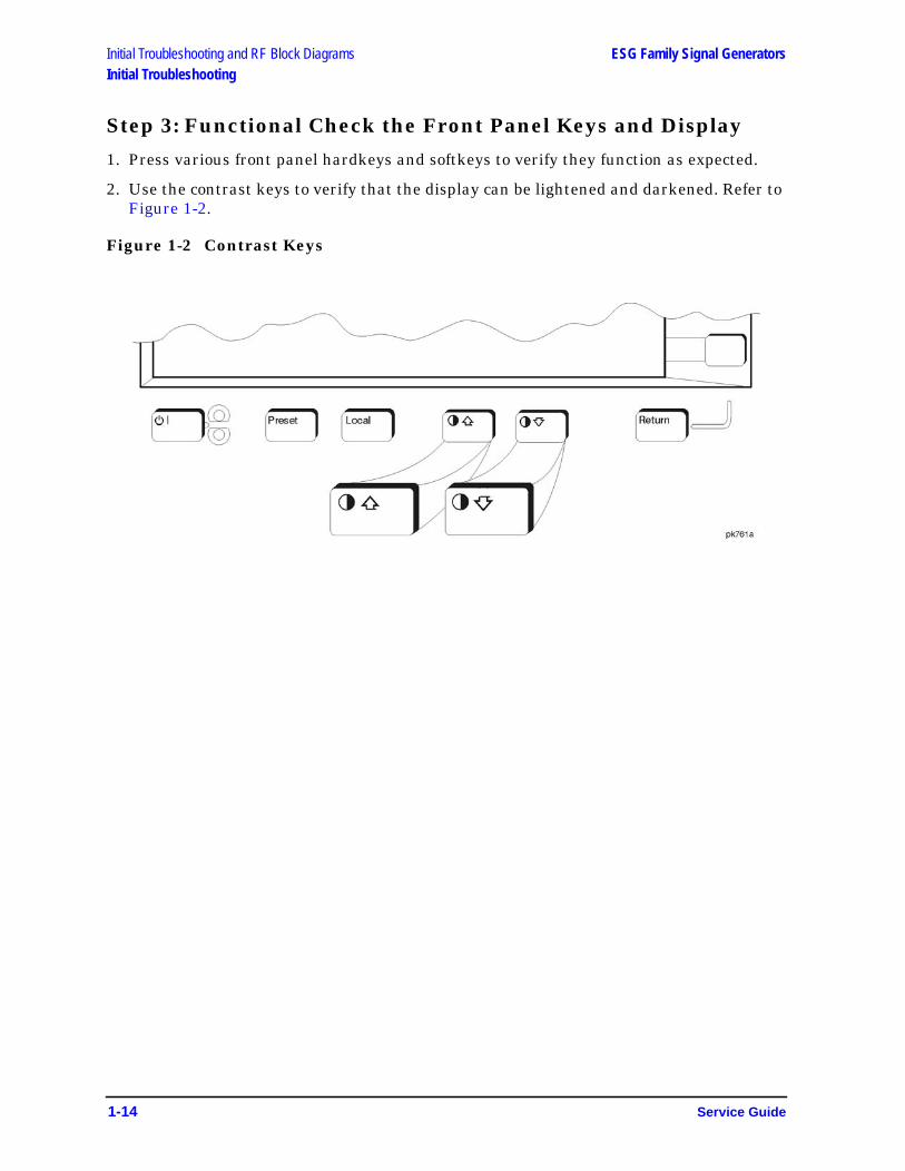
Step 3: Functional Check the Front Panel Keys and Display
1. Press various front panel hardkeys and softkeys to verify they function as expected.
2. Use the contrast keys to verify that the display can be lightened and darkened. Refer toFigure 1-2.
Figure 1-2 Contrast Keys
1-14 Service Guide

ESG Family Signal Generators Initial Troubleshooting and RF Block DiagramsInitial Troubleshooting
Step 4: Visually Check the Individual Voltage Supplies
1. Unplug the signal generator and remove the instrument cover. Refer to Chapter 5,“Assembly Replacement,” for removal instructions.
2. Expose the motherboard by removing the top cover. It is secured by 11 screws.
3. Plug in the signal generator and allow it to warm up for at least five minutes.
4. If possible, clear the error queue(s) of messages. Press Utility > Error Info > Clear ErrorQueue(s) .
5. On the motherboard, locate the 10 LEDs that correspond to the individual voltagesupplies (see Figure 1-3). Verify that all the LEDs are lit. If one or more LEDs are off,proceed to “Step 6: Isolate the Failed Assembly”.
Figure 1-3 LED Locations on the Motherboard
Service Guide 1-15

Initial Troubleshooting and RF Block Diagrams ESG Family Signal GeneratorsInitial Troubleshooting
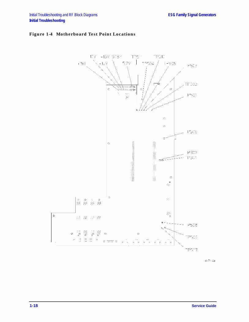
Step 5: Measure the Individual Voltage SuppliesThe voltages supplied as inputs from the power supply via J6 to the motherboard are+15 V (TP502), +15 V standby (+15 V_STBY), −15 V (TP503), +12 V (TP505), and+5.2 V (TP302). DGND (TP301) is associated with these supplies.
The −6 V (TP508) and −5.2 V (TP509) supplies receive their input from the +5.2 V digitalsupply (5.2 VD at TP506). The +5.2 V digital line is filtered to prevent the switching powersupply noise from being induced onto the +5.2 VD supply lines. The −6 V is a bias voltagefor circuits on the output board and other RF circuitry. The −5.2 V is used by the emittercoupled logic (ECL) digital ICs. The LCD display driver voltage (VLCD), a −14 V to −24 Vsource, also receives input from the +5.2 VD supply.
The input to the +32 V supply (TP504) is the +12 V supply. The +32 V supply is used by thesynthesizer/doubler assembly. This supply also includes an LC noise filter.
The +12.5 V regulated supply (TP510) originates from the +15 V input. The −12.5 Vregulated supply (TP511) originates from the −15 V input. These two supplies are used bythe solid-state attenuator and the reverse power protection (RPP). The +10 V reference(TP501) originates from the +15 V input. The +9 V supply (TP507) originates from the+10 V reference and the +12 V supply.
1. Unplug the signal generator and turn it upside-down.
2. Expose the motherboard by removing the bottom cover. It is secured by 15 screws.
3. Plug in the signal generator.
4. Measure the voltage of each supply to verify they are within the tolerances listed inTable 1-3. The voltage supply test point locations are shown in Figure 1-4. If all thevoltages are within tolerance, proceed to “Step 7: Check for Basic CPU Functionality”.
1-16 Service Guide

ESG Family Signal Generators Initial Troubleshooting and RF Block DiagramsInitial Troubleshooting
Table 1-3 Voltage Supply Tolerances
Test Point Supply Voltage Tolerance
J6 (pins 2, 3, 12, 13) +5.2 V +/− 3%
J6 (pin 20) +15 V +/− 3%
J6 (pin 18) −15 V +/− 3%
J6 (pin 19) +12 V +/− 3%
J6 (pin 17) +15 V_STBY +/− 5%
TP301 DGND N/A
TP302 +5.2 V +/− 3%
TP501 +10 V_REF +/− 3%
TP502 +15 V +/− 3%
TP503 −15 V +/− 3%
TP504 +32 V +/− 4%
TP505 +12 V +/− 3%
TP506 +5.2 VD +/− 4%
TP507 +9 V +/− 4%
TP508 −6 V +/− 4%
TP509 −5.2 V +/− 4%
TP510 +12.5 V +/− 4%
TP511 −12.5 V +/− 4%
Service Guide 1-17
Initial Troubleshooting and RF Block Diagrams ESG Family Signal GeneratorsInitial Troubleshooting
Figure 1-4 Motherboard Test Point Locations
1-18 Service Guide

ESG Family Signal Generators Initial Troubleshooting and RF Block DiagramsInitial Troubleshooting
Step 6: Isolate the Failed Assembly
1. Switch off the signal generator.
2. Remove or disconnect an assembly. Below is a suggested order of removal/disconnectionbased upon ease.
For the ESG-A and ESG-D Series:
a. A5 Dual Arbitrary Waveform Generator Board (Option UND)
b. A6 Bit Error Rate Test Board (Option UN7)
c. A7 Baseband Generator Board (Options UN3, UN4, UN8, UN9)
d. A8 Data Generator Board (Options UN3, UN4, UN8, UN9)
e. A21 Demodulator Board (Option 300)
f. Front Panel - disconnect A1W1 ribbon cable
g. A3 Inverter - disconnect A3W1
h. A2 Display - disconnect W10
i. AT1 Electronic Attenuator/RPP - disconnect W13
AT1 Mechanical Attenuator and A19 RPP (Option UNB) - disconnect W13 andA19W1
j. A25 Pulse Modulator (Option 1E6) - disconnect A25W1
k. B1 Fan - disconnect B1W1 (disconnect only temporarily)
l. B2 Fan - disconnect B2W1 (disconnect only temporarily)
m. A9 Output Board
n. A11 Reference Board
o. A12 Synthesizer/Doubler Board
p. A20 YIG Down Convertor Assembly (Option 300) - disconnect W31
NOTE Refer to Chapter 3, “Replaceable Parts (ESG-A and ESG-D Series),” forinformation on locating assemblies. Refer to Chapter 5, “AssemblyReplacement,” for information on removing or disconnecting assemblies.
For the ESG-AP and ESG-DP Series:
a. A5 Dual Arbitrary Waveform Generator Board (Option UND)
b. A6 Bit Error Rate Test Board (Option UN7)
c. A7 Baseband Generator Board (Options UN3, UN4, UN8, UN9)
d. A8 Data Generator Board (Options UN3, UN4, UN8, UN9)
e. Front Panel - disconnect A1W1 ribbon cable
f. A3 Inverter - disconnect A3W1
Service Guide 1-19

Initial Troubleshooting and RF Block Diagrams ESG Family Signal GeneratorsInitial Troubleshooting
g. A2 Display - disconnect W10
h. AT1 Electronic Attenuator/RPP - disconnect W13
AT1 Mechanical Attenuator and A19 RPP (Option UNB) - disconnect W13 andA19W1
i. A25 Pulse Modulator (Option 1E6) - disconnect A25W1
j. B1 Fan - disconnect B1W1 (disconnect only temporarily)
k. B2 Fan - disconnect B2W1 (disconnect only temporarily)
l. A9 Output Board
m. A11 Reference Board
n. A23 Sampler Board
o. A24 Frac-N/Divider Board
p. A22 YIG Driver Assembly - disconnect W35
NOTE Refer to Chapter 4, “Replaceable Parts (ESG-AP and ESG-DP Series),” forinformation on locating assemblies. Refer to Chapter 5, “AssemblyReplacement,” for information on removing or disconnecting assemblies.
3. Switch on the signal generator and check the voltage supply LEDs (see Figure 1-3). Ifthe LEDs are lit, you have likely identified the failed assembly. If one or more LEDs arestill off, switch off the signal generator and replace/reconnect the assembly and repeatthis procedure.
1-20 Service Guide

ESG Family Signal Generators Initial Troubleshooting and RF Block DiagramsInitial Troubleshooting
Step 7: Check for Basic CPU FunctionalityThe Digital Signal Processor (DSP) performs a self-diagnostic test at power up. If the DSPis not working, the CPU reports an error.
If the DSP does not seem to be working and the CPU did not report the error, then checkthe CLK_OUT signal at TP701. It should be a 16 MHz signal. (Refer to Figure 1-5.)
The eight LEDs of DS201 (see Figure 1-5) indicate the status of the boot and flash ROM forthe CPU. The LEDs form a binary code that can be described as a two digit hexadecimalcode. Table 1-4 shows the test sequence and the LED pattern (binary representation) of thetest that is running. If an error occurs and the test is halted, the LED pattern will indicatewhich self test halted the process. The LED closest to R201 is the place holder for the LeastSignificant Bit (LSB) in the pattern.
Table 1-4 Sequence for DSP Self-Diagnostic Tests
Test Description HexadecimalCode
BinaryEquivalentMSB LSB
LEDs at start of test FF 1111 1111
Checksum test FE 1111 1110
Bootrom RAM test FD 1111 1101
RAM test FC 1111 1100
I/O bus test FB 1111 1011
Main firmware checksum test FA 1111 1010
CPU test AA 1010 1010
Test done and OK 00 0000 0000
Service Guide 1-21

Initial Troubleshooting and RF Block Diagrams ESG Family Signal GeneratorsInitial Troubleshooting
Figure 1-5 Location of TP701 and DS201-208 on CPU/Motherboard
1-22 Service Guide

ESG Family Signal Generators Initial Troubleshooting and RF Block DiagramsAdditional Information for Troubleshooting the ESG-AP and ESG-DP Series
Additional Information for Troubleshooting theESG-AP and ESG-DP SeriesTable 1-5 provides frequency-dependent settings for selected points in the RF signal flow ofthe ESG-AP and ESG-DP Series Signal Generators. Notice that the settings are relative tothe RF output frequency. This information can improve your understanding of the signalgenerator circuitry, especially when used with the RF block diagram.
NOTE The values for Table 1-5 assume FM modulation is turned off.
Table 1-5 Frac-N, YO, and Other Selected Frequency-Dependent Settings for SeveralRF Output Frequencies
FreqOut
(MHz)
FreqYO
(MHz)N P Frac-N
(MHz)Fif (MHz) Fs (MHz) Hi/Low Output
Divider
4000 8000 9 8 593.75000 37.1093750 884.7656250 High 2
3000 6000 7 10 644.53125 32.2265625 852.5390625 High 2
2271 4542 7 10 605.62500 30.2812500 644.5312500 Low 2
1500 6000 7 10 644.53125 32.2265625 852.5390625 High 4
1001 4004 5 10 685.46875 34.2734375 793.9453125 High 4
1000 8000 9 8 593.75000 37.1093750 884.7656250 High 8
700 5600 7 10 847.65625 42.3828125 793.9453125 High 8
300 4800 6 10 726.56250 36.3281250 793.9453125 High 16
240 6080 7 10 603.90625 30.1953125 864.2578125 High 8
100 7200 8 9 928.12500 51.5625000 893.5546875 High 8
1 7992 9 8 887.62500 55.4765625 881.8359375 High 8
Service Guide 1-23

BOARD
LIN_AM_MOD
PULSE MOD
ALCMODULATOR
DRIVER
DETECTORSHAPING
DAC
ALCMODULATOR
BURSTMODULATOR
DRIVER
BURSTMODULATOR
.75-1 GHz .0-.25 GHz
.25-4 GHz
ALC REF
ALCHOLD
HOLD ALC
1 GHz REF
50
ALCDETECTOR
IN_BAND_AM
ALC_REF
FE
ED
FO
RW
AR
D A
M
RPP
C ATTENUATOR
/RPP
5dB STEPATTENUATOR
E PULSE MOD
OPTION 1E6
PULSEINPUT
ESG-A SERIES RF BLOCK DIAGRAM
ESG-A SERIES RF BLOCK DIAGRAM
(STANDARD & OPTION 1E6)
RF Out
A SYNTHESIZER BOARD
d/dt
FM
Om/
.5-1 GHz
5 MHz
VARIABLEMODULUS
PRESCALER
FRACTIONALDIVIDE
fF
.25-4 GHz
X2
X2
2
B OUTPUT
LIN_AM_MOD
D REFERENCE BOARDLF OUT
EXT 1INPUT
EXT 2INPUT
EXT REF
FM_MOD
PLL
PLL
NC
10 MHz BW
PULSE MOD
1 GHz PLL
10 MHzSYNTH
1 GHzREF
10 MHzOUT
10 MHz PLL
(STANDARD & OPTION 1E6)
sk766b
2

ESG-D SERIES RF BLOCK DIAGRAM
LIN_AM_MOD
PULSE MOD
s
1 GHz REF
FE
ED
FO
RW
AR
D A
M
ALCMODULATOR
DRIVER
DETECTORSHAPING
DAC
DAC
DAC
ALCMODULATOR
BURSTMODULATOR
DRIVER
TOR
BURSTMODULATOR
.75-1 GHz.75-1 GHz .0-.25 GHz.0-.25 GHz
.25-4 GHz
0
CALVOLTAGE
CALVOLTAGE
Q GAIN
Q OFFSET
ALC REF
ALCHOLD
HOLD ALC
IN_BAND_AM
RPP
50
C ATTENUATOR /RPP
5dB STEPATTENUATOR
ALCDETECTOR
ALC_REF
A SYNTHESIZER BOARD
2
2
d/dt
FM
Om/
.5-1 GHz
5 MHz
VARIABLEMODULUS
PRESCALER
FRACTIONALDIVIDE
X2
X2
fF
LIN_AM_MOD
D REFERENCE BOARD
LF OUT
EXT 1INPUT
EXT 2INPUT
EXT REF
FM_MOD
PLL
PLL
10 MHz BW
PULSE MOD
1 GHz PLL
10 MHzSYNTH
1 GHzREF
10 MHzOUT
10 MHz PLL
B OUTPUT BOARD
10 MHz SYNTH
EXTI INPUT
EXTQ INPUT
DAC
DAC
DAC
DAC
IQ MODULA
90
VBLO
QUAD
.25-4 GHz
AUXOUT
CARRIER)(COHERENT
I GAIN
I OFFSET
k773b ESG-D SERIES RF BLOCK DIAGRAM

ESG-D SERIES RF BLOCK DIAGRAM (OPTIONS UN3 & UN4)
LIN_AM_MOD
PULSE MOD
E
FE
ED
FO
RW
AR
D A
Msk
ALCMODULATOR
DRIVER
DETECTORSHAPING
DAC
DAC
DAC
ALCMODULATOR
BURSTMODULATOR
DRIVER
TOR
BURSTMODULATOR
.75-1 GHz.75-1 GHz .0-.25 GHz.0-.25 GHz
.25-4 GHz
0
CALVOLTAGE
CALVOLTAGE
Q GAIN
Q OFFSET
ALC REF
ALCHOLD
HOLD ALC
IN_BAND_AM
LIN_BURST
LO
G_
BU
RS
T
1 GHz REF
RPP
50
C ATTENUATOR /RPP
5dB STEPATTENUATOR
ALCDETECTOR
BURST_ENVELOPE
1V_REF
ALC_REF
BURSTINT
_ Q
_M
OD
INT_ I_MOD
BURST MODSWITCH & FILTERS
OLDELAY
URST_PLS
BURST_PULSE
A SYNTHESIZER BOARD
2
2
d/dt
FM
Om/
.5-1 GHz
5 MHz
VARIABLEMODULUS
PRESCALER
FRACTIONALDIVIDE
X2
X2
fF
LIN_AM_MOD
D REFERENCE BOARDLF OUT
EXT 1INPUT
EXT 2INPUT
XT REF
FM_MOD
PLL
PLL
10 MHz BW
PULSE MOD
1 GHz PLL
10 MHzSYNTH
1 GHzREF
10 MHzOUT
10 MHz PLL
E BASEBAND GENERATOR BOARD
F DATA GENERATOR BOARD
DATA_CLOCK
10 MHz DIG
EXT 13 MHz
EVENT 1
PATTERNTRIG
EVENT 2
EXTI INPUT
EXTQ INPUT
B OUTPUT BOARD
DAC
DAC
DAC
DAC
IQ MODULA
90
VBLO
QUAD
.25-4 GHz
AUXOUT
CARRIER)(COHERENT
10 MHz SYNTH
I GAIN
I OFFSET
-
DATASWITCH
MASTERCLOCK-PLL
MASTER_CLK
PLL_LCK_SIG
PL
L_
CL
OC
K
L DATA_CLK
BBG_BIT_CLK
SUB_I_COUNT
BUF_DATA_IN
L_BURST
BURST_GATE
USER_DATA
SYMBOL_SYNC
SCRAMBLE_RUN
SYMBOL_SYNC
DATAGENERATION
CONTROL
DAC
DAC
EXT_SYNC
DATA
EXT_BURST
INTERNAL DATAGENERATOR
(PATTERN RAM)UN3=1MUN4=8M
CONTRBURST &
B
774b ESG-D SERIES RF BLOCK DIAGRAM (OPTIONS UN3 & UN4)
ESG-D SERIES RF BLOCK DIAGRAM
LIN_AM_MOD
PULSE_MOD
L
I
EX
FE
ED
FO
RW
AR
D A
M
ALCMODULATORDRIVER
ALCMODULATOR
BURSTMODULATOR
.75-1 GHz .0-.25 GHz
.25-4 GHz
TAGE
Q GAIN
Q OFFSET
LIN_BURST
LO
G_
BU
RS
T
1 GHz REF
50
INT
_ Q
_M
OD
INT_ I_MOD
OD
BURST_ENVELOPE
BURSTMODULATORDRIVER
ALCHOLD
HOLD ALC
ALCDETECTOR
IN_BAND_AM
ALC_REF
BURST
DETECTORSHAPING
DAC
ALC REF
RPP
C ATTENUATOR /RPP
5dB STEPATTENUATOR
DAC
DAC
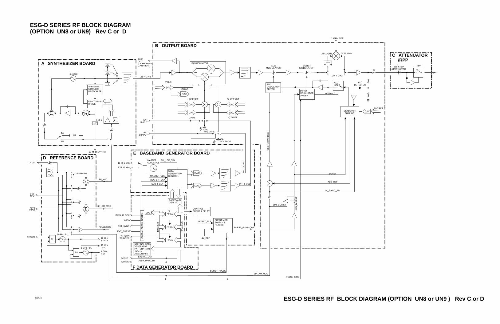
(OPTION UN8 or UN9) Rev C or D
A SYNTHESIZER BOARD
2
2
d/dt
FM
Om/
.5-1 GHz
5 MHz
VARIABLEMODULUSPRESCALER
FRACTIONALDIVIDE
X2
X2
fF
LIN_AM_MOD
D REFERENCE BOARDF OUT
EXT 1INPUT
EXT 2NPUT
T REF
FM_MOD
PLL
PLL
10 MHz BW
PULSE MOD
1 GHz PLL
10 MHzSYNTH
1 GHzREF
10 MHzOUT
10 MHz PLL
E BASEBAND GENERATOR BOARD
F DATA GENERATOR BOARD
10 MHz DIG
EXT 13 MHz
EXTI INPUT
EXTQ INPUT
B OUTPUT BOARD
IQ MODULATOR
090
VBLO
QUAD
.25-4 GHz
10 MHz SYNTH
CALVOLTAGE
CALVOL
I GAIN
I OFFSET
-1V_REF
MASTERCLOCK-PLL
MASTER_CLK
PLL_LCK_SIG
BBG_BIT_CCK
SUB_I_CLK
DATAGENERATIONCONTROL
BURST MSWITCH &FILTERS
CONTROLBURST & DELAY
BURST_PLS
BURST_PULSE
DAC
DAC
DAC
DAC
DAC
DAC
AUXOUT(COHERENTCARRIER)
DATA_CLOCK
EVENT 1
PATTERNTRIGGER
EVENT 2USER_DATA_EN
EVENT1_OUT
DATA
EXT_BURST
EXT_SYNC
GL
OB
AL C
LO
CK
IN
PU
TS
INTERNAL DATAGENERATOR(PATTERN RAM)UN8=1MUN8&UN9=8M
MPUFPGA
FPGA
FPGA
MP
U B
US
FP
GA
BU
S
BASEBANDGEN. I/O
sk77c ESG-D SERIES RF BLOCK DIAGRAM (OPTION UN8 or UN9 ) Rev C or D
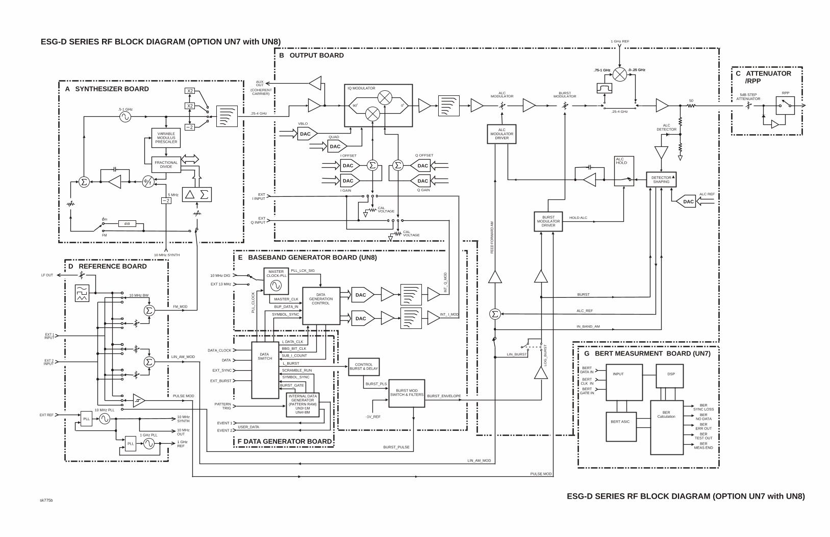
ESG-D SERIES RF BLOCK DIAGRAM (OPTION UN7 with UN8)
LIN_AM_MOD
PULSE MOD
LF OU
EXINP
EXINP
EXT R
FE
ED
FO
RW
AR
D A
M
sk775
)
ALCMODULATOR
DRIVER
DETECTORSHAPING
DAC
DAC
DAC
ALCMODULATOR
BURSTMODULATOR
DRIVER
R
BURSTMODULATOR
.75-1 GHz.75-1 GHz .0-.25 GHz.0-.25 GHz
.25-4 GHz
0
CALVOLTAGE
CALVOLTAGE
Q GAIN
Q OFFSET
ALC REF
ALCHOLD
HOLD ALC
IN_BAND_AM
LIN_BURST
LO
G_B
UR
ST
1 GHz REF
RPP
50
C ATTENUATOR /RPP
5dB STEPATTENUATOR
ALCDETECTOR
BURST_ENVELOPE
REF
ALC_REF
BURST
INT
_ Q
_M
OD
INT_ I_MOD
BURST MODSWITCH & FILTERS
AY
ST_PLS
BURST_PULSE
G BERT MEASURMENT BOARD (UN7)
INPUT
BERTDATA IN
BERTCLK IN
BERTGATE IN
BERT ASIC
BERSYNC LOSS
BERNO DATA
BERERR OUT
BERTEST OUT
BERMEAS END
DSP
BERCalculation
A SYNTHESIZER BOARD
2
2
d/dt
FM
Om/
.5-1 GHz
5 MHz
VARIABLEMODULUS
PRESCALER
FRACTIONALDIVIDE
X2
X2
fF
LIN_AM_MOD
D REFERENCE BOARDT
T 1UT
T 2UT
EF
FM_MOD
PLL
PLL
10 MHz BW
PULSE MOD
1 GHz PLL
10 MHzSYNTH
1 GHzREF
10 MHzOUT
10 MHz PLL
E BASEBAND GENERATOR BOARD (UN8
F DATA GENERATOR BOARD
DATA_CLOCK
10 MHz DIG
EXT 13 MHz
EVENT 1
PATTERNTRIG
EVENT 2
EXTI INPUT
EXTQ INPUT
B OUTPUT BOARD
DAC
DAC
DAC
DAC
IQ MODULATO
90
VBLO
QUAD
.25-4 GHz
AUXOUT
CARRIER)(COHERENT
10 MHz SYNTH
I GAIN
I OFFSET
-1V_
DATASWITCH
MASTERCLOCK-PLL
MASTER_CLK
PLL_LCK_SIG
PL
L_
CL
OC
K
L DATA_CLK
BBG_BIT_CLK
SUB_I_COUNT
BUF_DATA_IN
L_BURST
BURST_GATE
USER_DATA
SYMBOL_SYNC
SCRAMBLE_RUN
SYMBOL_SYNC
DATAGENERATION
CONTROL
DAC
DAC
EXT_SYNC
DATA
EXT_BURST
INTERNAL DATAGENERATOR
(PATTERN RAM)UN3=1MUN4=8M
CONTROLBURST & DEL
BUR
bESG-D SERIES RF BLOCK DIAGRAM (OPTION UN7 with UN8)
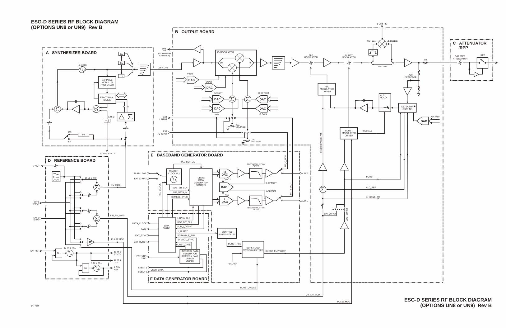
ESG-D SERIES RF BLOCK DIAGRAM (OPTIONS UN8 or UN9) Rev B
ESG-D SERIES RF BLOCK DIAGRAM
DETECTORSHAPING
DAC
DAC
DAC
ALCMODULATOR
ATOR
BURSTMODULATOR
.75-1 GHz.75-1 GHz .0-.25 GHz.0-.25 GHz
.25-4 GHz
0
CALVOLTAGE
CALVOLTAGE
Q GAIN
Q OFFSET
ALC REF
ALCHOLD
1 GHz REF
RPP
50
C ATTENUATOR /RPP
5dB STEPATTENUATOR
ALCDETECTOR
DJ
Q-OFFSET
I-OFFSET
J
INT
_ Q
_M
OD
INT
_ I_M
OD
BURST_PULSE
BURSTMODULATOR
DRIVER
HOLD ALC
IN_BAND_AM
LIN_BURST
LO
G_B
UR
ST
ALC_REF
BURST
BURST_ENVELOPE
-1V_REF
BURST MODSWITCH & FILTERS
ROL DELAY
BURST_PLS
LIN_AM_MOD
FE
ED
FO
RW
AR
D A
M
ALCMODULATOR
DRIVER
AUD 1
AUD 2
RECONSTRUCTIONFILTER
RECONSTRUCTIONFILTER
A SYNTHESIZER BOARD
2
2
d/dt
FM
Om/
.5-1 GHz
5 MHz
VARIABLEMODULUS
PRESCALER
FRACTIONALDIVIDE
X2
X2
fF
LIN_AM_MOD
D REFERENCE BOARDLF OUT
EXT 1INPUT
EXT 2INPUT
EXT REF
FM_MOD
PLL
PLL
10 MHz BW
PULSE MOD
1 GHz PLL
10 MHzSYNTH
1 GHzREF
10 MHzOUT
10 MHz PLL
E BASEBAND GENERATOR BOARD
F DATA GENERATOR BOARD
EXTI INPUT
EXTQ INPUT
B OUTPUT BOARD
DAC
DAC
DAC
DAC
IQ MODUL
90
VBLO
QUAD
.25-4 GHz
AUXOUT
CARRIER)(COHERENT
10 MHz SYNTH
I GAIN
I OFFSET
PLL_LCK_SIG
Q-A
I-AD
DBMICDATA
GENERATIONCONTROL
QDAC
DAC
IDAC
DATA_CLOCK
EVENT 1
PATTERNTRIG
EVENT 2
DATASWITCH
L DATA_CLK
BBG_BIT_CLK
SUB_I_COUNT
L_BURST
BURST_GATE
USER_DATA
SYMBOL_SYNC
SCRAMBLE_RUN
DATA
EXT_SYNC
EXT_BURST
INTERNAL DATAGENERATOR
(PATTERN RAM)UN8=1MUN9=8M
CONTBURST &
10 MHz DIG
EXT 13 MHz
MASTERCLOCK-PLL
MASTER_CLK
PL
L_
CL
OC
K
BUF_DATA_IN
SYMBOL_SYNC
sk776b (OPTIONS UN8 or UN9) Rev BPULSE MOD
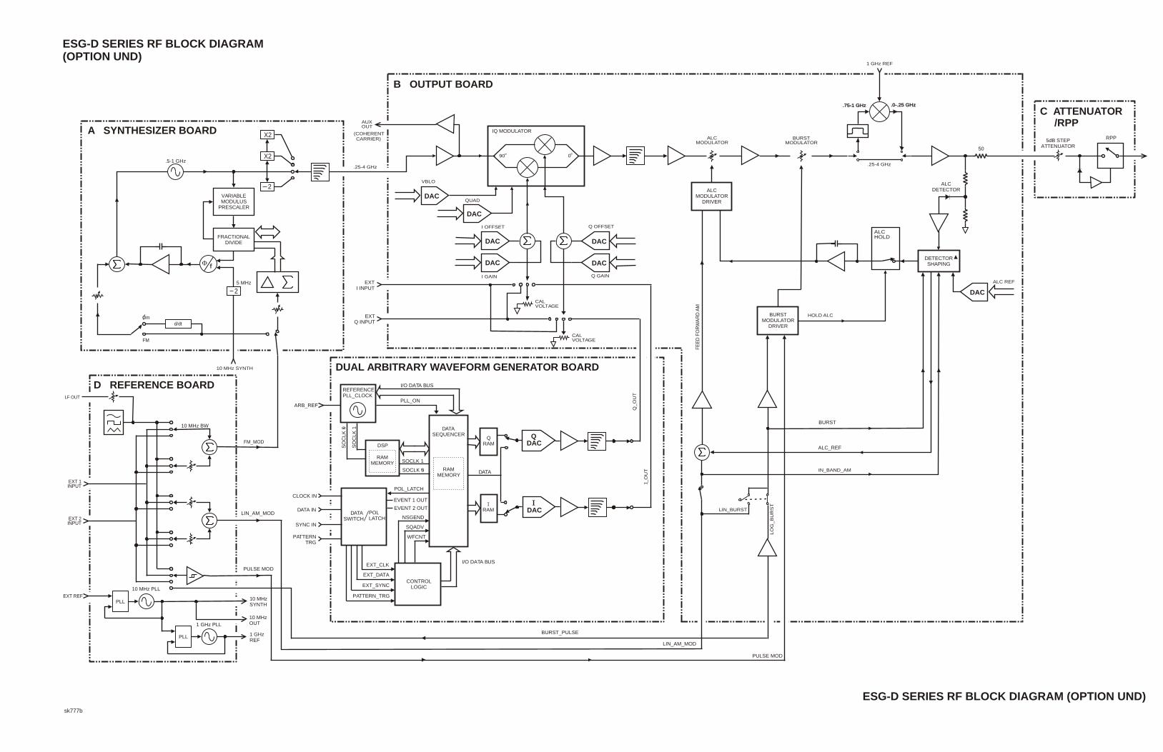
ESG-D SERIES RF BLOCK DIAGRAM (OPTION UND)
LIN_AM_MOD
PULSE MOD
LF
I
I
EX
FE
ED
FO
RW
AR
D A
M
sk
RATOR BOARD
ALCMODULATOR
DRIVER
DETECTORSHAPING
DAC
DAC
DAC
ALCMODULATOR
BURSTMODULATOR
DRIVER
OR
BURSTMODULATOR
.75-1 GHz.75-1 GHz .0-.25 GHz.0-.25 GHz
.25-4 GHz
0
CALVOLTAGE
CALVOLTAGE
Q_
OU
T
Q GAIN
Q OFFSET
ALC REF
ALCHOLD
HOLD ALC
IN_BAND_AM
LIN_BURST
LO
G_
BU
RS
T
1 GHz REF
RPP
50
C ATTENUATOR /RPP
5dB STEPATTENUATOR
ALCDETECTOR
ALC_REF
BURST
DACQ
DAC
BURST_PULSE
I_O
UT
I
A SYNTHESIZER BOARD
2
2
d/dt
FM
Om/
.5-1 GHz
5 MHz
VARIABLEMODULUS
PRESCALER
FRACTIONALDIVIDE
X2
X2
fF
LIN_AM_MOD
D REFERENCE BOARD OUT
EXT 1NPUT
EXT 2NPUT
T REF
FM_MOD
PLL
PLL
10 MHz BW
PULSE MOD
1 GHz PLL
10 MHzSYNTH
1 GHzREF
10 MHzOUT
10 MHz PLL
DUAL ARBITRARY WAVEFORM GENE
CLOCK IN
ARB_REF
EXTI INPUT
EXTQ INPUT
B OUTPUT BOARD
DAC
DAC
DAC
DAC
IQ MODULAT
90
VBLO
QUAD
.25-4 GHz
AUXOUT
CARRIER)(COHERENT
10 MHz SYNTH
I GAIN
I OFFSET
DATA POLLATCH
I/O DATA BUS
SWITCH
REFERENCEPLL_CLOCK
SO
CLK
1
SOCLK 1
POL_LATCH
EVENT 1 OUT
EVENT 2 OUT
NSGEND
SQADV
WFCNT
PLL_ON
I/O DATA BUS
Q RAM
DATA
IRAM
EXT_CLK
EXT_SYNC
PATTERN_TRG
EXT_DATA
DSP
RAMMEMORY
RAMMEMORY
DATASEQUENCER
SYNC IN
DATA IN
PATTERNTRG
CONTROL LOGIC
SO
CL
K 0
SOCLK 0
777b
ESG-D SERIES RF BLOCK DIAGRAM (OPTION UND)

ESG-D SERIES RF BLOCK DIAGRAM
LIN_AM_MOD
PULSE_MOD
L
I
EX
FE
ED
FO
RW
AR
D A
M
ALCMODULATORDRIVER
ALCMODULATOR
BURSTMODULATOR
.75-1 GHz .0-.25 GHz
.25-4 GHz
TAGE
Q GAIN
Q OFFSET
LIN_BURST
LO
G_
BU
RS
T
1 GHz REF
50
INT
_ Q
_M
OD
INT_ I_MOD
OD
BURST_ENVELOPE
BURSTMODULATORDRIVER
ALCHOLD
HOLD ALC
ALCDETECTOR
IN_BAND_AM
ALC_REF
BURST
DETECTORSHAPING
DAC
ALC REF
G BERT MEASURMENT BOARD
INPUTBERT
DATA IN
BERT
CLK IN
BERT
GATE IN
BERT ASIC
BERSYNC LOSS
BERNO DATA
BERERR OUT
BERTEST OUT
BERMEAS END
DSP
BERCALCULATION
RPP
C ATTENUATOR /RPP
5dB STEPATTENUATOR
DAC
DAC
OPTION 300
DEMODULATOR
DAC
IFADC
FPGA
CLK
CLK
DSP
INTERFACE SWITCH
DOWN CONVERTER
FPGA
MEMORY
PLL
26 MHz REF
12
CLOCKDATA
GAIN
fF
321.4MHz
(OPTION UN7, UN8/UN9, 300)
A SYNTHESIZER BOARD
2
2
d/dt
FM
Om/
.5-1 GHz
5 MHz
VARIABLEMODULUSPRESCALER
FRACTIONALDIVIDE
X2
X2
fF
LIN_AM_MOD
D REFERENCE BOARDF OUT
EXT 1INPUT
EXT 2NPUT
T REF
FM_MOD
PLL
PLL
10 MHz BW
PULSE MOD
1 GHz PLL
10 MHzSYNTH
1 GHzREF
10 MHzOUT
10 MHz PLL
E BASEBAND GENERATOR BOARD
F DATA GENERATOR BOARD
10 MHz DIG
EXT 13 MHz
EXTI INPUT
EXTQ INPUT
B OUTPUT BOARD
IQ MODULATOR
090
VBLO
QUAD
.25-4 GHz
10 MHz SYNTH
CALVOLTAGE
CALVOL
I GAIN
I OFFSET
-1V_REF
MASTERCLOCK-PLL
MASTER_CLK
PLL_LCK_SIG
BBG_BIT_CCK
SUB_I_CLK
DATAGENERATIONCONTROL
BURST MSWITCH &FILTERS
CONTROLBURST & DELAY
BURST_PLS
BURST_PULSE
DAC
DAC
DAC
DAC
DAC
DAC
AUXOUT(COHERENTCARRIER)
DATA_CLOCK
EVENT 1
PATTERNTRIGGER
EVENT 2USER_DATA_EN
EVENT1_OUT
DATA
EXT_BURST
EXT_SYNC
GL
OB
AL C
LO
CK
IN
PU
TS
INTERNAL DATAGENERATOR(PATTERN RAM)UN8=1MUN8&UN9=8M
MPUFPGA
FPGA
FPGA
MP
U B
US
FP
GA
BU
S
BASEBANDGEN. I/O
sk7110b ESG-D SERIES RF BLOCK DIAGRAM (OPTION UN7, UN8/UN9, 300 )

RPP
H ATTENUATOR /RPP
5dB STEPATTENUATOR
RF OUTPUT
G PULSE MOD
PULSEINPUT
F OUTPUT
AUXOUT
(CoherentCarrier)
EXTI INPUT
EXTQ INPUT
LIN_AM_MOD
FE
ED
FO
RW
AR
D A
M
PULSE MOD
DETECTORSHAPING
BURSTMODULATOR
DRIVER
ALCMODULATOR
DRIVER
ALCMODULATOR
BURSTMODULATOR
HOLD ALC
IN_BAND_AM
ALC_REF
DAC
ALC REF
ALCHOLD
50
ALCDETECTOR
1 GHz REF
.75-1 GHz .0-.25 GHz
.25-4 GHz
DAC
QUAD
DAC
VBLO
DAC
DAC
CALVOLTAGE
CALVOLTAGE
DAC
DAC
I OFFSET
I GAIN Q GAIN
Q OFFSET
090
IQ MODULATOR
2
E DIVIDER (PART OF FRAC-N DIVIDER)
22 2
2-4 GHz
1-2 GHz
.5-1 GHz
.25-.5 GHz
.25-4 GHz
MPLER
F¦
F¦
S+ / -
4
750 MHz
P = 8, 9, or 10
fif
fs
fyo
30-70 MHz
750 MHz
600-735 MHz765-900 MHz
2.93 MHz Steps
6
M 4 < M < 51- -
5 < N < 9- -
f = N * f + fyo s if
2 P
LO
IF
J3RF
256M
PROGRAMMABLEDIVIDER
DATA
cw
fm
cw
fm
750 MHz
RF OUT TOFRAC-N/DIVIDER
DRIVER
J7
J8
RF OUT TOSAMPLER
P/OJ1
-15VTUNEAC
SCALING
OSSER
FMCOIL
MAINCOIL
P/OJ1
YO
<115 Hz
4-8 GHz
ESG-AP SERIES RF BLOCK DIAGRAM (STANDARD &1E6)
D REFERENCE
LIN_AM_MOD
EXT 1INPUT
EXT 2INPUT
10 MHz BW
LF OUT
PULSE MOD
EXT 10 MHzINPUT
VCO1 GHz
1 GHZREF
1 GHz
100PLL
10 MHz
10 MHzSYNTH
10 MHzOUT
10 MHzCLK
PLL
J3
C SA
J6
J11 GHz In
FRAC-N
B YO
FM
PRED
CROV
J4
J3
400-1000 MHz
10 MHz Paren/TesseraFrac-NSYNTH
A FRAC-N (PART OF FRAC-N/DIVIDER)
FM
_M
OD
sk781b ESG-AP SERIES RF BLOCK DIAGRAM (STANDARD & 1E6)

sk767b
RPP
G ATTENUATOR /RPP
5dB STEPATTENUATOR
RF OUTPUT
F OUTPUT
AUXOUT
(CoherentCarrier)
EXTI INPUT
EXTQ INPUT
LIN_AM_MOD
FE
ED
FO
RW
AR
D A
M
PULSE MOD
DETECTORSHAPING
BURSTMODULATOR
DRIVER
ALCMODULATOR
DRIVER
ALCMODULATOR
BURSTMODULATOR
HOLD ALC
IN_BAND_AM
ALC_REF
DAC
ALC REF
ALCHOLD
50
ALCDETECTOR
1 GHz REF
.75-1 GHz .0-.25 GHz
.25-4 GHz
DAC
QUAD
DAC
VBLO
DAC
DAC
CALVOLTAGE
CALVOLTAGE
DAC
DAC
I OFFSET
I GAIN Q GAIN
Q OFFSET
090
IQ MODULATOR
2
E DIVIDER (PART OF FRAC-N DIVIDER)
22 2
2-4 GHz
1-2 GHz
.5-1 GHz
.25-.5 GHz
.25-4 GHz
E
F¦
F¦
S+ / -
P = 8, 9, or 10
fif
fs
fyo
30-70 MHz
750 MHz
600-735 MHz765-900 MHz
2.93 MHz Steps
-
5 < N < 9- -
f = N * f + fyo s if
2 P
LO
IF
J3RF
cw
fm
cw
fm
RF OUT TOFRAC-N/DIVIDER
J7
J8
RF OUT TOSAMPLER
MOIL
INIL
4-8 GHz
ESG-DP SERIES RF BLOCK DIAGRAM
D REFERENCE
LIN_AM_MOD
EXT 1INPUT
EXT 2INPUT
10 MHz BW
LF OUT
PULSE MOD
XT 10 MHzINPUT
VCO1 GHz
1 GHZREF
1 GHz
100PLL
10 MHz
10 MHzSYNTH
10 MHzOUT
10 MHzCLK
PLL
J3
C SAMPLER
4
750 MHz
J6
6
M
J11 GHz In
4 < M < 51-
FRAC-N
256M
PROGRAMMABLEDIVIDER
DATA
750 MHz
B YO DRIVER
P/OJ1
-15V
FM
PRETUNEDAC
SCALING
CROSSOVER
FC
MACO
P/OJ1
YO
J4
J3
<115 Hz
400-1000 MHz
10 MHz Paren/TesseraFrac-NSYNTH
A FRAC-N (PART OF FRAC-N/DIVIDER)
FM
_M
OD
ESG-DP SERIES RF BLOCK DIAGRAM

K BERT MEASURMENT BOARD
INPUT
BERTDATA IN
BERTCLK IN
BERTGATE IN
BERT ASIC
BERSYNC LOSS
BERNO DATA
BERERR OUT
BERTEST OUT
BERMEAS END
DSP
BERCalculation
DAC
DAC
H BASEBAND GENERATOR BOARD
J DATA GENERATOR BOARD
DATA_CLOCK
10 MHz DIG
EXT 13 MHz
EVENT 1
PATTERNTRIG
EVENT 2
BURST_ENVELOPE
-1V_REF
INT
_ Q
_M
OD
DATASWITCH
INT_ I_MOD
MASTERCLOCK-PLL
MASTER_CLK
PLL_LCK_SIG
PL
L_
CL
OC
K
L DATA_CLK
BBG_BIT_CLK
SUB_I_COUNT
BUF_DATA_IN
L_BURST
BURST_GATE
USER_DATA
SYMBOL_SYNC
SCRAMBLE_RUN
SYMBOL_SYNC
DATAGENERATION
CONTROL
BURST MODSWITCH & FILTERS
EXT_SYNC
DATA
EXT_BURST
INTERNAL DATAGENERATOR
(PATTERN RAM)UN3=1MUN4=8M
CONTROLBURST & DELAY
BURST_PLS
ESG-DP SERIES RF BLOCK DIAGRAM (OPTION UN7)
LIN_AM_MOD
RPP
G ATTENUATOR /RPP
5dB STEPATTENUATOR
RF OUTPUT
F OUTPUT
AUXOUT
(CoherentCarrier)
EXTI INPUT
EXTQ INPUT
FE
ED
FO
RW
AR
D A
M
PULSE MOD
DETECTORSHAPING
BURSTMODULATOR
DRIVER
ALCMODULATOR
DRIVER
ALCMODULATOR
BURSTMODULATOR
HOLD ALC
IN_BAND_AM
ALC_REF
DAC
ALC REF
ALCHOLD
50
ALCDETECTOR
1 GHz REF
.75-1 GHz .0-.25 GHz
.25-4 GHz
DAC
QUAD
DAC
VBLO
DAC
DAC
CALVOLTAGE
CALVOLTAGE
DAC
DAC
I OFFSET
I GAIN Q GAIN
Q OFFSET
090
IQ MODULATOR
2
E DIVIDER (PART OF FRAC-N DIVIDER)
22 2
2-4 GHz
1-2 GHz
.5-1 GHz
.25-.5 GHz
.25-4 GHz
C SAMPLER
F¦
F¦
S+ / -
4
750 MHz
J6
P = 8, 9, or 10
fif
fs
fyo
30-70 MHz
750 MHz
600-735 MHz765-900 MHz
2.93 MHz Steps
6
M
J1z In
4 < M < 51- -
5 < N < 9- -
f = N * f + fyo s if
2 P
LO
IF
J3RF
C-N
256M
PROGRAMMABLEDIVIDER
DATA
cw
fm
cw
fm
750 MHz
RF OUT TOFRAC-N/DIVIDER
B YO DRIVER
J7
J8
RF OUT TOSAMPLER
P/OJ1
-15V
FM
PRETUNEDAC
SCALING
CROSSOVER
FMCOIL
MAINCOIL
P/OJ1
YO
4
3
<115 Hz
4-8 GHz
D REFERENCE
LIN_AM_MOD
EXT 1INPUT
EXT 2INPUT
10 MHz BW
LF OUT
PULSE MOD
EXT 10 MHzINPUT
VCO1 GHz
1 GHz
100PLL
10 MHz10 MHz SYNTH
10 MHz OUT
10 MHz CLK
PLL
J3
1 GH
FRA
J
J
400-1000 MHz
10 MHz Paren/TesseraFrac-NSYNTH
A FRAC-N (PART OF FRAC-N/DIVIDER)
FM
_M
OD
1 GHZ REF
BURST_PULSE
sk782b ESG-DP SERIES RF BLOCK DIAGRAM (OPTION UN7)BURST_PULSE

ESG-DP SERIES RF BLOCK DIAGRAM (OPTIONS UN8 or UN9)
LIN_AM_MOD
RPP
G ATTENUATOR /RPP
5dB STEPATTENUATOR
RF OUTPUT
F OUTPUT
AUXOUT
(CoherentCarrier)
EXTI INPUT
EXTQ INPUT
FE
ED
FO
RW
AR
D A
M
PULSE MOD
DETECTORSHAPING
BURSTMODULATOR
DRIVER
ALCMODULATOR
DRIVER
ALCMODULATOR
BURSTMODULATOR
HOLD ALC
IN_BAND_AM
ALC_REF
DAC
ALC REF
ALCHOLD
50
ALCDETECTOR
1 GHz REF
.75-1 GHz .0-.25 GHz
.25-4 GHz
DAC
QUAD
DAC
VBLO
DAC
DAC
CALVOLTAGE
CALVOLTAGE
DAC
DAC
I OFFSET
I GAIN Q GAIN
Q OFFSET
090
IQ MODULATOR
2
E DIVIDER (PART OF FRAC-N DIVIDER)
22 2
2-4 GHz
1-2 GHz
.5-1 GHz
.25-.5 GHz
.25-4 GHz
EF
YNTH
UT
LK
C SAMPLER
F¦
F¦
S+ / -
4
750 MHz
J6
P = 8, 9, or 10
fif
fs
fyo
30-70 MHz
750 MHz
600-735 MHz765-900 MHz
2.93 MHz Steps
6
M
J11 GHz In
4 < M < 51- -
5 < N < 9- -
f = N * f + fyo s if
2 P
LO
IF
J3RF
FRAC-N
256M
PROGRAMMABLEDIVIDER
DATA
cw
fm
cw
fm
750 MHz
RF OUT TOFRAC-N/DIVIDER
B YO DRIVER
J7
J8
RF OUT TOSAMPLER
P/OJ1
-15V
FM
PRETUNEDAC
SCALING
CROSSOVER
FMCOIL
MAINCOIL
P/OJ1
YO
J4
J3
<115 Hz
4-8 GHz
H BASEBAND GENERATOR BOARD
J DATA GENERATOR BOARD
10 MHz DIG
EXT 13 MHz
-1V_REF
INT
_ Q
_M
OD
INT_ I_MOD
MASTERCLOCK-PLL
MASTER_CLK
PLL_LCK_SIG
BBG_BIT_CCK
SUB_I_CLK
DATAGENERATIONCONTROL
BURST MODSWITCH &FILTERS
CONTROLBURST & DELAY
BURST_PLSBURST_PULSE
DAC
DAC
DATA_CLOCK
EVENT 1
PATTERNTRIGGER
EVENT 2USER_DATA_EN
EVENT1_OUT
DATA
EXT_BURST
EXT_SYNC
GL
OB
AL C
LO
CK
IN
PU
TS
INTERNAL DATAGENERATOR(PATTERN RAM)UN8=1MUN8&UN9=8M
MPUFPGA
FPGA
FPGA
MP
U B
US
FP
GA
BU
S
BASEBANDGEN. I/O
BURST_PULSE
D REFERENCE
LIN_AM_MOD
EXT 1INPUT
EXT 2INPUT
10 MHz BW
LF OUT
PULSE MOD
EXT 10 MHzINPUT
VCO1 GHz
1 GHZ R
1 GHz
100PLL
10 MHz10 MHz S
10 MHz O
10 MHz C
PLL
J3
400-1000 MHz
10 MHz Paren/TesseraFrac-NSYNTH
A FRAC-N (PART OF FRAC-N/DIVIDER)
FM
_M
OD
BURST_PULSE
sk783b ESG-DP SERIES RF BLOCK DIAGRAM (OPTIONS UN8 or UN9)

ESG-DP SERIES RF BLOCK DIAGRAM (OPTION UND)
H DUAL ARBITRARY WAVEFORM GENERATOR BOARD
CLOCK IN
ARB_REF
Q_
OU
T
DATA POLLATCH
I/O DATA BUS
SWITCH
REFERENCEPLL_CLOCK
SO
CLK
1
SOCLK 1
POL_LATCH
EVENT 1 OUT
EVENT 2 OUT
NSGEND
SQADV
WFCNT
PLL_ON
I/O DATA BUS
Q RAM
DATA
IRAM
EXT_CLK
EXT_SYNC
PATTERN_TRG
EXT_DATA
DSP
RAMMEMORY
RAMMEMORY
DATASEQUENCER
Q
SYNC IN
DATA IN
PATTERNTRG
CONTROL LOGIC
SO
CL
K 0
SOCLK 0
I_O
UT
I
LIN_AM_MOD
RPP
G ATTENUATOR /RPP
5dB STEPATTENUATOR
RF OUTPUT
F OUTPUT
AUXOUT
(CoherentCarrier)
EXTI INPUT
EXTQ INPUT
FE
ED
FO
RW
AR
D A
M
PULSE MOD
DETECTORSHAPING
BURSTMODULATOR
DRIVER
ALCMODULATOR
DRIVER
ALCMODULATOR
BURSTMODULATOR
HOLD ALC
IN_BAND_AM
ALC_REF
DAC
ALC REF
ALCHOLD
50
ALCDETECTOR
1 GHz REF
.75-1 GHz .0-.25 GHz
.25-4 GHz
DAC
QUAD
DAC
VBLO
DAC
DAC
CALVOLTAGE
CALVOLTAGE
DAC
DAC
I OFFSET
I GAIN Q GAIN
Q OFFSET
090
IQ MODULATOR
2
E DIVIDER (PART OF FRAC-N DIVIDER)
22 2
2-4 GHz
1-2 GHz
.5-1 GHz
.25-.5 GHz
.25-4 GHz
C SAMPLER
F¦
F¦
S+ / -
4
750 MHz
J6
P = 8, 9, or 10
fif
fs
fyo
30-70 MHz
750 MHz
600-735 MHz765-900 MHz
2.93 MHz Steps
6
M
J11 GHz In
4 < M < 51- -
5 < N < 9- -
f = N * f + fyo s if
2 P
LO
IF
J3RF
FRAC-N
256M
PROGRAMMABLEDIVIDER
DATA
cw
fm
cw
fm
750 MHz
RF OUT TOFRAC-N/DIVIDER
B YO DRIVER
J7
J8
RF OUT TOSAMPLER
P/OJ1
-15V
FM
PRETUNEDAC
SCALING
CROSSOVER
FMCOIL
MAINCOIL
P/OJ1
YO
J4
J3
<115 Hz
4-8 GHz
DAC
DAC
LIN_BURST
LO
G_
BU
RS
T
D REFERENCE
LIN_AM_MOD
EXT 1INPUT
EXT 2INPUT
10 MHz BW
LF OUT
PULSE MOD
EXT 10 MHzINPUT
VCO1 GHz
1 GHZREF
1 GHz
100PLL
10 MHz
10 MHzSYNTH
10 MHzOUT
10 MHzCLK
PLL
J3
400-1000 MHz
10 MHz Paren/TesseraFrac-NSYNTH
A FRAC-N (PART OF FRAC-N/DIVIDER)
FM
_M
OD
BURST_PULSE
sk784b ESG-DP SERIES RF BLOCK DIAGRAM (OPTION UND)BURST_PULSE

ESG Family Signal Generators
2 Assembly-Level Troubleshooting withBlock Diagrams
This chapter provides the block diagrams and information necessary for you to test andtroubleshoot the major assemblies of your signal generator.
Service Guide 2-1

Assembly-Level Troubleshooting with Block Diagrams ESG Family Signal GeneratorsBefore You Begin Troubleshooting
Before You Begin TroubleshootingBe sure to review the warning and caution statements described in Chapter 7 prior totroubleshooting your signal generator.
Using this Chapter with Service SoftwareSome block diagrams in this chapter are accompanied by a table for use with theautomated service software that came with your signal generator. These tables list thesignal generator’s test conditions and the expected ABUS node voltages. The servicesoftware has a utility program which measures and displays the node voltages for eachtest. Refer to your signal generator’s calibration guide for information on using thesoftware.
The block diagrams and ABUS node tables are arranged in the following order:
A5 Dual Arbitrary Waveform Generator Block Diagram (Option UND)
A6 Bit Error Rate Test Block Diagram (Option UN7)
A7 Baseband Generator Block Diagram (Options UN3 & UN4)
A7 DBMIC Baseband Generator Block Diagram (Options UN8 & UN9)
A8 Data Generator Block Diagram (Options UN3 & UN4)
A8 Data Generator - Rev. A & B Block Diagram (Options UN8 & UN9)
A8 Flex Data Generator - Rev. C & D Block Diagram (Options UN8 & UN9)
A9 Output ABUS Nodes (ESG-A Series)
A9 Output Block Diagram (ESG-A Series)
A9 Output ABUS Nodes (ESG-D Series)
A9 Output ABUS Nodes (ESG-AP, & ESG-DP Series)
A9 Output Block Diagram (ESG-D, ESG-AP, & ESG-DP Series)
A11 Reference ABUS Nodes (ESG-A & ESG-D Series)
A11 Reference Block Diagram (ESG-A & ESG-D Series)
A11 Reference ABUS Nodes (ESG-AP & ESG-DP Series)
A11 Reference Block Diagram (ESG-AP & ESG-DP Series)
A12 Synthesizer/Doubler ABUS Nodes (ESG-A & ESG-D Series)
A12 Synthesizer/Doubler Block Diagram (ESG-A & ESG-D Series)
A14 CPU/Motherboard ABUS Nodes
2-2 Service Guide

ESG Family Signal Generators Assembly-Level Troubleshooting with Block DiagramsUsing this Chapter with Service Software
A14 CPU/Motherboard Block Diagram (1 of 2)
A14 CPU/Motherboard Block Diagram (2 of 2)
A20 Downconvertor Block Diagram (Option 300)
A21 Demodulator Block Diagram (Option 300)
A22 YIG Driver ABUS Nodes (ESG-AP & ESG-DP Series)
A22 YIG Driver Block Diagram (ESG-AP & ESG-DP Series)
A23 Sampler ABUS Nodes (ESG-AP & ESG-DP Series)
A23 Sampler Block Diagram (ESG-AP & ESG-DP Series)
A24 Frac-N/Divider ABUS Nodes (ESG-AP & ESG-DP Series
A24 Frac-N/Divider Block Diagram (ESG-AP & ESG-DP Series
AT1 Electronic Attenuator/RPP Block Diagram
AT1 Mechanical Attenuator and A19 RPP Block Diagram (Option UNB)
ESG-A Series Power Supply and Ground Interconnects Block Diagram
ESG-D Series Power Supply and Ground Interconnects Block Diagram (1 of 2)
ESG-D Series Power Supply and Ground Interconnects Block Diagram (2 of 2)
ESG-A Series Modulation and Signal Interconnects Block Diagram
ESG-D Series Modulation and Signal Interconnects Block Diagram (1 of 2)
ESG-D Series Modulation and Signal Interconnects Block Diagram (2 of 2)
Service Guide 2-3

A5 DUAL ARBITRARY WAVEFORM GENERATOR BLOCK DIAGRAM (OPTION UND)
PLL_REF
F
RFCLK_DIV
75 T O 150 MHz
VCOPLL_VCO_TUNE
FREQ SCALING
WF
_C
LK
_D
DS
_L
D
WF_CLK_DDS_LD
WF
_C
LK
_D
DS
_U
D
WF_CLK_DDS_UD
DATA SWITCH
DATA SEQUENCER
CLOCK PLL
F_CLK
F_CLK_DIV2
_LATCH_CLK
_LATCH_CLK
WF_CLK
WF_CLK_DIV2
_CLK_DIV2
VPPI_EN
VPPQ_EN
PI_EN
PQ_EN
EMORY DATA BUS
PLL_UNLK
PLL_UNLK
PLL_ON
CLOCKSELECT
POLLATCH
CLOCK INP2-50
EXT_CK_POL
DATA INP2-49
DATASELECT
SYNC INP2-100
SYNCSELECT
SYNC_IN__POL
PATTERTRIGGER
P1-4
TRIGGERSELECT
PAT_TRIG__POL
CONTROLLOGIC(FPGA)
CONTROLMEMORY
EVENT 1_OUT
EVENT 2_OUTP1-8
P1-10
POL_LATCH_ENABLE
DATA_IN_POL
CON_TRISTATE
EXT_CLOCK
EXT_DATA
EXT_SYNC
PATTERIN_TRIG
I/O DATA BUS
I/O DATA BUS
NSGEND
SQADV
WFCNT
VP
PI_
EN
VP
PQ
_E
N
14WAVEFORMI RAM
1 Mword
MEMORY DATA BUS
I_LATCH_CLK
MEMORY DATA BUS
ABUS
P2-4
2X
16 Mhz
FILTERS2.50 Khz2.5 Mhz8.0 MHz
FILTERS2.50 Khz2.5 Mhz8.0 MHz
WAVEFORMQ
DAC
AUD 2
P2--55
P2--53
J2Q_OUT
I_OFFSET
Q_OFFSET
ADJDAC
IOFFSET ADJUST
QOFFSET ADJUST
IGAIN ADJUST
QGAIN ADJUST
I/O DATA BUS
CONN_TRISTATE
2X
16 Mhz RECONSTRUCTION
RECONSTRUCTION
WAVEFORMI
DAC
AUD 2
P2-6
P2-52
J1I_0UT
I DATA GENERATION
Q DATA GENERATION
14
WAVEFORMQ RAM
1 Mword
SEQUENCERRAM
MEMORY
SEQUENCER
NWFCLK_DIV2
WFCLK_DIV2
PLL_ON
SQ_CLK0
SQ_CLK1
Q_LATCH_CLK
SQ_CLK0
SQ_CLK0+
SQ_CLK1
SQ_CLK1
I/O DATABUS
WFR_ARB
WFR_ARB
EVENT 2
EVENT 2
EVENT 1
EVENT 1
POWER SUPPLY INPUTS
+15V
+10 VREF
ABUS -1 VREF
-1 VREF
+32VP2-9
P2-14,64
P2-16,66
P2-17,67
P2-12, 62
P2-13,63
P2-1,7,54,56
P2-22,28,34, 40,46,69,75,81,
87,93 ,99
+5VA
+5.2V
-5.2V
-15V
ANALOG COMMON
DIGITAL COMMON
+10VREF
REFERENCE
PROCESSOR
REF SELECT&
DIVIDE
EXT_REF_DIV4
PLL_REF_CLK
EXT_REF_DEL
ARB_REF
PLL_REF
13 MHz_BBG
WAVEFORMCLOCKTUNING
W
W
I
Q
WF_CLK_DDS
WF_ CLK_RAM
NWF
DIGITALSIGNAL
PROCESSOR
40 Mhz
CLK_IN
DA
TA
BU
S
VP
VP
M
P_RAM512 Kbyte
FLASHMEMORY5 Mbyte
EEPROM
DATA
LATCHEDADDRESS
LATCHEDDATA
CONTROLLOGIC
PROCESSOR INTERFACE
P2 - 33EXT_LSEL
EXT LSTROBEP2-82
P2-83EXT RD L WR
EXT RESETP2-32
P2-24IAB0
IAB1P2-74
P2-25IAB2
IAB3P2 - 26
P2-76IAB4
IAB5P2-27
P2-77IAB6
IAB7P2-78
P2-29IAB8
IAB9P2-79
P2-36IAB10
READ/LWRITE
STROBE
SELECT
RESET
A0
A1
A2
A3
A4
A5
A6
A7
A8
A9
A10
P2-19EXT_DO
EXT_D1P2-20
P2-70EXT_D2
EXT_D3P2-21
P2-71EXT_D4
EXT_D5P2-72
P2-23EXT_D6
P2-73EXT_D7
D0
DIG BUS INT(PLL UNLOCKED)
D1
D2
D3
D4
D5
D6
D7
SELECT
CLK
J3
US
O_
CL
K 0
US
O_
CL
K 1
A5 DUAL ARBITRARY WAVEFORM GENERATOR BLOCK DIAGRAM (OPT UND)sk73b
NWFCLK_DIV2
WFCLK_DIV2WFCLK
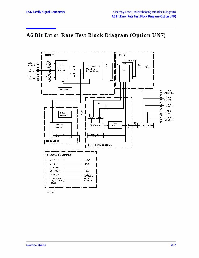
ESG Family Signal Generators Assembly-Level Troubleshooting with Block DiagramsA6 Bit Error Rate Test Block Diagram (Option UN7)
A6 Bit Error Rate Test Block Diagram (Option UN7)
Service Guide 2-7

A7 BASEBAND GENERATOR BLOCK DIAGRAM (OPTIONS UN3 & UN4)
A7 BASEBAND GENERATOR BLOCK DIAGRAM (OPTIONS UN3 & UN4)
DAC
I DATA GENERATION
ANALOG FILTERS(NADC/TETRA/PDC,PHS,GSM)
p
WRITE DATA
LATCH I CAL12
12FORMAT SELECT
p /4 CONTROL LOGIC
/4 CLK
FORMAT SELECT
CA ADDRESS & CONTROL
ICAL LATCHES
I /4 DQPSK
(NADC,TETRA,PDC,PHS)
p
ICONSTANTAMPLITUDE
(GMSK, GFSKDECT)
ABUS
I OUT
P405
I OUT
PATH CONTROLLOGIC
I DACDATA
MODULATIONENABLE/SELECT
TO I-OUT
INT I MOD OUTP301-2
Q DATA GENERATION
WRITE DATA
LATCH Q CAL12 Q
CAL LATCHES
Q OUT
p
p
12FORMAT SELECT
/4 CONTROL LOGIC
/4 CLK
FORMAT SELECT
CA ADDRESS & CONTROL
Q /4 DQPSK
(NADC,TETRA,PDC,PHS)
p
QCONSTANT AMPLITUDE
(GMSK,GFSK,DECT)
Q DACDATA
MODULATIONENABLE/SELECT
MODINVERT DAC
ANALOG FILTERS(NADC/TETRA/PDC,PHS GSM)
ABUS
PATH CONTROLLOGIC
MOD INVERT
P404
Q OUTTO Q-OUT
INT Q MOD OUTP301-53
BURST MOD
EEPROM
DATA
LATCHEDADDRESS
LATCHEDDATA
CONTROLLOGIC
DIGITAL INTERFACE
IAB3P301-26
P301-33EXT SELECT
L EXT STROBEP301-82
P301-83EXT RD L WR
EXT RESETP301-32
P301-24IAB0
IAB1P301-74
P301-25IAB2
P301-76IAB4
IAB5P301-27
P301-77IAB6
IAB7P301-78
P301-29IAB8
IAB9P301-79
P301-36IAB10
READ/LWRITE
STROBE
SELECT
RESET
A0
A1
A2
A3
A4
A5
A6
A7
A8
A9
A10
P301-19EXT_DO
EXT_D1P301-20
P301-70EXT_D2
EXT_D3P301-21
P301-71EXT_D4
EXT_D5P301-72
P301-23EXT_D6
P301-73EXT_D7
D0
DIG BUS INT(PLL UNLOCKED)
D1
D2
D3
D4
D5
D6
D7
SELECT
CLKPLL CLK
PLL LOCK SIG
PLL REF
p
DATA GENERATION CONTROL
CONTROLLOGIC
BURSTCONTROL LOGIC
BURST PLS
MOD INVERT
CAL ENABLE
LATCH I CAL
LATCH Q CAL
PLL GAIN
EXT REF ENABLE
/4 PMF ENABLE
CA PMF ENABLE
VCO ENABLE
EVENT SELECT
PATHCONTROL LOGIC
PMF CONTROL
FORMAT SELECT
LBIT_CLK
LATCH ADDRESS
L_BURST
LATCH DATA
PMFCONTROL
LOGIC
LBIT_CLK
BBG_BIT_CLK
LDATA_CLK
REF
MASTER CLOCK PLL
160 T O 320 MHz
MASTER CLOCK
20 T O 40 MHz
VCOENABLE
F PLL DIVIDERS
VCOABUS
PLL T UNE
PLL_T UNE
P301-35DIG BUS INT(PLL UNLOCKED)
LOOP FILTER&
LEAD/LAG
P300-2222
16BBG_BIT_CLK
P300-16
LOOPCOUNT
&DIFF
ENCODE
INTERNALCLKMASTER CLOCK
LBIT_CLK
BUFFERED DATA
SYMBOL SYNC INV
PMF CONTROL
p /4 CLK
SUB_ I_COUNT (3)
PLL LOCK SIG
SUB_I _COUNT (1)
p
CA ADDRESS & CONTROL
/4 CONTROL LOGIC
P300-22
P300-16
SUB_I_COUNT (1)
PLL_CLOCK
L_BURST
BUFFERED_DATA_IN
SYMBOL_SYNC_INV
ABUS
DATA
RC TIMECONSTANT
LDATA_CLK
ABUS
LCLK
ABUS
BURST
RC TIMECONSTANT
POWER SUPPLY INPUTS
+15V
+10 VREF
ABUS -1V_REF
-1 V_REF
+32VP301-9
P301-14,64
P301-16,66
P301-17,67
P301-12
P301-62
P301-13,63
P301-1,7,54,56
P301-22,28,34,40,46,69,75,81,
87,93 ,99
+5VA
+5.2V
-5.2V
-5V
-15V
ANALOG COMMON
DIGITAL COMMON
+10VREF
BURST MODSWITCH
ANDFILTERS
P301-80L_DCC_ALT_PWR_SEL
INTL_ALC_HOLD
BURST_PULSE
BURST_ENVELOPE
P301-31
P301-30
P301-57
BURSTENVELOPECONTROL
&RAM
ENVL_LATCH
LATCH_DATA
BURST_TC
MASTER_CLK
BURST_PLS
CONTROL LOGIC
DAC_EN
-IV_REF
ENVELOPEDATA
15
15
GENERATOR INTERFACE
REFERENCE
REF SELECT&
DIVIDE
10 MHz DIGP301-84FROM MOTHERBOARD
/CPU
13 MHzFROM 13 MHz IN
P403
P300-6 BURST_GATE
ADJ_TS_PWR_INP300-8
P300-10BB_DATA
SYMBOL_SYNCP300-12
P300-14EXT_CLK
14
12
10
8
6
BBG_INT_CLKP300-18
P300-20BBG_EN
20
18
sk7120a

A7 DBMIC BASEBAND GENERATOR BLOCK DIAGRAM (OPTIONS UN8 and UN9)
s
MASTER CLOCK
30 T O 0 MHz
EEPROM
DATA
LATCHEDADDRESS
LATCHEDDATA
CONTROLLOGIC
DIGITAL INTERFACE
IAB3P1-26
P1-33EXT SELECT
L EXT STROBEP1-82
P1-83EXT RD L WR
EXT RE SETP1-32
P1-24IAB0
IAB1P1-74
P1-25IAB2
P1-76IAB4
IAB5P1-27
P1-77IAB6
IAB7P1-78
P1-29IAB8
IAB9P1-79
P1-36IAB10
READ/LWRITE
STROBE
SELECT
RESET
A0
A1
A2
A3
A4
A5
A6
A7
A8
A9
A10
P1-19EXT_DO
EXT_D1P1-20
P1-70EXT_D2
EXT_D3P1-21
P1-71EXT_D4
EXT_D5P1-72
P1-23EXT_D6
P1-73EXT_D7
D0
DIG_ BUS_ INT(PLL UNLOCKED)
D1
D2
D3
D4
D5
D6
D7
SELECT
CLK
POWER SUPPLY INPUTS
+15V
+10 VREF
+32VP1-9
P1-14,64
P1-16
P1-17,66,67
P1-12
P1-62
P1-13,63
P1-1,7,54,56
P1-22,28,34,40,46,69,75,81,87,93 ,99
+5VA
+3.3VF
-5.2V
-5V
-15V
ANALOG COMMON
DIGITAL COMMON
+10VREF
3VREG
BURST MODABUS
BURST
BURST MODSWITCH
ANDFILTERS
P1-80L_DCC_ALT_PWR_SEL
INTL_ALC_HOLD
BURST_PULSE
BURST_ENVELOPE
P1-31
P1-30
P1-57
BURSTENVELOPECONTROL
&RAM
ENVL_LATCH
L_BURST
LATCH_DATA
+10V_REF
BURST_TC
ALC_HOLD_DIR
ALT_PWR_DIR
MASTER_CLK
BURST_PULSE_DIR
ADJ_TS_PWR_IN
BURST_PLS
CONTROL LOGIC
DAC_EN
ENVELOPEDATA
1515
TA ERATION
ADJDAC
IOFFSET ADJUST
QOFFSET ADJUST
IGAIN ADJUST
QGAIN ADJUST
P2-12
P2-16
P2-14
P2-8
P2-10
14 MHz
FILTER
AUD 2
P1-55
P1-53
J2Q_OUT
RECONSTRUCTION
ABUS
P1-4
I_OFFSET
Q_OFFSET
QDAC
TA ERATION
14 MHz
FILTER
AUD 1P1-6
P1-2
J1I_OUT
RECONSTRUCTION
IDAC
k758b
PLL CLK
PLL LOCK SIG
PLL REF
GENERATOR INTERFACE
REF
MASTER CLOCK PLL
60 T O 120 MHz
6
VCOENABLE
REFERENCE
REF SELECT&
DIVIDE
10 MHz DIGP1-84FROM MOTHERBOARD
/CPU
13 MHzJ3
P403
F PLL DIVIDERS
VCOABUS
PLL T UNE
PLL_T UNE
DIG_BUS_INT(PLL UNLOCKED)
LOOP FILTER&
LEAD/LAG
BURST_GATE LINT_CLK_EN
ADJ_TS LEXT_CLK_EN
EXT_DATA LBBG_EN10
8
6
EXT_SYNC
EXT_CLK14
12
BBG_INT_CLK
BBG_EN20
18
DATA
BBG_TRIG_INT
SYNC
CLK
ALT_PWR_IN
PATTERN_TRG
I_DIRECT
Q_DIRECT
P3-12
P3-14
P3-18
P3-20
P3-6
P3-8
P3-10
P1-49
P1-85
P1-35
P1-100
P1-50
P2-6
P2-4
P10-8,9,10,11,12,13,14,15
P6-12,13,14,15,16,17,18,19
PLL_CLOCK
BURST_GATE
ADJ_TS_PWR_IN
L_BURST
ABUS
LCLK
RC TIMECONSTANT
BUFFERED_DATA_IN
SYMBOL_SYNC
ABUS
DATA
RC TIMECONSTANT
P2-22
16BBG_BIT_CLK
P3-16
EXT_BURST
DIGITAL MODULATOR IC
DIGITAL INTERPOLATOR
FIRPRE-MOD
FILTER
DATA/SYMBOLGENERATOR
Q DAGEN
LATCH DATA BUS
CLK_OUT
DATA_OUT
SYNC_OUT
DATA_EN_OUT
EVENT1_OUT
14
I DAGEN
14
A7 DBMIC BASEBAND GENERATOR BLOCK DIAGRAM (OPTIONS UN8 and UN9)
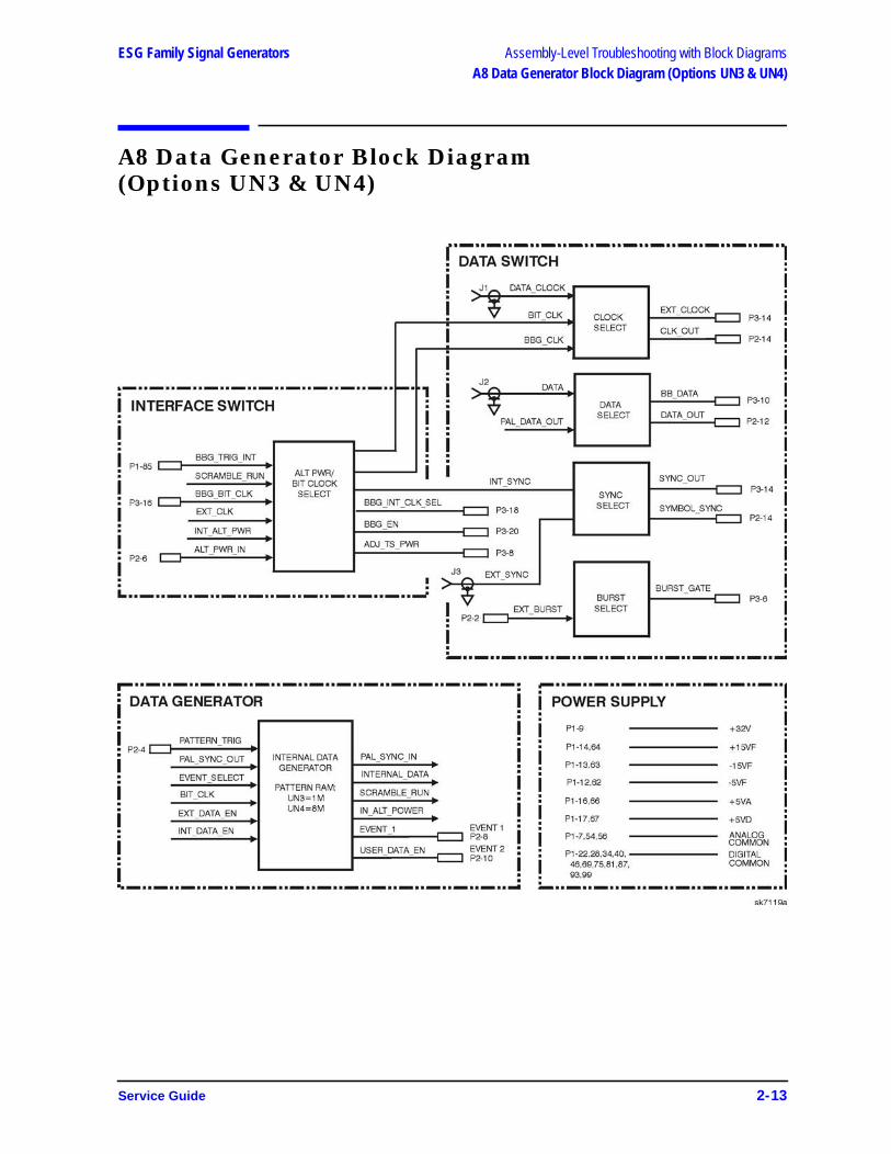
ESG Family Signal Generators Assembly-Level Troubleshooting with Block DiagramsA8 Data Generator Block Diagram (Options UN3 & UN4)
A8 Data Generator Block Diagram(Options UN3 & UN4)
Service Guide 2-13

ESG Family Signal Generators Assembly-Level Troubleshooting with Block DiagramsA8 Data Generator - Rev. A & B Block Diagram (Options UN8 & UN9)
A8 Data Generator - Rev. A & B Block Diagram(Options UN8 & UN9)
Service Guide 2-15
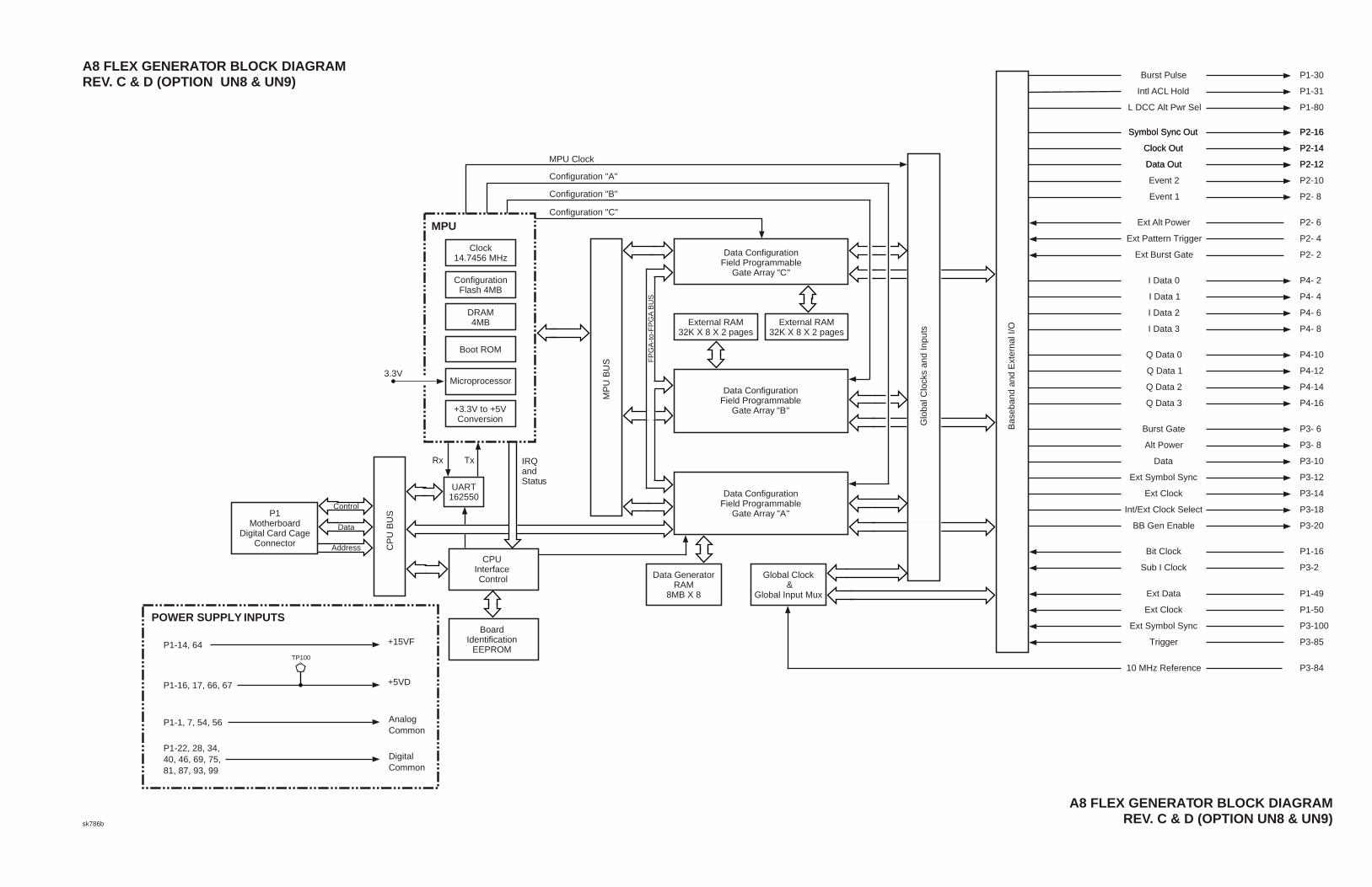
A8 FLEX GENERATOR BLOCK DIAGRAM
A8 FLEX GENERATOR BLOCK DIAGRAM
Data ConfigurationField Programmable
Gate Array "B"
Data ConfigurationField Programmable
Gate Array "A"
Data ConfigurationField Programmable
Gate Array "C"
External RAM32K X 8 X 2 pages
External RAM32K X 8 X 2 pages
Base
band a
nd E
xtern
al I
/O
Symbol Sync OutSymbol Sync Out
Burst Pulse
P2-16P2-16
P1-30
P2-14P2-14
P1-31
P2-12P2-12
P1-80
P2-10
P2- 8
Clock OutClock Out
Intl ACL Hold
Data OutData Out
L DCC Alt Pwr Sel
Event 2
Event 1
P2- 6
P2- 4
P2- 2
Ext Alt Power
Ext Pattern Trigger
Ext Burst Gate
P1-16Bit Clock
P3-2Sub I Clock
P1-49
P1-50
P3-100
P3-85
P3-84
Ext Data
Ext Clock
Ext Symbol Sync
Trigger
10 MHz Reference
P4- 2
P4- 4
P4- 6
P4- 8
I Data 0
I Data 1
I Data 2
I Data 3
P4-10
P4-12
P4-14
P4-16
Q Data 0
Q Data 1
Q Data 2
Q Data 3
P3- 6
P3- 8
P3-10
P3-12
P3-14
P3-18
P3-20
Burst Gate
Alt Power
Data
Ext Symbol Sync
Ext Clock
Int/Ext Clock Select
BB Gen Enable
Data GeneratorRAM
8MB X 8
Global Clock &
Global Input Mux
Glo
bal C
lock
s and Inputs
FP
GA
-to-F
PG
A B
US
REV. C & D (OPTION UN8 & UN9)
POWER SUPPLY INPUTS
P1-14, 64 +15VF
+5VD
AnalogCommon
DigitalCommon
P1-16, 17, 66, 67
P1-1, 7, 54, 56
P1-22, 28, 34,40, 46, 69, 75,81, 87, 93, 99
TP100
MPU Clock
Configuration "C"
Configuration "B"
Configuration "A"
MPU
Clock14.7456 MHz
ConfigurationFlash 4MB
DRAM4MB
Boot ROM
Microprocessor
+3.3V to +5VConversion
3.3V
MP
U B
US
CPUInterface Control
BoardIdentification
EEPROM
CP
U B
US
UART162550
Rx Tx IRQandStatus
P1Motherboard
Digital Card CageConnector
Control
Data
Address
REV. C & D (OPTION UN8 & UN9)sk786b
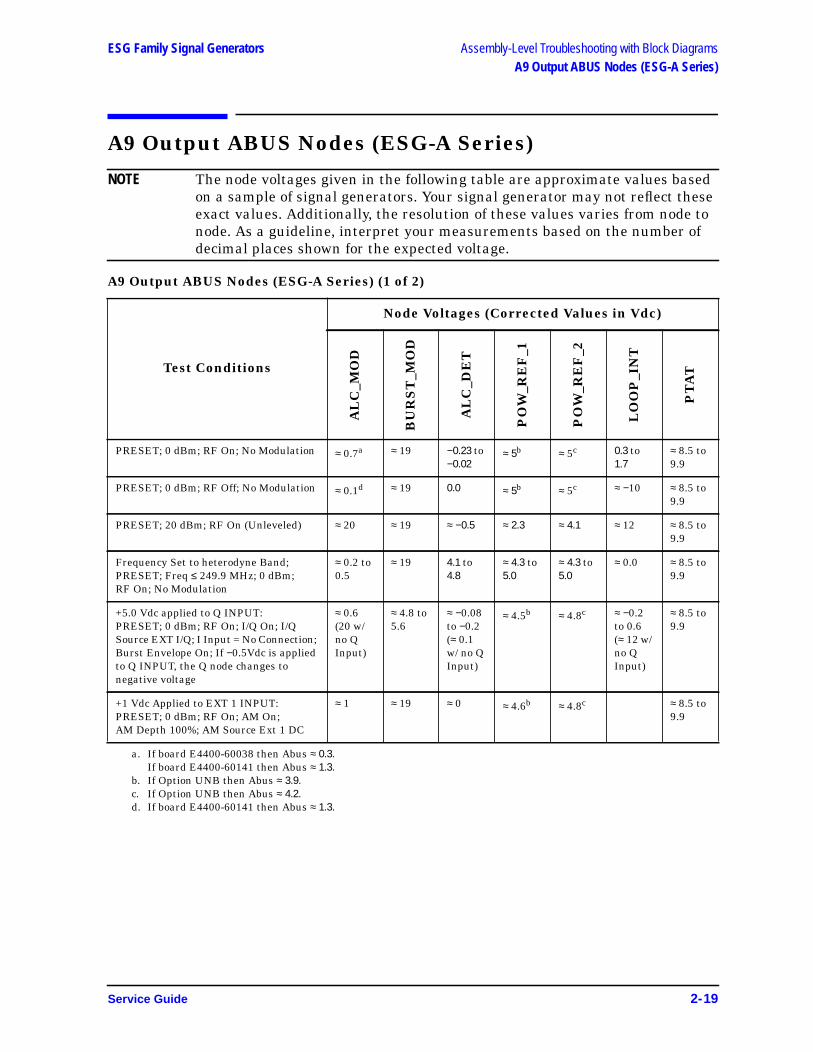
ESG Family Signal Generators Assembly-Level Troubleshooting with Block DiagramsA9 Output ABUS Nodes (ESG-A Series)
A9 Output ABUS Nodes (ESG-A Series)
NOTE The node voltages given in the following table are approximate values basedon a sample of signal generators. Your signal generator may not reflect theseexact values. Additionally, the resolution of these values varies from node tonode. As a guideline, interpret your measurements based on the number ofdecimal places shown for the expected voltage.
A9 Output ABUS Nodes (ESG-A Series) (1 of 2)
Test Conditions
Node Voltages (Corrected Values in Vdc)
AL
C_M
OD
BU
RS
T_M
OD
AL
C_D
ET
PO
W_R
EF
_1
PO
W_R
EF
_2
LO
OP
_IN
T
PT
AT
PRESET; 0 dBm; RF On; No Modulation ≈ 0.7a
a. If board E4400-60038 then Abus ≈ 0.3.If board E4400-60141 then Abus ≈ 1.3.
≈ 19 −0.23 to−0.02
≈ 5b
b. If Option UNB then Abus ≈ 3.9.
≈ 5c
c. If Option UNB then Abus ≈ 4.2.
0.3 to1.7
≈ 8.5 to9.9
PRESET; 0 dBm; RF Off; No Modulation ≈ 0.1d
d. If board E4400-60141 then Abus ≈ 1.3.
≈ 19 0.0 ≈ 5b ≈ 5c ≈ −10 ≈ 8.5 to9.9
PRESET; 20 dBm; RF On (Unleveled) ≈ 20 ≈ 19 ≈ −0.5 ≈ 2.3 ≈ 4.1 ≈ 12 ≈ 8.5 to9.9
Frequency Set to heterodyne Band;PRESET; Freq ≤ 249.9 MHz; 0 dBm;RF On; No Modulation
≈ 0.2 to0.5
≈ 19 4.1 to4.8
≈ 4.3 to5.0
≈ 4.3 to5.0
≈ 0.0 ≈ 8.5 to9.9
+5.0 Vdc applied to Q INPUT:PRESET; 0 dBm; RF On; I/Q On; I/QSource EXT I/Q; I Input = No Connection;Burst Envelope On; If −0.5Vdc is appliedto Q INPUT, the Q node changes tonegative voltage
≈ 0.6(20 w/no QInput)
≈ 4.8 to5.6
≈ −0.08to −0.2(≈ 0.1w/ no QInput)
≈ 4.5b ≈ 4.8c ≈ −0.2to 0.6(≈ 12 w/no QInput)
≈ 8.5 to9.9
+1 Vdc Applied to EXT 1 INPUT:PRESET; 0 dBm; RF On; AM On;AM Depth 100%; AM Source Ext 1 DC
≈ 1 ≈ 19 ≈ 0 ≈ 4.6b ≈ 4.8c ≈ 8.5 to9.9
Service Guide 2-19

Assembly-Level Troubleshooting with Block Diagrams ESG Family Signal GeneratorsA9 Output ABUS Nodes (ESG-A Series)
A9 Output ABUS Nodes (ESG-A Series) (2 of 2)
Test Conditions
Node Voltages (Corrected Values in Vdc)
I Q
PR
E_L
EV
EL
QU
AD
GA
IN_D
ET
GN
D
RE
F_A
M
PRESET; 0 dBm; RF On; No Modulation ≈ 0.7 ≈ 0 ≈ 2.1a
a. If board E4400-60155, 60141 or 60038 then Abus ≈ 3.
≈ −1.8 −0.22tob
−0.05
b. If board E4400-60038 then Abus ≈ 1.2.
0.0 −0.52toc
0.3
c. If Option UNB then Abus ≈ 0.8.
PRESET; 0 dBm; RF Off; No Modulation ≈ 0.7 ≈ 0 ≈ 2.1d
d. If board E4400-60038 then Abus ≈ 5.0.If board E4400-60155 or 60141 then Abus ≈ 3.
≈ −1.8 −0.22tob
−0.05
0.0 ≈ −0.52toc
0.3
PRESET; 20 dBm; RF On (Unleveled) ≈ 0.7 ≈ 0 ≈ 2.1a ≈ −1.8 −0.3 tob
−0.190.0 ≈ 2.3
Frequency Set to heterodyne Band;PRESET; Freq ≤ 249.9 MHz; 0 dBm;RF On; No Modulation
≈ 0.44 ≈ 0 ≈ 2e
e. If board E4400-60155 or 60141 then Abus ≈ 4.
≈ −3 ≈ −0.04b 0.0 −0.1 to0.6
+5.0 Vdc applied to Q INPUT:PRESET; 0 dBm; RF On; I/Q On; I/QSource EXT I/Q; I Input = No Connection;Burst Envelope On; If −0.5Vdc is appliedto Q INPUT, the Q node changes tonegative voltage
≈ 0.0 ≈ 1.1 ≈ 2f
f. If board E4400-60155 or 60141 then Abus ≈ 3.
≈ −1.8 ≈ 0.6(0.0 w/no QInput)
0.0 0.2 to0.9
+1 Vdc Applied to EXT 1 INPUT:PRESET; 0 dBm; RF On; AM On;AM Depth 100%; AM Source Ext 1 DC
≈ 0.7 ≈ 0 ≈ 2.1a ≈ −1.8 ≈ −0.2 0.0 ≈ 0.9g
g. If Option UNB then Abus ≈ 1.4.
2-20 Service Guide

A9 OUTPUT BLOCK DIAGRAM (ESG-A SERIES)
BURST MOD
ALC MODDRIVE
BURST MODDRIVE
MIXER700 - 1050 MHzBPF
300 MHzLPF
1 GHz REFERENCEP1-19
FROM: REFERENCEASSY P1-19
00 MHZ LPF
50 MHZ LPF
00 MHZ LPF
28 MHZ LPF
96 MHZ LPF
F >250 MHz
F < 250 MHz F <250 MHz
F >250 MHz
250 MHz TO 4000 MHz0 dBm +/- 5dB
DET BWSEL
DETVOLTAGE
RF OUT
.250 TO 4000 MHzMAX POWER >17 dBm
TO: STEP ATTENUATORASSY J2
2400-4000MHz
1550-2400
1000-1550
628-1000
396-628
256-396
GAIN ADJ DET
ALC MOD
LO
J6
1GHZ
ABUS
PRELEVEL
PRELEVEL DET
PRELEVEL REF
+
DAC
PRELEVEL MOD DRIVEP3-4
TO: SYNTHESIZER P3-17
SELECT
DATA
CLK
CLK
DATA
ENABLE/INTRPT
INT 1
INT2
INT3
INT4 (Serial Data)
SERIAL I/O
DIGITALCONTROL
EEPROM
+5V
+5V
EVELED
+5V
L INTERFACE MUX
ALC MOD 1BURST MODLOOP INTREF PLUS AMPRELEVEL DRIVEALC DET
PWR REF
+PTAT
ABUSP1-4
ABUS
ABUS
R SUPPLIES INPUTS
+15VF
+9VF
+5VF
-6VF
-15VF
ANALOG COMMON
DIGITAL COMMON
TEMPERATURECOMPENSATIONPOWER SUPPLY
PTAT
GND
+PTATP1-15
8.5 TO 9.9V
ILTER
ILTER
ILTER
ILTER
ILTER -PTAT
+10V REG +10V
ABUS
DET OFFSET
LOGAMP
ABUSABUS
DETVOLTAGE
ALT ALC REF
ALC REF
BULK R ADJUSTMENT
LOG DET
ALC DET
ALC REFSELECT
CLOSED=OPEN LOOP
IN BAND AM
PWR REF
REF + AM
REF AM
LOG OFFSET
ALC DETECTOR
ALC REFERENCE REFERENCE + AM
DAC
DAC
DAC
DAC
OPEN =HOLD MAIN INT
CLOSED =RF OFF ALT INT
CLOSED =RF OFF MAIN INT
OPEN =HOLD ALT INT
+V
+V
ABUS
LOOP INT
ALC MOD BIAS
ABUS
ALC MOD
ALC UNLEVELEDDETECTOR
+
+
_
_
-15V
OPEN =OPEN LOOP
CLOSED =RF OFF (ALC MOD)
ALC MODDRIVER
ALT POWERSELECT LOGIC
BW SELECT
BW SELECT
L ALT PWR SEL
P2-10
FEED FORWARD AM
ALT POWER SELECT
L_UNLEVELED
ALC MOD DRIVE
ALC REF SELECT
ALC MOD DRIVE
DAC
P1-2
EN LIN AM
LIN_AM_ MODAMPLOG
BURSTMOD
DRIVER
ABUS
&
&BURST MOD OFFSET
BURST MOD BIAS
-6V
CLOSED =RF OFF(BURST MOD)
L RF OFF (BURST MOD)PULSE MOD
P2-23FROM: REFERENCE ASSYP3-7
ALT POWER SELECT
L ALC HOLD
L HOLD ALC
DEEP AM LEVEL DETECTORREF + AMDEEP AM MOD
L RF OFF ALC MOD
HOLD MAININT
HOLD ALTINT
FEED FORWARD AM
BURSTMODDRIVE
BURST MOD
BURST EN
BURST GAIN
REF
EN LIN BURST
EN LOG BURST
FADE ENVELOPE(NOT USED)
BURST ENVELOPE(NOT USED)
P1-17
P1-6
FROM: REFERENCEASSYP3-17
P2-22
AM INPUT
BURST MOD DRIVE ALC HOLD
OPEN=OPEN LOOP
DAC
DAC
DAC
24
15
10
6
3
RF PATH
FROM:SYNTHESIZER
J4RF IN
250 to 4000 MHz>+10 dBm
ENABLE/INTERRUPTP2-25
CLK OUT P2-24
DATA P2-11
L UNL
DIGITA
POWE
P2-6,21
P2-15,30
P2-1,16
P2-1,17
P2-3,18
P2-14,29
P2-5,20
F
F
F
F
F
A9 OUTPUT BLOCK DIAGRAM (ESG-A SERIES)
sk785b

ESG Family Signal Generators Assembly-Level Troubleshooting with Block DiagramsA9 Output ABUS Nodes (ESG-D Series)
A9 Output ABUS Nodes (ESG-D Series)
NOTE The node voltages given in the following table are approximate values basedon a sample of signal generators. Your signal generator may not reflect theseexact values. Additionally, the resolution of these values varies from node tonode. As a guideline, interpret your measurements based on the number ofdecimal places shown for the expected voltage.
A9 Output ABUS Nodes (ESG-D Series) (1 of 2)
Test Conditions
Node Voltages (Corrected Values in Vdc)
AL
C_M
OD
BU
RS
T_M
OD
AL
C_D
ET
PO
W_R
EF
_1
PO
W_R
EF
_2
LO
OP
_IN
T
PT
AT
PRESET; 0 dBm; RF On; No Modulation ≈ 0.7a
a. If board E4400-60038 then Abus ≈ 0.3.If board E4400-60141 then Abus ≈ 1.3.
≈ 19 −0.23 to−0.02
≈ 5b
b. If Option UNB then Abus ≈ 3.9.
≈ 5c
c. If Option UNB then Abus ≈ 4.2.
0.3 to1.7
≈ 8.5 to9.9
PRESET; 0 dBm; RF Off; No Modulation ≈ 0.1d
d. If board E4400-60141 then Abus ≈ 1.3.
≈ 19 0.0 ≈ 5b ≈ 5c ≈ −10 ≈ 8.5 to9.9
PRESET; 20 dBm; RF On (Unleveled) ≈ 20 ≈ 19 ≈ −0.5 ≈ 2.3 ≈ 4.1 ≈ 12 ≈ 8.5 to9.9
Frequency Set to heterodyne Band;PRESET; Freq ≤ 249.9 MHz; 0 dBm;RF On; No Modulation
≈ 0.2 to0.5
≈ 19 4.1 to4.8
≈ 4.3 to5.0
≈ 4.3 το5.0
≈ 0.0 ≈ 8.5 to9.9
+5.0 Vdc applied to Q INPUT:PRESET; 0 dBm; RF On; I/Q On; I/QSource EXT I/Q; I Input = No Connection;Burst Envelope On; If −0.5Vdc is appliedto Q INPUT, the Q node changes tonegative voltage
≈ 0.6(20 w/no QInput)
≈ 4.8 to5.6
≈ −0.08to −0.2(≈ 0.1w/ no QInput)
≈ 4.5b ≈ 4.8c ≈ −0.2to 0.6(≈ 12 w/no QInput)
≈ 8.5 to9.9
+1 Vdc Applied to EXT 1 INPUT:PRESET; 0 dBm; RF On; AM On;AM Depth 100%; AM Source Ext 1 DC
≈ 1 ≈ 19 ≈ 0 ≈ 4.6b ≈ 4.8c ≈ 8.5 to9.9
Service Guide 2-23
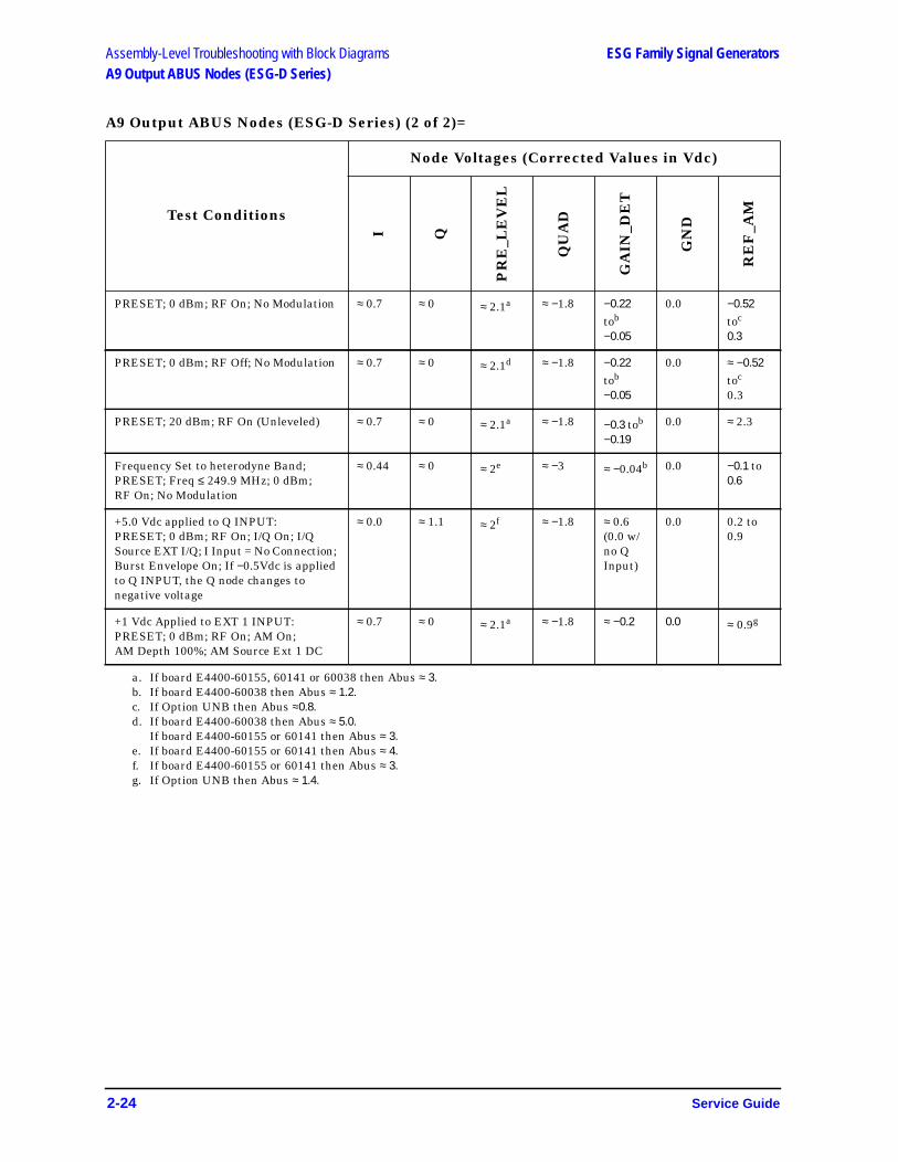
Assembly-Level Troubleshooting with Block Diagrams ESG Family Signal GeneratorsA9 Output ABUS Nodes (ESG-D Series)
A9 Output ABUS Nodes (ESG-D Series) (2 of 2)=
Test Conditions
Node Voltages (Corrected Values in Vdc)
I Q
PR
E_L
EV
EL
QU
AD
GA
IN_D
ET
GN
D
RE
F_A
M
PRESET; 0 dBm; RF On; No Modulation ≈ 0.7 ≈ 0 ≈ 2.1a
a. If board E4400-60155, 60141 or 60038 then Abus ≈ 3.
≈ −1.8 −0.22tob
−0.05
b. If board E4400-60038 then Abus ≈ 1.2.
0.0 −0.52toc
0.3
c. If Option UNB then Abus ≈0.8.
PRESET; 0 dBm; RF Off; No Modulation ≈ 0.7 ≈ 0 ≈ 2.1d
d. If board E4400-60038 then Abus ≈ 5.0.If board E4400-60155 or 60141 then Abus ≈ 3.
≈ −1.8 −0.22tob
−0.05
0.0 ≈ −0.52toc
0.3
PRESET; 20 dBm; RF On (Unleveled) ≈ 0.7 ≈ 0 ≈ 2.1a ≈ −1.8 −0.3 tob
−0.190.0 ≈ 2.3
Frequency Set to heterodyne Band;PRESET; Freq ≤ 249.9 MHz; 0 dBm;RF On; No Modulation
≈ 0.44 ≈ 0 ≈ 2e
e. If board E4400-60155 or 60141 then Abus ≈ 4.
≈ −3 ≈ −0.04b 0.0 −0.1 to0.6
+5.0 Vdc applied to Q INPUT:PRESET; 0 dBm; RF On; I/Q On; I/QSource EXT I/Q; I Input = No Connection;Burst Envelope On; If −0.5Vdc is appliedto Q INPUT, the Q node changes tonegative voltage
≈ 0.0 ≈ 1.1 ≈ 2f
f. If board E4400-60155 or 60141 then Abus ≈ 3.
≈ −1.8 ≈ 0.6(0.0 w/no QInput)
0.0 0.2 to0.9
+1 Vdc Applied to EXT 1 INPUT:PRESET; 0 dBm; RF On; AM On;AM Depth 100%; AM Source Ext 1 DC
≈ 0.7 ≈ 0 ≈ 2.1a ≈ −1.8 ≈ −0.2 0.0 ≈ 0.9g
g. If Option UNB then Abus ≈ 1.4.
2-24 Service Guide

ESG Family Signal Generators Assembly-Level Troubleshooting with Block DiagramsA9 Output ABUS Nodes (ESG-AP, & ESG-DP Series)
A9 Output ABUS Nodes(ESG-AP, & ESG-DP Series)
NOTE The node voltages given in the following table are approximate values basedon a sample of signal generators. Your signal generator may not reflect theseexact values. Additionally, the resolution of these values varies from node tonode. As a guideline, interpret your measurements based on the number ofdecimal places shown for the expected voltage.
A9 Output ABUS Nodes (ESG-AP & ESG-DP Series) (1 of 2)
A9 Output ABUS Nodes (ESG-AP & ESG-DP Series) (2 of 2)
TestConditions
Node Voltages (Corrected Values in Vdc)
AL
C_M
OD
BU
RS
T_M
OD
AL
C_D
ET
PO
W_R
EF
_1
PO
W_R
EF
_2
LO
OP
_IN
T
PT
AT
PRESET;0 dBm; RF On;No Modulation;50 Ω load onoutput
≈ 0.2 to 2a
a. These values will be > 10 V if ALC is unleveled.
≈ 0.5 to 5 at≤ 2.4 GHz;≤ 20 at4 GHz
−0.3 3.5 4.2 ≈ −2 to 2a
(varies w/freq)
9.5(8.5 to 9.9)
TestConditions
Node Voltages (Corrected Values in Vdc)
I Q
PR
E_L
EV
EL
QU
AD
GA
IN_D
ET
GN
D
RE
F_A
M
PRESET;0 dBm; RF On;No Modulation;50 Ω load onoutput
1.9 0 ≈ −2 to 12(varies w/freq)
0.7 −0.35 to0.02 at≤ 2.4 GHz;0.1 to 0.7 at> 2.4 GHz
0 ≈ 0.6(varies w/freq &powerlevel)
Service Guide 2-25

A9 OUTPUT BLOCK DIAGRAM
ABUS
BURST MOD
ALC MODDRIVE
BURST MODDRIVE
MIXER700 - 1050 MHzBPF
300 MHzLPF
1 GHz REFERENCEP1-19
FROM: REFERENCEASSY P1-19
00 MHZ LPF
50 MHZ LPF
00 MHZ LPF
28 MHZ LPF
96 MHZ LPF
GAIN DETECTOR
F >250 MHz
F < 250 MHz F <250 MHz
F >250 MHz
250 MHz TO 4000 MHz0 dBm + -5dB
DET BWSEL
DETVOLTAGE
RF OUT
.250 TO 4000 MHzMAX POWER >17 dBm
TO: STEP ATTENUATORASSY J2
2400-4000MHz
1550-2400
1000-1550
628-1000
396-628
256-396
GAIN ADJ DET
ALC MOD
LO
J6
1GHZ
ABUS
I OFFSET
Q OFFSET
DAC
DAC
DAC
I GAIN
Q GAIN
I MOD SELECTFROM: REFERENCEASSY
Q MOD SELECT
P3-6
INT_I_MOD
EXT_I_MOD
EXT_Q_MOD
INT_Q_MOD
EXT_Q_MOD
EXT_I_MOD
CALVOLTAGES
CALVOLTAGES
REF
REF
ISTEP
ATTENUATOR
QSTEP
ATTENUATORQ MOD DRIVE
ABUS
I MOD DRIVE
P3-15
-19
EXT Q MOD
EXT I MOD
-8
M: Q INPUT
OM: I INPUT
I MOD DRIVE
Q MOD DRIVE
DAC
ABUS
DET OFFSET
DAC
LOGAMP
ABUSABUS
DAC
DAC
DAC
DETVOLTAGE
ALT ALC REF
ALC REF
BULK R ADJUSTMENT
LOG DET
ALC DET
ALC REFSELECT
CLOSED=OPEN LOOP
IN BAND AM
PWR REF
REF + AM
REF AM
LOG OFFSET
ALC DETECTOR
ALC REFERENCE REFERENCE + AM
DAC
OPEN =HOLD MAIN INT
CLOSED =RF OFF ALT INT
CLOSED =RF OFF MAIN INT
OPEN =HOLD ALT INT
+V
+V
ABUS
LOOP INT
ALC MOD BIAS
ABUS
ALC MOD
ALC UNLEVELEDDETECTOR
+
+
_
_
-15V
OPEN =OPEN LOOP
CLOSED =RF OFF (ALC MOD)
ALC MODDRIVER
ALT POWERSELECT LOGIC
BW SELECT
BW SELECT
FROM: BASEBAND GENERATOR ASSY P301-80
L ALT PWR SEL
P2-10
FEED FORWARD AM
ALT POWER SELECT
L_UNLEVELED
ALC MOD DRIVE
ALC REF SELECT
ALC MOD DRIVE
P1-2
EN LIN AM
LIN_AM_ MODAMPLOG
BURSTMOD
DRIVER
ABUS
DAC
DAC
DAC
&
&BURST MOD OFFSET
BURST MOD BIAS-6V
CLOSED =RF OFF(BURST MOD)
L RF OFF (BURST MOD)PULSE MOD
P2-23FROM: REFERENCE ASSYP3-7
FROM: BASEBAND GENERATOR ASSYP301-31
ALT POWER SELECT
L ALC HOLD
L HOLD ALC
DEEP AM LEVEL DETECTORREF + AMDEEP AM MOD
L RF OFF ALC MOD
HOLD MAININT
HOLD ALTINT
FEED FORWARD AM
BURSTMODDRIVE
BURST MOD
BURST ENBURST GAIN
REF
EN LIN BURST
EN LOG BURST
FADE ENVELOPE(NOT USED)
BURST ENVELOPE
P1-17
P1-6
FROM: BASEBANDGENERATOR ASSYP301-57
FROM: REFERENCEASSYP3-17
P2-22
AM INPUT
BURST MOD DRIVE ALC HOLD
OPEN=OPEN LOOP
(ESG-D, ESG-AP, & ESG-DP SERIES)
DAC
DAC
DAC
ABUS
ABUS
I/QMODULATOR
VBLO QUAD Q I
I DET Q DET
AUX OUTTO: COHERENT
CARRIER OUT
RF IN250 to 4000 MHz
>+10 dBm
FROM: SYNTHESIZER
OR FRAC-N/DIVIDER
J4
PRELEVEL DET
PRELEVEL
PRELEVEL REF
PRELEVEL MOD DRIVEP3-4
TO: SYNTHESIZER OR ASSY
P3-17FRAC-N/DIVIDER
GAIN ADJUST
I MOD DRIVE
Q MOD DRIVE
QUADVBLO DAC
24
15
10
6
3
RF PATH
J5
+
QUADDAC
QUADCONTROL
LOOP
GAIN ADJMOD
ENABLE/INTERRUPTP2-25
SELECT
DATA
CLK
CLK
DATA
ENABLE/INTRPT
INT 1
INT2
INT3
INT4 (Serial Data)
SERIAL I/O
DIGITALCONTROL
EEPROM
CLK P2-24
DATA P2-11
+5V
+5V
L UNLEVELED
+5V
DIGITAL INTERFACE MUXALC MOD 1BURST MODLOOP INTREF PLUS AMPRELEVEL DRIVEQUAD LOOPGAIN ADJUST DETIQALC DET
PWR REF
+PTAT
ABUSP1-4
ABUS
ABUS
POWER SUPPLIES INPUTS
P2-6,21 +15VF
+9VF
+5VF
-6VF
-15VF
ANALOG COMMON
DIGITAL COMMON
TEMPERATURECOMPENSATIONPOWER SUPPLY
PTAT
GND
+PTATP1-15
8.5 TO 9.9V
P2-15,30
P2-1,16
P2-1,17
P2-3,18
P2-14,29
P2-5,20
FILTER
FILTER
FILTER
FILTER
FILTER -PTAT
+10V REG +10V
P3
P3
FRO
FR
A9 OUTPUT BLOCK DIAGRAM(ESG-D, ESG-DP, & ESG-DP SERIES)sk772b

ESG Family Signal Generators Assembly-Level Troubleshooting with Block DiagramsA11 Reference ABUS Nodes (ESG-A & ESG-D Series)
A11 Reference ABUS Nodes(ESG-A & ESG-D Series)
NOTE The node voltages given in the following table are approximate values basedon a sample of signal generators. Your signal generator may not reflect theseexact values. Additionally, the resolution of these values varies from node tonode. As a guideline, interpret your measurements based on the number ofdecimal places shown for the expected voltage.
A11 Reference ABUS Nodes (ESG-A & ESG-D Series)
Test Conditions
Node Voltages (Corrected Values in Vdc)M
OD
1_O
UT
MO
D2_
OU
T
VT
UN
E
MO
D1_
PK
MO
D2_
PK
LIN
_AM
1GH
Z_D
ET
FM
_MO
D
PRESET; No Modulation 0.00 0.00 2 to 4 < 0.5 < 0.5 0.00 0.0 < 0.3
Frequency Set to Heterodyne Band:PRESET; Freq ≤ 249.9 MHz;No Modulation
2 to 4 > 0.15
+1 Vdc Applied to EXT 1 INPUT:PRESET; FM On; FM Source Ext 1 DC
≈ −1.9 0.00 2 to 4 < 0.5 < 0.5 0.0 ≈ 2.2
+1 Vdc Applied to EXT 2 INPUT:PRESET; FM On; FM Source Ext 2 DC
≈ 0 0.00 2 to 4 ≈ 7.5 < 0.5 0.0 ≈0
1 Vpp @ 1 kHz Applied to EXT 1 INPUT:PRESET; FM On; FM Source Ext 1 AC
≈ −1.9 0.00 2 to 4 < 0.5 < 0.5 ≈ 2.0 0.0
1 Vpp @ 1 kHz Applied to EXT 2 INPUT:PRESET; FM On; FM Source Ext 2 AC
≈ 0 0.00 2 to 4 ≈ 7.5 < 0.5 ≈ 0 0.0
+1 Vdc Applied to EXT 1 INPUT:PRESET; AM On; AM Depth 100%;AM Source Ext 1 DC
0.00 ≈ −1.9 2 to 4 < 0.5 < 0.5 0.0 ≈ 2.2
+1 Vdc Applied to EXT 2 INPUT:PRESET; AM On; AM Depth 100%;AM Source Ext 2 DC
0.00 ≈ 0 2 to 4 < 0.5 ≈ 7.5 0.0 ≈ 0
1 Vpp @ 1 kHz Applied to EXT 1 INPUT:PRESET; AM On; AM Depth 100%;AM Source Ext 1 AC
0.00 ≈ −1.9 2 to 4 < 0.5 < 0.5 ≈ 2.0 0.0
1 Vpp @ 1 kHz Applied to EXT 2 INPUT:PRESET; AM On; AM Depth 100%;AM Source Ext 2 AC
0.00 ≈ 0 2 to 4 < 0.5 ≈ 7.5 ≈ 0 0.0
Service Guide 2-29
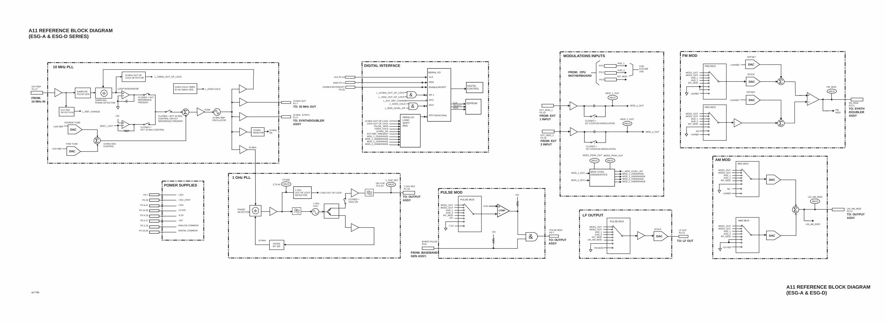
A(
A11 REFERENCE BLOCK DIAGRAM(ESG-A & ESG-D)
10 MHz
10 MHzMONITOR
1 GHz PLL
FPHASEDETECTOR
DIVIDEBY 100
1 GHzOUT OF LOCKDETECTOR
CLOSED =1GHz ON
1 GHzVCO
ABUS
VTUNE
2 T0 4V ABUS
1_GHZ_DET
ON: 0.05 T0 0.3V 1 GHz REF
P1-19
1 GHZ OUT OF LOCK
10 MHz
DIGITAL INTERFACE
CLKSELECTDATA
CLK
DATA
ENABLE/INTRPT
INT 1
INT2
INT3
INT4 (Serial Data)
SERIAL I/O
DIGITALCONTROL
EEPROM
PARALLELLOADSHIFTREG
10 MHz OUT OF LOCK1GHz OUT OF LOCK
PULSE_ MODOVEN_COLD
10 MHz_OKEXT REF_PRESENTMOD_1_OVERANGE
MOD_1_UNDERANGEMOD_2_OVERANGE
MOD_2_UNDERANGE
&L_OVEN_COLD
L_MOD_LEVEL_INT
&L_10 MHz_OUT_OF_LOCK
L_1GHz_OUT_OF_LOCK
CLK P2-24
DATA P2-11
ENABLE/INTERRUPTP2-25
10 MHz OUTP1-7
TO: 10 MHz OUT
10 MHz SYNTHP1-5
TO: SYNTH/DOUBLERASSY
10 MHzOK
MODULATIONS INPUTS
ABUS
ABUS
MOD_1_OUT
MOD_2_OUT
FOR FUTURE USE
AUD_1
AUD_2
INT_MOD
P3-5
P3-2
P3-6
FROM: CPUMOTHERBOARD
MOD_1_OUT
MOD_2_OUT
CLOSED =DC COUPLED MODULATION
CLOSED =DC COUPLED MODULATION
MOD LEVELDIAGNOSTICS
ABUSABUS
MOD1_PEAK_OUT MOD2_PEAK_OUT
MOD_1_OUT
MOD_2_OUT
L_MOD_LEVEL_INTMOD_1_OVERANGEMOD_1_UNDERANGEMOD_2_OVERANGEMOD_2_UNDERANGE
EXT_MOD_1P3-19
FROM: EXT 1 INPUT
EXT_MOD_2P3-10
FROM: EXT 2 INPUT
+
PULSE MOD
PULSE MUX
&
MOD1_OUTMOD2_OUT
AUD_1AUD_2
INT_MOD+5V
-7.5V
COMP
+COMP
+-0.6V
PULSE MODP3-7
TO: OUTPUTASSY
+5V
+5V
LF OUTPUT
DAC
PULSE MUX
MOD1_OUTMOD2_OUT
AUD_1AUD_2
INT_MODLIN_AM_MOD
FM.MOD
LF OUTP3-13
TO: LF OUT
SCALE
FM MOD
ABUS
FM_MOD
DAC
DAC
DACFM2 MUX
FM1 MUX
MOD1_OUTMOD2_OUT
AUD_1AUD_2
INT_MOD
MOD1_OUTMOD2_OUT
AUD_1AUD_2
INT_MOD
+2VREF
+2VREF
NC
AM MOD
ABUS
LIN_AM_MOD
DAC
AM1 MUX
MOD1_OUTMOD2_OUT
AUD_1AUD_2
INT_MOD
+2VREF
NC
DAC
AM2 MUX
MOD1_OUTMOD2_OUT
AUD_1AUD_2
INT_MOD
+2V REF
LIN_AM_MODP3-17
TO: OUTPUT ASSY
FM_MODP3-11
TO: SYNTH/DOUBLER ASSY
+10VREF
+10VREF
OFFSET
SCALE
OFFSET
TO: OUTPUTASSY
L_EXT_REF_CHANGE
FMMOD
LIN_AM_MOD
BURST PULSEP3-8
FROM: BASEBANDGEN ASSY.
10 MHz PLL
11 REFERENCE BLOCK DIAGRAMESG-A & ESG-D SERIES)
EXT REFP1-17
FROM:10 MHz IN
SAMPLERPULSE GEN
SAMPLINGPHASE DETECTOR
10 MHz OUT OFLOCK DETECTOR
EXT REFDETECTION L_REF_CHANGE
10 MHz DACCONTROL
COURSE TUNE
+10V REF
+10V REF
DAC
DAC
FINE TUNE
F ++--
++--
CLOSED =EXT 10 MHz CONTROL
+3V
MOD_I_OUT
CLOSED = EXT 10 MHzCONTROL OR EXT REFERENCE PRESENT
CLOSED = EXT REFERENCEPRESENT
L_10MHz_OUT_OF_LOCK
LOOP INTEGRATOR
TUNE
OVEN COLD TIMER(5 min Option 1E5) L_OVEN COLD
10 MHz REFOSCILLATOR
sk778b
POWER SUPPLIES
P2-7
P2-26
P2-6,21
P2-14,29
P2-4,19
P2-2,17
P2-1,16
P2-15,30
+32V
+15V_STBY
+15V
+5.2VD
-5.2V
-15V
ANALOG COMMON
DIGITAL COMMON

ESG Family Signal Generators Assembly-Level Troubleshooting with Block DiagramsA11 Reference ABUS Nodes (ESG-AP & ESG-DP Series)
A11 Reference ABUS Nodes(ESG-AP & ESG-DP Series)
NOTE The node voltages given in the following table are approximate values basedon a sample of signal generators. Your signal generator may not reflect theseexact values. Additionally, the resolution of these values varies from node tonode. As a guideline, interpret your measurements based on the number ofdecimal places shown for the expected voltage.
A11 Reference ABUS Nodes (ESG-AP & ESG-DP Series)
Test Conditions
Node Voltages (Corrected Values in Vdc)M
OD
1_O
UT
MO
D2_
OU
T
VT
UN
E
MO
D1_
PK
MO
D2_
PK
LIN
_AM
1GH
Z_D
ET
FM
_MO
D
PRESET; 0 dBm; RF On; No Modulation ≈ 0 ≈ 0 7 to 27(Fixedvs.Freq)
0.5 0.5 ≈ 0 ≈ 0.25(< 250MHz)
≈ 0.02(> 250MHz)
< 0.3
Service Guide 2-33

COLD
0 MHz REFSCILLATOR
10 MHz
10 MHzMONITOR
10 MHz OUTP1-7TO: 10 MHz OUT» +7dBm
10 MHz SYNTHP1-5TO: FRAC-N/DIVIDERASSY» +7dBm
10 MHzOK
1 GHz PLL
FPHASEDETECTOR
DIVIDEBY 100
1 GHzOUT OF LOCKDETECTOR
CLOSED =HET BAND1 GHz
VCO
ABUS
VTUNE
2 T0 4V ABUS
1_GHZ_DET
ON: 0.05 T0 0.3V
1 GHz REFP1-19
1 GHZ OUT OF LOCK
10 MHz
TO: OUTPUTASSY
BPF
1GHz
1GHzJ3 TOSAMPLER BD.
DIGITAL INTERFACE
CLKSELECTDATA
CLK
DATA
ENABLE/INTRPT
SERIAL I/O
DIGITALCONTROL
EEPROM
PARALLELLOADSHIFTREG
10 MHz OUT OF LOCK1GHz OUT OF LOCK
PULSE_ MODOVEN_COLD
10 MHz_OKEXT REF_PRESENTMOD_1_OVERANGE
MOD_1_UNDERANGEMOD_2_OVERANGE
MOD_2_UNDERANGE
&L_OVEN_COLD
L_MOD_LEVEL_INT
&L_10 MHz_OUT_OF_LOCK
L_1GHz_OUT_OF_LOCK
CLK P2-24
DATA P2-11
ENABLE/INTERRUPTP2-25
L_EXT_REF_CHANGE
INT 1
INT2
INT3
INT4 (Serial Data)
MOD1_OUTMOD2_OUT
V TUNEMOD1_PEAK_OUTMOD2_PEAK_OUT
LIN_AM_MOD1 GHz_DET
FM_MOD
P2-9
ABUS
PULSE MOD
PULSE MUX
&
MOD1_OUTMOD2_OUT
AUD_1AUD_2
INT_MOD+5V
-7.5V
COMP
+
COMP
+-0.6V
PULSE MODP3-7
TO: OUTPUTASSY
+5V
+5V
BURST PULSEP3-8
FROM: BASEBANDGEN ASSY.
MODULATIONS INPUTS
ABUS
ABUS
MOD_1_OUT
MOD_2_OUT
FOR FUTURE USE
AUD_1
AUD_2
INT_MOD
P3-5
P3-2
P3-6
FROM: CPUMOTHERBOARD
MOD_1_OUT
MOD_2_OUT
CLOSED =DC COUPLED MODULATION
CLOSED =DC COUPLED MODULATION
MOD LEVELDIAGNOSTICS
ABUSABUS
MOD1_PEAK_OUT MOD2_PEAK_OUT
MOD_1_OUT
MOD_2_OUT
L_MOD_LEVEL_INTMOD_1_OVERANGEMOD_1_UNDERANGEMOD_2_OVERANGEMOD_2_UNDERANGE
EXT_MOD_1P3-19FROM: EXT 1 INPUT
EXT_MOD_2P3-10FROM: EXT 2 INPUT
LF OUTPUT
DAC
PULSE MUX
MOD1_OUTMOD2_OUT
AUD_1AUD_2
INT_MODLIN_AM_MOD
FM.MOD
LF OUTP3-13
TO: LF OUT
SCALE
+
FM MOD
ABUS
FM_MOD
DAC
DAC
DACFM2 MUX
FM1 MUX
MOD1_OUTMOD2_OUT
AUD_1AUD_2
INT_MOD
MOD1_OUTMOD2_OUT
AUD_1AUD_2
INT_MOD
+2VREF
+2VREF
NC
FM_MODP3-11TO: FRAC-N/DIVIDERASSY
+10VREF
+10VREF
OFFSET
SCALE
OFFSET
FMMOD
A11 REFERENCE BLOCK DIAGRAM (ESG-AP & ESG-DP SERIES)
AM MOD
ABUS
LIN_AM_MOD
DAC
AM1 MUX
MOD1_OUTMOD2_OUT
AUD_1AUD_2
INT_MOD
+2VREF
NC
DAC
AM2 MUX
MOD1_OUTMOD2_OUT
AUD_1AUD_2
INT_MOD
+2V REF
LIN_AM_MODP3-17TO: OUTPUT ASSY
LIN_AM_MOD
10 MHz PLL
A11 REFERENCE BLOCK DIAGRAM (ESG-AP & ESG-DP SERIES)
EXT REFP1-17
FROM:10 MHz IN
SAMPLERPULSE GEN
SAMPLINGPHASE DETECTOR
10 MHz OUT OFLOCK DETECTOR
EXT REFDETECTION
L_REF_CHANGE
10 MHz DACCONTROL
COARSE TUNE
+10V REF
+10V REF
DAC
DAC
FINE TUNE
F ++--
++--
CLOSED = EFC LOCK
+3V
EFC CONTROL
CLOSED = EFC OR EXT REFERENCE PRESENT
CLOSED = EXT REFERENCEPRESENT
L_10MHz_OUT_OF_LOCK
LOOP INTEGRATOR
TUNE
OVEN COLD TIMER L_OVEN
1O
sk769b
(MOD1_OPAMP)
EFC LOOPINTEGRATOR
POWER SUPPLIES
P2-15,30
FILTER
FILTER
FILTER
FILTER
FILTER
5V Reg
5V Reg
10V Reg
12.5 Reg
-12.5 Reg
P2-7
P2-26
P2-6,21
P2-14,29
P2-4,19
P2-2,17
P2-1,16
+32VF
+5V_STBY
+15 SF
+15 VF
+10V REF
+5 VD
-5 VF
-12.5 V
+12.5 V
+5V (PLL)
A
D
FILTER
+3QV
+15V.STBY
+15V
+5.2VD
-5.2V
-15V
ANALOG GROUND
DIGITAL GROUND
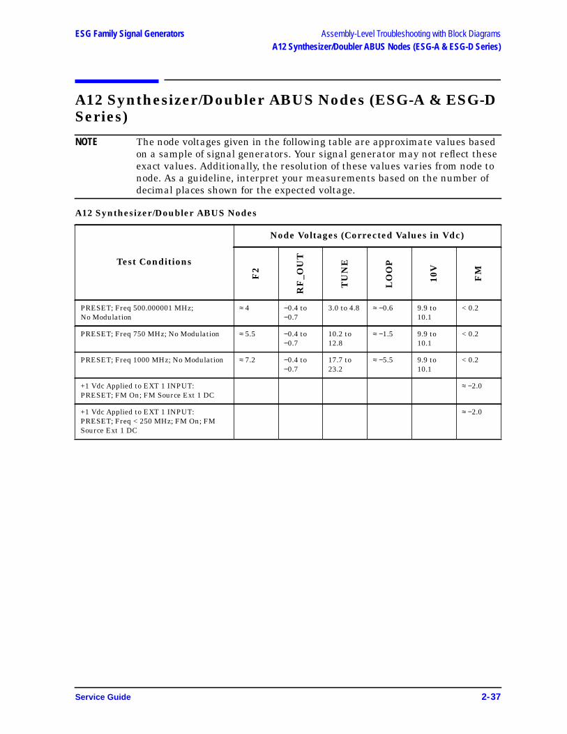
ESG Family Signal Generators Assembly-Level Troubleshooting with Block DiagramsA12 Synthesizer/Doubler ABUS Nodes (ESG-A & ESG-D Series)
A12 Synthesizer/Doubler ABUS Nodes (ESG-A & ESG-DSeries)
NOTE The node voltages given in the following table are approximate values basedon a sample of signal generators. Your signal generator may not reflect theseexact values. Additionally, the resolution of these values varies from node tonode. As a guideline, interpret your measurements based on the number ofdecimal places shown for the expected voltage.
A12 Synthesizer/Doubler ABUS Nodes
Test Conditions
Node Voltages (Corrected Values in Vdc)
F2
RF
_OU
T
TU
NE
LO
OP
10V
FM
PRESET; Freq 500.000001 MHz;No Modulation
≈ 4 −0.4 to−0.7
3.0 to 4.8 ≈ −0.6 9.9 to10.1
< 0.2
PRESET; Freq 750 MHz; No Modulation ≈ 5.5 −0.4 to−0.7
10.2 to12.8
≈ −1.5 9.9 to10.1
< 0.2
PRESET; Freq 1000 MHz; No Modulation ≈ 7.2 −0.4 to−0.7
17.7 to23.2
≈ −5.5 9.9 to10.1
< 0.2
+1 Vdc Applied to EXT 1 INPUT:PRESET; FM On; FM Source Ext 1 DC
≈ −2.0
+1 Vdc Applied to EXT 1 INPUT:PRESET; Freq < 250 MHz; FM On; FMSource Ext 1 DC
≈ −2.0
Service Guide 2-37
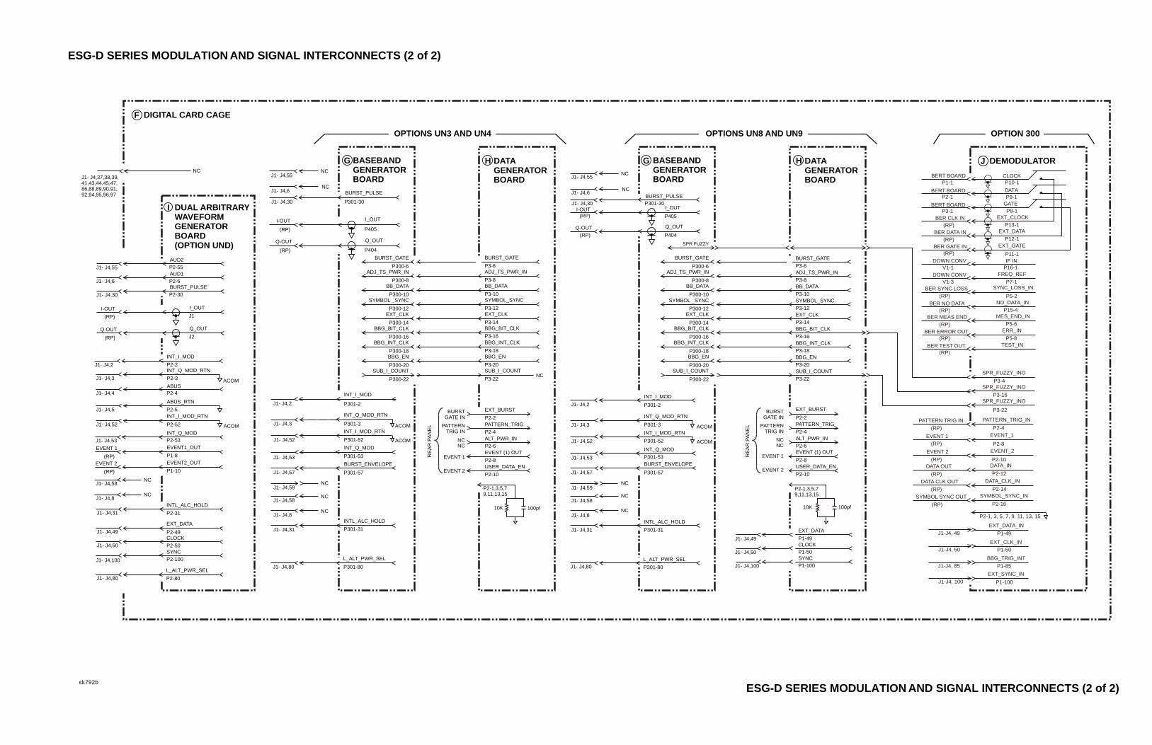
ESG-D SERIES MODULATION AND SIGNAL INTERCONNECTS (2 of 2)
BURST_PULSE
P301-30
NC
NC
J1- J4,55
J1- J4,6
J1- J4,30
RATORD
_IN
C
TNC
IG
T
EN
100pf
DATAGENERATORBOARD
HBASEBANDGENERATORBOARD
G
OPTIONS UN8 AND UN9
EXT_DATA
P1-49CLOCK
P1-50SYNC
P1-100
J1- J4,49
J1- J4,50
J1- J4,100
BURST_GATE
P3-6
ADJ_TS_PWR_IN
BB_DATA
SYMBOL_SYNC
EXT_CLK
BBG_BIT_CLK
BBG_INT_CLK
BBG_EN
SUB_I_COUNT
P3-8
P3-10
P3-12
P3-14
P3-16
P3-18
P3-20
P3-22
EXT_BURST
PATTERN_TRIG
ALT_PWR_IN
EVENT (1) OUT
USER_DATA_EN
P2-2
P2-4
P2-6
P2-8
P2-10
P2-1,3,5,79,11,13,15
10K 100pf
P301-3
P301-52
J1- J4,3
J1- J4,52
J1- J4,53
J1- J4,57
J1- J4,59
INT_Q_MOD_RTN
INT_Q_MOD
INT_I_MOD_RTN
P301-53
BURST_ENVELOPE
P301-57
ACOM
ACOM
NC
NC
NC
INTL_ALC_HOLD
P301-31
L_ALT_PWR_SEL
P301-80
J1- J4,58
J1- J4,8
J1- J4,31
J1- J4,80
INT_I_MOD
P301-2J1- J4,2
BURST_GATE
P300-6ADJ_TS_PWR_IN
BB_DATA
SYMBOL _SYNC
P300-8
P300-10
P300-12
BBG_INT_CLK
BBG_EN
SUB_I_COUNT
P300-18
P300-20
P300-22
EXT_CLK
BBG_BIT_CLKP300-14
P300-16
Q_OUTQ-OUT
I_OUTI-OUT
P404
P405(RP)
(RP)
NCNC
EVENT 1
EVENT 2
BURSTGATE IN
PATTERNTRIG IN
RE
AR
PA
NE
L
OPTION 300
DEMODULATORJ
SPR FUZZY
DOWN CONV
V1-1 P16-1
IF IN
DOWN CONV
V1-3 P7-1
FREQ_REF
(RP)
BER SYNC LOSS
P5-2
SYNC_LOSS_IN
(RP)
BER NO DATAP15-4
NO_DATA_IN
(RP)
BER MEAS END
P5-6
MES_END_IN
(RP)BER ERROR OUT
P5-8
ERR_IN
(RP)
BER TEST OUT TEST_IN
BERT BOARDP2-1 P9-1
DATA
BERT BOARD
P1-1
CLOCKP10-1
BERT BOARDP3-1 P8-1
GATE
BER CLK IN
(RP) P13-1
EXT_CLOCK
(RP)
BER DATA IN
P12-1
EXT_DATA
(RP)
BER GATE IN
P11-1
EXT_GATE
SPR_FUZZY_INO
P3-4SPR_FUZZY_INO
P3-16SPR_FUZZY_INO
P3-22
P2-4
PATTERN TRIG IN PATTERN_TRIG_IN
(RP)
EVENT 1 EVENT_1
(RP) P2-8
EVENT 2 EVENT_2
(RP) P2-10
DATA OUT DATA_IN
(RP) P2-12
DATA CLK OUT DATA_CLK_IN
(RP) P2-14
SYMBOL SYNC OUT SYMBOL_SYNC_IN
(RP) P2-16
J1-J4, 49
EXT_DATA_IN
P1-49
J1-J4, 50
EXT_CLK_IN
P1-50
J1-J4, 85
BBG_TRIG_INT
P1-85
J1-J4, 100
EXT_SYNC_IN
P1-100
P2-1, 3, 5, 7, 9, 11, 13, 15
sk792b
DIGITAL CARD CAGE F
J1- J4,37,38,39,41,43,44,45,47,86,88,89,90,91,92,94,95,96,97
NC
BURST_PULSE
AUD1
AUD2
P2-30
P2-6
P2-55J1- J4,55
J1- J4,6
J1- J4,30
DUAL ARBITRARYWAVEFORMGENERATORBOARD(OPTION UND)
I
Q_OUTQ-OUT
I_OUTI-OUT
J2
J1(RP)
(RP)
P2-52J1- J4,52
INT_I_MOD_RTN
EVENT1_OUT
EVENT2_OUT(RP)
(RP)
EVENT 1
EVENT 2
P1-8
P1-10
ACOM
J1- J4,53
INT_Q_MOD
P2-53
J1- J4,4
ABUS
P2-4
J1- J4,5
ABUS_RTN
P2-5
NC
NC
J1- J4,58
J1- J4,8
INTL_ALC_HOLD
P2-31J1- J4,31
L_ALT_PWR_SEL
P2-80J1- J4,80
P2-3J1- J4,3
INT_Q_MOD_RTN
ACOM
INT_I_MOD
P2-2J1- J4,2
EXT_DATA
P2-49J1- J4,49CLOCK
P2-50J1- J4,50
SYNC
P2-100J1- J4,100
DATAGENEBOAR
H
OPTIONS UN3 AND UN4
BURST_GATE
P3-6ADJ_TS_PWR
BB_DATA
SYMBOL_SYN
EXT_CLK
BBG_BIT_CLK
BBG_INT_CLK
BBG_EN
SUB_I_COUN
P3-8
P3-10
P3-12
P3-14
P3-16
P3-18
P3-20
P3-22
NCNC
EVENT 1
EVENT 2
BURSTGATE IN
PATTERNTRIG IN
EXT_BURST
PATTERN_TR
ALT_PWR_IN
EVENT (1) OU
USER_DATA_
P2-2
P2-4
P2-6
P2-8
P2-10
P2-1,3,5,79,11,13,15
10K
RE
AR
PA
NE
L
BASEBANDGENERATORBOARD
G
P301-3
P301-52
J1- J4,3
J1- J4,52
J1- J4,53
J1- J4,57
J1- J4,59
INT_Q_MOD_RTN
INT_Q_MOD
INT_I_MOD_RTN
P301-53
BURST_ENVELOPE
P301-57
ACOM
ACOM
NC
NC
NC
INTL_ALC_HOLD
P301-31
L_ALT_PWR_SEL
P301-80
J1- J4,58
J1- J4,8
J1- J4,31
J1- J4,80
INT_I_MOD
P301-2J1- J4,2
BURST_GATE
P300-6ADJ_TS_PWR_IN
BB_DATA
SYMBOL _SYNC
P300-8
P300-10
P300-12
BBG_INT_CLK
BBG_EN
SUB_I_COUNT
P300-18
P300-20
P300-22
EXT_CLK
BBG_BIT_CLKP300-14
P300-16
BURST_PULSE
P301-30
NC
NC
J1- J4,55
J1- J4,6
J1- J4,30
Q_OUTQ-OUT
I_OUTI-OUT
P404
P405(RP)
(RP)
ESG-D SERIES MODULATION AND SIGNAL INTERCONNECTS (2 of 2)

ESG Family Signal Generators Assembly-Level Troubleshooting with Block DiagramsA14 CPU/Motherboard ABUS Nodes
A14 CPU/Motherboard ABUS Nodes
NOTE The node voltages given in the following table are approximate values basedon a sample of signal generators. Your signal generator may not reflect theseexact values. Additionally, the resolution of these values varies from node tonode. As a guideline, interpret your measurements based on the number ofdecimal places shown for the expected voltage.
A14 CPU/Motherboard ABUS Nodes
Test Conditions
Node Voltages (Corrected Values in Vdc)
DIS
P
LC
D
INT
_MO
D
P10
V_R
EF
M6V
M5V
P9V
AC
OM
PRESET; ≈ 7a
a. Approximately −5.3 V if jumpers for P104, P105, and P106 are set to negative position.
0.00 10 −6.0 −5.2 9.0 0.00
PRESET; Vary Display Brightness 1 to50
−0.4 to−1.3
Service Guide 2-41

MEMORY SERIAL INTERFACE(INTERNAL)
INTERNALDATA BUS
SERIAL I/OBUS
SERIAL I/O
INTERFACE
L SERIALI/O INT
A14 CPU/MOTHERBOARD BLOCK DIAGRAM (1 OF 2)
FROINTE
INT CONTBUS
MEM ADDRBUS
MEM DATABUS
INT ADDRBUS
INTERNAL DATABUS
FLASHMEMORY1M X 32
EEROM64K X 8
NONVOLATILERAM128K X 16
RAM512 X 16
MEM ADDRBUS
MEM ADDRBUS
MEM ADDRBUS
MEM ADDRBUS
MEM DATABUS
MEM DATABUS
MEM DATABUS
MEM DATABUS
ATTEN ENABLE
ATTEN CLK
ATTEN DATA
ATTENUATOR & RPP INTERFACE
TO: DAUGHTERBOARD
L DCC ALT
PWR SEL
TRIG INT
INTERNAL DATA BUS
HFATTENCONTROL
ATTENSENSE
L RPP INT
L RPP RESET
RFACE
TERNALATA BUS
T ADDRUS
HP-IBINTERFACE
TO: HP-IB
DIGITAL SIGNAL PROCESSOR (DSP)
ABUS
INT MODINTERNAL MODULATION DAC
DSP TRIG OUT
L DSP INT
CLK OUT
RESET
TRIG INT
INT ADDR BUS
DSP ADDR BUS
DSP DATA BUSINTERNAL DATA BUS
16 MHzCLOCK
DSP/CPUINTERFACE
DIGITALSIGNALPROCESSOR
SERIAL INTERFACE
DSP ADDR BUS
DSP RAM
DSP DATA BUS
DSPRAM32K X 8
+
TP705TP706
TO: DAUGHTERBOARD
ANALOG TO DIGITAL CONVERTER (ADC)
SWEEP RAMP
SERIAL INTERFACE
+
SWEEPOUT
J9
+10V REF
SWEEP RAMP
A BUS
BUF ABUSBUF ABUS
ABUS
ABUS RTN
TP703
TP702
ADC INTP704 +5V
ADC
INT_I_MOD
INT_I_MOD
P102
P103
EXT. DATA & CLOCK IN
P5
P6
P7
JI-49J2-49J3-49J4-49
JI-50J2-50J3-50J4-50
JI-100J2-100J3-100J4-100
DATA
CLOCK
SYMB_SYNC
MECH.ELEC.
REF ENABLE
REF CLK
REF DATA
SYNTH ENABLE
SNTH CLK
SYNTH DATA
OUTPUT ENABLE
OUTPUT CLK
OUTPUT DATA
INT_I_MOD1
INT_Q_MOD1
SPARE_I_DATA
SPARE_I_EN
J18
2
3
4
7
8
TO PULSEMODULATOROPTION 1E6
LATN
LEOI
LSRQ
LREN
LIFC
LDAV
NDAC
NRFD
DIO1
DIO2
DIO3
DIO4
DIO5
DIO6
DIO7
DIO8
J7-11
J7-5
J7-10
J7-17
J7-9
J7-6
J7-8
J7-7
J7-1
J7-2
J7-3
J7-4
J7-13
J7-14
J7-15
J7-16
+15V
+12.5V
+5.2V
-12.5V
ACOM
L = LF ATTEN
L=HF ATTEN
ATTEN_405_5
ATTEN_5A_10
ATTEN_10A_40
ATEN XX
ATTEN_20_XX
ATTEN_10B_20
ATTEN_40A_60
ATTEN_5B_XX
J14-17
J14-11
J14-10
J14-9
J14-7
J14-6
J14-5
J14-4
J14-3
J14-2
ATTEN ENABLE
ATTEN CLK
ATTEN DATA
L RPP INT
L RPP RESET
J14-20
J14-19
J14-18
J14-16
J15-2
J14-12
J15-1
J14-1
J14-14
J15-3
J14-15
J15-5
J14-13
J15-4
J14-8
-15V
+5.2VD
J5-24
J5-45
J5-44
J5-70
J5-73
J5-76
J5-20
J5-23
J5-26
J5-18
J5-21
TRIGGER I/O
DSP TRIG OUT
CPU TRIG INTDCC TRIG INTTRIG INT
TRIGENABLE
TRIGENABLE
TRIGGERIN
J11
TRIGGER
OUT
J10
10 MHz IN/OUT
10 MHzOUT
10 MHz
IN
J12
J13
FROM:DAUGHTERBOARD
TO:DAUGHTERBOARD
CPU TRIG OUT
DCC TRIG OUT
TP701
DAC
DAC
SWITCH & LEDS
INTERNALDATA BUS
SELF TESTLEDS
CONFIGSWITCH
INT ADDRBUS
CPU CLOCK
CPU INTERFACE
CPU
SERIAL INTERFACE(EXTERNAL)
32.77 kHzCLOCK
RS-232SERIALINTERFACE
+5V
J8-2
J8-8
J8-3
J8-7
J8-4
J8-5
RECV
CTS
XMIT
RTS
+5V
RXD
TXD
L PRESET
L HALT
M: AUXILIARYRFACE
ADDRESSBUFFERS
DATABUFFERS
BUSCONTROL
BOOTROM
ADDRESS BUS
CPU DATA BUS
SERIAL I/O BUS
CPU DATA BUS
HP- IB INTE
IND
INB
L HP-IB INT
FLASH PROGRAMVOLTAGE
INTERNALDATA BUS
ENABLEFLASHPROGRAM
VOLTAGEREG+15V FLASH
VPP
TP303
PROGRAM = +12V
IRQ1IRQ2IRQ3IRQ4
IRQ7IRQ6IRQ5
TP CLKTPU0
TPU1TPU2
TPU3TPU4TPU5TPU6TPU7TPU8
TPU10
L SERIAL I/O INTNOT USEDL HP-IB INTL RPG INT
NOT USED
L KEY INT
NOT USED
10 MHz DIGCOUNTER
CPU TRIG INTL DSP INT
DIG BUS INT 1DIG BUS INT 2DIG BUS INT 3DIG BUS INT 4
PULSE INTL RPP INT
CTS
sk789b A14 CPU/MOTHERBOARD BLOCK DIAGRAM (1 0F 2)

A14 CPU/MOTHERBOARD BLOCK DIAGRAM (2 OF 2)
RPG
DECODER
RPG A
RPG B
L RPG INT
TO RPG
INTERNAL DATA BUS
J20-12+5V
ODER
TO FRONT PANEL
KEYROW 0
KEYROW 1
KEYROW 2
KEYROW 3
KEYROW 4
INTERNAL DATA BUS
KEYROW 5
KEYROW 6
KEYROW 7
J20-17
J20-19
J20-21
J20-23
J20-25
J20-26
J20-24
J2-22
D DECODER
NT PANEL
KEYCOL 0
KEYCOL 1
KEYCOL 2
KEYCOL 3
KEYCOL 4
KEYCOL 5
KEYCOL 6
KEYCOL 7
L KEY INT
KEYBOARD
COLUMN
DECODERINTERNAL DATA BUS
KEYBOARD
ROW
LATCH
DIGITAL CARD CAGE CONNECTIONS DAUGHTER BOARD CONNECTIONS
POWER SUPPLY DIAGNOSTICS
POWER
SUPPLY
DIAGNOSTICS
+32V
+15V
+12V
-15V
+5.2VD
DS503-A
LOW=+32V OK
LOW=+15V OK
LOW=+12V OK
LOW=-15V OK
+5.2VD
DS503-E DS503-B DS503-DDS503-C
JUMPER ACROSS
PINS TO RESET
J29-2
J29-1
SENSE
LOW RESET
POWER RESET
POWER
RESET
+5.2VD
+5.2VDL PRESET
L HALT
L STANDBY
FAN POWER SUPPLY
+12V
+12V
FAN+
FAN+
J16-1
J16-2
J17-1
J17-2
NONVOLATILE MEMORY POWER
V BAT
SELECT+5.2VD
+5.1V
+3V
BT1
+15V STANDBY
VBAT
SERIAL I/O SIGNALS
POWER SUPPLIES
MNEMONIC J5
18
21
24
20
23
26
70
73
76
REF DATA
REF CLK
REF ENABLE
SYNTH DATA
SYNTH CLK
SYNTH ENABLE
OUTPUT DATA
OUTPUT CLK
OUTPUT ENABLE
MNEMONIC J5
83
32,82
33
34,84
30,31
80,81
35,85
37,87
36,86
4,10
16,22
28,51
57,63
69,75
43,47
49,96
+32V
+15V
+15V STBY
+9V
+5.2V
-5.2V
-6V
-15V
DCOM
ACOM
MNEMONIC J5
40
97
99
98,100
93
92
91
17
29
48
46
42
79
15
41
55
60
56
11
5
61
62
6
12
7
13
14
59
8
64
58
50
44
45,94
95
54
9
3
53
2
+PTAT
10 MHz IN
10 MHz OUT
10 MHz RTN
ABUS
ABUS RTN
ALC GND
L ALC HOLD
L ALT PWR SEL
AUD 1 (NOT USED)
AUD 2 (NOT USED)
BURST ENVELOPE
BURST PULSE
COUNTER
FADE ENVELOPE
FM D0
FM D1
FM D2
FM D3
FM D4
FM D5
FM D6
FM D7
FM D8
FM D9
FM D10
FM D11
FM D12
FM D13
FM D14
FM D15
INT MOD
INT I MOD
INT I/Q MOD RTN
INT Q MOD
MOD STROB
PAREN SYNC
SWP READY
SWP STATUS
SWP RUN
CPU INTERFACE
MNEMONIC J1 J2 J3 J4
24
74 74 74 74
25 25 25 25
26 26 26 26
76 76 76 76
27 27 27 27
77 77 77 77
78 78 78 78
29 29 29 29
79 79 79 79
36 36 36 36
24 24 24IAB0
IAB1
IAB2
IAB3
IAB4
IAB5
IAB6
IAB7
IAB8
IAB9
IAB10
19 19 19 19
20 20 20 20
70 70 70 70
21 21 21 21
71 71 71 71
72 72 72 72
23 23 23 23
73 73 73 73
EXT D0
EXT D1
EXT D2
EXT D3
EXT D4
EXT D5
EXT D6
EXT D7
32
83
82
33
33
33
33
EXT RESET
EXT RD L WR
EXT L STROBE
EXT SELECT 1
EXT SELECT 2
EXT SELECT 3
EXT SELECT 4
INT ADDR BUS
INT DATA BUS
CONTROL BUS
POWER SUPPLIES
CPU INTERFACE
MNEMONIC J1 J2 J3 J4
9 9 9 9
14,64 14,64 14,64 14,64
15,65 15,65 15,65 15,65
16,17 16,17 16,17 16,17
66,67 66,67 66,67 66,67
12,62 12,62 12,62 12,62
13,63 13,63 13,63 13,63
22,28 22,28 22,28 22,28
34,40 34,40 34,40 34,40
46,69 46,69 46,69 46,69
75,81 75,81 75,81 75,81
87,93 87,93 87,93 87,93
99 99 99 99
1,7 1,7 1,7 1,7
54,56 54,56 54,56 54,56
+32V
+15V
+12V
+5.2V
-5.2V
-15V
DCOM
ACOM
35
35
35
35
DIG BUS INT 1
DIG BUS INT 2
DIG BUS INT 3
DIG BUS INT 4
MNEMONIC J1 J2 J3 J4
59 59 59 59
84 84 84 84
4 4 4 4
5 5 5 5
8 8 8 8
31 31 31 31
6 6 6 6
55 55 55 55
57 57 57 57
30 30 30 30
86 86 86 86
80 80 80 80
18 18 18 18
85 85 85 85
58 58 58 58
47 47 47 47
91 91 91 91
95 95 95 95
90 90 90 90
96 96 96 96
41 41 41 41
89 89 89 89
45 45 45 45
39 39 39 39
94 94 94 94
88 88 88 88
37 37 37 37
92 92 92 92
43 43 43 43
38 38 38 38
44 44 44 44
2 2 2 2
3,52 3,52 3,52 3,52
53 53 53 53
97 97 97 97
42 42 42 42
48 48 48 48
98 98 98 98
49 49 49 49
+PTAT
10 MHz DIG
ABUS
ABUS RTN
ALC GND
L ALC HOLD
AUD 1 (NOT USED)
AUD 2 (NOT USED)
BURST ENVELOPE
BURST PULSE
COUNTER
L DCC ALT PWR SEL
DCC TRIG OUT
DCC TRIG INT
FADE ENVELOPE
FM D0
FM D1
FM D2
FM D3
FM D4
FM D5
FM D6
FM D7
FM D8
FM D9
FM D10
FM D11
FM D12
FM D13
FM D14
FM D15
INT I MOD
INT I/Q MOD RTN
INT Q MOD
MOD STROB
PAREN SYNC
SWP READY
SWP STATUS
SWP RUN
SWITCHING POWER SUPPLIES
ABUS
ABUS
NEGATIVE
SWITCHING
SUPPLIES
+5.2VD -5.2V
M5V
M6V
DS503-H
TP509
TP508
-6V
DS503-G
TP504
SWITCHING
SUPPLY+12V +32V
TP502
TP502
TP506
TP502
SUPPLY
FILTERING
+15V STANDBY
+15V
-15V
+12V
+5.2V+5.2VD
+5.2V
J6-17
J6-20
J6-18
J6-19
J6-2,3,
12,13
+15V STBY
+15V
DS502
DS502
-15V
+12V
FROM POWER SUPPLY
POWER SUPPLY INPUTS POWER SUPPLY REGULATORS
TP510
+12.5V
REG+15V +12.5V
DS504
TP501
+10V
REG+15V +10VREF
P10V_REF
TP507
+9V
REG+10VREF +9V
P9V
DS504
ABUS
ABUS
TP511
-12.5V
REG-15V +12.5V
DS505
L PWRONJ6-1TO PWR SUPPLY
TO: FRONT
PANEL
POWER
SWITCH
LATCH
ON/OFF SW
PANEL
PWR GREENJ20-2
J20-4STBY YELLOW
+15V STBY
N
ABUS
VDISP
LCD BRIGHTNESS DRIVER(FLUORESCENT)
INTERNAL DATA BUS
+
TP601
TO: LCD
J19-1
J19-2
J19-3
+5V
+10 VREF
OPEN=
DISPLAY ENABLED
+5V
LCD CONTROLLER
DISPLAY
ENABLEJ21-4
+5V J21-5
SHIFT
CLOCKJ21-3
TO LCD DISPLAYFLM
LP
P0
P1
P2
P3
P4
P5
P6
P7
J21-1
J21-2
J21-11
J21-10
J21-9
J21-8
J21-15
J21-14
J21-13
J21-12
LCD RAM INTERFACELCD RAM
256K X 16
RESET
LCD DATA BUS
MEM ADDR BUS
CPU DATA BUS
14.32 MHz
CLOCK
LCD DATA
BUFFER
LCD
CONTROLLER
J20-14
J20-10
FROM RPG
RPG DEC
KEYBOAR
FROM FRO
J20-1
J20-3
J20-5
J20-7
J20-9
J20-11
J20-13
J20-15
DAC
LCD DRIVER VOLTAGE(CONTRAST)
INTERNAL DATA BUS
TO: LCD
ABUS
VLCD
TP602
J21-7
VARIABLE
POWER
SUPPLY
+10 VREF
CLOSED=
DISPLAY ENABLED
DAC
J20-20
FROM FRONT
POWER OPOLARITY
CONTROL JUMPERS
P104, 5, 6
A14 CPU/MOTHERBOARD BLOCK DIAGRAM (2 OF 2)sk790b

ESG Family Signal Generators Assembly-Level Troubleshooting with Block DiagramsA20 Downconvertor Block Diagram (Option 300)
A20 Downconvertor Block Diagram (Option 300)
Service Guide 2-47
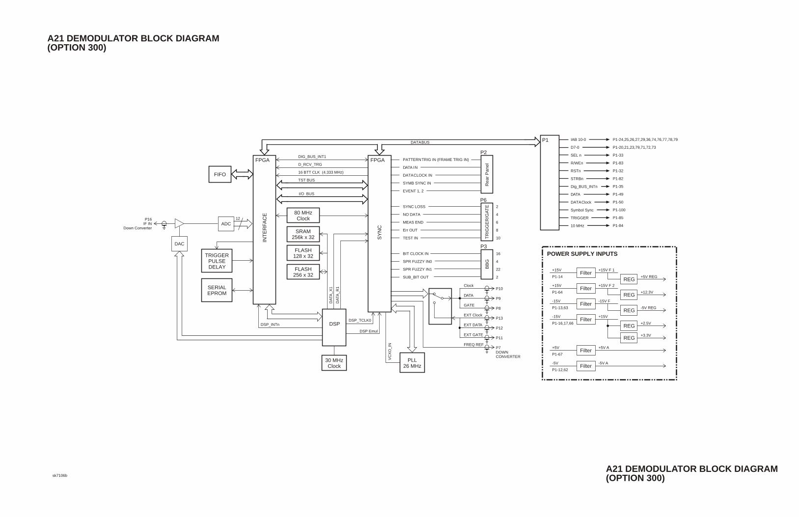
A21 DEMODULATOR BLOCK DIAGRAM
A21 DEMODULATOR BLOCK DIAGRAM
POWER SUPPLY INPUTS
+15V F 1Filter
+5V REGREG
+15V F 2Filter
+12.3VREG
-15V FFilter
-5V REGREG
+15VFilter
+2.5VREG
+3.3VREG
+5V AFilter
-5V A
+15V
P1-14
+15V
P1-64
-15V
P1-13,63
-15V
P1-16,17,66
+5V
P1-67
-5V
P1-12,62Filter
IAB 10-0
D7-0
SEL n
R/WEn
RSTn
STRBn
Dig_BUS_INTn
DATA
DATA Clock
Symbol Sync
TRIGGER
10 MHz
P1-24,25,26,27,29,36,74,76,77,78,79
P1-20,21,23,79,71,72,73
P1-33
P1-83
P1-32
P1-82
P1-35
P1-49
P1-50
P1-100
P1-85
P1-84
P1
PATTERN TRIG IN (FRAME TRIG IN)
DATA IN
DATA CLOCK IN
SYMB SYNC IN
EVENT 1, 2
SYNC LOSS
NO DATA
MEAS END
Err OUT
TEST IN
BIT CLOCK IN
SPR FUZZY IN0
SPR FUZZY IN1
SUB_BIT OUT
2
4
6
8
10
16
4
22
2
P2
TR
IGG
ER
/GA
TE
FPGA
SY
NC
Rear
Panel
BB
G
P6
P3
Clock
DATA
GATE
EXT Clock
EXT DATA
EXT GATE
FREQ REF
P10
P9
P8
P13
P12
P11
P7
PLL26 MHz
VC
XO
_IN
TCLK0
DSP Emul
DOWNCONVERTER
DATA BUS
(OPTION 300)
80 MHzClock
SRAM256k x 32
FLASH128 x 32
FLASH256 x 32
30 MHzClock
DIG_BUS_INT1
D_RCV_TRG
16 BTT CLK (4.333 MHz)
TST BUS
FPGA
INT
ER
FA
CE
DA
TA
_X
1
DA
TA
_R
1
DSPDSP_
DSP_INTn
I/O BUS
P16IF IN
Down Converter
12
ADC
DAC
TRIGGERPULSEDELAY
FIFO
SERIALEPROM
(OPTION 300)sk7106b

ESG Family Signal Generators Assembly-Level Troubleshooting with Block DiagramsA22 YIG Driver ABUS Nodes (ESG-AP & ESG-DP Series)
A22 YIG Driver ABUS Nodes(ESG-AP & ESG-DP Series)
NOTE The node voltages given in the following table are approximate values basedon a sample of signal generators. Your signal generator may not reflect theseexact values. Additionally, the resolution of these values varies from node tonode. As a guideline, interpret your measurements based on the number ofdecimal places shown for the expected voltage.
A22 YIG Driver ABUS Nodes (ESG-AP & ESG-DP Series)
Test Conditions:
PRESET; 0 dBm; RF On;No Modulation
Node Voltages(Corrected Values in Vdc)
FM
_DR
VR
PL
L_D
RV
R
N5V
PR
ET
UN
E(−
5.3
to 0
.1)
0 0 −5
Freq 0.25 MHz −4
Freq 750 MHz −3
Freq 1 GHz −4
Freq 1.001 GHz −2
Freq 2 GHz −4
Freq 2.5 GHz −2.5
Freq 4 GHz −4
Service Guide 2-51

FM COIL
MAINYTOCOIL
SPLITTER
6dB
6dB 9dB
8dB
+9dB
12GHZ
8dB
J7 TOFRAC- N/DIVIDER
J8 TO SAMPLER
FILTER
FILTER
FILTER
-+
ABUS
+5V
-15V
+15V
+5VREG Q1
-5VF
+5VF
-15VF
+15VF
-5VF
POWER SUPPLY
-15 VF
+5VF
TP4
+15VF
IO
CIK
DATA
EN
DATA
DATA
LATCH
LATCH
8
8
MUXFM DRIVERPLL TUNEPRETUNE
-5VF
ABUS
SERIALIO
CIKDATASELECT
s
EEPROM
SA
> +10dBm
» 0dBm
» 0dBm
P1-4
FM DRIVER
J30-66dB
6dB STEPS
DACADJ FREQCOMP
FIXED FREQCOMP
0-36dB12dB STEPS
0-6dB 0 - -2.2dB@10 MHz +5dB @ 10MHz
ABUS
FM DRIVER
TP1 FM
ABUS
PLL INTERFACE
J4
CROSSOVER
>230 Hz
<230Hz
PLL DRIVER
J1-5
J1-4,6
TP2
DAC
PRETUNE
+5VREF
ABUS
12 BIT
115Hz
PRETUNE
CURRENT SOURCE
-15VF
J1-8, 9
J1-7, 10
J1-1J1-2J1-3
+15-5
GND
TP3
J6
A22 YIG DRIVER BLOCK DIAGRAM
k768b
FM INFROM
FRAC-N/DIVIDER
FROMMPLER
YTO
A22 YIG DRIVER BLOCK DIAGRAM
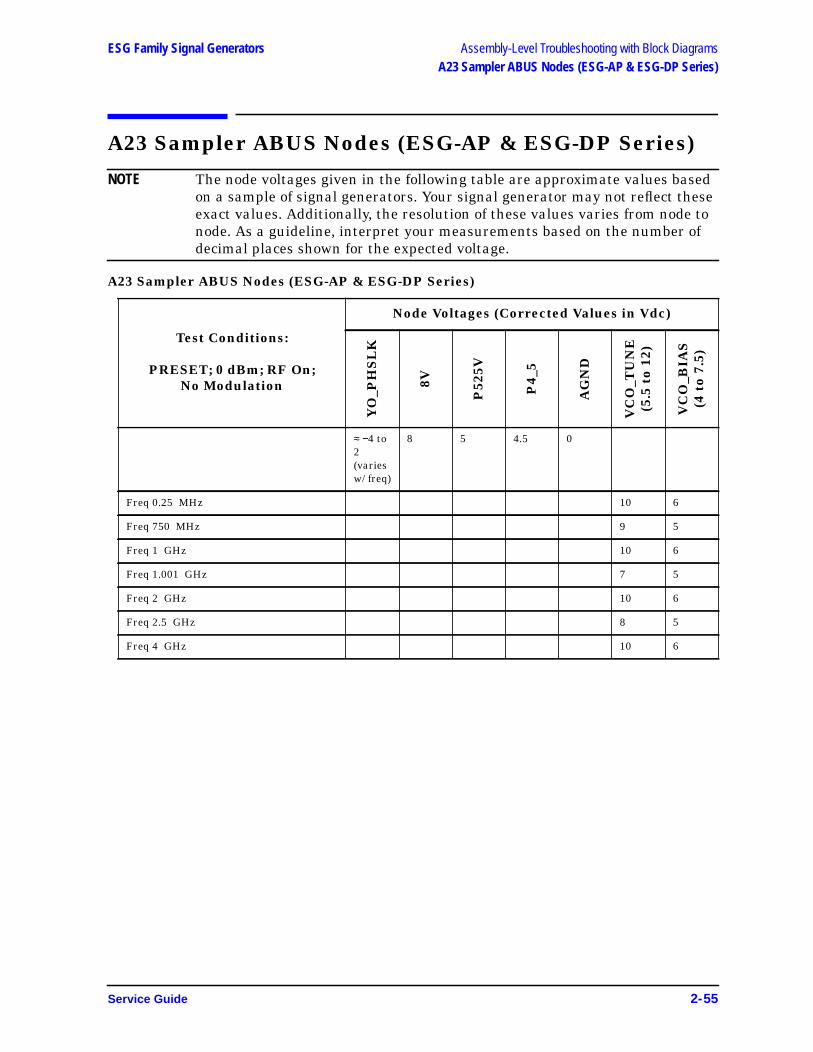
ESG Family Signal Generators Assembly-Level Troubleshooting with Block DiagramsA23 Sampler ABUS Nodes (ESG-AP & ESG-DP Series)
A23 Sampler ABUS Nodes (ESG-AP & ESG-DP Series)
NOTE The node voltages given in the following table are approximate values basedon a sample of signal generators. Your signal generator may not reflect theseexact values. Additionally, the resolution of these values varies from node tonode. As a guideline, interpret your measurements based on the number ofdecimal places shown for the expected voltage.
A23 Sampler ABUS Nodes (ESG-AP & ESG-DP Series)
Test Conditions:
PRESET; 0 dBm; RF On;No Modulation
Node Voltages (Corrected Values in Vdc)
YO
_PH
SL
K
8V
P52
5V
P4_
5
AG
ND
VC
O_T
UN
E(5
.5 t
o 12
)
VC
O_B
IAS
(4 t
o 7.
5)
≈ −4 to2(variesw/ freq)
8 5 4.5 0
Freq 0.25 MHz 10 6
Freq 750 MHz 9 5
Freq 1 GHz 10 6
Freq 1.001 GHz 7 5
Freq 2 GHz 10 6
Freq 2.5 GHz 8 5
Freq 4 GHz 10 6
Service Guide 2-55
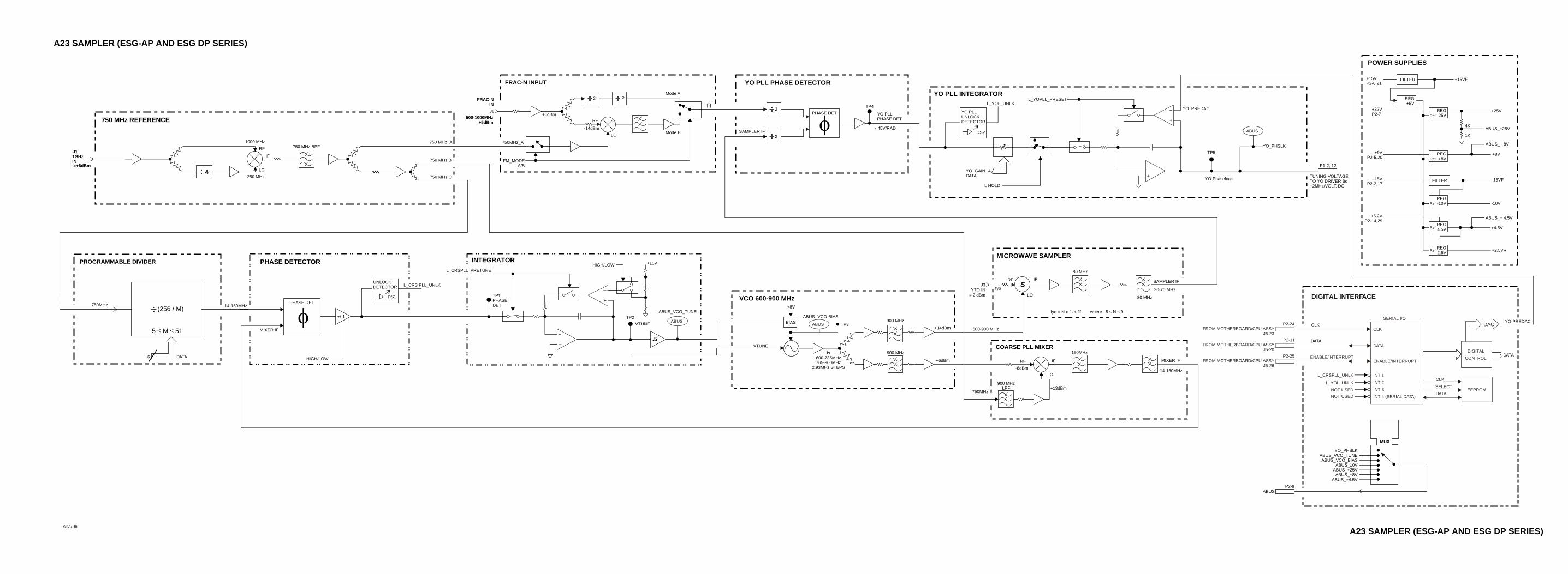
A23 SAMPLER (ESG-AP AND ESG DP SERIES)
750 MHz A
750 MHz B
14-150MHz
IF
LO
L_CRS PLL_UNLK
MICROWAVE SAMPLER
SSJ3YTO IN
» 2 dBm
fyo
RF IF
LO
fyo = N x fs + fif
SAMPLER IF
30-70 MHz
where 5 £ N £ 9
80 MHz
80 MHzVCO 600-900 MHz
ABUS
+8V
fs600-735MHz765-900MHz
2.93MHz STEPS
+14dBm
+6dBm
900 MHz
900 MHz
BIAS
ABUS- VCO-BIAS
TP3
VTUNE COARSE PLL MIXER
750MHz
600-900 MHz
+13dBm
RF
-8dBm
MIXER IF
900 MHzLPF
FRAC-N INPUT
2 P
J6
FRAC-NIN
500-1000MHz+5dBm
750MHz_A
FM_MODE A/B
+6dBm
RF
-14dBm
LO
fif
Mode A
Mode B
2
YO PLL PHASE DETECTOR
SAMPLER IF
PHASE DET
TP4
YO PLL PHASE DET
-.45V/RADf2
POWER SUPPLIES
FILTER
FILTER
REG+5V
REG25V
REG+8V
REG4.5V
REG2.5V
REG-10V
Ref
Ref
Ref
Ref
Ref
+15VP2-6,21
+15VF
+32VP2-7
+25V
4K
1K
ABUS_+25V
ABUS_+ 8V
ABUS_+ 4.5V
+8V
-15VF
-10V
+4.5V
+2.5VR
+9VP2-5,20
-15VP2-2,17
+5.2VP2-14,29
YO PLL INTEGRATOR
YO PLLUNLOCKDETECTOR
DS2
4
L_YOL_UNLK
YO_GAINDATA
L HOLD
ABUS
YO_PHSLK
TP5
YO PhaselockTUNING VOLTAGETO YO DRIVER Bd+2MHz/VOLT. DC
P1-2, 12
+
_
+
_
L_YOPLL_PRESET
YO_PREDAC
150MHz
DIGITAL INTERFACE
FROM MOTHERBOARD/CPU ASSYJ5-26
FROM MOTHERBOARD/CPU ASSYJ5-20
FROM MOTHERBOARD/CPU ASSYJ5-23
SERIAL I/O
INT 1
INT 2
INT 3
INT 4 (SERIAL DATA)
CLK
ENABLE/INTERRUPT
CLK
DATA
ENABLE/INTERRUPT
L_CRSPLL_UNLK
L_YOL_UNLK
NOT USED
NOT USED
CLK
SELECT
DATAEEPROM
P2-24
P2-25
P2-11
DIGITAL
CONTROL
DATA
YO_PHSLKABUS_VCO_TUNEABUS_VCO_BIAS
ABUS_10VABUS_+25V
ABUS_+8VABUS_+4.5V
MUX
ABUSP2-9
DATA
DACYO-PREDAC
+
_
ABUS
ABUS_VCO_TUNE
TP2
.5.5
VTUNE
TP1PHASEDET
+
_
+15VHIGH/LOW
L_CRSPLL_PRETUNE
750 MHz C
INTEGRATOR
44
750 MHz REFERENCE
RF
LO
IF
750 MHz BPF1000 MHz
250 MHz
PROGRAMMABLE DIVIDER
(256 / M)
5 £ M £ 51
DATA6
750MHz 14-150MHz
PHASE DETECTOR
UNLOCKDETECTOR
DS1
PHASE DET
MIXER IF
HIGH/LOW
f
J11GHzIN
+6dBm
+/-1
sk770b
A23 SAMPLER (ESG-AP AND ESG DP SERIES)

ESG Family Signal Generators Assembly-Level Troubleshooting with Block DiagramsA24 Frac-N/Divider ABUS Nodes (ESG-AP & ESG-DP Series
A24 Frac-N/Divider ABUS Nodes (ESG-AP & ESG-DPSeries
NOTE The node voltages given in the following table are approximate values basedon a sample of signal generators. Your signal generator may not reflect theseexact values. Additionally, the resolution of these values varies from node tonode. As a guideline, interpret your measurements based on the number ofdecimal places shown for the expected voltage.
A24 Frac-N/Divider ABUS Nodes
Test Conditions:
PRESET; 0 dBm; RFOn; No Modulation
Node Voltages (Corrected Values in Vdc)
RF
_OU
T
10V
FM
M10
V
GN
D
F2
TU
NE
(3 t
o 23
)
LO
OP
(−10
to
0)
1 to 6 10 0.15 −10.0 0 −1 to −5typical
Freq 0.25 MHz 3.6 6
Freq 750 MHz 4 3 to 23
Freq 1 GHz 3.8 7
Freq 1.001 GHz 4.1 10
Freq 2 GHz 3.8 7
Freq 2.5 GHz 4.7 3 to 23
Freq 4 GHz 3.8 7
Service Guide 2-59
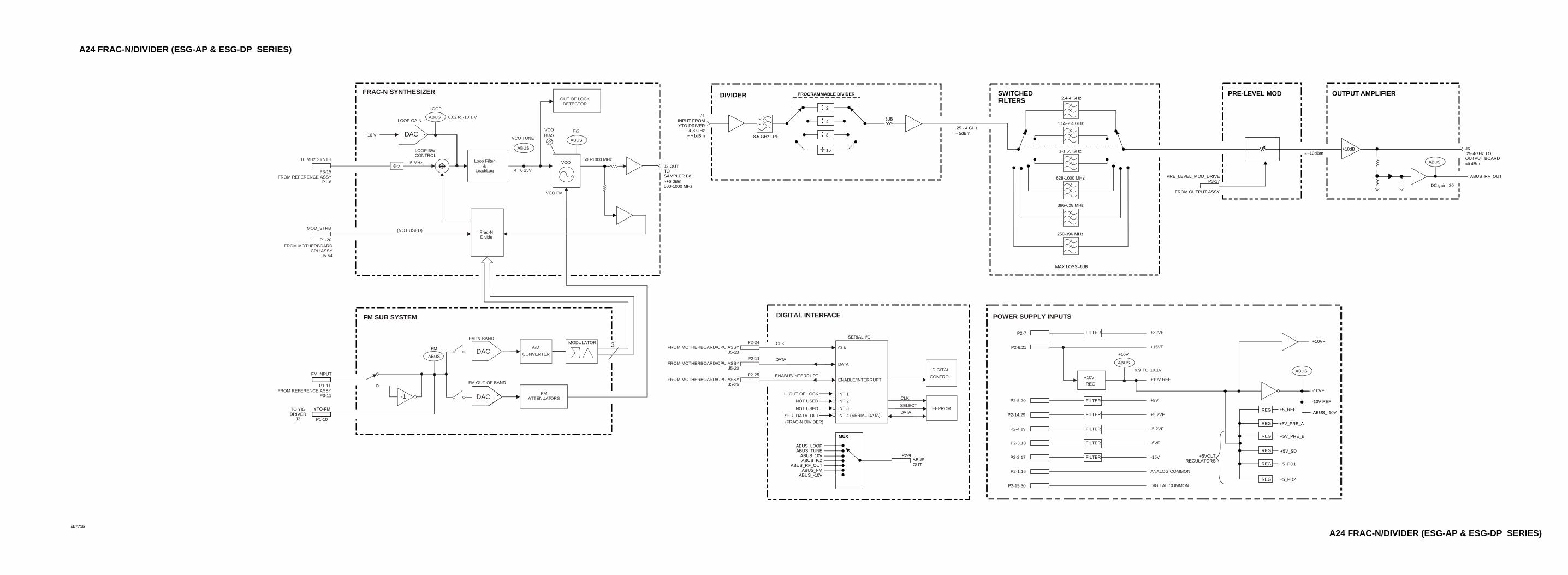
F
ABUS
ABUS
ABUS
VCO TUNE
4 T0 25V
500-1000 MHz
OOP GAIN
THESIZER
DAC
Loop Filter&
Lead/Lag
OUT OF LOCKDETECTOR
VCO
Frac-NDivide
5 MHz
LOOP
0.02 to -10.1 V
VCO FM
OT USED)
F/2VCO
BIAS
LOOP BWCONTROL
J2 OUTTOSAMPLER Bd.»+6 dBm500-1000 MHz
DIGITAL INTERFACE
FROM MOTHERBOARD/CPU ASSYJ5-26
FROM MOTHERBOARD/CPU ASSYJ5-20
FROM MOTHERBOARD/CPU ASSYJ5-23
SERIAL I/O
INT 1
INT 2
INT 3
INT 4 (SERIAL DATA)
CLK
ENABLE/INTERRUPT
CLK
DATA
ENABLE/INTERRUPT
L_OUT OF LOCK
NOT USED
NOT USED
SER_DATA_OUT
(FRAC-N DIVIDER)
CLK
SELECT
DATAEEPROM
P2-24
P2-25
P2-11
DIGITAL
CONTROL
DATA
ABUS_LOOPABUS_TUNE
ABUS_10VABUS_F/Z
ABUS_RF_OUTABUS_FM
ABUS_-10V
MUX
ABUSOUT
P2-9
ABUS
ABUS
POWER SUPPLY INPUTS
REG
+10V
P2-5,20
P2-14,29
P2-4,19
P2-3,18
P2-2,17
P2-1,16
P2-15,30
+15VF
+10V
9.9 TO 10.1V
+32VF
+10V REF
+9V
+5.2VF
-5.2VF
-6VF
-15V
ANALOG COMMON
DIGITAL COMMON
P2-7
P2-6,21
FILTER
FILTER
FILTER
FILTER
FILTER
FILTER
REG
REG
REG
REG
REG
REG
+5VOLTREGULATORS
+5_REF
+5V_PRE_A
+5V_PRE_B
+5V_SD
+5_PD1
+5_PD2
-10VF
+10VF
-10V REF
ABUS_-10V
ABUS
FM
DAC
DACA/D
CONVERTER
FMATTENUATORS
STEM
FM IN-BAND
FM OUT-OF BAND
3MODULATOR
DIVIDER
2
4
8
16
J1INPUT FROMYTO DRIVER
4-8 GHz» +1dBm
PROGRAMMABLE DIVIDER
.25 - 4 GHz» 5dBm
2.4-4 GHz
1.55-2.4 GHz
1-1.55 GHz
628-1000 MHz
396-628 MHz
250-396 MHz
MAX LOSS=6dB
SWITCHEDFILTERS
PRE-LEVEL MOD OUTPUT AMPLIFIER
PRE_LEVEL_MOD_DRIVEP3-17
» -10dBm+10dB
ABUS_RF_OUT
J6.25-4GHz TO OUTPUT BOARD»0 dBmABUS
FROM OUTPUT ASSY
3dB
8.5 GHz LPF
DC gain=20
-1
A24 FRAC-N/DIVIDER (ESG-AP & ESG-DP SERIES)
sk771b
L
FRAC-N SYN
+10 V
2
(N
10 MHz SYNTH
P3-15FROM REFERENCE ASSY
P1-6
MOD_STRB
P1-20
FROM MOTHERBOARDCPU ASSY
J5-54
FM SUB SY
FM INPUT
P1-11FROM REFERENCE ASSY
P3-11
YTO-FM
P1-10
TO YIGDRIVER
J3
A24 FRAC-N/DIVIDER (ESG-AP & ESG-DP SERIES)

ESG Family Signal Generators Assembly-Level Troubleshooting with Block DiagramsAT1 Electronic Attenuator/RPP Block Diagram
AT1 Electronic Attenuator/RPP Block Diagram
Service Guide 2-63

ESG Family Signal Generators Assembly-Level Troubleshooting with Block DiagramsAT1 Mechanical Attenuator and A19 RPP Block Diagram (Option UNB)
AT1 Mechanical Attenuator and A19 RPP BlockDiagram (Option UNB)
Service Guide 2-65
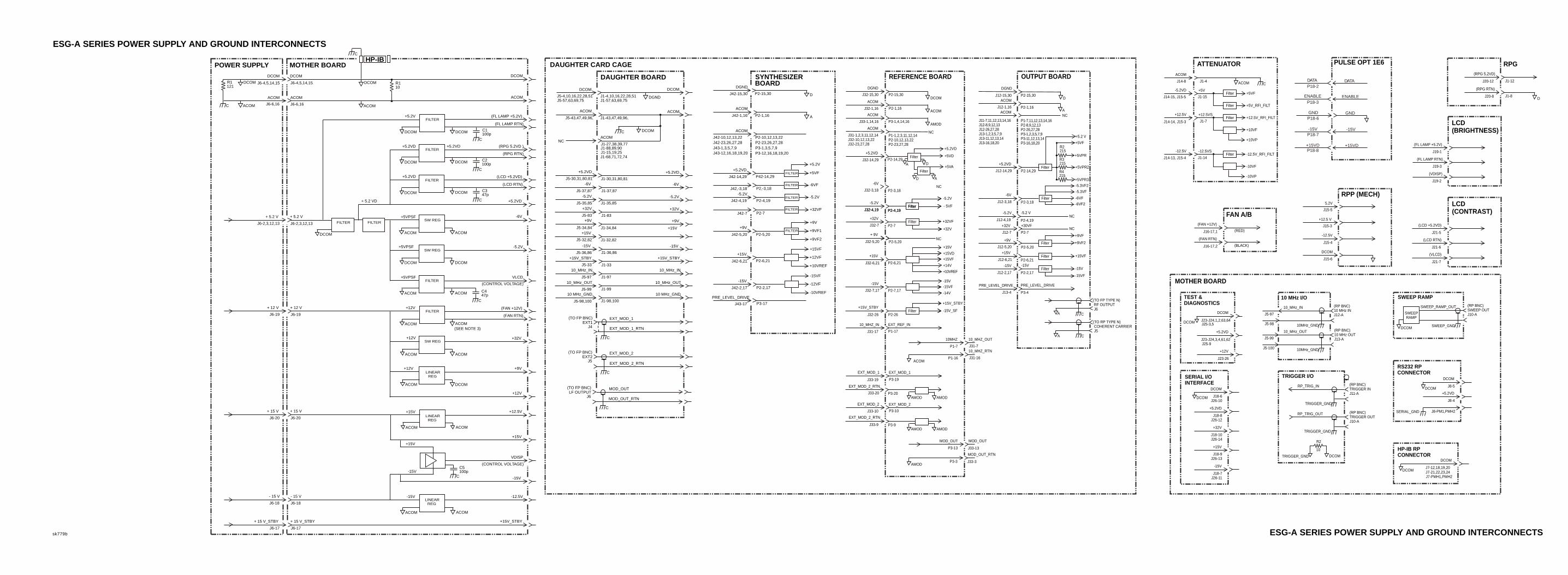
ESG-A SERIES POWER SUPPLY AND GROUND INTERCONNECTS
RPG
J1-12
J1-8D
J20-12
J20-8
(RPG 5.2VD)
(RPG RTN)
LCD(BRIGHTNESS)
J19-1
J19-3
J19-2
(FL LAMP +5.2V)
(FL LAMP RTN)
(VDISP)
LCD(CONTRAST)
J21-5
J21-6
J21-7
(LCD +5.2VD)
(LCD RTN)
(VLCD)
FAN A/B
J16-17,1
J16-17,2 (BLACK)
(RED)
(FAN +12V)
(FAN RTN)
C
ATTENUATOR
J1-15
J1-4
J14-15, J15-5
J14-8
-5.2VD
ACOM
ACOM
+5V+5VF
+5V_RFI_FILT
Filter
Filter
J1-7
J1-14
J14-14, J15-3
J14-13, J15-4
+12.5V
-12.5V
+12.5VS
-12.5VS
+12.5V_RFI_FILT
-12.5V_RFI_FILT
+10VF
-10VF
+10VP
-10VP
Filter
Filter
MOTHER BOARD
TEST &DIAGNOSTICS
J23-J24,1,2,63,64 J25-3,5
J25-9
J23-J24,3,4,61,62
J23-26
DCOM
DCOM
+5.2VD
+12V
SERIAL I/OINTERFACE
J18-6J26-10
J18-8J26-12
J18-10J26-14
J18-9J26-13
J18-7J26-11
DCOM
DCOM
+5.2VD
+32V
+15V
-15V
(RP BNC)10 MHz INJ12-A
(RP BNC)10 MHz OUTJ13-A
10_MHz_IN
10_MHz_OUT
J5-97
J5-98
J5-99
J5-100
10MHz_GND
10MHz_GND
10 MHz I/O
(RP BNC)TRIGGER INJ11-A
(RP BNC)TRIGGER OUTJ10-A
RP_TRIG_IN
RP_TRIG_OUT
TRIGGER_GND
TRIGGER_GND
TRIGGER I/O
TRIGGER_GND DCOM
R2
10 HP-IB RPCONNECTOR
DCOM
DCOM
DCOM
(RP BNC)SWEEP OUTJ10-A
SWEEP_RAMP_OUT
SWEEP_GND
SWEEP RAMP
SWEEPRAMP
RS232 RPCONNECTOR
J8-5
J8-4
SERIAL_GND
DCOM
DCOM
+5.2VD
J8-PM1,PMH2
J7-12,18,19,20J7-21,22,23,24J7-PMH1,PMH2
DCOM
+5.2V
DCOM
FILTER
DCOM
+5.2VD
+5.2VD
+5.2VD
DCOM
FILTER
DCOM
FILTER
C1100p
C
C2100p
C
C347p
C
DCOM
+5VPSF
ACOM
SW REG
ACOM
5VPSF
DCOM
SW REG
DCOM
+5VPSF
ACOM
FILTER
C447p
C
ACOM
+12V
ACOM
FILTER
ACOM(SEE NOTE 3)
+12V
ACOM
SW REG
ACOM
+12V
DCOM
LINEAR REG
ACOM
ACOM
-15V
ACOM
LINEAR
LINEAR
REG
REG
+15V
ACOMACOM
C5100p
C
+15V
-15V
(FL LAMP +5.2V)
(FL LAMP RTN)
(RPG 5.2VD )
(RPG RTN)
+5.2VD
(LCD +5.2VD)
(LCD RTN)
-6V
-5.2V
(CONTROL VOLTAGE)
VLCD
DCOM
ACOM
(FAN +12V)
(FAN RTN)
+32V
+9V
+12V
-12.5V
+15V_STBY
+12.5V
+15V
VDISP
-15V
(CONTROL VOLTAGE)
FILTER
FILTER
FILTER
FILTER
FILTER
SYNTHESIZER BOARD
P3-1,3,5,7,9
D
A
P2-23,26,27,28
P2-15,30
P2-1,16
P2-10,12,13,22
J43-12,16,18,19,20 P3-12,16,18,19,20
+9VF1
+9V
+9VF2P2-5,20
+12VF
+15VF
+10VREFP2-6,21
-12VF
-15VF
-10VREFP2-2,17
P3-17
PRE_LEVEL_DRIVE
+5VF
+5.2V
P42-14,29
+32VFP2-7
-5.2VP2-4,19
-6VF
J43-1,3,5,7,9
DGND
J42-23,26,27,28
J42-15,30
J42-1,16
ACOM
J42-10,12,13,22
ACOM
J42-5,20
+9V
J42-6,21
+15V
J42-2,17
-15V
J43-17
+5.2VD
J42-14,29
J42-7
-5.2V
J42-4,19
J42,-3,18 P2,-3,18
DAUGHTER BOARD
J1-37,87
J1-30,31,80,81
NC
J1-35,85
J1-83
J1-34,84
J1-32,82
J5-37,87
-6V
J5-30,31,80,81
+5.2VD
J5-35,85
-5.2V
J5-83
J5-34,84
+9V
+32V
J5-32,82
+15V
J1-36,86
J1-33
J1-98,100
J1-97
-15V
J5-36,86
J5-33
J5-98,100
10 MHz_GND
J5-97
+15V_STBY
10_MHz_IN
10_MHz_OUT
J5-99 J1-99
10 MHz_GND
+15V_STBY
10_MHz_OUT
10_MHz_IN
DCOM
DGND
C
J1-43,47,49,96,
J1-27,38,39,77J1-88,89,90J1-15,19,25J1-68,71,72,74
J1-57,63,69,75J1-4,10,16,22,28,51
DCOM
J5-43,47,49,96,
J5-57,63,69,75J5-4,10,16,22,28,51
ACOM
ACOM
-6V
+5.2VD
-5.2V
+9V
+32V
+15V
-15V
DCOM
ACOM
(TO FP BNC)
J6LF OUTPUT
MOD_OUT
MOD_OUT_RTN
C
(TO FP BNC)
J5EXT2
EXT_MOD_2
EXT_MOD_2_RTN
C
(TO FP BNC)
J4EXT1
EXT_MOD_1
EXT_MOD_1_RTN
C
J32-15,30 P2-15,30DCOM
REFERENCE BOARD
J32-1,16 P2-1,16ACOM
ACOM
DGND
J33-1,14,16 P3-1,4,14,16AMOD
ACOM
J31-1,2,3,11,12,14J32-10,12,13,22J32-23,27,28
NCACOM
P1-1,2,3,11,12,14P2-10,12,13,22P2-23,27,28
+5.2VD
J32-14,29+5VD
Filter
Filter
D
D
A
A
+5.2VD
+5VA
J32-3,18NC
-6V
P2-3,18
P2-4,19
-5.2VFilter - 5VF
-5.2V
J32-4,19
+32VFilter
J32-7
J32-5,20NC
P2-5,20
+32VF
+32V
P2-4,19Filter
J32-4,19
P2-14,29
P2-7
+15V+15VF
J32-6,21
+10VREF
P2-6,21+14V
+15VD
+15V
-15V-15VF
J32-7,17 P2-7,17-14V
-15V
Filter -15V_SF
+15V_STBY
J32-26
+15V_STBY
P2-26
10_MHZ_IN EXT_REF_IN
J31-17 P1-17
MOD_OUT
P3-13 J33-13
MOD_OUT
MOD_OUT_RTN
P3-3 J33-3AMOD
EXT_MOD_1 EXT_MOD_1
J33-19 P3-19
J33-20 P3-20AMOD AMOD
EXT_MOD_2 EXT_MOD_2
J33-10 P3-10
EXT_MOD_2_RTN
J33-9 P3-9AMOD AMOD
EXT_MOD_2_RTN
10_MHZ_OUT10MHZ
P1-7 J31-710_MHZ_RTN
P1-16 J31-16ACOM
+ 9V
C
C
OUTPUT BOARD
(TO RP TYPE N) COHERENT CARRIER J5
J12-15,30
DGND
J12-1,16
ACOM
J11-7,11,12,13,14,16J12-8,9,12,13J12-26,27,28J13-1,2,3,5,7,9J13-11,12,13,14J13-16,18,20
A
D
ACOM
P2-14,29
+5.2VDFilter
+5VPR3
+5VF
+5VPR2
+5VPR
+5.2 V
R2215
R3215
R4215
J12-14,29
P2-3,18
-6V
-5.3VF2
-6VF
-6VF2J12-3,18
+32VNC
J12-7
P2-4,19
-5.2VNC
J12-4,19
-5.2 V
+30VF
A
A
(TO FP TYPE N) RF OUTPUT J6
-15VFilter -15V
-15VFJ12-2,17
P2-5,20
+9VFilter +9VF2
+9VF
J12-5,20
+15VFilter +15VF
J12-6,21
-15V
Filter
-5.3VF
P2-15,30
P2-1,16
P1-7,11,12,13,14,16P2-8,9,12,13P2-26,27,28P3-1,2,3,5,7,9P3-11,12,13,14P3-16,18,20
P2-7
P2-6,21
P2-2,17
P3-4
PRE_LEVEL_DRIVE PRE_LEVEL_DRIVE
J13-4
NC
DAUGHTER CARD CAGE
RPP (MECH)
J15-5
J15-3
J15-4
J15-6
5.2V
+12.5 V
-12.5V
DCOM
PULSE OPT 1E6
DATA
P18-2
P18-3
P18-7
P18-8
-15V
+15VD
GND
ENABLE
DATA
ENABLE
GND
P18-6
-15V
+15VD
POWER SUPPLY MOTHER BOARDHP-IB
C
J6-2,3,12,13J6-2,3,12,13
+ 5.2 V+ 5.2 V
FILTERFILTER
+ 5.2 VD
DCOM
+
J6-4,5,14,15
DCOM
J6-4,5,14,15
DCOM
J6-6,16
ACOM
J6-6,16
ACOM
R1121
C
DCOM
ACOM
R110
DCOM
ACOM
J6-19 J6-19
+ 12 V + 12 V
J6-20 J6-20
+ 15 V + 15 V
J6-18 J6-18
- 15 V - 15 V
J6-17 J6-17
+ 15 V_STBY + 15 V_STBY
sk779b ESG-A SERIES POWER SUPPLY AND GROUND INTERCONNECTS

ESG-D SERIES POWER SUPPLY & GROUND INTERCONNECTS (1 OF 2)
sk787
P
FILTER
FILTER
FILTER
FILTER
FILTER
SYNTHESIZER BOARD
P3-1,3,5,7,9
D
A
P2-23,26,27,28
P2-15,30
P2-1,16
P2-10,12,13,22
J43-12,16,18,19,20 P3-12,16,18,19,20
+9VF1
+9V
+9VF2P2-5,20
+12VF
+15VF
+10VREFP2-6,21
-12VF
-15VF
-10VREFP2-2,17
P3-17
PRE_LEVEL_DRIVE
+5VF
+5.2V
P42-14,29
+32VFP2-7
-5.2VP2-4,19
-6VF
J43-1,3,5,7,9
DGND
J42-23,26,27,28
J42-15,30
J42-1,16
ACOM
J42-10,12,13,22
ACOM
J42-5,20
+9V
J42-6,21
+15V
J42-2,17
-15V
J43-17
+5.2VD
J42-14,29
J42-7
-5.2V
J42-4,19
J42,-3,18 P2,-3,18
GHTER BOARD
,80,81
0
10 MHz_GND
+15V_STBY
10_MHz_OUT
10_MHz_IN
DCOM
DGND
C
,49,96,
,39,77,90,25,72,74
,69,7516,22,28,51
T_I_MOD
T_I_Q _RTN
T_I_Q _RTN
T_Q_MOD
T_MOD_1
T_MOD_1_RTN
T_MOD_2
T_MOD_2_RTN
D_OUT
-6V
+5.2VD
-5.2V
+9V
+32V
+15V
-15V
DCOM
ACOM
D_OUT_RTN
C
C
J32-15,30 P2-15,30DCOM
REFERENCE BOARD
J32-1,16 P2-1,16ACOM
ACOM
DGND
J33-1,14,16 P3-1,4,14,16AMOD
ACOM
J31-1,2,3,11,12,14J32-10,12,13,22J32-23,27,28
NCACOM
P1-1,2,3,11,12,14P2-10,12,13,22P2-23,27,28
+5.2VD
J32-14,29+5VD
Filter
Filter
D
D
A
A
+5.2VD
+5VA
J32-3,18NC
-6V
P2-3,18
P2-4,19
-5.2VFilter - 5VF
-5.2V
J32-4,19
+32VFilter
J32-7
J32-5,20NC
P2-5,20
+32VF
+32V
P2-4,19Filter
J32-4,19
P2-14,29
P2-7
+15V+15VF
J32-6,21
+10VREF
P2-6,21+14V
+15VD
+15V
-15V-15VF
J32-7,17 P2-7,17-14V
-15V
Filter -15V_SF
+15V_STBY
J32-26
+15V_STBY
P2-26
10_MHZ_IN EXT_REF_IN
J31-17 P1-17
MOD_OUT
P3-13 J33-13
MOD_OUT
MOD_OUT_RTN
P3-3 J33-3AMOD
EXT_MOD_1 EXT_MOD_1
J33-19 P3-19
J33-20 P3-20AMOD AMOD
EXT_MOD_2 EXT_MOD_2
J33-10 P3-10
EXT_MOD_2_RTN
J33-9 P3-9AMOD AMOD
EXT_MOD_2_RTN
10_MHZ_OUT10MHZ
P1-7 J31-710_MHZ_RTN
P1-16 J31-16ACOM
OUTPUT BOARD
(TO RP TYPE N) COHERENT CARRIER J5
J12-15,30
DGND
J12-1,16
ACOM
J11-7,11,12,13,14,16J12-8,9,12,13J12-26,27,28J13-1,2,3,5,7,9J13-11,12,13,14J13-16,18,20
A
D
ACOM
P2-14,29
+5.2VDFilter
+5VPR3
+5VF
+5VPR2
+5VPR
+5.2 V
R2215
R3215
R4215
J12-14,29
P2-3,18
-6V
-5.3VF2
-6VF
-6VF2J12-3,18
+32VNC
J12-7
P2-4,19
-5.2VNC
J12-4,19
-5.2 V
+30VF
A
A
(TO FP TYPE N) RF OUTPUT J6
-15VFilter -15V
-15VFJ12-2,17
P2-5,20
+9VFilter +9VF2
+9VF
J12-5,20
+15VFilter +15VF
J12-6,21
-15V
J13-10 P3-10A
EXT_I_MOD
J13-19
Filter
-5.3VF
EXT_I_Q_MOD EXT_I_Q_MOD
EXT_Q_MOD EXT_Q_MOD
J13-8
P3-4
PRE_LEVEL_DRIVE PRE_LEVEL_DRIVE
J13-4
P2-15,30
P2-1,16
P1-7,11,12,13,14,16P2-8,9,12,13P2-26,27,28P3-1,2,3,5,7,9P3-11,12,13,14P3-16,18,20
P2-7
P2-6,21
P2-2,17
EXT_I_ MOD
P3-19
P3-8
NC
+ 9V
CAGE
OWER SUPPLY MOTHER BOARDHP-IBC
J6-2,3,12,13J6-2,3,12,13
+ 5.2 V+ 5.2 V
FILTERFILTER
DCOM
+5.2V
DCOM
FILTER
DCOM
+5.2VD
+5.2VD
+ 5.2 VD
+5.2VD
DCOM
FILTER
DCOM
FILTER
C1100p
C
C2100p
C
C347p
C
DCOM
DCOM
+5VPSF
ACOM
SW REG
ACOM
+5VPSF
DCOM
SW REG
DCOM
+5VPSF
ACOM
FILTER
C447p
C
ACOM
J6-4,5,14,15
DCOM
J6-4,5,14,15
DCOM
J6-6,16
ACOM
J6-6,16
ACOM
R1121
C
DCOM
ACOM
R110
DCOM
ACOM
J6-19 J6-19
+ 12 V + 12 V
J6-20 J6-20
+ 15 V + 15 V
+12V
ACOM
FILTER
ACOM(SEE NOTE 3)
+12V
ACOM
SW REG
ACOM
+12V
DCOM
LINEAR REG
ACOM
J6-18 J6-18
- 15 V - 15 V
ACOM
-15V
ACOM
LINEAR
LINEAR
REG
REG
+15V
ACOMACOM
C5100p
C
+15V
-15V
(FL LAMP +5.2V)
(FL LAMP RTN)
(RPG 5.2VD )
(RPG RTN)
+5.2VD
(LCD +5.2VD)
(LCD RTN)
-6V
-5.2V
(CONTROL VOLTAGE)
VLCD
DCOM
ACOM
(FAN +12V)
(FAN RTN)
+32V
+9V
+12V
-12.5V
+15V_STBY
+12.5V
+15V
VDISP
-15V
(CONTROL VOLTAGE)
J6-17 J6-17
+ 15 V_STBY + 15 V_STBY
DAU
J1-37,87
J1-30,31
NC
J1-35,85
J1-83
J1-34,84
J1-32,82
J5-37,87
-6V
J5-30,31,80,81
+5.2VD
J5-35,85
-5.2V
J5-83
J5-34,84
+9V
+32V
J5-32,82
+15V
J1-36,86
J1-33
J1-98,10
J1-97
-15V
J5-36,86
J5-33
J5-98,100
10 MHz_GND
J5-97
+15V_STBY
10_MHz_IN
10_MHz_OUT
J5-99 J1-99
J1-43,47
J1-27,38J1-88,89J1-15,19J1-68,71
J1-57,63J1-4,10,
DCOM
J5-43,47,49,96,
J5-57,63,69,75J5-4,10,16,22,28,51
ACOM
ACOM
(TO FP BNC)
J2I
(TO FP BNC)
J4EXT1
(TO FP BNC)
J5EXT2
(TO FP BNC)
J6LF OUTPUT
(TO FP BNC)
J3Q
EX
EX
EX
C
EX
C
EX
EX
C
EX
EX
C
MO
MO
C
DAUGHTER CARD
ESG-D SERIES POWER SUPPLY & GROUND INTERCONNECTS (1 OF 2)b

ESG-D SERIES POWER SUPPLY & GROUND INTERCONNECTS (2 OF 2)
DATAGENERATOR(OPTION(S) UN3/4-UN8/9)
J1-J4,22,28,34J1-J4,40,46,69,75J1-J4,81,87,93,99
DCOM
P1-1,7,54,56J1-J4,1,7,54,56
ACOM
P1-16,66J1-J4,16,66
J1-J4,17,67
+5.2VD+5V
+5V
+5A
A
D
+5D
Filter
Filter
J1-J4,9
J1-J4,15,65
J1-J4,14,64
+32V
+12V
+15V
+32V
+12V
+15V
+32F
NC
+15F
Filter
Filter
J1-J4,12
J1-J4,62
-5.2VD-5V
-5V
-5F1
-5F2
Filter
Filter
P1-13,63J1-J4,13,63
-15V-15V-15FFilter
P1-14,64
P1-62
P1-9
P1-12
P1-17,67
P1-22,28,34P1-40,46,69,75P1-81,87,93,99
P300-1,3,5,7,9,11,13,15DCOM
(RP D Conn)DIGITAL MODINTERFACE
BASEBANDGENERATOR(OPTION(S) UN3/4-UN8/9)
J1-J4,22,28,34J1-J4,40,46,69,75J1-J4,81,87,93,99
DCOM
P301-1,7,54,56J1-J4,1,7,54,56
ACOM
P301-16,66J1-J4,16,66
J1-J4,17,67
+5.2VD+5V
+5V
+5A
A
D
+5D
Filter
Filter
J1-J4,9
J1-J4,15,65
J1-J4,14,64
+32V
+12V
+15V
+32V
+12V
+15V
+32F
NC
+15F
Filter
Filter
J1-J4,12
J1-J4,62
-5.2VD-5V
-5V
-5F1
-5F2
Filter
Filter
P301-13,63J1-J4,13,63
-15V-15V-15FFilter
P301-14,64
P301-62
P301-9
P301-12
P301-17,67
P301-22,28,34P301-40,46,69,75P301-81,87,93,99
(RP D Conn)DIGITAL MODINTERFACE
RPG
J1-12
J1-8D
J20-12
J20-8
(RPG 5.2VD)
(RPG RTN)
RPP (MECH)
J15-5
J15-3
J15-4
J15-6
5.2V
+12.5 V
-12.5V
DCOM
LCD(BRIGHTNESS)
J19-1
J19-3
J19-2
(FL LAMP +5.2V)
(FL LAMP RTN)
(VDISP)
LCD(CONTRAST)
J21-5
J21-6
J21-7
(LCD +5.2VD)
(LCD RTN)
(VLCD)FAN A/B
J16-17,1
J16-17,2 (BLACK)
(RED)
(FAN +12V)
(FAN RTN)
C
ATTENUATOR
J1-15
J1-4
J14-15
J14-8
5.2VD
ACOM
ACOM
+5V+5VF
+5V_RFI_FILT
Filter
Filter
J1-7
J1-14
J14-14
J14-13
+12.5V
-12.5V
+12.5VS
-12.5VS
+12.5V_RFI_FILT
-12.5V_RFI_FILT
+10VF
-10VF
+10VP
-10VP
Filter
Filter
MOTHER BOARD
TEST &DIAGNOSTICS
J23-J24,1,2,63,64 J25-3,5
J25-9
J23-J24,3,4,61,62
J23-26
DCOM
DCOM
+5.2VD
+12V
(RP BNC)10 MHz INJ12-A
(RP BNC)10 MHz OUTJ13-A
10_MHz_IN
10_MHz_OUT
J5-97
J5-98
J5-99
J5-100
10MHz_GND
10MHz_GND
10 MHz I/O
SERIAL I/OINTERFACE
J18-6J26-10
J18-8J26-12
J18-10J26-14
J18-9J26-13
J18-7J26-11
DCOM
DCOM
+5.2VD
+32V
+15V
-15V
(RP BNC)TRIGGER INJ11-A
(RP BNC)TRIGGER OUTJ10-A
RP_TRIG_IN
RP_TRIG_OUT
TRIGGER_GND
TRIGGER_GND
TRIGGER I/O
TRIGGER_GND DCOM
R2
10
DCOM
(RP BNC)SWEEP OUTJ10-A
SWEEP_RAMP_OUT
SWEEP_GND
SWEEP RAMP
SWEEPRAMP
RS232 RPCONNECTOR
J8-5
J8-4
SERIAL_GND
DCOM
DCOM
+5.2VD
J8-PM1,PMH2
HP-IB RPCONNECTOR
DCOM
DCOM
J7-12,18,19,20J7-21,22,23,24J7-PMH1,PMH2
P1-11
P1-12
P1-13
-15V
+5.2VD
+15V
P1-10DCOM
J26-11
J26-12
J26-13
J26-10
DOWN CONVERTEROPT 300
DIGITAL CARD CAGE
DUALARBITRARYWAVEFORMGENERATOR(OPTION UND)
J1-J4,22,28,34J1-J4,40,46,69,75J1-J4,81,87,93,99
DCOM
P2-1,7,54,56J1-J4,1,7,54,56
ACOM
J1-J4,16,66
J1-J4,17,67
+5.2VD+5V
+5V
+5A
A
D
+5D
Filter
Filter
J1-J4,9
J1-J4,15,65
J1-J4,14,64
+32V
+12V
+15V
+32V
+12V
+15V
+32F
NC
+15F
Filter
Filter
J1-J4,12
J1-J4,62
-5.2VD-5V
-5V
-5F1
-5F2
Filter
Filter
P2-13,63J1-J4,13,63
-15V-15V-15FFilter
P2-14,64
P2-62
P2-9
P2-12
P2-17,67
P2-22,28,34P301-40,46,69,75P301-81,87,93,99
DCOM
(RP D Conn)DIGITAL MODINTERFACEP1-1,3,5,
7,9,11,13,15
P2-16,66
DEMODULATIONBOARD(OPTION 300)
J1-J4,22,28,34J1-J4,40,46,69,75J1-J4,81,87,93,99
DCOM
P2-1,7,54,56J1-J4,1,7,54,56
ACOM
J1-J4,16,17,66
J1-J4,1,67
+5.2VD+5V
+5V
+5D
D
A
+5A
Filter
Filter
J1-J4,9
J1-J4,15,65
J1-J4,14
+32V
+12V
+15V
+32V
+12V
+15V
+32F
NC
+15VF1
Filter
Filter
J1-J4,12,62-5.2VA
-5V-5VAFilter
P2-13,63
P2-64
J1-J4,13,63
J1-J4, 64
-15V
-15V
-15V
-15V
-15VF
-15VF2
Filter
Filter
P2-14
P2-9
P2-12,62
P2-1,67
P2-22,28,34P301-40,46,69,75P301-81,87,93,99
DCOMP2-1,3,5,
7,9,11,13,15
P2-16,17, 66
sk788b ESG-D SERIES POWER SUPPLY & GROUND INTERCONNECTS (2 OF 2)

ESG-A SERIES MODULATION AND SIGNAL INTERCONNECTS
OU
TP
UT
BO
AR
DC
FA
DE
EN
VE
LO
PE
+P
TA
T+
PTA
T+
PTA
T
L _
AL
C _
HO
LD
P1
-3
P1
-17
P1
-15
P2
-22
L _
ALT
_ P
WR
_ S
EL
P2
-10
P2
-25
P2
-24
P2
-11
A
J31
-19 1
_G
Hz_
RE
F_
OS
C1
_G
Hz_
RE
F_
OS
C
1_
GH
z_R
TN
1_
GH
z_R
TN
LIN
_A
M_
RT
NL
IN_
AM
_R
TN
LIN
_A
M_
MO
DL
IN_
AM
_M
OD
J31
-5
J11
-8,9
,10
,18
,20
J31
-6
J11
-191
_G
Hz_
RE
F_
OS
C
P1
-2
P1
-19
P1
-8,9
,10
,18
,20
P1
-1
J1-
J4,5
8
J1-
J4,5
5
J1
- J4
,8
J1
- J4
,31
J1
- J4
,80
J5-4
1
J5-4
0
J5-9
1
J5-1
7
L_
ALT
_P
WR
_S
EL
J5-2
9
FA
DE
_E
NV
EL
OP
E
AL
C_
GN
D
L_
AL
C_
HO
LD
+5
.2V
D
TR
IG_
INT
L_
DC
C_
ALT
_P
WR
_S
EL
DC
OM
R1
1.9
6 k
MU
X
FA
DE
_E
NV
EL
OP
E
J1-4
1
J1-4
0
J11
-17
J11
-15
AL
C_
GN
D
J1-9
1J1
1-3
L_
AL
C_
HO
LD
J1-1
7J1
2-2
2
L_
ALT
_P
WR
_S
EL
J1-2
9J1
2-1
0
+5
.2 V
D
J5-7
6
J5-7
3
J5-7
0
OU
T_
EN
OU
T_
CL
K
OU
T_
DA
TA
J1-7
6J1
2-2
5
J1-7
3J1
2-2
4
OU
T_
EN
OU
T_
CL
K
OU
T_
DA
TA
OU
T_
EN
OU
T_
CL
K
OU
T_
DA
TA
J1-7
0J1
2-1
1
FM
_M
OD
FM
_M
OD
_R
TN
J31
-5
J33
-12
J31
-6
J33
-11
J33
-18
J31
-8,9
,10
,18
,20
J33
-17
1_
GH
z_R
TN
LIN
_A
M_
RT
N
LIN
_A
M_
MO
D
J5-4
6
J5-4
8
AU
D_
2
AU
D_
1
J1-
J4,5
5
J1
- J4
,6
AU
D_
2
J1-4
6J3
3-2
AU
D_
1
J1-4
8J3
3-5
J5-2
4
J5-2
1
J5-1
8
J5-5
0
RE
F_
EN
RE
F_
CL
K
RE
F_
DA
TA
INT
_M
OD
J1-2
4J3
2-2
5
J1-2
1J3
2-2
4
J1-1
8J3
3-1
1
10
_M
Hz_
SY
NT
H
10
_M
Hz_
SY
NT
H_
RT
N
RE
F_
EN
RE
F_
CL
K
RE
F_
DA
TA
INT
_M
OD
J1-5
0J3
3-6
RE
FE
RE
NC
E B
OA
RD
RE
FE
RE
NC
E B
OA
RD
BB
AU
D_
1
AU
D_
2
FM
_M
OD
_R
TN
FM
_M
OD
P3
-5
P3
-2
P3
-17
P3
-18
P1
-8,9
,10
,18
,20
P1
-19
P3
-12
P1
-5
P1
-6
P2
-25
P2
-24
P3
-11
P3
-6
P3
-11
1_
GH
z_R
EF
_O
SC
1_
GH
z_R
TN
LIN
_A
M_
RT
N
LIN
_A
M_
MO
D
10
_M
Hz_
SY
NT
H
10
_M
Hz_
SY
NT
H_
RT
N
RE
F_
EN
RE
F_
CL
K
RE
F_
DA
TA
INT
_M
OD
AM
OD
R2
46
.4
ESG-A SERIES MODULATION AND SIGNAL INTERCONNECTS
DA
UG
HT
ER
BO
AR
DM
OT
HE
R B
OA
RD
DE
SY
NT
HE
SIZ
ER
BO
AR
DA
J1-1
1J5
-11
J41
-7
J1-5
J5-5
J41
-18
J1-1
3J5
-13
J41
-4
J1-1
4J5
-14
J41
-1
J1-5
9J5
-59
J41
-12
J1-8
J5-8
J41
-13
J1-6
4J5
-64
J41
-3
J1-5
8J5
-58
J41
-14
J41
-20
J1-5
4J5
-54
J1-1
5J5
-15
J1-6
1J5
-61
J41
-8
J1-6
2J5
-62
J41
-6
J1-6
J5-6
J41
-16
J1-1
2J5
-12
J41
-5
J1-7
J5-7
J41
-15
FM
DA
TA
5
FM
DA
TA
3
FM
DA
TA
4
FM
DA
TA
6
FM
DA
TA
7
FM
DA
TA
8
FM
DA
TA
11
FM
DA
TA
9
FM
DA
TA
10
FM
DA
TA
12
FM
DA
TA
13
FM
DA
TA
14
FM
DA
TA
15
CO
UN
TE
R
MO
D_
ST
RO
BE
FM
_M
OD
FM
_M
OD
_R
TN
P1
-11
P3
-15
P1
-2
P3
-14
FM
DA
TA
5
FM
DA
TA
3
FM
DA
TA
4
FM
DA
TA
6
FM
DA
TA
7
FM
DA
TA
8
FM
DA
TA
11
FM
DA
TA
9
FM
DA
TA
10
FM
DA
TA
12
FM
DA
TA
13
FM
DA
TA
14
FM
DA
TA
15
MO
D_
ST
RB
P1
-8
P1
-7
P1
-18
P1
-6
P1
-16
P1
-5
P1
-1
P1
-15
P1
-4
P1
-12
P1
-13
P1
-3
P1
-14
P1
-20
J1
- J4
,47
J1
- J4
,91
J1
- J4
,95
J1
- J4
,90
J1
- J4
,96
J1-
J4,8
8
J1
- J4
,37
J1
- J4
,92
J1-
J4,4
3
J1
- J4
,38
J1-
J4,4
4
J1-
J4,9
7
J1-
J4,8
6
J1-
J4,4
1
J1
- J4
,89
J1
- J4
,45
J1-
J4,3
9
J1
- J4
,94
FM
DA
TA
0
FM
DA
TA
1
FM
DA
TA
2
FM
DA
TA
5
FM
DA
TA
3
FM
DA
TA
4
FM
DA
TA
6
FM
DA
TA
7
FM
DA
TA
8
FM
DA
TA
11
FM
DA
TA
9
FM
DA
TA
10
FM
DA
TA
12
FM
DA
TA
13
FM
DA
TA
14
FM
DA
TA
15
CO
UN
TE
R
MO
D_
ST
RO
BE
NC
R3
4.2
2 k
+5
.2 V
D
J1-5
5J5
-55
J41
-19
J1-6
0J5
-60
J41
-9
J1-5
6J5
-56
J41
-17
FM
DA
TA
0
FM
DA
TA
1
FM
DA
TA
2
FM
DA
TA
0
FM
DA
TA
1
FM
DA
TA
2
P1
-19
P1
-9
P1
-17
J1-2
6J5
-26
J42
-25
J1-2
3J5
-23
J42
-24
J1-2
0J5
-20
J41
-17
SY
NT
H_
EN
SY
NT
H_
EN
SY
NT
H_
EN
SY
NT
H_
CL
KS
YN
TH
_C
LK
SY
NT
H_
CL
K
SY
NT
H_
DA
TA
SY
NT
H_
DA
TA
SY
NT
H_
DA
TA
P2
-25
P2
-24
P2
-11
J43
-15
J41
-2
J43
-14
J41
-11
FM
_M
OD
FM
_M
OD
_R
TN
10
_M
Hz_
SY
NT
H
10
_M
Hz_
SY
NT
H_
RT
N
sk780b
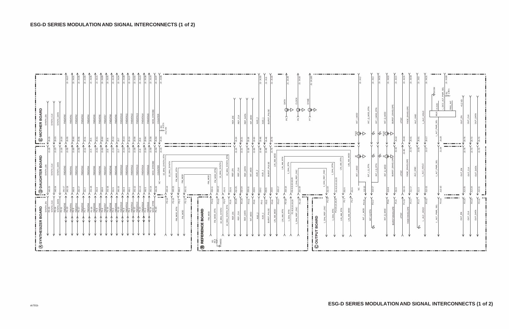
ESG-D SERIES MODULATION AND SIGNAL INTERCONNECTS (1 of 2)
OU
TP
UT
BO
AR
DC
INT
_I
_M
OD
P3
-15
+P
TA
T
BU
RS
T E
NV
EL
OP
E
INT
_Q
_M
OD
FA
DE
EN
VE
LO
PE
L _
AL
C _
HO
LD
P1
-6
P1
-15
P3
-6
P1
-3
P1
-17
P2
-22
L _
ALT
_ P
WR
_ S
EL
P2
-10
P2
-25
P2
-24
P2
-11
A
INT
I-Q
RT
N
P3
-17
AA A
A A
J1
- J4
,3
J1
- J4
,52
J1
- J4
,53
J1-
J4,5
7
J1-
J4,5
9
J5-4
2
J5-4
0
BU
RS
T_
EN
VE
LO
PE
+P
TA
T
INT
_Q
_M
OD
_R
TN
INT
_Q
_M
OD
INT
_I_
MO
D_
RT
N
INT
_I_
Q_
RT
N
INT
_I_
Q_
RT
N
J13
-17
INT
_Q
_M
OD
J13
-6
BU
RS
T_
EN
VE
LO
PE
+P
TA
T
J1-4
2
J1-4
0
J11
-6
J11
-15
J31
-19 1
_G
Hz_
RE
F_
OS
C1
_G
Hz_
RE
F_
OS
C
1_
GH
z_R
TN
1_
GH
z_R
TN
LIN
_A
M_
RT
NL
IN_
AM
_R
TN
LIN
_A
M_
MO
DL
IN_
AM
_M
OD
J31
-5
J11
-8,9
,10
,18
,20
J31
-6
J11
-191
_G
Hz_
RE
F_
OS
C
NC
P1
-2
P1
-19
P1
-8,9
,10
,18
,20
P1
-1
J1-
J4,5
8
J1
- J4
,8
J1
- J4
,31
J1
- J4
,80
J5-4
1
J5-9
1
J5-1
7
L_
ALT
_P
WR
_S
EL
J5-2
9
FA
DE
_E
NV
EL
OP
E
AL
C_
GN
D
L_
AL
C_
HO
LD
+5
.2V
D
TR
IG_
INT
L_
DC
C_
ALT
_P
WR
_S
EL
DC
OM
R1
1.9
6 k
MU
X
FA
DE
_E
NV
EL
OP
E
J1-4
1J1
1-1
7
AL
C_
GN
D
J1-9
1J1
1-3
L_
AL
C_
HO
LD
J1-1
7J1
2-2
2
L_
ALT
_P
WR
_S
EL
J1-2
9J1
2-1
0
+5
.2 V
D
J5-7
6
J5-7
3
J5-7
0
OU
T_
EN
OU
T_
CL
K
OU
T_
DA
TA
J1-7
6J1
2-2
5
J1-7
3J1
2-2
4
OU
T_
EN
OU
T_
CL
K
OU
T_
DA
TA
OU
T_
EN
OU
T_
CL
K
OU
T_
DA
TA
J1-7
0J1
2-1
1
J13
-15
INT
_I_
MO
D
J1
- J4
,2
INT
_I_
MO
DP
10
2J8
P1
03
J9
J31
-6
J33
-18
J31
-8,9
,10
,18
,20
J33
-17
1_
GH
z_R
TN
LIN
_A
M_
RT
N
LIN
_A
M_
MO
D
J5-4
6
J5-4
8
J5-7
9
AU
D_
2
AU
D_
1
BU
RS
T_
PU
LS
E
J1-
J4,5
5
J1
- J4
,6
J1
- J4
,30
P5
P6
P7
DA
TA
CL
OC
K
SY
MB
J1
- J4
,49
J1
- J4
,50
J1
- J4
,10
0
AU
D_
2
J1
-46
J3
3-2
AU
D_
1
J1
-48
J3
3-5
BU
RS
T_
PU
LS
E
J1
-79
J3
3-8
J5
-24
J5
-21
J5
-18
J5
-50
RE
F_
EN
RE
F_
CL
K
RE
F_
DA
TA
INT
_M
OD
J1
-24
J3
2-2
5
J1
-21
J3
2-2
4
J1
-18
J3
3-1
1
RE
F_
EN
RE
F_
CL
K
RE
F_
DA
TA
INT
_M
OD
J1
-50
J3
3-6
AU
D_
1
BU
RS
T_
PU
LS
E
AU
D_
2
P3
-5
P3
-2
P3
-8
P3
-17
P3
-18
P1
-8,9
,10
,18
,20
P1
-19
P1
-6
P2
-25
P2
-24
P3
-11
P3
-6
1_
GH
z_
RE
F_
OS
C
1_
GH
z_
RT
N
LIN
_A
M_
RT
N
LIN
_A
M_
MO
D
RE
F_
EN
RE
F_
CL
K
RE
F_
DA
TA
INT
_M
OD
DA
UG
HT
ER
BO
AR
DM
OT
HE
R B
OA
RD
DE
SY
NT
HE
SIZ
ER
BO
AR
DA
J1-1
1J5
-11
J41
-7
J1-5
J5-5
J41
-18
J1-1
3J5
-13
J41
-4
J1-1
4J5
-14
J41
-1
J1-5
9J5
-59
J41
-12
J1-8
J5-8
J41
-13
J1-6
4J5
-64
J41
-3
J1-5
8J5
-58
J41
-14
J41
-20
J1-5
4J5
-54
J1-1
5J5
-15
J1-6
1J5
-61
J41
-8
J1-6
2J5
-62
J41
-6
J1-6
J5-6
J41
-16
J1-1
2J5
-12
J41
-5
J1-7
J5-7
J41
-15
FM
DA
TA
5
FM
DA
TA
3
FM
DA
TA
4
FM
DA
TA
6
FM
DA
TA
7
FM
DA
TA
8
FM
DA
TA
11
FM
DA
TA
9
FM
DA
TA
10
FM
DA
TA
12
FM
DA
TA
13
FM
DA
TA
14
FM
DA
TA
15
CO
UN
TE
R
MO
D_
ST
RO
BE
FM
_M
OD
FM
_M
OD
_R
TN
P1
-11
P3
-15
P1
-2
P3
-14
FM
DA
TA
5
FM
DA
TA
3
FM
DA
TA
4
FM
DA
TA
6
FM
DA
TA
7
FM
DA
TA
8
FM
DA
TA
11
FM
DA
TA
9
FM
DA
TA
10
FM
DA
TA
12
FM
DA
TA
13
FM
DA
TA
14
FM
DA
TA
15
MO
D_
ST
RB
P1
-8
P1
-7
P1
-18
P1
-6
P1
-16
P1
-5
P1
-1
P1
-15
P1
-4
P1
-12
P1
-13
P1
-3
P1
-14
P1
-20
J1
- J4
,47
J1
- J4
,91
J1
- J4
,95
J1
- J4
,90
J1
- J4
,96
J1-
J4,8
8
J1
- J4
,37
J1
- J4
,92
J1-
J4,4
3
J1
- J4
,38
J1-
J4,4
4
J1-
J4,9
7
J1-
J4,8
6
J1-
J4,4
1
J1
- J4
,89
J1
- J4
,45
J1-
J4,3
9
J1
- J4
,94
FM
DA
TA
0
FM
DA
TA
1
FM
DA
TA
2
FM
DA
TA
5
FM
DA
TA
3
FM
DA
TA
4
FM
DA
TA
6
FM
DA
TA
7
FM
DA
TA
8
FM
DA
TA
11
FM
DA
TA
9
FM
DA
TA
10
FM
DA
TA
12
FM
DA
TA
13
FM
DA
TA
14
FM
DA
TA
15
CO
UN
TE
R
MO
D_
ST
RO
BE
NC
R3
4.2
2 k
+5
.2 V
D
J1-5
5J5
-55
J41
-19
J1-6
0J5
-60
J41
-9
J1-5
6J5
-56
J41
-17
FM
DA
TA
0
FM
DA
TA
1
FM
DA
TA
2
FM
DA
TA
0
FM
DA
TA
1
FM
DA
TA
2
P1
-19
P1
-9
P1
-17
J1-2
6J5
-26
J42
-25
J1-2
3J5
-23
J42
-24
J1-2
0J5
-20
J41
-17
SY
NT
H_
EN
SY
NT
H_
EN
SY
NT
H_
EN
SY
NT
H_
CL
KS
YN
TH
_C
LK
SY
NT
H_
CL
K
SY
NT
H_
DA
TA
SY
NT
H_
DA
TA
SY
NT
H_
DA
TA
P2
-25
P2
-24
P2
-11
J43
-15
J41
-2
J43
-14
J41
-11
FM
_M
OD
FM
_M
OD
_R
TN
10
_M
Hz_
SY
NT
H
10
_M
Hz_
SY
NT
H_
RT
N
FM
_M
OD
FM
_M
OD
_R
TN
J31
-5
J33
-12
J33
-11
10
_M
Hz_
SY
NT
H
10
_M
Hz_
SY
NT
H_
RT
N
RE
FE
RE
NC
E B
OA
RD
RE
FE
RE
NC
E B
OA
RD
BB
FM
_M
OD
_R
TN
FM
_M
OD
P3
-12
P1
-5
P3
-11
10
_M
Hz_
SY
NT
H
10
_M
Hz_
SY
NT
H_
RT
N
AM
OD
R2
46
.4
ESG-D SERIES MODULATION AND SIGNAL INTERCONNECTS (1 of 2)sk791b

ESG-D SERIES MODULATION AND SIGNAL INTERCONNECTS (2 of 2)
DATAGENERATORBOARD
HBASEBANDGENERATORBOARD
GDATAGENERATORBOARD
H
BURST_PULSE
P301-30
NC
NC
J1- J4,55
J1- J4,6
J1- J4,30
BURST_PULSE
P301-30
NC
NC
J1- J4,55
J1- J4,6
J1- J4,30
BASEBANDGENERATORBOARD
G
OPTIONS UN8 AND UN9OPTIONS UN3 AND UN4
EXT_DATA
P1-49
CLOCK
P1-50
SYNC
P1-100
J1- J4,49
J1- J4,50
J1- J4,100
BURST_GATE
P3-6
ADJ_TS_PWR_IN
BB_DATA
SYMBOL_SYNC
EXT_CLK
BBG_BIT_CLK
BBG_INT_CLK
BBG_EN
SUB_I_COUNT
P3-8
P3-10
P3-12
P3-14
P3-16
P3-18
P3-20
P3-22
NC
NC
EVENT 1
EVENT 2
BURSTGATE IN
PATTERNTRIG IN
EXT_BURST
PATTERN_TRIG
ALT_PWR_IN
EVENT (1) OUT
USER_DATA_EN
P2-2
P2-4
P2-6
P2-8
P2-10
P2-1,3,5,79,11,13,15
10K 100pf
P301-3
P301-52
J1- J4,3
J1- J4,52
J1- J4,53
J1- J4,57
J1- J4,59
INT_Q_MOD_RTN
INT_Q_MOD
INT_I_MOD_RTN
P301-53
BURST_ENVELOPE
P301-57
ACOM
ACOM
NC
NC
NC
INTL_ALC_HOLD
P301-31
L_ALT_PWR_SEL
P301-80
J1- J4,58
J1- J4,8
J1- J4,31
J1- J4,80
INT_I_MOD
P301-2J1- J4,2
BURST_GATE
P300-6
ADJ_TS_PWR_IN
BB_DATA
SYMBOL _SYNC
P300-8
P300-10
P300-12
BBG_INT_CLK
BBG_EN
SUB_I_COUNT
P300-18
P300-20
P300-22
EXT_CLK
BBG_BIT_CLK
P300-14
P300-16
RE
AR
PA
NE
L
Q_OUTQ-OUT
I_OUTI-OUT
P404
P405(RP)
(RP)
BURST_GATE
P3-6
ADJ_TS_PWR_IN
BB_DATA
SYMBOL_SYNC
EXT_CLK
BBG_BIT_CLK
BBG_INT_CLK
BBG_EN
SUB_I_COUNT
P3-8
P3-10
P3-12
P3-14
P3-16
P3-18
P3-20
P3-22
NC
NC
NC
EVENT 1
EVENT 2
BURSTGATE IN
PATTERNTRIG IN
EXT_BURST
PATTERN_TRIG
ALT_PWR_IN
EVENT (1) OUT
USER_DATA_EN
P2-2
P2-4
P2-6
P2-8
P2-10
P2-1,3,5,79,11,13,15
10K 100pf
P301-3
P301-52
J1- J4,3
J1- J4,52
J1- J4,53
J1- J4,57
J1- J4,59
INT_Q_MOD_RTN
INT_Q_MOD
INT_I_MOD_RTN
P301-53
BURST_ENVELOPE
P301-57
ACOM
ACOM
NC
NC
NC
INTL_ALC_HOLD
P301-31
L_ALT_PWR_SEL
P301-80
J1- J4,58
J1- J4,8
J1- J4,31
J1- J4,80
INT_I_MOD
P301-2J1- J4,2
BURST_GATE
P300-6
ADJ_TS_PWR_IN
BB_DATA
SYMBOL _SYNC
P300-8
P300-10
P300-12
BBG_INT_CLK
BBG_EN
SUB_I_COUNT
P300-18
P300-20
P300-22
EXT_CLK
BBG_BIT_CLK
P300-14
P300-16
RE
AR
PA
NE
L
Q_OUTQ-OUT
I_OUTI-OUT
P404
P405(RP)
(RP)
OPTION 300
DEMODULATORJ
SPR FUZZY
DOWN CONV
V1-1 P16-1
IF IN
DOWN CONV
V1-3 P7-1
FREQ_REF
(RP)(RP)
BER SYNC LOSS
P5-2
SYNC_LOSS_IN
(RP)
BER NO DATA
P15-4
NO_DATA_IN
(RP)
BER MEAS END
P5-6
MES_END_IN
(RP)
BER ERROR OUT
P5-8
ERR_IN
(RP)
BER TEST OUT TEST_IN
BERT BOARD
P2-1 P9-1
DATA
BERT BOARD
P1-1
CLOCK
P10-1
BERT BOARD
P3-1 P8-1
GATE
BER CLK IN
(RP) P13-1
EXT_CLOCK
(RP)
BER DATA IN
P12-1
EXT_DATA
(RP)
BER GATE IN
P11-1
EXT_GATE
SPR_FUZZY_INO
P3-4
SPR_FUZZY_INO
P3-16
SPR_FUZZY_INO
P3-22
P2-4
PATTERN TRIG IN PATTERN_TRIG_IN
(RP)
EVENT 1 EVENT_1
(RP) P2-8
EVENT 2 EVENT_2
(RP) P2-10
DATA OUT DATA_IN
(RP) P2-12
DATA CLK OUT DATA_CLK_IN
(RP) P2-14
SYMBOL SYNC OUT SYMBOL_SYNC_IN
(RP) P2-16
J1-J4, 49
EXT_DATA_IN
P1-49
J1-J4, 50
EXT_CLK_IN
P1-50
J1-J4, 85
BBG_TRIG_INT
P1-85
J1-J4, 100
EXT_SYNC_IN
P1-100
P2-1, 3, 5, 7, 9, 11, 13, 15
DIGITAL CARD CAGE F
J1- J4,37,38,39,41,43,44,45,47,86,88,89,90,91,92,94,95,96,97
NC
BURST_PULSE
AUD1
AUD2
P2-30
P2-6
P2-55J1- J4,55
J1- J4,6
J1- J4,30
DUAL ARBITRARYWAVEFORMGENERATORBOARD(OPTION UND)
I
Q_OUTQ-OUT
I_OUTI-OUT
J2
J1(RP)
(RP)
P2-52J1- J4,52
INT_I_MOD_RTN
EVENT1_OUT
EVENT2_OUT
(RP)
(RP)
EVENT 1
EVENT 2
P1-8
P1-10
ACOM
J1- J4,53
INT_Q_MOD
P2-53
J1- J4,4
ABUS
P2-4
J1- J4,5
ABUS_RTN
P2-5
NC
NC
J1- J4,58
J1- J4,8
INTL_ALC_HOLD
P2-31J1- J4,31
L_ALT_PWR_SEL
P2-80J1- J4,80
P2-3J1- J4,3
INT_Q_MOD_RTN
ACOM
INT_I_MOD
P2-2J1- J4,2
EXT_DATA
P2-49J1- J4,49
CLOCK
P2-50J1- J4,50
SYNC
P2-100J1- J4,100
ESG-D SERIES MODULATION AND SIGNAL INTERCONNECTS (2 of 2)sk792b

ESG Family Signal Generators
3 Replaceable Parts(ESG-A and ESG-D Series)
This chapter provides important ordering information and lists the part numbers for the various replaceable parts, kits, and accessories available for your signal generator. This chapter is also useful for locating and identifying assemblies and cables.
Service Guide 3-1

Replaceable Parts (ESG-A and ESG-D Series) ESG Family Signal GeneratorsOrdering Information
Ordering InformationTo order a part listed in the replaceable parts lists, do the following:
1. Determine the part number.
2. Determine the quantity required.
3. Mail this information to the nearest Agilent Technologies office or, in the U.S., call the hotline number listed in the following section.
To order a part not listed in the replaceable parts lists, mail the following information to the nearest Agilent Technologies office or, in the U.S., call the hotline number listed in the following section.
1. the instrument model number
2. the serial number and options, if any (see rear panel)
3. a description of the part
4. a description of the part’s function
5. the quantity required
Call (800) 227-8164 to Order Parts Fast (U.S. Only)When you have gathered the information required to place an order, contact Agilent Technologies’ direct ordering team by calling the toll-free hotline number shown above. Orders may be placed Monday through Friday, 6 AM to 5 PM (Pacific Standard Time).
The parts specialists have direct on-line access to replacement parts inventory corresponding to the replaceable parts lists in this manual. Four day delivery time is standard; there is a charge for hotline one-day delivery.
This information applies to the United States only. Outside the United States, you must contact the nearest Agilent Technologies sales and service office. (Refer to Table 1-1 on page 1-9.)
3-2 Service Guide

ESG Family Signal Generators Replaceable Parts (ESG-A and ESG-D Series)Save Money with Rebuilt-Exchange Assemblies
Save Money with Rebuilt-Exchange AssembliesUnder the rebuilt-exchange assembly program, certain factory-repaired and tested assemblies are available on a trade-in basis. These assemblies cost less than a new assembly, and meet all factory specifications required of a new assembly.
The defective assembly must be returned for credit under the terms of the rebuilt-exchange assembly program. The figure below illustrates the assembly exchange procedure in flowchart format.
Assembly Exchange Procedure
Service Guide 3-3

Replaceable Parts (ESG-A and ESG-D Series) ESG Family Signal GeneratorsSave Money with Rebuilt-Exchange Assemblies
Shipping the Defective Assembly Back to Agilent Technologies
1. When you receive the rebuilt assembly, be careful not to damage the box in which it was shipped. You will use that box to return the defective assembly. The box you receive should contain the following:
• the rebuilt assembly
• an exchange assembly failure report
• a return address label
2. Complete the failure report.
3. Place the failure report and the defective assembly in the box. Be sure to remove the enclosed return address label.
4. Seal the box with tape.
If you are inside the United States, stick the preprinted return address label over the label that is already on the box and return the box to Agilent Technologies. (Agilent Technologies pays postage on boxes mailed within the United States.)
If you are outside the USA, do not use the return address label; instead, address the box to the nearest Agilent Technologies sales and service office. (Refer to Table 1-1 on page 1-9.)
3-4 Service Guide

ESG Family Signal Generators Replaceable Parts (ESG-A and ESG-D Series)Abbreviations Used in Part Descriptions
Abbreviations Used in Part DescriptionsThis section defines the reference designators, abbreviations, and option numbers that are used in the part descriptions throughout this chapter.
Reference Designations
Abbreviations
Reference Designator
Definition
A assembly
AT attenuator
B fan
DS lamp
J electrical connector; jack
P electrical connector; plug
W cable; transmission path; wire
Abbreviation Definition
Assy assembly
Bd board
BC beryllium
BN buttonhead (screws)
CPU central processing unit
CW conical washer (screws)
CY copper
D diameter
ESD electrostatic discharge
EXT external
FL flathead (screws)
Ft feet
Hex hexagonal
GPIB general purpose interface bus
HX hexagonal recess (screws)
I in-phase
ID inside diameter
L length
Service Guide 3-5
Replaceable Parts (ESG-A and ESG-D Series) ESG Family Signal GeneratorsAbbreviations Used in Part Descriptions
Hardware Options
LF low frequency
M meters or metric hardware
OD outside diameter
PC patch lock (screws) or printed circuit
PN panhead (screws)
Q quadrature
Qty quantity
REF reference
RF radio frequency
RFI radio frequency interference
RPP reverse power protection
SH socket head cap (screws)
SMA subminiature type-A
SMB subminiature type-B
TX TORX recess (screws)
V volt
Options Definition
300 Base Station BERT Extension for Option UN7
1E5 Precision Frequency Reference
1E6 High Performance Pulse Input
1EM Rear Panel Connections
UN3 Baseband Generator - 1 Meg
UN4 Baseband Generator - 8 Meg
UN7 Bit Error Rate Test
UN8 Real-Time I/Q Baseband Generator - 1 Meg
UN9 Adds 7 Meg RAM to UN8
UNA Alternate Timeslot Power
UNB High Power with Mechanical Attenuator
UND Dual Arbitrary Waveform Generator
Abbreviation Definition
3-6 Service Guide

ESG Family Signal Generators Replaceable Parts (ESG-A and ESG-D Series)Major Assemblies
Major AssembliesThis section lists part numbers for the major assemblies in your signal generator. The following instrument views are provided to help you locate specific assemblies.
• “Top View” on page 3-8
• “Top View (ESG-D Series - Option 300)” on page 3-10
• “Right Side Assemblies” on page 3-12
• “Disassembled Front Panel View” on page 3-13
• “Inside Rear Panel View” on page 3-14
Service Guide 3-7

Replaceable Parts (ESG-A and ESG-D Series) ESG Family Signal GeneratorsMajor Assemblies
Top ViewRefer to Table 3-1 and Figure 3-1.
Table 3-1 Top View
Reference Designator
Part Number Qty Description
A4 0950-2791 1 Assy-Power Supply
A5 E4400-60187 1 Bd Assy-Dual Arbitrary Waveform Generator (Option UND)
A5 E4400-69187 Exchange Bd Assy-Dual Arbitrary Waveform Generator (Option UND)
A6 E4400-60072 1 Bd Assy-Bit Error Rate Test (Option UN7)
A6 E4400-69072 Exchange Bd Assy-Bit Error Rate Test (Option UN7)
A7 E4400-60048 1 Bd Assy-Baseband Generator (Options UN3, UN4)
A7 E4400-69048 Exchange Bd Assy-Baseband Generator (Options UN3, UN4)
A7 E4400-60070 1 Bd Assy-Real-Time I/Q Baseband Generator (Options UN8, UN8+UN9)
A7 E4400-69070 Exchange Bd Assy-Real-Time I/Q Baseband Generator(Options UN8, UN8+UN9)
A8 E4400-60043 1 Bd Assy-Data Generator, 1 Meg (Option UN3)
A8 E4400-69043 Exchange Bd Assy-Data Generator, 1 Meg (Option UN3)
A8 E4400-60057 1 Bd Assy-Data Generator, 8 Meg (Option UN4)
A8 E4400-69057 Exchange Bd Assy-Data Generator, 8 Meg (Option UN4)
A8 E4400-60182 1 Bd Assy-Data Generator, 1 Meg (Option UN8)
A8 E4400-69182 Exchange Bd Assy-Data Generator, 1 Meg (Option UN8)
A8 E4400-60183 1 Bd Assy-Data Generator, 8 Meg (Option UN8+UN9)
A8 E4400-69183 Exchange Bd Assy-Data Generator, 8 Meg (Option UN8+UN9)
A8 E4400-60154 1 Bd Assy-Flex Data Generator, 1 Meg (Option UN8)
A8 E4400-69154 Exchange Bd Assy-Flex Data Generator, 1 Meg (Option UN8)
A8 E4400-60195 1 Bd Assy-Flex Data Generator, 8 Meg (Option UN8+UN9)
A8 E4400-69195 Exchange Bd Assy-Flex Data Generator, 8 Meg (Option UN8+UN9)
A14 E4400-60220 1 Replacement Kit-CPU/Motherboard (serial no. prefixes < US3934/GB3934)
A14 E4400-60225 1 Replacement Kit-CPU/Motherboard (serial no. prefixes ≥ US3934/GB3934)
A14BT1 1420-0338 1 Battery-Lithium
AT1 E4400-60042 1 Assy-Electronic Attenuator/RPP (Option UNA) replaced by E4400-60681
AT1 E4400-60680 1 Assy-Electronic Attenuator/RPP
AT1 E4400-60681 1 Assy-Electronic Attenuator/RPP upgrade kit (for E4400-60042 and E4400-60205)
AT1 33322-60014 1 Assy-Mechanical Attenuator (Option UNB)
A19 08648-60025 1 Assy-RPP (Option UNB)
3-8 Service Guide

ESG Family Signal Generators Replaceable Parts (ESG-A and ESG-D Series)Major Assemblies
Figure 3-1 Top View
A25 08648-60010 1 Pulse Modulator Assembly (Option 1E6)
B1 E4400-60218 1 Assy-Fan, Small
B2 E4400-60062 1 Kit-Fan, Large (includes 2 foam strips)
Reference Designator
Part Number Qty Description
Service Guide 3-9

Replaceable Parts (ESG-A and ESG-D Series) ESG Family Signal GeneratorsMajor Assemblies
Top View (ESG-D Series - Option 300)Refer to Table 3-2 and Figure 3-2.
Table 3-2 Top View (ESG-D Series - Option 300)
Reference Designator
Part Number Qty Description
A4 0950-2791 1 Assy-Power Supply
A6 E4400-60507 1 Bd Assy-Bit Error Rate Test (Option UN7)
A6 E4400-69072 Exchange Bd Assy-Bit Error Rate Test (Option UN7)
A7 E4400-60070 1 Bd Assy-Real-Time I/Q Baseband Generator (Options UN8 or UN8+UN9)
A7 E4400-69070 Exchange Bd Assy-Real-Time I/Q Baseband Generator(Options UN8 or UN8+UN9)
A8 E4400-60154 1 Bd Assy-Flex Data Generator, 1 Meg (Option UN8)
A8 E4400-69154 Exchange Bd Assy-Flex Data Generator, 1 Meg (Option UN8)
A8 E4400-60195 1 Bd Assy-Flex Data Generator, 8 Meg (Option UN8+UN9)
A8 E4400-69195 Exchange Bd Assy-Flex Data Generator, 8 Meg (Option UN8+UN9)
A14 E4400-60220 1 Replacement Kit-CPU/Motherboard (serial no. prefixes < US3934/GB3934)
A14 E4400-60225 1 Replacement Kit-CPU/Motherboard (serial no. prefixes ≥ US3934/GB3934)
A14BT1 1420-0338 1 Battery-Lithium
AT1 E4400-60042 1 Assy-Electronic Attenuator/RPP (Option UNA) replaced by E4400-60681
AT1 E4400-60680 1 Assy-Electronic Attenuator/RPP
AT1 E4400-60681 1 Assy-Electronic Attenuator/RPP upgrade kit (for E4400-60042 and E4400-6205)
A20 E4400-60200 1 Bd Assy-Downconvertor
A20 E4400-69200 1 Exchange Bd Assy-Downconvertor
A21 E4400-60241 1 Bd Assy-Demodulator
A21 E4400-69199 Exchange Assy-Demodulator
B1 E4400-60218 1 Assy-Fan, Small
B2 E4400-60062 1 Kit-Fan, Large (includes 2 foam strips)
3-10 Service Guide

ESG Family Signal Generators Replaceable Parts (ESG-A and ESG-D Series)Major Assemblies
Figure 3-2 Top View (ESG-D Series - Option 300)
Service Guide 3-11

Replaceable Parts (ESG-A and ESG-D Series) ESG Family Signal GeneratorsMajor Assemblies
Right Side AssembliesRefer to Table 3-3 and Figure 3-3.
Table 3-3 Replaceable Assemblies, Right Side
Figure 3-3 Right Side View
Reference Designator
Part Number Qty Description
A9 E4400-60038 1 Bd Assy-Output (ESG-A series with serial no. prefixes≤ US3926/GB3926 or ≥ US3934/GB3934)
A9 E4400-69038 1 Exchange Bd Assy-Output (ESG-A series with serial no. prefixes≤ US3926/GB3926 or ≥ US3934/GB3934)
A9 E4400-60003 1 Bd Assy-Output (ESG-A series with serial no. prefix US3927/GB3927)
A9 E4400-69003 1 Exchange Bd Assy-Output (ESG-A series with serial no. prefix US3927/GB3927)
A9 E4400-60003 1 Bd Assy-Output (ESG-D Series)
A9 E4400-69003 1 Exchange Bd Assy-Output (ESG-D Series)
A9 E4400-60141 1 Bd Assy-Output (All models with Option UNB)
A9 E4400-69141 1 Exchange Bd Assy-Output (All models with Option UNB)
A11 E4400-60243 1 Bd Assy-Reference, TCXO
A11 E4400-69243 1 Exchange Bd Assy-Reference, TCXO
A11 E4400-60242 1 Bd Assy-Reference, OCXO (Option 1E5)
A11 E4400-69242 1 Exchange Bd Assy-Reference, OCXO (Option 1E5)
A12 E4400-60180 1 Bd Assy-Synthesizer/Doubler
A12 E4400-69180 1 Exchange Bd Assy-Synthesizer/Doubler
A15 E4400-60138 1 Bd Assy-Daughter
3-12 Service Guide

ESG Family Signal Generators Replaceable Parts (ESG-A and ESG-D Series)Major Assemblies
Disassembled Front Panel ViewRefer to Table 3-4 and Figure 3-4.
Table 3-4 Disassembled Front Panel View
Figure 3-4 Disassembled Front Panel View
Reference Designator
Part Number Qty Description
A1 E4400-60211 1 Bd Assy-Front Panel
A2 1990-1910 1 Assy-Display, Wide-Angle View (serial no. prefixes < US3934/GB3934)
A2 2090-0375 1 Assy-Display, Wide-Angle View (serial no. prefixes ≥ US3934/GB3934)
A2DS1 1513-5204 1 Lamp-Fluorescent
A3 0950-3093 1 Assy-Inverter
Service Guide 3-13
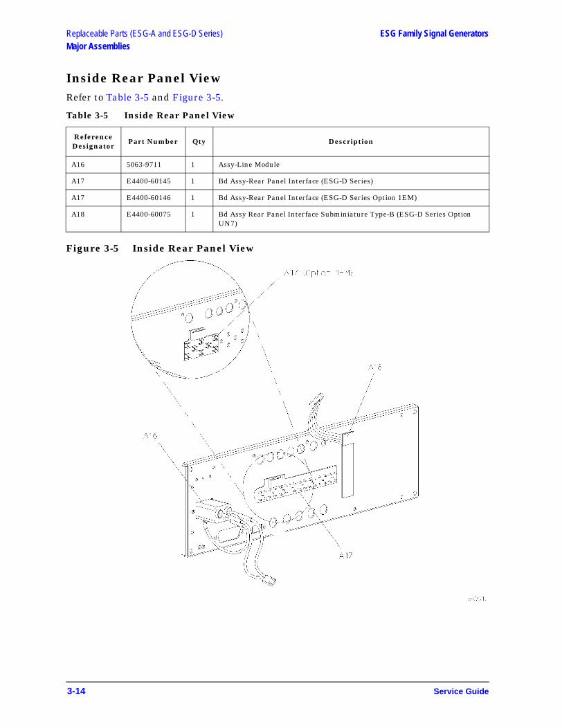
Replaceable Parts (ESG-A and ESG-D Series) ESG Family Signal GeneratorsMajor Assemblies
Inside Rear Panel ViewRefer to Table 3-5 and Figure 3-5.
Table 3-5 Inside Rear Panel View
Figure 3-5 Inside Rear Panel View
Reference Designator
Part Number Qty Description
A16 5063-9711 1 Assy-Line Module
A17 E4400-60145 1 Bd Assy-Rear Panel Interface (ESG-D Series)
A17 E4400-60146 1 Bd Assy-Rear Panel Interface (ESG-D Series Option 1EM)
A18 E4400-60075 1 Bd Assy Rear Panel Interface Subminiature Type-B (ESG-D Series Option UN7)
3-14 Service Guide

ESG Family Signal Generators Replaceable Parts (ESG-A and ESG-D Series)Cables
CablesThis section lists part numbers for the cables in your signal generator. The following instrument views are provided to help you locate specific cables.
• “Top View (ESG-A Series)” on page 3-16
• “Top View (ESG-D Series - Options UN3/4, UN7)” on page 3-18
• “Top View (ESG-D Series - Options UN7, UN8)” on page 3-20
• “Top View (ESG-D Series - Option UND)” on page 3-22
• “Top View (ESG-D Series - Options UN3/4, UN7 with 1EM)” on page 3-24
• “Top View (ESG-D Series - Options UN7, UN8 with 1EM)” on page 3-26
• “Top View (ESG-D Series - Options UN7, UN8, UND)” on page 3-28
• “Top View (ESG-D Series - Option UND with 1EM)” on page 3-30
• “Top View (ESG-D Series - Option 300)” on page 3-32
• “Inside Front Panel View” on page 3-34
• “Electronic Attenuator/RPP View” on page 3-36
• “Electronic Attenuator/RPP View (with Option 1EM)” on page 3-38
• “Mechanical Attenuator View (Option UNB)” on page 3-40
• “Mechanical Attenuator View (Option UNB with 1EM)” on page 3-42
• “Pulse Modulator View (Option 1E6)” on page 3-44
Service Guide 3-15

Replaceable Parts (ESG-A and ESG-D Series) ESG Family Signal GeneratorsCables
Top View (ESG-A Series)Refer to Table 3-6 and Figure 3-6.
Table 3-6 Top View (ESG-A Series)
Reference Designator
Part Number Qty Description
A4W1*
*. This cable is not replaceable by itself. You must order the corresponding assembly.
(part of A4) 1 Power Supply (A4) to CPU/Motherboard (A14J6)
A16W1* (part of A16) 1 Line Module (A16) to Power Supply (A4J1)
A16W2* (part of A16) 1 Line Module (A16) to Chassis Ground Post on Rear Panel
3-16 Service Guide
ESG Family Signal Generators Replaceable Parts (ESG-A and ESG-D Series)Cables
Figure 3-6 Top View (ESG-A Series)
Service Guide 3-17

Replaceable Parts (ESG-A and ESG-D Series) ESG Family Signal GeneratorsCables
Top View (ESG-D Series - Options UN3/4, UN7)Refer to Table 3-7 and Figure 3-7.
Table 3-7 Top View (ESG-D Series - Options UN3/4, UN7)
Reference Designator
Part Number Qty Description
A4W1*
*. This cable is not replaceable by itself. You must order the corresponding assembly.
(part of A4) 1 Power Supply (A4) to CPU/Motherboard (A14J6)
A16W1* (part of A16) 1 Line Module (A16) to Power Supply (A4J1)
A16W2* (part of A16) 1 Line Module (A16) to Chassis Ground Post on Rear Panel
A18W1* (part of A18) 1 BERT Rear Panel Interface Board (A18) to BERT (A6)
W3 8120-5063 1 DATA to Data Generator (A8J2)
W4 8120-5063 1 DATA CLOCK to Data Generator (A8J1)
W5 8120-5063 1 SYMBOL SYNC to Data Generator (A8J3)
W15 8120-5055 1 Baseband Generator (A7P403) to BASEBAND GENREF IN
W16 8120-5055 1 Baseband Generator (A7P404) to Rear Panel (Q OUT)
W17 8120-5055 1 Baseband Generator (A7P405) to Rear Panel (I OUT)
W18 8120-8458 1 Rear Panel Interface Board (A17) to Data Generator (A8P2) (Options UN3/4)
W19 8120-8349 1 Baseband Generator (A7P300) to Data Generator (A8P3) (Options UN3/4)
W21 8120-5055 1 Bit Error Rate Test Board (A6) to BER GATE IN (Options UN3/4 and UN7)
W22 8120-5055 1 Bit Error Rate Test Board (A6) to BER CLK IN (Options UN3/4 and UN7)
W23 8120-5055 1 Bit Error Rate Test Board (A6) to BER DATA IN (Options UN3/4 and UN7)
3-18 Service Guide

ESG Family Signal Generators Replaceable Parts (ESG-A and ESG-D Series)Cables
Figure 3-7 Top View (ESG-D Series - Options UN3/4, UN7)
Service Guide 3-19

Replaceable Parts (ESG-A and ESG-D Series) ESG Family Signal GeneratorsCables
Top View (ESG-D Series - Options UN7, UN8)Refer to Table 3-8 and Figure 3-8.
Table 3-8 Top View (ESG-D Series - Options UN7, UN8)
Reference Designator
Part Number Qty Description
A4W1*
*. This cable is not replaceable by itself. You must order the corresponding assembly.
(part of A4) 1 Power Supply (A4) to CPU/Motherboard (A14J6)
A16W1* (part of A16) 1 Line Module (A16) to Power Supply (A4J1)
A16W2* (part of A16) 1 Line Module (A16) to Chassis Ground Post on Rear Panel
A18W1* (part of A18) 1 BERT Rear Panel Interface Board (A18) to BERT (A6)
W3 8120-5063 1 DATA to Motherboard (A14P5)
W4 8120-5063 1 DATA CLOCK to Motherboard (A14P6)
W5 8120-5063 1 SYMBOL SYNC to Motherboard (A14P7)
W15 8120-5055 1 Baseband Generator (A7P403) to BASEBAND GENREF IN
W16 8120-5055 1 Baseband Generator (A7P404) to Rear Panel (Q OUT)
W17 8120-5055 1 Baseband Generator (A7P405) to Rear Panel (I OUT)
W18 8120-8457 1 Rear Panel Interface Board (A17) to Data Generator (A8P2) and Baseband Generator (A7P2) (Option UN8 - connects in three places)
W19 8120-8349 1 Baseband Generator (A7P300) to Data Generator (A8P3) (Option UN8)
W21 8120-5055 1 Bit Error Rate Test Board (A6) to BER GATE IN (Options UN7, UN8)
W22 8120-5055 1 Bit Error Rate Test Board (A6) to BER CLK IN (Options UN7, UN8)
W23 8120-5055 1 Bit Error Rate Test Board (A6) to BER DATA IN (Options UN7, UN8)
W27 8120-8725 1 16-Pin Ribbon Cable, Parallel Data In, Data Generator (A8) to Baseband Generator (A7)
3-20 Service Guide
ESG Family Signal Generators Replaceable Parts (ESG-A and ESG-D Series)Cables
Figure 3-8 Top View (ESG-D Series - Options UN7, UN8)
Service Guide 3-21

Replaceable Parts (ESG-A and ESG-D Series) ESG Family Signal GeneratorsCables
Top View (ESG-D Series - Option UND)Refer to Table 3-9 and Figure 3-9.
Table 3-9 Top View (ESG-D Series - Option UND)
Reference Designator
Part Number Qty Description
A4W1*
*. This cable is not replaceable by itself. You must order the corresponding assembly.
(part of A4) 1 Power Supply (A4) to CPU/Motherboard (A14J6)
A16W1* (part of A16) 1 Line Module (A16) to Power Supply (A4J1)
A16W2* (part of A16) 1 Line Module (A16) to Chassis Ground Post on Rear Panel
W15 8120-5055 1 Dual Arb Waveform Generator (A5) to BASEBAND GEN REF
W16 8120-5055 1 Dual Arb Waveform Generator (A5) to Q OUT
W17 8120-5055 1 Dual Arb Waveform Generator (A5) to I OUT
W18 8120-8458 1 Rear Panel Interface Board (A17) to Dual Arb Waveform Generator (A5)
W18 8120-8457 1 Rear Panel Interface Board (A17) to Data Generator (A8P2), Baseband Generator (A7P2), and Dual Arb Waveform Generator (A5) (Option UN8 - connects in three places)
W24 E4400-20131 1 Baseband Generator - 13 MHz (A7) to Dual Arb Waveform Generator - 13 MHz (A5) (Option UN3 or UN4)
3-22 Service Guide

ESG Family Signal Generators Replaceable Parts (ESG-A and ESG-D Series)Cables
Figure 3-9 Top View (ESG-D Series - Option UND)
Service Guide 3-23

Replaceable Parts (ESG-A and ESG-D Series) ESG Family Signal GeneratorsCables
Top View (ESG-D Series - Options UN3/4, UN7 with 1EM)Refer to Table 3-10 and Figure 3-10.
Table 3-10 Top View (ESG-D Series - Options UN3/4, UN7 with 1EM)
Reference Designator
Part Number Qty Description
A4W1*
*. This cable is not replaceable by itself. You must order the corresponding assembly.
(part of A4) 1 Power Supply (A4) to CPU/Motherboard (A14J6)
A16W1* (part of A16) 1 Line Module (A16) to Power Supply (A4J1)
A16W2* (part of A16) 1 Line Module (A16) to Chassis Ground Post on Rear Panel
A18W1* (part of A18) 1 BERT Rear Panel Interface Board (A18) to BERT (A6) (Option UN7)
W3 8120-5556 1 DATA to Data Generator (A8J2) (Options UN3/4)
W4 8120-5556 1 DATA CLOCK to Data Generator (A8J1) (Options UN3/4)
W5 8120-5556 1 SYMBOL SYNC to Data Generator (A8J3) (Options UN3/4)
W15 8120-5556 1 Baseband Generator (A7P403) to BASEBAND GENREF IN (Options UN3/4)
W16 8120-5556 1 Baseband Generator (A7P404) to Q OUT (Options UN3/4)
W17 8120-5556 1 Baseband Generator (A7P405) to I OUT (Options UN3/4)
W18 8120-8458 1 Rear Panel Interface Board (A17) to Data Generator (A8P2) (Options UN3/4)
W19 8120-8349 1 Baseband Generator (A7P300) to Data Generator (A8P3) (Options UN3/4)
W21 8120-5556 1 Bit Error Rate Test Board (A6) to BER GATE IN (Option UN7)
W22 8120-5556 1 Bit Error Rate Test Board (A6) to BER CLK IN (Option UN7)
W23 8120-5556 1 Bit Error Rate Test Board (A6) to BER DATA IN (Option UN7)
3-24 Service Guide

ESG Family Signal Generators Replaceable Parts (ESG-A and ESG-D Series)Cables
Figure 3-10 Top View (ESG-D Series - Options UN3/4, UN7 with 1EM)
Service Guide 3-25

Replaceable Parts (ESG-A and ESG-D Series) ESG Family Signal GeneratorsCables
Top View (ESG-D Series - Options UN7, UN8 with 1EM)Refer to Table 3-11 and Figure 3-11.
Table 3-11 Top View (ESG-D Series - Options UN7, UN8 with 1EM)
Reference Designator
Part Number Qty Description
A4W1*
*. This cable is not replaceable by itself. You must order the corresponding assembly.
(part of A4) 1 Power Supply (A4) to CPU/Motherboard (A14J6)
A16W1* (part of A16) 1 Line Module (A16) to Power Supply (A4J1)
A16W2* (part of A16) 1 Line Module (A16) to Chassis Ground Post on Rear Panel
A18W1* (part of A18) 1 BERT Rear Panel Interface Board (A18) to BERT (A6) (Option UN7)
W3 8120-5556 1 DATA to Data Generator (A8J2) (Option UN8)
W4 8120-5556 1 DATA CLOCK to Data Generator (A8J1) (Option UN8)
W5 8120-5556 1 SYMBOL SYNC to Data Generator (A8J3) (Option UN8)
W15 8120-5556 1 Baseband Generator (A7P403) to BASEBAND GENREF IN (Option UN8)
W16 8120-5556 1 Baseband Generator (A7P404) to Q OUT (Option UN8)
W17 8120-5556 1 Baseband Generator (A7P405) to I OUT (Option UN8)
W18 8120-8457 1 Rear Panel Interface Board (A17) to Data Generator (A8P2) and Baseband Generator (A7P2) (Option UN8 - connects in three places)
W19 8120-8349 1 Baseband Generator (A7P300) to Data Generator (A8P3) (Option UN8)
W21 8120-5556 1 Bit Error Rate Test Board (A6) to BER GATE IN (Option UN7)
W22 8120-5556 1 Bit Error Rate Test Board (A6) to BER CLK IN (Option UN7)
W23 8120-5556 1 Bit Error Rate Test Board (A6) to BER DATA IN (Option UN7)
W27 8120-8725 1 16-Pin Ribbon Cable, Parallel Data In, Data Generator (A8) to Baseband Generator (A7)
3-26 Service Guide
ESG Family Signal Generators Replaceable Parts (ESG-A and ESG-D Series)Cables
Figure 3-11 Top View (ESG-D Series - Options UN7, UN8 with 1EM)
Service Guide 3-27
Replaceable Parts (ESG-A and ESG-D Series) ESG Family Signal GeneratorsCables
Top View (ESG-D Series - Options UN7, UN8, UND)Refer to Table 3-12 and Figure 3-12.
Table 3-12 Top View (ESG-D Series - Options UN7, UN8, UND)
Reference Designator
Part Number Qty Description
A4W1*
*. This cable is not replaceable by itself. You must order the corresponding assembly.
(part of A4) 1 Power Supply (A4) to CPU/Motherboard (A14J6)
A16W1* (part of A16) 1 Line Module (A16) to Power Supply (A4J1)
A16W2* (part of A16) 1 Line Module (A16) to Chassis Ground Post on Rear Panel
A18W1* (part of A18) 1 BERT Rear Panel Interface Board (A18) to BERT (A6) (Option UN7)
W3 8120-5556 1 DATA to Data Generator (A8J2) (Option UN8)
W4 8120-5556 1 DATA CLOCK to Data Generator (A8J1) (Option UN8)
W5 8120-5556 1 SYMBOL SYNC to Data Generator (A8J3) (Option UN8)
W15 8120-5556 1 Baseband Generator (A7P403) to BASEBAND GENREF IN (Option UN8)
W16 8120-5556 1 Baseband Generator (A7P404) to Q OUT (Option UN8)
W17 8120-5556 1 Baseband Generator (A7P405) to I OUT (Option UN8)
W18 8120-8457 1 Rear Panel Interface Board (A17) to Data Generator (A8P2) and Baseband Generator (A7P2) (Option UN8 - connects in three places)
W19 8120-8349 1 Baseband Generator (A7P300) to Data Generator (A8P3) (Option UN8)
W21 8120-5556 1 Bit Error Rate Test Board (A6) to BER GATE IN (Option UN7)
W22 8120-5556 1 Bit Error Rate Test Board (A6) to BER CLK IN (Option UN7)
W23 8120-5556 1 Bit Error Rate Test Board (A6) to BER DATA IN (Option UN7)
W24 E4400-20131 1 Baseband Generator-13 MHz (A7) to Dual Arb Waveform Generator - 13 MHz (A5) (Option UN3 or UN4)
W25 8120-8748 1 Motherboard (A14P103) to Daughterboard - Q INT (A15J8)
W26 8120-8748 1 Motherboard (A14P102) to Daughterboard - I INT (A15J9)
W27 8120-8725 1 16-Pin Ribbon Cable, Parallel Data In, Data Generator (A8) to Baseband Generator (A7)
3-28 Service Guide
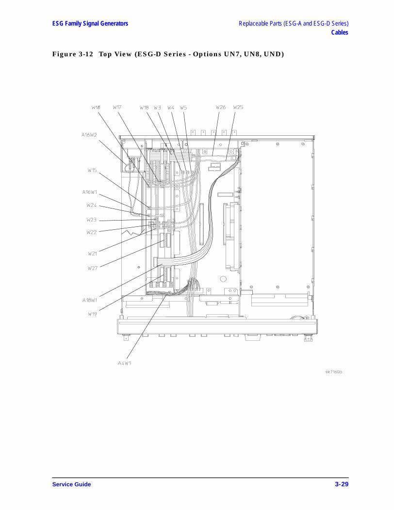
ESG Family Signal Generators Replaceable Parts (ESG-A and ESG-D Series)Cables
Figure 3-12 Top View (ESG-D Series - Options UN7, UN8, UND)
Service Guide 3-29
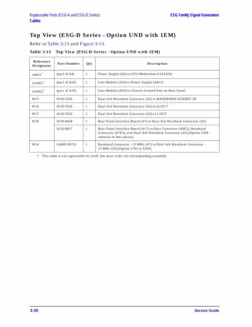
Replaceable Parts (ESG-A and ESG-D Series) ESG Family Signal GeneratorsCables
Top View (ESG-D Series - Option UND with 1EM)Refer to Table 3-13 and Figure 3-13.
Table 3-13 Top View (ESG-D Series - Option UND with 1EM)
Reference Designator
Part Number Qty Description
A4W1*
*. This cable is not replaceable by itself. You must order the corresponding assembly.
(part of A4) 1 Power Supply (A4) to CPU/Motherboard (A14J6)
A16W1* (part of A16) 1 Line Module (A16) to Power Supply (A4J1)
A16W2* (part of A16) 1 Line Module (A16) to Chassis Ground Post on Rear Panel
W15 8120-5556 1 Dual Arb Waveform Generator (A5) to BASEBAND GENREF IN
W16 8120-5556 1 Dual Arb Waveform Generator (A5) to Q OUT
W17 8120-5556 1 Dual Arb Waveform Generator (A5) to I OUT
W18 8120-8458 1 Rear Panel Interface Board (A7) to Dual Arb Waveform Generator (A5)
8120-8457 1 Rear Panel Interface Board (A17) to Data Generator (A8P2), Baseband Generator (A7P2), and Dual Arb Waveform Generator (A5) (Option UN8 - connects in four places)
W24 E4400-20131 1 Baseband Generator - 13 MHz (A7) to Dual Arb Waveform Generator - 13 MHz (A5) (Option UN3 or UN4)
3-30 Service Guide

ESG Family Signal Generators Replaceable Parts (ESG-A and ESG-D Series)Cables
Figure 3-13 Top View (ESG-D Series - Option UND with 1EM)
Service Guide 3-31

Replaceable Parts (ESG-A and ESG-D Series) ESG Family Signal GeneratorsCables
Top View (ESG-D Series - Option 300)Refer to Table 3-14 and Figure 3-14.
Table 3-14 Top View (ESG-D Series - Option 300)
Reference Designator
Part Number Qty Description
W18 8121-0042 1 16-Pin Ribbon Cable, Rear Panel I/O, Rear Panel Interface Board (A17) to Data Generator (A8), Baseband Generator (A7), and Demodulator (A21) (connects in four places)
W19 8121-0040 1 24-Pin Ribbon Cable, BBG I/O, Data Generator (A8) to Demodulator (A21)
W21 8120-5055 1 Flexible Cable, BER GATE IN (RP) to Demodulator (A21)
W22 8120-5055 1 Flexible Cable, BER CLK IN (RP) to Demodulator (A21)
W23 8120-5055 1 Flexible Cable, BER DATA IN (RP) to Demodulator (A21)
W27 8120-8725 1 16-Pin Ribbon Cable, Parallel Data In, Data Generator (A8) to Baseband Generator (A7)
W28 8120-5206 1 Flexible Cable, BERT (A6, BER Gate In) to Demodulator (A21)
W29 8121-0045 1 Flexible Cable, BERT (A6, BER Clk In) to Demodulator (A21)
W30 8120-5014 1 Flexible Cable, BERT (A6, BER Data In) to Demodulator (A21)
W31 8120-8789 1 Ribbon Cable, Motherboard (A14J26) to A20 Down Convertor
W32 8121-0044 1 Flexible Cable, 321.4 MHZ IN (RP) to A20 Down Convertor
W33 8121-0043 1 Flexible Cable, Down Convertor (A20, 26 MHz) to Demodulator (A21, Freq Ref 26 MHz)
W34 8121-0043 1 Flexible Cable, Down Convertor (A20, IF In) to Demodulator (A21, IF In)
A18W1 (part of A18) 1 10-Pin Ribbon Cable, BER Status, BERT Rear Panel Interface (A18) to Data Generator (A8), Baseband Generator (A7), and BERT (A6)
3-32 Service Guide
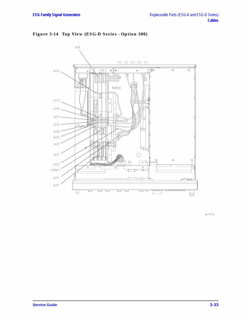
ESG Family Signal Generators Replaceable Parts (ESG-A and ESG-D Series)Cables
Figure 3-14 Top View (ESG-D Series - Option 300)
Service Guide 3-33

Replaceable Parts (ESG-A and ESG-D Series) ESG Family Signal GeneratorsCables
3-34 Service Guide
Inside Front Panel ViewRefer to Table 3-15 and Figure 3-15.
Table 3-15 Inside Front Panel View
NOTE Figure 3-15 shows an ESG-D series front panel having options UN3/4 or UN8. On a standard ESG-D series front panel, W3, W4, and W5 do not exist and the front panel connectors for W1 and W2 will be in a slightly different location. An ESG-A series front panel does not include W1 through W5, but will include W47 with Option 1E6 (not shown). All models having Option 1EM do not have W1 through W9 on the front panel.
Reference Designator
Part Number Qty Description
A1W1*
*. This cable is not replaceable by itself. You must order the corresponding assembly.
(part of A1) 1 Front Panel Board (A1) to CPU/Motherboard (A14J20)
A2DS1W1* (part of A2DS1) 1 Florescent Lamp (A2DS1) to A3W2
A3W1* (part of A3) 1 Inverter (A3) to CPU/Motherboard (A14J19)
A3W2* (part of A3) 1 Inverter (A3) to A2DS1W1
B1W1* (part of B1) 1 Small Fan (B1) to CPU/Motherboard (A14J16)
B2W1* (part of B2) 1 Large Fan (B2) to CPU/Motherboard (A14J17)
W1 8120-6758 1 I IN to Daughterboard (A15J2)
W2 8120-6758 1 Q IN to Daughterboard (A15J3)
W3 8120-5063 1 DATA to Baseband Generator (A7P100) (Options UN3/4)
W4 8120-5063 1 DATA CLOCK to Baseband Generator (A7P103) (Options UN3/4)
W5 8120-5063 1 SYMBOL SYNC to Baseband Generator (A7P101) (Options UN3/4)
W6 8120-6758 1 EXT 1 to Daughterboard (A15J4)
W7 8120-6758 1 EXT 2 to Daughterboard (A15J5)
W8 8120-6758 1 LF OUTPUT to Daughterboard (A15J6)
W9 E4400-20018 1 RF OUTPUT to Electronic Attenuator/RPP (AT1)
E4400-20125 1 RF OUTPUT to RPP (AT1) (Option 1EM, UNB)
W10 8120-6759 1 Display (A2) to CPU/Motherboard (A14J21)
W47 8120-8783 1 Flexible Cable, PULSE IN (FP) to Pulse Modulator (A25) (Option 1E6 - not shown)
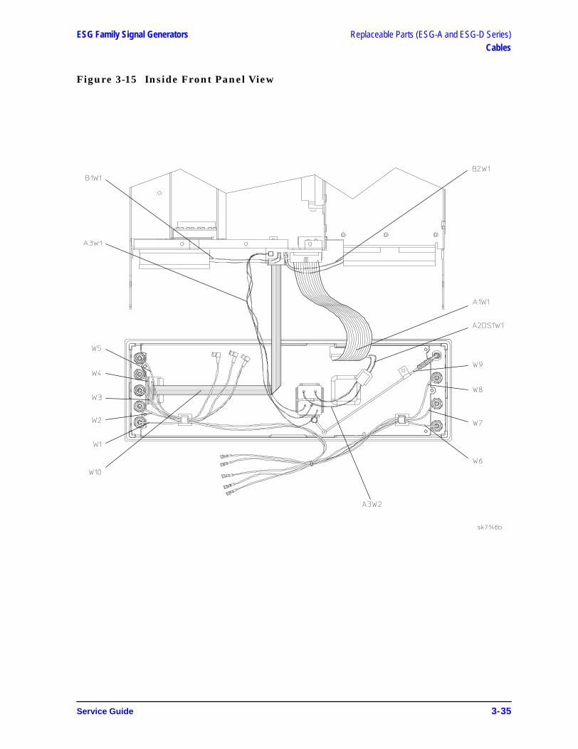
ESG Family Signal Generators Replaceable Parts (ESG-A and ESG-D Series)Cables
Figure 3-15 Inside Front Panel View
Service Guide 3-35
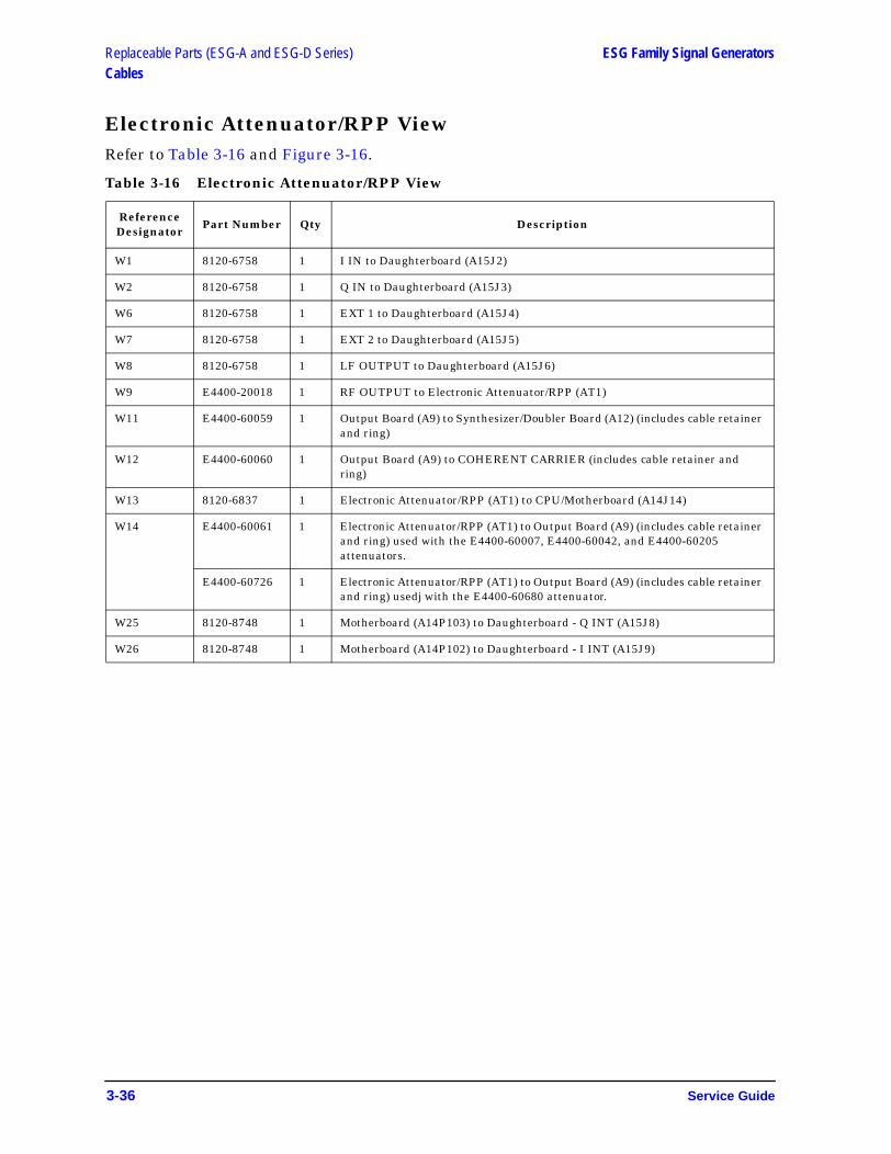
Replaceable Parts (ESG-A and ESG-D Series) ESG Family Signal GeneratorsCables
Electronic Attenuator/RPP ViewRefer to Table 3-16 and Figure 3-16.
Table 3-16 Electronic Attenuator/RPP View
Reference Designator
Part Number Qty Description
W1 8120-6758 1 I IN to Daughterboard (A15J2)
W2 8120-6758 1 Q IN to Daughterboard (A15J3)
W6 8120-6758 1 EXT 1 to Daughterboard (A15J4)
W7 8120-6758 1 EXT 2 to Daughterboard (A15J5)
W8 8120-6758 1 LF OUTPUT to Daughterboard (A15J6)
W9 E4400-20018 1 RF OUTPUT to Electronic Attenuator/RPP (AT1)
W11 E4400-60059 1 Output Board (A9) to Synthesizer/Doubler Board (A12) (includes cable retainer and ring)
W12 E4400-60060 1 Output Board (A9) to COHERENT CARRIER (includes cable retainer and ring)
W13 8120-6837 1 Electronic Attenuator/RPP (AT1) to CPU/Motherboard (A14J14)
W14 E4400-60061 1 Electronic Attenuator/RPP (AT1) to Output Board (A9) (includes cable retainer and ring) used with the E4400-60007, E4400-60042, and E4400-60205 attenuators.
E4400-60726 1 Electronic Attenuator/RPP (AT1) to Output Board (A9) (includes cable retainer and ring) usedj with the E4400-60680 attenuator.
W25 8120-8748 1 Motherboard (A14P103) to Daughterboard - Q INT (A15J8)
W26 8120-8748 1 Motherboard (A14P102) to Daughterboard - I INT (A15J9)
3-36 Service Guide

ESG Family Signal Generators Replaceable Parts (ESG-A and ESG-D Series)Cables
Figure 3-16 Electronic Attenuator/RPP View
Service Guide 3-37

Replaceable Parts (ESG-A and ESG-D Series) ESG Family Signal GeneratorsCables
Electronic Attenuator/RPP View (with Option 1EM)Refer to Table 3-17 and Figure 3-17.
Table 3-17 Electronic Attenuator/RPP View (with Option 1EM)
Reference Designator
Part Number Qty Description
W1 8120-6839 1 I IN to Daughterboard (A15J2)
W2 8120-6839 1 Q IN to Daughterboard (A15J3)
W6 8120-6839 1 EXT 1 to Daughterboard (A15J4)
W7 8120-6839 1 EXT 2 to Daughterboard (A15J5)
W8 8120-6839 1 LF OUTPUT to Daughterboard (A15J6)
W9 E4400-20025 1 RF OUTPUT to Electronic Attenuator/RPP (AT1)
W11 E4400-60059 1 Output Board (A9) to Synthesizer/Doubler Board (A12) (includes cable retainer and ring)
W12 E4400-60060 1 Output Board (A9) to COHERENT CARRIER (includes cable retainer and ring)
W13 8120-6837 1 Electronic Attenuator/RPP (AT1) to CPU/Motherboard (A14J14)
W14 E4400-60061 1 Electronic Attenuator/RPP (AT1) to Output Board (A9) (includes cable retainer and ring) used with the E4400-60007, E4400-60042, and E4400-60205 attenuators.
W14 E4400-60726 1 Electronic Attenuator/RPP (AT1) to Output Board (A9) (includes cable retainer and ring) used with the E4400-60680 attenuator.
W25 8120-8748 1 Motherboard (A14P103) to Daughterboard - Q INT (A15J8)
W26 8120-8748 1 Motherboard (A14P102) to Daughterboard - I INT (A15J9)
3-38 Service Guide

ESG Family Signal Generators Replaceable Parts (ESG-A and ESG-D Series)Cables
Figure 3-17 Electronic Attenuator/RPP View (with Option 1EM)
Service Guide 3-39

Replaceable Parts (ESG-A and ESG-D Series) ESG Family Signal GeneratorsCables
Mechanical Attenuator View (Option UNB)Refer to Table 3-18 and Figure 3-18.
Table 3-18 Mechanical Attenuator View (Option UNB)
Reference Designator
Part Number Qty Description
A19W1*
*. This cable is not replaceable by itself. You must order the corresponding assembly.
(part of A19) 1 RPP (A19) to Motherboard (A14J15)
W1 8120-6839 1 I IN to Daughterboard (A15J2)
W2 8120-6839 1 Q IN to Daughterboard (A15J3)
W6 8120-6758 1 EXT 1 to Daughterboard (A15J4)
W7 8120-6758 1 EXT 2 to Daughterboard (A15J5)
W8 8120-6758 1 LF OUTPUT to Daughterboard (A15J6)
W9 E4400-20125 1 RF OUTPUT to RPP (A19)
W11 E4400-60059 1 Output Board (A9) to Synthesizer/Doubler Board (A12) (includes cable retainer and ring)
W12 E4400-60176 1 Output Board (A9) to COHERENT CARRIER (includes cable retainer and ring)
W13 E4400-20132 1 Mechanical Attenuator (AT1) to CPU/Motherboard (A14J14)
W14 E4400-60177 1 Mechanical Attenuator (AT1) to Output Board (A9) (includes cable retainer and ring)
W20 E4400-20126 1 Mechanical Attenuator (AT1) to RPP (A19)
W25 8120-8748 1 Motherboard (A14P103) to Daughterboard - Q INT (A15J8)
W26 8120-8748 1 Motherboard (A14P102) to Daughterboard - I INT (A15J9)
3-40 Service Guide

ESG Family Signal Generators Replaceable Parts (ESG-A and ESG-D Series)Cables
Figure 3-18 Mechanical Attenuator View (Option UNB)
Service Guide 3-41
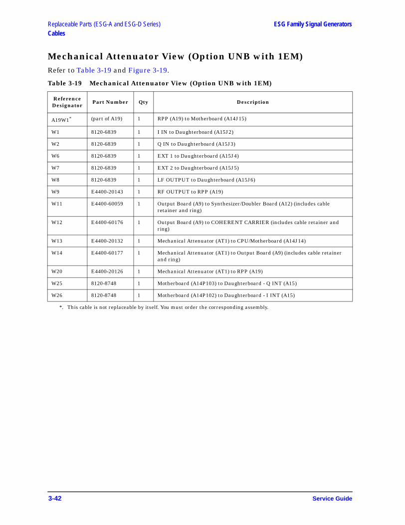
Replaceable Parts (ESG-A and ESG-D Series) ESG Family Signal GeneratorsCables
Mechanical Attenuator View (Option UNB with 1EM)Refer to Table 3-19 and Figure 3-19.
Table 3-19 Mechanical Attenuator View (Option UNB with 1EM)
Reference Designator
Part Number Qty Description
A19W1*
*. This cable is not replaceable by itself. You must order the corresponding assembly.
(part of A19) 1 RPP (A19) to Motherboard (A14J15)
W1 8120-6839 1 I IN to Daughterboard (A15J2)
W2 8120-6839 1 Q IN to Daughterboard (A15J3)
W6 8120-6839 1 EXT 1 to Daughterboard (A15J4)
W7 8120-6839 1 EXT 2 to Daughterboard (A15J5)
W8 8120-6839 1 LF OUTPUT to Daughterboard (A15J6)
W9 E4400-20143 1 RF OUTPUT to RPP (A19)
W11 E4400-60059 1 Output Board (A9) to Synthesizer/Doubler Board (A12) (includes cable retainer and ring)
W12 E4400-60176 1 Output Board (A9) to COHERENT CARRIER (includes cable retainer and ring)
W13 E4400-20132 1 Mechanical Attenuator (AT1) to CPU/Motherboard (A14J14)
W14 E4400-60177 1 Mechanical Attenuator (AT1) to Output Board (A9) (includes cable retainer and ring)
W20 E4400-20126 1 Mechanical Attenuator (AT1) to RPP (A19)
W25 8120-8748 1 Motherboard (A14P103) to Daughterboard - Q INT (A15)
W26 8120-8748 1 Motherboard (A14P102) to Daughterboard - I INT (A15)
3-42 Service Guide

ESG Family Signal Generators Replaceable Parts (ESG-A and ESG-D Series)Cables
Figure 3-19 Mechanical Attenuator View (Option UNB with 1EM)
Service Guide 3-43
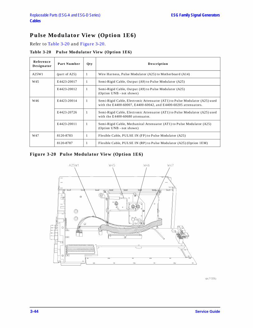
Replaceable Parts (ESG-A and ESG-D Series) ESG Family Signal GeneratorsCables
Pulse Modulator View (Option 1E6)Refer to Table 3-20 and Figure 3-20.
Table 3-20 Pulse Modulator View (Option 1E6)
Figure 3-20 Pulse Modulator View (Option 1E6)
Reference Designator
Part Number Qty Description
A25W1 (part of A25) 1 Wire Harness, Pulse Modulator (A25) to Motherboard (A14)
W45 E4423-20017 1 Semi-Rigid Cable, Output (A9) to Pulse Modulator (A25)
E4423-20012 1 Semi-Rigid Cable, Output (A9) to Pulse Modulator (A25)(Option UNB - not shown)
W46 E4423-20014 1 Semi-Rigid Cable, Electronic Attenuator (AT1) to Pulse Modulator (A25) used with the E4400-60007, E4400-60042, and E4400-60205 attenuators.
E4423-20726 1 Semi-Rigid Cable, Electronic Attenuator (AT1) to Pulse Modulator (A25) used with the E4400-60680 attenuator.
E4423-20011 1 Semi-Rigid Cable, Mechanical Attenuator (AT1) to Pulse Modulator (A25) (Option UNB - not shown)
W47 8120-8783 1 Flexible Cable, PULSE IN (FP) to Pulse Modulator (A25)
8120-8787 1 Flexible Cable, PULSE IN (RP) to Pulse Modulator (A25) (Option 1EM)
3-44 Service Guide

ESG Family Signal Generators Replaceable Parts (ESG-A and ESG-D Series)Hardware and Other Instrument Parts
Hardware and Other Instrument PartsThis section lists part numbers for hardware and other parts in your signal generator. Thefollowing instrument views are provided to help you locate specific parts.
• “Top View” on page 3-46
• “Downconvertor View (Option 300)” on page 3-48
• “Disassembled Mechanical Attenuator View (Option UNB)” on page 3-49
• “Disassembled Pulse Modulator View (Option 1E6)” on page 3-50
• “Disassembled Pulse Modulator View (Option 1E6/UNB)” on page 3-51
• “Front Panel View (ESG-A Series)” on page 3-52
• “Front Panel View (ESG-D Series)” on page 3-54
• “Disassembled Front-Panel View” on page 3-56
• “Daughterboard Card Cage View” on page 3-58
• “Inside Rear-Panel View” on page 3-59
• “Rear-Panel View (ESG-A Series)” on page 3-60
• “Rear-Panel View (ESG-A Series - Option 1EM)” on page 3-62
• “Rear-Panel View (ESG-D Series)” on page 3-64
• “Rear Panel View (ESG-D Series - Option 1EM)” on page 3-66
• “Instrument Chassis with Top and Right-Side Hardware” on page 3-68
• “Power Supply Shield and Left-Side Hardware” on page 3-70
• “Motherboard and Bottom-Side Hardware” on page 3-71
• “Instrument Cover and Associated Parts” on page 3-72
Service Guide 3-45

Replaceable Parts (ESG-A and ESG-D Series) ESG Family Signal GeneratorsHardware and Other Instrument Parts
Top ViewRefer to Table 3-21 and Figure 3-21.
Table 3-21 Top View
Item No. Part Number Qty Description
1 1400-0054 1 Clamp-Semi-Rigid Cable (W14)
2 0515-0372 1 Screw-Machine M3x8 CW-PN-TX
3 0515-0430 2 Screw-Machine M3x6 CW-PN-TX
4 1400-1594 1 Clamp-Flexible Cables (not used on Option 1EM)
5 0361-1341 4 Rivet-Plastic
6 0515-0374 4 Screw-Machine M3x10 CW-PN-TX
7 E4400-20041 1 Shield Cap
8 0400-0001 1 Grommet Round .562ID
9 0515-1521 2 Screw-Machine M3x5 FL-TX
10 E4400-60221 1 A14Q501 Transistor Assembly
11 0515-0374 1 Screw-Machine M3x10 CW-PN-TX
12 0340-1162 1 Bushing, Insulator 0.119 ID
13 0340-0614 1 Insulator Pad, Transistor TO-220
3-46 Service Guide
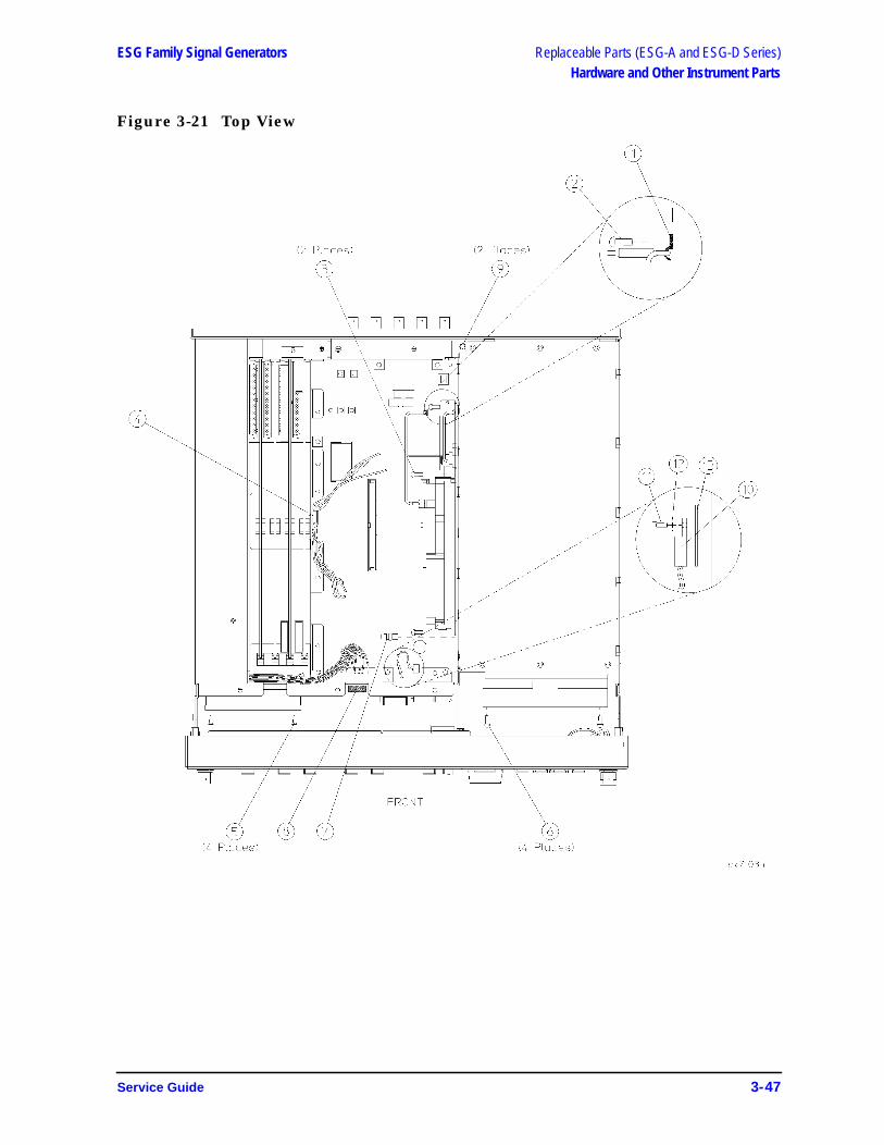
ESG Family Signal Generators Replaceable Parts (ESG-A and ESG-D Series)Hardware and Other Instrument Parts
Figure 3-21 Top View
Service Guide 3-47

Replaceable Parts (ESG-A and ESG-D Series) ESG Family Signal GeneratorsHardware and Other Instrument Parts
Downconvertor View (Option 300)Refer to Table 3-22 and Figure 3-22.
Table 3-22 Downconvertor View
Figure 3-22 Downconvertor View
Item No. Part Number Qty Description
1 0515-0372 2 Screw-Machine M3x8 CW-PN-TX
3-48 Service Guide

ESG Family Signal Generators Replaceable Parts (ESG-A and ESG-D Series)Hardware and Other Instrument Parts
Disassembled Mechanical Attenuator View (Option UNB)Refer to Table 3-23 and Figure 3-23.
Table 3-23 Disassembled Mechanical Attenuator View
Figure 3-23 Disassembled Mechanical Attenuator View
Item No. Part Number Qty Description
1 E4400-00027 1 Bracket-RPP
2 0515-0664 3 Screw-Machine M3x12 CW-PN-TX
3 0515-0430 2 Screw-Machine M3x6 CW-PN-TX
4 E4400-00028 1 Bracket-Attenuator
5 0515-1102 6 Screw-Machine M3x8 FL-TX
Service Guide 3-49

Replaceable Parts (ESG-A and ESG-D Series) ESG Family Signal GeneratorsHardware and Other Instrument Parts
Disassembled Pulse Modulator View (Option 1E6)Refer to Table 3-24 and Figure 3-24.
Table 3-24 Disassembled Pulse Modulator View (Option 1E6)
Figure 3-24 Disassembled Pulse Modulator View (Option 1E6)
Item No. Part Number Qty Description
1 0515-0372 2 Screw-Machine M3x8 CW-PN-TX
2 E4423-00003 1 Bracket-Pulse Modulator
3 0515-2001 2 Screw-Machine M2.5x10 FL-TX
3-50 Service Guide

ESG Family Signal Generators Replaceable Parts (ESG-A and ESG-D Series)Hardware and Other Instrument Parts
Disassembled Pulse Modulator View (Option 1E6/UNB)Refer to Table 3-25 and Figure 3-25.
Table 3-25 Disassembled Pulse Modulator View (Option 1E6/UNB)
Figure 3-25 Disassembled Pulse Modulator View (Option 1E6/UNB)
Item No. Part Number Qty Description
1 E4400-00027 1 Bracket-RPP
2 0515-0664 3 Screw-Machine M3x12 CW-PN-TX
3 0515-0430 2 Screw-Machine M3x6 CW-PN-TX
4 E4400-00028 1 Bracket-Attenuator
5 0515-1102 6 Screw-Machine M3x8 FL-TX
6 0515-0367 2 Screw-Machine M2.5x8 CW-PN-TX
Service Guide 3-51
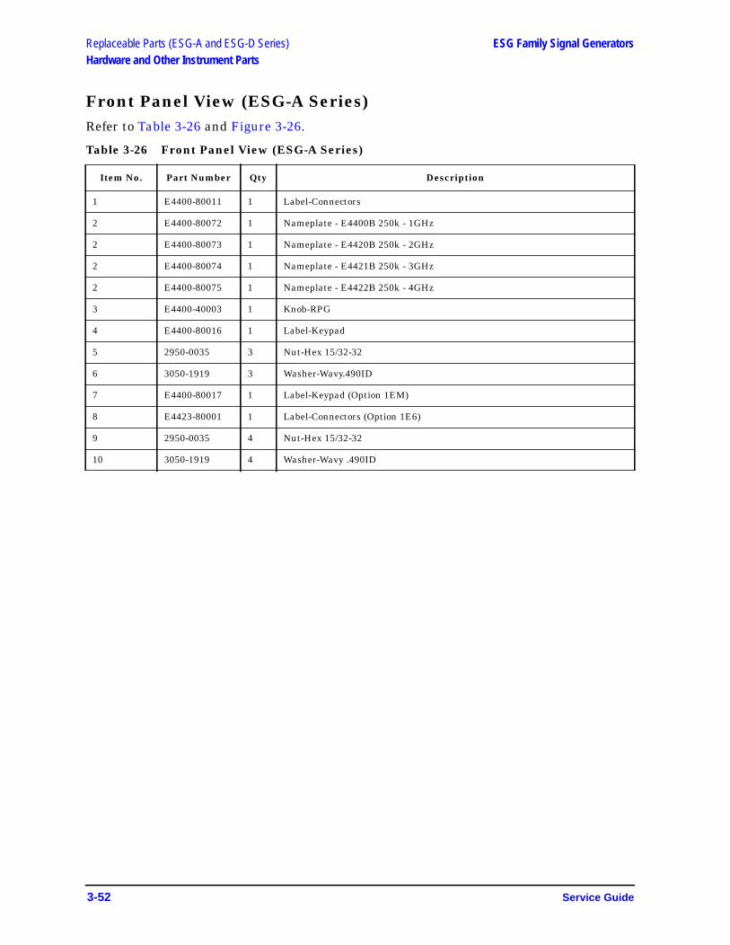
Replaceable Parts (ESG-A and ESG-D Series) ESG Family Signal GeneratorsHardware and Other Instrument Parts
Front Panel View (ESG-A Series)Refer to Table 3-26 and Figure 3-26.
Table 3-26 Front Panel View (ESG-A Series)
Item No. Part Number Qty Description
1 E4400-80011 1 Label-Connectors
2 E4400-80072 1 Nameplate - E4400B 250k - 1GHz
2 E4400-80073 1 Nameplate - E4420B 250k - 2GHz
2 E4400-80074 1 Nameplate - E4421B 250k - 3GHz
2 E4400-80075 1 Nameplate - E4422B 250k - 4GHz
3 E4400-40003 1 Knob-RPG
4 E4400-80016 1 Label-Keypad
5 2950-0035 3 Nut-Hex 15/32-32
6 3050-1919 3 Washer-Wavy.490ID
7 E4400-80017 1 Label-Keypad (Option 1EM)
8 E4423-80001 1 Label-Connectors (Option 1E6)
9 2950-0035 4 Nut-Hex 15/32-32
10 3050-1919 4 Washer-Wavy .490ID
3-52 Service Guide

ESG Family Signal Generators Replaceable Parts (ESG-A and ESG-D Series)Hardware and Other Instrument Parts
Figure 3-26 Front Panel View (ESG-A Series)
Service Guide 3-53

Replaceable Parts (ESG-A and ESG-D Series) ESG Family Signal GeneratorsHardware and Other Instrument Parts
Front Panel View (ESG-D Series)Refer to Table 3-27 and Figure 3-27.
Table 3-27 Front Panel View (ESG-D Series)
Item No. Part Number Qty Description
1 E4400-80010 1 Label-Connectors
2 E4400-80076 1 Nameplate - E4430B 250k - 1GHz
2 E4400-80077 1 Nameplate - E4431B 250k - 2GHz
2 E4400-80078 1 Nameplate - E4432B 250k - 3GHz
2 E4400-80079 1 Nameplate - E4433B 250k - 4GHz
3 E4400-40003 1 Knob-RPG
4 E4400-80005 1 Label-Keypad
5 2950-0035 5 Nut-Hex 15/32-32
6 3050-1919 5 Washer-Wavy .490ID
7 E4400-80011 1 Label-Connectors (Option 1EM)
8 E4400-80015 1 Label-Keypad (Option 1EM)
9 E4400-80006 1 Label-Connectors (Options UN3, UN4, UN7, UN8, UND)
10 2950-0035 8 Nut-Hex 15/32-32 (Options UN3, UN4, UN7, UN8, UND)
11 3050-1919 8 Washer-Wavy .490ID (Options UN3, UN4, UN7, UN8, UND)
3-54 Service Guide
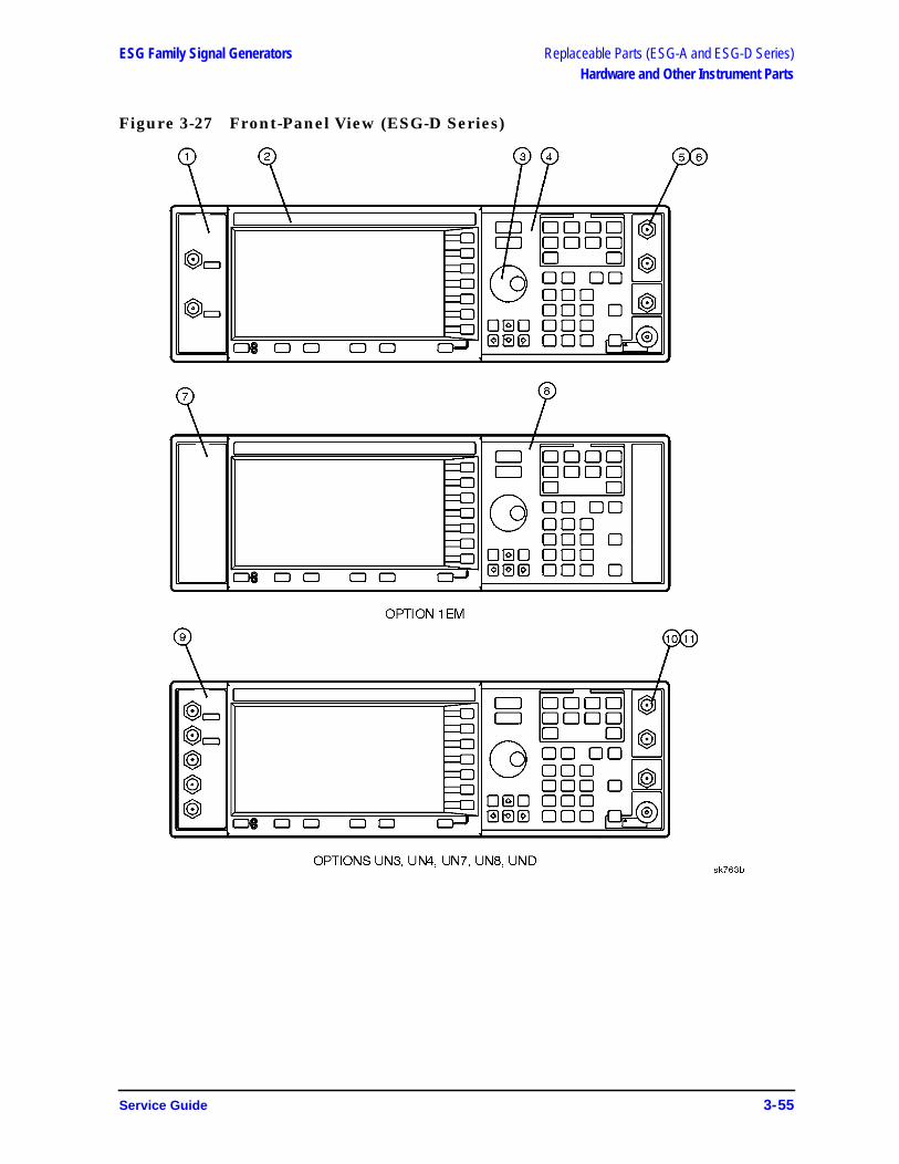
ESG Family Signal Generators Replaceable Parts (ESG-A and ESG-D Series)Hardware and Other Instrument Parts
Figure 3-27 Front-Panel View (ESG-D Series)
Service Guide 3-55
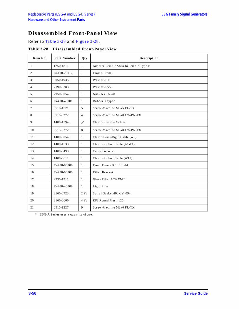
Replaceable Parts (ESG-A and ESG-D Series) ESG Family Signal GeneratorsHardware and Other Instrument Parts
Disassembled Front-Panel ViewRefer to Table 3-28 and Figure 3-28.
Table 3-28 Disassembled Front-Panel View
Item No. Part Number Qty Description
1 1250-1811 1 Adapter-Female SMA to Female Type-N
2 E4400-20012 1 Frame-Front
3 3050-1935 1 Washer-Flat
4 2190-0383 1 Washer-Lock
5 2950-0054 1 Nut-Hex 1/2-28
6 E4400-40001 1 Rubber Keypad
7 0515-1521 5 Screw-Machine M3x5 FL-TX
8 0515-0372 4 Screw-Machine M3x8 CW-PN-TX
9 1400-1594 2*
*. ESG-A Series uses a quantity of one.
Clamp-Flexible Cables
10 0515-0372 8 Screw-Machine M3x8 CW-PN-TX
11 1400-0054 1 Clamp-Semi-Rigid Cable (W9)
12 1400-1533 1 Clamp-Ribbon Cable (A1W1)
13 1400-0493 1 Cable Tie Wrap
14 1400-0611 1 Clamp-Ribbon Cable (W10)
15 E4400-00008 1 Front Frame RFI Shield
16 E4400-00009 1 Filter Bracket
17 4330-1711 1 Glass Filter 70% XMT
18 E4400-40008 1 Light Pipe
19 8160-0723 2 Ft Spiral Gasket-BC CY .094
20 8160-0660 4 Ft RFI Round Mesh.125
21 0515-1227 9 Screw-Machine M3x6 FL-TX
3-56 Service Guide
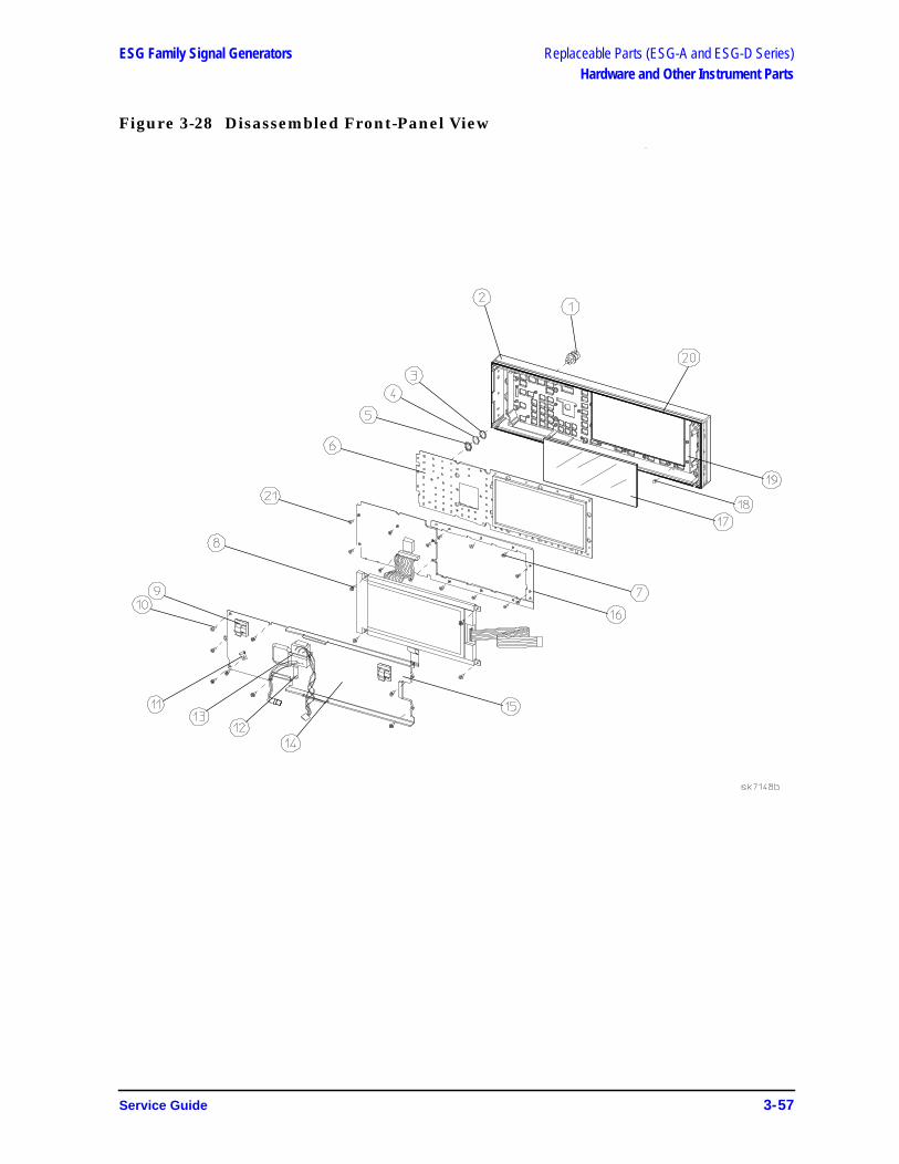
ESG Family Signal Generators Replaceable Parts (ESG-A and ESG-D Series)Hardware and Other Instrument Parts
Figure 3-28 Disassembled Front-Panel View
Service Guide 3-57

Replaceable Parts (ESG-A and ESG-D Series) ESG Family Signal GeneratorsHardware and Other Instrument Parts
Daughterboard Card Cage ViewRefer to Table 3-29 and Figure 3-29.
Table 3-29 Daughterboard Card Cage View
Figure 3-29 Daughterboard Card Cage View
Item No. Part Number Qty Description
1 E4400-40002 4 Retainer-Cable
2 0510-1643 4 Retainer Ring .309ID
3 0515-0430 5 Screw-Machine M3x6 CW-PN-TX
3-58 Service Guide

ESG Family Signal Generators Replaceable Parts (ESG-A and ESG-D Series)Hardware and Other Instrument Parts
Inside Rear-Panel ViewRefer to Table 3-30 and Figure 3-30.
Table 3-30 Inside Rear-Panel View
Figure 3-30 Inside Rear-Panel View
Item No. Part Number Qty Description
1 0535-0031 2 Nut-Hex M3.0
Service Guide 3-59

Replaceable Parts (ESG-A and ESG-D Series) ESG Family Signal GeneratorsHardware and Other Instrument Parts
Rear-Panel View (ESG-A Series)Refer to Table 3-31 and Figure 3-31.
Table 3-31 Rear-Panel View (ESG-A Series)
Item No. Part Number Qty Description
1 0515-0372 10 Screw-Machine M3x8 CW-PN-TX
2 E4400-00032 1 Panel-Rear
6 6960-0023 1 Plug-Hole .312D
7 E4400-00017 1 Serial Number Plate
8 0515-1102 2 Screw-Machine M3x8 FL-TX
9 0380-0644 2 Standoff-Hex .327L 6-32
10 2190-0577 2 Washer-Lock
11 0380-2079 2 Standoff-Hex .312L 4-40
12 2190-0003 2 Washer-Lock
14 2950-0054 5 Nut-Hex 1/2-28
15 2190-0068 5 Washer-Lock .505ID
3-60 Service Guide
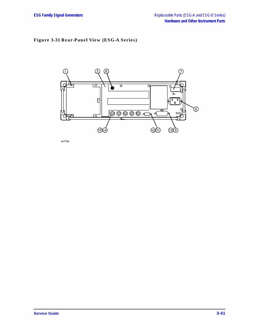
ESG Family Signal Generators Replaceable Parts (ESG-A and ESG-D Series)Hardware and Other Instrument Parts
Figure 3-31 Rear-Panel View (ESG-A Series)
Service Guide 3-61

Replaceable Parts (ESG-A and ESG-D Series) ESG Family Signal GeneratorsHardware and Other Instrument Parts
Rear-Panel View (ESG-A Series - Option 1EM)Refer to Table 3-32 and Figure 3-32.
Table 3-32 Rear-Panel View (ESG-A Series - Option 1EM)
Item No. Part Number Qty Description
1 0515-0372 10 Screw-Machine M3x8 CW-PN-TX
2 E4400-00033 1 Panel-Rear
6 6960-0023 1 Plug-Hole .312D
7 2950-0035 3*
*. For Option 1E6 quantity is 4.
Nut-Hex 15/32-32
8 2190-0102 3* Washer-Lock .472ID
9 08559-60002 1 RF Output Assy
10 2950-0132 1 Nut-Hex 7/16-28
11 2190-0102 1 Washer-Lock
12 6960-0002 2†
†. For Option 1E6 quantity is 1.
Plug-Hole .500D
13 E4400-00017 1 Serial Number Plate
14 0515-1102 2 Screw-Machine M3x8 FL-TX
15 0380-0644 2 Standoff-Hex .327L 6-32
16 2190-0577 2 Washer-Lock
17 0380-2079 2 Standoff-Hex .312L 4-40
18 2190-0003 2 Washer-Lock
19 2950-0054 5 Nut-Hex 1/2-28
20 2190-0068 5 Washer-Lock .505ID
3-62 Service Guide

ESG Family Signal Generators Replaceable Parts (ESG-A and ESG-D Series)Hardware and Other Instrument Parts
Figure 3-32 Rear-Panel View (ESG-A Series - Option 1EM)
Service Guide 3-63
Replaceable Parts (ESG-A and ESG-D Series) ESG Family Signal GeneratorsHardware and Other Instrument Parts
Rear-Panel View (ESG-D Series)Refer to Table 3-33 and Figure 3-33.
Table 3-33 Rear-Panel View (ESG-D Series)
Item No. Part Number Qty Description
1 0515-0372 10 Screw-Machine M3x8 CW-PN-TX
2 E4400-00032 1 Panel-Rear
3 0515-0372 1 Screw-Machine M3x8 CW-PN-TX (used to attach item 4))
4 1250-2759 1 Dust Cap Female SMA
5 1250-1753 1 Adapter-Female SMA to Female SMA
7 E4400-00017 1 Serial Number Plate
8 0515-1102 2 Screw-Machine M3x8 FL-TX
9 0380-0644 2 Standoff-Hex .327L 6-32
10 2190-0577 2 Washer-Lock
11 0380-2079 2 Standoff-Hex .312L 4-40
12 2190-0003 2 Washer-Lock
13 6960-0002 3 Plug-Hole .500D (Options UN3, UN4, UN8, UND)
14 2950-0054 5 Nut-Hex 1/2-28
15 2190-0068 5 Washer-Lock .505ID
16 2950-0035 11 Nut-Hex 15/32-32 (Options UN3, UN4, UN8, UND)
17 2190-0102 11 Washer-Lock .472ID (Options UN3, UN4, UN8, UND)
18 E4400-00031 1 Panel-Rear (Options UN3, UN4. UN8, UND)
19 2950-0035 14 Nut-Hex 15/32-32 (Option UN7)
20 2190-0102 14 Washer-Lock .472ID (Option UN7)
21 E4400-00025 1 Panel-Rear (Option UN7)
22 2950-0078 5 Nut-Hex 10-32 (for the SMBs) (Option UN7)
23 2190-0124 5 Washer-Lock .195ID (for the SMBs) (Option UN7)
24 2950-0078 6 Nut-Hex 10-32 (for the SMBs) (Option 300)
25 2190-0124 6 Washer-Lock .195ID (for the SMBs) (Option 300)
26 E4400-00025 1 Panel-Rear (Option 300)
3-64 Service Guide

ESG Family Signal Generators Replaceable Parts (ESG-A and ESG-D Series)Hardware and Other Instrument Parts
Figure 3-33 Rear-Panel View (ESG-D Series)
Service Guide 3-65

Replaceable Parts (ESG-A and ESG-D Series) ESG Family Signal GeneratorsHardware and Other Instrument Parts
Rear Panel View (ESG-D Series - Option 1EM)Refer to Table 3-34 and Figure 3-34.
Table 3-34 Rear Panel View (ESG-D Series - Option 1EM)
Item No. Part Number Qty Description
1 0515-0372 10 Screw-Machine M3x8 CW-PN-TX
2 E4400-00033 1 Panel-Rear
3 0515-0372 1 Screw-Machine M3x8 CW-PN-TX (used to attach item 4)
4 1250-2759 1 Dust Cap Female SMA
5 1250-1753 1 Adapter-Female SMA to Female SMA
7 2950-0035 5 Nut-Hex 15/32-32
8 2190-0102 5 Washer-Lock .472ID
9 08559-60002 1 RF Output Assy
10 2950-0132 1 Nut-Hex 7/16-28
11 2190-0102 1 Washer-Lock
13 E4400-00017 1 Serial Number Plate
14 0515-1102 2 Screw-Machine M3x8 FL-TX
15 0380-0644 2 Standoff-Hex .327L 6-32
16 2190-0577 2 Washer-Lock
17 0380-2079 2 Standoff-Hex .312L 4-40
18 2190-0003 2 Washer-Lock
19 2950-0054 5 Nut-Hex 1/2-28
20 2190-0068 5 Washer-Lock .505ID
21 E4400-00034 1 Panel-Rear (Options UN3, UN4, UN8)
22 2950-0078 14 Nut-Hex 10-32 (for the SMBs) (Options UN3, UN4, UN8, UND)
23 2190-0124 14 Washer-Lock .195ID (for the SMBs) (Options UN3, UN4, UN8, UND)
24 E4400-00026 1 Panel-Rear (Option UN7)
25 2950-0078 22 Nut-Hex 10-32 (for the SMBs) (Option UN7)
26 2190-0124 22 Washer-Lock .195ID (for the SMBs) (Option UN7)
27 E4400-00026 1 Panel-Rear (Option 300)
28 2950-0078 22 Nut-Hex 10-32 (for the SMBs) (Option UN7)
29 2190-0124 14 Washer-Lock .195ID (for the SMBs) (Options UN3, UN4, UN8, UND)
3-66 Service Guide

ESG Family Signal Generators Replaceable Parts (ESG-A and ESG-D Series)Hardware and Other Instrument Parts
Figure 3-34 Rear-Panel View (ESG-D Series - Option 1EM)
Service Guide 3-67

Replaceable Parts (ESG-A and ESG-D Series) ESG Family Signal GeneratorsHardware and Other Instrument Parts
Instrument Chassis with Top and Right-Side HardwareRefer to Table 3-35 and Figure 3-35.
Table 3-35 Instrument Chassis with Top and Right-Side Hardware
Item No. Part Number Qty Description
1 0515-1269 2 Screw-Machine M4X10 FL-TX
2 0515-2087 4 Screw-Machine M3x6 CW-BN-TX
3 E4400-00003 1 Cover-Side (Serial Prefix US3833, or GB3832, and below)
3 E4400-00037 1 Cover-Side (Serial Prefix US3844, or GB3845, and above)
4 E4400-00035 1 Chassis
5 E4400-00036 1 Cover-Top Chassis
6 0515-0430 11 Screw-Machine M3x6 CW-PN-TX
7 E4400-80066 1 Label-Connection Diagram
3-68 Service Guide

ESG Family Signal Generators Replaceable Parts (ESG-A and ESG-D Series)Hardware and Other Instrument Parts
Figure 3-35 Instrument Chassis with Top and Right-Side Hardware
Service Guide 3-69
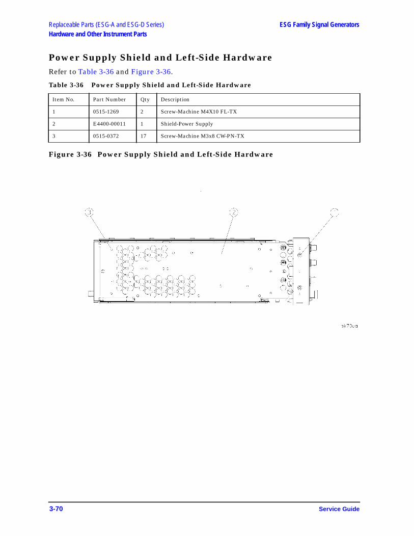
Replaceable Parts (ESG-A and ESG-D Series) ESG Family Signal GeneratorsHardware and Other Instrument Parts
Power Supply Shield and Left-Side HardwareRefer to Table 3-36 and Figure 3-36.
Table 3-36 Power Supply Shield and Left-Side Hardware
Figure 3-36 Power Supply Shield and Left-Side Hardware
Item No. Part Number Qty Description
1 0515-1269 2 Screw-Machine M4X10 FL-TX
2 E4400-00011 1 Shield-Power Supply
3 0515-0372 17 Screw-Machine M3x8 CW-PN-TX
3-70 Service Guide

ESG Family Signal Generators Replaceable Parts (ESG-A and ESG-D Series)Hardware and Other Instrument Parts
Motherboard and Bottom-Side HardwareRefer to Table 3-37 and Figure 3-37.
Table 3-37 Motherboard and Bottom-Side Hardware
Figure 3-37 Motherboard and Bottom-Side Hardware
Item No. Part Number Qty Description
1 0515-0372 15 Screw-Machine M3x8 CW-PN-TX
2 E4400-00007 1 Cover-Bottom Chassis
3 0515-0372 2 Screw-Machine M3x8 CW-PN-TX
Service Guide 3-71

Replaceable Parts (ESG-A and ESG-D Series) ESG Family Signal GeneratorsHardware and Other Instrument Parts
Instrument Cover and Associated PartsRefer to Table 3-38 and Figure 3-38.
Table 3-38 Instrument Cover and Associated Parts
Item No. Part Number Qty Description
1 0515-1619 4 Screw-Machine M4x25 PN-TX
2 5041-9611 4 Foot-Rear Long
3 5041-9167 4 Feet-Bottom
4 1460-1345 2 Spring-Wire Frame 3.000 Long
5 5041-9171 2 Side Trim
6 E4400-60026 2 Assy-Strap Handle - includes the following parts:
Item 6includesthese parts:
5063-9209 1 Strap Assembly
E4400-00015 2 Ground Spring
E4400-20023 2 Handle Retainer
E4400-40007 2 End Cap
0515-0710 2 Screw-Machine M5x18 FL-TX
7 E4400-00004 1 Cover-Instrument
3-72 Service Guide

ESG Family Signal Generators Replaceable Parts (ESG-A and ESG-D Series)Hardware and Other Instrument Parts
Figure 3-38 Instrument Cover and Associated Parts
Service Guide 3-73

Replaceable Parts (ESG-A and ESG-D Series) ESG Family Signal GeneratorsMiscellaneous
MiscellaneousThis section lists part numbers for miscellaneous items that can be used with your signalgenerator. These items are categorized as follows:
• “Accessories” on page 3-74
• “Documentation” on page 3-75
• “Electrostatic Discharge (ESD) Protective Supplies” on page 3-78
• “Upgrade and Retrofit Kits” on page 3-78
AccessoriesRefer to Table 3-39.
Table 3-39 Accessories
Description Part Number
Connector End Cap-RF Output 1401-0247
Connector End Cap-GPIB 1401-5007
Connector End Cap Coherent Carrier Out 1252-4696
Remote Interface 83300A
Transit Case 9211-1296
3-74 Service Guide

ESG Family Signal Generators Replaceable Parts (ESG-A and ESG-D Series)Miscellaneous
DocumentationRefer to Table 3-40 and Table 3-41.
Table 3-40 ESG Family Signal Generators Documentation
Description Part Number
ESG-A and ESG-AP Series Manual Set (includes items listed below) E4400-90334
User’s Guide E4400-90323
Programming Guide E4400-90324
Calibration Guide E4400-90325
Quick Start Guide E4400-90326
Error Messages E4400-90333
Technical Specifications 5965-3096E
Feature Releases Document E4400-90363
ESG-D and ESG-DP Series Manual Set (includes items listed below) E4400-90322
User’s Guide E4400-90323
Programming Guide E4400-90324
Calibration Guide E4400-90325
Quick Start Guide E4400-90326
Error Messages E4400-90333
Technical Specifications 5965-3096E
Feature Releases Document E4400-90363
Option 200 Fully Coded 3GPP W-CDMA Personality User’s and Programming Guide E4400-90390
Option 201 Real-Time cdma2000 Personality User’s and Programming Guide E4400-90386
Option UN8 Real-Time I/Q Baseband Generator with TDMA Standards User’s andProgramming Guide (includes Option 202, EDGE)
E4400-90327
Option UND Dual Arbitrary Waveform Generator and Option UN5 Multichannel,Multicarrier CDMA Personality User’s and Programming Guide
E4400-90328
Option 100 W-CDMA Personality User’s and Programming Guide E4400-90329
Option 101 CDMA2000 Personality User’s and Programming Guide E4400-90330
Option UN7 Bit Error Rate Test User’s and Programming Guide E4400-90331
Option 300 Base Station BERT Extension for Option UN7 User’s and ProgrammingGuide
E4400-90305
Service Guide E4400-90335
Component-Level Information E4400-90336
Service Guide 3-75

Replaceable Parts (ESG-A and ESG-D Series) ESG Family Signal GeneratorsMiscellaneous
Table 3-41 Localized Documentation for ESG Family Signal Generators
Description Part Number
Chinese
User’s Guide - Chinese E4400-90172
Option UN8 DECT User’s and Programming Guide - Chinese E4400-90194
Option UN8 GSM User’s and Programming Guide - Chinese E4400-90201
Option UN8 Custom Digital Modulation User’s and Programming Guide - Chinese E4400-90180
Option UND Dual Arbitrary Waveform Generator and Option UN5 Multichannel,Multicarrier CDMA Personality User’s and Programming Guide - Chinese
E4400-90187
Taiwanese
User’s Guide - Taiwanese E4400-90173
Option UN8 DECT User’s and Programming Guide - Taiwanese E4400-90195
Option UN8 GSM User’s and Programming Guide - Taiwanese E4400-90202
Option UN8 Custom Digital Modulation User’s and Programming Guide - Taiwanese E4400-90181
Option UND Dual Arbitrary Waveform Generator and Option UN5 Multichannel,Multicarrier CDMA Personality User’s and Programming Guide - Taiwanese
E4400-90188
French
User’s Guide - French E4400-90174
Option UN8 DECT User’s and Programming Guide - French E4400-90196
Option UN8 GSM User’s and Programming Guide - French E4400-90203
Option UN8 TETRA User’s and Programming Guide - French E4400-90212
Option UN8 Custom Digital Modulation User’s and Programming Guide - French E4400-90182
Option UND Dual Arbitrary Waveform Generator and Option UN5 Multichannel,Multicarrier CDMA Personality User’s and Programming Guide - French
E4400-90189
German
User’s Guide - German E4400-90175
Option UN8 DECT User’s and Programming Guide - German E4400-90197
Option UN8 GSM User’s and Programming Guide - German E4400-90204
Option UN8 TETRA User’s and Programming Guide - German E4400-90210
Option UN8 Custom Digital Modulation User’s and Programming Guide - German E4400-90183
Option UND Dual Arbitrary Waveform Generator and Option UN5 Multichannel,Multicarrier CDMA Personality User’s and Programming Guide - German
E4400-90190
3-76 Service Guide

ESG Family Signal Generators Replaceable Parts (ESG-A and ESG-D Series)Miscellaneous
Japanese
User’s Guide - Japanese E4400-90176
Option UN8 DECT User’s and Programming Guide - Japanese E4400-90198
Option UN8 GSM User’s and Programming Guide - Japanese E4400-90205
Option UN8 PDC User’s and Programming Guide - Japanese E4400-90208
Option UN8 PHS User’s and Programming Guide - Japanese E4400-90209
Option UN8 Custom Digital Modulation User’s and Programming Guide - Japanese E4400-90184
Option UND Dual Arbitrary Waveform Generator and Option UN5 Multichannel,Multicarrier CDMA Personality User’s and Programming Guide - Japanese
E4400-90191
Option UN7 Bit Error Rate Test User’s and Programming Guide - Japanese E4400-90179
Korean
User’s Guide - Korean E4400-90177
Option UND Dual Arbitrary Waveform Generator and Option UN5 Multichannel,Multicarrier CDMA Personality User’s and Programming Guide - Korean
E4400-90192
Spanish
User’s Guide - Spanish E4400-90178
Option UN8 DECT User’s and Programming Guide - Spanish E4400-90200
Option UN8 GSM User’s and Programming Guide - Spanish E4400-90207
Option UN8 TETRA User’s and Programming Guide - Spanish E4400-90211
Option UN8 Custom Digital Modulation User’s and Programming Guide - Spanish E4400-90186
Option UND Dual Arbitrary Waveform Generator and Option UN5 Multichannel,Multicarrier CDMA Personality User’s and Programming Guide - Spanish
E4400-90193
Description Part Number
Service Guide 3-77
Replaceable Parts (ESG-A and ESG-D Series) ESG Family Signal GeneratorsMiscellaneous
Electrostatic Discharge (ESD) Protective SuppliesRefer to Table 3-42.
Table 3-42 Electrostatic Discharge (ESD) Protective Supplies
Upgrade and Retrofit KitsRefer to Table 3-43.
Table 3-43 Upgrade and Retrofit Kits
Description Part Number
2 X 4 Ft Antistatic Table Mat with 15 Ft Ground Wire 9300-0797
5 Ft Grounding Cord (for wrist strap) 9300-0980
Adjustable Antistatic Wrist Strap 9300-1367
Antistatic Heel Strap (for use on conductive floors) 9300-1126
Description Part Number
Kit-Firmware Upgrade E4400-60174
Kit-Firmware Upgrade with ESG-A Series Manual Set E4400-60171
Kit-Firmware Upgrade with ESG-D Series Manual Set E4400-60172
Kit-RS-232 Cable E4400-60049
Kit-Rack Mount Flanges without Handles (Option 1CM) 5063-9214
Kit-Rack Mount Flanges with Handles (Option 1CP) 5063-9221
Retrofit Kit-Rack Slide for Rack Mount 5182-1272
Retrofit Kit-Modified Rack Rail for Rack Mount 5182-1273
Retrofit Kit-High Stability Timebase (conversion to Option 1E5) E4400-60032
Retrofit Kit-Add Option UND to ESG-D Series E4400-60166
Retrofit Kit-Retrofit Option UN3 or UN4 to include Option UN7 E4400-60143
Retrofit Kit-Upgrade Option UN3 to UN8 E4400-60160
Retrofit Kit-Upgrade Option UN4 to UN8 to include Option UN9 E4400-60184
Retrofit Kit-Upgrade Add Option UN8 to ESG-D Series E4400-60170
Retrofit Kit-Upgrade Add Option UN9 (Options UN8 and UN9) to ESG-D Series E4400-60185
3-78 Service Guide

ESG Family Signal Generators
4 Replaceable Parts(ESG-AP and ESG-DP Series)
This chapter provides important ordering information and lists the part numbers for the various replaceable parts, kits, and accessories available for your signal generator. This chapter is also useful for locating and identifying assemblies and cables.
Service Guide 4-1

Replaceable Parts (ESG-AP and ESG-DP Series) ESG Family Signal GeneratorsOrdering Information
Ordering InformationTo order a part listed in the replaceable parts lists, do the following:
1. Determine the part number.
2. Determine the quantity required.
3. Mail this information to the nearest Agilent Technologies office or, in the U.S., call the hotline number listed in the following section.
To order a part not listed in the replaceable parts lists, mail the following information to the nearest Agilent Technologies office or, in the U.S., call the hotline number listed in the following section.
1. the instrument model number
2. the serial number and options, if any (see rear panel)
3. a description of the part
4. a description of the part’s function
5. the quantity required
Call (800) 227-8164 to Order Parts Fast (U.S. Only)When you have gathered the information required to place an order, contact Agilent Technologies’ direct ordering team by calling the toll-free hotline number shown above. Orders may be placed Monday through Friday, 6 AM to 5 PM (Pacific Standard Time).
The parts specialists have direct on-line access to replacement parts inventory corresponding to the replaceable parts lists in this manual. Four day delivery time is standard; there is a charge for hotline one-day delivery.
This information applies to the United States only. Outside the United States, you must contact the nearest Agilent Technologies sales and service office. (Refer to Table 1-1 on page 1-9.)
4-2 Service Guide
ESG Family Signal Generators Replaceable Parts (ESG-AP and ESG-DP Series)Save Money with Rebuilt-Exchange Assemblies
Save Money with Rebuilt-Exchange AssembliesUnder the rebuilt-exchange assembly program, certain factory-repaired and tested assemblies are available on a trade-in basis. These assemblies cost less than a new assembly, and meet all factory specifications required of a new assembly.
The defective assembly must be returned for credit under the terms of the rebuilt-exchange assembly program. The figure below illustrates the assembly exchange procedure in flowchart format.
Assembly Exchange Procedure
Service Guide 4-3

Replaceable Parts (ESG-AP and ESG-DP Series) ESG Family Signal GeneratorsSave Money with Rebuilt-Exchange Assemblies
Shipping the Defective Assembly Back to Agilent Technologies
1. When you receive the rebuilt assembly, be careful not to damage the box in which it was shipped. You will use that box to return the defective assembly. The box you receive should contain the following:
• the rebuilt assembly
• an exchange assembly failure report
• a return address label
2. Complete the failure report.
3. Place the failure report and the defective assembly in the box. Be sure to remove the enclosed return address label.
4. Seal the box with tape.
If you are inside the United States, stick the preprinted return address label over the label that is already on the box and return the box to Agilent Technologies. (Agilent Technologies pays postage on boxes mailed within the United States.)
If you are outside the USA, do not use the return address label; instead, address the box to the nearest Agilent Technologies sales and service office. (Refer to Table 1-1 on page 1-9.)
4-4 Service Guide

ESG Family Signal Generators Replaceable Parts (ESG-AP and ESG-DP Series)Abbreviations Used in Part Descriptions
Abbreviations Used in Part DescriptionsThis section defines the reference designators, abbreviations, and option numbers that are used in the part descriptions throughout this chapter.
Reference Designations
Abbreviations
Reference Designator
Definition
A assembly
AT attenuator
B fan
DS lamp
J electrical connector; jack
P electrical connector; plug
W cable; transmission path; wire
Abbreviation Definition
Assy assembly
Bd board
BC beryllium
BN buttonhead (screws)
CPU central processing unit
CW conical washer (screws)
CY copper
D diameter
ESD electrostatic discharge
EXT external
FL flathead (screws)
Ft feet
Hex hexagonal
GPIB general purpose interface bus
HX hexagonal recess (screws)
I in-phase
ID inside diameter
L length
Service Guide 4-5

Replaceable Parts (ESG-AP and ESG-DP Series) ESG Family Signal GeneratorsAbbreviations Used in Part Descriptions
Hardware Options
LF low frequency
M meters or metric hardware
OD outside diameter
PC patch lock (screws) or printed circuit
PN panhead (screws)
Q quadrature
Qty quantity
REF reference
RF radio frequency
RFI radio frequency interference
RPP reverse power protection
SH socket head cap (screws)
SMA subminiature type-A
SMB subminiature type-B
TX TORX recess (screws)
V volt
Options Definition
1E6 High Performance Pulse Input
1EM Rear Panel Connections
UN7 Bit Error Rate Test
UN8 Real-Time I/Q Baseband Generator - 1 Meg
UN9 Adds 7 Meg RAM to UN8
UNA Alternate Timeslot Power
UNB High Power with Mechanical Attenuator
UND Dual Arbitrary Waveform Generator
Abbreviation Definition
4-6 Service Guide

ESG Family Signal Generators Replaceable Parts (ESG-AP and ESG-DP Series)Major Assemblies
Major AssembliesThis section lists part numbers for the major assemblies in your signal generator. The following instrument views are provided to help you locate specific assemblies.
• “Top View” on page 4-8
• “Right Side Assemblies” on page 4-10
• “Disassembled Front Panel View” on page 4-11
• “Inside Rear Panel View” on page 4-12
Service Guide 4-7

Replaceable Parts (ESG-AP and ESG-DP Series) ESG Family Signal GeneratorsMajor Assemblies
Top ViewRefer to Table 4-1 and Figure 4-1.
Table 4-1 Top View
Reference Designator
Part Number Qty Description
A4 0950-2791 1 Assy-Power Supply
A5 E4400-60187 1 Bd Assy-Dual Arbitrary Waveform Generator (Option UND)
A5 E4400-69187 Exchange Bd Assy-Dual Arbitrary Waveform Generator (Option UND)
A6 E4400-60072 1 Bd Assy-Bit Error Rate Test (Option UN7)
A6 E4400-69072 Exchange Bd Assy-Bit Error Rate Test (Option UN7)
A7 E4400-60070 1 Bd Assy-Real-Time I/Q Baseband Generator (Options UN8, UN8+UN9)
A7 E4400-69070 Exchange Bd Assy-Real-Time I/Q Baseband Generator (Options UN8, UN8+UN9)
A8 E4400-60154 1 Bd Assy-Flex Data Generator, 1 Meg (Option UN8)
A8 E4400-69154 Exchange Bd Assy-Flex Data Generator, 1 Meg (Option UN8)
A8 E4400-60195 1 Bd Assy-Flex Data Generator (Option UN8+UN9)
A8 E4400-69195 Exchange Bd Assy-Flex Data Generator (Option UN8+UN9)
A14 E4400-60225 1 Replacement Kit -CPU/Motherboard
A14BT1 1420-0338 1 Battery-Lithium
AT1 E4400-60042 1 Assy-Electronic Attenuator/RPP (Option UNA) replaced by E4400-60681
AT1 E4400-60680 1 Assy-Electronic Attenuator/RPP
AT1 E4400-60681 1 Assy-Electronic Attenuator/RPP upgrade kit (for E4400-60042 and E4400-60205)
AT1 33322-60014 1 Assy-Mechanical Attenuator (Option UNB)
A19 08648-60025 1 Assy-RPP (Option UNB)
A22 E4423-60024 1 YIG Driver Assembly
A25 08648-60010 1 Pulse Modulator Assembly (Option 1E6)
B1 E4400-60218 1 Assy-Fan, Small
B2 E4400-60062 1 Kit-Fan, Large (includes 2 foam strips)
4-8 Service Guide

ESG Family Signal Generators Replaceable Parts (ESG-AP and ESG-DP Series)Major Assemblies
Figure 4-1 Top View
Service Guide 4-9

Replaceable Parts (ESG-AP and ESG-DP Series) ESG Family Signal GeneratorsMajor Assemblies
Right Side AssembliesRefer to Table 4-2 and Figure 4-2.
Table 4-2 Replaceable Assemblies, Right Side
Figure 4-2 Right Side View
Reference Designator
Part Number Qty Description
A9 E4423-60022 1 Bd Assy-Output
A9 E4423-69022 1 Exchange Bd Assy-Output
A9 E4423-60030 1 Bd Assy-Output (All models with Option UNB)
A9 E4400-69030 1 Exchange Bd Assy-Output (All models with Option UNB)
A11 E4423-60018 1 Bd Assy-Reference
A11 E4423-69018 1 Exchange Bd Assy-Reference
A15 E4423-60021 1 Bd Assy-Daughter
A15 E4423-69021 1 Exchange Bd Assy-Daughter
A23 E4423-60020 1 Bd Assy-Sampler
A23 E4423-69020 1 Exchange Bd Assy-Sampler
A24 E4423-60019 1 Bd Assy-Frac-N/Divider
A24 E4423-69019 1 Exchange Bd Assy-Frac-N/Divider
4-10 Service Guide

ESG Family Signal Generators Replaceable Parts (ESG-AP and ESG-DP Series)Major Assemblies
Disassembled Front Panel ViewRefer to Table 4-3 and Figure 4-3.
Table 4-3 Disassembled Front Panel View
Figure 4-3 Disassembled Front Panel View
Reference Designator
Part Number Qty Description
A1 E4400-60211 1 Bd Assy-Front Panel
A2 2090-0375 1 Assy-Display, Wide-Angle View
A2DS1 1513-5204 1 Lamp-Fluorescent
A3 0950-3093 1 Assy-Inverter
Service Guide 4-11

Replaceable Parts (ESG-AP and ESG-DP Series) ESG Family Signal GeneratorsMajor Assemblies
Inside Rear Panel ViewRefer to Table 4-4 and Figure 4-4.
Table 4-4 Inside Rear Panel View
Figure 4-4 Inside Rear Panel View
Reference Designator
Part Number Qty Description
A16 5063-9711 1 Assy-Line Module
A17 E4400-60145 1 Bd Assy-Rear Panel Interface (ESG-DP Series)
A17 E4400-60146 1 Bd Assy-Rear Panel Interface (ESG-DP Series Option 1EM)
A18 E4400-60075 1 Bd Assy Rear Panel Interface Subminiature Type-B (ESG-DP Series Option UN7)
4-12 Service Guide
ESG Family Signal Generators Replaceable Parts (ESG-AP and ESG-DP Series)Cables
CablesThis section lists part numbers for the cables in your signal generator. The following instrument views are provided to help you locate specific cables.
• “Top View” on page 4-14
• “Top View (ESG-DP Series - Options UN7, UN8)” on page 4-16
• “Top View (ESG-DP Series - Option UND)” on page 4-18
• “Top View (ESG-DP Series - Options UN7, UN8 with 1EM)” on page 4-20
• “Top View (ESG-DP Series - Options UN7, UN8, UND)” on page 4-22
• “Top View (ESG-DP Series - Option UND with 1EM)” on page 4-24
• “Side View — YIG Driver Assembly” on page 4-26
• “Inside Front Panel View” on page 4-28
• “Electronic Attenuator/RPP View” on page 4-30
• “Electronic Attenuator/RPP View (with Option 1EM)” on page 4-32
• “Mechanical Attenuator View (Option UNB)” on page 4-34
• “Mechanical Attenuator View (Option UNB with 1EM)” on page 4-36
• “Pulse Modulator View (Option 1E6)” on page 4-38
Service Guide 4-13

Replaceable Parts (ESG-AP and ESG-DP Series) ESG Family Signal GeneratorsCables
Top View Refer to Table 4-5 and Figure 4-5.
Table 4-5 Top View (ESG-AP Series)
Reference Designator
Part Number
Qty Description
A4W1*
*. This cable is not replaceable by itself. You must order the corresponding assembly.
(part of A4) 1 Power Supply (A4) to CPU/Motherboard (A14J6)
A16W1* (part of A16) 1 Line Module (A16) to Power Supply (A4J1)
A16W2* (part of A16) 1 Line Module (A16) to Chassis Ground Post on Rear Panel
A22 E4423-60024 1 YIG Output Loop Assembly
W35 8120-8789 1 Ribbon Cable, YIG Driver (A22) to Motherboard (A14, J26)
W36 8120-8784 1 Flexible Cable, Daughterboard (A15, YTO FM) to YIG Driver (A22)
W37 8120-8784 1 Flexible Cable, Daughterboard (A15, PH Lock) to YIG Driver (A22)
W38 8120-8788 1 Ribbon Cable, YIG Driver (A22) to YIG Driver Oscillator Assembly (part of A22)
4-14 Service Guide

ESG Family Signal Generators Replaceable Parts (ESG-AP and ESG-DP Series)Cables
Figure 4-5 Top View
Service Guide 4-15

Replaceable Parts (ESG-AP and ESG-DP Series) ESG Family Signal GeneratorsCables
Top View (ESG-DP Series - Options UN7, UN8)Refer to Table 4-6 and Figure 4-6.
Table 4-6 Top View (ESG-DP Series - Options UN7, UN8)
Reference Designator
Part Number Qty Description
A4W1*
*. This cable is not replaceable by itself. You must order the corresponding assembly.
(part of A4) 1 Power Supply (A4) to CPU/Motherboard (A14J6)
A16W1* (part of A16) 1 Line Module (A16) to Power Supply (A4J1)
A16W2* (part of A16) 1 Line Module (A16) to Chassis Ground Post on Rear Panel
A18W1* (part of A18) 1 BERT Rear Panel Interface Board (A18) to BERT (A6)
W3 8120-5063 1 DATA to Data Generator (A8J2)
W4 8120-5063 1 DATA CLOCK to Data Generator (A8J1)
W5 8120-5063 1 SYMBOL SYNC to Data Generator (A8J3)
W15 8120-5055 1 Baseband Generator (A7P403) to BASEBAND GENREF IN
W16 8120-5055 1 Baseband Generator (A7P404) to Rear Panel (Q OUT)
W17 8120-5055 1 Baseband Generator (A7P405) to Rear Panel (I OUT)
W18 8120-8457 1 Rear Panel Interface Board (A17) to Data Generator (A8P2) and Baseband Generator (A7P2) (Option UN8 - connects in three places)
W19 8120-8349 1 Baseband Generator (A7P300) to Data Generator (A8P3) (Option UN8)
W21 8120-5055 1 Bit Error Rate Test Board (A6) to BER GATE IN (Options UN8, UN7)
W22 8120-5055 1 Bit Error Rate Test Board (A6) to BER CLK IN (Options UN8,UN7)
W23 8120-5055 1 Bit Error Rate Test Board (A6) to BER DATA IN (Options UN8, UN7)
W27 8120-8725 1 16-Pin Ribbon Cable, Parallel Data In, Data Generator (A8) to Baseband Generator (A7)
4-16 Service Guide

ESG Family Signal Generators Replaceable Parts (ESG-AP and ESG-DP Series)Cables
Figure 4-6 Top View (ESG-DP Series - Options UN7, UN8)
Service Guide 4-17

Replaceable Parts (ESG-AP and ESG-DP Series) ESG Family Signal GeneratorsCables
Top View (ESG-DP Series - Option UND)Refer to Table 4-7 and Figure 4-7.
Table 4-7 Top View (ESG-DP Series - Option UND)
Reference Designator
Part Number Qty Description
A4W1*
*. This cable is not replaceable by itself. You must order the corresponding assembly.
(part of A4) 1 Power Supply (A4) to CPU/Motherboard (A14J6)
A16W1* (part of A16) 1 Line Module (A16) to Power Supply (A4J1)
A16W2* (part of A16) 1 Line Module (A16) to Chassis Ground Post on Rear Panel
W15 8120-5055 1 Dual Arb Waveform Generator (A5) to BASEBAND GEN REF
W16 8120-5055 1 Dual Arb Waveform Generator (A5) to Q OUT
W17 8120-5055 1 Dual Arb Waveform Generator (A5) to I OUT
W18 8120-8457 1 Rear Panel Interface Board (A17) to Data Generator (A8P2), Baseband Generator (A7P2), and Dual Arb Waveform Generator (A5) (Option UN8 - connects in three places)
4-18 Service Guide

ESG Family Signal Generators Replaceable Parts (ESG-AP and ESG-DP Series)Cables
Figure 4-7 Top View (ESG-DP Series - Option UND)
Service Guide 4-19

Replaceable Parts (ESG-AP and ESG-DP Series) ESG Family Signal GeneratorsCables
Top View (ESG-DP Series - Options UN7, UN8 with 1EM)Refer to Table 4-8 and Figure 4-8.
Table 4-8 Top View (ESG-DP Series - Options UN7, UN8 with 1EM)
Reference Designator
Part Number Qty Description
A4W1*
*. This cable is not replaceable by itself. You must order the corresponding assembly.
(part of A4) 1 Power Supply (A4) to CPU/Motherboard (A14J6)
A16W1* (part of A16) 1 Line Module (A16) to Power Supply (A4J1)
A16W2* (part of A16) 1 Line Module (A16) to Chassis Ground Post on Rear Panel
A18W1* (part of A18) 1 BERT Rear Panel Interface Board (A18) to BERT (A6) (Option UN7)
W3 8120-5556 1 DATA to Data Generator (A8J2) (Option UN8)
W4 8120-5556 1 DATA CLOCK to Data Generator (A8J1) (Option UN8)
W5 8120-5556 1 SYMBOL SYNC to Data Generator (A8J3) (Option UN8)
W15 8120-5556 1 Baseband Generator (A7P403) to BASEBAND GENREF IN (Option UN8)
W16 8120-5556 1 Baseband Generator (A7P404) to Q OUT (Option UN8)
W17 8120-5556 1 Baseband Generator (A7P405) to I OUT (Option UN8)
W18 8120-8457 1 Rear Panel Interface Board (A17) to Data Generator (A8P2) and Baseband Generator (A7P2) (Option UN8 - connects in three places)
W19 8120-8349 1 Baseband Generator (A7P300) to Data Generator (A8P3) (Option UN8)
W21 8120-5556 1 Bit Error Rate Test Board (A6) to BER GATE IN (Option UN7)
W22 8120-5556 1 Bit Error Rate Test Board (A6) to BER CLK IN (Option UN7)
W23 8120-5556 1 Bit Error Rate Test Board (A6) to BER DATA IN (Option UN7)
W27 8120-8725 1 16-Pin Ribbon Cable, Parallel Data In, Data Generator (A8) to Baseband Generator (A7)
4-20 Service Guide

ESG Family Signal Generators Replaceable Parts (ESG-AP and ESG-DP Series)Cables
Figure 4-8 Top View (ESG-DP Series - Options UN7, UN8 with IEM)
Service Guide 4-21

Replaceable Parts (ESG-AP and ESG-DP Series) ESG Family Signal GeneratorsCables
Top View (ESG-DP Series - Options UN7, UN8, UND)Refer to Table 4-9 and Figure 4-9.
Table 4-9 Top View (ESG-D Series - Options UN7, UN8, UND)
Reference Designator
Part Number Qty Description
A4W1*
*. This cable is not replaceable by itself. You must order the corresponding assembly.
(part of A4) 1 Power Supply (A4) to CPU/Motherboard (A14J6)
A16W1* (part of A16) 1 Line Module (A16) to Power Supply (A4J1)
A16W2* (part of A16) 1 Line Module (A16) to Chassis Ground Post on Rear Panel
A18W1* (part of A18) 1 BERT Rear Panel Interface Board (A18) to BERT (A6) (Option UN7)
W3 8120-5556 1 DATA to Data Generator (A8J2) (Option UN8)
W4 8120-5556 1 DATA CLOCK to Data Generator (A8J1) (Option UN8)
W5 8120-5556 1 SYMBOL SYNC to Data Generator (A8J3) (Option UN8)
W15 8120-5055 1 Baseband Generator (A7P403) to BASEBAND GENREF IN (Option UN8)
W16 8120-5055 1 Baseband Generator (A7P404) to Q OUT (Option UN8)
W17 8120-5055 1 Baseband Generator (A7P405) to I OUT (Option UN8)
W18 8120-8457 1 Rear Panel Interface Board (A17) to Data Generator (A8P2) and Baseband Generator (A7P2) (Option UN8 - connects in three places)
W19 8120-8349 1 Baseband Generator (A7P300) to Data Generator (A8P3) (Option UN8)
W21 8120-5556 1 Bit Error Rate Test Board (A6) to BER GATE IN (Option UN7)
W22 8120-5556 1 Bit Error Rate Test Board (A6) to BER CLK IN (Option UN7)
W23 8120-5556 1 Bit Error Rate Test Board (A6) to BER DATA IN (Option UN7)
W24 E4400-20131 1 Baseband Generator-13 MHz (A7) to Dual Arb Waveform Generator - 13 MHz (A5) (Option UN3 or UN4)
W25 8120-8748 1 Motherboard (A14P103) to Daughterboard - Q INT (A15J8)
W26 8120-8748 1 Motherboard (A14P102) to Daughterboard - I INT (A15J9)
W27 8120-8725 1 16-Pin Ribbon Cable, Parallel Data In, Data Generator (A8) to Baseband Generator (A7)
4-22 Service Guide
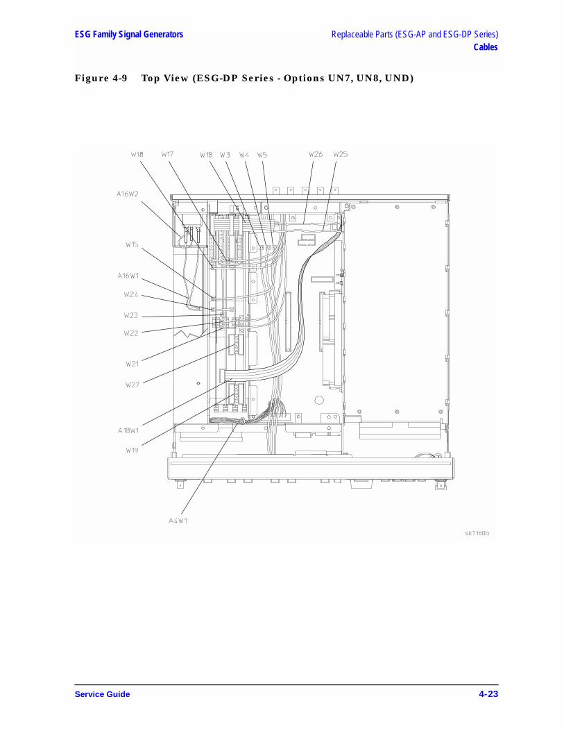
ESG Family Signal Generators Replaceable Parts (ESG-AP and ESG-DP Series)Cables
Figure 4-9 Top View (ESG-DP Series - Options UN7, UN8, UND)
Service Guide 4-23
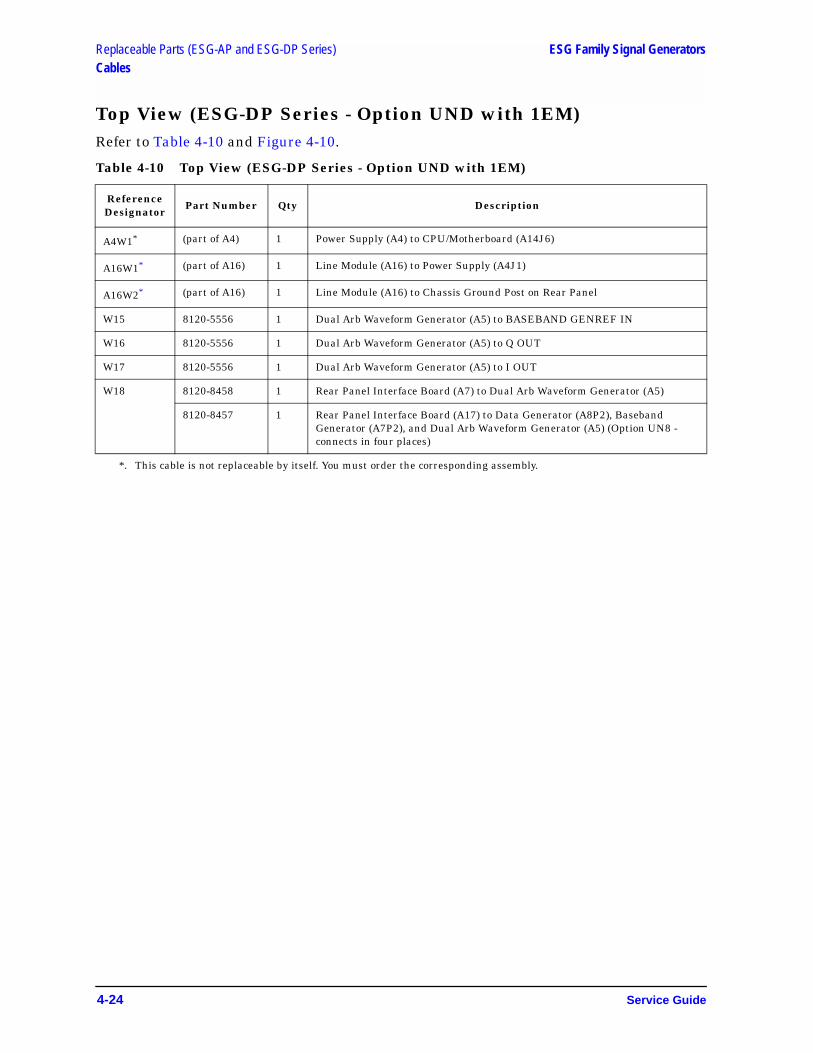
Replaceable Parts (ESG-AP and ESG-DP Series) ESG Family Signal GeneratorsCables
Top View (ESG-DP Series - Option UND with 1EM)Refer to Table 4-10 and Figure 4-10.
Table 4-10 Top View (ESG-DP Series - Option UND with 1EM)
Reference Designator
Part Number Qty Description
A4W1*
*. This cable is not replaceable by itself. You must order the corresponding assembly.
(part of A4) 1 Power Supply (A4) to CPU/Motherboard (A14J6)
A16W1* (part of A16) 1 Line Module (A16) to Power Supply (A4J1)
A16W2* (part of A16) 1 Line Module (A16) to Chassis Ground Post on Rear Panel
W15 8120-5556 1 Dual Arb Waveform Generator (A5) to BASEBAND GENREF IN
W16 8120-5556 1 Dual Arb Waveform Generator (A5) to Q OUT
W17 8120-5556 1 Dual Arb Waveform Generator (A5) to I OUT
W18 8120-8458 1 Rear Panel Interface Board (A7) to Dual Arb Waveform Generator (A5)
8120-8457 1 Rear Panel Interface Board (A17) to Data Generator (A8P2), Baseband Generator (A7P2), and Dual Arb Waveform Generator (A5) (Option UN8 - connects in four places)
4-24 Service Guide
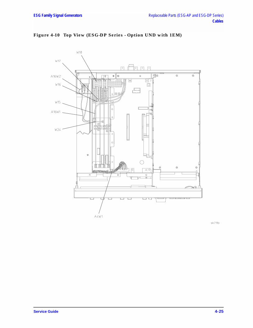
ESG Family Signal Generators Replaceable Parts (ESG-AP and ESG-DP Series)Cables
Figure 4-10 Top View (ESG-DP Series - Option UND with 1EM)
Service Guide 4-25
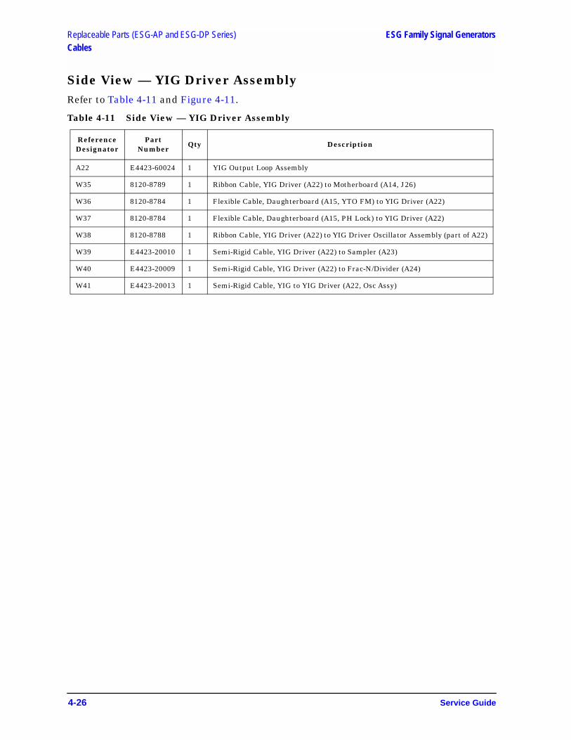
Replaceable Parts (ESG-AP and ESG-DP Series) ESG Family Signal GeneratorsCables
Side View — YIG Driver AssemblyRefer to Table 4-11 and Figure 4-11.
Table 4-11 Side View — YIG Driver Assembly
Reference Designator
Part Number
Qty Description
A22 E4423-60024 1 YIG Output Loop Assembly
W35 8120-8789 1 Ribbon Cable, YIG Driver (A22) to Motherboard (A14, J26)
W36 8120-8784 1 Flexible Cable, Daughterboard (A15, YTO FM) to YIG Driver (A22)
W37 8120-8784 1 Flexible Cable, Daughterboard (A15, PH Lock) to YIG Driver (A22)
W38 8120-8788 1 Ribbon Cable, YIG Driver (A22) to YIG Driver Oscillator Assembly (part of A22)
W39 E4423-20010 1 Semi-Rigid Cable, YIG Driver (A22) to Sampler (A23)
W40 E4423-20009 1 Semi-Rigid Cable, YIG Driver (A22) to Frac-N/Divider (A24)
W41 E4423-20013 1 Semi-Rigid Cable, YIG to YIG Driver (A22, Osc Assy)
4-26 Service Guide

ESG Family Signal Generators Replaceable Parts (ESG-AP and ESG-DP Series)Cables
Figure 4-11 Side View — YIG Driver Assembly
Service Guide 4-27

Replaceable Parts (ESG-AP and ESG-DP Series) ESG Family Signal GeneratorsCables
Inside Front Panel ViewRefer to Table 4-12 and Figure 4-12.
Table 4-12 Inside Front Panel View
NOTE The figure on the adjacent page represents an ESG-DP series front panel having option UN8. On a standard ESG-DP series front panel, W3, W4, and W5 do not exist and the front panel connectors for W1 and W2 will be in a slightly different location. An ESG-AP series front panel does not include W1 through W5, but will include W47 with Option 1E6 (not shown). All models having Option 1EM do not have W1 through W9 on the front panel.
Reference Designator
Part Number Qty Description
A1W1*
*. This cable is not replaceable by itself. You must order the corresponding assembly.
(part of A1) 1 Front Panel Board (A1) to CPU/Motherboard (A14J20)
A2DS1W1* (part of A2DS1) 1 Florescent Lamp (A2DS1) to A3W2
A3W1* (part of A3) 1 Inverter (A3) to CPU/Motherboard (A14J19)
A3W2* (part of A3) 1 Inverter (A3) to A2DS1W1
B1W1* (part of B1) 1 Small Fan (B1) to CPU/Motherboard (A14J16)
B2W1* (part of B2) 1 Large Fan (B2) to CPU/Motherboard (A14J17)
W1 8120-8786 1 I IN to Daughterboard (A15J2)
W2 8120-8786 1 Q IN to Daughterboard (A15J3)
W3 8120-5063 1 DATA to Baseband Generator (A7P100) (Options UN8)
W4 8120-5063 1 DATA CLOCK to Baseband Generator (A7P103) (Options UN8)
W5 8120-5063 1 SYMBOL SYNC to Baseband Generator (A7P101) (Options UN8)
W6 8120-8786 1 EXT 1 to Daughterboard (A15J4)
W7 8120-8786 1 EXT 2 to Daughterboard (A15J5)
W8 8120-8786 1 LF OUTPUT to Daughterboard (A15J6)
W9 E4400-20018 1 RF OUTPUT to Electronic Attenuator/RPP (AT1)
E4400-20125 1 RF OUTPUT to RPP (AT1) (Option 1EM, UNB)
W10 8120-6759 1 Display (A2) to CPU/Motherboard (A14J21)
W47 8120-8783 1 Flexible Cable, PULSE IN (FP) to Pulse Modulator (A25) (Option 1E6 - not shown)
4-28 Service Guide
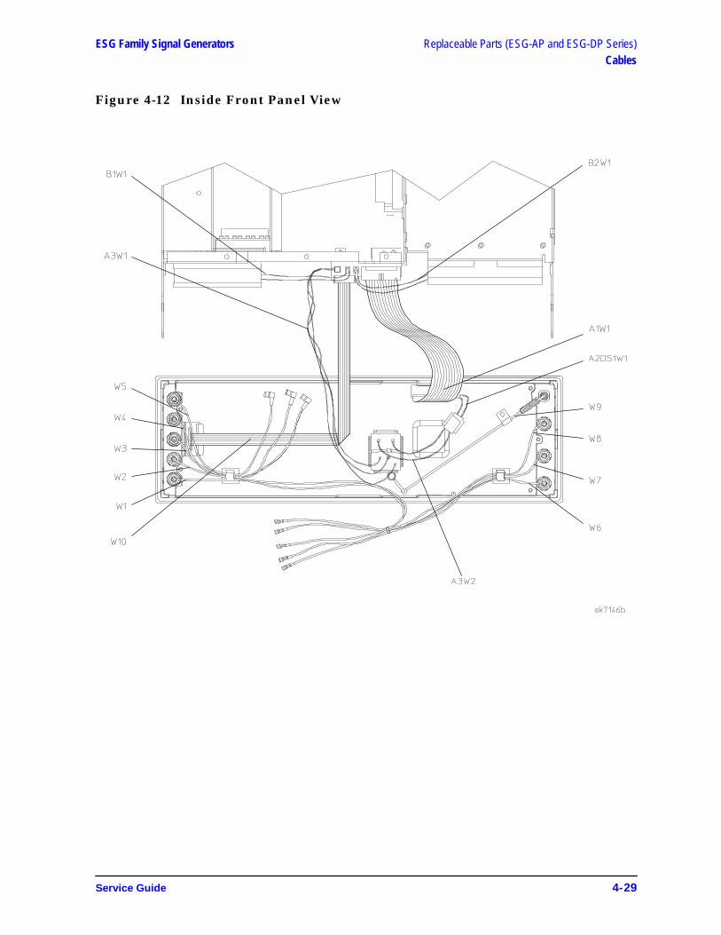
ESG Family Signal Generators Replaceable Parts (ESG-AP and ESG-DP Series)Cables
Figure 4-12 Inside Front Panel View
Service Guide 4-29
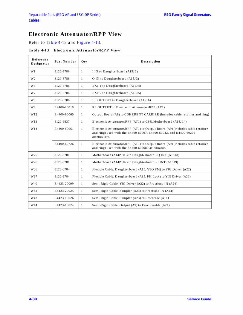
Replaceable Parts (ESG-AP and ESG-DP Series) ESG Family Signal GeneratorsCables
Electronic Attenuator/RPP ViewRefer to Table 4-13 and Figure 4-13.
Table 4-13 Electronic Attenuator/RPP View
Reference Designator
Part Number Qty Description
W1 8120-8786 1 I IN to Daughterboard (A15J2)
W2 8120-8786 1 Q IN to Daughterboard (A15J3)
W6 8120-8786 1 EXT 1 to Daughterboard (A15J4)
W7 8120-8786 1 EXT 2 to Daughterboard (A15J5)
W8 8120-8786 1 LF OUTPUT to Daughterboard (A15J6)
W9 E4400-20018 1 RF OUTPUT to Electronic Attenuator/RPP (AT1)
W12 E4400-60060 1 Output Board (A9) to COHERENT CARRIER (includes cable retainer and ring)
W13 8120-6837 1 Electronic Attenuator/RPP (AT1) to CPU/Motherboard (A14J14)
W14 E4400-60061 1 Electronic Attenuator/RPP (AT1) to Output Board (A9) (includes cable retainer and ring) used with the E4400-60007, E4400-60042, and E4400-60205 attenuators.
E4400-60726 1 Electronic Attenuator/RPP (AT1) to Output Board (A9) (includes cable retainer and ring) used with the E4400-600680 attenuator.
W25 8120-8781 1 Motherboard (A14P103) to Daughterboard - Q INT (A15J8)
W26 8120-8781 1 Motherboard (A14P102) to Daughterboard - I INT (A15J9)
W36 8120-8784 1 Flexible Cable, Daughterboard (A15, YTO FM) to YIG Driver (A22)
W37 8120-8784 1 Flexible Cable, Daughterboard (A15, PH Lock) to YIG Driver (A22)
W40 E4423-20009 1 Semi-Rigid Cable, YIG Driver (A22) to Fractional-N (A24)
W42 E4423-20025 1 Semi-Rigid Cable, Sampler (A23) to Fractional-N (A24)
W43 E4423-10026 1 Semi-Rigid Cable, Sampler (A23) to Reference (A11)
W44 E4423-10024 1 Semi-Rigid Cable, Output (A9) to Fractional-N (A24)
4-30 Service Guide
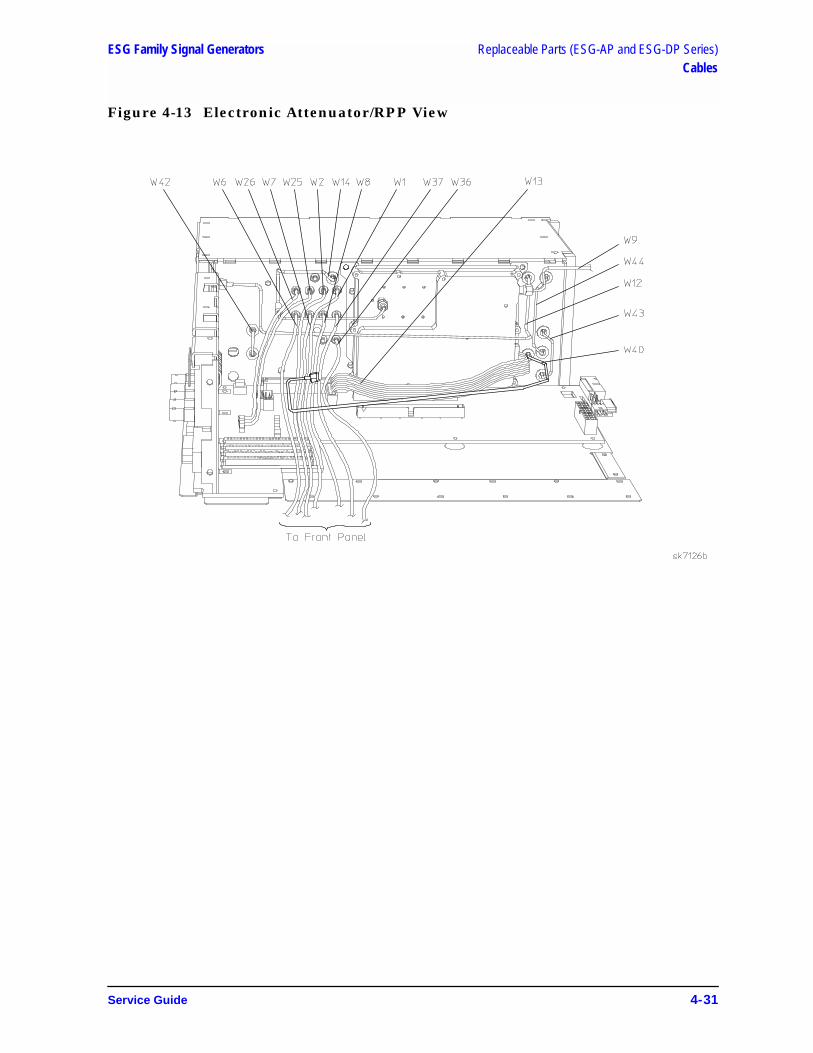
ESG Family Signal Generators Replaceable Parts (ESG-AP and ESG-DP Series)Cables
Figure 4-13 Electronic Attenuator/RPP View
Service Guide 4-31
Replaceable Parts (ESG-AP and ESG-DP Series) ESG Family Signal GeneratorsCables
Electronic Attenuator/RPP View (with Option 1EM)Refer to Table 4-14 and Figure 4-14.
Table 4-14 Electronic Attenuator/RPP View (with Option 1EM)
Reference Designator
Part Number Qty Description
W1 8120-8786 1 I IN to Daughterboard (A15J2)
W2 8120-8786 1 Q IN to Daughterboard (A15J3)
W6 8120-8786 1 EXT 1 to Daughterboard (A15J4)
W7 8120-8786 1 EXT 2 to Daughterboard (A15J5)
W8 8120-8786 1 LF OUTPUT to Daughterboard (A15J6)
W9 E4400-20025 1 RF OUTPUT to Electronic Attenuator/RPP (AT1)
W12 E4400-60060 1 Output Board (A9) to COHERENT CARRIER (includes cable retainer and ring)
W13 8120-6837 1 Electronic Attenuator/RPP (AT1) to CPU/Motherboard (A14J14)
W14 E4400-60061 1 Electronic Attenuator/RPP (AT1) to Output Board (A9) (includes cable retainer and ring) used with the E4400-60007, E4400-60042, and E4400-60680 attenuators.
E4400-60726 1 Electronic Attenuator/RPP (AT1) to Output Board (A9) (includes cable retainer and ring) used with the E4400-60680 attenuator.
W25 8120-8781 1 Motherboard (A14P103) to Daughterboard - Q INT (A15J8)
W26 8120-8781 1 Motherboard (A14P102) to Daughterboard - I INT (A15J9)
W36 8120-8784 1 Flexible Cable, Daughterboard (A15, YTO FM) to YIG Driver (A22)
W37 8120-8784 1 Flexible Cable, Daughterboard (A15, PH Lock) to YIG Driver (A22)
W40 E4423-20009 1 Semi-Rigid Cable, YIG Driver (A22) to Fractional-N (A24)
W42 E4423-20025 1 Semi-Rigid Cable, Sampler (A23) to Fractional-N (A24)
W43 E4423-10026 1 Semi-Rigid Cable, Sampler (A23) to Reference (A11)
W44 E4423-10024 1 Semi-Rigid Cable, Output (A9) to Fractional-N (A24)
4-32 Service Guide

ESG Family Signal Generators Replaceable Parts (ESG-AP and ESG-DP Series)Cables
Figure 4-14 Electronic Attenuator/RPP View (with Option 1EM)
Service Guide 4-33
Replaceable Parts (ESG-AP and ESG-DP Series) ESG Family Signal GeneratorsCables
Mechanical Attenuator View (Option UNB)Refer to Table 4-15 and Figure 4-15.
Table 4-15 Mechanical Attenuator View (Option UNB)
Reference Designator
Part Number Qty Description
A19W1*
*. This cable is not replaceable by itself. You must order the corresponding assembly.
(part of A19) 1 RPP (A19) to Motherboard (A14J15)
W1 8120-8786 1 I IN to Daughterboard (A15J2)
W2 8120-8786 1 Q IN to Daughterboard (A15J3)
W6 8120-8786 1 EXT 1 to Daughterboard (A15J4)
W7 8120-8786 1 EXT 2 to Daughterboard (A15J5)
W8 8120-8786 1 LF OUTPUT to Daughterboard (A15J6)
W9 E4400-20125 1 RF OUTPUT to RPP (A19)
W12 E4400-60060 1 Output Board (A9) to COHERENT CARRIER (includes cable retainer and ring)
W13 E4400-20132 1 Mechanical Attenuator (AT1) to CPU/Motherboard (A14J14)
W14 E4400-60177 1 Mechanical Attenuator (AT1) to Output Board (A9) (includes cable retainer and ring)
W20 E4400-20126 1 Semi-Rigid Cable, Mechanical Attenuator (AT1) to RPP (A19)
W25 8120-8781 1 Motherboard (A14P103) to Daughterboard - Q INT (A15J8)
W26 8120-8781 1 Motherboard (A14P102) to Daughterboard - I INT (A15J9)
W36 8120-8784 1 Flexible Cable, Daughterboard (A15, YTO FM) to YIG Driver (A22)
W37 8120-8784 1 Flexible Cable, Daughterboard (A15, PH Lock) to YIG Driver (A22)
W40 E4423-20009 1 Semi-Rigid Cable, YIG Driver (A22) to Fractional-N (A24)
W42 E4423-20025 1 Semi-Rigid Cable, Sampler (A23) to Fractional-N (A24)
W43 E4423-10026 1 Semi-Rigid Cable, Sampler (A23) to Reference (A11)
W44 E4423-10024 1 Semi-Rigid Cable, Output (A9) to Fractional-N (A24)
4-34 Service Guide

ESG Family Signal Generators Replaceable Parts (ESG-AP and ESG-DP Series)Cables
Figure 4-15 Mechanical Attenuator View (Option UNB)
Service Guide 4-35

Replaceable Parts (ESG-AP and ESG-DP Series) ESG Family Signal GeneratorsCables
Mechanical Attenuator View (Option UNB with 1EM)Refer to Table 4-16 and Figure 4-16.
Table 4-16 Mechanical Attenuator View (Option UNB with 1EM)
Reference Designator
Part Number Qty Description
A19W1*
*. This cable is not replaceable by itself. You must order the corresponding assembly.
(part of A19) 1 RPP (A19) to Motherboard (A14J15)
W1 8120-8786 1 I IN to Daughterboard (A15J2)
W2 8120-8786 1 Q IN to Daughterboard (A15J3)
W6 8120-8786 1 EXT 1 to Daughterboard (A15J4)
W7 8120-8786 1 EXT 2 to Daughterboard (A15J5)
W8 8120-8786 1 LF OUTPUT to Daughterboard (A15J6)
W9 E4423-20012 1 RF OUTPUT to RPP (A19)
W12 E4400-60060 1 Output Board (A9) to COHERENT CARRIER (includes cable retainer and ring)
W13 E4400-20132 1 Mechanical Attenuator (AT1) to CPU/Motherboard (A14J14)
W14 E4400-60177 1 Mechanical Attenuator (AT1) to Output Board (A9) (includes cable retainer and ring)
W20 E4400-20126 1 Semi-Rigid Cable, Mechanical Attenuator (AT1) to RPP (A19)
W25 8120-8781 1 Motherboard (A14P103) to Daughterboard - Q INT (A15J8)
W26 8120-8781 1 Motherboard (A14P102) to Daughterboard - I INT (A15J9)
W36 8120-8784 1 Flexible Cable, Daughterboard (A15, YTO FM) to YIG Driver (A22)
W37 8120-8784 1 Flexible Cable, Daughterboard (A15, PH Lock) to YIG Driver (A22)
W40 E4423-20009 1 Semi-Rigid Cable, YIG Driver (A22) to Fractional-N (A24)
W42 E4423-20025 1 Semi-Rigid Cable, Sampler (A23) to Fractional-N (A24)
W43 E4423-10026 1 Semi-Rigid Cable, Sampler (A23) to Reference (A11)
W44 E4423-10024 1 Semi-Rigid Cable, Output (A9) to Fractional-N (A24)
4-36 Service Guide

ESG Family Signal Generators Replaceable Parts (ESG-AP and ESG-DP Series)Cables
Figure 4-16 Mechanical Attenuator View (Option UNB with 1EM)
Service Guide 4-37

Replaceable Parts (ESG-AP and ESG-DP Series) ESG Family Signal GeneratorsCables
Pulse Modulator View (Option 1E6)Refer to Table 4-17 and Figure 4-17.
Table 4-17 Pulse Modulator View (Option 1E6)
Figure 4-17 Pulse Modulator View (Option 1E6)
Reference Designator
Part Number Qty Description
A25W1 (part of A25) 1 Wire Harness, Pulse Modulator (A25) to Motherboard (A14)
W45 E4423-20017 1 Semi-Rigid Cable, Output (A9) to Pulse Modulator (A25)
E4423-20012 1 Semi-Rigid Cable, Output (A9) to Pulse Modulator (A25)(Option UNB - not shown)
W46 E4423-20014 1 Semi-Rigid Cable, Electronic Attenuator (AT1) to Pulse Modulator (A25) used with the E4400-60007, E4400-60042, and E4400-60205 attenuators.
E4423-20726 1 Semi-Rigid Cable, Electronic Attenuator (AT1) to Pulse Modulator (A25) used with the E4400-60680 attenuator.
E4423-20011 Semi-Rigid Cable, Mechanical Attenuator (AT1) to Pulse Modulator (A25) (Option UNB - not shown)
W47 8120-8783 1 Flexible Cable, PULSE IN (FP) to Pulse Modulator (A25)
8120-8787 1 Flexible Cable, PULSE IN (RP) to Pulse Modulator (A25) (Option 1EM)
4-38 Service Guide

ESG Family Signal Generators Replaceable Parts (ESG-AP and ESG-DP Series)Hardware and Other Instrument Parts
Hardware and Other Instrument PartsThis section lists part numbers for hardware and other parts in your signal generator. Thefollowing instrument views are provided to help you locate specific parts.
• “Top View” on page 4-40
• “YIG Driver View” on page 4-42
• “Disassembled Mechanical Attenuator View (Option UNB)” on page 4-43
• “Disassembled Pulse Modulator View (Option 1E6)” on page 4-44
• “Disassembled Pulse Modulator View (Option 1E6/UNB)” on page 4-45
• “Front Panel View (ESG-AP Series)” on page 4-46
• “Front Panel View (ESG-DP Series)” on page 4-48
• “Disassembled Front-Panel View” on page 4-50
• “Daughterboard Card Cage View” on page 4-52
• “Inside Rear-Panel View” on page 4-53
• “Rear-Panel View (ESG-AP Series)” on page 4-54
• “Rear-Panel View (ESG-AP Series - Option 1EM)” on page 4-56
• “Rear-Panel View (ESG-DP Series)” on page 4-58
• “Rear Panel View (ESG-DP Series - Option 1EM)” on page 4-60
• “Instrument Chassis with Top and Right-Side Hardware” on page 4-62
• “Power Supply Shield and Left-Side Hardware” on page 4-64
• “Motherboard and Bottom-Side Hardware” on page 4-65
• “Instrument Cover and Associated Parts” on page 4-66
Service Guide 4-39
Replaceable Parts (ESG-AP and ESG-DP Series) ESG Family Signal GeneratorsHardware and Other Instrument Parts
Top ViewRefer to Table 4-18 and Figure 4-18.
Table 4-18 Top View
Item No. Part Number Qty Description
1 1400-0054 1 Clamp-Semi-Rigid Cable (W14)
2 0515-0372 1 Screw-Machine M3x8 CW-PN-TX
3 0515-0430 2 Screw-Machine M3x6 CW-PN-TX
4 0361-1341 4 Rivet-Plastic
5 0515-0374 4 Screw-Machine M3x10 CW-PN-TX
6 E4400-20041 1 Shield Cap
7 0400-0001 1 Grommet Round .562ID
8 0515-1521 2 Screw-Machine M3x5 FL-TX
9 E4400-60221 1 A14Q501 Transistor Assembly
10 0515-0374 1 Screw-Machine M3x10 CW-PN-TX
11 0340-1162 1 Bushing, Insulator 0.119 ID
12 0340-0614 1 Insulator Pad, Transistor TO-220
4-40 Service Guide
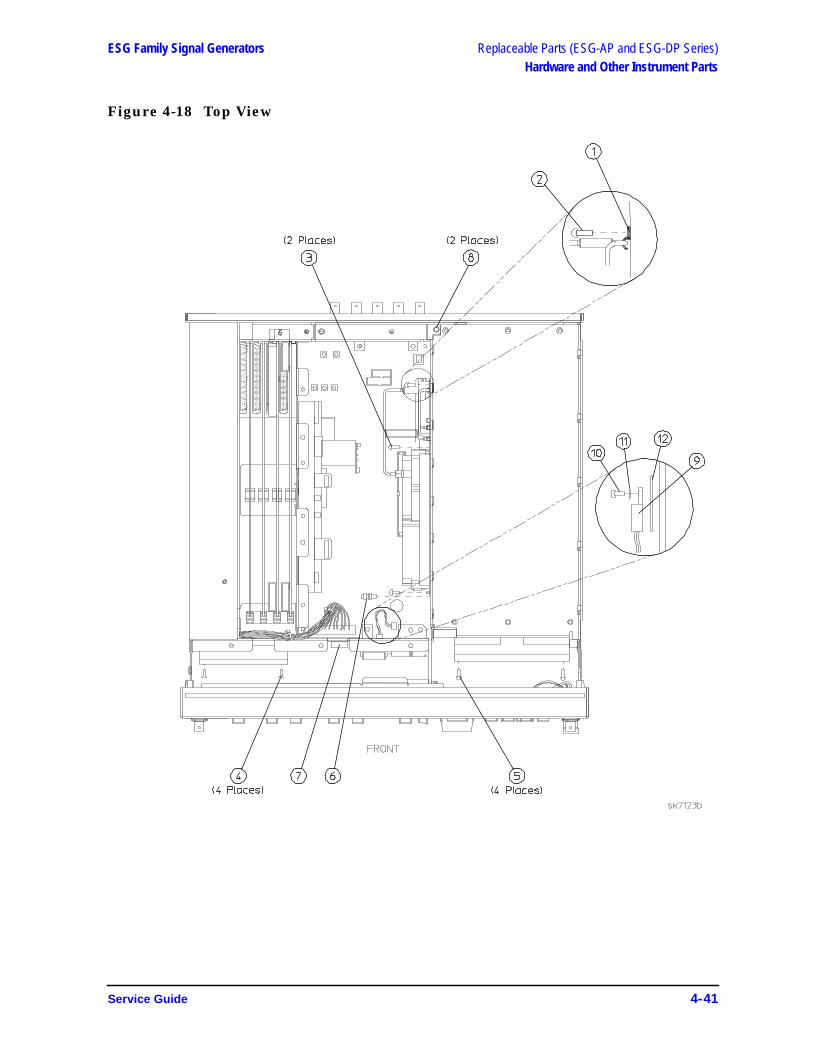
ESG Family Signal Generators Replaceable Parts (ESG-AP and ESG-DP Series)Hardware and Other Instrument Parts
Figure 4-18 Top View
Service Guide 4-41
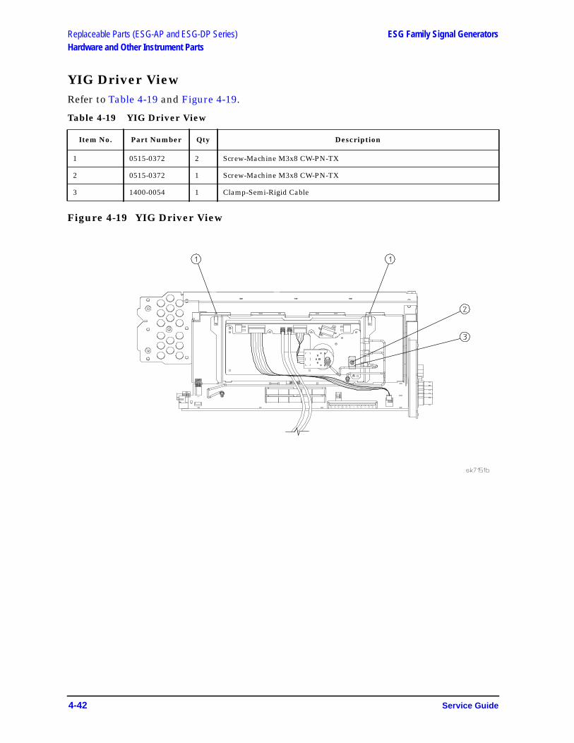
Replaceable Parts (ESG-AP and ESG-DP Series) ESG Family Signal GeneratorsHardware and Other Instrument Parts
YIG Driver ViewRefer to Table 4-19 and Figure 4-19.
Table 4-19 YIG Driver View
Figure 4-19 YIG Driver View
Item No. Part Number Qty Description
1 0515-0372 2 Screw-Machine M3x8 CW-PN-TX
2 0515-0372 1 Screw-Machine M3x8 CW-PN-TX
3 1400-0054 1 Clamp-Semi-Rigid Cable
4-42 Service Guide
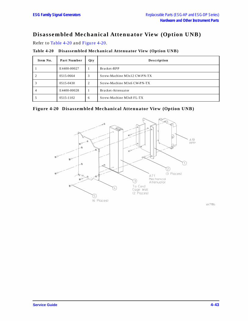
ESG Family Signal Generators Replaceable Parts (ESG-AP and ESG-DP Series)Hardware and Other Instrument Parts
Disassembled Mechanical Attenuator View (Option UNB)Refer to Table 4-20 and Figure 4-20.
Table 4-20 Disassembled Mechanical Attenuator View (Option UNB)
Figure 4-20 Disassembled Mechanical Attenuator View (Option UNB)
Item No. Part Number Qty Description
1 E4400-00027 1 Bracket-RPP
2 0515-0664 3 Screw-Machine M3x12 CW-PN-TX
3 0515-0430 2 Screw-Machine M3x6 CW-PN-TX
4 E4400-00028 1 Bracket-Attenuator
5 0515-1102 6 Screw-Machine M3x8 FL-TX
Service Guide 4-43

Replaceable Parts (ESG-AP and ESG-DP Series) ESG Family Signal GeneratorsHardware and Other Instrument Parts
Disassembled Pulse Modulator View (Option 1E6)Refer to Table 4-21 and Figure 4-21.
Table 4-21 Disassembled Pulse Modulator View (Option 1E6)
Figure 4-21 Disassembled Pulse Modulator View (Option 1E6)
Item No. Part Number Qty Description
1 0515-0372 2 Screw-Machine M3x8 CW-PN-TX
2 E4423-00003 1 Bracket-Pulse Modulator
3 0515-2001 2 Screw-Machine M2.5x10 FL-TX
4-44 Service Guide

ESG Family Signal Generators Replaceable Parts (ESG-AP and ESG-DP Series)Hardware and Other Instrument Parts
Disassembled Pulse Modulator View (Option 1E6/UNB)Refer to Table 4-22 and Figure 4-22.
Table 4-22 Disassembled Pulse Modulator View (Option 1E6/UNB)
Figure 4-22 Disassembled Pulse Modulator View (Option 1E6/UNB)
Item No. Part Number Qty Description
1 E4400-00027 1 Bracket-RPP
2 0515-0664 3 Screw-Machine M3x12 CW-PN-TX
3 0515-0430 2 Screw-Machine M3x6 CW-PN-TX
4 E4400-00028 1 Bracket-Attenuator
5 0515-1102 6 Screw-Machine M3x8 FL-TX
6 0515-0367 2 Screw-Machine M2.5x8 CW-PN-TX
Service Guide 4-45

Replaceable Parts (ESG-AP and ESG-DP Series) ESG Family Signal GeneratorsHardware and Other Instrument Parts
Front Panel View (ESG-AP Series)Refer to Table 4-23 and Figure 4-23.
Table 4-23 Front Panel View (ESG-AP Series)
Item No. Part Number Qty Description
1 E4400-80011 1 Label-Connectors
2 E4423-80003 1 Nameplate - E4423B 250k - 1GHz
2 E4423-80004 1 Nameplate - E4424B 250k - 2GHz
2 E4423-80005 1 Nameplate - E4425B 250k - 3GHz
2 E4423-80006 1 Nameplate - E4426B 250k - 4GHz
3 E4400-40003 1 Knob-RPG
4 E4400-80016 1 Label-Keypad
5 2950-0035 3 Nut-Hex 15/32-32
6 3050-1919 3 Washer-Wavy.490ID
7 E4400-80017 1 Label-Keypad (Option 1EM)
8 E4423-80001 1 Label-Connectors (Option 1E6)
9 2950-0035 4 Nut-Hex 15/32-32
10 3050-1919 4 Washer-Wavy.490ID
4-46 Service Guide

ESG Family Signal Generators Replaceable Parts (ESG-AP and ESG-DP Series) Hardware and Other Instrument Parts
Figure 4-23 Front Panel View (ESG-AP Series)
Service Guide 4-47
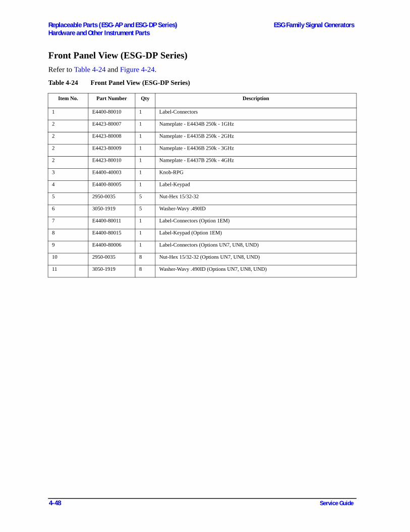
Replaceable Parts (ESG-AP and ESG-DP Series) ESG Family Signal GeneratorsHardware and Other Instrument Parts
Front Panel View (ESG-DP Series)Refer to Table 4-24 and Figure 4-24.
Table 4-24 Front Panel View (ESG-DP Series)
Item No. Part Number Qty Description
1 E4400-80010 1 Label-Connectors
2 E4423-80007 1 Nameplate - E4434B 250k - 1GHz
2 E4423-80008 1 Nameplate - E4435B 250k - 2GHz
2 E4423-80009 1 Nameplate - E4436B 250k - 3GHz
2 E4423-80010 1 Nameplate - E4437B 250k - 4GHz
3 E4400-40003 1 Knob-RPG
4 E4400-80005 1 Label-Keypad
5 2950-0035 5 Nut-Hex 15/32-32
6 3050-1919 5 Washer-Wavy .490ID
7 E4400-80011 1 Label-Connectors (Option 1EM)
8 E4400-80015 1 Label-Keypad (Option 1EM)
9 E4400-80006 1 Label-Connectors (Options UN7, UN8, UND)
10 2950-0035 8 Nut-Hex 15/32-32 (Options UN7, UN8, UND)
11 3050-1919 8 Washer-Wavy .490ID (Options UN7, UN8, UND)
4-48 Service Guide

ESG Family Signal Generators Replaceable Parts (ESG-AP and ESG-DP Series)Hardware and Other Instrument Parts
Figure 4-24 Front-Panel View (ESG-DP Series)
Service Guide 4-49

Replaceable Parts (ESG-AP and ESG-DP Series) ESG Family Signal GeneratorsHardware and Other Instrument Parts
Disassembled Front-Panel ViewRefer to Table 4-25 and Figure 4-25.
Table 4-25 Disassembled Front-Panel View
Item No. Part Number Qty Description
1 1250-1811 1 Adapter-Female SMA to Female Type-N
2 E4400-20012 1 Frame-Front
3 3050-1935 1 Washer-Flat
4 2190-0383 1 Washer-Lock
5 2950-0054 1 Nut-Hex 1/2-28
6 E4400-40001 1 Rubber Keypad
7 0515-1521 5 Screw-Machine M3x5 FL-TX
8 0515-0372 4 Screw-Machine M3x8 CW-PN-TX
9 1400-1594 2*
*. ESG-AP Series uses a quantity of one.
Clamp-Flexible Cables
10 0515-0372 8 Screw-Machine M3x8 CW-PN-TX
11 1400-0054 1 Clamp-Semi-Rigid Cable (W9)
12 1400-1533 1 Clamp-Ribbon Cable (A1W1)
13 1400-0493 1 Cable Tie Wrap
14 1400-0611 1 Clamp-Ribbon Cable (W10)
15 E4400-00008 1 Front Frame RFI Shield
16 E4400-00009 1 Filter Bracket
17 4330-1711 1 Glass Filter 70% XMT
18 E4400-40008 1 Light Pipe
19 8160-0723 2 Ft Spiral Gasket-BC CY .094
20 8160-0660 4 Ft RFI Round Mesh.125
21 0515-1227 9 Screw-Machine M3x6 FL-TX
4-50 Service Guide

ESG Family Signal Generators Replaceable Parts (ESG-AP and ESG-DP Series)Hardware and Other Instrument Parts
Figure 4-25 Disassembled Front-Panel View
Service Guide 4-51

Replaceable Parts (ESG-AP and ESG-DP Series) ESG Family Signal GeneratorsHardware and Other Instrument Parts
Daughterboard Card Cage ViewRefer to Table 4-26 and Figure 4-26.
Table 4-26 Daughterboard Card Cage View
Figure 4-26 Daughterboard Card Cage View
Item No. Part Number Qty Description
1 E4400-40002 10 Retainer-Cable
2 0510-1643 10 Retainer Ring .309ID
3 0515-0430 5 Screw-Machine M3x6 CW-PN-TX
4-52 Service Guide

ESG Family Signal Generators Replaceable Parts (ESG-AP and ESG-DP Series)Hardware and Other Instrument Parts
Inside Rear-Panel ViewRefer to Table 4-27 and Figure 4-27.
Table 4-27 Inside Rear-Panel View
Figure 4-27 Inside Rear-Panel View
Item No. Part Number Qty Description
1 0535-0031 2 Nut-Hex M3.0
Service Guide 4-53
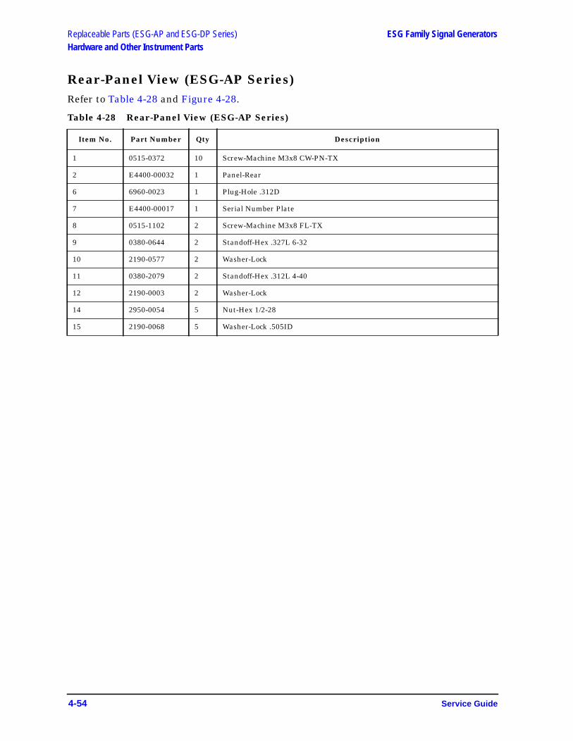
Replaceable Parts (ESG-AP and ESG-DP Series) ESG Family Signal GeneratorsHardware and Other Instrument Parts
Rear-Panel View (ESG-AP Series)Refer to Table 4-28 and Figure 4-28.
Table 4-28 Rear-Panel View (ESG-AP Series)
Item No. Part Number Qty Description
1 0515-0372 10 Screw-Machine M3x8 CW-PN-TX
2 E4400-00032 1 Panel-Rear
6 6960-0023 1 Plug-Hole .312D
7 E4400-00017 1 Serial Number Plate
8 0515-1102 2 Screw-Machine M3x8 FL-TX
9 0380-0644 2 Standoff-Hex .327L 6-32
10 2190-0577 2 Washer-Lock
11 0380-2079 2 Standoff-Hex .312L 4-40
12 2190-0003 2 Washer-Lock
14 2950-0054 5 Nut-Hex 1/2-28
15 2190-0068 5 Washer-Lock .505ID
4-54 Service Guide

ESG Family Signal Generators Replaceable Parts (ESG-AP and ESG-DP Series)Hardware and Other Instrument Parts
Figure 4-28 Rear-Panel View (ESG-AP Series)
Service Guide 4-55
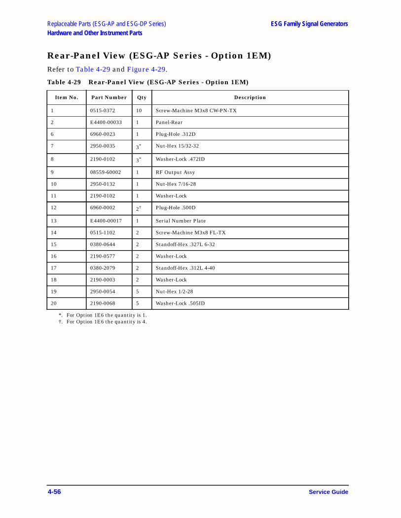
Replaceable Parts (ESG-AP and ESG-DP Series) ESG Family Signal GeneratorsHardware and Other Instrument Parts
Rear-Panel View (ESG-AP Series - Option 1EM)Refer to Table 4-29 and Figure 4-29.
Table 4-29 Rear-Panel View (ESG-AP Series - Option 1EM)
Item No. Part Number Qty Description
1 0515-0372 10 Screw-Machine M3x8 CW-PN-TX
2 E4400-00033 1 Panel-Rear
6 6960-0023 1 Plug-Hole .312D
7 2950-0035 3*
*. For Option 1E6 the quantity is 1.
Nut-Hex 15/32-32
8 2190-0102 3* Washer-Lock .472ID
9 08559-60002 1 RF Output Assy
10 2950-0132 1 Nut-Hex 7/16-28
11 2190-0102 1 Washer-Lock
12 6960-0002 2†
†. For Option 1E6 the quantity is 4.
Plug-Hole .500D
13 E4400-00017 1 Serial Number Plate
14 0515-1102 2 Screw-Machine M3x8 FL-TX
15 0380-0644 2 Standoff-Hex .327L 6-32
16 2190-0577 2 Washer-Lock
17 0380-2079 2 Standoff-Hex .312L 4-40
18 2190-0003 2 Washer-Lock
19 2950-0054 5 Nut-Hex 1/2-28
20 2190-0068 5 Washer-Lock .505ID
4-56 Service Guide
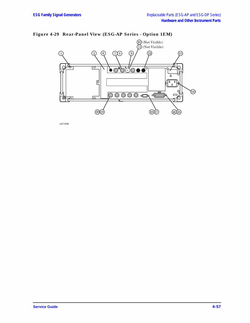
ESG Family Signal Generators Replaceable Parts (ESG-AP and ESG-DP Series)Hardware and Other Instrument Parts
Figure 4-29 Rear-Panel View (ESG-AP Series - Option 1EM)
Service Guide 4-57

Replaceable Parts (ESG-AP and ESG-DP Series) ESG Family Signal GeneratorsHardware and Other Instrument Parts
Rear-Panel View (ESG-DP Series)Refer to Table 4-30 and Figure 4-30.
Table 4-30 Rear-Panel View (ESG-DP Series)
Item No. Part Number Qty Description
1 0515-0372 10 Screw-Machine M3x8 CW-PN-TX
2 E4400-00032 1 Panel-Rear
3 0515-0372 1 Screw-Machine M3x8 CW-PN-TX (used to attach item 4))
4 1250-2759 1 Dust Cap Female SMA
5 1250-1753 1 Adapter-Female SMA to Female SMA
7 E4400-00017 1 Serial Number Plate
8 0515-1102 2 Screw-Machine M3x8 FL-TX
9 0380-0644 2 Standoff-Hex .327L 6-32
10 2190-0577 2 Washer-Lock
11 0380-2079 2 Standoff-Hex .312L 4-40
12 2190-0003 2 Washer-Lock
13 6960-0002 3 Plug-Hole .500D (Options UN8, UND)
14 2950-0054 5 Nut-Hex 1/2-28
15 2190-0068 5 Washer-Lock .505ID
16 2950-0035 11 Nut-Hex 15/32-32 (Options UN8, UND)
17 2190-0102 11 Washer-Lock .472ID (Options UN8, UND)
18 E4400-00031 1 Panel-Rear (Options UN8, UND)
19 2950-0035 14 Nut-Hex 15/32-32 (Option UN7)
20 2190-0102 14 Washer-Lock .472ID (Option UN7)
21 E4400-00025 1 Panel-Rear (Option UN7)
22 2950-0078 5 Nut-Hex 10-32 (for the SMBs) (Option UN7)
23 2190-0124 5 Washer-Lock .195ID (for the SMBs) (Option UN7)
4-58 Service Guide

ESG Family Signal Generators Replaceable Parts (ESG-AP and ESG-DP Series)Hardware and Other Instrument Parts
Figure 4-30 Rear-Panel View (ESG-DP Series)
Service Guide 4-59

Replaceable Parts (ESG-AP and ESG-DP Series) ESG Family Signal GeneratorsHardware and Other Instrument Parts
Rear Panel View (ESG-DP Series - Option 1EM)Refer to Table 4-31 and Figure 4-31.
Table 4-31 Rear Panel View (ESG-DP Series - Option 1EM)
Item No. Part Number Qty Description
1 0515-0372 10 Screw-Machine M3x8 CW-PN-TX
2 E4400-00033 1 Panel-Rear
3 0515-0372 1 Screw-Machine M3x8 CW-PN-TX (used to attach item 4)
4 1250-2759 1 Dust Cap Female SMA
5 1250-1753 1 Adapter-Female SMA to Female SMA
7 2950-0035 5 Nut-Hex 15/32-32
8 2190-0102 5 Washer-Lock .472ID
9 08559-60002 1 RF Output Assy
10 2950-0132 1 Nut-Hex 7/16-28
11 2190-0102 1 Washer-Lock
13 E4400-00017 1 Serial Number Plate
14 0515-1102 2 Screw-Machine M3x8 FL-TX
15 0380-0644 2 Standoff-Hex .327L 6-32
16 2190-0577 2 Washer-Lock
17 0380-2079 2 Standoff-Hex .312L 4-40
18 2190-0003 2 Washer-Lock
19 2950-0054 5 Nut-Hex 1/2-28
20 2190-0068 5 Washer-Lock .505ID
21 E4400-00034 1 Panel-Rear (Option UN8)
22 2950-0078 14 Nut-Hex 10-32 (for the SMBs) (Options UN8, UND)
23 2190-0124 14 Washer-Lock .195ID (for the SMBs) (Options UN8, UND)
24 E4400-00026 1 Panel-Rear (Option UN7)
25 2950-0078 22 Nut-Hex 10-32 (for the SMBs) (Option UN7)
26 2190-0124 22 Washer-Lock .195ID (for the SMBs) (Option UN7)
4-60 Service Guide

ESG Family Signal Generators Replaceable Parts (ESG-AP and ESG-DP Series)Hardware and Other Instrument Parts
Figure 4-31 Rear-Panel View (ESG-DP Series - Option 1EM)
Service Guide 4-61

Replaceable Parts (ESG-AP and ESG-DP Series) ESG Family Signal GeneratorsHardware and Other Instrument Parts
Instrument Chassis with Top and Right-Side HardwareRefer to Table 4-32 and Figure 4-32.
Table 4-32 Instrument Chassis with Top and Right-Side Hardware
Item No. Part Number Qty Description
1 0515-1269 2 Screw-Machine M4X10 FL-TX
2 0515-2087 4 Screw-Machine M3x6 CW-BN-TX
3 E4400-00003 1 Cover-Side (Serial Prefix US3833, or GB3832, and below)
3 E4400-00037 1 Cover-Side (Serial Prefix US3844, or GB3845, and above)
4 E4400-00035 1 Chassis
5 E4400-00036 1 Cover-Top Chassis
6 0515-0430 11 Screw-Machine M3x6 CW-PN-TX
7 E4423-80002 1 Label-Connection Diagram
4-62 Service Guide

ESG Family Signal Generators Replaceable Parts (ESG-AP and ESG-DP Series)Hardware and Other Instrument Parts
Figure 4-32 Instrument Chassis with Top and Right-Side Hardware
Service Guide 4-63
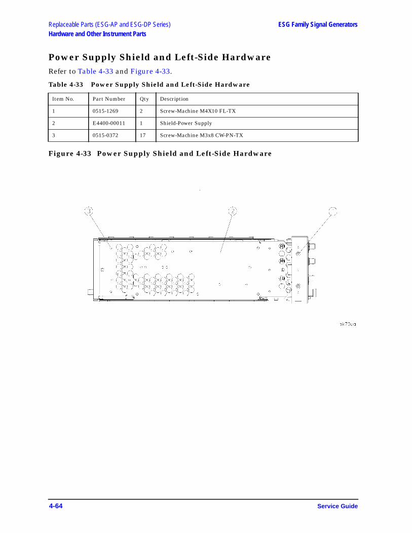
Replaceable Parts (ESG-AP and ESG-DP Series) ESG Family Signal GeneratorsHardware and Other Instrument Parts
Power Supply Shield and Left-Side HardwareRefer to Table 4-33 and Figure 4-33.
Table 4-33 Power Supply Shield and Left-Side Hardware
Figure 4-33 Power Supply Shield and Left-Side Hardware
Item No. Part Number Qty Description
1 0515-1269 2 Screw-Machine M4X10 FL-TX
2 E4400-00011 1 Shield-Power Supply
3 0515-0372 17 Screw-Machine M3x8 CW-PN-TX
4-64 Service Guide

ESG Family Signal Generators Replaceable Parts (ESG-AP and ESG-DP Series)Hardware and Other Instrument Parts
Motherboard and Bottom-Side HardwareRefer to Table 4-34 and Figure 4-34.
Table 4-34 Motherboard and Bottom-Side Hardware
Figure 4-34 Motherboard and Bottom-Side Hardware
Item No. Part Number Qty Description
1 0515-0372 15 Screw-Machine M3x8 CW-PN-TX
2 E4400-00007 1 Cover-Bottom Chassis
3 0515-0372 2 Screw-Machine M3x8 CW-PN-TX
Service Guide 4-65

Replaceable Parts (ESG-AP and ESG-DP Series) ESG Family Signal GeneratorsHardware and Other Instrument Parts
Instrument Cover and Associated PartsRefer to Table 4-35 and Figure 4-35.
Table 4-35 Instrument Cover and Associated Parts
Item No. Part Number Qty Description
1 0515-1619 4 Screw-Machine M4x25 PN-TX
2 5041-9611 4 Foot-Rear Long
3 5041-9167 4 Feet-Bottom
4 1460-1345 2 Spring-Wire Frame 3.000 Long
5 5041-9171 2 Side Trim
6 E4400-60026 2 Assy-Strap Handle - includes the following parts:
Item 6includesthese parts:
5063-9209 1 Strap Assembly
E4400-00015 2 Ground Spring
E4400-20023 2 Handle Retainer
E4400-40007 2 End Cap
0515-0710 2 Screw-Machine M5x18 FL-TX
7 E4400-00004 1 Cover-Instrument
4-66 Service Guide

ESG Family Signal Generators Replaceable Parts (ESG-AP and ESG-DP Series)Hardware and Other Instrument Parts
Figure 4-35 Instrument Cover and Associated Parts
Service Guide 4-67
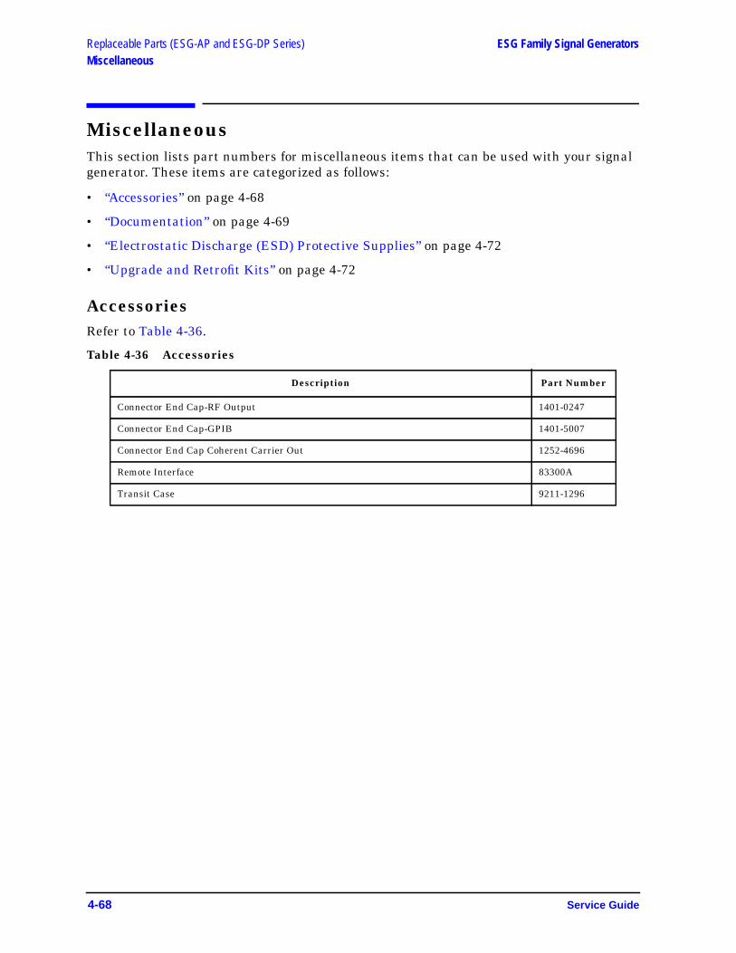
Replaceable Parts (ESG-AP and ESG-DP Series) ESG Family Signal GeneratorsMiscellaneous
MiscellaneousThis section lists part numbers for miscellaneous items that can be used with your signalgenerator. These items are categorized as follows:
• “Accessories” on page 4-68
• “Documentation” on page 4-69
• “Electrostatic Discharge (ESD) Protective Supplies” on page 4-72
• “Upgrade and Retrofit Kits” on page 4-72
AccessoriesRefer to Table 4-36.
Table 4-36 Accessories
Description Part Number
Connector End Cap-RF Output 1401-0247
Connector End Cap-GPIB 1401-5007
Connector End Cap Coherent Carrier Out 1252-4696
Remote Interface 83300A
Transit Case 9211-1296
4-68 Service Guide

ESG Family Signal Generators Replaceable Parts (ESG-AP and ESG-DP Series)Miscellaneous
DocumentationRefer to Table 4-37 and Table 4-38.
Table 4-37 ESG Family Signal Generators Documentation
Description Part Number
ESG-A and ESG-AP Series Manual Set (includes items listed below) E4400-90334
User’s Guide E4400-90323
Programming Guide E4400-90324
Calibration Guide E4400-90325
Quick Start Guide E4400-90326
Error Messages E4400-90333
Technical Specifications 5965-3096E
Feature Releases Document E4400-90363
ESG-D and ESG-DP Series Manual Set (includes items listed below) E4400-90322
User’s Guide E4400-90323
Programming Guide E4400-90324
Calibration Guide E4400-90325
Quick Start Guide E4400-90326
Error Messages E4400-90333
Technical Specifications 5965-3096E
Feature Releases Document E4400-90363
Option 200 Fully Coded 3GPP W-CDMA Personality User’s and Programming Guide E4400-90390
Option 201 Real-Time cdma2000 Personality User’s and Programming Guide E4400-90386
Option UN8 Real-Time I/Q Baseband Generator with TDMA Standards User’s andProgramming Guide (includes Option 202, EDGE)
E4400-90327
Option UND Dual Arbitrary Waveform Generator and Option UN5 Multichannel,Multicarrier CDMA Personality User’s and Programming Guide
E4400-90328
Option 100 W-CDMA Personality User’s and Programming Guide E4400-90329
Option 101 CDMA2000 Personality User’s and Programming Guide E4400-90330
Option UN7 Bit Error Rate Test User’s and Programming Guide E4400-90331
Option 300 Base Station BERT Extension for Option UN7 User’s and ProgrammingGuide
E4400-90305
Service Guide E4400-90335
Component-Level Information E4400-90336
Service Guide 4-69

Replaceable Parts (ESG-AP and ESG-DP Series) ESG Family Signal GeneratorsMiscellaneous
Table 4-38 Localized Documentation for ESG Family Signal Generators
Description Part Number
Chinese
User’s Guide - Chinese E4400-90172
Option UN8 DECT User’s and Programming Guide - Chinese E4400-90194
Option UN8 GSM User’s and Programming Guide - Chinese E4400-90201
Option UN8 Custom Digital Modulation User’s and Programming Guide - Chinese E4400-90180
Option UND Dual Arbitrary Waveform Generator and Option UN5 Multichannel,Multicarrier CDMA Personality User’s and Programming Guide - Chinese
E4400-90187
Taiwanese
User’s Guide - Taiwanese E4400-90173
Option UN8 DECT User’s and Programming Guide - Taiwanese E4400-90195
Option UN8 GSM User’s and Programming Guide - Taiwanese E4400-90202
Option UN8 Custom Digital Modulation User’s and Programming Guide - Taiwanese E4400-90181
Option UND Dual Arbitrary Waveform Generator and Option UN5 Multichannel,Multicarrier CDMA Personality User’s and Programming Guide - Taiwanese
E4400-90188
French
User’s Guide - French E4400-90174
Option UN8 DECT User’s and Programming Guide - French E4400-90196
Option UN8 GSM User’s and Programming Guide - French E4400-90203
Option UN8 TETRA User’s and Programming Guide - French E4400-90212
Option UN8 Custom Digital Modulation User’s and Programming Guide - French E4400-90182
Option UND Dual Arbitrary Waveform Generator and Option UN5 Multichannel,Multicarrier CDMA Personality User’s and Programming Guide - French
E4400-90189
German
User’s Guide - German E4400-90175
Option UN8 DECT User’s and Programming Guide - German E4400-90197
Option UN8 GSM User’s and Programming Guide - German E4400-90204
Option UN8 TETRA User’s and Programming Guide - German E4400-90210
Option UN8 Custom Digital Modulation User’s and Programming Guide - German E4400-90183
Option UND Dual Arbitrary Waveform Generator and Option UN5 Multichannel,Multicarrier CDMA Personality User’s and Programming Guide - German
E4400-90190
4-70 Service Guide

ESG Family Signal Generators Replaceable Parts (ESG-AP and ESG-DP Series)Miscellaneous
Japanese
User’s Guide - Japanese E4400-90176
Option UN8 DECT User’s and Programming Guide - Japanese E4400-90198
Option UN8 GSM User’s and Programming Guide - Japanese E4400-90205
Option UN8 PDC User’s and Programming Guide - Japanese E4400-90208
Option UN8 PHS User’s and Programming Guide - Japanese E4400-90209
Option UN8 Custom Digital Modulation User’s and Programming Guide - Japanese E4400-90184
Option UND Dual Arbitrary Waveform Generator and Option UN5 Multichannel,Multicarrier CDMA Personality User’s and Programming Guide - Japanese
E4400-90191
Option UN7 Bit Error Rate Test User’s and Programming Guide - Japanese E4400-90179
Korean
User’s Guide - Korean E4400-90177
Option UND Dual Arbitrary Waveform Generator and Option UN5 Multichannel,Multicarrier CDMA Personality User’s and Programming Guide - Korean
E4400-90192
Spanish
User’s Guide - Spanish E4400-90178
Option UN8 DECT User’s and Programming Guide - Spanish E4400-90200
Option UN8 GSM User’s and Programming Guide - Spanish E4400-90207
Option UN8 TETRA User’s and Programming Guide - Spanish E4400-90211
Option UN8 Custom Digital Modulation User’s and Programming Guide - Spanish E4400-90186
Option UND Dual Arbitrary Waveform Generator and Option UN5 Multichannel,Multicarrier CDMA Personality User’s and Programming Guide - Spanish
E4400-90193
Description Part Number
Service Guide 4-71
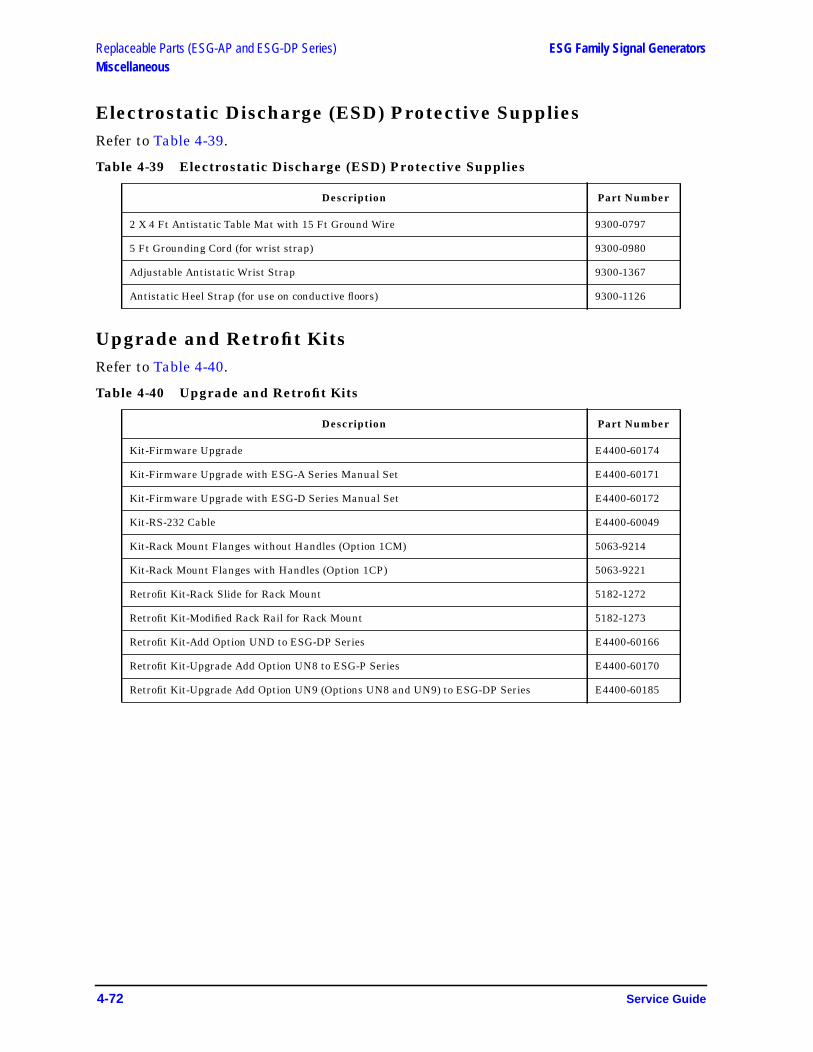
Replaceable Parts (ESG-AP and ESG-DP Series) ESG Family Signal GeneratorsMiscellaneous
Electrostatic Discharge (ESD) Protective SuppliesRefer to Table 4-39.
Table 4-39 Electrostatic Discharge (ESD) Protective Supplies
Upgrade and Retrofit KitsRefer to Table 4-40.
Table 4-40 Upgrade and Retrofit Kits
Description Part Number
2 X 4 Ft Antistatic Table Mat with 15 Ft Ground Wire 9300-0797
5 Ft Grounding Cord (for wrist strap) 9300-0980
Adjustable Antistatic Wrist Strap 9300-1367
Antistatic Heel Strap (for use on conductive floors) 9300-1126
Description Part Number
Kit-Firmware Upgrade E4400-60174
Kit-Firmware Upgrade with ESG-A Series Manual Set E4400-60171
Kit-Firmware Upgrade with ESG-D Series Manual Set E4400-60172
Kit-RS-232 Cable E4400-60049
Kit-Rack Mount Flanges without Handles (Option 1CM) 5063-9214
Kit-Rack Mount Flanges with Handles (Option 1CP) 5063-9221
Retrofit Kit-Rack Slide for Rack Mount 5182-1272
Retrofit Kit-Modified Rack Rail for Rack Mount 5182-1273
Retrofit Kit-Add Option UND to ESG-DP Series E4400-60166
Retrofit Kit-Upgrade Add Option UN8 to ESG-P Series E4400-60170
Retrofit Kit-Upgrade Add Option UN9 (Options UN8 and UN9) to ESG-DP Series E4400-60185
4-72 Service Guide
ESG Family Signal Generators
5 Assembly Replacement
This chapter provides removal and replacement procedures for the major assemblies ofyour signal generator.
Service Guide 5-1

Assembly Replacement ESG Family Signal GeneratorsBefore You Replace an Assembly
Before You Replace an AssemblyBe sure to review the warning and caution statements described in Chapter 7 prior toreplacing an assembly in your signal generator.
After Replacing an AssemblyAfter you have replaced or repaired an assembly, certain performance tests andadjustments may have to be performed. Chapter 6, “Post-Repair Procedures,” lists theperformance tests and adjustments required for each assembly.
5-2 Service Guide

ESG Family Signal Generators Assembly ReplacementAssemblies That You Can Replace
Assemblies That You Can ReplaceThis chapter provides removal and replacement procedures for the following assemblies:
• A1 Front Panel Board
• A2 Display
• A2DS1 Fluorescent Lamp
• A3 Inverter
• A4 Power Supply
• A4 Power Supply (with Option 1EM)
• A14 CPU/Motherboard
• A14BT1 Battery
• A14Q501 Transistor
• A15 Daughterboard
• A16 Line Module
• A17 and A18 Rear Panel Interface Boards
• A19 Reverse Power Protection (RPP)
• A20 Downconvertor
• A22 YIG Driver
• A25 Pulse Modulator
• A25 Pulse Modulator (with Option UNB)
• AT1 Electronic Attenuator/RPP
• AT1 Mechanical Attenuator
• B1 Small Fan
• B2 Large Fan
• Daughterboard Card Cage Boards
• Digital Card Cage Boards
• Front Panel
• Instrument Cover
• Rear Panel
• Rear Panel (with Option 1EM)
• Semi-Rigid Cables
Service Guide 5-3
Assembly Replacement ESG Family Signal GeneratorsA1 Front Panel Board
A1 Front Panel Board
Tools Required
• T-10 TORX screwdriver
• 5/16-inch open-end wrench
Removal
1. Remove the front panel assembly. (Refer to the “Front Panel” replacement procedure onpage 5-60.)
2. Remove the small bracket (item 1 in Figure 5-1) that secures W9 (not shown) to the RFIshield (item 2). Disconnect W9.
3. Remove the RFI shield by removing the seven screws (item 3) that secure it.
4. Remove the display (A2) by removing the four screws (item 4) that secure it.
5. Remove the front panel knob (item 5) by pulling it directly away from the front panel.
6. Remove the front panel board (A1) by removing the nine screws (item 6) that secure it.
Replacement
1. Reverse the removal procedure and do the following:
• Torque all T-10 TORX screws to 9 in-lbs.
• Torque W9 to 9 in-lbs.
5-4 Service Guide
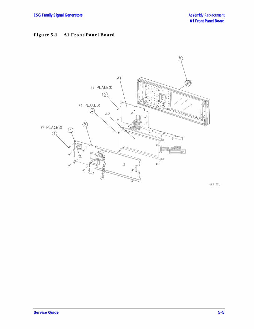
ESG Family Signal Generators Assembly ReplacementA1 Front Panel Board
Figure 5-1 A1 Front Panel Board
Service Guide 5-5
Assembly Replacement ESG Family Signal GeneratorsA2 Display
A2 Display
Tools Required
• T-10 TORX screwdriver
• 5/16-inch open-end wrench
Removal
1. Remove the front panel assembly. (Refer to the “Front Panel” replacement procedure onpage 5-60.)
2. Remove the small bracket (item 1 in Figure 5-2) that secures W9 (not shown) to the RFIshield (item 2). Disconnect W9.
3. Remove the RFI shield by removing the seven screws (item 3) that secure it.
4. Remove the display (A2) by removing the four screws (item 4) that secure it.
Replacement
1. Reverse the removal procedure and do the following:
• Torque all T-10 TORX screws to 9 in-lbs.
• Torque W9 to 9 in-lbs.
• If you know the part number of the replacement display, on the CPU/motherboard,set the jumpers for P104, P105, and P106 to the correct positions for your display.(See Figure 5-3.)
For part number 2090-0375, set P104, P105, and P106 to the + position.
For part number 1990-1910, set P104, P105, and P106 to the − position.
• If you do not know the part number of the replacement display, do the following:
a. On the CPU/motherboard, set the jumpers for P104, P105, and P106 to the+ position.
CAUTION Damage can occur to the CPU/motherboard if the signal generator remainsturned on for a prolonged period with the jumpers for P104, P105, and P106positioned incorrectly.
b. Turn the signal generator on, and observe the display.
c. If the display does not show text or characters within five seconds, turn the signalgenerator off and move the jumpers for P104, P105, and P106 to the − position.Repeat the previous step.
5-6 Service Guide

ESG Family Signal Generators Assembly ReplacementA2 Display
• On the A14 CPU/motherboard, set switch #4 on switch pack S201 to the correctposition for your display: (See Figure 5-3.)
If P104, P105, and P106 are set to the + position, set switch #4 of S201 to the up(open) position, away from the CPU/motherboard.
If P104, P105, and P106 are set to the − position, set switch #4 of S201 to the down(closed) position, toward the CPU/motherboard.
NOTE Switch #5 of S201 is set to the up (open) position in all circumstances.
NOTE You must reset the signal generator for the switch settings to take effect.
Figure 5-2 A2 Display (1 of 2)
Service Guide 5-7

Assembly Replacement ESG Family Signal GeneratorsA2 Display
Figure 5-3 A2 Display (2 of 2)
5-8 Service Guide

ESG Family Signal Generators Assembly ReplacementA2DS1 Fluorescent Lamp
A2DS1 Fluorescent Lamp
Tools Required
• Phillips #0 screwdriver
Removal
1. Remove the display (A2). (Refer to the “A2 Display” replacement procedure on page 5-6.)
2. Loosen the screw (item 1 in Figure 5-4) on the compartment door (item 2) of the display.Remove the door.
3. Remove the fluorescent lamp (A2DS1) from the compartment.
Replacement
1. Reverse the removal procedure. Ensure the lamp is correctly positioned in the reflectivepaper of the compartment.
Figure 5-4 A2DS1 Fluorescent Lamp
Service Guide 5-9

Assembly Replacement ESG Family Signal GeneratorsA3 Inverter
A3 Inverter
Tools Required
• wire cutters
Removal
NOTE It is best to attempt this procedure without removing the front panelassembly. If the front panel assembly is removed, you will be required toperform time-consuming “Power Level Accuracy” verification tests andadjustments.
1. Remove the instrument cover. (Refer to the “Instrument Cover” replacement procedureon page 5-64.)
2. Disconnect A3W2 from A2DS1W1. (See Figure 5-5.)
3. Cut the tie wrap (item 1) that secures the inverter (A3) to the RFI shield (item 2).
4. Remove the inverter.
Replacement
1. Reverse the removal procedure and secure the inverter (A3) with a new tie wrap.
5-10 Service Guide
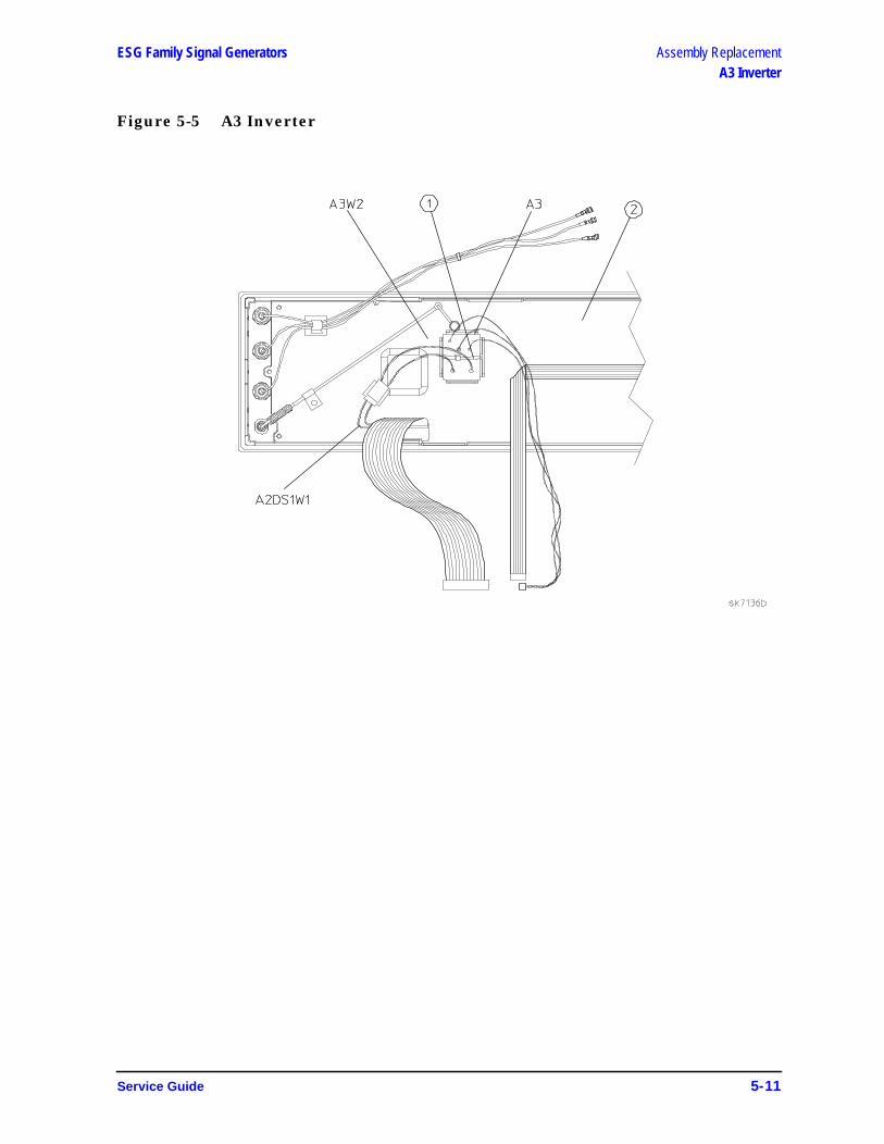
ESG Family Signal Generators Assembly ReplacementA3 Inverter
Figure 5-5 A3 Inverter
Service Guide 5-11

Assembly Replacement ESG Family Signal GeneratorsA4 Power Supply
A4 Power Supply
Tools Required
• T-10 TORX screwdriver
• T-15 TORX screwdriver
Removal
1. Remove the rear panel assembly. (Refer to the “Rear Panel” replacement procedure onpage 5-66.)
2. Remove the screw (item 1 in Figure 5-6) that attaches the CPU/motherboard (A14) tothe bottom of the power supply shield (item 2).
3. Disconnect A4W1 from the CPU/motherboard (A14). (See Figure 5-7 on page 5-14.)
4. Carefully peel off the side trim (item 3) from the left side of the front panel assembly(item 4).
5. Remove the two screws (item 5) that attach the power supply shield (item 2) to the frontpanel assembly.
6. Remove the five screws (item 6) that attach the power supply shield to the instrumentchassis (item 7).
7. Lift the rear of the power supply shield one-quarter inch and then pull it away from theinstrument chassis.
NOTE While removing the power supply shield, try to limit the movement of thefront panel assembly. This will reduce the stress on W9.
8. Remove the 12 screws (item 8) that attach the power supply to the power supply shield.
9. Remove the power supply (A4) from the front end of the shield.
NOTE Before proceeding to the next step ensure that the instrument is fullysupported on a flat surface. This will keep the front panel assembly stableduring the time it is attached only to the right side of the instrument.
Replacement
1. Reverse the removal procedure and do the following:
• Torque all T-10 TORX screws to 9 in-lbs.
• Torque all T-15 TORX screws to 21 in-lbs.
5-12 Service Guide

ESG Family Signal Generators Assembly ReplacementA4 Power Supply
Figure 5-6 A4 Power Supply (1 of 2)
Service Guide 5-13

Assembly Replacement ESG Family Signal GeneratorsA4 Power Supply
Figure 5-7 A4 Power Supply (2 of 2)
5-14 Service Guide
ESG Family Signal Generators Assembly ReplacementA4 Power Supply (with Option 1EM)
A4 Power Supply (with Option 1EM)
Tools Required
• T-10 TORX screwdriver
Removal
1. Remove the front panel assembly. (Refer to the “Front Panel” replacement procedure onpage 5-60.)
2. Remove the bottom cover by removing the 15 screws that secure it.
3. Remove the screw (item 1 in Figure 5-8) that attaches the CPU/motherboard (A14) tothe bottom of the power supply shield (item 2).
4. Disconnect A16W1 from the power supply (A4).
5. Remove the two screws (item 3) that attach the line module (A16) to the rear panel.
6. Remove the line module and A16W1 from the opening in the rear panel. The linemodule will remain connected to the rear panel, however, via the ground wire, A16W2.(See Figure 5-9 on page 5-17.)
7. Remove the three screws (item 4 in Figure 5-8) that attach the rear panel to the powersupply shield.
8. Disconnect A4W1 from the CPU/motherboard (A14). (See Figure 5-9 on page 5-17.)
9. Remove the five screws (item 5) that attach the power supply shield (item 2) to theinstrument chassis (item 6).
10.Pull the power supply shield away from the instrument chassis.
11.Remove the 12 screws (item 7) that attach the power supply to the power supply shield.
12.Remove the power supply (A4) from the front end of the shield.
Replacement
1. Reverse the removal procedure and torque all T-10 TORX screws to 9 in-lbs.
Service Guide 5-15

Assembly Replacement ESG Family Signal GeneratorsA4 Power Supply (with Option 1EM)
Figure 5-8 A4 Power Supply (with Option 1EM) (1 of 2)
5-16 Service Guide
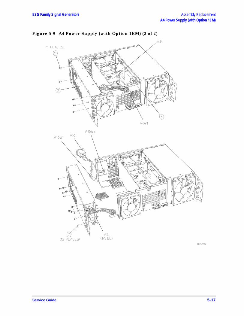
ESG Family Signal Generators Assembly ReplacementA4 Power Supply (with Option 1EM)
Figure 5-9 A4 Power Supply (with Option 1EM) (2 of 2)
Service Guide 5-17

Assembly Replacement ESG Family Signal GeneratorsA14 CPU/Motherboard
A14 CPU/Motherboard
Tools Required
• T-10 TORX screwdriver
• EEPROM extraction tool (Part Number 8710-1982)
Removal
1. Remove the rear panel assembly. (Refer to the “Rear Panel” replacement procedure onpage 5-66 or, if you have Option 1EM, refer to the “Rear Panel (with Option 1EM)”replacement procedure on page 5-70.)
2. Remove all of the boards in the digital card cage (if installed for your model). (Refer tothe “Digital Card Cage Boards” replacement procedure on page 5-58.)
3. Disconnect A1W1, A3W1, A4W1, B1W1, B2W1, W10, and W13 from theCPU/motherboard (A14). (See Figure 5-10.)
4. Disconnect A14Q501 from the CPU/Motherboard.
If A14Q501 is attached to the back of the CPU/Motherboard (as it is in older models),this step is not necessary.
5. If you have Option UNB, also disconnect A19W1 from the CPU/motherboard.
If you have Option 1E6, also disconnect A25W1 from the CPU/motherboard.
6. If you have an ESG-A Series or ESG-AP Series signal generator, go to step 7.
If you have an ESG-D Series or ESG-DP Series signal generator, disconnect W25 andW26 from the CPU/motherboard (A14).
For all current models, disconnect W3, W4, and W5 from the CPU/motherboard,otherwise go to step 7.
NOTE Figure 5-10 represents an Option UN7/UND.
5-18 Service Guide

ESG Family Signal Generators Assembly ReplacementA14 CPU/Motherboard
Figure 5-10 A14 CPU/Motherboard (1 of 3)
Service Guide 5-19

Assembly Replacement ESG Family Signal GeneratorsA14 CPU/Motherboard
7. Turn the signal generator upside-down and remove the screw (item 1 in Figure 5-11)from the CPU/motherboard (A14).
8. Remove the screw (item 2) from the CPU/motherboard.
NOTE In some models, this screw secures transistor A14Q501 to the chassis. In thiscase, the screw is installed with an insulator bushing. Be careful not to lose itwhen removing the screw.
9. Remove the CPU/motherboard.
10.Notice how the jumper connections are set for P104, P105, and P106. (You will need thisinformation when you replace the board.) (See Figure 5-12.) Some CPU/motherboardsdo not have these components.
11.If the CPU/motherboard includes removable devices in locations U106 and U107, labeleach device and remove them using the extraction tool. (See Figure 5-12.)
Replacement
1. Insert U106 and U107 into their respective sockets on the replacementCPU/motherboard.
CAUTION U106 and U107 hold critical data including the serial number, optionconfiguration, and calibration information. You must transfer these devices tothe new CPU/motherboard for the signal generator to work.
2. Reverse the removal procedure and do the following:
• When reinstalling the CPU/motherboard, remember to insert the tab anddaughterboard connector into the corresponding slots of the instrument chassisbefore securing it with the screws.
• Torque the two T-10 TORX screws to 9 in-lbs.
• Refer to replaceable parts chapter for your signal generator model to verify that thecables are reconnected in the correct locations. (Refer to Chapter 3 for the ESG-Aand ESG-D series, refer to Chapter 4 for the ESG-AP and ESG-DP series.)
3. On the CPU/motherboard, set the jumpers for P104, P105, and P106 to the samepositions as the previous board. (See Figure 5-12.)
If the previous CPU/motherboard did not have P104, P105, and P106, set the jumpersto the − position.
4. If you do not know how the jumpers for P104, P105, and P106 were set on the previousCPU/motherboard, do the following:
a. On the CPU/motherboard, set the jumpers for P104, P105, and P106 to the+ position.
5-20 Service Guide
ESG Family Signal Generators Assembly ReplacementA14 CPU/Motherboard
CAUTION Damage can occur to the CPU/motherboard if the signal generator remainsturned on for a prolonged period with the jumpers for P104, P105, and P106positioned incorrectly.
b. Turn the signal generator on, and observe the display.
c. If the display does not show text or characters within five seconds, turn the signalgenerator off and move the jumpers for P104, P105, and P106 to the − position.Repeat the previous step.
5. On the A14 CPU/motherboard, set switch #4 on switch pack S201 to the correct positionfor your display:
If P104, P105, and P106 are set to the + position, set switch #4 of S201 to the up (open)position, away from the CPU/motherboard. (See Figure 5-12.)
If P104, P105, and P106 are set to the − position, set switch #4 of S201 to the down(closed) position, toward the CPU/motherboard. (See Figure 5-12.)
NOTE Switch #5 of S201 is set to the up (open) position in all circumstances.
NOTE You must reset the signal generator for the switch settings to take effect.
Service Guide 5-21

Assembly Replacement ESG Family Signal GeneratorsA14 CPU/Motherboard
Figure 5-11 A14 CPU/Motherboard (2 of 3)
5-22 Service Guide

ESG Family Signal Generators Assembly ReplacementA14 CPU/Motherboard
Figure 5-12 A14 CPU/Motherboard (3 of 3)
Service Guide 5-23
Assembly Replacement ESG Family Signal GeneratorsA14BT1 Battery
A14BT1 Battery
Tools Required
• T-10 TORX screwdriver
• soldering tools
• utility knife
• Dow Corning 3145 RTV Clear Adhesive Sealant (part number 0470-0450)
Removal
1. Remove the instrument cover. (Refer to the “Instrument Cover” replacement procedureon page 5-64.)
2. Remove the top cover by removing the 11 screws that secure it.
3. Remove the bottom cover by removing the 15 screws that secure it.
4. Unsolder the leads of the battery (A14BT1) from the CPU/motherboard (A14).(See Figure 5-13.)
CAUTION Calibration data will be preserved with the removal of the battery. However,user data will be lost unless it is saved and later restored using an externalcontroller.
5. The battery is also attached to the CPU/motherboard with a silicon adhesive. Using autility knife, carefully cut through the adhesive to lift and remove the battery from theCPU/motherboard.
WARNING Battery A14BT1 contains lithium. Do not incinerate or puncture thisbattery. Dispose of the discharged battery in a safe manner. Refer toChapter 7, “Safety and Regulatory,” for instructions on how todispose of the battery.
6. Remove any excess adhesive from the CPU/motherboard surface.
Replacement
WARNING Danger of explosion if battery if incorrectly replaced. Replace onlywith the same or equivalent type recommended. Discard usedbatteries according to manufacturer’s instructions.
1. Apply a small amount of silicon adhesive to the battery’s location on theCPU/motherboard.
2. Insert the new battery into the CPU/motherboard making sure it is oriented with thecorrect polarity.
3. Solder the battery’s leads to the CPU/motherboard.
5-24 Service Guide

ESG Family Signal Generators Assembly ReplacementA14BT1 Battery
4. Reassemble the instrument.
Figure 5-13 A14BT1 Battery
Service Guide 5-25

Assembly Replacement ESG Family Signal GeneratorsA14Q501 Transistor
A14Q501 Transistor
Tools Required
• T-10 TORX screwdriver
Removal
1. Remove the instrument cover. (Refer to the “Instrument Cover” replacement procedureon page 5-64.)
2. Disconnect the transistor assembly (item 1 in Figure 5-14) leads from theCPU/motherboard (A14).
3. Remove the screw (item 2) that attaches the transistor assembly to the chassis.
4. Remove the transistor assembly (item 1), the shoulder washer (item 3), and, ifnecessary, the insulator pad (item 4).
Replacement
1. Reverse the removal procedure and torque the T-10 TORX screw to 9 in-lbs.
5-26 Service Guide
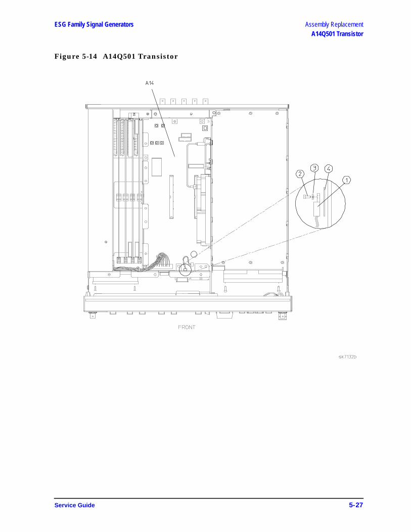
ESG Family Signal Generators Assembly ReplacementA14Q501 Transistor
Figure 5-14 A14Q501 Transistor
Service Guide 5-27

Assembly Replacement ESG Family Signal GeneratorsA15 Daughterboard
A15 Daughterboard
Tools Required
• T-8 TORX screwdriver
• T-10 TORX screwdriver
• long nose pliers
Removal
1. Remove the instrument cover. (Refer to the “Instrument Cover” replacement procedureon page 5-64.)
2. Remove the top cover by removing the 11 screws that secure it.
3. Remove all of the flexible cables connected to the daughterboard (A15).(See Figure 5-15.)
4. Remove the right-side cover (not shown) by first removing the four screws that attach itto the instrument chassis. Then push down on the cover while sliding it towards thefront of the instrument to unhook its tabs from the slots on the top of the chassis.
5-28 Service Guide

ESG Family Signal Generators Assembly ReplacementA15 Daughterboard
Figure 5-15 A15 Daughterboard (1 of 2)
Service Guide 5-29
Assembly Replacement ESG Family Signal GeneratorsA15 Daughterboard
5. Simultaneously lift the left and right extractors (item 1 in Figure 5-16) on each of thedaughterboard card cage boards, and remove them from the card cage slots.
NOTE Figure 5-16 shows an ESG-A or ESG-D series instrument. ESG-AP andESG-DP series instruments contain four boards in the daughterboard cardcage.
6. Remove the five screws (item 2) that attach the daughterboard (A15) to the instrumentchassis.
7. Remove the daughterboard.
Replacement
1. Reverse the removal procedure and do the following:
• Torque all T-8 TORX screws to 9 in-lbs.
• Torque all T-10 TORX screws to 9 in-lbs.
• Refer to replaceable parts chapter for your signal generator model to verify that thecables are reconnected in the correct locations. (Refer to Chapter 3 for the ESG-Aand ESG-D series, refer to Chapter 4 for the ESG-AP and ESG-DP series.)
5-30 Service Guide
ESG Family Signal Generators Assembly ReplacementA15 Daughterboard
Figure 5-16 A15 Daughterboard (2 of 2)
Service Guide 5-31

Assembly Replacement ESG Family Signal GeneratorsA16 Line Module
A16 Line Module
Tools Required
• T-10 TORX screwdriver
• 5.5-mm wrench or nut driver
Removal
1. Remove the rear panel assembly. (Refer to the “Rear Panel” replacement procedure onpage 5-66 or, if you have Option 1EM, refer to the “Rear Panel (with Option 1EM)”replacement procedure on page 5-70.)
2. Remove the nut (item 1 in Figure 5-17) that attaches the line module’s ground wire(A16W2) to the inside of the rear panel.
3. Remove the two screws (item 2) that attach the line module (A16) to the rear panel.
4. Remove the line module from the opening in the rear panel.
Replacement
1. Reverse the removal procedure and do the following:
• Torque the 5.5-mm nut that attaches the ground wire to the rear panel to 9 in-lbs.
• Torque all T-10 TORX screws to 9 in-lbs.
5-32 Service Guide

ESG Family Signal Generators Assembly ReplacementA16 Line Module
Figure 5-17 A16 Line Module
Service Guide 5-33

Assembly Replacement ESG Family Signal GeneratorsA17 and A18 Rear Panel Interface Boards
A17 and A18 Rear Panel Interface Boards
Tools Required
• 5/8-inch wrench or nut driver
• 1/4-inch wrench or nut driver (Option 1EM)
Removal
1. Remove the rear panel assembly. (Refer to the “Rear Panel” replacement procedure onpage 5-66 or, if you have Option 1EM, refer to the “Rear Panel (with Option 1EM)”replacement procedure on page 5-70.)
2. Depending on the option of your signal generator, do the following: (See Figure 5-18.)
Options UN3, UN4, UN8. Remove the nuts (item 1) and washers (item 2) on theeight BNC connectors of the rear panel. Remove the rear panel interface board (A17)from the rear panel.
Options 1EM/UN3, 1EM/UN4, 1EM/UN8. Remove the nuts (item 3) and washers(item 4) on eight of the associated SMB connectors on the rear panel. Remove therear panel interface board (A17) from the rear panel.
Option UN7. Remove the nuts (item 5) and washers (item 6) on five of theassociated SMB connectors on the rear panel. Remove the BER rear panel interfaceboard (A18) from the rear panel.
Replacement
1. Reverse the removal procedure and do the following:
• Torque the 5/8-inch BNC nuts to 21 in-lbs.
• If you have Option 1EM, torque the 1/4-inch SMB nuts to 14 in-lbs.
5-34 Service Guide
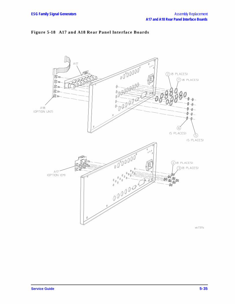
ESG Family Signal Generators Assembly ReplacementA17 and A18 Rear Panel Interface Boards
Figure 5-18 A17 and A18 Rear Panel Interface Boards
Service Guide 5-35

Assembly Replacement ESG Family Signal GeneratorsA19 Reverse Power Protection (RPP)
A19 Reverse Power Protection (RPP)
Tools Required
• T-10 TORX screwdriver
• 5/16-inch open-end wrench
Removal
1. Remove the instrument cover. (Refer to the “Instrument Cover” replacement procedureon page 5-64.)
2. Remove the top cover by removing the 11 screws that secure it.
3. If you have Option 1E6, disconnect W45 and W47 from the pulse modulator (A25) andA25W1 from the CPU/motherboard (A14). (See Figure 5-19.)
If you do not have Option 1E6, disconnect W14 from the mechanical attenuator (AT1).(See Figure 5-20.)
4. Disconnect A19W1 from the CPU/motherboard.
5. Disconnect W9 from the RPP (A19).
6. Disconnect W13 from the CPU/motherboard.
7. Remove the two screws (item 1) that attach the attenuator/RPP assembly to theinstrument chassis.
8. Tilt the assembly away from the chassis wall, then carefully lift it out of the instrument.
NOTE There are two hinged tabs at the bottom of the attenuator/RPP assembly thatfit into slots in the instrument chassis. Therefore, it is necessary to tilt theassembly away from the chassis wall so that the tabs can be guided out of theslots.
9. Disconnect W20 from the RPP and the mechanical attenuator (AT1).
10.If you have Option 1E6, disconnect W46 from the pulse modulator and the mechanicalattenuator. (See Figure 5-19.)
11.Remove the four screws (item 2 in Figure 5-21) that attach the RPP bracket (item 3) tothe attenuator bracket (item 4).
12.Remove the three screws (item 5) that attach the RPP bracket to the RPP.
5-36 Service Guide
ESG Family Signal Generators Assembly ReplacementA19 Reverse Power Protection (RPP)
Replacement
1. Reverse the removal procedure and do the following:
• When reinstalling the electronic attenuator/RPP assembly, remember to insert itshinged tabs into the slots located at the base of the chassis wall on which theassembly will be mounted.
• Torque all semi-rigid cables to 9 in-lbs.
• Torque all screws to 9 in-lbs.
Figure 5-19 A19 Reverse Power Protection (RPP) (1 of 3)
Service Guide 5-37
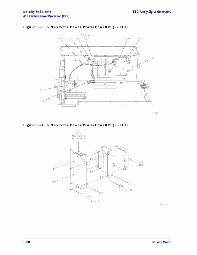
Assembly Replacement ESG Family Signal GeneratorsA19 Reverse Power Protection (RPP)
Figure 5-20 A19 Reverse Power Protection (RPP) (2 of 3)
Figure 5-21 A19 Reverse Power Protection (RPP) (3 of 3)
5-38 Service Guide
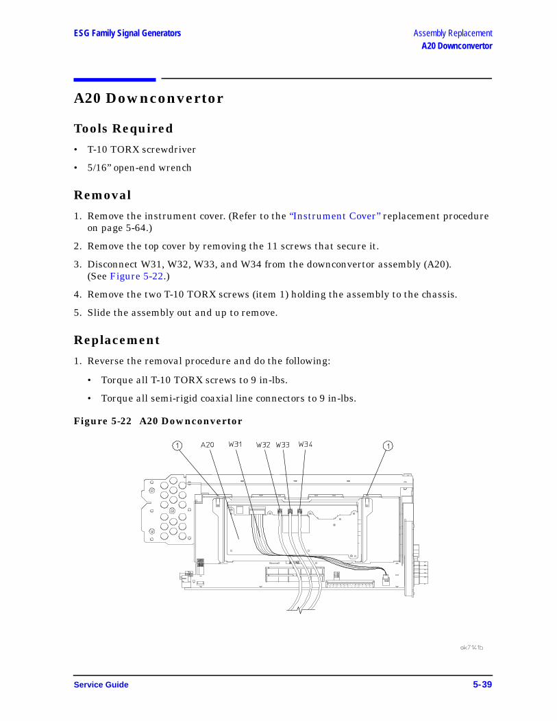
ESG Family Signal Generators Assembly ReplacementA20 Downconvertor
A20 Downconvertor
Tools Required
• T-10 TORX screwdriver
• 5/16” open-end wrench
Removal
1. Remove the instrument cover. (Refer to the “Instrument Cover” replacement procedureon page 5-64.)
2. Remove the top cover by removing the 11 screws that secure it.
3. Disconnect W31, W32, W33, and W34 from the downconvertor assembly (A20).(See Figure 5-22.)
4. Remove the two T-10 TORX screws (item 1) holding the assembly to the chassis.
5. Slide the assembly out and up to remove.
Replacement
1. Reverse the removal procedure and do the following:
• Torque all T-10 TORX screws to 9 in-lbs.
• Torque all semi-rigid coaxial line connectors to 9 in-lbs.
Figure 5-22 A20 Downconvertor
Service Guide 5-39
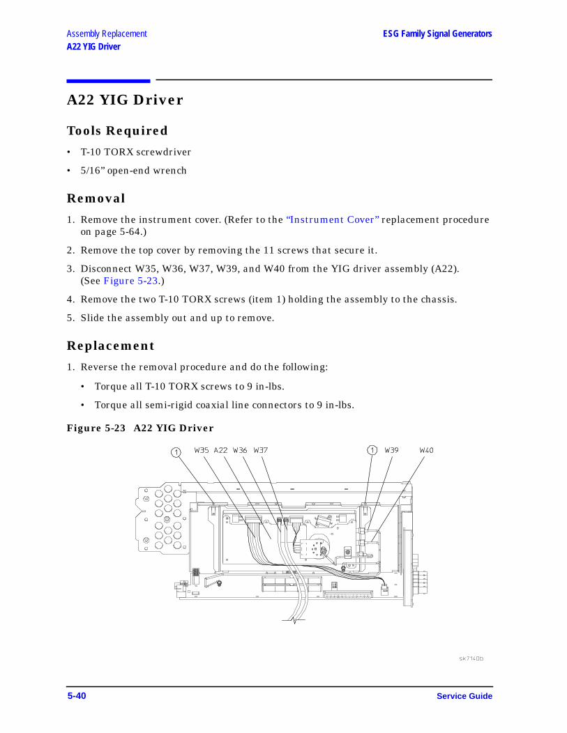
Assembly Replacement ESG Family Signal GeneratorsA22 YIG Driver
A22 YIG Driver
Tools Required
• T-10 TORX screwdriver
• 5/16” open-end wrench
Removal
1. Remove the instrument cover. (Refer to the “Instrument Cover” replacement procedureon page 5-64.)
2. Remove the top cover by removing the 11 screws that secure it.
3. Disconnect W35, W36, W37, W39, and W40 from the YIG driver assembly (A22).(See Figure 5-23.)
4. Remove the two T-10 TORX screws (item 1) holding the assembly to the chassis.
5. Slide the assembly out and up to remove.
Replacement
1. Reverse the removal procedure and do the following:
• Torque all T-10 TORX screws to 9 in-lbs.
• Torque all semi-rigid coaxial line connectors to 9 in-lbs.
Figure 5-23 A22 YIG Driver
5-40 Service Guide
ESG Family Signal Generators Assembly ReplacementA25 Pulse Modulator
A25 Pulse Modulator
Tools Required
• T-10 TORX screwdriver
• 5/16” open-end wrench
Removal
1. Remove the instrument cover. (Refer to the “Instrument Cover” replacement procedureon page 5-64.)
2. Remove the top cover by removing the 11 screws that secure it.
3. Disconnect W45, W46, and W47 from the pulse modulator assembly (A25).(See Figure 5-24.)
4. Disconnect A25W1 from the CPU/motherboard (A14).
5. Remove the two screws (item 1) holding the pulse modulator assembly to the electronicattenuator assembly (AT1).
6. Slide the assembly out and up to remove.
7. Remove the two screws (item 2 in Figure 5-25) that attach the bracket (item 3) to thepulse modulator.
Replacement
1. Reverse the removal procedure and do the following:
• Torque all screws to 9 in-lbs.
• Torque all semi-rigid cables to 9 in-lbs.
Service Guide 5-41

Assembly Replacement ESG Family Signal GeneratorsA25 Pulse Modulator
Figure 5-24 A25 Pulse Modulator (1 of 2)
Figure 5-25 A25 Pulse Modulator (2 of 2)
5-42 Service Guide

ESG Family Signal Generators Assembly ReplacementA25 Pulse Modulator (with Option UNB)
A25 Pulse Modulator (with Option UNB)
Tools Required
• T-10 TORX screwdriver
• 5/16” open-end wrench
Removal
1. Remove the instrument cover. (Refer to the “Instrument Cover” replacement procedureon page 5-64.)
2. Remove the top cover by removing the 11 screws that secure it.
3. Disconnect W45 and W47 from the pulse modulator (A25) and A25W1 from theCPU/motherboard (A14). (See Figure 5-26.)
4. Disconnect A19W1 from the CPU/motherboard.
5. Disconnect W9 from the RPP (A19).
6. Disconnect W13 from the CPU/motherboard.
7. Remove the two screws (item 1) that attach the attenuator/RPP/pulse assembly to theinstrument chassis.
8. Tilt the assembly away from the chassis wall, then carefully lift it out of the instrument.
NOTE There are two hinged tabs at the bottom of the attenuator/RPP/pulseassembly that fit into slots in the instrument chassis. Therefore, it isnecessary to tilt the assembly away from the chassis wall so that the tabs canbe guided out of the slots.
9. Disconnect W20 from the RPP and the mechanical attenuator (AT1).
10.Disconnect W46 from the pulse modulator and the mechanical attenuator.
11.Remove the four screws (item 2 in Figure 5-27) that attach the RPP bracket (item 3) tothe attenuator bracket (item 4).
12.Remove the two screws (item 5) that attach the RPP bracket to the pulse modulator.
Service Guide 5-43

Assembly Replacement ESG Family Signal GeneratorsA25 Pulse Modulator (with Option UNB)
Replacement
1. Reverse the removal procedure and do the following:
• When reinstalling the attenuator/RPP/pulse assembly, remember to insert its hingedtabs into the slots located at the base of the chassis wall on which the assembly willbe mounted.
• Torque all semi-rigid cables to 9 in-lbs.
• Torque all screws to 9 in-lbs.
Figure 5-26 A25 Pulse Modulator (with Option UNB) (1 of 2)
5-44 Service Guide

ESG Family Signal Generators Assembly ReplacementA25 Pulse Modulator (with Option UNB)
Figure 5-27 A25 Pulse Modulator (with Option UNB) (2 of 2)
Service Guide 5-45

Assembly Replacement ESG Family Signal GeneratorsAT1 Electronic Attenuator/RPP
AT1 Electronic Attenuator/RPP
Tools Required
• T-10 TORX screwdriver
• 5/16-inch open-end wrench
Removal
1. Remove the instrument cover. (Refer to the “Instrument Cover” replacement procedureon page 5-64.)
2. Remove the top cover by removing the 11 screws that secure it.
3. If you have Option 1E6, remove the pulse modulator assembly (A25). (Refer to the“A25 Pulse Modulator” replacement procedure on page 5-41.)
4. Disconnect W9, W13, and W14 from the electronic attenuator/RPP (AT1).(See Figure 5-28.)
5. Remove the two screws (item 1) that attach the attenuator/RPP to the instrumentchassis.
6. Tilt the attenuator/RPP away from the chassis wall, then carefully lift it out of theinstrument.
NOTE There are two hinged tabs at the bottom of the attenuator/RPP that fit intoslots in the instrument chassis. Therefore, it is necessary to tilt theattenuator/RPP away from the chassis wall so that the tabs can be guided outof the slots.
Replacement
1. Reverse the removal procedure and do the following:
• When reinstalling the electronic attenuator/RPP (AT1), remember to insert itshinged tabs into the slots located at the base of the chassis wall on which theattenuator/RPP will be mounted.
• Torque W9 and W14 to 9 in-lbs.
• Torque the two T-10 TORX screws to 9 in-lbs.
5-46 Service Guide

ESG Family Signal Generators Assembly ReplacementAT1 Electronic Attenuator/RPP
Figure 5-28 AT1 Electronic Attenuator/RPP
Service Guide 5-47
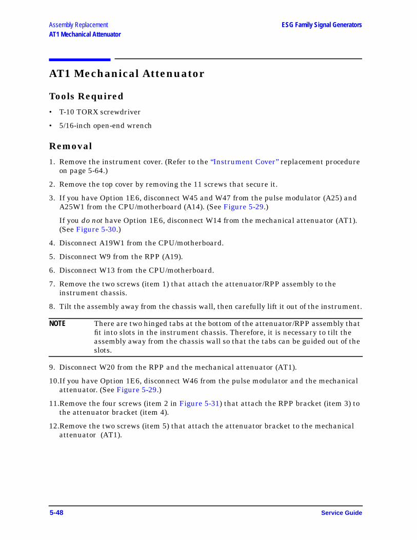
Assembly Replacement ESG Family Signal GeneratorsAT1 Mechanical Attenuator
AT1 Mechanical Attenuator
Tools Required
• T-10 TORX screwdriver
• 5/16-inch open-end wrench
Removal
1. Remove the instrument cover. (Refer to the “Instrument Cover” replacement procedureon page 5-64.)
2. Remove the top cover by removing the 11 screws that secure it.
3. If you have Option 1E6, disconnect W45 and W47 from the pulse modulator (A25) andA25W1 from the CPU/motherboard (A14). (See Figure 5-29.)
If you do not have Option 1E6, disconnect W14 from the mechanical attenuator (AT1).(See Figure 5-30.)
4. Disconnect A19W1 from the CPU/motherboard.
5. Disconnect W9 from the RPP (A19).
6. Disconnect W13 from the CPU/motherboard.
7. Remove the two screws (item 1) that attach the attenuator/RPP assembly to theinstrument chassis.
8. Tilt the assembly away from the chassis wall, then carefully lift it out of the instrument.
NOTE There are two hinged tabs at the bottom of the attenuator/RPP assembly thatfit into slots in the instrument chassis. Therefore, it is necessary to tilt theassembly away from the chassis wall so that the tabs can be guided out of theslots.
9. Disconnect W20 from the RPP and the mechanical attenuator (AT1).
10.If you have Option 1E6, disconnect W46 from the pulse modulator and the mechanicalattenuator. (See Figure 5-29.)
11.Remove the four screws (item 2 in Figure 5-31) that attach the RPP bracket (item 3) tothe attenuator bracket (item 4).
12.Remove the two screws (item 5) that attach the attenuator bracket to the mechanicalattenuator (AT1).
5-48 Service Guide

ESG Family Signal Generators Assembly ReplacementAT1 Mechanical Attenuator
Replacement
1. Reverse the removal procedure and do the following:
• When reinstalling the electronic attenuator/RPP assembly, remember to insert itshinged tabs into the slots located at the base of the chassis wall on which theassembly will be mounted.
• Torque all semi-rigid cables to 9 in-lbs.
• Torque all screws to 9 in-lbs.
Figure 5-29 AT1 Mechanical Attenuator (1 of 3)
Service Guide 5-49
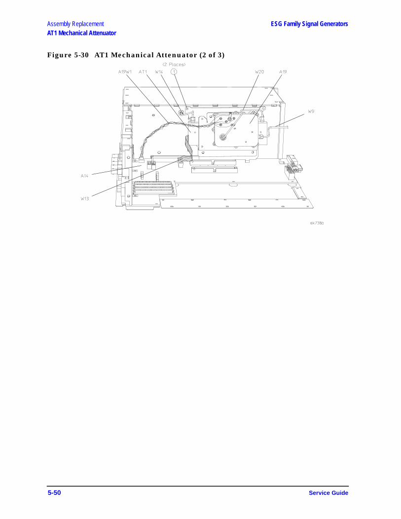
Assembly Replacement ESG Family Signal GeneratorsAT1 Mechanical Attenuator
Figure 5-30 AT1 Mechanical Attenuator (2 of 3)
5-50 Service Guide
ESG Family Signal Generators Assembly ReplacementAT1 Mechanical Attenuator
Figure 5-31 AT1 Mechanical Attenuator (3 of 3)
Service Guide 5-51
Assembly Replacement ESG Family Signal GeneratorsB1 Small Fan
B1 Small Fan
Tools Required
• knife blade (or equivalent)
• long nose pliers
Removal
NOTE It is best to attempt this procedure without removing the front panelassembly. If the front panel assembly is removed, you will be required toperform time-consuming “Power Level Accuracy” verification tests andadjustments.
1. Remove the instrument cover. (Refer to the “Instrument Cover” replacement procedureon page 5-64.)
2. Disconnect B1W1 from the CPU/motherboard (A14). (See Figure 5-32.)
3. Remove the four plastic rivets (item 1) that attach the fan assembly (B1) to theinstrument chassis. Use a knife blade (or equivalent) to pry up the head of the plungerportion of the rivet. Once the head of the plunger is adequately raised, use a pair of longnose pliers to remove the rivet. Be careful not to damage the rivets with the blade.
NOTE The plastic rivets consist of two pieces: a plunger and a sheath. Ensure bothparts are removed.
4. Remove the fan assembly.
Replacement
1. Reverse the removal procedure. When reinserting the plastic rivets, the sheath must befully seated in the fan assembly before the plunger can be depressed.
5-52 Service Guide

ESG Family Signal Generators Assembly ReplacementB1 Small Fan
Figure 5-32 B1 Small Fan
Service Guide 5-53
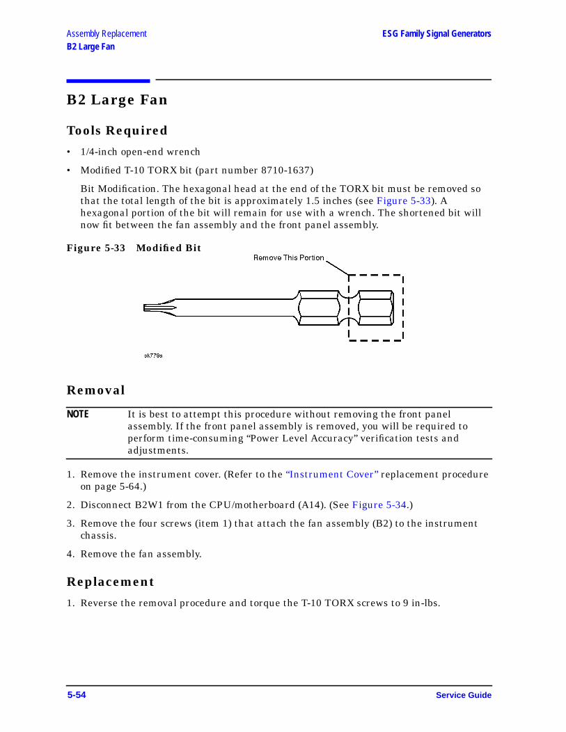
Assembly Replacement ESG Family Signal GeneratorsB2 Large Fan
B2 Large Fan
Tools Required
• 1/4-inch open-end wrench
• Modified T-10 TORX bit (part number 8710-1637)
Bit Modification. The hexagonal head at the end of the TORX bit must be removed sothat the total length of the bit is approximately 1.5 inches (see Figure 5-33). Ahexagonal portion of the bit will remain for use with a wrench. The shortened bit willnow fit between the fan assembly and the front panel assembly.
Figure 5-33 Modified Bit
Removal
NOTE It is best to attempt this procedure without removing the front panelassembly. If the front panel assembly is removed, you will be required toperform time-consuming “Power Level Accuracy” verification tests andadjustments.
1. Remove the instrument cover. (Refer to the “Instrument Cover” replacement procedureon page 5-64.)
2. Disconnect B2W1 from the CPU/motherboard (A14). (See Figure 5-34.)
3. Remove the four screws (item 1) that attach the fan assembly (B2) to the instrumentchassis.
4. Remove the fan assembly.
Replacement
1. Reverse the removal procedure and torque the T-10 TORX screws to 9 in-lbs.
5-54 Service Guide

ESG Family Signal Generators Assembly ReplacementB2 Large Fan
Figure 5-34 B2 Large Fan
Service Guide 5-55

Assembly Replacement ESG Family Signal GeneratorsDaughterboard Card Cage Boards
Daughterboard Card Cage BoardsUse this procedure to remove any of the following assemblies: (See Figure 5-35.)
• Output Board (A9)
• Reference Board (A11)
• Synthesizer/Doubler Board (A12)
• Sampler Board (A23)
• Frac-N/Divider Board (A24)
Tools Required
• T-8 TORX screwdriver
Removal
1. Remove the instrument cover. (Refer to the “Instrument Cover” replacement procedureon page 5-64.)
2. Remove the right-side cover by removing the four screws that attach it to theinstrument chassis.
3. Simultaneously lift the left and right extractors (item 1) on the board you want toremove.
4. Remove the board from the card cage slot.
Replacement
1. Reverse the removal procedure and torque all T-8 TORX screws to 9 in-lbs.
5-56 Service Guide

ESG Family Signal Generators Assembly ReplacementDaughterboard Card Cage Boards
Figure 5-35 Daughterboard Card Cage Boards
Service Guide 5-57
Assembly Replacement ESG Family Signal GeneratorsDigital Card Cage Boards
Digital Card Cage BoardsUse this procedure to remove any of the following assemblies: (See Figure 5-36.)
• A5 Dual Arbitrary Waveform Generator Board
• A6 Bit Error Rate Test Board
• A7 Baseband Generator Board
• A8 Data Generator Board
• A21 Demodulator Board
Tools Required
• T-10 TORX screwdriver
• long nose pliers
Removal
1. Remove the instrument cover. (Refer to the “Instrument Cover” replacement procedureon page 5-64.)
2. Remove the top cover by removing the 11 screws that secure it.
3. Disconnect all of the cables and harnesses from the board.
4. Pull up on the board to remove it from the CPU/motherboard connector.
Replacement
1. Reverse the removal procedure and do the following:
• Refer to replaceable parts chapter for your signal generator model to verify that thecables are reconnected in the correct locations. (Refer to Chapter 3 for the ESG-Aand ESG-D series, refer to Chapter 4 for the ESG-AP and ESG-DP series.)
• Torque all T-10 TORX screws to 9 in-lbs.
5-58 Service Guide
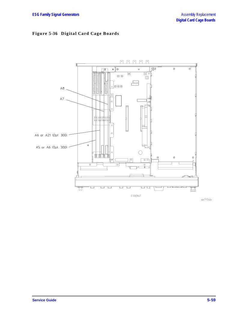
ESG Family Signal Generators Assembly ReplacementDigital Card Cage Boards
Figure 5-36 Digital Card Cage Boards
Service Guide 5-59
Assembly Replacement ESG Family Signal GeneratorsFront Panel
Front Panel
Tools Required
• T-10 TORX screwdriver
• T-15 TORX screwdriver
• 5/16-inch open-end wrench
• long nose pliers (used for disconnecting cables from the daughterboard)
Removal
1. Remove the instrument cover. (Refer to the “Instrument Cover” replacement procedureon page 5-64.)
2. Remove the top cover by removing the 11 screws that secure it.
3. Disconnect A1W1, A3W1, and W10 from the CPU/motherboard (A14). (SeeFigure 5-37.) To disconnect W10, you must first unlock the CPU/motherboard connectorby pulling out the locking mechanism (much like pulling out a drawer).
4. Disconnect all remaining front panel cables (if any) from the various assemblies withinthe signal generator.
NOTE Figure 5-37 represents an Option UN3 or UN4.
5-60 Service Guide

ESG Family Signal Generators Assembly ReplacementFront Panel
Figure 5-37 Front Panel (1 of 2)
Service Guide 5-61

Assembly Replacement ESG Family Signal GeneratorsFront Panel
5. Carefully peel off the side trim (item 1 in Figure 5-38) from the sides of the front panelassembly (item 2).
6. Remove the four screws (item 3) that attach the front panel assembly to the instrumentchassis.
7. Pull the front panel assembly away from the instrument chassis.
Replacement
1. Reverse the removal procedure and do the following:
• Refer to replaceable parts chapter for your signal generator model to verify that thecables are reconnected in the correct locations. (Refer to Chapter 3 for the ESG-Aand ESG-D series, refer to Chapter 4 for the ESG-AP and ESG-DP series.)
• To reconnect W10 to its CPU/motherboard connector do the following:
a. Ensure the CPU/motherboard connector is unlocked by pulling out the lockingmechanism (much like pulling out a drawer).
b. Insert W10 into the connector, making sure the conductive contacts are facing up(the blue insulation should be facing down).
c. Lock the connector by pushing in on the locking mechanism.
NOTE Intermittent display problems may result if W10 is not connected correctly.
• Torque W9 to 9 in-lbs.
• Torque all T-10 TORX screws to 9 in-lbs.
• Torque all T-15 TORX screws to 21 in-lbs.
5-62 Service Guide

ESG Family Signal Generators Assembly ReplacementFront Panel
Figure 5-38 Front Panel (2 of 2)
Service Guide 5-63
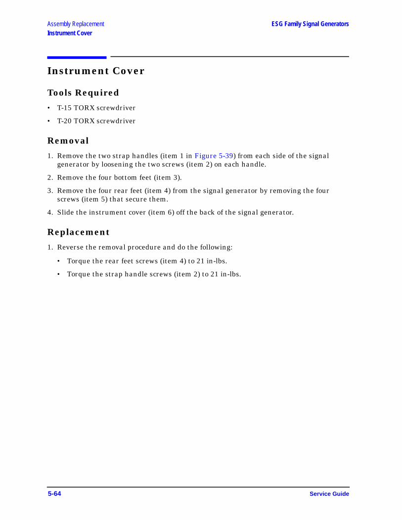
Assembly Replacement ESG Family Signal GeneratorsInstrument Cover
Instrument Cover
Tools Required
• T-15 TORX screwdriver
• T-20 TORX screwdriver
Removal
1. Remove the two strap handles (item 1 in Figure 5-39) from each side of the signalgenerator by loosening the two screws (item 2) on each handle.
2. Remove the four bottom feet (item 3).
3. Remove the four rear feet (item 4) from the signal generator by removing the fourscrews (item 5) that secure them.
4. Slide the instrument cover (item 6) off the back of the signal generator.
Replacement
1. Reverse the removal procedure and do the following:
• Torque the rear feet screws (item 4) to 21 in-lbs.
• Torque the strap handle screws (item 2) to 21 in-lbs.
5-64 Service Guide
ESG Family Signal Generators Assembly ReplacementInstrument Cover
Figure 5-39 Instrument Cover
Service Guide 5-65

Assembly Replacement ESG Family Signal GeneratorsRear Panel
Rear Panel
Tools Required
• T-10 TORX screwdriver
• 3/16-inch wrench or nut driver
• 9/32-inch wrench or nut driver
• 5/16-inch open-end wrench
• 5/8-inch wrench or nut driver
• long nose pliers
Removal
1. Remove the instrument cover. (Refer to the “Instrument Cover” replacement procedureon page 5-64.)
2. Remove the top cover by removing the 11 screws that secure it.
3. Remove the bottom cover by removing the 15 screws that secure it.
4. Disconnect A16W1 from the power supply (A4). (See Figure 5-40.) A16W1 can beaccessed through an opening on the bottom of the power supply shield (item 1).
5. Disconnect all remaining rear panel cables (if any) from the various assemblies withinthe signal generator.
NOTE Figure 5-40 represents an Option UN7/UND.
5-66 Service Guide

ESG Family Signal Generators Assembly ReplacementRear Panel
Figure 5-40 Rear Panel (1 of 2)
Service Guide 5-67
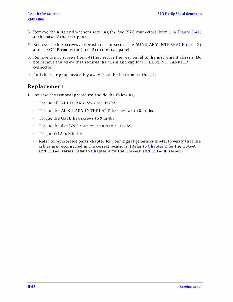
Assembly Replacement ESG Family Signal GeneratorsRear Panel
6. Remove the nuts and washers securing the five BNC connectors (item 1 in Figure 5-41)at the base of the rear panel.
7. Remove the hex screws and washers that secure the AUXILARY INTERFACE (item 2)and the GPIB connector (item 3) to the rear panel.
8. Remove the 10 screws (item 4) that secure the rear panel to the instrument chassis. Donot remove the screw that secures the chain and cap for COHERENT CARRIERconnector.
9. Pull the rear panel assembly away from the instrument chassis.
Replacement
1. Reverse the removal procedure and do the following:
• Torque all T-10 TORX screws to 9 in-lbs.
• Torque the AUXILARY INTERFACE hex screws to 6 in-lbs.
• Torque the GPIB hex screws to 9 in-lbs.
• Torque the five BNC connector nuts to 21 in-lbs.
• Torque W12 to 9 in-lbs.
• Refer to replaceable parts chapter for your signal generator model to verify that thecables are reconnected in the correct locations. (Refer to Chapter 3 for the ESG-Aand ESG-D series, refer to Chapter 4 for the ESG-AP and ESG-DP series.)
5-68 Service Guide
ESG Family Signal Generators Assembly ReplacementRear Panel
Figure 5-41 Rear Panel (2 of 2)
Service Guide 5-69

Assembly Replacement ESG Family Signal GeneratorsRear Panel (with Option 1EM)
Rear Panel (with Option 1EM)
Tools Required
• T-10 TORX screwdriver
• 3/16-inch wrench or nut driver
• 9/32-inch wrench or nut driver
• 5/8-inch wrench or nut driver
• long nose pliers
Removal
1. Remove the instrument cover. (Refer to the “Instrument Cover” replacement procedureon page 5-64.)
2. Remove the top cover by removing the 11 screws that secure it.
3. Remove the bottom cover by removing the 15 screws that secure it.
4. Disconnect A16W1 from the power supply (A4). (See Figure 5-42.) A16W1 can beaccessed through an opening on the bottom of the power supply shield (item 1).
5. Disconnect all remaining rear panel cables from the various assemblies within thesignal generator.
5-70 Service Guide
ESG Family Signal Generators Assembly ReplacementRear Panel (with Option 1EM)
Figure 5-42 Rear Panel (with Option 1EM) (1 of 2)
Service Guide 5-71
Assembly Replacement ESG Family Signal GeneratorsRear Panel (with Option 1EM)
6. Remove the nuts and washers securing the five BNC connectors (item 1 in Figure 5-43)at the base of the rear panel.
7. Remove the hex screws and washers that secure the AUXILARY INTERFACE (item 2)and the GPIB connector (item 3) to the rear panel.
8. Remove the 10 screws (item 4) that secure the rear panel to the instrument chassis.
9. Pull the rear panel assembly away from the instrument chassis.
Replacement
1. Reverse the removal procedure and do the following:
• Torque all T-10 TORX screws to 9 in-lbs.
• Torque the AUXILARY INTERFACE hex screws to 6 in-lbs.
• Torque the GPIB hex screws to 9 in-lbs.
• Torque the five BNC connector nuts to 21 in-lbs.
• Torque W9 and W12 to 9 in-lbs.
• Refer to replaceable parts chapter for your signal generator model to verify that thecables are reconnected in the correct locations. (Refer to Chapter 3 for the ESG-Aand ESG-D series, refer to Chapter 4 for the ESG-AP and ESG-DP series.)
Figure 5-43 Rear Panel (with Option 1EM) (2 of 2)
5-72 Service Guide

ESG Family Signal Generators Assembly ReplacementSemi-Rigid Cables
Semi-Rigid CablesUse this procedure to remove and replace semi-rigid cables that attach to thedaughterboard card cage. If the cable you are removing/replacing does not attach to thedaughterboard card cage, no special instruction is necessary other than step 3 in the“Replacement” section below.
Tools Required
• MILBAR 2R snap-ring pliers (used to remove snap rings from cable retainers)
• 5/16-inch open-end wrench
Removal
1. Remove all the daughterboard card cage boards to allow access to the instrumentchassis cable connections. (Refer to the “Daughterboard Card Cage Boards”replacement procedure on page 5-56.)
2. Remove the snap ring (item 1 in Figure 5-44) from the cable retainer (item 2) of thecable you want to remove. The cable is now disconnected from the instrument chassis(item 3).
3. Disconnect the other end of the cable.
Replacement
1. If you’re installing a new cable, a new cable retainer (item 2) must first be attached tothe end of the cable (item 4). Verify the cable retainer is correctly attached by listeningfor an audible “click” as you slide it over the end of the cable.
2. Insert the cable-retainer end of the cable assembly into the opening of the instrumentchassis and then secure it with a snap ring.
3. Connect the other end of the cable. All semi-rigid cables should be torqued to 9 in-lbs.
4. Replace the daughterboard card cage boards.
Figure 5-44 Semi-Rigid Cables
Service Guide 5-73
ESG Family Signal Generators
6 Post-Repair Procedures
This chapter lists the performance tests and adjustments that must be performed after anassembly has been replaced.
Service Guide 6-1

Post-Repair Procedures ESG Family Signal GeneratorsPerformance Tests
Performance TestsThe tables in this section list the performance tests that must be performed when aspecific assembly is repaired or replaced. (Refer to the list below for the table that appliesto your signal generator.) Except where noted, all tests are automated using software. Formore information on performance tests, refer to the calibration guide.
For the ESG-A Series refer to Table 6-1 on page 6-3.
For the ESG-D Series refer to Table 6-2 on page 6-4.
For the ESG-AP Series refer to Table 6-3 on page 6-5.
For the ESG-DP Series refer to Table 6-4 on page 6-6.
6-2 Service Guide
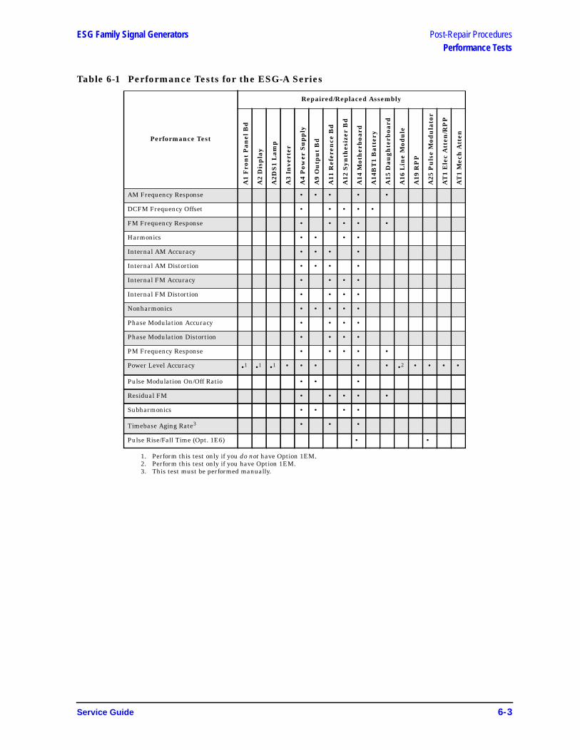
ESG Family Signal Generators Post-Repair ProceduresPerformance Tests
Table 6-1 Performance Tests for the ESG-A Series
Performance Test
Repaired/Replaced Assembly
A1
Fro
nt
Pan
el B
d
A2
Dis
pla
y
A2D
S1
Lam
p
A3
Inve
rter
A4
Pow
er S
up
ply
A9
Ou
tpu
t B
d
A11
Ref
eren
ce B
d
A12
Syn
thes
izer
Bd
A14
Mot
her
boa
rd
A14
BT
1 B
atte
ry
A15
Dau
ghte
rboa
rd
A16
Lin
e M
odu
le
A19
RP
P
A25
Pu
lse
Mod
ula
tor
AT
1 E
lec
Att
en/R
PP
AT
1 M
ech
Att
en
AM Frequency Response • • • • •
DCFM Frequency Offset • • • • •
FM Frequency Response • • • • •
Harmonics • • • •
Internal AM Accuracy • • • •
Internal AM Distortion • • • •
Internal FM Accuracy • • • •
Internal FM Distortion • • • •
Nonharmonics • • • • •
Phase Modulation Accuracy • • • •
Phase Modulation Distortion • • • •
PM Frequency Response • • • • •
Power Level Accuracy •1 •1 •1
1. Perform this test only if you do not have Option 1EM.
• • • • • •2
2. Perform this test only if you have Option 1EM.
• • • •
Pulse Modulation On/Off Ratio • • •
Residual FM • • • • •
Subharmonics • • • •
Timebase Aging Rate3
3. This test must be performed manually.
• • •
Pulse Rise/Fall Time (Opt. 1E6) • •
Service Guide 6-3
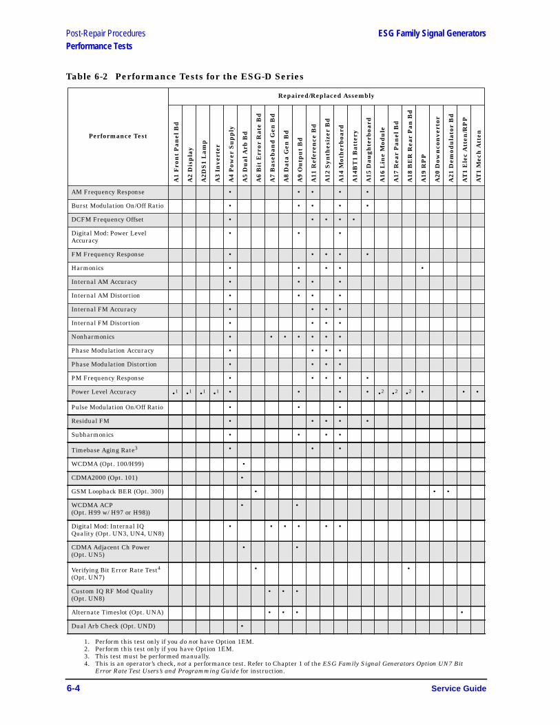
Post-Repair Procedures ESG Family Signal GeneratorsPerformance Tests
Table 6-2 Performance Tests for the ESG-D Series
Performance Test
Repaired/Replaced Assembly
A1
Fro
nt
Pan
el B
d
A2
Dis
pla
y
A2D
S1
Lam
p
A3
Inve
rter
A4
Pow
er S
up
ply
A5
Du
al A
rb B
d
A6
Bit
Err
or R
ate
Bd
A7
Bas
eban
d G
en B
d
A8
Dat
a G
en B
d
A9
Ou
tpu
t B
d
A11
Ref
eren
ce B
d
A12
Syn
thes
izer
Bd
A14
Mot
her
boa
rd
A14
BT
1 B
atte
ry
A15
Dau
ghte
rboa
rd
A16
Lin
e M
odu
le
A17
Rea
r P
anel
Bd
A18
BE
R R
ear
Pan
Bd
A19
RP
P
A20
Dow
nco
nve
rtor
A21
Dem
odu
lato
r B
d
AT
1 E
lec
Att
en/R
PP
AT
1 M
ech
Att
en
AM Frequency Response • • • • •
Burst Modulation On/Off Ratio • • • • •
DCFM Frequency Offset • • • • •
Digital Mod: Power LevelAccuracy
• • •
FM Frequency Response • • • • •
Harmonics • • • • •
Internal AM Accuracy • • • •
Internal AM Distortion • • • •
Internal FM Accuracy • • • •
Internal FM Distortion • • • •
Nonharmonics • • • • • • •
Phase Modulation Accuracy • • • •
Phase Modulation Distortion • • • •
PM Frequency Response • • • • •
Power Level Accuracy •1 •1 •1 •1
1. Perform this test only if you do not have Option 1EM.
• • • • •2 •2
2. Perform this test only if you have Option 1EM.
•2 • • •
Pulse Modulation On/Off Ratio • • •
Residual FM • • • • •
Subharmonics • • • •
Timebase Aging Rate3
3. This test must be performed manually.
• • •
WCDMA (Opt. 100/H99) •
CDMA2000 (Opt. 101) •
GSM Loopback BER (Opt. 300) • • •
WCDMA ACP(Opt. H99 w/ H97 or H98))
• •
Digital Mod: Internal IQQuality (Opt. UN3, UN4, UN8)
• • • • • •
CDMA Adjacent Ch Power(Opt. UN5)
• •
Verifying Bit Error Rate Test4
(Opt. UN7)
4. This is an operator’s check, not a performance test. Refer to Chapter 1 of the ESG Family Signal Generators Option UN7 BitError Rate Test Users’s and Programming Guide for instruction.
• •
Custom IQ RF Mod Quality(Opt. UN8)
• • •
Alternate Timeslot (Opt. UNA) • • • •
Dual Arb Check (Opt. UND) •
6-4 Service Guide

ESG Family Signal Generators Post-Repair ProceduresPerformance Tests
Table 6-3 Performance Tests for the ESG-AP Series
Performance Test
Repaired/Replaced Assembly
A1
Fro
nt
Pan
el B
d
A2
Dis
pla
y
A2D
S1
Lam
p
A3
Inve
rter
A4
Pow
er S
up
ply
A9
Ou
tpu
t B
d
A11
Ref
eren
ce B
d
A14
Mot
her
boa
rd
A14
BT
1 B
atte
ry
A15
Dau
ghte
rboa
rd
A16
Lin
e M
odu
le
A19
RP
P
A22
YO
Dri
ver
A23
Sam
ple
r B
d
A24
Fra
c-N
/Div
ider
Bd
A25
Pu
lse
Mod
ula
tor
AT
1 E
lec
Att
en/R
PP
AT
1 M
ech
Att
en
AM Frequency Response • • • • •
DCFM Frequency Offset • • • • • •
FM Frequency Response • • • • • •
Harmonics • • • • •
Internal AM Accuracy • • • •
Internal AM Distortion • • • •
Internal FM Accuracy • • • • •
Internal FM Distortion • • • • •
Nonharmonics • • • • • • •
Phase Modulation Accuracy • • • • •
Phase Modulation Distortion • • • • •
Phase Noise3 • • • • •
PM Frequency Response • • • • •
Power Level Accuracy •1 •1 •1
1. Perform this test only if you do not have Option 1EM.
• • • • • •2
2. Perform this test only if you have Option 1EM.
• • • • • •
Pulse Modulation On/Off Ratio • • •
Residual FM3 • • • • • •
Timebase Aging Rate3
3. This test must be performed manually.
• • •
Pulse Rise/Fall Time (Opt. 1E6) •
Service Guide 6-5

Post-Repair Procedures ESG Family Signal GeneratorsPerformance Tests
Table 6-4 Performance Tests for the ESG-DP Series
Performance Test
Repaired/Replaced Assembly
A1
Fro
nt
Pan
el B
d
A2
Dis
pla
y
A2D
S1
Lam
p
A3
Inve
rter
A4
Pow
er S
up
ply
A5
Du
al A
rb B
d
A6
Bit
Err
or R
ate
Bd
A7
Bas
eban
d G
en B
d
A8
Dat
a G
en B
d
A9
Ou
tpu
t B
d
A11
Ref
eren
ce B
d
A14
Mot
her
boa
rd
A14
BT
1 B
atte
ry
A15
Dau
ghte
rboa
rd
A16
Lin
e M
odu
le
A17
Rea
r P
anel
Bd
A18
BE
R R
ear
Pan
Bd
A19
RP
P
A22
YO
Dri
ver
A23
Sam
ple
r B
d
A24
Fra
c-N
/Div
ider
Bd
AT
1 E
lec
Att
en/R
PP
AT
1 M
ech
Att
en
AM Frequency Response • • • • •
Burst Modulation On/Off Ratio • • • • •
DCFM Frequency Offset • • • • • •
Digital Mod: Power LevelAccuracy
• • •
FM Frequency Response • • • • • •
Harmonics • • • • •
Internal AM Accuracy • • • •
Internal AM Distortion • • • •
Internal FM Accuracy • • • • •
Internal FM Distortion • • • • •
Nonharmonics • • • • • • • •
Phase Modulation Accuracy • • • • •
Phase Modulation Distortion • • • • •
Phase Noise3 • • • • • • • • •
PM Frequency Response • • • • •
Power Level Accuracy •1 •1 •1 •1
1. Perform this test only if you do not have Option 1EM.
• • • • •2 •2
2. Perform this test only if you have Option 1EM.
•2 • • • • •
Pulse Modulation On/Off Ratio • • •
Residual FM3 • • • • • • • • •
Timebase Aging Rate3
3. This test must be performed manually.
• • •
WCDMA (Opt. 100/H99) •
CDMA2000 (Opt. 101) •
WCDMA ACP(Opt. H99 w/ H97 or H98))
• •
Digital Mod: Internal IQQuality (Opt. UN3, UN4, UN8)
• • • • • •
CDMA Adjacent Ch Power(Opt. UN5)
• •
Verifying Bit Error Rate Test4
(Opt. UN7)
4. This is an operator’s check, not a performance test. Refer to Chapter 1 of the ESG Family Signal Generators Option UN7 BitError Rate Test Users’s and Programming Guide for instruction.
• •
Custom IQ RF Mod Quality(Opt. UN8)
• • •
Alternate Timeslot (Opt. UNA) • • • •
Dual Arb Check (Opt. UND) •
6-6 Service Guide

ESG Family Signal Generators Post-Repair ProceduresAdjustments
AdjustmentsThe tables in this section list the adjustments that must be performed when a specificassembly is repaired or replaced. (Refer to the list below for the table that applies to yoursignal generator.) Except where noted, all adjustments are automated using software. Formore information on adjustments, refer to the calibration guide.
For the ESG-A Series refer to Table 6-5 on page 6-8.
For the ESG-D Series refer to Table 6-6 on page 6-9.
For the ESG-AP Series refer to Table 6-7 on page 6-10.
For the ESG-DP Series refer to Table 6-8 on page 6-11.
Service Guide 6-7
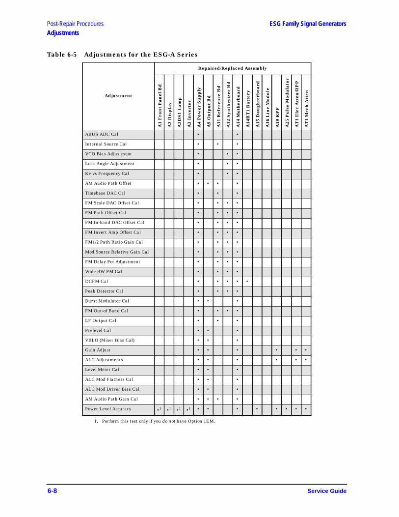
Post-Repair Procedures ESG Family Signal GeneratorsAdjustments
Table 6-5 Adjustments for the ESG-A Series
Adjustment
Repaired/Replaced Assembly
A1
Fro
nt
Pan
el B
d
A2
Dis
pla
y
A2D
S1
Lam
p
A3
Inve
rter
A4
Pow
er S
up
ply
A9
Ou
tpu
t B
d
A11
Ref
eren
ce B
d
A12
Syn
thes
izer
Bd
A14
Mot
her
boa
rd
A14
BT
1 B
atte
ry
A15
Dau
ghte
rboa
rd
A16
Lin
e M
odu
le
A19
RP
P
A25
Pu
lse
Mod
ula
tor
AT
1 E
lec
Att
en/R
PP
AT
1 M
ech
Att
en
ABUS ADC Cal • •
Internal Source Cal • • •
VCO Bias Adjustment • • •
Lock Angle Adjustment • • •
Kv vs Frequency Cal • • •
AM Audio Path Offset • • • •
Timebase DAC Cal • • •
FM Scale DAC Offset Cal • • • •
FM Path Offset Cal • • • •
FM In-band DAC Offset Cal • • • •
FM Invert Amp Offset Cal • • • •
FM1/2 Path Ratio Gain Cal • • • •
Mod Source Relative Gain Cal • • • •
FM Delay Pot Adjustment • • • •
Wide BW PM Cal • • • •
DCFM Cal • • • • •
Peak Detector Cal • • • •
Burst Modulator Cal • • •
FM Out-of Band Cal • • • •
LF Output Cal • • •
Prelevel Cal • • •
VBLO (Mixer Bias Cal) • • •
Gain Adjust • • • • • •
ALC Adjustments • • • • • •
Level Meter Cal • • •
ALC Mod Flatness Cal • • •
ALC Mod Driver Bias Cal • • •
AM Audio Path Gain Cal • • • •
Power Level Accuracy •1 •1 •1 •1
1. Perform this test only if you do not have Option 1EM.
• • • • • • • •
6-8 Service Guide
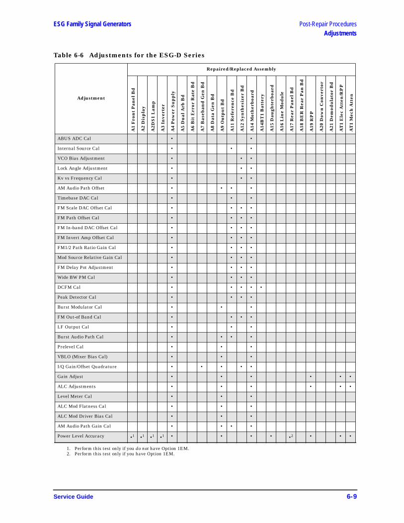
ESG Family Signal Generators Post-Repair ProceduresAdjustments
Table 6-6 Adjustments for the ESG-D Series
Adjustment
Repaired/Replaced Assembly
A1
Fro
nt
Pan
el B
d
A2
Dis
pla
y
A2D
S1
Lam
p
A3
Inve
rter
A4
Pow
er S
up
ply
A5
Du
al A
rb B
d
A6
Bit
Err
or R
ate
Bd
A7
Bas
eban
d G
en B
d
A8
Dat
a G
en B
d
A9
Ou
tpu
t B
d
A11
Ref
eren
ce B
d
A12
Syn
thes
izer
Bd
A14
Mot
her
boa
rd
A14
BT
1 B
atte
ry
A15
Dau
ghte
rboa
rd
A16
Lin
e M
odu
le
A17
Rea
r P
anel
Bd
A18
BE
R R
ear
Pan
Bd
A19
RP
P
A20
Dow
n C
onve
rtor
A21
Dem
odu
lato
r B
d
AT
1 E
lec
Att
en/R
PP
AT
1 M
ech
Att
en
ABUS ADC Cal • •
Internal Source Cal • • •
VCO Bias Adjustment • • •
Lock Angle Adjustment • • •
Kv vs Frequency Cal • • •
AM Audio Path Offset • • • •
Timebase DAC Cal • • •
FM Scale DAC Offset Cal • • • •
FM Path Offset Cal • • • •
FM In-band DAC Offset Cal • • • •
FM Invert Amp Offset Cal • • • •
FM1/2 Path Ratio Gain Cal • • • •
Mod Source Relative Gain Cal • • • •
FM Delay Pot Adjustment • • • •
Wide BW PM Cal • • • •
DCFM Cal • • • • •
Peak Detector Cal • • • •
Burst Modulator Cal • • •
FM Out-of Band Cal • • • •
LF Output Cal • • •
Burst Audio Path Cal • • • •
Prelevel Cal • • •
VBLO (Mixer Bias Cal) • • •
I/Q Gain/Offset Quadrature • • • • •
Gain Adjust • • • • • •
ALC Adjustments • • • • • •
Level Meter Cal • • •
ALC Mod Flatness Cal • • •
ALC Mod Driver Bias Cal • • •
AM Audio Path Gain Cal • • • •
Power Level Accuracy •1 •1 •1 •1
1. Perform this test only if you do not have Option 1EM.
• • • • •2
2. Perform this test only if you have Option 1EM.
• • •
Service Guide 6-9

Post-Repair Procedures ESG Family Signal GeneratorsAdjustments
Table 6-7 Adjustments for the ESG-AP Series
Adjustment
Repaired/Replaced Assembly
A1
Fro
nt
Pan
el B
d
A2
Dis
pla
y
A2D
S1
Lam
p
A3
Inve
rter
A4
Pow
er S
up
ply
A9
Ou
tpu
t B
d
A11
Ref
eren
ce B
d
A14
Mot
her
boa
rd
A14
BT
1 B
atte
ry
A15
Dau
ghte
rboa
rd
A16
Lin
e M
odu
le
A19
RP
P
A22
YO
Dri
ver
A23
Sam
ple
r B
d
A24
Fra
c-N
/Div
ider
Bd
A25
Pu
lse
Mod
ula
tor
AT
1 E
lec
Att
en/R
PP
AT
1 M
ech
Att
en
ABUS ADC Cal • •
Internal Source Cal • • •
VCO Bias Adjustment • • •
Lock Angle Adjustment • • •
Kv vs Frequency Cal • • •
AM Audio Path Offset • • • •
Timebase DAC Cal • • •
FM Scale DAC Offset Cal • • • •
FM Path Offset Cal • • • •
FM In-band DAC Offset Cal • • • •
FM Invert Amp Offset Cal • • • •
FM1/2 Path Ratio Gain Cal • • • •
Mod Source Relative Gain Cal • • • •
FM Delay Pot Adjustment • • • •
Wide BW PM Cal • • • •
DCFM Cal • • • • •
Peak Detector Cal • • • •
Burst Modulator Cal • • •
FM Out-of Band Cal • • • •
LF Output Cal • • •
VBLO (Mixer Bias Cal) • • •
Gain Adjust • • • • • •
ALC Adjustments • • • • • •
Level Meter Cal • • •
ALC Mod Flatness Cal • • •
ALC Mod Driver Bias Cal • • •
AM Audio Path Gain Cal • • • •
Power Level Accuracy •1 •1 •1 •1
1. Perform this test only if you do not have Option 1EM.
• • • • • • • • •
Pretune Calibration •
FM/PM YO Frequency CompCalibration
•
FM/PM OB Cal & Delay Pot •
LNF Gain Adjust • •
6-10 Service Guide
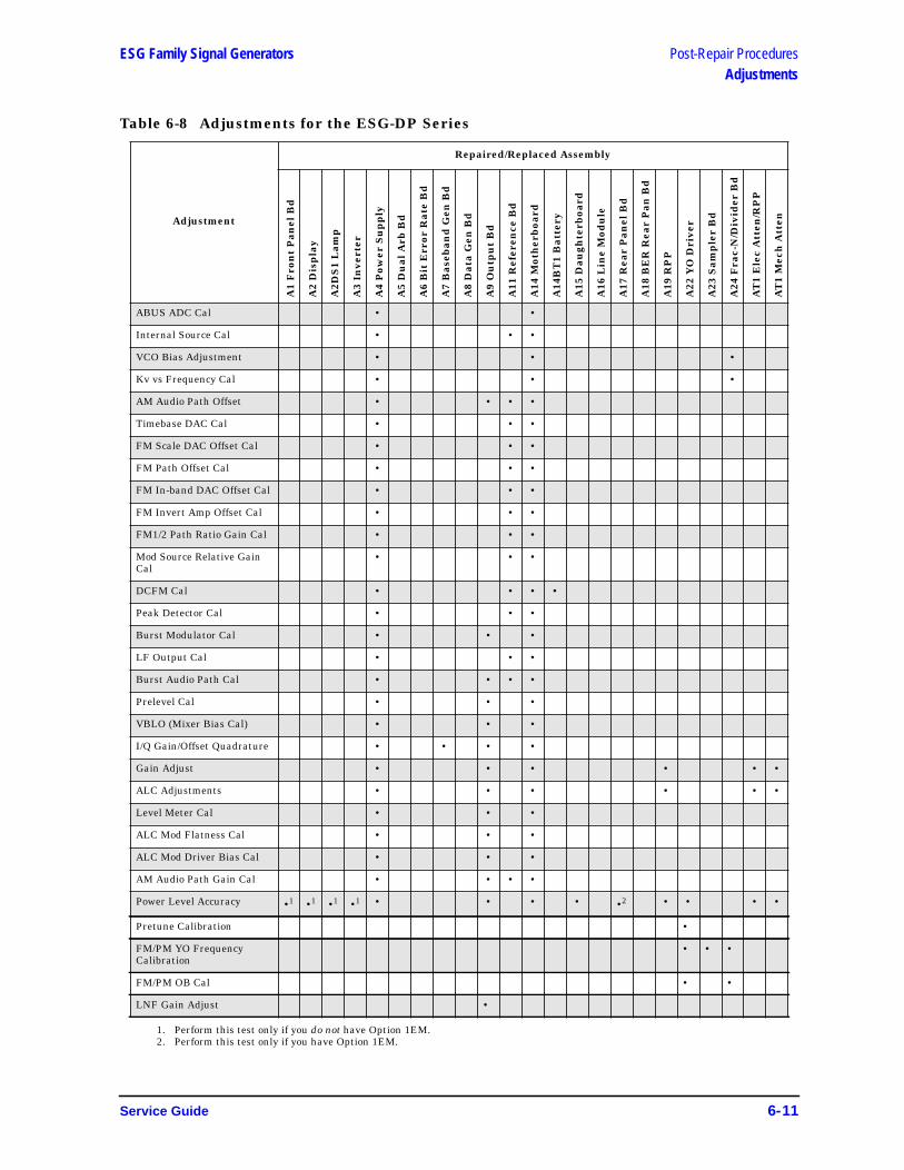
ESG Family Signal Generators Post-Repair ProceduresAdjustments
Table 6-8 Adjustments for the ESG-DP Series
Adjustment
Repaired/Replaced Assembly
A1
Fro
nt
Pan
el B
d
A2
Dis
pla
y
A2D
S1
Lam
p
A3
Inve
rter
A4
Pow
er S
up
ply
A5
Du
al A
rb B
d
A6
Bit
Err
or R
ate
Bd
A7
Bas
eban
d G
en B
d
A8
Dat
a G
en B
d
A9
Ou
tpu
t B
d
A11
Ref
eren
ce B
d
A14
Mot
her
boa
rd
A14
BT
1 B
atte
ry
A15
Dau
ghte
rboa
rd
A16
Lin
e M
odu
le
A17
Rea
r P
anel
Bd
A18
BE
R R
ear
Pan
Bd
A19
RP
P
A22
YO
Dri
ver
A23
Sam
ple
r B
d
A24
Fra
c-N
/Div
ider
Bd
AT
1 E
lec
Att
en/R
PP
AT
1 M
ech
Att
en
ABUS ADC Cal • •
Internal Source Cal • • •
VCO Bias Adjustment • • •
Kv vs Frequency Cal • • •
AM Audio Path Offset • • • •
Timebase DAC Cal • • •
FM Scale DAC Offset Cal • • •
FM Path Offset Cal • • •
FM In-band DAC Offset Cal • • •
FM Invert Amp Offset Cal • • •
FM1/2 Path Ratio Gain Cal • • •
Mod Source Relative GainCal
• • •
DCFM Cal • • • •
Peak Detector Cal • • •
Burst Modulator Cal • • •
LF Output Cal • • •
Burst Audio Path Cal • • • •
Prelevel Cal • • •
VBLO (Mixer Bias Cal) • • •
I/Q Gain/Offset Quadrature • • • •
Gain Adjust • • • • • •
ALC Adjustments • • • • • •
Level Meter Cal • • •
ALC Mod Flatness Cal • • •
ALC Mod Driver Bias Cal • • •
AM Audio Path Gain Cal • • • •
Power Level Accuracy •1 •1 •1 •1
1. Perform this test only if you do not have Option 1EM.
• • • • •2
2. Perform this test only if you have Option 1EM.
• • • •
Pretune Calibration •
FM/PM YO FrequencyCalibration
• • •
FM/PM OB Cal • •
LNF Gain Adjust •
Service Guide 6-11

ESG Family Signal Generators
7 Safety and Regulatory
This chapter provides information on the following:
• general safety information• lithium battery disposal• warranty and legal information
Service Guide 7-1
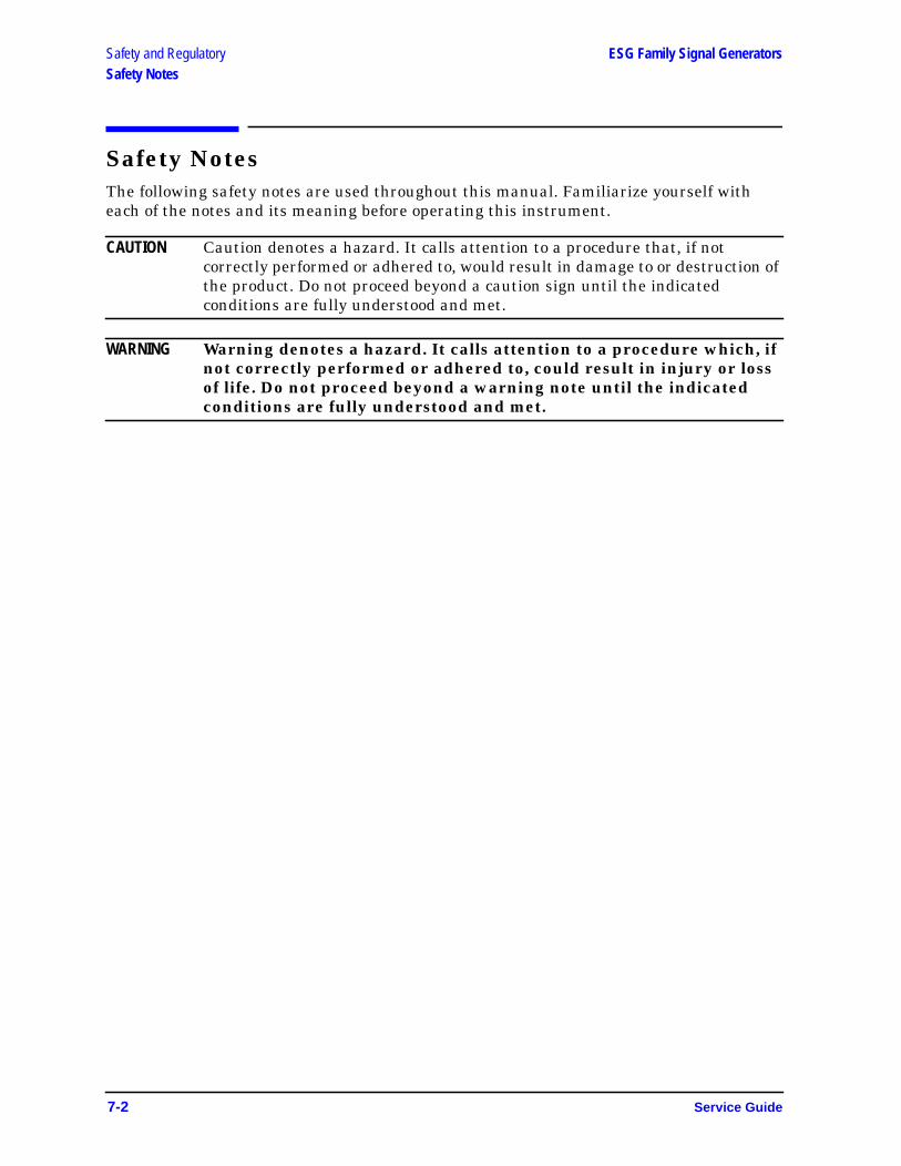
Safety and Regulatory ESG Family Signal GeneratorsSafety Notes
Safety NotesThe following safety notes are used throughout this manual. Familiarize yourself witheach of the notes and its meaning before operating this instrument.
CAUTION Caution denotes a hazard. It calls attention to a procedure that, if notcorrectly performed or adhered to, would result in damage to or destruction ofthe product. Do not proceed beyond a caution sign until the indicatedconditions are fully understood and met.
WARNING Warning denotes a hazard. It calls attention to a procedure which, ifnot correctly performed or adhered to, could result in injury or lossof life. Do not proceed beyond a warning note until the indicatedconditions are fully understood and met.
7-2 Service Guide

ESG Family Signal Generators Safety and RegulatoryGeneral Safety Considerations
General Safety ConsiderationsThe following safety notes apply specifically to ESG Family Signal Generators. These notesalso appear in other chapters of this service guide as required.
WARNING These servicing instructions are for use by qualified personal only.To avoid electrical shock, do not perform any servicing unless youare qualified to do so.
WARNING The opening of covers or removal of parts is likely to exposedangerous voltages. Disconnect the product from all voltage sourceswhile it is being opened.
WARNING The detachable power cord is the instrument disconnecting device.It disconnects the mains circuits from the mains supply before otherparts of the instrument. The front panel switch is only a standbyswitch and is not a LINE switch (disconnecting device).
WARNING The power cord is connected to internal capacitors that may remainlive for 5 seconds after disconnecting the plug from its power supply.
WARNING This is a Safety Class 1 Product (provided with a protective earthingground incorporated in the power cord). The mains plug shall onlybe inserted in a socket outlet provided with a protective earthcontact. Any interruption of the protective conductor inside oroutside of the product is likely to make the product dangerous.Intentional interruption is prohibited.
WARNING Danger of explosion if battery if incorrectly replaced. Replace onlywith the same or equivalent type recommended. Discard usedbatteries according to manufacturer’s instructions.
CAUTION Many of the assemblies in this instrument are very susceptible to damagefrom ESD (electrostatic discharge). Perform service procedures only at astatic-safe workstation and wear a grounding strap.
Service Guide 7-3

Safety and Regulatory ESG Family Signal GeneratorsLithium Battery Disposal
Lithium Battery DisposalWhen the battery on the A14 CPU/Motherboard is exhausted and/or ready for disposal,dispose of it according to your country’s requirements. You can return the battery to yournearest Agilent Technologies Sales and Service office for disposal, if required. (Refer toChapter 1, “Initial Troubleshooting and RF Block Diagrams,” for a list ofAgilent Technologies Sales and Service offices.)
7-4 Service Guide

ESG Family Signal Generators Safety and RegulatoryWarranty
WarrantyThis Agilent Technologies instrument product is warranted against defects in materialand workmanship for a period of three years from date of shipment. During the warrantyperiod, Agilent Technologies will, at its option, either repair or replace products whichprove to be defective.
For warranty service or repair, this product must be returned to a service facilitydesignated by Agilent Technologies. Buyer shall prepay shipping charges toAgilent Technologies and Agilent Technologies shall pay shipping charges to return theproduct to Buyer. However, Buyer shall pay all shipping charges, duties, and taxes forproducts returned to Agilent Technologies from another country.
Agilent Technologies warrants that its software and firmware designated byAgilent Technologies for use with an instrument will execute its programming instructionswhen properly installed on that instrument. Agilent Technologies does not warrant thatthe operation of the instrument, or software, or firmware will be uninterrupted orerror-free.
Limitation of Warranty
The foregoing warranty shall not apply to defects resulting from improper or inadequatemaintenance by Buyer, Buyer-supplied software or interfacing, unauthorized modificationor misuse, operation outside of the environmental specifications for the product, orimproper site preparation or maintenance.
NO OTHER WARRANTY IS EXPRESSED OR IMPLIED. AGILENT TECHNOLOGIESSPECIFICALLY DISCLAIMS THE IMPLIED WARRANTIES OF MERCHANTABILITYAND FITNESS FOR A PARTICULAR PURPOSE.
Exclusive Remedies
THE REMEDIES PROVIDED HEREIN ARE BUYER’S SOLE AND EXCLUSIVEREMEDIES. AGILENT TECHNOLOGIES SHALL NOT BE LIABLE FOR ANY DIRECT,INDIRECT, SPECIAL, INCIDENTAL, OR CONSEQUENTIAL DAMAGES, WHETHERBASED ON CONTRACT, TORT, OR ANY OTHER LEGAL THEORY.
Service Guide 7-5
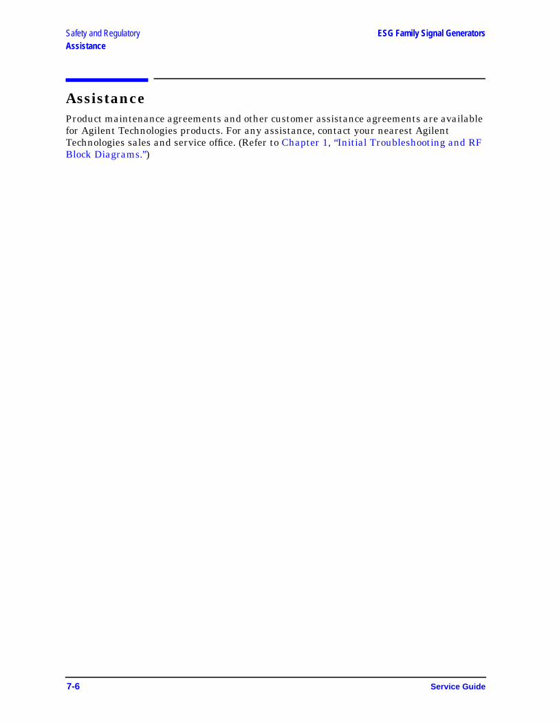
Safety and Regulatory ESG Family Signal GeneratorsAssistance
AssistanceProduct maintenance agreements and other customer assistance agreements are availablefor Agilent Technologies products. For any assistance, contact your nearest AgilentTechnologies sales and service office. (Refer to Chapter 1, “Initial Troubleshooting and RFBlock Diagrams.”)
7-6 Service Guide
ESG Family Signal Generators Safety and RegulatoryNotice
NoticeThe information contained in this document is subject to change without notice.
Agilent Technologies makes no warranty of any kind with regard to this material,including but not limited to, the implied warranties of merchantability and fitness for aparticular purpose. Agilent Technologies shall not be liable for errors contained herein orfor incidental or consequential damages in connection with the furnishing, performance, oruse of this material.
Service Guide 7-7
Safety and Regulatory ESG Family Signal GeneratorsCertification
CertificationAgilent Technologies Company certifies that this product met its published specificationsat the time of shipment from the factory. Agilent Technologies further certifies that itscalibration measurements are traceable to the United States National Institute ofStandards and Technology, to the extent allowed by the Institute’s calibration facility, andto the calibration facilities of other International Standards Organization members.
7-8 Service Guide

Index
AA1 front panel board
part number, 3-13, 4-11removal and replacement, 5-4
A11 referenceESG-A, -D
ABUS nodes, 2-29block diagram, 2-31
ESG-AP, -DPABUS nodes, 2-33block diagram, 2-35
part number, 3-12, 4-10removal and replacement, 5-56
A12 synthesizer/doublerABUS nodes, 2-37block diagram, 2-39part number, 3-12removal and replacement, 5-56
A14 CPU/motherboardABUS nodes, 2-41block diagram, 2-43, 2-45part number, 3-8, 3-10, 4-8removal and replacement, 5-18
A14BT1 batterypart number, 3-8, 3-10, 4-8removal and replacement, 5-24
A14Q501 transistorremoval and replacement, 5-26
A15 daughterboardpart number, 3-12, 4-10removal and replacement, 5-28
A16 line modulepart number, 3-14, 4-12removal and replacement, 5-32
A17 rear panel interfacepart number, 3-14, 4-12removal and replacement, 5-34
A18 BER rear panel interfacepart number, 3-14, 4-12removal and replacement, 5-34
A19 RPPblock diagram, 2-65part number, 3-8, 3-10, 4-8removal and replacement, 5-36
A2 displaypart number, 3-13, 4-11removal and replacement, 5-6
A20 downconvertorblock diagram, 2-47part number, 3-10removal and replacement, 5-39
A21 demodulatorblock diagram, 2-49part number, 3-10removal and replacement, 5-58
A22 YIG driverABUS nodes, 2-51block diagram, 2-53part number, 4-8removal and replacement, 5-40
A23 samplerABUS nodes, 2-55block diagram, 2-57part number, 4-10removal and replacement, 5-56
A24 frac-N/dividerABUS nodes, 2-59block diagram, 2-61part number, 4-10removal and replacement, 5-56
A25 pulse modulatorpart number, 3-8, 4-8removal and replacement, 5-41
A25 pulse modulator (w/ Option UNB)removal and replacement, 5-43
A2DS1 fluorescent lamppart number, 3-13, 4-11removal and replacement, 5-9
A3 inverterpart number, 3-13, 4-11removal and replacement, 5-10
A4 power supplypart number, 3-8, 3-10, 4-8removal and replacement, 5-12
A4 power supply (w/ Option 1EM)removal and replacement, 5-15
A5 dual arbitrary waveform generatorblock diagram, 2-5part number, 3-8, 3-10, 4-8removal and replacement, 5-58
A6 bit error rate testblock diagram, 2-7part number, 3-8, 3-10, 4-8removal and replacement, 5-58
A7 baseband generatorOptions UN3 UN4
block diagram, 2-9Options UN8 UN9, DBMIC
block diagram, 2-11part number, 3-8, 3-10, 4-8removal and replacement, 5-58
Index I-1

Index
A8 data generatorOptions UN3 UN4
block diagram, 2-13Options UN8 UN9, rev A & B
block diagram, 2-15Options UN8 UN9, rev C & D, flex
block diagram, 2-17part number, 3-8, 3-10, 4-8removal and replacement, 5-58
A9 outputESG-A
ABUS nodes, 2-19block diagram, 2-21
ESG-AP, -DPABUS nodes, 2-25
ESG-DABUS nodes, 2-23
ESG-D, -AP, -DPblock diagram, 2-27
part number, 3-12, 4-10removal and replacement, 5-56
abbreviations, 3-5, 4-5part descriptions, 3-5, 4-5
ABUS nodesA11 reference (ESG-A, -D), 2-29A11 reference (ESG-AP, -DP), 2-33A12 synthesizer/doubler, 2-37A14 CPU/motherboard, 2-41A22 YIG driver, 2-51A23 sampler, 2-55A24 frac-N/divider, 2-59A9 output (ESG-A), 2-19A9 output (ESG-AP, -DP), 2-25A9 output (ESG-D), 2-23
accessories, 3-74, 4-68adjustments, 6-7
ESG-A series, 6-8ESG-AP series, 6-10ESG-D series, 6-9ESG-DP series, 6-11
Agilent Technologiescontacting, 1-8
check the basics, 1-8review the warranty, 1-8
antistatic materials, 3-78, 4-72assemblies, 3-3, 4-3
defective, 3-4, 4-4part numbers, 3-7–3-14, 4-7–4-12rebuilt, 3-3, 4-3shipping, 3-4, 4-4
assembly replacementA1 front panel board, 5-4A11 reference, 5-56
assembly replacement (Continued)A12 synthesizer/doubler, 5-56A14 CPU/motherboard, 5-18A14BT1 battery, 5-24A14Q501 transistor, 5-26A15 daughterboard, 5-28A16 line module, 5-32A17 rear panel interface, 5-34A18 BER rear panel interface, 5-34A19 RPP, 5-36A2 display, 5-6A20 downconvertor, 5-39A21 demodulator, 5-58A22 YIG driver, 5-40A23 sampler, 5-56A24 frac-n/divider, 5-56A25 pulse modulator, 5-41A25 pulse modulator (w/ Option UNB), 5-43A2DS1 fluorescent lamp, 5-9A3 inverter, 5-10A4 power supply, 5-12A4 power supply (w/ Option 1EM), 5-15A5 dual arbitrary waveform generator, 5-58A6 bit error rate test, 5-58A7 baseband generator, 5-58A8 data generator, 5-58A9 output, 5-56AT1 electronic attenuator/RPP, 5-46AT1 mechanical attenuator, 5-48B1 small fan, 5-52B2 large fan, 5-54before replacing an assembly, 5-2daughterboard card cage boards, 5-56digital card cage boards, 5-58front panel, 5-60instrument cover, 5-64list of replaceable assemblies, 5-3post-repair procedures, 5-2rear panel (w/ Option 1EM), 5-70safety, 5-2semi-rigid cables, 5-73
assistance, 7-6AT1 electronic attenuator/RPP
part number, 3-8, 3-10, 4-8removal and replacement, 5-46
AT1 electronic attenuator/RPP block diagram, 2-63AT1 mechanical attenuator
part number, 3-8, 3-10, 4-8removal and replacement, 5-48
AT1 mechanical attenuator block diagram, 2-65
I-2 Index
Index
BB1 small fan
part number, 3-8, 3-10, 4-8removal and replacement, 5-52
B2 large fanpart number, 3-8, 3-10, 4-8removal and replacement, 5-54
batterydisposal of, 7-4
block diagramsA11 reference (ESG-A, -D), 2-31A11 reference (ESG-AP, -DP), 2-35A12 synthesizer/doubler, 2-39A14 CPU/motherboard, 2-43, 2-45A19 RPP, 2-65A20 downconvertor, 2-47A21 demodulator, 2-49A22 YIG driver, 2-53A23 sampler, 2-57A24 frac-N/divider, 2-61A5 dual arbitrary waveform generator, 2-5A6 bit error rate test, 2-7A7 baseband generator (Options UN3 UN4), 2-9A7 DBMIC baseband generator (Options UN8
UN9), 2-11A8 data generator - rev A & B (Options UN8 UN9),
2-15A8 data generator (Options UN3 UN4), 2-13A8 flex data generator - rev C & D (Options UN8
UN9), 2-17A9 output (ESG-A), 2-21A9 output (ESG-D, -AP, -DP), 2-27AT1 electronic attenuator/RPP, 2-63AT1 mechanical attenuator, 2-65ESG-A modulation and signal interconnects, 2-73ESG-A power supply and ground interconnects,
2-67ESG-A RF, 1-25ESG-A RF (Option 1E6), 1-25ESG-AP RF, 1-41ESG-AP RF (Option 1E6), 1-41ESG-D modulation and signal interconnects, 2-75,
2-77ESG-D power supply and ground interconnects,
2-69, 2-71ESG-D RF, 1-27ESG-D RF (Option 300), 1-39ESG-D RF (Option UN7), 1-33ESG-D RF (Option UN8 or UN9) Rev C or D, 1-31ESG-D RF (Option UND), 1-37ESG-D RF (Options UN3 UN4), 1-29ESG-D RF (Options UN8 UN9) Rev B, 1-35
block diagrams (Continued)ESG-DP RF, 1-43ESG-DP RF (Option UN7), 1-45ESG-DP RF (Option UND), 1-49ESG-DP RF (Options UN8 UN9), 1-47
blue repair tag, 1-51
Ccables, 3-15–3-44, 4-13–4-38calling Agilent Technologies, 1-8cautions
defined, 7-2list of, 7-3
certification, 7-8contacting Agilent Technologies, 1-8
calling, 1-8check the basics, 1-8packaging your signal generator, 1-10returning your signal generator, 1-10review the warranty, 1-8servicing your signal generator, 1-10
Ddaughterboard card cage boards
removal and replacement, 5-56defective assemblies, 3-3, 4-3digital card cage boards
removal and replacement, 5-58documentation, 3-75, 4-69
Eelectrostatic discharge
preventing, 7-3supplies, 3-78, 4-72
ESG-AP seriestroubleshooting, 1-23
ESG-DP seriestroubleshooting, 1-23
exchange assemblies, 3-3, 4-3
Ffront panel
removal and replacement, 5-60fuses, 1-12
Hhardware, 3-45–3-73, 4-39–4-67
Index I-3

Index
Iinitial troubleshooting, 1-1instrument cover
removal and replacement, 5-64
Llegal information, 7-1lithium battery, 7-4localized documentation, 3-76, 4-70
Mmodulation and signal interconnects
ESG-A series, 2-73ESG-D series, 2-75, 2-77
NNIST
United States National Institute of Standards andTechnology, 7-8
Ooptions, 1-3ordering parts, 3-2, 4-2
Ppackaging your signal generator, 1-10part descriptions
abbreviations, 3-5, 4-5performance tests, 6-2
ESG-A series, 6-3ESG-AP series, 6-5ESG-D series, 6-4ESG-DP series, 6-6
post-repair procedures, 6-1adjustments, 6-7performance tests, 6-2
power supply and ground interconnectsESG-A series, 2-67ESG-D series, 2-69, 2-71
Rrear panel (w/ Option 1EM)
removal and replacement, 5-70rebuilt assemblies, 3-3, 4-3repair tag, 1-51replaceable assemblies, 5-3replaceable parts, 3-78, 4-72
accessories, 3-74, 4-68cables, 3-15–3-44, 4-13–4-38documentation, 3-75, 4-69hardware and other, 3-45–3-73, 4-39–4-67kits, 3-78, 4-72localized documentation, 3-76, 4-70major assemblies, 3-7–3-14, 4-7–4-12miscellaneous, 3-74, 4-68ordering information, 3-2, 4-2
replacing fuses, 1-12retrofit kits, 3-78, 4-72returning your signal generator, 1-10
Ssafety and regulatory, 7-1safety considerations
list of warnings, 7-3sales and service offices, 3-2, 4-2semi-rigid cables
removal and replacement, 5-73service guide
using to troubleshoot, 1-2service offices, 3-2, 4-2service tag, 1-51servicing your signal generator, 1-10shipping, 3-4, 4-4
Ttroubleshooting, 1-1, 1-12, 1-21
assembly level, 2-1before you begin, 1-2, 2-2beginning, 1-12CPU functionality, 1-21CPU/motherboard LEDs, 1-15equipment required, 1-11error messages, 1-13ESG-AP series
additional information, 1-23ESG-DP series
additional information, 1-23front panel LEDs, 1-12functional check, 1-14initial, 1-1isolating the failed assembly, 1-19measuring voltage supplies, 1-16using assembly-level procedures, 2-2using this guide, 1-2
I-4 Index

Index
UUnited States National Institute of Standards and
Technology, 7-8
Wwarnings, 7-2, 7-3warranty information, 7-5
regarding this document, 7-7
Index I-5