advances in organic photovoltaics and methods for ...g3willia/documents/ece730_oscreview.pdf ·...
TRANSCRIPT

Advances in Organic Photovoltaics and Methods for
Effective Solar Cell Parameter Extraction
Graeme Williams*
Organic Optoelectronic Materials & Devices Laboratory
Electrical and Computer Engineering
University of Waterloo. Waterloo, ON Canada. N2L 3G1.
Correspondence should be addressed to [email protected]

1
Abstract. Alternative and renewable sources of energy have been identified as key areas of
research given our society’s projected energy demands. Photovoltaics are the most likely
candidate to meet the impending energy demands, with organic photovoltaics offering a
uniquely cheap route to achieve energy sustainability. The development of organic
photovoltaics (OPV) has been largely dictated by leaps of improvement in power conversion
efficiency (PCE) values, owing to significant advances in materials properties and device
architectures. These improvements have allowed for enhancement of PCE values from less
than 0.1% with simple organic films to a current value of 8.13% for bulk heterojunction devices.
This review will serve to examine the milestones of improvement in organic solar cells with a
particular emphasis on device architecture and the associated device physics. Accompanying
this discussion will be an overview of relevant device parameters and the current methods to
reliably extract these values from experimental data.

2
1. Introduction.
With worldwide energy usage expected to nearly double by the year 2050 and
worldwide oil reserves steadily depleting [1], research for alternative sources of energy has
become paramount. Even with more advanced oil extraction techniques, it is expected that
alternative, renewable sources of energy will be required by the end of the century. Given the
huge amount of solar radiation impingent on the earth, photovoltaics have been identified as
the most feasible candidate to meet the impending energy demands. Other approaches to
provide the required energy are either insufficient – such as wind, geothermal, hydroelectric
and tidal – or impractical – such as nuclear fission and fossil fuels in conjunction with carbon
sequestration [1].
Efficient photovoltaics began with single crystal silicon, which is frequently termed first
generation technology. These “p-i-n” solar cells generally achieve power conversion efficiency
values of ~15%-20% commercially, with experimental cells developed in lab environments
capable of 24-25% [2, 3]. Most recent advances are attributed to improvements in light in-
coupling by optimizing the silicon surface geometry. With further improvements, the first
generation of solar cells may reach their theoretical maximum efficiency of ~31%, defined as
the Shockley-Quessier limit [4]. This limit was calculated by taking into consideration all
insurmountable losses, especially due to energy losses from both low and high energy photons.
High energy photons produce hot carriers well above the band edges of the semiconductor,
which rapidly thermalize and thereby dissipate energy. In contrast, low energy photons below
the bandgap of silicon (~1.1eV) cannot promote an electron from the valence band to the
conduction band and are therefore lost as a source of energy.
From the above discussion, it is clear that single crystal silicon photovoltaics are
technologically limited by their fixed bandgap energy. They are further economically limited by
their high cost of production. In order to address these concerns, second and third generation
photovoltaics have been developed. Third generation photovoltaics are focused on the use of
nanocrystalline (quantum dot) materials that promise both reduced manufacturing costs and
improved efficiency beyond the Shockley-Quessier limit. In order to achieve high efficiency
values, third generation photovoltaics rely on hot carrier extraction and multiple generation
effects; however, neither phenomena have yet been successfully applied to nanocrystalline
solar cells in a practically relevant manner [5].
Second generation photovoltaics have lower efficiency values than first generation
photovoltaics and rely on decreased manufacturing costs to gain an economic advantage.
These are generally large area, thin film electronics and include vacuum-deposited amorphous
or polycrystalline semiconductors as well as solution-deposited organic semiconductors. By
removing the need for expensive physical or chemical vapour deposition, organic
semiconductors gain a significant competitive advantage. The use of thin film, amorphous

3
organic films also allows for the possibility of flexible substrates in combination with high
throughput reel-to-reel processing to further decrease costs. With most recent materials
allowing for 8.13% power conversion efficiencies [6], organic solar cells are becoming a strong
competitor in this particular generation of photovoltaics.
The structure of this review is as follows. Section 2 provides information on solar cell
fundamentals and notable device parameters, which will be used to describe the performance
of solar cells throughout this review. Section 3 serves to outline the history of organic
photovoltaics, with the goal of providing insight into the fundamental device physics and the
major challenges faced by this technology. Following this discussion, the device structure and
materials used in the most current organic solar cells will be examined with a focus on device
optimization and efficiency improvements. Section 4 will then focus on methods to reliably
extract relevant solar cell parameters from the basic solar cell output data. Such discussions
are especially relevant for the purpose of cross-comparisons among organic solar cells that can
vary not only in structure, but also in materials composition.
2. Background: Operation Principle and Notable Parameters.
A solar cell is fundamentally composed of one or several light-absorbing layers placed
between two electrodes, one of which must be transparent to allow for the passage of light.
The active layer(s) absorb(s) light to generate free carriers, which are then collected at the
electrodes. In an organic solar cell, the active layers are comprised of thin films of organic
semiconductors, which may be formed through either solution-based methods for polymeric
materials or through thermal evaporation for small-molecule materials.
This review article will focus on the polymeric, solution-deposited films, as these are
most relevant toward the goal of economically viable solar cells. However, it should be noted
that small molecule organic solar cells have also been successful in achieving high solar cell
efficiencies [7, 8], and have gained strong notoriety for their use in photodetectors. Since small
molecule films are vacuum deposited, multiple (>2) heterojunction devices have been shown to
be feasible, allowing for strong gains in device quantum efficiency. The reader is strongly
encouraged to examine reference [9] for a very thorough review by Forrest and coworkers on
the subject of small molecule solar cells and photodiodes. A more recent review on the current
status of small molecule organic solar cells is provided in [10].
In contrast to the conduction and valence bands with inorganic semiconductors, organic
semiconductors are generally discussed in terms of the analogous quantities known as the
lowest unoccupied molecular orbital (LUMO) and highest occupied molecular orbital (HOMO).
Common organic solar cells make use of either plastic or glass substrates, with a tin-doped
indium oxide (ITO) bottom electrode and a low work function metal top electrode (most

4
commonly calcium, magnesium or aluminum). This common configuration is shown in Figure 1
A) and B).
Figure 1 - A) Common structure of a simple, single-layer organic solar cell with B) associated energy diagrams of separated
components. ITO, Al, , IP and Eg refer to the ITO work function, aluminum work function, and semiconductor electron affinity, ionization potential and bandgap respectively (Images adapted from ref [11]). C) Equivalent circuit model for an
organic solar cell. The solar cell is fundamentally composed of a current source and a rectifying component, modelled as a diode. Rs and Rsh refer to series and shunt resistances respectively, which occur due to non-idealities within the solar cell.
In the simple illustration in Figure 1A) and B), a photon enters the device through the
transparent electrode to generate an exciton within the organic semiconductor. The exciton is
further broken down into an electron and a hole, which are collected at the aluminum and ITO
electrodes respectively. It is important to note that these energy diagrams are only drawn for
the isolated components and do not include band bending due to Fermi level alignment. The
basis for preferential breaking of the exciton is discussed in greater detail in Section 3.
Given the above discussion, an organic solar cell under light exposure may be best
understood as a current source. Due to the nature of exciton dissociation and carrier
collection, as will be discussed in Section 3, the organic solar cell is also a rectifying device.
Additional resistances, Rseries and Rshunt may also be considered due to several non-idealities and
inefficiencies in the device structure and operation. Rseries occurs due to the contact resistances
between the electrodes and the organic semiconductor, in addition to the resistances of the
bulk semiconductor and the electrodes themselves. Rshunt is included due to leakage and
recombination current within the device. A final equivalent circuit model of the organic solar
cell is shown in Figure 1 C).
Simple comparisons among solar cells are usually made in terms of their power
conversion efficiencies (PCE or PCE), which refer to the amount of useful electrical energy
produced as a function of the input optical power. PCEs are typically reported in terms of a
standard one-sun (100mW/cm2), air mass 1.5 (AM1.5) exposure produced by a solar simulator.
This spectrum is analogous to light impingent to the earth after it has traveled through the
earth’s atmosphere a distance of 1.5 atmosphere thicknesses. A number of other notable solar
cell parameters include:
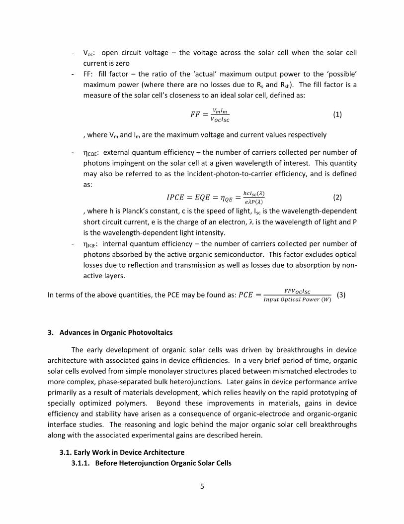
- Isc: short circuit current – the solar cell current when the voltage across the solar cell
is zero
5
- Voc: open circuit voltage – the voltage across the solar cell when the solar cell
current is zero
- FF: fill factor – the ratio of the ‘actual’ maximum output power to the ‘possible’
maximum power (where there are no losses due to Rs and Rsh). The fill factor is a
measure of the solar cell’s closeness to an ideal solar cell, defined as:
(1)
, where Vm and Im are the maximum voltage and current values respectively
- EQE: external quantum efficiency – the number of carriers collected per number of
photons impingent on the solar cell at a given wavelength of interest. This quantity
may also be referred to as the incident-photon-to-carrier efficiency, and is defined
as:
(2)
, where h is Planck’s constant, c is the speed of light, Isc is the wavelength-dependent
short circuit current, e is the charge of an electron, is the wavelength of light and P
is the wavelength-dependent light intensity.
- IQE: internal quantum efficiency – the number of carriers collected per number of
photons absorbed by the active organic semiconductor. This factor excludes optical
losses due to reflection and transmission as well as losses due to absorption by non-
active layers.
In terms of the above quantities, the PCE may be found as:
(3)
3. Advances in Organic Photovoltaics
The early development of organic solar cells was driven by breakthroughs in device
architecture with associated gains in device efficiencies. In a very brief period of time, organic
solar cells evolved from simple monolayer structures placed between mismatched electrodes to
more complex, phase-separated bulk heterojunctions. Later gains in device performance arrive
primarily as a result of materials development, which relies heavily on the rapid prototyping of
specially optimized polymers. Beyond these improvements in materials, gains in device
efficiency and stability have arisen as a consequence of organic-electrode and organic-organic
interface studies. The reasoning and logic behind the major organic solar cell breakthroughs
along with the associated experimental gains are described herein.
3.1. Early Work in Device Architecture
3.1.1. Before Heterojunction Organic Solar Cells

6
The simplest form of an organic solar cell comprises a single homogenous organic
semiconductor placed between a transparent conductive oxide (TCO) bottom electrode and a
metallic top electrode. Some of the earliest work on this device architecture can be traced back
to simple films of chlorophyll-a electrodeposited between two metal electrode in 1975 [12]. In
both this work and much later work at Xerox in 1993 [13], it was shown that organic
semiconductors have sufficient conductivity and hole carrier densities to form p-type Schottky
barrier contacts with adjacent metal layers. In the latter work, the synthesized polymer poly(p-
phenylene vinylene) (PPV) was used as the organic layer, although it is noted that polyacetylene
and polythiophenes had been previously examined for similar purposes [11].
Riess et. al., Antoniadis et. al. and Marks et. al. further showed that favourable
HOMO/LUMO bending at aluminum-PPV Schottky contacts could be used for photovoltaic
applications in 1994 [14-16]. The energy diagram for this system is provided in Figure 2 A).
Upon absorption of a photon, an exciton is formed in the PPV semiconductor. The exciton is
dissociated into its constituent electron and hole due to the electric field at the Schottky
contact. Electrons may be collected directly at the aluminum electrode, whereas holes must
diffuse along the thickness to the semiconductor to be collected at the ITO electrode.
Figure 2 - A) Energy diagram for a simple PPV-Al Schottky solar cell. B) IV output characteristic for a representative PPV-Al Schottky solar cell. Note that the fill factor is rather poor (~0.2) and the current density is very low for solar cells made with
this device structure. (Figures adapted from [14])
Each of these early studies identify similar open circuit voltages of ~1.2V, rather poor
short circuit current values at 1-2 A/cm2 and power conversion efficiency values near ~0.1-1%
for low light conditions [14, 15]. A representative IV output characteristic for this system is
provided in Figure 2 B). Antoniadis et. al. note that further increasing the light source power
results in smaller gains in photocurrent, thereby reducing the device efficiency. Although it is
not directly reported, this effect is very likely due to a reduction in the device quantum
efficiency as a consequence of bimolecular recombination. In this case, photogenerated
electrons and holes interact and recombine either radiatively or non-radiatively. As such, an
increase in photogenerated carrier density results in greater levels of recombination.
This simplistic structure is clearly limited in its capacity for photovoltaics, as proven by
its underwhelming solar cell properties,. Excitons are dissociated primarily at the depletion
layer formed at the Schottky contact. Since the exciton diffusion length is typically below 20nm

7
for organic materials [17], only a very small number of excitons generated very close to the
Schottky contact contribute to harvestable carriers and photocurrent. The active organic layer
must be thick, however, or it will not efficiently absorb light due to significant transmittance
losses.
3.2. Planar Heterojunction Organic Solar Cells
In order to address the poor device behaviour and losses associated with single layer
organic solar cells, researchers sought device structures that encouraged exciton dissociation.
Such an approach had already been applied with thermally evaporated small molecules since
1986 by Tang from Kodak [18]. In this work, Tang used a copper pthalocyanine (CuPC)-perylene
tetracarboxylic planar junction to achieve power conversion efficiencies of 0.95% with fill
factors as high as 0.65.
In the early work by Tang, it was shown that the offset in HOMO/LUMO of the two
organic semiconductors allowed the heterojunction to act as an efficient interface for exciton
dissociation. The material with higher electron affinity is denoted as the acceptor, whereas the
material with lower electron affinity is denoted as the donor. Under exposure to light, a
photogenerated exciton formed on a donor molecule may diffuse to the heterojunction, where
its electron can rapidly transfer to an acceptor molecule. This transfer is favourable as long as
the LUMO offset between the donor and acceptor is larger than the Coulombic stabilization
energy of the exciton. More recent work has also shown probable dipole formation at the
donor-acceptor interface, which further helps to separate electron-hole pairs and also hinders
geminate recombination [19].
Upon exciton dissociation, the free carriers may then diffuse to their corresponding
electrodes where they are collected to generate photocurrent. This process is shown in Figure
3. In contrast to the single layer device, which must support bipolar transport, a heterojunction
device allows for electron transport along the high electron affinity material and hole transport
along the low ionization potential material. This scheme significantly reduces bimolecular
recombination and thereby increases photocurrent. As an additional benefit, since the
heterojunction is present in the bulk of the film, the number of excitons within diffusion length
of the junction increases substantially compared to the simple Schottky solar cell.

8
Figure 3 - Energy diagram of the HOMO/LUMO offset for a planar heterojunction organic solar cell. The energy levels are drawn for individual, separate components to show the general device behaviour. Contact between the organic layers and the electrodes may lead to some HOMO/LUMO bending, which has not been shown here. (Figure adapted from ref [11]).
The difficulty of incorporating a planar heterojunction in polymeric solar cells arises
from solution-coating a top polymer layer without re-dissolving the underlying polymer layer.
Methods to accomplish this task generally include making use of orthogonal solvents, which
dissolve one polymer but not the other, or through the use of polymer precursors, where an
insoluble polymer film is formed directly on the substrate. Later work in 1999 and 2000
showed these approaches to be feasible [20, 21], although by then much of the research had
shifted to bulk heterojunction solar cells, which are described further in Section 3.3.
As a consequence, much of the early work in planar heterojunctions involved purely
small molecule films, as discussed in Forrest and coworkers’ review [9]. Other groups combined
polymers and small molecules into solar cells by spincoating a bottom polymeric layer and
subliming a strong acceptor layer on top, including perylene derivatives [22, 23] and fullerene
(C60) [24-28]. While these devices are inherently expensive, as they require a multi-step
fabrication process involving both solution- and vacuum-deposition of organic materials, they
served as an important milestone for efficiency. These devices also provided insight into
organic solar cell device behaviour and architecture and, as such, are described briefly below.
The use of C60 in organic photovoltaics arose as a consequence of their proven
quenching of organic excited states. In this early work, Sariciftci et. al. prepared thin films of
poly[2-methoxy,5-(2'-ethyl-hexyloxy)-p-phenylene vinylene] (MEH-PPV) sensitized with small
concentrations of C60 [29]. The researchers witnessed near complete loss of
photoluminescence and a decrease in luminescence decay time in the composite compared to
a pure MEH-PPV film, indicative of fast (~ps) electron transfer from MEH-PPV to C60. The
absence of new absorption spectral features further showed that no such transfer occurs at the
ground state. This work was simultaneously completed by Morita et. al. for a different
polymer, showing that the significant quenching of photoluminescence intensity could be
achieved at C60 concentrations as low as 1% [30]. Later work by Lee et. al. demonstrated this
effect for a different polymer, and also described an associated enhancement in
photoconductivity for the composite polymer:C60 films. This gain in photoconductivity was
attributed to extended free carrier lifetime arising from decreased radiative recombination
[31].

9
Sariciftci et. al. were the first to examine polymer-C60 heterojunctions in 1993 with an
ITO/MEH-PPV/C60/Au structure [27, 28]. This device showed some improvement in fill factor to
0.48, but it exhibited poor power conversion efficiencies of ~0.04% when exposed to light with
1mW/cm2 intensity. The device also exhibited significantly lower dark current than its single-
layer predecessor and showed a linear current dependence on light intensity. These results
prove that the device structure is successful in inhibiting bipolar transport across individual
layers, thus limiting bimolecular recombination. These were results were confirmed by Morita
et. al. with a thiophene-based polymer-C60 heterojunction showing good device rectification
and measurable photocurrent [25].
These simple planar heterojunctions showed very modest improvements in external
quantum efficiency with optimization of device fabrication [23, 24]. The underwhelming device
performances highlight a fundamental problem with the planar heterojunction structure: most
of the photogenerated excitons are not within their diffusion length of the heterojunction. This
fact was emphasized in a study by Roman et. al., who calculated the point of maximum optical
electric field of monochromatic light within a simple polymer-C60 planar heterojunction [26].
This research showed that by designing the device such that the maximum electric field was
centred on the heterojunction, it was feasible to substantially increase the quantum efficiency
of the device. This improvement is due to the increase in the number of excitons generated
very near heterojunction, where free carriers may be generated.
As a point of interest, in 1998, Friend and coworkers showed some success with planar
heterojunction films composed of a polythiophene donor and a cyano-based derivative of MEH-
PPV as an acceptor [32]. In contrast to the above work, the acceptor film was doped with ~5%
of the donor species and, similarly, the donor film was doped with ~5% of the acceptor species.
This work was further unique in that the donor/acceptor films were formed on two different
substrates and a lamination method was used to couple the device together. This fabrication
approach is incredibly attractive, as the metal-coated substrates can be pre-prepared very
cheaply and the active layers only require simple solution-based processing. Using this
approach, the authors were able to achieve more reasonable PCE values of 1.9% under
77mW/cm2, AM1.5 exposure conditions. This notion of laminate-processing of solar cells was
revisited much later in 2008 by Yang and coworkers [33].
3.3. Bulk Heterojunction Organic Solar Cells
The bulk heterojunction concept was introduced as an answer to the poor efficiencies
that arise due to excitons being generated too far from the planar heterojunction. In a bulk
heterojunction, the donor and acceptor species are blended together in a common solvent and
deposited simultaneously, as shown in Figure 4 A). By blending the two species together, one
may ensure that photogenerated excitons will always be within their diffusion length of a
heterojunction. As such, one can minimize recombination of the photogenerated excitons. It is

10
also worth noting that, while both electrodes are in direct contact with both the donor and
acceptor materials in a bulk heterojunction, electrode work function mismatch allows for a
sufficiently large internal electric field to collect separated carriers at the proper electrodes.
This is shown in the simplified energy diagram in Figure 4 B), which illustrates a bulk
heterojunction device under short-circuit conditions.
If the blend is defined properly, both the donor and acceptor may percolate across the
electrodes, allowing for a blended film that exhibits bicontinuous phases. The interpenetrating
network allows for efficient free carrier motion across the active layer of the device, as the
holes may remain in the donor phase and the electrons may remain in the acceptor phase. This
bicontinuous distribution of materials occurs naturally with polymer/polymer and
polymer/small molecule mixtures deposited from solution due to the low entropy of mixing of
macromolecules. By evaporating the solvent during deposition in a controlled manner, it is
feasible to ‘freeze’ the device in this bicontinuous phase configuration.
Figure 4 - A) Illustration of a bulk heterojunction placed between ITO and Al electrodes. Note that the donor (red) and acceptor species (blue) are well dispersed throughout the active layer and show discrete phases. B) Simplified energy
diagram of the same. Interfacial band bending and associated effects have been ignored for simplicity. Also note that the LUMO and HOMO levels are shown as continuous across the entire film, which is not necessarily true unless the film shows
ideal mixing. (Images adapted from ref [11] and ref [34]).
Following the success of C60 when used as an electron accepting species, Yu et. al.
formed simple ITO/MEH-PPV:C60/Ca bulk heterojunction devices in 1994 for use as
photodetectors [35]. The inclusion of ~10% C60 by weight improved the photocurrent response
of the photodiode by nearly an order of magnitude. Unfortunately, the weight ratio of C60 in
the film is fundamentally limited by the poor solubility of C60. It is therefore unrealistic to
assume proper C60 phase distribution and separation within the organic film. In order to
enhance the solubility of C60, Hummelen et. al. examined fulleroid and methanofullerene
derivatives that offer enhanced solubility due to bulky side-groups which inhibit fullerene
aggregation [36]. In this work, the researchers developed phenyl-C61-butyric acid methyl ester
(PCBM), which shows high solubility in most common organic solvents.
In 1995, Yu et. al. continued their earlier work from [35], replacing C60 with PCBM to
form bulk heterojunction devices with higher acceptor concentrations [37]. The authors
successfully increased the amount of PCBM to a weight ratio of 4:1 PCBM:MEH-PPV, such that
roughly every repeat unit on the polymer would have a corresponding fullerene acceptor.

11
Devices made using an ITO/MEH-PPV:PCBM/Ca structure were capable of achieving Isc, Voc,
peak EQE and PCE values of 2mA/cm2, 0.82V, 29% and 2.9% respectively when exposed to
20mW/cm2 monochromatic (430nm) light. The power conversion efficiency reported in [37] is
a substantial improvement over previous single layer organic solar cells and serves as a
milestone in organic photovoltaics. These devices also showed a nearly linear dependence of
photocurrent on light intensity, further emphasizing that the bulk heterojunction structure
inhibits bimolecular recombination.
In the same year, both Yu et. al. and Halls et. al. developed bulk heterojunction solar
cells based on mixed donor/acceptor polymers [38, 39]. In both cases, the researchers made
use of MEH-PPV as the donor and CN-PPV as the acceptor since CN-PPV has a higher electron
affinity and a lower ionization potential. Fast electron transfer from MEH-PPV to CN-PPV was
first shown via steady state photoluminescence measurements, where the photoluminescence
intensity dropped considerably for mixing ratios between 1:4 and 4:1 CN-PPV:MEH:PPV by
weight. Both groups obtained similar peak EQE values of 5-6%, with Yu et. al. reporting PCE
values on the order of 0.9% when illuminated under low intensity, monochromatic light.
In both [37, 38], Yu et. al. noted that the open circuit voltage decreased from ~1.3-1.6V
for a single layer MEH-PPV device to ~1V and ~0.8V for the MEH-PPV:CN-PPV and MEH-
PPV:PCBM bulk heterojunction devices respectively. The authors note that the same reduction
in open circuit voltage occurs with pure, single layer CN-PPV devices. While the origin of this
variation has been subject to some debate, recent results and discussions from Crispin et. al.
and Braun et. al. strongly suggest this work function lowering is due to a Fermi level pinning
effect at the electrode-organic interface [40, 41].
In brief, one may describe single layer MEH-PPV solar cell devices as thin-film diodes
based on a fully depleted Schottky diode scheme [38]. This conclusion has been made from
two significant pieces of information:
- Voc is dictated only by the work function difference between the electrodes
- Single layer devices exhibit constant capacitance across the device for voltages
below Voc, implying that the polymeric layer is already fully depleted
This simple MEH-PPV-based device behaviour arises because the HOMO is lower than the Fermi
level of ITO and the LUMO is higher than the Fermi level of Ca. However, since CN-PPV and
PCBM have electron affinities greater than the work function of Ca, solar cells making use of
these materials show an altered (lowered) open circuit voltage due to Fermi level pinning.
Additional lowering of the Voc may be due to device non-idealities, relating to poor fill factors
caused by high series resistances and low shunt resistances. The topic of open circuit voltage is
discussed in greater detail in Section 3.4.2.
3.4. Enhancement and Optimization of Modern Organic Solar Cells

12
Much of the groundwork for modern organic photovoltaics was set with the
development of the bulk heterojunction and with the realization of PCBM as an acceptor
material. Following the initial successes described above, there was a huge surge of research
interest in organic photovoltaics. The remainder of this review will therefore focus on the most
prominent and successful class of organic solar cells, which were based off of the nascent
results described above: fullerene/PCBM-based bulk heterojunctions.
As a point of note, very interesting work has also been completed on the development
of block copolymers, where a single polymer chain comprises of both donor and acceptor
groups [42-45]. In such a system, the differing blocks tend to phase separate, which is ideal for
application in bulk heterojunctions. Unfortunately, these cells generally exhibit poorer
performance than simple mixed-polymer systems, with very recent work in 2009 only showing
0.49% PCE [46]. Readers interested in these developments are referred to [42], where Sun
discusses the fundamental requirements for acceptor-donor block copolymers.
3.4.1. Improvement in Device Efficiencies through Advances with the Donor Material
Bulk Heterojunction Solar Cells with PPV-Based Donor Materials
In the early work on organic photovoltaics, researchers made use of PPV and PPV-
derivative polymers as the primary absorbing and donor species in heterojunction cells [27, 28,
37]. In 2001, Shaheen et. al. developed bulk heterojunctions of poly[2-methyl,5-(3*,7**
dimethyloctyloxy)]-p-phenylene vinylene) (MDMO-PPV) with PCBM to produce solar cells with
2.5% PCE, the highest reported efficiencies for polymeric solar cells at the time [47]. Much of
the improvement witnessed in this particular experiment can be attributed to two experimental
considerations:
- The use of chlorobenzene (CB) instead of toluene as a solvent for spincoating
allowed for much smoother films, owing to better polymer mixing and polymer
phase distribution.
- The high concentration of PCBM in the composite allowed for a larger number of
PCBM percolation pathways and also granted better mobility for both electrons and
holes within the film.
The first experimental consideration highlights the importance of film morphology for
bulk heterojunctions, which remains a concern in all bulk heterojunction organic photovoltaics
regardless of the chosen donor species. In their 2007 review, Günes et. al. listed a number of
factors that may affect the characteristics of the solution-deposited film, including: the solvent,
the processing temperature, the ratio of the donor to acceptor, the concentration and the
chemical structure of the chemical species [48]. Beyond these factors, the method of
depositing the film (spincasting, dropcasting, doctor blading, etc.), the cleanliness of the

13
deposition environment (typically a nitrogen glovebox) and the time between solution
preparation and deposition can all have significant effects on film quality and morphology.
The second experimental consideration further stresses the importance of film
morphology, but also notes the anomalous increase in hole mobility when MDMO-PPV is
incorporated into a blend structure with PCBM. Melzer et. al. found that the hole mobility in a
20:80% MDMO-PPV:PCBM film was only an order of magnitude lower than the electron
mobility in a pure PCBM film [49, 50]. This is in contrast to the pure MDMO-PPV film, where
the hole mobility is four orders of magnitude smaller than the pure PCBM film electron
mobility. This phenomenon is counterintuitive; increasing the PCBM concentration dilutes the
MDMO-PPV concentration and should decrease the number of conductive pathways for hole
transport. While the cause of this phenomenon has not yet been identified, it has been
suggested that the improvements arise from a change in the configuration of the PPV-based
polymers, which allows for better stacking and therefore grants higher carrier mobility.
Despite the impressive initial 2.5% PCE shown by Shaheen et. al. [47], further
improvement in PPV-PCBM-based bulk heterojunctions only allowed for modest increases in
PCE values of 3 to 3.3% [51-53]. Even with the anomalous increase in hole mobility noted
above, the mobility and associated conductivity of PPV polymers are still quite low.
Furthermore, the wide bandgap of PPV polymers prohibits the absorption of low energy
photons and thereby restricts the maximum photocurrent. For this reason, researchers began
examining small bandgap polymers and polymers with higher hole mobilities. As a point of
note, hole mobility is typically inversely related to ionization potential for organic materials.
Given similar bandgap energies and film forming capabilities, a high hole mobility material
should then exhibit a larger HOMO/LUMO offset with PCBM, as shown with poly-
3(hexylthiophene) (P3HT) in Figure 5 A).
Figure 5 - A) Illustration of the difference in HOMO/LUMO and bandgap for P3HT vs. MEH-PPV donor polymers when used in bulk heterojunction organic solar cells with PCBM. (Figure adapted from ref [54]). B) EQE curves at two active layer
thicknesses for the preliminary P3HT:PCBM devices discussed in ref [55]. (Figure adapted from ref [55]).
Bulk Heterojunction Solar Cells with P3HT Donor Materials
For much of the past decade, P3HT:PCBM bulk heterojunctions have been the focus for
organic solar cells. The shift to P3HT as a donor species began with promising results in 2002
from Schilinsky et. al., who showed that ITO/PEDOT:PSS/P3HT:PCBM/Ca devices could achieve

14
very high EQE values, as shown in Figure 5 B) [55]. In this work, they also showed an increase in
short circuit current with increasing temperature, as well as the capacity for the system to
achieve an IQE near 100% at the peak absorption wavelength of ~550nm.
Post-processing techniques later allowed for increases in P3HT:PCBM-based PCE values
to 3.5% [56]. In this work, the researchers heated the as-fabricated device (with the same
structure as [55], except with an LiF/Al top electrode) above the glass transition temperature of
P3HT while simultaneously applying an electrical bias to the device. Increasing the temperature
of the polymer beyond its glass transition temperature allowed the P3HT:PCBM polymer
mixture to reorganize itself and phase separate more effectively than in the initial casting of the
film. The authors suggest that the electrical bias applied to the film further encouraged the
polymer to orient itself in such a manner to allow for efficient charge transport.
Significant work has been dedicated to the optimization of process conditions for
P3HT:PCBM bulk heterojunctions in much the same manner as was discussed for PPV:PCBM
solar cells. The reader is encouraged to examine [57] and [58] by Brabec and coworkers for
tabulated data on this topic. In general, researchers have sought to optimize the percolation,
structure and orientation of both the donor and acceptor materials in the film through
variations in materials properties, deposition conditions and post-processing treatments [59-
74]. A detailed analysis of the major conclusions regarding optimization of P3HT within the
P3HT:PCBM active layer in bulk heterojunction devices is provided below. While these
optimizations have been made for P3HT:PCBM heterojunctions, much of these considerations
can and should be extended to future donor materials. This sum of knowledge has allowed for
reasonable levels of reproducibility in device fabrication among different groups, with reported
PCE values on the order of 4-5% [63, 65, 66, 71, 75].
The highest efficiencies for P3HT:PCBM bulk heterojunction solar cells are obtained at
active layer compositions of 0.8-1:1 P3HT:PCBM by weight [59, 61, 63, 66]. At these
concentrations, the P3HT:PCBM film exhibits balanced electron and hole transport and is less
susceptible to space-charge limited carrier transport. Furthermore, this balanced concentration
allows for percolation of both PCBM and P3HT within the bulk heterojunction and across the
length of the device. This is a much lower ‘ideal’ PCBM concentration compared to PPV:PCBM-
based solar cells. One reason for this variation is that P3HT films have higher ‘pure’ hole
mobilities and P3HT:PCBM films therefore do not benefit from the same anomalous hole
mobility improvements as described above for PPV:PCBM-based devices. As an additional
factor, at very high PCBM concentrations, thermal annealing of the P3HT:PCBM film leads to
the formation of large PCBM crystallites that cause film cracking and drastically increase the
organic-metal electrode contact resistance [59, 67].
Following the results from [56], thermal annealing of P3HT:PCBM bulk heterojunction
devices was found to result in improved EQE, short circuit current, fill factor and device PCE

15
values [62-66, 69], as shown in Figure 6 A). This has been attributed to better phase separation
of the polymers and due to the formation of both PCBM nanocrystallites and larger P3HT
crystallites, allowing for high carrier mobilities [65, 67, 69, 74]. For the same reasons, slow
drying or “solvent annealing” of the P3HT:PCBM film allows for higher device efficiencies [61,
63, 72, 73], as shown in Figure 6 B). To prove this effect, Li et. al. showed that the optical
absorption of a thick, slowly dried film was the same pre- and post-anneal. In contrast, a
quickly dried film developed the characteristic crystalline P3HT peaks only after annealing,
indicating poor initial film morphology [63], as shown in Figure 6 C). Furthermore, the slowly
dried sample exhibits a strongly red-shifted absorption curve, which implies a higher degree of
molecular - interaction (granting higher hole mobility) due to structural ordering. The
solvent annealing approach may be pertinent for very low temperature manufacturing
processes for highly flexible substrates or for newly developed donor polymers that are
unstable at elevated temperatures.
Figure 6 - A) IV output characteristics for P3HT:PCBM bulk heterojunction solar cells that have undergone thermal annealing. Devices 1-4 correspond to devices with 0min, 10min, 20min and 30min treatment at 110
oC, performed prior to top electrode
deposition. The active layer in all devices was 210nm and the film was dried slowly for 20 minutes prior to thermal annealing. B) IV output characteristics for P3HT:PCBM bulk heterojunction solar cells with different active layer drying times.
Devices 5-8 correspond to drying times of 20 minutes, 3minutes, 40 seconds and 20 seconds respectively. C) Absorption of P3HT:PCBM active layers with varying dry times, as cast and annealed. (Figures adapted from ref [63])
Some additional useful knowledge gleaned from the numerous P3HT:PCBM bulk
heterojunction solar cell optimization experiments include:
- Annealing the P3HT:PCBM film after top electrode deposition (on a completed
device) provides better efficiencies than annealing the sample prior to top electrode
deposition [64, 65]. This has been attributed to enhanced interfacial chemical
bonding and potential metal diffusion during the annealing process, which may
allow for decreased interfacial carrier recombination and a larger contact area to
reduce contact resistance.
- Increasing the device temperature during testing increases the short circuit current.
The authors attribute this due to reduced trap-induced carrier recombination. In
this regard, the thermal energy kBT is greater than the energy of the trap state, so
rapid de-trapping occurs and trap-induced recombination is minimized [60].
- Thicker P3HT:PCBM films minimize pinholes and cracking, thereby reducing leakage
current and increasing shunt resistance [63].
16
- P3HT:PCBM films spun from dichlorobenzene (DCB) lead to devices with better as-
spun efficiencies; however, these films generally require higher temperature
annealing [62]. This variation is due to the lower volatility of DCB compared to CB,
which leads to a longer film drying time and thereby increases the as-spun
efficiencies for the same reasons discussed above and noted in [63].
- The addition of a non-solvent can be used to control P3HT aggregation in solution
and therefore control the formation of P3HT crystallites within a cast film [75]. This
method has been successfully applied to produce as-cast samples with ~4% power
conversion efficiency. Similar to solvent annealing, the absence of a heat-treatment
in this non-solvent approach may be useful for very low temperature manufacturing
processes and for future temperature-sensitive polymers.
Schilinsky et. al. also found that a large P3HT molecular weight (MW), greater than 10
kDa, is required for high efficiency P3HT:PCBM bulk heterojunction solar cells [68]. The authors
note that MW is directly related to intermolecular - interactions and to the formation of
P3HT crystallites, as observed by the absence of the characteristic crystalline P3HT absorption
peaks in small MW P3HT samples. This was further evidenced by the fact that high MW P3HT
samples generally yield films with higher measured hole mobilities.
It was later found that the annealing treatment must be fine-tuned to different MW
polymers, with larger MW P3HT requiring higher anneal temperatures and longer anneal times
[70]. This variation is related to the stronger degree of aggregation for large MW P3HT polymer
chains, which hinders phase separation and slows diffusion of PCBM throughout the film.
Unfortunately, more intense annealing of the P3HT:PCBM film tends to induce the formation of
large PCBM crystallites, which, as noted above, degrade device performance and cause
reliability issues due to film cracking. In both [70] and later work in [74], an ideal composition
of P3HT was found to include a mixture of both large and small MW P3HT, where the small MW
P3HT forms an amorphous matrix around large MW P3HT crystallites. In this manner, the large
MW P3HT is used for its enhanced electrical properties and the small MW P3HT is used to
improve processability of the material. As such, high efficiency devices may most feasibly be
formed by high MW polymers with high polydispersity.
The degree of regioregularity (RR) of P3HT, which is defined as the percentage of head-
to-tail versus head-to-head or tail-to-tail monomers within the polymer, was also found to have
a significant effect on the P3HT:PCBM bulk heterojunction solar cell properties. Highly RR P3HT
is necessary for P3HT crystallite formation, and is therefore required for high hole mobility in
the P3HT phase of a P3HT:PCBM film [71]. This follows from the fact that high RR allows for
stronger polymer chain/intermolecular interactions through - stacking and therefore
decreases the intermolecular distances of neighbouring chains. As a consequence, the degree
of RR is closely associated with the solar cell photocurrent, fill factor and PCE. This effect was
noted by Kim et.al., with a greater than two-times increase in photocurrent, EQE and PCE for

17
P3HT:PCBM bulk heterojunction solar cells made with 95.2% RR P3HT over the same cells made
with 90.7% RR P3HT [71].
Bulk Heterojunction Solar Cells with High Voc and High Isc Polymers
The two major factors that drive the maximum efficiency of any solar cell are the short
circuit current and the open circuit voltage, which may be tailored by altering the donor and
acceptor materials in a bulk heterojunction solar cell. The reader is encouraged to examine a
very thorough review by Bundgaard and Krebs [54] for more details on the polymer synthesis
for high performance solar cells. This area of research is critical for organic photovoltaics, but
given the scope of the current review, it is only briefly discussed here. The open circuit voltage
for P3HT:PCBM bulk heterojunction solar cells is generally on the order of ~0.5-0.6V, which is
less than one third of the thermodynamic limit imposed by the bandgap of P3HT (~1.9eV). In
order to improve upon the low open circuit voltage, researchers sought to develop materials
with deeper HOMO energy levels (equivalently, larger ionization potentials). The open circuit
voltage is effectively set by the HOMO of the donor and the LUMO of the acceptor, as discussed
in greater detail in Section 3.4.2.
To this end, researchers have studied both polyfluorenes [76-80] and
poly(2,7)carbazoles [81-83] with reasonable levels of success. Polyfluorene-PCBM bulk
heterojunction solar cells were shown to be capable of ~1V open circuit voltage, but exhibited
relatively poor photocurrents (<10mA/cm2) and low fill factors. Carbazole-based materials
benefit from the fact that they are fully aromatic and are generally more stable than
polyfluorenes [81]. These polymers have achieved bulk heterojunction open circuit voltages of
~0.9V with reasonable fill factors (>0.6), but they also exhibit low (~10 mA/cm2) photocurrents.
In a recent study, it was shown that an optimized polycarbazole-PCBM bulk heterojunction
solar cell could achieve 6.1% PCE and near-100% IQE across a large portion of the visible
spectrum [83]. The authors note that by decreasing the bandgap of the polycarbazole
derivative, it should be feasible to maintain this high level of IQE in the red to infrared
spectrum, allowing for potential PCE values of 10-15%.
The most recent gains in organic solar cell efficiencies are attributed to polymers that
address the issue of low photocurrent while maintaining a reasonably high open circuit voltage.
This restriction strongly complicates the design of the donor polymer. These polymers must
have a deep HOMO for large open circuit voltage and polymer stability, and a small bandgap for
high short circuit current. However, the HOMO must not be too deep or the hole mobility will
be hindered. The donor polymer must also have a LUMO offset to the LUMO of PCBM to allow
for efficient exciton dissociation. This offset must not be too large or the difference will be lost
as thermal energy. As a final point, these polymers must also be stable and easily processable,
which typically requires the use of bulky side-chains. However, these side chains must not
negatively impact the - stacking of the polymer or the mobility will be severely compromised.
18
Poly(thienothiophene-benzodithiophene) (PTB) polymers appear to address many of
these design constraints [84-87]. The PTB polymers are typically referred to as PTBx, where x is
a number referring to a particular incarnation of the polymer, as detailed in [84]. As a point of
note, when examining smaller bandgap materials, researchers usually employ PC71BM, which
uses a 70-carbon fullerene instead of the traditional 60-carbon “buckyball.” This form of
fullerene absorbs more strongly in the ~300nm-500nm wavelengths to allow for efficient solar
cell absorption across the entire visible spectrum. PTB7 has very recently shown to allow for a
bulk heterojunction PCE of 7.4% [86], which is the highest efficiency reported in research
literature to date. This optimized PTB7 structure attained very impressive short circuit current,
open circuit voltage and fill factor values of 14.5mA/cm2, 0.74V and 0.69 respectively. The
structure of Solarmer’s record 8.13% efficiency organic solar cell is not available [6], but given
that [84-86] were published by Solarmer researchers, it is likely that this solar cell also makes
use of a donor polymer within the PTB family.
3.4.2. Origin of Open Circuit Voltage and Interfacial Optimization
While the basic operation of a bulk heterojunction device has been elucidated for some
time, the origin of the open circuit voltage has remained subject to some debate. The open
circuit voltage is a function of a large number of device and experimental parameters, including
temperature, photoconductivity/resistance across the active layers, electrode resistance, dark
current, donor/acceptor mixing and carrier recombination [88]. As noted above, early reports
in organic photovoltaics showed the open circuit voltage to be driven primarily by the work
function difference of the contact electrodes [38]; however, later work on P3HT:PCBM bulk
heterojunctions indicated a HOMO/LUMO dependence on the constituent materials [89, 90].
This discrepancy was attributed to Fermi level pinning, such that the open circuit voltage is
directly controlled by the LUMO of the acceptor [89] and the HOMO of the donor [90].
As a refinement to this definition, Cravino claims that the open circuit voltage is better
defined by the difference between the LUMO of the acceptor and the single occupied
molecular orbital (SOMO). This definition accounts for a 0.3V to 0.4V reduction from the ideal
open circuit voltage commonly observed in organic solar cells [88]. In this manner, the energy
offset due to the formation of a polaron in the organic material is taken into consideration.
Rand et. al. offered a similar justification for the reduction in open circuit voltage, noting losses
due to the dissociation of the geminate-polaron pair and subsequent losses in the relaxation of
the electron and hole into their polaronic states [91].
Crispin et. al. further examined the impact of the polaronic states at the organic-
electrode interface [40], and Braun et. al. later proposed the integer charge-transfer model to
account for the impact of these states in the calculation of the open circuit voltage [41]. This
model applies to weakly interacting interfaces, such as those formed between organic materials
and metals/conductive oxides as well as those formed between two organic materials. In these
19
cases, a surface oxide or residual hydrocarbon layer prevent direct electron transfer across the
interface, but still allow for electron transfer via tunnelling, leading to the formation of
interfacial polarons and bipolarons within the organic material. The authors note that the
interfacial polarons exhibit stronger binding energies than polarons formed in the bulk of the
organic layer, which they attribute to image potential interaction between the polarons and the
conducting surface, as shown in Figure 7 C). These surface states are denoted as positive (EICT+)
and negative (EICT-) integer charge-transfer states.
One may then note three regimes for the organic-electrode interface formation depending
on the work function of the electrode (el):
a) el > EICT+: Energetically-favourable tunnelling from the positive charge-transfer state
to the electrode results in the formation of a dipole between the negatively-charged
electrode surface and the positively charged organic surface polarons. This dipole
down-shifts the vacuum level until the Fermi level of the electrode is aligned or pinned
to the positive charge-transfer state, as shown in Figure 7 A) i). This is the case for P3HT
and ITO as well as P3HT and PEDOT:PSS/ITO, and results in the experimentally observed
open circuit voltage dependence on the HOMO of P3HT [90].
b) EICT- < el < EICT+: Neither tunnelling from the EICT+ state to the metal nor tunnelling
from the metal to the EICT- are energetically favourable. No Fermi level pinning of the
electrode occurs, as shown in Figure 7 A) ii). This simple regime corresponds to the
early single layer MEH-PPV solar cells [38], where the open circuit voltage is determined
simply by the work function difference of the electrodes.
c) el < EICT+: Energetically-favourable tunnelling from the electrode to the negative
charge-transfer state results in the formation of a dipole between the positively-charged
electrode surface and the negatively charged organic surface polarons or bipolarons.
This dipole up-shifts the vacuum level until the Fermi level of the electrode is aligned or
pinned to the negative charge-transfer state, as shown in Figure 7 A) iii). This is the case
for PCBM and aluminum, and results in the experimentally observed open circuit
voltage dependence on the LUMO of PCBM [89].
The end result of the integer charge-transfer model is the so-called “Mark of Zorro” effect for a
varying electrode work function, as illustrated in Figure 7 B). Under this model, the bulk
heterojunction solar cell therefore has a maximum open circuit voltage dictated the difference
between the EICT+ state of the HOMO and the EICT- state of the LUMO.
20
Figure 7 - A) Illustration of the integer charge-transfer model for organic-electrode interfaces. i) and iii) show Fermi level pinning of the electrode (denoted as ‘sub’ for substrate here) to the EICT+ and EICT- states respectively. ii) shows “vacuum
level alignment,” which occurs when EICT- < electrode < EICT+ or tunnelling is energetically unfavourable. B) Variation in the ‘observed’ electrode work function for an organic/electrode interface as a function of the isolated work function of the pure electrode, as detailed by the integer charge-transfer model. C) Variation in the position of the integer charge-transfer states
due to the image potential at the organic-electrode interface. (Images and figures adapted from ref [41])
It is now worth briefly noting the effects of injection materials placed between active
organic materials and the electrodes. The use of LiF in between the organic layer and an
aluminum top electrode has proven to be successful in improving both device efficiencies and
increasing the solar cell open circuit voltage [53, 92]. It has been proposed that the thin LiF
layer may lead to the formation of a dipole due to the preferential alignment of Li+ to the
organic surface and the F- to the metal surface. This additional dipole would cause a down-shift
in the vacuum level, opposing the vacuum level up-shift due to the integer charge-transfer
model. Since the overall interfacial dipole is weaker, the aluminum Fermi level is pinned at
some point above EICT-, resulting in an improved open circuit voltage. As a point of note, this
understanding has been shown to be true for thick films of LiF; however, in monolayer films of
LiF, LiF dissociation and doping effects are the likely cause for device improvement [93].
4. Solar Cell Circuit Model and Methods for Solar Cell Parameter Extraction
In all organic solar cell research, it is assumed that researchers use similar methods to
obtain relevant solar cell parameters from the solar cell output IV characteristics. The
equivalent circuit for a generic solar cell is shown in Figure 1, and is noted to have the following
current-voltage relationship:
(4)
(5)
, where I0 is the reverse saturation current, n is the diode ideality factor, Vth=kBT/q is the
thermal voltage, Rs is the series resistance and Gsh is the shunt conductance (Gsh=1/Rsh).

21
It is important to note that the diode parameters in the equation above do not have the
same explicit meanings as they do for single crystal p-n junction or Schottky junction diodes.
However, these values are inherently related to equivalent processes that produce similar
device behaviour in the organic devices. For example, since the diode ideality factor is strongly
related to recombination in silicon p-n junctions, either by space charge recombination or high
level injection, it is expected that this parameter is similarly related to recombination
mechanisms in organic solar cells. As such, comparison of these parameters across different
experimental organic solar cells can still yield important information regarding device
operation.
The most frequently reported solar cell parameters are the open-circuit voltage, short-
circuit current, fill factor and power conversion efficiency. These values are described in
Section 2 and are straightforward to calculate from solar cell output characteristics. However,
the shunt and series resistances, which are arguably the next most useful parameters for
organic solar cells, are not as simple to ascertain. In recent studies on organic solar cells,
researchers used the slope of the output curve under dark conditions at V=0V and V=2V to find
the shunt and series resistances respectively [63]. This very simple approach was described
many years earlier for CdS thin film solar cells [94], and involves the assumption that the series
resistance is small and the shunt resistance is large. This approach generally provides
reasonable values for the shunt resistance based on the logic shown below:
Rshunt: Iph~=0 (dark output), so
At the current axis V=0V, I is small and if Rs is small,
.
Further, Gsh is generally small because Rsh is ideally large, so GshIRs must be very small.
We can therefore write, by means of simple logic:
However, as noted above, this method is only valid under the condition that the solar
cell has reasonably good properties with a high Rsh and low Rs. Furthermore, the calculation for
Rs is only valid if a ‘good’ voltage point is chosen for the slope calculation. In the study of
organic solar cells, especially with new materials and varying solar cell architectures, the
assumptions of low Rs and high Rsh are not strictly valid. In order to obtain more accurate
values for both the series and shunt resistances as well as the diode parameters of the solar
cell, one must fit the solar cell parameters to the current equation shown in (5) above.
There are numerous methods described in literature to extract the relevant diode
parameters [95-99]. In this review, three of these methods are examined for their relative
22
success in analyzing sample IV output data representative of an illuminated organic solar cell. A
summative comparison of the extracted parameters using several different methods is provided
in Table 1. The MATLAB code for all methods examined in this review is provided in the
Supplemental Information, attached at the end of this review.
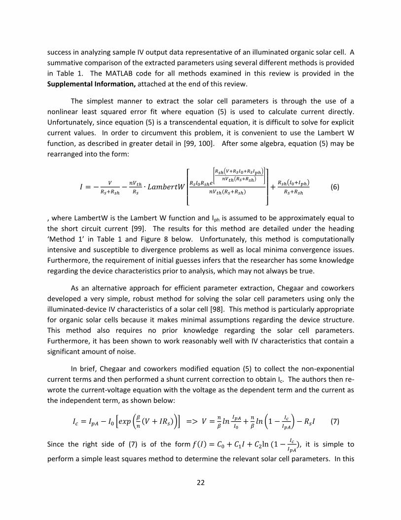
The simplest manner to extract the solar cell parameters is through the use of a
nonlinear least squared error fit where equation (5) is used to calculate current directly.
Unfortunately, since equation (5) is a transcendental equation, it is difficult to solve for explicit
current values. In order to circumvent this problem, it is convenient to use the Lambert W
function, as described in greater detail in [99, 100]. After some algebra, equation (5) may be
rearranged into the form:
(6)
, where LambertW is the Lambert W function and Iph is assumed to be approximately equal to
the short circuit current [99]. The results for this method are detailed under the heading
‘Method 1’ in Table 1 and Figure 8 below. Unfortunately, this method is computationally
intensive and susceptible to divergence problems as well as local minima convergence issues.
Furthermore, the requirement of initial guesses infers that the researcher has some knowledge
regarding the device characteristics prior to analysis, which may not always be true.
As an alternative approach for efficient parameter extraction, Chegaar and coworkers
developed a very simple, robust method for solving the solar cell parameters using only the
illuminated-device IV characteristics of a solar cell [98]. This method is particularly appropriate
for organic solar cells because it makes minimal assumptions regarding the device structure.
This method also requires no prior knowledge regarding the solar cell parameters.
Furthermore, it has been shown to work reasonably well with IV characteristics that contain a
significant amount of noise.
In brief, Chegaar and coworkers modified equation (5) to collect the non-exponential
current terms and then performed a shunt current correction to obtain Ic. The authors then re-
wrote the current-voltage equation with the voltage as the dependent term and the current as
the independent term, as shown below:
(7)
Since the right side of (7) is of the form
, it is simple to
perform a simple least squares method to determine the relevant solar cell parameters. In this

23
particular study, the least squares approach is accomplished through the solution of a system of
equations. This method, denoted ‘Method 2,’ proved to be very quick and yielded
experimentally accurate and relevant data, as shown in Table 1 and Figure 8.
The final method examined in this review is based off of recent work by Nehaoua et. al.
that was aimed to help with parameter determination for organic solar cells [96]. This method
uses a very unique approach to solve for the series resistance and diode ideality factor, which
involves linear regression on a set of data derived from subsets of the initial IV output data.
The reader is encouraged to examine references [96, 101] for a more detailed explanation of
this process. Unfortunately, this method proved to be rather unstable for the sample data
examined in this review. The extracted diode parameters were found to vary strongly
depending on the amount and range of input IV data passed to the MATLAB function.
Regardless, the results are also presented as ‘Method 3’ in Table 1 and Figure 8.
Table 1 - Summary of Extracted Diode Parameters for Different Methods of Analysis on Sample Illuminated IV Organic Solar Cell Data
ISC (A) VOC (V) FF Rsh () Rs () n I0 (A)
Method 1, [99] 0.0064 0.6 0.4902 3.64E+04 38.2436 1.0688 2.21E-12
Method 2, [98] 0.0064 0.6 0.4902 3.63E+04 35.4685 1.3637 2.63E-10
Method 3, [96] 0.0064 0.6 0.4902 3.62E+04 107.4207 3.0274 2.00E-08*
*Method 3 does not provide a reverse saturation current. This value was determined
graphically by attempting to best fit the model to the input data. It is noted that this simple
approach may be an additional cause for error with this method.
Figure 8 - Experimental and Modelled Solar Cell IV Output for Various Methods of Parameter Extraction

24
Method 3 did not converge to realistic or accurate solar cell parameters, in spite of what
appear to be reasonable values in Table 1. It is feasible that the poor behaviour of this method
is simply due to an error in its present implementation. Regardless the methods detailed by
Jain and Kapoor in 2005 [99] and by Bouzidi et. al. in 2007 [98] have shown to provide very
close fits to the illuminated IV data. From the tabulated data in Table 1, it is clear that variation
between series and shunt resistances from both methods 1 and 2 are relatively small, indicating
that cross comparisons between data using either method are valid. However, one should take
precaution when cross-comparing diode ideality factors and reverse saturation current values,
as they are shown to vary by up to ~1.3-times and 2 orders of magnitude respectively between
the two methods for the same data set.
As an additional note, Schilinsky et. al. have examined a modified single-diode model
where the photocurrent, Iph, varies as a function of the applied voltage, such that the model can
account for the field dependence of the photocurrent [102]. The authors note that a similar
approach has been previously successful in the study of amorphous silicon diodes and solar
cells. In typical models, the photocurrent is generally assumed to be equal to the short circuit
current. In contrast, this model defines the photocurrent as shown below, which allows for
accurate measurements over a wider range of illumination intensities.
This variation introduces the free carrier mobility, , the free carrier lifetime, , and the built in
voltage of the junction as additional fitting parameters. While these fitting parameters should
only be taken as estimates of their true values, they may provide crucial information in the
study and comparison of organic solar cells among different research groups.
5. Conclusions: Achieving 10% Efficiency Solar Cells and Beyond
Organic solar cells have seen impressive gains in their device efficiencies over a very
brief period, with most significant improvements achieved only within the past decade. This
rapid progress is largely attributed to initial improvements in device architecture, followed by
strong materials optimization through tailored polymeric donor materials. By shifting from a
single layer solar cell to a planar heterojunction, researchers substantially decreased
bimolecular recombination [18, 27, 28]. This development resulted in the realization of a
donor-acceptor solar cell, which was inherently limited by exciton diffusion to the organic-
organic interface. In order to address this limit, researchers then developed the bulk
heterojunction to decrease the distance an exciton must travel before reaching an interface for
dissociation into free carriers [37-39].

25
The subsequent realization of the P3HT:PCBM bulk heterojunction offered a basis for
developing a stronger understanding for all organic and polymeric photovoltaics [55]. Most
recent work has been dedicated to developing the basic chemistry to reliably fabricate high
efficiency organic solar cells and to forming the physical models to adequately describe bulk
heterojunction device behaviour. As one critical point, researchers have found that the
efficiency of organic solar cells is very strongly controlled by the phase separation and
molecular organization of the donor and acceptor materials. The intensive study of P3HT:PCBM
solar cells has also highlighted a need for researchers to maintain both standard test conditions
and standardized methodologies for solar cell parameter extraction and analysis.
With a better understanding of the organic solar cell fabrication chemistry and device
physics, researchers now have a direct route to improving organic solar cell efficiency. The
ability to custom tailor the HOMO and LUMO of polymers has allowed for the development of
solar cells with specific device output properties in a very controlled manner. This has led to
PTB7-PCBM solar cells with both high open circuit voltages and high short circuit currents,
granting 7.40% power conversion efficiencies [86]. Furthermore, the development of the
integer charge-transfer model provides strong insight into the origin of the open circuit voltage
[41], which may allow for additional gains in device efficiency through optimization of organic-
electrode interfaces.
With the groundwork for highly efficient bulk heterojunction organic solar cells
established, researchers may now begin to examine less straightforward methods to enhance
device efficiency. Such efforts include the development of solution-processable, polymeric
tandem solar cells [103], which may prove to reduce thermalization losses. Researchers have
also begun to use optical spacers to maximize the electric field of impingent light within the
bulk of the active layer [83, 104]. The combination of this work with the optimization of both
device materials and organic-electrode interfaces will ultimately lead to organic solar cells
exceeding 10% efficiency.

26
Works Cited.
[1] P. Kamat, "Meeting the clean energy demand: Nanostructure architectures for solar energy conversion," Journal of Physical Chemistry C, vol. 111, pp. 2834–2860, 2007.
[2] M. Green, et al., "Short Communication Solar cell efficiency tables (version 33)," Progress in Photovoltaics: Research and Applications, vol. 17, pp. 85-94, 2009.
[3] M. Green, et al., "Very high efficiency silicon solar cells-science and technology," Electron Devices, IEEE Transactions on, vol. 46, pp. 1940-1947, 2002.
[4] W. Shockley and H. Queisser, "Detailed Balance Limit of Efficiency of p n Junction Solar Cells," Journal of Applied Physics, vol. 32, pp. 510-519, 1961.
[5] N. Gupta, et al., "Prospects of Nanostructure-Based Solar Cells for Manufacturing Future Generations of Photovoltaic Modules," International Journal of Photoenergy, vol. 1, 2009.
[6] Solar Novus Today. (27 July 2010, Accessed: 9 November 2010). Solarmer Energy, Inc. Breaks Psychological Barrier with 8.13% OPV Efficiency. Available: http://www.solarnovus.com/index.php?option=com_content&view=article&id=1086:solarmer-energy-inc-breaks-psychological-barrier-with-813-opv-efficiency&catid=41:applications-tech-news&Itemid=245
[7] J. G. Xue, et al., "Asymmetric tandem organic photovoltaic cells with hybrid planar-mixed molecular heterojunctions," Applied Physics Letters, vol. 85, pp. 5757-5759, Dec 2004.
[8] J. G. Xue, et al., "4.2% efficient organic photovoltaic cells with low series resistances," Applied Physics Letters, vol. 84, pp. 3013-3015, Apr 2004.
[9] P. Peumans, et al., "Small molecular weight organic thin-film photodetectors and solar cells," Journal of Applied Physics, vol. 93, p. 3693, 2003.
[10] M. Riede, et al., "Small-molecule solar cells - status and perspectives," Nanotechnology, vol. 19, Oct 2008.
[11] H. Spanggaard and F. C. Krebs, "A brief history of the development of organic and polymeric photovoltaics," Solar Energy Materials and Solar Cells, vol. 83, pp. 125-146, Jun 2004.
[12] C. Tang and A. Albrecht, "Photovoltaic effects of metal–chlorophyll a–metal sandwich cells," The Journal of Chemical Physics, vol. 62, p. 2139, 1975.
[13] Y. Gao, et al., "Interface formation of Ca with poly (p phenylene vinylene)," Journal of Applied Physics, vol. 73, pp. 7894-7899, 1993.
[14] H. Antoniadis, et al., "Photovoltaic and Photoconductive Properties of Aluminum Poly(P-Phenylene Vinylene) Interfaces," Synthetic Metals, vol. 62, pp. 265-271, Feb 1994.
[15] W. Riess, et al., "Electroluminescence and photovoltaic effect in PPV schottky diodes," Journal of Luminescence, vol. 60, pp. 906-911, 1994.
[16] R. Marks, et al., "The photovoltaic response in poly (p-phenylene vinylene) thin-film devices," Journal of Physics: Condensed Matter, vol. 6, p. 1379, 1994.
[17] H. Hoppea and N. Sariciftci, "Organic solar cells: An overview," J. Mater. Res, vol. 19, p. 1925, 2004.
[18] C. Tang, "Two layer organic photovoltaic cell," Applied Physics Letters, vol. 48, pp. 183-185, 1986.
27
[19] V. I. Arkhipov, et al., "Why is exciton dissociation so efficient at the interface between a conjugated polymer and an electron acceptor?," Applied Physics Letters, vol. 82, pp. 4605-4607, Jun 2003.
[20] S. A. Jenekhe and S. J. Yi, "Efficient photovoltaic cells from semiconducting polymer heterojunctions," Applied Physics Letters, vol. 77, pp. 2635-2637, Oct 2000.
[21] K. Tada, et al., "Photocell with heterojunction of donor acceptor polymers," Synthetic Metals, vol. 102, pp. 982-983, Jun 1999.
[22] A. J. Breeze, et al., "Polymer-perylene diimide heterojunction solar cells," Applied Physics Letters, vol. 81, pp. 3085-3087, Oct 2002.
[23] J. J. M. Halls and R. H. Friend, "The photovoltaic effect in a poly(p-phenylenevinylene)/perylene heterojunction," Synthetic Metals, vol. 85, pp. 1307-1308, Feb 1997.
[24] J. J. M. Halls, et al., "Exciton diffusion and dissociation in a poly(p-phenylenevinylene)/C-60 heterojunction photovoltaic cell," Applied Physics Letters, vol. 68, pp. 3120-3122, May 1996.
[25] S. Morita, et al., "Wavelength dependence of junction characteristics of poly (3-alkylthiophene)/C60 layer," Japanese Journal of Applied Physics, vol. 32, pp. L873-L874, 1993.
[26] L. S. Roman, et al., "High quantum efficiency polythiophene/C-60 photodiodes," Advanced Materials, vol. 10, pp. 774-777, Jul 1998.
[27] N. Sariciftci, et al., "Semiconducting polymer buckminsterfullerene heterojunctions: Diodes, photodiodes, and photovoltaic cells," Applied Physics Letters, vol. 62, pp. 585-587, 1993.
[28] N. Sariciftci, et al., "Semiconducting polymers (as donors) and buckminsterfullerene (as acceptor): photoinduced electron transfer and heterojunction devices," Synthetic Metals, vol. 59, pp. 333-352, 1993.
[29] N. Sariciftci, et al., "Photoinduced electron transfer from a conducting polymer to buckminsterfullerene," Science, vol. 258, pp. 1474-1476, 1992.
[30] S. Morita, et al., "Doping Effect of Buckminsterfullerene in Conducting Polymer - Change of Absorption-Spectrum and Quenching of Luminescence," Solid State Communications, vol. 82, pp. 249-252, Apr 1992.
[31] C. Lee, et al., "Sensitization of the photoconductivity of conducting polymers by C60: Photoinduced electron transfer," Physical Review B, vol. 48, pp. 15425-15433, 1993.
[32] M. Granstrom, et al., "Laminated fabrication of polymeric photovoltaic diodes," Nature, vol. 395, pp. 257-260, Sep 1998.
[33] J. S. Huang, et al., "A semi-transparent plastic solar cell fabricated by a lamination process," Advanced Materials, vol. 20, pp. 415-+, Feb 2008.
[34] H. Hoppe and N. Sariciftci, "Organic solar cells: An overview," J. Mater. Res, vol. 19, p. 1925, 2004.
[35] G. Yu, et al., "Semiconducting polymer diodes: Large size, low cost photodetectors with excellent visible ultraviolet sensitivity," Applied Physics Letters, vol. 64, pp. 3422-3424, 1994.

28
[36] J. Hummelen, et al., "Preparation and characterization of fulleroid and methanofullerene derivatives," The Journal of Organic Chemistry, vol. 60, pp. 532-538, 1995.
[37] G. Yu, et al., "Polymer photovoltaic cells: enhanced efficiencies via a network of internal donor-acceptor heterojunctions," Science, vol. 270, p. 1789, 1995.
[38] G. Yu and A. Heeger, "Charge separation and photovoltaic conversion in polymer composites with internal donor/acceptor heterojunctions," Journal of Applied Physics, vol. 78, pp. 4510-4515, 1995.
[39] J. J. M. Halls, et al., "Efficient Photodiodes from Interpenetrating Polymer Networks," Nature, vol. 376, pp. 498-500, Aug 1995.
[40] A. Crispin, et al., "Transition between energy level alignment regimes at a low band gap polymer-electrode interfaces," Applied Physics Letters, vol. 89, Nov 2006.
[41] S. Braun, et al., "Energy-Level Alignment at Organic/Metal and Organic/Organic Interfaces," Advanced Materials, vol. 21, pp. 1450-1472, Apr 2009.
[42] S. Sun, "Design of a block copolymer solar cell," Solar Energy Materials and Solar Cells, vol. 79, pp. 257-264, 2003.
[43] F. C. Krebs and M. Jorgensen, "Conducting block copolymers. Towards a polymer pn-junction," Polymer Bulletin, vol. 50, pp. 359-366, Jul 2003.
[44] U. Stalmach, et al., "Semiconducting diblock copolymers synthesized by means of controlled radical polymerization techniques," Journal of the American Chemical Society, vol. 122, pp. 5464-5472, Jun 2000.
[45] B. de Boer, et al., "Supramolecular self-assembly and opto-electronic properties of semiconducting block copolymers," Polymer, vol. 42, pp. 9097-9109, Oct 2001.
[46] Q. Zhang, et al., "Donor- Acceptor Poly (thiophene-block-perylene diimide) Copolymers: Synthesis and Solar Cell Fabrication," Macromolecules, vol. 42, pp. 1079-1082, 2009.
[47] S. E. Shaheen, et al., "2.5% efficient organic plastic solar cells," Applied Physics Letters, vol. 78, pp. 841-843, Feb 2001.
[48] S. Günes, et al., "Conjugated polymer-based organic solar cells," Chem. Rev, vol. 107, pp. 1324-1338, 2007.
[49] C. Melzer, et al., "Hole transport in poly(phenylene vinylene)/methanofullerene bulk-heterojunction solar cells," Advanced Functional Materials, vol. 14, pp. 865-870, Sep 2004.
[50] V. D. Mihailetchi, et al., "Compositional dependence of the performance of poly(p-phenylene vinylene): Methanofullerene bulk-heterojunction solar cells," Advanced Functional Materials, vol. 15, pp. 795-801, May 2005.
[51] J. Kroon, et al., "Accurate efficiency determination and stability studies of conjugated polymer/fullerene solar cells," Thin Solid Films, vol. 403, pp. 223-228, 2002.
[52] T. Munters, et al., "A comparison between state-of-the-art 'gilch' and 'sulphinyl' synthesised MDMO-PPV/PCBM bulk hetero-junction solar cells," Thin Solid Films, vol. 403, pp. 247-251, Feb 2002.
[53] C. J. Brabec, et al., "Effect of LiF/metal electrodes on the performance of plastic solar cells," Applied Physics Letters, vol. 80, pp. 1288-1290, Feb 2002.
[54] E. Bundgaard and F. C. Krebs, "Low band gap polymers for organic photovoltaics," Solar Energy Materials and Solar Cells, vol. 91, pp. 954-985, Jul 2007.

29
[55] P. Schilinsky, et al., "Recombination and loss analysis in polythiophene based bulk heterojunction photodetectors," Applied Physics Letters, vol. 81, pp. 3885-3887, Nov 2002.
[56] F. Padinger, et al., "Effects of postproduction treatment on plastic solar cells," Advanced Functional Materials, vol. 13, pp. 85-88, 2003.
[57] G. Dennler, et al., "Polymer-Fullerene Bulk-Heterojunction Solar Cells," Advanced Materials, vol. 21, pp. 1323-1338, Apr 2009.
[58] C. J. Brabec, et al., "Polymer-Fullerene Bulk-Heterojunction Solar Cells," Advanced Materials, vol. 22, pp. 3839-3856, Sep 2010.
[59] D. Chirvase, et al., "Influence of nanomorphology on the photovoltaic action of polymer–fullerene composites," Nanotechnology, vol. 15, p. 1317, 2004.
[60] I. Riedel and V. Dyakonov, "Influence of electronic transport properties of polymer-fullerene blends on the performance of bulk heterojunction photovoltaic devices," Physica Status Solidi a-Applied Research, vol. 201, pp. 1332-1341, May 2004.
[61] J. S. Huang, et al., "Influence of composition and heat-treatment on the charge transport properties of poly(3-hexylthiophene) and 6,6 -phenyl C-61-butyric acid methyl ester blends," Applied Physics Letters, vol. 87, Sep 2005.
[62] Y. Kim, et al., "Device annealing effect in organic solar cells with blends of regioregular poly(3-hexylthiophene) and soluble fullerene," Applied Physics Letters, vol. 86, Feb 2005.
[63] G. Li, et al., "High-efficiency solution processable polymer photovoltaic cells by self-organization of polymer blends," Nature Materials, vol. 4, pp. 864-868, Nov 2005.
[64] G. Li, et al., "Investigation of annealing effects and film thickness dependence of polymer solar cells based on poly(3-hexylthiophene)," Journal of Applied Physics, vol. 98, Aug 2005.
[65] W. L. Ma, et al., "Thermally stable, efficient polymer solar cells with nanoscale control of the interpenetrating network morphology," Advanced Functional Materials, vol. 15, pp. 1617-1622, Oct 2005.
[66] M. Reyes-Reyes, et al., "High-efficiency photovoltaic devices based on annealed poly(3-hexylthiophene) and 1-(3-methoxycarbonyl)-propyl-1-phenyl-(6,6)C-61 blends," Applied Physics Letters, vol. 87, Aug 2005.
[67] T. J. Savenije, et al., "The effect of thermal treatment on the morphology and charge carrier dynamics in a polythiophene-fullerene bulk heterojunction," Advanced Functional Materials, vol. 15, pp. 1260-1266, Aug 2005.
[68] P. Schilinsky, et al., "Influence of the molecular weight of poly(3-hexylthiophene) on the performance of bulk heterojunction solar cells," Chemistry of Materials, vol. 17, pp. 2175-2180, Apr 2005.
[69] X. N. Yang, et al., "Nanoscale morphology of high-performance polymer solar cells," Nano Letters, vol. 5, pp. 579-583, Apr 2005.
[70] R. C. Hiorns, et al., "High molecular weights, polydispersities, and annealing temperatures in the optimization of bulk-heterojunction photovoltaic cells based on poly(3-hexylthiophene) or poly(3-butylthiophene)," Advanced Functional Materials, vol. 16, pp. 2263-2273, Nov 2006.

30
[71] Y. Kim, et al., "A strong regioregularity effect in self-organizing conjugated polymer films and high-efficiency polythiophene: fullerene solar cells," Nature Materials, vol. 5, pp. 197-203, Mar 2006.
[72] V. D. Mihailetchi, et al., "Origin of the enhanced performance in poly(3-hexylthiophene): 6,6 -phenyl C-61-butyric acid methyl ester solar cells upon slow drying of the active layer," Applied Physics Letters, vol. 89, Jul 2006.
[73] G. Li, et al., ""Solvent annealing" effect in polymer solar cells based on poly(3-hexylthiophene) and methanofullerenes," Advanced Functional Materials, vol. 17, pp. 1636-1644, Jul 2007.
[74] W. Ma, et al., "Effect of the molecular weight of poly(3-hexylthiophene) on the morphology and performance of polymer bulk heterojunction solar cells," Macromolecular Rapid Communications, vol. 28, pp. 1776-1780, Sep 2007.
[75] A. J. Moule and K. Meerholz, "Controlling morphology in polymer-fullerene mixtures," Advanced Materials, vol. 20, pp. 240-+, Jan 2008.
[76] M. Svensson, et al., "High-performance polymer solar cells of an alternating polyfluorene copolymer and a fullerene derivative," Advanced Materials, vol. 15, pp. 988-+, Jun 2003.
[77] F. L. Zhang, et al., "Influence of solvent mixing on the morphology and performance of solar cells based on polyfluorene copolymer/fullerene blends," Advanced Functional Materials, vol. 16, pp. 667-674, Mar 2006.
[78] L. H. Slooff, et al., "Determining the internal quantum efficiency of highly efficient polymer solar cells through optical modeling," Applied Physics Letters, vol. 90, Apr 2007.
[79] E. G. Wang, et al., "High-performance polymer heterojunction solar cells of a polysilafluorene derivative," Applied Physics Letters, vol. 92, Jan 2008.
[80] M. H. Chen, et al., "Efficient Polymer Solar Cells with Thin Active Layers Based on Alternating Polyfluorene Copolymer/Fullerene Bulk Heterojunctions," Advanced Materials, vol. 21, pp. 4238-+, Nov 2009.
[81] N. Blouin, et al., "A low-bandgap poly(2,7-carbazole) derivative for use in high-performance solar cells," Advanced Materials, vol. 19, pp. 2295-+, Sep 2007.
[82] N. Blouin, et al., "Toward a rational design of poly(2,7-carbazole) derivatives for solar cells," Journal of the American Chemical Society, vol. 130, pp. 732-742, Jan 2008.
[83] S. H. Park, et al., "Bulk heterojunction solar cells with internal quantum efficiency approaching 100%," Nature Photonics, vol. 3, pp. 297-U5, May 2009.
[84] Y. Y. Liang, et al., "Highly Efficient Solar Cell Polymers Developed via Fine-Tuning of Structural and Electronic Properties," Journal of the American Chemical Society, vol. 131, pp. 7792-7799, Jun 2009.
[85] Y. Y. Liang, et al., "Development of New Semiconducting Polymers for High Performance Solar Cells," Journal of the American Chemical Society, vol. 131, pp. 56-+, Jan 2009.
[86] Y. Liang, et al., "For the bright future—bulk heterojunction polymer solar cells with power conversion efficiency of 7.4%," Advanced Materials, vol. 22, pp. E135-E138, 2010.
[87] J. Guo, et al., "Structure, Dynamics, and Power Conversion Efficiency Correlations in a New Low Bandgap Polymer: PCBM Solar Cell," The Journal of Physical Chemistry B, vol. 114, pp. 742-748, 2009.
31
[88] A. Cravino, "Origin of the open circuit voltage of donor-acceptor solar cells: Do polaronic energy levels play a role?," Applied Physics Letters, vol. 91, Dec 2007.
[89] C. J. Brabec, et al., "Origin of the open circuit voltage of plastic solar cells," Advanced Functional Materials, vol. 11, pp. 374-380, Oct 2001.
[90] M. Scharber, et al., "Design Rules for Donors in Bulk Heterojunction Solar Cells—Towards 10% Energy Conversion Efficiency," Advanced Materials, vol. 18, pp. 789-794, 2006.
[91] B. Rand, et al., "Offset energies at organic semiconductor heterojunctions and their influence on the open-circuit voltage of thin-film solar cells," Physical Review B, vol. 75, p. 115327, 2007.
[92] S. Shaheen, et al., "Effects of inserting highly polar salts between the cathode and active layer of bulk heterojunction photovoltaic devices," in Materials Research Society Symposium, San Francisco, California, 2001, pp. 219-226.
[93] S. Jonsson, et al., "Photoelectron spectroscopy of the contact between the cathode and the active layers in plastic solar cells: the role of LiF," Japanese Journal of Applied Physics Part 1: Regular Papers, Short Notes and Review Papers, vol. 44, p. 3695, 2005.
[94] F. Shirland, "The history, design, fabrication and performance of CdS thin film solar cells," Advanced Energy Conversion, vol. 6, pp. 201-202, 1966.
[95] Z. Ouennoughi and M. Chegaar, "A simpler method for extracting solar cell parameters using the conductance method," Solid-State Electronics, vol. 43, pp. 1985-1988, 1999.
[96] N. Nehaoua, et al., "Determination of organic solar cell parameters based on single or multiple pin structures," Vacuum, vol. 84, pp. 326-329, 2009.
[97] M. Chegaar, et al., "Simple parameter extraction method for illuminated solar cells," Solid-State Electronics, vol. 50, pp. 1234-1237, 2006.
[98] K. Bouzidi, et al., "Solar cells parameters evaluation considering the series and shunt resistance," Solar Energy Materials and Solar Cells, vol. 91, pp. 1647-1651, 2007.
[99] A. Jain and A. Kapoor, "A new method to determine the diode ideality factor of real solar cell using Lambert W-function," Solar Energy Materials and Solar Cells, vol. 85, pp. 391-396, 2005.
[100] A. Jain and A. Kapoor, "A new approach to study organic solar cell using Lambert W-function," Solar Energy Materials and Solar Cells, vol. 86, pp. 197-205, 2005.
[101] A. Kaminski, et al., "Non ideal dark IV curves behavior of silicon solar cells," Solar Energy Materials and Solar Cells, vol. 51, pp. 221-231, 1998.
[102] P. Schilinsky, et al., "Simulation of light intensity dependent current characteristics of polymer solar cells," Journal of Applied Physics, vol. 95, pp. 2816-2819, Mar 2004.
[103] J. Kim, et al., "Efficient tandem polymer solar cells fabricated by all-solution processing," Science, vol. 317, p. 222, 2007.
[104] J. Y. Kim, et al., "New architecture for high-efficiency polymer photovoltaic cells using solution-based titanium oxide as an optical spacer," Advanced Materials, vol. 18, pp. 572-+, Mar 2006.

32
Supplemental Information
The MATLAB code used in the solar cell parameter extraction, as detailed in Section 4, is copied
below. If the reader would like a copy of the “.m” function files or the data set used in this
analysis, he or she may contact Graeme Williams at [email protected].
Method 1
Jain2005.m
function [ ] = Jain2005(IVData)
%This function calculates all of the relevant solar cell parameters given
%an input matrix IVData containing data in the form [Voltage Current]
%This script uses a very simple sum of squared approach to converge toward
%the ideal fitting parameters. This script requires initial guess values.
%Constants
q = 1.602*10^-19;
k = 1.38*10^-23;
T = 298;
beta = q./(k.*T);
Vth = 1./beta;
global I V Isc Rsh
%--------------------------------------------------------------------------
%Breaking apart input matrix
V=IVData(:,1);
I=IVData(:,2);
%Finding the Isc (foo is a dummy variable)
[foo, SCindex] = min(abs(V));
Isc = I(SCindex);
%Finding the Voc
[foo, OCindex] = min(abs(I));
Voc = V(OCindex);
%Selecting the region of interest for the input data
V=IVData(SCindex+6:OCindex-1,1);
I=IVData(SCindex+6:OCindex-1,2);
%Using the slope at V=0V as Rsh (otherwise the function is under-defined and
%diverges)
Vlin=IVData(1:SCindex+1,1);
Ilin=IVData(1:SCindex+1,2);
[f,err] = polyfit(Vlin, Ilin,1);
Gsh = -f(1); %Defining the shunt resistance as the slope
Rsh = 1./Gsh;
%Initial guess values
Rs = 10;
n = 2;
I0 = 1*10^-10;
a= [Rs; n; I0];
%Calculating the modelling variables by minimizing SSE (using a
%user-defined function that takes the input data + initial guesses and

33
%outputs the sum of squared error)
solved = fminsearch(@diode_minerr, a);
%----------------------------------
%Fill factor and power calculations
V=IVData(:,1);
I=IVData(:,2);
Vmod = V(SCindex:OCindex);
Imod = I(SCindex:OCindex);
P = Vmod.*Imod;
[Pmax,Pmaxpt] = max(abs(P));
Vprime = Vmod(Pmaxpt);
Iprime = Imod(Pmaxpt);
FF = (Iprime.*Vprime)./(Voc.*Isc);
%----------------------------------
%Outputting relevant data
Isc
Voc
FF
Rsh
Rs = solved(1)
n = solved(2)
I0 = solved(3)
diode_minerr.m
function SSE = diode_minerr(a)
%This function requires the (global) data from the IV characteristics and
%the initial guesses for the fitting parameters. It calculates the
%error between the diode-Rs-Rsh model and the experimental IV values.
%The rearranged, explicitly solved current equation (making use of the
%Lambert W function) was taken from Jain & Kapoor, 2005, "A new method to
%determine the diode ideality factor of real solar cell using Lambert
%W-function"
%Variables
q = 1.602*10^-19;
k = 1.38*10^-23;
T = 298;
beta = q./(k.*T);
Vth = 1./beta;
global I V Isc Rsh
%Exploding the a variable
Rs = a(1);
n = a(2);
I0 = a(3);
%Prediction of the current using the Lambert W function
Ipred = -V./(Rs+Rsh)-
lambertw(((Rs.*I0.*Rsh).*exp((Rsh.*(Rs.*Isc+Rs.*I0+V))./(n.*Vth.*(Rs+Rsh))))./(Rs.*n.*
Vth+Rsh.*n.*Vth)).*(n.*Vth)./Rs + Rsh.*(I0+Isc)./(Rs+Rsh);
%Calculating sum of square errors
SSE = sum((Ipred-I).^2);
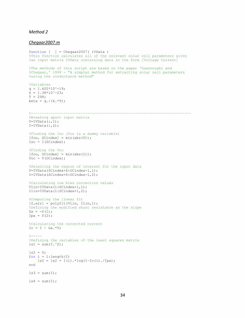
34
Method 2
Chegaar2007.m
function [ ] = Chegaar2007( IVData )
%This function calculates all of the relevant solar cell parameters given
%an input matrix IVData containing data in the form [Voltage Current]
%The methods of this script are based on the paper 'Ouennoughi and
%Chegaar,' 1999 - "A simpler method for extracting solar cell parameters
%using the conductance method"
%Variables
q = 1.602*10^-19;
k = 1.38*10^-23;
T = 298;
beta = q./(k.*T);
%--------------------------------------------------------------------------
%Breaking apart input matrix
V=IVData(:,1);
I=IVData(:,2);
%Finding the Isc (foo is a dummy variable)
[foo, SCindex] = min(abs(V));
Isc = I(SCindex);
%Finding the Voc
[foo, OCindex] = min(abs(I));
Voc = V(OCindex);
%Selecting the region of interest for the input data
V=IVData(SCindex+6:OCindex-1,1);
I=IVData(SCindex+6:OCindex-1,2);
%Calculating low bias correction values
Vlin=IVData(1:SCindex+1,1);
Ilin=IVData(1:SCindex+1,2);
%Computing the linear fit
[f,err] = polyfit(Vlin, Ilin,1);
%Defining the modified shunt resistance as the slope
Ga = -f(1);
Ipa = f(2);
%Calculating the corrected current
Ic = I - Ga.*V;
%-----
%Defining the variables of the least squares matrix
ls1 = sum(I.^2);
ls2 = 0;
for i = 1:length(I)
ls2 = ls2 + I(i).*log(1-Ic(i)./Ipa);
end
ls3 = sum(I);
ls4 = sum(I);

35
ls5 = 0;
for i = 1:length(I)
ls5 = ls5 + log(1-Ic(i)./Ipa);
end
ls6 = length(I);
ls7 = 0;
for i = 1:length(I)
ls7 = ls7 + I(i).*log(1-Ic(i)./Ipa);
end
ls8 = 0;
for i = 1:length(I)
ls8 = ls8 + (log(1-Ic(i)./Ipa)).^2;
end
ls9 = 0;
for i = 1:length(I)
ls9 = ls9 + log(1-Ic(i)./Ipa);
end
lsmatrix = [ls1 ls2 ls3; ls4 ls5 ls6; ls7 ls8 ls9];
%------
a1 = sum(I.*V);
a2 = sum(V);
a3 = 0;
for i = 1:length(I)
a3 = a3 + V(i).*log(1-Ic(i)./Ipa);
end
amatrix = [a1; a2; a3];
%Solving for the variables of the least squares matrix
C = linsolve(lsmatrix,amatrix);
%Solving for various parameters
Rs = -C(1); %series resistance
n = beta.*C(2); %diode ideality coefficient
I0 = Ipa.*exp(-C(3)./C(2)); %I0
foo = 1 - Ga.*Rs; %dummy variable
Gsh = Ga./foo; %shunt conductance
Rsh = 1./Gsh; %shunt resistance
Iph = Ipa./foo; %photocurrent
Is = I0./foo; %saturation current
%----------------------------------
%Fill factor and power calculations
V=IVData(:,1);
I=IVData(:,2);
Vmod = V(SCindex:OCindex);
Imod = I(SCindex:OCindex);
P = Vmod.*Imod;
[Pmax,Pmaxpt] = max(abs(P));
Vprime = Vmod(Pmaxpt);
Iprime = Imod(Pmaxpt);
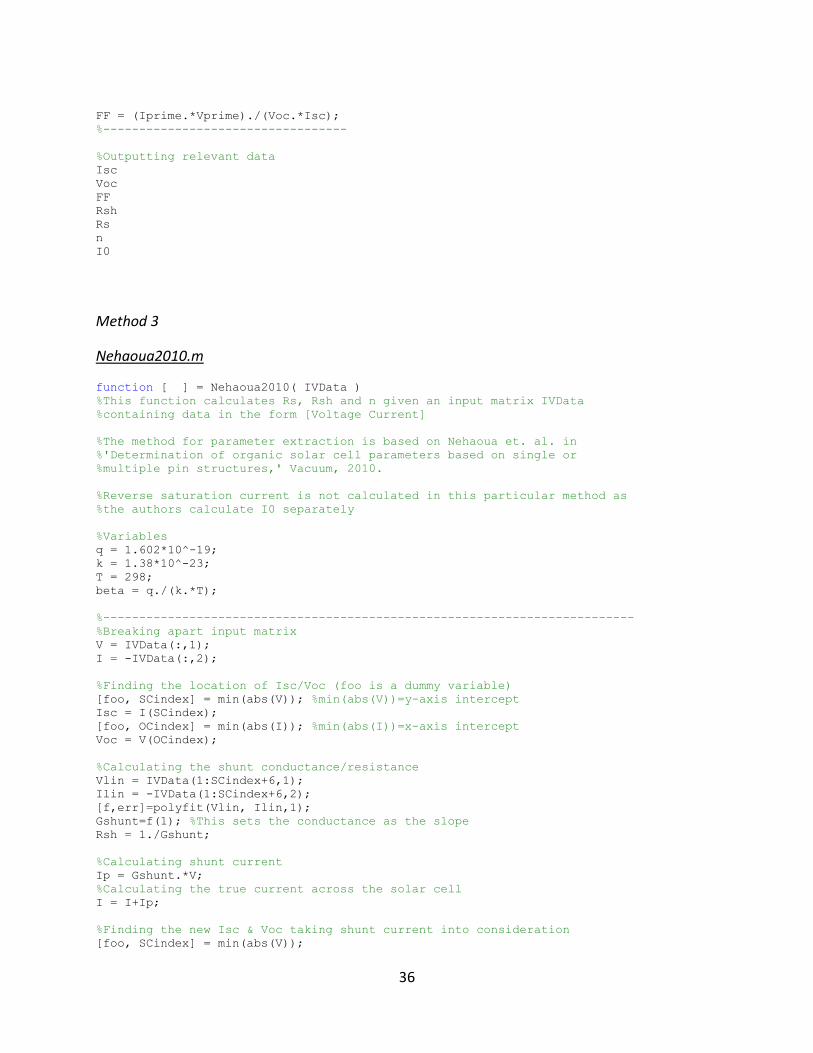
36
FF = (Iprime.*Vprime)./(Voc.*Isc);
%----------------------------------
%Outputting relevant data
Isc
Voc
FF
Rsh
Rs
n
I0
Method 3
Nehaoua2010.m
function [ ] = Nehaoua2010( IVData )
%This function calculates Rs, Rsh and n given an input matrix IVData
%containing data in the form [Voltage Current]
%The method for parameter extraction is based on Nehaoua et. al. in
%'Determination of organic solar cell parameters based on single or
%multiple pin structures,' Vacuum, 2010.
%Reverse saturation current is not calculated in this particular method as
%the authors calculate I0 separately
%Variables
q = 1.602*10^-19;
k = 1.38*10^-23;
T = 298;
beta = q./(k.*T);
%--------------------------------------------------------------------------
%Breaking apart input matrix
V = IVData(:,1);
I = -IVData(:,2);
%Finding the location of Isc/Voc (foo is a dummy variable)
[foo, SCindex] = min(abs(V)); %min(abs(V))=y-axis intercept
Isc = I(SCindex);
[foo, OCindex] = min(abs(I)); %min(abs(I))=x-axis intercept
Voc = V(OCindex);
%Calculating the shunt conductance/resistance
Vlin = IVData(1:SCindex+6,1);
Ilin = -IVData(1:SCindex+6,2);
[f,err]=polyfit(Vlin, Ilin,1);
Gshunt=f(1); %This sets the conductance as the slope
Rsh = 1./Gshunt;
%Calculating shunt current
Ip = Gshunt.*V;
%Calculating the true current across the solar cell
I = I+Ip;
%Finding the new Isc & Voc taking shunt current into consideration
[foo, SCindex] = min(abs(V));

37
Isc = I(SCindex);
[foo, OCindex] = min(abs(I));
Voc = V(OCindex);
%Fill factor and power calculations
Vmod = V(SCindex:OCindex);
Imod = I(SCindex:OCindex);
P = Vmod.*Imod;
[Pmax,Pmaxpt] = max(abs(P));
Vprime = Vmod(Pmaxpt);
Iprime = Imod(Pmaxpt);
FF = (Iprime.*Vprime)./(Voc.*Isc);
%----------------------------------
%Rshunt, Rseries and n
%Redefining the range of data - only focusing on the region of 'diode'
%behaviour
V = IVData(1:OCindex-1,1);
I = -IVData(1:OCindex-1,2);
%Calculating shunt current
Ip = Gshunt.*V;
%Calculating the current across the solar cell
I = I+Ip;
%Solving for the linear regression parameters
X = [];
Y = [];
Iph = Isc; %Ishort circuit approximately equals photocurrent
for i = 1:(length(V)-1)
for j = (i+1):length(V)
if abs(Iph) > abs(I(j)) %Protection from noise, which can cause |I| > |Isc|
if abs(Iph) > abs(I(i)) %Same as above
X = [X; (V(j)-V(i))./(I(j)-I(i))];
Y = [Y; (1./(I(j)-I(i))).*log((Iph-I(j))./(Iph-I(i)))];
end
end
end
end
%Computing the linear fit
[f,err] = polyfit(X,Y,1);
%Solving for pertinent data
slope = f(1);
yint = f(2);
nval = beta./slope;
Rs = nval.*yint./beta;
%Outputting the relevant data
Isc
Voc
FF
Rsh
Rs
nval

38
Plotting Function
Plotting.m
function [ ] = Plotting( IVData, SolvedParam )
%Variables
q = 1.602*10^-19;
k = 1.38*10^-23;
T = 298;
beta = q./(k.*T);
Vth = 1./beta;
%Breaking apart input matrix
V=IVData(:,1);
I=IVData(:,2);
%Generic Solved Data
Isc = SolvedParam(1,1);
Voc = SolvedParam(1,2);
FF = SolvedParam(1,3);
%Method-specific Data
%Method 1
m1_Rsh = SolvedParam(1,4);
m1_Rs = SolvedParam(1,5);
m1_n = SolvedParam(1,6);
m1_I0 = SolvedParam(1,7);
%Method 2
m2_Rsh = SolvedParam(2,4);
m2_Rs = SolvedParam(2,5);
m2_n = SolvedParam(2,6);
m2_I0 = SolvedParam(2,7);
%Method 3
m3_Rsh = SolvedParam(3,4);
m3_Rs = SolvedParam(3,5);
m3_n = SolvedParam(3,6);
m3_I0 = SolvedParam(3,7);
%Creating a separate folder in which to save the figures
mkdir('DataFigures');
figsavepath = ['DataFigures\'];
%Model 1
Rsh = m1_Rsh;
Rs = m1_Rs;
n = m1_n;
I0 = m1_I0;
%Generating the model data
Ipred1 = -V./(Rs+Rsh)-
lambertw(((Rs.*I0.*Rsh).*exp((Rsh.*(Rs.*Isc+Rs.*I0+V))./(n.*Vth.*(Rs+Rsh))))./(Rs.*n.*
Vth+Rsh.*n.*Vth)).*(n.*Vth)./Rs + Rsh.*(I0+Isc)./(Rs+Rsh);
%Model 2
Rsh = m2_Rsh;
Rs = m2_Rs;
n = m2_n;
I0 = m2_I0;
%Generating the model data

39
Ipred2 = -V./(Rs+Rsh)-
lambertw(((Rs.*I0.*Rsh).*exp((Rsh.*(Rs.*Isc+Rs.*I0+V))./(n.*Vth.*(Rs+Rsh))))./(Rs.*n.*
Vth+Rsh.*n.*Vth)).*(n.*Vth)./Rs + Rsh.*(I0+Isc)./(Rs+Rsh);
%Model 3
Rsh = m3_Rsh;
Rs = m3_Rs;
n = m3_n;
I0 = m3_I0;
%Generating the model data
Ipred3 = -V./(Rs+Rsh)-
lambertw(((Rs.*I0.*Rsh).*exp((Rsh.*(Rs.*Isc+Rs.*I0+V))./(n.*Vth.*(Rs+Rsh))))./(Rs.*n.*
Vth+Rsh.*n.*Vth)).*(n.*Vth)./Rs + Rsh.*(I0+Isc)./(Rs+Rsh);
%Creating a filename
figname = [figsavepath 'PlotComparison' '.png'];
figsave = figure;
p = plot(V,I,'o'); %Plotting experimental data
set(p,'Color','red')
hold on
q = plot(V,Ipred1,'-'); %Plotting Method 1
set(q,'Color','blue','LineWidth',2)
r = plot(V,Ipred2,'-'); %Plotting Method 2
set(r,'Color','black','LineWidth',2)
s = plot(V,Ipred3,'-'); %Plotting Method 3
set(s,'Color','green','LineWidth',2)
xlabel('V (V)');
ylabel('I (A)');
legend('Data Set', 'Method 1', 'Method 2', 'Method 3');
print(figsave, figname, '-dpng');
end