advances in optics: reviews book series, volume...
TRANSCRIPT

Advances in Optics: Reviews
Book Series, Volume 2


Sergey Y. Yurish Editor
Advances in Optics: Reviews
Book Series, Volume 2
International Frequency Sensor Association Publishing

Sergey Y. Yurish Editor Advances in Optics: Reviews Book Series, Vol. 2
Published by International Frequency Sensor Association (IFSA) Publishing, S. L., 2018 E-mail (for print book orders and customer service enquires): [email protected] Visit our Home Page on http://www.sensorsportal.com Advances in Optics: Reviews, Vol. 2 is an open access book which means that all content is freely available without charge to the user or his/her institution. Users are allowed to read, download, copy, distribute, print, search, or link to the full texts of the articles, or use them for any other lawful purpose, without asking prior permission from the publisher or the authors. This is in accordance with the BOAI definition of open access.
Neither the authors nor International Frequency Sensor Association Publishing accept any responsibility or liability for loss or damage occasioned to any person or property through using the material, instructions, methods or ideas contained herein, or acting or refraining from acting as a result of such use. ISBN: 978-84-697-9437-1 e-ISBN: 978-84-697-9438-8 BN-20180420-XX BIC: TTB

Acknowledgments
As Editor I would like to express my undying gratitude to all authors, editorial staff, reviewers and others who actively participated in this book. We want also to express our gratitude to all their families, friends and colleagues for their help and understanding.


Contents
7
Contents
Contents ............................................................................................................................ 7 Contributors................................................................................................................... 13 Preface ............................................................................................................................ 17 1. Laser Bending ............................................................................................................ 19
1.1. Introduction ...................................................................................................................... 19 1.2. Laser Bending .................................................................................................................. 20
1.2.1. Laser Bending Mechanisms .................................................................................................. 22 1.2.2. Numerical Simulation ........................................................................................................... 24 1.2.3. Main Effect Factors .............................................................................................................. 28 1.2.4. Optimization Laser Manufacture Parameters ....................................................................... 32
1.3. Laser Preloaded Bending ................................................................................................. 37 1.3.1. Principle of Laser Preloaded Bending .................................................................................. 37 1.3.2. Characteristics of Laser Preloaded Bending ........................................................................ 39 1.3.3. Application of Laser Preloaded Bending .............................................................................. 44
1.4. Conclusions ...................................................................................................................... 48 Acknowledgements ................................................................................................................. 48 References ............................................................................................................................... 48
2. Coherent Beam Combining as an Approach to Extend Achievable Limits of Laser Systems ....................................................................................................... 53
2.1. Introduction ...................................................................................................................... 53 2.2. Coherent Combining Approaches and Geometries .......................................................... 54 2.3. Efficiency of the Coherent Beam Combining .................................................................. 56 2.4. The Importance of the Filling Factor for the Far-Field Combining ................................. 58 2.5. Stabilization Approaches .................................................................................................. 60 2.6. State of the Art Achievements in the Coherent Beam Combining and Ongoing
Projects ............................................................................................................................ 63 2.7. Conclusions ...................................................................................................................... 64 References ............................................................................................................................... 65
3. Ultrafast X-Ray Pump-Probe Investigation of Molecular Dynamics with Free Electron Laser Pulses ............................................................................. 67
3.1. Overview .......................................................................................................................... 67 3.2. Design of the Soft X-Ray LCLS Split and Delay Apparatus ........................................... 69
3.2.1. Working Principle of the XRSD Instrument .......................................................................... 69 3.2.2. Technical Realization of the XRSD Instrumental Motion ..................................................... 73 3.2.3. Setting the Time Delays of the XRSD Instrument .................................................................. 73
3.3. Investigating Charge and Dissociation Dynamics in Methyl Iodide Using the XRSD Device ............................................................................................................................. 74 3.3.1. Background ........................................................................................................................... 74 3.3.2. Experiment and Analysis Method .......................................................................................... 76 3.3.3. Experimental Results ............................................................................................................ 77

Advances in Optics: Reviews. Book Series, Vol. 2
8
3.3.3.1. Evolution of the Charge State Distribution ................................................................. 77 3.3.3.2. Evolution of the Ion Kinetic Energy Distribution ....................................................... 80 3.3.3.3. Discussion .................................................................................................................. 83
3.4. Conclusion ........................................................................................................................ 85 Acknowledgements .................................................................................................................. 86 References ............................................................................................................................... 86
4. Single-Shot Auto and Cross Correlation Schemes for Ultrashort Laser Pulse Measurement Using Random Nonlinear Crystals ....................................... 89
4.1. Introduction ....................................................................................................................... 89 4.2. Second Harmonic Generation in Random Nonlinear Crystals .......................................... 91 4.3. Auto-Correlation Scheme: Measurement of Ultrashort Pulse Temporal Duration
and Chirp Parameter ........................................................................................................ 93 4.3.1. Experimental Set-Up ............................................................................................................. 94 4.3.2. Theoretical Model ................................................................................................................. 95 4.3.3. Measurements of the Pulse Durations of the Order of 200 fs ................................................ 96 4.3.4. Measurements of Pulse Durations and Chirp Parameter for Pulses Down to 30 fs ............. 98
4.4. Transverse Single Shot Cross-Correlation Scheme: Laser Pulse Temporal Shape Measurement .................................................................................................................. 101
4.5. Limitations of the Technique .......................................................................................... 105 4.6. Conclusions ..................................................................................................................... 107 Acknowledgements ................................................................................................................ 108 References ............................................................................................................................. 108
5. Modeling the Interaction of Laser Beams with Plasma by using the FDTD Method .................................................................................................. 113
5.1. Introduction ..................................................................................................................... 113 5.2. Physical Models of Plasma ............................................................................................. 114
5.2.1. Linear Drude Model ............................................................................................................ 114 5.2.2. Nonlinear Drude Model ...................................................................................................... 115
5.3. FDTD Implementations of Models ................................................................................. 116 5.3.1. Implementation of Linear Drude Model .............................................................................. 116 5.3.2. Implementation of Nonlinear Drude Model ........................................................................ 117
5.4. Numerical Laser Beam Generation ................................................................................. 119 5.5. Numerical Examples and Results ................................................................................... 121
5.5.1. Low-power Gaussian Laser Beam ...................................................................................... 121 5.5.2. High-power Gaussian Laser Beam ..................................................................................... 121 5.5.3. High-power Vortex Laguerre-Gaussian Laser Beam .......................................................... 124
5.6. Conclusions ..................................................................................................................... 125 Acknowledgements ................................................................................................................ 126 References ............................................................................................................................. 126
6. Laser Separation and Recovery of Rare Earth Elements from Coal Ashes ....... 129
6.1. Introduction ..................................................................................................................... 129 6.2. Laser Radiation Forces ................................................................................................... 129 6.3. Laser-Induced Motion of Particles .................................................................................. 136 6.4. Laser Separation and Recovery of Rare Earth Elements from Coal Ashes ................... 137

Contents
9
6.5. Experimental Observations ............................................................................................ 140 6.6. Conclusions .................................................................................................................... 142 Acknowledgement................................................................................................................. 143 References ............................................................................................................................. 143
7. Relativistic Photoionization Driven by Short Laser Pulses ................................. 145
7.1. Introduction .................................................................................................................... 145 7.2. Relativistic Strong-Field Approximation ....................................................................... 146
7.2.1. Probability Amplitude of Ionization in the RSFA ................................................................ 148 7.2.2. Probability Amplitude of Ionization in the Saddle-Point Approximation ............................ 152 7.2.3. Laser Pulse and Its Characteristics .................................................................................... 155 7.2.4. Approximate Solution to the Saddle-Point Equation ........................................................... 157
7.3. Spiral of Ionization in Momentum Space ....................................................................... 159 7.3.1. Probability of Ionization along the Three-Dimensional Momentum Spiral ........................ 161
7.4. Energy Spectra of Photoelectrons .................................................................................. 164 7.5. Energy-Angular Probability Distributions ..................................................................... 166 7.6. Application: Generation of Single-Electron Wave Packets ............................................ 169 7.7. Conclusions .................................................................................................................... 173 Acknowledgements ............................................................................................................... 174 References ............................................................................................................................. 174
8. Direct Femtosecond Laser Writing of Nonlinear Photonic Crystals ................. 177
8.1. Quasi-Phase Matching and Nonlinear Photonic Crystals ............................................... 177 8.2. Traditional Fabrication Methods of Nonlinear Photonic Crystals .................................. 178
8.2.1. Electric Field Poling ........................................................................................................... 179 8.2.2. UV Light Poling .................................................................................................................. 180 8.2.3. Other Poling Techniques .................................................................................................... 180
8.3. Direct Femtosecond Infrared Laser Writing of Ferroelectric Domain Patterns ............. 180 8.4. Application of Femtosecond-Laser-Written Domain Patterns in Nonlinear Optics ...... 185 8.5. Conclusions .................................................................................................................... 188 Acknowledgements ............................................................................................................... 188 References ............................................................................................................................. 188
9. Linearization of a LTE Radio-over-Fiber Fronthaul System based on Optimized Genetic Algorithm CPWL Models ..................................... 193
9.1. Introduction .................................................................................................................... 193 9.2. Proposed Models ............................................................................................................ 194
9.2.1. Volterra Model .................................................................................................................... 194 9.2.2. CPWL Model ...................................................................................................................... 196 9.2.3. Threshold Optimization with Genetic Algorithms ............................................................... 197 9.2.4. Computational Cost Overview ............................................................................................ 199
9.2.4.1. Volterra Model ......................................................................................................... 199 9.2.4.2. CPWL Model ........................................................................................................... 200 9.2.4.3. GA-CPWL Model .................................................................................................... 202
9.3. Experimental Results without Optimization .................................................................. 203 9.3.1. Experimental Setup ............................................................................................................. 203 9.3.2. RoF Modeling Results ......................................................................................................... 203 9.3.3. DPD Identification Results ................................................................................................. 204

Advances in Optics: Reviews. Book Series, Vol. 2
10
9.4. Experimental Results with Threshold Optimization ....................................................... 206 9.4.1. Experimental Setup ............................................................................................................. 206 9.4.2. DPD Identification Results.................................................................................................. 208
9.5. Conclusions ..................................................................................................................... 213 Acknowledgements ................................................................................................................ 213 References ............................................................................................................................. 213
10. Embedding the Photon with Its Relativistic Mass as a Particle into the Electromagnetic Wave ............................................................................. 215
10.1. Introduction ................................................................................................................... 215 10.2. Derivation of a Transverse Force Exerted on a Photon Propagating
with an Electromagnetic Wave ...................................................................................... 216 10.3. Derivation of a Potential and a Schrödinger Equation Describing
the Transverse Motion of the Photon ............................................................................. 220 10.4. Verification of the Eqs. (10.9), (10.10) and (10.11) for the Case
of the Plane, the Spherical, and the Gaussian Wave ...................................................... 222 10.5. Quantum Mechanical Computation of the Gouy Phase Shift for the Case
of a Gaussian Wave ....................................................................................................... 226 10.6. Ray Optics Confirmation of the Frequency ω Describing the Transverse
Motion of a Photon Moving with a Gaussian Beam ...................................................... 228 10.7. Snell's Law Derived from a Particle Picture ................................................................. 229 10.8. The Schrödinger Equation Describing the Transverse Quantum Mechanical
Motion of a Photon in a Medium ................................................................................... 230 10.9. Summary and Conclusions ........................................................................................... 231 References ............................................................................................................................. 232
11. Proposal of a Bidirectional Microwave Photonic Filter Architecture for Simultaneous Transmission of Digital TV Signal .......................................... 235
11.1. Introduction ................................................................................................................... 235 11.2. Operation Principle ....................................................................................................... 236 11.3. Experimental Setup and Results ................................................................................... 241
11.3.1. Bidirectional Frequency Response .................................................................................... 241 11.3.2. Bidirectional Digital TV Signal Transmission .................................................................. 244
11.4. Conclusions ................................................................................................................... 247 Acknowledgements ................................................................................................................ 247 References ............................................................................................................................. 247
12. Integration of Vertical 1D Photonic Crystals and Photovoltaics ...................... 249
12.1. Background/Overview .................................................................................................. 249 12.1.1. Photovoltaics ..................................................................................................................... 249
12.1.1.1. Need for Renewable Energy ................................................................................... 249 12.1.1.2. Current State of Solar Photovoltaics ....................................................................... 250 12.1.1.3. Optical Absorption Constraints in Thin Film Technologies ................................... 251 12.1.1.4. Enhancing Light Absorption in Thin Films ............................................................ 254 12.1.1.5. Improving the Optical Performance of PV Cells with Photonic Crystals ............... 255
12.1.2. Photonic Crystals .............................................................................................................. 256 12.1.2.1. Historical Background ............................................................................................ 256 12.1.2.2. Properties of Photonic Crystals ............................................................................... 257

Contents
11
12.2. Designing 1D Photonic Crystal Reflectors for Thin-Film PV Cells ............................ 259 12.2.1. Fabricating Bragg Reflectors with TCOs and NPs ........................................................... 259
12.2.1.1. Material Selection ................................................................................................... 259 12.2.1.2. Transparent Conductive Oxides ............................................................................. 259 12.2.1.3. TCO/Nanoparticle Bi-Layers.................................................................................. 262
12.2.2. The Bragg Stack as Selectively Transparent and Conductive Photonic Crystals .............. 263 12.2.2.1. The Optical Properties of STCPCs ......................................................................... 263 12.2.2.2. Electronic Behavior of STCPCs ............................................................................. 264
12.2.3. Introducing Gratings to 1D Bragg Stacks for 1.5D Architecture...................................... 266
12.3. Integrating 1D Photonic Crystal Reflectors within Thin-Film PV Cells ...................... 267 12.3.1. Application in Silicon Photovoltaics ................................................................................. 267
12.3.1.1. Background on Micromorph Tandem Cell ............................................................. 267 12.3.1.2. Selectively Transparent PCs in Micromorph Cells ................................................. 268 12.3.1.3. Background on Ultra-Thin Silicon Films ............................................................... 271 12.3.1.4. Broadband 1D PCs on Single Layer Ultra-Thin Silicon ......................................... 272
12.4. Photonic Crystals for Building Integrated PV Applications ......................................... 274 12.4.1. The Need for Energy Self-Sufficiency in Buildings ........................................................... 274 12.4.2. The Use of 1D PCs in PV Cells Suitable for BIPV Applications ....................................... 275
12.5. Conclusion and Future Potentialities ............................................................................ 276 Acknowledgements ............................................................................................................... 277 References ............................................................................................................................. 277
13. Crystal and Quasicrystal Lattice Solitons in NLSM Equation ........................ 283
13.1. Introduction .................................................................................................................. 283 13.1.1. Definitions ......................................................................................................................... 283 13.1.2. Solitons in Lattices ............................................................................................................ 284 13.1.3. NLS and NLSM Models with External Potentials ............................................................. 284
13.2. Numerical Methods ...................................................................................................... 288 13.2.1. Spectral Renormalization Method ..................................................................................... 288 13.2.2. Stability Analysis ............................................................................................................... 291
13.3. Crystal Lattice Solitons and Stability Analysis ............................................................ 292 13.3.1. Numerical Existence of Fundamental Solitons ................................................................. 293 13.3.2. Stability Analysis of Fundamental Solitons ....................................................................... 295 13.3.3. Numerical Existence of Dipole Solitons ............................................................................ 298 13.3.4. Stability Analysis of Dipole Solitons ................................................................................. 299
13.4. Quasicrystal Lattice Solitons and Stability Analysis .................................................... 301 13.4.1. Numerical Existence of Fundamental Solitons ................................................................. 301 13.4.2. Stability Analysis of Fundamental Solitons ....................................................................... 301 13.4.3. Numerical Existence of Dipole Solitons ............................................................................ 304 13.4.4. Stability Analysis of Dipole Solitons ................................................................................. 305
13.5. Conclusion ................................................................................................................... 308 References ............................................................................................................................. 309
14. Effect of Oxygen Substitution on the Optoelectronic Properties of the Ternary ZnSe1-xOx Alloys ............................................................................ 311
14.1. Introduction .................................................................................................................. 311 14.2. Computational Details .................................................................................................. 312 14.3. Results and Discussions ............................................................................................... 312
14.3.1. Electronic Properties ........................................................................................................ 314

Advances in Optics: Reviews. Book Series, Vol. 2
12
14.3.2. Optical Properties ............................................................................................................. 316 14.3.2.1. The Dielectric Function .......................................................................................... 316 14.3.2.2. Refraction Index ..................................................................................................... 317 14.3.2.3. Absorption Coefficient ........................................................................................... 319
14.4. Conclusion .................................................................................................................... 322 References ............................................................................................................................. 322
15. Characteristic Features of CuInS2 Thin Film Deposited by Various Methods/Post Deposition Treatments: A Review ................................................ 325
15.1. Introduction ................................................................................................................... 325 15.2. Characteristics of CuInS2 Deposited by Various Methods and Subjected to Post
Deposition Treatments ................................................................................................... 326 15.3. Conclusion .................................................................................................................... 347 Acknowledgement ................................................................................................................. 347 References ............................................................................................................................. 347
Index ............................................................................................................................. 353

Contributors
13
Contributors
Konrad Altmann
LAS-CAD GmbH, Brunhildenstrasse 9, 80639 Munich, Germany, e-mail: [email protected]
Mahmut Bağcı Istanbul Bilgi University, Kozyatagi 34742, Istanbul, Turkey
İlkay Bakırtaş Department of Mathematics, Istanbul Technical University, Maslak 34469, Istanbul, Turkey, e-mail: [email protected]
H. Benoudnine Electrical and Electronic department, Faculty of Sciences and Technology, Abdelhamid Ibn Badis University of Mostaganem, Algeria, BP.227, Route Belhacel, Mostaganem, Algeria
Nora Berrah Department of Physics, University of Connecticut, Storrs, 06269, CT, USA
A. Boukortt (ECP3M) Laboratory, Electrical Engineering Department, Faculty of Sciences and Technology, Abdelhamid Ibn Badis University of Mostaganem, 27000, Algeria
John D. Bozek Synchrotron SOLEIL, L’Orme des Merisiers, Saint Aubin BP 48, Gif-sur-Yvette CEDEX 91192, France
F. Cajiao Vélez Institute of Theoretical Physics, Faculty of Physics, University of Warsaw, Pasteura 5, 02-093 Warsaw, Poland
Pedro L. Carro Department of Electronic Engineering and Communications, Aragon Institute of engineering Research (I3A), University of Zaragoza, Zaragoza, Spain
Xin Chen Laser Physics Center, Research School of Physics and Engineering, Australian National University, Canberra, ACT 2601, Australia
Crina Cojocaru Departament de Física, Universitat Politècnica de Catalunya, Terrassa 08222, Barcelona, Spain, e-mail: [email protected]

Advances in Optics: Reviews. Book Series, Vol. 2
14
Ana Gabriela Correa-Mena Instituto Nacional de Astrofísica, Óptica y Electrónica, Depto. de Electrónica, Calle Luis Enrique Erro No.1, Tonantzintla, Puebla, 72840, México Universidad Técnica Particular de Loja, Depto. de Ciencias de la Computación y Electrónica, San Cayetano Alto, Loja, 11-01-608, Ecuador
Li Fang Center for High Energy Density Science, University of Texas, Austin 78712, TX, USA
Paloma García-Dúcar Department of Electronic Engineering and Communications, Aragon Institute of engineering Research (I3A), University of Zaragoza, Zaragoza, Spain
Alejandro García-Juaréz Universidad de Sonora, Depto. de Investigación en Física, Hermosillo, Sonora, 83000, México
Bret H. Howard National Energy Technology Laboratory (NETL), U.S. Department of Energy, 626 Cochrans Mill Road Pittsburgh, PA 15236, USA, e-mail: [email protected]
J. Z. Kamiński Institute of Theoretical Physics, Faculty of Physics, University of Warsaw, Pasteura 5, 02-093 Warsaw, Poland
Nazir P. Kherani Department of Electrical and Computing Engineering, University of Toronto, Toronto, M5S 3G4, Canada Department of Materials Science and Engineering, University of Toronto, Toronto, M5S 3E4, Canada e-mail: [email protected]
K. Krajewska Institute of Theoretical Physics, Faculty of Physics, University of Warsaw, Pasteura 5, 02-093 Warsaw, Poland
Wieslaw Krolikowski Laser Physics Centre, Research School of Physics and Engineering, Australian National University, Canberra, ACT 2601, Australia Department of Physics, Texas A&M University at Qatar, Doha, 23874, Qatar
Edwin Kukk Department of Physics and Astronomy, University of Turku, FI-20014 Turku, Finland
Vyacheslav E. Leshchenko Max-Planck-Institut für Quantenoptik, Hans-Kopfermann-Str. 1, 85748 Garching, Germany

Contributors
15
Z. Lin Fujian Key Laboratory of Light Propagation and Transformation, College of Information Science and Engineering, Huaqiao University, Xiamen 361021, China, e-mail: [email protected]
Joel Y. Y. Loh Department of Electrical and Computing Engineering, University of Toronto, Toronto, M5S 3G4, Canada, e-mail: [email protected]
Carlos Mateo Department of Electronic Engineering and Communications, Aragon Institute of engineering Research (I3A), University of Zaragoza, Zaragoza, Spain
Jesús de Mingo Department of Electronic Engineering and Communications, Aragon Institute of engineering Research (I3A), University of Zaragoza, Zaragoza, Spain
Paul G. O’Brien Department of Mechanical Engineering, York University, Toronto, M3J 1P3, Canada, e-mail: [email protected]
Rachel Oommen Department of Physics, Avinashilingam Institute for Home Science and Higher Education for Women, Coimbatore-641043, Tamil Nadu, India
Tran X. Phuoc National Energy Technology Laboratory (NETL), U.S. Department of Energy, 626 Cochrans Mill Road Pittsburgh, PA 15236, USA e-mail: [email protected]
Jorge Rodríguez-Asomoza Universidad de las Américas, Depto. de Computación, Electrónica y Mecatrónica, Ex-hacienda Sta. Catarina Mártir, Cholula, Puebla, 72820, México
Íñigo Salinas Department of Electronic Engineering and Communications, Aragon Institute of engineering Research (I3A), University of Zaragoza, Zaragoza, Spain
I. Sekkiou (ECP3M) Laboratory, Electrical Engineering Department, Faculty of Sciences and Technology, Abdelhamid Ibn Badis University of Mostaganem, 27000, Algeria Photonics Research Labs (PRL), ITEAM Research Institute, Universitat Politècnica de València, Valencia, Spain
Yan Sheng Laser Physics Center, Research School of Physics and Engineering, Australian National University, Canberra, ACT 2601, Australia
J. Tamil Illakkiya Department of Physics, Avinashilingam Institute for Home Science and Higher Education for Women, Coimbatore-641043, Tamil Nadu, India

Advances in Optics: Reviews. Book Series, Vol. 2
16
Jose Trull Departament de Física, Universitat Politècnica de Catalunya, Terrassa 08222, Barcelona, Spain
P. Usha Rajalakshmi Department of Physics, Avinashilingam Institute for Home Science and Higher Education for Women, Coimbatore-641043, Tamil Nadu, India
Ping Wang National Energy Technology Laboratory (NETL), U.S. Department of Energy, 626 Cochrans Mill Road Pittsburgh, PA 15236, USA e-mail: [email protected]
Xiufeng Wang School of Mechanical Engineering and Automation, Beihang University, Beijing 100191, PR China
Ignacio Enrique Zaldívar-Huerta Instituto Nacional de Astrofísica, Óptica y Electrónica, Depto. de Electrónica, Calle Luis Enrique Erro No.1, Tonantzintla, Puebla, 72840, México
Y. Zidi Laboratoire de Modelisation et de Simulation en Sciences des Materiaux, Departement de Physique, Faculté des sciences, Université Djillali Liabes, Sidi Bel Abbes 22000, Algéria

Preface
17
Preface
It is my great pleasure to introduce the second volume of new Book Series ‘Advances in Optics: Reviews’ started by the IFSA Publishing in 2018. Three volumes were published in this year.
The ‘Advances in Optics: Reviews’ Book Series is published as an Open Access Books in order to significantly increase the reach and impact of these volumes, which also published in two formats: electronic (pdf) with full-color illustrations and print (paperback).
The second of three volumes of this Book Series has organized by topics of high interest. In order to offer a fast and easy reading of each topic, every chapter in this book is independent and self-contained. All chapters have the same structure: first an introduction to specific topic under study; second particular field description including sensing or/and measuring applications. Each of chapter is ending by complete list of carefully selected references with books, journals, conference proceedings and web sites.
The Vol.2 is devoted to lasers and photonics, and contains 15 chapters written by 40 authors from 15 countries: Algeria, Australia, Canada, China, Ecuador, Finland, France, Germany, India, Mexico, Poland, Qatar, Spain, Turkey and USA.
‘Advances in Optics: Reviews’ Book Series is a comprehensive study of the field of optics, which provides readers with the most up-to-date coverage of optics, photonics and lasers with a good balance of practical and theoretical aspects. Directed towards both physicists and engineers this Book Series is also suitable for audiences focusing on applications of optics. A clear comprehensive presentation makes these books work well as both a teaching resources and a reference books. The book is intended for researchers and scientists in physics and optics, in academia and industry, as well as postgraduate students.
I shall gratefully receive any advices, comments, suggestions and notes from readers to make the next volumes of ‘Advances in Optics: Reviews’ Book Series very interesting and useful.
Dr. Sergey Y. Yurish Editor IFSA Publishing Barcelona, Spain


Chapter 1. Laser Bending
19
Chapter 1 Laser Bending
Xiufeng Wang1
1.1. Introduction
Laser bending is a flexible laser material processing method that combines a laser technique with a metal forming technique. The aim is to secure the thermoplastic deformation of sheet metals through the use of a laser as a heat source. As we all know, sheet metal forming is main processing method before sheet metal is applied into the consumption directly, and it has occupied a very important place in the entire national economy. Therefore, it is widely used in aviation, space flight, shipbuilding and automobile industries, home appliances and other production industries. Traditional metal sheet processing methods is mainly to form by cold stamping die on the press. Due of high efficiency of the production, it is suitable for large quantities of production. With the increasingly fierce market competition and the rapid replacement of the product, the original forming technology shows the long preparation time, the poor processing flexibility, the large die cost, the high manufacturing cost and only fitting for processing low carbon steel, aluminum alloy and copper and other materials. Thus, many scholars at home and abroad are committed to explore new sheet metal plastic deformation technology to form sheet metal by rapid and efficient method, flexible stamping and dieless process in order to meet the needs of the market competition of updating the modern products quickly.
With the development of laser technology, especially mature high-power industrial laser manufacturing technology increasingly, laser, as a kind "universal" tool, is applied in the cutting, welding and surface modification processing and other fields. Laser cutting technology has been mature and widely used to cut a variety of metal and non-metallic sheet metal, so part of the stamping and thread cutting are replaced. However, laser surface hardening and coating technology is studied continually and partly applied in the vehicle engine, machine and aerospace and other actual production so as to improve the hardness and wear resistance of materials as well as the life of parts etc. At the same time, experts
Xiufeng Wang School of Mechanical Engineering and Automation, Beihang University, Beijing, China

Advances in Optics: Reviews. Book Series, Vol. 2
20
are seeking for the various applications of laser, such as information, life and micro-nano and other disciplines. In a word, laser technology is penetrating into various fields.
According to whether there is external force, laser bending can be divided into two categories: laser thermal stress bending, which is also called laser bending, and laser preloaded bending. They are described in detail as follows respectively.
1.2. Laser Bending
When the laser irradiated on the surface of the sheet metal that is not melted, a steep temperature gradient is mainly produced through the thickness direction in the heated zone resulting in non-uniform distribution of thermal stress, so the heated sheet metal is deformed as shown in Figs. 1.1, 1.2.
Fig. 1.1. Scheme of the experimental set-up for laser bending [1].
Compared with the mechanical bending, laser bending has unique characteristics as follows:
Decrease the yield stress of the heated zone material so that the part can gain very small spring back and improve the dimension accuracy.
Adjust the diameter of laser scanning on the part surface to smaller value so that small bending radius of the part can be gained.
Improve the hardness and strength of the part surface effectively to modify the usage properties of the part.
Realize the closed-loop-control of the whole process through thermovision infrared camera and measuring devices of the shape so as to ensure the quality of the part and modify the condition of processing.

Chapter 1. Laser Bending
21
Realize several kinds of laser processing procedure (laser cutting, laser bending, and laser welding) on the same position and finish the part sequentially, due to no special request for laser beam mode.
(a) Laser scanning along straight line many times
(b) Laser scanning along inclined line many times
Fig. 1.2. Laser bending parts.
Laser bending is a new flexible forming technique and also a new application field in laser non-melting surface processing. Seeing that laser bending has some unique characteristics, the application of laser bending has a good prospect in aviation, space flight, shipbuilding and automobile industries. Furthermore, the application scopes of this technique can be decided on as follows:
Because laser bending requires no dies, so it processes shorter product manufacturing cycles, cost-saving and the high flexibility. The shape and value of deformation in laser bending depend on laser scanning paths and laser technological parameters. It is more suited to produce prototypes and small batch, high variation components.
Laser bending belongs to non-contact bending, smaller spring back and higher dimension accuracy. It is suited to bend and straighten the large part.
It is more suited to deform material that is difficult in deformation at room temperature, such as Titanium alloy.
In order to develop and apply for laser bending technology, many experts coming from Japan, America, Poland, Germany and China etc. have done lots of research work on theory and experiment since 1986. First report of laser bending came from Japan in 1986,

Advances in Optics: Reviews. Book Series, Vol. 2
22
Y. Namba [2] researched on temperature distribution and thermal deformation under the condition of laser surface treatment on S45C, put forward a new forming technique called "laser forming". He validated that it was possible to bend a metal or alloy sheet by the laser scanning and proposed an application of laser forming in space. Later published papers came from USA and Poland. Since 1991, Prof. Geiger M and Prof. Vollertsen F. defined laser bending mechanisms, and then many scholars continue to research on laser bending technology based on their ideas, mainly concentrated on numerical simulation for laser bending process and discussion the influence factors and their changing law of the laser bending process. The research results of scholars above mentioned are commentated as follows.
1.2.1. Laser Bending Mechanisms
Laser bending mechanisms were defined in qualitative analysis. According to the fraction D (laser spot diameter)/ S (sheet metal thickness), laser bending mechanisms were described as temperature gradient mechanism TGM, the buckling mechanism BM and upsetting mechanism UM [3-6].
(1) TGM.
TGM was characterized by a temperature gradient through the thickness direction and regarded as the most basic and important mechanism for laser bending. When D << S, TGM dominated as shown in Fig. 1.3.
(a) Laser bending model (b) Heating phase (c) Cooling phase
Fig. 1.3. TGM mechanism.
Fig. 1.3 (b) shows that the non-uniform thermal expansion through the thickness direction makes sheet metal bend away from the laser in heated zone. Due to large thermal expansion and low yield stress on the upper surface under the high temperature, the material heated zone produces compressive plastic deformation and causes material to accumulate. Then compressive stress is kept in it. Fig. 1.3 (c) shows that after the laser scans, cooling contract and compressive stress make the sheet metal bend towards the laser. The final extent of bending is the co-operation of the thermal strain under heating phase and cooling phase depending on temperature gradient and the geometry constraint of the sheet metal.

Chapter 1. Laser Bending
23
(2) BM.
When D >> S, the very small temperature gradient was produced through the thickness direction. When the sheet metal thickness was thinner enough, BM dominated as shown in Fig. 1.4.
Fig. 1.4. BM mechanism. (Initial heating -> Bulging -> Development of bending angle -> Growth of buckle).
Fig. 1.4 shows that after the laser scans, cooling contract and compressive stress make the sheet metal buckle bend towards or away from the laser. The final bending direction mainly depends on the initial state of the sheet metal.
(3) UM.
Under the condition of BM, if the sheet metal thickness was thicker enough, then laser bending mechanism should be described as UM shown in Fig. 1.5.
(a) Heating (b) Cooling (c) Final part
Fig. 1.5. UM mechanism.
Fig. 1.5 shows that almost uniform thermal expansion leads to the same short in the sheet metal length, after the laser scans, cooling contract and compressive stress make the sheet metal upset. By a proper selection of the scanning paths, this mechanism can be used for forming spherical dome and bending extrusion profiles.

Advances in Optics: Reviews. Book Series, Vol. 2
24
As we all known, Prof. Geiger has established laser bending mechanisms for many years. Heat transfer inner the material was described by Classical Fourier Law under the condition of D << S or D >> S. However beyond this condition, such as about D/S = 1, 0.4 and 0.2, a kind of unusual temperature distribution in the limit thickness material was shown in Fig. 1.6. The highest temperature was not on the heated surface, but was inner the material. The classical Fourier law could not explain it. So this unusual phenomenon was defined as Pan-Fourier effect in Wang Xiufeng’s PhD dissertation, it possessed wave behavior differing from diffusion. There was diffused wave overlapped by incident wave when the heat transfer in the specimen effected by reflected wave [7].
1.2.2. Numerical Simulation
In order to understand laser bending mechanisms above described further, some scholars deduced basic analytical equations under the different supposed condition to gain the conditions of realizing these mechanisms and the varying regularities of influence parameters. However, because laser bending is a very complex thermo-physical process having interactions between temperature and strain, and the thermo-physical properties of the material depending on temperature, so the error between calculated results and experimental results was very large even up to 40 %. Thus, it could be seen that it was difficult to describe the thermo-mechanical transient phenomena clearly through analytical equations [8-15].
The finite element method (FEM) overcome the limitations of the analytical models effectively to capture the transient phenomena and generate more prediction and control capabilities for the laser bending process. Based on the TGM, BM and UM, many scholars numerically simulated the laser bending process by different commercial software, such as MSC.MARC, ANSYS and ABAQUS. They regarded the laser bending process as a quasi static process by the type of intermitted jump instead of laser beam moving. Considering coupled thermo-mechanical interaction, they calculated the temperature and strain-stress distribution in the heated zone, predicted the final bending angle, and discussed the relationship between the bending angle, the sheet metal geometry and the laser technological parameters [16-31].
However, in the numerical simulation above described, many analysis models were validated by laser bending experiment through the final bending angle measured. Due to unknown the real-time dynamic displacement process and temperature distribution simultaneity in the laser bending process, it was difficult in satisfying the calculation precision of the complex thermal-physics process of laser bending. So the above calculated models only described this process qualitatively. Thus, the precision of numerical simulation needed to wait for improving through perfect validated experiment further.
Next, the process of laser bending Aluminium alloy AA6056, which was used to manufacture airplane panels, was studied through experiment and simulation interacted validation. The calculated model was set up, and the laser bending process was numerically simulated by Msc. Marc software. The calculated results were verified by

Chapter 1. Laser Bending
25
experiments of measuring temperature and displacement in real-time as shown in Figs. 1.7-1.10. The precision of numerical simulation was improved [32].
(a) Thickness: 2 mm (D/S = 1).
(b) Thickness: 5 mm (D/S = 0.4).
(c) Thickness: 10 mm (D/S = 0.2).
Fig. 1.6. Temperature distribution in the thickness direction of the specimen under laser scanning.

Advances in Optics: Reviews. Book Series, Vol. 2
26
Fig. 1.7. Experimental scheme.
Fig. 1.8. Size of specimen.
(a) Upper surface (b) Lower surface
Fig. 1.9. Three different positions of the affixed thermocouples.

Chapter 1. Laser Bending
27
Point a Point b
Point c Displacement process of specimen
Laser output power 2750 W laser scanning speed 15 mm/s laser spot diameter 5 mm
Fig. 1.10. The calculated results and experimental results compared.
The experiments of laser bending Aluminum alloy sheet AA6056 were conducted at EADS Innovation Works, Germany. Fig. 1.7 shows the experimental scheme. The experimental apparatus is Nd: YAG laser with 3500 W in continuous mode. It is controlled by a robot. The specimen is chosen as aluminum alloy AA6056, and is clamped on the table by one end. Fig. 1.8 shows its size. It was continuously irradiated along the irradiated locus by the laser. The laser technological parameters included laser output power p, laser scanning speed v, laser spot diameter d on the specimen surface. The thickness of specimen was chosen 2.5 mm in rolling state. The surface temperature was measured by a NiCr/NiSi thermocouple with diameter 0.1 mm and response time 20 s. Fig. 1.9 shows the positions on which one end of thermocouple. The other end is joined to a YOKOGAWA MV200 temperature measuring device. Fig. 1.10 (a)-(c) show the recorded temperature-time curves. At the same time the graphite was spread on measuring point A region of the specimen and the moving image of the measuring point A was recorded by a CCD-camera in real time with the aid of the video capturing software. A special filter was fixed in the front of lens to prevent from entering laser light into the lens. Images were processed by image processing software, and then the displacement-time diagram was obtained. Fig. 1.10 (d) shows that the comparison of the simulation results with experimental results.

Advances in Optics: Reviews. Book Series, Vol. 2
28
1.2.3. Main Effect Factors
The main factors influencing on the laser bending process are laser technological parameters, material properties and part geometry as shown in Table 1.1.
Table 1.1. Main factors influencing on the laser bending process.
Laser Technological Parameters
Material Properties Sheet Geometry
Laser output power Density Sheet metal thickness Laser scanning speed Young’s modulus Sheet metal shape Laser spot diameter Thermal expansion coefficient Position of bending edge Laser scanning locus Yield strength Coefficient of absorption Thermal conductivity Intensity distribution Specific heat capacity Laser scanning times Initial stress
Based the factors in Table 1.1, a large amount of experimental investigations has been conducted [33-40]. Main experimental results are described in detail as follows.
(1) Energy factors.
In laser bending, the energy effect can be expressed by the energy density absorbed by the material and laser irradiating time on material surface. However, energy density depends on the absorption coefficient of material, the laser output power, the laser spot diameter, and the laser scanning speed. In addition, the scanning frequency and the scanning locus also affect the absorption of material. Experiments show that under the certain total input energy, the large inputting energy density and short heating time are conducive to increasing the bending angle.
a) The influence of laser output power and scanning frequency on the bending angle.
Fig. 1.11 shows the curves of the bending angle versus laser output power and scanning frequency.
In Fig. 1.11, for the same laser output power, the bending angle approximately linear increases with the increase of scanning frequency. Therefore, when the laser output power is increased, the slope of the curve increases. Thus, under the condition that the laser spot diameter is constant, the laser induced bending angle increases with the increasing laser output power.
Fig. 1.12 shows the curves of the bending angle versus laser output power.
In Fig. 1.12, first, the bending angle increases with the increase of the laser output power, and then the bending angle is up to the maximum when the laser power reaches about 900 W. After that, the laser induced bending angle decreases with the increasing laser output power.

Chapter 1. Laser Bending
29
Fig. 1.11. Curves of the bending angle versus laser output power and scanning frequency [41].
Fig. 1.12. Curve of the bending angle versus laser output power [41].
b) The influence of laser scanning speed and scanning frequency and on the bending angle.
Laser irradiation was repeated in the same line in order to increase the bending angle. Fig. 1.13 shows the curves of the bending angle versus laser scanning speed and scanning frequency.
In Fig. 1.13, the bending angle increases with the increase of scanning frequency. The bending angle formed by the first laser irradiation is larger than that of the second irradiation. However, the bending angle formed by after the second laser irradiation is proportional to the times of irradiation. It can be clearly seen from the experimental results that the bending angle can be controlled by scanning frequency at the same line, and the large deformation can be obtained by increasing scanning frequency.
Fig. 1.14 shows the curves of the bending angle versus laser scanning speed.
In Fig. 1.14, the bending angle decreases with the increase of the laser scanning speed. Thus, for the certain laser output power, there is an optimum laser scanning speed corresponding to the bending angle per unit time.

Advances in Optics: Reviews. Book Series, Vol. 2
30
Fig. 1.13. Curves of the bending angle versus laser scanning speed and scanning frequency [2].
Fig. 1.14. Curve of the bending angle versus laser scanning speed [41].
c) The influence of laser spot diameter on the bending angle.
Fig. 1.15 shows the curves of the bending angle versus laser spot diameter. For the certain laser output power and scanning speed, there is an optimum laser spot diameter corresponding to the bending angle.
Fig. 1.15. Curve of the bending angle versus laser spot diameter [41].

Chapter 1. Laser Bending
31
(2) Material properties factors.
The influence of thermal and mechanical properties of the material on laser bending angle is more complex, and it is not possible to analyze it quantitatively. Experiments show that under the same process conditions, if the specific heat and thermal conductivity of the material are greater, the temperature gradient is not obvious resulting in small thermal stress, and the bending angle is also smaller. While, the material with low yield limit, small elastic modulus and small hardening index is prone to produce large bending angle. For several different materials, the curves of the bending angle versus scanning frequency are shown in Fig. 1.16.
(3) Sheet geometry factors.
Fig. 1.17 shows the curves of the bending angle versus the width and length of sheet.
In Fig. 1.17, for the same laser parameters, the bending angle of the thin sheet is greater than that of the thick plate. Because the greater is the thickness of the sheet, the greater is the modulus of the section, the greater is the rigidity, and the greater is the resistance to produce bending angle, the small is the bending angle induced by thermal stress.
Fig. 1.16. Curves of the bending angle versus scanning frequency [2].
Fig. 1.17. Curves of the bending angle versus the width and length of sheet [41].

Advances in Optics: Reviews. Book Series, Vol. 2
32
1.2.4. Optimization Laser Manufacture Parameters
For controlling and improving the achieved results in a bending process, an Artificial Neural Network (ANN) can be utilized, which is a mathematical model or a computational model based on biological neural networks. With an Artificial Neural Network, a complex relationship between input nerve cells and output nerve cells can be modeled. The Artificial Neural Network is advantageous in carrying out a mapping from a space Rn (n the number of input nerve cells) to another space Rm (m the number of output nerve cells) without the need of setting up the mathematical model of the whole system. In the Artificial Neural Network, a plurality of nerve cells are interconnected based on certain functions or regulations in order to form a network to simulate the complicated non-linear process of laser bending.
A Back-Propagation Network (BP net) is a multilayer feed-forward neural network, the mapping precision of which is ensured by specimens for training the BP net. During training, the system is provided with a feedback on the quality of outputs obtained so far with certain inputs. In general, neural networks are constructed in plural layers, i.e. an input layer are assigned by the input nerve cells, an output layer are assigned by the output nerve cells, and one or more hidden layers are assigned between them. It is to be noted that the Back-Propagation Network with one hidden layer can map any function in theory. Thus, a three-layer (one input, one hidden and one output layer) Back-Propagation Network is sufficient. With respect to the adaptation of the Back-Propagation network to the bending process, the determination of optimized results with this network has a drawback. Namely, the Back-Propagation Network uses a local search approach with a squared error function. This has the drawbacks of a high risk of running into a local minimum value, a slow constringency speed and a long training time [42-46].
A Genetic Algorithm (GA) is substantially similar to the process of biological evolution. A Genetic Algorithm uses techniques inspired by evolutionary biology such as inheritance, mutation, selection and crossover. It is helpful in searching for approximate or exact solutions for certain problems by evolving a population of abstract representations (the so-called chromosomes) of candidate solutions in order to find an optimized solution for a specific problem. The evolution process of a Genetic Algorithm usually starts with a population of individuals and evolves generations from there. In a colony of each generation, the adaptability of each individual is calculated after coding, replication, overlapping and variation are carried out. Then, each individual is used to determine a group of new individuals according to a certain condition. The Genetic Algorithm utilizes a random search approach. When adapting the Genetic Algorithm to the bending process, it comes along with shortages such as an early convergence, the weakly local search ability and a later slow constringency speed.
In order to overcome the shortage severally, the new algorithm (BPN-GA) was put forward combining with their advantage [47]. The method avoided the slow constringency speed of a Back-Propagation network and the defective training ability of a Genetic Algorithm, and ensured stability and precision in optimally predicting the inputs and/or outputs in a bending process. Thus, the advantages of a Back-Propagation network and a Genetic Algorithm were combined resulting in an improved Back-Propagation network.

Chapter 1. Laser Bending
33
As a result, the bending process was conducted with optimized technological parameters for a desired bending angle or the bending angle was predicted having certain technological parameters. The BPN-GA Algorithm flowchart was shown in Fig. 1.18.
Fig. 1.18. BPN-GA Algorithm flowchart.
The optimization system was set up and divided into experiment data training part and technological parameters prediction part. Its user interface was compiled and displayed by means of MATLAB software. Its user interface was shown in Fig. 1.19. With this interface, the laser bending angle was predicted directly.
(1) Improved BP (BPN-GA) Network.
BPN-GA Network was adopted in Fig. 1.19. First BP network was trained by experimental result and then it was validated, at last it was used to predict bending angle. The general architecture of BP network was shown in Fig. 1.20.
In Fig. 1.20, the structure includes three layers: an input layer, a hidden layer and an output layer. Input layer includes four nodes: laser output power p, laser scanning speed v, laser spot diameter φ and the thickness of sheet metal H. Output layer is one node namely bending angle α. Hidden layer connects input layer to output layer. Amount of nodes in hidden layer effects on the predict precision. Compared with the different number of nodes in training network, 15 nodes are decided as in hidden layer. Tansig function is chosen as

Advances in Optics: Reviews. Book Series, Vol. 2
34
neuron transfer function between the middle layer and the output layer, and the Levenberg-Marquardt algorithm is selected to train the net, genetic algorithm (GA) is used to optimize the net. The population size is determined as 50, hereditary generations as 100, the crossover probability as 0.1 and mutation probability as 0.05.
Fig. 1.19. Interface of the optimization system.
Fig. 1.20. General architecture of BPN-GA network predicting bending angle.
The overview flow diagram of BPN-GA Network was shown in Fig. 1.21.
(2) BPN-GA network trained and validated.

Chapter 1. Laser Bending
35
Fig. 1.21. Overview flow diagram of BPN-GA Network.
a) BPN-GA network trained.
The training specimen data were obtained by experiments. The goat function was employed in the ANN tool box of MATLAB to train the net. Compared with BPN-GA and BP network, the constringency curves were shown in Fig. 1.22. Compared with the output data of the BPN-GA Network and sample data was shown in Fig. 1.23.
Fig. 1.22 shows that BPN-GA has an efficiently enhanced constringency speed obviously. Compared with the output data of the BPN-GA Network and sample data, Fig. 1.23 shows that the two curves are almost matching.
b) BPN-GA network validated.
The verifying sample data were obtained by experiments. Their outputs was predicted with the trained BPN-GA network. Compared with verifying sample data was shown in Fig. 1.24.

Advances in Optics: Reviews. Book Series, Vol. 2
36
Fig. 1.22. Constringency curves of the Network.
Fig. 1.23. Output data of the Artificial Neural Network and specimen data compared.
Fig. 1.24. Comparison of sample data and the output data predicted by the trained BPN-GA network.

Chapter 1. Laser Bending
37
Fig. 1.24 shows the curves are almost the same. This proves that the relationship or dependency between input values and the output value is calculated correctly. The system can predict the output nearly exactly and the stability and feasibility of the system is proven.
1.3. Laser Preloaded Bending
Laser preloaded bending is a new forming technique developed on the basis of laser bending. It was firstly put forward by Chinese experts in 2008 in order to enhance the degree of deformation accurately and efficiently [48]. It was to make the panel or the panel with stringers produce pre-bending by a special tooling fixture, and then the region with elastic energy concentration on the surface of part was scanned by a laser beam along a certain path (black line). As a result of the laser thermal effect, deformation resistance of the material was reduced and the elastic energy transferred into plastic energy in the scanned area. After the fixture was released, a predetermined shape of the part was obtained. Thus, the plastic forming ability of part was significantly improved, as shown in Figs. 1.25, 1.26.
(a) Experimental scheme (b) Final panel (Aluminum alloy 2024 820 mm 820 mm 1.8 mm)
Fig. 1.25. Laser preloaded bending panel.
1.3.1. Principle of Laser Preloaded Bending
For the bending principle, the laser preloaded bending is fundamentally different from the laser bending which has been studied for more than 20 years. The laser bending mainly depends on the non-uniform thermal stress caused by the temperature gradient produced by laser thermal effect in the thickness direction of the sheet, and the ability of bending deformation mainly relies on the laser technological parameters. However, the laser preloaded bending mainly depends on the effective conversion of the elastic internal

Advances in Optics: Reviews. Book Series, Vol. 2
38
energy stored in the sheet, which can improve the bending deformation by appropriately increasing the preload. Thus, the laser preloaded bending can change the stress state of the desired position on the sheet by releasing its elastic energy so as to improve the shape precision of the sheet. It is the effective method to obtain the desired shape after releasing load.
(a) Experimental schematic (b) Final panel with stringers (Aluminum alloy AL7475-T7351)
Fig. 1.26. Laser preloaded bending panel with stringers.
The principle of it is understood by force-displacement curve as shown in Fig. 1.27. In Fig. 1.27, point A is the transition point produced by the preload from elastic bending to plastic bending of the sheet metal. When the sheet metal is bent by the preload to reach point A under the elastic state, if there is no laser irradiation, the preload drops from point A to point O along line AO after the preload is removed, and the sheet metal can not produce plastic deformation. However, if laser scans the elastic energy concentration region on the sheet metal surface, the preload drops from point A to point C along line AC. When the preload is removed, the preload drops from point C to point E along line CE due to elastic recovery, and the forming amount of the sheet metal is SOE.
Fig. 1.27. Force-displacement curve [49].

Chapter 1. Laser Bending
39
Furthermore, when the sheet metal is bent entering the plastic state to reach point B, if laser scans the elastic energy concentration region on the sheet metal surface by the same laser technological parameters, the preload drops from point B to point D along line BD, and point D is the same level as the point C. When the preload is removed, the preload drops from point D to point H along line DH due to elastic recovery, and the forming amount of the sheet metal is SOH. The effect of the elastic energy conversion to plastic energy is evaluated by the elastic energy conversion efficiency η as follows.
AOG
CEG
AOG
CEGAOGA S
S
S
SS
1 , (1.1)
BFI
DHI
BFI
DHIBFIB S
S
S
SS
1 , (1.2)
where SAOG is the total elastic energy stored in the sheet metal under preload point A,
SCEG is the recovery elastic energy after unloading from point C, SBFI is the total elastic
energy stored in the sheet metal under preload point B, SDHI is the recovery elastic energy
after unloading from point D.
Due to DHICEG SS and AOGS < BFIS , so A < B . Namely, the greater is η, the
more is the elastic energy conversion to plastic energy, the greater is the bending deformation of the sheet metal. Thus, the effective way to improve η is to drop the position of point C. Under the premise of non-melting the surface of the sheet, more elastic energy can be converted into plastic energy by increasing the laser output power and decreasing the laser scanning speed to raise the maximum temperature on the sheet metal surface as much as possible.
Fig. 1.27 shows that the preload has a significant effect on the bending deformation. In practice application, according to the required amount of deformation, the preload can be predicted by numerical simulation, and then the maximum bending deformation can be conducted by increasing the preload as much as possible under the premise of non-melting the surface of the sheet metal. Even though the sheet metal appears a certain springback after bending, the accuracy of bending can be ensured to control effectively by adjusting the laser technological parameters and laser scanning path. For example, the forming amount SOG of the sheet metal after unloading is required. Based on the curve in Fig. 1.27, the sheet metal is bent under the preload to reach point J, and then laser scans the elastic energy concentration region on the sheet metal surface by the same laser technological parameters, the preload drops from point J to point K along line JK, and point K is the same level as the point C. When the preload is removed, the preload drops from point K to point G due to elastic recovery, and the forming amount of the sheet metal is SOG.
1.3.2. Characteristics of Laser Preloaded Bending
The main technical characteristics of laser preloaded bending are as follows:

Advances in Optics: Reviews. Book Series, Vol. 2
40
(1) Small heat-affected zone and short processing time.
7075 aluminum alloy integral panel samples were formed by laser preloaded bending and creep aging forming respectively. Its size was shown in Fig. 1.28, and their deformation extents were shown in Fig. 1.29.
Fig. 1.28. Size of integral panel sample.
Time: 30 min Arch height: 12.5 mm Time: 1350 min Arch height: 13.6 mm
(a) Laser preloaded bending (b) Creep aging forming
Fig. 1.29. Deformation extent of low stiffened structural panel.
Comparing with the deformation extent of the laser preloaded bending and the age forming, the results show that laser preloaded bending is feasible and spends much shorter time in obtaining the equivalent deformation extent.
(2) Rapid injection of energy, which can effectively control the temperature rise of the heating region, ensure no significant change in the organizational structure of materials and good material surface quality.

Chapter 1. Laser Bending
41
The microstructures of clad 2024 aluminum alloy before and after laser preloaded bending were compared. The result shows that there is no significant difference when temperature in laser scanning region is 150 °C, as shown in Fig. 1.30.
(a) Original (b) After laser scanning
Fig. 1.30. Microstructures of clad 2024 aluminum alloy [50].
For the same deformation amount formed by different forming processes of clad 2024 aluminum alloy integral panel, their S-N curves of 1 × 10⁷ cycles were as shown in Fig. 1.31.
Fig. 1.31. Fatigue curves of clad 2024 alloy samples [50].
Based on Fig. 1.31, the following conclusions can be obtained as shown in Table 1.2.
Table 1.2. Compare the fatigue limits of different materials.
Original Laser preloaded
bending Creep aging Shot peening
Fatigue limit (MPa) 320 316 237 346

Advances in Optics: Reviews. Book Series, Vol. 2
42
As for laser preloaded bending fatigue limit, it is 33.3 % higher than the creep aging forming fatigue limit, almost the same as that of original sample, and 8 % lower than the shot peening forming fatigue limit.
(3) Small springback.
The sheets made by low carbon steel, aluminum alloy, titanium alloy are formed by preloaded bending respectively. The results are shown in Fig. 1.32. Although different material samples have different bending efficiency, prominent improvement over formation ability is nevertheless observed for all tested materials under laser preloaded bending.
Fig. 1.32. Force-displacement curve obtained by laser preloaded bending different materials.
(4) Good process repeatability, easy to implement digital manufacturing combined with the virtual forming.
The deformation capability of the stiffened structural panel can be improved by the laser preloaded bending. It can be realized by two methods.
a) Laser incremental bending.
When the panel was loaded to the elastic limit load, the stress concentration regions were scanned many times by laser, the deformation capability of the panel was improved. Experimental results show that laser incremental forming can indeed improve the deformation capability of the panel, but the increase rate decreases and soon tends to zero with laser scanning times increasing as shown in Fig. 1.33.
b) Load incremental bending.
In the elastic range, the panel was repeated by the laser preloaded bending as shown in Fig. 1.34. Experimental results show that the previous laser preloaded bending can effectively enhance the strain hardening rather than reduce the yield strength. The strain

Chapter 1. Laser Bending
43
hardening effect of the stiffened structural panel can exceed the softening effect produced by laser irradiation. This phenomenon is very important for the panel formed in difficult to improve laser preloaded bending deformation capability.
Fig. 1.33. Laser incremental bending [51].
(a) Force-displacement curves (b) Laser scanning times versus final
deformation
Fig. 1.34. Load incremental bending [51].
Compared with the traditional bending method, it has the following significant advantages.
(1) Good laser monochromatic and analytical, high energy density, non-polluting and high control accuracy, the forming process of flexible, automated, digital and intelligent can be achieved easily.
(2) In the case of certain mechanical loading conditions, the bending ability and bending accuracy of the sheet can be controlled by adjusting the laser technological parameters such as the beam quality, the heating time and the scanning path of the laser, and it is particularly suitable for bending large panel and large panel with stringers, as well as sheet difficult to form by conventional methods.

Advances in Optics: Reviews. Book Series, Vol. 2
44
(3) By revealing and mastering the interaction law of the laser / material, the hardness, crack susceptibility and fatigue properties of the forming part can be optimized by improving the microstructure, structure and / or residual stress distribution of the material during laser preloaded bending.
1.3.3. Application of Laser Preloaded Bending
This process provides a new way for bending sheet metals. However, taking into account the high cost of laser processing, the formation of ordinary sheet can not show the advantages of laser preloaded bending technology. Based on its principle and characteristics, it also provides a solution for bending many sheet metals which are hard to bend by traditional processes because of their complicated structures or special materials, such as large panel with stringers and titanium alloy sheets and has a wide range of applications.
(1) Forming large panel and large panel with stringers.
For aluminum alloy, the panel and panel with stringers obtained obvious bending effect by different preloaded types, as shown in Figs. 1.35-1.38.
(a)Three-point; (b) Multipoint bending; (c) Mould bending; (d) Stretch bending.
Fig. 1.35. Different preloaded bending types on platform for panel [52].
In Fig. 1.35 (a), a sheet metal was bended by the three-point bending setting, and then its central region was scanned by laser. In order to study the changing laws of elastic energy inside the sheet, a force sensor was installed for data collection. Finally, a single curvature sheet was gained, as shown in Fig. 1.36 (a).
In Fig. 1.35 (b), a large sheet metal was bended by the multipoint bending setting to gain a variable curvature sheet. The ideal field of pre-stress was obtained and corresponding regions which were black on sheet in Fig. 1.36 (b) were scanned by laser. Range of curvature radius of the formed sheet was 860–1230 mm, as shown in Fig. 1.35 (b).

Chapter 1. Laser Bending
45
Fig. 1.36. Corresponding formed sheets of Fig. 1.35 [52].
Fig. 1.37. Mould bending of panel with stringers [51].
Fig. 1.38. Three-point bending of panel with stringers.

Advances in Optics: Reviews. Book Series, Vol. 2
46
In Fig. 1.28 (c), a cylindrical mould was fixed on the platform and a sheet metal was bended by the mould. Uniform pre-stress through thickness direction of sheet was obtained and top surface of sheet was scanned many times by laser scanning a line next to a line integrally. A cylindrical sheet was gained and its curvature radius was about 985 mm, as shown in Fig. 1.36 (c).
In Fig. 1.35 (d), two clamps were fixed on the platform in order to obtain larger deformation of sheet metal. A similar sheet metal was clamped on its both sides. After that, the mould used in Fig. 1.35 (c) was lifted up and the sheet was bended by stretch bending. Then the whole top surface of sheet was scanned many times by laser scanning a line next to a line integrally. Finally, a cylindrical sheet was also gained and its curvature radius was about 865 mm, as shown in Fig. 1.36 (d).
In Fig. 1.37, a panel with low stringers was bended by the mould. After the panel was bent, the elastic energy mainly concentrated on the area where the stringers were located. The numerical simulation result of the integral panel part showed that 90 % of the elastic energy centralizes on the area mentioned above. Therefore, the panel obtained ideal formation by being scanned on the 10 % area.
In Fig. 1.38, a panel with high stringers was bended by the three-point bending setting. After the panel was bent, the elastic energy mainly concentrated on the area where the stringers were located by numerical simulation analysis. Therefore, laser irradiated on the panel surface along black line, and the panel obtained ideal formation.
(2) Forming Titanium alloy sheet.
Titanium alloy sheet was initially applied to important parts of aircraft and engines for its advantages of light weight, high strength and good corrosion resistance. It reduces the weight of components and improves the structural efficiency. Furthermore, Titanium alloy sheet is difficult to form at room temperature due to poor plastic, small elastic modulus and large spring-back, which confines its application to only a few fields. In order to solve this problem, China and many other countries focus on the research on technologies of super-plastic forming, super-plastic diffusion bonding and creep forming, and have made a productive progress. However, Titanium alloy is prone to react to oxygen and nitrogen of atmosphere at lower temperatures and Titanium alloy sheet forming process must be implemented over a longer period of high temperature under vacuum or inert gas protection. Therefore, the traditional forming technology with complex technique process, long processing period and higher cost cannot meet the needs of parts production in practical gradually. Researchers must keep exploring new forming method unceasingly to develop a forming technique with high efficiency, high precision, high utilization and flexible manufacturing direction [53].
Laser preloaded bending is an ideal process for bending Titanium alloy sheets and made Titanium alloy sheet obtain obvious forming effect as shown in Fig. 1.39.
In Fig. 1.39 (a), the specimen (70 mm×30 mm×1 mm) was loaded to form arch 5.5 mm by a clamp moving lateral displacement 4 mm, and bending angle was about 128.8°.

Chapter 1. Laser Bending
47
However, if preload is released, the specimen changed back original state due to large springback. Therefore, the specimen was clamped under elastic state. Then, the laser scanned on the surface of the specimen along the arch height where the elastic energy concentration area existed. A Nd-YAG 2000 W laser beam was chosen, and laser technological parameters were laser power output 1000 W, laser scanning speed 20 mm/s and laser spot diameter 5.5 mm respectively as shown in Fig. 1.39 (b). In Fig. 1.39 (c), bending angle was obtained obviously. After preload was released, the specimen cooled down in air to obtain the final bending angle 149°, and calculated bending angle was about 145° as shown in Fig. 1.39 (d). The result shows that specimen is bent successfully, and the simulation result is consistent with the experimental result.
(a) Pre-deformation by a clamp (b) Laser scanning at the arch height
(c) After laser scanning (d) Deformation effect compared
Fig. 1.39. Laser preloaded bending process [49].

Advances in Optics: Reviews. Book Series, Vol. 2
48
1.4. Conclusions
From the above point of view, the laser preloaded bending process is highly effective in bending metal parts, especially large panels with stringers or stiffeners, without obvious strength degradation, even with potential opportunity to improve structure strength performance. Furthermore, it offers many potential merits to bend Titanium alloy sheets. Based on the accumulation of our research work, we put forward laser preloaded bending technology in order to reduce costs for small quantities, simplify the process conditions and shorten the production cycle of parts. We expect to provide a novel forming method for large panels and Titanium alloy sheet practically. The experiment shows that it is possible to realize larger plastic deformation comparing with laser bending. In view of the unique advantages of laser preloaded bending technology, there are still many key points to research on the process in order to enable the achievement of better quality and efficiency of the parts. A number of aerospace companies currently shows great interest in this field. Therefore, it is desirable to deal with researches in related applications.
Acknowledgements
The authors would like to acknowledge the Faculty of Transportation Engineering, Budapest University of Technology and Economics, the Institute of Mechanics, Chinese Academy of Science in China, the laser laboratory of EADS Innovation Works in German, and the Institute of Laser Engineering, Beijing Polytechnic University, China for their assistance during the experimental stage.
References
[1]. M. Marya, G. R. Edwards, A study on the laser forming of near-alpha and metastable beta titanium alloy sheets, Journal of Materials Processing Technology, Vol. 108, 2001, pp. 376-383.
[2]. Y. Namba, Laser forming in space, in Proceedings of the International Conference on Lasers '85, Osaka, Japan, 1986, pp. 403-407.
[3]. M. Geiger, F. Vollertsen, The mechanisms of laser forming, CIRP Annals, Vol. 42, Issue 1, 1993, pp. 301-304.
[4]. Y. Shi, H. Shen, Z. Yao, J. Hu, Temperature gradient mechanism in laser forming of thin plates, Optics & Laser Technology, Vol. 39, 2007, pp. 858-863.
[5]. Z. Hu, R. Kovacevic, M. Labudovic, Experimental and numerical modeling of buckling instability of laser sheet forming, International Journal of Machine Tools & Manufacturing, Vol. 42, 2002, pp. 1427-1439.
[6]. Y. Shi, Z. Yao, H. Shen, J. Hu, Research on the mechanisms of laser forming for the metal plate, International Journal of Machine Tools & Manufacturing, Vol. 46, 2006, pp. 1689-1697.
[7]. W. Xiufeng, Application of laser non-melting processing technology in the sheet metal forming, PhD Thesis, School of Mechanical Engineering and Automation, Beijing University of Aeronautics and Astronautics, Beijing, 2003.
[8]. F. Vollertsen, Mechanisms and models for laser forming, in Laser Assisted Net Shape Engineering, Proceedings of the LANE'94, Vol. 1, Erlangen, Germany, 1994, pp. 345-359.

Chapter 1. Laser Bending
49
[9]. F. Vollertsen, M. Rodle, Model for the temperature gradient mechanism of laser bending, in Laser Assisted Net Shape Engineering, Proceedings of the LANE'94, Vol. 1, Erlangen, Germany, pp. 371-378.
[10]. F. Vollertsen, An analytical model for laser bending, Lasers in Engineering, Vol. 2, 1994, pp. 261-276.
[11]. C. J. Yau, K. C. Chan, W. B. Lee, A new analytical model for laser bending, in Laser Assisted Net Shape Engineering, Proceedings of the LANE'97, Meisenbach, Bamberg, Germany, 1997, pp. 357-366.
[12]. A. K. Kyrsanidi, T. B. Kermanidis, S. G. Pantelakis, Analytical model for the prediction of distortions caused by the laser forming process, Journal of Materials Processing Technology, Vol. 104, 2000, pp. 94-10.
[13]. H. Shen, et al., An analytical model for predicting the bending angle in laser straight line forming, Journal of Shanghai Jiaotong University, Vol. 9, Issue 40, 2004, pp. 1525-1528.
[14]. Y. Guan, et al., A new analytical model for laser bending, Journal of Optoelectronics Laser, Vol. 15, Issue 4, pp. 483-486.
[15]. Y. Shi, Z. Yao, H. Shen, Analysis on bending angle of laser forming, Journal of Nanjing University of Aeronautics & Astronautics, Vol. 11, Issue 37, 2005, pp. 99-103.
[16]. N. Alberti, L. Fratini, F. Micari, Numerical simulation of the laser bending process by a coupled thermal mechanical analysis, in Laser Assisted Net Shape Engineering, Proceedings of the LANE'94, Vol. 1, pp. 327-336.
[17]. L. Weimin, et al., Numerical simulation for laser bending of sheet metal, Chinese Journal of Mechanical Engineering, Vol. 4, 1998, pp. 277-282.
[18]. A. K. Kyrsanidi, T. B. Kermanidis, S. G. Pantelakis, Numerical and experimental investigation of the laser forming process, Journal of Materials Processing Technology, Vol. 87, 1999, pp. 281-290.
[19]. J. Bao, Y. L. Yao, Study of edge effects in laser bending, American Society of Mechanical Engineers, Vol. 12, 1999, pp. 941-948.
[20]. W. Li, Numerical and experimental investigations of laser forming processes, PhD Thesis, Columbia University, 2000.
[21]. T. Hennige, Development of irradiation strategies for 3D laser forming, Journal of Materials Processing Technology, Vol. 103, 2000, pp. 102-108.
[22]. Z. Hu, M. Labudovic, H. Wang, R. Kovacevic, Computer simulation and experimental investigation of sheet metal bending using laser beam scanning, International Journal of Machine Tools & Manufacturing, Vol. 41, 2001, pp. 589-607.
[23]. S. Wu, Z. Ji, FEM simulation of the deformation field during the laser forming of sheet metal, Journal of Materials Processing Technology, Vol. 121, 2002, pp. 269-272.
[24]. X. F. Wang, J. Takacs, G. Krallics, et al., Research on the thermo-physical process of laser bending, Journal of Materials Processing Technology, Vol. 127, 2002, pp. 388-391.
[25]. X. Wang, et al., Simulation and verification of the temperature field in laser bending sheet metal, Journal of Beijing University of Aeronautics& Astronautic, Vol. 5, Issue 29, 2003, pp. 377-382.
[26]. J. D. Majumdar, A. K. Nath, I. Manna, Studies on laser bending of stainless steel, Materials Science and Engineering: A, Vol. 385, 2004, pp. 113-122.
[27]. X. F. Wang, G. N. Chen, Sh. G. Hu, J. Takacs, G. Krallics, Y. P. Su, Research on dynamic micro-deformation under laser point source, International Journal of Machine Tools and Manufacturing, Vol. 45, 2005, pp. 1515-1522.
[28]. J.-B. Pei, et al., Numerical simulation of mechanism in laser bending of thick steel plate, Materials Engineering, Supplement 1, 2006, pp. 180-185.
[29]. Y. Su, Research on laser bending temperature field in the limited boundary, School of Mechanical Engineering and Automation, Beijing University of Aeronautics and Astronautics, Beijing, 2006.

Advances in Optics: Reviews. Book Series, Vol. 2
50
[30]. Y. Duan, et al., Thermo-mechanical coupled FEM analysis on multiple-irradiation laser bending process of sheet metal, Applied Laser, Vol. 12, Issue 6, 2006, pp. 403-409.
[31]. H. Gao, P. Zhang, G. Chu, Simulate and control models of laser bending process of sheet metals, Experiment and Research, 2007, 01-0059-03, pp. 1672-0121.
[32]. X. Wang, X. Guo, G. Chen, J. Silvanus, Numerical simulation of laser bending process, Journal of Beijing University of Aeronautics and Astronautics, Vol. 3, 2009, pp. 389-392.
[33]. X. Wang, D. Lin, Research on laser bending test of sheet metal, Metalforming Machinery, Vol. 3, 1999, pp. 8-10.
[34]. S. Wu, J. Zheng, An experimental study of laser bending for sheet metal, Journal of Materials Processing Technology, Vol. 110, 2001, pp. 160-163.
[35]. L. Zhang, et al., Development of data acquisition system during the laser bending of shipbuilding steel, Computer Measurement & Control, Vol. 11, Issue 8, 2003, pp. 606-609.
[36]. Y. Guan, et al., Experimental study on the influence of planning parameters of scanning paths on laser bending of sheet metals, Forging Technology, Vol. 1, 2005, pp. 36-40.
[37]. J. Pei, et al., Experimental study on laser bending of shipbuilding steel plate, Forging Technology, Vol. 5, 2005, pp. 64-66.
[38]. J. Pei, et al., Study on multiple-irradiation laser bending process of thick steel plate, China Mechanical Engineering, Vol. 6, Issue 18, 2007, pp. 1434-1737.
[39]. Y. Cai, X. Wang, G. Chen, J. Silvanus, Experiment of sheet metal on laser bending, Journal of Beijing University of Aeronautics and Astronautics, Vol. 2, 2009, pp. 154-157.
[40]. X.-F. Wang, Q.-F. Yang, X.-L. Guo, et al., Application of image processing technology in the laser bending, Materials Science and Technology, Vol. 4, 2009, pp. 487-491.
[41]. S. Liu, L. Zhou, Z. Li., Laser-induced thermal stresses forming technology, Electromachining & Mould, Vol. 4, 2000, pp. 37-41.
[42]. P. J. Cheng, S. C. Lin, Using neural networks to predict bending angle of sheet metal formed by laser, International Journal of Machine Tools and Manufacturing, Vol. 40, Issue 8, 2000, pp. l185-l197.
[43]. Z. Wang, et al., Process parameter optimization design of laser bending of sheet metals, Hot Working Technology, Vol. 1, 2003, pp. 44-48.
[44]. Z. Ji, Genetic-algorithm-based optimized design of laser bending forming of sheet metal, Metal Forming Machinery, Vol. 5, 2003, pp. 79-82.
[45]. Y. Du, X. Wang, J. Silvanus, Improved BP network to predict bending angle in the laser bending process for sheet metal, in Proceedings of the International Conference on Intelligent System Design and Engineering Application (ISDEA’10), Oct. 2010, Changsha, China, pp. 839-843.
[46]. X. Wang, Y. Du, Q. Yang, J. Silvanus, The prediction of bending angle in the laser bending process for sheet metal, Modern Manufacturing Technology and Equipment, Vol. 2, 2010.
[47]. X. Wang, et al., Application of artificial neural network in laser sheet metal bending, Laser Technology, Vol. 29, Issue 3, 2005, pp. 244-247.
[48]. G. Chen, G. Luo, X. Wang, et al., A Combined Digital Forming Technology for Integral Panel Based on Bending and Moving Heating Source, ZL2007101180961, China Patent, 2008.
[49]. X. Wang, D. Liu, W. Li, L. Xu, Y. Dong, Study of laser bending of a preloaded titanium alloy sheet, Manufacturing Review, Vol. 1, 2014, 25.
[50]. M. Wang, G. Chen, Q. Peng, Influence of shot peening on tension-tension fatigue property of laser aided forming aluminum alloy samples, Acta Aeronautica et Astronautica Sinica, Vol. 7, 2011, pp. 1351-1356.
[51]. P. Qing, et al., Laser-assisted pre-stress forming for integral panel, Acta Aeronautica et Astronautica Sinica, Vol. 8, 2009, pp. 1544-1548.
[52]. L. Xu, W. Li, M. Wan, X. Wang, Y. Dong, Laser bending process of preloaded sheet metal, in Proceedings of the 4th International Conference on New Forming Technology (ICNFT’15), pp. 04004 (1-7).

Chapter 1. Laser Bending
51
[53]. Y. Zhang, X. Wang, X. Wang, J. Guo, Laser prestressed bending of titanium alloy sheet, Applied Mechanics and Materials, Vols. 633-634, 2014, pp 773-776.


Chapter 2. Coherent Beam Combining as an Approach to Extend Achievable Limits of Laser Systems
53
Chapter 2 Coherent Beam Combining as an Approach to Extend Achievable Limits of Laser Systems
Vyacheslav E. Leshchenko1
2.1. Introduction
The essence of the scientific progress is the overcoming the present day limitations by inventing the technology of the next generation. A good example is the history of the increase of the available laser power and intensity. Early in the laser era after the introduction of Q switching [1] the rapid increase of the laser power and focused intensity allowed the discovery of the most of nonlinear effects related to bound electrons. It was quite encouraging, so that physicists were already predicting optical nonlinearities dominated by the relativistic character of the free electron [2] or vacuum nonlinearity [3]. There were even attempts to create a laser weapon [4]. However quite soon (around middle 60-s) the rapid increase of laser power and intensity stopped due to achieving the threshold limits for self-focusing and optical damage [5]. For reasonable sized systems, i.e., with a beam diameter of the order of 1 cm, the maximum obtainable power stayed around 1 GW and focused intensities at about 1014 W/cm2. For nearly 20 years these values were nearly fixed and only in 1985 the new rapid-grow-cycle of achievable power and intensity [5] started with the invention of the chirped pulse amplification (CPA) [6]. State of the art systems deal with few-PW peak power and ~1022 W/cm2 focused intensity [7]. It is a quite impressive progress, which is continuing with the help of advancing in laser material development, namely producing gain media of larger aperture and better quality. Nevertheless, it pretty much decelerates during the last decade and there are not so many impressive achievements. This fact stimulates the search for new approaches which should result in the creation of the next generation laser technology and open the scientific adventure of the investigation of ultra-relativistic optics and vacuum nonlinearity effects [5].
The laser development problem connected with the limitations on the achievable laser parameters by physical properties of gain material and state of the art technological restrictions was understood already by the pioneers of the laser development, who
Vyacheslav E. Leshchenko Max-Planck-Institut für Quantenoptik, Garching, Germany

Advances in Optics: Reviews. Book Series, Vol. 2
54
suggested a possible way to overcome it (see for example the work of Basov [8]). It is the coherent beam combining that basically means organizing spatial and temporal overlap of a number of beams in a well-adjusted, coherent way. Currently the coherent beam combining is one of the most promising approaches to extend the limits of laser systems including achievable power and intensity. Coherent combining by definition requires beams to be interferometrically stable relative to each other that is the main challenge of the technique. Different approaches to the coherent beam combining and pulse stabilization as well as its problems and limitations are discussed in the following sections.
2.2. Coherent Combining Approaches and Geometries
The successful implementation of the coherent beam combining results in the scaling of the average power, pulse energy and focused intensity or reducing the pulse duration by increasing spectral bandwidth and optimizing compression. Generally, the most suitable combining approaches are different for different combining goals, which causes large variety of coherent combining schemes and techniques. In the section, you will find guidelines for understanding and classifications of the most of the existing combining techniques.
From the general classification point of view, there are two coherent combining approaches: near-field and far-field. The near-field combining is often called filled aperture or sometimes also serial combining. In the following, the title of “near-field” will be used because it better represents the nature of the process. The near-field combining approach is based on the coherent overlapping of the beams in the near-field using different kinds of beamsplitters (Fig. 2.1 (a)). It can be standard intensity beamsplitter, polarization beamsplitter or fiber beamsplitter. In a multi-beam system the beams are sequentially combined by two (because beamsplitters naturally have two inputs) to form eventually one combined beam with scaled pulse energy or spectral bandwidth. This is the reason why the approach is sometimes called the serial combining. The beams can be combined in a tree (Fig. 2.1 (a)) or linear scheme (Fig. 2.1 (b)). In the tree scheme channels 1&2 and 3&4 are initially combined and then the combination of these outputs give the final combined beam. The main limitation of the tree approach is the number of channels that has to be the power of two (2; 4; 8; 16 and so on), but advantage is the possibility to use 50:50 beam splitters. In the linear scheme beams are sequentially one by one added to a main beam (Fig. 2.1 (b)). The linear near-field combining has no limitations on the number of channels, but all beamsplitters have different splitting ratio which needs to be opposite to the ratio between the energies of the beams combined on the beamsplitter.
In the far-field combining (see Fig. 2.1 (c)) all beams are placed side by side and focused (generally by a parabolic mirror) to form a high-intensity combined beam in the focal plane. The side-by-side positioning of the combining beams causes the frequently used name of the approach of “tiled aperture combining”. It should be noted that there is only one combining element (focusing mirror) which makes the scheme quite compact and potentially very suitable for the combining of the large number of channels. It is also the reason why the far-field combining is sometimes called parallel combining (because all beams are simultaneously combined on one element).

Chapter 2. Coherent Beam Combining as an Approach to Extend Achievable Limits of Laser Systems
55
Fig. 2.1. Coherent beam combining approaches: (a) Near-field in the tree combining geometry; (b) Near-field in the linear combining geometry, and (c) Far-field.
Note that in Fig. 2.1 the common seed source is presented. In principle, each amplification channel can have independent seed source synchronized with each other, which is less promising way due to intrinsically worse synchronization of different channels. Therefore, the most of the experimental realizations of the coherent beam combining are based on a common seed source.
Both near- and far-field combining approaches have advantages and disadvantages relative to each other and a range of potentially most successful applications. Let’s consider firstly pros of the far-field combining.
The far-field approach is generally used for combining of pulses with multi-terawatt or petawatt peak power with the aim to scale the focused intensity [9-13]. The main problems appearing in the near-filled approach while combining pulses with high peak power (which generally means also short, namely 10-100 fs, pulse duration) are nonlinear distortions and the necessity to pre-compensate the dispersion of the beam splitters. The only way to solve the problem would be the reduction of the intensity by increasing the sizes of beams and beamsplitters, but it causes the optics to become extremely expensive if even possible to be produced. On the other hand, the tiled aperture approach requires no beam splitters, so radically solves the problems. This is the reason why the most challenging laser projects or proposals of the project aiming on the considerable advance in the achieved focused peak intensity, such as the forth pillar of ELI [11], are based on the far-field coherent beam combining [11, 12].
Another application of the far-field approach is the combining of the large number of fiber amplifiers [13-15] or diode lasers [16]. In general, this technique looks more promising for the combining of the large number of channels, because it considerably simplifies the

Advances in Optics: Reviews. Book Series, Vol. 2
56
optical setup by reducing the number of optical elements. Note that the combining of N channels requires N-1 beam splitters. For example, for combining of 100 beams one would need 99 beamsplitters, each of them has to be properly and precisely adjusted. Quite challenging task! The advantages of the far-field approach is proved by the fact that the experiments on the combining of the largest number of channels (of the order of 100) were realized in the far-field approach [15, 16] whereas the number of combined beams in the implemented near-field approach is limited by 4 [17, 18].
In other cases, for the moderate peak power and the number of channels the near-field combining approach is often used and have some advantageous. Note also that only near-field combining is applicable for the combining of pulses with different spectra with the aim to increase spectral bandwidth and so reduce the duration of the outcoming pulse. There are three types of combining elements that are used for the near-field combining:
1. Standard (intensity) beam splitters, for example beam splitting mirrors or fiber splitters [17, 19];
2. Polarization beam splitters, for example Glan prisms or thin film polarizers [18, 20];
3. Dichroic mirrors, that can be called spectra splitters; in this case, the spectral coherent beam combining is often called spectral synthesis [21, 22].
The main advantage of the near-field approach is the nearly identity of the combined pulse to the original ones. Generally the combined beam has identical properties to the initial beams: beam size, profile, divergence, spectrum (except spectral combining), M-number, so on; the only difference is the scaled energy and, in case of spectral combining, extended spectrum. Thus, the combined beam has as wide applicability, as the original beams. This is the difference compare to the far-field combining, there the combining (intensity and fluence enhancement) itself take place only in the far-field or in other words in the focus.
There is a relatively important variation of the near-field combining often used for the high energy spectral broadening in the hollow core fibers. It is the temporal splitting and the following coherent pulse stacking [23], which is based on the creation of the separated in time replicas of a pulse with subecuent combining of them. Of course, the temporal splitting can be used together with the spatial splitting (Fig. 2.2), namely filled aperture combining, that makes coherent combining two-dimensional (in space and time) and allows the increase of the system scalability [24].
2.3. Efficiency of the Coherent Beam Combining
Successful experimental realization of the coherent beam combining requires the combined beams to have good mutual coherence. This means that the combined beams need to have identical and stable relative phase, delay, pointing, beam size, divergence and so on. The measure of the quality of the realized coherent combining is the efficiency. It can be defined in slightly different ways depending on the approach (near- or far-field combining) [25] but basically it is the ratio between the value of the achieved energy (for

Chapter 2. Coherent Beam Combining as an Approach to Extend Achievable Limits of Laser Systems
57
near-field combining), fluence (for far-field combining) or intensity (for spectral combining) in the combined beam to the theoretically expected maximum value achievable under perfect conditions. There are many parameters influencing combining efficiency, most of them are considered in details elsewhere [25-27]. Only the most important from the experimental point of view parameters are discussed in the section.
Fig. 2.2. Multidimensional coherent beam combining scheme.
The most critical parameter determining the mutual coherence is the relative phase stability of the combined beams. Only proper (zero) and stable phase allows the constructive interference of the beams and results in the intensity enhancement. The influence of the phase mismatch on the combining efficiency is determined by the following equation [25]
21 , (2.1)
there η is the coherent combining efficiency, σφ is the root mean squared (RMS) phase instability of the combined beams. The equation is valid for the large number of combined beams and small phase instabilities; extended detailed theoretical analysis can be found in [25]. RMS phase instability of 300 mrad is required for the implementation of the coherent beam combining with 90 % efficiency according to Eq. 2.1, which is the challenge for a large scale high power/energy laser system.
Second parameter, being critical mainly for the combining of ultra-short laser pulses, is the synchronization accuracy. It is mainly determined by the optical path length difference between the channels. The efficiency is determined by [25]
2
21 2ln 2
, (2.2)

Advances in Optics: Reviews. Book Series, Vol. 2
58
where στ is the RMS synchronization error (or simply temporal jitter), τ is the FWHM pulse duration. This equation is valid for the large number of combined beams and small instabilities; extended detailed theoretical analysis can be found in [25]. For effective (η=90 %) coherent beam combining of the pulses with 10 fs duration the synchronization accuracy of 0.27×τ=2.7 fs is required. Thus, pulses have to be pretty well synchronized and for ultra-short pulses the best and practically the only way is to generate them from the same seed source as shown in Fig. 2.1. In this case, one needs just ensure good enough path length stability in the system. From Eq. 2.2 it is clear that synchronization is not a problem for long pulses and especially continuous wave radiation.
The third important parameter is pointing. The efficiency is determined by [25]
2
21 4ln 2
, (2.3)
where σΨ is the RMS beam pointing, Ψ is the FWHM beam divergence. For example for 90 % combining efficiency of beams with 1 cm diameter, pointing stability of these beams needs to be better than 10 µrad.
Published data on the experimental realizations of the coherent beam combining show that ensuring by passive or active means good stability of these three parameters generally allows coherent combining realization with 70-90 % combining efficiency.
2.4. The Importance of the Filling Factor for the Far-Field Combining
There is an important parameter for the far-field combining which needs to be taken into account. It is the filling factor of the combined beam. The filling factor is the ratio between filled (having nonzero fluence) part of the combined beam and a single beam with the same size as the combined beam. The problem is directly connected with the combining process itself and is caused by gaps between individual beams forming the combined one (see Fig. 2.3). This fact has two consequences. The first one is the diffraction structure in the focus (Fig. 2.3 (b, d)) caused by the modulated or in other words tiled near-field profile of the combined beam. Fig. 2.3 shows the comparison between compact and loosely filling of the combine beam. One can clearly see that in compact filing most of the energy is contained in the main peak in the far-field (70 % of energy in the main peak, 78 % filling factor), whereas the loosely filling provides only a small fraction of the energy in the main central peak and causes bad spatial contrast in the far-field (20 % of energy in the main central peak, 20 % filling factor).
The second consequence is the decrease of the focused intensity (Fig. 2.4) compare to the case of a single beam with the same energy and size as the combined beam (basically compare to the near-field combining). This peak intensity ratio is nearly equals to the filling factor. In principle, there is a correction coefficient that depends on the beam profile shape but negligibly differs from unity. From the data presented in Fig. 2.4 it is clear that far-field combining potentially provides at least 20 % less focused intensity compare to

Chapter 2. Coherent Beam Combining as an Approach to Extend Achievable Limits of Laser Systems
59
the near-field combining due to filling factor issues, nevertheless only the far-field approach is really applicable for the combining of the beams with high peak power.
Fig. 2.3. Tiled aperture combining (analytical example): near (a, c) and far (b, d) field intensity distributions for compact (a, b) and loose (c, d) filling.
Fig. 2.4. The filling factor for different number of channels with round beam apertures. (It is practically equal to the focused intensity ratio between far- and near-field beam combining).
In addition, it should be noted, that there is an optimum arrangement of the beams on the parabolic mirror (for square beam apertures it is trivial and for round beam and focusing mirror apertures it is mathematically proved [28]). A few example of the optimum filling are shown in Fig. 2.5.

Advances in Optics: Reviews. Book Series, Vol. 2
60
Fig. 2.5. Examples of the optimum arrangement of the beams with round apertures for the far-field coherent beam combining (more examples can be found in [28]).
Thus for achieving the good focal intensity distribution without side peaks and maximum possible intensity one should minimize gaps between combined pulses by a proper arrangement of the optical setup and might be even by beam shaping.
Also for achieving the highest possible intensity, one should take into account the possibility to improve field distribution in the focal plane of a parabola with a high F-number by the proper polarization management [29].
2.5. Stabilization Approaches
As mentioned in the introduction the main challenge in the coherent beam combining is the necessity of the interferometric stability between the combining beams. As discussed in Section 2.3 the main parameter to be stabilized is the phase difference between combining beams. Thus, phase stabilization will be considered in details in the section. The other parameters can be stabilized in a similar way or even independently for each channel (for example pointing).
There are two general approaches to the stabilization: passive and active. An active stabilization setup consists of a detector measuring error signal, feedback loop and correction element. It actively corrects phase error between beams. A passive stabilization has no active correction; on the contrary, it involves optimum optical design as well as passive measures improving stability. Optimum optical design means for example the minimization of the optical path there beams propagate separately and so accumulate phase differences. Passive measures for stability improvement include proper vibration isolation, temperature stabilization, minimization of turbulent airflows and so on. Passive stabilization is very advantageous for the daily use because it requires no realignment or every day check and adjustment. Unfortunately, only passive measures are usually not enough for the realization of the efficient and stable coherent beam combining. In this case, an active stabilization setup is required. There are many approaches to realize it and each combining geometry has a different set of the most suitable stabilization approaches.

Chapter 2. Coherent Beam Combining as an Approach to Extend Achievable Limits of Laser Systems
61
There are active stabilization techniques applicable to all combining approaches. They are based on the splitting a small part of all combining beams and correcting the phase difference between them. The splitting can be realized in different ways, for example one can take a leakage through a high reflective mirror. In the simplest case, the phase difference between a reference beam and each combining beam is stabilized separately (Fig. 2.6) [30]. In a potentially more advanced approach without a reference beam, the phase difference between few neighbor beams is corrected using a more complicated algorithm similar to one used for wavefront correction [15]. The phase control can be realized with a mirror on a piezoelectric actuator allowing fine optical path length control or with an electro-optical phase modulator.
Fig. 2.6. General stabilization scheme applicable to any type of amplifiers, phase control and beam splitters as well as combining approaches.
At the same time, there are stabilization techniques applicable only to a limited number of combining approaches because they are related to their distinctive design properties.
In the case of the near-field combining, each beam splitter has two inputs and two outputs and the aim of the stabilization is the directing all energy from two inputs to one output. So the second output which needs to be negotiated can be used for diagnostic and stabilization purples (Fig. 2.7). Of course, in ideal situation with all energy going to the first output there is nothing to be detected at the second one. It is the reason why in many cases additional small phase modulation on a fixed frequency is introduced to have a stable detectable error signal [31]. After detecting the phase error, the correction signal for the phase modulators is generated by an analog or software PID-controller.
In the case of the far-field coherent beam combining, the main goal is to achieve the maximum possible peak fluence in the focus of the combining element by optimizing relative phases of the beams. There is a possibility not to detect relative phases but to optimize focused peak intensity directly in an iterative way (Fig. 2.8). The most popular algorithm for this purpose is the so-called stochastic parallel gradient descent (SPGD) algorithm [32]. On each step it determines the direction of the best phase change (in the multidimensional space of the phases of all channels) by introducing a series of small phase perturbations to all channels. The main disadvantage of the approach is its iterative

Advances in Optics: Reviews. Book Series, Vol. 2
62
nature that limits its speed and makes it applicable only to the systems with high repetition rate that needs to be higher than at least few kHz. The large number of combining channels (more than few tens) is also a problem because the more channels the more iterations are required for each correction step, that even more limits the correction bandwidth or in other words the speed of the algorithm.
Fig. 2.7. Error signal detection and correction in the near-field combining.
Fig. 2.8. Error signal detection and stabilization scheme applicable to the far-field combining.
The common problem of the active stabilization implementation in high peak power laser systems (> 10 TW) is the low repetition rate (frep), being generally not higher than 10 Hz. The issue is independent from the stabilization approach and connected with the fact that it is impossible even theoretical to detect and stabilize noise at frequencies above Nyquist frequency of frep/2. Whereas the typical bandwidth of the noise originating from mechanical vibrations, air flows and acoustic noise is few kHz [31, 33, 34]. This means that the reliable performance of an active stabilization system requires few kHz repetition rate that generally considerably limits the applicability of an active stabilization in a high energy, low repetition rate systems.
However, there is an approach to work around the problem [34]. It is based on the use of radiation with high pulse repetition rate or even CW that collinearly propagates with amplified pulses the same optical path. The simplest and probably best option is the

Chapter 2. Coherent Beam Combining as an Approach to Extend Achievable Limits of Laser Systems
63
unamplified part of the seed that usually has high repetition rate. The technique solves all problems originating from linear, amplifier independent sources such as optical path variations and pointing. Fig. 2.9 shows the results of the successful experimental implementation of the technique [35, 9]. One can see considerable stabilization bandwidth improvement from 1 Hz to 100 Hz after switching from the standard stabilization approach (using only amplified pulses at 10 Hz repetition rate) and the discussed here enhanced stabilization approach. The stabilization bandwidth increase resulted in the phase stability improvement from 370 mrad to 80 mrad. It should be mentioned, that the described approach can be used not only for phase stabilization but also for stabilization of nearly any parameter, so can be interesting for other applications as well.
Fig. 2.9. Phase noise stabilization in a two channel laser setup. Time dependence (a) and power spectral density (b) of phase noise. Adapted from [9, 35].
2.6. State of the Art Achievements in the Coherent Beam Combining and Ongoing Projects
There are many nice achievements in the coherent beam combining other the last decade (Table 2.1). The most of the experiments on coherent beam combining are done with fiber lasers and amplifiers. The reason for this is the fundamentally limited mode size of the fiber amplifiers that makes its saturation relatively easy and cause quite serious nonlinear effects. There are many groups working on the coherent combining of fiber lasers and the impressive record combining of 64 fiber channels [30] was performed. Most types of fiber lasers from high average power CW [18] to ultrashort femtosecond [31] are successfully combined. There is a challenging proposal of building a PW peak power femtosecond fiber laser system based on the combining of enormous number (~104) of fiber amplifiers [13]. The implementation of such a system might become a breakthrough in the coherent beam combing of fiber laser in particular and in the laser development in general.
The coherent combining of the most powerful (in terms of average power) beams was realized with the solid-state lasers. The scaling of the 15 kW Nd:YAG MOPA (master oscillator power amplifier) to 100-kW was demonstrated by the coherent combining of seven identical laser chains [36, 37].

Advances in Optics: Reviews. Book Series, Vol. 2
64
The coherent combining of the pulses with the highest peak power was implemented with optical parametric chirped pulse amplifiers (OPCPAs). The far-field combining of two (4 TW, 100 mJ, 23 fs) parametrically amplified pulse trains were demonstrated in [35]. The same grope demonstrated the highest peak intensity of the focused coherent combined beam of 1020 W/cm2 [9]. The result is rather important because it can be considered as a proof of principle experiment for the most challenging high intensity laser projects being in preparation in Europe and based on the coherent beam combining of parametrically amplified pulses and aiming on the achievement of the focused intensity of 1025 W/cm2. They are the forth pillar of ELI (Extreme Light Infrastructure) or ELI–Ultra–High–Field [11] and XCELS (Exawatt Center for Extreme Light Studies) [12].
The shortest pulse duration as one can expect was achieved in spectral combining. Combining of three broadband channels resulted in an output with about 1.5 octave bandwidth and sub-cycle pulse duration [21].
Table 2.1. Milestone achievements in the coherent beam combining.
Record Parameter Value Comments Reference Largest number of channels
64 Low power fiber amplifiers 15
Highest average power
100 kW Combining of 7 Nd:YAG MOPA with average power of 15 kW each
36
Highest peak power and peak intensity
8 TW and 1020 W/cm2
Combining of 2 OPCPA amplifiers delivering 100 mJ, 23 fs each
37
Shortest pulse duration
~2.1 fs Spectral combining of three broadband channels
21
2.7. Conclusions
Achievable laser parameters, such as pulse energy, duration, focused intensity, average power, spectral bandwidth are limited by physical properties of gain media and state of the art technological limitation. Coherent beam combining is an approach to overcome these limitations and can result in a new cycle of the rapid extension of the limits of available laser parameters. As it was shown in Section 2.3, the efficient coherent beam combining is a quite challenging task. On the other hand, the experimental results presented in Section 2.6 prove the principle viability of the technique.
There are many nice promising experiments on the coherent beam combining with different types of amplifiers in a wide range of pulse parameters, but the most impressive and breakthrough experiments are still to be done.

Chapter 2. Coherent Beam Combining as an Approach to Extend Achievable Limits of Laser Systems
65
References
[1]. R. W. Hellwarth, Advances in Quantum Electronics, Columbia University Press, 1961, p. 34. [2]. H. Reiss, Absorption of light by light, J. Math. Phys., Vol. 3, 1962, pp. 59-67. [3]. E. Brezin, C. Itzykson, Pair production in vacuum by an alternating field, Phys. Rev. D,
Vol. 2, 1970, pp. 1191-1198. [4]. P. V. Zarubin, Academician Basov, high-power lasers and the antimissile defense problem,
Quantum Electronics, Vol. 32, Issue 12, 2002, pp. 1048-1064. [5]. G. A. Mourou, T. Tajima, S. V. Bulanov, Optics in the relativistic regime, Rev. Mod. Phys.
Vol. 78, Issue 2, 2006, pp. 309-371. [6]. D. Strickland, G. Mourou, Compression of amplified chirped optical pulses, Optics
Communications, Vol. 56, Issue 3, 1985, pp. 219-221. [7]. V. Yanovsky, V. Chvykov, G. Kalinchenko, P. Rousseau, T. Planchon, T. Matsuoka,
A. Maksimchuk, J. Nees, G. Cheriaux, G. Mourou, K. Krushelnick, Ultra–high intensity 300 TW laser at 0.1 Hz repetition rate, Opt. Express, Vol. 16, Issue 3, 2008, pp. 2109-2114.
[8]. N. G. Basov, A. Z. Grasyuk, Y. I. Karev, L. L. Losev, V. G. Smirnov, Hydrogen Raman laser for efficient coherent summation of nanosecond optical pulses, Soviet Journal of Quantum Electronics, Vol. 9, Issue 6, 1979, pp. 780-781.
[9]. V. E. Leshchenko, V. A. Vasiliev, N. L. Kvashnin, E. V. Pestryakov, Coherent combining of relativistic-intensity femtosecond laser pulses, Applied Physics B, Vol. 118, Issue 4, 2015, pp. 511-516.
[10]. J. Marmo, H. Injeyan, H. Komine, S. McNaught, J. Machan, J. Sollee, Joint high power solid state laser program advancements at Northrop Grumman, Proceedings of SPIE, Vol. 7195, 2009, 719507.
[11]. ELI - Extreme Light Infrastructure, White book, https://www.eli-beams.eu/media/ filer_public/0c/36/0c36a3ea-19b8-45ea-8d1b-36633b01ae6f/eli_beamlines_whitebook.pdf
[12]. Exawatt Center for Extreme Light Studies (XCELS), Project Summary, http://www.xcels.iapras.ru/img/site-XCELS.pdf
[13]. G. Mourou, B. Brocklesby, T. Tajima, J. Limpert, The future is fiber accelerators, Nat. Photonics, Vol. 7, Issue 4, 2013, pp. 258-261.
[14]. J. Le Dortz, A. Heilmann, M. Antier, J. Bourderionnet, C. Larat, I. Fsaifes, L. Daniault, S. Bellanger, C. Simon Boisson, J.-C. Chanteloup, E. Lallier, A. Brignon, Highly scalable femtosecond coherent beam combining demonstrated with 19 fibers, Opt. Lett., Vol. 42, 2017, pp. 1887-1890.
[15]. J. Bourderionnet, C. Bellanger, J. Primot, A. Brignon, Collective coherent phase combining of 64 fibers, Opt. Express, Vol. 19, Issue 18, 2011, pp. 17053-17058.
[16]. S. M. Redmond, K. J. Creedon, J. E. Kansky, S. J. Augst, L. J. Missaggia, M. K. Connors, R. K. Huang, B. Chann, T. Y. Fan, G. W. Turner, A. Sanchez-Rubio, Active coherent beam combining of diode lasers, Opt. Lett., Vol. 36, Issue 6, 2011, pp. 999-1001.
[17]. A. Klenke, S. Breitkopf, M. Kienel, T. Gottschall, T. Eidam, S. Hädrich, J. Rothhardt, J. Limpert, A. Tünnermann, 530 W, 1.3 mJ, four–channel coherently combined femtosecond fiber chirped – pulse amplification system, Opt. Lett., Vol. 38, Issue 13, 2013, pp. 2283-2285.
[18]. Z. Liu, P. Ma, R. Su, R. Tao, Y. Ma, X. Wang, P. Zhou, High-power coherent beam polarization combination of fiber lasers: progress and prospect [Invited], J. Opt. Soc. Am. B, Vol. 34, Issue 3, 2017, pp. A7-A14.
[19]. Y. Zaouter, L. Daniault, M. Hanna, D. N. Papadopoulos, F. Morin, C. Hönninger, F. Druon, E. Mottay, P. Georges, Passive coherent combination of two ultrafast rod type fiber chirped pulse amplifiers, Opt. Lett., Vol. 37, 2012, pp. 1460-1462.
[20]. H. J. Kong, J. S. Shin, J. W. Yoon, D. H. Beak, Phase stabilization of the amplitude dividing four-beam combined laser system using stimulated Brillouin scattering phase conjugate mirrors, Laser and Particle Beams, Vol. 27, Issue 1, 2009, pp. 179-184.

Advances in Optics: Reviews. Book Series, Vol. 2
66
[21]. A. Wirth, M. Th. Hassan, I. Grguraš, J. Gagnon, A. Moulet, T. T. Luu, S. Pabst, R. Santra, Z. A. Alahmed, A. M. Azzeer, V. S. Yakovlev, V. Pervak, F. Krausz, E. Goulielmakis, Synthesized light transients, Science, Vol. 334, Issue 6053, 2011, pp. 195-200.
[22]. C. Manzoni, S.-W. Huang, G. Cirmi, P. Farinello, J. Moses, F. X. Kärtner, G. Cerullo, Coherent synthesis of ultra-broadband optical parametric amplifiers, Opt. Lett., Vol. 37, Issue 11, 2012, pp. 1880-1882.
[23]. H. Jacqmin, A. Jullien, B. Mercier, R. Lopez-Martens, Temporal pulse division in hollow fiber compressors, J. Opt. Soc. Am. B, Vol. 32, 2015, pp. 1901-1909.
[24]. M. Kienel, M. Müller, A. Klenke, J. Limpert, A. Tünnermann, 12 mJ kW-class ultrafast fiber laser system using multidimensional coherent pulse addition, Opt. Lett., Vol. 41, Issue 14, 2016, pp. 3343-3346.
[25]. V. E. Leshchenko, Coherent combining efficiency in tiled and filled aperture approaches, Opt. Express, Vol. 23, 2015, pp. 15944-15970.
[26]. G. D. Goodno, C.-C. Shih, J. E. Rothenberg, Perturbative analysis of coherent combining efficiency with mismatched lasers, Opt. Express, Vol. 18, Issue 24, 2010, pp. 25403-25414.
[27]. A. Klenke, E. Seise, J. Limpert, A. Tünnermann, Basic considerations on coherent combining of ultrashort laser pulses, Opt. Express, Vol. 19, Issue. 25, 2011, pp. 25379-25387.
[28]. R. L. Graham, B. D. Lubachevsky, K. J. Nurmela, P. R. J. Östergard, Dense packings of congruent circles in a circle, Discrete Math., Vol. 181, 1998, pp. 139-154.
[29]. R. Dorn, S. Quabis, G. Leuchs, Sharper focus for a radially polarized light beam, Phys. Rev. Lett., Vol. 91, Issue. 23, 2003, 233901.
[30]. S. J. Augst, T. Y. Fan, A. Sanchez, Coherent beam combining and phase noise measurements of ytterbium fiber amplifiers, Opt. Lett., Vol. 29, 2004, pp. 474-476.
[31]. L. Daniault, M. Hanna, L. Lombard, Y. Zaouter, E. Mottay, D. Goular, P. Bourdon, F. Druon, P. Georges, Coherent beam combining of two femtosecond fiber chirped-pulse amplifiers, Opt. Lett., Vol. 36, 2011, pp. 621-623.
[32]. C. X. Yu, S. J. Augst, S. M. Redmond, K. C. Goldizen, D. V. Murphy, A. Sanchez, T. Y. Fan, Coherent combining of a 4 kW, eight-element fiber amplifier array, Opt. Lett., Vol. 36, 2011, pp. 2686-2688.
[33]. L. A. Siiman, W. Chang, T. Zhou, A. Galvanauskas, Coherent femtosecond pulse combining of multiple parallel chirped pulse fiber amplifiers, Opt. Express, Vol. 20, 2012, pp. 18097-18116.
[34]. S. N. Bagayev, V. E. Leshchenko, V. I. Trunov, E. V. Pestryakov, S. A. Frolov, Coherent combining of femtosecond pulses parametrically amplified in BBO crystals, Opt. Lett., Vol. 39, 2014, pp. 1517-1520.
[35]. V. E. Leshchenko, V. I. Trunov, S. A. Frolov, E. V. Pestryakov, V. A. Vasiliev, N. L. Kvashnin, S. N. Bagayev, Coherent combining of multimillijoule parametric-amplified femtosecond pulses, Laser Phys. Lett., Vol. 11, Issue 9, 2014, 095301.
[36]. J. Marmo, H. Injeyan, H. Komine, S. McNaught, J. Machan, J. Sollee, Joint high power solid state laser program advancements at Northrop Grumman, Proceedings of SPIE, Vol. 7195, 2009, 719507.
[37]. S. J. McNaught, H. Komine, S. B. Weiss, R. Simpson, A. M. Johnson, J. Machan, C. P. Asman, M. Weber, G. C. Jones, M. M. Valley, A. Jankevics, D. Burchman, M. McClellan, J. Sollee, J. Marmo, H. Injeyan, 100 kW coherently combined slab MOPAs, in Proceedings of the Conference on Lasers and Electro-Optics & Quantum Electronics and Laser Science Conference (CLEO/QELS’09), Baltimore, MD, USA, 2009, p. CThA1.

Chapter 3. Ultrafast X-Ray Pump-Probe Investigation of Molecular Dynamics with Free Electron Laser Pulses
67
Chapter 3 Ultrafast X-Ray Pump-Probe Investigation of Molecular Dynamics with Free Electron Laser Pulses
Li Fang, Edwin Kukk, John D. Bozek and Nora Berrah1
3.1. Overview
Molecular dynamics, including nuclear motion and electronic motion, is a fundamental interest in scientific investigations of the interaction of photons with matter, yielding information which provides microscopic insights into chemical reactions and biological processes. Photo-induced molecular dynamics can be essential to the understanding of natural processes as well as technical applications: electron transport drives the photo-chemical energy transformation in photosynthesis; photoabsorption and subsequent molecular fragmentation is important for bioimaging and radiation therapy [1-3]. Knowledge of charge and nuclear dynamics in molecules, underlying phenomena such as photoionization, charge migration, and molecular bond breaking, underpins the potential for controlling these processes using light and therefore, the possibility for photo-control of chemical reactions at an atomic level, as well as for selection and optimization of photo-production of desired products.
Due to the ultrafast nature of molecular dynamics, tens to a few hundred femtoseconds for nuclear motion and sub-femtosecond to a few femtoseconds for electronic motion, ultrafast optics are necessary for the investigation of these dynamics. Tabletop optical lasers in near infrared (NIR), vacuum ultraviolet (VUV), and extreme ultraviolet (XUV) regimes have been widely applied in research on nuclear and electronic dynamics, typically using a pump–probe scheme [4, 5]. However, ultrafast pump–probe experiments in the X-ray regime with tabletop lasers are still a challenge, due to the low photon output in the X-ray photon range, e.g., from high harmonic generation (HHG) [6]. With the recent developments in free electron lasers (FELs), pump–probe experiments at short wavelength have become an attractive option due to the high flux of FELs and have been
Li Fang Center for High Energy Density Scienceб University of Texas at Austin, USA

Advances in Optics: Reviews. Book Series, Vol. 2
68
realized with various X-ray split and delay (XRSD) designs [7, 8], which will be elaborated next.
FELs with unprecedented VUV or X-ray peak power such as FLASH in Hamburg, Germany [9], the Linac Coherent Light source (LCLS) at SLAC National Laboratory in the United States [10], FERMI@ Elettra in Trieste, Italy [11] and SACLA at SPring-8, Japan [12], have made possible novel femtosecond dynamic investigations in atoms, molecules, liquids and solids as well as in biological specimens. The first mirror-based instrument that allowed pump-probe experiments in the XUV range was built and commissioned at the FLASH FEL [13]. External optical lasers synchronized with the X-ray FEL pulse have been employed at the LCLS [14, 15] for studying molecular dynamics using pump-probe techniques since the facility became operational in 2009. These schemes were complemented by a novel accelerator-based method in 2012 whereby two X-ray pulses separated in time by a few tens of fsec were produced using a slotted foil [16], where the electron bunch passes through two slots in the foil in a magnetic chicane of the bunch compressor to generate two ultrafast X-ray pulses. In this case, however, the two pulses are produced as two independent self-amplified spontaneous emission (SASE) FEL pulses whose pulse energies and wavelengths vary shot-to-shot. Nevertheless, this scheme has been used for several types of pump-probe experiments. A newer accelerator-based scheme has been demonstrated and used at LCLS. It consists of slicing and manipulating the electron bunch so that either the tail or the head of the bunch lase in a first or second undulator section, producing two almost independent photon pulses. The delay between the two pulses is achieved by delaying the electron bunch traversing a chicane located between the two undulator sections. The electron bunch can be manipulated so its head lases on axis in the first undulator, while the tail part of the electron bunch is not on axis and so does not lase. After the electron bunch is delayed in the chicane, it is manipulated so that the head is no longer on axis so it will not lase, while the tail of the electron bunch is on axis and therefore lases. This scheme has been called fresh slice since it utilizes fresh parts of the electron bunch in each of the undulators. The time duration of the photo pulses is typically 1–20 fs. This scheme has the advantage of being able to produce time delays up to 900 fs [17], and will be used at other FEL facilities around the world.
Other schemes for producing two X-ray pulses are optics-based, i.e., the incoming X-ray photon beam is split into two parts traveling different distances, allowing them to be delayed in time. This method has been used in the VUV wavelength regime using multiple grazing angle mirrors at the FLASH VUV/soft X-ray FEL [13, 18, 19]. One such device was built at the plane grating monochromator beamline PG2 at the FLASH facility. This tool is comprised of eight mirrors: four mirrors which split, steer and recombine the incoming photon beam over two paths, while the other four mirrors produce the delay by changing the optical path length of one of the beams using a movable mounting. The strength of the eight-mirror device is that it can achieve a wide range of delays, which in this case is between -5.1 and +5.1 ps with an uncertainty in the temporal accuracy of 210 attoseconds [13]. A different device generates XUV-pump-probe pulses, using a split-mirror [19] which was installed at beamline BL3 of FLASH. This device consists of a normal incidence spherical multilayer mirror that is cut into two identical half-mirrors

Chapter 3. Ultrafast X-Ray Pump-Probe Investigation of Molecular Dynamics with Free Electron Laser Pulses
69
with a reflectivity of 40 % at 38 eV. One half-mirror is movable along the FEL beam axis by means of a high-precision stage to introduce the time delay with a range of ±2.5 ps at a resolution of about 1 fs [19]. A more recent split and delay unit (SDU) at FLASH for XUV pump–XUV probe has been implemented at beamline BL2, the second SDU at that beamline. Although the design of this device is different than the one at beamline PG2 mentioned above, it is also an eight-mirror system as in [13]. This new SDU tool divides the beam into two paths which can be delayed from −3 to +15 ps with respect to each other; nearly the entire FLASH photon energy range is covered by this new SDU [18].
In this chapter, we will describe an X-ray split and delay (XRSD) device for higher photon energies, using only two mirrors that has been built and successfully utilized at the AMO endstation of LCLS [20]. The advantage of this design lies in that it is compact, removable, relatively low cost and simpler compared to previously described SDU [13, 18], as well as transportable to other beamlines.
In the next two sections, we will describe in detail the design of the soft X-ray XRSD unit and present an X-ray pump-probe experiment where the XRSD apparatus was commissioned and used to study the dissociation of methyl iodide (CH3I).
3.2. Design of the Soft X-Ray LCLS Split and Delay Apparatus
The LCLS XRSD device consists of two plane mirrors (see Fig. 3.1) positioned between the Kirkpatrick-Baez (KB) focusing optics and the experimental target chamber [21]. The KB optics focus the FEL beam to the interaction region of the target chamber. The distance between the KB optics and the XRSD device and that between the XRSD device and the chamber center is set to be 1.0 m and 1.5 m, respectively. Such a layout makes the photon density on the XRSD optics only about a factor of four higher than on the KB mirrors and therefore ensures no greater optical damage on the XRSD device than on the KB mirrors. The XRSD mirrors are uncoated silicon to avoid radiation damage of the coating.
This system can also be used at the soft X-ray (SXR) beamline at the LCLS, covering 250-1800 eV of the soft X-ray photon energy range of the LCLS. Although the soft X-ray beamline reaches 2000 eV, a cut-off of reflectivity at 1800 eV of the KB mirror due to its silicon surface sets its energy upper limit. With the XRSD the two X-ray pulses can be separated by up to 400 fs with a sub-fs time resolution.
3.2.1. Working Principle of the XRSD Instrument
A schematic representation of the XRSD device is shown in Fig. 3.1. The vertical portion of the beam below the highest point of the first mirror (M1) (the trailing edge, TE) is reflected by M1 and the part of the beam passing over TE illuminates the second mirror (M2) after passing over a shadowed region (starting from the shadow’s edge (SE) position). The intercept angles of the mirrors are adjustable together with the vertical positions of their optical surfaces, which allows control of the overlap of the split beams and their intensity ratio.

Advances in Optics: Reviews. Book Series, Vol. 2
70
Fig. 3.1. The principle of the XRSD device. SP: sample position (focal spot with two beams overlapped). SE: shadow’s edge position (back edge of the beam on M2, which is formed by the cut off by M1). TE: trailing edge (front edge of the beam on M1, which is formed by the mirror edge). α, β are the tilt angles of M1 and M2. : distance from the trailing edge TE on M1 to SP.
: distance TE and SE. : distance from SE on M2 to SP. Figure is adapted from [8].
The beam focused by the upstream KB mirrors is split into two portions following different optical paths starting from the trailing edge (TE) position. The first beam reaching the sample position (SP) travels a distance of and is intercepted by the second beam which travels the distance of , as shown in Fig. 3.1. The time delay ∆ between the pulses is:
1 2 0( ),
d d dt
c
(3.1)
where c is the speed of light. From the vertical positions of the SP by M1 and M2, one finds the path as a function of and angles α, and β as following:
1 0 02
2 2
: sin 2 sin 2
: sin 2 sin 2
foc
foc
M y d dd
M y d
. (3.2)
For a desired delay time ∆ , the following relation between the angles and distances is obtained using the following:
0
0 1
d
c t d d
. (3.3)
In order to find d1, we use the trigonometric relationship and Eq. (3.2) for the path d2, to obtain:
1 0
sin 2cos2 .
tan 2d d
(3.4)
Combining Eq. (3.4) and Eq. (3.3), the following relationship for the angle β is obtained:

Chapter 3. Ultrafast X-Ray Pump-Probe Investigation of Molecular Dynamics with Free Electron Laser Pulses
71
0
1.
sin 21 cos2
tan 2c td
(3.5)
Eq. (3.5) has no exact analytical solution for the angle as a function of (t), but applying a Taylor expansion, we obtained:
212
sin 2 sin 2 cos 2cos 2 1 (2 )
tan 2 sin 2
. (3.6)
Next, combining Eq. (3.6) and Eq. (3.5), we obtained the tilt angle associated with mirror M2 as a function of the angle α and the distance d0 which are associated with mirror M1:
01 cos 2
2
c td
. (3.7)
For a desired delay time ∆ , one first needs to calculate the tilt angle of M2 at the given tilt angle of M1 and the given distance . The required distance can then be calculated using Eq. (3.4). Zero delay is achieved when the two mirror surfaces are coplanar:
2 (4)
11 cos 2 1 2
02 2
d
. (3.8)
Further simplification of Eq. (3.7) connecting the pitch angle of the mirrors and the time delay ∆ , based on the small angles approximation, gives the following result:
02 /t d c , (3.9)
where Δα = β – α.
When comparing to the exact result given by Eq. (3.5), we found this formula to be accurate to the fourth significant digit of angle and delay range of the XRSD system.
Moreover, the ∆ quantity is the exact pitch angle one needs to apply to M2 with respect to the 0 fs delay configuration to change the delay, which makes Eq. (3.9) even more practical.
Fig. 3.2 shows the essential elements of the XRSD design and Fig. 3.3 a more detailed rendering of the 3D CAD model. The mirrors were fabricated from uncoated Si and the length of the optical surfaces are 150 mm for M1 and 400 mm for M2. To obtain a clean separation of the beams over the trailing edge TE of M1, a particularly critical design issue, a chamfer was lapped into the end of the mirror to produce the trailing edge, TE, in the last step of the overall manufacturing and polishing process. The mirrors are mounted on pivot mounts with pivot axes 397 mm lower below the optical surfaces.

Advances in Optics: Reviews. Book Series, Vol. 2
72
Fig. 3.2. Outline of the design of the XRSD instrument, showing two tilt settings. CP refers to the middle point of the M2 optical surface. Figure is adapted from [8].
Fig. 3.3. Rendering of the XRSD device design showing the main alignment features. The frame and the vacuum chamber’s top part are removed. TAn and VAn (n=1, 2 for mirror M1 and M2, respectively) refer to the tilt and vertical actuators, respectively, and RRa,b mark the two pairs
of retroreflectors. Figure is adapted from [8].
The actual control of the mirror motors does not allow for the direct change of the parameter but rather the height of the mirror that in turn affects . It is thus more practical to use the following formula that gives this height shift, “h”, as a function of the ∆ established by Eq. (3.9):
0h d . (3.10)

Chapter 3. Ultrafast X-Ray Pump-Probe Investigation of Molecular Dynamics with Free Electron Laser Pulses
73
To take into account the vertical “parasitic motion” of the M2 mirror during the rotation, due to the position of the pivot point, the resulting Eq. (3.10) can be improved by including one more term as in:
20 ( ) / 2h d R ,
(3.11)
where R is the distance from the pivot point to the mirror surface (397 mm). This second order correction, however, is still less than 1 % and only becomes measurable at highest delays.
A simplified formula for in terms of the above directly controllable parameters:
1 0 / ( )d d .
(3.12)
Since is limited due to the length of the M2 mirror, the upper limit of the time delay can be obtained by inverting Eq. (3.4) and substituting it into Eq. (3.9).
3.2.2. Technical Realization of the XRSD Instrumental Motion
The tilt and vertical position of both M1 and M2 can be adjusted independently. Mirror pivot is achieved by mechanical motion of the base of the mounts using two actuators. Both mounts are also equipped with vertical actuators operating on the pivot points along the y-direction. In addition, the entire mirror mounting assembly including the actuators can be precision aligned relative to its mounting frame. This alignment is done during the pre-experiment survey and allows (i) setting the XRSD instrument to a specific distance from the sample position ( ) and (ii) putting both mirrors at a pre-set common tilt angle
that then needs to be accounted for in calculating the delay parameters.
The changes in the positions of the mirrors can be read by encoders on each actuator. In addition, an even more accurate determination of the relative positions is provided by two Renishaw RLD10-X3DI differential interferometers which measure the distances between two pairs of retroreflectors attached to the two mirror mounts as shown in Figs. 3.2 and 3.3. One retroreflector of each pair is mounted directly on the baseplate of M2 and their opposites are mounted on an extension arm attached to the M1 mount, extending alongside the M2 baseplate. Additional recalculation of the relative heights and angles of the two mirrors can be done with the distance measurements from the two pairs.
3.2.3. Setting the Time Delays of the XRSD Instrument
Prior to the commissioning experiment, the XRSD instrument chamber survey set d1 to be 1.2495 m and the angle of the mirror mounting assembly at 11 mrad relative to the incoming X-ray beam axis. It can be shown (see Eqs. (3.9) and (3.12)) that at this value of and 400 mm length of M2 the obtainable delay can be greater than 400 fs. During the commissioning of the instrument, the tilt angle of M1 was maintained unchanged, i.e., no additional tilt was introduced by the actuator, and thus . The

Advances in Optics: Reviews. Book Series, Vol. 2
74
height of M1 determines the ratio of the flux illuminating the M1 and M2 surfaces. TE was positioned at approximately the middle of the beam’s vertical profile, splitting the beam into two equal halfs, as verified by the image on a YAG crystal mounted in front of M2. Then, M2 was set to a coplanar position with both roll and height adjusted to give a well-focused single spot at SP from the two reflections. This zero-delay position was then used as a reference for subsequent settings and its actuator encoder as well as interferometer readings were recorded.
For each delay setting, the required values of ∆ and h were first calculated from Eqs. (3.9) and (3.11), using the given and . Then the necessary change in the M2 tilt and M2 height actuator positions was calculated by referring to the coordinates of the relevant mechanical points. These obtained actuator movements were added to the reference values at the zero-delay settings and then the actuators were operated to run to the desired absolute values. In practice, a worksheet was used, showing the actuator settings for particular delay times. At small angles the dependencies are linear (for the particular and values):
∆ 0.00365∆ ; ∆ 0.01316∆ . (3.13)
At the new settings, we adjusted either one of the M2 actuators to check for the best overlap of the split beams at SP. High charge states in Argon mass spectra were used to determine the best overlap of two beams, because the relative intensity of high charge states of Ar produced via multiphoton ionization is very sensitive to the photon density at SP.
The adjusted pairs of ∆ .∆ were found for many delay settings, as displayed in Fig. 3.4, demonstrating that the device is mechanically stable and the settings are reproducible – both runs follow closely the same linear curve with the slope of -3.72, in reasonably good agreement with the calculated value of -3.19 based on mirror positions. There could be multiple possible origins for this discrepancy: the actual distance was different than assumed (a 5 mm difference accounts for the discrepancy); the encoder readings vs. actual distances need recalibration; an error in the dimensions of the drawing. The graph also shows that for the M1 tilt angle of 11 mrad, usable delay settings as high as ∆ 200 were found. In fact, the upper delay limit is 400 fs for photon energies from 280 eV-1500 eV. The usable delay time drops to 200 fs between 1600-1800 eV.
3.3. Investigating Charge and Dissociation Dynamics in Methyl Iodide Using the XRSD Device
3.3.1. Background
Much research is being carried out to understand the X-ray photon-interaction with atoms and molecules via core shell ionization followed by Auger decay and secondary processes. Core electron ionization is highly and distinguishably energy selective. This atomic-site specificity allows localized charge to be created and hence, makes it possible to observe charge transfer, even with a single pulse or with a pulse duration that is longer than the

Chapter 3. Ultrafast X-Ray Pump-Probe Investigation of Molecular Dynamics with Free Electron Laser Pulses
75
actual time scale of the dynamical process [22, 23]. In a previous work [22], charge transfer from iodine to the methyl group in CH3I molecule was investigated using near-infrared (NIR) and FEL pulses. Therein, the NIR pulse produced dissociative singly charged molecular ions and the FEL pulse created positive charge localized at the iodine atom site which transferred to the methyl group at a later time. In this work, the diminished atomic iodine ion population at short pump–probe delay time indicated the charge transfer from the iodine to the methyl group. Single FEL pulses were also used to investigate molecular dynamics in CH3I and methylselenol (CH3SeH) [23, 24]. In these works, ion coincidence mapping was applied for correlation between carbon and iodine charge states that indicated the charge redistribution within the molecule. In single pulse experiments, the extraction of the timing information delay was done with the help of theoretical models which typically involved Coulomb explosion [23, 25].
Fig. 3.4. M2 actuator positions for overlapping beams at various delays. The zero-delay positions are taken as reference. Figure is adapted from [8].
We conducted an X-ray pump–X-ray probe experiment to investigate the CH3I molecular dynamics using the XRSD apparatus as described in Section 3.2. Using a single-color two-pulse scheme, we were able to probe with an independent clock the X-ray induced molecular dynamics, e.g., the sequential ionization and relaxation of highly excited molecular ionic states via fragmentation. Using time-of-flight (TOF) mass spectroscopy, we obtained the time profile of creating high charge states of atomic iodine and the evolution map of the kinetic energy (KE) distribution for selected charge states. The results show suppression of high charge states at small pump–probe delay time, a dramatic increase to a delay time comparable to the pulse duration, with an enhancement at relatively longer delay times, all associated with the modifications in the charge state branching ratios. The KE distribution shows a monotonic width narrowing down as the pump–probe delay time increases, as a result of the increasing abundance of slow ions.

Advances in Optics: Reviews. Book Series, Vol. 2
76
3.3.2. Experiment and Analysis Method
The experiment was carried out at the atomic, molecular and optical physics (AMO) end-station at the LCLS FEL facility at SLAC National Laboratory. In this experiment, gas phase CH3I was irradiated by X-ray pulses of 1600 eV and 50 fs duration [26]. The photon energy was chosen to enable a site specific ionization of the iodine in the CH3I molecule, due to the much higher photoionization cross-section of the iodine atom than that of the atoms in the methyl group at the chosen X-ray energy. The high LCLS pulse fluence led to sequential multiphoton absorption as the dominant photoionization process. A simplified description of events is: 1) Emission of atomic iodine’s inner shell electrons (from CH3I) via X-ray ionization, creating positive charge in iodine; 2) Fast charge transfer occurs as electrons from the methyl group fill the vacancies in iodine atom; 3) Auger cascades increase the positive charge and are also an efficient mechanism of charge transfer across the molecule; 4) Once the methyl group obtains sufficient positive charge, the molecule undergoes Coulomb explosion producing atomic ions; 5) Photoionization and the charging up of the atomic iodine continues after the molecular bonds are broken.
To extract the KE distribution of the ions, we first obtained with SIMION simulation the peak shapes B (Ej, ti) of the TOF response for a sequence of discrete energy release, Ej (j=1,2,…n). These peak profiles are used as a set of basis function to fit the experimental TOF with:
∑ , ∆ , (3.14)
where Ej is the energy interval and Ij are the fitting coefficients.
We also used a point-charge Coulomb explosion model to calculate the time evolution for the various ionic charges. The model is described in detail in [23], where it was applied to a single-pulse scenario. The model is designed to represent, in average, the time evolution into any given set of final atomic fragment charges, including charge build-up, redistribution, and the concurrent Coulomb explosion. The sequence starts by single-photon absorption by the M1 subshell of iodine, with subsequent positive charge created by Auger cascades and possibly by additional photoabsorption. Due to large disparity in photoionization cross-sections between iodine and the methyl group at this photon energy, only iodine is assumed to absorb photons and build up charge in the methyl group via electron dynamics, such as Auger cascades involving molecular orbitals. The statistical nature of this sequence of processes is reflected in the smooth charge build-up function Qtot (t) defined below (instead of stepwise increase at random intervals for each single event).
, 1 exp , (3.15)
where is the empirical and adjustable constant of charge build-up.

Chapter 3. Ultrafast X-Ray Pump-Probe Investigation of Molecular Dynamics with Free Electron Laser Pulses
77
3.3.3. Experimental Results
3.3.3.1. Evolution of the Charge State Distribution
The ionization scenario described above results in a wide range of In+, Cm+ and H+ fragments that can be detected by an ion TOF spectrometer as shown in Fig. 3.5. In a two-pulse scheme, the first pulse duration of 50 fs is long enough so that all molecular bonds can be considered broken by the end of the pulse. Since the number of photons in each pulse is about 1/2 of that in a single-pulse experiment, the total charge created after the first pulse is, on average¸ also about half of that in the single-pulse experiment.
Fig. 3.5. Ion Time of flight (TOF) spectra of CH3I at a photon energy of 1619 eV and a pulse duration of 50 fs. Different curves (color coded) correspond to selected pump–probe delay times (see legend). The pulse energy at the interaction region is estimated to be ~0.2 mJ, based on 1.3 mJ upstream pulse energy and a beam transport loss of 85 %. ‘No overlap’ is considered to represent the case at zero delay time (see text for details). (a) Spectral range: <11 amu; (b) Spectral range: > 10 amu. The x-axis is plotted in log scale. Figure is adapted from [26].
As shown in Fig. 3.5(a), we observed high charge states up to 29+ for iodine and 3+ for carbon. The C4+ ion peaks marked in Fig. 3.5(a) cannot be confirmed in the current experiment, because the estimated KE is ~230 eV, an increase from that for 3+ much

Advances in Optics: Reviews. Book Series, Vol. 2
78
higher than expected or measured in previous work [23]. In the case of ‘no overlap’, we moved one of the two split mirrors to avoid spatial overlap of the two X-ray pulses to experimentally mimic the situation of single pulse with the same pulse energy as the total of the split pulses. To ensure ‘no overlap’, we also set a long time delay of 150 fs. This single pulse condition will be presented in figures as the case of ‘zero delay.’ The true time zero, the zero reference for all pump–probe delays, was set by mechanically making the two split mirrors co-planar [8] (see Section 3.2). With a single pulse (‘no overlap’), the overall production of highly charged iodine ions is minimal even though the interaction region volume is doubled, in comparison with the high charge state yield by two pulses. In contrast, the production of high charge states of C is at a maximum in the single pulse scenario, which is similar to the production at long delay time in the two-pulse scenario. The I21+ to I23+ peaks overlap with those for C2+. Their contributions, however, broadened the C2+ peaks and even lead to a split structure on top of the fast C2+ peak at the delay time of 150 fs (see Fig. 3.5 (a)). The I29+ peak also overlaps with a carbon peak, but is obviously seen on top of the slow C3+ peak. Similarly, the I21+ peak appears between the two C2+ ion peaks. These two peaks correspond to the ions of initial momenta towards and away from the detector and are referred to as forward and backward-going ions, respectively. The yield of high charge states decreases for higher charges. The seemingly higher yield of I16+ relative to the adjacent peaks is due to the contribution of O2+ from the residual background gas in the vacuum chamber. The production of low charge states (I+ to I6+) is favored at long delay time, reaching a maximum with a single pulse as shown in Fig. 3.5(b). For the low charge states, the ion yields at short (20 fs) and intermediate (~40 fs) delay times are similar.
Fig. 3.6 shows the TOF spectra as a function of pump–probe delay with a finer step size (see the figure’s y-axis tick labels). The time zero spectrum corresponds to single pulse as mentioned above. As seen in Fig. 3.6, there is an overall drop in the ionization yield at short pump–probe delay time (20 fs). Particularly, the very high charge states (> 24+) almost vanish. Most CH3I molecular ions are observed to undergo dissociation, since only a small amount of CH3I+ remains (see Fig. 3.5(b)). The first significant peak is I+, which is much smaller compared to the dominant I2+ peak, because Auger decay preferentially generates evenly charged ions and the charges are mainly localized. As the pump–probe delay time increases, the ion yield for iodine high charge states increases within the pulse duration. The very high charge state (>24+) peaks reached their maxima at ~100 fs time delay, meanwhile the abundance of mid and low high charge states increases as shown in Fig. 3.6. In Fig. 3.6 (a), one clearly sees the rising I19+, I21+, and I24+ peaks above the shoulders of the dominant C2+ peaks. Also, becoming clear are the peaks of I22+ and I23+
which appear as a split branch on top of the fast (forward going ion) C2+ peak.
In order to illustrate the overall picture of the time evolution of the iodine charge states, we integrated the signal under the spectral peaks of various charge states at different pump–probe times, as shown in Fig. 3.7. The integral signal with a single pulse was subtracted from the integrated signal at all other delay times, i.e., using the single pulse spectrum as a reference. Clearly seen in Fig. 3.7 regarding the iodine atomic ions produced is: 1) The high charge states are enhanced and the low charge states are partially depleted by the second FEL pulse, shown as the trend from negative to positive ion yield difference

Chapter 3. Ultrafast X-Ray Pump-Probe Investigation of Molecular Dynamics with Free Electron Laser Pulses
79
for increasing charge states; 2) At short delay time, the depletion of low charge states were stronger compared to that at long delay. This is shown as the trend of decreasing absolute ion yield difference for increasing delay time within the block for each different charge state; 3) Long delay time favors the production of very high charge states, consistent with the theme that these charge states were suppressed at 20 fs delay (negative values for I25+
to I28+); 4) 50 fs delay, which is equal to the pulse duration, is an odd point at which the low and very high charges are dramatically enhanced, but not the intermediate charge states, compared to the case at adjacent delay times.
Fig. 3.6. Ion TOF spectra as a function of pump–probe delay time at a photon energy of 1619 eV and a pulse duration of 50 fs. The colors represent the ion signal per laser shot (arb. unit) (see color bar). The “0” delay corresponds to the case of no overlap between the two X-ray beams (see text for details). The positons for various charge states of iodine atomic ions are marked and labeled at the top of the figure. (a) Spectral range: mass/charge < 11 amu. (b) Spectral range: mass/charge >10 amu. The x-axis are plotted in log scale. Figure is adapted from [26].
As roughly seen in Fig. 3.6 (a), there seems to be a phase shift between the spectrum with single pulse and those at delays larger than 50 fs for charge states I25+ to I28+. The spectra of the same charge state region are shown in Fig. 3.8, where a base spectrum at 20 fs delay was subtracted from all spectra other than the 20 fs spectrum and the signal at 20 fs delay was amplified for clarity of comparison. The ‘phase shift’ actually reflects the fact that at single pulse or small delay times, ions with large KE were produced; as the delay time increases, low KE ions were produced, filling the valley between the forward and backward going ion peaks of the high KE ion and even forming a new peak for large delay time. At intermediate delay times, around 30 fs, the transient case is shown as multiple peaks from both the above origins.

Advances in Optics: Reviews. Book Series, Vol. 2
80
Fig. 3.7. Ion yield as a function of pump–probe delay time for various iodine charge states. Data were extracted from Fig. 6’s TOF spectra. The ion yield with a single X-ray pulse was used as a reference spectrum and subtracted from the iodine charge states at all other delay times. Figure is adapted from [26].
Fig. 3.8. Ion TOF spectra as a function of pump–probe delay time. The data were from Fig. 3.6 (a). A background trace obtained for the spectrum at 20 fs was subtracted from all spectra other than the 20 fs spectrum. The spectrum at 20 fs delay was magnified by x6 for clarity of presentation. The ‘0’ delay corresponds to the case of no overlap between the two X-ray beams (see text for details). At the top of the figure, the positions for the atomic iodine’s charge states were marked and labeled. The red horizontal lines indicate the TOF spread of the forward and backward I25+, I26+, and I27+ peaks, identified in the spectrum at 20 fs or single pulse. Figure is adapted from [26].
3.3.3.2. Evolution of the Ion Kinetic Energy Distribution
The kinetic energy release (KER) and energies of the individual fragments not only depend on the final charge states of the ions, but also on the time of the charge creation with respect to the progress of the molecular fragmentation. Using a single 50 fs pulse,

Chapter 3. Ultrafast X-Ray Pump-Probe Investigation of Molecular Dynamics with Free Electron Laser Pulses
81
the majority of the charge is created at interatomic distances that are not far from the initial equilibrium ones. Therefore, the conversion of deposited energy into the KE of the ions by Coulomb repulsion is efficient, resulting in highly energetic fragments. At short pump-probe delay time, the second pulse arrives at a short interatomic distance, leading to stronger Coulomb repulsion following the ionization by the second pulse and therefore resulting in a larger fragment ions’s KE. Vice versa, at longer delay time, the resultant KE is expected to be smaller.
As seen in Fig. 3.5 (a), with a single pulse, the KE for high charge states (I12+–I18+) has a broad distribution, shown as a flat top shape in the TOF spectrum. As the delay time increases, the abundance of ions with small KE increases, adding signal on top of the flat top, eventually leading to a sharp dome shape, as seen at long delay times. As to extremely high charge states of iodine (I20+ - I29+), a sharp distribution starts at short delay time. For low charge states (shown in Fig. 3.5 (b)), the distribution is relatively sharp even at single pulse or short delay time, indicating small average KEs. Similarly seen in Fig. 3.6 (a), the broad KE distribution with a single pulse is represented by an evenly colored rectangular region at around zero delay time. As more low KE ions were detected at longer delay times, the shape of the distribution becomes narrower, forming slim columns seen in Fig. 3.6.
To quantify the KE indicated by the TOF spectral width, we carried out Monte-Carlo simulations of the TOF ion trajectory. Fig. 3.9 shows peaks in the measured ion TOF spectra of the fragments from the dissociation of CH3I, induced either by a single 50 fs FEL pulse or by split pulses with a 200 fs delay. The TOF peak shape of the low charge fragment I2+ in Fig. 3.9 (a), which is most likely induced by single photon absorption by a single pulse, is completely insensitive to the introduction of the delay. In contrast, the highly charged fragment I15+ in Fig. 3.9 (b) has a TOF line shape that is strongly dependent on whether the ionization is by single or double pulse, exhibiting a much narrower shape with double-pulse ionization. The TOF spectral broadening which indicates higher KE of the ions can be reproduced quantitatively by Monte-Carlo simulations, where the flight path of the ions through the simulated electric fields of the given spectrometer was modeled. Fig. 3.9 (c) shows such simulated I15+ peak shapes based on the spectrometer’s dimensions and voltages used in our experiment. In order to reproduce the TOF peak shapes that most closely fit the observations, the ions are randomly created in the Monte-Carlo simulation according to a certain statistical initial KE distribution; the TOF lineshape is then derived from individual trajectories and reflects the distribution of the calculated TOFs. The maximum and width of the energy distribution are adjusted in the simulations for optimal agreement with the experimental results. In the present simulations, the initial KEs were chosen from a Gaussian distribution (truncated at zero). The best agreement with the single-pulse experiment (red dotted curve in Fig. 3.9 (b)) was obtained with the distribution having the peak maximum at 16 eV and the width of 7 eV full width at half maximum (FWHM). The double pulse experiment at 200 fs delay (solid blue curve in Fig. 3.9 (b)) corresponds to the energy distribution with the maximum at 7 eV and the width of 11 eV.

Advances in Optics: Reviews. Book Series, Vol. 2
82
Fig. 3.9. Ion TOF spectra of CH3I ionized by 1600 eV, 50 fs pulses. Red dotted curves: zero delay time. Blue solid curves: split pulses with 200 fs delay. a) I2+ peak (experimental data), b) I15+ peak (experimental data) and c) I15+ peak, Monte Carlo simulated. All peaks are normalized to equal height. Figure is adapted from [8].
Furthermore, we can extract the ion KE from the TOF spectra with the method described in Section 3.3.2. Fig. 3.10 shows the KE of I14+ as a function of pump–probe delay time. Each KE spectrum was normalized to its maximum. The map was interpreted without significant distortion of the distribution to smooth out the uneven delay-time steps. The I14+ ion state was selected as an example to show the evolution of the KE distribution and other high charge state species show similar trends (see Fig. 3.5). The difference between the distribution obtained from the forward and backward ions is mainly due to the uneven base line caused by spectral overlap with the adjacent peaks. Fig. 3.11 shows the weighted KE averaged over the forward- and backward-going ions. At small delay time, the KE of I14+ shows a broad distribution with an average KE of 10 eV and a width of ~15 eV. At about 60 fs delay time, the KE distribution approaches an asymptotic value of ~8 eV with a width of ~8 eV.
Fig. 3.10. Ion KE distribution of I14+ as a function of pump–probe delay time at a photon energy of 1619 eV and a pulse duration of 50 fs. The colors represent the ion signal strength which is normalized to the signal maximum at each delay time. The ‘0’ delay corresponds to the case of no overlap between the two X-ray beams (see text for details). (a) Ions with the direction of the initial velocity towards the detector (‘forward ion’); (b) Ions with the direction of the initial velocity against the detector (‘backward ion’). Figure is adapted from [26].

Chapter 3. Ultrafast X-Ray Pump-Probe Investigation of Molecular Dynamics with Free Electron Laser Pulses
83
Fig. 3.11. Weighted KE averaged over the forward and backward I14+ ions as a function of pump–probe delay time, extracted from data shown in Fig. 3.5. The ‘0’ delay corresponds to the case of no overlap between the two X-ray beams (see text for details). Figure is adapted from [26].
3.3.3.3. Discussion
As mentioned above, two pulses (with spatial overlap) produced more high charge state iodine ions than a single pulse even with the same total pulse energy. This is because the ions created by the first pulse and further ionized by the second pulse are associated with higher ionization potentials that are closer to the photon energy used and therefore have larger ionization cross sections compared to the neutral particles. Since the life time of the iodine M1 shell is only ~435 as [27], much shorter than the X-ray pulse duration, the suppression of higher charge states at short delay time is likely due to the depletion of valence shell electrons which hinders the Auger decay, rather than X-ray induced “frustrated” photoabsorption caused by inner-shell electron depletion which hinders sequential photoionization [28, 29]. Indeed, with a photon energy of 1619 eV, photoionization of M1 shell electron alone can only lead to up to I26+, since the binding energy of a 3s electron of I26+ (with all valence vacancies) is ~ 1680 eV [30]. At long delay times, the population of high charge states of iodine is increased, because the long delay times allow for the completion of the electron transfer from the carbon site of the methyl group, restocking the valence electrons at the iodine atom needed for its Auger decay.
We obtained the average charge of the atomic iodine ions for different pump–probe delay times, as shown in Fig. 3.12 (a). With a single FEL pulse, the average charge of iodine is ~7 amu; with the second pulse, a charge of ~9 amu was established around 60 fs. The experimental results show a charge saturation at ~30 fs. We simulated the charge evolution in a pump–probe experiment, as shown in Fig. 3.12 (b). The charge by a single X-ray pulse was set to be ~7 amu and a charge built up time of ~30 fs was used. Since the photoionization cross section for carbon is more than one order of magnitude less than that of iodine at 1619 eV, photoionization of carbon was excluded in the simulation. Hence, the carbon charge mainly resulted from the charge transfer between the iodine and the methyl group, which can charge the carbon site up to 4+ [22, 23]. As seen in

Advances in Optics: Reviews. Book Series, Vol. 2
84
Fig. 3.12 (b), the charge on carbon is not affected by the probe pulse arriving more than 50 fs after the pump pulse, because the charge transfer was hindered due to the large C–I bond separation at the latter time of the molecular dissociation.
(a) (b)
Fig. 3.12. (a) Experimental average charge of iodine as a function of pump–probe delay time. The ‘0’ delay corresponds to the case of no overlap between the two X-ray beams (see text for detail); (b) Simulation of charges as a function of time for different ionic species. Pulse duration of 50 fs and delay time of 50 fs were used. The x-axis represents time with the zero position at the onset of the first pulse. Figure is adapted from [26].
From the TOF spectral peaks with single pulse, we estimated the KEs for the I25+, I26, and I27+ charge states (corresponding to horizontal lines in Fig. 3.8, see figure caption), as well as the KEs for the carbon ions and their associated iodine ions. The results are presented in Table 3.1. Also exhibited in Table 3.1 for comparison are the KEs of carbon ions estimated from the results reported in [23]. Since the C-I bond breaks within the first 10 fs of the X-ray pulse [23], we expect the KE for C+ which was dominantly produced at an early time during the FEL pulse to be similar between the experiments in the current work and in [23]. This is indeed the case as shown in Table 3.1. However, for higher carbon charge states (2+, 3+), the KEs in the current work are much lower than those in [23]. A plausible explanation is: the high charge states observed in [23] were created within 10 fs of a single pulse, where one can consider a scenario of internal clock pump–probe experiment [25, 31]; at the very short effective delay time, the dissociation at short range of the internuclear separation was probed, leading to large KEs due to stronger Coulomb repulsion; whereas in the current work where an external independent clock was applied, allowing for relatively larger delay times, the potential curve at longer range was probed, leading to lower dissociation energy. As an example, for low iodine charge states, we estimated the KE for I4+ to be 4.5 eV which is nearly constant for different delay times, indicating that the C3+ ions are likely to be associated with I4+. With a similar reasoning, the very high charge states of iodine are likely associated with high carbon charge states, but due to their small abundance, the contribution of the associated carbon ions is also small.

Chapter 3. Ultrafast X-Ray Pump-Probe Investigation of Molecular Dynamics with Free Electron Laser Pulses
85
Table 3.1. Kinetic energy (KE) of carbon and iodine ions. The values for the current work were obtained from the spectrum with single pulse. The charge states in the parenthesis are
for the species associated with the presented KEs.
Species KE
(eV)1 Species
KE
(eV)1 Species
KE
(eV)1 Species
KE
(eV)2
C+ (-In+) 5.00.9 In+(-C+) 0.50.3 I25+ 499 C+ (-I+) ~6
C2+ (-In+) 19.12.3 In+(-C2+) 1.80.2 I26+ 6110 C2+ (-I5+) ~47
C3+ (-In+) 42.57.9 In+(-C3+) 4.00.4 I27+ 5510 C3+ (-I7+) ~100 1 Current work. The KEs of In+ are extracted from that of C ion, assuming a two-body break-up. 2 [23]. Single pulse experiment with FEL pulses of 10 fs duration and 5.5 keV photon energy.
As mentioned above, the KE approaches a constant value at ~ 60 fs delay and the ion yield at 50 fs delay is an odd point in the overall trend. It remains a question, whether this point around 50 fs for the kinetics, is a pulse duration factor or a species-dependent factor. Seeking the answer will be for future investigations with different FEL pulse durations. The pulse duration was not directly measured but derived based on electron bunch duration measurements [28]. The actual pulse duration has been reported to be about half of the nominal values [32]. Considering an actual pulse duration of 25 fs for a nominal value of 50 fs, the interference between the pump and probe pulses is not expected to be an issue here.
3.4. Conclusion
We have presented the design and operation of a compact, relatively low cost two-mirror XRSD device for time-resolved experiments at the two soft X-ray beamlines (AMO and SXR) at the LCLS [21, 31, 33]. The instrument splits the FEL beam with an edge-polished mirror, delays the remaining portion of the pulse and recombines the two pulses in the interaction region of the experimental end-station. The XRSD instrument has added X-ray pump/X-ray probe capability at the LCLS allowing a large variety of experiments to be conducted in atomic and molecular science, chemical physics, nanoscience, condensed matter physics and imaging of biological systems.
We have also presented an investigation of the ionization and dissociation dynamics in the CH3I molecule with the XRSD instrument. To illustrate the charge dynamics and nuclear kinetics, we showed the charge state and the KE distribution for selected charge states as a function of pump–probe delay time. We observed the creation of ions with low KE at a relatively long delay time, probing the long-range potential curves of molecular high charge states. We also observed the suppression of high charge states of atomic iodine at short delay time and an increase of the high charge states at long delay time, indicating the time scale of the C–I charge transfer. X-ray pump–probe experimental approach combined with coincidence measurements for resolving fragmentation channels could hold the promise for unambiguous time-resolved investigation of ultrafast molecular dynamics, including decoupled dissociation and charge transfer dynamics.

Advances in Optics: Reviews. Book Series, Vol. 2
86
Acknowledgements
We acknowledge the XRSD commissioning team: Brendan F. Murphy, Timur Y. Osipov,
Ryan Coffee,
Ken R. Ferguson,
Jean-Charles Castagna,
Vladmire S. Petrovic and
Sebastian Carron Montero. We thank Hui Xiong for the contribution to the data analysis.
This work was funded by the Department of Energy, Office of Science, Basic Energy Sciences (BES), Division of Chemical Sciences, Geosciences, and Biosciences under a SISGR program No. DE-SC0002004, under grant No. DE-SC0012376 and for the Linac Coherent Light Source (LCLS), SLAC National Accelerator Laboratory, under Contract No. DE- AC02-76SF00515. EK acknowledges the support by the Academy of Finland. LF acknowledges the support by Defense Advanced Research Project Agency Contract 12-63- PULSE-FP014, and by National Nuclear Security Administration Cooperative Agreement DE-NA0002008.
References
[1]. K. L. M. Lewis, J. P. Ogilvie, Probing photosynthetic energy and charge transfer with two-dimensional electronic spectroscopy, J. Phys. Chem. Lett., Vol. 3, 2012, pp. 503-510.
[2]. M. Neustetter, J. Aysina, F. F. da Silva, S. Denifl, The effect of solvation on electron attachment to pure and hydrated pyrimidine clusters, Angew. Chem. Int. Ed. Engl., Vol. 54, Issue 31, 2015, pp. 9124-9126.
[3]. F. M. Khan, Interactions of ionizing radiation, Part I 5, in The Physics of Radiation Therapy, 3rd Ed., Lippincott Williams & Wilkins, PA, USA, 2003.
[4]. M. Magrakvelidze, O. Herrwerth, Y. H. Jiang, A. Rudenko, et al., Tracing nuclear-wave-packet dynamics in singly and doubly charged states of N2 and O2 with XUV-pump–XUV-probe experiments, Phys. Rev. A., Vol. 86, 2012, 013415.
[5]. S. R. Leone, C. W. McCurdy, J. Burgdörfer, L. S. Cederbaum, et al., What will it take to observe processes in ‘real time’?, Nat. Photonics., Vol. 8, 2014, pp. 162-166.
[6]. S. Hädrich, J. Rothhardt, M. Krebs, S. Demmler, A. Klenke, A. Tünnermann, J. Limpert, Single-pass high harmonic generation at high repetition rate and photon flux, J. Phys. B.: At. Mol. Opt. Phys., Vol. 49, 2016, pp. 172002-172028.
[7]. M. Woestmann, R. Mitzner, T. Noll, S. Roling, et al., The XUV split-and-delay unit at beamline BL2 at FLASH, J. Phys.B: At. Mol. Opt. Phys., Vol. 46, Issue 16, 2013, pp. 164005-164013.
[8]. N. Berrah, L. Fang, B. F. Murphy, E. Kukk, et al., Two mirror X-ray pulse split and delay instrument for femtosecond time resolved investigations at the LCLS free electron laser facility, Opt. Express., Vol. 24, 2016, pp. 11768-11781.
[9]. W. Ackermann, G. Asova, V. Ayvazyan, A. Azima, et al., Operation of a free-electron laser from the extreme ultraviolet to the water window, Nat. Photonics, Vol. 1, 2007, pp. 336-342.
[10]. P. Emma, R. Akre, J. Arthur, R. Bionta, et al., First lasing and operation of an ångstrom-wavelength free-electron laser, Nat. Photonics, Vol. 4, 2010, pp. 641-647.
[11]. E. Allaria, R. Appio, L. Badano, W. A. Barletta, et al., Highly coherent and stable pulses from the FERMI seeded free-electron laser in the extreme ultraviolet, Nat. Photonics, Vol. 6, 2012, pp. 699-704.
[12]. T. Ishikawa, H. Aoyagi, T. Asaka, Y. Asano, et al., A compact X-ray free-electron laser emitting in the sub-ångström region, Nat. Photonics, Vol. 6, 2012, pp. 540-544.
[13]. F. Sorgenfrei, W. F. Schlotter, T. Beeck, M. Nagasono, S. Gieschen, H. Meyer, A. Föhlisch, M. Beye, W. Wurth, The extreme ultraviolet split and femtosecond delay unit at the plane

Chapter 3. Ultrafast X-Ray Pump-Probe Investigation of Molecular Dynamics with Free Electron Laser Pulses
87
grating monochromator beamline PG2 at FLASH, Rev. Sci. Instrum., Vol. 81, 2010, 043107.
[14] J. M. Glownia, J. Cryan, J. Andreasson, A. Belkacem, et al., Time-resolved pump-probe experiments at the LCLS, Opt. Express, Vol. 14, 2010, pp. 17620-17630.
[15]. J. P. Cryan, J. M. Glownia, J. Andreasson, A. Belkacem, et al., Auger Electron Angular Distribution of double core-hole states in the molecular reference frame, Phys. Rev. Lett., Vol. 105, 2010, 083004.
[16]. Y. Ding, F.-J. Decker, P. Emma, C. Feng, et al., Femtosecond X-ray pulse characterization in free-electron lasers using a cross-correlation technique, Phys. Rev. Lett., Vol. 109, 2012, 254802.
[17]. A. A. Lutman, T. J. Maxwell, J. P. MacArthur, M. W. Guetg, et al., Fresh-slice multicolour X-ray free-electron lasers, Nat. Photonics, Vol. 10, 2016, pp. 745-750.
[18]. M. Woestmann, R. Mitzner, T. Noll, S. Roling, et al., The XUV split-and-delay unit at beamline BL2 at FLASH, J. Phys. B: At. Mol. Opt. Phys., Vol. 46, 2013, 164005.
[19]. Y. Jiang, A. Rudenko, O. Herrwerth, L. Foucar, et al., Ultrafast extreme ultraviolet induced isomerization of acetylene cations, Phys. Rev. Lett., Vol. 105, 2010, 263002.
[20]. C. E. Liekhus-Schmaltz, I. Tenney, T. Osipov, A. Sanchez-Gonzalez, et al., Ultrafast isomerization initiated by X-ray core ionization, Nat. Commun., Vol. 6, 2015, 8199.
[21]. C. Castagna, B. Murphy, J. Bozek, N. Berrah, X-ray split and delay for soft X-rays at LCLS, Journal of Physics: Conference Series, Vol. 425, 2015, 152021.
[22]. B. Erk, R. Boll, S. Trippel, D. Anielski, et al., Imaging charge transfer in iodomethane upon X-ray photoabsorption, Science, Vol. 345, 2014, pp. 288-291.
[23]. K. Motomura, E. Kukk, H. Fukuzawa, S. Wada, et al., Charge and nuclear dynamics induced
by deep inner-shell multiphoton ionization of CH3I molecules by intense X‐ray free- electron laser pulses, J. Phys. Chem. Lett., Vol. 6, 2015, pp. 2944-2949.
[24]. B. Erk, D. Rolles, L. Foucar, B. Rudek, S. W. Epp, et al., Ultrafast charge rearrangement and nuclear dynamics upon inner-shell multiple ionization of small polyatomic molecules, Phys. Rev. Lett., Vol. 110, 2013, 053003.
[25]. L. Fang, T. Osipov, B. Murphy, F. Tarantelli, E. Kukk, J. P. Cryan, M. Glownia, P. H. Bucksbaum, R. N. Coffee, M. Chen, C. Buth, N. Berrah, Multiphoton ionization as a clock to reveal molecular dynamics with intense short X-FEL pulses, Phys. Rev. Lett., Vol. 109, 2012, 263001.
[26]. L. Fang, H. Xiong, E. Kukk, N. Berrah, X-ray pump-probe investigation of charge and dissociation dynamics in methyl iodine molecule, Applied Science, Vol. 7, Issue 5, 2017, 529.
[27]. J. L. Dampbell, T. Papp, Widths of the atomic K-N7 levels, Atom. Data. Nucl. Data, Vol. 77, 2001, pp. 1-56.
[28]. L. Young, E. P. Kanter, B. Krassig, Y. Li, et al., Femtosecond electronic response of atoms to ultra-intense X- rays, Nature, Vol. 466, 2010, pp. 56-61.
[29]. M. Hoener, L. Fang, O. Kornilov, O. Gessner, et al., Ultraintense X-ray induced ionization, dissociation, and frustrated absorption in molecular nitrogen, Phys. Rev. Lett., Vol. 104, 2010, 253002.
[30]. Estimated Using Los Alamos Atomic Physics Codes: http://aphysics2.lanl.gov/cgi-bin/ION/runlanl08f.pl
[31]. L. Fang, T. Osipov, B. F. Murphy, A. Rudenko, et al., Probing ultrafast electronic and molecular dynamics with free electron lasers, J. Phys. B: At. Mol. Opt. Phys., Vol. 47, 2014, 124006.
[32]. B. F. Murphy, T. Osipov, Z. Jurek, L. Fang, et al., Bucky ball explosion by intense femtosecond X-ray pulses: a model system for complex molecules, Nat. Commun., Vol. 5, 2014, 4281.

Advances in Optics: Reviews. Book Series, Vol. 2
88
[33]. K. R. Ferguson, M. Bucher, J. D. Bozek, S. Carron, et al., The atomic, molecular, and optical science instrument at the Linac coherent light source, J. Synchrotron Radiat., Vol. 22, 2015, pp. 492-497.

Chapter 4. Single-Shot Auto and Cross Correlation Schemes for Ultrashort Laser Pulse Measurement Using Random Nonlinear Crystals
89
Chapter 4 Single-Shot Auto and Cross Correlation Schemes for Ultrashort Laser Pulse Measurement Using Random Nonlinear Crystals
Crina Cojocaru, Wieslaw Krolikowski and Jose Trull1
4.1. Introduction
Ultrashort laser pulses in the femtosecond (fs) regime, with their variety of peak powers and durations, are playing an increasingly important role in research and technology. Material processing, high-resolution imaging and detection, investigation of complex molecular system’s dynamics, biomedical science and medicine are only a few examples where the interaction of fs light pulses with different media is the main tool. These applications are meaningful only if one is able to characterize the laser pulses used in the experiment in near-perfect manner. Most of the pulse parameters, such as peak power, spectral bandwidth, chirp content, and M2 factor, strongly depend on the temporal duration and shape of the pulse [1, 2]. The femtosecond time scale is beyond the reach of standard electronic display instruments that fail to measure the pulse duration. Moreover, as the pulses become shorter, dispersion effects that modify pulse properties during propagation through optical materials become increasingly relevant, so more precise characterization of the pulse properties is needed.
Existing techniques of ultrashort laser pulse measurements usually rely on optical gating between the pulse to be measured and its replica, which typically is realized through a nonlinear optical process, e.g. parametric process of second harmonic generation (SHG) [3-7]. Among the different schemes for optical gating, non-collinear SHG is one of the best methods for single-shot pulse-duration measurements [8-21]. In this method, two beams cross at a small angle inside a quadratic, nonlinear crystal and, if the phase-matching (PM) conditions are fulfilled, a second harmonic (SH) beam is efficiently
Crina Cojocaru Departament de Física, Universitat Politècnica de Catalunya, Terrassa, Barcelona, Spain

Advances in Optics: Reviews. Book Series, Vol. 2
90
generated in the forward direction. The spatial shape of the generated SH signal represents the correlation function of the interacting ultrashort pulses, and pulse duration may be retrieved. During the last decade, different techniques based on SHG correlations have been implemented and extensively adopted [22-25], either for partial or/and complete temporal characterization of the pulses.
Among them, techniques based on frequency resolved optical-gating (FROG, based on the concept of optical gating) or spectral phase interferometry for direct electric-field reconstruction (SPIDER, based on the concept of spectral interferometry), or even for 3D characterization (STARFISH, SEA Tadpole) [26, 27]. Although a detailed field reconstruction is needed in particular applications (fully justifying the use of advanced but complex and expensive techniques,) there are still many situations requiring just a partial characterization of the pulse. Hence, simple and cost-effective methods of partial pulse measurement and characterization are always of potential interest. In this sense, the auto-correlation technique is still a simple and valuable tool in many situations where only partial information such as pulse duration is required. When the temporal pulse shape has to be retrieved, cross-correlation techniques between the unknown pulse and a selected reference are usually implemented [28-30].
It is well known that efficient SHG needs the fulfillment of so-called phase matching (PM) condition, achieved when the phase velocity of the second harmonic equals that of the fundamental. Since this condition is not satisfied by natural crystals due to material dispersion, it may be achieved through techniques such as crystal birefringence [31], periodic photonic materials [32], or quasi-phase matching [33–35]. In most of these techniques, angular frequency and temperature conversion bandwidths are quite narrow, requiring careful selection and alignment of the crystals used in a particular application. For ultrashort pulses with a broad spectral range, only the use of very thin nonlinear crystals can achieve a broad enough PM bandwidth to cover the entire pulse. Since all these methods relay on the detection of the generated SH signal representing the auto-correlation trace, the requirement of phase matching critical alignment, temperature tuning and the need of nonlinear crystals capable of generating a broadband SH signal make them far from user-friendly.
In this chapter, we review some of our results regarding a novel auto-correlation technique for ultrashort laser pulse characterization. The originality of this technique relay on the process of non-collinear SHG in a particular kind of ferroelectric crystals, which possess a disordered distribution of nonlinear random domains. Unlike in the traditional autocorrelation schemes, these materials have the peculiar property of generating SH signal in the direction perpendicular to the propagation of the fundamental beam. This configuration makes possible the detection of the auto-correlation trace from the top of the crystal and it represents an important advantage when applied to the characterization of laser pulses with durations of several hundreds of fs down to 20 fs. We extend this method to the cross-correlation scheme where ultrashort laser pulses with unknown temporal duration and shape can be measured. Unlike the other well-known auto and cross correlation schemes, this novel technique may be implemented for the temporal characterization of pulses over a very wide dynamic range (30 fs – 1 ps) and wavelengths

Chapter 4. Single-Shot Auto and Cross Correlation Schemes for Ultrashort Laser Pulse Measurement Using Random Nonlinear Crystals
91
(800 - 2200 nm), using the same crystal (same device) and without critical angular or temperature alignment. The simplicity of implementation of the measuring elements allows real-time control of the chirp content of the pulse at any desired position within an experimental setup.
4.2. Second Harmonic Generation in Random Nonlinear Crystals
Quadratic nonlinear crystals consisting of antiparallel ferroelectric domains with randomized sizes and positions and inverted sign of the nonlinear susceptibility may be employed for the phase-matched SHG in a wide spectral range (see, e.g. [36-39] and references therein). An example of such materials are the unpoled ferroelectric crystals such as Strontium Barium Niobate (SBN) or Calcium Barium Niobate (CBN), where the randomness in the size and distribution of the antiparallel ferroelectric domains occurs naturally in the crystal growing process. The domains are needle-like, orientated along the Z-axis (c-axis) of the crystal, as schematically shown in Fig. 4.1 (a). This distribution creates an effective two-dimensional (2D) nonlinear photonic crystal with a constant linear refractive index, but randomly alternating sign of its nonlinear quadratic response. The domain size varies typically between 0.1m up to several microns [37, 39, 40].
Fig. 4.1. (a) Schematic representation of the inverted random nonlinear domain distribution in a SBN crystal; (b) Continuous set of reciprocal lattice vectors in the xy plane showing the orientation of the reciprocal lattice vectors (black arrows), in the xy plane; (c) TSHG scheme with the incident field propagating perpendicularly to the z axis of the crystal.
In the reciprocal space, these nonlinear photonic crystals show a continuous distribution of reciprocal lattice vectors over a continuous broad range with random magnitudes and orientations in the xy plane, as shown in Fig 4.1(b). These reciprocal vectors are available to realize different types of PM conditions for a broadband wavelength range (limited only by the crystal transparency window) and broadband angular direction for the SHG, without the need for angle alignments or temperature tuning. Thus, they have clear advantages over other types of quadratic media where the PM condition requires either birefringence or engineered periodic poling (QPM) of the nonlinear medium, with their corresponding restrictions of bandwidth and alignment. When the fundamental beam

Advances in Optics: Reviews. Book Series, Vol. 2
92
propagates perpendicular to the c-axis of the crystal the SH radiation is generated in the form of a plane (Fig. 4.1 (c)). The planar emission of SH signal occurs with almost equal efficiency in both forward and transverse directions. For any other propagation direction of the fundamental beam (except for the direction perpendicular to z axis) the generated SH wave is emitted in the form of a cone [38, 39, 41]. Non-collinear, two-beam interaction has also been observed in such crystals [42, 44]. In particular, we have studied the planar non-collinear SHG where the SH signal is emitted in the whole plane perpendicular to the one defined by the beams. The SHG resulting from the non-collinear nonlinear interaction of these two pulses represents the autocorrelation trace. Pictures of recorded nonlinear SHG are shown in Fig. 4.2 (a). [44, 45].
We consider two beams at the fundamental frequency propagating on the xz crystallographic plane of an SBN crystal, and forming angles − and +with the x axis. The general, vectorial phase matching condition for SHG is written as:
,
where , and are the wave vectors of the fundamental and SH waves, respectively,
and represents one of the reciprocal vectors available from the infinite set of vectors provided by a disordered nonlinear photonic structure. The PM conditions that require 3D consideration is visualized in Fig. 4.2 (b). The blue arc defines the geometrical place of the direction. All reciprocal vectors are placed in the xy plane. Taking into account that these vectors can have any length and direction within this plane, we note that all possible PM triangles determine that the SH radiation is emitted in the form of a plane coinciding with the crystal xy plane.
The nonlinear interaction inside the crystal generates three well differentiated SH signals, emitted in forward as well as in the transverse directions as shown in Fig. 4.2 (a). The middle line in both photos corresponds to the planar SH emission as result of the two beams/pulses A and B mixing. The two arcs on both sides of the central lines represent the conical emission from each individual pump beam. The central trace disappears if one of the input beams (A or B) is blocked or if the pulses do not overlap temporally and spatially inside the crystal. As shown in Fig. 4.2 (a), the AC trace can be recorded in both forward and transverse directions. In this study, we are interested in the SH auto-correlation trace emitted in the transverse direction to the optical axis, called from now on transverse second harmonic (TSH) signal, which is recorded with a CCD camera placed on top of the crystal. Since the TSH signal is generated in the area where the two pulses overlap, the width of the emission region is directly related to pulse duration and beam size [see Fig. 4.2 (c)]. In the transverse direction, the CCD camera records the evolution of the SH signal along the entire propagation distance of the fundamental beams: from the entrance to the output of the sample. Since an ultrashort pulse broadens with the propagation distance inside the crystal due to material dispersion, the autocorrelation trace will widen accordingly. This effect, which can be recorded in a single shot by the CCD camera, may be used for chirp characterization of the input femtosecond pulses, as we will explain in detail in the next section.

Chapter 4. Single-Shot Auto and Cross Correlation Schemes for Ultrashort Laser Pulse Measurement Using Random Nonlinear Crystals
93
Fig. 4.2. (a) Images of the SH emission in the transverse and forward directions in a non-collinear beam interaction; (b) Schematic representation of the phase-matching diagram demonstrating the planar emission of the transverse SH, Gi being the reciprocal vectors of the disordered nonlinear crystal; (c) Overlap and non-collinear interaction of both incident pulses inside SBN crystal, resulting in the transverse autocorrelation trace [44].
4.3. Auto-Correlation Scheme: Measurement of Ultrashort Pulse Temporal Duration and Chirp Parameter
We implement the transverse SHG resulting from the non-collinear interaction of a pulse with its own replica in a novel auto-correlation scheme. The broadband SH conversion provided by the random nonlinear crystals makes possible to use the same nonlinear crystal for the measurement of pulses with different durations from a few ps down to 10 fs. The same property makes possible the use the same crystal for broad range of wavelengths without need of realignment. Moreover, since the fundamental pulse broadens with propagation distance inside the crystal due to material dispersion, the autocorrelation trace will also widen in corresponding manner. This effect may be used to characterize the chirp of input femtosecond pulses. We have implemented this setup to measure different laser pulses with different temporal durations and wavelengths. Below we show a few examples.

Advances in Optics: Reviews. Book Series, Vol. 2
94
4.3.1. Experimental Set-Up
The autocorrelation setup is shown schematically in Fig. 4.3 (a). The laser pulse to be measured is split in two identical replicas that propagate in the xz plane of a SBN crystal, forming angles and - with respect to the x-axis, and intersecting in the central part of the crystal. The SH signal resulting from the non-collinear interaction of the two pulses in the area where they overlap, is emitted in the plane transverse to the optical axis and represents the transverse single-shot AC signal, as shown in Fig. 4.3 (b). It is important to note that the SH signals coming from each individual fundamental beam are emitted conically and propagate at different angles. Therefore, they can be eliminated and do not interfere with the auto-correlation signal, rendering the measurement background-free. An example of the recorded trace, all along the propagation distance inside the crystal, is shown in the inset of the Fig. 4.3 (b).
(a)
(b)
Fig. 4.3. (a) Schematic representation of the transverse AC set-up. P-polarizer, BS-beam splitter, M-mirror, HW-half-wave plate, C-cylindrical lens; (b) transverse AC trace set image with the CCD imaging system. CCD recorded image of the TAC trace profile at different propagation distances (x0, x1…xn) constitute the AC trace set.

Chapter 4. Single-Shot Auto and Cross Correlation Schemes for Ultrashort Laser Pulse Measurement Using Random Nonlinear Crystals
95
4.3.2. Theoretical Model
The width of this AC trace, z, is directly related to pulse duration. Assuming a Gaussian beam profile of the input pulses, the intensity of the AC signal is given by the expression:
, , (4.1)
where / is the speed of light inside the crystal, T0 is the pulse duration measured at 1/e in intensity, is the propagation angle of each beam inside the crystal, and z is the transverse direction. The expression for the pulse duration at FWHM in intensity, , is obtained directly from the value of the transverse width of the AC trace measured at FWHM, zFWHM, as:
√∆
√∆
, (4.2)
where ext corresponds to the incidence beam angle with respect to x axis measured outside the crystal. This is the well-known formula for the pulse duration single-shot measurements by non-collinear SHG experiments [43-47]. The difference is that in the traditional pulse-duration measurement techniques the recording of the SH trace is performed in the forward direction, integrated over the crystal length, because PM conditions are satisfied only in the forward direction. In the situation considered here, we deal with emissions in the transverse direction, due to the specific properties of the nonlinear random media used. Therefore, the two-pulse overlap volume moves towards the output face, resulting in a SH line as illustrated in Fig. 4.3 (b). Monitoring transversely the width of this line along the crystal length can now provide additional information about the pulse evolution inside the SH crystal.
The initial pulse duration is modified during propagation in SBN due to the effect of material dispersion, characterized by the group velocity dispersion (GVD) coefficient
. Therefore, the dependence of the AC trace width, z, with propagation
distance, x, allows the measurement of additional properties, such as the initial chirp parameter. When we deal with Gaussian pulses, exp , with
exp , where ⋯, (4.3)
where A is the amplitude of the pulse, is central frequency and (t) is the temporal phase. A non-vanishing phase results in larger time bandwidth product. In general, a pulse with phase modulation is longer than a Fourier transform limited pulse with the same spectrum [48]. The second order term 2 gives an instantaneous frequency,
/ , which varies linearly with time and results in up-chirped (if 2 > 0) or down-chirped (2<0) pulses. Higher order contributions lead to pulse distortions. Alternatively, the pulse may be expressed in the spectral domain, through a Fourier transform of the temporal envelope, in terms of the frequency Ω

Advances in Optics: Reviews. Book Series, Vol. 2
96
Ω Ω ; Ω Ω Ω . (4.4)
The coefficient of the spectral phase term varying quadratically with is the group delay dispersion (GDD).
Defining the pulse chirp parameter at the entrance of the crystal as , where T0 is the pulse duration (1/e in intensity) at the entrance of the crystal, the evolution of the pulse duration during propagation is given by the expression (valid up to second order in dispersion, i.e., for negligible third-order effects) [48]
1 , (4.5)
where /| | is the GVD length over which pulse duration increases by a factor of √2. The effect of dispersion during pulse propagation results in either lengthening or compression of the pulse. In the normal GVD regime (g > 0) group velocity decreases with frequency, i.e., red frequencies travel faster than blue ones, so that if C > 0 pulse duration increases with propagation. If instead C < 0, the pulse will compress until the different frequencies are in phase, allowing the pulse to acquire its minimum possible duration (Tmin) corresponding to the Fourier transform limited case. This minimum pulse duration occurs at a distance xmin. In the case of anomalous GVD regime (g < 0), when blue frequencies travel faster than red ones, the pulse gets longer for C < 0 and is initially compressed if C > 0 (compression is obtained whenever C and g have different signs).
The minimum pulse duration, Tmin, and the corresponding distance inside the crystal, xmin, are obtained from Eq. (4.5):
√
. (4.6)
Taking into account that the GVD coefficient of SBN at 790 nm is g = 466 fs2/mm (calculated from SBN data in [49] it is clear from previous considerations that down- chirped pulses will be compressed during propagation inside the SBN crystal. The experimental determination of xmin and the FWHM pulse duration, min, give the value of initial chirp, C, and initial pulse duration, 0, as follows:
. (4.7)
4.3.3. Measurements of the Pulse Durations of the Order of 200 fs
In the first experiment, the fundamental pulses are generated by a Ti:Sapphire oscillator tuned at 810 nm, with pulse duration around 180 fs and 76 MHz repetition rate. The externally measured intersection angle ext is in the range of 10º-25º. A variable delay line in one of the arms ensures that the two pulses coincide inside the crystal. The polarization vectors of both incident beams are extraordinary (e) and directed along the

Chapter 4. Single-Shot Auto and Cross Correlation Schemes for Ultrashort Laser Pulse Measurement Using Random Nonlinear Crystals
97
crystallographic axis z. The generated SH radiation is also polarized along z, indicating the interaction of the type ee-e. This interaction gives the highest efficiency compared with other possible geometries. Fig. 4.4 shows the transverse autocorrelation trace recorded by the CCD camera.
Fig. 4.4. (a) Transverse AC trace from two intersecting fundamental beams, with an inset showing the detailed profile of the AC trace at a particular position inside the crystal; (b) Transverse profile of the AC trace during the propagation of the pulse along the crystal [44, 45].
As both pulses enter the crystal simultaneously, the trace is located centrally inside the geometrical overlap region of both incoming beams. In the presence of a temporal delay between the fundamental pulses (controlled by a delay line), the AC line will shift transversely either to the left or to the right by /2 sin . The measurement of this lateral shift is used for the AC measurements calibration. The plot on the right of Fig. 4.4(a) shows the digitized trace close to the entrance side of the crystal, with a spatial width of the emission area z. For this experiment, at the entrance of the crystal z = 170 m, and according to Eq. (4.2) the corresponding pulse duration is 193 fs. As we mentioned in the introduction, since the fundamental pulse broadens with propagation inside the crystal due to material dispersion, the autocorrelation trace will widen accordingly. This effect can be measured from the study of the evolution of the transverse AC profile along the crystal, in a single shot measurement in transverse direction. The recorded, transverse profile evolution in this particular case (Fig. 4.4 (b)) shows a pulse duration of τ = 193 fs at the entrance facet of the crystal, increasing to 270 fs at the output side of the crystal. This effect is not important for pulses of duration 150 fs or more, but

Advances in Optics: Reviews. Book Series, Vol. 2
98
becomes relevant for pulses shorter than 100 fs, as we will show below. The accuracy of all these measurements depends on the resolution of the imaging system, which may be easily controlled by choosing the proper magnification. In our experiments, all autocorrelation traces were recorded using a standard CCD camera (such as, e.g. AVT Marlin, IEEE 1394, resolution 656 (h) × 494 (v), by Allied Vision Technologies). To check the accuracy of our method we compared our results with those obtained using the commercial Grenouille FROG, which can measure the AC trace only in forward direction, and thus able to detect pulse duration only at the output of the crystal. We found very good correspondence in pulse measurements. For instance, for a Grenouille reconstructed autocorrelation FWHM of 272.2 fs our method yielded 276 fs.
The same experimental setup may be implemented for the measurement of the temporal delay between two ultrashort pulses. Fig. 4.5 (a) illustrates the experimental observation of the TSH AC trace originating from the interaction of a single pulse in a one beam (the reference pulse) with two consecutive replicas in the other beam. Here, the pulse doublet is obtained by splitting the original pulse utilizing the difference in the velocities of the orthogonally polarized pulses in a birefringent lithium niobate crystal. Fig. 4.5 (b) depicts schematically this process. The interaction results in the formation of two parallel AC traces separated by a distance z directly related to the temporal separation of both pulses. The temporal delay between the pulses measured in this case is 837 fs [45].
Fig. 4.5. (a) Experimental observation of the transverse correlation trace, when one of the beams carries a sequence of two consecutive pulses; (b) Schematic illustration of this process [45].
4.3.4. Measurements of Pulse Durations and Chirp Parameter for Pulses Down to 30 fs
In order to measure shorter pulses, new experiments were performed using a laser source emitting pulses with durations down to 30 fs (Femtopower PRO HE CEP from Femtolaser) at a repetition rate of 1 kHz, operating at a central wavelength of 790 nm and a bandwidth of 40 nm (FWHM). The same system could also deliver shorter pulses, down

Chapter 4. Single-Shot Auto and Cross Correlation Schemes for Ultrashort Laser Pulse Measurement Using Random Nonlinear Crystals
99
to 6 fs, by means of a hollow core post-compression technique [50] using Ne as gas with spectral phase compensation performed using chirped mirrors. To record the TSHG trace, we used a Spiricon SP620U CCD camera with 4 m pixel size. The imaging system was set to provide the largest possible image of the relevant area of the crystal on the CCD. The intersecting angle between both beams was ext = .8º. Before entering our setup and in order to test different initial conditions, the laser pulses with initial pulse duration around 30 fs at FWHM were phase-modulated with a selected initial chirp using an acousto-optic device (Dazzler from Fastlite). We selected different negative values for the initial chirp C in order to obtain pulse compression at different propagation distances inside the crystal. For increasing values of the parameter | |, the compression distance inside the crystal and the initial pulse duration increase.
Fig. 4.6 (a)–(f) show the experimental recorded images corresponding to the transverse AC trace along the crystal for different input conditions (the pulse was propagating from the bottom (x = 0) to the top). Each image corresponds to a different value of initial chirp (varied experimentally in steps of GDD = 500 fs2) and initial pulse duration. The compression and broadening effect of the AC trace during propagation in the 10 mm SBN crystal is clearly visible. Since the pulse spectrum was not modified by the Dazzler system, the pulse duration at the minimum width position is similar for all cases and represents a transform limited pulse if the introduced Dazzler phase is exactly compensated by material dispersion (i.e., including all dispersive orders). Typical AC traces, at the position of minimum pulse duration, xmin, (red) and in another point within the crystal (blue), are shown as insets of Figs. 4.6 (f) and 4.6 (l). The measurement of the FWHM width of this AC trace, zFWHM, yields pulse duration according to Eq. (4.2).
Fig. 4.6. Top: experimental recorded images of the AC trace along the SBN crystal for increasing jCj values from left to right side of the image. Bottom: Simulated AC traces of the pulses with the initial conditions determined from the experimental results (all situations correspond to initially down-chirped pulses C < 0). Insets show the autocorrelation traces at the position A, corresponding to xmin, and B in (f) and (l) [51].

Advances in Optics: Reviews. Book Series, Vol. 2
100
The evolution of the pulse duration inside the SBN crystal is shown in Fig. 4.7 (left) for different initial conditions. The maximum compression distance, xmin, and pulse duration at this point, min, are the experimental data from which we obtain the values of the chirp parameter, C, and initial pulse duration, 0, using Eq. (4.7). From these measurements, summarized in Table 4.1, we observe that pulse duration at the maximum compression point is approximately 30 fs in all cases. Note that this value may also be attained by measuring pulse duration directly at the entrance of the crystal. However, since the temporal broadening of such short pulses along the 10 mm path is quite large, an accurate measurement of pulse duration at this point would require the use of beams broad enough to provide complete overlap along the crystal length. Using our proposed method this condition maybe relaxed, since overlapping of the pulses is required just close to the maximum compression position.
Fig. 4.7. Experimental data (left) and numerical simulations (right) of the temporal pulse evolution during the propagation inside the SBN crystal. Increasing C the maximum
compression distance xmin is larger but smin is the same. The labels in the legend correspond to those in Fig. 4.6 [51].
Table 4.1. Experimental data corresponding to situations (a)–(f) in Fig. 4.2 and retrieved values of C, GDD, and s0 (FWHM). Results retrieved from numerical simulation considering the calculated values as initial conditions corresponding to the plots (g)–(l) in Fig. 4.2.
Experimental data Calculated values Simulation data
xmin (mm) smin (fs) C s0 (fs) GDD (fs2) xmin (mm) smin (fs)
(a) 0.9 34 1.0 48 -410 (g) 0.89 35 (b) 2.3 32 2.8 96 -1050 (h) 2.27 34 (c) 3.2 30 4.6 142 -1510 (i) 3.26 30
(d) 4.0 30 5.7 175 -1880 (j) 4.02 30
(e) 5.1 30 7.2 220 -2380 (k) 5.12 35
(f) 6.4 32 7.9 257 -2980 (l) 6.42 35
In order to check the validity of the experimental results obtained with this simple method, we independently characterized the pulses using a standard SPIDER configuration and

Chapter 4. Single-Shot Auto and Cross Correlation Schemes for Ultrashort Laser Pulse Measurement Using Random Nonlinear Crystals
101
found very good agreement between the results. The difference in pulse duration obtained using both methods did not exceed 2 %. This difference is consistent with the resolution error introduced by our experimental setup, taking into account the parameters of the CCD camera, the intersection angle a, and the propagation errors in formulas (4.6) and (4.7). For the parameters used in our experiment, we obtained an error estimation of approximately 5 % for the pulse duration, and of the order 10 % for the chirp determination. The total error in the measurement can be larger due to intrinsic instabilities present in the pulse train.
In addition to experimental studies, we analyzed the evolution of the pulses using numerical simulations. To this end, we extended the numerical code introduced in ref. [50] to include the initial chirp of the pulses and run a number of simulations using as initial parameters C derived from the experimental results. The resulting, numerically calculated AC traces are shown in Figs. 4.6 (g)–(l), which correspond, respectively, to the experimental results (a)–(f).
The numerically calculated values of the maximum compression distance, xmin, and pulse duration at this point (FWHM), min, are shown in Table 4.1. Again, very good agreement with experimental data is obtained. In order to check the contribution due to third-order effects, we included them (for SBN crystal, b3 = 360 fs3/mm at 790 nm) in the simulation. We observed that for our pulse durations and propagating distances, nonlinear effects do not play any significant role. The curves of the evolution of the pulse duration inside the SBN crystal obtained numerically are shown in Fig. 4.7 (right) for comparison with the experimental results.
A comparison between experimental results and simulations is summarized in Table 4.1. The table reveals that our technique works well for pulse durations below 50 fs, since in this regime the dispersive properties of SBN allow for a dynamic behavior of the pulse measurable along the 1 cm length of our crystal. Additionally, the technique provides the opportunity for a real-time check of the chirp content of a given pulse. The portable character of the setup makes it possible to study the parameters of the pulse at any chosen location within a setup, thus allowing for real time optimization of the pulse characteristics.
4.4. Transverse Single Shot Cross-Correlation Scheme: Laser Pulse Temporal Shape Measurement
The transverse auto-correlation scheme presented in the previous section is applicable only to Gaussian laser pulses. When the temporal shape of the pulse in unknown (non-Gaussian), one should use a cross-correlation scheme. For this purpose, we extend our technique based on transverse SHG to a cross-correlation scheme that allows the measurement of the duration and shape of ultrashort non-Gaussian laser pulses. This method combines the capability of typical single shot cross-correlation methods, where the spatially resolved nonlinear signal generated by the overlap between a reference and an unknown pulse yields information on the temporal cross-correlation signal, with the

Advances in Optics: Reviews. Book Series, Vol. 2
102
advantages of the transverse detection of the cross-correlation trace provided by our TAC technique.
The experimental set-up is schematically shown in Fig. 4.8 (a). The unknown pulse to be measured (P) with a non-Gaussian profile is overlapped with a Gaussian reference pulse (R) within a SBN crystal, in a characteristic single-shot cross-correlation scheme. The non-collinear interaction between the two pulses generates the TSHG shown schematically in the Fig. 4.8 (b).
Fig. 4.8. (a) Schematic representation of the TSCC setup; (b) The unknown pulse is overlapped with the reference pulse and focused onto the SBN crystal with the intersect angle 2α; the vertical
emitted TSHG signal from the top of the SBN crystal is detected by a CCD; the TSCC trace sequence at different x position (x0, x1…xn) constitute the TSCC trace set [52].
A CCD camera placed above the crystal records the spatially resolved TSH signal generated along the whole propagation distance within the crystal. The inset of Fig. 4.8(b) shows a typical TSH trace recorded by the CCD camera. This signal represents the spatial intensity cross-correlation trace, ICC(z), directly related to the temporal intensity cross-correlation ICC(t). To retrieve the temporal cross-correlation trace from the corresponding

Chapter 4. Single-Shot Auto and Cross Correlation Schemes for Ultrashort Laser Pulse Measurement Using Random Nonlinear Crystals
103
spatially dependent trace we must apply a calibration factor that depends on the geometry of the setup. This factor is obtained by measuring as a first step the auto-correlation trace of the reference pulse overlapped with itself. The ICC(t) between the reference pulse with the intensity IR(t) and the unknown pulse IP(t) can be mathematically represented by their convolution. The unknown pulse IP(t) may then be retrieve if we assume the reference temporal profile is known using the relation:
, (4.8)
where and denote the Fourier transform and its inverse, respectively.
In our experimental set-up the pulses were generated by a Ti:Sapphire laser working at 800 nm, with a duration of 180 fs (FWHM ). The pulse was divided into two identical replicas: one served as a reference pulse (R), while the second pulse was used to generate a controllable, non-Gaussian, “unknown” pulse. For this purpose we fabricated a double-Gaussian pulse generator, based on a Michelson-type configuration, generating a controllable pulse profile from the overlapping of two temporally delayed Gaussian pulses (A and B in Fig. 4.8 (a)). The delay between the two pulses (Tsep) is controlled by moving the mirror M1 with a high precision motorized linear stage over a distance Dsep such that Tsep = 2Dsep/c, where c is the speed of light. The reference and the double-peaked unknown pulse were then overlapped inside a SBN crystal.
As a first step we calibrated the “unknown” pulse. Zero delay calibration was obtained by scanning mirror M1 until the CCD image of TAC trace formed by the reference signal R and signal A overlapped completely with the CCD image of TAC trace formed by signal R and signal B. This measurement served to characterize the reference beam and provided the calibration factor between the spatial and temporal domains by using relation (4.9), as detailed in ref [51]:
∆
, (4.9)
where ∆zAC is the FWHM width of the TAC trace sequence recorded by the CCD, while TAC is the FWHM duration of the TAC temporal signal. We obtained the space-time decoding factor to be 19.4 fs/pixel (1 pixel equal to 19.4 fs). This value will set the resolution of our measurements in this particular configuration.
Experimental measurements of the TAC trace corresponding to the reference pulse are shown in Fig. 4.9 (a). The TAC signal at position x = 2 mm (Fig. 4.9 (b)) shows a reference pulse of 178 fs (FWHM). The apparent tilting of the traces is due to the fact that we used different zoom scales in the x and z directions in the plots, in order to better show the transverse dependence of the ICC traces. The experimental cross-correlation trace between the R and P pulses for Tsep = 300 fs is shown in Fig. 4.9 (c). The cross-correlation profile at x = 2 mm is plotted in Fig. 4.9(d), where the two-peaked asymmetric cross-correlation trace of the unknown pulse can be clearly seen. Using the same calibration factor obtained in the TAC measurement, one can directly retrieve the temporal cross-correlation profile, ICC(t), from the spatially resolved measurement ICC(z). Since the incident pulses are
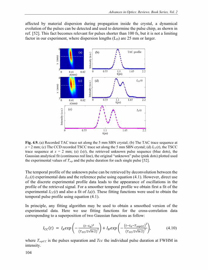
Advances in Optics: Reviews. Book Series, Vol. 2
104
affected by material dispersion during propagation inside the crystal, a dynamical evolution of the pulses can be detected and used to determine the pulse chirp, as shown in ref. [52]. This fact becomes relevant for pulses shorter than 100 fs, but it is not a limiting factor in our experiment, where dispersion lengths (LD) are 25 mm or larger.
Fig. 4.9. (a) Recorded TAC trace set along the 5 mm SBN crystal; (b) The TAC trace sequence at x = 2 mm; (c) The CCD recorded TSCC trace set along the 5 mm SBN crystal; (d) ICC(t), the TSCC trace sequence at x = 2 mm; (e) IP(t), the retrieved unknown pulse sequence (blue dots), the Gaussian analytical fit (continuous red line), the original “unknown” pulse (pink dots) plotted used the experimental values of Tsep and the pulse duration for each single pulse [52].
The temporal profile of the unknown pulse can be retrieved by deconvolution between the ICC(t) experimental data and the reference pulse using equation (4.1). However, direct use of the discrete experimental profile data leads to the appearance of oscillations in the profile of the retrieved signal. For a smoother temporal profile we obtain first a fit of the experimental ICC(t) and also a fit of IR(t). These fitting functions were used to obtain the temporal pulse profile using equation (4.1).
In principle, any fitting algorithm may be used to obtain a smoothed version of the experimental data. Here we use fitting functions for the cross-correlation data corresponding to a superposition of two Gaussian functions as follow:
/ √ / √
, (4.10)
where TsepCC is the pulses separation and Tcc the individual pulse duration at FWHM in intensity.

Chapter 4. Single-Shot Auto and Cross Correlation Schemes for Ultrashort Laser Pulse Measurement Using Random Nonlinear Crystals
105
Fig. 4.9(d) shows the fitted curve in red where Tcc = 250 fs and the temporal separation TsepCC = 299 fs. The reference pulse was fitted using a Gaussian function, with TR = 178 fs:
/ √
. (4.11)
Using these two functions and applying the deconvolution procedure, we obtained the retrieved unknown temporal pulse shown in Fig. 4.9(e) (blue dots). From the corresponding fit (red line), using the same functional form as equation (4.10), we can directly determine the unknown pulse peak separation TsepP = 299 fs, and the temporal duration of each individual Gaussian pulse, TP = 175 fs. These results are in very close agreement with the real values used in our experiment for the generation of the unknown pulse, Tsep and T.
We have generated several different double-peak pulses by setting Tsep to 200, 267, 367 and 1333 fs. Fig. 4.10 (a) shows the recorded TSCC traces along the SBN crystal for each pulse. The corresponding cross-correlation signals selected at the propagation distance x = 2 mm, are shown in Fig. 4.10 (b) together with the fitted curves (red line). The retrieved unknown temporal pulses are shown in Fig. 4.10 (c).
We estimate the error between the retrieved and set values of the unknown pulse using the following expression:
. (4.12)
The error found in the measurement shown in Fig. 4.9 war 1.9 %, while the values for the 4 different cases shown in Fig. 4.10 were 4.4 %, 1.4 %, 0.6 % and 9.9 % respectively. These results show that the longer the pulse the larger the error, but all values remain under a 10 %.
4.5. Limitations of the Technique
In the development of the technique detailed in Sections 4.3 and 4.4 we have considered the overlapping of the interacting beams without any consideration regarding the spatial extent or the bandwidth and central wavelength of the beams to be characterized. We assumed a beam with no transverse spatial dependence and a random structure that can up-convert the entire fundamental beam frequency bandwidth. In order to evaluate the possible limitations in the applicability of this technique we need to look closer at these parameters and their effect on the resulting transverse SHG signal.
The effect of the limited spatial extent of the beam is considered by assuming a more realistic model including a Gaussian spatial beam distribution also in the transverse direction as we explain in ref. [52]. The resulting auto-correlation or cross-correlation

Advances in Optics: Reviews. Book Series, Vol. 2
106
functions can be expressed as a product of two contributions: a temporal term, which is the one obtained in the plane wave approximation for the beams, and a spatial term, which dictates a change in the resulting TSHG signal imposed by the not perfect overlapping of the beams. To check the relevance of this effect in our particular configuration, we should consider the beam size, R0, relative to the pulse duration, T0. We find two extreme situations: (i) when the condition / ≪ tan / holds, the recorded transverse SH trace provides the direct mapping of the temporal pulse shape, with no limitation imposed by the finite beam size: (ii) when / ≫ tan / , the recorded correlation trace does not give a proper transverse autocorrelation function because the beam size limits the overlapping region. According to the duration of the pulses to be measured we need to consider these effects and decide the best configuration for the set-up. The angle between the beams intersecting inside the crystal becomes a crucial parameter, which we can use to control the spatial overlapping for a proper determination of the pulse duration.
Fig. 4.10. (a) Recorded TSCC traces set along the SBN crystal when Tsep are 200, 267, 367 and 1333 fs respectively; (b) TSCC profiles at the marked position in Fig. 4.10 (a); (c) retrieved
shaped pulse sequence; (d) simulated TSCC trace set along the 5-mm SBN crystal [52].

Chapter 4. Single-Shot Auto and Cross Correlation Schemes for Ultrashort Laser Pulse Measurement Using Random Nonlinear Crystals
107
The bandwidth of the pulse to be measure and the transparency range of the nonlinear crystal also imposes limits. Here we have assumed that the available reciprocal lattice vectors distribution is wide enough to provide up-conversion of our beam within the transparency window of the crystal, which for SBN occurs between 380 nm and 4 microns approximately. This values indicate that the SBN crystal will absorb those frequencies of the SH signal below 380 nm and, consequently, no perfect bandwidth conversion will be realized. This fact imposes a limitation in the pulse durations we can measure when characterizing pulses at fundamental frequencies around 800 nm, since in this case the SH signal will be centered around 400 nm and the maximum possible converted bandwidth will be of the order of 40 nm. Thus, the absorption of the crystal imposes a lower limit of 20 fs for the duration of the pulses which can be measured with this technique at fundamental wavelengths close to 800 nm. In the limit of long pulses is the spatial extent of the beams, as explained earlier, the main factor to be considered when applying this technique.
4.6. Conclusions
We have presented a review of our work related to ultrashort laser pulse characterization using the novel ideas of single-shot auto- and cross-correlation techniques. The methods are based on the utilization of the unique properties of transverse second harmonic generation originating in a crystal with random size distribution nonlinear domains. By imaging the auto-correlation trace of the SH signal emitted in the transverse direction, obtained by overlapping two non-collinear pulses, we determine pulse duration. We have implemented this procedure to pulse durations ranging between 20 fs up to 1 ps.
Unlike other, well-established auto-correlation methods, the transverse configuration enables the observation and measurement in a -shot regime of the pulse evolution during its propagation in the crystal. This measurement, together with the dispersive parameter of the crystal, allow retrieval of the initial chirp parameter. The vertical emission of TSHG removes the requirement that the nonlinear crystal be thin, and enables one to measure the undistorted pulse at the entrance of the crystal. This setup can be used for real-time monitoring of the chirp content at the measurement position. For the wavelengths corresponding to the anomalous GVD region, g < 0 (k > 2 lm for SBN), one should observe pulse compression for up-chirped pulses instead of down- chirped pulses as in the cases discussed here.
As an important characteristic, the property of automatic phase matching without angular alignment or temperature control makes the technique applicable to a broad wavelength range (limited only by the transparency window of the crystal), leading to enormous simplification of the operation process. Such type of nonlinear media can be used for nonlinear optical interactions with multiple input wavelengths or polarizations, without any further alignment or angular tuning due to available broad bandwidth provided by the random nonlinear photonic structure.
Finally, we extended our method to perform transverse cross-correlation measurements for the characterization of temporal pulse profiles of complex non-Gaussian waveforms.

Advances in Optics: Reviews. Book Series, Vol. 2
108
We measured several two-peaked Gaussian beams over a broad temporal window and studied the role played by factors such as incident angle and beam radius as error sources for the final resolution of this pulse measurement technique. We have also shown that it may be possible to perform measurements in the long pulse duration range at the expense of increased incident angle or/and expansion of the beam diameter.
Acknowledgements
C. Cojocaru and J. Trull acknowledge financial support by the Spanish Ministerio de Educación y Ciencia (projects FIS2011-29734-C02-01 and FIS2013-44174-P), by US ACQ RDECOM (projects W911NF-11-1-0387 and W911NF-12-1-0201) and Generalitat de Catalunya (2009 SGR 1168 and 2014 SGR-957). W. Krolikowski acknowledges support from the Australian Research Council and Qatar National Research Fund (NPRP8-246-1-060). Centro de Laseres Pulsados (CLPU), Salamanca, Spain, is acknowledged for graciously granting access to its facility. All authors acknowledge the collaboration of Vito Roppo, Bingxia Wang, Yan Shen and Íñigo Sola.
References
[1]. K. Oba, P. Sun, Y. Mazurenko, Y. Fainman, Femtosecond single-shot correlation system: a time-domain approach, Appl. Opt., Vol., Vol. 38, Issue 17, 1999, pp. 3810-3817.
[2]. I. Walmsley, C. Dorrer, Characterization of ultrashort electromagnetic pulses, Adv. Opt. Photonics, Vol. 1, 2009, pp. 308-437.
[3]. J. C. Diels, W. Rudolph, Ultrashort Laser Pulse Phenomena, Academic Press, San Diego, 1989.
[4]. C. Dorrer, E. M. Kosik, I. A. Walmsley, Direct space–time characterization of the electric fields of ultrashort optical pulses, Opt. Lett., Vol. 27, 2002, pp. 548-550.
[5]. Y. R. Shen, The Principles of Nonlinear Optics, Wiley, New York, 1984. [6]. R. N. Gyuzalian, S. B. Sogomonian, Z. Gy. Horvath, Background-free measurement of time
behaviour of an individual picosecond laser pulse, Opt. Commun., Vol. 29, 1979, pp. 239-242. [7]. C. Kolmeder, W. Zinth, W. Kaiser, Second harmonic beam analysis, a sensitive technique to
determine the duration of single ultrashort laser pulses, Opt. Commun., Vol. 30, 1979, pp. 453-457.
[8]. S. M. Saltiel, S. D. Savov, I. V. Tomov, L. S. Telegin, Subnanosecond pulse duration measurements by noncollinear second harmonic generation, Opt. Commun., Vol. 38, 1981, pp. 443-447.
[9]. S. M. Saltiel, S. D. Savov, I. V. Tomov, A simple technique for real time pulsewidth measurements of single ultrashort laser pulses, Opt. Quantum Electron., Vol. 14, 1982, pp. 391-394.
[10]. J. Janzsky, G. Corradi, R. N. Gyuzalian, On a possibility of analysing the temporal characteristics of short light pulses, Opt. Commun., Vol. 23, 1977, pp. 293-298.
[11]. C. Rempel, W. Rudolph, Single shot autocorrelator for femtosecond pulses, Exp. Tech. Phys., Vol. 37, Berlin, 1988, pp. 381-385.
[12]. F. Salin, P. Georges, G. Roger, A. Burn, Single-shot measurement of a 52-fs pulse, Appl. Opt., Vol. 26, 1987, pp. 4528-4531.

Chapter 4. Single-Shot Auto and Cross Correlation Schemes for Ultrashort Laser Pulse Measurement Using Random Nonlinear Crystals
109
[13]. R. Wyatt, E. Marinero, Versatile single-shot background-free pulse duration measurement technique, for pulses of subnanosecond to picosecond duration, Appl. Phys., Vol. 25, 1981, pp. 297-301.
[14]. S. Akturk, M. Kimmel, P. O’Shea, R. Trebino, Measuring pulse-front tilt in ultrashort pulses using GRENOUILLE, Opt. Express, Vol. 11, 2003, pp. 491-501.
[15]. G. Szabo, Zs. Bor, A. Miller, Phase-sensitive single-pulse autocorrelator for ultrashort laser pulses, Optics Letters, 13, 1988, pp. 746-748.
[16]. Y. Ishida, T. Yajima, A. Watanabe, A simple monitoring system for single subpicosecond laser pulses using an SH spatial autocorrelation method and a CCD image sensor, Opt. Commun., Vol. 56, 1985, pp. 57-60.
[17]. S. Saltiel, K. Stankov, P. Yankov, V. Telegin, Realization of a diffraction grating autocorrelator for single-shot ultra short light pulse measurements, Appl. Phys. B, Vol. 40, 1986, pp. 25-27.
[18]. M. Raghuramaiah, A. K. Sharma, P. A. Naik, P. D. Gupta, R. A. Ganeev, A second-order autocorrelator for single-shot measurement of femtosecond laser pulse durations, Sadhana, Vol. 26, 2001, pp. 603-611.
[19]. J. Collier, C. Danson, C. Johnson, C. Mistry, Uniaxial single shot autocorrelator, Rev. Sci. Instrum., Vol. 70, 1999, 1599.
[20]. R. Danielius, A. Stabinis, G. Valiulis, A. Varanavicius, Characterization of phase-modulated ultrashort pulses using single-shot autocorrelator, Opt. Commun., Vol. 105, 1994, pp. 67-72.
[21]. Z. Sacks, G. Mourou, R. Danielius, Adjusting pulse-front tilt and pulse duration by use of a single-shot autocorrelator, Opt. Lett., Vol. 26, 2001, pp. 462-464.
[22]. I. Walmsley, C. Dorrer, Characterization of ultrashort electromagnetic pulses, Adv. Opt. Photonics, Vol. 1, 2009, pp. 308-437.
[23]. C. Iaconis, I. A. Walmsley, Spectral phase interferometry for direct electric-field reconstruction of ultrashort optical pulses, Opt. Lett., Vol. 23, 1998, pp. 792-794.
[24]. R. Trebino, K. W. DeLong, D. N. Fittinghoff, J. N. Sweetser, M. A. Krumb€ugel, D. J. Kane, Measuring ultrashort laser pulses in the time-frequency domain using frequency-resolved optical gating, Rev. Sci. Instrum., Vol. 68, 1997, pp. 3277-3295.
[25]. J. Kane, R. Trebino, Characterization of arbitrary femtosecond pulses using frequency-resolved optical gating, IEEE J. Quantum Electron., Vol. 29, 1993, pp. 571-579.
[26]. B. Alonso, Í. J. Sola, Ó. Varela, J. Hernández-Toro, C. Méndez, J. S. Román, A. Zaïr, L. Roso, Spatiotemporal amplitude-and-phase reconstruction by Fourier-transform of interference spectra of high-complex-beams, J. Opt. Soc. Am. B, Vol. 27, 2010, pp. 933-940.
[27]. P. Bowlan, P. Gabolde, A. Shreenath, K. McGresham, R. Trebino, S.Akturk, Crossed-beam spectral interferometry: a simple, high-spectral-resolution method for completely characterizing complex ultrashort pulses in real time, Opt. Express, Vol. 14, 2006, pp. 11892-11900.
[28]. G. Berden, S. Jamison, A. MacLeod, W. Gillespie, B. Redlich, A. van der Meer, Electro-optic technique with improved time resolution for real-time, nondestructive, single-shot measurements of femtosecond electron bunch profiles, Phys. Rev. Lett., Vol. 93, 2004, 114802.
[29]. A. R. Tunyagi, M. Ulex, K. Betzler, Noncollinear optical frequency doubling in strontium barium niobate, Phys. Rev. Lett., Vol. 90, 2003, 243901.
[30]. Y. Wang, J. Ma, J. Wang, P. Yuan, G. Xie, X. Ge, F. Liu, X. Yuan, H. Zhu, L. Qian, Single-shot measurement of >10¹⁰ pulse contrast for ultra-high peak-power lasers, Sci. Rep., Vol. 4, 2014, 3818.
[31]. V. G. Dmitriev, G. G. Gurzadyan, D. N. Nikogosyan, Handbook of Nonlinear Optical Crystals, Springer, Berlin, 1991.
[32]. A. Yariv, P. Yeh, Electromagnetic propagation in periodic stratified media. II. Birefringence, phase matching, and X-ray lasers, J. Opt. Soc. Am., Vol. 67, 1977, pp. 438-447.

Advances in Optics: Reviews. Book Series, Vol. 2
110
[33]. J. A. Armstrong, et al., Interactions between lightwaves in a nonlinear dielectric, Phys. Rev., Vol. 127, 1962, pp. 1918-1939.
[34]. M. M. Fejer, G. A. Magel, D. H. Jundt, R. L. Byer, Quasi-phase-matched second harmonic generation: tuning and tolerances, IEEE J. Quantum Electron., Vol. 28, 1992, pp. 2631-2654.
[35]. J.-M. Liu, Chapter 9, in Photonic Devices, Cambridge University Press, Cambridge, 2005. [36]. M. Horowitz, A. Bekker, B. Fischer, Broadband second-harmonic generation in SrBaNb2O6
by spread spectrum phase matching with controllable domain gratings, Appl. Phys. Lett., Vol. 62, 1993, pp. 2619-2621.
[37]. J. J. Romero, C. Arago, J. A. Gonzalo, D. Jaque, J. Garcia Sole, Spectral and thermal properties of quasi-phase-matchingsecond-harmonic generation in Nd3+:Sr0.6Ba0.4 (NbO3)2 multi-self-frequency-converter nonlin- ear crystals, J. Appl. Phys., Vol. 93, pp. 3111-3113.
[38]. R. Fischer, D. N. Neshev, S. Saltiel, W. Krolikowski, Yu. S. Kivshar, Broadband femtosecond frequency doubling in random media, Appl. Phys. Lett., Vol. 89, 2006, 191105.
[39]. P. Molina, M. O. Ramirez, L. E. Bausa, Strontium Barium Niobate as a multifunctional two-dimensional nonlinear “photonic glass”, Adv. Funct. Mat., Vol. 18, 2008, pp. 709-715.
[40]. M. O. Ramirez, D. Jaque, L. Ivleva, L. E. Bausa, Evaluation of ytterbium doped strontium barium niobate as a potential tunable laser crystal in the visible, J. Appl. Phys., Vol. 95, 2004, pp. 6185-6191.
[41]. A. R. Tunyagi, M. Ulex, K. Betzler, Noncollinear optical frequency doubling in strontium barium niobate, Phys. Rev. Lett., Vol. 90, 2003, 243901.
[42]. R. Fischer, D. N. Neshev, S. M. Saltiel, A. A. Sukhorukov, W. Krolikowski, Y. S. Kivshar, Monitoring ultrashort pulses by transverse frequency doubling of counterpropagating pulses in random media, Appl. Phys. Lett., Vol. 91, 2007, 031104.
[43]. J. Janszky, G. Corradi, R. N. Gyuzalian, On a possibility of analysing the temporal characteristics of short pulses, Opt. Commum., Vol. 23, 1977, pp. 293-298.
[44]. V. Roppo, D. Dumay, J. Trull, C. Cojocaru, S. Saltiel, K. Staliunas, R. Vilaseca, D. N. Neshev, W. Krolikowski, Y. S. Kivshar, Planar second-harmonic generation with noncollinear pumps in disordered media, Opt. Express, Vol. 16, 2008, pp. 14192-14199.
[45]. J. Trull, S. Saltiel, V. Roppo, D. Dumay, W. Krolikowski, D. N. Neshev, R. Vilaseca, K. Staliunas, Y. S. Kivshar, Characterization of femtosecond pulses via transverse second-harmonic generation in random nonlinear media, Applied Physics B, Vol. 95, Issue 3, 2009, pp. 609-615.
[46]. S. M. Saltiel, S. D. Savov, I. V. Tomov, L. S. Telegin, Subnanosecond pulse duration measurements by noncollinear second harmonic generation, Opt. Commun., Vol. 38, 1981, pp. 443-447.
[47]. Y. Ishida, T. Yajima, A. Watanabe, A simple monitoring system for single subpicosecond laser pulses, Opt. Commun., Vol. 56, 1985, pp. 57-60.
[48]. J.-C. Diels, W. Rudolph, Ultrashort Laser Pulse Phenomena, 2nd Edition, Academic Press, San Diego, 2006.
[49]. Th. Woike, T. Granzow, U. Dörfler, Ch. Poetsch, W. Wöhlecke, R.Pankrath, Refractive indices of congruently melting Sr0.61Ba0.39Nb2O6, Phys. Status Solidi, Vol. 186, 2001, pp. R13-R15.
[50]. M. Nisoli, S. De Silvestri, O. Svelto, Generation of high energy 10 fs pulses by a new pulse compression technique, Appl. Phys. Lett., Vol. 68, 1996, 2793.
[51]. S. Kawai, T. Ogawa, H. S. Lee, R. C. DeMattei, R. Feigelson, Second-harmonic generation from needlelike ferroelectric domains in Sr0.6Ba0.4Nd2O6 single crystals, Appl. Phys. Lett., Vol. 73, 1998, 768.
[52]. J. Trull, I. Sola, B. Wang, A. Parra, W. Krolikowski, Y. Sheng, R. Vilaseca, C. Cojocaru, Ultrashort pulse chirp measurement via transverse second-harmonic generation in strontium barium niobate crystal, Appl. Phys. Lett., Vol. 106, 2015, 221108.

Chapter 4. Single-Shot Auto and Cross Correlation Schemes for Ultrashort Laser Pulse Measurement Using Random Nonlinear Crystals
111
[53]. B. Wang, C. Cojocaru, W. Krolikowski, Y. Sheng, J. Trull, Transverse single-shot cross-correlation scheme for laser pulse temporal measurement via planar second harmonic generation, Optics Express, Vol. 24, Issue 19, 2016, 22210.


Chapter 5. Modeling the Interaction of Laser Beams with Plasma by using the FDTD Method
113
Chapter 5 Modeling the Interaction of Laser Beams with Plasma by using the FDTD Method
Zhili Lin1
5.1. Introduction
Plasma is one of the four fundamental states of matter and the unique interaction of light with plasma is an interesting phenomenon. When the laser power is less than 2 21 W1 /cm0 , the dispersive and dissipative permittivity of plasma is often described by the conventional linear Drude model [1]. However, with the development of high-power laser technology, the pulsed laser beams can be focused with extremely high intensity of the order of
0 22 W1 /cm0 . Thus in the past several decades, the complex interaction of high-power laser beams with plasma has been a subject of great interest for worldwide physicists since it is relevant for various important physical applications [2-4]. In the presence of high-power laser beams, the spatial inhomogeneity of light intensity can exert the ponderomotive force on electrons. When the ponderomotive force applied to the electrons is comparable to the electron pressure gradient force, a significant nonlinear effect appears that is sensitive to the radiance distribution of laser beam [5, 6]. So far the main thrust of theoretical investigations have been directed to the study of nonlinear propagation characteristics of various types of laser beams that leads to the self-focusing phenomena in plasma [7-10]. However, the main research methods they usually used are to analytically solve the various scalar wave equations corresponding to different types of incident laser beams and the paraxial approximations are often applied to reduce the calculation complexity. Therefore, the obtained information about the vector nature of light fields of laser beams is limited and not so accurate for the case of a small focused beam with size in the order of several wavelengths and with a large diffraction effect. Fortunately, with the rapid progress of computer hardware, the finite-difference time-domain (FDTD) method has become one of the most powerful numerical techniques in directly solving the Maxwell’s curl equations [11] and has been widely applied to model and solve optics and photonics problems [12]. In literature, the FDTD method is often applied to model the linear Drude model of plasma by using the popular FDTD approaches
Z. Lin Fujian Key Laboratory of Light Propagation and Transformation, College of Information Science and Engineering, Huaqiao University, Xiamen, China

Advances in Optics: Reviews. Book Series, Vol. 2
114
for dispersive media, such as the auxiliary differential equation (ADE) approach [13], the bilinear-transform (BT) approach [14], the Z-transform (ZT) approach [15], the piecewise linear recursive convolution (PLRC) approach [16] and the Maclaurin series expansion (MSE) approach [17]. In this chapter, we try to simulate the conventional linear Drude model by the BT approach and simulate the modified nonlinear Drude model by the MSE approach together with the composite trapezoidal rule for extracting the time average of the square of light field. We also introduce the powerful total-field/scattered-field (TF/SF) technique [18] to generate the various types of laser beams based on the well-known equivalence principle [19]. Three numerical examples, corresponding to two different power levels of Gaussian laser beams and a high-power vortex Laguerre-Gaussian beam, propagating in collisional plasma, are presented under the specified laser and plasma parameters to verify the effectiveness of the proposed FDTD-based techniques. The simulation results show the anticipated self-focusing and attenuation phenomena of laser beams and the deformation of the spatial density distributions of electron plasma along the beam propagation path. Due to the flexibility of FDTD method in laser beam excitation, the proposed techniques have a wide application prospect in the study of complex laser-plasma interaction.
5.2. Physical Models of Plasma
5.2.1. Linear Drude Model
When the light intensity of laser beam is not so high, the interaction of laser beam with plasma is linear and the permittivity of plasma can be described by the conventional linear Drude model [1]. As a matter of fact, according to the conservation of mass and momentum theorem and the continuity equation of charge current, we can deduce that the electric polarization intensity of non-magnetized plasma is
0 P E (5.1)
with the electric susceptibility given by
2p
c
,( j )
(5.2)
where represents ions or electrons and c is the collision frequency. Then, we obtain
the effective dielectric constant
2p
rc
1 1 .( j )
(5.3)
As the heavy ions are often taken fixed due to their large mass, the dispersive characteristics of plasma is mostly determined by the electrons, so that the expression can be simplified to

Chapter 5. Modeling the Interaction of Laser Beams with Plasma by using the FDTD Method
115
2pe
r ec
1 1 1 ,( j )
(5.4)
where pe is the electron resonant frequency given by
2
epe
0 e
n e
m
(5.5)
with en the electron density, e the elementary charge and
em the rest mass of electron. Eq. (5.4) is the so-called linear Drude model, which is often used to explain the transport properties of electrons in metals.
5.2.2. Nonlinear Drude Model
However, when the light intensity of laser beam is extremely high, the interaction of laser beam with plasma become a nonlinear process [20]. The charged particles would experience a nonlinear Lorentz force called the ponderomotive force [21] in the inhomogeneous oscillating electromagnetic fields of high-power laser beams. Since the ponderomotive force is inversely proportional to the mass of particle, the ponderomotive effect on ions is generally negligible with respect to that on free electrons. Thus such a nonlinear force redistribute the electron density in plasma until the balance is restored with the plasma pressure gradient force. For the normal incidence of laser beam on plasma,
the ponderomotive force per unit volume, pf is determined proportionally by the gradient
of light field intensity,
2
2ep 2
e L
( )( , ) ,
2
n eE t
m
r
f r (5.6)
where L is the angular frequency of laser beam,
e ( )n r is the space-dependent electron
density. 2 ( , )E tr is the time average of the square of light field over one oscillating
period. On the other hand, the plasma pressure gradient force per unit volume, pgf is
correlated with the electron temperature of plasma and the gradient of electron density,
pg B e e( ),k T n f r (5.7)
where Bk is the Boltzmann's constant and
eT is the electron temperature given in kelvin and often taken to be constant for a pulsed laser beam incidence. In the steady state with equilibrium, the ponderomotive force balances with the pressure gradient force,
2
2B e2
e L
( )( , ) ( ).
2
n eE t k T n
m
r
r r (5.8)

Advances in Optics: Reviews. Book Series, Vol. 2
116
By integrating Eq. (5.8) from 0n to n, we obtain the expression for the electron density,
2 2
0 2e B e L
( , )( ) ( )exp ,
2
e E tn n
m k T
rr r (5.9)
where 0 ( )n r is the initial electron density prior to the incidence of laser beam. Moreover,
one has the space-dependent dispersive dielectric constant model of collisional plasma
2pe
r 2c
( )( , ) 1 ,
i
r
r (5.10)
where 2pe e 0 e( ) ( ) /e n m r r is the space-dependent plasma (electron) resonance
frequency. Consequently, the nonlinear, dispersive and dissipative dielectric constant function of plasma takes the form [22]
2p0 2
r 2c
( )( , ) 1 exp ( , ) ,E t
i
r
r r (5.11)
where 2 2e B e L/ ( 2 )e m k T is the exponential coefficient and p0 0 0 e( ) ( ) /e n m r r is
the initial plasma resonance frequency. It is noted that the permittivity is dependent on the
quantity 2 ( , )E tr , the light intensity of laser beam, from which the nonlinear phenomena
ensue, such as the self-focusing of laser beams [22, 23]. When the laser power is low, the exponential item in Eq. (5.11) approaches unit one and the nonlinear Drude model given by Eq. (5.11) reduces to the linear Drude model given by Eq. (5.4).
5.3. FDTD Implementations of Models
5.3.1. Implementation of Linear Drude Model
First we try to implement the linear Drude model of plasm when the light power of the incident laser beam is low [24]. The corresponding constitutive relation of plasma corresponding to the linear Drude model given by Eq. (5.4) can be rewritten as
2pe
0 2c
1 .( j ) ( j )
D E (5.12)
As previously mentioned in the introduction section, there are many approaches can be utilized to implement Eq. (5.12) in the framework of FDTD method. Here, one of the most accurate approaches, the bilinear transform (BT) approach, is utilized as the application example. First, we define the auxiliary quantity

Chapter 5. Modeling the Interaction of Laser Beams with Plasma by using the FDTD Method
117
2 2pe p
2 2c c
• • ,(j ) ( j ) ( )( j ) ( )t t j t
S E E (5.13)
so
0( ) ( ) ( ) . D E S (5.14)
By applying the bilinear transformation based on the substitution formula
1
1
1j 2
1
Zt
Z
(5.15)
with je tZ , we have the discrete time-domain relationship between S and E ,
2
pe
1 12
c 1 1
.1 1
2 (2 )1 1
n nt
Z Zt
Z Z
S E (5.16)
Noting that 1 1•n nZ E E and 1 1•n nZ S S , one has the updating equation
1 2 1 21 2 3( 2 ) ,n n n n n nC C C S E E E S S (5.17)
is obtained, where the coefficients 21 p c/ ( 2 4 )C ,
2 c4 / ( 2 )C and
3 c c( 2 ) / ( 2 )C with the normalized parameters 2 2 2p p e t and c c t . By
substituting Eq. (5.11) into Eq. (5.8), we finally obtain the updating equation for E ,
1 2 1 20 1 2 3
1
1[ / (2 ) ].
1n n n n n nC C C
C
E D E E S S (5.18)
5.3.2. Implementation of Nonlinear Drude Model
We move on to implement the nonlinear Drude model described by Eq. (5.11) by using the FDTD method [25]. In this case, the Maclaurin series expansion (MSE) approach is applied to model the dispersive constitutive relationship [17] and we have
2 21 1
1 p0 1 2 p0 21 10 1 22 2 2
0 0 p0 0 0 p0 0 0 p0 0
,( )
n n nn n n
a b a bb b b
a b a b a b
D D DE E E (5.19)
where the normalized parameter 2 2 2 2p0 p0 exp ( , )t E t r and the dimensionless
coefficients 20 c c6 3a , 2
1 c6 0 4a , 22 c c 6 3a , 3
0 c c7 2 3 6 3b ,
1 144b and 32 c c7 2 3 6 3b . It should be noted that
2p0 is dependent on the time

Advances in Optics: Reviews. Book Series, Vol. 2
118
average of the square of light field 2( , )E tr . So here the difficulty is how to extract
2( , )E tr in the discrete framework of FDTD algorithm. In fact, for the FDTD method
with spatially interlaced Yee cells, the square of light field 2 ( , )E tr can be approximately
and averagely evaluated at the center of the , , i j k th cubic Yee cell by
2 2 2 2 2( , ) ( , ) ( , ) ( , ) ( , ),x y zE t E t E t E t E t r r r r r (5.20)
where
1 1 1
( ) ( ) ( ) ,2 2 2x y zi x j y k z r e e e (5.21)
1 1[ , , , ] [ , 1, , ]
1 2 2( , ) ,1 14
[ , , 1, ] [ , 1, 1, ]2 2
x x
x
x x
E i j k t E i j k tE t
E i j k t E i j k t
r (5.22)
1 1[ , , , ] [ 1, , , ]
1 2 2( , ) ,1 14
[ , , 1, ] [ 1, , 1, ]2 2
y y
y
y y
E i j k t E i j k tE t
E i j k t E i j k t
r (5.23)
1 1[ , , , ] [ 1, , , ]
1 2 2( , ) ,1 14
[ , 1, , ] [ 1, 1, , ]2 2
z z
z
z z
E i j k t E i j k tE t
E i j k t E i j k t
r (5.24)
where , ,x y z are omitted in Eqs. (5.22-5.24) for compactness. Note that regardless of the polarization state of laser beam with oscillating light field, the time average of the square of light field over one oscillating period is equal to that over one-half period,. Thus
2( , )E tr can be calculated and updated in the interval of half period by [25]
0 L 0 L
0 0
/ 22 2 2
L L
1 2( , ) ( , )d ( , )d ,
t T t T
t tE t E t t E t t
T T
r r r (5.25)
where L L2 π /T is the oscillating period and
0t is the initial time instant of integration. By applying the composite trapezoidal rule to calculate the half-period definite integral in Eq. (5.25), one obtains
1
2 2 2 2
/2 1
1( , ) [ , ( ) ] ( , ) 2 ( , )
2T
nT
m n NT
NE t E n t E n t E m t
N
r r r r (5.26)

Chapter 5. Modeling the Interaction of Laser Beams with Plasma by using the FDTD Method
119
in the time interval [( ) , ]2
TNn t n t , where
L /TN T t is the number of time steps
per period and is usually an even integer. If the spatial discretization number L /N x
and the stability number CFL /n s c t are defined, one has
CFLTN n N . Here, TN is
preferred an even integer because it can be demonstrated [26] that the relative error of
Eq. (5.26) in numerically calculating 2( , )E tr as compared with its analytical
counterpart 2( , )E tr determined by Eq. (5.25) diminished.
5.4. Numerical Laser Beam Generation
The FDTD numerical technique for the generation of laser beams with specified patterns and parameters is another important aspect in view of the study of laser-plasma interaction [24]. Without loss of generality, consider that the to-be-generated laser beam is associated with the electromagnetic fields,
L ( , , , )x y z tE andL ( , , , )x y z tH , which are dependent both
on time and space. The total field/scattering field (TF/SF) source condition popular for generating plane waves in FDTD method is applied here. According to the staggered structure of YEE cells, assume that the TF/SF interface is perpendicular to the z axis and locates at
s( 1 / 4 )z k z , then the tangential components of the total electric field on
the grid plane sz k z at the time instant ( 1)t n t can be updated by
( 1) ( 1) ( 1/2)t, s t, s FDTD L, s
1 1 1 1( , , ) ( , , ) ( , , ),
2 2 2 2n n nx x y
tD i j k D i j k H i j k
z
(5.27)
where ( 1/2)L,nyH
is the y component of magnetic field of the to-be-excited laser beam,
( 1/2)L, s L, s
1 1 1 1 1( , , ) [( ) , , ( ) , ( ) ],
2 2 2 2 2ny yH i j k H i x j y k z n t (5.28)
on the grid plane s( 1 / 2)z k z , and
( 1) ( 1) ( 1/2)t, s t, s FDTD L, s
1 1 1 1( , , ) ( , , ) ( , , ),
2 2 2 2n n ny y x
tD i j k D i j k H i j k
z
(5.29)
where ( 1/2)L,nxH
represents the x component of the magnetic field of the to-be-excited
laser beam,
( 1/2)L, s L, s
1 1 1 1 1( , , ) [ , ( ) , ( ) , ( ) ],
2 2 2 2 2nx xH i j k H i x j y k z n t (5.30)
on the grid plane s( 1 / 2)z k z . On the other hand, the tangential components for the
scattering magnetic field on the grid plane s( 1 / 2)z k z at the time instant
( 1 / 2)t n t should be updated by

Advances in Optics: Reviews. Book Series, Vol. 2
120
( 1/2) ( 1/2) ( )s, s s, s FDTD L, s
1 1 1 1 1( , , ) ( , , ) ( , , ),
2 2 2 2 2n n nx x y
tB i j k B i j k E i j k
z
(5.31)
where ( )L,
nyE represents the y component of the electric field of the laser beam,
( )L, s L, s
1 1( , , ) [ , ( ) , , ],
2 2ny yE i j k E i x j y k z n t (5.32)
on the grid plane sz k z , and
( 1/2) ( 1/2) ( )s, s s, s FDTD L, s
1 1 1 1 1( , , ) ( , , ) ( , , ),
2 2 2 2 2n n ny y x
tB i j k B i j k E i j k
z
(5.33)
where ( )L ,
nxE is the x component of the electric field of the incident laser beam,
( )L, s L, s
1 1( , , ) [ , ( ) , , ],
2 2ny yE i j k E i x j y k z n t (5.34)
on the grid plane sz k z . For example, consider to generate a basic Gaussian laser
beam with electric field given by
2 2
0L 0 02( , , , ) exp sin ( ) ,
( ) 2 ( )( )
w r rx y z t E t k z z z
w z R zw z
E e (5.35)
where 2 /k is the wave number, 0E is the magnitude of the electric field in the
center of the beam waist, 0w is the waist size of Gaussian laser beam at
0z z ,
0
2 20( ) 1 ( ) / Rw z w z z z is the waist size of Gaussian laser beam with the Rayleigh
length 2
R 0 /z w , 2
0 R 0( ) ( )1 [ /( )] R z z z z z z is the radius of curvature of the
beam's wavefront, and 0 R( ) arc tan[( ) / ]z z z z is the Gouy phase. With the analytical
expression for the electric field of laser beam given by Eq. (5.35), the corresponding magnetic field can be analytically derived or numerically calculated by the Faraday's law of electromagnetic induction
L L
1( , , , ) ( , , , ) d .x y z t x y z t t
H E (5.36)
From Eqs. (5.35) and (5.36), we obtain the needed discrete data of light fields on the corresponding boundary planes that are ready to be used in Eqs. (5.27), (5.29), (5.31) and (5.33), respectively. This preparing process can be performed prior to the FDTD simulations.

Chapter 5. Modeling the Interaction of Laser Beams with Plasma by using the FDTD Method
121
5.5. Numerical Examples and Results
5.5.1. Low-power Gaussian Laser Beam
The first example goes to investigate the propagation characteristics of a Gaussian laser beam in collisional plasma [24]. The designed simulation configuration is shown in Fig. 5.1.
Fig. 5.1. Configuration of FDTD simulation for Gaussian laser beam propagation in collisional plasma. Adapted from: Z. Lin, Proc. SPIE, Vol. 10016, 2016, pp. 100160W, © 2016 SPIE.
The computation region is bounded by 10-cell perfectly matched layers (PMLs) [27] and filled by homogeneous plasma with the electron density
e ec1 / 3n n , where the critical
density is 2 7 3ec 9 .0 5 7 2 1 0 /mn and the collision frequency is c pe0.03 are
assumed. The y-polarized Gaussian laser beam with a maximum amplitude5
0 1 10 V/myE on the central waist plane is generated by using the TF/SF source
condition and horizontally propagates in the homogeneous plasma to the right side. The discrete size of Yee cell is /12 and the time step is / 2t x c , where c is the speed of light in vacuum. Fig. 5.2 shows the simulation results for the spatial distributions of the
electric field yE and light intensity I . It is noted that the gradual attenuation of the laser
intensity is apparent due to the absorption of laser energy by the plasma through the process of electron acceleration and the collision between electrons and heavy ions.
5.5.2. High-power Gaussian Laser Beam
The second example is configured for simulating the propagation of a high-power Gaussian beam in collisional plasma where the effect of ponderomotive force is taken into consideration [25]. In the 3D-FDTD simulation, the Gaussian beam generated by the TF/SF source condition is with the parameters
L 351 nm , 1 00 2 1 0 V /mE and
0 L2w , and the plasma is with the parameters 2 7 30 3 1 0 / mn , 4
e 1 10 KT and

Advances in Optics: Reviews. Book Series, Vol. 2
122
c p00.01 . The total sizes of the computation region is 200200440 cells including
the surrounding 20-cells-thick PMLs [27] to completely absorb the outgoing light waves. The spatial and temporal discretization parameters are 2 0N and
CFL 2n , so that
4 0TN . The simulation results are shown in Fig. 5.3 and Fig. 5.4. The longitudinal-
section views of the spatial distributions of transient field component xE and the light-
field magnitude of laser beam normalized to 0E and propagating in free space and in
plasma over the xOz planes are illustrated in Figs. 5.3(a)-(b) and Figs. 5.3(d)-(e), respectively. The spatial distribution of plasma density normalized to
0n over the xOz plane is also shown in Fig. 5.3(f), which is determined by Eq. (5.4) with the extracted
values of 2( , )E tr . It is noted that the Gaussian laser beam is focused in the plasma and
the plasma density distribution is deformed by the ponderomotive force from its initial uniform distribution with a penetration length approximately
L12 . Fig. 5.4 shows the cross-sectional slices of the spatial distributions of light-field magnitudes normalized to
0E in the collisional plasma on the several specified cross-sectional planes. The light fields are with stochastic distributions on the cross-sectional planes along the propagating direction while the light energy is gradually absorbed by the plasma.
Fig. 5.2. Simulation results for the spatial distributions of (a) the electric field ( , , )yE x z t and (b)
light intensity ( , )I x z for the low-power Gaussian laser beam propagation in plasma with the linear
Drude model. Source: Z. Lin, Proc. SPIE, Vol. 10016, 2016, pp. 100160W, © 2016 SPIE.

Chapter 5. Modeling the Interaction of Laser Beams with Plasma by using the FDTD Method
123
Fig. 5.3. The longitudinal-section views of the simulation results of the second numerical example. (a) The transient distribution of field component xE of Gaussian beam in free space (a) and in
plasma (d) over the xOz plane; the normalized distribution of light field magnitude in free space (b) and in plasma (e); (c) free space without plasma; (f) the normalized density profile of plasma deformed by the ponderomotive force. Source: Z. Lin, X. Chen, P. Ding, W. Qiu, and J. Pu, Optics Express, Vol. 25, 2017, pp.8440-8449, ©2017 OSA.
Fig. 5.4. The spatial distribution of light field magnitude of Gaussian laser beam in plasma on the several cross-section planes specified by the different z values where L 20 z . Source: Z. Lin,
X. Chen, P. Ding, W. Qiu, and J. Pu, Optics Express, Vol. 25, 2017, pp.8440-8449, ©2017 OSA.

Advances in Optics: Reviews. Book Series, Vol. 2
124
5.5.3. High-power Vortex Laguerre-Gaussian Laser Beam
The third numerical example is designed for investigating the ponderomotive interaction of a vortex Laguerre-Gaussian (vLG) beam with collisional plasma [25]. The boundary light field of the vortex Laguerre-Gaussian beam can be expressed in cylindrical coordinates ( , , z) with the complex form [28]
2
0 20 0
2( , 0) exp exp(i ),
m
xz E mw w
E e (5.37)
where 0E and
0w are the characteristic amplitude and beam size, m is the topological
charge of the vortex beam that determines its orbital angular momentum ( m). In this simulation, the discretization parameters and the parameters of vLG beam and plasma are the same as the second example except that
0 L1 .5w and 2m . Different initial phases are assigned to the various grids on the source plane according to Eq. (5.37). The simulation results of the spatial distributions of light fields and plasma density over the xOz plane are illustrated in Fig. 5.5 and Fig. 5.6.
Fig. 5.5. The longitudinal-section views of the simulation results of the third numerical example. (a) The transient distribution of field component xE of vLG laser beam in free space (a) and in
plasma (d) over the xOz plane; the normalized distribution of light field magnitude in free space (b) and in plasma (e); (c) free space without plasma; (f) the normalized density profile of plasma deformed by the ponderomotive force. Source: Z. Lin, X. Chen, P. Ding, W. Qiu, and J. Pu, Optics Express, Vol. 25, 2017, pp. 8440-8449, ©2017 OSA.

Chapter 5. Modeling the Interaction of Laser Beams with Plasma by using the FDTD Method
125
Fig. 5.6. The spatial distribution of light field magnitude of vLG laser beam in plasma on several cross-section planes specified by the different z values where L 20 z . Source: Z. Lin, X. Chen,
P. Ding, W. Qiu, and J. Pu, Optics Express, Vol. 25, 2017, pp. 8440-8449, ©2017 OSA.
The longitudinal-section views of the spatial distributions of transient field component xE
and the light-field magnitudes of laser beams normalized to 0E and propagating in free
space and in plasma over the xOz planes are illustrated in Figs. 5.5 (a)-(b) and Figs. 5.5 (d)-(e), respectively. The spatial distribution of plasma density normalized to
0n
over the xOz plane is also shown in Fig. 5.5 (f). Fig. 5.6 shows the cross-sectional views of the spatial distributions of light-field magnitudes of laser beam normalized to
0E in the collisional plasma on the several cross-section planes. It is noted that the rotation of electron plasma and self-focusing phenomenon is manifested that makes the width of laser ring thinner and resists the diffraction effect of laser beam. Due to the vortex of laser beam, the penetration depths of laser ring at four azimuthal angles are found longer than that of others, such as the one illustrated in Fig. 5.5 (f) where the upper branch with 0 has
more strong penetrating power.
5.6. Conclusions
In this Chapter, the FDTD method and the relevant numerical techniques are applied to modeling the complex interaction of both low-power and high-power laser beams with collisional plasma described by the linear and the modified nonlinear Drude model. The linear Drude model is implemented by the bilinear transform (BT) approach. The nonlinear Drude model is implemented by the Maclaurin series expansion (MSE) approach together with the composite trapezoidal rule to extract the time average of the square of light field. The FDTD formulation for the generation of the various types of

Advances in Optics: Reviews. Book Series, Vol. 2
126
laser beams are also presented according to the full utilization of the TF/SF source condition. Three typical numerical examples of low-power and high-power laser beam propagation in plasma are presented. The obtained numerical results show the gradual attenuation of laser intensity due to the absorption of laser energy by the plasma. For high-power laser beams, the anticipated self-focusing and attenuation phenomena and the deformation of the spatial density distributions of electron plasma along the beam propagation path are demonstrated. Since the FDTD method is flexible in the laser beam excitation, the complex interaction of various laser beams with plasma can be accurately simulated. The discussed techniques have a wide application prospect in the study of the laser-plasma interaction in a scale from several to hundreds of wavelengths.
Acknowledgements
This work was supported by the National Science Foundation of China (61101007), the Fujian Province Science Fund for Distinguished Young Scholars (2015J06015), the Program for New Century Excellent Talents of Fujian Provincial Universities, the Incubation Program for Outstanding Young Researchers of Fujian Provincial Universities (JA14011) and the Promotion Program for Young and Middle-Aged Teachers in Science and Technology Research of Huaqiao University (ZQN-YX203).
References
[1]. P. Drude, Zur Elektronentheorie der Metalle; II. Teil. Galvanomagnetische und thermomagnetische Effecte, Annalen der Physik, Vol. 308, Issue 11, 1900, pp. 369-402.
[2]. J. D. Lindl, P. Amendt, R. I. Berger, S. G. Glendinning, S. H. Glenzer, S. W. Haan, R. L. Kauffman, O. L. Landen, L. J. Suter, The physics basis for ignition using indirect-drive targets on the National Ignition Facility, Phys. Plasmas, Vol. 11, Issue 2, 2004, pp. 339-491.
[3]. S. Suckewer, C. H. Skinner, Soft x-ray lasers and their applications, Science, Vol. 247, 1990, pp. 1553-1557.
[4]. E. Esarey, P. Sprangle, J. Krall, A. Ting, Overview of plasma based accelerator concepts, IEEE Trans. Plasma. Sci., Vol. 24, Issue 2, 1996, pp. 252-288.
[5]. N. S. Saini, T. S. Gill, Self-focusing and self-phase modulation of an elliptic Gaussian laser beam in collisionless magneto plasma, Laser Part. Beams, Vol. 24, Issue 3, 2006, pp. 447-453.
[6]. M. S. Sodha, S. K. Mishra, S. Misra, Focusing of dark hollow Gaussian electro-magnetic beams in a plasma, Laser Part. Beams, Vol. 27, Issue 1, 2009, pp. 57-68.
[7]. M. V. Takale, S. T. Navare, S. D. Patil, V. J. Fulari, M. B. Dongare, Self-focusing and defocusing of TEM0p Hermite-Gaussian laser beams in collisionless plasma, Opt. Commun., Vol. 282, 2009, pp. 3157-3162.
[8]. Thakur, J. Berakdar, Self-focusing and defocusing of twisted light in non-linear media, Opt. Express, Vol. 18, Issue 26, 2010, pp. 27691-27696.
[9]. Y. Wang, C. Yuan, Z. Zhou, L. Li, Y. Du, Propagation of Gaussian laser Beam in cold plasma of Drude model, Phys. Plasma, Vol. 18, Issue 11, 2011, p. 113105-6.
[10]. R. Niknam, N. Akhlaghipour, Microwave ponderomotive action on the inhomogeneous collisioless and collisional plasma, Waves in Radom and Complex Media, Vol. 23, Issue 2, 2013, pp. 189-199.

Chapter 5. Modeling the Interaction of Laser Beams with Plasma by using the FDTD Method
127
[11]. A. Taflove, S. C. Hagness, Computational Electrodynamics: The Finite Difference Time Domain Method, Artech House, 3rd ed., 2005.
[12]. A. Taflove, A. Oskooi, S. G. Johnson, Advances in FDTD Computational Electrodynamics: Photonics and Nanotechnology, Artech House, 2013.
[13]. M. Okoniewski, M. Mrozowski, M. A. Stuchly, Simple treatment of multi-term dispersion in FDTD, IEEE Microw. Guided Wave Lett., Vol. 7, Issue 5, 1997, pp. 121-123.
[14]. C. Hulse, A. Knoesen, Dispersive models for the finite-difference time-domain method: Design, analysis, and implementation, J. Opt. Soc. Amer. A, Vol. 11, Issue 6, 1994, pp. 1802-1811.
[15]. D. M. Sullivan, Frequency-dependent FDTD methods using Z transforms, IEEE Trans. Antenna Propagat., Vol. 40, Issue 10, 1996, pp. 1223-1230.
[16]. D. F. Kelley, R. J. Luebbers, Piecewise linear recursive convolution for dispersive media using FDTD, IEEE Trans. Antennas Propagat., Vol. 44, Issue 6, 1996, pp. 792-797.
[17]. Z. Lin, C. Zhang, P. Ou, Y. Jia, L. Feng, A generally optimized FDTD model for simulating arbitrary dispersion based on the Maclaurin series expansion, J. Lightwave Technol., Vol. 28, Issue 19, 2010, pp. 2843-2850.
[18]. T. Tan, M. Potter, FDTD discrete planewave (FDTD-DPW) formulation for a perfectly matched source in TFSF simulations, IEEE Trans. Antenna Propagat., Vol. 58, Issue 8, 2010, pp. 2641-2648.
[19]. D. E. Merewether, R. Fisher, F. W. Smith, On implementing a numeric Huygen’s source scheme in a finite difference program to illuminate scattering bodies, IEEE Trans. Nucl. Sci., Vol. 27, Issue 6, 1980, pp. 1829-1833.
[20]. W. L. Kruer, The Physics of Laser Plasma Interactions, Westview Press, 2003. [21]. S. Eliezer, The Interaction of High-Power Lasers with Plasmas, IOP Press, 2002. [22]. N. Kant, S. Saralch, H. Singh, Ponderomotive self-focusing of a short laser pulse under a
plasma density ramp, Nukleonika, Vol. 56, Issue 2, 2011, pp. 149-153. [23]. N. Kant, M. A. Wani, A. Kumar, Self-focusing of Hermite-Gaussian laser beams in plasma
under plasma density ramp, Opt. Commun., Vol. 285, 2012, pp. 4483-4487. [24]. Z. Lin, Interaction of high power laser beams with plasma in ICF hohlraum using the FDTD
method, Proc. SPIE 10016, High-Power Lasers and Applications VIII, 2016, pp. 100160W. [25]. Z. Lin, X. Chen, P. Ding, W. Qiu, J. Pu, Modeling the ponderomotive interaction of high-
power laser beams with collisional plasma: the FDTD-based approach, Opt. Express, Vol. 25, Issue 7, 2017, pp. 8440-8449.
[26]. S. C. Chapra, R. P. Canale, Numerical Methods for Engineers, McGraw-Hill, 6th ed., 2010. [27]. J. Roden, S. Gedney, Convolution PML (CPML): an efficient FDTD implementation of the
CFS-PML for arbitrary media, Microw. Opt. Tech. Lett., Vol. 27, Issue 5, 2000, pp. 334-339. [28]. D. M. Palacios, I. D. Maleev, A. S. Marathay, G. A. Swartzlander, Spatial correlation
singularity of a vortex field, Phys. Rev. Lett., Vol. 92, Issue 14, 2004, p. 143905-4.


Chapter 6. Laser Separation and Recovery of Rare Earth Elements from Coal Ashes
129
Chapter 6 Laser Separation and Recovery of Rare Earth Elements from Coal Ashes
Tran X. Phuoc, Ping Wang and Bret H. Howard1
6.1. Introduction
Strategic minerals and rare earth elements are very important components in many technologies such as cell-phones, semiconductors, permanent magnets, wind turbines, etc. Traditionally, these valuable materials are extracted from natural mineral sources. Recently, however, it has been realized that, among many common elements, coal ash also contains rare earth elements whose concentrations could be enriched up to within the range of mineral ore deposits [1, 2].
Generally, steps, which include initial acid leaching of ash materials, followed by material removal, separation, and purification are used to separate rare earth elements from coal ashes [2]. Since these separation steps use large amount of water, leaching acids, caustic precipitates and organic solvents, they generate significant waste streams that are potentially toxic and must be properly disposed of. For these reasons, there is a need for a safer, more environmentally friendly approach for rare earth recovery from coal ash.
6.2. Laser Radiation Forces
Since a photon carries both energy and momentum, when it interacts with a particle, photon-particle energy and momentum transfer occur resulting in mechanical forces acting on the particle. If the particle is absorptive, the energy transfer is significant, the particle is heated and a temperature gradient forms on its surface. In this case, the force is categorized as the photophoretic force due to the surrounding gas molecules that rebound off the particle surface at different velocities depending on the surface temperature at the impact site. If the particle is non-absorptive or weakly absorbs the photon, the momentum transfer during refraction and reflection of the photon becomes dominant. In this case, the
Tran X. Phuoc National Energy Technology Laboratory (NETL), U.S. Department of Energy, USA

Advances in Optics: Reviews. Book Series, Vol. 2
130
resulting force is called the photon pressure force which has been studied for particle trapping, manipulations, separation, and levitation [3-23].
The photon force described above has been modeled using the wave optics [3-6] for particles sizes smaller than the laser wavelength. When the particle size is much larger than the laser wavelength, however, the photon pressure force can be determined by ray optics [7-15]. In this case, we consider the interaction between a particle and a loosely focused laser beam as shown in Fig. 6.1. The particle has the complex refractive index m2 = N2 – ik2, (N2 is the particle refractive index, k2 is the extinction coefficient) and it is illuminated by a Gaussian laser beam. The particle is located at a distance x from the beam waist. A light beam following ray OA reaches the particle at point A. At A, the beam partly reflects following ray AR and the rest will be absorbed and transmitted through the particle via multiple reflected rays A1, 12, 23… and multiple transmission beams 1T1, 2T2, 3T3, 4T4, etc.
Fig. 6.1. Geometrical representation of the ray-optics model for developing the force equations (d is the beam diameter, a is the particle radius, f is the focal length, wo is the beam waist, w is the beam width, r is the beam radius h is the distance from the particle to the beam center, x is the location of the particle in the x-direction, y is the vertical directionα is the beam divergent angle, βR is the reflection angle of AR, βT is the angle makes by the transmission beam with x-direction, and θ, θ1, and θ2 are angles, [23]).
Let pOA, pAR, pA1, p12, p23, p1T, p2T, p3T be the photon momentum of ray OA, AR, A1, 12, 23…, respectively, the photon momentum exchanges at A, 1, 2, 3… (1, 2, 3…N are the locations at which the ray is internally reflected and transmitted through the particle) are

Chapter 6. Laser Separation and Recovery of Rare Earth Elements from Coal Ashes
131
.
,
,
,
343233
232122
12111
1
pppdp
pppdp
pppdp
pppdp
T
T
TA
AAROAA
(6.1)
If dF is the force acting on the particle due to ray OA, according to Newton’s law it is calculated as
.1
NnA
dt
dp
dt
dp
dt
dpdF (6.2)
From Eq. (6.1) the force dF becomes
.1
,,, N
nTnARAOAA pppdFdt (6.3)
The x components of the force, defined as the force following the beam direction, is
.coscoscos1
,,, N
TnTnRARAOAAx pppdtdF (6.4)
The y component of the force in the direction perpendicular to the laser beam is
.sinsinsin1
,,, N
TnTnRARAOAAy pppdtdF (6.5)
Since the curvature of the wave of a loosely focused laser beam can be negligible [11, 12], the photon streams are assumed to travel in the direction parallel to the laser propagation direction. Thus, by letting α = 0, we obtain the following results
,1 (6.6)
,sinsin 2211 NN (6.7)
,cos2 2 a (6.8)
,2 1 R (6.9)
,,...5,3,1;22 1 nnnT (6.10)
,,...6,4,2;22 1 nnnT (6.11)
and the axial and the radial components of the force become

Advances in Optics: Reviews. Book Series, Vol. 2
132
, , 1 , 2 11
cos 2 1 cos 2 ,N
n
x A OA A AR n nTdF dt p p p n (6.12)
, 1 , 2 11
sin 2 1 sin 2 2 .N
n
y A AR n nTdF dt p p n (6.13)
Let the number of photons reaching the surface dA at A during the time dt be
,p
IdAdtN
h (6.14)
where I is the laser beam intensity profile (W/m2) and it is approximated by
2
2 2
2 2exp ,oP r
Iw w
(6.15)
where Po is the total power of the beam (W), r is the radial distance from the beam’s axis and w is the beam width and it is calculated as a function of the beam waist wo, beam diameter d, and lens’ focal length as
2 .2
oo
d ww w x
f
(6.16)
If the focal region of the beam is assumed to be cylindrical in shape, the focal spot size, in terms of the beam waist wo is given as
2.o
fw
d
(6.17)
If the particle is at a distance h from the beam center, the radial distance r is approximated as
1 22 2 2sin 2 sin ,r h a ha (6.18)
with dA = a2sind, the number of photon carried by ray OA during time dt is
2 2
2 2
2 2exp sin .o
p
P a rN d dt
h w w
(6.19)
Since each photon carries a momentum p = h/c1 = hn1/co (n1 is the refractive index of the medium in which the laser is propagating, co is the speed of light in vacuum), the photon momentum carried by ray OA during time dt is

Chapter 6. Laser Separation and Recovery of Rare Earth Elements from Coal Ashes
133
2 2
1, 2 2
2 2exp sin .o
A OAo
P n a rp d dt
c w w
(6.20)
The number of photons of ray AR is RNp where R is the reflectivity of the particle. The number of photon momentum carried by AR reflected at A is
2 2
1, 2 2
2 2exp sin ,o
A ARo
RP n a rp d dt
c w w
(6.21)
The number of photons of the internal rays A1, 12, 23… is 12exp 2 .n
pR TN n k
The number of photons of the transmitted rays is 221 2exp nkNTR p
n where n is
the number on the internal reflection, T is the particle transmissivity, T = 1 – R, and is the distance of the internal reflected rays and it is given by Eq. (6.8). With Np given by Eq. (6.19), the momentum carried by the transmitted ray is
2 2
1 21, 22 2
2 2exp exp 2 sinno
n nTo
P n a rp R T nk d dt
c w w
(6.22)
Using Eqs. (6.20), (6.21) and (6.22), Eqs. (6.12) and (6.13) become
2 2
112 2
2 2exp 1 cos 2 sin ,o
x xo
n P a rdF R H d
c w w
(6.23)
2 2
112 2
2 2exp sin 2 sin ,o
y yo
n P a rdF R H d
c w w
(6.24)
21 22 1
1
21 1 exp cos 2 2 ,
Nn n
x
n kH R R n
(6.25)
21 22 1
1
21 1 exp sin 2 2 .
Nn n
y
n kH R R n
(6.26)
The total force acting on the particle is
max
min
2 21
12 2
2 2exp 1 cos 2 sin ,o
x xo
n P a rF R H d
c w w
(6.27)
min
max
2 21
12 2
2 2exp sin 2 sin ,o
y yo
n P a rF R H d
c w w
(6.28)

Advances in Optics: Reviews. Book Series, Vol. 2
134
where the Fresnel reflectance R is given by
2 21 2 1 2
2 21 2 1 2
sin tan1.
2 sin tanR
(6.29)
Shown in Fig. 6.2 are some examples calculated for Fy and Fx acting on a particle located at different locations across the laser beam for two locations along the beam propagation axis: x = 0 is the location at the beam waist, x > 0 is the location away from the beam waist. It is clear that the magnitudes of the scattering force Fx and the gradient force Fy acting on the particle located across the laser beam were always symmetrical around the beam center and they decreased significantly in the direction of the beam propagation. The scattering force is always positive while the gradient force is negative when the particle is in the upper half of the laser beam and it becomes positive when the particle is in the lower half of the beam. Therefore, the gradient force is the only component of the radiation pressure that tends to push the particle toward the beam center. For a horizontally propagating beam, such as the case presented here, this is the only force component that acts in the direction of the gravity force when the particle is in the upper half and against the gravity force when the particle is in the lower half. Thus, if it is greater than the gravity force, the particle will remain in the laser beam and be transported along the beam propagation direction by the scattering component. For example, the typical results presented here indicate that Fy is greater than the gravity force Fg at the beam waist, x = 0. Thus, the particle will remain within the laser beam and travel along the laser beam. Since the beam width expands in the propagation direction, the magnitudes of both Fy and Fx decrease and Fy might become less than Fg as typically shown in Fig. 6.2 at x = 1.5 mm. In this case, the particle will drop out of the laser beam.
Fig. 6.2. The scattering and the gradient components of the photon pressure acting on a particle (N1 = 1, N2 = 1.5, k2 = 0.0, ρp = 3000 kg/m3, λ = 532 nm, Po = 1.5 W, beam diameter d = 6 mm,
focal length f = 500 mm, particle radius = 5 μm, [23]).

Chapter 6. Laser Separation and Recovery of Rare Earth Elements from Coal Ashes
135
The effects of the particle refractive index, N2, on the radiation pressure are shown in Fig. 6.3. As it is shown, when N2 increased, the direction of the forces did not alter. The magnitude of the scattering force, however, increased significantly while that of the gradient force decreased moderately. Since the gradient force is the principal force that offsets the gravity force to retain the particle within the laser beam, the decrease in the gradient force with increasing N2, although it is moderate as shown in Fig. 6.3, will have a significant impact on laser particle transport and separation.
Effects of the extinction coefficient k2 on the gradient force Fy and the scattering force Fx, are shown in Fig. 6.4.
Fig. 6.3. Effect of the refractive index N2 on the scattering and the gradient components of the photon pressure acting on a particle (N1 = 1, k2 = 0, ρp = 3000 kg/m3, λ = 532 nm,
Po = 1.5 W, beam diameter = 6 mm, focal length = 500 mm, particle radius = 5 μm, [23]).
Fig. 6.4. Effect of the extinction coefficient k2 on the scattering and the gradient components of the photon pressure acting on a particle (N1 = 1, N2 = 1.5, ρp = 3000 kg/m3, λ = 532 nm, Po = 1.5 W, beam diameter 6 mm, focal length f = 500 mm, particle radius = 5 μm, [23]).

Advances in Optics: Reviews. Book Series, Vol. 2
136
The results show that an increase in k2 leads to an increase in the magnitude of Fx and a decrease in the magnitude of Fy. The pronounced effect observed here, however, is the change in the direction of the gradient force Fy. For values of k2 less than 0.01, the gradient force was attractive with negative values on the particle located in the upper half and positive values on the particles located in the lower half. In this case, the force will pull the particle toward the beam center. For k2 = 0.1, it became repulsive with positive values acting on the particle located in the upper half and negative values on the particle in the lower half. In this case, the force will push the particle away from the laser beam. Thus, comparing with a transparent or less absorptive particle, a highly absorptive particle might possibly travel with a shorter distance because it can be pushed out of the laser beam before it is effectively pushed downstream by the axial forces.
6.3. Laser-Induced Motion of Particles
When a particle is exposed to a laser beam it will experience different forces and its motion induced by the laser beam can be described by the following equations
3
,
4,
3x
p x d x
dvaF F
dt
(6.30)
3
,
4,
3y
p y d y g
dvaF F F
dx
(6.31)
The x-component velocity, vx and the y-component velocity, vy are
,x
dxv
dt (6.32)
,y
dyv
dt (6.33)
where Fg is the gravity force and it induces the particle downwards motion, Fd,x and Fd,y are the resisting forces due to the medium viscosity and act against the particle motion in x and y-directions, respectively. These forces are
34
,3
pg
a gF
(6.34)
, 6 ,d x xF a v (6.35)
, 6 ,d y yF a v (6.36)
where ρp is the particle density, a is the particle radius, g is the gravitational accelerator and μ is the viscosity of the medium. Fx and Fy are the scattering and the gradient components of the photon pressure force, Eqs. (6.27) and (6.28), respectively. As described by Eqs. (6.30) to (6.31), when a particle is dropped into a laser beam, its motion

Chapter 6. Laser Separation and Recovery of Rare Earth Elements from Coal Ashes
137
is induced by the scattering force, gradient force, the gravity force, and the drag force. Its axial travel distance, therefore, depends on whether it can be retained within the laser beam or not. As the particle is in the upper half of the laser beam, the gradient force is negative. Thus, while moving in the laser propagation direction due to the scattering force, it is also moving downwards due to the gravity force and the gradient force. As the particle passes the beam centerline into the lower half, the gradient force becomes positive acting against the gravity force. Thus, if the magnitude of the gradient force is less than that of the gravity force, the downwards motion continues and the particle will drop out of the laser beam. On the other hand, if the magnitude of the gradient force is greater than that of the gravity force, the downwards motion is reversed. In this case, the particle is pushed upwards and is retained in the laser beam moving along with the direction of the laser propagation. Since both the gradient force and the axial force decrease as the particle moves horizontally with the laser beam, the particle will regain the downward motion, and eventually dropping out of the laser beam when the gradient force has decreased to less than the gravity force.
6.4. Laser Separation and Recovery of Rare Earth Elements from Coal Ashes
Beside parameters such as particle size, shape, medium properties, the magnitudes and directions of the radiation forces depend significantly on the particle optical properties. When a laser beam is directed onto a coal ash cloud, the optical properties of the various materials present impact their interactions with the beam. The various compounds present in the ash, including the rare earth compounds, have different optical properties. For this study, a series of primarily oxides were selected based on the availability of optical data as shown in Figs. 6.5 (a) to 6.5 (d). These oxides will move under irradiation by the laser beam and displace at different speeds, in directions, and for different distances, resulting in spatial separations. As an example, the results for the laser-induced motion of some common oxides, rare earth oxides as well as several other oxides of interest are shown in Table 6.1. The calculations were carried out using quiescent air as a medium (T = 300 K, μ = 18.46 × 10⁻⁶ N-s/m2, ρ = 1.177 kg/m3) and a laser beam of 6 mm in diameter focused with a 500 mm focal length lens. The trajectories of some rare earth oxides and alumina are also presented in Fig. 6.6.
It is clear that all compounds travelled for different distances which varied from about 0.1 to about 4 mm with a Po of 1.5 W. The shortest travel distances were obtained for Lu2O3 and Yb2O3 while SiO2 and KCl had among the longest. The separation distances between these elements varied from few micrometers to several millimeters and it became larger as the laser power increased. Although element density has some affects, the effect of the refractive index was seen to be significant because it has a substantial effect on the gradient force as shown in Fig. 6.3. For example, the travel distance obtained for TiO2 with N2 = 2.82 was 1.643 mm for Po = 1.5 W and 3.080 mm for Po = 3 W. For the same laser powers, GeO2, with N2 = 1.612, traveled longer distances (2.349 mm for Po = 1.5 W and 4.112 mm for Po = 3 W) even though it is much more dense than TiO2 (density of GeO2 is 4250 kg/m3 and the density of TiO2 are 3970 kg/m3).

Advances in Optics: Reviews. Book Series, Vol. 2
138
Fig. 6.5 (a). Refractive index of Al2O3, CaCO3, Dy2O3, and GeO2 as a function of wavelength.
Fig. 6.5 (b). Refractive index of HfO2, KCl, La2O3, and Lu2O3 as a function of wavelength.

Chapter 6. Laser Separation and Recovery of Rare Earth Elements from Coal Ashes
139
Fig. 6.5 (c). Refractive index of MgO, SiO2, Ta2O5, and TeO2 as a function of wavelength.
Fig. 6.5 (d). Refractive index of Yb2O3,Y2O3, ZnO, and ZrO2 as a function of wavelength.

Advances in Optics: Reviews. Book Series, Vol. 2
140
The important result presented here is that Ho, Lu, Tm and other rare earth oxides were seen to concentrate in the upstream region while all mineral oxides concentrated in the downstream region of the laser beam deposition area. These two regions were separated by about 300 µm for Po = 1.5 W and 500 µm for Po = 3 W. As far as separation of rare earth elements from coal ashes is concerned, this result is promising. Since laser parameters such as beam shape, beam diameter, focal length, etc. also have significant effects on the separation distance, optimization of parameters could significantly improve the degree of separation achieved and may enable a separation/concentration system for rare earth compounds to be developed.
Table 6.1. Travel distances from the beam waist showing that Ho, Lu, Tm and other rare earth oxides concentrated in the upsteam region while all mineral oxides concentrated in the downstream region. These two regions are separated by about 300 m for P0 = 1.5 W and 500 m for P0 = 3 W (N1 = 1, = 532 nm, beam diameter = 6 mm, focal length = 500 mm, particle radius = 5 m. Particle in still air at 300 K, = 18.46 × 10⁻⁶ N-s/m2, = 1.177 kg/m3 [23]).
6.5. Experimental Observations
The experimental apparatus constructed to test the separation of model compounds by the laser photophoretic effect is shown in Fig. 6.7. The primary components of the apparatus consist of a continuous wave (CW) diode-pumped solid-state laser, a particle feeder, and a separation glass cell. A CW laser beam (532 nm wavelength and 6 mm in diameter) was

Chapter 6. Laser Separation and Recovery of Rare Earth Elements from Coal Ashes
141
used. The laser beam was focused and delivered into the separation cell using a 75 mm focal length lens. Coal ash particles were fed into the cell at the laser beam focal plane. They were pushed horizontally in the laser beam propagation direction. Tests were conducted using Fe2O3, and Al2O3.
Fig. 6.6. Travel distances for some elements (N1 = 1, λ = 532 nm, beam = 6 mm, focal length f = 500 mm particle radius a = 5 μm, Particle in still air at 300 K, μ = 18.46 x 10⁻⁶ N-s/m2,
ρ = 1.177 kg/m3, [23]).
Fig. 6.7. Laser separation of rare earth compounds apparatus.
Fig. 6.8 illustrates a typical particle separation distribution achieved. These results show that when the ash particles were dropped into the laser separation chamber, they interacted to different degrees while moving in the direction of laser propagation. Particle motion was observed by camera. Fig. 6.8 illustrates the movement of four particles, designated as (a), (b), (c), and (d), over a period of time starting from a reference time, t. About 0.06 s

Advances in Optics: Reviews. Book Series, Vol. 2
142
later, particle (a) was seen to surpass particle (d) and it dropped out of the laser beam at time t + 0.28 s. Particle (d) continued to move and got closer to particles (b) and (c). It also disappeared at t + 0.54 s after traveling a about twice as far as particle (a). Particle (b) travelled further and dropped out of the laser beam at about t + 1 s. Particle (c) travelled faster than particle (b) and remained in the laser beam for 1.22 s. This observation clearly illustrates that coal ash particles interact to different degrees with the laser beam and are transported and spatially separated from each other depending on the particle optical and physical properties. Future investigations will be focused on actual rare earth minerals such as phosphates that could be present coal ashes rather than model systems. Particles separated will be characterized to determine their compositions. Results will be correlated with the theoretical predictions.
Fig. 6.8. Particle motion induced by interaction with the laser beam.
6.6. Conclusions
A numerical study to explore the feasibility of laser separation for recovery of rare earth elements from coal ashes was conducted. The calculations were performed for selected rare earth oxides and common oxides as models for coal ashes. The results indicate that, through laser interaction, the oxide particles were moved along the laser propagation direction dropping out of the laser beam into areas with a separation of several millimeters. The rare earth oxides were seen to concentrate in the area near the beam waist while the mineral oxides mainly concentrated in the area further away from the beam waist. This result suggests a new potential separation method for rare earth compounds in coal ashes without the use of corrosive and toxic reagents.

Chapter 6. Laser Separation and Recovery of Rare Earth Elements from Coal Ashes
143
Acknowledgement
This project was funded by the Department of Energy, National Energy Technology Laboratory, an agency of the United States Government, through a support contract with URS Energy & Construction, Inc. Neither the United States Government nor any agency thereof, nor any of their employees, nor URS Energy & Construction, Inc., nor any of their employees, makes any warranty, expressed or implied, or assumes any legal liability or responsibility for the accuracy, completeness, or usefulness of any information, apparatus, product, or process disclosed, or represents that its use would not infringe privately owned rights. Reference herein to any specific commercial product, process, or service by trade name, trademark, manufacturer, or otherwise, does not necessarily constitute or imply its endorsement, recommendation, or favoring by the United States Government or any agency thereof. The views and opinions of authors expressed herein do not necessarily state or reflect those of the United States Government or any agency thereof. This technical effort was performed in support of the National Energy Technology Laboratory’s ongoing research under the RES contract DE-FE0004000 (Jinesh Jain, Elliot Roth).
References
[1]. V. V. Seredin, S. Dai, Coal Deposits a potential alternative sources for lanthanides and yttrium, International Journal of Coal Geology, Vol. 94, 2012, pp. 67-93.
[2]. D. B. Mayfield, A. S. Lewis, Environmental review of coal ash as a resource for rare earth and strategic elements, in Proceedings of the 2013 World of Coal Ash Conference (WOCA’13), Lexington, KY, U.S.A., 22-25 April 2013.
[3]. A. Ashkin, Forces of a single-beam gradient laser trap on a dielectric sphere in the ray optics regime, Biophys. J., Vol. 61, 1992, pp. 569-582.
[4]. A. Askin, Acceleration and trapping of particles by radiation pressure, Physical Review Letters, Vol. 24, 1970, pp. 156-159.
[5]. C. G. Segundo, G. R. Ortiz, M. V. Munitz, Experimental evidence for radiation pressure on a macroscopic dielectric, Opt Commun., Vol. 225, 2003, pp. 115-122.
[6]. M. I. Mishchenko, Radiation force caused by scattering, absorption, and emission of light by non-spherical particles, Journal of Quantitative Spectroscopy & Radiative Transfer, Vol. 70, 2001, pp. 811-816.
[7]. S. Nemoto, H. Togo, Axial force acting on a dielectric sphere in a focused laser beam Applied Optics, Vol. 37, 1998, pp. 6386-6394.
[8]. M. J. Renn, R. Pastel, Particle manipulation and surface patterning by laser guidance, Journal Vac. Sci. Technol., Vol. 16, 1998, pp. 3859-3863.
[9]. K. Taguchi, M. Tanaka, M. Ikeda, Theoretical study of an optical levitation using dual beam from optical fibers inserted at an angle, Opt Commun., Vol. 194, 2001, pp. 67-73.
[10]. F. Benabid, J. C. Knight, P. St. J. Russell, Particle levitation and guidance in hollow-core photonic crystal fiber, Optic Express, Vol. 10, 2002, pp. 1195-1203.
[11]. M. J. Renn, R. Pastel, H. J. Lewandowski, Laser guidance and trapping of mesoscale particles in hollow-core optical fibers, Physical Review Letters, Vol. 82, 1999, pp. 1574-1577.
[12]. S. B. Kim, S. S. Kim, Radiation forces on spheres in loosely focused Gaussian beam: ray optics regime, J. Opt. Soc. Am. B, Vol. 23, 2006, pp. 897-903.

Advances in Optics: Reviews. Book Series, Vol. 2
144
[13]. R. C. Gauthier, S. Wallace, Optical levitation of spheres: Analytical development and numerical computations of the force equations, J. Opt. Soc. Am., Vol. 12, 1995, pp. 1680-1686.
[14]. T. X. Phuoc, A numerical study of the radiation forces on an absorbing particle using the ray optics approach, Optics Communications, Vol. 241, 2004, pp. 271-277.
[15]. S. B. Kim, S. S. Kim, Radiation forces on spheres in loosely focused Gaussian beam: ray optics regime, J. Opt. Soc. Am. B, Vol. 23, 2006, pp. 897-903.
[16]. S. Koyanaka, S. Endoh, The effect of relative refractive index on monosized particle movement under laser radiation pressure, Advanced Powder Technology, Vol. 10, 1999, pp. 205-222.
[17]. S. Koyanaka, S. Endoh, Numerical simulation of the optical system and medium flow field suitable for particle separation using laser radiation pressure, Advanced Powder Technology, Vol. 15, 2004, pp. 321-336.
[18]. S. Koyanaka, S. Endoh, Effect of laser scanning on increase of throughput in particle separation using laser radiation pressure, Advanced Powder Technology, Vol. 15, 2004, pp. 337-349.
[19]. S. Koyanaka, S. Endoh, Three-dimensional analysis of the movement of various micron-sized particles under laser radiation pressure, Powder Technology, Vol. 116, 2013, pp. 13-22.
[20]. A. A. Lall, A. Terray, S. J. Hart, On-the-fly cross flow laser guided separation of aerosol particles based on size, refractive index and density – theoretical analysis, Optics Express, Vol. 18, 2010, pp. 26775-26790.
[21]. M. Zabetian, M. S. Saidi, M. B. Shafii, M. H. Saidi, Separation of microparticles suspended in a minichannel using laser radiation pressure, Applied Optics, Vol. 52, 2013, pp. 4950-4958.
[22]. T. X. Phuoc, M. Massoudi, P. Wang, Laser-induced motion of a nanofluid in a micro-channel, Fluids, Vol. 1, Issue 4, 2016, p. 35.
[23]. T. X. Phuoc, P. Wang, D. McIntyre, Discovering the feasibility of using the radiation forces for recovering rare earth elements from coal power plant by-products, Advanced Powder Technology, Vol. 26, 2015, pp. 1465-1472.

Chapter 7. Relativistic Photoionization Driven by Short Laser Pulses
145
Chapter 7 Relativistic Photoionization Driven by Short Laser Pulses
K. Krajewska, F. Cajiao Vélez and J. Z. Kamiński1
7.1. Introduction
Since the discovery of the photoelectric effect and the introduction of the quantum theory, the interaction between light and matter has played a fundamental role in modern physics, both from the theoretical and experimental points of view. With the development of lasers and the access to coherent light sources of large intensities, the door to a new regime of laser-matter interactions was opened, the strong-field physics. When an atom is placed in an intense laser pulse, non-linear effects start to be observed (see, e.g., [1] and references therein); among them, one can mention the generation of optical harmonics [2-4] and multiphoton ionization of neutral atoms [5, 6] or molecules [7]. However, the traditionally used perturbation theory was unable to predict important non-linear phenomena. It was only until the advent of the so-called strong-field approximation (SFA), also know as the Keldysh-Faisal-Reiss theory [8-10], that a new formalism was able to qualitatively describe the photoionization process driven by intense laser fields. Nevertheless, when the intensity of those fields is large enough ( 1810 2W / cm and beyond), relativistic and spin effects start to play an important role in the photoionization dynamics. In such case, the relativistic strong-field approximation (RSFA) [11] needs to be considered. Note that the construction of large facilities such as ELI [12] or XCELS [13], which will be able to produce laser fields with intensities up to 2310 2W / cm , would allow the observation of important relativistic effects in photoionization. We believe, therefore, that some of the predictions presented in this chapter will be soon confirmed experimentally.
During the last decade, many efforts have been undertaken to develop systems capable of generating sub-relativistic and relativistic ultrashort electron pulses. Such interest has been motivated by their application in the so-called four-dimensional ultrafast electron microscopy [14-18]. The latter uses a source of coherent electron bunches of short duration to image the ultrafast changes taking place during chemical reactions
K. Krajewska Institute of Theoretical Physics, Faculty of Physics, University of Warsaw, Warsaw, Poland

Advances in Optics: Reviews. Book Series, Vol. 2
146
[14, 19, 20], nanostructural dynamics [18, 21], phase transitions in crystals [22-26], etc. However, the attainment of those ultrashort wave packets at the position of the sample presents many experimental challenges. For instance, the Coulomb repulsion among the electrons constituting the bunch leads to its temporal broadening (see, e.g., Refs. [17, 22, 25, 27, 28], and references therein) and, therefore, it becomes difficult to maintain a high temporal resolution using many-electron pulses without further compression (see, the discussion in Refs. [17, 25]). In order to eliminate the space-charge effects, the use of a series of single-electron pulses has been considered [18, 25, 27-30]. We have recently demonstrated that such single-electron ultrashort wave packets can actually be obtained from the photoionization of ions in intense, short, and circularly (or, in general, elliptically) polarized laser pulses [31-34]. This topic will be presented in the final part of this chapter.
It is the aim of this chapter to analyze the strong-field ionization of hydrogen-like ions driven by short and circularly polarized laser pulses, under the scope of the RSFA (Section 7.2). As it was initially done by Keldysh [8], the saddle-point treatment of the integrals defining the probability amplitude of photoionization is used as a tool to interpret our numerical results. We also present an approximate solution to the saddle-point equation, which predicts that the maximum of the momentum distribution of emitted photoelectrons follows a three-dimensional curve in momentum space, the so-called spiral of ionization [34] (Section 7.3). In Sections 7.4 and 7.5 we present the energy spectra of photoelectrons and the energy-angular probability distributions in the RSFA. We show that they are characterized by the presence of interference-dominated or interference-free structures. In Section 7.6, we discuss the possibility to obtain ultrashort single-electron wave packets from those structures. Finally, in Section 7.7, we present our concluding remarks.
Throughout this chapter, we use units such that =1 . For the Feynman slash notation we use ˆ =a a
, where a is an arbitrary four-vector and are the Dirac gamma matrices.
7.2. Relativistic Strong-Field Approximation
In this section, we present the RSFA formalism for the photoionization of hydrogen-like ions driven by intense and short laser pulses [31]. The exact probability amplitude for the transition of an electron from the bound state i ( ) x to the continuum, under the influence
of the laser pulse described by the four-vector potential R ( )A x , is given by [11, 31]
0i( / )4 0
fi f R i= i d e ( ) ( ) ( ).E c x
x x eA x ˆ x (7.1)
Here, 0E is the ground-state energy of the ionic system and f ( )x is the bispinor representing the exact final scattering state. The latter is the solution of the Dirac equation accounting for the interaction of the electron with both the laser pulse and the Coulomb potential created by the nucleus, ( )V x . Namely, it satisfies the equation

Chapter 7. Relativistic Photoionization Driven by Short Laser Pulses
147
e fˆˆ(i ( ) ) ( ) = 0,e x m c x (7.2)
where ( )x includes the two interactions,
0 R
1( ) = ( ) ( ).x V A x
ec x (7.3)
While the time-independent ground state bispinor of a hydrogen-like ion can be found in textbooks (see, for instance [35]), the solution to Eq. (7.2) can only be obtained numerically, provided that the laser field is not too intense. Therefore, in order to calculate the probability amplitude of ionization, further approximation has to be done.
As it is usually done in the strong-field theories, the exact scattering state is approximated as the zeroth-order term of its Born expansion with respect to the binding potential. This approximated state, now denoted as (0)
f ( )x , is obtained as the solution of the Dirac equation only in the laser field, i.e.,
(0)R e f
ˆ ˆ(i ( ) ) ( ) = 0.eA x m c x (7.4)
Additionally, in order to solve analytically Eq. (7.4), the so-called plane-wave-fronted pulse approximation (PWFA) needs to be applied. In this approximation, the laser pulse has a finite extension in the propagation direction, which we denote as n , but it extends to infinity in the plane perpendicular to this direction. In such case, the most general four-vector potential describing a laser pulse, in the velocity gauge, is
R 0 1 1 2 2( ) ( ) = [ ( ) ( )],A x A k x A f k x f k x (7.5)
where 0 0= (1, )k k k nn is the wave four-vector with 0 = /k c . Here, is the so-called fundamental frequency of laser field oscillations and it relates to the duration of the pulse pT as = 2 / pT . Furthermore, ( )if k x ( = 1,2i ) are two arbitrary functions
which vanish for 0k x and 2 , being the phase of the field. Additionally,
= (0, )i i are two polarization four-vectors satisfying the following conditions,
=i j ij and = 0jk .
Now, according to our definition of the laser pulse (7.5), the Dirac equation (7.4) reads
(0)e 1 1 2 2 e f
ˆ ˆ ˆi [ ( ) ( )] ( ) = 0,m c f f m c x (7.6)
where 0 e=| | /( )eA m c represents the amplitude of the vector potential in relativistic units. The analytical solution to this equation is called the Volkov state [36]. It describes the quantum-mechanical behavior of a free electron of momentum p and energy
2 2 2e= ( ) ( )E m c cp p in the laser field (7.5). Such state, denoted since now on as
( ),x p is given by [31, 37, 38]

Advances in Optics: Reviews. Book Series, Vol. 2
148
2
i ( )e e1 1 2 2
ˆ ˆˆ ˆ( ) = (1 [ ( ) ( ) ])e ,2
S xpm c m cx f k x k f k x k u
VE p k
p p
p
(7.7)
where
e1 1 2 20
( ) = d [ ( ( ) ( ))k x
p
m cS x p x pf pf
p k
2
2 2e1 2
( )( ( ) ( ))].
2
m cf f
p k
(7.8)
Here, V is the quantization volume, = represents the spin state of the scattered electron, and u p is the Dirac free-electron bispinor.
At this point, let us stress that the RSFA is applicable when the photoelectron kinetic energy is much larger than the ionization potential of the undisturbed hydrogen-like ion, i.e.,
2 2 2 2 2e e e 0( ) ( ) .m c c m c m c E p (7.9)
Therefore, the analysis presented in the remaining part of this Chapter, is valid provided that Eq. (7.9) is fulfilled.
7.2.1. Probability Amplitude of Ionization in the RSFA
As it was mentioned above, the probability amplitude of ionization in the RSFA is obtained by replacing the exact scattering state in Eq. (7.1) by the Volkov solution (7.7). It can be further rewritten by introducing the Fourier transform of the bound state, i ( ). q
As the result, the spin-resolved probability amplitude of ionization in the RSFA becomes
3
4 iR i3i
d ˆ( ) = i d e ( ) ( ) ( ),(2 )
q xqx x eA x
pp q (7.10)
where i represents the initial spin state of the electron and 0= ( / , )q E c q . By inserting the explicit expression for the Volkov state (7.7) into (7.10), and using the relations
ˆ ˆˆ ˆ =j jk k and 1 2 2 1ˆ ˆˆ ˆ ˆ ˆ = 0k k , we obtain that the probability amplitude in the RSFA is
given by (see, [31])
3
i ( ) i43i i
d( ) = d e ( ),
(2 )
S x q xpqx M k x
p (7.11)

Chapter 7. Relativistic Photoionization Driven by Short Laser Pulses
149
with
1 1 2 2iˆ ˆ( ) = [ ( ) ( )M k x u f k x f k x p
2 2e1 2 iˆ([ ( )] [ ( )] ) ] ( ),
2
m cf k x f k x n
p n
q (7.12)
and
2
ee= i .
m cm c
VE
p
(7.13)
Now, in order to proceed with the integration in Eq. (7.11), we introduce the so-called light cone variables. Those variables, defined with respect to the unit vector n , are:
=x n x , 0=x x x , 0= ( ) / 2x x x , and = x x x n . Note that, according to
those definitions, x and x are the projections of the spatial components of x onto n and the plane perpendicular to it, respectively. Furthermore, the scalar product between two four-vectors a and b is =a b a b a b a b and the space-time integration measure 4 2d = d d dx x x x . In particular, note that in the light-cone coordinates the pulse
phase 0= =k x k x . This makes it possible to perform most of the integrals in
Eq. (7.11). We also introduce here the laser-dressed four-momentum p [39-41], which is defined as
2
2 2e e1 1 2 2 1 2
( )= ( ) ( ) ,
2
m c m cp p p f p f k f f k
p k p k
(7.14)
where the brackets ... represent the time-average of a function over the pulse duration. Thus,
2
0
1= d ( ),
2F F
(7.15)
for an arbitrary function ( )F which vanishes for < 0 and > 2 . Note also that the
momentum ,p as defined in Eq. (7.14), satisfies
= and = .p p p p (7.16)
Taking this into account, we now rewrite the function ( )pS x in (7.8) in the following way,
0( ) = ( ),p pS x p x p x G k x p x (7.17)
where ( )pG vanishes at the beginning and at the end of the pulse, i.e.,
(0) = (2 ) = 0.p pG G (7.18)

Advances in Optics: Reviews. Book Series, Vol. 2
150
This property is important for our further derivations, as it will become clear shortly. Furthermore, from (7.8), (7.14) and (7.17), it can be shown that the explicit form of the function ( )pG is
e1 1 1 2 2 20
( ) = d [ ( ( ( ) ) ( ( ) ))p
m cG p f f p f f
p k
2
2 2 2 2e1 1 2 2
( )( ( ) ( ) )].
2
m cf f f f
p k
(7.19)
Now, by using the relation (7.17), the probability amplitude (7.11) can be written in a more suitable way. Namely,
2
2 03i i
d d( ) = d d d ( )expi[( )
(2 )
q qx x x M k x p q x
p
0( ) ( ) ( )].pp q x G k x p q x (7.20)
As the variables x and x neither appear in the function 0
i( )M k x
, nor in 0( )pG k x , it is possible to directly perform the integration over those coordinates. This
leads to a three-dimensional Dirac delta function which defines the following conservation relations,
= and = .p q p q (7.21)
Thus, the integrals in momentum in Eq. (7.20) become trivial.
In order to proceed with the integration over x , we use now the following Fourier decompositions, which are defined for = 1, 2j and [0,2 ] [39, 40],
( ,0) i1
=
[ ( )] exp[i ( )] = e ,j j Np N
N
f G G
(7.22)
(0, ) i2
=
[ ( )] exp[i ( )] = e .j j Np N
N
f G G
(7.23)
Note that, thanks to the property (7.18) of the function ( )pG , the above expansions are
uniformly convergent, which is necessary for our analysis. Now, from (7.22) and (7.23) together with the explicit form of the function
i( )M [Eq. (7.12)], we can write the
probability amplitude in the RSFA [Eq. (7.20)] in terms of an infinite sum. Namely,

Chapter 7. Relativistic Photoionization Driven by Short Laser Pulses
151
0 02 i /
0i 0=
d( ) = e
p q Nk k
N k
p
(1,0) (0,1) (2,0) (0,2)e1 2 iˆ ˆ ˆ[ ( ) ] ( ),
2N N N N
m cu G G G G n
p n
p Q (7.24)
where
0 0= ( ) .q p Q p n (7.25)
This quantity, which arises from the conservation relations (7.21), presents clear signatures of radiation pressure in the relativistic ionization, as it follows from [31]. In the non-relativistic SFA and the dipole approximation, where no radiation pressure effects are expected, one always obtains =Q p . In contrast, when the Coulomb-corrected RSFA is
considered (see, e.g., [42]), a shift in momentum by the vector 0 0( )q p n is observed. This term, together with the recoil corrections, accounts for the radiation pressure experienced by the photoelectrons [43].
Finally, by performing the integral over the phase in Eq. (7.24), we obtain that the probability amplitude of photoionization in the RSFA, for the laser pulse described in (7.5), is
i i
( ) = ( ), p p (7.26)
where the function i
( ) p is given by
0 02 i( )/
0i=
e 1( ) =
i( )
p q Nk k
N
up q Nk
pp
(1,0) (0,1) (2,0) (0,2)e1 2 iˆ ˆ ˆ[ ( ) ] ( ).
2N N N N
m cG G G G n
p n
Q (7.27)
Moreover, from those formulas, the spin-dependent total probability of ionization, i ,
can be calculated directly. It is done by integrating the modulus-squared of the amplitude (7.26) over the density of final electron states, 3 3d / (2 )V p ,
3 3
2 2e3 0i i
( ) d= | ( ) | .
(2 )
m c p
p p (7.28)
Now, by noting that
23
2 20
d | |dd | |= | | = d d ,
pc E
p E c
p
p pp
p pp (7.29)

Advances in Optics: Reviews. Book Series, Vol. 2
152
we obtain the spin-resolved triply differential probability distribution,
3 3
2 2ei2 3 i
d ( ) ( )= | | | ( ) | .
d d (2 )
m c
E c
p p
pp p
(7.30)
In atomic units it reads
3
2 2 ie 2i
d ( )( ) = ,
d dm c
E
p p
pp
(7.31)
where is the fine-structure constant. Now, the spin-independent probability distribution ( ) p is obtained from (7.31) by adding the values corresponding to the final spin degrees of freedom while averaging with respect to the initial spin degrees of freedom. Thus,
4
2 2 2e3i i
, = , =i i
( )1( ) = ( ) = | | | ( ) | .
2 2(2 )
m c
p p p p (7.32)
Even though this formula allows us to calculate the function ( ) p in the RSFA framework, its numerical treatment requires a large amount of computational resources. In Section 7.2.2, we will show that the saddle-point approximation of one of the integrals in Eq. (7.11) leads to a much simpler expression, which is also in good agreement with (7.32).
As it was stated before, our treatment is valid provided that (7.9) is fulfilled. Furthermore, the application of the PWFA precludes the use of tightly focused laser pulses for the experimental observation of our findings. This is due to the fact that, for the PWFA to be applicable, the electron should experience a relatively constant transverse behavior of the laser field during the pulse duration.
7.2.2. Probability Amplitude of Ionization in the Saddle-Point Approximation
In the previous section, we have presented the formulas which determine the probability distribution of photoelectrons in the RSFA. Here, we introduce the saddle-point analysis of the probability amplitude, which can be used to interpret the exact results derived from the formalism introduced in Section 7.2.1.
Let us come back to Eq. (7.11) which, in terms of the light-cone coordinates, takes the form
3
2 2 i( ) i( )0 3i 0
d( ) = d d d e
(2 )p q xq
x xk
p q xp
i ( )
ie ( ),G M
(7.33)

Chapter 7. Relativistic Photoionization Driven by Short Laser Pulses
153
where i
( )M is presented in (7.12). However, contrary to our previous derivations, we
do not introduce here the laser-dressed momentum, but we define a new function ( )G
as
2 20 1 1 2 2 1 20
( ) = d [ ( ) ( ) ( ( ) ( ))],G g g f g f h f f
(7.34)
where
2
e0 e0
( )= , = , and = for =1,2.
2j
j
pm cp qg h g m c j
k k p k p
(7.35)
As before, the integration over 2d dx x and 3d q in (7.33) can be performed directly and
we end up with a single integral over the laser phase,
2 i ( )
=0i i0( ) = d e [ ( )] .G M
k
q Qp
(7.36)
Here, i
( )M is evaluated at =q Q . Note that in (7.36) the integrand contains a fast
oscillating function, i ( )e G , together with a smooth, well behaved, and slow oscillating function, =i
[ ( )]M q Q . Therefore, the probability amplitude of ionization can be
estimated according to the standard saddle-point method. Also, from the conservation relations, we obtain that 0g can be written as
0 0
0 0= .
p qg
k
(7.37)
This will be useful in our further calculations.
The saddle points which contribute to the integral in (7.36), denoted as s , are, in general,
complex functions of the momentum p . They are obtained as the solution of the equation
d ( )
( ) | = 0,ds s
GG
(7.38)
with the condition that Im ( ) > 0sG . Note that the latter is also equivalent to Im > 0s . Now, by applying the standard saddle-point method for calculating integrals, the probability amplitude of ionization is written as a sum over all relevant contributions arising from the saddle points. Namely,
i ( )
=0i i
2 i( ) = e [ ( )] .
( )G s
s''s s
Mk G
q Qp
(7.39)

Advances in Optics: Reviews. Book Series, Vol. 2
154
According to Eqs. (7.31) and (7.39), it is also possible to calculate the spin-independent triply-differential probability distribution in this approximation, which will be denoted as
s ( ) p . We obtain that, in atomic units,
4
s s 2 2 e3i
, =i
( )1( ) = ( ) =
2 2(2 )
m c
p p
i ( ) 2
=0 2 i, =i
| | 2 i| e [ ( )] | .
( ) ( )G s
s''s s
Mk G
q Q
p (7.40)
By analyzing this expression, together with Eq. (7.39), several conclusions can be drawn. In the first place, it becomes clear that the most contributing saddle points are those for which Im ( )sG is as close to zero as possible. Additionally, if two or more of such points contribute in a similar way to the probability distribution, strong interference effects in the energy spectra of photoelectrons are expected to appear. This is typically observed when the driving laser pulse consist of a large number of field oscillations or when it is linearly polarized. In the former case, interference effects are evidenced as a series of peaks uniformly separated by the laser carrier frequency and are commonly referred to as multiphoton peaks. Furthermore, if the contribution to the probability amplitude coming from an individual saddle point is dominant over large domains of photoelectron energies, interference-free structures should be observed. The latter are recognized as the supercontinua in photoelectron emission [31-34].
It is now important to comment on the general properties of the dominant saddle points in the context of photoionization of light ions. If the probability of ionization is not negligible at large photoelectron kinetic energies, one or more saddle-points (depending on whether the interference-free or interference-dominated structures are observed) obey the relation Im ( ) 0sG . In such case, as it follows from our numerical analysis, also the imaginary
part of s is nearly zero. Therefore, one can conclude that the saddle points associated with large probabilities of ionization in the high-energy part of the photoelectron spectrum can be initially approximated by a real phase p . In Section 7.3, this will be illustrated for
the driving laser field described in Fig. 7.1. Furthermore, it is commonly accepted that the real part of s determines the time at which the photoelectron appears in the continuum.
Thus, the phase p also determines the moment of electron emission for a given
asymptotic kinetic energy. Those observations have important consequences for the general features of the probability distributions, as it will be discussed below.
In closing this section, it is worth mentioning that the analysis derived from the saddle-point method is independent of the chosen gauge. This is a consequence of the fact that the only gauge-dependent quantity in Eq. (7.39) is the function
i( )M , which does not
play an important role in determining the saddle points and it only marginally modifies the overall behavior of the probability amplitude. Furthermore, according to our numerical
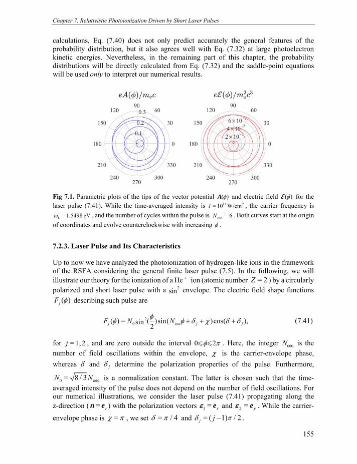
Chapter 7. Relativistic Photoionization Driven by Short Laser Pulses
155
calculations, Eq. (7.40) does not only predict accurately the general features of the probability distribution, but it also agrees well with Eq. (7.32) at large photoelectron kinetic energies. Nevertheless, in the remaining part of this chapter, the probability distributions will be directly calculated from Eq. (7.32) and the saddle-point equations will be used only to interpret our numerical results.
Fig 7.1. Parametric plots of the tips of the vector potential ( )A and electric field ( ) for the laser pulse (7.41). While the time-averaged intensity is 17 2= 10 W/cmI , the carrier frequency is
L = 1.5498 eV , and the number of cycles within the pulse is osc = 6N . Both curves start at the origin
of coordinates and evolve counterclockwise with increasing .
7.2.3. Laser Pulse and Its Characteristics
Up to now we have analyzed the photoionization of hydrogen-like ions in the framework of the RSFA considering the general finite laser pulse (7.5). In the following, we will illustrate our theory for the ionization of a He ion (atomic number = 2Z ) by a circularly polarized and short laser pulse with a 2sin envelope. The electric field shape functions
( )jF describing such pulse are
20 osc( ) = ( )sin( )cos( ),sin
2j j jF N N (7.41)
for = 1, 2j , and are zero outside the interval 0 2 . Here, the integer Nosc is the
number of field oscillations within the envelope, is the carrier-envelope phase,
whereas and j determine the polarization properties of the pulse. Furthermore,
0 = 8 / 3N Nosc is a normalization constant. The latter is chosen such that the time-averaged intensity of the pulse does not depend on the number of field oscillations. For our numerical illustrations, we consider the laser pulse (7.41) propagating along the z-direction ( = zn e ) with the polarization vectors 1 = xe and 2 = ye . While the carrier-
envelope phase is = , we set = / 4 and = ( 1) / 2j j .

Advances in Optics: Reviews. Book Series, Vol. 2
156
The shape functions ( )jf , which define the laser field vector potential ( )A [see,
Eq. (7.5)], can be directly calculated from Eq. (7.41),
0
( ) = d ( ).j jf F
(7.42)
Note that, for >1Nosc , those functions also vanish outside the interval [0,2 ] .
In Fig. 7.1 we present the time evolution of the tips of the vector potential (left panel) and the electric field ( ) = ( )t A (right panel) for the laser pulse defined by (7.41). As the pulse propagates along the z -direction, those plots are generated in the xy-plane. While the number of oscillations is chosen to be = 6Nosc , the averaged intensity is
17 2=10 W/cmI , and the carrier frequency is L osc= =1.5498 eV.N The latter corresponds to a wavelength of 800 nm (Ti-Sapphire). Both curves are presented in relativistic units, where the vector potential is divided by the factor e / | |m c e and the
electric field by 2 3e / | |m c e . Note that the last factor is, up to a minus sign, the so-called
Sauter-Schwinger critical field S [44, 45]. As it can be seen from the right panel of this
figure, the ratio | ( ) | / 1s , thus, the probability of pair production from vacuum is
considered to be negligible [46].
Both curves in Fig. 7.1 evolve counterclockwise with increasing and they start and end
at the origin of coordinates. Furthermore, let us note that the azimuthal angle, = ( ) , can be defined as
1 2= arg( ( ) i ( ) ),e e A A (7.43)
where arg( ) [0, 2 [z is the argument of the complex number z . As it can be seen, is
not uniquely defined by the phase of the laser pulse , as their correspondence is not one-
to-one. Hence, for any specific value of , the vector potential acquires different
magnitudes and the curve ( )A can cross itself at several points.
Another quantity of great interest for our further analysis is the time-dependent ponderomotive energy of an electron in the laser field, defined as
2 2
e
( )( ) = = ( ).
2p p
eU U
m
A (7.44)
Note that, as in the case of the vector potential, the function ( )pU can acquire different
values for the same azimuthal angle . The importance of this observation will be clear
in the following sections.

Chapter 7. Relativistic Photoionization Driven by Short Laser Pulses
157
Up to now, our analytical formulation applies to the photoionization of any hydrogen-like ion with an arbitrary atomic number Z . In such case, its ground state energy is given by [35]
2 2 20 e= 1 .E m c Z (7.45)
However, from now on, we will concentrate our attention on the ionization of light ions, for which 1Z .
7.2.4. Approximate Solution to the Saddle-Point Equation
It is clear that the behavior of the saddle-points determines the regions in the energy spectra of photoelectrons where interference-free and interference-dominated structures are located. Note that, for the laser pulse considered here, the solutions to Eq. (7.38), which defines the saddle points, have to be determined numerically. Instead, one can also construct approximate solutions of (7.38), as we show this below.
Let us start by considering a photoelectron of momentum = p p p n detected at the
azimuthal angle p . We assume that there is a real phase p which satisfies the saddle-
point equation (7.38). The latter can be rewritten in terms of the vector potential [see, Eqs. (7.34) and (7.37)],
2 20 0
0
( ) ( )( ) = = 0.
2
e ep qG
k k p k p
p p
p
A p A (7.46)
Since any real phase p satisfying Eq. (7.46) approximates a dominant saddle point, we
define the former such that [34]
= ( ).e pp A (7.47)
Now, by noting that the scalar products are ( ) = ( )e e p pA p A p and 0 0= ( )k p k p p , it becomes clear that Eq. (7.46) is satisfied provided that
2 2
0 00
( )= = .
2
ep p q
q
pA (7.48)
Therefore, the momentum p constructed in this way is fully determined by the phase
p ,
2 2
0
( )( ) = ( ) .
2
ee
q
p
p p
Ap A n (7.49)

Advances in Optics: Reviews. Book Series, Vol. 2
158
Note, however, that its associated four-momentum is not exactly on the mass-shell. In particular, for a hydrogen-like ion with a ground-state energy given by (7.45), we have that
0 2 2 2 2 2e= ( ) = (1 ).p p q m c Z (7.50)
Nevertheless, if the ion is light enough ( 1Z ) then 2 2ep p m c and we say that p is
nearly on the mass shell.
Let us now analyze the physical consequences derived from the analysis presented above. Eq. (7.47) directly determines the azimuthal angle of photoelectron emission for a phase p ,
1 2= arg[ ( ) ( i )].e p pA (7.51)
Inversely, given the azimuthal angle of detection, a collection of phases p which satisfy
Eq. (7.51) can be determined. Such phases are responsible for large probabilities of ionization in the energy-polar angle spectra of photoelectrons (constant p ), as it will be
discussed in Section 7.5. In contrast, Eq. (7.48) relates the real saddle point p to the
photoelectron energy, 0cp . By rewriting its right-hand side as
2 2
0 00
( )= ,
2
ep q
q
pA
(7.52)
and considering light hydrogen-like ions ( 0eq m c ) we obtain that
2e ( ).pE m c U p p (7.53)
According to the discussion presented in Section 7.2.2, p represents the time when the
photoelectron appears in the continuum. Therefore, one can conclude from Eq. (7.53) that the asymptotic kinetic energy of the photoelectron is approximately equal to its ponderomotive energy in the laser field at its time of birth. Finally, the relation (7.48) also determines the polar angle of photoelectron detection, p , as
0
2 2 2e
cos = = ,| | ( )
E Ep
E m c
p
p
pp
(7.54)
and, therefore, for light ions one obtains
2
e
2e
arccos .E m c
E m c
p
pp
(7.55)

Chapter 7. Relativistic Photoionization Driven by Short Laser Pulses
159
It follows from this formula that the polar angle of electron detection decreases monotonically with its kinetic energy. This is actually expected, as the most energetic photoelectrons absorb a large number of laser photons. As a consequence, the radiation pressure exerted over them is larger than the one experienced by slow photoelectrons.
It is worth mentioning that, for sufficiently large kinetic energies of photoelectrons and for sufficiently light ions, the phase p fully determines several characteristics of the
photoionization considered in this chapter. It does not only determine the regions in space where the probability of ionization is maximal (defined by the angles p and p ) but it
also determines the kinetic energies with which the emitted electrons are most probably detected. Note also that our analysis can be further extended to the strong-field ionization of any light ion or neutral atom. This is due to fact that the high-energy photoelectrons, which are the subject of our study, originate mostly from the atomic K-shell. Moreover, electrons coming from other atomic levels contribute only marginally to the final probability distributions. This can be realized by noting that the vector
0 0= ( ) = = ( )q p e pQ p n p A is the argument of the Fourier transform i ( ) Q
which enters the probability amplitude of ionization (7.24). According to Fig. 7.1, for the laser pulse considered here with the intensity of 17= 10I 2W / cm , the maximum value
achieved by | |p is approximately e 0 00.26 = 0.26 / ( ) = 36 /m c a a , where 0a is the
Bohr radius. This implies that bound electrons located at distances around 00.03a from the atomic nucleus are transferred to the continuum with highest probability. Even more, if the driving field intensity is further increased, this estimated distance is reduced.
7.3. Spiral of Ionization in Momentum Space
According to the derivations presented in the previous section, only photoelectrons characterized by momentum vectors with tips lying in the close vicinity of the three-dimensional spiral (7.49) can be detected with significant probability. Note, however, that Eqs. (7.51), (7.53), and (7.55) define the energy-angular position of the maximum of the interference-free or interference-dominated structures. The width spanned by either of those patterns is finite and depends on p . Therefore, the three-dimensional ionization spiral in momentum space can be represented as a tube closely surrounding the curve given by Eq. (7.49), with a diameter which varies with the parameter p .
In Fig. 7.2 we present the time-dependent ponderomotive energy as a function of the azimuthal angle [Eq. (7.44)] (left panel) together with the momentum spiral of maximum probability of ionization [Eq. (7.49)] (right panel). Both figures are obtained by changing the parameter = p from 0 to (blue curve), which corresponds to the
ramp-up part of the pulse, and from to 2 (cyan curve) for the ramp-down part. The laser field parameters are the same as in Fig. 7.1.

Advances in Optics: Reviews. Book Series, Vol. 2
160
Fig. 7.2. Time-dependent ponderomotive energy as a function of the azimuthal angle ( )pU
[Eq. (7.44)] (left panel) and spiral of ionization in momentum space [Eq. (7.49)] (right panel). Both plots are presented as parametric curves with the parameter = p ranging from 0 to 2 .
The laser field is the same as described in Fig. 7.1. For visual purposes, those portions of the curves which relate to the ramp-up part of the pulse ( 0 < ) are shown in blue, while the ones related
to the ramp-down ( < 2 ) are plotted in cyan.
It can be seen that the function ( )pU is not one-to-one, as it achieves different values for
the same azimuthal angle. Moreover, for the laser pulse considered here, the ponderomotive curve intersects itself at = 0 and . Now, as the asymptotic kinetic energy of the photoelectron is approximately equal to its ponderomotive energy evaluated at p (provided that pU is large enough), the former can be estimated from the left panel
of Fig. 7.2. This is done by drawing a line at constant azimuthal angle and determining the points of its intersection with the ponderomotive curve. From the right panel of the same figure one can see that the three-dimensional spiral also presents several self-intersections. It actually means that, for certain points in the momentum space, there are at least two dominant saddle points p associated with the same asymptotic momentum.
As a consequence, a photoelectron of given final energy can be emitted in the same direction at two different times. Therefore, interference patterns should arise from both such contributions to the probability amplitude [34]. Furthermore, by looking at the definitions of the time-dependent ponderomotive energy [Eq. (7.44)] and the azimuthal angle [Eq. (7.43)], one can see that, for the considered shape of the laser pulse, the self-intersections of the momentum spiral coincide with the self-intersections of the function ( )pU .
Let us now analyze the behavior of the dominant saddle points obtained numerically from Eq. (7.38) along the spiral ( )pp [see, Eq. (7.49)]. In doing so, we choose the phase
= p and calculate the function ( )s for 0 < 2 . In the upper-left panel of Fig. 7.3
we present the imaginary part of the dominant saddle point as a function of the real phase

Chapter 7. Relativistic Photoionization Driven by Short Laser Pulses
161
p . It acquires values close to zero when the ponderomotive energy is sufficiently large;
the latter is shown in the bottom right panel in units of the ionization potential, 2
e 0=pI m c E . Note, however, that Im s increases at the beginning and at the end of the
pulse, when ( )pU is relatively small. In the upper-right panel we compare the
approximate saddle point p with the real part of s . One can see that their difference
goes very fast to zero with increasing the ponderomotive energy. Furthermore, in the lower-left panel we plot the imaginary part of ( )sG evaluated at the dominant saddle point (blue curve). It also acquires small values in the mid-part of the laser pulse and increases in regions of small ponderomotive energy. In the same frame, we present the contribution arising from a second saddle point for which Im ( )sG is also small at certain phases (red curve). It is, therefore, expected that interference-dominated structures will appear in the energy spectra of photoelectrons for p near the contact points of the two
curves. The latter are also identified as the self-intersections of the three-dimensional momentum spiral presented in Fig. 7.2. Finally, by looking at the behavior of the imaginary and real parts of the saddle point (upper panels), we conclude that the approximation s p is valid for the case when ( ) >10p pU Ip , given the laser field
parameters considered here. Now, taking into account that in high-energy ionization Eq. (7.53) holds, we conclude that the validity of our approach coincides with the range of applicability of the RSFA, i.e., it is necessary that 2
e( )p pU E m c I p p .
Moreover, even a better agreement between our estimated saddle point and the exact one is expected, once the intensity of the driving laser field is increased.
7.3.1. Probability of Ionization along the Three-Dimensional Momentum Spiral
As we have learnt in the previous section, photoelectrons are detected with largest probability if the tips of their asymptotic momenta lay on the three-dimensional spiral (see Fig. 7.2). Let us then analyze the spin-independent probability distribution [Eq. (7.32)] along such path. The quantity of interest is the one-dimensional distribution
( ( )) ( ) p , where ( )p is given by Eq. (7.49). In Fig. 7.4 we present this
distribution for two different intensities, 17= 10I W/cm2 (left panel) and 18= 10I W/cm2 (right panel), while maintaining the other laser field parameters the same
as in Fig. 7.1. From the left panel, one can see that ( ) is almost zero at the beginning
and at the end of the laser pulse. The region where 0.5 < < 1.5 is characterized by a relatively constant probability distribution between strong interference structures. The latter are evidenced as dense series of peaks spanning around well defined phases. Such phases coincide with the contact points between the imaginary parts of the function ( )sG evaluated at the two contributing saddle-points, as presented in Fig. 7.3. Furthermore, the regions of small values of ( ) ( < 0.3 and > 1.7 ) coincide with the phase
intervals where Im ( )sG increases. This is not surprising, as the dominant term in the
probability amplitude of ionization (7.39) is proportional to Im ( )
eG s
. With respect to the

Advances in Optics: Reviews. Book Series, Vol. 2
162
interference structures, one can see that the hight of the peaks reach values nearly four times larger than the interference-free ones in their close vicinity. This can be understood by noting that the triply differential probability distribution is proportional to the modulus squared of the amplitude; if two saddle points are characterized by the same imaginary part of ( )sG and both add coherently, constructive interference causes the probability distribution to increase by a factor of four as compared to a single saddle point contribution. This indicates that the photoemission of electrons with momenta defined by the spiral is coherent. Another feature worth mentioning is the small reduction of ( )
around = , i.e., when the electric field acquires its maximum strength. This could be a signature of stabilization against ionization (see, for instance, [47-56]).
Fig. 7.3. Analysis of the dominant saddle point along the spiral ( )pp [Eq. (7.49)] obtained
by the numerical solution of Eq. (7.38). The laser field is the same as described in Fig. 7.1. In the upper-left panel we present Im s as a function of the phase = p . This quantity is very
small provided that the phase is not near to the boundaries, i.e, when the strength of the laser field is large enough. In the upper-right panel we show the difference between = p and the real part
of s . Again, such difference is nearly zero when the phase is not too close to 0 or 2 .
The lower-left panel presents the imaginary part of the function ( )sG [see, Eq. (7.34)] evaluated
at the dominant saddle-point (blue line). As expected, it acquires small values in the mid-part of the pulse. Note, however, that another saddle point relates to small Im ( )sG
only at specific values of (red line). As it follows from our analysis, those regions should be
characterized by strong interference effects. Finally, in the lower-right panel, the time dependent
ponderomotive energy ( )pU [Eq. (7.44)] divided by the ionization potential, 2e 0=pI m c E ,
is presented. While it acquires large values in the mid-part of the laser pulse, it vanishes when the phase approaches 0 or 2 .

Chapter 7. Relativistic Photoionization Driven by Short Laser Pulses
163
Fig. 7.4. One-dimensional spin-independent probability distribution ( ( ))φ p calculated along the spiral of ionization [see, Eqs. (7.32) and (7.49)]. While the laser field intensities are
1710I = W/cm2 (left panel) and 1810I = W/cm2 (right panel), the remaining parameters of the laser pulse are the same as in Fig. 7.1.
When the laser field intensity increases from 17= 10I W/cm2 to 18= 10I W/cm2 we also observe interference-dominated structures in the one-dimensional probability distribution (see the right panel in Fig. 7.4). While the interferences are located at the exact same phases for both intensities, their strength differ considerably. More importantly, a substantial reduction of the ionization probability is observed in the region 0.3 < < 1.7 for 18= 10I W/cm2. This, as well, reflects in lowering the hight of the interference peaks in this interval. Note that the phase regions of negligible probability, located at the beginning and at the end of the pulse, are shorter for larger driving field intensities. One can analyze these results using the saddle-point approach. In Fig. 7.5 we show the same as in Fig. 7.3 but for 18= 10I W/cm2.
Fig. 7.5. The same as in Fig. 7.3 but for a driving laser field intensity 18 2= 10 W/cmI .

Advances in Optics: Reviews. Book Series, Vol. 2
164
By comparing the upper panels of those two figures one can see the expected improvement of the approximation s p ; while the imaginary part of s achieves smaller values
along a larger range of phases, the difference Re s goes rapidly to zero. Such an improvement is also consistent with a faster increase of the ponderomotive energy during the ramp-up part of the pulse (see the scale in the lower-right panels of both figures). By comparing the lower-left panels, it can be seen that the contact points of Im ( )sG , evaluated at the two contributing saddle points, are located at the same phases, independently of the intensity. Nevertheless, for 18= 10I 2W/cm , the blue curve decreases faster and achieves smaller values in the mid-part of the pulse. Such fast decrease explains the larger probabilities around the strong interference structures evidenced at 0.3 and 1.7 in the right panel of Fig. 7.4. This happens in
regions before and after the valley in the probability distribution is observed.
7.4. Energy Spectra of Photoelectrons
Now we will consider the energy spectra of photoelectrons at fixed direction in space, determined by the angles ( , ) p p . In Fig. 7.6 we present the spin-independent probability
distributions ( ) p calculated from Eq. (7.32) for the same laser field parameters as in
Fig. 7.1. While the azimuthal angles have been chosen to be = p (left panel) and
= 0 p (right panel), the polar angles are such that the energy distribution reaches its
maximum along that specific direction. From the left panel, where ( , ) = ( ,0.4655 ), p p one can see an interference-dominated structure characterized by
a dense series of peaks within a gaussian-type envelope. This envelope has a full-width-at-half-maximum (FWHM) of roughly 1.4 keV and its maximum is located at 13.7 keV. On the other hand, for ( , ) = (0,0.4605 ) p p (right panel) two well-defined structures
appear in the energy spectrum of photoelectrons. While the lower-energy one is located at 9.5 keV and presents strong interferences, the higher-energy structure is maximal at 16.8 keV and can be recognized as a supercontinuum. Note that, according to our previous analysis, it should be possible to predict certain properties of those structures by analyzing the time-dependent ponderomotive curve. To illustrate this, we note that a line drawn at
= = p in the left panel of Fig. 7.2 would intersect the ( )pU -spiral at two points,
each of them being a self-intersection. Therefore, at this particular azimuthal angle, only interference-dominated structures are expected to be encountered. Furthermore, in the high-energy part of the spectrum, the maximum probability should be located at around
2 2e e0.027 =13.8E m c m c p keV (intersection of the outer rings of the ponderomotive
curve with the line = ), which very well estimates the position of the actual maximum
in the energy distribution. Now, the line = 0 would intersect the curve ( )pU at three
different points. The outermost one predicts the formation of a supercontinuum located at 2 2
e e= 0.033 16.9E m c m c p keV, which is very close to the actual position of the

Chapter 7. Relativistic Photoionization Driven by Short Laser Pulses
165
maximum of the smooth lobe shown in the right panel of Fig. 7.6. Moreover, the second crossing happens at the self-intersection of the ponderomotive curve. Thus, in agreement with our numerical results, an interference-dominated pattern is expected at
2e 9.4E m c p keV.
Fig. 7.6. Spin-independent energy spectra of photoelectrons ( ) p [Eq. (7.32)] calculated at constant polar and azimuthal angles, as specified in each frame. The laser field parameters are
the same as in Fig. 7.1.
In Fig. 7.7 we present the energy spectra of photoelectrons ( ) p [Eq. (7.32)], calculated
for the laser field intensity 18 2=10 W/cmI along the directions ( , ) = ( ,0.388 ) p p
(left panel) and (0,0.38 ) (right panel)1. Here, we only concentrate on the most energetic portion of the distributions. By comparing Figs. 7.6 and 7.7, it is clear that the maxima of the probability distributions are found at ten times larger photoelectron kinetic energies when the field intensity increases by one order of magnitude. This is in agreement with Eq. (7.53), which indicates that the electron kinetic energy depends linearly on the driving laser field intensity. Moreover, the polar angles of detection decrease from around 0.46 to 0.38 . This, in turn, agrees with Eq. (7.55), which predicts that the larger the kinetic energy the smaller polar angles of photoelectrons. From the left panel of Fig. 7.7, we can estimate that the FWHM of the envelope of the interference-dominated structure is around 7 keV, which is approximately five times larger than the width of the structure presented in the left panel of Fig. 7.6. Moreover, by comparing the right panels of both figures, one can see that the width of the supercontinuum increases about three times (from 2 keV up to 6 keV) for the larger intensity. As it will be shown in the next section, this observation implies that the central energy and bandwidth of each structure augment with the driving field intensity at different rates.
In summary, we have shown that in high-energy ionization, the probability distributions at fixed directions in space can present interference-dominated or interference-free
1As it was done in Fig. 7.6, the polar angles of detection are chosen such that the probability distribution acquires its maximum values along this specific direction.

Advances in Optics: Reviews. Book Series, Vol. 2
166
(supercontinua) structures, just as predicted in Section 7.3. Furthermore, we have proven that such patterns present a maximum probability at energies given by (7.53) and that their widths increase with the intensity of the driving field. Now we will further analyze the polar-angle dependence of the energy spectra of photoelectrons.
Fig. 7.7. The same as in Fig. 7.6 but for the laser field intensity 18 2= 10 W/cmI . This time,
the polar and azimuthal angles correspond to ( , ) = ( ,0.388 ) p p
(left panel)
and ( , ) = (0,0.38 ) p p
(right panel).
7.5. Energy-Angular Probability Distributions
In Fig. 7.8 we present the color mappings of the energy-polar angle probability distributions calculated from Eq. (7.32) for the same laser field parameters as in Fig. 7.1. Each plot relates to a different azimuthal angle = p , as specified in the upper part of
the panels. In all nine cases, cigar-type structures present maximum probabilities at polar angles and kinetic energies as predicted by Eqs. (7.53) and (7.55), provided that the photoelectrons are sufficiently energetic. Furthermore, while some of the structures are interference-free, others exhibit strong interferences. The latter show very fine fringes of large and small probabilities, which compose the overall structure. However, as those patterns are not visible in the present scale, we shall indicate the regions where the interferences occur. Starting from = 0 p (upper-left panel), one can observe three well-
defined islands at the low-, mid-, and high-energy parts of the distributions. While the latter is associated to a supercontinuum, the other two present strong interferences. Now, by slowly increasing the azimuthal angle of detection, the interference-dominated patterns gradually transform into four supercontinua, while still presenting the characteristic fringes at the points of contact. They become almost fully separated at = 0.375 p
(mid-left panel), before the two interference-free islands of highest energy start to merge. Finally, at = p , all structures observed within the chosen range of polar angles and
kinetic energies, coalesce into two well-defined interference-dominated patterns (lower-right panel).

Chapter 7. Relativistic Photoionization Driven by Short Laser Pulses
167
Fig. 7.8. Color mappings of the spin-independent probability distribution ( ) p [Eq. (7.32)]
as a function of the polar angle θ p and the photoelectron kinetic energy 2eE m cp . Each plot is
generated at different azimuthal angle φ = φp ranging from 0 to π , as indicated in the upper part
of the frames. The laser field parameters are the same as in Fig. 7.1.
Note that most of the above observations can be predicted from the left panel of Fig. 7.2. First, we see that the line = 0 crosses the ponderomotive curve exactly three times, at low-, mid- and high-energies. The first two crossings coincide with self-intersections of the ( )pU -spiral and, hence, they correspond to the interference-dominated structures
shown in the upper-left panel of Fig. 7.8. A different character has the high-energy intersection, resulting in a broad supercontinuum observed in the energy-angular distribution of photoelectrons (see, also the analysis of Fig. 7.6 for the constant polar angle
= 0.4605 p ). Now, by increasing = p , the arcs of the ( )pU -spiral gradually
separate, with the consequent formation of four interference-free patterns. For even larger azimuthal angles, the arcs of the ponderomotive curve start to approach each other such that, at = , the curve intersects itself twice. This explains the formation of the well-defined interference-dominated patterns in the lower-right panel of Fig. 7.8.
It is important to keep in mind that the ponderomotive curve in Fig. 7.2 only accounts for the regions of maximum probability of ionization and does not relate to the spread of the structures presented in Fig. 7.8. A detailed analysis of the ’diameter’ of the tube which surrounds the spiral would also predict the actual shape and extent of the high-probability islands in the energy-angular distributions. Still, several conclusions can be drawn from Fig. 7.8. It can be seen, for instance, that, while the energy spread ( E p ) of each

Advances in Optics: Reviews. Book Series, Vol. 2
168
independent distribution increases with the photoelectron kinetic energy, the angular spread ( p ) decreases. This is of great importance for the synthesis of singe-electron
wave packets of short duration, as it will be explained in the next section. Furthermore, by properly choosing the polar and azimuthal angles of detection, it should be possible to observe not only interference-dominated and interference-free patterns, but also structures presenting both characteristics at different kinetic energies in the spectrum of photoelectrons.
In Fig. 7.9 we present the energy-polar angle distribution calculated from Eq. (7.32) for the same azimuthal angles as in Fig. 7.8. This time, we set the laser field intensity to be
18= 10I 2W/cm . It can be seen, by comparing those two figures, that the high-probability islands behave in the same way while changing = p . This is actually expected, as the
ponderomotive curve conserves its original shape while presenting larger values. Furthermore, the position of the maximum probabilities are, again, as predicted by Eqs. (7.53) and (7.55). Note that in Fig. 7.9 such maxima are located at exactly ten times larger kinetic energies as compared to the ones in Fig. 7.8, which is consistent with our previous analysis. Moreover, for stronger laser fields, each independent structure presents a considerably larger spread in energy and a smaller spread in polar angles. Nevertheless, all of them are more localized in energy, in the sense that the ratio /E E p p
center , where
Epcenter is the position of maximum probability, is smaller. This also supports the idea that
E p does not scale with intensity in the same way as the central energy does.
Fig. 7.9. The same as in Fig. 7.8 but for a driving field intensity of 18 2= 10 W/cmI .

Chapter 7. Relativistic Photoionization Driven by Short Laser Pulses
169
Up to now we have analyzed the energy spectra of photoelectrons for different polar and azimuthal angles in the context of ionization of light ions. We have shown that interference-free and interference-dominated patterns can be encountered at different portions of the spectra, depending on the direction of detection. In the next section we will demonstrate that the supercontinua can be used to generate very short single-electron wave packets, which is of great interest in light of its application in the four-dimensional electron microscopy.
7.6. Application: Generation of Single-Electron Wave Packets
It has been recently demonstrated that single-electron wave packets can be generated from supercontinua arising in the ionization of light ions driven by circularly polarized laser fields [31-34]. Moreover, it was proven that, in the domain of supercontinuum formation, the probability amplitude of ionization is characterized by a phase with approximately constant first derivative with respect to the electron energy. This leads to the creation of chirpless electron pulses with a constant time delay, which only depends on their propagation direction. Furthermore, according to the uncertainty principle, it is expected that interference-free patterns with a small energy spread would produce long-in-time electron wave packets. Thus, in order to obtain pulses with attosecond duration, supercontinua of large bandwidth need to be considered. As we will demonstrate shortly, this can be done by synthesizing the electron pulses from the high-energy part of the spectrum for large intensities of the laser field.
Electron wave packets, i
( )x , are constructed as a superposition of probability
amplitudes of different momenta along a specific direction of space, 0n , and with kinetic
energies in a given range. Namely,
23
ie3i i
d( ) = e ( ) ( ),
(2 )p xm cV p
x uVE
pp
p p (7.56)
where
2 2 (2)max e e min 0
( ) = ( ) ( ) ( )E E m c E m c E p p p np (7.57)
is a filter function and i
( ) p is the spin-dependent probability amplitude of ionization
[Eq. (7.26)]. The former selects the kinetic energies, 2min e maxE E m c E p , together with
the spatial direction of detection, given by the solid angle 0
n . Now, by inserting
Eq. (7.57) into (7.56), we obtain that the space-time probability amplitude can be calculated as the one-dimensional integral
2 i( | | )max e
| | , 02i 0 imin e
( , ) = d e | | (| | ),E m c E t d
E m ct d N E u E
ppp p n p p p n (7.58)

Advances in Optics: Reviews. Book Series, Vol. 2
170
where N is an irrelevant constant term. Note that the above space-time amplitude
implicitly contains the factor 2i ee
m c t, which introduces fast oscillations of the integrand
but does not play a role in the calculation of probabilities. Thus, for our further analysis, we define
2i e
i i( , ) = e ( , ).
m c tt d t d
(7.59)
Furthermore, the space-time spin-dependent probability distribution, calculated at a distance 0=d x n from the parent ion1, is given by
†
i i i( , ) = [ ( , )] ( , ),t d t d t d (7.60)
where both the initial and final spins are projected onto the laser field propagation direction, i.e., ze .
In Fig. 7.10 we present the space-time probability distributions ( , )t d [Eq. (7.60)], normalized to 1, for the same laser field parameters as in Fig. 7.1. The directions of detection are given by the angles 0 0( , ) = ( ,0.4655 ) (upper row) and (0,0.4605 ) (lower row), which correspond to the distributions shown in the left and right panels of Fig. 7.6, respectively. While in the left column we present the results for the distance d at which the electron just escaped the laser field ( = 2k x ), in the right column we
consider the mesoscopic distance 50= 2 10 10 md a . Note that we present only the
space-time distributions for i( , ) = ( , ) as the scaled results for other initial and final spin states are the same. For the numerical calculations, we have chosen the kinetic energy boundaries min max( , )E E = (11 keV, 16.5 keV) for the upper row, and
min max( , )E E = (0, 20 keV) for the lower one [see, Eq. (7.58)].
By looking at the left panel in Fig. 7.6 and the upper-left panel in Fig. 7.10, we can see that the interference-dominated pattern observed in the former, leads to a double-hump space-time distribution, characterized by two well-defined lobes detected at different times. The duration of each wave packet (calculated from the FWHM of the lobes) is approximately 600 as. Note, however, that at mesoscopic distances (upper-right panel of Fig. 7.10) those two structures interfere, with the consequent formation of dense series of peaks in the space-time distribution. Furthermore, the FWHM of the envelope is associated to a time duration of nearly 8 fs. Now, by analyzing the right panel in Fig. 7.6 together with the lower panels in Fig. 7.10 it is clear that, at short distances ( 4
0= 2.9 10 1.5 md a ) the interference-dominated pattern also leads to a double-hump structure. However, the independent lobes merge together with the formation of an
1We assume that the dynamics of the parent ion in the laser field is much slower than the electron motion, due to its larger mass. Therefore, we consider the former to be fixed in space during ionization.

Chapter 7. Relativistic Photoionization Driven by Short Laser Pulses
171
interference-rich pattern at larger distances from the parent ion. In contrast, the supercontinuum observed in the high-energy portion of the spectrum (central kinetic energy around 17 keV) produces a well-defined electron wave packet lasting for 1.3 fs at
= 1.5 md . Note that, after propagating in space, the duration of the electron pulse
increases, reaching around 7 fs at 10 md . This is actually expected, as photoelectrons
with sub-relativistic kinetic energies (much smaller than 2em c ) present the dispersion
relation 2 2 2e= ( ) ( )E m c cp p . As a consequence, the group and phase velocities differ,
and the wave packet spreads rapidly in time.
Fig. 7.10. Normalized space-time probability distributions ( )t,d [Eq. (7.60)] calculated for the
propagation directions 0 0( , ) = ( ,0.4655 ) (upper row) and (0,0.4605 ) (lower row). Note that
those distributions are obtained from the energy spectra of photoelectrons presented in the left and right panels of Fig. 7.6, respectively. The laser field parameters are the same as in Fig. 7.1 and the electron-nucleus separation 0=d x n is specified in each panel. While the left column relates to
distances at which the electron just left the laser pulse ( = 2k x ), the right column presents
the probability profiles at the mesoscopic distance of 502 10 ,a where 0a is the Bohr radius. In
obtaining those plots, we have set the maximum and minimum kinetic energy [see, Eq. (7.58)] to
min max(E ,E ) =(11 keV, 16.5 keV) for the upper panels, and min max(E ,E ) =(0, 20 keV) for the lower
panels.
It is now interesting to perform the space-time analysis for the ionization driven by more intense laser fields. We know that, in this case, the high-probability islands in the energy-polar angle plane present larger bandwidths and appear with larger kinetic energies. Hence, it is expected that the synthesized electron pulses would last for shorter periods of time and spread less during propagation. In Fig. 7.11 we present the space-time probability distributions ( , )t d , but this time for a laser field intensity of 18 2=10 W/cmI . The

Advances in Optics: Reviews. Book Series, Vol. 2
172
directions of detection are 0 0( , ) = (0,0.38 ) (upper row) and ( ,0.388 ) (lower row), which correspond to the spectra of photoelectrons shown in the right and left panels of Fig. 7.7, respectively. One can see that the supercontinuum from the right panel of Fig. 7.7 relates to a well-defined electron wave packet which lasts for around 250 as and propagates with a central kinetic energy of nearly 167 keV ( 2
e0.33m c ). After traveling
a distance 10 md the pulse lasts for only 630 as. Now, considering the interference structure in the left panel of Fig. 7.7 we observe again the formation of two well-defined lobes in the space-time probability distribution. Each one of them presents a FWHM of 450 as at the distance 4
0= 9.2 10 5 m.d a However, at 10 m,d both humps approach each other while their duration increase up to approximately 1 fs. Note that, at their contact points, interference patterns start to build up.
Fig. 7.11. The same as in Fig. 7.10 but for the laser field of intensity 18 2= 10 W/cmI and the
directions of detection 0 0( , ) = (0,0.38 ) (upper row) and ( ,0.388 ) (lower row). The space-time
probability distributions correspond to the spectra shown in Fig. 7.7 and have been calculated with
min max(E ,E ) =(125 keV, 150 keV) for the lower row and min max(E ,E ) = (155 keV, 180 keV) for the
upper one [see, Eq. (7.58)].
Other advantage of constructing electron wave packets from the high-energy supercontinua is the relatively small polar-angle window of emission. As it was discussed in the previous section, the angular spread p diminishes with increasing the central
energy of photoelectrons. Even more, it can be further reduced with an increment of the laser field intensity. Hence, it is possible to create a highly-directional source of energetic

Chapter 7. Relativistic Photoionization Driven by Short Laser Pulses
173
and very short single-electron wave packets from ionization driven by circularly (or, in general, elliptically) polarized laser pulses.
7.7. Conclusions
In this chapter, we have analyzed the photoionization process driven by intense, short, and circularly polarized laser fields under the scope of the RSFA. As we have shown, the energy spectra of photoelectrons can present two different types of structures: interference-dominated and interference-free (also recognized as the supercontinuum). While the former is characterized by dense series of peaks, the latter presents a smooth probability distribution which does not vary rapidly in the range of several hundreds of electronvolts. In Section 7.2.2, the saddle-point method was presented as a powerful tool in the analysis of the probability amplitudes. Such approximation predicts the main characteristics of the energy spectra of photoelectrons and it agrees well with the exact distributions calculated for high-energy ionization in the framework of the RSFA. Furthermore, we have constructed an approximate solution to the saddle-point equation which amazingly well describes the actual behavior of the dominant saddle point, provided that the photoelectrons are detected with sufficiently high kinetic energies. This allowed us to define the three-dimensional momentum spiral, which contains most of the information regarding the photoionization of light ions. Such structure does not only locate the regions in energy and space where the probability of electron detection is maximal, but it also determines which regions present interference patterns and which do not. Moreover, a more detailed analysis of the diameter and internal structure of the spiral at different points in the momentum space, would permit us to estimate the polar angle and energy spreads of the islands in the probability distributions. Thus, this three-dimensional curve has the power to fully characterize the photoionization process. For this reason, we consider the spiral in momentum space as one of the most important graphical and analytical tools in the understanding of high-energy photoionization of light ions driven by, in general, elliptically polarized laser pulses.
The second part of this chapter was devoted to the analysis of the spectra of photoelectrons at constant azimuthal angles for two laser field intensities. While it was demonstrated that the actual distributions show maximum values at the energies and polar angles predicted by Eqs. (7.53) and (7.55), i.e., we confirmed the predictions arising from the momentum spiral, also the width of the individual structures was taken into account. As it follows from the results presented in Sections 7.4 and 7.5, the energy spread of the supercontinua increases towards the most energetic parts of the spectrum. In contrast, their polar angle width decreases with Ep . Moreover, by employing laser pulses of larger intensity, the
energy and angular spreads are further augmented and contracted, respectively.
With respect to the synthesis of ultrashort single-electron wave packets, we have shown that the best conditions are met when the interference-free structures of highest energy are used. Their large bandwidth, regular behavior of the amplitude phases, and smooth variations of probability, lead to the generation of electron pulses as short as 630 attoseconds at the mesoscopic distance of 10 m. Additionally, their small angular

Advances in Optics: Reviews. Book Series, Vol. 2
174
spread guarantees that the pulses are most probably detected at a well-defined polar angle. Note, however, that the interference-dominated structures lead to a double-hump space-time probability distribution. While it can be used for pump and probe experiments with the same electron, it has to be done for samples located very near to the photoelectron source. This is due to fact that the humps tend to interfere strongly at relatively short distances from the parent ion, depending on their kinetic energy.
Acknowledgements
This work is supported by the National Science Centre (Poland) under Grant No. 2014/15/B/ST2/02203.
References
[1]. G. Mainfray, C. Manus, Multiphoton ionization of atoms, Rep. Prog. Phys., Vol. 54, 1991, pp. 1333-1372.
[2]. P. A. Franken, A. E. Hill, C. W. Peters, G. Weinreich, Generation of optical harmonics, Phys. Rev. Lett., Vol. 7, 1961, pp. 118-119.
[3]. J. A. Giordmaine, Mixing of light beams in crystals, Phys. Rev. Lett., Vol. 8, 1962, pp. 19-20.
[4]. P. A. Franken, J. F. Ward, Optical harmonics and nonlinear phenomena, Rev. Mod. Phys., Vol. 35, 1963, pp. 23-39.
[5]. G. S. Voronov, N. B. Delone, Ionization of the Xe atom by electric field of a ruby laser emission, JETP Letters, Vol. 1, 1965, pp. 66-68.
[6]. G. S. Voronov, N. B. Delone, Many-photon ionization of the xenon atom by ruby laser radiation, Sov. Phys. JETP, Vol. 23, 1966, pp. 54-58.
[7]. G. S. Voronov, G. A. Delone, N. B. Delone, O. V. Kudrevatova, Multi-photon ionization of the hydrogen molecule in the strong electric field of ruby laser emission, JETP Letters, Vol. 2, 1965, pp. 237-238.
[8]. L. V. Keldysh, Ionization in the field of a strong electromagnetic wave, Sov. Phys. JETP, Vol. 20, 1965, p. 1307.
[9]. F. H. M. Faisal, Multiple absorption of laser photons by atoms, J. Phys. B, Vol. 6, 1973, pp. L89-L92.
[10]. H. R. Reiss, Effect of an intense electromagnetic field on a weakly bound system, Phys. Rev. A, Vol. 22, 1980, pp. 1786-1813.
[11]. H. R. Reiss, Relativistic strong-field photoionization, J. Opt. Soc. Am. B, Vol. 7, 1990, pp. 574-586.
[12]. ELI Beamlines, www.eli-beams.eu [13]. Exawatt Center for Extreme Light Studies (XCELS), http://www.xcels.iapras.ru [14]. R. Srinivasan, V. A. Lobastov, C.-Y. Ruan, A. H. Zewail, Ultrafast Electron Diffraction
(UED): A new development for the 4D Determination of transient molecular structures, Helv. Chim. Acta, Vol. 86, 2003, pp. 1763-1838.
[15]. A. H. Zewail, Diffraction, crystallography and microscopy beyond three dimensions: structural dynamics in space and time, Philos. Trans. R. Soc. London A, Vol. 363, 2005, pp. 315-329.
[16]. V. A. Lobastov, R. Srinivasan, A. H. Zewail, Four-dimensional ultrafast electron microscopy, Proceedings of the Natl. Acad. Sci. U.S.A., Vol. 102, 2005, pp. 7069-7073.

Chapter 7. Relativistic Photoionization Driven by Short Laser Pulses
175
[17]. W. E. King, G. H. Campbell, A. Frank, B. Reed, J. F. Schmerge, B. J. Siwick, B. C. Stuart, P. M. Weber, Ultrafast electron microscopy in materials science, biology, and chemistry, J. Appl. Phys., Vol. 97, 2005, 111101.
[18]. A. H. Zewail, Four-dimensional electron microscopy, Science, Vol. 328, 2010, pp. 187-193. [19]. H. Ihee, V. A. Lobastov, U. M. Gomez, B. M. Goodson, R. Srinivasan, C. Y. Ruan,
A. H. Zewail, Direct imaging of transient molecular structures with ultrafast diffraction, Science, Vol. 291, 2001, pp. 458-462.
[20]. V. A. Lobastov, R. Srinivasan, B. M. Goodson, C.-Y. Ruan, J. S. Feenstra, A. H. Zewail, Ultrafast Diffraction of Transient Molecular Structures in Radiationless Transitions, J. Phys. Chem. A, Vol. 105, 2001, pp. 11159-11164.
[21]. D. A. Plemmons, P. K. Suri, D. J. Flannigan, Probing structural and electronic dynamics with ultrafast electron microscopy, Chem. Mater., Vol. 27, 2015, pp. 3178-3192.
[22]. B. J. Siwick, J. R. Dwyer, R. E. Jordan, R. J. D. Miller, An atomic-level view of melting using femtosecond electron diffraction, Science, Vol. 302, 2003, pp. 1382-1385.
[23]. N. Gedik, D.-S. Yang, G. Logvenov, I. Bozovic, A. H. Zewail, Nonequilibrium phase transitions in cuprates observed by ultrafast electron crystallography, Science, Vol. 316, 2007, pp. 425-429.
[24]. P. Baum, D.-S. Yang, A. H. Zewail, 4D visualization of transitional structures in phase transformations by electron diffraction, Science, Vol. 318, 2007, pp. 788-792.
[25]. P. Baum, A. H. Zewail, 4D attosecond imaging with free electrons: Diffraction methods and potential applications, Chem. Phys., Vol. 366, 2009, pp. 2-8.
[26]. G. Sciaini, R. J. D. Miller, Femtosecond electron diffraction: heralding the era of atomically resolved dynamics, Rep. Prog. Phys., Vol. 74, 2011, 096101.
[27]. M. Aidelsburger, F. O. Kirchner, F. Krausz, P. Baum, Single-electron pulses for ultrafast diffraction, Proceedings of the Natl. Acad. Sci. U.S.A., Vol. 107, 2010, pp. 19714-19719.
[28]. A. Paarmann, M. Gulde, M. Müller, S. Schäfer, S. Schweda, M. Maiti, C. Xu, T. Hohage, F. Schenk, C. Ropers, R. Ernstorfer, Coherent femtosecond low-energy single-electron pulses for time-resolved diffraction and imaging: A numerical study, J. Appl. Phys., Vol. 112, 2012, 113109.
[29]. F. O. Kirchner, S. Lahme, F. Krausz, P. Baum, Coherence of femtosecond single electrons exceeds biomolecular dimensions, New J. Phys., Vol. 15, 2013, 063021.
[30]. P. Baum, On the physics of ultrashort single-electron pulses for time-resolved microscopy and diffraction, Chem. Phys., Vol. 423, 2013, pp. 55-61.
[31]. K. Krajewska, J. Z. Kamiński, Supercontinuum in ionization by relativistically intense and short laser pulses: Ionization without interference and its time analysis, Phys. Rev. A, Vol. 94, 2016, 013402.
[32]. F. Cajiao Vélez, J. Z. Kamiński, K. Krajewska, Ionization without interference, J. Phys.: Conf. Ser., Vol. 826, 2017, 012010.
[33]. K. Krajewska, F. Cajiao Vélez, J. Z. Kamiński, Generation of attosecond electron pulses using petawatt lasers, Proceedings of SPIE, Vol. 10241, 2017, 102411J.
[34]. J. Z. Kamiński, F. Cajiao Vélez, K. Krajewska, High-energy ionization by relativistically intense laser pulses, Laser Phys. Lett., Vol. 14, 2017, 075301.
[35]. J. D. Bjorken, S. D. Drell, Relativistic Quantum Mechanics, McGraw-Hill, New York, 1964. [36]. D. M. Wolkow, Über eine Klasse von Lösungen der Diracschen Gleichung, Z. Phys., Vol. 94,
1935, pp. 250-260 (in Germany). [37]. F. Ehlotzky, K. Krajewska, J. Z. Kamiński, Fundamental processes of quantum
electrodynamics in laser fields of relativistic power, Rep. Prog. Phys., Vol. 72, 2009, 046401. [38]. A. Di Piazza, C. Müller, K. Z. Hatsagortsyan, C. H. Keitel, Extremely high-intensity laser
interactions with fundamental quantum systems, Rev. Mod. Phys., Vol. 84, 2012, pp. 1177-1228.

Advances in Optics: Reviews. Book Series, Vol. 2
176
[39]. K. Krajewska, J. Z. Kamiński, Compton process in intense short laser pulses, Phys. Rev. A, Vol. 85, 2012, 062102.
[40]. K. Krajewska, J. Z. Kamiński, Breit-Wheeler process in intense short laser pulses, Phys. Rev. A, Vol. 86, 2012, 052104.
[41]. K. Krajewska, C. Müller, J. Z. Kamiński, Bethe-Heitler pair production in ultrastrong short laser pulses, Phys. Rev. A, Vol. 87, 2013, 062107.
[42]. E. Yakaboylu, M. Klaiber, K. Z. Hatsagortsyan, Above-threshold ionization with highly charged ions in super-strong laser fields: III. Spin effects and its dependence on laser polarization, Phys. Rev. A, Vol. 91, 2015, 063407.
[43]. K. Krajewska, J. Z. Kamiński, Radiation pressure in strong-field-approximation theory: Retardation and recoil corrections, Phys. Rev. A, Vol. 92, 2015, 043419.
[44]. F. Sauter, Über das Verhalten eines Elektrons im homogenen elektrischen Feld nach der relativistischen Theorie Diracs, Z. Phys., Vol. 69, 1931, pp. 742-764 (in Germany).
[45]. J. Schwinger, On Gauge invariance and vacuum polarization, Phys. Rev., Vol. 82, 1951, pp. 664-679.
[46]. Y. I. Salamin, S. X. Hu, K. Z. Hatsagortsyan, C. H. Keitel, Relativistic high-power laser–matter interactions, Phys. Rep., Vol. 427, 2006, pp. 41-155.
[47]. M. Gavrila, J. Z. Kamiński, Free-free transitions in intense high-frequency laser fields, Phys. Rev. Lett., Vol. 52, 1984, pp. 613-616.
[48]. M. J. Offerhaus, J. Z. Kamiński, M. Gavrila, Coulomb scattering in intense, high-frequency laser fields, Phys. Lett. A, Vol. 112, 1985, pp. 151-155.
[49]. M. V. Fedorov, A. M. Movsesian, Field-induced effects of narrowing of photoelectron spectra and stabilisation of Rydberg atoms, J. Phys. B, Vol. 21, 1988, p. L155.
[50]. M. Pont, M. Gavrila, Stabilization of atomic hydrogen in superintense, high-frequency laser fields of circular polarization, Phys. Rev. Lett., Vol. 65, 1990, pp. 2362-2365.
[51]. D. P. Crawford, H. R. Reiss, Stabilization in relativistic photoionization with circularly polarized light, Phys. Rev. A, Vol. 50, 1994, pp. 1844-1850.
[52]. M. P. de Boer, J. H. Hoogenraad, R. B. Vrijen, R. C. Constantinescu, L. D. Noordam, H. G. Muller, Adiabatic stabilization against photoionization: An experimental study, Phys. Rev. A, Vol. 50, 1994, pp. 4085-4098.
[53]. A. M. Popov, O. V. Tikhonova, E. A. Volkova, Strong-field atomic stabilization: numerical simulation and analytical modelling, J. Phys. B, Vol. 36, 2003, pp. R125-R165.
[54]. A. V. Bogatskaya, A. M. Popov, Stabilization of atoms in strong non-classical electromagnetic fields, J. Phys.: Conf. Ser., Vol. 461, 2013, 012047.
[55]. M. Yu. Emelin, M. Yu. Ryabikin, Atomic photoionization and dynamical stabilization with subrelativistically intense high-frequency light: Magnetic-field effects revisited, Phys. Rev. A, Vol. 89, 2014, 013418.
[56]. A. V. Bogatskaya, E. A. Volkova, A. M. Popov, Spontaneous transitions in atomic system in the presence of high-intensity laser field, Europhys. Lett., Vol. 116, 2016, 14003.

Chapter 8. Direct Femtosecond Laser Writing of Nonlinear Photonic Crystals
177
Chapter 8 Direct Femtosecond Laser Writing of Nonlinear Photonic Crystals
Yan Sheng, Xin Chen and Wieslaw Krolikowski1
8.1. Quasi-Phase Matching and Nonlinear Photonic Crystals
Nonlinear optical processes, which govern the interaction of strong optical signals (e.g., laser beams or pulses) with the media in which these signals propagate, are of great importance for creation of coherent light sources at the frequency bands where the conventional lasers either perform poorly or are unavailable at all [1]. Moreover, the nonlinear processes are of interest because of their potential application in signal processing, mode-locking, pulse compression, etc. [2-4]. The efficiency of a nonlinear parametric process critically depends on relative phase locking of the interacting waves, which is formally expressed by the so-called phase matching condition requiring that phase velocities of all involved waves coincide. In typical optical media this condition cannot be naturally satisfied due to the refractive index dispersion.
A traditional technique for achieving phase matching in nonlinear crystals is birefringent phase matching, where one exploits angular or/and temperature dependence of birefringence to cancel the phase mismatch [5]. However, this approach is ineffective for weakly birefringent materials and eventually a much more versatile technique, the so-called quasi-phase matching (QPM) which relies on a spatial modulation of the quadratic (χ(2)) nonlinearity, was proposed in the 1960s [6, 7]. This spatial nonlinearity variation offers a set of reciprocal lattice wave vectors to compensate the phase mismatch between the interacting waves. Taking the simplest case of the second harmonic generation in a one-dimensional periodic χ(2) structure as an example, the QPM condition is written as k2-2k1-Gm = 0, where k1, k2 represent wave vectors of the fundamental and second harmonic beams, respectively, Gm = 2mπ/Λ is the reciprocal lattice vector with Λ denoting the period of χ(2) structure and m being an integer (Fig. 8.1(a)). While initially the QPM structures had been restricted to one-dimensional χ(2) modulation (also called optical
Yan Sheng Laser Physics Center, Research School of Physics and Engineering, Australian National University Canberra, Australia

Advances in Optics: Reviews. Book Series, Vol. 2
178
superlattice), the concept was generalized to two-dimensional structures by V. Berger in 1998 [8]. From then on, the artificial microstructures with a constant linear susceptibility χ(1), but a spatially modulated nonlinear susceptibility tensor χ(2) have been called nonlinear photonic crystals (NPC), as a nonlinear optical analogue of the well-known linear photonic crystals [9]. Comparing with the 1D superlattices, the 2D NPC have more plentiful reciprocal lattice vectors in multiple directions, thereby enabling simultaneous phase matching of different nonlinear optical processes in a single crystal (see Figs. 8.1(b) and 8.1(c) for an example) [10]. So far, a variety of NPC structures, including periodic [11], quasi-periodic [12-14], short-range ordered [15,16], radial symmetric [17] and even inherently random nonlinear photonic structures [18, 19], have been developed to facilitate practical applications such as high order harmonic generators [20], optical frequency combs [21], and entangled photon sources, etc. [22, 23].
Fig. 8.1. (a) Illustrating the concept of quasi-phase matching (QPM) in one-dimensional optical superlattice, where the quadratic (χ(2)) nonlinear coefficient is periodically modulated to compensate phase mismatch of a nonlinear optical process by reciprocal lattice vectors (Gm = 2mπ/Λ). (b) An example of two-dimensional nonlinear photonic crystal (NPC), which offers plentiful reciprocal lattice vectors that allow quasi-phase matching of multiple nonlinear optical processes in different directions (c).
8.2. Traditional Fabrication Methods of Nonlinear Photonic Crystals
Ferroelectric crystals are the most commonly used materials for the fabrication of nonlinear photonic crystals. In ferroelectrics the area with spontaneous polarization (Ps) pointing to the same direction is called a ferroelectric domain. The direction of Ps, which actually defines the orientation of ferroelectric domains, can be selectively inverted by applying, e.g. a patterned external electric field so that the second order nonlinear coefficient χ(2) alters its sign accordingly. The early techniques for ferroelectric domain engineering included stacking thin plates of nonlinear medium where adjacent layers are 180° rotated [24], controlling temperature fluctuation during crystal growth and post-growth engineering of single domain crystals using chemical diffusion and impurities substitution [25]. However, all these techniques have obvious disadvantages and are not suitable for mass production. The situation changed dramatically with introduction of the electric field poling of ferroelectric crystals.

Chapter 8. Direct Femtosecond Laser Writing of Nonlinear Photonic Crystals
179
8.2.1. Electric Field Poling
In the 1990s the electric field poling (EFP) technique was proposed to achieve periodic ferroelectric domain inversion [26, 27]. It relies on the application of a patterned electric field (higher than the conceive field of the ferroelectric) along the polar direction of the crystal. A typical setup for EFP is illustrated in Fig. 8.2. The electrodes are patterned on the crystal surface (most often by the UV lithography technique), and the spontaneous polarization is reverted only in areas below the patterned electrodes. So far, the EFP has been successfully used to pole various ferroelectrics at a wafer scale, including LiNbO3, LiTaO3, KTP, SBN, etc. It is also widely used to manufacture commercial nonlinear photonic crystals, having capability to pole LiNbO3 crystal as large as 3-inch in diameter [28].
Fig. 8.2. A typical setup for electric field poling of ferroelectric crystals. The external electric field is applied to invert ferroelectric domains below the patterned electrodes (conductors).
The arrows indicate the spatially varying directions of the spontaneous polarization in the resulting nonlinear photonic crystal.
Although the electric field poling is the most commonly used technique for ferroelectric domain engineering, it suffers from several drawbacks. First of all, the fabrication of ferroelectric domain structures with sub-micrometer accuracy is very challenging. The aspect ratio of inverted domains is usually poor for fine domain periods due to the sideways growth of the reverted domains under electric field [29, 30]. So far only one-dimensional sub-micron periodic domain structures have been reported using this method [31, 32]. Secondly, as the external poling field must be applied along the direction of spontaneous polarization, the method cannot be easily adapted to accommodate samples of atypical (x- or y-cut LiNbO3) crystallographic orientations. This is a significant disadvantage, since many devices require such atypical crystallographic orientations, for instance, the electro-optic modulators and whispering gallery mode (WGM) harmonic resonators, where x-cut LiNbO3 crystal is favoured. Thirdly, it is almost impossible to fabricate three dimensional (3D) domain structures using EFP due to its difficulties in producing internal domain inversion. Moreover, the electric poling method is expensive

Advances in Optics: Reviews. Book Series, Vol. 2
180
as it requires specialized poling setups based on photolithographically fabricated electrodes. Any new design or even a minor modification of the QPM structure such as a change of its periodicity requires a new set of structured electrodes.
8.2.2. UV Light Poling
The UV light poling was proposed as a method to overcome some of drawbacks of the electric field poling. It involves the use of intense ultraviolet (UV) laser radiations to directly invert ferroelectric domains. The strong absorption of UV light locally heats ferroelectrics to an extraordinary high temperature (typically above the Curie and even melting point), so the coercive field of the crystal is significantly reduced within the optical beam’s focal spot [33]. Meanwhile the resulting high temperature gradient leads to the appearance of a thermoelectric field that locally inverts ferroelectric domains when it surpasses the coercive field [34, 35].
Direct UV laser poling eliminates the need of photolithography and high voltage equipment in the traditional electric method. The fabricated domain patterns are directly defined by the position of the laser beam, which offers complete engineering flexibility for precise domain control [37, 38]. The UV method has been used to demonstrate ferroelectric domain patterning with sub-micron periods and arbitrary shapes of individual domains without restrictions of crystallographic orientation [33].
However, the strong absorption of the UV lights is also a cause of serious drawback that limits the practical applications of this technique. The UV-induced ferroelectric domain inversion is usually restricted to a shallow surface layer (usually a few hundred nanometers) [39] and is often accompanied by cracks and surface damages due to the thermal stress during domain formation. As a result, so far no practical devices have been reported based on such UV-inscribed ferroelectric domain structures.
8.2.3. Other Poling Techniques
Apart from the electric field poling and UV light poling, there are also a few other techniques for ferroelectric domain engineering. For instance, the light-assisted poling (LAP) uses weakly absorbed laser beam (mainly visible to near IR range, but also some UV wavelengths) to reduce the coercive field of the crystal and a relatively lower homogeneous electric field to reverse ferroelectric domains [40]. The scanning force microscopy (SFM) and electron beam irradiations have also been used to fabricate micro to nanoscale ferroelectric domains, but they are still limited to a very shallow surface layer of the crystal [41, 42].
8.3. Direct Femtosecond Infrared Laser Writing of Ferroelectric Domain Patterns
Very recently it has been proposed that the infrared femtosecond laser writing could overcome major drawback of traditional fabrication of nonlinear photonic crystals in

Chapter 8. Direct Femtosecond Laser Writing of Nonlinear Photonic Crystals
181
ferroelectrics [43, 44]. The method relies on nonlinear absorption of the infrared laser pulses, which induces extraordinary high temperature and steep temperature gradient in the optical beam’s focal volume. The coercive field of the crystal may be reduced significantly at such high temperatures and the thermoelectric field induced by the temperature gradient can locally invert the direction of the spontaneous polarization. Since most ferroelectric nonlinear crystals are transparent in the near infrared range, the resulting inverted ferroelectric domains are no longer confined to the surface, but extend deep into the crystal [43]. The nonlinear absorption also allows precise domain engineering with extremely high resolution without optical damage to the crystal surface.
The typical experimental setup for the femtosecond laser direct writing of ferroelectric domain pattern is illustrated in Fig. 8.3 (a).
Fig. 8.3. (a) Typical experimental setup for the femtosecond laser writing of ferroelectric domain structures. The black arrows inside the crystal represent the initial direction of the spontaneous polarization of the crystal, while the green arrow indicates the reversed polar direction with the ferroelectric domain inversion in optical beam’s focal volume. (b) Only a weak collinear (nonphase-matched, forward) SHG is generated in a homogeneous domain crystal. (c) An additional conical Cerenkov harmonic signal is observed when a ferroelectric domain wall is created, which can be used as a real-time monitoring of the infrared light induced domain inversion.
The laser pulses are generated by a femtosecond oscillator (Mira 900, Coherent) operating at 800 nm, with a pulse duration of 180 fs and a repetition rate of 76 MHz. The combination of a half wave plate and a polarizer allows the pulse energy to be adjusted continuously up to 9 nJ. The linearly polarized laser beam is focused by a microscope objective and incident normally to the surface of the sample, e.g. the congruent LiNbO3

Advances in Optics: Reviews. Book Series, Vol. 2
182
crystal, which is mounted on a three-dimensional translational stage. Both the shutter and the translational stage are automatically controlled by computer, thus allowing ferroelectric domain inversion in various patterns.
The setup shown above allows a real time monitoring of domain inversion process by detecting the second harmonic (SH) signal generated by the writing laser pulses. Before domain inversion, only a non-phase matched forward SH propagating collinearly with the fundamental beam (FB) can be recorded by CCD camera 1, as shown in Fig. 8.3 (b). With the laser-induced domain inversion taking place, the so-called Cerenkov SH (CSH) beam appears (Fig. 8.3 (c)), which is a non-collinear SH signal emitted conically at an angle determined by the longitudinal phase matching condition [45]. The is because the Cerenkov second harmonic signal can only be detected when the fundamental beam illuminates a region with spatially modulated χ(2), for instance a ferroelectric domain wall separating domains with opposite orientations [46]. If the CCD 1 is replaced with a simple illuminating beam, the setup can also be used to monitor the change to morphology of the crystal during the poling process (by CCD 2), including the refractive index changes due to the photorefractive effect.
A critical parameter for laser writing of quality ferroelectric domain patterns is the intensity of the light in the irradiated position, which is mainly related to the incident laser power and the numerical aperture (NA) of the objective. With lower NAs (e.g. 0.2 or 0.3) and full power (about 700 mW), we obtained ferroelectric domain inversion, which, however, had a form of randomly distributed domain islands as revealed by the HF etching. Figs. 8.4 (a-b) show such domain patterns, which are supposed to be two 5 × 5 domain matrices with period of 30 μm. With NA = 0.65 and an incident power of 300 mW, the laser intensity becomes high enough to create inverted domains of regular shapes, as shown in Fig. 8.4 (c). It was also found that domain inversion takes place for beam powers close to a damage threshold above which the laser irradiation would produce ablation spots. Fig. 8.4 (d) shows these spots produced with NA = 0.65 and pulse energy of 5 nJ. The estimated ablation threshold is 0.28 J/cm2. This value is smaller than that reported using single laser shots [47]. Apart from the difference in pulse duration, the main reason is that multiple laser shots result in incubation effects, which consequently lowers the ablation threshold in the crystal [48].
Using microscope objective of NA = 0.65 and pulse energy of 4 nJ, two-dimensional domain patterns with different periods were fabricated. Fig. 8.5 depicts the square lattices with periods of 2 and 1.5 μm, respectively. It is clearly seen that the inverted domains were uniform over the whole area. Almost no domain merging was observed at a 1.5 μm separation between the centers of neighbouring inverted domains, as shown in Fig. 8.5(b). The average diameter of the inverted domains was less than 1.5 μm, which is comparable to the focal spot size of the laser beam. In Fig. 8.6 we apply the infrared laser poling technique to fabricate versatile domain patterns, including square and hexagonal ferroelectric lattices, as well as the decagonal quasi-periodic and short-range ordered domain structures.

Chapter 8. Direct Femtosecond Laser Writing of Nonlinear Photonic Crystals
183
Fig. 8.4. Optical microscopic images of the femtosecond-infrared-laser-produced domain patterns after HF acid etching, which are written with (a) NA = 0.2 and pulse energy of 9 nJ, (b) NA = 0.3
and pulse energy of 9 nJ, and (c) NA = 0.65 and pulse energy of 4 nJ, respectively. (d) The optical damage spots produced with NA = 0.65 and pulse energy of 5 nJ.
Fig. 8.5. Scanning electron microscopy images of the resulting two-dimensional ferroelectric domain patterns in square lattice (after HF etching). The period of the patterns is equal
to (a) 2 and (b) 1.5 μm.
The depth and quality of the laser inverted domains were investigated using Cerenkov second harmonic microscopy. Fig. 8.7 shows three-dimensional images of a section of the domain pattern in lithium niobate from Fig. 8.6 (a). It is clearly seen that the femtosecond optical poling method is efficient to produce high-quality domain structures extending over tens of micrometers inside the crystal. In fact, by conducting a series of polishing

Advances in Optics: Reviews. Book Series, Vol. 2
184
and HF etching cycles, the length of inverted domains inside the samples was confirmed to exceed 60 μm.
Fig. 8.6. Optical microscopic images of two-dimensional ferroelectric domain patterns (after HF etching) formed by femtosecond optical poling. (a) Square lattice; (b) hexagonal lattice;
(c) decagonal quasi-periodic; and (d) short-range ordered domain structures.
Fig. 8.7. Three-dimensional visualization of a section of square pattern of inverted domains by Cerenkov second harmonic microscopy [45, 46]. (a) The first 15 μm deep layer of the pattern
(seen from the -z surface) illustrating good quality of the inverted domains. (b) The length of the laser produced reverted domains can exceed 60 μm.
To realize ferroelectric domains inversion deeper inside a crystal, a few factors have to be taken into account. First, the length of inverted domains is affected by the properties of light focusing inside the crystal. It has been well known that high refractive index mismatch between ferroelectrics (like LiNbO3 crystal) and surrounding medium introduces strong spherical aberration, which under focusing conditions, leads to axial deformation of the focal region [49]. Also, when light is tightly focused into a uniaxial crystal along its optical axis, focus splitting occurs [50]. Therefore, measures need to be

Chapter 8. Direct Femtosecond Laser Writing of Nonlinear Photonic Crystals
185
undertaken to counteract these effects. For instance, one may use spatial modulation of the incident beam to cancel the spherical aberrations as well as adjust its linear polarization with respective to the crystallographic orientation [51, 52]. Second, the domain reversal could be affected by the temperature-induced stress in the crystal as well as the photorefractive effect. In fact, the refractive index change was observed in the experiment, but it disappeared after annealing the samples at 200 °C for half an hour. The role of these and other factors, such as the focal spot size, heat diffusion, and the ambient temperature, on the quality and efficiency of the domain reversal process needs further investigations.
It is worth mentioning that domain inversion takes place only when the focus of the beam moves along the z-axis from the -z toward the +z surface. In fact, no domain inversion occurred if the beam was tightly focused on the +z surface of the sample. These observations indicate the presence of thermoelectric or/and pyroelectric field in the focal volume of the femtosecond beam as a possible cause of domain inversion. In the UV poling this field was induced by a strong absorption of the UV light just below the surface of the crystal. The asymmetry of the thermal profile induces electric field of either thermoelectric or pyroelectric nature, which can locally invert the domain if it is oriented opposite to the direction of spontaneous polarization and its strength exceeds the coercive field. Since the thermal profiles at +z and -z surfaces are exactly opposite, only the profile near the -z surface results in the thermoelectric field oriented against the direction of spontaneous polarization and hence is capable of domain inversion. As lithium niobate is transparent in the infrared, the multi-photon absorption of the high intensity light would heat the crystal in the focal area. While wavelength of the writing laser (800 nm) is too long for band to band two photon absorption (the band gap of lithium niobate is 4 eV), the process could involve two or higher order photon absorption as well as defects or impurity states within the gap [53]. The tight focusing within the crystal ensures a high temperature gradient and, consequently, a high strength of the poling field. In the region where this field exceeds the coercive field, the domain inversion takes place. Moving the focal spot toward the +z surface promotes the ferroelectric domain growth along the same direction.
8.4. Application of Femtosecond-Laser-Written Domain Patterns in Nonlinear Optics
The infrared laser poling method can be applied in fabricating quasi-phase matching devices, which has been demonstrated in titanium (Ti) diffused LiNbO3 channel waveguides [54]. The waveguide was fabricated by diffusing a 35 nm thick Ti stripe with a width of 3 μm into the -z surface of a 500 μm thick congruent LiNbO3 crystal. After a diffusion time of 22 h and a diffusion temperature of 1010 °C, a waveguide with a total length of 10 mm and a width of 3 μm was obtained. The waveguide was designed to be single mode at the pump wavelength of 815 nm, with a refractive index contrast of approximately Δn = 0.001 and a mode depth of ~ 3 μm. The loss of the waveguide was measured to be around 0.1 dB/cm for both fundamental and second-harmonic TM modes.
A typical optically poled waveguide revealed after HF acid etching is shown in Fig. 8.8(a). The inscribed two-dimensional ferroelectric domain structure covers the whole length of

Advances in Optics: Reviews. Book Series, Vol. 2
186
the waveguide with a period of 2.74 μm in the longitudinal (x) direction. In order to cover the whole width of the waveguide, three ferroelectric domains were written in the transverse (y) direction with a separation of roughly 1 μm between neighbouring domains. By using Cerenkov second harmonic microscopy to visualize the three-dimensional structure of the optically poled waveguide, as shown in Fig. 8.8(b), the depth of the reverted domains was estimated to be ~28 μm, which ensures a good overlap with the waveguide modes of FB and SH.
Fig. 8.8. (a) Optical microscopic image of the 2-D optically poled LiNbO3 channel waveguide with a period of 2.74 μm in x direction and 1.15 μm in y direction. Individual inverted domains
are visible as small circles. (b) Three-dimensional profiles of the inverted domains obtained by the Cerenkov second-harmonic microscopy [45].
The performance of the optically poled waveguide on quasi-phase matched frequency conversion was tested after annealing it at 200 °C for half an hour to remove the remnants of photorefractive effect. The 815 nm fundamental laser beam was generated from a femtosecond oscillator (Mira, Coherent) and focused by a NA = 0.1 microscope objective into the waveguide. The output signals from the waveguide were collected by a NA = 0.1 microscope objective. The powers of the SH were measured after the fundamental beam was blocked by suitable filters. To utilize the strongest nonlinear coefficient d33, the fundamental wave was extraordinarily polarized. The waveguide was mounted on a temperature controller to optimize the frequency doubling process. Fig. 8.9 shows the temperature dependence of the SHG efficiency of the optically poled waveguide with a peak efficiency at 62.5 °C. The waveguide exhibited a relatively wide temperature acceptance bandwidth (~5 °C), which is a consequence of a few factors. Firstly, the pulse duration of the fundamental beam in the experiment was 180 fs and the spectral width of such ultrashort pulses is around 15 nm. When the temperature of the waveguide is tuned away from the optimal value at which the central wavelength is quasi-phase matched, the contributions from other spectral components to the SHG grow as they become phase matched. This results in the broadening of the experimental temperature acceptance bandwidth [55, 56]. In addition, the group velocity mismatch between the FB and SH pulses restricted the effective interaction distance of the SHG, which was about 83 μm in the experiment. The shorter the effective length is, the wider the acceptance bandwidth becomes [57, 58]. Another factor responsible for the broadening is the imperfection of the

Chapter 8. Direct Femtosecond Laser Writing of Nonlinear Photonic Crystals
187
optically poled domain structures. In any poling processes, the random period errors are unavoidable. Such random deviations from the optimal QPM period will also shorten the effective interaction length of nonlinear processes and broaden the acceptance bandwidth [59].
Fig. 8.9. Temperature tuning curve of the SHG in an optically poled LiNbO3 waveguide. The insert pictures show the output intensity distribution of the FB and the SH in the far field.
The coordinate is that of the LiNbO3 waveguide.
Fig. 8.10 shows the output power and conversion efficiency of the quasi-phase matched SH as a function of the input power of the FB in the laser induced ferroelectric domain pattern. The power of SH follows the square law for low input powers and then the growth slows down above 85 mW in consequence of back conversion. A SH power of 15.3 mW was obtained for 87.6 mW of input power, which corresponds to a conversion efficiency of 17.5 %. Since the experiments were conducted with short pulses, the frequency conversion process was adversely affected by the group velocity mismatch between the FB and SH pulses [55, 56], which restricted the effective interaction length in the frequency doubling process. The SH wave generated within this length can grow coherently. Beyond this length, the newly generated harmonic wave is essentially incoherent with the previously formed, but still contributes to the total output. Therefore, an even higher conversion efficiency can be obtained by using longer (picosecond or nanosecond) pulses and longer samples.
It is worth noting that the femtosecond-laser-inscribed QPM domain patterns basically did not affect transmission characteristics of the waveguide. By comparing the output powers of the FB from the optically poled and pure waveguides in an undepleted pump regime, the average propagation loss caused by the inscribed periodic domain patterns was calculated to be below 0.06 dB/cm, which is two orders of magnitude less than that measured in other femtosecond laser engineered QPM schemes [60, 61].

Advances in Optics: Reviews. Book Series, Vol. 2
188
Fig. 8.10. (a) Average power and (b) conversion efficiency of the second harmonic versus the average power of the fundamental beam at the optimal QPM temperature 62.5 °C.
8.5. Conclusions
We have presented a general review on the commonly used fabrication methods of nonlinear photonic crystals via ferroelectric domain engineering. In particular, we have shown the femtosecond infrared laser direct writing as a promising approach to overcome the insurmountable challenge of other techniques. The infrared laser writing method does not involve any external electric field at any stage of the fabrication process, thereby applicable to ferroelectrics of both typical and atypical crystallographic orientations. Owing to the high transparency of most ferroelectrics in the infrared, the method can also form deep domains inside a crystal, which is a significant result surpassing the capabilities of the optical UV poling technique. The period of the resulting nonlinear photonic crystals can be as small as 1 μm, essential for the productions of fine domain structures. It is expected to achieve even higher resolution by using spatial beam shaping or polarization management. As a demonstration device, we have fabricated a periodic, quasi-phase matching structure in a lithium niobate channel waveguide, and achieved efficient second-harmonic generation at λ = 815 nm, with 17.5 % conversion efficiency. The femtosecond pulse poling also opens up the possibility to realize true three dimensional domain patterning in the bulk of ferroelectric crystals.
Acknowledgements
The authors thank the Australian Research Council and Qatar National Research Fund (NPRP 8-246-1-060) for financial support. Xin Chen acknowledges the China Scholarship Council for his Ph.D. Scholarship No. 201306750005. We gratefully acknowledge our collaborators who contributed to the research outcomes presented here.
References
[1]. R. W. Boyd, Nonlinear Optics, Academic Press, 2002. [2]. G. I. Stegeman, D. J. Hagan, L. Torner, χ(2) cascading phenomena and their applications to
all-optical signal processing, mode-locking, pulse compression and solitons, Optical and Quantum Electronics, Vol. 28, Issue 12, 1996, pp. 1691-1740.

Chapter 8. Direct Femtosecond Laser Writing of Nonlinear Photonic Crystals
189
[3]. P. H. Pioger, F. Baronio, V. Couderc, A. Barthélémy, C. D. Angelis, Y. Min, V. Quiring, W. Sohler, Spatial routing at 125 Gbit/s based on noncollinear generation of self-trapped beams in Ti:PPLN film waveguides, IEEE Phot. Techn. Lett., Vol. 16, Issue 2, 2004, pp. 560-562.
[4]. M. Bache, O. Bang, W. Krolikowski, J. Moses, F. W. Wise, Limits to compression with cascaded quadratic soliton compressors, Optics Express, Vol. 16, Issue 53, 2008, pp. 3273-3287.
[5]. J. E. Midwinter, J. Warner, The effects of phase matching method and of uniaxial crystal symmetry on the polar distribution of second-order non-linear optical polarization, British Journal of Applied Physics, Vol. 16, Issue 8, 1965, pp. 1135-1142.
[6]. J. A. Armstrong, N. Bloembergen, J. Ducuing, P. S. Pershan, Interactions between light waves in a nonlinear dielectric, Physical Review, Vol. 127, Number 6, 1962, pp. 1918-1939.
[7]. P. A. Franken, A. E. Hill, C. W. Peters, G. Weinreich, Generation of optical harmonics, Phys. Rev. Lett., Vol. 7, Issue 4, 1961, pp. 118-119.
[8]. V. Berger, Nonlinear photonic crystals, Physical Review Letters, Vol. 81, Issue 19, 1998, pp. 4136-4139.
[9]. J. D. Joannopoulos, R. D. Meade, J. N. Winn, Photonic Crystals, Molding the Flow of Light, Princeton University Press, 1995.
[10]. A. Arie, N. Voloch, Periodic, quasi-periodic, and random quadratic nonlinear photonic crystals, Laser & Photonics Reviews, Vol. 4, Issue 3, 2010, pp. 355-373.
[11]. N. G. R. Broderick, G. W. Ross, H. L. Offerhaus, D. J. Richardson, D. C. Hanna, Hexagonally poled lithium niobate: A two-dimensional nonlinear photonic crystal, Physical Review Letters, Vol. 84, Issue 19, 2000, pp. 4345-4348.
[15]. Y. Sheng, J. Dou, B. Ma, B. Cheng, D. Zhang, Broadband efficient second harmonic generation in meida with a short-range order, Applied Physics Letters, Vol. 91, Issue 1, 2007, 011101.
[16]. Y. Sheng, S. M. Saltiel, K. Koynov, Cascaded third-harmonic generation in a single short-range-ordered nonlinear photonic crystal, Optics Letters, Vol. 34, Issue 5, 2009, pp. 656-658.
[17]. D. Kasimov, A. Arie, E. Winebrand, G. Rosenman, A. Bruner, P. Shaier, D. Eger, Annular symmetry nonlinear frequency converters, Optics Express, Vol. 14, Issue 20, 2006, pp. 9371-9376.
[18]. J. Trull, C. Cojocaru, R. Fischer, S. M. Saltiel, K. Staliunas, R. Herrero, R. Vilaseca, D. N. Neshev, W. Krolikowski, Y. S. Kivshar, Second-harmonic parametric scattering in ferroelectric crystals with disordered nonlinear domain structures, Optics Express, Vol. 15, Issue 24, 2007, pp. 15868-15877.
[19]. Y. Sheng, X. Chen, T. Lukasiewicz, M. Swirkowicz, K. Koynov, W. Krolikowski, Calcium barium biobate as a functional material for broadband optical frequency conversion, Optics Letters, Vol. 39, Issue 6, 2014, pp. 1330-1332.
[20]. W. Wang, V. Roppo, K. Kalinowski, Y. Kong, D. N. Neshev, C. Cojocaru, J. Trull, R. Vilaseca, K. Staliunas, W. Krolikowski, S. M. Saltiel, Y. Kivshar, Third-harmonic generation via broadband cascading in disordered quadratic nonlinear media, Optics Express, Vol. 17, Issue 22, 2009, pp. 20117-20123.
[21]. B. Widiyatmoko, K. Imai, M. Kourogi, M. Ohtsu, Second-harmonic generation of an optical frequency comb at 1.55 μm with periodically poled lithium niobate, Optics Letters, Vol. 24, 1999, pp. 315-317.
[22]. H. Hübel, D. R. Hamel, A. Fedrizzi, S. Ramelow, K. J. Resch, T. Jennewein, Direct generation of photon triplets using cascaded photon-pair sources, Nature, Vol. 466, 2010, pp. 601-603.
[23]. H. Y. Leng, X. Q. Yu, Y. X. Gong, P. Xu, Z. D. Xie, H. Jin, C. Zhang, S. N. Zhu, On-chip steering of entangled photons in nonlinear photonic crystals, Nature Communications, Vol. 2, 2011, p. 429.

Advances in Optics: Reviews. Book Series, Vol. 2
190
[24]. M. S. Piltch, C. D. Cantrell, R. C. Sze, Infrared second harmonic generation in nonbirefringent cadmium telluride, Journal of Applied Physics, Vol. 47, Issue 8, 1976, pp. 3514-3517.
[25]. E. J. Lim, M. M. Fejer, R. L. Byer, Second-harmonic generation of green light in periodically-poled planar lithium niobate waveguide, Electronics Letters, Vol. 25, Issue 3, 1989, pp. 174-175.
[26]. M. Yamada, N. Nada, M. Saitoh, K. Watanabe, First-order quasi-phase matched LiNbO3 waveguide periodically poled by applying an external field for efficient blue second-harmonic generation, Applied Physics Letters, Vol. 62, Issue 5, 1993, pp. 435-436.
[27]. H. Ito, C. Takyu, H. Inaba, Fabrication of periodic domain grating in LiNbO3 by electron beam writing for application of nonlinear optical processes, Electronics Letters, Vol. 27, Issue 14, 1991, pp. 1221-1222.
[28]. L. E. Myers, Quasi-phasematched optical parametric oscillators in bulk periodically poled lithium niobate, PhD Thesis, Stanford University, 1995.
[29]. Y. Sheng, T. Wang, B. Ma, E Qu, B. Cheng, D. Zhang, Anisotropy of domain broadening in periodically poled lithium niobate crystals, Applied Physics Letters, Vol. 88, Issue 4, 2006, 041121.
[30]. G. Rosenman, Kh. Garb, A. Skliar, M. Oron, D. Eger, M. Katz, Domain broadening in quasi-phase-matched nonlinear optical devices, Applied Physics Letters, Vol. 73, Issue 7, 1998, pp. 865-867.
[31]. C. Canalaia, V. Pasiskevicius, Mirrorless optical parametric oscillator, Nature Photonics, Vol. 1, Issue 8, 2007, pp. 459-462.
[32]. M. Shimizu, T. Utsugida, S. Horikawa, K. Fujii, S. Kurimura, H. Nakajima, CW background second harmonic generation with 720 nm-period domains in a QPM adhered-ridge waveguide, in Proceedings of the Conference on Lasers and Electro-Optics (CLEO’14), San Jose, California, U.S.A., 8-13 June 2014, p. Stu3H.3.
[33]. C. Y. J. Ying, A. C. Muir, C. E. Valdivia, H. Steigerwald, C. L. Sones, R. W. Eason, E. Soergel, S. Mailis, Light-mediated ferroelectric domain engineering and micro-structuring of lithium niobate crystals, Laser & Photonics Reviews, Vol. 6, Issue 4, 2012, pp. 526-548.
[34]. H. Steigerwald, Y. J. Ying, R. W. Eason, K. Buse, S. Mailis, E. Soergel, Direct writing of ferroelectric domains on the x- and y-faces of lithium niobate using a continuous wave ultraviolet laser, Applied Physics Letters, Vol. 98, Issue 6, 2011, 062902.
[35]. A. Boes, T. Crasto, H. Steigerwald, S. Wade, J. Frohnhuas, E. Soergel, A. Mitchell, Direct writing of ferroelectric domains on strontium barium niobate crystals using focused ultraviolet laser light, Applied Physics Letter, Vol. 103, Issue 14, 2013, 142904.
[36]. S. Mailis, C. Riziotis, P. G. R. Smith, J. G. Scott, R. W. Eason, Continuous wave ultraviolet radiation induced frustration of etching in lithium niobate single crystals, Applied Surface Science, Vol. 206, Issue 1, 2003, pp. 46-52.
[37]. C. E. Valdivia, Light-induced ferroelectric domain engineering in lithium niobate & lithium tantalate, PhD Thesis, University of Southampton, Southampton, 2007.
[38]. A. C. Muir, C. L. Sones, S. Mailis, R. W. Eason, T. Jungk, A. Hoffman, E. Soergel, Direct-writing of inverted domains in lithium niobate using a continuous wave ultra violet laser, Optics Express, Vol. 16, Issue 4, 2008, pp. 2336-2350.
[39]. A. Boes, H. Steigerwald, T. Crasto, S. A. Wade, T. Limboeck, E. Soergel, A. Mitchell, Tailor-made domain structures on the x- and y-face of lithium niobate crystals, Applied Physics B, Vol. 115, Issue 4, 2014, pp. 577-581.
[40]. M. Fujimura, T. Sohmura, T. Suhara, Fabrication of domain-inverted gratings in MgO: LiNbO3 by applying voltage under ultraviolet irradiation through photomask at room temperature, Electronics Letters, Vol. 39, Issue 9, 2003, pp. 719-721.
[41]. K. Terabe, M. Nakamura, S. Takekawa, K. Kitamura, Microscale to nanoscale ferroelectric domain and surface engineering of a near-stoichiometric LiNbO3 crystal, Applied Physics Letters, Vol. 82, Number 3, 2003, pp. 433-435.

Chapter 8. Direct Femtosecond Laser Writing of Nonlinear Photonic Crystals
191
[42]. L. S. Kokhanchik, R. V. Gainutdinov, S. D. Lavrov, T. R. Volk, Characteristics of microdomains and microdomain patterns recorded by electron beam irradiation on Y-cut LiNbO3 crystals, Journal of Applied Physics, Vol. 118, Issue 7, 2015, 072001.
[43]. X. Chen, P. Karpinski, V. Shvedov, K. Koynov, B. Wang, J. Trull, C. Cojocaru, W. Krolikowski, Y. Sheng, Ferroelectric domain engineering by focused infrared femtosecond pulses, Applied Physics Letters, Vol. 107, Issue 14, 2015, 141102.
[44]. X. Chen, V. Shvedov, P. Karpinski, Y. Sheng, K. Koynov, A. Boes, A. Mitchell, J. Trull, C. Cojocaru, W. Krolikowski, Ferroelectric domain patterning with ultrafast light, Optics & Photonics News, Vol. 27, Issue 12, 2016, p. 50.
[45]. Y. Sheng, A. Best, H. Butt, W. Krolikowski, A. Arie, K. Koynov, Three-dimensional ferroelectric domain visualization by Čerenkov-type second harmonic generation, Optics Express, Vol. 18, Issue 16, 2010, pp. 16539-16545.
[46]. Y. Sheng, V. Roppo, K. Kalinowski, W. Krolikowski, Role of a localized modulation of χ(2) in Cerenkov second-harmonic generation in nonlinear bulk medium, Optics Letters, Vol. 37, Issue 18, 2012, pp. 3864-3866.
[47]. H. Chen, X. Chen, Y. Zhang, Y. Xia, Ablation induced by single-and multiple-femtosecond laser pulses in lithium niobate, Laser Physics, Vol. 17, Issue 12, 2007, pp.1378-1381.
[48]. A. Rosenfeld, M. Lorenz, R. Stoian, D. Ashkenasi, Ultrashort-laser-pulse damage threshold of transparent materials and the role of incubation, Applied Physics A, Vol. 69, Supplement 1, 1999, pp. S373-S376.
[49]. M. Gu, Advanced Optical Imaging Theory, Springer-Verlag, New York, 1999. [50]. G. Zhou, A. Jesacher, M. Booth, T. Wilson, A. Rodenas, D. Jaque, M. Gu, Axial birefringence
induced focus splitting in lithium niobate, Optics Express, Vol. 17, Issue 20, 2009, pp. 17970-17975.
[51]. B. P. Cumming, A. Jesacher, M. J. Booth, T. Wilson, M. Gu, Adaptive aberration compensation for three-dimensional micro-fabrication of photonic crystals in lithium niobate, Optics Express, Vol. 19, Issue 10, 2011, pp. 9419-9425.
[52]. P. Karpinski, V. Shvedov, W. Krolikowski, and C. Hnatovsky, Laser-writing inside uniaxially birefringent crystals: fine morphology of ultrashort pulse induced changes in lithium niobite, Optics Express, Vol. 24, Issue 7, 2009, pp. 7456-7476.
[53]. S. Juodkazis, M. Sudzius, V. Mizeikis, H. Misawa, E. Gamaly, Y. Liu, O. Louchev, K. Kitamura, Three-dimensional recording by tightly focused femtosecond pulses in LiNbO3, Applied Physics Letters, Vol. 89, Issue 6, 2006, 062903.
[54]. X. Chen, P. Karpinski, V. Shvedov, A. Boes, A. Mitchell, W. Krolikowski, Y. Sheng, Quasi-phase matching via femtosecond laser-induced domain inversion in lithium niobate waveguides, Optics Letters, Vol. 41, Issue 11, 2016, pp. 2410-2413.
[55]. G. Imeshev, M. A. Arbore, M. M. Fejer, A. Galvanauskas, M. Fermann, D. Harter, Ultrashort-pulse second-harmonic generation with longitudinally nonuniform quasi-phase-matching gratings: pulse compression and shaping, Journal of the Optical Society of America B, Vol. 17, Issue 2, 2000, pp. 304-318.
[56]. J. Comly, E. Germire, Second harmonic generation from short pulses, Applied Physics Letters, Vol. 12, Issue 1, 1968, pp. 7-9.
[57]. Z. Huang, C. Tu, S. Zhang, Y. Li, F. Lu, Y. Fan, E. Li, Femtosecond second-harmonic generation in periodically poled lithium niobate waveguides written by femtosecond laser pulses, Optics Letters, Vol. 35, Issue 6, 2010, pp. 877-879.
[58]. A. M. Weiner, Effect of group velocity mismatch on the measurement of ultrashort optical pulses via second harmonic generation, IEEE Journal of Quantum Electronics, Vol. 19, Issue 8, 1983, 1276-1283.
[59]. M. M. Fejer, G. A. Magel, D. H. Jundt, R. L. Byer, Quasi-phase-matched second harmonic generation: tuning and tolerances, IEEE Journal of Quantum Electronics, Vol. 28, Issue 11, 1992, pp. 2631-2654.

Advances in Optics: Reviews. Book Series, Vol. 2
192
[60]. J. Thomas, V. Hilbert, R. Geiss, T. Pertsch, A. Tunnermann, S. Nolte, Quasi phase matching in femtosecond pulse volume structured x-cut lithium niobate, Laser & Photonics Reviews, Vol. 7, Issue 3, 2013, pp. L17-L20.
[61]. S. Kroesen, K. Tekce, J. Imbrock, C. Denz, Monolithic fabrication of quasi phase-matched waveguides by femtosecond laser structuring the χ(2) nonlinearity, Applied Physics Letters, Vol. 107, Issue 10, 2015, 101109.

Chapter 9. Linearization of a LTE Radio-over-Fiber Fronthaul System based on Optimized Genetic Algorithm CPWL Models
193
Chapter 9 Linearization of a LTE Radio-over-Fiber Fronthaul System based on Optimized Genetic Algorithm CPWL Models
Carlos Mateo, Pedro L. Carro, Paloma García-Dúcar, Jesús de Mingo and Íñigo Salinas1
9.1. Introduction
Nowadays, due to the increasing demand of Information and Communication Technology (ICT) services, new architectures have been developed in order to concentrate signal processing in the same Baseband Unit (BBU), such as Cloud Radio Access Network (C-RAN) [1]. In addition, Radio-over-Fiber (RoF) connections are becoming more important because of their well-known benefits, such as extremely broad bandwidth, low loss transmission, immunity to electromagnetic interference [2-4], and potential compatibility to several microwave photonic processing techniques [5]. However, RoF transmissions are analog systems, and thus susceptible of nonlinear distortions by electrical-to-optical and optical-to-electrical conversions, as well as the fiber dispersion [6]. This issue, together with the power amplifier (PA) situated at the Remote Radio Head (RRH) side, distorts the signal producing a spectral regrowth in adjacent frequency bands, known as adjacent channel interference (ACI). Current standards, such as Long Term Evolution (LTE) or Long Term Evolution-Advanced (LTE-A), are based on orthogonal frequency division multiplexing (OFDM), which provides major advantages in mitigating wireless channel impairments. In addition, in optical communications, OFDM can tolerate various fiber dispersion [7]. However, it is especially vulnerable to these distortions due to its high peak-to-average power ratio (PAPR) in its signal envelope.
Both photonic and electrical methods have been developed in order to address these RoF system distortions [8-9], being digital predistortion (DPD) one of the most effective with high flexibility and simple operation. Most DPD methods are based on Volterra series, which provide a general way to model a non-linear system with memory effects. The main
Carlos Mateo Department of Electronic Engineering and Communications Aragon Institute of engineering Research (I3A), University of Zaragoza, Zaragoza, Spain

Advances in Optics: Reviews. Book Series, Vol. 2
194
disadvantage of memory polynomial models is that they suffer from numerical instability when the model order increases, offering unsatisfactory results. A DPD model based on canonical piece-wise-linear (CPWL) functions is presented in [10], in which several modifications have been carried out in order to satisfy modeling conditions: in the discrete time domain, taking into account static nonlinearity and memory effects, linear in parameters and dealing with complex signals. Until now, several DPD have been proposed and widely used for wireless systems. However, there have no reports to apply CPWL models in IM/DD RoF systems.
In this chapter, we present an optimized version of the CPWL model. The advantage of this model relies on the influence of the thresholds in its performance. To address this fact, a genetic algorithm (GA) has been used to determine their optimum values [11], improving the fitness and offering better performance. The experiments have been carried out in a RoF LTE mobile fronthaul link, whose optical parameters have been changed in order to verify the DPD model adaptability to different transmission conditions.
9.2. Proposed Models
9.2.1. Volterra Model
The classical polynomial model based on truncated Volterra series has been deeply studied along the literature, and is defined as
1
1 0
,N M
p
pmp m
u n a x n m x n m
(9.1)
where N is the non-linear order, M is the memory depth, ( )x n and ( )u n are the
predistorter baseband input and output signals, respectively, and pma are the model
coefficients. Eq. 9.1 may be expressed as
, u X a (9.2)
being X the matrix expression of the DPD input signal, a the vector representation of the model coefficients and u the coefficient vector of the predistorter output ( )u n . X has the structure
1 , p NX X X X (9.3)
where
p,1 p,M
p,1 p,M
p
p,1 p,M
x (n) x (n)
x (n 1) x (n 1)X ,
x (n L 1) x (n L 1)
(9.4)

Chapter 9. Linearization of a LTE Radio-over-Fiber Fronthaul System based on Optimized Genetic Algorithm CPWL Models
195
and
p,mx (n) 1( ) ( ) ,
px n m x n m
(9.5)
being L the signal length. The predistorter scheme using the indirect learning structure appears in Fig. 9.1.
Fig. 9.1. Digital Predistorter schematic in a RoF mobile-fronthaul system.
DPD coefficients are calculated in a first training stage in the feedback path, whose input is the normalized PA output sequence ( )v n , defined as
( ) y(n) / ,v n normG (9.6)
with n o rmG the complex gain of the whole system. In a general Volterra system, its
pth-order post-inverse is identical to its pth-order pre-inverse, within pth-order nonlinearities [12].
There are different approaches for estimating the model coefficients when applying DPD. When the dependence of the coefficients regarding the input samples is linear, as it occurs in memory polynomial models, least squares (LS) algorithms can be applied [13]. The polynomial postdistorter coefficients are obtained by means of the least squares minimization, whose solution is the pseudoinverse of the normalized DPD output ( )u n ,
defined as
1,
H Ha X X X u (9.7)
where 1H HX X X represents the pseudoinverse of X . The estimated predistorter output
signal ( )u n can be easily calculated as
.u Xa (9.8)
This model can fit the non-linearity and the memory effects caused both by the RoF mobile-fronthaul link and the power amplifier. However, they may be not very accurate to model the spectral regrowth in adjacent frequency bands, and therefore DPD identification may be unsatisfactory.

Advances in Optics: Reviews. Book Series, Vol. 2
196
9.2.2. CPWL Model
The canonical piecewise-linear function (CPWL) was proposed by Chua [14] as a simple structure capable of represent a wide range of continuous nonlinear functions with high precision, defined as
0 1 0
,M K M
m k km km k m
u n a x n m b c a x n m
(9.9)
where ( )x n and ( )u n are the DPD baseband input and output signals, respectively. K is
the partition number and k is the threshold that defines the partition boundary. M
represents the memory depth and ma , b,
kc and kma are the coefficient vectors. However,
this CPWL model cannot be directly employed in DPD identification because it does not satisfy the DPD modeling conditions. Moreover, it is necessary to make some modifications in order to deal with complex signals, as well as to take into account the interactions of the present and past samples. A modified model using a decomposed vector rotation technique is proposed in [15], which is defined as
0
( ),1
1 0
( ),21
1 0
,221 0
,230
( ) ( ) linear
( ) 1st-order basis
( ) ( ) 2nd-order type-1
( ) ( ) 2nd-order type-2
( ) ( )
M
mm
K Mj n m
km kk m
K Mj n m
km kk m
K M
km kk m
km km
u n c x n m
c x n m e
c x n m e x n
c x n m x n
c x n m x n m
1
,241 0
2nd-order type-3
( ) ( ) DDR term-1
,
K M
k
K M
km kk m
c x n x n m
(9.10)
where K is the number of partitions and k is the threshold that defines the boundary of
the partition, whereas M represents the memory depth. ( )x n and ( )u n are the
predistorter baseband input and output signals, respectively. mc , ,1kmc , ,21kmc , ,22kmc ,
,23kmc and ,24kmc are the coefficient vectors. The method to obtain these coefficient
vectors is analogous to the Volterra model. Balancing the performance and the implementation complexity, in this work a truncated version of this model has been used, taking into account only up to 2nd-order type-2, in order to minimize the coefficient number. This model is defined as

Chapter 9. Linearization of a LTE Radio-over-Fiber Fronthaul System based on Optimized Genetic Algorithm CPWL Models
197
0
( ),1
1 0
( ),21
1 0
,221 0
( ) ( )
( )
( ) ( )
( ) ( ).
M
CPWL mm
K Mj n m
km kk m
K Mj n m
km kk m
K M
km kk m
u n c x n m
c x n m e
c x n m e x n
c x n m x n
(9.11)
9.2.3. Threshold Optimization with Genetic Algorithms
A uniform threshold allocation along the signal amplitude has been set in [10], but it might not be the suitable solution due to the relationship between the system performance and its parameters. It is important to choose properly these values in order to obtain a better behavioral model. Along the literature detailed investigations on the threshold influence in the CPWL model behavioral are not reported yet.
In this work we propose the use of the GA algorithm in order to determine the optimum allocation of the DPD model thresholds (see Fig. 9.2). GA is a powerful stochastic algorithm based on the principles of natural selection. This algorithm maintains a population of individuals and probabilistically modifies it by some genetic operators such as selection, crossover and mutation, in order to seek an optimal solution. After several iterations (generations), the algorithm converges to the optimal solution.
Fig. 9.2. Genetic algorithm threshold optimization diagram.

Advances in Optics: Reviews. Book Series, Vol. 2
198
Firstly, it is necessary to determine a set of limits which determine the segments where the GA will set the initial threshold population. In this work we have chosen a logarithmic initial limit allocation due to the form of the AM/AM DPD curve needs more thresholds for high input signal envelopes than in the linear zone. Once the limits are stablished, a random threshold population (with 50 individuals) is created within these limits. Each individual of this population is evaluated with the fitness function value . In this work, we have made use of the Adjacent Channel Power Ratio (ACPR) as the fitness function because in a linearization process we seek to reduce the spectral regrowth:
( _ )10
1,2
( )
( )min 10 log ,
( )
adj band mACPR
m
band
Y f df
Y f df
(9.12)
where ( )Y f is the output signal power spectral density. Once the fitness function has been evaluated for each individual, the algorithm has to decide if the process has ended. This occurs when it has converged to the best solution (the minimum value of the fitness function (ACPR)). The selection strategy is based on the fitness level, and in this work the fitness proportionate selection has been chosen. This selection function lays out a line in which each parent corresponds to a section of the line of length proportional to its scaled value. The algorithm moves along the line in steps of equal size. At each step, the algorithm allocates a parent from the section it lands on. After a new population is formed, some members of the new population are transformed by three basic operators: reproduction, crossover and mutation. The first operator only copy the selected individual from the current population into the new population without changes. In this process the number of individuals that are guaranteed to survive to the next generation is the 5 % of the total population size. The crossover operator consists of combining two individuals (or parents) to form a crossover child for the next generation. This process creates a random binary vector and selects the genes where the vector is a 1 from the first parent, and the genes where the vector is a 0 from the second parent, and combines the genes to form the child. The last operator randomly generates directions that are adaptive with respect to the last successful or unsuccessful generation. The mutation chooses a direction and step length that satisfies bounds and linear constraints. This operator allows to cross the initial limits moving the thresholds to another segment that proportionate a better solution. When the population transformation has been taken place, the individuals are evaluated again. After several generations, the algorithm converges to the best solution, which hopefully represents the optimum threshold allocation. While others algorithms could offer local solutions, one of the GA benefits is that the solution may escape from them.
Since transmission conditions depend strongly on optical parameters, the threshold optimization process changes in each scenario. Therefore, the thresholds will depend on the optic fiber length between the RRH and the BBU ( L), DFB bias intensity (
biasI ) and RF
input power (RFP ). Taking this issue into account, the Eq. 9.11 leads to:

Chapter 9. Linearization of a LTE Radio-over-Fiber Fronthaul System based on Optimized Genetic Algorithm CPWL Models
199
0
( ),1
1 0
( ),21
1 0
,221 0
( ) ( )
( ) ( , , )
( ) ( , , ) ( )
( ) ( , , ) ( ).
M
GA CPWL mm
K Mj n m
km k bias RFk m
K Mj n m
km k bias RFk m
K M
km k bias RFk m
u n c x n m
c x n m L I P e
c x n m L I P e x n
c x n m L I P x n
(9.13)
where K is the number of partitions and k is the optimized threshold, whereas M
represents the memory depth. ( )x n and ( )u n are the predistorter baseband input and
output signals, respectively. As in the CPWL model, mc ,
,1k mc , ,21kmc and
,22kmc are the
coefficient vectors for linear, 1st order basis, 2nd order type-1 and 2nd order type-2 terms, respectively. The process to obtain these coefficient vectors are analogous to the previous models.
9.2.4. Computational Cost Overview
9.2.4.1. Volterra Model
The complexity VoltC of the Volterra model consists of the sum of the bases construction
complexity V o ltm a tr ixC and the coefficient calculation
VoltcoeffC :
.Volt Volt Voltmatrix coeffC C C (9.14)
Since the matrix dimension are analogous in both models (they have the same number of coefficients in all tested cases in order to make a fair comparison), and thus the coefficient
vector are equal in length, the VoltcoeffC will be the same for both models. We have to analyze
the number of FLOPS for each element of the matrix X (see Eq. 9.3). The complexity VoltmatrixC can be written as the sum of the complexity of additions and multiplications:
( ) ( ).Volt Volt Voltmatrix matrix coeffC C C (9.15)
In [16], authors have set the number of flops for different operations: Complex-complex multiplication: 6 FLOPS; Complex-real multiplication: 2 FLOPS; Complex-complex addition: 2 FLOPS.
If we set a nonlinearity order of 7N and a memory depth of 0M , the Eq. 9.1 can be developed as

Advances in Optics: Reviews. Book Series, Vol. 2
200
10
20
70
( ) ( )
( ) ( )
( ) ( ) ( ) ( ) ( ) ( ) ( ) .
Volterrau n a x n
a x n x n
a x n x n x n x n x n x n x n
(9.16)
From Eq. 9.16 we can conclude that the number of coefficients increases exponentially with the nonlinear order and linearly with the memory depth. Now we have to calculate the number of FLOPS for each term of the matrix X rows:
1. 10
: ( ) : 0 ;Volt
aC x n FLOPS
2. 20
: : ( ) 0 ; ( ) 2 2 ;( ) ( )Volt Volt Volt
a matrix matrixC C FLOPS C FLOPS FLOPSx n x n
3. ;
4. 6
70: ( ) ( ) : ( ) 0 ; ( ) 12 12 ;Volt Volt Volt
a matrix matrixC x n x n C FLOPS C FLOPS FLOPS
According to [16], the delay operation of the memory depth does not have any FLOPS. The number of FLOPS for the whole X can be defined as
1
1 2 1 ,N
p
p M L
(9.17)
being L the input signal length and M the memory depth. The cost of memory write and read operations has not been taken into account. Thus, the number of FLOPS to create the matrix with 7N , 0M and an input signal length of 1L will be:
10 20 70
42 .Volt Volt Volt Voltmatrix a a aC C C C FLOPS (9.18)
9.2.4.2. CPWL Model
The CPWL model analysis is analogous that the Volterra model. As in the previous case, will be taken into account only the cost of creating the matrix X . The CPWL model that we have used in this work is defined as
0
( ),1
1 0
( )km,21
1 0
km,221 0
( ) ( )
( )
( ) ( )
( ) ( ).
m
k
k
k
M
CPWLm
K Mj n m
kmk m
K Mj n m
k m
K M
k m
u n c x n m
c x n m e
c x n m e x n
c x n m x n
(9.19)

Chapter 9. Linearization of a LTE Radio-over-Fiber Fronthaul System based on Optimized Genetic Algorithm CPWL Models
201
We set an order of 2K , to ensure the coefficient number is equal to Volterra model, and a memory depth of 0M , the Eq. 9.15 can be defined as
( )10,1
( )20,1
(
0
1
2
1
2
)10,21
( )20,21
10,22
20,
1
222
( ) ( )
( )
( )
( ) ( )
( ) ( )
( ) ( )
( ) ( ).
CPWLj n
j n
j n
j n
u n c x n
c x n e
c x n e
c x n e x n
c x n e x n
c x n x n
c x n x n
(9.20)
In this case, the number of multiplications does not increase with the nonlinearity order, resulting in less computer complexity for a fixed memory depth. Now we have to calculate the number of FLOPS for each term of the matrix X rows is consequently:
1. 0: ( ) : ( ) 0 ; ( ) 0 0 ;CPWL CPWL CPWL
c matrix matrixC x n C FLOPS C FLOPS FLOPS
2. ( )
10,1 1: ( ) : ( ) 1 ; ( ) 2 3 ;CPWL j n CPWL CPWL
c matrix matrixC x n e C FLOP C FLOPS FLOPS
3. ( )
20,1 2: ( ) : ( ) 1 ; ( ) 2 3 ;CPWL j n CPWL CPWL
c matrix matrixC x n e C FLOP C FLOPS FLOPS
4. ( )
10,21 1: ( ) ( ) : ( ) 1 ; ( ) 4 5 ;CPWL j n CPWL CPWL
c matrix matrixC x n e x n C FLOP C FLOPS FLOPS
5. ( )
20,21 2: ( ) ( ) : ( ) 1 ; ( ) 4 5 ;CPWL j n CPWL CPWL
c matrix matrixC x n e x n C FLOP C FLOPS FLOPS
6. 10,22 1: ( ) ( ) : ( ) 1 ; ( ) 2 3 ;CPWL CPWL CPWL
c matrix matrixC x n x n C FLOP C FLOPS FLOPS
7. 20,22 2: ( ) ( ) : ( ) 1 ; ( ) 2 3 .CPWL CPWL CPWL
c matrix matrixC x n x n C FLOP C FLOPS FLOPS
The number of FLOPS for the whole matrix X can be defined as
11 1 ,K M L (9.21)
being L the input signal length and M the memory depth. As in the Volterra model the memory depth does not imply costs (only in memory write and read operations). Thus, the number of FLOPS to create the matrix with 2K , 0M and an input signal length of 1L will be:
0 10,1 20,22
22 .CPWL CPWL CPWL CPWLmatrix c c cC C C C FLOPS (9.22)
Table 9.1 gathers the comparisson between both models for several nonlinearity orders.

Advances in Optics: Reviews. Book Series, Vol. 2
202
Table 9.1. Complexity comparison between both models (Volterra and CPWL) without memory.
N K Coeff. Cmatrix (FLOPS)
Volterra CPWL 7 2 7 42 22
13 4 13 156 44 19 6 19 342 66
9.2.4.3. GA-CPWL Model
The matrix of the proposed GA-CPWL model has a cost in FLOPS analogous to the current CPWL model, since the difference between them resides in the threshold allocation. Despite most of the total cost depends on the threshold optimization process, this process is carried out only when the transmission begins (adquisition period). Then the thresholds are constant, provided the transmission parameters do not change.
The optimization process mainly depends on the number of generations which are necessary to converge to the optimal solution. At first, it is easy to think that this process can take much more time than it actually does. In order to see how many generations are necessary to reach an optimized threshold allocation, we have represented in Fig. 9.3 the genetic algorithm convergence to an optimal threshold allocation. It is remarkable that in approximately 8 generations the algorithm has converged to the final solution.
Fig. 9.3. Genetic algorithm convergence to an optimal threshold allocation.
In each of these generations, the computational cost will mainly depend on the number of iterations, the number of individuals, and the cost of evaluating the fitness function. This algorithm takes much more FLOPS than the rest of the modeling process, but as previously stated, this process is carried out in the adquisition period.

Chapter 9. Linearization of a LTE Radio-over-Fiber Fronthaul System based on Optimized Genetic Algorithm CPWL Models
203
9.3. Experimental Results without Optimization
9.3.1. Experimental Setup
The test setup used in this section to study both methods (Volterra and CPWL) is shown in Fig. 9.4. It consists of a directly-modulated RoF system, as well as the electrical segment at the RRH. An arbitrary signal generator (Agilent E4438C) is used to generate a signal composed by two LTE downlink signals (OFDM modulation) with QPSK and 16QAM subcarriers whose bandwidths are 5 and 15 MHz, respectively. The RF carrier frequencies are set at 2.6625 and 2.6825 GHz, and are within the Band 7 of the LTE standard [17]. The signals feed an electro-absorption modulator (EAM) distributed feedback laser (DFB) (Optilab DFB-EAM-1550-12 S/N7075) with an input RF power of 0 dBm, whose wavelength is 1550 nm. To ensure the EAM-DFB laser is not biased close to the lasing threshold level (<10 mA) and the saturation region (>100 mA), the process is carried out with a 50 mA bias intensity. The link between BBU and RRH is a single-mode fiber (SMF) with an attenuation of 0.25 dB/Km, a dispersion of 18 ps/(nmꞏkm) and is 10 km-length. The RRH side consists of a photodetector (PD) with a responsivity of 0.9 A/W. After the optical-electrical conversion, a PA (Minicircuits ZHL-4240) is used, with a 1-dB compression point of 26 dBm, and an approximated gain of 41.7 dB at the test frequencies. The setup includes a 16 dB attenuator to avoid PA damage. Finally, the output signals are captured by means of an oscilloscope (Agilent Infiniium DSO90804A), which measures Error Vector Magnitude (EVM) and ACPR. The model coefficients are calculated from these captured signals in a PC with Matlab.
Fig. 9.4. Experimental setup for a directly-modulated RoF system.
9.3.2. RoF Modeling Results
The parameters for both the CPWL and the Volterra models are set to ensure the coefficient number is equal. Hence, for Volterra model the nonlinearity orders are
7N , 13 and 19 ; and for CPWL model the number of thresholds are 2K , 4 and 6. The memory depths are set at the same values for both models: 0M , 1 and 2 . Table 9.2 summarizes the performance comparison of both models in terms of Normalized Mean Square Error (NMSE) and Adjacent Channel Error Power Ratio (ACEPR) [18]. Concerning to the first, Volterra and CPWL models give similar features, being CPWL

Advances in Optics: Reviews. Book Series, Vol. 2
204
model results lightly better. Regarding to the ACEPR, when the coefficient number increases, the CPWL model performance improves, reducing its value from -35.78 to -49.24 dB.
Table 9.2. RoF modeling comparison between Volterra and CPWL Models in terms of NMSE and ACEPR for different nonlinearity orders and memory depths.
N K M Coeff. NMSE (dB) ACEPR (dB)
Volterra CPWL Volterra CPWL 7 2 0 7 -21.62 -21.60 -36.82 -37.15
13 4 0 13 -21.62 -21.62 -36.84 -36.90 19 6 0 19 -21.62 -21.62 -36.81 -36.87 7 2 1 14 -29.30 -29.32 -34.25 -40.27
13 4 1 26 -29.30 -29.47 -34.32 -42.75 19 6 1 38 -29.30 -29.48 -34.36 -42.47 7 2 2 21 -31.22 -31.24 -35.63 -45.57
13 4 2 39 -31.23 -31.51 -35.74 -49.16 19 6 2 57 -31.23 -31.55 -35.78 -49.24
9.3.3. DPD Identification Results
NMSE and ACPR measurements are required in order to validate the linearization performance of the Volterra and CPWL models. According to Table 9.3, Volterra offers lightly better performance than CPWL regarding to NMSE. If the AMAM curves from both modeling and predistortion are taken into account, in modeling the nonlinear zone can be modeled with several thresholds, whereas in the DPD curve the nonlinear zone has to be modeled with only one threshold. However, in terms of ACPR, experimental results show that in most tested cases the CPWL DPD offers better features. This improvement is especially pronounced with 39 coefficients ( 2M , 13N and 4K ) in Band 1, reaching an enhancement of 9.38 dB with a value of -37.48 dB. Nevertheless, the best result has been obtained for the same measurement conditions in Band 2, with an ACPR of -40.02 dB.
Table 9.3. DPD Experimental Results for both Volterra and CPWL Models in terms of NMSE and ACPR for different Nonlinearity Orders and Memory Depths.
N K M Coeff. NMSE (dB)
ACPR (dB) Band 1 Band 2
Volterra CPWL Volterra CPWL Volterra CPWL 7 2 0 7 -21.27 -20.95 -33.39 -34.21 -36.87 -36.96 13 4 0 13 -21.30 -20.99 -22.03 -21.67 -22.30 -21.58 19 6 0 19 -21.31 -21.29 -20.65 -33.84 -21.73 -37.25 7 2 1 14 -26.77 -25.71 -32.97 -33.48 -34.93 -35.35 13 4 1 26 -27.10 -25.99 -27.12 -37.98 -30.46 -39.79 19 6 1 38 -27.16 -26.85 -19.30 -33.39 -25.06 -35.08 7 2 2 21 -27.70 -26.43 -37.48 -35.66 -39.79 -37.83 13 4 2 39 -28.21 -26.92 -28.10 -37.48 -31.23 -40.02 19 6 2 57 -28.32 -28.03 -18.69 -34.01 -24.83 -35.75

Chapter 9. Linearization of a LTE Radio-over-Fiber Fronthaul System based on Optimized Genetic Algorithm CPWL Models
205
The linearization capacity is further confirmed by examining the output signal power spectral densities (PSD) with and without linearization process (see Fig. 9.5). Although both of the predistorted signals can cancel most of the intermodulation products, CPWL model offers better linearization capacity in terms of adjacent channel regrowth reduction. It can be seen that in some frequencies the spectral regrowth is higher than without the DPD. Due to the models can only reduce the spectral regrowth up to certain order, the rest of the terms are involved in produce the increment in the other orders. It can be seen as a power redistribution in the spectral domain.
Fig. 9.5. Output signal PSDs without predistortion (blue) and with Volterra (black) and CPWL DPD (red) with 26 coefficients (M=1, N=13 and K=4).
The evaluation of the PA output power in both frequency bands for all predistorter under test is required due to the losses introduced by the DPD. Provided a fixed total RF input power of 0 dBm, the output power with and without the DPDs in the setup has been evaluated. The gain factor in this transmission conditions has been set at = 1.35 in order to compare the different coefficient number in the same conditions. Table 9.4 summarizes the experimental results, which are similar in all studied cases, with a power losses of approximately 3 dB.
Finally, the EVM has been evaluated in order to analyze the predistorted output signals quality related to the in-band interference. Experimental results show that with Volterra DPD only nonlinearity orders up to 7 offers good performance (see Fig. 9.6). However, with an order from 7 the model suffers instability due to the data matrix is ill-conditioned, thus the output signal EVM increases strongly reaching 11.20 % and 16.02 % in Band 1 and Band 2, respectively, offering worse results than without the DPD (8.37 % in Band 1 and 8.51 % in Band 2). It is remarkable that in Fig. 9.6 (d), with memory depth 0M , when the order increases, the DPD performance decreases. Although in Volterra model is much more noticeable, in CPWL model can also occur that the matrix is ill-conditioned. Thus, the pseudoinverse process and the coefficient calculation offers worse performance. Moreover, with CPWL model the measured EVM is worse than with Volterra model in 0.09 percentage points (see Figs. 9.6(c) and 9.6(d) with 0M and 7 coefficients). Taking

Advances in Optics: Reviews. Book Series, Vol. 2
206
into account that the LTE standard limits are 17.5 % for QPSK and 12.5 % for 16QAM [17], it is obvious that Volterra DPD does not meet the standard requirements in some cases. Concerning to the CPWL model, when a higher order is set, even though the model does not suffer from instability, only provides limited performance improvement, whereas the computational complexity increases. This conclusion is still valid in the case of the memory depth because there are not notable EVM enhancement when its value increases. Anyway, in all studied cases, the CPWL model output signals meet the standard EVM limits.
Table 9.4. Transmitted Signal Power at the PA Output in both Bands without Predistortion and with Volterra and CPWL DPD for different Nonlinearity Orders and Memory Depths.
N K M Coeff. Powerchannel (dBm)
Band 1 Band 2 Volterra CPWL Volterra CPWL
w/o DPD 16.18 16.18 20.61 20.61 7 2 0 7 12.68 12.67 17.04 17.05 13 4 0 13 12.78 12.78 17.19 17.19 19 6 0 19 13.28 12.81 17.64 17.16 7 2 1 14 12.90 12.94 16.92 16.95 13 4 1 26 13.23 13.01 17.15 17.08 19 6 1 38 11.22 12.83 16.42 16.80 7 2 2 21 12.82 12.97 16.99 17.09 13 4 2 39 12.82 12.76 16.97 16.96 19 6 2 57 12.63 12.82 16.78 17.01
The transmitted signal constellations for both bands, with and without the DPDs are showed in Fig. 9.7. The Volterra DPD offers similar performance that without DPD, while the CPWL predistorters can improve the transmitted signal linearity.
9.4. Experimental Results with Threshold Optimization
9.4.1. Experimental Setup
In this section, CPWL model is compared with the proposed genetic algorithm threshold optimization model (GA-CPWL). In the previous section both methods (Volterra and CPWL) have been studied by varying the nonlinearity order and the memory depth in the same setup. The model parameters are fixed ( 6K and 2M ) and the DPD performances are evaluated in several scenarios. As the model performance depends strongly on the transmission parameters, this can be accomplished by changing the DFB bias intensity, the length of the link between the BBU and the RRH or the input signal power. Hence, the setup in this section is similar to the previous one (see Fig. 9.4), but with theses parameters: optical fiber length (10, 15 and 20 km), DFB bias intensity (30, 50, 70 mA) and input signal power (between -8 and 4 dBm).

Chapter 9. Linearization of a LTE Radio-over-Fiber Fronthaul System based on Optimized Genetic Algorithm CPWL Models
207
Fig. 9.6. EVM experimental results for different coefficient number and memory depths. (a) Band 1 with Volterra model; (b) Band 1 with CPWL model: (c) Band 2 with Volterra model
and (d) Band 2 with CPWL model.
Fig. 9.7. Output signal constellations with 39 coefficients (N=13, K=4 and M=2). (a) Band 1
without DPD, (b) with Volterra predistorter and (c) with CPWL DPD; (d) Band 2 without DPD, (e) with Volterra predistorter and (f) with CPWL DPD.

Advances in Optics: Reviews. Book Series, Vol. 2
208
9.4.2. DPD Identification Results
It is first necessary to evaluate the threshold influence on the model in order to evaluate its linearization performance. According to Section 9.3, the CPWL model uses uniform threshold allocation, but it may be unsatisfactory because the DPD AM/AM characteristic curve is not uniform, and for modeling non-linear zone will be necessary more thresholds than in the linear zone. We use the GA for seeking these optimum threshold values for each proposed scenario. Fig. 9.8 shows the comparative overview between CPWL and GA-CPWL models over the AM/AM DPD response with an input RF power of 0 dBm, 10-km fiber length and 50 mA bias intensity. In the linear zone the optimized threshold allocation tends to go to non-linear area, whereas the opposite happens in the non-linear zone, especially with the sixth threshold.
Fig. 9.8. Threshold allocation with (red) and without (black) optimization for input RF power of 0 dBm, Ibias of 50 mA and a fiber length of 10 km.
In order to analyze their dependence on input RF power, Fig. 9.9 shows the fourth, fifth and sixth threshold allocation with and without the optimization process. The optimized fourth and fifth threshold values are higher than their respective ones without optimization for all input RF powers. On the other hand, the optimized sixth threshold obviously offers a lower value than without optimization.
As far as distortion is concerned, ACPR provides a figure-of-merit for the DPD model performance. Fig. 9.10 shows the predistorted signal power spectral densities with an input power of 0 dBm and 50 mA bias intensity, as well as the output signal without DPD. Although both predistorted signals can mitigate most of the spectral regrowth, GA-CPWL model can achieve better results in terms of adjacent channel power reduction. In this case the same happens than in Fig. 9.5. In some frequencies the spectral regrowth is higher than without the DPD.
Moreover, ACPR has been evaluated for all proposed transmission conditions and the experimental results are summarized in Fig. 9.11. The performance without optimization with both 5 and 15 MHz signals are similar. Moreover, with the most unfavorable setup

Chapter 9. Linearization of a LTE Radio-over-Fiber Fronthaul System based on Optimized Genetic Algorithm CPWL Models
209
(Figs. 9.11 (e) and 9.11 (f)) the performance gets worse with the CPWL model, as well as with GA-CPWL due to the high dispersion produced by the optical fiber, along with the high input power levels and 70 mA bias intensity of 70 mA (close to the nonlinear region) produce the models do not work properly. It is remarkable that the ACPR improves with the GA-CPWL model in all studied cases, being the best outcome for the 5 MHz signal with 20L km, 50biasI mA and 4RFP dBm scenario (see Fig. 9.11 (c)) with and enhancement of 5.67 dB.
Fig. 9.9. Threshold amplitudes for several input signal powers with and without optimization process (L = 10 km and Ibias = 50 mA).
Fig. 9.10. Output signal PSDs without predistortion and with CPWL and GA-CPWL predistorters threshold amplitudes for several input signal powers with and without optimization
process (L = 10 km and Ibias = 50 mA).

Advances in Optics: Reviews. Book Series, Vol. 2
210
Fig. 9.11. ACPR experimental measurements for all studied scenarios. (a) 5 MHz and Ibias = 30 mA; (b) 15 MHz and Ibias = 30 mA; (c) 5 MHz and Ibias = 50 mA; (d) 15 MHz
and Ibias = 50 mA; (e) 5 MHz and Ibias = 70 mA and (f) 15 MHz and Ibias = 70 mA.
EVM experimental results for an input signal power of 4 dBm are summarized in Fig. 9.12, where the higher bias intensity and fiber length, the larger EVM values. On the one hand, with a high bias intensity the photodetector is more sensitive to nonlinearities. On the other hand, with higher fiber lengths the dispersion strongly concerns in the model

Chapter 9. Linearization of a LTE Radio-over-Fiber Fronthaul System based on Optimized Genetic Algorithm CPWL Models
211
performance, in addition to increasing the link losses. The EVM reduces its value with both models regarding to the case without DPD, being this reduction more significant with the proposed model. On the one hand, with the 5 and 15 MHz signals ( 20L km and
50biasI mA) the GA-CPWL model reaches an improvement of 13.56 and 33.93 percentage points, respectively, regarding to the scenarios without DPD. On the other hand, the comparison between CPWL and GA-CPWL offers an enhancement with the proposed model of 3.91 and 7.51 percentage points, respectively. In Figs. 9.12 (e) and 9.12 (f) (bias intensity of 50 mA and fiber length 15 km) the EVM measurements with GA-CPWL is worse than with current CPWL. As in Fig. 9.6, it may be produced by the noise present in the experimental setup (the increase is only 0.28 percentage points). Moreover, GA-CPWL model gives EVM values that meet the standard requirements, while CPWL model does not meet the standard EVM limits (see Fig. 9.12 (e)) [17].
Fig. 9.12. EVM experimental results for an input signal power of 4 dBm. (a) 5 MHz without DPD; (b) 5 MHz DPD without optimization; (c) 5 MHz with optimization; (d) 15 MHz without
DPD; (e) 15 MHz DPD without optimization and (f) 15 MHz with optimization.
EVM values against the RF input power are illustrated in Fig. 9.13. Given a threshold by the GA-CPWL model with an RF input power of 4 dBm, the proposed model is capable of improving the RF input power tolerance by greater than 6 dB in both bands. In contrast, the enhancement does not reach 5 dB with the CPWL model.

Advances in Optics: Reviews. Book Series, Vol. 2
212
Fig. 9.13. EVM performance against input signal power for a length of 20 km and 70 mA bias intensity; (a) 5 MHz and (b) 15 MHz bandwidth signals.
The RoF link gain has been evaluated in all proposed scenarios. In [19] the link gain is defined as the relation between the RF output power from the optical-to-electronic converter and the RF input power to the electronic-to-optical converter. In this case we have to take into account the power amplifier situated at the RRH side as a part of the transmission chain. Thus, the overall RoF link gain is mainly dependent on the DFB laser conversion efficiency, the photodetector and the PA, as well as the losses introduced by the optical fiber:
2 2
162,lin o outLD
RoF RoF PA att dBi inopt
P ZG G G L
P ZL
normG (9.23)
where oP and iP are the output and input RF power, respectively. is the gain factor,
LD is the DFB slope efficiency (W/A), is the photodiode responsivity (A/W), optL is
the optical link loss, PAG the power amplifier gain and 16att dBL the attenuation between the
PD and the PA. inZ and outZ are the input and output impedances, respectively.
The experimental results in terms of RoF gain are gathered in Table 9.5. The DPD performance of the proposed model GA-CPWL allows to set a higher value of the gain factor (for CPWL = 1.2 and for GA-CPWL = 1.25). In this case this factor is lower than in the previous section because now the transmission parameters change and in some cases these are the maximum values that work properly. With a fixed bias intensity, the higher RF input power, the lower RoF gain due to the nonlinearities produced by the DFB and the PA. When the RF input power is fixed and the bias intensity increases the RoF gain raises. However, with 70 mA bias intensity the RoF gain decreases due to the photodetector saturation. Furthermore, when the system is nonlinear the power

Chapter 9. Linearization of a LTE Radio-over-Fiber Fronthaul System based on Optimized Genetic Algorithm CPWL Models
213
is redistributed in adjacent bands. Thus, the overall output power is high and the power into the bands decreases.
Table 9.5. Experimental gain measured for all studied scenarios with a fiber length of 10 km.
Ibias Pi (dBm) (dB)
Band 1 Band 2 CPWL GA-CPWL CPWL GA-CPWL
30 mA -8 11.93 12.45 15.97 16.50 -2 7.79 8.86 11.80 12.80 4 2.43 3.34 6.59 7.37
50 mA -8 13.59 14.17 18.15 18.69 -2 9.00 9.93 13.04 13.99 4 3.76 4.71 7.75 8.73
70 mA -8 11.44 12.52 15.91 16.94 -2 6.78 8.86 10.90 11.68 4 -1.94 1.43 3.89 5.37
9.5. Conclusions
In this chapter, a new optimized version of the CPWL model based on the genetic algorithm has been presented (GA-CPWL). The main idea is to optimize the threshold model with a properly allocation, reaching a better performance in DPD identification. The CPWL model has been compared with the traditional model based on a polynomial Volterra structure in the same scenario under model parameters variation. After the optimization process, the GA-CPWL model has been evaluated and compared with the current CPWL, with the model parameters fixed in several transmission conditions varying the DFB bias intensity, the RF input power and the optical fiber length. Experimental results reveal that the proposed model offers better accuracy, not only improves the ACPR and the EVM, but also the RF output signal power in both bands.
Acknowledgements
Spanish MINECO (TEC2014-58341-C4-2-R within FEDER); Diputación General de Aragón (GCM T97).
References
[1]. T. Pfeiffer, Next generation mobile fronthaul architectures, in Proceedings of the Conference Optical Fiber Communications (OFC’15), Los Angeles, USA, 22-26 March 2015, p. M2J.7.
[2]. Y. Xu, X. Li, J. Yu, G. Chang, Simple and reconfigured single-sideband OFDM RoF system, Optics Express, Vol. 24, Issue 20, 2016, pp. 22830-22835.
[3]. D. Wake, A. Nkansah, N. J. Gomes, Radio over fiber link design for next generation wireless systems, Journal of Lightwave Technology, Vol. 28, Issue 16, 2010, pp. 2456-2464.

Advances in Optics: Reviews. Book Series, Vol. 2
214
[4]. S. E. Alavi, M. R. K. Soltanian, I. S. Amiri, M. Khalily, A. S. M. Supaat, H. Ahmad, Towards 5G: A photonic based millimeter wave signal generation for applying in 5G access fronthaul, Scientific Reports, Vol. 6, 2016, pp. 1-11.
[5]. J. Zhou, S. Fu, F. Luan, J. H. Wong, S. Aditya, P. P. Shum, K. E. K. Lee, Tunable multi-tap bandpass microwave photonic filter using a windowed Fabry-Pérot filter-based multi-wavelength tunable laser, Journal of Lightwave Technology, Vol. 29, Issue 22, 2011, pp. 3381-3386.
[6]. N. Alic, Cancellation of nonlinear impairments in fiber optic transmission systems, in Proceedings of the Conference Optical Fiber Communications Conference (OFC’16), Anaheim, USA, 20-24 March 2016, p. Tu2E.1.
[7]. J. Amstrong, OFDM of optical communications, Journal of Lightwave Technology, Vol. 27, Issue 3, 2009, pp. 189-204.
[8]. Y. Pei, K. Xu, J. Li, A. Zhang, Y. Dai, Y. Ji, J. Lin, Complexity-reduced digital predistortion for subcarrier multiplexed radio over fiber systems transmitting sparse multi-band RF signals, Optics Express, Vol. 21, Issue 3, 2013, pp. 3708-3714.
[9]. C. Han, S. Cho, H. S. Chung, J. H. Lee, Linearity improvements of directly-modulated multi-IF-over-fibre LTE-a mobile fronthaul link using shunt diode predistorter, in Proceedings of the European Conference and Exhibition on Optical Communications (ECOC’15), Valencia, Spain, 27 Sep.-1 Oct. 2015, p. We.4.4.4.
[10]. A. Zhu, Decomposed vector rotation-based behavioral modeling for digital predistortion of RF power amplifiers, IEEE Transactions on Microwave Theory and Techniques, Vol. 63, Issue 2, 2015, pp. 737-744.
[11]. P. Guo, X. Wang, Y. Han, The Enhanced Genetic Algorithms for the Optimization Design, in Proceedings of the IEEE Conference on Biomedical Engineering and Informatics (BMEI’10), Yantai, China, 16-18 Oct. 2010, pp. 2990-2994.
[12]. M. Schetzen, Theory of pth-order inverses of nonlinear systems, IEEE Transactions on Circuits and Systems, Vol. 23, Issue 5, 1976, pp. 285-291.
[13]. L. Guan, A. Zhu, Optimized low-complexity implementation of least squares based model extraction for digital predistortion of RF power amplifiers, IEEE Transactions on Microwave Theory and Techniques, Vol. 60, Issue 3, 2012, pp. 594-603.
[14]. L. O. Chua, S. M. Kang, Section-wise piecewise-linear functions: canonical representation, properties, and applications, Proceedings of the IEEE, Vol. 65, Issue 6, 1977, pp. 915-929.
[15]. A. Zhu, P. J. Draxler, J. J. Yan, T. J. Razil, D. F. Kimball, P. M. Asbeck, Open-loop digital predistorter for RF power amplifiers using dynamic deviation reduction-based Volterra series, IEEE Transactions on Microwave Theory and Techniques, Vol. 56, Issue 7, 2008, pp. 1524-1534.
[16]. A. S. Tehrani, H. Cao, S. Afsardoost, T. Eriksson, M. Isaksson, C. Fager, A comparative analysis of the complexity/accuracy tradeoff in power amplifier behavioral models, IEEE Transactions on Microwave Theory and Techniques, Vol. 58, Issue 6, 2010, pp. 1510-1520.
[17]. 3GPP, Base Station (BS) Transmission and Reception, Technical Specification TS136.104 V13.3.0, ETSI, 2016.
[18]. M. Aziz, M. Rawat, F. M. Ghannouchi, Low complexity distributed model for the compensation of direct conversion transmitter’s imperfections, IEEE Transactions on Broadcasting, Vol. 60, Issue 3, 2014, pp. 568-574.
[19]. C. H. Cox, G. E. Betts, L. M. Johnson, An analytic and experimental comparison of direct and external modulation in analog fiber-optic links, IEEE Transactions on Microwave Theory and Techniques, Vol. 38, Issue 5, 1990, pp. 501-509.

Chapter 10. Embedding the Photon with Its Relativistic Mass as a Particle into the Electromagnetic Wave
215
Chapter 10 Embedding the Photon with Its Relativistic Mass as a Particle into the Electromagnetic Wave
Konrad Altmann1
10.1. Introduction
The relation between photon and electromagnetic wave has been considered from many aspects [1]; however, no explicit mathematical expression has been derived describing how the photon is embedded as a particle into the propagating electromagnetic wave. In contrary, David Bohm has argued in his quantum theory book [2] that there is no quantity for light equivalent to the electron probability density Pe(x) = |ψ(x)|². In particular, he is claiming [2]: "There is, strictly speaking, no function that represents the probability of finding a light quantum at a given point". In the following, nevertheless, the attempt is made to embed the photon with its relativistic mass as a particle into the electromagnetic wave.
In previous publications of the author [3] and [4] it has been shown that by the use of a particle picture the transverse motion of a photon propagating with a Gaussian beam can be described by the Schrödinger equation of the 2-dimensional harmonic oscillator. This result has been derived by considering a photon reflected back and forth between totally reflecting equiphase surfaces of the propagating wave. It could be shown that the pro-bability density of the photon obtained in this way describes the normalized intensity distribution of the propagating wave in full agreement with the result obtained by the use of wave optics. In the present chapter, this result is generalized to the case of a wave with arbitrary shape of the phase front. Based on a consideration of the relativistic mass density propagating with the electromagnetic wave a transverse force acting on the photon is derived. The expression obtained for this force makes it possible to show that the photon moves within a transverse potential which in combination with a Schrödinger equation allows to describe the transverse quantum mechanical motion of the photon by the use of
Konrad Altmann LAS-CAD GmbH, Munich, Germany

Advances in Optics: Reviews. Book Series, Vol. 2
216
matter wave theory like the motion of the electron, even though the photon has no rest mass. The obtained results are verified for the plane, the spherical and the Gaussian wave. An additional verification could be provided by the fact that also the mathematical equation describing the Guoy phase shift [5] could be derived from the quantum mechanical particle picture in full agreement with wave optics. In this way, some wrong conclusions drawn in [4] from the results derived in this chapter could be revised. One more verification could be obtained by the fact that within the range of validity of paraxial wave optics also Snell's law could be derived from this particle picture.
Numerical validation of the obtained results by the use of a beam propagation code for the case of the general wave is under development [6].
10.2. Derivation of a Transverse Force Exerted on a Photon Propagating with an Electromagnetic Wave
According to Einstein's energy-mass relation E = mc² the energy propagating with an electromagnetic wave simultaneously represents a propagating relativistic mass. How-ever, as well known from the propagation of laser beams, the energy density, whose propagation follows the Poynting vector is usually not propagating along a straight line as shown by Fig. 10.1 which visualizes the propagating energy density of a resonant Gaussian wave between two spherical mirrors of an optical resonator. Therefore, the question arises, what is happening with a particle of mass propagating with the wave. Since it simultaneously represents a quantum of energy its propagation direction should change in agreement with the changing direction of the Poynting vector as shown by the green lines in Fig. 10.1. However, if the quantum of energy is considered to be a particle of mass its motion should be controlled by Newton's first law which claims that its motion, and therefore, also its propagation direction is remaining unchanged, if no force is exerted on it. A solution of this problem could be found, if one assumes that the mass of light does not follow the propagating energy. However, since it has been proven by many experiments that the direction of propagating light changes under the influence of gravity, which according to the theory of general relativity acts on the mass of light, it must be assumed that energy and mass are propagating together in the same direction. Therefore, the question arises, why does the propagating relativistic mass density follow the pro-pagating energy density. Which interaction takes place between the propagating mass and the propagating energy?
To investigate this interaction in more detail we consider that a propagating wave can be thought to be made up by a bundle of thin bent channels whose walls follow the lines of the propagating Poynting vector. In Fig. 10.2 these walls are shown by green lines, and the mass propagating within these channels is visualized by blue arrows. Due to the momentum change of the mass density propagating along these channels, the mass of the light is compressed like a compressible fluid, when the wave propagates from the right mirror to the waist, and is expanding again, after the wave has passed through the waist. It must therefore be assumed that a force opposite to the change of the momentum of the mass density is exerted on the propagating mass density as shown by the red arrows in Fig. 10.2. In principle, this force seems to be comparable with the force exerted on the

Chapter 10. Embedding the Photon with Its Relativistic Mass as a Particle into the Electromagnetic Wave
217
body of a motorcyclist driving along a narrow curve. Therefore, if a small particle of the propagating mass is considered, it can be concluded that a force is exerted on this particle opposite to the infinitesimal momentum change of this particle during an infinitesimal propagation step. Since this momentum change must be proportional to the directional change of the propagating energy density, it can furthermore be concluded that the trans- verse force exerted on the particle must be proportional to the negative value of the directional change of the normalized Poynting vector versus an infinitesimal propagation step.
Fig. 10.1. Resonant Gaussian mode between two spherical mirrors. The green lines visualize the propagating energy density.
Fig. 10.2. Subdivision of a wave into a bundle of thin channels whose walls follow the green lines of the propagating Poynting vector. The blue arrows symbolize the propagating mass density. The red arrows symbolize the force exerted on the mass density. The distance between the red line and the topmost green line symbolizes how this force changes along the propagation direction.
To derive an expression for the infinitesimal directional change of the Poynting vector we consider two equiphase surfaces Φi(r, zi) of a propagating wave with infinitesimal distance as shown in Fig. 10.3, where for the sake of simplicity rotational symmetry of the wave is assumed. The red arrows symbolize the normalized Poynting vectors erected in the points ri located on the Φi. The points ri as well as zi are assumed to move into each other in the infinitesimal limit. The time, which the phase front Φ1 takes to propagate into Φ2, shall

Advances in Optics: Reviews. Book Series, Vol. 2
218
for further use be designated by Δt. Since, according to the above arguments, the direction of the Poynting vector must be assumed to be in alignment with the direction of the momentum of the propagating mass density, it can be concluded that the change of the momentum of a small particle of mass during the time Δt is proportional to the change of the normalized Poynting vector during Δt. In this way, it can furthermore be concluded that the transverse force exerted on a small particle of mass is proportional to the negative value of the differential quotient obtained after dividing the infinitesimal change of the normalized Poynting vector by Δt according to the following expression
1 2
2 2 1 1, 0
1( , ) lim ( ,z ) ( , z )N N
r r tK r z S r S r
t
. (10.1)
Fig. 10.3. Visualization of two phase fronts Φ1 and Φ2 intersecting the z axis at z1 and z2.
Here SN(ri, zi) designates the normalized Poynting vector erected on Φ(r, zi) in the point ri
as visualized by the red arrows in Fig. 10.3. Since the particle of mass is propagating with the speed of light c, its momentum is given by Mc , if M is its mass. Since according to Newton's second law a momentum change divided by a time interval describes a force, it can furthermore be concluded that the force exerted on the particle is given by
1 2
2 2 1 1, 0
1( , ) Mc* lim ( ,z ) ( , z )N N
r r tK r z S r S r
t
. (10.2)
In order to derive an expression for Δt, we look for two points ri for which S(r1) and S(r2) are in alignment with each other. Under this condition the energy density of the

Chapter 10. Embedding the Photon with Its Relativistic Mass as a Particle into the Electromagnetic Wave
219
electromagnetic wave propagates exactly perpendicularly to the Φi, according to the orientation of the Poynting vector. Therefore, we obtain under this condition
2 2 1 1(r ,z ) (r ,z )t
c
, (10.3)
keeping in mind that this relation is only valid, if the above condition is met. It may be argued that Eq. (10.3) may deliver different results for Δt, if the above condition is met by more than one pair of points ri. However, this is not the case, since, due to the constant speed of light, Eq. (10.3) always delivers the same result for Δt under the above condition. Moreover, it be may argued that, assuming that Eq. (10.3) delivers different values for Δt dependent on whether or not the above condition is met, is in contradiction with the fact that light is propagating with constant speed. However, this is also not the case, since according to Eq. (10.2) only the limiting case of an infinitesimal distance between the phase fronts is physically relevant. For rotational symmetric waves, the above condition is met for r1 = r2 = 0. Therefore, we obtain in this case
2 1z z zt
c c
. (10.4)
This delivers for the force exerted on a particle of mass M
1 2
22 2 1 1
, 0
1( , ) Mc lim ( ,z ) ( ,z )N N
r r zK r z S r S r
z
. (10.5)
So far arguing is based on terms of classical physics combined with the theory of relativi-ty. Therefore, the question arises what is the physical meaning of a small particle of mass propagating with an electromagnetic wave as considered above. To answer this question, we take into account that the propagating energy is subdivided into quanta of energy called photons. Therefore, since the above argumentation does not require defining the mass of the small particle exactly, it can be assumed that of the mass of the small particle is represented by the relativistic mass of the photon. In this way, the pressure exerted on the walls of the thin channels considered above can be interpreted as a radiation pressure exerted by the photons impinging on these walls under a small angle. Therefore, it should be possible to assume that the force exerted on the particles of mass can be interpreted as a force exerted on the photons, even though it may not be possible to assume that the photons exactly propagate within channels with infinitesimal cross section. Thus, after replacing the mass M by the mass M of the photon, we obtain
1 2
2 2 1 1, 0
1( , ) * lim ( ,z ) ( ,z )ph N N
r r zK r z E S r S r
z
. (10.6)
Here Eph is the energy of the photon given by
2ph
hcE Mc
, (10.7)

Advances in Optics: Reviews. Book Series, Vol. 2
220
where λ and c are the wavelength and the speed of light in a vacuum, respectively. M is the relativistic mass of the photon given by
h
Mc
. (10.8)
Eq. (10.6) shows that the force K(r, z) exerted on the photon is proportional to its energy Eph. Eq. (10.6) can be transformed furthermore, if we take into account that the directional change of the normalized Poynting vector SN(r, z) versus the z coordinate is identical with the negative value of the change of the tangents to the phase fronts Φ(r, z) versus the r coordinate, as visualized by the green arrows in Fig. 10.3. This allows to transform Eq. (10.6) into
1 2
2 2 1 1
, 0
(r , z ) (r , z )1K(r, z) * limph
r r z
d dE
z dr dr
. (10.9)
The use of the coordinates r, z in the above equations does not mean that the photon is located at r, z, it only means that the force K is exerted on the photon, if the photon can be found at the position described by r, z. This is in agreement with the quantum mechanical assumption that a Coulomb force is exerted on an electron, if the latter can be found at a certain distance from the atomic nucleus. Without this assumption, no quantum mechanical potential, and therefore not even the Schrödinger equation describing the hydrogen atom could have been derived.
10.3. Derivation of a Potential and a Schrödinger Equation Describing the Transverse Motion of the Photon
Integration of the negative value of the force K(r, z) given by Eq. (10.9) over r along the curvature of the phase front Φ(r, z) shows that the photon is moving within a transverse potential given by
1 2
1 1 2 2
, 00
(r , z ) (r ,z )1V(r,z) * lim
r
phr r z
d dE dr
z dr dr
. (10.10)
This equation shows that the transverse motion of the photon is described by a potential like the motion of an electron. It can be therefore assumed that its transverse motion is also described by a Schrödinger equation like the motion of the electron except for the difference that the mass of the electron is replaced by the relativistic mass M of the photon. Thus, it seems to be possible to conclude that the transverse motion of the photon is de-scribed by the following Schrödinger equation
2
( ) (r, ) (r, ) 02
E z V z zM
, (10.11)

Chapter 10. Embedding the Photon with Its Relativistic Mass as a Particle into the Electromagnetic Wave
221
where r and z are not the Cartesian coordinates in the usual sense, since z describes the point where the phase front Φ(r, z) intersects the optical axis. From Eq. (10.11) it turns out that that the Schrödinger equation is not only describing the motion of a particle with rest mass, but also describes the motion of the photon which only has a relativistic mass. This furthermore shows that the transverse motion of the photon is described by matter wave theory as introduced by de Broglie and Schrödinger almost hundred years ago to describe the motion of the electron. Therefore, the photon exhibits wave-particle duality like the electron, but even more. On the one hand, its motion along propagation direction is described by wave optics, and on the other hand, its transverse quantum mechanical motion is described by matter wave theory.
For the general case of an arbitrarily unsymmetric wave the potential describing the quantum mechanical transverse motion of the photon can be derived from Eq. (10.6) in a similar way. This delivers
|| || 1 1 1 2 2 2
2 2 2 1 1 1, , ,y ,
||
1( , , z) * lim (x , y , z ) (x , y ,z )
x y
ph N Nx y x y z x z
V x y E S S dxdy
, (10.12)
where the integration is done over the equiphase surface of the wave. As in the case of rotational symmetry, it is again assumed that the point x1, y1 located on Φ1 moves in the limit into the corresponding point x2, y2 located on Φ2. z1 and z2 are the points where the Φi intersect the z axis. Therefore, only x and y represent Cartesian coordinates, but not the triple x, y, z. To compute Δ, we look again for a pair of points xi, yi for which S1(x1, y1, z1) and S2(x2, y2, z2) are in alignment with each other. The distance Δ
between these points is given by
2 2|| 2|| 1|| 2|| 1||( ) ( )x x y y . (10.13)
It may be asked, why the integration only starts from one pair x and y, even though Eq. (10.12) involves two pairs of corresponding points xi, yi. The latter follows from the fact that the integration is carried through in Eq. (10.12) after computing the infinitesimal quotient. However, since in the case of a general wave, the z axis does not represent a physical propagation direction, it can be replaced by any other choice of the z axis without limiting generality. A mathematically convenient choice would be to define the direction of the z axis in alignment with S1(x1, y1, z1) and S2(x2, y2, z2). Then Δ|| again can be replaced by z2-z1 as shown above for the case of a rotational symmetric wave. This delivers
1 1 1 2 2 2
2 2 2 1 1 10 0 , , ,y ,
2 1
1( , ,z) * lim (x ,y ,z ) (x ,y ,z )
x y
ph N Nx y z x z
V x y E S S dxdyz z
. (10.14)
This equation provides a general relation between the electromagnetic field and the potential V(x, y, z) describing the quantum mechanical transverse motion of the photon.

Advances in Optics: Reviews. Book Series, Vol. 2
222
It can be used in combination with the above Schrödinger equation in the same way as Eq. (10.10).
The eigensolutions χ(x, y, z) of the above Schrödinger equation allow to compute the probability density |χ(x, y, z)|² of the photons propagating with an electromagnetic wave. This result shows how the photon can be assumed to be embedded into the propagating electromagnetic wave with its relativistic mass. This seems to be in contradiction with the statement of David Bohm mentioned in the introduction.
In the next section the relations given by the Eqs. (10.9), (10.10) and (10.11) will be verified for the plane, the spherical, and the Gaussian wave.
10.4. Verification of the Eqs. (10.9), (10.10) and (10.11) for the Case of the Plane, the Spherical, and the Gaussian Wave
Since in case of a plane wave dΦ(r, z)/dr vanishes for all values of r and z, the latter obviously also holds for the potential V(r, z). Therefore, since for a vanishing potential the transverse motion of the photon is not confined, no quantum mechanical eigenfunctions with a confined transverse extension exist. This is in agreement with the wave optics result that plane waves are not described by eigenmodes with confined transverse extension. The same holds for the spherical wave. Since in this case the Poynting vectors S(r1, z1) and S(r2.z2) are in alignment with each other for all ri and zi, the relation dΦ(r1, z1)/dr = dΦ(r2, z2)/dr holds for all ri, zi with the consequence that also in this case the potential vanishes.
However, the Eqs. (10.9), (10.10) and (10.11) also prove true for the case of a Gaussian wave. To shows this, we take into account that the phase of a Gaussian wave is according to Eq. (4.7.7) in [7] given by
2
(r,z)2 ( )
rz
R z . (10.15)
This delivers for phase front Φ(r, z) shown in Fig. 10.3
2
(r,z)2 ( )
rz
R z . (10.16)
Here R(z) is the radius of curvature of the phase front of a Gaussian wave which is according to Eq. (17.5) in [8] given by
2
( ) RzR z z
z . (10.17)
Here zR is the Rayleigh range which, according to Eq. (17.4) in [8], is given by

Chapter 10. Embedding the Photon with Its Relativistic Mass as a Particle into the Electromagnetic Wave
223
20
R
wz
, (10.18)
where w0 is the spot size at the beam waist of a Gaussian wave. Therefore, after inserting Eq. (10.16) into Eq. (10.9), and carrying through the differentiation versus r we obtain
1 2
1 2
, 01 2
r1K(r,z) * lim
( ) ( )phr r z
rE
z R z R z
. (10.19)
As shown in [4], this expression can be transformed into
2
( )K(r,z)
( )ph
r R R z rE
z r zR z
, (10.20)
with
2
2 12
( ) ( )1 RR z R z zR dR
z z dz z
. (10.21)
To compute Δr/Δz = (r2 – r1)/Δz we take into account that ΔΦ = Φ(r2, z2) - Φ(r1, z1), as shown in Fig. 10.4, can be transformed into
2 2 1 1(r, z) (r , z ) (r , z )
( )
rz z
R z
. (10.22)
Here the approximate transformation at the right side of this expression follows from the fact that in paraxial approximation the relation Δr << Δz << R holds which allows to neglect Δr/R. Therefore, since, as visualized by Fig. 10.4, in the limit the relation
0
lim( )z
r r
R z
, (10.23)
holds, we obtain
0
lim( )z
r r
z R z
. (10.24)
Thus, after inserting the Eqs. (10.21) and (10.24) into Eq. (10.20) we obtain
2 2
2 2 2 2
( )(r,z) 1
( )( ) ( )R R
ph ph
z zr R z r rK E E
r R zR z z R z z
. (10.25)
Therefore, after replacing R(z) according to Eq. (10.17), we obtain for the force exerted on the photon

Advances in Optics: Reviews. Book Series, Vol. 2
224
2
2 2K(r, z) R
phR
zE r
z z
. (10.26)
Fig. 10.4. Visualization of relation Δr/ΔΦ = r/R(z) as used in Eq. (10.23).
To compute the potential, -K(r, z) has to be integrated along the curvature of the phase front. However, in paraxial approximation this integration can be carried through directly along r. This delivers
2 21( , ) ( )
2V r z M z r . (10.27)
Here ω is the frequency of the transverse quantum mechanical oscillation of the photon, and is according to Eq. (10.26) given by
2 2
( ) R
R
czz
z z
. (10.28)
If the potential V(r, z), as given by Eq. (10.27), is inserted into the Schrödinger equation given by Eq. (10.11) the following expression
2 2 21(z)( ) ( , , ) 0
2 2 nmE M x y x y zM
, (10.29)
is obtained, where the coordinates x, y and z are used in the same way as r and z in Eq. (10.16).

Chapter 10. Embedding the Photon with Its Relativistic Mass as a Particle into the Electromagnetic Wave
225
Eq. (10.29) is identical with the Schrödinger equation for the 2-dimensional harmonic oscillator. As well known, the eigensolutions of this equation are given by
2 2
2
2 1 2 2( , , ) exp
( ) ( ) ( )( ) 2 ! !nm n m
n mp p pp
x y x yx y z H H
w z w z w zw z n m
, (10.30)
with wp2 given by
2 2( )
( )pw zM z
. (10.31)
Here the subscript p refers to particle. According to Eq. (10.30), wp represents the distance from the optical axis, where the value of the probability density of a photon in the ground level drops to |χ00(x, y, z)|² = exp(-2)|χ00(0, 0, z)|². After inserting of ω according to Eq. (10.28) wp
2 transforms into
2
2 2( ) 1R
pR
z zw z
Mc z
. (10.32)
Here the factor at the left side of the square bracket can be replaced by
2 2(0)p R Rw z z
Mc
. (10.33)
This shows that the expression obtained for wp(0) is identical with the expression obtained by the use of paraxial wave optics for the Gaussian spot size w0 at the beam waist as shown by Eq. (17.4) in [8]. Therefore, Eq. (10.32) can be transformed into
2
0( ) 1pR
zw z w
z
, (10.34)
which is according to Eq. (17.5) in [8] identical with the expression for w(z) describing the z dependence of the spot size of a Gaussian wave. By the use of the Eqs. (10.33) and (10.34) the expression for the force K(r, z) can be transformed as follows
2 4
02 2 2 4
K(r, z)( )
Rph ph
R R
wz rE r E
z z z w z
. (10.35)
Thus, the force exerted on photons propagating at a distance w(z) from the axis is given by
402 3
1K(w(z),z)
( )ph
R
wE
z w z . (10.36)

Advances in Optics: Reviews. Book Series, Vol. 2
226
This expression shows that K(w(z), z) is strongest, when the mass density follows the narrow curve near the beam waist, as shown by the red arrows in Fig. 10.2 where the distance between the red line and the topmost green line visualizes the force K(w(z)). This force is becoming smaller with increasing distance from the waist, and disappears, when the beam is going over into a spherical wave. Since in the latter case the mass density propagates along straight lines, no transverse force is exerted on the photons, as already discussed above.
Comparison of Eq. (10.30) with Eq. (16.60) in [8] shows that the probability density |χnm(x, y, z)|² of the photon is in full agreement with the normalized local intensity provided by paraxial wave optics for a Gaussian mode of order n, m. In this way, the Eqs. (10.9), (10.10) and (10.11) could be verified for the case of a Gaussian wave. In the next section, it will be shown that also the Gouy phase shift [5] can be computed on the basis of the above results. This provides an additional verification of the Eqs. (10.10) and (10.11).
10.5. Quantum Mechanical Computation of the Gouy Phase Shift for the Case of a Gaussian Wave
Unfortunately, in [4] wrong conclusions have been drawn from the above results. It has been concluded that the above results lead to a contradiction with results obtained by the use of wave optics, especially concerning the Gouy phase shift [5]. In this section, it will be shown that, in contrary, the Gouy phase shift can be computed in full agreement with wave optics by the use of the above described particle picture.
An interpretation of the Gouy phase shift as a geometrical quantum effect has already been given in [9]. However, in this paper only a quantum mechanical interpretation of the Gouy effect is given, but not an explicit mathematical computation of the Gouy phase shift based on a quantum mechanical model as presented below. Moreover, it has been assumed that the photons exactly propagate in z direction, and that therefore their transverse momentum vanishes. This assumption seems to be not correct, since it must be assumed that the photons, which represent the propagating energy, propagate in the direction of the Poynting vector which has a transverse component. In the following, a computation of the Gouy phase shift is given based on the above presented quantum mechanical particle picture.
For this purpose, we consider the expression for the quantum mechanical expectation value of the square of the momentum in case of a 2-dimensional harmonic oscillator. This expression delivers for the expectation value of the square of the photon's transverse momentum
2ˆ| ( )| ( )( 1)nm nmp z M z n m . (10.37)
By the use of the Eqs. (10.8), (10.28) and (10.33) the expression Mω, used in this equation, can be transformed as follows

Chapter 10. Embedding the Photon with Its Relativistic Mass as a Particle into the Electromagnetic Wave
227
2 20 0
2 2 2 2 2 20
2
(z) (z) ( )R
RR
w wczh h hM
c zz z w w w w z
. (10.38)
Insertion of this result into Eq. (10.37) delivers
2
22
2ˆ| ( ) | ( 1)
( )nm nmp z n m
w z
. (10.39)
For further consideration, we compare the momentum of a freely propagating photon, which is given by p = h/λ, with the wave vector of a plane wave, which is given by k = 2π/λ. This comparison shows that the expression for the wave vector k is obtained, if p is divided by ћ. Therefore, it can be concluded that division of the expectation value
2ˆ ( )p z by ћ2 delivers the expectation value 2 2x yk k of the transverse part of
the square of the wave vector k. In this way, we obtain
2
2 22 2
ˆ ( ) 2( 1)
( )x y
p z n mk k
w z
. (10.40)
Now we take into account that by the use of wave optics the following expression for the Gouy phase shift is obtained
2 21 z
G x yk k dzk
, (10.41)
as shown by Eq. (4) in [10]. This expression delivers after insertion of Eq. (10.40)
2
2( 1) 1
( )
z
G
n mdz
k w z
. (10.42)
Thus, after carrying through the integration, we obtain
(n 1) arctan( / )G Rm z z , (10.43)
in agreement with Eq. (20) in [10].
This result shows that the Gouy phase shift can be derived in full agreement with wave optics by the use of the quantum mechanical particle picture. Furthermore, it demonstrates that the Gouy effect can be equivalently understood as a wave optics as well as a quantum mechanical effect, even though the quantum mechanical description seems to provide a more straightforward understanding of some features of this effect. For instance the factor n+m+1 in Eq. (10.43) immediately follows from the quantum mechanical description of the 2-dimensional harmonic oscillator. Also the fact that the Gouy phase shift for a cylindrical wave is given by

Advances in Optics: Reviews. Book Series, Vol. 2
228
( 1 2) arctan( / )G Rn z z , (10.44)
immediately follows from the fact that in this case the photon is moving within the potential of a 1-dimensional harmonic oscillator. Moreover, by the use of the particle picture the Gouy phase shift can easily be computed for an elliptic Gaussian beam. In this case the potential is given by
2 2 2 21(x, y, ) (x, ) (y, ) ( ) ( )
2 x xV z V z V z M z x z y , (10.45)
where ωx and ωy are the transverse oscillation frequencies of the photon in x and y direction. This delivers
2 2 2
2 2 2
1 2 1 2 1ˆ| ( ) |
( ) ( )x y nm nm
x y
n mk k p z
w z w z
, (10.46)
where wx(z) and wy(z), respectively, describe the z dependence of the spot size in the x-z and the y-z plane analogous to Eq. (10.34). For wx = wy Eq. (10.46) transforms into Eq. (10.40).
These results provide, for the case of a Gaussian wave, an additional verification of the particle picture of the photon described by the Eqs. (10.10) and (10.11). Moreover, numerical evaluation of Eq. (10.14) would make it possible to compute the Gouy shift for a wave with arbitrary phase front by the use of
22
1ˆ( ) ( , , ) | ( ) | ( , , )
z
G z x y z p z x y z dzk
, (10.47)
where χ(x, y, z) is the eigensolution of the Schrödinger equation with the potential given by Eq. (10.14). According to this equation, the Gouy phase shift vanishes for a spherical wave in the same way as for a plane wave, since for this type of waves the potential, and therefore, also the eigensolutions χ(x, y, z) are vanishing. This is in agreement with the mathematical description of the spherical wave for which the distance of the phase fronts is independent of z. Therefore, since Eq. (10.43) describes the Guoy phase shift for paraxial waves, it may be possible to observe that the Guoy phase shift decreases, when a paraxial wave changes into a spherical wave.
10.6. Ray Optics Confirmation of the Frequency ω Describing the Transverse Motion of a Photon Moving with a Gaussian Beam
A surprising result is obtained, if one considers the transverse motion of a ray bouncing between two phase fronts of a Gaussian beam. In Section 4 of [4] it has been shown that for an infinitesimal distance between the phase fronts the transverse motion of the ray is described by the following expression

Chapter 10. Embedding the Photon with Its Relativistic Mass as a Particle into the Electromagnetic Wave
229
cos( ( ) )r A z t , (10.48)
where A is the amplitude of the transverse motion of the ray. This equation shows that the ray is oscillating in transverse direction with the same frequency ω as obtained for the quantum mechanical transverse motion of the photon. Therefore, between the transverse motion of photon and ray the same correspondence relation seems to exist as has been described by Schrödinger for the correspondence between quantum mechanical and classical oscillator [11]. Differentiation of Eq. (10.48) shows that the transverse motion of the ray is periodically accelerating and slowing down. The ray is therefore moving like the mass of a classical harmonic oscillator. This provides an alternative aspect concerning the force acting on the mass of the photon according to Newton's second law.
10.7. Snell's Law Derived from a Particle Picture
In paraxial approximation also Snell's law can be derived from the above described particle picture. For this purpose we derive the potential V(r, z) directly from Eq. (10.6). This delivers
1 2
2 2 1 1, 0
0
1V(r, z) * lim ( , z ) ( , z )
r
ph N Nr r z
E S r S r drz
. (10.49)
Since in paraxial approximation SN(r2, z2) - SN(r1, z1) can be replaced by SN(r2, z2) - SN(r1, z1), where SN is the normalized transverse component S/|S| of the Poynting vector S, this expression can be transformed into
1 2
2 2 1 1, 0
0
1V(r, z) * lim ( , z ) ( , z )
r
ph N Nr r z
E S r S r drz
. (10.50)
When the paraxial wave passes from a vacuum into a medium, this expression transforms into
1 2
2 2 1 1, 0
0
V(r, z) * lim ( , z ) ( , z )r
mph N N
r r z
nE S r S r dr
z
. (10.51)
Here Δz is replaced by Δz/nm = Δt×c/nm according to Eq. (10.4), where nm is the refractive index of the medium. If it is taken into account now that for paraxial waves the potential V(r, z), which describes the transverse quantum mechanical motion of the photon, must remain unchanged, when the wave perpendicularly passes into the medium, it must be concluded that also the integrand in Eq. (10.51) must remain unchanged. This can only be achieved, if the change of Δz into Δz/nm is compensated by replacing SN by SN/nm in Eq. (10.51). Thus, if we designate the angle, which the Poynting vector forms with the normal to the interface between vacuum and medium before the wave enters the medium with θ1, and the angle, which the Poynting vector forms with this normal after the wave has entered the medium with θ2, we obtain

Advances in Optics: Reviews. Book Series, Vol. 2
230
1
2
sin( )
sin( )N
mN m
Sn
S n
, (10.52)
as shown in Fig. 10.5. In this way, Snell's law could be derived within the range of validity of the paraxial approximation.
Fig. 10.5. Refraction at the interface between vacuum and medium.
The transformation of SN into SN/nm demanded above can be validated by the use of Gaussian wave theory, if Eq. (10.19) is used to transform Eq. (10.49) into
1 2
1 2
, 01 20
r1V(r,z) * lim
( ) ( )
r
phr r z
rE dr
z R z R z
. (10.53)
Since the radius R(z), used in this expression, transforms according to the Gaussian mode algorithm into nmR(z), when the wave passes from a vacuum into a medium, the expression in the square brackets in Eq. (10.53) transforms in the same way as the expression in the square brackets in Eq. (10.51). The transformation of R(z) into nmR(z) can also easily be shown by the use of the software LASCAD [12].
10.8. The Schrödinger Equation Describing the Transverse Quantum Mechanical Motion of a Photon in a Medium
If the wave is propagating in a medium, the mass M of the photon, used in the Schrödinger equation, has to be replaced by an effective relativistic mass Mm = nmM in agreement with the requirement that the momentum of the propagating mass density must remain unchanged. The use of Mm in the Schrödinger equation can be verified by the fact that, in

Chapter 10. Embedding the Photon with Its Relativistic Mass as a Particle into the Electromagnetic Wave
231
case of a Gaussian wave, the eigensolutions of the Schrödinger equation modified in this way deliver a probability density of the photon in agreement the normalized intensity distribution obtained by the use of paraxial wave optics. The latter follows from the fact that in Eq. (10.33) Mc is replaced by Mmc/nm = Mc. The modification of the effective relativistic mass of the photon can be explained by the fact that the stream of the propagating photons is compressed by a factor nm in propagation direction due to the reduced speed of the propagating wave, even though a single photon is still propagating with the speed of light in vacuum. This strange behaviour of the photon has been explained by Richard Feynman in Section 3 of [13], where he is giving a quantum electrodynamics explanation for the refractive index. Due the compression of the stream of the propagating photons the propagating mass density is increased by a factor nm. This explains, why the increased effective relativistic mass Mm of the photon has to be used in the Schrödinger equation.
10.9. Summary and Conclusions
In previous publications of the author [3] and [4] it has been shown that by the use of a particle picture the transverse motion of a photon propagating with a Gaussian beam can be described by the Schrödinger equation of the 2-dimensional harmonic oscillator. This particle picture has been generalized to the case of a wave with arbitrary shape of the phase front. Based on a consideration of the relativistic mass density propagating with the electromagnetic wave a transverse force acting on the photon has been derived. The expression obtained for this force makes it possible to show that the photon moves within a transverse potential which, in combination with a Schrödinger equation, allows to describe the transverse quantum mechanical motion of the photon. The obtained Schrödinger equation is identical with the Schrödinger equation describing the motion of the electron except for the difference that the mass of the electron is replaced by the re-lativistic mass of the photon. This shows that the transverse motion of the photon can be described by matter wave theory, even though the photon has no rest mass. It shows furthermore that the photon exhibits wave-particle duality like the electron, but even more. On the one hand, its motion along propagation direction is described by wave optics, and on the other hand, its transverse motion is described by matter wave theory.
The eigensolutions χ(x,y,z) of the obtained Schrödinger equation allow to compute the probability density |χ(x,y,z)|² of a photon propagating with an electromagnetic wave which seems to be in contradiction with the statement of David Bohm mentioned in the introduction. This result seems to show, how the photon is embedded with its relativistic mass as a particle into the electromagnetic wave. This seems to open new perspectives concerning the quantum theory of radiation, and explains, how the relativistic mass density is forced to follow the propagating energy density. If this force has to be considered as a real force, since it allows to compute a quantum mechanical potential, or as a virtual force, since it is not comparable with any forces acting between physical systems known so far, deserves further consideration. It shall however be mentioned that also gravity just exists, and cannot be further explained physically. In addition, the obtained relation between the photon and the electromagnetic wave opens another perspective, since it makes it possible to interpret the propagating electromagnetic wave

Advances in Optics: Reviews. Book Series, Vol. 2
232
as a macroscopic quantum mechanical system described by a Schrödinger equation like a microscopic system.
The obtained results have been verified for the plane, the spherical and the Gaussian wave. In the latter case the result obtained for the probability density |χ(x, y, z)nm|² of the photon is in full agreement with the normalized local intensity of the Gaussian modes n, m obtained by the use of paraxial wave optics. An additional verification has been obtained by considering the Guoy phase shift [5]. It could be shown that in case of a Gaussian wave a mathematical expression describing the Guoy phase shift can be derived from the particle picture which is in full agreement with the expression derived by the use of wave optics. In this way, wrong conclusions drawn in [4] from the derived results could be revised. The result concerning the Gouy phase shift demonstrates that the Gouy effect can be equivalently understood as a wave optics as well as a quantum mechanical effect, though the quantum mechanical description seems to provide a more straightforward understanding of some features of this effect. Moreover, the quantum mechanical description makes it possible to compute the Gouy phase shift for a general wave with arbitrary shape of the phase front. One more verification of the particle picture could be obtained by the fact that within the range of validity of paraxial wave optics also Snell's law could be derived from this particle picture.
The obtained results provide the physical reason for the analogies between optics and quantum mechanics described in previous work such as in [14] and [15].
In future work the obtained results shall be confirmed numerically by the use of a wave optics beam propagation code [6]. It is expected that application to the case of a wave truncated by an aperture may deliver a quantum mechanics interpretation of the diffraction of light. Moreover, the obtained result is expected to allow for efficient computation of the eigenmodes of an electromagnetic wave.
References
[1]. Ch. Roychoudhuri, et al., The Nature of Light: What is a Photon?, CRC Press, 2008. [2]. D. Bohm, Quantum Theory, Prentice-Hall, 1951, Dover Publications (Republished), 1989,
p. 98. [3]. K. Altmann, A particle picture of the optical resonator, in Proceedings of the Conference
Advanced Solid State Lasers (ASSL’14), 16-21 November 2014, Shanghai, China, p. ATu2A.29.
[4]. K. Altmann, Contradiction within wave optics and its solution within a particle picture, Opt. Express, Vol. 23, Issue 3, 2015, pp. 3731-3750.
[5]. L. G. Gouy, Sur une propriété nouvelle des ondes lumineuses, C. R. Acad. Sci. Paris, Vol. 110, 1890, p. 1251.
[6]. K. Altmann, et al., Numerical validation of a particle picture of the electromagnetic wave (To be submitted for publication).
[7]. O. Svelto, Principles of Lasers, Plenum Press, New York, 1998. [8]. E. Siegman, Lasers, University Science Books, 1986. [9]. P. Harihan, P. A. Robinson, The Gouy phase shift as a geometrical quantum effect, J. of
Modern Optics, Vol. 43, Issue 2, 1996, pp. 219-221.

Chapter 10. Embedding the Photon with Its Relativistic Mass as a Particle into the Electromagnetic Wave
233
[10]. S. Feng, H. G. Winful, Physical origin of the Gouy phase shift, Opt. Lett., Vol. 26, Issue 8, 2001, pp. 485-487.
[11]. S. Schrödinger, Der stetige Übergang von der Mikro- zur Makromencanik, Die Naturwissenschaften, Vol. 14, 1926, pp. 664-666 (in German).
[12]. LASCAD, LASer Cavity Analysis and Design, http://www.las-cad.com [13]. R. P. Feynman, QED - The Strange Theory of Light and Matter, Princeton University Press,
Princeton, 1985. [14]. W. van Haeringen, D. Lenstra, Analogies in Optics and Micro Electronics, Kluwer Academic
Publishers, 1990. [15]. T. Tsai, G. Thomas, Analog between optical waveguide system and quantum-mechanical
tunneling, American J. of Phys., Vol. 44, 1976, pp. 636-638.


Chapter 11. Proposal of a Bidirectional Microwave Photonic Filter Architecture for Simultaneous Transmission of Digital TV Signal
235
Chapter 11 Proposal of a Bidirectional Microwave Photonic Filter Architecture for Simultaneous Transmission of Digital TV Signal
Ana Gabriela Correa-Mena, Ignacio Enrique Zaldívar-Huerta, Alejandro García-Juaréz and Jorge Rodríguez-Asomoza1
11.1. Introduction
The use of photonic devices to generate, transmit, process and detect microwave signals have given place to the discipline known as microwave photonics [1]. In particular, the Microwave Photonic Filters (MPFs) are photonic subsystems designed with the aim of carrying equivalent tasks to those of an ordinary microwave filter within a radio frequency (RF) system or link, bringing supplementary advantages inherent to photonics such as low loss, high bandwidth, immunity to electromagnetic interference (EMI), tunability, and reconfigurability [2]. The incorporation of MPFs into the optical fiber network allows processing the microwave signals, satisfying in this way the currently requirements of high-speed and large-capacity communications. In this regard, literature has been reporting photonic filters architectures, for instance in [3] it is proposed the use of a distributed feedback laser diode and high reflection fiber Bragg gratings (FBG); a Sagnac loop constituted basically by two sections of single mode fiber (SMF) and a phase modulator is presented in [4]; then in [5] it is described the MPF frequency response behavior due to the fiber chromatic dispersion, the optical fiber length and the free spectral range of the multimode laser diode; a tunable microwave photonic notch filter based on sliced broadband optical source is reviewed in [6]; an optical delay-line module is implemented in [7]; the use of two light waves with a FBG is studied in [8]; and a dual-drive Mach-Zehnder modulator using a broadband optical source sliced by a delay interferometer is showed in [9]. From the MPF schemes above cited, only the topology reported in [5] shows a practical application where successfully is transmitted analog TV signal coded on the filtered microwave band-pass windows [10, 11]. Based on the results
Ana Gabriela Correa-Mena Instituto Nacional de Astrofísica, Óptica y Electrónica, Depto. de Electrónica, Tonantzintla, Puebla, México Universidad Técnica Particular de Loja, Depto. de Ciencias de la Computación y Electrónica, Loja, Ecuador

Advances in Optics: Reviews. Book Series, Vol. 2
236
of reference [5], recently we have proposed and demonstrated a bidirectional MPF architecture [12, 13].
On the other hand, the migration of analog to digital television that is currently in progress in several regions of the world [14], can be considered as the first significant evolution of television technology since the introduction of color television in the 1950s [15]. Basically, digital television is based on transmitting audio and video signals processed and multiplexed digitally, in contrast to analog television which use separated channels. In addition, digital television provides better quality of sound as well as better color images. In particular, Advanced Television System Committee (ATSC) is the Digital Television Broadcasting (DTB) standard adopted in Mexico [16]. Therefore, in face of this new technological challenge, the goal of this chapter is to experimentally describe the simultaneous transmission of digital TV signal using the MPF topology proposed in [12]. The filtered microwave band-pass windows are obtained considering the free spectral range of a multimode laser diode, the length of an optical fiber and its associated chromatic dispersion parameter. Thus, the filtered microwave band-pass windows located around 2 GHz are used to transmit simultaneously digital TV signal in both directions. The RF ATSC signals are detected by a pair of commercial antennas in the indoor of our laboratory. The originality of this electro-optical system resides in the advantageous use of the chromatic dispersion exhibited by the optical fiber to obtain the filtering effect. To the best of our knowledge, this is the first time that a bidirectional MPF is used to simultaneous transmission of digital TV signal.
After this introduction, the rest of this work is organized as follows: Section 11.2 is devoted to explain the operation principle of the MPF used in this work; Section 11.3 describes the experimental setup and the results that validate the bidirectional transmission of digital TV signal. Finally, Section 11.4 summarizes the main technical limitations, as well as the perspectives of future applications for this topology.
11.2. Operation Principle
In Fig. 11.1 is depicted the MPF scheme which consists of an optical source that delivers a light field es(t), followed by a Mach-Zehnder Intensity Modulator (MZ-IM). In the electrical port of the MZ-IM is applied an electrical signal v(t) to modulate the signal es(t). The light field ei(t) is launched to a dispersive optical fiber characterized by a propagation constant and a length L. The light field eL(t) is injected to a photo-detector which performs the optical-to-electrical conversion.
In the following, the light field in the time and frequency domain are presented for every point of the MPF architecture. Moreover, it is demonstrated that the MPF frequency response depends on the electrical signal injected to the intensity modulator, on the chromatic dispersion parameter D, on the optical link length and on the Fourier Transform (FT) of the spectral density of the optical source used.

Chapter 11. Proposal of a Bidirectional Microwave Photonic Filter Architecture for Simultaneous Transmission of Digital TV Signal
237
Fig. 11.1. Basic topology of a microwave photonic filter.
The stochastic light field es(t) emitted by a continuous source can be modeled by
(11.1)
where e0(t) is the complex envelope and 0 is the optical angular frequency. This equation in the frequency domain is
(11.2)
The es(t) field can be externally modulated by an electrical signal v(t) applied to the MZ-IM via the RF port. When a voltage 2⁄ (where Vm is the electrical signal amplitude, m is the electrical angular frequency, and V is the half-wave voltage of the modulator) is applied to the MZ-IM electrodes, the MZ-IM transmittance is given by
(11.3)
where x(t) is
1 (11.4)
and m = (Vm /V) is the modulation index. Thus, the resulting optical signal at the MZ-IM output is given by
(11.5)
Substituting (11.1) and (11.4) into (11.5), we obtain
1 (11.6)
this equation in the frequency domain can be expressed as
(11.7)

Advances in Optics: Reviews. Book Series, Vol. 2
238
Considering the optical fiber as a Linear Time Invariant (LTI) system, the light field eL(t) at the output of the optical link is given by the convolution (*) of the input ei(t) with the impulse-response function h(t) of the system, as eL(t) = ei(t)*h(t). In the frequency domain the function h(t) for a given L is defined in [17] as
(11.8)
therefore the optical signal EL(), which is the FT of eL(t), after experiencing the dispersive fiber can be expressed as
(11.9)
Replacing (11.7) and (11.8) into (11.9), it can be rewritten as
(11.10)
This last equation contains three spectral components centered at different frequencies. In the presence of the chromatic dispersion each spectral component experiences different propagation constant i.e., (-0), (-0-m) and (-0+m). Thus, (11.10) becomes
(11.11)
Taking into account that the autocorrelation function [17] of eL(t) is defined as
∗ (11.12)
where is the time delay, and that the Wiener-Khinchin theorem [17] states that the FT of the g(t) function is the energy spectral density SL() at the output of the fiber, we have
∗ | | (11.13)
where ∗ is the complex conjugate of EL().
If it is consider that 0 is several orders of magnitude higher than m that is (E0 = ( -0) E0 = (-0 m)), that the MZ-IM is operated on its linear region (m2 0) and that S0( -0 ) = E0( -0 ) E0
*( -0 ) is the spectral density of the optical source; (11.13) reduces to

Chapter 11. Proposal of a Bidirectional Microwave Photonic Filter Architecture for Simultaneous Transmission of Digital TV Signal
239
2
2
(11.14)
To simplify the analysis, we assume that varies only slightly and gradually with , therefore, it can be approximated by the first three terms of a Taylor series expansion [18] in the neighborhood of 0 as
(11.15)
where 0 = (0) is the linear phase shift, 1 = ´(0) is the fiber-induced group delay and 2 = ´´(0) is the second-order dispersion coefficient of the optical fiber. The first two terms can be ignored because these do not affect the pulse shape [18], thus (11.15) is expressed as
(11.16)
applying (11.16), (-0-m) and (-0+m) become
(11.17)
(11.18)
Substituting (11.17) and (11.18) into (11.14) gives
2 (11.19)
The total average intensity IL is obtained using the theorem of Parseval [19], which is the integral of the energy spectral density defined as
(11.20)
replacing (11.19) into (11.20) provides
2 cos cos (11.21)

Advances in Optics: Reviews. Book Series, Vol. 2
240
In order to reduce (11.21) we define W = -0 with dW = d, m = 2m, Z = m2L as well as the 2 parameter, that can be expressed in terms of D as 2 = -D(2/2c). Therefore, (11.21) can be rewritten as follows
2 2 (11.22)
Analyzing (11.22), the first integral is the average intensity due to the optical source I0
and the second integral can be expressed as the FT of the spectral density of the optical source, so that
(11.23)
The normalized MPF frequency response H(vm) is determined by the second term of (11.23) and it is written as
(11.24)
Taking into account that the optical source has influenced in the MPF frequency response behavior, a brief analysis for a multimode laser diode (MLD) is performed below.
Assuming that the MLD envelope is Gaussian and that the laser modes are centered at an angular frequency 0, the power spectrum is written as [20]
2
∆ √
4∆
√
∑ (11.25)
where Smax is the maximum power emission, is the Full-Width-at-Hall-Maximum (FWHM) or line-width of the optical source and is the FWHM of the laser modes. The function ∑ is a Dirac comb function with period . Using again the variables W = -0 and Z = m2L, the FT of (11.25) can be reduced to
∆
∗
∗ ∑ 2 (11.26)
where n is a positive integer (n = 1, 2, …).
Replacing (11.26) into (11.24), the MPF frequency response is obtained. It consist of a series of filtered microwave band-pass windows. The central frequency fn of the n-th filtered band-pass windows are determined from the FT of the Dirac comb function.

Chapter 11. Proposal of a Bidirectional Microwave Photonic Filter Architecture for Simultaneous Transmission of Digital TV Signal
241
Considering that m = fn and that the factor can be written in terms of , we equate 2m2L = 2n/ in order to have
(11.27)
Finally, the bandwidth of the band-pass windows fbp can be determine equating the first term of (11.26) to 0.5 that is
∆
0.5 (11.28)
the parameters 2 and can be expressed in tems of D and , respectively. Thus (11.28) is used to obtain
∆ √
∆ (11.29)
11.3. Experimental Setup and Results
11.3.1. Bidirectional Frequency Response
First of all, it is necessary to verify that the bidirectional filtering effect generated by the 10-GHz MPF is evidenced. In this regard, Fig. 11.2 shows the experimental setup scheme used to validate this effect. The two Mutimodo Laser Diodes (MLD_1 and MLD_2) are optically characterized by an optical spectrum analyzer (Agilent, model 86143B), and operated by temperature-controllers to guarantee the stability of its optical parameters to thermal fluctuations. MLD_1 (Thorlabs, model LPS-1550-FC, S/N: 110124-56) at an optical power of 1.539 mW exhibits: 0 = 1550.7 nm, Δ = 6.628 nm and δ = 1.1 nm, whereas MLD_2 (Thorlabs, model LPS-1550-FC, S/N: 151028-61), at an optical power of 1.202 mW reveals: 0 = 1548.970 nm, Δ = 5.799 nm and δ = 1.1 nm. Fig. 11.3(a) and Fig. 11.3(b) depict the optical spectrum for MLD_1 and MLD_2, respectively. The electrical signals applied to the bidirectional MPF are delivered by the Microwave Signal Generators (MSG_1 and MSG_2). The bandwidth of the MSG_1 (Anritsu, Model MG3692) is 0.01-20.0 GHz, whereas MSG_2 (Rohde & Schwarz) is 9 kHz-6 GHz.
Once the optical operation conditions and the electrical characteristics are established, the experimental procedure to carry out the bidirectional filtering effect of the MPF, is detailed below.
Left-to-Right-Direction: The light issued by MLD_1 is fed into the Optical Isolator (OI) and the Polarization Controller (PC) to avoid reflections to the optical source and to maximize the modulator output power, respectively. The Mach Zehnder-Intensity Modulator MZ-IM_1 (Photline, model MXAN-LN-20, insertion loss of 2.7 dB, V = 3.14 V, operating wavelength 1530-1580 nm) is added to the PC output to make the external modulation. In the MZ-IM_1 electrical port is applied the continuous electrical

Advances in Optics: Reviews. Book Series, Vol. 2
242
signal that modulates the light wave and it is supplied by the MSG_1 (frequency range of 0.01-10 GHz at 11 dBm).
Fig. 11.2. Scheme of the bidirectional 10-GHz MPF structure.
(a) (b)
Fig. 11.3. Optical spectrum for (a) MLD_1 and (b) MLD_2.
The modulated signal is connected to Port 1 passing through Port 2 of the Optical Circulator OC_1, which separates the signals travelling in opposite directions. The OC_1 optical specifications are: model 6015-3-FC, S/N: 10135673, 1525-1610, return loss = 60 dB, isolation (port 21 = 56 dB and port 32 = 55 dB). The light of Port 2 is launched into a Single Mode-Standard Fiber (SM-SF) bobbin with D = 15.81 ps/nm-km and attenuation of = 0.2 dB/km at 0 = 1550 nm.
Afterward, the light travels through 25.24 km of optical fiber and it is sent to Port 2 passing down Port 3 of the OC_2. The OC_2 optical specifications are: model 6015-3-FC, S/N: 10135679, 1525-1610, return loss = 60 dB, isolation (port 21 = 56 dB and port 32 = 52 dB). Port 3 is attached to the photo-detector PD_1 (Miteq, Bandwidth-13GHz,

Chapter 11. Proposal of a Bidirectional Microwave Photonic Filter Architecture for Simultaneous Transmission of Digital TV Signal
243
= 0.9 A/W), which detects the optical signal and performs the optical-to-electrical conversion.
The delivered electrical signal is amplified and connected to the Electrical Spectrum Analyzer (ESA_1) (Anritsu, model MS2830A-044) to measure the experimental left-to-right frequency response illustrated in Fig. 11.4. It is clearly observable a periodicity composed of four well-formed band-pass windows centered at f1 = 2.09 GHz, f2 = 4.23 GHz, f3 = 6.38 GHz, and f4 = 8.45 GHz. The position of these filtered band-pass windows can be theoretically corroborated by using (11.27), obtaining f1 = 2.27 GHz, f2 = 4.55 GHz, f3 = 6.83 GHz, and f4 = 9.11 GHz.
Fig. 11.4. MPF frequency response recovered by the PD_1.
Right-to-Left-Direction: The light emitted MLD_2 is injected into the OI, passed through the PC and the MZ-IM_2 (JDSU, model AM-150, insertion loss of 5.0 dB, operating wavelength 1540-1560 nm, V = 0 V). The continuous electrical signal power (frequency range of 0.09-6 GHz) supplied by the MSG_2 is kept constant along the experiment equal to 12 dBm. This signal is fed to the MZ-IM_2 electrical port.
The modulated optical signal at the MZ-IM_2 output is attached to Port 1 passing through Port 2 of the OC_2. The optical signal of Port 2 is transmitted over 25.24 km of fiber, and at the end of the optical link it is launched to Port 2 passing down Port 3 of the OC_1. Port 3 light is detected by the PD_2 (Miteq, Bandwidth-13GHz, = 0.9 A/W), and the output electrical signal is amplified and connected to an ESA_2 to measure the MPF frequency response. Fig. 11.5 depicts the experimental right-to-left frequency response which is composed only by two band-pass windows, due to the limited operation frequency of the MSG_2. The central frequency of these filtered band-pass windows are f1 = 2.05 GHz and f2 = 4.15 GHz. According (11.27), theoretically, their positions are f1 = 2.27 GHz and f2 = 4.55 GHz.
It is worth noting that the electrical power levels and the central frequency value of the filtered microwave band-pass windows are justified by the technological differences

Advances in Optics: Reviews. Book Series, Vol. 2
244
among the Mach Zehnder-Intensity Modulators (electrical return loss, insertion loss, optical bandwidth) used.
Fig. 11.5. MPF frequency response recovered by the PD_2.
11.3.2. Bidirectional Digital TV Signal Transmission
Once the MPF bidirectional filtering effect is corroborated, next step is the simultaneous digital TV signal transmission coded on the filtered microwave band-pass windows located around 2 GHz. In this regard, Fig. 11.6 shows the experimental setup to carry out the bidirectional transmission of the digital TV channels assigned to Puebla-Mexico. Notice that the bidirectional digital TV transmission setup is based on the bidirectional 10 GHz MPF setup (dotted box), with the difference that the additional electronic equipment and radio-frequency devices outside the dotted box are used to perform the bidirectional digital TV transmission, as described below.
Left-to-Right-Direction
The electrical signal of 1.5 GHz at a power of 11 dBm supplied by the MGS_1 is splitted by a Power divider 1, part of this electrical signal is mixed (Mixer 1) with the RF ATSC signal detected by the indoor commercial Antenna 1 (Steren, UHF/VHF, Ant-9030, gain = 20 dB), which is previously amplified by the RF amplifier (Minicircuits, ZX60-33LN-S+). The resulting signal is applied to the MZ-IM_1 electrical port in order to modulate the optical source light. The rest of the electrical signal coming from the MSG_1 is connected to the Mixer 2 (Minicircuits, ZX05-63LH-S+) to demodulate and recover the digital TV signal. This digital TV signal can be displayed in a Digital flat screen 1 or analyzed by an ESA_1. Fig. 11.7 depicts the electrical spectrum for the six, transmitted and recovered, physical channels assigned to Puebla city-Mexico and listed in Table 11.1. Nevertheless, only physical channels 21, 29 and 30, with their virtual TV channels are correctly detected and decoded by our system due to the RF-ATSC signal’s low power level. The frequency range between 600 to 700 MHz is signal “free” that means that it is not assigned to any broadcaster.

Chapter 11. Proposal of a Bidirectional Microwave Photonic Filter Architecture for Simultaneous Transmission of Digital TV Signal
245
Fig. 11.6. Experimental setup to carry out the bidirectional digital TV transmission.
Fig. 11.7. Electrical spectrum for transmitted and recovered digital signal.
Right-to-Left-Direction
The MSG_2 is one of the additional devices used to the bidirectional TV digital signal transmission, which issues an electrical signal of 1.5 GHz at 12 dBm of power. This signal is splitted by a Power divider 3 to modulate and demodulate the digital TV signal. In the Right-to-Left-Direction, the indoor commercial Antenna 2 (Steren, UHF/VHF, Ant-9000, gain = 42 dB) is utilized to detected the TV broadcasting, which is amplified and mixed (Mixer 3) with the 1.5 GHz electrical signal. At the Mixer 3 output, the electrical signal is again amplified and attached to the MZ-IM_2 electrical port to modulate the optical signal coming from the MLD_2. In the receiver, the signal used to demodulate the digital TV signal is fed into the Mixer 4, the resulting signal can be visualized in another Digital

Advances in Optics: Reviews. Book Series, Vol. 2
246
flat screen 2 or in an ESA_2 to evaluate the signal quality. The electrical spectrum for the six, transmitted and recovered, physical channels assigned to Puebla city-Mexico are illustrated in Fig. 11.8.
Table 11.1. Digital TV channels in Puebla city-Mexico.
Station (Badge)
Frequency (MHz)
Power (kW)
Physical Channel
Virtual channel
Channel name
XHCTPU-TDT 512-518 100 21 3.1 Imagen Televisión
XHPUR-TDT 530-536 53.5 24 1.1 Azteca Trece 1.2 and 40
XHPUE-TDT 542-548 72.8 26 26.1 Puebla TV
XHTEM-TDT 548-554 53.32 27 7.1 Azteca 7 7.2 a+
XHP-TDT 560-566 95 29 4.1 Televisa Puebla-Tu Puebla conexion
XHOPPA-TDT 566-572 31.94 30
14.1 Una Voz Con Todos 11.1 Canal Once 20.1 TV UNAM 22.1 Canal 22
Fig. 11.8. Electrical spectrum for transmitted and recovered digital TV signal.
It is important to highlight that the antennas (Antenna 1 and Antenna 2) power levels are justified by the technological differences among them (frequency range and gain).
The bandwidth of the filtered band-pass windows is approximately 400 MHz. According to the values listed in Table 11.1 the bandwidth assigned to the transmission of the digital channels are 6 MHz. Therefore, the bandwidth of the band-pass windows is enough for an appropriate transmission.

Chapter 11. Proposal of a Bidirectional Microwave Photonic Filter Architecture for Simultaneous Transmission of Digital TV Signal
247
11.4. Conclusions
In this chapter, we have described an experimental setup of a bidirectional MPF architecture for simultaneous transmission of ATSC signal. The basic scheme was supported by the filtering of microwave signals obtained by the appropriate use of the chromatic fiber dispersion parameter, the physical length of the optical link, and the free spectral range of the multimode laser. The filtering effect was explained in detail in Section 11.2 where a complete mathematical analysis corresponding to the MPF was given, demonstrating that the frequency response of the MPF is proportional to the Fourier transform of the spectrum of the optical source used. In the past, the effect of filtering of microwave signals had been demonstrated as well as the use of these microwave signals as electrical carriers to transmit analog TV-signal [10-13]. However, to the best of our knowledge, this is the first published work where a bidirectional MPF is used in simultaneous transmission of ATSC signal. For technical reasons, we performed the simultaneous bidirectional digital TV signal transmission only in the first filtered band-pass window situated around 2 GHz. However, potentially the others band-pass windows can be used too. In particular, the ATSC signal used to test our proposed optical communication system was the digital TV channels assigned to Puebla city-Mexico region. The transmission of ATSC signal was achieved over an optical link of 25.24 km. This experimental setup can be substantially improved by using antennas located on the roof of the building or optical amplification linear techniques based on the Erbium Doped Fiber Amplifier (EDFA) in order to increase the electrical power of the RF-ATSC signal. In addition, the authors consider that this bi-directional architecture can be usefully exploited to deliver ATSC signal in the optical domain covering wider areas and, also, for transmitting digital information.
Acknowledgements
This work was supported by the Mexican Consejo Nacional de Ciencia y Tecnología (CONACyT) project N° 154691 and Ana Gabriela Correa-Mena would like to thank the CONACyT for the student scholarship (number 335148).
References
[1]. A. J. Seeds, Microwave photonics, IEEE Transactions on Microwave Theory and Techniques, Vol. 50, Issue 3, 2002, pp. 877-887.
[2]. J. Capmany, B. Ortega, D. Pastor, A tutorial on microwave photonic filters, Journal of Lightwave Technology, Vol. 24, Issue 1, 2006, pp. 201-229.
[3]. S. Li, K. S. Chiang, W. A. Gambling, Y. Liu, L. Zhang, I. Bennion, A novel tunable all-optical incoherent negative-tap fiber-optic transversal based on a DFB laser diode and Fiber Bragg Gratings, IEEE Photonics Technology Letters, Vol. 12, Issue 9, 2000, pp. 1207-1209.
[4]. Y. Gao, L. Dou, A. Xu, P. Shum, M. Tang, Novel tunable microwave photonic notch filter using a 3x3 coupler based Sagnac lopp, Optics Communications, Vol. 281, Issue 6, 2008, pp. 1476-1479.
[5]. I. E. Zaldivar-Huerta, J. Rodríguez-Asomoza, G. Martínez-Messner, Experimental demonstration of filtering and multiplexing of microwave signals using a multimode laser

Advances in Optics: Reviews. Book Series, Vol. 2
248
diode and chromatic fiber-dispersion parameter, Optical Engineering, Vol. 47, Issue 2, 2008, pp. 025002 (1-6).
[6]. Y. Yu, S. Li, X. Zheng, H. Zhang, B. Zhou, Tunable microwave photonic notch filter based on sliced broadband optical source, Optics Express, Vol. 23, Issue 19, 2015, pp. 24308-24316.
[7]. Y. Yao, Photonics to the rescue, IEEE Microwave Magazine, Vol. 16, Issue 8, 2015, pp. 46-60.
[8]. E. Xu, Z. Zhang, P. Li, Highly flexible microwave photonic single-passband filter, IEEE Photonics Journal, Vol. 9, Issue 1, 2017, p. 5500213.
[9]. L. Xu, X. Kong, Z. Wang, H. Tang, X. Liu, Y. Yu, J. Dong, X. Zhang, A tunable single passband microwave photonic filter of overcoming fiber dispersion induced amplitude fading, IEEE Photonics Journal, Vol. 9, Issue 3, 2017, p. 5502008.
[10]. I. E. Zaldivar-Huerta, A. García-Juárez, P. Hernández-Nava, J. Rodríguez-Asomoza, Experimental transmission in a fiber-radio system using a microwave photonic filter at 2.8 GHz, IEICE Electronics Express, Vol. 10, Issue 3, 2013, p. 20130028.
[11]. I. E. Zaldívar-Huerta, D. F. Pérez-Montaña, P. Hernández-Nava, A. García-Juárez, J. Rodríguez-Asomoza, A. L. Leal-Cruz, Transmission system for distribution of video over long-haul optical point-to-point links using a microwave photonic filter in the frequency range of 0.01-10 GHz, Optical Fiber Technology, Vol. 19, Issue 6, 2013, pp. 665-670.
[12]. I. E. Zaldívar-Huerta, A. G. Correa-Mena, P. Hernández-Nava, A. García-Juárez, J. Rodríguez-Asomoza, M. W. Lee, Demonstration and experimental evaluation of a bi-directional 10-GHz microwave photonic filter, Optics & Laser Technology, Vol. 83, 2016, pp. 76-80.
[13]. A. G. Correa-Mena, I. E. Zaldívar-Huerta, J. H. Abril García, A. García-Juárez, A. Vera-Marquina, Practical application of a bi-directional microwave photonic filter: simultaneous transmission of analog TV-signals, Optical Engineering, Vol. 55, Issue 10, 2016, p. 106125.
[14]. C. Ong, J. Song, C. Pan, Y. Li, Technology and standards of digital television terrestrial multimedia broadcasting, IEEE Communications Magazine, Vol. 48, Issue 5, 2010, pp. 119-127.
[15]. L. G. Kruger, P. F. Guerrero, Digital Television: An Overview, Nova Publishers, 2002. [16]. ATSC Web Portal, https://www.atsc.org/ [17]. B. Saleh, M. C. Teich, Fundamentals of Photonics, Wiley Interscience, 1991. [18]. G. P. Agrawal, Fiber-Optic Communication Systems, John Wiley & Sons, 2012. [19]. H. P. Hsu, R. Flores, F. Velasco, J. Arias, Análisis de Fourier, Addison Wesley
Iberoamericana, 1970. [20]. J.-P. Goedgebuer, H. Porte, A. Hamel, Electrooptic modulation of multilongitudinal mode
laser diodes: demonstration at 850 nm with simultaneous data transmission by coherence multiplexing, IEEE Journal of Quantum Electronics, Vol. 23, Issue 7, 1987, pp. 1135-1144.

Chapter 12. Integration of Vertical 1D Photonic Crystals and Photovoltaics
249
Chapter 12 Integration of Vertical 1D Photonic Crystals and Photovoltaics
Joel Y. Y. Loh, Paul G. O’Brien and Nazir P. Kherani1
12.1. Background/Overview
12.1.1. Photovoltaics
12.1.1.1. Need for Renewable Energy
The average temperature of earth’s atmosphere has risen by 0.6 °C over the past 100 years (Fig. 12.1 (a)), and is projected to increase by an additional 1.5 °C within the next decade to 2030 [1]. A major contributing factor is the rise of anthropogenic CO2 emissions since the beginning of the industrial age [2] as shown in Fig. 12.1 (b). The CO2 molecule comprises two oxygen atoms connected to a central carbon atom. The atomic bonds connecting the oxygen atoms to the carbon atom can be simply represented as springs that vibrate symmetrically, asymmetrically and in a bending or rocking modes. The CO2 molecule strongly absorbs thermal radiation with wavelengths ranging from 5 μm to 20 μm, which excites these vibrational modes. Consequently, atmospheric CO2 molecules absorb thermal radiation emitted from the earth’s surface, thereby decreasing radiative cooling and causing the earth’s surface to increase in temperature. Anthropogenic CO2 emissions are primarily caused by burning fossil fuels which provide the energy requirements of human civilization. However, it is expected that increasing temperatures caused by rising atmospheric CO2 levels will eventually induce significant changes in earth’s ecology. For example, rising sea levels from the melting of polar ice caps threaten the existence of land areas at sea level [3]. As an issue that requires a global response, there are several international agreements under the framework of the United Nations, such as the Kyoto Accords and the recently concluded Paris Agreement that replaces it. In the Paris Agreement, the signatory nations acknowledged the need to restrict the rising global temperature to below 2 °C above pre-industrial temperatures via fossil fuel divestments. However, fossil fuel divestments will not succeed in developing nations that
Joel Y.Y. Loh Department of Electrical and Computing Engineering, University of Toronto, Canada

Advances in Optics: Reviews. Book Series, Vol. 2
250
have to satisfy their fast growing industrial and domestic developments without an economical alternative to burning fossil fuels. One viable means of addressing this need is solar photovoltaics. In order to provide a contextual framework, in the next section we present a brief survey of the current state of the solar cell industry.
Fig. 12.1. (a) The average air temperature measured by various groups around the world; (b) The CO2 gas emission into the atmosphere from various sources of carbon in solid, liquid
or gaseous forms. Reproduced with permission from [1].
12.1.1.2. Current State of Solar Photovoltaics
Solar photovoltaics have emerged into the public and commercial mindset as a viable alternative to burning fossil fuels for energy needs; for example, solar PV electricity generation in the USA is expected to grow by 2.5 times [2] from 2015 to 2020 with an average annual growth rate of 40 %. The global PV capacity has risen from 1 to 110 GWp (giga watts peak) over the past decade (Fig. 12.2 (a)). However, thin film PV manufacturing technologies have increased their market share from 10-15 % in 2008 to 20 % in 2015 [4] due to its low cost and comparable performance with c-Si modules. Indeed, as of 2015, among the top PV manufacturers are First Solar (thin film CdTe), Shungfeng-Suntech (c-Si modules) and Yingli (c-Si) with a market share of 5 %, 4 % and 5 % respectively. Tandem cell manufacturers such as Sharp and Sanyo (c-Si/a-Si thin films) also have market shares of 6 % and 3 %, respectively. Furthermore, organic (Dye Sensitized Solar Cells (DSSCs)) and perovskite-based thin film solar cells have exhibited strong performance power gains from under 5 % photovoltaic conversion efficiency (PCE) in 2008 to above 20 % PCE in 2016 [5]. Currently, PV technology costs are at a low of 0.5-0.6 USD per watt peak (Fig. 12.2(b)), especially within thin film technologies; and in feed-in tariffs (FiT) can lower the costs to 0.4 USD/Wp. For example the German FiT in 2010 offered between €0.31-0.39 per kWh for systems up to 100 kW, and the UK FiT offered up to €0.54 per kWh, with an additional rate for exported electricity. However, these FiT programs are being phased out as PV costs have dropped. Nevertheless, for PV technologies to achieve greater competitiveness, a primary goal is to reach a cost threshold 0.01 USD /Wp, however, as Fig. 12.2 (b) shows, the cost decline has tapered since the beginning of 2010. Hence enhancing the performance efficiencies of these

Chapter 12. Integration of Vertical 1D Photonic Crystals and Photovoltaics
251
PV technologies while keeping manufacturing costs low offers much potential for PV modules to enter into the mainstream.
Fig. 12.2. (a) The world-wide growth in PV capacity as measured in giga-Watt-peak from 2000-2014; (b) The rapid decline in PV module costs, primarily in the crystalline
silicon technology. Reproduced with permission from [4].
Here we briefly discuss the advantages of thin film PV cells, and to a lesser degree thin silicon film (< 3 µm thick) developments, as well as emerging technologies, since thin films and integration of organic-inorganic film photovoltaics are striving for high PCE and hence seeking to capture a significant share of the market. Generally, these thin film materials are comprised of compounds of group III-VI semiconductors, while thin silicon films are comprised of a variety of silicon crystallinities developed through various growth processes. These materials have band gaps within the range of 1.2 eV to 1.8 eV which are optimized for absorbing most of the radiation spectrum of the sun under the earth’s atmosphere (Fig. 12.3 (a)). Furthermore, many of these materials have strong absorption coefficients [6] (Fig. 12.3 (b. c)), which is an advantage over crystalline silicon. For both amorphous and crystalline silicon, there are several advantages in having a thin film morphology, namely in reducing manufacturing costs and time and ameliorating the effects of light induced defects. DSSC cells have the advantage of low cost, efficient charge separation and band gap tuning. Perovskites cells have high carrier mobilities, better absorption than dyes and optimal band gaps that can be tuned by changing the metal halide ratio, as well as facile deposition due to its soluble organic component [7]. The main disadvantages of these emerging technologies are their thermal and atmospheric stabilities [8], as well as encapsulation challenges against leakage of harmful chemicals.
12.1.1.3. Optical Absorption Constraints in Thin Film Technologies
An overview of materials used to make thin-film PV cells, such as CdTe, InP, GaAs, CIGS (CuInxGa1-xSe2 where x = approx. 0.8) and crystalline/amorphous silicon with their maximum photocurrent output vis-a-vis the Schockley-Queisser limit is shown in Fig. 12.3(d); the current state of the art PV cells made from these materials are performing close to the limit without the aid of optical concentrators. As illustrated in Fig. 12.4, the

Advances in Optics: Reviews. Book Series, Vol. 2
252
Schockley-Queisser limit [9] arises from major losses due to: 1) Absorbed photons that are energetically above the band gap and thermalize or relax rapidly (within a few pico-seconds) to the conduction band edge; 2) Unabsorbed photons that are energetically below the band gap energy; 3) Non-idealization of the Fill Factor (FF) (best device power normalized by the maximum power, namely, IscVoc (product of short circuit current and open circuit voltage).
Fig. 12.3. (a) Solar spectrum at 1.5 STM. c-Si absorbs light in both the red and yellow regions, extending from ~ 300 nm to ~ 1100 nm, and has an absorption length of at least 200 µm. Only the low wavelength regime (yellow) is absorbed by a-Si which has an absorption length of 1 µm; (b) Shows the absorption coefficients of thin films, a-Si and c-Si materials; (c) Shows the absorption coefficients of several lead and tin based perovskites and dyes used for DSSC cells; (d) The maximum photocurrent achieved by state of the art thin film cells as compared to the Shockley-Queisser limit.
The optical path length (or photon residence time) and electronic mobility/carrier path length of the active material in thin-film PV cells play a decisive role in optimizing the design of PV devices with maximal spectral-current performance and FF. On one hand, it is desirable to increase the thickness of thin-film PV cells in order to increase the optical

Chapter 12. Integration of Vertical 1D Photonic Crystals and Photovoltaics
253
path length of the active region beyond the absorption depth of the material1 their active region is made of. On the other hand, as the thickness of thin-film PV cells is increased beyond the mobility/carrier path length, recombination of photo-generated charge carriers increases, thereby reducing the FF and output power. Thus, “light-trapping” schemes, such as front and rear surface texturization, are integrated into the design of thin-film PV cells to increase their optical path length (or photon residence time) without increasing their electronic mobility/carrier path length. The design and fabrication of thin-film PV cells with increased optical path length is challenging, and prone to fabrication variance, usually requiring a combination of high performance deposition methods and detailed optical and electrical simulations [10]. Furthermore, for reasons of carrier diffusivity, the full solar absorption is not physically realized in many silicon PV modules. For example, the absorption length of c-Si at 1000 nm is greater than 100 µm due to its indirect band gap and low absorption coefficient (103 cm-1); and the absorption length for a-Si for photons of wavelength slightly greater than 700 nm is greater than 500 nm while cell thicknesses must be kept smaller than 300 nm to allow for carrier diffusion [11]. CIGS cells have high absorption coefficients (105 cm-1) at visible wavelengths, which only necessitates a thickness of 2-3 µm to absorb a majority of the solar spectrum [12].
Fig. 12.4. (a) Performance losses in a crystalline silicon PV module. ~20 % of the available incident solar power contained in the spectral range between 400 nm and 4000 nm is not absorbed in c-Si since these photons have energy lower than the electronic band gap, ~30 % of the incident solar power is lost by thermalization of electrons generated by photons of energy higher than the band gap. 10 % of the incident power is also lost due to Voc mismatch against the energy band gap. Further losses such as pre-PV and system losses are mainly due to external factors. (b) Carnot (current-voltage conversion heat loss), radiative emission, Boltzmann (mismatch of the incident photon flux and absorbed photon flux), thermalization, low energy photon pass-through and resultant power out as a function of a direct band gap (Eg) plot in a single junction cell that is incident to 1 Sun. Reproduced with permission from [9].
1Absorption depth is defined as the distance into a material at which the probability that a photon has been absorbed is 1/e (or ~37 %).

Advances in Optics: Reviews. Book Series, Vol. 2
254
In the situation with conventionally manufactured c-Si modules, module losses arising from parasitic losses and reflection losses can significantly reduce the efficiency of c-Si solar panels [13] For example, the maximum performance ratio (as defined by the 1998 IEC standard 61724) of a PV module in a sunny location such as Singapore is 85 % [14]. In fact, up to one quarter of the solar irradiance that could otherwise be converted to electricity in PV modules may never be absorbed by the actual cell due to parasitic absorption and reflection [15]. Parasitic absorption refers to solar photons that are absorbed in any part of the module other than the active region of the cell; these photons do not contribute to the output power generated by the cell. Parasitic absorption may occur in various parts of the module including the cover glass, the encapsulant and the metal lines and bus-bars [15, 16]. Reflection losses are typically greater than parasitic absorption losses and are caused by reflection from the cover glass, the cell surface, bus bars as well as the back-sheet of the solar panel. Reducing the role of electrical accessories’ in these losses will enhance power gain in c-Si cells, as well as minimizing the need for fabricating vias through the encapsulation layer in order to lay down these contacts.
Given the fundamental device challenges, creative approaches are necessary to identify performance deficiencies and increase market acceptance of thin film solar modules. For example, the absorption coefficient of CIGS films drops significantly at IR wavelengths and CIGS modules generally exhibit a black color, which makes it aesthetically unappealing for building integrated photovoltaic (BIPV) applications. Furthermore, the drive to ultra-thin CIGS films or solution-based CIGS nanoparticle films, in order to reduce the quantity of material required (especially due to Indium scarcity) and deposition techniques (vacuum based to non-vacuum based) and associated costs [17], may result in solar absorption deficiencies that need to be remedied by an optimized reflector. Similarly, thin silicon films, particularly those having a thin i layer in a p-i-n junction that can reduce recombination losses will have increased Voc (defined as the ability to generate a potential in an unloaded closed circuit), at the expense of absorption inefficiencies.
12.1.1.4. Enhancing Light Absorption in Thin Films
The use of 1D Photonic Crystals (PC), also known as Bragg reflectors, and in some cases a type of PC known as a Selectively Transparent and Conductive PC (STCPC), offer a solution to maximizing the absorption of the solar spectrum by a thin film, tandem cell or single/mixed-layer cells while minimizing solar parasitic losses from the presence of metallic electrodes (Fig. 12.5). Furthermore, it can be an active layer in acting as an electron or hole carrier accepting junction with the light absorptive cell layer. Metallic rear reflectors can double the optical path length and are insensitive to polarization and angle of incidence, but are unable to enable rear illumination of the solar absorptive material, and are not suitable as intermediate rear reflectors between tandem cells, which require good electronic mobilities, large scattering areas and good reflectance of weakly absorptive wavelengths. Textured metal reflectors can increase the optical path lengths but also lead to plasmonic absorption due to the texture size and geometry. A secondary but useful functionality would be the ability of the intermediate reflector layer to act as a growth layer for the next layer of cell material deposition. In this consideration, metallic thin layers are hence not thermally compatible with film growth deposition processes; and

Chapter 12. Integration of Vertical 1D Photonic Crystals and Photovoltaics
255
the roughness metric can act in a contradictory manner, where rough surfaces enable Lambertian scattering [18] but may reduce the electronic performance of the subsequently deposited thin silicon or other materials. A way to enable light scattering but also enable an effectively smooth surface for subsequent deposition, is to fill the gaps between the high features with 10 nm diameter silica nanoparticles as a type of low refractive index spacer layer [19].
Fig. 12.5. (a) and (b) present Selectively Transparent and Conductive (STCPC) bragg stacks as rear reflectors or intermediate reflectors, respectively. An ideal intermediate Bragg reflector reflects the absorption wavelengths of the top cell and transmits longer wavelengths through to the bottom cell.
One cost effective method to enhance Mie scattering (r < λ) is to layer a white pigment dye on a smooth rear reflector [20]. In this manner, the light escape cone [21] or Snell’s window (Fig. 12.6) can be reduced significantly and bring the optical path length within a material of refractive index n closer to the ideal Yablonovitch limit of 4n2 assuming weak adsorption over the set of diffracted wavelengths. Another way to think about the light absorption limit within a flat slab is to treat it as an optical cavity with an associated quality factor Q, hence it can contain a set of optical modes that can reside or escape the slab after a period of time. To increase the residence time the Q factor must increase, however that would also imply that coupling into that optical cavity or flat slab would be difficult and lossy [22]. In thin films, the photonic density of states is proportional to its thickness which limits its Q factor, and its Yablonovitch limit is smaller than 4n2.
12.1.1.5. Improving the Optical Performance of PV Cells with Photonic Crystals
In view of the need to continue to improve the performance efficiencies of up-and-coming low cost thin film technologies, a case can be made for improving the optical absorbance of PV cells by integrating vertically stacked photonic crystals into the design of these PV cells. As the field of photonic crystal is a large one, and since the cost of application of complex photonic crystals can be prohibitive, we confine our discussions to 1D photonic

Advances in Optics: Reviews. Book Series, Vol. 2
256
crystals or Bragg stacks. A description of the properties of photonic crystals and its advantages, development and methods of integrating them into silicon and thin films PV cells will be discussed.
Fig. 12.6. (a) The light escape cone presented by any thin film coupled with a rear reflector; (b) Light Mie scattering by white pigment dye.
12.1.2. Photonic Crystals
12.1.2.1. Historical Background
Lord Rayleigh was the first [23, 24] to identify the complete reflection of light incident onto a layered structure with a periodically alternating index of refraction profile, commonly referred to as a Bragg-stack, in 1887. A Bragg-reflector exhibits a one-dimensional photonic stop-gap which causes the complete reflection of normally incident light over a specified spectral range. A century after Lord Rayleigh’s pioneering work, both Eli Yablonovitch and Sajeev John, working independently, showed that a full photonic band gap that causes complete reflection of electromagnetic waves incident from any angle, within a certain frequency range, can be created by periodically structuring the index of refraction of a material in three-dimensions [25-27]. A three-dimensional photonic crystal, with a “complete photonic band gap” was subsequently demonstrated in the microwave regime by drilling a triangular array of holes in a block made of stycast-12. Furthermore, it has also been shown that periodically structured slabs can be made to exhibit omnidirectional reflection of incident light over a wide range of frequencies [28]. In the past few decades significant research efforts have been put forth to understand the exceptional phenomena inherent to PCs including the superprism effect [29] and “slow-photons” [30, 31]. Moreover, innovative “top-down” and “bottom-up” fabrication techniques have been developed to fabricate PCs that are periodically structured on the length-scale of a few hundred nanometers such that their unique properties can be utilized in the visible spectral region. PCs have also proven to be an

Chapter 12. Integration of Vertical 1D Photonic Crystals and Photovoltaics
257
interesting subject within the field of biomimetics, as many PCs fabricated in the lab were inspired by those recognized in nature, such as the green shimmer of the Brazilian beetle Lamprocyphus [32] (Fig. 12.7). In the following section we describe the properties of PCs that can be utilized to enhance light absorption in thin-film PV modules.
Fig. 12.7. (a) The scales of the Brazilian beetle; (b) The cross section of the chitin skin showing two types of periodic diamond structures; (c) The calculated photonic band gaps based on an
analysis of the cross section. Reproduced with permission from [32].
12.1.2.2. Properties of Photonic Crystals
A 1D dielectric Bragg Stack is essentially a periodic sequence of dielectric constants or refractive index contrast, on a length scale comparable with the incident wavelength spectrum that generates a photonic band structure that allows propagation and transmittance of specific wavelengths while reflecting other wavelengths. This is analogous to the Kronig-Penny model in semiconductor physics, except that electrons as fermions have to obey the Pauli Exclusion Principle, whereas photons do not and are able to ensemble without these restrictions. The dielectric periodicity generates two standing waves at the Brillouin boundary: an electric field that peaks in the high index dielectric material, corresponding to a lower field energy and hence is denoted a lower energy Dielectric Band; and an electric field that peaks in the low dielectric material such as Air, corresponding to a higher field energy and denoted as the upper energy Air Band. Hence the propagation of electromagnetic waves of a frequency in between the upper band and lower band is forbidden. The refractive index contrast can vary from a smoothly gradual transition to an abrupt transition and it determines the width of the photonic stop-gap. One metric to define the index contrast is the polarizability per volume of the unit cell as defined by the two layers in the periodic medium. Hence, a low index contrast with many periods will generate a narrowband reflection spectrum. The width of each layer satisfies

Advances in Optics: Reviews. Book Series, Vol. 2
258
the Bragg condition (mλ = 2d cos θ), where constructive interference occurs at the Bragg wavelength or spectral peak. When the path length difference between the consecutive composite planes is equal to a multiple of the incident wavelength, constructive interference occurs, giving rise to a reflection peak. The reflectance peak thus occurs at the center of the photonic bandgap. Furthermore, the periodic sequence can range from the straight-forward periodic sequence to aperiodic sequences to chirped sequences that can broaden the reflectance bandwidth. In all, these factors define the frequency-gap shape and width as a function of the incident wave vector.
In the situation where we are interested in the transmittance of a finite layered photonic crystal that is embedded in a medium such as the solar absorbing PV material, the issue of coupling can be a disadvantage and an advantage. A disadvantage would be seen in the sidelobes in the transmittance spectrum at the edges of the photonic bandgap due to reflectance between the embedding medium and the first and last layers of the finite periodic stack. A small number of optical states within the frequency stopgap will be present and hence a residual amount of light will thus be transmitted. An advantage would be the generation of the omnidirectional gap, which excludes every propagation direction, including the Brewster’s incident angle, at each wavelength or frequency, if the refractive contrast is optimized. An omnidirectional gap would not be possible if the Bragg stack was infinitely long. The finite PC in a medium thus acts as a perfect mirror in the given wavelength or frequency interval, where electromagnetic waves of both polarizations are reflected at all angles. Furthermore, Fabry-Perot resonances due to internal reflection of light at the stack-air interface and the stack-cell interface can enhance the density of optical states at that resonant frequency.
When discussing optical density of states, it may be useful to include the Purcell effect [33, 34], which relates the decay of an emitter to the local density of states, local electric field strength and dipole moment. When an emitter is situated close to an optical cavity, the rate of transfer of energy at the emission frequency is determined by the dimensions of the cavity (mode volume) and permittivity of the surrounding material. If the emission frequency is within the stopgap width of a photonic crystal, the decay rate will be inhibited and the population of optical states in the emitter and photonic crystal at that frequency may come close to inversion. However, in reality, the finite number of periodicities will cause the decay rate to be much greater. The emission loss in a direct band gap and hence highly absorptive material can be significant due to the recombination and re-emission cycle. Therefore, a slower radiative recombination rate under open circuit condition implies higher cell efficiencies. In an indirect band gap material, the absorption and emission rate near the band gap is poor. Even so, emissions can happen during thermalization when the higher energy (lower wavelength) excited electron relaxes to the conduction band minimum and then relaxes radiatively to the valence band maximum.
In the next section, some preliminaries into the integration of photonic crystals within a PV cell are discussed. Material design is an essential element in generating the necessary stop band at a wavelength range that is optimized for reducing absorption inefficiencies. Furthermore, the addition of a grating to a Bragg stack can increase its absorption near the stop band edges, thus giving rise to 1.5D photonic crystal architectures. Lastly, for the use

Chapter 12. Integration of Vertical 1D Photonic Crystals and Photovoltaics
259
of a PC as an intermediate layer within a tandem cell stack, the PC needs to have high electrical conductivity, which was demonstrated in a new sub-class of PCs known as Selectively Transparent Photonic Crystals (STCPCs).
12.2. Designing 1D Photonic Crystal Reflectors for Thin-Film PV Cells
12.2.1. Fabricating Bragg Reflectors with TCOs and NPs
12.2.1.1. Material Selection
As mentioned in the previous section, the compatibility of the optical and material properties of the individual layers in order to act as a suitable replacement for metallic reflectors and contacts have to be addressed. These constraints can be organized in the following Fig. 12.8:
Fig. 12.8. Various materials and physical parameters that couple together to present
the optical and electronic properties of a Bragg stack.
The designs for photonic crystals can thus be initialized from TCO (Transparent Conductive Oxide) materials, which are widely studied and can be compatible with current contact deposition processes; as well as dielectric nanoparticle films which enable tuning of its refractive index. A combination of dielectric particles and TCOs can form a bilayer with high refractive index contrast and good electrical conductivity in order to serve the dual roles of reflector and electrical contact.
12.2.1.2. Transparent Conductive Oxides
This section shall give a brief overview of the development of TCOs [35-38]. Historically, with the exception of the Cd binary and ternary compounds, which was the first low resistivity (10-5 Ω cm) TCO discovered but was also discovered to be a carcinogen, the initial development of TCOs was focused on doping binary oxides such as ZnO, In2O3, and SnO2: more than 20 types of doped binary TCOs were developed. Antimony doped

Advances in Optics: Reviews. Book Series, Vol. 2
260
Tin Oxide (ATO) is considered as an alternative to Indium Tin Oxide (ITO) due to the lower cost of dopant material and better thermal stability; nonetheless AZO and GZO (gallium doped ZnO) presented low-cost alternatives to ITO. Subsequent development of binary-binary compounds such as ZnO-In2O3 films with 25 atomic % Zn have a low resistivity of 3 × 10⁻⁴ Ω cm, however its overall optical and electronic properties are inferior compared to ITO and the high indium content limits its commercial applications.
Several TCOs and their optical constants and electronic properties are shown in Table 12.1. The choice of TCOs can affect the overall effectiveness and costs of the Bragg stack PC. For example, many of the transition metal oxides can have their optical transmittances and carrier mobilities improved with a small amount of substitutional doping, as shown in Fig. 12.9 [39-41]. The band gap of metal binary oxides, which is typically larger than 2.5 eV due to the strong repulsion between the oxygen s orbitals and the metallic p and d orbitals, experiences greater than band gap optical transitions due to the presence of degenerately filled bands above the edge of the conduction band minimum, which result from the presence of ionized oxygen vacancies or interstitial metallic ions. With doping the degeneracy increases and the optical transition energy or optical band gap widens accordingly to the Burstein-Moss shift.
Table 12.1. Typical properties of TCOs and c-Si and a-Si:H materials that can be used in a silicon solar cell module.
TCO Refractive Index Typical electron
Mobilities (cm2/V.s) Work function (eV)
Sn: In2O3 (ITO) 1.8 – 2.0 40 – 60 4.5 – 5.5 Al: ZnO (AZO) 1.5 – 1.8 20 – 40 3.5 – 4.5 Sb: SnO2 (ATO) 1.4 – 1.5 10 – 30 4.0 – 5.5 Nb: TiO2 (NTO) 1.9 – 2.1 20 – 40 4.0 – 5.0
In,Ga: ZnO (IGZO) 1.5 – 1.55 5 – 20 3.5 – 4.0 c-Si 3.8 – 4.0 103 4.0 – 4.1
a-Si:H 4.4 – 4.7 1 4.6 – 4.7
However, partly due to the multi-valency of the metallic elements as well as already present oxygen vacancies in the oxide’s natural stochiometry, an excessive amount of doping may induce additional defects such as oxygen vacancies, interstitial or un-ionized dopants and lattice disorder, which will degrade material properties: i.e., increasing the plasma frequency into the visible regime; and increased ionic impurity scattering that decreases carrier mobility. For example as shown in the third plot of Fig. 12.9 doping SnO2 with Sb initially introduces Sb5+ ions that act as donors until additional Sb3+ ions begin to replace the Sn4+ ions. The introduction of Sb3+ ions generates an acceptor level that compensates the donors and increases its resistivity. For an n-type junction or p-type junction, a low or high work function of the TCO contact respectively is desirable, otherwise a strong Schottky barrier will be generated which will reduce the open circuit voltage and thus the fill factor of the PV cell. The work function generally decreases with increasing carrier concentrations among the various types of TCOs. Thus the drive to developing compounds with high carrier concentrations has partly led to the interest in

Chapter 12. Integration of Vertical 1D Photonic Crystals and Photovoltaics
261
p-type TCOs. However the large effective hole mass greater than 2 whereas that of electron is approximately 0.1 has hindered the application of these materials. The large hole effective mass can be deduced from the flatness of the valence band maximum, which arises from the strong localisation of the s and p oxygen orbitals. Nonetheless, an intermediate contact between a serially connected p/i/n-p/i/n cell should be able to accept electrons from the n-type layer and holes from the p-type layer. In this consideration, two different types of TCOs may make up the top and bottom layer of the STCPC and an insulating silica layer can be grown or sputtered as one of the layers in the STCPC without adversely affecting its optical properties. Ternary compounds, typically developed from a combination of In2O3, ZnO and SnO2 (Fig. 12.10) have yielded mainly moderately resistive compounds compared to ITO or IZO. However, it is possible that a combination of amorphous and crystalline phase mixtures is required to synergize the various advantages of each binary-binary compound. Other ternary compounds using Sb2O5 and Ga2O3 are also being explored.
Fig. 12.9. Electron mobilities (a), % Transmittance (b) and Resistance/resistivity (c) curves for sputtered Sn:In2O3 (ITO), Al:ZnO (AZO), Sb:SnO2 (ATO) and Nb:TiO2 as a function of doping content as weight % or atomic %. The grey bands highlight the optimal doping range to achieve the highest transmittance, electron mobilities and lowest resistivity values. Data reproduced from [39-41].

Advances in Optics: Reviews. Book Series, Vol. 2
262
Fig. 12.10. Ternary compounds generated from combinations of ZnO, In2O3, SnO2, Sb2O5 and Ga2O3. The light shaded, medium and dark grey shaded areas represent low conductivity,
medium conductivity and high conductivity regions.
12.2.1.3. TCO/Nanoparticle Bi-Layers
In this section, the use of dielectric nanoparticles as part of the photonic crystal is discussed. One reason to use nanoparticle film is the facile deposition of nanothick layers with spin coating or dip coating; furthermore, it is possible to reduce the effective
refractive index through the packing factor equation 2 2 21 21effn f n f n where f is the
volume fraction of voids within the film. For example, the use of silica colloidal solutions allows natural fractional packing to reduce the overall index of the silica packed film up to a void-bulk ratio of 33 % [42], which reduces the effective index to 1.3 - 1.4. Another method of incoporating nanoparticles into a Bragg stack is dip coating a mixed solution of nanoparticles/polymers leading to self-assembly [43], and pyrolysis of the polymers generating alternating layers of porous nanoparticles.
The refractive index contrast between the bi-layers in a PC defines the width of its stop band gap and its Bragg peak. Given that the refractive indices of most TCOs range from 1.5 to 2.0, an index lower than that of the TCO is required to generate the high index contrast bi-layer. SiO2 has an index of 1.5-1.6, but other dielectric materials with low indices such as MgF2 and SiN4 are suitable. In the case of an intermediate reflector, the pairing of a TCO and low index layer has to be optically compatible with that of the bottom and top cell material. For example, a tandem solar cell consisting of amorphous and crystalline silicon, where internal reflection between the two incoherent substrates are taken into account [44], the refractive indices sequences 3.8, HL.HL, 4.4 where the 2 substrates have index 3.8 and 4.5; L and H are 1.3 (which can be achieved by silica nanoparticle film) and 1.8 (ITO layer), respectively and each layer is 200 nm thick can yield several bragg peaks between 550 nm to 700 nm as a function of the number of bilayers (Fig. 12.11). However if the TCO layer has a higher index, for example Mg doped CuCrO2 with an index of ~2.3, the closer index matching allows fewer side lobes outside the reflectance bandwidth using fewer bi-layers (4 versus 6). Furthermore, the low index layer can be another TCO, which allows for bandwidth tuning while maximising conductivity.

Chapter 12. Integration of Vertical 1D Photonic Crystals and Photovoltaics
263
Fig. 12.11. The calculated reflectance spectra of a sequence of High-Low index bi-layers within two semi-infinite incoherent substrates. With a larger index contrast a broad reflectance peak can be generated within the top c-Si layer as shown in (d). The High index layer of index 2.4 can be NTO or Mg:CuCrO2 while the low index layer of index 1.3 can be silica nanoparticles.
12.2.2. The Bragg Stack as Selectively Transparent and Conductive Photonic Crystals
12.2.2.1. The Optical Properties of STCPCs
This section introduces a new class of Bragg reflectors known as Selectively Transparent and Conductive Photonic Crystals (STCPCs) [45, 46]. As mentioned previously, the use of TCOs as a layer within a Bragg stack is an advancement over dielectric Bragg reflectors as they combine intense wavelength selective broadband reflectance with the transmissive and conductive properties of TCOs, thus they can be potentially integrated within optoelectronic devices. In functioning as an intermediate reflector in tandem solar cells, a properly designed STCPC can split the incident solar irradiance by reflecting lower wavelength radiation into the upper cell while transmitting photons of higher wavelengths into the bottom cell. Fig. 12.12 shows the cross section of a typical STCPC, where the top and bottom layer is a TCO like the commonly used ITO and the other layer within the bilayer stack is a dielectric nanoparticle film such as a 10 nm silica close packed film. The 1D STCPC, comprising of 5 bilayers of ∼90 nm thick sputtered ITO films and silica nanoparticle films, which exhibits a Bragg-reflectance peak with a peak value of 95 % at

Advances in Optics: Reviews. Book Series, Vol. 2
264
λ=∼610 nm, has a full width at half maximum (FWHM) that is greater than 200 nm and an average transmission greater than 80 % over spectral regions outside this Bragg-peak. In general, the Bragg-peak λpeak can be determined using the index and physical thickness
of the Low and High index layers with the simple equation: 2peak L L H Ht n t n whereby the reflectance can be maximized by the quarter wavelength condition
14L L H H peakt n t n . As shown in Fig. 12.12 (e), the presence of band pass ripples
at the pass band edge can be minimized with the addition of a pair of eighth wavelength high index layers each at the ends of the stack. Hence, the 5 bilayer stack of ∼60 nm thick ITO and ∼90 nm thick silica nanoparticle films are capped at both ends by 30 nm of ITO layers.
Fig. 12.12. SEM cross-sectional images of silica nanoparticle films sandwiched between sputtered ITO films within STCPCs. These specific samples were prepared on polished silicon substrates and have 4 bilayers of spin-coated SiO2 nanoparticle films and sputtered ITO films. The thicknesses of the ITO films are 85 nm (a) and 100 nm (b) when deposited onto a flat substrate such as a polished silicon wafer. The reflectance (solid lines) and transmittance (dashed lines) of STCPCs with 5 bilayers that were deposited on glass substrates and have ITO film thicknesses of ∼85 nm, ∼90 nm and ∼100 nm are also shown (c). Fig. (d) shows the Band-pass ripple as indicated decreasing with the addition of a pair of eighth wavelength layers at both ends. Reproduced with permission from [45].
12.2.2.2. Electronic Behavior of STCPCs
The electronic characteristics are important in ensuring the suitability of the photonic crystal as an alternative to metallic contacts. The electrical compatibility of the STCPC with existing solar cell materials in order to minimize current leakage and unwanted

Chapter 12. Integration of Vertical 1D Photonic Crystals and Photovoltaics
265
capacitance shunts is also necessary. Hence ITO, which is commonly used as an electrical and high optical transmittance contact (optical n and k = 1.858 and 0.058 at 633 nm, up to 90 % transmittance at 550 nm) is commonly paired with a high resistivity material in 1D STCPCs. It was shown that when sputtering a 20 nm thick ITO layer on top of a 10 nm diameter silica nanoparticle film that the indium element infiltrates into the 60 nm silica layer as an exponentially decreasing concentration profile [47] (Fig. 12.13).
Fig. 12.13. The optical spectra, Sheet resistance values in Ω per cm2, and cross sectional SEM images of STCPs of ITO/SiO2 stacks in (a), (b) and (c) respectively. With increasing bi-layers, the reflectance peak is generated as shown in (a-i) and the sheet resistance drops significant as shown in (b-i). TOFsim measurements indicate elemental Indium build up between the ITO and SiO2 layers. By changing the widths of ITO and SiO2 layers the Bragg peak can be tuned as shown in (a-ii), with little change to the sheet resistance in (b-ii). In (c-ii), an ITO contact (1) is layered on an a-Si:H solar active layer (2) with the ITO/SiO2 bragg stack (3) acting as an intermediate reflector with the µc-Si layer. Reproduced with permission from [47].
However, the silica layer is thin enough that the indium concentration is largely continuous throughout the depth of the STCPC. Interestingly, the sheet resistance decreases with increasing number of ITO-Silica bilayers, indicating that the overall build-up of Indium ions within the silica layers increases with an increasing number of sputtering steps. It must also be noted that the sputtering power is a relatively gentle 75 W on a 3 inch diameter In2O3:SnO2 target (90:10 wt %) ceramic target, implying that the ionic bombardment energies need not be excessively high in order to burrow sputtered

Advances in Optics: Reviews. Book Series, Vol. 2
266
elements through the surface of the substrate. The optical transmittance spectrum of the ITO-silica STCPC shows a broadening of the reflectance peak centered at around 300 nm wavelength, while maintaining a high transmittance of 90 % at longer wavelengths. The charge transport behavior is not clearly understood at the time of writing, given the variety of defects present within the bi-layers, such as nano-meter width cracking through the silica nanoparticle surface, porosity networks within the silica spherical close packing, as well as the type of Indium deposition on the surfaces of the silica particles. Porosity-ellipsometry measurements of undiluted and diluted packed silica nanoparticle films indicate that the average pseudo-spherical radius increases from 3 nm in an undiluted maximum close packed silica film, to a distribution of 20 to 40 nm porosity radii with 5:1 diluted silica particle films [48].This open porosity network can enable Indium diffusivity through the silica layer in the same manner of ionic conductivity through a glassy ionic solid, where ionic-channels exist throughout the surface.
12.2.3. Introducing Gratings to 1D Bragg Stacks for 1.5D Architecture
Since photons can be collected into modes without the same restrictions as electrons, the idea of a 1.5D photonic crystal was developed [49, 50], where the first layer of the Bragg stack is a diffraction rectangular grating that couples light with the suitable k-matching vector into slower propagating modes laterally within the cell material, thus re-distributing the density of states of photons to frequencies above the stop-gap and increase the path length of the diffracting orders. The higher order modes, even if they are not coupled directly into the photonic crystal, will enable a longer path length within the absorbing layer on top of the grating. The incident wave vector changes by an integer value n and periodicity width Λ of the reciprocal lattice vector 2π/Λ of the grating. If the grating period is very small, the grating will behave as a homogeneous medium with an effective index determined by the high index (grating peak) and low index (grating valley) medium. The periodicities of the Bragg stack and the grating should be off-set in order for light that is not reflected by the stack to be effective-index matched with the high index grating. The absorption enhancement was calculated to increase from 12.4 % in an 8 layer stack to 15.4 % with the stack and grating [50]. The index match coupling between the cell material and Bragg stack was explored further with pyramidic texturing of the top layer of the STCPC [51, 52]. The pyramidic shape also increases the anti-reflection property of the grating due to its approximation as an effective graded index layer. If the pyramidic depth is comparable to that of the incident wavelength it will strongly scatter the radiation laterally into guided Bloch modes.
A clear example of the generation of guided modes that are confined within the Bragg stack is shown in [53] (Fig. 12.14). The thicknesses of the Bragg stack determine the intensity and resonant wavelength of the modes that are coupled into by the grating at a shallow angle of incidence. The presence of resonant fringes in the reflectance spectrum is observed and the modes are strongly confined within the low index SiO2 layers. A significant reflectance in the longer wavelength range due to the metallic grating was also observed. In this situation, the generation of photonic states at the edges of the Bragg peak increases absorption in the top layer of a solar module.

Chapter 12. Integration of Vertical 1D Photonic Crystals and Photovoltaics
267
Fig. 12.14. (A) The addition of an Au grating on a 7.5 bilayer Bragg stack increases its reflectance in the long wavelength region while generating Fabry-Perot like resonance fringes within the Bragg peak. The width and period of the Au grating was 150 nm and 292 nm, respectively. The bilayers are TiO2 (52 nm) and SiO2 (80 nm) thick. (B) The simulated TE modes at 527 nm, 508 nm, 487 nm, 467 nm, and 451 nm incident wavelengths are illustrated in (a) to (g), respectively. Reproduced with permission from [53].
12.3. Integrating 1D Photonic Crystal Reflectors within Thin-Film PV Cells
12.3.1. Application in Silicon Photovoltaics
12.3.1.1. Background on Micromorph Tandem Cell
In general, the core of most silicon cell device architectures is the p/i/n or n/i/p structure (Fig. 12.15), where the p type and n typed doped layer is the hole or electron generating layer. When photons are absorbed by the intrinsic (i) layer, the electric field generated due to band bending between the doped and intrinsic interface excites electrons and holes into the n-type and p-type layers, respectively. For amorphous silicon to be a useful solar cell material, it should be relatively easy to dope and deposit. This was achieved in 1975 by groups that relied on low vacuum methods of decomposing silane (SiH4) using radio-frequency glow discharge or plasma enhanced chemical vapor deposition (PECVD) methods [54]. This was fortuitous as their films had more than 10 % concentration of hydrogen, which was found to increase its conductivity by two orders of magnitude. The electronic degradation effect under prolonged light exposure was also observed and from the subsequent observation that the degradation is less severe when the cells are kept at reverse voltage, it was concluded that recombination processes in the material create defect states within the band gap. A more recent investigation focused on the 1-2 nm micro-voids generated during deposition. The voids' internal surfaces are initially saturated with hydrogen atoms so that no defects are present, however light-induced charge carriers destabilize atomic bonds and form clusters of defects on the internal wall of the micro-voids thus forming recombination centers.

Advances in Optics: Reviews. Book Series, Vol. 2
268
Fig. 12.15. Simple p/i/n junction showing electron-hole pair separation and subsequent drift and diffusion towards the metal electrodes, typical n/i/p junction for crystalline silicon. Because the absorption depth drops exponentially past the surface of the cell, the n doped layer is significantly thinner than the p doped layer so that photogeneration can mainly occur within the intrinsic layer (Figs. not to scale). The break-lines in the intrinsic layer represents the order of magnitude greater thickness of the intrinsic layer in comparison with the n and p doped regions.
The next major development in a-Si materials was the discovery of micromorph (microcrystalline-amorphous) Si phase materials by hydrogen dilution or increasing the concentration of hydrogen in SiH4 plasma in a PECVD reactor. Microcrystalline silicon material is a phase mixture of nano-crystalline silicon in a host of amorphous silicon [55-57] (Fig. 12.16), which offers better absorption in IR than a-Si, better absorption in visible than c-Si while maintaining a similar band gap of 1.1 eV, as well as 20-100 X greater electron mobilities than a-Si. The combination of an a-Si top cell and a µc-Si bottom cell enables broadband absorption in the near-IR and visible while keeping the a-Si layer relatively thin, minimizing the previously mentioned Stabler-Wronski effect experienced in a-Si (light degradation due to the generation of dangling bonds to compensate for under and over coordination of silicon bonds) and maximizing deposition areas for cost-efficacy. Generally, µc-Si is grown slowly (0.2-0.5 nm/s) in a PECVD process, and it is recommended that the plasma frequencies range above 50 MHz (VHF, very high frequency) and a high degree of hydrogen in silane dilution in order to maximize the growth and ripening of nucleated c-Si seeds [58]. As single junction micromorph cells have low optical absorption, current micromorph PV modules are an integration of an a-Si top cell that absorbs in the visible, while the bottom µ-Si cell absorbs in the NIR. Other variations of micromorph cells are p-aSi:H/i-cSi/n-aSi:H single crystalline cells which employ thin layers of hydrogenated amorphous silicon (a-Si:H), p and n type layers. For example, the manufacturer Sanyo developed an Heterojunction with Intrinsic Thin layer (HIT) cell where the top and bottom surfaces of an n-type c-Si wafer are deposited with p/i a-Si and n/i a-Si layers, respectively, resulting in an efficiency of ~25 % and the advantage of better performance at higher temperatures due to the smaller loss of conductivity in the a-Si layers in comparison with c-Si.
12.3.1.2. Selectively Transparent PCs in Micromorph Cells
A varying number of bilayer 60 nm ITO/100 nm SiO2 STCPCs were introduced between cells in a micromorph tandem cell and its short circuit current density under a 100 W solar

Chapter 12. Integration of Vertical 1D Photonic Crystals and Photovoltaics
269
simulator was measured [59]. The absorption of both materials was increased with the use of a 620 nm Bragg peak 6 bilayer intermediate layer (Fig. 12.17). For an isolated layer of 135 nm or 250 nm a-Si on the STCPC, there was a marked increase in fill factor efficiency as compared to a single ITO contact, however, the STCPC did not outperform an Ag/ITO contact layer. Current matching between the two layers was a major difficulty, with the photocurrent gain in the a-Si compensated by a decrease in photo-current in the µc-Si layer. It is to be noted however, that typically the top a-Si:H cell layer is current limiting due to its low photo-current density compared to that of the µc-Si cell layer, and hence any improvements in the current density in the top cell layer should be counted as an overall improvement.
Fig. 12.16. (a) Suggested microcrystalline growth structures as grown by CVD. The optimal structure where cracking and voids are minimized while the amorphous phase serves as a connective host matrix for the crystalline grains; (b) Absorption spectra of increasing volume fractions of c-Si:H. The envelope in orange denotes the highest broadband absorption of a tandem cell that consists of a-Si:H / µc-Si:H; (c) The measured carrier mobilities as a function of volume crystallinity. Reproduced with permission from [55-56].

Advances in Optics: Reviews. Book Series, Vol. 2
270
Fig. 12.17. (a) The use of an ITO-SiO2 STCPC intermediate band-pass filter between a-Si:H and µc-Si:H; (b) The measured short circuit current density as a function of peak position, which in turn is a function of the number of bi-layer in the stack; (c) The absorption spectra of the a-Si:H and µc-Si:H in black and red respectively, and the reflectance spectra of the corresponding intermediate reflector. The shaded black and red areas represent the absorption enhancements over the base absorption of both Si materials when the reflector is introduced. (D-G) shows the improved performance with the different Bragg stacks and different thicknesses of the top a-Si:H cell. Reproduced with permission from [59].
A simulation study using Fourier Modal Method that resolves Maxwell's equations for periodic structures was used to optimize an intermediate Bragg stack sandwiched between 0.2 μm a-Si:H top cell and 1.5 μm μc-Si bottom cell [60]. The optimized Bragg peak (10 bi-layers of ZnO and ITO) was centered at around 600 nm, which matches the absorption band edge of the top cell and maximizes the absorption enhancement by approximately 25 % when compared to a tandem cell without the intermediate reflector (Fig. 12.18). Another optimization parameter is the matching of absorbed photons in both the top and bottom cell. At a μc-Si thickness of 1.55 μm current matching was achieved; beyond that the top cell would become the current limiting cell.
One alternative to 1D TCO Bragg stacks is the inverse opal TCO structure [61, 62], for example: ZnO inverse opals, which can be fabricated by infiltrating polystyrene opals via atomic layer deposition (ALD) and subsequently removing the polystyrene template by firing at elevated temperatures. Similarly to opaline photonic crystals, ZnO inverse opals also possess a [111] directional stop-gap aligned normal with the substrate surface on which the PC is deposited. Furthermore, since ZnO is transparent over the red and near infrared spectral regions, and can be doped to lower resistivities, they can serve as an intermediate reflector. When considering its reflective properties only, it was determined with a 60 nm ZnO layer that the absorption in the 100 nm a-Si:H layer is enhanced while the absorption of the µc-Si:H layer decreases between 600 to 700 nm and beyond 900 nm, due to the secondary internal reflection in the IR of the ZnO layer (Fig. 12.19). The a-Si:H cell had a current increase from 11 to 12.5 mA/cm2 while the µc-Si:H cell had a current decrease from 25.5 to 21.5 mA/cm2.

Chapter 12. Integration of Vertical 1D Photonic Crystals and Photovoltaics
271
Fig. 12.18. (a) The number of absorbed photons in the a-Si:H cell weighted with the solar spectrum as a function of the wavelength and varying thickness of the Bragg stack with n1 =1.7 (ZnO) and n2= 2.5 (ITO); (b) The total absorption enhancement as a function of layer thickness; (c) shows a schematic of the structure of a Bragg stack as an intermediate layer between a-Si:H and µ-Si cells; and (d) shows the reflectance/transmittance spectrum of the optimized Bragg stack; (e) shows the absorption increase as the bottom cell of µc-Si is increased given the optimized Bragg stack intermediate. Reproduced with permission from [60].
Fig. 12.19. An electrically connective ZnO inverse opal-like structure between intrinsic a-Si:H and µc-Si:H layers with a metallic rear reflector. The shaded areas represent the enhancement
in absorption in the top layer. Reproduced with permission from [61].
12.3.1.3. Background on Ultra-Thin Silicon Films
One of the original motivations for developing ultra-thin c-Si solar cell films was for improving the power to mass ratio for space applications [63]. Recently the discovery of the flexibility of ultra-thin c-Si [64] has also generated new interest in adapting curved and micro-modules [65] in BIPV applications. In c-Si thin films the added advantage is

Advances in Optics: Reviews. Book Series, Vol. 2
272
that of availing low carrier lifetimes as a result of heavy doping in order to increase Voc, for which the optimum thicknesses lie below 50 µm (Fig. 12.20). Secondly, it was observed that the Staebler-Wronski effect in a-Si (the creation of carrier trapping defect states during prolonged UV radiation) can be mitigated by fabricating thin films of less than 500 nm thicknesses. Even in high absorbing a-Si, having ultra-thin films can shorten deposition times (~15 nm/min for depositing a-Si:H films) as well as the recuperation of energy input into its manufacturing process partly due to its lower process temperature, and potentially more environmentally friendly due to lower consumption and output of hazardous materials. Furthermore, using less raw silicon can reduce exposure to price swings in silicon commodity prices.
Fig. 12.20. (a) The efficiency performance as a function of decreasing carrier lifetimes with increasing doping. With heavy doping, the lifetime decreases but at thin thicknesses of less than 50 µm the performance is optimized. Reproduced with permission from [66]; (b) An example of a flexible c-Si ultra-thin PV modules. Reproduced with permission from [67].
12.3.1.4. Broadband 1D PCs on Single Layer Ultra-Thin Silicon
An example of using a 1D Bragg stack as a rear reflector for a thin film a-Si:H cell [68] is shown in Fig. 12.21. Quarter wave, half-wave and a mixed quarter-half wavelength stacks of ZnO/a-Si were deposited under an ITO electrode, which all outperform an Al metal back reflector. It was discovered that the quarter-half wavelength mixed stack had a relatively large reflectance broadband from 600-1200 nm and a smaller peak from 1200-1400 nm wavelength. Both mixed stacks had greater photocurrent than the quarter wavelength stack by 10-15 %.
Due to the maturity and economical cost of silicon fabrication technologies, it would be amiss to not include silicon itself as a component of the photonic crystal structure [69, 70] in order to maximize the absorption of ultra-thin silicon. It is possible to generate a 1D silicon Bragg stack by controlling the density of silicon grains in each layer [71, 72]. Simple etching with HF/ethanol and alternating the current density between 5.0 and 90 mA/cm2, was able to generate a stack of alternating layers of 22.5 % and 55 % porosities (Fig. 12.22 (a)). The etching mechanism involves a nucleophilic attack of the fluoride ions on silicon atoms, releasing soluble silicon hexafluoride. 20 m thick CVD

Chapter 12. Integration of Vertical 1D Photonic Crystals and Photovoltaics
273
grown epitaxial silicon was deposited on the stack, and the overall structure showed a 12 % improvement in photocurrent and the 20 m cell showed the same optical absorption as that of a 140 m thick cell. More significantly, a simple quarter wavelength 1.5 layer stack that is electrically conductive and amenable to manufacturing process was demonstrated for the purpose of enhancing and narrowing the emission profile of GaN LEDs [73]. The thickness uniformity extends throughout the wafer substrate and the interfacial lattice mismatch was minimized (Fig. 12.22 (c)), thus eliminating grain boundary scattering of carrier transport and improving electrical conductivity. This stack would be well suited as a conductive photonic crystal.
Fig. 12.21. (a) Quarter wavelength (case 3), and mixed quarter-half wavelength stacks (Case 2 and 4) of ZnO and a-Si layers as a rear reflector for a-Si:H cell layer. (b) The reflectance spectra of the Bragg stacks. (c) The photocurrent of the cell in comparison with the cell with Al rear reflector. Reproduced with permission from [68].
Fig. 12.22. Examples of 3D, 2D and 1D silicon photonic crystals. (a) and (b) are 3D photonic crystals made with angled RIE and inverse silicon opals respectively; (d) and (e) are 1D Bragg stacks made with alternating layers of silicon, and SiC and Al-GaN layers respectively. The optical spectra are shown in (ii). Reproduced with permission from [69-73].

Advances in Optics: Reviews. Book Series, Vol. 2
274
12.4. Photonic Crystals for Building Integrated PV Applications
12.4.1. The Need for Energy Self-Sufficiency in Buildings
As noted in the Tracking Clean Energy Progress Report of 2017 (Fig. 12.23), while countries such as India have instituted mandatory building energy codes for new buildings from 2025, cooling and lighting demand grew by 2 % (5 % for non-OECDi countries) per year since 2005. While efforts to meet building energy requirements consist of retrofitting insulation, upgrading heating systems, and installing rooftop PV modules, it was noted that most buildings still do not meet power consumption targets. Building Integrated PV modules, which can be categorized [74] into tiles, foils and solar cell glazing products, offer a promising path to reaching the goal of a building with net zero energy consumption. Already there are examples where PV installation was considered within the architecture design process and not as an ad-hoc process such as the Kulturhaus Milbertshofen in Germany (Fig. 12.24).
Fig. 12.23. (a) shows the growth in billion square meters of floor space that meets the nation’s or state’s building energy codes; (b) shows the various factors to consider in integrating a PV module as a part of the building. (c) A roll to roll process showing photonic crystal colloidal solutions on polymeric substrates. (d) Bragg stack with DSSC cell. Reproduced with permission from [75, 77].

Chapter 12. Integration of Vertical 1D Photonic Crystals and Photovoltaics
275
Fig. 12.24. Left- Kulturhaus Milbertshofen (2008): example of a BIPV application. The orange facades are PV modules. Right- Intercultural Center, Georgetown University in Washington, DC.
The angled roofs are PV modules.
12.4.2. The Use of 1D PCs in PV Cells Suitable for BIPV Applications
The factors [75] deciding a PV integration within an individual building as a form are shown in Fig. 12.23 (b). For the PV module to be considered as part of a building’s architecture, it should have similar color aesthetic, durability and costs with a conventional wall. In order for photonic crystals to be incorporated into BIPV applications, it was necessary to show that uniform Bragg stack structures can be deposited on curved surfaces. One example was achieved by simple dip coating, dry blowing, annealing and shock cooling (Fig. 12.25) of sol-gel layers of silica and titania/Pluronic-P123 [76]. It was discovered that pre-heating the furnace before adding the film and very fast cooling rates minimizes interfacial stresses and prevent cracking from a result of film shrinkage during drying and annealing and cooling. Very uniform 12-bilayer films were fabricated on a curved surface with a noticeable absence of micro-cracks (Fig. 12.2). In addition to dip coating, it is relatively trivial to generate a reflective blue color due to a packed SiO2 nano-sphere film on PET substrates produced through a roll to roll [77] process (Fig. 12.22 (c)); a reflective red color SIO2/ITO Bragg stack on a DSSC cell can be fabricated through a combination of spin coating and sputtering [78]. Recently MoO3/LiF bi-layer stacks on a DSSC PTB7:PC71BM on flexible PEDOT substrates were shown to exhibit blue to pink colors by tuning the thickness of the stack while maintaining 6 % power efficiency [79]. Even more recently, an effort [80] was made to widen the range of colors (Fig. 12.26) that can be exhibited by a perovskite cell, to encourage acceptance as a BIPV application. The colors range from dark blue to light green and orange. However, the light reflectance does not necessarily match the CH3NH3PbI3-xClx pervoskite’s absorption range, which leads to a range of power conversion efficiencies that range from 4.4 % (red) to 8 % (blue).

Advances in Optics: Reviews. Book Series, Vol. 2
276
Fig. 12.25. Dip coating of a silica and titania/polymer solution to form 12 bi-layers. With dry blowing during the dip coating stage and shock-cooling after annealing, shown in (a) and (c), the microcracks typically seen without these steps are eliminated; (e) shows the PC coating on a curved PET substrate; (f) shows the reflection spectrum of the dip coated Bragg stack. Reproduced with permission from [76].
Fig. 12.26. (a) Schematic of the Bragg stack integrated with a perovskite cell; (b) The cross section; (c) The various colors of the cells by tuning the thickness of the Bragg stack; (d) The cell colors shown on the RGB scale and the possible colors that can be exhibited by the Bragg stack. Reproduced with permission from [80].
12.5. Conclusion and Future Potentialities
In this chapter, we have presented the case of coupling a photonic crystal to optically weak and strong absorptive photovoltaics cells. In the early years efforts were focused on developing the latest and greatest photonic crystal structures optimized for the various cell materials and configurations. In recent years efforts have been focused on integrating photonic crystal structures as a part of the general cell manufacturing process, which speaks to the maturity and progress of this technology. Toward that end, fabrication techniques using established and well understood base materials such as Silicon, TiO2 and

Chapter 12. Integration of Vertical 1D Photonic Crystals and Photovoltaics
277
ITO to generate photonic structures amenable to industrial manufacturing have been developed.
The number of published articles that have referenced reflective photonic crystals and electrically conductive structures have accumulated to more than a few hundred in the past two decades (Fig. 12.27). However, the number of references have dropped in recent years – at the time of writing, which implies that a fresh invigoration of the field is required. What is the next step? One intriguing possibility is the fabrication of periodic super-lattices of TCO/SiO2 [81]. If the layers are of low nanometer thicknesses, and if the atomic interfaces are clean enough, the effective refractive index can be decoupled from the individual material’s index contrast, while maintaining a high reflectance at the tunable Bragg peak as well as retain most of the TCO’s electronic properties. Future improvements to TCOs can yield potential paths. One such structure proposes alternating layers of 5 nm of different TCO materials with high carrier concentration and high mobilities, respectively [82], in order to de-couple impurity scattering with dopant content. While a Bragg stack is not easily realized with such thin layers, a large number of bilayers of 10 nm thicknesses and moderate index contrast can still produce a reasonably high reflective mirror, while retaining high carrier mobilities. In conclusion, the field of Bragg stack thin films still hold great scientific and commercial opportunities.
Fig. 12.27. Number of citations referencing the use of Photonic crystals that are also electrically conductive from 2000 to 2016. This technology remains a field of opportunity.
Acknowledgements
The support of the Natural Sciences and Engineering Research Council of Canada and the Department of Electrical and Computer Engineering at the University of Toronto is gratefully acknowledged.
References
[1]. Tracking Clean Energy Progress, International Energy Agency, 2017. [2]. Carbon Emission Overview, Carbon Dioxide Information Analysis Center, 2010.

Advances in Optics: Reviews. Book Series, Vol. 2
278
[3]. M. E. Hauer, J. M. Evans, D. R. Mishra, Millions projected to be at risk from sea-level rise in the continental United States, Nature Climate Change, Vol. 6, 2016, pp. 691-695.
[4]. World Energy Outlook, International Energy Agency, Renewable Power Generation Costs in 2014, International Renewable Energy Agency, 2015.
[5]. W. S. Yang, S. Woon, B.-W. Park, E. H. Jung, N. J. Jeon, Y. C. Kim, D. U. Lee, S. S. Shin, J. Seo, E. K. Kim, J. H. Noh, S. I. Seok, Iodide management in formamidinium-lead-halide based perovskite layers for efficient solar cells, Science, Vol. 356, 2017, pp. 1376-1379.
[6]. K. Mertens, Photovoltaics - Fundamentals, Technology and Practice, textbook-pv.org [7]. Y. Zhao, K. Zhu, Solution chemistry engineering toward high efficiency perovskite solar
cells, J. Phys. Chem. Lett., Vol. 5, 2014, pp. 4175-4186. [8]. S.-W. Lee, et. al., UV degradation and recovery of Perovskite solar cells, Nature Scientific
Reports, Vol. 6, 2016, 38150. [9]. L. C. Hirst, N. J. Ekins-Daukes, Fundamental losses in solar cells, Progress in Photovoltaics:
Res. and Appl., Vol. 19, 2010, pp. 286-293. [10]. T. Rahman, K. Fobelets, Efficient tool flow for 3D photovoltaic modelling, Computer Physics
Communications, Vol. 193, 2015, pp. 124-130. [11]. S. Reynolds, Carrier mobility, band tails and defects in microcrystalline silicon, Journal of
Physics: Conference Series, Vol. 253, 2010, 012002. [12]. K. Tanabe, A review of ultrahigh efficiency III-IV semiconductor compound solar cells:
multijunction tandem, lower dimensional, photonic up/down conversion and plasmonic nanometallic structures, J. Energies, Vol. 2, 2009, pp. 504-530.
[13]. S. Hegedus, Review of photovoltaic module energy yield (kWh/kW): comparison of crystalline Si and thin film technologies, Wiley Interdisciplinary Reviews, Energy and Environment, Vol. 2, Issue 2, 2012, pp. 218-233.
[14]. National Solar Repository of Singapore, www.solar-repository.sg [15]. D. Boyle, Approaches to energy yield improvement in PV modules, in Proceedings of the
Exhibition and Conference for the Solar Industry, Intersolar North America, Fraunhofer Center for Sustainable Energy Systems, San Francisco, CA, 2010.
[16]. B. Neisen, N. Blondiaux, M. Boccard, M. Stuckelberger, R. Pugin, E. Scolan, F. Meillaud, F.-J. Haug, A. Hessler-Wyser, C. Ballif, Self patterned nanoparticle layers for vertical interconnects: Application in tandem solar cell, Nano Lett., Vol. 14, 2014, pp. 5085-5091.
[17]. A. McEvoy, L. Castaner, T. Markvart, Solar Cells: Materials, Manufacture and Operation, 2nd Ed., Academic Press, 2012
[18]. A. Ingenito, O. Isabella, M. Zeman, Experimental demonstration of 4n2 classical absortpion limit in nanotextured ultrathin solar cells with dielectric omnidirectional back reflector, ACS Photonics, 2014, pp. 270-278.
[19]. M. Karg, T. A. F. Konig, M. Retsch, C. Setlling, P. M. Reichstien, T. Honold, M. Thelakkat, A. Fery, Colloidal self assembly concepts for light management in photovoltaics, J. Materials Today, Vol. 18, Issue 4, 2015, pp. 185-205.
[20]. C. Barugkin, F. J Beck, K. R Catchpole, Diffuse reflectors for improving light management in solar cells: a review and outlook, J. Optics, Vol. 19, Issue 1, 2016, 014001.
[21]. E. Yablonovich, G. D. Cody, Intensity enhancement in textured optical sheets for solar cells, IEEE Transactions on Electron Devices, Vol. 29, 1982, pp. 300-305.
[22]. A. Chutinan, M. Mochizuki, M. Imada, S. Noda, Surface-emitting channel drop filters using single defects in two-dimensional photonic crystal slabs, Appl. Phys. Lett., Vol. 79, 2001, pp. 2690-2692.
[23]. Lord Rayleigh, The propagation of waves through a medium endowed with a periodic structure, Phil. Mag., Vol. 24, Issue 147, Aug. 1887, pp.145-159.
[24]. Lord Rayleigh, On the influence of obstacles arranged in rectangular order upon the properties of a medium, Phil. Mag, Vol. 34, 1892, pp. 481-502.

Chapter 12. Integration of Vertical 1D Photonic Crystals and Photovoltaics
279
[25]. V. P. Bykov, Spotaneous emission in a periodic structure, Zh. Eksp. Teor. Fiz., Vol. 62, 1972, pp. 505-513.
[26]. E. Yablonovitch, Photonic band-gap structure, J. of the Optical Society of America B, Vol. 10, 1993, pp. 283-295.
[27]. E. Yablonovitch, Photonic band structure: The face-centered-cubic case employing nonspherical atoms, Phys. Rev. Lett., Vol. 58, 1987, pp. 2059-2062.
[28]. Y. Fink, J. N. Winn, S. Fan, C. Chen; J. Michel, J. D. Joannopoulos, E. L. Thomas, A dielectric omnidirectional reflector, Science, Vol. 282, Issue 5394, 1987, pp. 1679-1682.
[29]. T. Ochiai, J. Sánchez-Dehesa, Superprism effect in opal-based photonic crystals, Phys. Rev. B, Vol. 64, 2001, 245113.
[30]. T. Baba, Slow light in photonic crystals, Nature Photonics, Vol. 2, 2008, pp. 465-473. [31]. J. P. Prineas, W. J. Johnston, M. Yildirim, J. Zhao, A. L. Smirl, Tunable slow light in Bragg-
spaced quantum wells, Appl. Phys. Lett., Vol. 89, 2006, 241106. [32]. J. W. Galusha, L. R. Richey, J. S. Gardner, J. N. Cha, M. H. Bartl, Discovery of a diamond-
based photonic crystal structure in beetle scales, Physical Review E, Vol. 77. 2008, 050904. [33]. H. Iwase, D. Englund, J. Vuckovic, Analysis of the Purcell effect in photonic and plasmonic
crystals with losses, Optics Express, Vol. 18, Issue 16, 2010, pp. 16546-16560. [34]. M. Boroditsky, R. Vrigen, T. F. Krauss, R. Coccioli, R. Bhat, E. Yablonovitch, Spontaneous
emission extraction and Purcell enhancement from thin-film 2-D photonic crystal, J. Lightwave Technology, Vol. 17, Issue 11, 1999, pp. 2096-2112.
[35]. Clark Bright, Review of Transparent Conductive Oxdes (TCO), in 50 Years of Vacuum Coating Technology and the Growth of the Society of Vacuum Coaters, Chapter 7 (D. M. Mattox, V. H. Mattox, Eds.), Society of Vacuum Coaters, 2007, pp. 38-45.
[36]. S. Dixon, D. Scanlon, C. Carmalt, I. Parkin, N-Type doped transparent conducting binary oxides: An overview, J. Mater. Chem. C, vol. 4, Issue 29, 2016, pp. 6946-6961.
[37]. A. E. Delahoy, S. Guo, Transparent conducting oxides for photovoltaics, in Handbook of Photovoltaic Science and Engineering, 2nd Ed., John Wiley & Sons, New Jersey, 2011, pp. 716-796.
[38]. C. I. Bright, Review of transparent conductive oxides, Chapter 7, in 50 Years of Vacuum Coating Technology and the Growth of the Society of Vacuum Coaters, Society of Vacuum Coaters, 2007, pp. 38-45.
[39]. B. Bissig, T. Jäger, L. Ding, A. Tiwari, Y. Romanyuk, Limits of carrier mobility in Sb-doped SnO2 conducting films deposited by reactive sputtering, APL Materials, Vol. 3, Issue 6, 2015, 062802.
[40]. C. Hong, H. Kim, H. Kim, N. Cho, I. Lee, I. Lee, C. Lee, Influence of the aluminum and indium concentrations on the electrical resistivity and transmittance properties of InAlZnO thin films, Journal of the Ceramic Society of Japan, Vol. 117, Issue 1365, 2009, pp. 566-569.
[41]. H. Taro, N. Yamada, S. Nakao, Y. Hirose, T. Hasegawa, Properties of TiO2-based transparent conducting oxide, Phy. Status Solidi A, Vol. 207, Issue 7, 2010, pp. 1529-1537.
[42]. K. T. Cook, K. E. Tettey, R. M. Bunch, D. Lee, A. J. Nolte, One step index tunable anti-reflection coatings from aggregated silica nanoparticles, ACS Appl. Mater. Interfaces, Vol. 4, Issue 12, 2012, pp. 6426-6431.
[43]. K. Katagiri, S. Yamazaki, K. Inumaru, K. Koumoto, Anti-reflection coatings prepared via layer-by-layer assembly of mesoporous silica nanoparticles and polyelectrolytes, Polymer Journal, Vol. 47, 2014, pp. 190-194.
[44]. B. Harbecke, Coherent and incoherent reflection and transmission of multilayer structure, Appl. Phys. B, Vol. 39, 1986, pp. 165-170.
[45]. P. G. O'Brien, Selectively transparent and conducting photonic crystals and their potential to enhance the performance of thin-film silicon-based photovoltaics and other optoelectronic devices, PhD Thesis, University of Toronto, 2011.

Advances in Optics: Reviews. Book Series, Vol. 2
280
[46]. P. G. O'Brien, A. Chutinan, K. Leong, N. P. Kherani, G.A Ozin, S. Zukotynski, Photonic crystal intermediate reflectors for micromorph solar cells: a comparative study, Optics Express, Vol. 18, 2010, pp. 4478-4490.
[47]. A. G. Flood, The effect of nanoparticle size on the properties of selectively transparent and conductive photonic crystals, PhD Thesis, University of Toronto, 2014.
[48]. J. Y. Y. Loh, D. P. Puzzo, P. G. O'Brien, G. A. Ozin, N. P. Kherani, Enhancing photovoltaics with broadband high-transparency glass using porosity tuned multi-layer silica nanoparticle anti-reflective coatings, RSC Advances, Vol. 4, 2014, pp. 31188-31195.
[49]. P. Bermel, C. Luo, L. Zeng, L. C. Kimerling, J. D. Joannopoulos, Improving thin-film crystalline silicon solar cell efficiencies with photonic crystals, Optics Express, Vol. 15, Issue 25, 2007, pp. 16986-17000.
[50]. G. Demesy, S. John, Solar energy trapping with modulated silicon nanowire photonic crystals, J. Applied Physics, Vol. 112, 2012, 074326.
[51]. B. W. Schneider, N. N. Lal, S. Baker-Finch, T. P. White, Pyramidal surface textures for light trapping and anti-reflection in Perovskite on silicon tandem solar cells, Optics Express, Vol. 22, Issue 6, 2014, pp. 1422-1427.
[52]. D. Shi, Y. Zeng, W. Shen, Perovskite/c-Si tandem solar cell with inverted nanopyramids: realizing high efficiency by controllable light trapping, Scientific Reports, Vol. 5, 2015, 16504.
[53]. W. Yang, S. Sun, C. Zhang, J. Li, Z. Duan, Q. Song, S. Xiao, Coupling the normal incident light into waveguide modes of DBR mirrors via a diffraction grating, Scientific Reports, Vol. 6, 2016, 38964.
[54]. W. E. Spear, P. G. Le Comber, Substitutional doping of amorphous silicon, Solid State Commun., Vol. 17, 1975, pp. 1193-1196.
[55]. S. Reynolds, Carrier mobility, band tails and defects in microcrystalline silicon, Journal of Physics: Conference Series, Vol. 253, 2010, 012002.
[56]. T. Bronger, R. Carius, Carrier mobilities in microcrystalline silicon films, Thin Solid Films, Vol. 515, Issue 19, 2007, pp. 7486-7489.
[57]. K. Y. Chan, D. Knipp, A. Gordijin, H. Stiebig, High mobility microcrystalline silicon thin film transistors prepared near the transition to amorphous growth, J. Applied Physics, Vol. 104, 2008, 054506.
[58]. D. V. Tsu, B. S. Chao, S. R. Ovshinsky, Effect of hydrogen dilution on the structure of amorphous silicon alloys, Appl. Phys. Lett., Vol. 71, 1997, pp. 1317-1319.
[59]. Y. Yang, Towards application of selectively transparent and conductive photonic crystal in silicon-based BIPV and micromorph photovoltaics, PhD Thesis, University of Toronto, 2013.
[60]. A. E. Khalifa, H. A. Elhamid, M. A. Swillam, Optimal design of intermediate reflector layer in micromorph silicon thin film solar cells, J. Nanophoton., Vol. 10, Issue 4, 2016, 046006.
[61]. Y. Yang, P. O’Brien, G. Ozin, N. Kherani, See-through amorphous silicon solar cells with selectively transparent and conducting photonic crystal back reflectors for building integrated photovoltaics, Applied Physics Letters, Vol. 103, Issue 22, 2013, 221109.
[62]. B. Ramautarsingh, P. O'Brien, A. Flood, N. P. Kherani, Quantum efficiency enhancement in multi-junction solar cells with spectrally selective and conducting 1D photonic crystals, J. Mater. Chem. C, Vol. 4, Issue 39, 2016, pp. 9276-9286.
[63]. T. Katsu, K. Shimada, H. Washio, Y. Tonomura, T. Hisamatsu, K. Kamimura, T. Saga, T. Matsutani, A. Suzuki, O. Kawasaki, Y. Yamamoto, S. Matsuda, Development of high efficiency silicon space solar cells, in Proceedings of the IEEE 1st World Conference on Photovoltaic Energy Conversion (WCPEC’94), Vol. 2, Waikoloa, HI, USA, 5-9 December 1994, pp. 2133-2136.
[64]. D. Shahrjerdi, S. W. Bedell, Extremely flexible nanoscale ultrathin body silicon integrated circuits on plastic, Nano Lett., Vol. 13, Issue 1, 2013, pp. 315-320.

Chapter 12. Integration of Vertical 1D Photonic Crystals and Photovoltaics
281
[65]. J. Yoon, Ultrathin silicon solar microcells for semitransparent, mechanically flexible and microconcentrator module designs, Nature Materials, Vol. 7, 2008, pp. 907-915.
[66]. A. R. Mokashi, T. Daud, A. H. Kachare, Simulation analysis of a novel high efficiency silicon solar cell, in Proceedings of the 18th IEEE Photovoltaic Specialists Conference, Las Vegas, USA, 1985, pp. 573-577.
[67]. UNSW Engineering, https://www.engineering.unsw.edu.au [68]. A. Chen, Q. Yuan, K. Zhu, ZnO/a-Si Bragg reflectors for light trapping in thin film solar cells
from visible to infrared range, Applied Surface Science, Vol. 36, 2016, pp. 693-697. [69]. Y. A. Vlasov, X.-Z. Bo, J. C. Sturm, D. J. Norris, On-chip natural assembly of silicon
photonic bandgap crystals, Nature, 414, 2001, pp. 289-293. [70]. N. Tetreault, H. Migurz, G. A. Ozin, Silicon inverse opal - a platform for photonic bandgap
research, Advanced Materials, Vol. 16, Issue 16, 2004, pp. 1471-1476. [71]. F. Duerinckx, I. Kuzma-Filipek, K. Van Nieuwenhuysen, G. Beaucarne, J. Poortmans,
Reorganized Porous silicon Bragg reflectors for thin-film silicon solar cells, IEEE Electron Device Letters, Vol. 27, 2006, pp. 837-839.
[72]. M. M. Orosco, C. Pacholski, G. M. Miskelly, M. J. Sailor, Protein coated Porous silicon photonic crystals for amplified optical detection of protease activity, Adv. Matter., Vol. 18, 2006, pp. 1393-1396.
[73]. D. Massoubre, L. Wang, L. Hold, A. Fernandes, J. Chai, S. Dimitrijev, A. Iacopi, Vertically conductive single-crystal SiC-based bragg reflector grown on Si wafer, Scientific Reports, Vol. 5, Issue 1, 2015, 17026.
[74]. E. Biyik, M. Araz, A. Hepbasli, M. Shahrestani, R. Yao, L. Shao, E. Essah, A. C. Oliveira, T. del Caño, E. Rico, J. L. Lechó, L. Andrade, A. Mendes, Y. Baver Atl, A key review of building integrated photovoltaic (BIPV) systems, Engineering Science and Technology, Vol. 20, 2017, pp. 833-858.
[75]. J. J. Bloem, C. Lodi, J. Cipriano, D. Chemisana, An outdoor test reference environment for double skin applications of building integrated photovoltaic systems, Energy Build, Vol. 50, 2012, pp. 63-73.
[76]. M. Barhoum, J. M. Morrill, D. Riassetto, M. H. Bartl, Rapid sol-gel fabrication of high quality thin film stacks on planar and curved substrates, Chemistry of Materials, Vol. 23, 2011, pp. 5177-5184.
[77]. M. Parchine, J. McGrath, M. Bardosova, M. E. Pemble, Large area 2D and 3D colloidal photonic crystals fabricated by a roll-to-roll Langmuir–Blodgett method, Langmuir, Vol. 32, Issue 23, 2016, pp. 5862-5869.
[78]. D. P. Puzzo, L. D. Bonifacio, J. Oreopoulos, C. M. Yip, I. Manners, G. A. Ozin, Color from colorless nanomaterials: Bragg reflectors made of nanoparticles, J. Mater. Chem., Vol. 19, 2009, pp. 3500-3506.
[79]. W. Yu, X. Jia, Y. Long, L. Shen, Y. Liu, W. Guo, S. Ruan, Highly efficient semitransparent polymer solar cells with color rendering index approaching 100 using one-dimensional photonic crystal, ACS Appl. Mater. Interfaces, Vol. 7, Issue 18, 2015, pp. 9920-9928.
[80]. W. Zhang, M. Anaya, G. Lozano, M. E. Calvo, M. B. Johnston, H. Miguez, H. J. Snaith, Highly efficient Perovskite solar cells with tunable structural color, Nanoletters, Vol. 15, 2015, pp. 1698-1702.
[81]. D. Caffrey, E. Norton, C. Ó. Coileáin, C. M. Smith, B. Bulfin, L. Farrell, I. V. Shvets, K. Fleischer, Decoupling the refractive index from the electrical properties of transparent conducting oxides via periodic superlattices, Scientific Reports, Vol. 6, 2016, 33006.
[82]. J. J. Robins, C. A. Wolden, High mobility oxides: Engineered Structures to overcome intrinsic performance limitations, Applied Phys. Letters, Vol. 83, Issue 19, 2003, pp. 3933-3935.


Chapter 13. Crystal and Quasicrystal Lattice Solitons in NLSM Equation
283
Chapter 13 Crystal and Quasicrystal Lattice Solitons in NLSM Equation
İlkay Bakırtaş and Mahmut Bağcı1
13.1. Introduction
Some of the most remarkable progress in nonlinear science is observed in wave propagation phenomena. Nonlinear waves are of a significant physical and mathematical interest and arise in a variety of scientific fields such as applied mathematics, plasma physics, chemistry and biology. The nonlinear wave solutions of the model equations admit waves with different properties such as stable localized waves (e.g., solitons) or self-similar structures and wave collapse (i.e., blowup) where the solution tends to infinity in finite time or finite propagation distance [1-11].
The soliton theory is an interdisciplinary topic, where many ideas from mathematical physics, nonlinear optics, solid-state physics and quantum theory are mutually benefited from each other. Solitons are localized nonlinear waves and their properties have provided a deep and fundamental understanding of complex non- linear systems. In particular, interest in soliton-type solutions arises in nonlinear optics such as fiber optic communication systems continues to grow.
13.1.1. Definitions
A crystal or crystalline solid is a solid material, whose constituent atoms, molecules, or ions are arranged in an orderly repeating pattern extending in all three spatial dimensions. Crystals have periodicity and translational symmetry that introduces interesting selection rules, which can be applied usefully in the interpretation of experiments as well as theoretical modeling [12].
İlkay Bakırtaş Department of Mathematics, Istanbul Technical University, Istanbul, Turkey

Advances in Optics: Reviews. Book Series, Vol. 2
284
In practice, the atomic arrangement in condensed matter is never perfect, but this aspect is neglected in crystallography and, crystals are described by reference to perfect infinite arrays of geometrical points called lattices [12].
An optical lattice is formed by the interference of counter-propagating laser beams, creating a spatially periodic polarization pattern.
Crystals have periodicity and translational symmetry. However, there exist a certain class of structures called quasicrystals that do not possess periodicity nor translational symmetry, but have long-range order and rotational symmetry.
A Penrose tiling is a nonperiodic (i.e., it lacks any translational symmetry) tiling generated by an aperiodic set of tile-types (or prototiles), it is a type of quasicrystal. Penrose lattices exhibit rotational symmetry which is inhibited in periodic crystals [13].
13.1.2. Solitons in Lattices
In periodic lattices, solitons can form when their propagation constant, or eigenvalue, lies within certain regions, often called gaps. However, the external potential of complex systems can be much more general and physically richer than a periodic lattice. For example, atomic crystals can possess various irregularities, such as defects, and edge dislocations, as well as quasicrystal structures, which have long-range oriental order but no translational symmetry [14, 15].
In general, when the lattice’s periodicity is slightly perturbed, the band gap structure and soliton properties become slightly perturbed as well, but otherwise solitons are expected to exist in much the same way as in the perfectly periodic case [16, 17]. Without the lattice potential, solitons would suffer collapse under small perturbations [18].
13.1.3. NLS and NLSM Models with External Potentials
It is known that a large number of the nonlinear evolution equations (models) admit soliton solutions as numerical methods (calculations) and theoretical analysis confirm. In this subsection, we will briefly explain the NLS and NLSM models with an external potential (lattice).
NLS Model with an External Potential
The nonlinear Schrödinger equation (NLS) governs the evolution of a laser beam propagating in a self- focusing, nonlinear, inhomogeneous Kerr medium. (1+1)D NLS
2
0,z xxiU U U U (13.1)
arises in many physical problems, including nonlinear water waves and ocean waves, waves in plasmas, propagation of heat pulses in a solid, self trapping phenomena in nonlinear optics, nonlinear waves in a fluid filled elastic (viscoelastic) tube and various nonlinear instability phenomena in fluids and plasmas.

Chapter 13. Crystal and Quasicrystal Lattice Solitons in NLSM Equation
285
In isotropic (Kerr) media, where the nonlinear response of the material depends cubically on the applied field, the dynamics of a quasi-monochromatic optical pulse is governed by the (2+1)D NLS equation
2 0.z xx yyiU U U U U (13.2)
In this model, U(x,y,z) is the amplitude of the envelope of the optical beam, z is the distance in the direction of propagation, and x and y are transverse spatial coordinates.
(1+1)D version of the NLS equation (13.1), is an integrable model and possesses both single soliton and multisoliton solutions [19].
On the contrary, the higher dimensional NLS models are no longer integrable. Maybe the most fascinating issue related to the higher dimensional NLS is that, for a wide range of initial conditions, the system evolution shows collapse [20]. Wave collapse occurs where the solution tends to infinity in finite time (distance) and it was theoretically predicted for the (2+1)D NLS equation back in the 1960s ([18]).
It is known that there exist solutions of Eq. (13.2) which have a singularity in finite time and extremely sensitive to the addition of small perturbations to the equation and there has been much interest in the determination of the structure of this singularity [21, 22].
Therefore, an important challenge in nonlinear science is to find out mechanisms arresting wave collapse in NLS models.
One way of arresting collapse is adding a defocusing term to the classical (2+1)D NLS Eq. (13.2). Then by setting λ = 1/2 and γ = 1 and adding the defocusing potential term, the model equation becomes
21 , 0.
2z xx yyiU U U U U V x y U (13.3)
In optics, U(x,y,z) corresponds to the complex-valued, slowly varying amplitude of the electric field in the xy plane propagating in the z direction and the cubic term in U originates from the nonlinear change of the refractive index, and the potential V(x,y) corresponds to a modulation of the linear refractive index of the medium ad acts as a defocusing mechanism.
Eq. (13.3) doesn’t belong to a class of integrable nonlinear evolution equations even in (1+1)D. Thus, no linear techniques are available for solving this equation. Numerical solution to Eq. (13.3) is available by Fourier iteration methods ([23, 24]).
For nonlinear optics problems, V(x,y) appears in Eq. (13.3) is an optical potential or lattice which serves as an inhomogeneous environment for the propagating beam. Such an optical lattice can be created by interfering two laser beams or instead real crystals might be used.
Photonic crystals are periodic optical nanostructures that are designed to affect the motion of photons in a similar way that periodicity of a semiconductor crystal affects the motion

Advances in Optics: Reviews. Book Series, Vol. 2
286
of electrons. For example, opal is a well-known photonic crystal. Photonic crystals occur in nature with various forms and they have been studied scientifically for the last century.
One dimensional photonic crystals are used in the form of thin-film optics with applications ranging from low and high reflection coatings on lenses and mirrors to color changing paints and inks. Higher dimensional photonic crystals are of great interest for both fundamental and applied research, and the two dimensional ones are beginning to find commercial applications. The first commercial products involving two-dimensionally periodic photonic crystals are already available in the form of photonic-crystal fibers, which use a micro-scale structure to confine light with radically different characteristics compared to conventional optical fiber for applications in nonlinear devices and guiding exotic wavelengths.
In this chapter, we consider potentials that can be written as the intensity of a sum of N phase-modulated plane waves [25]
21
02
0
, ,n nx y
Ni k x k y
n
VV x y e
N
(13.4)
where 0 0V is the constant and corresponds to the peak depth of the potential, i.e.,
0 ,max ,x yV V x y , , 2 / , 2 /n nx yk k Kcos n N Ksin n N , is the wave vector.
The potentials for N = 2, 3, 4, 6 yield periodic lattices that correspond to standard 2D crystal structures, whereas N = 5, 7 correspond to quasicrystals.
NLSM Model with an External Potential
In recent years, there has been considerable interest in the study of solitons in systems with various types of lattices, in particular those that can be generated in nonlinear optical materials [25, 26]. Ablowitz et al. investigated fundamental, dipole and vortex soliton solutions of the focusing cubic (2+1)-dimensional NLS equation with periodic (crystal) and quasicrystal (e.g., Penrose) potentials [27, 28]. More recently, in [29], the existence of dipole and vortex structures are computationally demonstrated in focusing (2+1)D saturable NLS equation with periodic and quasicrystal potentials.
The properties of crystal and quasicrystal materials’ surface are not necessarily the same as those of the bulk material. In the other words, although a material is centro-symmetric and the dynamics in this material can be described by the cubic nonlinear Schrödinger equation, there are quadratic polarization effects at surface of the material.
The nonlinear wave dynamics in quadratic ( 2 ) materials can be described by
generalized NLS equation with coupling to a mean term (NLSM system) [30-36]. The NLSM system is physically derived from an expansion of the slowly-varying wave amplitude in the first and second harmonics of the fundamental frequency and a mean term. This system describes the nonlocal-nonlinear coupling between a dynamic field that

Chapter 13. Crystal and Quasicrystal Lattice Solitons in NLSM Equation
287
is related with the first harmonic and a static field that is related with the mean term [37]. The NLSM system with an external potential is given by
2
2
1, ,
2
,
0z
xx yyxx
iu u u u u V x y u
u
(13.5)
where ( , , )u x y z is the normalized amplitude of the envelope of the electric field (which
is associated with the first-harmonic), , , x y z is the normalized static field, is a
coupling constant that comes from the combined optical rectification and electro-optic effects, and v is the coefficient that comes from the anisotropy of the material (see [31, 32, 38]).
Here, by setting 0 , the NLS equation with an external potential can be obtained.
In this chapter, we have investigated the quadratic nonlinearity effects on the quasicrystal (Penrose-type) lattice solitons by the use of NLSM system as model.
Setting N = 5 in Eq. (13.4), we get Penrose-5 potential and similarly by setting N = 7, we get Penrose-7 potential, where . The contour images and diagonal cross-
sections of lattices are shown in Fig. 13.1 and Fig. 13.2 for N = 4, N = 5 and N = 7, respectively.
As can be seen from Fig. 13.1, Penrose-5 and Penrose-7 lattices are non-periodic and there is one global maximum and many local minima for both non-periodic lattices (see Fig. 13.2).
Using a fixed numerical scheme, we numerically obtained the soliton solutions of the NLSM systems with Penrose type lattices. The linear and nonlinear (in)stabilities of these solitons have been examined by direct computations of the NLSM systems.
Fig. 13.1. Contour images of lattices with 0 1 2 .5V and 2x yk k
(a) for N = 4; (b) N = 5; (c) N = 7.
2x yk k

Advances in Optics: Reviews. Book Series, Vol. 2
288
Fig. 13.2. Diagonal cross-section of lattices with 0 1 2 .5V and 2x yk k
(a) for N = 4; (b) N = 5, (c) N = 7.
13.2. Numerical Methods
13.2.1. Spectral Renormalization Method
In order to compute localized solutions (i.e., soliton solutions) to nonlinear evolution equations, various techniques have been used. Ablowitz and Musslimani [23] proposed a generalized numerical scheme for computing solitons in nonlinear wave guides called Spectral Renormalization (SR). The essence of the method is to transform the governing equation into Fourier space and find a nonlinear nonlocal integral equation coupled to an algebraic equation. The coupling prevents the numerical scheme from diverging. The optical mode is then obtained from an iteration scheme, which converges rapidly. This method can efficiently be applied to a large class of problems including higher order nonlinear terms with different homogeneities.
In this chapter, we use a modification of the spectral renormalization method with which we can compute localized solutions in the NLSM system. The NLSM system with an external potential is given by
2
2
, 0,
.
z
xx yyxx
iu u u u u V x y u
u
(13.6)
We seek a soliton solution of system (13.6) in the form , , , i zu x y z f x y e where
, f x y is the complex-valued function and is the propagation constant (or
eigenvalue). Substituting this form of solution into system (13.6), the following nonlinear Eigen equation for f is obtained
2
2, 0,
,
i z i z i z i z i z
xx yyxx
fe fe f fe fe V x y fe
f
(13.7)
simplifying these equations we obtain

Chapter 13. Crystal and Quasicrystal Lattice Solitons in NLSM Equation
289
2
2, 0,
.xx yyxx
f f f f f V x y f
f
(13.8)
Applying Fourier Transform to system (13.8), we get
2
22 2
2 2 2
ˆ ˆ , 0,
ˆ ,
x y
x y x
f k k f f f f V x y f
k vk k f
(13.9)
where denotes Fourier transformation ˆf f and ,x yk k k
are Fourier
variables.
Let us to define 22 2 x yk k k
for simplicity. Add and subtract a term ˆrf to the
system (13.9), where 0r and used to avoid a possible singularity in the denominator. This procedure leads us to the following equations
2 2
22
2 2
ˆ ˆ ˆ , ,
ˆ .x
x y
k f rf rf f f f V x y f
kf
k vk
(13.10)
This system can be written as
2
2
22
2 2
,ˆ ,
ˆ .x
x y
f f f V x y f r ff
r k
kf
k vk
(13.11)
In order to apply Fourier iteration method, we introduce a new field variable
, , ,f x y w x y where 0 is the real valued constant to be determined. The
system with the new variable and indices given by
2
2
22
2
2
2
2,
ˆ 1 ,
ˆ .
n n n n n
n
xn n
x y
w w w V x y w r ww
r k
kw
k vk
(13.12)

Advances in Optics: Reviews. Book Series, Vol. 2
290
After obtaining , the system is normalized to calculate parameter
2 2 * **
2 2
2 ^*
2 2
22 2
2 2
ˆ ˆˆ ˆ
ˆ ˆ ˆ,
ˆ .x
x y
w w w w www dk dk dk
r k r k
Vw w r wwdk dk
r k r k
kw
k vk
(13.13)
Let 2 , then
2*2
2 2
2 * *2 2
2 2
22
2 2
ˆ ˆˆ
ˆ ˆ,
.x
x y
Vw w r ww dk dk dk
r k r k
w w w w wdk dk
r k r k
kw
k vk
(13.14)
Solving 2 , the system takes the form
2 2 *
2
2
2 *2
221
2 2
ˆ ˆ
,
ˆ
.x
x y
dkk w Vw w
r k
dkw w w w
r k
kw
k vk
(13.15)
We define two scalar quantities SL and SR as follows
2 2 *
2 2
ˆ ˆ ,
ˆ .
SL k w Vw w dk
SR w w w w dk
(13.16)
1ˆ nw

Chapter 13. Crystal and Quasicrystal Lattice Solitons in NLSM Equation
291
It has been found that this method often prevents the numerical scheme from diverging. Thus, the soliton is obtained from a convergent iterative scheme. These quantities can be efficiently calculated by using Fast-Fourier Transforms in MATLAB, when external potential V and initial condition w are given. Since SL SR when w is solution of
the system, the iteration continues until the relative error 1 1m m reaches 810 .
Convergence is usually obtained in 20−40 steps (number of iteration). To obtain fundamental and dipole solitons, we use multi-humped Gaussian as initial condition which given by
1
2 2
00
, , 0 ,M
An n n
n
w x y e x x y y i
(13.17)
where ,n nx y represent the location of the solitons, n is the phase difference, M
corresponds to the number of humps and A is the positive integer.
13.2.2. Stability Analysis
The question of solitons’ evolutions under perturbations is very important for applications. In this chapter, we consider the (linear and nonlinear) stability properties of the (2+1)D NLSM system with an external potential which given in Eq. (13.6).
Linear Stability Analysis
To examine the linear evolution of the solitons, we linearized the system (13.6) around the fundamental soliton (which computed by SR method). By denoting
= , , ,i zou e u x y u x y z and 0 , ,x y x y , where 0 ,u x y is the
fundamental soliton and , 1u is the infinitesimal perturbation, the linearized system
for u is
2 *0 0 0 0
* *
2
0 0
, 2
,
0,z
x xx yy x
iu u V x y u u u u u u
u u uu
(13.18)
where *2.u uu
Starting from a white-noise initial condition, we simulated this linearized equation over a
long distance (using finite differences on xxu and yyu and the fourth-order Runge-Kutta
method to advance in z ).
If the peak amplitude of the perturbed soliton grows significantly in a finite distance (or time) then the fundamental soliton is considered to be linearly unstable. Otherwise, it is linearly stable.

Advances in Optics: Reviews. Book Series, Vol. 2
292
The soliton power 2( ):P P u u dxdy
plays an important role in determining the
stability properties of the solitons.
An important analytic result on soliton stability was obtained by Vakhitov and Kolokolov ([39]). They proved, by use of the linearized perturbation equation that is a necessary condition for stability of the soliton ;u x is
0,dP
d (13.19)
i.e., the soliton is stable only if its power decreases with increasing propagation constant . This condition is called the slope condition.
Nonlinear Stability Analysis
In order to investigate the nonlinear stability of solitons, we directly compute Eq. (13.6)
over a long distance, (finite difference method was used for calculation of derivatives xxu
and yyu , and fourth-order Runge-Kutta method to advance in z ). The initial conditions
were taken to be a fundamental soliton or a dipole with 1 % random noise in amplitude and phase.
Key analytic results on soliton stability were obtained in [40, 41]. They proved that the necessary condition for orbital (nonlinear) stability is the slope condition (13.19).
A necessary condition for collapse in the 2D cubic NLS equation ( 1 and 0 in
the NLSM system) is that the power of the beam exceeds the critical power 11 .7cP
[42].
Solitons can become unstable in two ways: Focusing instability or drift instability [43].
(a) If the slope condition is not satisfied, this leads to a focusing instability.
(b) The spectral condition is associated with the eigenvalue problem. If the spectral condition is violated it leads to a drift instability, i.e., the fundamental soliton moves from the potential maximum towards a nearby lattice minimum.
13.3. Crystal Lattice Solitons and Stability Analysis
Herein, we investigate the fundamental and dipole solitons in lattice free medium
0 0V and in a periodic external lattice 0 12.5V for (2+1)-dimensional NLSM
system. We use the NLSM system with a periodic external potential (which obtained by setting N = 4 in Eq. (13.4)) as model.

Chapter 13. Crystal and Quasicrystal Lattice Solitons in NLSM Equation
293
13.3.1. Numerical Existence of Fundamental Solitons
We use the spectral renormalization method to calculate solutions of NLSM system. Linear and nonlinear stability properties of these solitons are also analyzed.
Hereafter, if different values are not specifically defined, we set 1, 1 and
1 . Fundamental solitons are found numerically (by SR method) with the initial condition
20
20
0 , .A x x y y
w x y e
(13.20)
Here 0x and 0y represent the location of fundamental soliton on the lattice and, A is the
positive integer which is set to 1 for fundamental solitons. The origin is a local maximum of the periodic lattice and, to locate the initial condition on the lattice minima (generally taken to be one of the closest minima to the central maximum), we determine the location of the picked local minimum of the lattice and calculate those values. The point
0 0, 0x y is a local minimum of the lattice close to the origin.
In Fig. 13.3, the fundamental soliton in the NLSM system is plotted for the lattice free medium.
Fig. 13.3. Fundamental soliton in the lattice free medium with 0 0x and
0 0y . (a) 3D view
of the soliton; (b) Contour image of the soliton.
Similarly, in Fig. 13.4, we obtain a fundamental soliton located at local minimum of the periodic lattice for the potential depth
0 12.5.V
Solitons can form when their propagation constant, or eigenvalue , is within certain
region, often called gaps, a concept that is borrowed from the Floquet-Bloch theory for linear propagation. To determine the first nonlinear band-gap formation, we set the potential depth
0V to a fixed value. For each value of 0V , by increasing the values,
we check both the convergence and the localization of the mode by SR method. When the mode becomes more extended, usually the convergence is slower and after a certain value

Advances in Optics: Reviews. Book Series, Vol. 2
294
of , typically both the convergence can not be reached and the localization of the mode is lost.
Fig. 13.4. Fundamental soliton located at minimum of the periodic lattice with 0 0, 0x y
and 0 1 2 .5V . (a) 3D view of the soliton; (b) Contour image of the soliton.
The fundamental solitons are shown to exist in a semi-infinite gap 1.6 for 0 12 .5V
(in the periodic lattice), and 0 for 0 0V (in the lattice free medium) when 1 and
1 .
Also, the existence (or gap) domain of the fundamental solitons on the plane , is
investigated in Fig. 13.5 for 0 0V and
0 12.5.V
Fig. 13.5. Domain of existence on the plane , for the fundamental solitons in the lattice free
medium 0 0V and in the periodic lattice 0 1 2 .5V when 1 .

Chapter 13. Crystal and Quasicrystal Lattice Solitons in NLSM Equation
295
As can be seen from the Fig. 13.5, the bound of the gaps are close to each other and, the domain of existence is extended by the increasing values of ν in both cases (
0 0V and
0 12 .5V ).
13.3.2. Stability Analysis of Fundamental Solitons
Here, we investigate the linear and nonlinear stability properties of fundamental solitons that were previously obtained by SR method.
Before examining the stability of fundamental solitons, we investigate the power of fundamental solitons for various and v values in Fig. 13.6 and Fig. 13.7, respectively.
Fig. 13.6. Soliton power in the lattice free medium and in the periodic lattice as a function of the eigenvalue within the semi-infinite band gap for 1 .
Fig. 13.7. Soliton power in the lattice free medium and in the periodic lattice as a function of the eigenvalue within the semi-infinite band gap for 1 .

Advances in Optics: Reviews. Book Series, Vol. 2
296
As can be seen from Fig. 13.6 and Fig. 13.7, powers of the fundamental solitons in the
lattice free medium 0 0V are greater than that of fundamental solitons in the periodic
lattice 0 12.5V and, the periodic lattice solitons meet slope condition (13.19) for each
and v values. Also, the power investigations show that, powers of the fundamental
solitons increase as increases whereas powers of the solitons decrease as v increases.
To examine the linear stability of the fundamental solitons (see Fig. 13.3 and Fig. 13.4), we plot linear evolution of the peak amplitude for these solitons from 0z to
m axz z
(see Fig. 13.8).
Fig. 13.8. Linear evolution of the fundamental soliton located in (a) The lattice free medium; (b) The periodic lattice minimum.
If the peak amplitude of the perturbed soliton grows significantly in a finite distance (or time) then the fundamental soliton is considered to be linearly unstable. Otherwise, it is linearly stable. The peak amplitude of the fundamental solitons blow-up in a finite distance in both cases and, the solitons in the lattice free medium blows up earlier than the soliton in the periodic lattice minimum.
In order to investigate the nonlinear stability, we plot contour image and the maximum amplitude versus the propagation distance of the solitons during the evolution (from 0z to
m axz z ). A stable soliton should nearly preserve:
1. Its contour image (its position on the lattice), i.e., be drift-stable;
2. Its peak amplitude, as opposed undergoing self-focusing and / or finite-distance collapse.
If these conditions are met then the soliton will be considered nonlinearly stable.
Evolution of the fundamental soliton (see Fig. 13.3) in the lattice free medium is plotted in Fig. 13.9.

Chapter 13. Crystal and Quasicrystal Lattice Solitons in NLSM Equation
297
Fig. 13.9. Collapse of the fundamental soliton in the lattice free medium; (a) Contour image of the soliton; (b) Peak amplitude as a function of the propagation distance.
As can be seen from Fig. 13.9, the contour image of the fundamental soliton shrinks and, peak amplitude of the fundamental soliton increases during the evolution. This indicates that the fundamental soliton in the lattice free medium is nonlinearly unstable in this parameter regime.
Similarly, evolution of the fundamental soliton (see Fig. 13.4) located at periodic lattice minimum is plotted in Fig. 13.10.
Fig. 13.10. Nonlinear evolution of the fundamental soliton located at minimum of the periodic lattice with
0 12 .5 .V (a) Contour image of the soliton; (b) Peak amplitude as a function of the
propagation distance.

Advances in Optics: Reviews. Book Series, Vol. 2
298
Contour image of the lattice soliton is preserved (not shrinks or extends) and, peak amplitude of the fundamental soliton oscillates relatively small amplitude during the evolution (see Fig. 13.10). Therefore, the fundamental soliton located at minimum of the periodic lattice is nonlinearly stable for these parameters.
13.3.3. Numerical Existence of Dipole Solitons
Here, we numerically demonstrate the existence of dipole solitons in the lattice free medium and in the periodic lattice. The linear and nonlinear (in)stability of these dipoles are also examined.
For the spectral renormalization, the following initial condition is used,
0 0 0
1 1
2
2 21
2
0 ,
,
A x x y y i
A x x y y i
w x y e
e (13.21)
where 0 1 0 1, , ,x x y y represent the locations of dipole solitons,
0 1, are the phase
differences of dipole solitons and, A is a positive integer.
A dipole or two-phased localized vortex found numerically with
1, , ,n n n nA x rcos y rsin (13.22)
r is adjusted to locate dipole soliton on the lattice minima and, numerical convergence of the mode can be quite sensitive to the value of r. Here, we set / 2n n and r .
A dipole profile, its contour image and its phase structure in the lattice free medium is plotted in Fig. 13.11. Similarly, dipole humps located at the periodic lattice minima is plotted in Fig. 13.12.
Fig. 13.11. (a) A dipole profile in the lattice free medium; (b) Contour image of the dipole; (c) Phase structure of the dipole.

Chapter 13. Crystal and Quasicrystal Lattice Solitons in NLSM Equation
299
Fig. 13.12. (a) A dipole profile located at periodic lattice minima with 0 12 .5;V (b) Contour
image of the dipole; (c) Phase structure of the dipole.
13.3.4. Stability Analysis of Dipole Solitons
The linear and nonlinear stability properties of the dipole solitons (that obtained above) are studied.
Linear evolutions of the dipole solitons in the lattice free medium (see Fig. 13.11) and in the periodic lattice (see Fig. 13.12) are investigated in Fig. 13.13.
Fig. 13.13. Linear evolution of the dipole solitons in (a) The lattice free medium 0 0 ;V
(b) The periodic lattice 0 1 2 .5 .V
The peak amplitudes of the dipole solitons blow up in finite distance in both cases and, similar to the fundamental solitons, the dipole in the lattice free medium blows up faster than the dipole in the periodic lattice minimum.
The nonlinear stability properties of dipole solitons (see Fig. 13.11) in the lattice free medium are showed in Fig. 13.14.
Contour image of the dipole shrinks and, peak amplitude of the dipole increases during the evolution (see Fig. 13.14). Thus, the dipole structure in the lattice free medium is nonlinearly unstable.

Advances in Optics: Reviews. Book Series, Vol. 2
300
Fig. 13.14. Collapse of a dipole in the lattice free medium; (a) Contour image of the dipole; (b) Peak amplitude as a function of the propagation distance.
On the other hand, contour image of the dipole (see Fig. 13.12) is preserved in the periodic lattice minima and, peak amplitude of the dipole oscillates with relatively small amplitude during the evolution (see Fig. 13.15). This suggests that the dipole that located at minima of the periodic lattice is nonlinearly stable in this parameter regime.
Fig. 13.15. Nonlinear evolution of the dipole solitons located at minima of the periodic lattice
with 012.5.V (a) Contour image of the dipole; (b) Peak amplitude as a function
of the propagation distance.

Chapter 13. Crystal and Quasicrystal Lattice Solitons in NLSM Equation
301
13.4. Quasicrystal Lattice Solitons and Stability Analysis
The fundamental and dipole solitons are obtained in Penrose-5 and Penrose-7 lattices for the (2+1)-dimensional NLSM system. Linear and nonlinear stability properties of these solitons are also examined.
13.4.1. Numerical Existence of Fundamental Solitons
Here, we show the existence of fundamental solitons in the Penrose type lattices with depth
0 12 .5V for the NLSM system. The origin is the global maximum of the Penrose-5 and Penrose-7 lattices and, to locate the initial condition on the lattice minima (generally taken to be one of the closest minima to the central maximum), we determine the location of the picked local minimum of the lattice and calculate those values. Based on the previously obtained results about lattice solitons ([27, 28]), we picked a lattice minima to locate the initial condition since lattice solitons on maxima tend to be unstable due to either collapse or drift instability.
The fundamental solitons which are located at minimum of the Penrose-5 and Penrose-7 lattices are shown in Fig. 13.16 and Fig. 13.17, respectively.
Fig. 13.16. (Color online) Fundamental soliton in Penrose-5 lattice at 00x and 0
2.3918y .
(a) 3D view of the soliton; (b) Contour image of the soliton; (c) Contour plot of the soliton superimposed on the underlying Penrose-5 potential.
13.4.2. Stability Analysis of Fundamental Solitons
Herein, we investigate the linear and nonlinear (in) stability properties of fundamental solitons that were previously obtained by SR method.
Before examining the stability of fundamental solitons, we investigate soliton power (P) vs. eigenvalue graphs for Penrose-5 and Penrose-7 lattices for 0 and 1 (see Fig. 13.18).

Advances in Optics: Reviews. Book Series, Vol. 2
302
As can be seen from the power analysis, the slope condition (13.19) is met in all cases and the power of the soliton for 1 is greater than that of 0 . This fact indicates that the
power of the solitons are increased by the existence of quadratic term (or mean term).
Linear evolution of the fundamental solitons (see Fig. 13.16 and Fig. 13.17) are showed in Fig. 13.19. Also, linear evolution of the fundamental solitons that are located at minimum of Penrose-5 and Penrose-7 lattices are plotted in Fig. 13.19.
Fig. 13.18. (Color online) Soliton power vs. eigenvalue graph for 0 and 1
in (a) Penrose-5 lattice minimum; (b) Penrose-7 lattice minimum.
Fig. 13.19. (Color online) Linear evolution of the fundamental soliton that is located at minimum of (a) Penrose-5 lattice; (b) Penrose-7 lattice for 0 and 1 .
Although, linear evolution of the fundamental solitons in Penrose-5 and Penrose-7 lattices shows similar properties for 0 and 1 , fundamental solitons that are obtained for
0 (without quadratic nonlinearity or mean term) blow up early than the solitons with
quadratic nonlinearity ( 1 ).
The nonlinear stability of solitons are examined by plotting the contour images and peak amplitude of the solitons during the evolution.

Chapter 13. Crystal and Quasicrystal Lattice Solitons in NLSM Equation
303
In Fig. 13.20, the nonlinear evolution of the fundamental soliton (see Fig. 13.16) in the Penrose-5 lattice minimum is showed. As can be seen from Fig. 13.20, during the evolution, the contour image of the fundamental soliton stays nearly same and the peak amplitude oscillates mildly. This indicates that the fundamental soliton at Penrose-5 lattice minimum is nonlinearly stable for this parameter regime.
The nonlinear evolution of the fundamental soliton (see Fig. 13.17) located on Penrose-7 lattice minimum is plotted in Fig. 13.21.
Fig. 13.20. (Color online) Nonlinear evolution of the fundamental soliton located at minimum of the Penrose-5 lattice: (a) Snapshots of contour image of the soliton for various z values;
(b) Peak amplitude as a function of the propagation distance.
Fig. 13.21. (Color online) Nonlinear evolution of the fundamental soliton located at minimum of the Penrose-7 lattice: (a) Snapshots of contour image of the soliton for various z values;
(b) Peak amplitude as a function of the propagation distance.

Advances in Optics: Reviews. Book Series, Vol. 2
304
As can be seen from Fig. 13.21, contour image of the lattice soliton is preserved (neither shrinks nor extends) and the peak amplitude of the fundamental soliton oscillates with relatively small amplitude during the evolution. Therefore, the fundamental soliton located at minimum of the Penrose-7 lattice is found to be nonlinearly stable for these parameters.
Furthermore, nonlinear evolution of the fundamental solitons in Penrose-5 and Penrose-7 lattices are compared for 0 and 1 in Fig. 13.22.
Fig. 13.22. (Color online) Nonlinear evolution of the fundamental soliton located at minimum of (a) Penrose-5 lattice; (b) Penrose-7 lattice for 0 and 1 .
The comparison which is given in Fig. 13.22 shows that the nonlinear evolution of the fundamental solitons have similar behavior for 0 and 1 in Penrose-5 and
Penrose-7 lattices.
13.4.3. Numerical Existence of Dipole Solitons
Here, the numerical existence of dipole solitons are demonstrated in Penrose-5 and Penrose-7 lattices for the (2+1)-dimensional NLSM system. Similar to the fundamental solitons, linear and nonlinear stability properties of these solitons are investigated.
For the spectral renormalization, the following initial condition is used,
2 2 2
0 0 0 1 12
1
0 , ,A x x y y i A x x y y i
w x y e e
(13.23)
where 0 0,x y and 1 1,x y represent the locations of dipole solitons; 0 1, are the phase
differences of dipole solitons and A is a positive integer.

Chapter 13. Crystal and Quasicrystal Lattice Solitons in NLSM Equation
305
A dipole or two-phased localized vortex found numerically by
, , ,n n n nA x rcos y rsin (13.24)
where r is adjusted to locate dipole soliton on the lattice minima and numerical convergence of the mode can be quite sensitive to the value of r . Here, we set
/ 2n n . r is set to be 2.3918 for Penrose-5 and 1.7188 for Penrose-7 lattices.
A dipole profile, its contour image and its phase structure in the Penrose-5 lattice minima is plotted in Fig. 13.23.
Similarly, dipole humps located at the Penrose-7 lattice minima is plotted in Fig. 13.24.
Fig. 13.23. (Color online) (a) A dipole profile located at Penrose-5 lattice minima; (b) Contour plot of the dipole solitons superimposed on the underlying Penrose-5 lattice; (c) Phase structure
of the dipole.
Fig. 13.24. (a) A dipole profile located at periodic lattice minima for 012.5;V (b) Contour plot
of the dipole solitons superimposed on the underlying Penrose-7 lattice; (c) Phase structure of the dipole.
13.4.4. Stability Analysis of Dipole Solitons
The linear and nonlinear stability properties of the dipole solitons (that obtained above) are studied.
Linear evolutions of the dipole solitons in the Penrose-5 lattice minima (see Fig. 13.23) and in the Penrose-7 lattice minima (see Fig. 13.24) are investigated in Fig. 13.25.

Advances in Optics: Reviews. Book Series, Vol. 2
306
Fig. 13.25. Linear evolution of the dipole solitons in (a) Penrose-5 lattice; (b) Penrose-7 lattice for 0 and 1 .
The peak amplitudes of the dipole solitons blow up in finite distance in both cases and, similar to the fundamental solitons, the dipole solitons that obtained without quadratic nonlinearity 0 blow up faster than the dipole with quadratic nonlinearity 1 .
The nonlinear stability properties of dipole solitons (see Fig. 13.23) that located at minima of Penrose-5 lattice are shown in Fig. 13.26.
Fig. 13.26. (Color online) The nonlinear evolution of a dipole in the Penrose-5 lattice minima; (a) Contour image of the dipole; (b) Peak amplitude as a function of the propagation distance.
As can be seen from Fig. 13.26, the contour image of the dipole stays nearly same and the peak amplitude oscillates gently in Penrose-5 lattice during the evolution. Therefore, the dipole solitons at Penrose-5 lattice minima are nonlinearly stable for this parameter regime.

Chapter 13. Crystal and Quasicrystal Lattice Solitons in NLSM Equation
307
Similarly, contour image of the dipole (see Fig. 13.24) is preserved in the Penrose-7 lattice minima and peak amplitude of the dipole oscillates with relatively small amplitude during the evolution (see Fig. 13.27). This suggests that the dipole that located at minima of the Penrose-7 lattice is nonlinearly stable.
Fig. 13.27. (Color online) The nonlinear evolution of a dipole in the Penrose-7 lattice minima; (a) Contour image of the dipole; (b) Peak amplitude as a function of the propagation distance.
In order to see the effect of quadratic nonlinearity (or mean term), we compare the nonlinear evolution of the peak amplitude for 0 and 1 in Penrose-5 and Penrose-7 lattices in Fig. 13.28.
Fig. 13.28. (Color online) Nonlinear evolution of the dipole solitons located at minima of (a) Penrose-5 lattice; (b) Penrose-7 lattice for 0 and 1 .

Advances in Optics: Reviews. Book Series, Vol. 2
308
The comparison shows that the nonlinear evolution of the dipole solitons have similar properties for 0 and 1 in Penrose-5 and Penrose-7 lattices.
13.5. Conclusion
Numerical existence of fundamental and dipole solitons in the lattice free medium, in the crystal (periodic) and quasicrystal (Penrose-5 and Penrose-7) external lattices have been demonstrated for the NLSM system. The linear and nonlinear stability of these solitons are also examined.
The power analysis have shown that the fundamental solitons with quadratic nonlinearity
1 have greater power values than the solitons without quadratic nonlinearity 0 .
The linear evolution of the solitons showed that the solitons in the lattice free medium and in the considered lattices are linearly unstable due to blow-up in finite distance. In addition, it has shown that solitons in the periodic lattice have a longer propagation distance than solitons in the lattice free medium.
The nonlinear stability properties of the solitons have been examined by direct simulations and, the results showed that:
i. The fundamental and dipole solitons are found to be nonlinearly unstable in the lattice free medium due to collapse in finite distance;
ii. The fundamental and dipole solitons are found to be nonlinearly stable on periodic lattice minima.
It’s shown that the solitons in the Penrose-5 and Penrose-7 lattices are linearly unstable and the solitons that obtained for 0 (without quadratic nonlinearity) blow up earlier than the solitons with quadratic nonlinearity 1 .
The fundamental and dipole solitons are nonlinearly stable in the Penrose type lattices and the nonlinear stability properties of the solitons are similar in each cases (for 0 and
1 ).
In the light of stability analysis, one can certainly state that the blow-up (or collapse) of the NLSM solitons can be arrested by adding an external lattice to the governing equation and the existence of quadratic nonlinearity 1 in the model delays the blow-up of the
solitons.

Chapter 13. Crystal and Quasicrystal Lattice Solitons in NLSM Equation
309
References
[1]. Y. V. Kartashov, B. A. Malomed, L. Torner, Solitons in nonlinear lattices, Rev. Mod. Phys., Vol. 83, 2011, pp. 247-305.
[2]. C. Bosshard, R. Spreiter, M. Zgonik, P. Günther, Kerr nonlinearity via cascaded optical rectification and the linear electro-optic effect, Phys. Rev. Lett., Vol. 74, 1995, pp. 2816-2819.
[3]. A. A. Zozulya, D. Z. Anderson, Propagation of an optical beam in a photorefractive medium in the presence of a photogalvanic nonlinearity or an externally applied electric field, Phys. Rev. A, Vol. 51, 1995, pp. 1520-1531.
[4]. A. G. Kalocsai, J. W. Haus, Self-modulation effects in quadratically nonlinear materials, Opt. Commun., Vol. 97, 1993, pp. 239-244.
[5]. A. G. Kalocsai, J. W. Haus, Nonlinear Schrödinger equation for optical media with quadratic nonlinearity, Phys. Rev. A, Vol. 49, 1994, pp. 574-585.
[6]. M. J. Ablowitz, H. Segur, Solitons and the Inverse Scattering Transform, SIAM, Philadelphia, USA, 1981.
[7]. R. Cipolatti, On the existence of standing waves for the Davey-Stewartson system, Commun. Part. Diff. Eq., Vol. 17, 1992, pp. 967-988.
[8]. G. Fibich, B. Ilan, Self-focusing of elliptic beams: an example of the failure of the aberrationless approximation, J. Opt. Soc. Am. B, Vol. 17, 2000, pp. 1749-1758.
[9]. G. B. Whitham, Linear and Nonlinear Waves, Wiley, New York, 1974 [10]. A. S. Fokas, M. J. Ablowitz, Method of solution for a class of multidimensional nonlinear
evolution equations, Phys. Rev. Lett., Vol. 51, 1983, pp. 7-10. [11]. F. Merle, Y. Tsutsumi, Concentration of blow-up solutions for the nonlinear Schrodinger
equation with critical power nonlinearity, J. Diff. Eq., Vol. 84, 1990, pp. 205-214. [12]. C. Janot, Quasicrystals A Primer, Oxford University Press Inc., New York, 1994. [13]. M. Senechal, Quasicrystals and Geometry, Cambridge University Press, Cambridge 1995. [14]. D. Shechtman, I. Blech, D. Gratias, J. W. Cahn, Metallic phase with long-range orientational
order and no translational symmetry, Phys. Rev. Lett., Vol. 53, 1984, pp. 1951-1953. [15]. M. P. Marder, Condensed Matter Physics, John Wiley, New York, 2000. [16]. F. Fedele, J. Yang, Z. Chen, Properties of defect modes in one-dimensional optically induced
photonic lattices, Stud. Appl. Math., Vol. 115, 2005, pp. 279-301. [17]. H. Buljan, G. Bartal, O. Cohen, T. Schwartz, O. Manela, T. Carmon, M. Segev,
J. W. Fleischer, D. N. Christodoulides, Partially coherent waves in nonlinear periodic lattices, Stud. Appl. Math., Vol. 115, 2005, pp. 173-208.
[18]. P. L. Kelley, Self-focusing of optical beams, Phys. Rev. Lett., Vol. 15, 1965, pp. 1005-1008. [19]. C. Sulem, P. L. Sulem, The Nonlinear Schrödinger Equation, Applied Mathematical Sciences,
Springer-Verlag, New York, 1999. [20]. L. Berge, Wave collapse in physics: principles and applications to light and plasma waves,
Phys. Rep., Vol. 303, 1998, pp. 260-370. [21]. G. Fibich, G. C. Papanicolaou, Self-focusing in the perturbed and unperturbed nonlinear
Schrödinger equation in critical dimension, SIAM J. Appl. Math., Vol. 60, 1999, pp. 183-240. [22]. G. Fibich, G. C. Papanicolaou, A modulation method for self-focusing in the perturbed critical
nonlinear Schrödinger equation, Phys. Lett. A, Vol. 239, 1998, pp. 167-173. [23]. M. J. Ablowitz, Z. H. Musslimani, Spectral renormalization method for computing self-
localized solutions to nonlinear systems, Opt. Lett., Vol. 30, 2005, pp. 2140-2142. [24]. V. I. Petviashvili, Equation of an extraordinary soliton, Sov. J. Plasma Phys., Vol. 2, 1976,
pp. 257-258. [25]. M. J. Ablowitz, et. al, Solitons in two-dimensional lattices possessing defects, dislocations,
and quasicrystal structures, Phys. Rev. E, Vol. 74, 2006, 035601(R).

Advances in Optics: Reviews. Book Series, Vol. 2
310
[26]. F. K. Abdullaev, V. V. Konotop, Nonlinear Waves: Classical and Quantum Aspects, Kluwer Academic Publishers, The Netherlands, 2003.
[27]. M. J. Ablowitz, N. Antar, İ. Bakırtaş, B. Ilan, Band-gap boundaries and fundamental solitons in complex two-dimensional nonlinear lattices, Phys. Rev. A, Vol. 81, 2010, 033834.
[28]. M. J. Ablowitz, N. Antar, İ. Bakırtaş, B. Ilan, Vortex and dipole solitons in complex two-dimensional nonlinear lattices, Phys. Rev. A, Vol. 86, 2012, 033804.
[29]. İ. Bakırtaş, Vortex structures in saturable media, in Vortex Dynamics and Optical Vortices (H. Perez-de-Tejada, Ed.), INTECH Publishing, Croatia, 2017, pp. 183-200.
[30]. M. J. Ablowitz, G. Biondini, S. Blair, Localized multi-dimensional optical pulses in non-resonant quadratic materials, Mathematics and Computers in Simulation, Vol. 56, 2001, pp. 511-519.
[31]. M. J. Ablowitz, G. Biondini, S. Blair, Multi-dimensional pulse propagation in non-resonant χ(2) materials, Phys. Lett. A, Vol. 236, 1997, pp. 520-524.
[32]. M. J. Ablowitz, G. Biondini, S. Blair, Nonlinear Schrödinger equations with mean terms in non-resonant multi-dimensional quadratic materials, Phys. Rev. E, Vol. 63, 2001, pp. 605-620.
[33]. M. J. Ablowitz, Nonlinear Dispersive Waves Asymptotic Analysis and Solitons, Cambridge University Press, New York, 2011.
[34]. D. J. Benney, G. J. Roskes, Wave instabilities, Stud. Appl. Math., Vol. 48, 1969, pp. 377-385.
[35]. A. Davey, K. Stewartson, On three-dimensional packets of surface waves, Proc. R. Soc. Lond. A, Vol. 338, 1974, pp. 101-110.
[36]. V. E. Zakharov, Collapse of Langmuir waves, Sov. Phys. JETP, Vol. 35, 1972, p. 908. [37]. M. J. Ablowitz, I. Bakırtas, B. Ilan, Wave collapse in a class of nonlocal nonlinear
Schrödinger equations, Physica D, Vol. 207, 2005, pp. 230-253. [38]. L.-C. Crasovan, J. P. Torres, D. Mihalache, L. Torner, Arresting wave collapse by wave self-
rectification, Phys. Rev. Lett., Vol. 91, 2003, 063904. [39]. M. Vakhitov, A. Kolokolov, Stationary solutions of the wave equation in a medium with
nonlinearity saturation, Radiophys. Quant. Elec., Vol. 16, 1973, pp. 783-789. [40]. M. I. Weinstein, Modulational stability of ground states of nonlinear Schrödinger equations,
SIAM J. Math. Anal., Vol 16, 1985, pp. 472-491. [41]. H. A. Rose, M. I. Weinstein, On the bound states of the nonlinear Schrödinger equation with
a linear potential, Physica D, Vol. 30, 1988, pp. 207-218. [42]. M. I. Weinstein, Nonlinear Schrödinger equations and sharp interpolation estimates,
Commun. in Math. Phys., Vol. 87, 1983, pp. 567-576. [43]. Y. Sivan, G. Fibich, B. Ilan, M. I. Weinstein, Qualitative and quantitative analysis of stability
and instability dynamics of positive lattice solitons, Phys. Rev. E, Vol. 78, 2008, 046602.

Chapter 14. Effect of Oxygen Substitution on the Optoelectronic Properties of the Ternary ZnSe1-xOx Alloys
311
Chapter 14 Effect of Oxygen Substitution on the Optoelectronic Properties of the Ternary ZnSe1-xOx Alloys
I. Sekkiou, H. Benoudnine, A. Boukortt and Y. Zidi1
14.1. Introduction
The main feature of the solid is the size of its energy gap. It affects the optical properties, especially, the energy of the photon that can interact with the valence electrons which influences the application of solids in the spectral domain. The temperature dependence of the population of electrons in the conduction band is also affected. This population should be kept low in photodetectors so that the effect of photo excited electrons is large. Consequently, solid with small band gap can be used only under low temperatures and the wide-band-gap semiconductors E 2 can support higher electric field. These allow to wide-band-gap semiconductors to be used for high-power electronic devices in visible and ultraviolet light domains. They are often used in the fabrication process of the optical components such as the electroluminescent diodes (LED), photovoltaic cells, different optoelectronic devices for optical communication.
The semiconductor belonging to the family of elements II-VI arouse an important interest by researchers and industrial because of their features mainly the energy of the forbidden band ranging between visible and ultraviolet light domains. They are formed by the association of an element of column II and one element of column VI of the periodic classification of Mendeleev. Among this class of semiconductors, the mono zinc chalcogenides is an attractive material for many optoelectronic applications [1-3]. Its variants such as the Zinc Selenide (ZnSe) and the Zinc Oxide (ZnO) have gap energy of about3.37 and 2.68 at room temperature, respectively [4]. However, the ZnSe is a light-yellow solid compound while the ZnO is aninorganic compound. The interest of these compounds is still reinforced by the possibility of carrying out alloys by the combination of elements II-VI. This allows obtaining ternary alloys such as ZnSe1-xOx .
I. Sekkiou
(ECP3M) Laboratory, Electrical Engineering Department, Faculty of Sciences and Technology, Abdelhamid Ibn Badis University of Mostaganem, Algeria

Advances in Optics: Reviews. Book Series, Vol. 2
312
These components become very attractive because of their particular optical properties and possible applications within devices of light transmitting [4, 6-7, 31]. Thus, it is possible to carry out materials whose prohibited bandwidth and the optical properties vary in very broad range of wavelengths. In this alloy, oxygen and selenium are isoelectronic, but the difference in significant size and electronegativity between these two elements involves a strong reduction of the bandwidth [4, 7-8]. In the ternary ZnSe1-xOx, new alloys are obtained allowing diversifying the physical properties such as the forbidden band, in order to answer the large needs of new generation of devices used for the photovoltaic detectors and electroluminescent diodes.
This work deals with the choice of component of fabrication of LED in order to be used as transmitter / receiver in Visible Light Communication (VLC). In fact, this choice depends on the wavelength of desired emission which is related to the gap value of the material and its nature in order to obtain high output.
In this chapter, the influence of oxygen substitution to the zinc sphalerite material will be discussed according to the research work presented in [31]. The structural, electronic, and optics properties of the ternary ZnSe1-xOx material with a fraction xof oxygen which varies from 0 to 1 (0, 0.25, 0.50, 0.75, 1) will be presented. The effect of oxygen has been studied on both band structure and optical proprieties.
14.2. Computational Details
Within the framework of the density functional theory (DFT), the computation of the electronic structure is made using the Full Potential Linearized Augmented Plane Wave (FP-LAPW)[9] method where the FP-LAPW is based on two approximations namely LDA (Local Density Approximation) [10-15] and GGA (Generalized Gradient Approximation), which is parameterized in [16]. In the LDA approximation, the electronic density varies slowly inside the system, where in the GGA approximation the energy of the exchange- correlation depends on the gradient.
The binary compounds ZnSe, ZnO and ternary ZnSe1-xOx crystallize in the cubic structure (Zinc Sphalerite) and they belong to the space group of F43m. In this chapter, the structure is chosen to be cubic. The atomic positions in this structure are Zn (0,0,0) and Se/O (1/4,1/4,1/4).
14.3. Results and Discussions
The variation in total energy according to the volume of the component is computed for different values of oxygen concentration (x ranging from x 0(ZnSe) to x 1(ZnO), using both LDA and GGA approximations. This allows us to determine the lattice constant. The results are shown in Fig. 14.1.
It can be observed from Fig. 14.1, that the lattice constant decreases monotonically with the augmentation of the oxygen concentration even if using the DFT-LDA, the DFT-GGA

Chapter 14. Effect of Oxygen Substitution on the Optoelectronic Properties of the Ternary ZnSe1-xOx Alloys
313
or the law of Vegard. Classically, the constants of crystal lattice of ternary semiconductor alloys obey to the law of Vegard which gives to the constant of network of an alloy a linear interpolation of the composition of those elements of extremities. It can be shown that the change of the constant of network does not follow the law of Vegard (violation of Vegard law), this result is demonstrated previously for semiconductor alloys both experimentally and theoretically [17-18].
Fig. 14.1. Lattice constant versus oxygen concentration in ZnSe1-xOx.
The lattice constants found using LDA approximation for binary ZnSe and ZnO are 5.5652 and 4.48Å, respectively. According to Adachi [19], this parameter is equal to 5.6692Å for ZnSe and 4.47Å for ZnO. However, using the GGA approximation, we have found 5.7270Å and 4.6116Å for ZnSe and ZnO, respectively. It should be noticed that our results obtained using the LDA approximation for the binary components for various concentrations are higher than those presented in [3], and those of the ZnO cope well with the results of [19].
Another parameter which represents the volume of compressibility of the material named the bulk modulus was calculated for different values of oxygen concentrations from x 0(ZnSe) to x 1(ZnO) based on the LDA and GGA approximations (Fig. 14.2).
From Fig. 14.2, it can be observed that the volume of compressibility increases with the fraction x, therefore one can say that ZnO is more rigid than ZnSe, and the ternary compound ZnSe1-xOx becomes less compressible for both LDA and GGA approximations. It should be noticed that the obtained values of the bulk modulus for ZnSe and ZnO are close to those reported by Khenata and Al [20] and Serrano and Al [21]. The main results of the parameters network found using LDA and GGA approximations are listed in Table 14.1.
Thereby, the results presented in Table 14.1 are in approval with experimental measurements and theoretical calculations for ZnSe1-xOx presented in reference [3].

Advances in Optics: Reviews. Book Series, Vol. 2
314
Fig. 14.2. Bulk modulus versus oxygen concentration in ZnSe1−x Ox.
Table 14.1. The computed lattice constant a0 (Å) and the bulk modulus B0 (GPa) of ZnSe1-xOx based on the LDA and GGA approximations.
Component Method a0(Å) B0 (GPa) ZnSe LDA
GGA Exp
5.5652 5.7270 5.66819
76.3947 56.2925 62.3727
ZnSe0.75O0.25 LDA GGA Exp
5.3718 5.5475 --
79.9138 63.4536 --
ZnSe0.5O0.5 LDA GGA Exp
5.1347 5.2985 --
93.8532 74.3201 --
ZnSe0.25O0.75 LDA GGA Exp
4.85 4.9845 --
120.6015 97.1124 --
ZnO
LDA GGA Exp
4.48 4.6116 4.5019
161.2755 129.6919 162.7327
14.3.1. Electronic Properties
The importance of the electronic properties of a material lies in the fact that they enable us to analyze the nature of the connections which are formed between the various elements of material. These properties include the structures of bands, the densities of loads, and the densities of states.
The computed electronic band structures for the ZnSe1-xOx based on the LDA and GGA approximations along the directions of high symmetry point in the Brillouin zone are displayed in Figs. 14.3.

Chapter 14. Effect of Oxygen Substitution on the Optoelectronic Properties of the Ternary ZnSe1-xOx Alloys
315
(a) (b)
(c) (d)
(e)
Fig. 14.3. The band structures made up the ZnSe1-xOx with LDA and GGA approximations.
Energies of the gap versus oxygen concentrations computed for the ZnSe1-xOxcompound based on the LDA and GGA approximations are presented in Fig. 14.4.

Advances in Optics: Reviews. Book Series, Vol. 2
316
Fig. 14.4. Energy of gap versus oxygen concentration in ZnSe1-xOx.
According to the results presented in Fig. 14.3, the ZnSe1-xOx material is a direct semiconductor wide gap at the point Γ. Also, the total and partial Density Of Electronics States (DOS) results corroborate those of Fig. 14.3 for the ZnSe1-xOx material.
However, it can be observed from Figs. 14.3 and 14.4 that the ZnSe1-xOx alloys have a significant band-gap reduction, the corresponding wavelengths at these energies are in the Infrared field, also, the oxygen induced in ZnSe modifies the conduction band structure. These results cope well with those presented in [3].
14.3.2. Optical Properties
In this section, a review of the main optical properties for the ternary compounds ZnSe1-xOx will be studied. The optical features of the semiconductors are very valuable for the quantitative evaluation of the electronic band structure. Thereby, the optical reflectivity, transmission and refraction, contribute to determine the dielectric function of the solid.
14.3.2.1. The Dielectric Function
The dielectric function is related to the optical conductivity which can be represented by the electrical conductivity in the presence of an alternating electric field. Hence, we suppose that the electric field can be formulated by:
E t E ω . e , (14.1)
where ω is the angular frequency.
Therefore, the dielectric function ω can be formulated as follow:
ω ω i ω , (14.2)

Chapter 14. Effect of Oxygen Substitution on the Optoelectronic Properties of the Ternary ZnSe1-xOx Alloys
317
where ω and ω are the real and imaginary parts of the dielectric function, respectively.
The real part is computed by the Kramers- Kronig relation and related to the polarization of the medium [29, 30]. The imaginary part represents the absorption of the material and depends on the joint density of state and the momentum matrix elements. To determine the optical properties of the ternary compounds ZnSe1-xOx and their binary compounds ZnSe and ZnO, we used the parameter of the optimized network obtained in the calculations of the structural properties. Also, the number of special points in the first zone of Brillouin is increased in order to detect all possible optical transitions. Then, the LDA and GGA approximations are applied to identify the potential of exchange and correlation.
The results of the real and imaginary parts of the dielectric function under a lower radiation of 30 for ZnSe1-xOx compounds to the zinc sphalerite are shown in Fig. 14.5 based on the LDA and GGA approximations.
According to the results obtained in Fig. 14.5, we can observe that the behavior of the real part of the dielectric function ω stills the same for all the ZnSe1-xOx compounds. It reaches its maximum peaks of about 4.8 for ZnSe (Fig. 14.5(a)), 3.73 for ZnO (Fig. 14.5(b)), 3.07 for ZnSe0.75O0.25 (Fig. 14.5(c)), 3.34 for ZnSe0.5O0.5
(Fig. 14.5(d)) and 2.65 for ZnSe0.25O0.75 for both LDA and GGA approximations, then, the curve (a) made a steep decrease between 7ev and 7.5ev for ZnSe, when the curve (b) of ZnO starts decreasing from 4.99 till 17.5 , those of the ZnSe0.75O0.25,
ZnSe0.5O0.5 and ZnSe0.25O0.75 decrease from around 5 till 7 , 10 and 11 for both LDA and GGA approximations. Here, the dielectric constant reaches its minimums negative values. After this energies ranges, the dielectric function increases to reach zero energies level.
From the imaginary part of the dielectric function ω , we can easily deduce the fundamental gap at equilibrium which corresponds to threshold energy. As shown in Fig. 14.5, the first onset of the direct transition is around 0.93 for ZnSe0.75O0.25,
0.88 for ZnSe0.5O0.5 and 0.814 for ZnSe0.25O0.75 using both LDA and GGA approximations. It can be observed from the curves that the number of the sharp peaks on energies depends on the oxygen concentration in the ternary allows.
14.3.2.2. Refraction Index
The dielectric function can be computed using another important optical feature namely the complex index of refraction which is related to the microscopic atomic interactions. Its equation can be formulated as:
ω ω i ω , (14.3)
where is the index of refraction and is the coefficient of extinction and,
, (14.4)

Advances in Optics: Reviews. Book Series, Vol. 2
318
(a) (b)
(c) (d)
(e)
Fig. 14.5. The real and imaginary parts of the dielectric function of ZnSe1- xOx compound to the structure Zinc Sphalerite (from (a) to (e)) based on LDA and GGA approximations.

Chapter 14. Effect of Oxygen Substitution on the Optoelectronic Properties of the Ternary ZnSe1-xOx Alloys
319
From equations (14.2), (14.3) and (14.4), the real and imaginary parts of the dielectric function can be written as follow:
, (14.5)
. . . (14.6)
Then, ω and ω can be represented by the following equations:
ω , (14.7)
ω , (14.8)
Under the same conditions of simulation, the refractive index for ZnSe1-xOx compounds to the zinc sphalerite are presented in Fig. 14.6 based on the LDA and GGA approximations.
In Fig. 14.6, the evolution of the index of refraction of the ternary compounds ZnSe1-xOx
is presented. For ZnSe, the maximum of energies are reached for around 6 and 4 using LDA and GGA approximations, respectively, however, for ZnO and ZnSe1-xOx the values are around 3.7 and 4 for both approximations.
14.3.2.3. Absorption Coefficient
The absorption coefficient is a valuable parameter of each optoelectronic material. The spectrum of adsorption represented in Fig. 14.7 demonstrates that the energy of the threshold, for both the two approximations is around 2.5 for ZnSe, 3 for ZnO, and 1 for ZnSe1-xOx with x varies from 0 to 1. This energy is called the threshold of absorption. Each peak corresponds to an electronic transition; the first transition corresponds to the optical gap. The maximum of all peaks in the absorption curve is located, for LDA approximation, at 6.86 for ZnSe, 15.81 , surroundings 7.7 for both ZnSe0.25O0.25, and ZnSe0.5O0.5, and 15.81 for ZnSe0.25O0.75, for GGA approximation, at 6.87 for ZnSe, 15.47 for ZnO, surroundings 7.5 for both ZnSe0.25O0.25 and ZnSe0.5O0.5, and 8.43 for ZnSe0.25O0.75. According to the corresponding wavelength of these energies, we can observe that these materials are good candidates to work into Infrared and visible fields; also, the absorption curve becomes larger according to the oxygen induction; it reaches its maximum in the Ultraviolet field. This leads us to deduce that these components can operate as absorption components of the Ultraviolet waves.
The indexes of refractions and the dielectric constant are summarized in Table14.2. It can be observed from the results that the oxygen substitution proportion influences the optical properties of the material. This allows us to choose components according to their desired optical properties.

Advances in Optics: Reviews. Book Series, Vol. 2
320
(a) (b)
(c) (d)
(e)
Fig. 14.6.The real (n) and imaginary parts (k) of the index of refraction of the ternary compound ZnSe1-xOx for the structures zinc sphalerite based on LDA
and GGA approximation LDA and GGA.

Chapter 14. Effect of Oxygen Substitution on the Optoelectronic Properties of the Ternary ZnSe1-xOx Alloys
321
(a) (b)
(c) (d)
(e)
Fig. 14.7. Absorption coefficient according to the energy ZnSe1-x Ox for the structure zinc sphalerite with LDA and GGA.

Advances in Optics: Reviews. Book Series, Vol. 2
322
Table 14.2. Index of refraction and static permittivity’s of ZnSe1-xOx for the structures zinc sphalerite.
Composed Method
ZnSe LDA GGA Exp
2.5 2.5 --
6 6 --
ZnSe0.75O0.25 LDA GGA Exp
2.7 2.6 --
6.9 6.8 --
ZnSe0.5O0.5 LDA GGA Exp
2.5 2.5 --
6.1 6 --
ZnSe0.25O0.75 LDA GGA Exp
2.25 2.3 --
5.4 5.4 --
ZnO LDA GGA Exp
1.9 1.8 --
3.6 3.5 --
14.4. Conclusion
The effect of oxygen substitution to the zinc sphalerite material is studied and presented. The electronic and optical proprieties of the ternary system ZnSe1-xOx and binary relative (ZnSe and ZnO) are discussed. It has been shown that:
The ternary ZnSe1-xOx and binary relative (ZnSe and ZnO) are direct band gap; The lattice parameters decrease with oxygen concentration; The volume of compressibility increases oxygen concentration; The number of electronic transition depends on the oxygen concentration; The width of the absorption curve increases according to the oxygen concentration.
Consequently, the variation of oxygen concentration leads to obtain several optoelectronics devices with different properties which can be useful as robust solid-state lighting such as LED’s and solar cells.
References
[1]. S. Kasap, P. Capper, Springer Handbook of Electronic and Photonic Materials, Springer, Berlin, 2007.
[2]. T. Yao, S. Maekawa, Molecular beam epitaxy of zinc chalcogenides, J. Cryst. Growth, Vol. 53, 1981, pp. 423-431.
[3]. A. S. Bouarissa, H. Choutri, M. A. Gheboulia, N. Bouarissa, Ab initio study of electronic structure and lattice properties of ZnSe1−xOx, Optik, Vol. 127, 2016, pp. 1889-1892.
[4]. Y. Nabetani, T. Mukawa, Y. Ito, T. Kato, T. Matsumoto, Structure and optical properties of ZnSeO alloys with O composition up to 6.4 %, Applied Physics Letters, Vol. 83, 2003, 1148.

Chapter 14. Effect of Oxygen Substitution on the Optoelectronic Properties of the Ternary ZnSe1-xOx Alloys
323
[5]. Y. C. Lin, H. L. Chung, W. C. Chou, W. K. Chen, W. H. Chang, C. Y. Chen, J. I. Chyi, Carrier dynamics in isoelectronic ZnSe1xOx semiconductors, Applied Physics Letters, Vol. 97, 2010, 041909.
[6]. C. C. Cheng, W. Y. Chen, H. H. Ke, C. Y. Chen, J. I. Chyi, T. M. Hsu, Composition dependent Raman scattering of ZnSe1xOx,, Solid State Communications, Vol. 172, 2013, pp. 20-23.
[7]. J. C. Phillips, Bonds and Bands in Semiconductors, Academic Press, 1973. [8]. P. Blaha, K. Schwarz, G. K. H. Madsen, D. Kvasnicka, J. Luitz, Wien2K, An Augmented
Plane Wave Plus Local Orbitals Program for Calculating Crystal Properties, User’s Guide, Vienna University of Technology, 2014.
[9]. P. Hohenberg, W. Kohn, Inhomogeneous electron gas, Phys. Rev., Vol. 136, 1964, pp. B864-B871.
[10]. E. Wigner, On the interaction of electrons in metals, Phys. Rev., Vol. 46, 1934, pp. 1002-1011.
[11]. D. M. Ceperley, B. J. Alder, Ground state of the electron gas by a stochastic method, Phys. Rev. Lett., Vol. 45, 1980, pp. 566-569.
[12]. J. P. Perdew, A. Zunger, Self-interaction correction to density-functional approximations for many-electron systems, Phys. Rev. B: Condens. Matter., Vol. 23, 1981, pp. 5048-5079.
[13]. W. Kohn, L. J. Sham, Self-consistent equations including exchange and correlation effects, Phys. Rev., Vol. 140, 1965, pp. A1133-A1138.
[14]. L. Hedin, B. Lundqvist, Explicit local exchange-correlation potentials, Journal of Physics C: Solid State Physics, Vol. 4, 1971, pp. 2064-2083.
[15]. J. P. Perdew, Y. Wang, Accurate and simple analytic representation of the electron-gas correlation energy, Phys. Rev. B, Vol. 45, 1992, pp. 13244-13249.
[16]. J. P. Perdew, S. Burke, M. Ernzerhof, Generalized gradient approximation made simple, Phys. Rev. Lett., Vol. 77, 1996, pp. 3865-3868.
[17]. J. P. Dismukes, L. Ekstrom, R. J. Paff, Lattice parameter and density in germanium-silicon alloys, J. Phys. Chem., Vol. 68, 1964, pp. 3021-3027.
[18]. N. Bouarissa, Positron states in Si1−xGex alloys: Deviation from Vegard’s law, Modern Physics Letter B, Vol. 16, 2002, pp. 275-283.
[19]. S. Adachi, Properties of Group IV, III-V and II-VI Semiconductors, John Wiley and Son, 2005.
[20]. R. Khenata, A. Bouhemadou, M. Sahnoun, Ali. H. Reshak, H. Baltache, M. Rabah, Elastic, electronic and optical properties of ZnS, ZnSe and ZnTe under pressure, Computational Materials Science, Vol. 38, 2006, pp. 29-38.
[21]. J. Serrano, A. H. Romero, F. J. Manjòn, R. Lauck, M. Cardona, A. Rubio, Pressure dependence of the lattice dynamics of ZnO: An ab initio approach, Phys. Rev. B: Condens. Matter., Vol. 69, 2004, pp. 094306 (1-14).
[22]. A. E. Merad, M. B. Kanoun, G. Merad, J. Cibert, H. Aourag, Full-potential investigation of the electronic and optical properties of stressed CdTe and ZnTe, Materials Chemistry and Physics, Vol. 92, Issues 2-3, 15 Aug. 2005, pp. 333-339.
[23]. W. H. Strehlow, E. L. Cook, Compilation of energy band gaps in elemental and binary compound semiconductors and insulators, J. Phys. and Chem. Ref. Data 2, Vol. 16, 1973, pp. 163-200.
[24]. J. P. Perdew, Y. Wang, Accurate and simple density functional for the electronic exchange energy: Generalized gradient approximation, Phys Rev B, Vol. 33, 1986, pp. 8800-8802.
[25]. S. Zerroug, A. Gueddim, M. Ajmal Khan, N. Bouarissa, Ab initio study of structural parameters and optical properties of ZnTe1−xOx, Superlattices Microstruct., Vol. 53, 2013, pp. 155-162.
[26]. V. Milman, B. Winkler, M. J. Probert, Stiffness and thermal expansion of ZrB2: An ab initio study, J. Phys.: Condens. Matter., Vol. 17, 2005, pp. 2233-2242.

Advances in Optics: Reviews. Book Series, Vol. 2
324
[27]. P. Y. Yu, M. Cardona, Optical properties II, Chapter 7, in Fundamentals of Semiconductors Physics and Materials Properties, Springer-Verlag, Berlin, 2001, pp. 345-426.
[28]. Properties of the II-VI Compound Semiconductors, http://www.semiconductors.co.uk/propiivi5410.htm
[29]. A. Boukortt, S. Berrah, R. Hayn, A. Zaoui, First-principle calculation of the optical properties of zinc-blende Zn1−xCdxSySe1−y, Physica B Condensed Matter., Vol. 405, Issue 2, 2010, pp. 763-769.
[30]. H. Bennacer , S. Berrah, A. Boukortt, M. I. Ziane, First Principal Calculations of Optical Properties of InGaN2 Using in Solar Cells Applications, in Multiphysics Modeling and Simulation for Systems Design and Monitoring, Part of the Applied Condition Monitoring book series, Vol. 2, Springer, 2015, pp, 179-187.
[31]. I. Sekkiou, H. Benoudnine, A. Boukortt, Y. Zidi, Effect of oxygen substitution on the optoelectronic properties of the ternary ZnSe1-xOx alloys, Optik - International Journal for Light and Electron Optics, Vol. 127, Issue 2, pp. 11020-11028.

Chapter 15. Characteristic Features of CuInS2 Thin Film Deposited by Various Methods/Post Deposition Treatments: A Review
325
Chapter 15 Characteristic Features of CuInS2 Thin Film Deposited by Various Methods/Post Deposition Treatments: A Review
J. Tamil Illakkiya, P. Usha Rajalakshmi and Rachel Oommen1
15.1. Introduction
Solar energy has the potential to meet the energy requirements of the world as a single source but the problem of ‘efficient capture and conversion’ prohibits the realisation of its fullest potential. Efforts are being undertaken along various directions so as to make use of the energy radiated from the sun, which can be broadly categorised into solar thermal conversion, solar photovoltaic conversion and solar photoelectrochemical conversion (including fuel cells). In the search of low-cost and high efficiency solar cell absorbers, the semiconductor CuInS2 have drawn much interest in last few decades due to their potential applications as photovoltaic solar cell applications [1-4], LED devices [5], optoelectronic devices[6], non-linear optics [7], etc. CuInS2 (CIS) is characterized by its direct bandgap energy of 1.5 eV covering most part of the solar spectrum, high absorption co-efficient ( ~ 10 5 cm-1) when compared to other photovoltaic materials [8]. CuInS2 based solar cells with high conversion efficiencies and excellent stability has been achieved [9]. CuInS2 thin film is a chalcopyrite material belongs to the ternary group of ABX2 (I42d) with tetragonal unit cell comprising of copper and Indium atoms assembled in distinct lattice sites. CuInS2 film can also exist in meta-stable Cu-Au (CA) crystalline ordering (P4m2). CuInS2 thin film has been deposited by various techniques such as aerosol jet deposition [10], chemical bath deposition [11], co-evaporation [12-18], chemical vapour deposition [19], dip coating [20], doctor blade technique [21, 22], electrodeposition [23-32], Ion gas layer reaction method [33], laser ablation technique [34], metal organic decomposition[35], molecular beam epitaxy [36-39], photochemical deposition [8], successive ionic layer adsorption and reaction method [40, 41], spray pyrolysis (including ultrasonic spray) [42-69], sputtering [70-72], Solvothermal synthesis [73-76], stacked elemental layer (SEL) method [77], thermal evaporation[78]. A thorough review of the
J. Tamil Illakkiya Research Scholar, Department of Physics, Avinashilingam Institute for Home Science and Higher Education for Women, Tamil Nadu, India

Advances in Optics: Reviews. Book Series, Vol. 2
326
reports available makes us to understand the versatility of the material, the dependence of characteristics upon method of deposition and post deposition treatments. Great efforts have been put into the development of relatively high efficient CuInS2 thin film using various deposition techniques. The stoichiometry, crystal structure, morphology of CuInS2 are strongly influenced by the method of deposition. Hence it is essential to make a careful choice of method of deposition, post deposition treatment, etc., to obtain CuInS2
thin film with desired composition and optoelectronic characteristics. Hence a background knowledge on the above aspect is demanded every time when it happens to work with the material and to acquire the same, an effort has been made by the authors to collect, categorize and put forth the various methods of deposition, post deposition treatments and effect on the characteristics of material (with respect to solar cell applications) from the significant, reliable sources of knowledge and to present it as a single document to give an comprehensive idea of the material in a nutshell.
15.2. Characteristics of CuInS2 Deposited by Various Methods and Subjected to Post Deposition Treatments
Method of deposition
Deposition Parameters Properties References
Aerosol jet deposition
CuCl2, InCl3 and CS (NH2)2 are used as precursors. N2 gas was used as the carrier gas. [Cu]/[In] molar ratio in the solution was varied between 0.8 and 1.4 and [S]/[In] ratio was fixed at 3. Substrate temperature was varied from 350 °C to 400 °C. Post-deposition heat treatment was performed in a H2S atmosphere at 525 °C for 1 to 2 h.
The film obtained at [Cu]/[In] ratio of 1.2 were more crystalline when compared to other ratios. XPS spectra revealed that the films obtained at a Cu/In ratio of 1.2 and S/Cu of 3 are stoichiometric nature. The [Cu]/[In] ratio has a strong influence on the microstructure and surface morphology of the films. In particular, Cu-rich films had well developed crystallites, whereas In-rich films contained poorly grown crystallites (FESEM). The band gap energy was 1.35 eV for the films with [Cu]/[In] ratio of 1.2. Resistivity and carrier concentration of CuInS2 films were found to be in range of 105-103 Ω cm and 5.134 × 10¹² to 1.286 × 1012 cm-3 respectively for the film with [Cu]/[In] ratio of 0.8-1.4.
[10]
Chemical bath deposition
CuCl2.2H2O (0.4 M 1.11 ml), InCl3 (0.4 M, 1.11 ml), thioacetamide (7.4 M, 0.56 ml) and 0.4 M GaCl3 were used as precursors. Triethanolamine (7.4 M) + ammonium nitrate (0.4 M) were served as complexing agents. Concentrated H2SO4
When pH was in the range of 3.41-1.44, the cubic Cu2S phase was formed. At a pH of 1.36, tetragonal CuInS2 phase was obtained. With the increase in the ‘Ga’ concentration, the intensities of the tetragonal CuInS2 phase were found to decrease and the predominant peak of CuInS2 shifts to higher angles. The atomic ratios of [Cu]:[In]:[S] of CIS and Ga incorporated CIS samples was in the range of 1:1.26-1.38: 1.91-1.98 and 1:0.81-1.66:1.94-1.34:0-0.03 [Ga].
[11]

Chapter 15. Characteristic Features of CuInS2 Thin Film Deposited by Various Methods/Post Deposition Treatments: A Review
327
was added to maintain pH of the solution in the range of 4 to 1.35.
The band gap of 1.46 eV was obtained for CuInS2 thin film and blue shift in the bandgap was observed upon ‘Ga’ incorporation. Type of conductivity of the films was found to be dependent on elemental compositions and bath parameters. Undoped CuInS2 and films with Cu/In/S/Ga ratio as 1:1:14:0-0.2 was n type while p-type films were obtained for ‘Ga’ content is increased from 0.3-0.5.
Co-Evaporation
Ingots were prepared using elemental Cu, In, S, Zn and Sb. The crushed powders were slowly heated at (20˚C/h) at a pressure of 10-6 torr. The deposited films were vacuum annealed at 400˚C.
Incorporation of Zinc has led to increased lattice disorder. The bandgap energy is in the range of 1.472-1.589 eV and 1.396-1.510 eV for Zn doped and Sb doped CuInS2 films respectively. Undoped CuInS2 thin film has higher electrical resistivity. For the Zn doped CIS film, resistivity decreases with an increase of Zn content and the lowest electrical resistivity observed is 8 × 10⁻¹ Ω cm with high P-type conductivity for 3 % Zn doping. All the films presented low electrical resistivity (1.32 Ω cm to 0.22 Ω cm) with P-type conductivity in case of Sb doped CIS film.
[12]
Cu (99.999 % purity) and In (99.999 % purity) were simultaneously evaporated from crucibles onto glass substrates. Annealing temperature: 350 ˚C and 600 ˚C.
Samples annealed at 350 ˚C and 600 ˚C were of chalcopyrite phase. Photoluminescence (PL) spectrum of the films annealed at 400˚C exhibited an exciton emission at 1.52 eV and a broader peak at 1.38 eV due to donor (sulphur vacancy) and acceptor (In vacancy) transition. PL peak at 1.44 eV, typical for In –rich material is attributed to donor Sv and acceptor Cuv transition.
[13]
Cu (99.999 %), In (99.999 %), and NaF (99 %) are used as precursors. Base pressure: 1.5 × 10⁻⁸ Pa substrate: Mo coated quartz Cu/In ratio: 1.8 Na concentration: 0.133 to 0.254 M. Annealing temperature: Ar diluted H2S atmosphere at 500 °C for 1 hour.
Polycrystalline thin film having a preferred (112) orientation with chalcopyrite structure were obtained. Presence of CuxS and Mo were also detected in the as-sulfurized film. The intensity of diffraction peak increases with increase in ‘Na’ concentration. The incorporation of ‘Na’ was reported to annihilate InCu donor defects and thus leading to a better ordering of the cations. The doping of Na was also found to reduce the film resistivity and increase the hole concentration of the film.
[14]

Advances in Optics: Reviews. Book Series, Vol. 2
328
Sulfurization pressure: 6 × 10⁻² Pa (8.0 torr). Elemental Cu, In, S are used as precursors. Substrate used: Bare, Mo-coated soda lime glass.
The acceptor and donor concentrations were found to be NA = 0.82 × 1017 cm-3 and ND = 0.38 × 1017 cm-3 respectively. The activation energy (EA) was calculated to be 16.50 meV.
[15]
Elemental Cu, In and S are used as precursors. Substrate: Mo coated soda-lime glass slide. KCN etching has been made to remove CuS phase. Growth Temperature: 520, 470, 420 and 370 ˚C.
Cu poor polycrystalline CuInS2 films were characterised by an additional mode around 306 cm-1, in addition to A1 characteristic mode of the chalcopyrite structure. The presence of the mode was strongly affected by the growth temperature and its contribution was higher for the film grown at low temperature. Increasing the temperature increases the structural quality of the film.
[16]
InxSy layer was deposited at substrate temperature 300˚C. The rate of In deposition is kept around 3Å/s and the evaporation temperature of S (Ts) is kept at 130 ˚C. Cu is evaporated with a rate of about 3 Å /s in S environment at substrate temperature of 500 ˚C. Working pressure: 10-6 Torr.
The film grown in two stage co-evaporation method was homogeneous in chemical composition and also Cu-rich near the film surface as a consequence of the formation of a Cu2S surface layer, whereas the stoichiometry CIS film was grown in three stage co-evaporation method.
[17]
Ingots of Cu, In, and S are used as precursors. Substrate: soda lime glass. Growth temperature: 457˚C. Growth rate: 8 Å S-1. Working pressure: 2 × 10⁻⁴ Torr.
It was observed that for In/(In + Cu) > 0.5, conductivity (σ) is about 5 orders of magnitude smaller than In/(In + Cu) < 0.5.
[18]
Chemical Vapour deposition
150 ml of 0.01 M of (PPh3)2
CuIn(Set)4 in toluene are used as precursors. Substrate used: Ti, Mo and Ni foils, SiO2 and Mo coated glass. Deposition time: 70-90 minutes. Carrier gas: Argon (4 l/min).
Sphalerite as well as chalcopyrite structure were observed on Mo substrate. Films deposited on various substrates (Ti, Mo, SiO2 and Mo coated glass) except nickel showed no evidence of phosphorous or carbon which was observed by SEM-EDS indicating that the precursor molecules was decomposed cleanly. The as-deposited films have large reverse bias currents and nearly ohmic response which was indicative of
[19]

Chapter 15. Characteristic Features of CuInS2 Thin Film Deposited by Various Methods/Post Deposition Treatments: A Review
329
Temperature of evaporation and deposition zone: 128 ± 1 ˚C and 390 ± 1 ˚C respectively. Post annealing treatments: 600 ± 1˚C for 4 minutes.
degeneracy of the semiconductor due to high carrier density resulting from native defects.
Dip Coating
Precursors: Indium (III) nitrate hydrate, copper (III) nitrate and thiourea. Cu/In ratio: 0.75, 1, 1.25, S/Cu ratio: 6. pH was adjusted by adding triethanolamine. Stirring time: 12 hours. Substrates were dipped in the final solution and withdrawn at a rate of 5 cm min-1. Annealing temperature: 380 ˚C, 420 ˚C and 460 ˚C for 30 min in argon environment.
Crystalline nature of the film has found to be dependent in Cu/In ratio. The presence of additional phase of In2O3
was observed for Cu/In ratios of 0.75, 1 and 1.25. Bandgap of 1.43 eV, 1.32 eV and 1.30 eV for was obtained Cu/In=0.75, 1 and 1.25 respectively. As the copper content of the film increased from 0.75 to 1.25, the band gap was observed to be decreased from 1.43 eV to 1.30 eV.
[20]
Doctor blade method
Precursors: Cu(NO3)2. 3H2O, In(NO3)3.5H2O and NH4HCO3. The precursors were allowed to mix for 20 minutes and then baked for half an hour at 380 °C. The obtained CuO, In2O3 powder was stirred evenly in alcohol. The thin films were prepared and sulfurized in S2 atmosphere. Substrate temperature: 450 to 680 °C for 30 min.
All deposited films show (112) preferential orientation. No secondary phase was observed. Raman spectrum revealed the presence of In2O3 impurity phase and CA-ordering. CIS secondary phases are removed effectively by high-temperature sulfurization. The bandgap are found to be 1.36-1.41 eV for the deposited film.
[21]
Doctor blade method
Precursor: Cu2S powder and In2S3 powder was added in the ratio of 1:1 M and the resultant mixture was diluted in hydrazine solution for 7 days. The viscosity of the solution was adjusted by adding ɑ-Terpineol and ethyl-
The as-deposited film exhibited the presence of In2S3 phase. The enhancement in the intensity of CIS peak and the disappearance of In2S3 phase was observed owing to increase in annealing time from 10 min to 20 min. When the film was kept in annealing for 30 min, the disappearance of CIS peak was observed. Hence, the
[22]

Advances in Optics: Reviews. Book Series, Vol. 2
330
cellulose in precursor solution. The solution was deposited on the substrate and it was allowed to dried at 125 °C for 5 min. Annealing temperature: 550 °C in nitrogen atmosphere.
optimized annealing time for the CIS absorber was found to be 20 min. The calculated band gap of the samples annealed at 0, 10, 20 and 30 min are 1.42, 1.16, 1.34 and 1.41 eV, respectively.
Electrodepo-sition
Precursors: CuCl2.2H2O, InCl3.4H2O, Na2S2O3.5H2O. Complexing and buffering agent: C8H5KO4 (0-24mM). Supporting electrolyte: LiCl. H2O. Bath composition: [CuCl2]/[InCl3]/[Na2S2O3]/ [LiCl]=1.25/1/4/10. pH about 2.5 by using HCl working electrode: Ni foil reference electrode: SCE. Counter electrode: Pt sheet. Deposition time: 30 minutes. Deposition temperature: 30˚C. The films are annealed at 350˚C for 60 min in an Ar atmosphere.
The crystalline phase of the deposited material was found to be influenced by the concentration of the complexing agent. Single phase CuInS2 film was obtained when the concentration of complexing agent was 23 mM and 24 mM. The films deposited with a lower concentration of complexing agent contained additional, Cu2S phase. The film with a complexing agent concentration of 23mM was In rich. The thin film prepared without any complexing agent exhibited a bandgap of 1.42 eV and 1.55 eV where Eg of 1.42 eV was attributed to Cu2S phase. The film prepared at higher concentration of complexing agent yielded an Eg of 1.54 eV with single CuInS2 phase. The single-phase CuInS2 film prepared with 23 mM of complexing agent has n-type conductivity, with resistivity of 9.6x10⁻⁵ Ω cm, carrier concentration of 2.9x1021 cm-3 and carrier mobility of 22.2 cm2 V-1s-1.
[23]
Electrodeposition
3-15 mM of Copper (II) nitrate, 15 mM of indium Nitrate, 15 mM potassium sulphate, 5 mM ethylenediamine tetra acetic acid disodium salt, 300 mM sodium thiosulfate were used as precursors. pH ~ 1 adjusted using H2SO4 deposition time: 20 minutes at room temperature. The films are annealed at 400 ˚C for 1 hour.
All the annealed films were polycrystalline in nature. With an increase in the [Cu]/[Cu + In] ratio in the bath, the peak intensity of the (1 1 2) plane of chalcopyrite phase (JCPDS card No. 75-0106) increased. When [Cu]/[Cu + In] ratio in the bath is less than 0.23, a weak peak at 2θ = = 47.9˚ was observed, which indicated the formation β-In2S3.
[24]
CuCl2 (5 mM) and InCl3
(5 mM ) solution were used As the cathodic potential was increased, the film became In rich. The film
[25]

Chapter 15. Characteristic Features of CuInS2 Thin Film Deposited by Various Methods/Post Deposition Treatments: A Review
331
Electrodepo-sition
as precursors for Cu-In alloy. Complexing agent: (TEA, 0.2 M). Sodium citrate (0.01 M) – buffer, pH: 4.0 by the addition of sulphuric acid. After electrodeposition, the Cu-In alloy was annealed with 2 g sublimed sulphur powder at the entrance of a tube furnace in the nitrogen atmosphere at 400 ˚C for 90 min.
obtained at a potential of -1000 mV are well crystallized in chalcopyrite structure. The bandgap of the films annealed at 350, 400 and 450 ˚C were found to be 1.59, 1.49 and 1.48 eV respectively. The flatband potential of CuInS2/0.1 M Na2SO4 was -0.30 V.
Precursor for Cu film: 0.1 M sodium acetate and 0.01 M cupric acetate. Deposition time: 20 minutes; Substrate: Ti. Applied potential: -800 mV. Temperature of electrolyte: 55 ˚C. Precursor for In film: 25 mM Indium chloride. Deposition time: 30 minutes. Applied potential: -1.5 V. Annealing temperature: 130 ˚C for 4 h. Sulfurization of Cu–In alloy: 550 ˚C for 30 min in 100 % H2S gas.
Polycrystalline films were of chalcopyrite structure and presence of CuIn11S17 was also noted. PL emissions at 1.40 eV and 1.53 eV were observed and relative intensity of latter was found to increase with increase in excitation energy (515 nm-488 nm).
[26]
0.01 M CuSO4ꞏ5H2O, 0.01 M In2(SO4)3 and 0.2 M Na2S2O3 was adjusted to pH = 2.0 ± 1 by the addition of dilute sulfuric acid. Applied potential: -0.8 V vs SCE. Working electrode: Stainless steel. The deposited films are annealed at 400 ˚C.
The thin film was crystallized in chalcopyrite phase. Elemental composition of film varied with aging of the bath solution. Bandgap of the film was found to be 1.45 eV.
[27]
Precursor: CuCl2 and InCl3 (Cu:In = 1:1-2.5).
The crystallinity of the films was improved by decreasing the In/Cu ratio. Cu-rich film exhibited single-phase
[28]

Advances in Optics: Reviews. Book Series, Vol. 2
332
Electrodepo-sition
pH: 3.22-1.74 by adding dilute HCl. Applied potential: -0.8 to -1.0 V. Substrate: Titanium. Annealed in sulphur vapor: Cu-In precursor films were annealed at 500˚C for 1 h.
CuInS2 while the In-rich and stoichiometric films exhibited secondary phases of In2O3.
Precursors: CuCl2
(0.008 M), InCl3 (0.02 M), Sulphur powder (5 g), citric acid (1.142 M), TEA (0.4 M). pH: 1.5 to 2 (adjusted by using HCl). Substrate used: ITO. Annealing treatment: 500, 550 and 600 °C for 2 hours.
The excess amount of sulphur powder might twist and damage the CuInS2 phase. As annealing temperature increased from 500 °C to 600 °C, the CuInS2 peaks strengthened with increase in grain cluster and the CuS peaks decreased. [29]
Precursor: CuC12, InCl3 and Na2S203. In/Cu ratio: 0.5-1.3. Deposition potential: -1.75 to -1.00 V solution temperature: 20 °C to 70 °C. pH: 2.0-2.5 (adjusted by using HCl). Substrate: Ti sheet.
The films deposited using Na2S2O3 have a flat and smooth surface. The HCl and sulphur content in the solution were found to be the predominant factors to control the S/(Cu + In) and ln/Cu ratios in the film.
[30]
Precursor: CuSO4 (0.02 M), In2S3O12 (0.0075 M), Na2S2O3 (0.075 M) and Na3C6H5O7 (0.0085 M). pH: 2 adjusted by using HCl. Substrate: FTO. Annealing temperature: 300 °C for 1 hour.
From XRD analysis, it was revealed that film exhibited better crystallinity. The band gap of the film was found to be 1.42 eV. SEM analysis shows that the surface of the film becomes uniform and dense after annealing treatment.
[31]
Electrodepo-sition
Precursor: CuCl2ꞏ2H2O (0.01 M), InCl3 (0.01 M), Na2S2O3ꞏ5H2O (0.1 M) and C6H5Na3O7ꞏ2H2O (0.00125 M).
XRD analysis revealed that the film sulfurized at 350 ºC for 6 h, was found to be favourable to obtain good crystalline CuInS2 film. The copper, indium and sulphur elements were found to be present in sulfurized film and the content of
[32]

Chapter 15. Characteristic Features of CuInS2 Thin Film Deposited by Various Methods/Post Deposition Treatments: A Review
333
Deposition potential and deposition time: -1 V and 30 min. Substrate: SnO2 coated glass. The precursor films were sulfurized in a sealed tube furnace for 3 to 9 hours at 250 to 400 ºC respectively to obtain CuInS2 films.
sulphur is obviously increased after sulfurizing treatment. Many lumps with uniform size and little holes distribute on the surface after heat treatment.
Ion layer gas reaction
0.258 g of copper acetate and 0.356 g of indium chloride were used as precursors. Solvent: 30 ml of ethanol. Cu/In molar ratio in the solution: 0.8. Substrate withdrawal speed: 4 cm min-1. After each deposition, the films were heated in air for 10 min at 80 ˚C. Post-deposition annealing: 250, 300, 350, 400 and 450 ˚C in H2S atmosphere for 1 hour.
Amorphous films were obtained when annealed below 250 ˚C. The films annealed below 400 ˚C were polycrystalline and consist of secondary phases (InS, In6S7) but the films annealed at 400 and 450 ˚C were phase pure. Film surface roughness was found to increase with increasing annealing temperature. Raman peak observed at 292 cm-1 was attributed to A1 mode of chalcopyrite phase. Band gap of a film for Cu/In = 0.8 varied from 1.48-1.56 eV as the annealing temperature was decreased from 450 to 250 ˚C.
[33]
Laser ablation technique
Substrate: Si. The laser beam was incident at 45º on the target surface. Irradiation area: 1 mm2. Deposition is carried in stainless steel vacuum chamber which was evacuated down to residual pressure of 10-4 Torr.
XRD analysis revealed that deviation from the stoichiometry by sulphur deficiency was attributed to evaporation loss occurred during deposition or annealing in vacuum. The obtained SEM results indicated that the suitability of this method for deposition of nanostructured CIS films on a random substrate with minimum surface roughness.
[34]
Metal Organic decomposition
Cu- naphthenates and In- naphthenates were used as precursors. Cu/In ratio range from 0.75-2.0. Films were spin coated at speed: 1500 rpm, spin time: 25 seconds. Annealing temperature: 450 ˚C in O2 for oxidation and in N2 + H2 (10 %) for subsequent reduction of the oxidized Cu-In precursors.
Films obtained with Cu/In of 1.5 exhibited better crystallinity. Crystalline quality of the films degraded when Cu/In ratio deviated from 1.5. Absorption co-efficient was of the order of 106 cm-1. The bandgap of film (Cu/In = 1.5) was estimated to be 1.53 eV.
[35]

Advances in Optics: Reviews. Book Series, Vol. 2
334
Cu-In film were sulfurized at 550 ˚C in N2CH2S (10 %) for 60 min.
Molecular beam epitaxy
Precursor: elemental source of Cu (99.999 %), In (99.9999 %) and sulphur (99.99995 %). Vapour pressure: 3 × 10⁻⁴ to 2 × 10⁻² hPa. Evaporation temperature: 1200-1310 ˚C for Cu, 820-920 ˚C for In, 60-120 ˚C for sulphur. Annealing temperature: 600˚C in vacuum.
Films deposited at room temperature were planar but their microstructure was close to the amorphous state. Annealing the film resulted in an improved crystal quality with chalcopyrite phase.
[36]
Precursors: elemental source of Cu, In and S. Substrates: single crystalline silicon wafer. Growth temperature: 520 ˚C for 30 minutes. Working pressure: 10-5 hPa.
Cu-rich CuInS2 films are mainly orientated independent to the substrate orientation. Whereas In-rich CuInS2 films, corresponding planes of CIS are formed with additional formation of 1 1 2 facets on Si(1 1 0) and Si(1 0 0). The near stoichiometric range displays the transition from the Cu rich to the In-rich side showing. CuInS2 surface on a Si (1 1 1) substrate.
[37]
Elemental Cu, In and S were used as precursors where Si is used as substrate. Growth temperature: 350˚C. film thickness: 1000 Å, deposition time: 45 minutes.
Random distribution of the cations on their sublattice leads to the cubic sphalerite structure which is known to be high-temperature phases of CuInS2 above 980 ˚C with substrate orientation of (001) promote the formation of CuAu ordering. The film showed the complete absence of chalcopyrite ordering.
[38]
Precursors: elemental source of copper and Indium (purity 99.9999 %) and sulphur (purity 99.9995 %). Substrate: Si (100) wafer. Substrate temperature: 597 ˚C.
Photoluminescence study revealed the donor–acceptor (DA) pair recombination (from 1.034 to 1.439 eV) and two free-to-bound (FB) transitions (at 1.436 eV and 1.485 eV) was observed at low temperature (5 to 100 K). PL of KCN-etched polycrystalline thin films was dominated by excitonic luminescence at 1.527 eV followed by donor-to-valence band transition (BF) at 1.465 eV and DA recombination (1.435 eV) were observed.
[39]

Chapter 15. Characteristic Features of CuInS2 Thin Film Deposited by Various Methods/Post Deposition Treatments: A Review
335
Photochemical deposition
InS thin film was deposited using 0.002 M In2(SO4)3 and 0.1 M Na2S2O3 solution. Substrate: ITO glass. pH ~ 4.2, Irradiation time: 2-3.5 hours. CuxS thin film was deposited on InS film from a bath containing 0.001 M CuSO4 and 0.025 M Na2S2O3 solution. pH ~ 3.0, Irradiation time: 15 or 30 minutes. Post annealing: 300 ˚C for 30 minutes in N2.
Polycrystalline films with chalcopyrite phase were obtained. Significantly larger bandgap of 2.2-2.3 eV was observed. The larger bandgap was attributed to the presence of oxygen impurities and nanocrystalline nature of the film.
[8]
Successive Ionic Layer Adsorption and Reaction
Cationic precursors: CuCl2.2H2O, InCl3.
Anionic precursor: Na2S. pH: 5.5, adjusted using hydrochloric acid. Immersion time: 30 seconds. Rinsing time: 50 seconds. No of SILAR cycles: 75. The as-deposited film was annealed at 100, 200, 300, 400 and 500 ˚C for 30 min in Nitrogen atmosphere.
Both as-deposited and annealed (100 ˚C) films were amorphous. As the annealing temperature increases, the intensity of the peak increases. The peaks of In2S3 completely disappeared after annealing at 500 ˚C. The bandgap was found to be 2.48 eV for the thin film annealed at 200 ˚C. Increase in annealing temperature resulted in increase in the band-gap up to 2.69 eV which was the bandgap energy of CuS film. The higher bandgap values were attributed to poor crystallinity or deviations from stoichiometry that gave rise to defect states, which in-turn increases the band gap energy.
[40]
Cationic precursor: cupric chloride (0.06 mol/L) and indium chloride (0.05 mol/L). pH: 2 by adding hydrochloric acid. Anionic precursor: 0.05 mol/l of Na2S. Deposition temperature: 60 ˚C. Immersion/rinsing time: 30 seconds. Annealing temperature: 200 ˚C.
Films annealed for less than 2 hours contained Cu2S phase while film annealed at 200 ˚C for 2 hours contained only chalcopyrite phase. The optical band gap (Eg) varied from 1.32 to 1.58 eV as the annealing time was increased from 30 minutes to 120 minutes. Increase in Eg with annealing time was related to the improved crystalline state of the film.
[41]

Advances in Optics: Reviews. Book Series, Vol. 2
336
Annealing time: 30 minutes, 60 min, 90 minutes and 120 minutes.
Spray pyrolysis
An aqueous salt of CuCl2,
InCl3, [(NH2)2CS] were used as precursor. Substrate temperature: 350 and 430˚C. The molar ratios of [Cu]/[In] changed from 0.8 to 1.4 and [S]/[Cu] from 2.75 to 4.5. The spray flux was 1.5 ml/min while the carrier gas (nitrogen) flux was 1 l/min.
An increase in film crystallinity was observed as the substrate temperature is increased. The substrate temperature is found to have no influence on the crystalline phase but it strongly affected the crystallinity of the deposited films. Eg decreases from 1.53 to 1.45 eV when the [Cu]/[In] ratio was increased from 0.8 to 1.2. It was reported to assume that the CuIn and VIn defect densities to increase when [Cu]/[In] ratio increases, so that the material may become p-type degenerate. The film resistivity showed big decrease of around six orders of magnitude when [Cu]/[In] ratio increased from 0.7 to 1.2. The very high resistivity (103-104 Ω cm) associated with film with indium excess (0.7 < [Cu]/[In] < 1) was attributed to poor crystallinity.
[42]
Spray pyrolysis
Substrate temperature: 300 ˚C ± 5 ˚C. Aqueous solution of CuCl2, InCl3 and (CS (NH2)2) were used as precursors. Carrier gas: compressed air. Air flow rate: 0-2×10⁴ kg/m2.
Solution flow rate: 1 ml/min-8 ml/min. X movement - 100 mm/sec, Y movement - 50 mm/sec. Fixing the spray rate at 1 ml/min, 2 ml/min, 4 ml/min, Cu rich, stoichiometric and In rich samples were prepared at Cu/In ratio 1.5, 1 and 0.5 respectively, S/Cu ratio is maintained at 5. To study the effect of variation of chalcogen concentration in the film, S/Cu ratio were changed as
Smaller spray rates favoured formation of uniform films devoid of pinholes or cracks. Increasing the spray rate beyond 4 ml/min resulted in powdery, discontinuous deposits. The RMS roughness (28 nm to 40 nm) increased with increase in spray rate from 1 ml/min to 4 ml/min. AFM studies revealed the formation of sharp edged crystallites in Cu rich samples. While indium rich samples promoted formation of smoother film surface. Band gap increased from 1.3 eV to 1.4 eV as flow rate was varied from 1 ml/min to 4 ml/min. Bandgap value decreased as Cu/In ratio increased from 0.5 to 1.5 and S/Cu ratio 2. When S/Cu ratio increased to 5, Eg increased to 1.44 eV. No change in band gap was observed when the sulfur concentration was further increased to 10. Resistivity of the samples was found to increase from 0.023 to 0.420 Ω cm, which was explained in terms of smaller grain size and higher band gap. N-type conductivity was found for Cu/In = 0.5, S/Cu = 5. P type
[43]

Chapter 15. Characteristic Features of CuInS2 Thin Film Deposited by Various Methods/Post Deposition Treatments: A Review
337
2, 5 and 10 with Cu/In ratio is maintained as 1.
conductivity was observed for Cu/In = 1.0 and 1.5, S/Cu = 5.
Spray pyrolysis
Substrate temperature: 350 °C. The molar ratio of the Cu/In/S in solution was 1/1/3 spray rate: 1.5 ml/min.
From EDAX analysis, all the sprayed films were found to be sulfur rich. The film deposited using 10 ml was In rich CuInS2. The films deposited by solution (5 ml, 20 ml, 30 ml, 40 ml) were Cu rich. It was found that band gap of CuInS2 films decreased from 2.85 to 1.40 as the volume of spray solution was increased (5-40 ml).
[44]
Composition: CuCl2: 0.033 M; InCl3: 0.03 M; SC(NH2)2: 0.012 M;. pH = 1.5. Substrate temperature: 375˚C. After deposition, the thin films were introduced with sulphur powder (99.999 % purity). The tube was sealed under vacuum (10-3 Pa). The films were heat-treated for one hour at 350 K.
The crystallinity of CuInS2 film increased upon annealing. The band gap of CuInS2 was found to be 1.46 eV. The conductivity of the films after the heat treatment was one to two orders of magnitude lower compared to as-deposited film. The conductivity of these films did not follow Arrhenius dependence. The observed slopes were increasing with temperature which reported to be compatible with grain boundary scattering mechanisms.
[45]
Airless spray deposition for 20 minutes. Substrate temperature: 340 °C. Precursors: 0.03 M of InCl3, 0.033 M of CuCl and 0.012 M of SC(NH2)2.
Secondary phase of In6S7 was in addition with chalcopyrite CuInS2. The optical gap of CuInS2 films grown on In2S3/ZnO/SnO2/Glass and ZnO/SnO2/Glass was 1.50 and 1.52 eV respectively. The Series resistance (Rs) of CuInS2/ZnO/SnO2/Glass and CuInS2/In2S3/ZnO/SnO2/Glass were 148 Ω and 3.64 Ω and shunt resistance (Rsh) was found to be 10876 Ω, 322 Ω.
[46]
CuCl2. 2H2O, InCl3 and CS(NH2)2 were used as precursors. Solution concentration: 0.005 M. Substrate temperature: 350 ˚C. Substrate to nozzle distance: 35 mm. Spray rate = 50 ml/min. Spray solution (Cu:In:S=1:1:3-6).
All the deposited films (Cu:In:S = 1:1:4-6) were chalcopyrite phase whereas (Cu:In:S = 1:1:3) exhibited sphalerite structure. The bandgap was found to be 1.4 eV. All of the obtained films were p-type semiconductors. The films had relatively small grain sizes, the electrical properties were reported to be dominated by the barrier scattering mechanism.
[47]

Advances in Optics: Reviews. Book Series, Vol. 2
338
Precursor: copper (II) sulphate (0.02 M), Indium chloride and thiourea. Carrier gas: compressed air. Cu/In molar ratio in the solution was varied between 0.9 and 1.1 and S/Cu was fixed at 3. Substrate temperature: 375 and 400 ˚C. Spray rate: 2 ml/min.
Amorphous films were obtained when substrate temperature less than 375 ˚C. Polycrystalline (chalcopyrite) phase was obtained when Tsub = 375 ˚C. Crystallinity was affected by Cu/In/S ratio. Film with Cu/In/S ratio of 0.9:1:1.3 were chalcopyrite phase and those obtained with 1.1:1:3 were amorphous in nature, even though the film was deposited at 400 ˚C. Bandgap varied from 1.53 eV to 1.55 eV for composition 0.9-1-3 and 1.1:1:3 (Tsub = 375 ˚C) respectively. Bandgap edges observed at 1.61 and 2.16 eV was observed for Cu/In/S ratio of 1.1:1:3 (Tsub = 400 ˚C) was ascribed to the presence of two different materials whereas no pronounced change has been found in the bandgap of 0.9:1:3 for Tsub = 400 ˚C.
[48]
Precursor: CuCl2, InCl3 and SC(NH2)2. Al inclusion rate ([Al]/[In]): 0 %, 1 %, 2 %. Substrate temperature: 340 ˚C. Spray rate: 5 ml/min. Substrate nozzle distance: 25 cm. Carrier gas: nitrogen. Substrate used: glass, In2S3/glass, ZnO/glass, SnO2/glass.
CuInS2 thin films grown on glass substrate exhibited chalcopyrite structure. When the aluminium inclusion rate was increased from 1 % to 2 % on glass substrate, the intrinsic absorption edge was found to increase. Bandgap of [Al]/[In] = 1 % doped CIS on In2S3/glass, SnO2/glass, Glass, ZnO/glass were 1.40, 1.45, 1.44, 1.43 respectively.
[49]
Precursors: 0.01 M of CuCl2. 2H2O, 0.025 M of InCl3 and 0.05 M CS(NH2)2 in a 1:1:2 (by volume). Substrate temperature: 300 ˚C. Spray rate:2.5 ml/min. nozzle to substrate distance: 29 cm.
Films were polycrystalline in nature and contained chalcopyrite phase. Direct bandgap of 1.65 eV, 1.57 eV and 1.5 eV were obtained for film of thickness 0.40, 0.49 and 0.50 μm respectively. The decrease of optical band gap could be attributed to the presence of unsaturated defects which increase the density of localized states in the band gap and consequently decrease the optical energy gap.
[50]

Chapter 15. Characteristic Features of CuInS2 Thin Film Deposited by Various Methods/Post Deposition Treatments: A Review
339
Precursors: CuCl2.2H2O, InCl3.4H2O and SC(NH2)2. Cu/In ratio1.4-1.1 and S/Cu ratio: 2-3. Substrate to nozzle distance: 28 cm. Substrate temperature: 225 ± 5 ˚C.
Crystallinity was affected by elemental composition. Films with Cu:In:S ratio as 1.4:1:4.2 and 1.4:1:2.8 indicate good crystallinity whereas films with Cu:In:S ratio as 1.3:1:2.6 and 1.1:1:2.2 were poorly crystalline. Bandgap of film was found to be independent of sulphur content in the film and a bandgap of 1.48 eV is obtained for films with Cu:In:S ratio as 1.4:1:4.2 and 1.4:1:2.8.
[51]
Precursors: CuCl2.2H2O, InCl3 and CS(NH2)2. Cu/In = 0.85-1.25, while S/Cu ratio fixed at 3.6. Nozzle to substrate distance: 40 cm. Substrate temperature: 320 to 410 °C.
Optimum substrate temperature range was 340 to 380 °C to obtain tetragonal chalcopyrite phase of CuInS2 film. Copper excess in the solution was found to strongly affect on the formation of tetragonal structure. Poor crystallinity was observed for CuInS2 film with Cu/In ≤ 1. The crystallinity was improved for CuInS2 film with Cu/In ratio ≥ 1.25 which may be due to Cu ions mobility. This result indicated that copper excess in the solution strongly effects on the formation tetragonal structure. Transparency of the films increased with increase in substrate temperature and decrease in Cu/In ratio.
[52]
Precursor used: CuCl2, InCl3 and SC(NH2)2.
Substrate temperature: 320-380 ˚C. Carrier gas: Nitrogen. Cu/In = 0.8-1.2, S/Cu = 3 and 6. Annealing temperature: 400-500 ˚C.
Chalcopyrite phase was obtained in the temperature range 300-380 ˚C for Cu/In = 1, S/Cu = 3. The high conductivity of as-sprayed films produced from Cu-rich solutions (Cu/In = 1) was attributed to the presence of Cu2-xS phase. In the case of Cu/In = 1.2,the as-deposited films showed resistivity close to 1 Ω cm independent of growth temperature. The annealed films have p-type conductivity with resistivity of 1-10 Ω cm.
[53]
CuCl2, InCl3 and (NH2)2CS were used as precursors with molar concentration: 0.1 M. Substrate temperature: 300 °C. Post annealing treatment: 30 minutes.
Chalcopyrite phase of CuInS2 was deposited. Activated variable range hopping (VRH) in the localized states near the Fermi level was reported. Density of states at the Fermi level was reported as 2.09 × 1027 eV−1 m−3 for CuInS2 nanocrystal.
[54]

Advances in Optics: Reviews. Book Series, Vol. 2
340
Spray volume: 50 ml. Solution flow rate: 5 ml/min. carrier gas (nitrogen) pressure: 4.5 × 10³ Pa, nozzle to substrate distance: 20 cm. Precursor: CuCl2, InCl3 and SC(NH2)2 with molar ratios of Cu:In:S = (0.8-1.6):1:5. Substrate temperature: 460 °C. Spray rate: 1.5 ml/min. Carrier gas: nitrogen. Sulfurization was carried out for sprayed CIS films to improve crystal quality.
Raman scattering measurement showed that sprayed films were grown with mixture of CH- and CA-ordering. The sprayed-films with Cu/In ratio more than 1 exhibit better crystallinity compared with Cu/In ratio less than 1. The CA ordering was found to correspond to the sulphur deficiency.
[55]
CuCl2, InCl3 and SC(NH2)2 were used as precursors with Cu/In ratio: 0.8-2.0 and S/Cu ratio: 3-6. Substrate temperature: 260-400 ˚C. Carrier gas: nitrogen. Post-deposition treatment: etching in 10 % KCN solution.
The Cu-rich solutions lead to larger crystallites and lower impurity concentration. The post-deposition treatment in flowing hydrogen atmosphere was found to be effective to improve the crystallinity and purity of sprayed CuInS2 film than H2S treatment.
[56]
CuCl2, InCl3, SC(NH2)2 were used as precursors with Cu/In ratio: 0.8-1.1. Substrate temperature: 370 ˚C. Flow rate: 5 ml/min with N2 as carrier gas.
Sprayed volume: 50 ml. As-deposited films were etched in 5 % KCN solution for 5 min at room temperature to remove CuxS phase. Post-deposition treatment: H2S at 450 and 525 ˚C for 1 and 2 hours.
The as-deposited CIS films with Cu/In ratio: 0.8-1.0 indicate poor crystallinity. The Raman spectrum showed the presence of chalcopyrite and Cu-Au ordering for CIS film. Treatment in H2S atmosphere at 500 ˚C leads to chalcopyrite phase of CuInS2 film for Cu/In = 1.0. In addition to CIS modes, In rich film exhibited secondary phase belongs to CuIn5S8 for Cu/In = 0.8. The post deposition heat treatment in H2S atmosphere at 500 ˚C resulted in disappearance of Cu-Au ordering of Raman mode for In rich CIS films.
[57]

Chapter 15. Characteristic Features of CuInS2 Thin Film Deposited by Various Methods/Post Deposition Treatments: A Review
341
Precursor: CuCl2, InCl3 and SC(NH2)2. Molar ratio of Cu:In:S precursors =1:1:3. Substrate used: commercial metal oxide such as ITO, TCO and sprayed flat metal oxide such as ZnO, ZnO:In, TiO2.
Growth temperature: 430˚C. Carrier gas: Nitrogen.
CIS films prepared on metal oxide electrodes such as ZnO, ZnO:In and TiO2 show similar dense structure, good adhesion and flat surface than the film prepared on commercial metal oxides. Doped large band gap oxides were found to be appropriate conductive electrodes for the deposition of CIS film in spray process.
[58]
CuCl2, InCl3 and SC(NH2)2 were used as precursors with molar ratio of Cu:In:S = 1:1:3. Substrate temperature: 250 °C. Spray solution volume: 50 ml. Spray flow rate:1 ml/min. Post-deposition heat treatments: N2 + H2S atmosphere heated to 530 °C within 5 min.
The as-deposited films were exposed in flowing N2 + H2S atmosphere at 530 °C effectively exhibited well-crystallized, chalcopyrite phase of CuInS2 films with nearly stoichiometric composition.
[59]
Precursor: CuCl2, InCl3 and SC(NH2)2 with Cu/In ratio: 0.66-1.5. pH: 4. Substrate: glass. Substrate temperature: 300 ˚C-380 ˚C. Carrier gas: Nitrogen.
CuInS2 chalcopyrite film was deposited at growth temperature of 380 ˚C for Cu/In ratio of 1.0-1.25. At temperature of 320 ˚C, CuInS2 films with chalcopyrite structure was deposited from copper-rich solutions (Cu/In > 1). Equimolar concentration of copper and indium (Cu/In = 1.0) as well as indium-rich solutions (Cu/In < 1) deposited a multiphase film.
[60]
Precursor: CuCl2, InCl3, SC(NH2)2 with Cu/In ratio of 1.0-4.0; glass as a substrate. Substrate temperature: 360 ˚C. Annealing temperature: 500 ˚C for 20 minute.
The thermal treatment at 500 ˚C was found to decrease the amount of the secondary phase and improve the crystallinity of the CIS layer.
[61]
Precursor: CuCl2, InCl3, SC(NH2)2 with Cu/In ratio of 1.1.
Both as-deposited and annealed films consist of crystalline CuInS2 phase. Thermal treatment in hydrogen sulfide atmosphere significantly improves the
[62]

Advances in Optics: Reviews. Book Series, Vol. 2
342
Substrate: ITO, growth temperature: 350 °C. Spray volume: 100 ml. Post deposition treatments: 60 min at 530 °C in flowing H2S atmosphere.
crystallinity and chalcopyrite ordering of the sprayed films.
Precursor: 0.1 M of [Cu(NO3)2.3H2O], 0.1 M of [In(NO3)3] and 0.1 M of [CS(NH2)2]. Cu/In ratio = 0.5, 0.8, 1.0, 1.2, 1.4. Substrate temperature: 300 ˚C. Carrier gas: filtered air; flow rate: 3 ml/min. Substrate to nozzle distance: 50 cm.
As Cu/In ratio increases from 0.5 to 1.4, the bandgap Eg value decreased from 1.55 eV to 1.30 eV respectively. The reason for this phenomenon is carrier degeneracy in CuInS2 due to continuous distribution of defect state.
[63]
Precursor: CuCl2, InCl3 and SC(NH2)2. Substrate used: ITO coated glass. Substrate temperature: 370 ˚C. Cu/In ratio: 0.9-1.1 and S/Cu ratio = 3.
The carrier concentrations in sprayed CIS film are in the level of 1017 cm-3 and 1016 cm-3 for Cu/In ratio: 0.9-1.0 and 1.1 respectively.
[64]
Precursor: CuCl2 (0.03 M), InCl3 and SC(NH2)2.
Cu/In ratio = 1 and (Cu + In)/S fixed to 1. Carrier gas: compressed air. Substrate: glass. Substrate to nozzle distance: 28 cm. Precursor solution: 80 ml. Spray rate: 3 ml/min. Substrate temperature: 350 ˚C. The resulting solution was doped with (2, 4, 6,
XRD analysis revealed that no secondary phases (In2S3, CdS and Cu2S) were detected even after the incorporation of Cd species. From XPS analysis, the peaks observed at binding energy (BE) 412.2 eV and 405.8 eV were due to Cd 3d which confirmed the presence of Cd2+ ions in the Cd doped CIS film. From Raman spectrum, it was concluded that cadmium inclusion may improve the structural quality of the chalcopyrite phase in CIS film. The absorption spectra of all the Cd-doped CIS films extended red shift compared to pristine CIS films. The red shift in the absorption edge in the Cd doped CIS film was attributed to the charge-transfer transition between the
[65]

Chapter 15. Characteristic Features of CuInS2 Thin Film Deposited by Various Methods/Post Deposition Treatments: A Review
343
8 wt % ) of cadmium acetate.
Cd ion 5S-electrons and the CIS conduction or valence band. The photoluminescence quenching is more pronounced in the higher wt % of Cd dopant. When inclusion of Cd in the CIS films indicating that the semi-conducting property of the films changed from p-type to n-type.
Precursor: CuCl2 (0.05 M), InCl3 (0.05 M) and SC(NH2)2(0.01 M). Cu:In:S ratios: 4:1:5, 1:1:2 and 1:4:5. Spray volume: 100 ml. substrate temperature: 300 °C. Flow rate: 5 ml/min. carrier gas: nitrogen. carrier gas pressure: 0.2 kg cm−2.
The XRD results suggested that the CuInS2 films exhibited polycrystalline structure. The crystallinity of the films was deteriorated by increasing In content in the precursor solution. The Raman studies revealed that the chalcopyrite phase of CuInS2 was observed (peak around 296 cm−1) for all the deposited films. All the films have relatively high absorption coefficients (104 and 105 cm−1) in the visible and near IR spectral range. The absorption coefficients was found to be larger for CuInS2: 1:4:5 film compared to CuInS2:4:1:5 and CuInS2: 1:1:2 films.
[66]
Precursor: CuCl2, InCl3 and SC(NH2)2 with molar ratio of Cu:In:S=1:1.25:4.5. Substrate used: ITO coated glass. Substrate temperature: 250 to 350 ˚C. Carrier gas: compressed ambient air. Pressure: 2 bar.
The XRD study showed that crystallinity of the films increases with substrate temperature up to 300 °C. Optical studies showed that the absorbance of the films decreases and the bandgap energy increases from 1.50 to 1.70 eV while increasing the substrate temperature. The electrical measurements confirmed that the substrate temperature of 300 °C represents the optimal deposition temperature, as the films showed improved electrical conductivity.
[67]
Spray pyrolysis
Precursor: CuCl2 (0.01 M), InCl3 (0.01 M) and SC(NH2)2 (0.03 M). Substrate to nozzle distance: 30 cm. Spray rate: 1 ml/min. Substrate temperature: 350, 375, 400 °C.
All the deposited film exhibited chalcopyrite CuInS2 structure as observed from Raman analysis. The bandgap are found to be 1.53 eV, 1.54 eV, 1.50 eV for the films with substrate temperature of 350, 375 and 400 °C respectively. Electrical studies revealed that film deposited at substrate temperature of 350 °C was found to be less resistive compared to other films.
[68]

Advances in Optics: Reviews. Book Series, Vol. 2
344
Precursor: CuCl2, InCl3, SC(NH2)2 with the molar ratio of 1:1:4. Spray volume: 50 ml. Substrate temperature: 250, 300, 350 and 400 °C. Spray rate: 0.75 ml/min, deposition time: 40 minutes.
All the deposited films are found to be tetragonal structure with preferential orientation of (1 1 2) plane as observed from XRD analysis. The maximum crystallite size with low dislocation density and strain was observed for the film deposited at 300 °C. The broad Raman peaks at 298 cm−1 show that CIS thin films are formed with the mixture of both CH- and CA-ordering. A small peak near 239 and 339 cm−1 represents CH-ordering. SEM analysis showed that the presence of nanorod structured morphology for the film deposited at 300 °C. High absorbance is observed for the film deposited at 300 °C and further increase in substrate temperature resulted in decrease of absorbance value. The optical band gap of the deposited CIS thin films are found to be (1.19, 1.13, 1.35 and 1.28) eV for substrate temperature of 250, 300, 350 and 400 °C respectively. The CIS thin films deposited at 300 °C exhibits better semiconducting nature compared to other films.
[69]
Sputtering
Precursors: elemental source of Cu, In, S. Substrate: Mo coated glass.
For ion sputtering, the energy of Ar+ beam was 2 kV and the current about 50 µA. Vacuum: < 10-7 Pa; Sulfurization treatment: 500 ˚C for 30, 60 and 120 seconds.
Improved crystallinity with chalcopyrite phase was obtained for CIS film treated at 500 ˚C for 120 seconds. The formation of CuS phase was detected after 30 s and 60 s of sulphurisation.
[70]
Precursor: Cu2In2O5 powder in an Ar atmosphere containing 5 % O2. Sulfurization of Cu-In-O films was carried at 550 ˚C for 1 hour in H2S + Ar gas and H2S + H2 atmosphere.
The CulnS2 films sulfurized in H2S + Ar and H2S + H2 atmospheres exhibited chalcopyrite phase. In2O3 phase remains in the CulnS2 film sulfurized in the H2S + Ar gas whereas no secondary phases were observed for the film sulfurized in H2S + H2 gas.
[71]
Precursor: Cu–In alloy (Cu/In: 9/11).
Sharp planes of CIS were observed along with diffraction peaks of sapphire exhibited chalcopyrite phase indicating
[72]
Chapter 15. Characteristic Features of CuInS2 Thin Film Deposited by Various Methods/Post Deposition Treatments: A Review
345
Substrate: sapphire. Annealing temperature: 500 ˚C. Sputtering time: 30 min.
orientation of film was with respect to the substrate.
Solvothermal method
Precursors: CuCl2, In(NO3)3, different CS(NH2)2 concentrations, C2H2O4, CTAB and ethanol. Substrate: FTO coated glass. The Teflon liner was loaded into a stainless steel autoclave. The autoclave was sealed and heated at 200 °C for 20 h and autoclave was cooled down to room temperature naturally.
When the precursor concentration is relatively low, nucleation occurs and leads to the growth of CIS nanosheet array films. With increase in precursor concentrations, flower-like microspheres pre-form in the solution was observed and then they are adsorbed onto the substrate surface to further, form the nanosheet microsphere films. All the CIS films exhibit well-crystallized single crystals with a chalcopyrite phase structure. The bandgap of the CIS thin films was between 1.49 and 1.53 eV.
[73]
Solvothermal method
Precursor: CuCl2.2H2O (0.025 M), InCl3.4H2O (0.025 M) and CH4N2S (0.05–0.5 M) were dissolved in 15 ml of ethanol. The mixture was stirred at ambient conditions for 40 min at room temperature. The FTO substrates were placed in the Teflon liner and the FTO surface pointing downwards. The autoclave was sealed, maintained at 180 °C for 16 h, as followed to cooling down to room temperature naturally.
XRD analysis revealed that all the samples are in chalcopyrite phase. The CuS phase exists in the sample with TU concentration 0.05 M. The average crystallite size increases with increase of TU concentration and then decreases when TU concentration is up to 0.5 M. The CuInS2 thin films deposited on FTO substrates are composed of nanoplates and to form sphere like nanoparticles. The optical bandgap of the CuInS2 thin films range from 1.52 eV to1.90 eV, and found to be optimum for films deposited at TU concentration of 0.1 M, 0.2 M and 0.3 M. The optimum condition for depositing CuInS2 thin films with TU concentration of 0.3 M, which is more suitable for the deposition of CuInS2 thin films used for an absorber material.
[74]
Precursors: CuCl2.2H2O, In(NO3)3, different concentrations of H2C2O4, CTAB were dissolved in 40 ml of ethanol. Substrate: FTO coated glass.
All the CIS films exhibit well-crystallized chalcopyrite phase structure as revealed from XRD analysis. By adjusting the concentration of oxalic acid, the morphology of CuInS2 can be tailored as observed from SEM analysis. By increasing the concentration of oxalic acid, the Cu
[75]

Advances in Optics: Reviews. Book Series, Vol. 2
346
The mixture was stirred at ambient conditions for 20 min followed by addition of thiourea. The solution was moved to Teflon-lined stainless steel autoclave where FTO glass was placed diagonally. The autoclave was sealed and heated at 200 °C for 20 h.
content decrease while the contents of In and S increases. Raman spectra of the CIS thin films exhibited characteristic peaks at 260, 299 and 339 cm-1 which were assigned to the B2, A1 and ELO vibration modes respectively of the chalcopyrite phase CIS.
Precursor: CuSO4.5H2O, InCl3.4H2O were dissolved in 10 ml ethanol. Complexing agent: L-cysteine. Solution was stirred for 5 min. pH around 5. Substrate used: FTO. The sealed stainless-steel autoclave was heated to 150 °C for 18 h. Three films (A, B and C) were prepared using different concentrations. Film A: Cu:In:S 0.03 M: 0.03 M: 0.12 M. Film B: Cu:In:S 0.02 M: 0.02 M: 0.05 M. Film C: Cu:In:S 0.01 M: 0.01 M: 0.03 M
The microstructural investigations revealed that all the deposited film exhibited polycrystalline nature, except for the film with excess of sulphur content. EDX measurements shows nearly stoichiometric composition of the films except for the film observed with nanoflake layer. X-ray diffraction analysis revealed that the compact films exhibited chalcopyrite structure. All deposited films showed a significant optical absorption over the visible spectrum and hence, suggest a suitable band gap for solar energy applications.
[76]
Stacked-Elemental-Layer (SEL)
Substrate: soda lime glass slide. Substrate temperature: 70 ˚C. S/In/Cu stacked layers were prepared by sequential electron beam evaporation of S, In, Cu with thickness of 7,500 Å, 5,500 Å and 2,400 Å respectively.
Chalcopyrite phase of CuInS2 thin film was formed at 250 ˚C annealed for 60 minutes which was found to be optimum rather than annealing at 200 and 300 ˚C. p-type was found for film with Cu/In ratio > 0.99 and their resistivity was around 0.05 to 0.99 Ω cm. When the Cu/In ratio < 0.96, CuInS2 thin film was found to be n-type and their resistivity was around 80 to 100 Ω cm. CuInS2 films annealed in S ambience were all
[77]

Chapter 15. Characteristic Features of CuInS2 Thin Film Deposited by Various Methods/Post Deposition Treatments: A Review
347
Annealing temperature: 50 ˚C to 350 ˚C for 1 hour in vacuum or in s ambience.
p-conduction type with resistivity of around 10-1 Ω Cm.
Thermal evaporation
Sodium glass, quartz and platinum sheet were used as substrates and copper (100-130 nm) and indium (170-200 nm) bilayer films were deposited. Cu/In ratio in film is 1-2.1. Bilayer film was sulphurized in argon containing H2S atmosphere (5 % V/V) at 550 °C for 4 h.
Cu-rich film with Cu/In ratio up to 2.1 was reported to contain no secondary phases in the samples. The Cu/In ratio was observed to decrease by the KCN treatment. After etching the resistivity was increased by two orders of magnitude. This behaviour was attributed to the decrease in the carrier concentration from 1019to 1016 cm-3. The resistivity and hall mobility of etched and unetched CIS films were 0.4 to 58 Ω.cm and 0.1 to 0.5 cm2/Vs respectively.
[78]
15.3. Conclusion
Significant work has been carried out on the progress of CuInS2 thin films in view of various applications. It can be expected that interest in copper indium disulfide will continue to grow and it offers flexibility in tailoring its characteristics as needed to suit various applications. A comprehensive review on preparation, processing and properties of CuInS2 thin film is presented. CIS material has some unique properties over other chalcopyrite group of materials which is widely used today for solar cell applications. In short, this review provides critical treaties of science and technology of CIS film.
Acknowledgement
The authors sincerely acknowledge the Defence Research and Development Organization, Govt. of India for the financial support rendered through Extramural Grants-in-Aid (ERIP/ER/1203041/M/01/1449).
References
[1]. M. Krunks, O. Bijakina, V. Mikli, H. Rebane, T. Varema, M. Altosaar, E. Mellikov, Sprayed CuInS2 thin films for solar cells: The effect of solution composition and post-deposition treatments, Solar Energy Materials and Solar Cells, Vol. 69, 2001, pp. 93-98.
[2]. N. Suriyanarayanan, C. Mahendran, EDAX, SEM, photoluminescence and electrical properties of Zn doped polycrystalline CuInS2 thin films by spray pyrolysis, Archives of Physics Research, Vol. 3, Issue 1, 2012, pp. 54-59.
[3]. A. Katerski, M. Danilson, A. Mere, M. Krunks, Effect of the growth temperature on chemical composition of spray deposited CuInS2 thin films, Energy Procedia, Vol. 2, 2012, pp. 103-107.

Advances in Optics: Reviews. Book Series, Vol. 2
348
[4]. C. Mahendran, N. Suriyanarayanan, Effect of temperature on structural, optical and photoluminescence properties of polycrystalline CuInS2 thin films prepared by spray pyrolysis, Physica B, Vol. 405, 2010, pp. 2009-2013.
[5]. S. Chichibu, S. Shirakata, S. Isomura, H. Nakanishi, Visible and ultraviolet photoluminescence from Cu–III–VI2 chalcopyrite semiconductors grown by metalorganic vapor phase epitaxy, Jpn. Phys., Vol. 36, 1997, pp. 1703-1714.
[6]. R. Garuthara, R. Wijesundarab, W. Siripala, Characterization of CuInS2 thin films prepared by electrodeposition and sulfurization with photoluminescence spectroscopy, Solar Energy Materials & Solar Cells, Vol. 79, 2003, pp. 331-338.
[7]. M. Mobarak, H. T. Shaban, A. F. Elhady, M. Mobarak, H. T. Shaban, A. F. Elhady, Electrical and thermoelectric properties of CuInS2 single crystals, Materials Chemistry and Physics, Vol. 109, 2008, pp. 287-290.
[8]. J. Podder, T. Miyawaki, M. Ichimura, Preparation and characterization of CuInS2 thin films from aqueous solutions by novel photochemical deposition technique, Journal of Crystal Growth, Vol. 275, 2005, pp. e937-e942.
[9]. R. Klenk, P. Dobson, M. Falz, N. Janke, J. Klaer, I. Luck, A. Perez Rodriguez, R. Scheer, R. Terzini, in Proceedings of the 16th European Photovoltaic Solar Energy Conference (EU PVSEC’2000), Glasgow, UK, 2000, pp. 325-328.
[10]. R. Fan, D. C. Kim, S. H. Jung, J. H. Um, W. I. Lee, C. W. Chung, Characterization of CuInS2 thin films prepared by aerosol jet deposition, Thin Solid Films, Vol. 521, 2012, pp. 123-127.
[11]. G. T. Pan, M. H. Lai, R. C. Juang, T. W. Chung, T. C. K. Yang, The preparation and characterization of Ga-doped CuInS2 films with chemical bath deposition, Solar Energy Materials and Solar Cells, Vol. 94, 2010, pp. 1790-1796.
[12]. M. B. Rabeh, N. Chaglabou, M. Kanzari, B. Rezig, Structural and optical studies on antimony and zinc doped CuInS2 thin films, Physics Procedia, Vol. 2, 2009, pp. 745-750.
[13]. M. Gossla, H. Metzner, H. E. Mahnke, CuInS2 thin-films from co-evaporated precursors, Thin Solid Films, Vol. 387, 2001, pp. 77-79.
[14]. W. J. Tsai, C. H. Tsai, C. H. Chang, J. M. Ting, R. R. Wang, Addition of Na into CuInS2 thin film via co-evaporation, Thin Solid Films, Vol. 519, 2010, pp. 1712-1716.
[15]. A. Amara, W. Rezaiki, A. Ferdi, A. Hendaoui, A. Drici, M. Gueriounea, J. C. Bernede, M. Morsli, Electrical and optical characterisation of CuInS2 crystals and polycrystalline coevaporated thin films, Solar Energy Materials & Solar Cells, Vol. 91, Issue 20, 2007, pp. 1916-1921.
[16]. J. A. Garcia, J. M. Ruzafa, A. P. Rodriguez, A. R. Rodriguez, J. R. Morante, R. Scheer, MicroRaman scattering from polycrystalline CuInS2 films: structural analysis, Thin Solid Films, Vol. 361-362, 2000, pp. 208-212.
[17]. C. Calderon, P. B. Perez, J. Clavijo, J. S. Oyola, G. Gordillo, Morphological characterization and AES depth profile analysis of CuInS2 thin films, Solar Energy Materials and Solar Cells, Vol. 94, 2010, pp. 17-21.
[18]. R. Scheer, M. Alt, I. Luck, H. J. Lewerenz, Electrical properties of coevaporated CuInS2 thin films, Solar Energy Materials and Solar Cells, Vol. 49, 1997, pp. 423-430.
[19]. J. D. Harris, K. K. Banger, D. A. Scheiman, M. A. Smith, M. H. C. Jin., A. F. Hepp, Characterization of CuInS2 films prepared by atmospheric pressure spray chemical vapor deposition, Materials Science and Engineering B, Vol. 98, 2003, pp.150-155.
[20]. F. Aslan, M. Z. Zarbali, B. Yesilata, I. H. Mutlu, Effects of Cu/In ratio and annealing temperature on physical properties of dip-coated CuInS2 thin films, Materials Science in Semiconductor Processing, Vol. 16, Issue 1, 2013, pp. 138-142.
[21]. J. Liu, J. Li, G. Jiang, W. Liu, C. Zhu, Preparation of perfect chalcopyrite ordering CuInS2 thin films by high-temperature sulfurization of metal oxide nanoparticles, Materials Letters, Vol. 156, 2015, pp. 153-155.

Chapter 15. Characteristic Features of CuInS2 Thin Film Deposited by Various Methods/Post Deposition Treatments: A Review
349
[22]. Q. Chen, X. Dou, H. Yuan, Y. Ni, J. Chen, X. Zhu, Y. Yamaguchi, CuInS2 thin film prepared by molecular-solution printing technology and its photovoltaic properties, Materials Letters, Vol. 170, 2016, pp. 44-47.
[23]. C. Broussillou, M. Andrieux, M. H. Ghysel, M. Jeandin, J. S. J. Ferrer, S. Bodnar, E. Morin, Sulfurization of Cu-In electrodeposited precursors for CuInS2-based solar cells, Solar Energy Materials and Solar Cells, Vol. 95, 2011, pp. S13-S17.
[24]. K. W. Cheng, W. H. Chiang, Effect of [Cu]/[Cu + In] ratio in the solution bath on the growth and physical properties of CuInS2 film using one-step electrodeposition, Journal of Electroanalytical Chemistry, Vol. 661, 2011, pp. 57-65.
[25]. J. Yuan, C. Shao, L. Zheng, M. Fan, H. Lu, C. Hao, D. Tao, Fabrication of CuInS2 thin film by electrodeposition of Cu–In alloy, Vacuum, Vol. 99, 2014, pp. 196-203.
[26]. R. Garuthara, R. Wijesundara, W. Siripala, Characterization of CuInS2 thin films prepared by electrodeposition and sulfurization with photoluminescence spectroscopy, Solar Energy Materials and Solar Cells, Vol. 79, 2003, pp. 331-338.
[27]. L. Lu, Y. Wang, X. Li, Influence of processing parameters on the preparation of CuInS2 thin film by one-step electrodeposition as the solar cell absorber, Surface and Coatings Technology, Vol. 212, 2012, pp. 55-60.
[28]. S. Nakamura, A. Yamamoto, Electrodeposited CuInS2 based thin-film solar cells, Solar Energy Materials and Solar Cells, Vol. 75, 2003, pp. 81-86.
[29]. Y. M. Yeh, H. Chen, C. Wang, C. H. Liao, Suppression of CuS phases in CuInS2 electrodeposition and sulfurization with heat treatment, Thin Solid Films, Vol. 529, 2013, pp. 103-106.
[30]. S. Nakamura, A. Yamamoto, Preparation of CuInS2 films with sufficient sulfur content and excellent morphology by one-step electrodeposition, Solar Energy Materials and Solar Cells, Vol. 49, 1997, pp. 415-421.
[31]. L. Li, G. Gao, Q. Li, Y. Ma, J. You, C. Liu, H. Wang, Deposition mechanism and characterizations of CuInS2 film prepared by one-step electro-deposition, J. Mater Sci.: Mater. Electron., Vol. 27, 2016, pp. 2108-2113.
[32]. K. Liu, C. Xu, H. Liu, J. Li, Y. Xu, Characterization of CuInS2 films prepared by electroplating and sulfurization, Journal of Residuals Science & Technology, Vol. 14, Supplement 1, 2017, pp. S89-S92.
[33]. K. Das, S. K. Panda, S. Chaudhuri, Fabrication of nanostructured CuInS2 thin films by ion layer gas reaction method, Applied Surface Science, Vol. 253, Issue 11, 2007, pp. 5166-5172.
[34]. I. Bineva, B. Pejova, V. Mihailov, A. Dinescu, M. Danila, S. Karatodorov, Structural and morphological characterization of ternary nanocrystalline Cu-In-S thin films prepared by laser ablation, Journal of Physics, Conf. Series, Vol. 794, 2017, 012019.
[35]. S. Nakamura, S. Ando, Preparation of CuInS2 thin films by metal–organic decomposition, Journal of Physics and Chemistry of Solids, Vol. 66, Issue 11, 2005, pp. 1944-1946.
[36]. M. Gossla, T. Hahn, H. Metzner, J. Conrad, U. Geyer, Thin CuInS2 films by three-source molecular beam deposition, Thin Solid Films, Vol. 268, 1995, pp. 39-44.
[37]. W. Calvet, H.-J. Lewerenz, C. Pettenkofer, Surface vs. volume stoichiometry of MBE grown CuInS2 films on Si, Thin Solid Films, Vol. 431-432, 2003, pp. 317-320.
[38]. T. Hahn, H. Metzner, B. Plikat, M. Seibt, Order and disorder in epitaxially grown CuInS2, Thin Solid Films, Vol. 387, Issue 1, 2001, pp. 83-85.
[39]. J. Eberhardt, K. Schulz, H. Metzner, J. Cieslak, T. Hahn, U. Reislohner, M. Gossla, F. Hudert, R. Goldhahn, W. Witthuh, Epitaxial and polycrystalline CuInS2 thin films: a comparison of opto-electronic properties, Thin Solid Films, Vol. 515, 2007, pp. 6147-6150.
[40]. M. Kundakci, The annealing effect on structural, optical and photoelectrical properties of CuInS2/In2S3 films, Physica B, Vol. 406, 2011, pp. 2953-2961.

Advances in Optics: Reviews. Book Series, Vol. 2
350
[41]. Y. Shi, F. Xue, C. Li, Q. Zhao, Z. Qu, X. Li, Effects of hydrothermal annealing on characteristics of CuInS2 thin films by SILAR method, Applied Surface Science, Vol. 258, 2012, pp. 7465-7469.
[42]. M. O. Lopez, A. M. Acevedo, Characterization of CuInS2 thin films for solar cells prepared by spray pyrolysis, Thin Solid Films, Vol. 330, 1998, pp. 96-101.
[43]. T. Sebastian, R. Jayakrishnan, C. S. Kartha, K. P. Vijayakumar, Characterization of spray pyrolysed CuInS2 thin films, The Open Surface Science Journal, Vol. 1, 2006, pp. 1-6.
[44]. E. Aydin, N. D. Sankir, H. Unver, E. Uluer, Effect of thickness on the film properties of spray deposited copper indium sulfide thin films by ultrasonic impact nozzle, International Journal of Renewable Energy Research, Vol. 2, 2012, pp. 491-496.
[45]. S. Marsillac, M. C. Zouaghi, J. C. Bernede, T. B. Nasrallah, S. Belgacem, Evolution of the properties of spray-deposited CuInS2 thin films with post-annealing treatment, Solar Energy Materials and Solar Cells, Vol. 76, 2003, pp. 125-134.
[46]. K. Allouche, T. B. Nasr, N. K. Turki, M. Castagne, Characterization of heterojunctions based on airless spray deposited CuInS2 thin films on different underlayers, Energy Procedia, Vol. 2, 2010, pp. 91-101.
[47]. H. Bihri, M. Abd-Lefdil, Effect of an initially sulphur-rich sprayed solution on CuInS2 thin films, Thin Solid Films, Vol. 354, 1999, pp. 5-8.
[48]. M. Sahal, B. Mari, M. Mollar, CuInS2 thin films obtained by spray pyrolysis for photovoltaic applications, Thin Solid Films, Vol. 517, 2009, pp. 2202-2204.
[49]. N. K. Allouchea, N. Jebbari, C. Guasch., N. K. Turki, Influence of aluminum doping in CuInS2 prepared by spray pyrolysis on different substrates, Journal of Alloys and Compounds, Vol. 501, Issue 1, 2010, pp. 85-88.
[50]. R. S. Meshram, R. M. Thombre, B. M. Suryavanshi, Optical properties of CuInS2 films produced by spray pyrolysis method, Advances in Applied Science Research, Vol. 3, 2012, pp. 1271-1278.
[51]. K. M. A. Hussain, J. Podder, D. K. Saha, Synthesis of CuInS2 thin films by spray pyrolysis deposition system, Indian Journal of Physics, Vol. 87, Issue 2, 2013, pp. 141-146.
[52]. T. T. Thai, P. P. Hung, V. Thach Son, V. T. Bich, Optical properties of CuInS2 thin films prepared by spray pyrolysis, Communications in Physics, Vol. 22, 2012, pp. 59-64.
[53]. M. Krunks, O. Bijakina, V. Mikli, H. Rebane, T. Varema, M. Altosaar, E. Mellikov, Sprayed CuInS2 thin films for solar cells: The effect of solution composition and post-deposition treatments, Solar Energy Materials and Solar Cells, Vol. 69, Issue 1, 2001, pp. 93-98.
[54]. M. A. Majeed Khan, S. Kumar, M. Ahamed, M. S. AlSalhi, Structural and electrical properties of spray deposited thin films of CuInS2 nanocrystals, Materials Letters, Vol. 68, 2012, pp. 497-500.
[55]. D. Y. Lee, J. H. Kim, Characterization of sprayed CuInS2 films by XRD and Raman spectroscopy measurements, Thin Solid Films, Vol. 518, 2010, pp. 6537-6541.
[56]. M. Krunks, O. Kijatkina, H. Rebane, I. Oja, V. Mikli, A. Mere, Composition of CuInS2 thin films prepared by spray pyrolysis, Thin Solid Films, Vol. 403-404, 2002, pp. 71-75.
[57]. I. Oja, M. Nanu, A. Katerski, M. Krunks, A. Mere, J. Raudoja, A. Goossens, Crystal quality studies of CuInS2 films prepared by spray pyrolysis, Thin Solid Films, Vol. 480-481, 2005, pp. 82-86.
[58]. O. Kijatkina, M. Krunks, A. Mere, B. Mahrov, L. Dloczik, CuInS2 sprayed films on different metal oxide underlayers, Thin Solid Films, Vol. 431-432, 2003, pp. 105-109.
[59]. E. Karber, A. Katerski, I. O. Acik, V. Mikli, A. Mere, M. Krunks, Effect of H2S treatment on properties of CuInS2 thin films deposited by chemical spray pyrolysis at low temperature, Thin Solid Films, Vol. 519, 2011, pp. 7180-7183.
[60]. M. Krunks, V. Mikli, O. Bijakina, E. Mellikov, Growth and recrystallization of CuInS2 films in spray pyrolytic process, Applied Surface Science, Vol. 142, 1999, pp. 356-361.

Chapter 15. Characteristic Features of CuInS2 Thin Film Deposited by Various Methods/Post Deposition Treatments: A Review
351
[61]. M. Krunks, O. Kijatkina, A. Mere, T. Varema, I. Oja, V. Mikli, Sprayed CuInS2 films grown under Cu-rich conditions as absorbers for solar cells, Solar Energy Materials and Solar Cells, Vol. 87, Issue 1, 2005, pp. 207-214.
[62]. A. Katerski, A. Mere, V. Kazlauskiene, J. Miskinis, A. Saar, L. Matisen, A. Kikas, M. Krunks, Surface analysis of spray deposited copper indium disulfide films, Thin Solid Films, Vol. 516, 2008, pp. 7110-7115.
[63]. M. N. A. Jabery, Q. A. Abbas, H. S. Al-Jumaili, Study the optical properties of CuInS2 non stoichiometric thin films prepared by chemical spray pyrolysis method, Iraqi Journal of Physics, Vol. 10, 2012, pp. 70-75.
[64]. A. Mere, O. Kijatkina, H. Rebane, J. Krustok, M. Krunks, Electrical properties of sprayed CuInS2 films for solar cells, Journal of Physics and Chemistry of Solids, Vol. 64, 2003, pp. 2025-2029.
[65]. T. Logu, K. Sankarasubramanian, P. Soundarrajan, K. Ramamurthi, K. Sethuraman, Materials design of n-type CuInS2 thin films with reduction of Cu-Au phase using Cd2+ ions, Journal of Analytical and Applied Pyrolysis, Vol. 113, 2015, pp. 293-301.
[66]. T. Hurma, S. Kose, Effect of Cu and In content in precursor solution on the structural and optical properties of CuInS2 in CH ordered nanostructured films, Optik, Vol. 127, 2016, pp. 3779-3782.
[67]. M. Baneto, A. Enesca, C. Mihoreanu, Y. Lare, K. Jondo, K. Napo, A. Duta, Effects of the growth temperature on the properties of spray deposited CuInS2 thin films for photovoltaic applications, Ceramics International, Vol. 41, 2015, pp. 4742-4749.
[68]. A. Kotbi, B. Hartiti, A. Ridah, P. Thevenin, Characteristics of CuInS2 thin films synthesizes by chemical spray pyrolysis, Opt. Quant. Electron., 2016, Vol. 48, 75.
[69]. C. Ravi Dhas, A. Jennifer Christy, R. Venkatesh, B. Anitha, et al., CuInS2 layer deposition through nebulizer spray technique for solar cell fabrication, in Recent Trends in Materials Science and Applications. Nanomaterials, Crystal Growth, Thin Films, Quantum Dots, & Spectroscopy (Proceedings ICRTMSA 2016), Springer Proceedings in Physics, 189, 2017, pp. 451-464.
[70]. L. C. Barrio, A. P. Rodriguez, J. A. Garcia, A. R. Rodriguez, B. Barcones, J. R. Morante, K. Siemer, I. Luck, R. Klenk, R. Scheer, Combined in-depth scanning auger microscopy and Raman scattering characterisation of CuInS2 polycrystalline films, Vacuum, Vol. 63, 2001, pp. 315-321.
[71]. T. Negami, Y. Hashimoto, M. Nishitani, T. Wada, CuInS2 thin-films solar cells fabricated by sulfurization of oxide precursors, Solar Energy Materials and Solar Cells, Vol. 49, Issue 1, 1997, pp. 343-348.
[72]. Y. B. He, A. Krost, J. Blasing, W. Kriegseis, A. Polity, B. K. Meye, C. Kisielowski, Quasi-epitaxial growth of thick CuInS2 films by RF reactive sputtering with a thin epilayer buffer, Thin Solid Films, Vol. 451-452, Issue 22, 2004, pp. 229-232.
[73]. M. X. Zhuang, A. X. Wei, Y. Zhao, J. Liu, Z. Q. Yan, Z. Liu, Morphology-controlled growth of special nanostructure CuInS2 thin films on an FTO substrate and their application in thin film solar cells, International Journal of Hydrogen Energy, Vol. 40, 2015, pp. 806-814.
[74]. X. Wu, Y. Huang, Q. Bai, Q. Fan, G. Li, X. Fan, C. Zhang, H. Liu, Investigation of CuInS2 thin films deposited on FTO by one-pot solvothermal synthesis, Materials Science in Semiconductor Processing, Vol. 37, 2015, pp. 250-258.
[75]. Y. Zhao, F. Luo, M. Zhuang, Z. Liu, A. Wei, J. Liu, Synthesis of nanostructured CuInS2 thin films and their application in dye-sensitized solar cells, Appl. Phys. A, Vol. 122, 2016, 200.
[76]. A. Frank, A. S. Wochnik, T. Bein, C. Scheu, A biomolecule-assisted, cost-efficient route for growing tunable CuInS2 films for green energy application, RSC Adv., Vol. 7, 2017, pp. 20219-20230.

Advances in Optics: Reviews. Book Series, Vol. 2
352
[77]. W.-J. Jeong, G.-C. Park, Structural and electrical characterization of CuInS2 thin films by stacked-elemental-layer (SEL) method, Journal of the Korean Physical Society, Vol. 45, 2004, pp. S534-S537.
[78]. Y. Ogawa, A. J. Waldau, T. H. Hua, Y. Hashimoto, K. Ito, Influence of KCN treatment on CuInS2 thin films, Applied Surface Science, Vol. 92, 1996, pp. 232-236.

Index
353
Index
A
absorption, 251, 252 limit, 255
ACEPR, 203, 204 ACPR, 198, 203, 204, 208, 210, 213 active stabilization, 60 Advanced Television System Committee
(ATSC), 236, 244, 247 Allows, 311
ZnSe1-xOx, 311 Artificial Neural Network, 32 Auger, 74, 76, 78, 83 Autocorrelation function, 238 auto-correlation technique, 90
B
Back-Propagation Network, 32 Band gap, 284, 295 Band-pass windows, 235, 236, 240, 241,
243, 244, 246, 247 BBU, 193, 198, 203, 206 beam propagation code, 216 beamsplitter, 54 Bidirectional, 235, 236, 241, 242, 244, 245,
247 bilinear transform, 116, 117 Birefringent phase matching, 177 Blow-up, 296, 308 Born expansion, 147
C
Centro-symmetric, 286 Cerenkov second harmonic, 182 Cerenkov second harmonic microscopy,
183 Channels, 236, 244, 246, 247 charge states, 74, 75, 77-81, 83-85
Chromatic dispersion, 235, 236, 238 Coal ash
minerals, 129, 142 rare earth elements, 129, 140, 142
coherent beam combining, 54 pulse stacking, 56 Collapse, 284, 285, 292, 296, 301, 308 collision frequency, 114, 121 Colors, 275 combining of the large number of lasers, 55 Coulomb explosion, 75, 76 CPWL, 193, 194, 196, 197, 199, 200, 202-
209, 211-213 cross-correlation techniques, 90 Crystal, 283, 285, 286, 308
D
Defocusing term, 285 Density functional theory (DFT), 312 Digital information, 247 TV, 235, 236, 244-247 Dirac comb function, 240 equation, 146 dissociation, 69, 78, 81, 84, 85 Doping, 260 DPD, 193-198, 204-208, 211-213 Drude model, 115, 116
E
efficiency of the coherent beam combining, 56
Electric field poling, 179 Electrical conductivity, 316 signal, 236, 237, 241-245 Spectrum Analyzer (ESA), 243, 244, 246 Electromagnetic Interference (EMI), 235

Advances in Optics: Reviews. Book Series, Vol. 2
354
electromagnetic wave, 215 Electronic properties
Band gap, 311 Conduction band, 311 Electric field, 311 Electric field., 316 Energy gap, 311
Electronic properties Valence electrons, 311 Structures of bands, 314 Densities of loads, 314 Densities of states, 314 Energies of the gap, 315 Density of Electronics States (DOS), 316
Electro-optic effects, 287 Energy spectrum, 164–166 Energy-angular distribution, 166–169 Erbium Doped Fiber Amplifier (EDFA),
247 EVM, 203, 205, 207, 210-213 Experimental setup, 236, 241, 244, 245, 247
F
far-field combining, 54 FDTD method, 113, 116 Ferroelectric domain, 178 filling factor, 58 Filtering effect, 236, 241, 244, 247 Forces
drag force, 137 gradient force, 134-137 gravity force, 134-137 scattering force, 134, 135, 137
Fourier Transform (FT), 236, 238, 240, 289 Frequency domain, 236-238
range, 242, 243, 244, 246 response, 235, 236, 240, 243, 244, 247 Frequency
carrier, 156 fundamental, 147
Fresh slice, 69 Full Potential Linearized Augmented Plane
Wave (FP-LAPW), 312
G
GA, 194, 197, 198, 202, 206, 208, 209, 211-213
GA-CPWL, 206, 208, 209, 211-213 Gaussian beam, 228 laser beam, 120, 121 wave, 216, 222 Genetic Algorithm, 32 GGA (Generalized Gradient
Approximation), 312 Global Warming
building energy codes, 274 carbon dioxide emission, 250
Gouy effect, 226 phase shift, 216, 226
I
Initial condition, 291, 293, 298, 301, 304 Ionization potential, 148, 161
K
KB mirror, 69, 70
KE, 75-77, 79-85 Keldysh-Faisal-Reiss theory. See Strong-
field approximation Kerr medium, 284
L
Laser beam diameter, 130, 132, 134, 135, 140 waist, 130, 132, 134, 140, 142 continuous wave, 140 focal length, 130, 132, 134, 135, 137,
140, 141 Fresnel reflectance, 134 Gaussian, 130 propagation direction, 131, 134, 137,
141, 142 Laser Beams, 113 Laser bending, 19, 21, 22 Laser Bending, 20 laser forming, 22 Laser incremental bending, 42 laser material processing, 19 laser output power, 28 Laser Preloaded Bending, 37

Index
355
Laser pulse, 146, 147, 155, 156 laser surface treatment, 22 Laser-dressed four-momentum, 149 Lattice, 284, 285, 287, 292-308 LDA (Local Density Approximation), 312 Left-to-Right, 241, 243, 244 Light, 235-238, 241-244
field, 236-238 wave, 235, 242
cone variables, 149 Light-assisted poling, 180 linear combining scheme, 54 evolution, 291, 296, 302, 308 Time Invariant (LTI), 238 LTE, 193, 194, 203, 206
M
Mach-Zehnder Intensity Modulator (MZ-IM), 236-238, 241, 243-245
Maclaurin series expansion, 117 Mean term, 286, 287, 302, 307 Microwave Photonic Filter (MPF), 235, 236, 240-
244, 247 photonics, 235 signals, 235, 247
Model NLS, NLSM, 283, 285, 287, 292, 308
coefficients, 194, 195, 203 Momentum spiral. See Spiral of ionization Multimode Laser Diode (MLD), 235, 236,
240-243, 245 Multiphoton peaks, 154 mutual coherence, 56
N
near-field combining, 54 NLS equation
nonlinear Schrödinger, 285-287, 292 NLSM system, 286-288, 291-293, 301, 304,
308 NMSE, 203, 204 non-collinear nonlinear interaction, 92 Nonlinear evolution, 284, 285, 288, 303, 304, 306-
308 optical process, 89
optics, 283-285 photonic crystals, 178, 180 random domains, 90 waves, 283, 284
O
Optical circulator, 242, 243 fiber, 235, 236, 238, 239, 242 isolator, 241, 243 link, 236, 238, 243, 247 power, 241 signal, 237, 238, 243, 245 source, 235, 236, 238, 240, 241, 244, 247 spectrum, 241, 242 Optical-to-electrical conversion, 236,
243 Optical communication, 311
Optoelectronic applications, 311 Visible Light Communication (VLC).,
312 Optical component
Light transmitting, 311. 312 Optical Components, 311
Electroluminescent diodes (LED), 311 Photovoltaic cells, 311
Optical conductivity Angular frequency, 316 dielectric constant, 317 dielectric function, 316 Dielectric function, 317
Optical conductivity, 316 Optical constants, 252, 260 Optical properties
Absorption Coefficient, 319 Optical gap, 319 optical transitions, 317 Spectrum of adsorption, 319
Optical properties, 311 Energy of the photon, 311 Optical reflectivity, 316 Refraction, 316 Transmission, 316
Optical properties Refraction Index, 317
Optical Properties, 316 Oxygen Substitution, 311

Advances in Optics: Reviews. Book Series, Vol. 2
356
P
PAPR, 193 paraxial wave optics, 216 Particle properties
extinction coefficient, 130, 135 optical data, 137 refractive index, 130, 132, 135, 137
Particle transport and separation experimental apparatus, 140 particle feeder, 140 separation distances, 137 separation glass cell, 140 trajectories, 137 travel distances, 137
passive stabilization, 60 Penrose
Penrose-5, Penrose-7, 284, 286, 287, 301-308
Periodic classification of Mendeleev element of column II, 311 element of column VI, 311 family of elements II-VI, 311
Phase matching, 177, 178 Photo-detector (PD), 236, 242-244 Photon, 215 Photon particle interaction
energy transfer, 129 levitation, 130 manipulations, 130 momentum transfer, 129 particle transport, 135 photophoretic force, 129 pressure force, 130, 136 ray optics, 130 refraction and reflection, 129 separation, 129, 130, 135, 137, 140-142 wave optics, 130
Photonic Crystal 1.5 Dimension, 266 bandwidth, 262 Bandwidth, 257 bi-layer, 262, 265 intermediate, 269 Mie scattering, 255 natural, 257 Selectively Transparent and Conductive,
263 silicon, 271, 272 sol gel, 275
tunable index, 262 Plane-wave-fronted pulse approximation,
147 Plasma, 113, 114 pointing, 58 Polarization Controller (PC), 241, 243 Ponderomotive energy, 156, 158-160 ponderomotive force, 115 Potential
external, 284-288, 291-293, 301 Poynting vector, 217 Probability amplitude of ionization, 146
in the RSFA, 148–151 saddle-point approximation of, 152, 153
Probability distribution of photoelectrons, 152 saddle-point approximation of, 154 space-time, 170–172 spin independent, 152
Propagation constant, distance, 283-285, 288, 292,
293, 296, 297, 300, 303, 306-308 pump and probe experiments, 174
Q
QPM. see Quasi-phase matching Quadratic nonlinearity, 287, 302, 306-308 polarization, 286 Quasicrystals, 284, 286 Quasi-phase matching, 177, 178
R
Radiation pressure, 151, 159 Radio Frequency (RF), 235-237, 244, 247 Refractive index, 285 relative phase stability, 57 Relativistic Mass, 215 resonance frequency, 116 RoF, 193-195, 203, 204, 212 RRH, 193, 198, 203, 206, 212
S
Saddle points analysis of, 160, 161, 163, 164 and the probability distribution, 154

Index
357
approximate, 157, 158, 173 Saddle-point equation, 153, 157 Sauter-Schwinger critical field, 156 Schrödinger equation, 220 second harmonic generation (SHG), 89 Simultaneous Transmission, 235, 236, 247 Single Mode-Standard Fiber (SM-SF), 242 Single-electron wave packets, 146, 169–173 Solar cell
building integrated, 275 cost, 250 efficiencies, 252 micromorph, 268 perovskites, 251 p-n junction, 268 ultra-thin, 271
Soliton power, 292, 301 Solitons
fundamental, dipole, vortex, 291, 292, 298-301, 304-308
Solution numerical, 283, 285, 288, 291
Spectral density, 236, 238-240 Spectral range, 235, 236, 247 renormalization method, 288, 293 synthesis, 56 Spiral of ionization, 146, 159–164, 173 Stability
Linear, Nonlinear, 291-293, 295, 296, 298, 299, 301, 302, 304-306, 308
stochastic parallel gradient descent (SPGD) algorithm, 61
Strong-field approximation, 145 relativistic, 145, 146–152
Supercontinuum in photoionization, 154, 164, 165 and single-electron wave packets, 169,
171–173, 173
T
Taylor series expansion, 239 temporal jitter, 58 The Density Functional Theory (DFT
DFT-GGA, 313 DFT-LDA, 312 GGA approximation, 313 LDA approximation, 313
Theorem of Parseval, 239 Threshold Optimization, 197, 206 Transparent Conductive Oxide, 259 transverse autocorrelation trace, 97 tree combining scheme, 54
U
Ultrafast electron microscopy, 145 ultrashort laser pulse characterization, 90 laser pulse measurements, 89 UV light poling, 180
V
Volkov state, 147 Volterra, 193-196, 199-207, 213 Volume of compressibility, 313
Bulk modulus, 313 Vortex Laguerre-Gaussian Laser Beam, 124
W
wave optics, 216 Wiener-Khinchin theorem, 238
X
XRSD, 68-75, 85, 86
