advanced polychromator systems for remote chemical sensing
TRANSCRIPT

SAND REPORT
SAND2004-6700 Unlimited Release Printed December 2004 Advanced Polychromator Systems for Remote Chemical Sensing (LDRD Project 52575)
James J. Allen, Michael B. Sinclair, Kent B. Pfeifer
Prepared by Sandia National Laboratories Albuquerque, New Mexico 87185 and Livermore, California 94550 Sandia is a multiprogram laboratory operated by Sandia Corporation, a Lockheed Martin Company, for the United States Department of Energy’s National Nuclear Security Administration under Contract DE-AC04-94-AL85000. Approved for public release; further dissemination unlimited.
brought to you by COREView metadata, citation and similar papers at core.ac.uk
provided by UNT Digital Library

Issued by Sandia National Laboratories, operated for the United States Department of Energy by Sandia Corporation.
NOTICE: This report was prepared as an account of work sponsored by an agency of the United States Government. Neither the United States Government, nor any agency thereof, nor any of their employees, nor any of their contractors, subcontractors, or their employees, make any warranty, express or implied, or assume any legal liability or responsibility for the accuracy, completeness, or usefulness of any information, apparatus, product, or process disclosed, or represent that its use would not infringe privately owned rights. Reference herein to any specific commercial product, process, or service by trade name, trademark, manufacturer, or otherwise, does not necessarily constitute or imply its endorsement, recommendation, or favoring by the United States Government, any agency thereof, or any of their contractors or subcontractors. The views and opinions expressed herein do not necessarily state or reflect those of the United States Government, any agency thereof, or any of their contractors. Printed in the United States of America. This report has been reproduced directly from the best available copy. Available to DOE and DOE contractors from
U.S. Department of Energy Office of Scientific and Technical Information P.O. Box 62 Oak Ridge, TN 37831 Telephone: (865)576-8401 Facsimile: (865)576-5728 E-Mail: [email protected] ordering: http://www.doe.gov/bridge
Available to the public from
U.S. Department of Commerce National Technical Information Service 5285 Port Royal Rd Springfield, VA 22161 Telephone: (800)553-6847 Facsimile: (703)605-6900 E-Mail: [email protected] order: http://www.ntis.gov/help/ordermethods.asp?loc=7-4-0#online
2

SAND2004-6700 Unlimited Release
Printed January 2005
Advanced Polychromator Systems for Remote Chemical Sensing (LDRD Project 52575)
James J. Allen
MEMS Device Technologies, Dept. 1769
Michael B. Sinclair Microsystem Materials, Triboloby and Technologies, Dept. 1851
Kent B. Pfeifer Microsensors Science and Technology, Dept. 1744
Sandia National Laboratories
P.O. Box 5800 Albuquerque, New Mexico 87185
Abstract
The objective of this LDRD project was to develop a programmable
diffraction grating fabricated in SUMMiT V™. Two types of grating elements (vertical and rotational) were designed and demonstrated. The vertical grating element utilized compound leveraged bending and the rotational grating element used vertical comb drive actuation. This work resulted in two technical advances and one patent application.
Also a new optical configuration of the Polychromator was demonstrated. The new optical configuration improved the optical efficiency of the system without degrading any other aspect of the system. The new configuration also relaxes some constraint on the programmable diffraction grating.
3

Intentionally Left Blank
4

Contents
1 Introduction ..............................................................................................7 2 Grating Design Concepts and Approaches. ..........................................8
2.1 Compound Leveraged Beam Bending Grating Element ..........................10 2.2 Venetian Blind Grating. ............................................................................13 2.3 Vertical Comb Drive Rotational Programmable Grating Element .............14
3 A New Optical Configuration for the Polychromator ..........................16 Conclusion ........................................................................................................19 Acknowledgements ..........................................................................................19 References ........................................................................................................19 Distribution: ......................................................................................................21
5

Figures
Figure 1 Correlation Spectroscopy 7 Figure 2 Spectrum modulated by a tunable diffraction grating 8 Figure 3 Inteferogram of a test array of 600 micron long vertical gratings showing
significant deflection due to residual stress. 9 Figure 4 Schematic of Leveraged Beam Bending 10 Figure 5 Polychromator Implementation in the DARPA program [3]. 10 Figure 6 Schematic of operation for the Compound Beam Leveraged Bending –
Toadstool Design. 11 Figure 7 SUMMiT™ Implementation of the Compound beam - Leveraged Bending
Programmable Grating Design. (note: only Poly12 and Poly3 beam shown, Poly 4 –mirror surface not shown) 11
Figure 8 Side-View of the “Toad Stool “ Segmented Programmable Grating Design. 12 Figure 9 Isotropic view of the “Toad Stool “ Segmented Programmable Grating Design
without MMPOLY4 shown. 12 Figure 10 SUMMiT™ V variable programmable grating test array with Toadstool
elements. 12 Figure 11 Interferogram of the SUMMiT™ V Toadstool Elements. 13 Figure 12 Measured and Analytical Predictions of Voltage versus Deflection of
MMPOLY4 mirror for the “TOADSTOOL” design. 13 Figure 13 The “Venetian blind” Programmable diffraction Grating 14 Figure 14 Solid model of a Rotational Vertical Interdigitated Comb Drive Grating Element
in a Actuated Position. 15 Figure 15 Scanning Electron Microscope Image of the SUMMiT™ Rotational
Programmable Grating Element. The MMPOLY4 mirror surface has been remove on the front grating element to enable visualization. 15
Figure 16 SUMMiT™ Rotational Programmable Grating Element Array 15 Figure 17 Voltage – Rotation Angle Curve for the SUMMiT™ Rotational Programmable
Grating Element Array. 16 Figure 18 A diagram of the new, high-throughput optical system for Polychromator-
based correlation radiometry 18 Figure 19 A schematic of a beam deflection profile and its corresponding spectral
transfer funcion. 18
6

1 Introduction Correlation spectroscopy [1] is a valuable tool for sensing and analysis
applications in which the optical transmission is determined and correlated over a fixed spectral range for an unknown sample with a reference cell containing the material of interest, Figure 1.a. The technique can be used for remote chemical sensing, but the reference cell will need to contain a sample of the material, which would make this device bulky and potentially hazardous, depending upon to material to be analyzed. The realization that MEMS programmable diffraction gratings could be used to produce synthetic spectra of the material of interest was a breakthrough [2], which eliminates the need for the reference cell, Figures 1.b and 2. This development also eliminates the need to have a multitude of reference cells for different materials, since the MEMS programmable grating can artificially synthesize the reference spectra for a multitude of materials on demand. The MEMS programmable diffraction grating is a large array of long narrow optically reflective elements whose vertical positions are electrically controlled. The element length is many optical wavelengths, the width a few optical wavelengths, and the vertical positions controlled precisely to a fraction of a wavelength at any postion.
source
source
sample cell
reference cell
filterdetector
detector
filter
modulationsource
diffractiveelement
Θ
sample cell
modulationsource
a. Correlation Spectroscopy using a reference cell
b. Correlation Spectroscopy using a diffractive optic
Figure 1 Correlation Spectroscopy
7

Grating Profile Spectral Response @ θ = 15°
Wavenumber (cm-1)
Inte
nsity
(a.u
.)
Pitch = 12 μm
Pitch = 24 μm
Pitch = 36 μm
λ = 3 μm, 1st order
λ = 6 μm, 1st order
λ = 9 μm, 1st order
λ = 4.5 μm, 2nd order
m
pitch θλ sin⋅=
5001000150020002500300035004000
Grating Profile Spectral Response @ θ = 15°
Wavenumber (cm-1)
Inte
nsity
(a.u
.)
Pitch = 12 μm
Pitch = 24 μm
Pitch = 36 μm
λ = 3 μm, 1st order
λ = 6 μm, 1st order
λ = 9 μm, 1st order
λ = 4.5 μm, 2nd order
m
pitch θλ sin⋅=
Grating Profile Spectral Response @ θ = 15°
Wavenumber (cm-1)
Inte
nsity
(a.u
.)
Pitch = 12 μm
Pitch = 24 μm
Pitch = 36 μm
λ = 3 μm, 1st order
λ = 6 μm, 1st order
λ = 9 μm, 1st order
λ = 4.5 μm, 2nd order
m
pitch θλ sin⋅=
5001000150020002500300035004000
Figure 2 Spectrum modulated by a tunable diffraction grating
The development of an advanced programmable MEMS-based diffraction grating fabricated in SUMMiT™ (Sandia Ultra-Planar Multi-Level MEMS Technology) will lead to enhanced performance for correlation spectrometer systems (e.g. Polychromator) which can be applied to remote chemical detection. Due to atmospheric transmission considerations, the 8-12 micron wavelength range is optimal for infrared chemical sensing. In addition, this spectral band often contains the chemical “fingerprint” bands that help to uniquely determine chemical species. However, operation of a diffractive MEMS device in this wavelength range requires large beam displacements of approximately 6 micron in order to achieve the required 2π phase shifts. Thus, the primary goal of this project has been to develop electromechanical structures that successfully implement the large displacement actuation that is possible within the SUMMIT-V™ process.
The design of this type of structures present a significant design challenge on a number of fronts such as: • Large vertical deflection (~6 µm) of very narrow (20 micron wide) gratings within a
MEMS fabrication process where the total height of all layers is 13 microns. • The electrostatic-structural instability is at a fraction (i.e. 1/3 gap for parallel plates)
of the available electrostatic gap • Residual stress induced deflections of the un-actuated and actuated structures must
be minimized (< λ/20). • Large arrays of these devices will be required in the application. • Actuation voltage of the devices must be minimized to enable future integration of
control electronics (< 60V). • Repeatable analog control of the grating position.
2 Grating Design Concepts and Approaches. Vertical and rotational grating designs were pursued to develop the SUMMiT™ programmable diffraction grating elements for this project.
Vertical programmable gratings capable of 2 µm deflection requiring up to 120 V were developed during the course of a DARPA project to develop an initial version of the Polychromator [3]. For this initial development work a special surface micromachining fabrication process was developed. Tensile residual stress was intentionally implemented in the fabrication process which would enable a continuous grating structure without
8

buckling of the structure which would induce unwanted deformation of the optical surface. The advantage of implementing programmable diffraction gratings in the SUMMiT™ fabrication process is the repeatability of the process and the ability to include additional capabilities that may be developed for SUMMiT™ such as integrated electronics (SFET – SUMMiT™ FET). However SUMMiT™ has a significant design constraint due to the compressive residual stress in the structural layers which limits the size of the structures which may be fabricated without buckling. The design of a large structure that was continuous across the die was fabricated and tested. The small compressive residual stress of the SUMMiT™ fabrication process limits the length of the structure. Fabricating a structure greater than 500 microns long with multiple anchor points results in buckling and significant out of plane deflections are unacceptable, Figure 3. The design approaches that can mitigate these effects are: • Segmentation of the device: Instead of a very long continuous structure, the approach
of designing a small device, which mitigates buckling, can be utilized and then paved across the structure to mimic a long programmable diffraction grating.
• Minimization of anchors within the structure: The best way to minimize residual stress effects is to minimize the “anchors” within the device (i.e. support the mirrored surfaces via a single point would be optimal)
Figure 3 Inteferogram of a test array of 600 micron long vertical gratings showing
significant deflection due to residual stress. The other significant design constraint is the grating element must be controllable
to any deflection within its operational range. This is a challenging constraint since a parallel plate electrostatic gap is unstable at deflections greater than a third of the gap. For an ideal lumped parameter realization of a spring supported electrostatic gap, it can be theoretically shown that the electrostatic-structural system will become unstable at 1/3 of the initial gap, regardless of the stiffness of the restraining spring. For more general structural systems incorporating an electrostatic gap for actuation this effect is also present at a fraction of the available gap. A proven approach to mitigate the electrostatic instability is leveraged bending [4]. This technique electrostatically actuates a beam close to the anchor and utilizes the leverage of the beam length to obtain the desired actuation deflection at another position on the beam, Figure 4. The stable deflection is obtained at the expense of greater beam length and actuation voltage.
9

Leveraged was applied to the initial implementation of the Polychromator in the DARPA program, Fig. Due to the tensile residual stress in their special fabrication process, they were able to have a continuous structure across the die. This approach also relied on the cyclic symmetry of this large structure to minimize structural distortions during actuation. Leveraged bending was utilized to enable stable operation across the operating range. However, the available operating range is limited by the distance between the upper and lower structural layers. This approach cannot be pursued for a SUMMiT™ implementation due to the compressive residual stress and the 2 micron distances between the structural layers (6 micron deflection is the design goal).
Electrostatic Actuation Force Stable Deflection
a. Fixed-Fixed Beam
Electrostatic Actuation Force Stable Deflection
b. Cantilever Beam
Figure 4 Schematic of Leveraged Beam Bending
Si Substrate Nitride
Poly0
Poly1
Poly2
Poly3
Nitride
Metal
+
-V
Si Substrate+-V
no applied bias
with applied bias
Figure 5 Polychromator Implementation in the DARPA program [3].
2.1 Compound Leveraged Beam Bending Grating Element The vertical deflection of the structure shown in Figures 4 and 5 is limited by the
thickness of the sacrificial oxide, which forms the electrostatic gap. A modification of leveraged beam bending utilized to enable the necessary 6 micron deflection of the beam is compound leveraged beam bending. The greater deflection is possible due to the additional layers available in the SUMMiT V™ process. The available stroke in this case is the sum of the thick nesses of SACOX1, SACOX3, MMPOLY1 and MMPOLY2, which is 6.5 micron.
Figure 6 shows a schematic view of the actuating beams in the SUMMiT™ implementation. There are actuation pads associated with both the MMPOLY2 beams (red) and the MMPOLY3 beam (blue). The MMPOLY2 beam that is 2micron from the substrate will be electro statically pulled down by the associated MMPOLY2 actuation pad until the MMPOLY2 touches the substrate. With appropriate sizing of the beam length and electrode pad length this can be accomplished without encountering the electrostatic-structural instability. This will also put the MMPOLY3 beam, which was
10

originally 6.5-micron from the substrate closer, which enables large forces and greater additional vertical stroke. The MMPOLY3 actuation pads will then electrostatically pull the MMPOLY3 beam in to the full deflection of 6.5 micron. Once again, with appropriate sizing of the beam and electrode lengths this can be accomplished without encountering the electrostatic-structural instability. Figure 7 shows a solid model of the compound beam used in the leveraged bending. Note the MMPOLY2 and MMPOLY3 beams must be laterally offset to enable this design approach.
MMpoly4
MMpoly3
MMpoly1&2
2.25 μM
~2.0 μM
2.0 μM
2.0 μM
2.5 μM
2.0 μMSubstrate
Electrostatic Pulldown
MMPOLY2 Pad
a)
Electrostatic Pulldown using
MMPOLY3 Pad to Achieve full stroke
b)
c) Figure 6 Schematic of operation for the Compound Beam Leveraged Bending –
Toadstool Design.
Figure 7 SUMMiT™ Implementation of the Compound beam - Leveraged Bending Programmable Grating Design. (note: only Poly12 and Poly3 beam shown, Poly 4 –
mirror surface not shown)
A segmented design is required to minimize residual stress effects. There are various design perturbations in the ordering of the supports and segmentation of the actuating beams that have been investigated. In our pull down designs we are not relying on symmetry and the cyclic nature of a structure to enable adequate mirror flatness. The approach we used to minimize residual stress effects and enable the use of leveraged beam bending was the “Toad Stool” design, Figure 8. This structure is symmetrical about the Poly2 Anchor. Since there is only 1 anchor to the substrate the residual stress in
11

the MMPOLY2 and MMPOLY3 beams will cancel out, leaving the structure minimally perturbed. In fact the “Toad Stool” structure is only sensitive to the difference in residual stress in MMPOLY2 and MMPOLY3. Also since the MMPOLY4 mirror surface is attached only at one point, it is immune to average residual stress effects. Figure 8 is a side view of this design. The MMPOLY2 and MMPOLY3 beams are laterally arranged as shown in Figure 9 for the “Toad Stool” design. Figure 10 is an image of an array of devices fabricated in the SUMMiT™ process.
Poly4 AnchorPoly12 Anchor
Figure 8 Side-View of the “Toad Stool “ Segmented Programmable Grating Design.
MMPOLY2 electrode Pad
MMPOLY3
MMPOLY2
MMPOLY3 electrode Pad
MMPOLY4
attachment point
MMPOLY2 anchor
Figure 9 Isotropic view of the “Toad Stool “ Segmented Programmable Grating Design
without MMPOLY4 shown.
Figure 10 SUMMiT™ V variable programmable grating test array with Toadstool
elements.
12

Figure 11 Interferogram of the SUMMiT™ V Toadstool Elements.
The ability of the Toadstool design to mitigate residual stress effects is shown by the inteferogram of the MMPOLY4 mirror surface for the test array, Figure 11. The entire surface of the mirror surface is one fringe which indicates the surface is undistorted and flat.
The measured vertical displacement of the MMPOLY4 mirror surface for the “Toad Stool” design is shown in Figure 12. The measured deflections show a discontinuity in the deflection curve, which is due to the MMPOLY2 beam touching down. Full deflection of the MMPOLY2 beam is achieved without encountering electrostatic – structural instability. The MMPOLY3 beam was able to deflect an additional 0.7 micron before it encountered electrostatic – structural instability. This instability is due to the already high voltage on the MMPOLY3 beam electode at the point the MMPOLY2 beam touches down. The stable operating range can be extended by reducing the MMPOLY3 electrode pad length, which will have the effect of increasing the operating voltage or separating the MMPOLY2 and MMPOLY3 electrodes.
Figure 12 Measured and Analytical Predictions of Voltage versus Deflection of
MMPOLY4 mirror for the “TOADSTOOL” design.
2.2 Venetian Blind Grating. In addition to the vertical programmable diffraction grating there are other
MEMs-based programmable diffraction gratings that can be utilized for the Polychromator. The “venetian blind” grating concept shown in Figure 13 is an alternative approach. Electromechanical actuation of this structure results in a rotation of each of the beam elements (i.e. there is no vertical travel). In the non-actuated state, all the beams lie in the plane of the substrate and the array acts as a mirror (zero-order
13
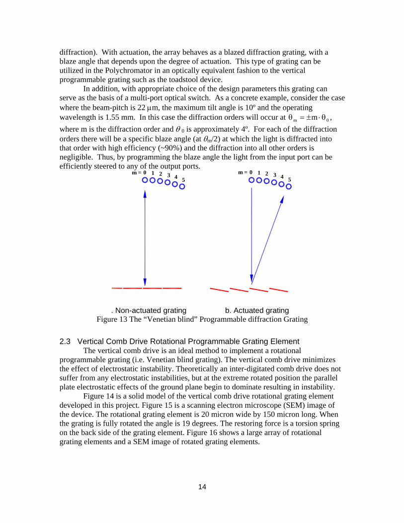
diffraction). With actuation, the array behaves as a blazed diffraction grating, with a blaze angle that depends upon the degree of actuation. This type of grating can be utilized in the Polychromator in an optically equivalent fashion to the vertical programmable grating such as the toadstool device.
In addition, with appropriate choice of the design parameters this grating can serve as the basis of a multi-port optical switch. As a concrete example, consider the case where the beam-pitch is 22 μm, the maximum tilt angle is 10º and the operating wavelength is 1.55 mm. In this case the diffraction orders will occur at , where m is the diffraction order and θ
0m m θ⋅±=θ
0 is approximately 4º. For each of the diffraction orders there will be a specific blaze angle (at θm/2) at which the light is diffracted into that order with high efficiency (~90%) and the diffraction into all other orders is negligible. Thus, by programming the blaze angle the light from the input port can be efficiently steered to any of the output ports.
m = 0 1 2 3 4 5m = 0 1 2 3 4 5
m = 0 1 2 3 4 5m = 0 1 2 3 4 5
. Non-actuated grating b. Actuated grating Figure 13 The “Venetian blind” Programmable diffraction Grating
2.3 Vertical Comb Drive Rotational Programmable Grating Element The vertical comb drive is an ideal method to implement a rotational programmable grating (i.e. Venetian blind grating). The vertical comb drive minimizes the effect of electrostatic instability. Theoretically an inter-digitated comb drive does not suffer from any electrostatic instabilities, but at the extreme rotated position the parallel plate electrostatic effects of the ground plane begin to dominate resulting in instability. Figure 14 is a solid model of the vertical comb drive rotational grating element developed in this project. Figure 15 is a scanning electron microscope (SEM) image of the device. The rotational grating element is 20 micron wide by 150 micron long. When the grating is fully rotated the angle is 19 degrees. The restoring force is a torsion spring on the back side of the grating element. Figure 16 shows a large array of rotational grating elements and a SEM image of rotated grating elements.
14

Figure 14 Solid model of a Rotational Vertical Interdigitated Comb Drive Grating
Element in a Actuated Position.
Figure 15 Scanning Electron Microscope Image of the SUMMiT™ Rotational
Programmable Grating Element. The MMPOLY4 mirror surface has been remove on the front grating element to enable visualization.
a. Large Array of Rotational Grating Elements b. Rotated Array Elements Figure 16 SUMMiT™ Rotational Programmable Grating Element Array
Figure 17 shows the rotation angle versus voltage curve for the rotational grating element. This device is fully rotated to 19 degrees at 60 V. Electro static instability occurs at 15 degrees which causes a hystersis loop between 15 and 19 degrees. A change of slope of the angle versus voltage curve occurs at approximately 11 degrees, due to the meshing of the fixed and rotational combs. Meshing of the interdigitated combs causes a
15

change in the derivative of the capacitance versus theta, θ∂∂C . This effect is beneficial since it delays the onset of electrostatic instability.
Electrostatic instability
Electrostatic Latching
Figure 17 Voltage – Rotation Angle Curve for the SUMMiT™ Rotational Programmable
Grating Element Array.
3 A New Optical Configuration for the Polychromator As originally envisioned, the Polychromator chip acted as a holographic element whose first-order diffraction efficiency spectrum was used to achieve the desired spectral transfer function of the correlation radiometer. While this approach has been successfully demonstrated, it suffers from a relatively low optical throughput, particularly for complex, multi-line spectra. We have demonstrated in the laboratory a new optical configuration for the Polychromator that addresses this shortcoming and greatly increases the overall optical throughput without degrading any other aspect of system performance [8]. In the new mode of operation, the programmable Polychromator grating is utilized in a fashion analogous to a spatial light modulator, Figures 18 and 19. Incoming infrared radiation is first collimated using a slit and converging lens. The collimated light is then directed onto a conventional high-efficiency diffraction grating that disperses the infrared wavelengths. A telecentric optic then projects a spectrally dispersed image of the input slit at the plane of the Polychromator chip. In the unactuated state, the Polychromator simply acts as a mirror that returns all the infrared energy through the optical system to the detector (a small vertical tilt is applied to the Polychromator to allow separation of the incoming and outgoing optical beams). Alternatively, the Polychromator can be actuated with deflection profile that will cause a portion of the infrared radiation to be diffracted into the +/- first order. The optical path followed by these diffraction orders does not return to the detector. Thus, the amount of infrared energy reaching the detector is decreased by the amount that was diffracted into the +/- first orders. If the relative displacement of the alternating beams is adjusted complete cancellation of the reflected wave can be achieved. Analog control of the amount of reflected energy can be achieved by using intermediate beam displacements. Since the incoming infrared wavelengths are dispersed along the length of the Polychromator chip, the magnitude of the beam
16
displacement at the location of any of the wavelengths incident on the Polychromator controls the optical throughput at that wavelength. In this fashion, any desired spectral transfer function can be achieved.
The throughput of the new optical system is limited only by the optical efficiency of the conventional blazed grating used to disperse the wavelengths. Optimized gratings can be obtained with efficiencies in excess of 80%, for a double pass throughput in excess of 60%. Even higher efficiencies are possible through the use of prism-based dispersive elements. Thus, high efficiency can be obtained for all the peaks in the spectral transfer function, regardless of the complexity or number of peaks.
Three other advantages are associated with the new optical configuration. First, the maximum beam deflection required from the MEMS chip is reduced by a factor of two. In the old, holographic mode of operation, the maximum beam displacement required corresponded to a full wave of phase shift (a 5 μm displacement gives a full wave of phase shift for operation at 10 μm wavelengths). In the new optical configuration the maximum phase shift required corresponds to a half-wave of phase shift (2.5 μm of displacement for 10 μm spectral wavelengths). The reduction of the maximum required beam deflection greatly simplifies the design and fabrication of the MEMS devices. The second advantage of the new configuration is a significant simplification of the control algorithms required to achieve a desired spectral profile. In the holographic mode of operation, sophisticated phase-retrieval algorithms were required to determine the positions of each of the beams on the MEMS chip. In the new mode of operation, there is a one-to-one correspondence between the wavelength and the position along the chip. In addition there is a one-to-one correspondence between the deflection amplitude and the degree of attenuation. Thus, the programming of the chip is extremely simple in the new configuration. The third advantage arises from the fact that only every-other beam needs to be actuated in the new scheme. This will decrease the number of voltages and interconnects required to operate the device by at least a factor of two.
17

Polychromator
TelecentricFocusingTelescope
TraditionalBlazed Grating
Detector
Beam Splitter
Slit
IR Source
Collection Lens
Figure 18 A diagram of the new, high-throughput optical system for Polychromator-based correlation radiometry
thro
ughp
ut
wavelength
λmin λmax
transfer function
beam profile
Figure 19 A schematic of a beam deflection profile and its corresponding spectral
transfer funcion.
18

Conclusion The main objective of this LDRD project was to develop a programmable gating
element for the Polychromator in the SUMMiT V™ surface micromachine fabrication process which meet the following objectives. • Vertical deflection of 6 µm of very narrow 20 micron wide gratings elements. • Analog control of the grating element over most of its operating range. • Residual stress induced deflections of the un-actuated and actuated structures must
be minimized (< λ/20). • Actuation voltage of the devices must be minimized to enable future integration of
control electronics (< 60V). • Repeatable analog control of the grating position.
Vertical and rotational grating elements were developed in this project. The vertical grating element utilizing compound leveraged bending was demonstrated to have a vertical deflection of 3.5 micron at 60 V. A rotational grating element utilizing vertical combdrive actuation was demonstrated to rotate to 19 degrees at 60 V. This work resulted in two technical advances and one patent application. Also a new optical configuration for the Polychromator was developed which increased the system optical efficiency. This new optical configuration relaxed the displacement requirements for the grating elements of the Polychromator, which allows both the vertical and rotational SUMMiT™ grating elements to be used.
Acknowledgements Thanks to Jerry Walraven for failure analysis of devices, Jeffrey Dohner for finite-element modeling, David Luck for device testing, Sita Mani for input on fabrication issues, David Adams of metallization expertise. In addition, we thank the Microelectronics Development Laboratory staff for fabrication of the SUMMiT™ devices.
References 1. R. Goody, “Cross-Correlating Spectrometer,” J. Opt. Soc. Am., 58, pp. 900—908
(1968) 2. M. B. Sinclair, M. A. Butler, S. H. Kravitz, W. J. Zubrzycki, A. J. Ricco,
“Synthetic Infrared Spectra”, Optics Letters, Vol. 22, No. 13, July 1 1997. 3. G. B. Hocker, D. Youngner, E. Deutsch, A. Volpicelli, S. Senturia, M. Butler, M.
Sinclair, T. Plowman, A. J. Ricco, The Polychromator: A Programmable MEMS Diffraction Grating for Synthetic Spectra, Solid-State Sensor and Actuator Workshop, 2-8 June 2000.
4. S. D. Senturia, E. S. Hung, “Extending the Travel Range of Analog-Tuned Electrostatic Actuators”, JMEMS, Vol. 8, No. 4, December 1999.
5. D. M. Burns, V. M. Bright, Development of microelectromechanical variable blaze gratings, Sensors and Actuatiors, A 64, pp. 7-15, 1998.
6. H. Xie, G. K. Fedder, Vertical comb-finger capacitive actuation and sensing for CMOS-MEMS, Sensor and Actuators, A 95, pp. 212-221, 2002.
19

7. H. Wada, D. Lee, U. Krishnamoorthy, S. Zappe, O. Solgaard, Process for High Speed Micro Electro Mechanical Systems (MEMS) Scanning Mirrors with Vertical Comb Drives, Jpn. J. Appl. Phys., Vol. 41, Part 2, No. 8A, pp. L899-L901, 1 August 2002.
8. M. B. Sinclair, K. B. Pfeifer, Stand-Off Chemical Sensing Using MEMS-Based Correlation Radiometry, Proceedings of the Standoff Detection for Chemical and Biological Defense Conference, Williamsburg, VA, October 25-29, 2004.
20

Distribution: 1 MS0123 D. L. Chavez, LDRD Office 01011 1 MS1080 D. R. Sandison 01769 1 MS1425 S. A. Casalnuovo 01744 1 MS0889 J. S. Custer 01851 1 MS1080 J. J. Allen 01769 1 MS1425 K. B. Pfeifer 01744 1 MS1411 M. B. Sinclair 01851 1 MS9018 Central Technical File 8945-1 2 MS0899 Technical Library 9616
21