advanced materials characterization project - nims material characterization project team is...
TRANSCRIPT

April
2014
3No.
Advanced Materials Characterization Project
W h a t c a n w e visualize?

02 NIMS NOW International 2014 April
A super-resolution electron microscope has made it possible to accurately examine even atomic ar-rangements. This is a critical technological advancement in terms of moving basic research forward.
Material researchers are ambitious—they seek to observe and measure various materials more accu-rately, in fi ner detail, and under special conditions. They want to know about the structure and proper-ties of new materials. These ambitions drive the advancement of characterization technologies and there is no end to this evolution. New characterization technologies allow material researchers to step into unknown territories of materials science.
Material researchers endeavor to visualize details with accuracy and visualize things which no one has seen before. NIMS’s project for the development of advanced materials characterization technologies provides cutting-edge measurement and analysis technologies that enable material researchers to carry out advanced material studies.
Advanced Materials Characterization Project
W h a t c a n w e v i sua l i ze?

03NIMS NOW International 2014 April

DoProcessing
PlanDesign
DoFabrication
DoSynthesis
Creation of novel material
Particulate processCreation of innovative
light material
Simulation of new material design
Advanced material characterization
technology
Organic molecules network
Material fabrication
SeeAnalysis
NIMS NOW International 2014 April04
Significance of advanced characteriza-tion technologies to characterize mate-rials: Plan-Do-See cycle
Based on NIMS’s third mid-term plan (2011-2015), we, the research team in the Advanced Key Technologies Division, are currently work-ing on the “development and application of ad-vanced characterization technologies,” which is one of five projects assigned to our division. The Advanced Key Technologies Division car-ries out research and development of advanced core technologies which are often needed for various material studies performed across the NIMS organization. Such technologies include those that allow comprehensive characteriza-tion of materials from the surface to inside (the “See” step of the cycle), simulation technologies for analyzing physical properties of materials and for estimating and designing purposes (the “Plan” step of the cycle), and synthesizing, nano-fabrication and processing technologies for producing materials from basic structural units (e.g., particles and organic molecules) (the “Do” step of the cycle). We are aiming to develop a common platform that will facilitate efficient material studies by us-ing the framework of the Plan-Do-See cycle and by creating a feedback circuit that will encourage collaboration between researchers (Fig. 1). The “See” part of the Plan-Do-See cycle, repre-sented by measurement technologies, plays a vital role in material studies. For example, the development of a super-resolution electron mi-croscope enabled accurate observation of the atomic arrangement structure in materials, which was nearly impossible before. The acqui-sition of such structural information has allowed
computational scientists to estimate electronic states and functional properties of a given ma-terial. In addition, nano-scale observation and mea-surement of various structures and properties of new materials in an actual operation environ-ment (i.e., active nano-characterization) allow material researchers to create and optimize new nano-processing technology[1]. Some research-ers believe that advanced measurement and analysis technologies will lead to new discover-ies[2]. And these technologies literally demon-strate the saying, “Seeing is believing.” Further-more, since these technologies lead to the creation of new materials, we would also add that these technologies demonstrate, “Seeing is creating.”
Mission and concept behind NIMS’s advanced characterization technologies
The mission of NIMS’s project for the develop-ment and application of advanced material char-acterization technologies is to develop such technologies that will meet the social needs and to use them for the creation of novel materials. We provide support for NIMS to maintain its com-petitiveness and capacity to carry out basic re-search for the development of environment and energy materials as well as next-generation infor-mation communication materials which have high social demand. Novel functions of new ma-terials are attributed to the structure, composi-tion, arrangement, and electron and spin states in surfaces, interfaces and bulk materials. Based on this view, scientists are attempting to under-stand the basic mechanisms behind the novel functions at an atomic level and in multiple-scale
studies. In order to meet the social demand and expectations, it is vital for us to develop a plat-form that will support world-class and compre-hensive studies on advanced material character-ization and provide it to interested researchers. To prepare such platform, we will need to combine material evaluation methods such as surface sen-sitivity and bulk sensitivity studies, assessments of single crystallinity and amorphousness, and nanoscale and macroscale studies. From this viewpoint, NIMS’s advanced charac-terization project team set up the following six subthemes based on the key concepts of com-prehensiveness and complementariness.
(1) Development and application of advanced technologies for the characterization of sur-face sensitivity(Daisuke Fujita, Nano Characterization Unit, Sur-face Characterization Group)(2) Development and application of advanced technologies for surface analysis(Shigeo Tanuma, Nano Characterization Unit, Surface Chemical Analysis Group)(3) Development and application of cutting-edge electron microscopy technology(Koji Kimoto, Surface Physics and Structure Unit, Electron Microscopy Group)(4) Development and application of charac-terization technology for high field nuclear magnetic resonance (NMR)(Tadashi Shimizu, Nano Characterization Unit, High Field NMR Group)(5) Development and application of charac-terization technology for strong neutron beams(Hideaki Kitazawa, Quantum Beam Unit, Neu-tron Scattering Group)
Division Director, Advanced Key TechnologiesUnit Director, Nano Characterization Unit
Daisuke Fujita
Advanced Characterization Technologies for Realization of Unknown Properties: Key Technologies that Facilitate Innovation
Project Collaboration: Plan-Do-See Cycle
Key technologies that support advanced research to develop novel materials
Fig. 1 Collaborative work in the framework of the Plan-Do-See cycle conceptualized in the mid-term project plan by the Advanced Key Technologies Division.
Fig. 2 Organization and objectives regarding the development and application of advanced material characterization technologies in NIMS’s mid-term plan.
Aiming to develop a world-class hub research institute for studies on advanced material characterization
Advanced material characterization project
Research organizationOutermost surface to outer layer to inner structure, amorphous to single crystal, static to dynamic, diverse environments
Surface sensitivity
measurement
Semiconductors Solar batteriesRechargeable
batteries Photocatalysts Fuel cells Spintronics
Advanced surface analysis
Advanced electron
microscope
Nano characterization
of outermost surface Live measurement
using X-ray
Light-element magnetism
AmorphousBulk / interface
High-speed time-resolved measurement
Analysis of three-dimensional
nanoscale surface
Advanced nano characterization and neutron beam
High field solid state NMR
Strong neutron beam
Synchrotron radiation analysis
Comprehensive and complementary
Development technologies
Output
What can we visual ize?Advanced Materials Characterization Project

05NIMS NOW International 2014 April
(6) Development and application of advanced characterization technology using synchro-tron radiation(Kenji Sakurai, Quantum Beam Unit, X-Ray Phys-ics Group)
We are aiming to support the development and application of advanced characterization technologies that will meet diverse needs of so-ciety and to develop a world-class hub research center (Fig. 2).
Advanced measurement technologies that accelerate innovation
The importance of innovative characterization technologies is well recognized in industrialized western countries. For example, the National In-stitute of Standards and Technology (NIST), in the United States, concluded that the advancement of characterization technologies is vital based on its comprehensive study on the measurement systems present in the U.S., and presented some specific cases illustrating that slow advancement in characterization technologies is a barrier to in-novative work in diverse industrial fields[3]. Ac-cording to a survey by the National Institute of Advanced Industrial Science and Technology concerning the global competitiveness of ana-lytical instrument industries, Japan is in second place in terms of global market share (14%) after the United States (66%). However, Germany, which is currently in third place with 13% share, is rapidly catching up with Japan[4]. In both the U.S. and Germany, their national governments are leading the development of advanced character-ization instruments and are also promoting the wide use of such technologies. Similarly, we as an incorporated administrative research institute should lead the high-risk de-velopment of advanced characterization tech-nologies. Based on this perspective, NIMS’s ad-
vanced material characterization project team is developing world-class technologies for core competence in line with the subthemes listed above. Some of the examples are shown in Fig. 3. We are developing world-class measurement technologies such as a multiple-extreme condi-tion scanning tunneling microscope, an elec-tron microscope capable of analyzing a single atom with 50-picometer spatial resolution, high field solid state NMR, and a de facto standard system that allows three-dimensional visualiza-tion of crystals and electron structures.
Promotion of sharing, standardization and further contribution to society
We as innovators of characterization technolo-gies are aiming to create a platform which will facilitate the wide use of such technologies we have developed. By making these measurement instruments available for shared use by research-ers, engineers and students regardless of their affiliation, we hope to facilitate more innovations, encourage the development and wider use of such instruments, and provide training to pro-spective researchers. Many of our team members taking part in NIMS’s advanced material charac-terization project are also participating in the mi-crostructural analysis platform project sponsored by the Ministry of Education, Culture, Sports, Sci-ence and Technology, making use of our ad-vanced nanomaterial characterization facilities. By doing so, they are making our advanced char-acterization facilities available to researchers across Japan. Furthermore, in order to promote the global use of those technologies, we are pro-moting international standardization which is vi-tal to facilitate collaborative research by working with such organizations as the International Or-ganization for Standardization (ISO)1) and the Ver-sailles Project on Advanced Materials and Stan-
dards (VAMAS)2). We are also taking initiatives to meet the needs of local communities. We have been publicizing air radiation dose information measured at three different NIMS properties in Tsukuba City since 2011. In addition, by holding open seminars, we are striving to provide accurate information on radiation measurements and decontamination, which local communities and local government staff are particularly interested in. Furthermore, to widely communicate our research results and train prospective researchers, we hold sympo-siums and international meetings on advanced characterization technologies in cooperation with researchers both in Japan and overseas (Fig. 4). As we described above, we have been develop-ing a hub research center for studies on advanced material characterization technologies with our mission being to prepare a common research platform, work on international standardization, contribute to society, and train prospective re-searchers, in addition to our fundamental mission to develop advanced characterization technolo-gies. We would like to use our facilities for diverse purposes.
[1] Fujita, D. 2002. Intellectual platform for active nano-characterization. Materia Japan. 41: 623-627.
[2] Nihei, Y. 2011. Characterization analysis technologies facilitate revealing new properties. NIMS Now. 11 (1).
[3] National Institute of Standards and Technology (NIST). 2007. An Assessment of the United States Measure-ment System: Addressing Measurement Barriers to Accelerate Innovation. NIST Special Publication 1048.
[4] National Institute of Advanced Industrial Science and Technology (AIST). 2011. Strengthening Japanese ana-lytical instrument industries in global competition. AIST study report.
1) ISO (International Organization for Standardization): a non-governmental organization that sets up interna-tional standards for industries.
2) VAMAS (Versailles Project on Advanced Materials and Standards): an international joint research scheme for pre-standardization.
ProfileDaisuke Fujita Doctor of Engineering. After completing a master’s program at the School of Engineering, the University of Tokyo, in 1986, worked as a research associate at the Institute of Industrial Science, the University of Tokyo. Has worked at the National Research Institute for Metals (NRIM; currently NIMS) since 1991. Became a unit leader in 1999 at the Extremely-High Vacuum Station. Became a sub-leader at the NIMS Nanomaterials Laboratory in 2001. Became a director at the Advanced Nano Characterization Center in 2006. Became a nanotechnology field coordinator in 2010. Assumed the current position as the director of the Advanced Key Technologies Division in 2011.
Fig. 3 Examples of world-class technologies for core competence that were developed during the advanced material characterization project.
Fig. 4 Our initiatives to meet social needs: regular publication of air radiation doses measured in three NIMS properties in Tsukuba City; holding of open seminars on the measurement of ra-diation; and holding of symposiums and international meetings on advanced characterization technologies.
Open seminar on the measurement of radiation

NIMS NOW International 2014 April06
Yasushi Yamauchi Doctor of Engineering. Completed the graduate program at Osaka University in 1985. Joined NIMS in the same year. Currently studying surface spin after some experiences on ion beams, fusion reactor walls and X-ray computed tomography. / Mitsunori Kurahashi Doctor (Engineering). Chief researcher. Completed the graduate program at Kyoto University in 1996. Joined NIMS in the same year. Areas of expertise: surface science, magnetism, development and application of state aligned molecular beams. / Han Zhang Ph.D. Researcher. After graduating from Tsinghua University, completed the graduate program at the University of North Carolina in 2006. Assumed the current position at NIMS in 2013 after working as a JSPS (Japan Society for the Promotion of Science) researcher and an ICYS (NIMS International Center for Young Scientists) researcher. Currently studying nanowires and high-brightness electron beam sources.
Profile
Group Leader, Spin Characterization Group, Nano Characterization Unit, Advanced Key Technologies Division
Yasushi Yamauchi
Spin Characterization Group, Nano Characterization Unit, Advanced Key Technologies Division
Mitsunori Kurahashi
Spin Characterization Group, Nano Characterization Unit, Advanced Key Technologies Division
Han Zhang
Spin Detection of Monoatomic Surface Layers
Ultimate surface sensitivity enabled by slow atomic beams
A helium (He) atom has two electrons. When a metastable He atom, in which one of these electrons is excited to the higher energy state, impinges on the material surface, the electron with higher energy (about 20 eV) will be eject-ed. By keeping the He atom’s kinetic energy level low down to a thermal energy level below 0.1 eV equivalent to that of helium gas in bal-loons, the He atom will rebound several ang-strom outside of the material surface and will not penetrate the surface layer. Due to this phenomenon, electrons ejected by a slow metastable He atomic beam irradiation of the material surface, gain information from the outermost surface layer only and thus they provide an ultimate “surface-sensitive property.”
Electron spin in the outermost nickel layer
By selecting metastable He atoms, in which all spins of their paired electrons are aligned in the same direction, you can identify the spin direc-tion (either upward or downward direction) of the surface electrons since only the surface elec-trons having the spin direction opposite to that of the He electrons interact with the He electrons (according to the Pauli exclusion principle). The upper graph in Fig. 1 depicts spin asym-
metries calculated by the formula, (Ip-Ia)/(Ip+Ia), where Ip and Ia represent intensities of elec-trons ejected from the clean surface of Nickel (Ni), a kind of permanent magnet, during a metastable He atomic beam irradiation with the parallel and antiparallel spin to that of the total Ni electrons (i.e., majority spin).[1]
Because of the fact that interacting surface electrons and the electrons of metastable He at-oms have to have spins in opposite directions to each other, the positive spin asymmetry at the Fermi level of 13.5 eV indicates that the spin di-rection of the surface electrons tends to be op-posite to the majority spin (polarization). This spin reversal is normally found in ferromagnetic transition metals and accordingly, the electrons that pass through Ni are also polarized toward the opposite spin direction with respect to the majority spin.
Electron spin reversal in graphene monoatomic layer
A clean Ni surface was then exposed to benzene vapor to grow a graphene monolayer which has the appearance of a honeycomb consisting of hexagonal carbon atoms. The lower graph in Fig. 1 shows the resultant spin asymmetry ratios.[1] At 14-15 eV, which is close to the Fermi level, the spin asymmetries are negative, indicating that by coating the Ni substrate with a graphene mono-layer the surface spin is reversed and that the sur-
face electrons are polarized in a direction consis-tent with the majority spin. These results have revealed for the first time that the contact of graphene with Ni causes spin polarization of the electron, which is rele-vant to electrical conduction but which origi-nally shows no spin polarization. The theoretical calculations presented in Fig. 2 also support these results.[2]
Development of high-precision state control technology
In this project, we are also developing molecu-lar beams which are aligned in a single quantum state concurrently with the development of atomic beams. We have already developed oxy-gen molecular beam technology in which the direction of the molecular axis and spin can be specified. Using this technology, we have been able to resolve the decades-long mystery of the dynamics in aluminum oxidation reaction.[3] In addition, we are currently developing technolo-gies for low energy fine-focused electron beams and observation of the spatial distribution of electronic spin in the outermost surface layer.
[1] S. Entani, M. Kurahashi, X. Sun and Y. Yamauchi, CAR-BON 61. (2013). 134.
[2] X. Sun, S. Entani, Y. Yamauchi, A. Pratt and M. Kura-hashi, J Appl. Phys. 114. (2013). 143713.
[3] M. Kurahashi and Y. Yamauchi, Phys. Rev. Lett. 110. (2013). 246102.
Fig. 2 Cross-sections of spin density distribution based on the first principle calculation. Blue areas represent the polarization of Ni toward the majority spin, while red areas stand for the opposite. At around the Fermi level (right), the electrons orbiting around the nuclei of carbon atoms (C) in graphene are polarized parallel to the majority spin of Ni. In contrast, at the lower level (left), the electrons orbiting around the nuclei of Ni are polarized antiparallel.
Fig. 1 Kinetic-energy-dependent spin asymmetries of electrons ejected from the surfaces of Ni (upper graph) and a graphene monolayer grown on it (lower graph).
Fermi level
What can we visual ize?Advanced Materials Characterization Project
07NIMS NOW International 2014 April
Hideki Yoshikawa Ph. D (Engineering). Completed his graduate study at Osaka University in 1992. Joined the National Institute for Research in Inorganic Materials (NIRIM; currently NIMS) in 1995. Specializes in X-ray photoelectron spectroscopy and electron scattering simulation. / Sei Fukushima Ph. D (Engineering). Completed his graduate study at the University of Tokyo in 1986. Joined NIRIM in 1994. Specializes in state analysis via inner shell electron theory, X-ray photoelectron spectroscopy. / Shigeo Tanuma Ph. D (Science). Completed the doctoral course at the University of Tsukuba, Department of Chemistry in 1982. Joined NIMS in 2001. Director of the Research Network and Facility Services Division, Leader of the Surface Chemical Analysis Group, and Director of the Materials Analysis Station as of March 2014. Specializes in surface analysis, surface electron spectroscopy. / Kunie Ishioka Ph. D (Science). Became NRIM Researcher in 1994 and has held the office of Principal Researcher since 2006. Specializes in ultrafast semiconductor spectroscopy.
Profile
Group Leader, Surface Chemical Analysis Group, Nano Characterization Unit, Advanced Key Technologies Division
Hideki Yoshikawa
Surface Chemical Analysis Group, Nano Characterization Unit, Advanced Key Technologies Division
Sei Fukushima
Surface Chemical Analysis Group, Nano Characterization Unit, Advanced Key Technologies Division
Shigeo Tanuma
Surface Characterization Group, Nano Characterization Unit, Advanced Key Technologies Division
Kunie Ishioka
Observation of Dynamic Behavior of Electrons in a Material— Development of New Technology for Chemical State Analysis —
Observation of chemical bonding in a material by detecting electrons excited by various wavelengths of light
The chemical bonding of atoms in a material is created by valence electrons. Observing the dy-namic transitions of electrons between their energy levels enables us to ascertain the chemi-cal bonding and its origin by which material is characterized. Furthermore, clarifying the chemical bonding states of various materials is essential for developing materials and improv-ing the performance of new devices. Photo-irradiation is commonly used as a probe to observe the behavior of electrons in a mate-rial because photons excite electrons in the ma-terial more directly than any other probes and enables energy-level selective excitation. We can extract electrons from a material into the vacuum by irradiating it with short-wave-length light (ultraviolet rays and X-rays), which has greater energy than visible light, and we can produce excited states of electrons within a ma-terial by irradiating it with long-wavelength light (visible light, infrared light, microwaves). The analysis of electrons extracted from a tar-get element within the material into the vacu-um by short-wavelength light enables to reveal the chemical bonding structure around target element, and observing the energy transfer
from electrons excited by long-wavelength light to the collective vibration of atoms (pho-nons) enables to reveal the direction and strength of chemical bonding in the material.
Nano-level depth-profile analysis using X-ray-excited photoelectrons
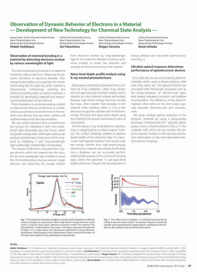
Observation of electrons extracted from a ma-terial by X-ray irradiation, called X-ray photo-electron spectroscopy, has been widely used in industry as a key chemical analysis technology. Because high-kinetic-energy electrons excited by X-rays, often transfer their energies to the material while traveling within it, only a few electrons escape the material with initial kinetic energy. This limits the observation depth using this method from several nanometers to tens of nanometers. For this reason, X-ray photoelectron spectros-copy is categorized as a surface analysis meth-od. The surface sensitivity enables to observe depth-profile of the chemical state of a nano-meter multi-layered material. If we closely study the energy transfer from high-kinetic-energy electrons to a material and compile the findings into a database, we can accurately perform depth-profile analysis of the chemical bonding state within the specimen in sub-nano-level depth resolution. It targets the development of
various devices with nano-level internal struc-tures (Fig. 1).
Ultrafast optical response determines performance of optoelectronic devices
In our daily life, we are surrounded by photonic materials, which work as photo-catalysts, solar cells, LEDs, lasers, etc. The optical functions are associated with microscopic processes such as the photo-excitation of electron-hole pairs, their energy relaxation, transport and radiative recombination. The efficiency of the photonic materials often relies on the time scales, typi-cally between femtoseconds and microsec-onds. We study ultrafast optical responses of the photonic materials by using a pump-probe technique. Femtosecond (10-15 second) optical pulses induce coherent phonons (Fig. 2) in the materials, with which we can monitor the col-lective atomic motions in the real time and ex-tract information on the time-dependent elec-tron-phonon coupling.
Fig. 1 The energy loss functions of gallium arsenide (GaAs) obtained in reflection electron energy loss experiments. When high-kinetic-energy electrons travel within a material, they cause collective excitations within the material. This phenomenon is called plasmon (the peak in the figure represents the plasmon of GaAs). It is a major factor that decelerates high-kinetic-energy electrons. Quantitative understanding of this phenomenon leads to precise estimation of the observation depth of X-ray photoelectron spectroscopy.
Fig. 2 The reflectivity of graphite is modulated periodically by coherent phonons (lower panel). The phonon frequency transiently upshifts upon photoexcitation (upper panel), revealing the electron-phonon decoupling in the two-dimensional system.

NIMS NOW International 2014 April08
Koji Kimoto Ph.D. (Science, Tohoku University). Completed the master's course in the Graduate School of Engineering, Nagoya University, in 1989, and joined Hitachi Research Laboratory, Hitachi, Ltd., in the same year. Became a Senior Researcher of the NIRIM (currently NIMS) in 1999. Also teaches at Kyushu University, since 2009, as a professor under the Joint Graduate Program with NIMS.
Profile
Electron Microscopy Group, Surface Physics and Structure Unit, Advanced Key Technologies Division
Koji Kimoto
Application of Advanced Electron Microscopy for Characterization of Various Materials
Microstructures and trace elements affect-ing macroscopic material characteristics
Superior material performance and characteris-tics of new materials are often determined by microscopic crystal structures or trace amounts of added elements. This is true not only for elec-tronic devices that are increasingly miniaturized such as semiconductor devices and magnetic disks, but also for functional materials such as fluorescent materials used for LEDs, or structural materials such as steel used for buildings. Macro-scopic characteristics of these materials, such as their luminescence property and mechanical strength, change dramatically by added ele-ments. By applying electron microscopy to iden-tify microstructures and trace elements that ex-hibit material functions, we can push forward development of high-performance materials even further. NIMS develops advanced measure-ment techniques using electron microscopy, and promotes research on material characteriza-tion in cooperation with internal and external material researchers including those from other research institutes and companies.
Cutting-edge electron microscopy
The minimum size of the structure that can be observed by electron microscopy (spatial resolu-tion) depends on the wavelength of the elec-trons (normally several picometers) and the ab-errations of the lenses used in the observation.
With a spherical aberration corrector that has been put to practical use recently, it is possible to observe materials by converging electrons to a size smaller than the atomic diameter (approxi-mately 0.1 nanometers). Since electrons entering a sample scatter through various interactions with atoms in the material, we can, for example, analyze elements and the chemical bonding state from the electron energy-loss upon the scattering. In addition, we can use the character-istic of electrons being both waves and charged particles to measure magnetic or electric fields.
Electron microscopy research at NIMS
Figure 1 shows the appearance of an electron microscope we currently use. In order to realize atomic resolution, the microscope is installed on an active anti-vibration system in a room with a panel air conditioner. Users operate the micro-scope from the next room separated by a dou-ble window. Spatial resolution of 50 picometers is achieved by using a spherical aberration cor-rector, and we can directly observe crystal struc-tures. Moreover, with energy resolution of 70 meV realized by a monochromator, we can ana-lyze the electronic structure and identify the va-lence and the coordination number of the con-stituent elements. We also develop software for experiments and analyses, and develop technologies for handling materials that alter with the slightest amount of moisture. The developed technologies are also
used for collaborations with external researchers through projects such as the NIMS Microstruc-tural Characterization Platform.
Example of advanced measurement
Here is one example of NIMS’s diverse material development and characterization efforts. Figure 2 shows an example of detection of euro-pium (Eu) in SiAlON, which NIMS has developed as a fluorescent material for LEDs. We can see that an Eu monoatom exists in a tunnel with a diameter of about 0.5 nanometers within the crystal structure. This result was obtained by using custom multiple measurement software and succeeding in detect-ing the slight signals generated by the monoatom. Figure 3 shows the result of observation of vortex-like microscopic magnetic domains called Sky-rmions by Lorentz microscopy.*) Observation of magnetic domains of a nanometer order is effec-tive for analyzing magnetic memory devices using electron spin as magnetic information. In this manner, we are currently advancing re-search and development of electron micro-scopes not as mere magnifying glasses, but as comprehensive tools for analyzing material char-acteristics.
* Lorentz microscopy: One of the measurement tech-niques of electron microscopy for observing micro-scopic magnetic domains by using a Lorentz force in the magnetic field.
Fig. 1 (a) Appearance of an electron microscope. Picture of a user operating the microscope from the next room is on the page 2-3.
Fi g. 3 ( a ) Exa mple o f observation of Skyrmions generated within FeGe by Lorentz microscopy. (b) Schematic of a Skyrmion.
Fig. 2 (a)Crystal structure of SiAlON fluorescent material. (b) The Eu monoatom dopant observed (pointed to by the arrow in the center); measured under accelerating voltage of 80 kV; the sample provided by Hirosaki (NIMS), et al.
What can we visual ize?Advanced Materials Characterization Project

09NIMS NOW International 2014 April
Tadashi Shimizu Doctor of Science. Assistant Researcher at The University of Tokyo, Institute for Solid State Physics from 1987. Joined NRIM in 1990, and current position from 2001.
Profile
Group Leader, High Field NMR Group, Advanced Nano Characterization Center
Tadashi Shimizu
Development of High Field Solid State NMR Technology and Its Application to Material Analysis
Efforts to promote the use of NMR tech-nology in inorganic material studies
NMR (nuclear magnetic resonance) is a well-established technology in organic chemistry and clinical medicine (e.g., magnetic resonance imaging or MRI) used in standard analytical in-struments. However, it is not a common tech-nology used in material research. In both organic chemistry and MRI, NMR signals from hydrogen are measured. The magnetic field strength used in organic chemistry is about 10T (tesla) and that used in MRI ranges from 1T (body parts other than the head) to 4T (brain). While these magnetic fields are relatively low given that superconducting magnets can generate higher magnetic fields, the demand for higher magnetic fields is generally low. That is because hydrogen is often the only element required to be mea-sured in organic chemistry and MRI. Because NMR signals from hydrogen are stron-ger than those from any other elements, they can be measured even in low magnetic fields. However, there is a problem with the applica-tion of NMR technology to material studies. Most inorganic materials in particular do not contain hydrogen, so if the technology is to be used in inorganic material studies, it will be nec-essary to measure NMR signals from other ele-ments that generate weaker NMR signals. Since the sensitivity and resolution of NMR signals in-crease in higher magnetic fields, the use of a suf-ficiently high magnetic field is necessary in or-der to accurately measure elements with weak NMR signals. In theory, NMR technology is applicable to about 80% of the elements in the periodic table. However, in reality, NMR signals from only a few
elements such as hydrogen had been measur-able due to the delayed progress in the devel-opment of high field magnets. Thus, NMR tech-nology had been useful only in limited research areas such as organic chemistry. The most effective method to expand the appli-cability of NMR technology is to use a high mag-netic field. While the strength of the magnetic fields used with common NMR analytical instru-ments is about 10T, the use of magnetic fields with strength greater than 20T helped achieve the first successful application of NMR technology to ele-ments which had been the least applicable, known as quadrupolar nuclei (i.e., atomic nuclei that have a nuclear spin quantum number greater than one), which account for about 60% of the elements in the periodic table (Table 1). Traditionally, it had been known that quadru-polar nuclei are extremely difficult to resolve us-ing NMR technology and that the use of a high magnetic field is technically the only solution to this problem. If the development of high field solid state NMR technology enables accurate measurement of quadrupolar nuclei, it would be applicable to a wide range of material stud-ies including those on inorganic materials. Since NMR technology has an advantage of being rather effective in the analysis of random struc-tures in amorphous materials, it is expected to work complementarily with conventional tech-nologies such as X-ray and electron microscopy.
World’s first successful high-resolution measurements of Ca, Mg, Ti and Mo in practical materials
Figure 1 shows a graph which compares the de-grees of difficulty in measuring NMR among quad-
rupolar nuclei. The dotted lines indicate the strength of the magnetic field necessary to ana-lyze NMR signals from a given element (i.e., ele-ments located closer to the lower right corner re-quire higher magnetic fields). Red circles indicate quadrupolar nuclei from which NMR signals have been successfully measured in the past five years using the 930MHz-NMR facility (using a 21.8T mag-netic field) which is in operation at NIMS. Notably, we succeeded for the first time in the world in high resolution measurement of NMR sig-nals from Ca, Mg, Ti and Mo in practical materials, which are among the most difficult elements to measure. NMR signals from these elements had been undetectable using the conventional facili-ties with magnetic field strength of about 10T. Although we can now measure NMR signals from those difficult elements, the measurement is time-consuming, requiring us to spend more than 100 hours duplication measurements. We spend the first several days of the experiment patiently choosing the proper parameters to use out of 20 parameters representing various measurement conditions. This process requires experience and insightful skills to perceive “vir-tual signals” and highly specialized knowledge. Solid state NMR technology applicable to quadrupolar nuclei has become available only recently after the invention of magnets that can generate 20T or higher fields. Since nearly no references or literature on this subject are avail-able, we feel like we are groping in the dark when working on this new technology on a daily basis. At the same time, we are excited to explore it. We hope to expand the applicability of solid state NMR facilities to measure various new substances and materials beyond their tra-ditional application in organic chemistry.
Ta b l e 1 . T h e s e n s i t i v i t y a n d resolution of dipole nuclei (blue) are directly proportional to the applied magnetic field. The sensitivity and resolution of quadrupolar nuclei (red and yellow) improve by raising the magnetic field strength to the second to fifth power. Since magnetic field strength of more than 20T is required to acquire high NMR resolution when applied to quadrupolar nuclei, the conventional NMR devices (with about a 10T magnetic field) were not useful in analyzing them. (T. Shimizu, et al., Chem. Lett. 33 (2004) 1502)
Fig. 1 A graph indicating the degrees of d i f f icult y in measuring NMR among q u a d r u p o l a r n u c l e i . T h e dotted blue lines indicate the extent to which NMR signals from elements are measurable in relation to magnetic field strength. Red circles indicate quadrupolar nucle i f rom which NMR signals had been successfully measured using a 930MHz-NMR facility. ( T. Shimizu, et al., Chem. Lett. 33 (2004) 1502)
(b)
Quadrupolar nucleiDipole nuclei
Relative resolution of quadrupolar nuclei
Easy
Difficult
Rela
tive
sens
itivi
ty o
f qua
drup
olar
nuc
lei

NIMS NOW International 2014 April10
Hideaki Kitazawa Completed the physics curriculum at the Graduate School of Sciences, Tohoku University, in March 1987. Employed as a researcher at the Institute of Physical and Chemical Research in April 1987. Became a chief researcher at the National Research Institute for Metals in 1995. Became a group leader at NIMS in April 2001. Assumed the current position in April 2011. Acquired doctoral degree in science in 1988. / Noriki Terada Completed the doctoral program in physics at the Graduate School of Science, Tokyo University of Science, in March 2006. Became a basic science special researcher at the Institute of Physical and Chemical Research. Assumed the current position in April 2007. Studied at the Rutherford Appleton Laboratory ISIS in the United Kingdom between August 2011 and February 2014 taking advantage of the JSPS (Japan Society for the Promotion of Science) program.
Profile
Unit Director, Quantum Beam Unit, Advanced Key Technologies Division
Hideaki Kitazawa
Neutron Scattering Group, Quantum Beam Unit, Advanced Key Technologies Division
Noriki Terada
Development of High-Pressure Cell to Neutron Scattering Experiments and Their application to Multiferroic Materials
Understanding physical properties of materials based on electronic states
Because neutrons, constituents of atomic nu-clei, possess high penetrability and great re-sponsiveness to light elements and spin states, the application of neutron beams to advanced materials reveals material’s internal structures such as composition, texture and various micro-scopic states (e.g., electronic, spin and chemical states) in a non-destructive way. We have been developing equipments that are able to create various multiple extreme environments (e.g., high pressure, low temperature and high mag-netic field) in order to understand important electronic states of materials.
Relationship between multiferroics and magnetic structure
Multiferroics that possess several strongly or-dered states (e.g., ferromagnetism [or antiferro-magnetism], ferroelectricity and ferroelasticity) not only exhibit unique and interesting physical phenomena but also indicate that magnetiza-tion and dielectric polarizationⅰ can be manipu-lated by electric field and magnetic field, re-spectively. Due to these properties, multiferroics are attracting the attention of researchers who develop devices such as new types of large scale memory devices. The delafossite CuFeO2 with a layered triangular lattice was studied at an early time as a model for frustrated magne-tismⅱ, and it has been studied extensively in
recent years as a multiferroic model after the discovery of magnetic-field-induced ferroelec-tric polarization1). As illustrated in Figure 1, magnetic frustration of CuFeO2 is released by spontaneously distorting its crystal lattice at low temperatures (i.e., its wave-number changes with temperature), and thereby the magnetic structure with the commensurateⅲ magnetic wave vector and without dielectric po-larization is realized. The commensurate magnet-ic state can easily change to a ferroelectric state with the incommensurate magnetic phase2) by means of impurity substitution. This suggests that commensurate states are extremely unstable, and there seems to be a strong relationship between the commensurate-incommensurate magnetic structure and ferroelectricity. In this research, we anticipate that magnetic struc-ture can be changed by applied pressure suppress-ing the spontaneous lattice distortion. We have de-veloped a hybrid anvil high pressure cell which allows us neutron diffraction experiments under high pressure. Recently we carried out neutron dif-fraction experiments using the high pressure cell.
High pressure cell for neutron diffraction experiments and magnetic structure under high pressure
The hybrid high pressure cell(Figure 2), which we developed with Dr. Toyotaka Osakabe of the Ja-pan Atomic Energy Agency for use in pulsed neu-tron diffraction studies, is not only capable of gen-erating high pressure but is also equipped with a
hybrid anvil cell consisting of SiC (silicon carbide) and WC (tungsten carbide) anvils, allowing the neutron beams detectable widely3). Convention-ally, it had been difficult to attain sufficiently large signal-to-noise ratios (S/N) due to scattered neu-trons from a high pressure region and we resolved this problem by greatly improving the S/N ratio using a BN (boron nitride) masking shield. As shown in Figure 1, we found that under high pressure at 7.9GPa (= 79,000 atmospheric pres-sure), CuFeO2 maintains an incommensurate magnetic structure even at low temperatures, which was not the case under 1 bar (= 1 atmo-spheric pressure)3
In other words, under high pressure, a frustrated magnetic ordered state is stably preserved at low temperatures. These results indicate that we might be able to ma-nipulate multiferroic properties by adjusting the pressure, as such manipulation was feasible when magnetic fields and chemical substitution were tuned. For future studies, we plan to carry out de-tailed neutron experiments under high pressure, aiming to reveal the mechanism behind the expres-sion of multiferroic properties under such conditions.
1) T. Kimura et al., Phys. Rev. B 73, 220401(R) (2006).2) N. Terada et al., Phys. Rev. B 78, 014101 (2008).3) T. Osakabe et al., J. Phys. Soc. Jpn.,79 034711 (2010).4) N. Terada et al., Phys. Rev. B 83, 020403(R) (2011).
ⅰ Dielectric polarization: It is also known as electric po-larization. Polarization of electric charge occurs when an electric field is applied to a dielectric material. Di-electric polarization that occurs in the absence of an external electric field is called spontaneous polariza-tion (or ferroelectric polarization).
ⅱFrustration: The strongest frustrated state occurs when spins of adjacent magnetic atoms on a triangular lattice interact so that their spins only align in opposite direc-tions each other (antiferromagnetic exchange interac-tion) as shown in the left diagram of Figure A. If the di-rection of spin 1 is arranged upward, the direction of spin 2 must become downward. Thereby the direction of spin 3 cannot choose either upward or downward directions (frustration). When the spin direction of each magnetic atom in the triangular lattice is allowed to ro-tate freely, the frustration state is partially weakened as shown in the right diagram of Figure A. This mechanism may lead to the emergence of ferroelectric polarization.
ⅲ Commensurate and incommensurate: If a period of a certain order is an integer multiple of the lattice con-stant, it is called commensurate. On the other hand, if the period is a non-integer multiple of the lattice con-stant, it is called incommensurate.
Figure A. Magnetic frustration with a triangular lattice
Fig. 2 Hybrid high pressure cell for neutron scattering experiments (diameter: 45mm, height: 77mm). (Left) Whole image of device. (Right) Close-up of a hybrid anvil part. The upper and lower anvils were made of tungsten carbide (black) and silicon carbide (light blue), respectively. The actual dimension of the specimen is about 0.5mm x 0.6mm x 0.25mm, and glycerin is used as a pressure medium.
Fig. 1 (a) Magnetic neutron diffraction patterns of CuFeO2 under the 7.9GPa pressure and at various temperatures. Magnetic reflection peaks with the incommensurate magnetic wave vector (ki=(0.192, 0.192, 3/2)) were observed in a wide range of temperatures between 3 and 20K. The inset
compares magnetic neutron diffraction patterns among different temperatures under 1 bar. The wavenumber indicates temperature dependence and the magnetic reflection peaks with the incommensurate magnetic wave vector ki shift to those with the commensurate magnetic wave vector (kc=(1/4, 1/4, 3/2)) at a low temperature of 4K. (b) Temperature dependence of the wavenumber and anticipated magnetic structures compared between 1 bar and 7.9GPa.
→
→
→
What can we visual ize?Advanced Materials Characterization Project

NIMS NOW International 2014 April
Kenji Sakurai Doctor of Engineering. Graduated from the Facility of Engineering, the University of Tokyo, in 1983. Completed the doctoral program at the University of Tokyo graduate school in 1988. Joined NRIM in 1988. Currently a leader at NIMS’ X-Ray Physics Group in the Quantum Beam Unit.
Profile
X-Ray Physics Group, Quantum Beam Unit, Advanced Key Technologies Division
Kenji Sakurai
Characterization of Buried Interfaces Using Synchrotron Radiation Measurement
Characterizing buried interfaces
It is a general practice in nanotechnology re-search and development to cover nanostruc-ture surfaces, which were fabricated under pre-cise control, in order to protect it from physical or chemical deterioration and damage. It is also common to create multilayered nanostructures. The properties and functions of the parts on the surface of the most interest, which are kept unexposed by covering the surface with a dif-ferent substance, have been studied and uti-lized. What is known as “buried interfaces” in-clude not only semiconductors, magnetic devices and thin films used of soft materials but also various coating interfaces, adhesive inter-faces, interfaces between two different sub-stances and solid-liquid interfaces that can be found in ecosystems, quasi-ecosystems and battery materials. Many advanced characterization and analytical technologies are becoming very useful in de-tailed analysis of atomic arrangements, molecu-lar-level structures and electronic states on ex-posed surfaces. However, it had been difficult to apply these technologies to buried interfaces.
Sophistication of X-ray reflectivity method
At NIMS, we have been developing the tech-nology called X-ray reflectivity and enhancing the analytical method to characterize the vari-ous kinds of interfaces mentioned above. Our first specific objective is to pioneer a mod-el-free analytical method which is effective in dealing with the case where the interface struc-ture is complex and thus difficult to understand in detail, the case where interfacial reaction might cause the production of an additional layer or the loss of an existing layer, and the case where analysis using a structural model is not very reliable. Accordingly, we have been plan-ning and implementing a new analytical meth-od which does not rely solely on fitting of struc-tural parameters to the data but instead uses transformation schemes such as the Fourier transform and wavelet transformation. Our second objective is to develop the tech-nology to form an image based on the distribu-tion of electron density at a certain depth in an interface (Fig. 1). In the field of medicine, X-ray computed tomography is frequently used to at-tain cross-sectional images of the brain and other internal organs in a non-destructive man-
ner. Similarly, we are developing a methodology to analyze internal structures buried under thin films and multilayer films using reflected X-rays rather than penetrating X-rays (patent applica-tion submitted). In addition, we found that white synchrotron radiation is also effective for this purpose (Fig. 2). Our third objective is to develop technology to track the changes in interfaces which continu-ously change. In order to identify the mecha-nism responsible for interfacial reactions and specific functions of interest, it is extremely im-portant to conduct real-time measurement of changing interfaces in addition to static mea-surement. Research and development activities to en-hance the abovementioned characterization and analytical technologies are expected to ad-vance greatly due to emerging tools such as a new source of ultra-low emittance synchrotron radiation and an X-ray free-electron laser that will become available soon. So in the near fu-ture, we expect to be able to characterize many interesting phenomena that occur in buried in-terfaces in detail and in a more direct manner.
Reference: Sakurai, K. (editor) 2009. Introduction to X-ray reflectivity. Kodansha Scientific Ltd, Tokyo, Japan.
(a)
(b)
(c)
(d)
Fig. 2 One-dimensional X-ray reflectivity scanning of Cr, Cu and Au line patterns fabricated on a glass substrate. Localized analysis of an interface can be achieved by identifying each line pattern through the continuous acquisition of X-ray reflectivity spectra at specified points while moving the sample material, using parallel and microfocus beams of high energy white X-rays.
Fig. 1 The upper diagram illustrates the mechanism behind the imaging of superficial and buried interfaces using X-ray reflectivity. This approach revealed that imaging of electron density distribution along the parallel direction of the interface at an intended depth can be achieved by first acquiring a strength profile of the reflected X-rays and then mathematically processing it to create a reconstructed image. The images and graphs in the right show the results concerning the pattern of gold coating on a silicon surface. (a) Image of gold coating pattern observed using an optical microscope, (b) Line profile corresponding to the image in (a), (c) Reconstructed image based on X-ray reflectivity projection data, and (d) Line profile corresponding to the image in (c).
Synthetic
quartz glass
substr
ate
X-ray energy (keV)
X-ra
y st
reng
th (c
ount
s)
Position sensitivedetector
Sample material
X-ray source

On March 10, NIMS and Southeast Univer-sity (SEU) in China concluded memoran-dum of understanding (MoU) for interna-tional collaboration which is for design of graphene based materials as new platinum free electro-catalysts and development of high quality fuel cell electrodes. SEU located in Nanjing is one of the oldest institutions of high education and scientific research in China. Its origin can be traced back to 1902. The university boasts over 34 schools or de-partments with 64 undergraduate disci-plines in all, which offers 98 Ph.D. programs
and 208 Master programs. The total number of faculty and staff is 6,000, including 1,300 full or associate professors. A key person of SEU side is Prof. Yuanjian Zhang who spent some important years in NIMS as a young scientist. After the MoU ceremony, Prof. Zhang talked his recent work in his seminar to strengthen the tie of both institutions. Since NIMS is located in Tsukuba city, Tsuku-ba University will join this international col-laboration team. It is expected that afore-mentioned research team will create lots of outcomes to develop the high quality elec-
trodes in fuel cell and contribute to the ma-terials science in both countries.
Dear NIMS NOW readers, I was born in Indonesia and moved to New Zealand when I was 14 years old. I am very blessed to have two wonderful countries in
which I can call home. After finishing my PhD study from The University of Auckland, I started working as a postdoctoral re-searcher in Toyohashi University of Tech-nology, Japan in May 2010. A year after that, I got offered a position in the Photovoltaic Materials Unit of NIMS. Working at NIMS is very exciting. I truly enjoy the diversity in NIMS. Not only that I get to learn from the talented Japanese researchers, but also I have the opportunity to work with many international researchers. Research facilities are superb and definitely world-class. NIMS is located in Tsukuba city, which is a very comfortable place to live and it is only one hour away from the excitements of Tokyo. Living in Japan is an amazing experience. Japan is such a beautiful country that is rich
in culture with very friendly and down-to-earth people. I am so thankful for this op-portunity.
Hello NIMS
Noviana Tjitra Salim(Indonesia)Period of Stay at NIMS: 2.5 yearsPostdoctoral researcher, Photovoltaic Materials Unit
On April 22, Her Highness Sheikha Moza bint Nasser, Chairperson of Qatar Founda-tion for Education, Science and Communi-ty Development (QF) visited NIMS on the occasion of her visit to Japan. Her Highness was accompanied by His Excellency Mr. Yousef Mohamed Bilal, Qatar’s Ambassador to Japan and a high-level scientific delega-tion, including President of QF Research and Development Mr. Faisal Alsuwaidi and Executive Director of the Qatar Environ-ment and Energy Research Institute (QEERI),
Dr. Mohammad Khaleel. Her Highness and the delegation received a presentation about NIMS and its work in the filtering and purification of water research, and the su-percomputer, K computer. Her Highness had a discussion with President Prof. Ush-ioda and executives regarding bilateral re-search collaboration. Both sides explored potential synergies in materials technology for energy and environment issues be-tween NIMS and QF, especially QEERI. The meeting concluded with the signing cere-
mony of a Memorandum of Understanding to encourage joint research activities.
MoU with Southeast University in China for fuel cell electro-catalysts and electrodes
Consort of the Father Emir of the State of Qatar, Her Highness Sheikha Moza Visits NIMS
1
2
Sakura season, Tsukuba city.
Climbing Mt. Fuji, the tallest mountain in Japan.
2014 No.3
NIMS NOW International 2014 vol.12 No.3
cover image:Very Low Temperature, High Magnetic Field Scanning Tunneling Microscope.
Participants at the signing ceremony (from top left): Dr. Mori, Prof. Liu, Prof. Sun, Prof. Zhang, Dr. Takada.
group photo.