advanced materials: challenges and opportunitiestechdigest.jhuapl.edu/td/td2104/rooney.pdf ·...
TRANSCRIPT

M. ROONEY ET AL.
516 JOHNS HOPKINS APL TECHNICAL DIGEST, VOLUME 21, NUMBER 4 (2000)
N
Advanced Materials: Challenges and Opportunities
Michael Rooney, Jack C. Roberts, George M. Murray, and Bruce M. Romenesko
ew materials, or new ways of using and combining existing materials, are beingrequired to meet tomorrow’s engineering applications. This need is compounded bypressures to stay competitive by keeping costs reasonable while continuing to make newmaterial technologies available to our APL customers. The main challenges created bytoday’s environment include the understanding and assimilation of the rapid techno-logical advances being made by industry, the integration and application of theseadvances to APL customer needs, and preparation for the next set of requirements andapplications made possible by maintaining a leading technical edge. The TechnicalServices Department is helping APL and its customers apply advanced materialtechnology by providing a comprehensive central resource for material synthesis,fabrication, integration, characterization, and inspection. (Keywords: Characterization,Fabrication, Integration, Materials, Reliability, Synthesis.)
INTRODUCTIONAlthough many inventions represent innovative
design concepts, it is the materials and the advancedprocesses of making and combining materials that in-creasingly help turn these concepts into reality. Theability to quickly and reliably lay down multiple con-ductive layers with ultrafine resolution has led to theminiaturization and low cost of most microelectroniccomponents. Consider, for example, computers thatused to take up an entire room and cost hundreds ofthousands of dollars that have been replaced by inex-pensive handheld calculators. Also, the advent andcontinued development of synthetic fibers have led tolow-cost clothing and bulletproof vests. The combina-tion of fibers with advanced polymer resins (modern-day composite materials) has resulted in dent-resistantautomotive panels, lightweight fighter aircraft, and
golf clubs with tailored flexibility. Things that couldnot even be conceived of a few decades ago are becom-ing a reality owing to the advances being made inmaterials.
Just keeping track of the new materials, processes,and resulting commercial products is time-consuming.In addition to the selection and integration of thesetechnologies into new concepts and devices, the assess-ment of how their insertion into existing engineeringapplications affects overall performance can requireconsiderable capability and capital resources. The Lab-oratory’s Technical Services Department (TSD) offersa multidisciplinary staff with a comprehensive set ofengineering tools to meet the expanding material needsof APL staff and its customers. This broad-based centralresource (Table 1) spans the entire field of materials

JOHNS HOPKINS APL TECHNICAL DIGEST, VOLUME 21, NUMBER 4 (2000) 517
ADVANCED MATERIALS: CHALLENGES AND OPPORTUNITIES
Table 1. Summary of materials-related development, testing, and analysis resources within TSD’sEngineering, Design, and Fabrication area.
Resources Capabilities
Microelectronic characterization Wire bond pull testingDie and ball shear testingIonic contamination analysisParticle impact detection
Mechanical characterization Quasi-static testingFatigue testingStrain data acquisitionHardness testing (Rockwell, Brinell, Micro)Paint/adhesive bond pull testing
Chemical analysis Fourier transform infrared spectrometryPhosphorimetryGas chromotograph with mass spectrometryInductively coupled plasma mass spectrometryAtomic emission spectrometryEnergy-dispersive X-ray spectroscopyHigh-pressure liquid chromotographyCapillary ion electrophoresisSecondary ion mass spectrometry
Thermal analysis Quartz dilatometryThermogravimetric analysisDifferential scanning calorimetryDynamic mechanical analysisStress rheometryTemperature/humidity conditioningTemperature/vacuum conditioningTemperature/vacuum outgas testing
Metal fabrication Standard and computer-numerically-controlled (CNC) machiningElectrical discharge machining (EDM) wire cuttingWelding/rivetingSheet metalPlating
Composites fabrication Wet lay-up and repairAutoclave curePolymer moldingSpin castingAdhesive bondingFused deposition molding (rapid prototyping)Tape wrappingCompression moldingResin injectionVacuum forming
Microelectronics fabrication Multichip module (MCM) substrate fabrication (MCM-C, -D, -L)Gold and aluminum wirebondingEutectic and epoxy chip attachSemi-automated surface-mount technology assemblyHand and machine solderingPrinted circuit board (PCB) and rigid-flex fabrication
Nondestructive evaluation Ultrasonic C-scan and acoustic microscopyLiquid penetrant testingPaint thickness testingEddy current testingFilm-based X ray
Failure analysis and microscopic evaluation Scanning electron microscopyOptical microscopy/metallographyDigital image captureQuantitative image analysis

M. ROONEY ET AL.
518 JOHNS HOPKINS APL TECHNICAL DIGEST, VOLUME 21, NUMBER 4 (2000)
from synthesis, fabrication, and integration to charac-terization, inspection, and failure analysis.
CHALLENGES IN THE NEWMILLENIUM
The Defense Advanced Research Projects Agencyrecently publicly acknowledged what has been longrecognized by many—new material insertion “is a timeconsuming and costly endeavor … typically taking 15–20 years if it is successful at all.”1 Although variousbranches of the military have historically led this ad-vance in the United States, their ability to do so hasbeen hampered by declining defense budgets.
Since 1987, the total DoD budget has declinednearly 50%; its Research, Development, Test, andEvaluation portion has decreased 25% in that sameperiod and is projected to lose another 10% by the year2005.2 The defense community, APL’s traditional andlargest customer, is being driven to sustain leading-edgetechnologies through upgrades and life extension whileproviding fewer but more pervasive, highly selective,and affordable new technologies.3 To accomplish muchof this, DoD hopes to tap into the “economies of scale,accelerated product improvements, and increased sus-tainability inherent in the commercial marketplace”4
through dual-use technologies and acquisition reformpolicies.5 APL is playing a significant role in this pro-cess by providing prototype system development andevaluation capabilities for both new and upgraded plat-forms without bias to either the defense or commercialindustries. Our challenge will be to increase systemperformance without increasing risk or cost while re-ducing development time.
In general, materials and systems will need to besmaller, lighter, stronger, more resistant to the envi-ronment, and longer lasting. Where existing materialsdo not meet projected requirements, new ones willhave to be developed. Where materials are too diffi-cult or costly to produce, new methods or equivalentmaterials will be needed. At the same time, new orreplacement materials will have to conform to increas-ingly stringent and broadening environmental impactrestrictions. Joining technologies for incongruous ma-terials (e.g., metal to polymer) will have to be devel-oped and validated. And where new materials areused, or even where conventional materials are to beused in unconventional or nontraditional ways, wewill need to understand and predict their behavior toa much greater extent. Since fewer completely newsystems are being procured, aging materials and infra-structure are an increasing problem. The challengewill be to devise methods to inspect, assess (service lifeor damage criticality), repair, or replace failing com-ponents and materials.
For many of these advanced engineering materials,the materials and the parts are formed simultaneously.The properties of materials such as composites, ceram-ics, intermetallics, etc., become dictated by the process,or even by scale and geometry (e.g., microelectrome-chanical systems or MEMS devices, antireflection coat-ings, nanocrystals). As the materials typically drivedevice/system performance and reliability, capabilitiesthat measure their critical engineering properties, devel-op the interrelationships among these properties andthe process variables, and intelligently control the pro-cess and the resulting geometry are undeniably neces-sary. Nondestructive evaluation (NDE) and inspectionmethods will also continue to be important tools forverifying that the desired results have been achieved. Ifnot, then NDE will be needed to quantify which prop-erties are achieved (as well as their local variability) andused as input to engineering analyses to assess theimpact on overall performance and reliability.
MODERN MATERIALS IN APLPROGRAMS
Many of the technical programs being worked atAPL deal with materials and materials issues. For in-stance, the Laboratory’s TIMED spacecraft6 contains ahigh-stability, temperature-insensitive bench madefrom a sandwich of aluminum honeycomb and compos-ite skins with high-modulus, high-conductivity graph-ite fibers. This structure and these materials produce alightweight yet incredibly stiff platform on which thespacecraft’s optical components, including the star-tracking system used for guidance and attitude control,are mounted. The highly graphitized fibers were select-ed not just for their strength and stiffness, but also forthe near-zero thermal expansion that is realized afterfabrication.
In other instances, the use of composite materialsresults in lighter weight and provides greater environ-mental resistance (against, e.g., corrosion) than theirmetallic counterparts. Low-cost composites are there-fore being considered for surface and underwater shipstructures, armored vehicles, and long-range missiles.Reducing weight is also a convenient means of meetingincreasing payload requirements for military aircraftand space satellites. Yet other performance issues mustbe considered as well. Because of the increasing speedsat which tomorrow’s missiles will be operating, theirexterior skins will have to survive the extreme temper-atures produced by aerodynamic friction, particularly atleading edges.
Although not as severe, the survivability of APL’sproposed MESSENGER7 spacecraft under the thermalextremes it will experience while orbiting Mercuryrepresents a critical technical challenge. Throughout

JOHNS HOPKINS APL TECHNICAL DIGEST, VOLUME 21, NUMBER 4 (2000) 519
ADVANCED MATERIALS: CHALLENGES AND OPPORTUNITIES
APL, staff are developing concepts and demonstratingtheir feasibility for multiple-role elements (integratedor smart structures) that will be needed for next-gen-eration aircraft and submarines (stealth, vibration iso-lation), naval ship structures (health monitoring), andspace stations/lunar colonies (environmental breach).
Recent rapid advances in electronics have had per-haps the most visible impact, particularly in portable,miniaturized systems. In APL’s context, such shrinkageof circuitry and power systems can greatly benefit avi-onics and space electronics, but only if done within thequality and reliability constraints typical of APL pro-grams. A comprehensive understanding of both thematerials and the manufacturing processes involved istherefore critical, as are the needs for process controland verification, part qualification, nondestructiveinspection, and reliability testing.
In addition to shrinking dimensions, the materialsused for packaging are changing. Hermetically sealedelectronics are being replaced by plastic-encapsulatedversions. While this helps reduce component costssignificantly, it creates substantial concern for the abil-ity of the packaging to withstand radiation and mois-ture exposure, both critical to Navy and space missions.The smaller packages, the higher density of parts perboard, and the use of new materials all introduce chang-es in the way the designer needs to address thermalissues throughout a part’s life span. A comprehensivereview of these microelectronics materials and packag-ing issues can be found in previous Technical Digestarticles.8,9
In all of these efforts, the various aspects of materialsscience—synthesis, fabrication, integration, character-ization, and inspection—play key roles in achievingsuccess. Whether for creation of a new APL prototypeor technology or for evaluating/assessing those of oth-ers, the need to combine the right mix of personnel andfacilities in a timely, cost-effective manner is critical.
SynthesisPerhaps the largest contributor to new technology
for sensors is materials synthesis. Materials that arespecifically sensitive to a target element or molecule arehighly desired for a portable chemical analysis capabil-ity on spacecraft and DoD systems, environmentalmonitoring, and forensic analysis for law enforcement.In TSD, synthetic polymers known as molecularly im-printed polymers (MIPs) are one of the main focuses.This technology was discussed in detail in a previousTechnical Digest issue.10
The production of these polymers requires an under-standing of a diverse set of disciplines encompassingmaterials science, chemistry, and physics. A variety ofmethods are used to characterize these materials toverify that their properties will meet the requirements
of each application. Other materials involved in theproduction of chemical sensors include metals, alloys,and nonmetallic conductors for electrode construction;optics, optical substrates, flats, and fibers for sensorconstruction; and a variety of plastics used in the fab-rication of supports for both.
Several MIPs have been successfully synthesizedthat are sensitive to particular materials, e.g., metalions to detect nerve agents Sarin/Soman,11 ferrous ionsto detect medical iron toxicity,12 lead ions for wastewater evaluation,13 uranyl and uranium ions for sens-ing and recovering nuclear waste,14 and TNT and itsvariants for explosives detection. A prototype explo-sive sensor made from a MIP is shown in Fig. 1. Thistechnology has also been successfully proposed as afuture screening method for steroid use in Olympiccompetition.
FabricationPerhaps the most widely used of the main resources
offered by TSD is its fabrication capabilities. TheSteven Muller Center for Advanced Technology (Bldg.13) has extensive facilities for creating a variety ofmicroelectronics, from custom printed and rigid-flexcircuit boards15 through MEMS devices such as APL’sxylophone bar magnetometer.16 Additionally, the cen-ter has facilities for conventional and comprehensivemetal machining and shaping for fabricating spacecraft
Figure 1. A prototype explosives detection sensor using molecu-larly imprinted polymer synthesis technology developed at APL.

M. ROONEY ET AL.
520 JOHNS HOPKINS APL TECHNICAL DIGEST, VOLUME 21, NUMBER 4 (2000)
and engineering prototypes (see the article by Wilsonet al., this issue).
Another growing area of fabrication is the Compos-ite Materials Fabrication Laboratory. Autoclave or hotpress curing is available for high-performance aero-space applications (e.g., the TIMED spacecraft opticalbench17) that require high temperature and stabilityresin systems such as cyanate ester and polyimides. Tomeet the cost objectives of our customers, lower-costmethods such as Resin Transfer Molding (RTM) andits variants (vacuum-assisted RTM and the SeemanComposites Resin Infusion Molding Process18 orSCRIMP®) are being used. This technology has beenapplied to great advantage in the Advanced NaturalGas Vehicle Integrated Storage System Program19 andfor the submarine sensor fairings used on SCAMP(Fig. 2). Another method brought onboard by TSDto both decrease turnaround time and lower costs israpid prototyping (Stratasys Fused Deposition Mold-ing System). This technology is discussed in moredetail in the article by Wilson et al., this issue.
IntegrationCombining “old” or conventional materials with
newer technologies has resulted in an interesting trade-off—improved performance versus interconnectionnightmares. Materials integration is a cornerstone ofmany near-future technologies such as structural healthmonitors20,21 and adaptive or “smart” structures. Quartzcrystal microbalances have been used for years to detectcontamination on spacecraft in orbit, most recently onAPL’s MSX Program.22,23 Adapting and integrating thistechnology into the tight spaces and power require-ments of an exo-atmospheric missile, for the purpose ofdetermining the contamination threat of deployment
and material alternatives to tracking components, wasdemonstrated by APL this past year.24
Biomedical devices also require a healthy compo-nent of materials integration (biocompatibility).25,26
For example, APL has constructed a catheter-deployedMRI antenna (Fig. 3) that folds together—into a single,integrated structure—a thin metal layer for electricalconductivity, an insulating coating to isolate the anten-na from the body, and a nickel/titanium (NiTi) wirebackbone that provides the elastic shape change nec-essary to form the MRI antenna. To function within acatheter, the device must be flexible enough to navigatetwisting pathways without deforming permanently andwithout exerting excessive pressure on the walls ofveins or arteries. Shape-memory alloys are a relativelynew class of engineering materials whose applicationsare only beginning to be fully exploited.27 In its super-elastic form, NiTi has been used for years for catheterguide wires because of its extreme flexibility, resistanceto kinking, and biocompatibility. It is perhaps morecommonly used for arch wires in orthodontic bracesand superdurable eyeglass frames. With the use of asuperelastic composition, the coil merely springs intoshape when pushed out from inside the catheter andcollapses when pulled back in.
Another APL example of integrating a variety ofmaterials requirements for new and old technology isthe Composite Card Cage Enclosure (Fig. 4).28,29 Tra-ditional metal card guides were mated to a compositeassembly. However, thermal and vibration consider-ations required the innovative use of thermally conduc-tive fibers30–32 and mechanical stiffeners.33,34 Finally, anintegral, electrically conductive fiber mat was neededfor adequate electromagnetic interference (EMI)shielding.35,36 Initial screening studies indicated that aconfiguration could be achieved that would significant-ly enhance both mechanical and thermal performance.The result was a simple three-piece prototype card
Figure 2. Low-cost composite fabrication technique (SCRIMP®)being used to produce hydrodynamic submarine fairings to protectsensors during operational trials for the Navy’s SCAMP Program.The APL-prepared fairings were the first known demonstration ofthis processing technology at sea.
Figure 3. A superelastic shape-memory alloy (SMA) being con-sidered for antennas for an MRI-guided, catheter-deployed bio-medical device. Center coil is shown in retracted position (leftmostcoil represents an uncoated SMA, remainder are copper plated;multiturn coils are shown at right).

JOHNS HOPKINS APL TECHNICAL DIGEST, VOLUME 21, NUMBER 4 (2000) 521
ADVANCED MATERIALS: CHALLENGES AND OPPORTUNITIES
cage with integral mounting flanges that could beeasily and reliably fabricated and assembled using ad-hesives. The weight reduction achieved was more than30% compared to an equivalent aluminum card cageand approximately 50% compared to an aluminum cardcage using the standard design approach.
CharacterizationAs with most engineering applications, the designer
must consider more than one set of performance re-quirements. For the Composite Card Cage Enclosure,electronic requirements such as EMI shielding effec-tiveness, surface resistivity, and RF conductivity had to
be met. One key requirement for assembled spacecraftcomponents is to maintain a suitable ground acrossmating surfaces with a standard limit of 2.5 m�. Toaccomplish this objective, a variety of embedded con-ductive surface layers were evaluated such as coppermesh, aluminum mesh, solid aluminum plating, as wellas graphite fibers coated with both nickel and silver.36
The characterization results indicated that compositepanels could be made comparable to solid aluminum forEMI shielding (Fig. 5a), but that their surface resistiv-ities generally fell short (Fig. 5b). Although the bestcandidate for EMI shielding was found to be nickel-plated graphite fiber, its surface resistance of 215 m�was much higher than permissible. However, one of thecandidates, aluminum foil, measured a nearly accept-able surface resistance of 3.5 m�. TSD engineers areconfident that, by altering and improving the design ofjoints and contact points, the required resistivities andshielding will be mutually achieved.
Another example is the TIMED optical bench, notedearlier, where the need for thermal stability (zero ther-mal expansion) was just as important as its structuralstiffness. Although most of the relevant material prop-erties necessary for adequate design and structural anal-ysis can be extracted from vendor data sheets,almost all of them can be significantly affected byprocessing variables. For this reason, TSD has a com-prehensive materials characterization facility for gener-ating the necessary property data such as shown in Table2. However, unlike many testing services that thrive onturning out large volumes of data quickly, TSD staffmembers take the time to assess the appropriateness,
Figure 4. The Composite Card Cage Enclosure, also called theIntegrated Electronics Module, made predominantly of carbon-fiber–reinforced composites.
Figure 5. Comparison of results for aluminum to surface-modified composite panels for (a) EMI shielding effectiveness and (b) surfaceresistance (squares and circles are 1 and 25 MHz RF frequency, respectively). The materials were evaluated for potential use in a space-craft electronic enclosure.
Aluminum Graphite/epoxyaluminum foil
Graphite/epoxyMonel foil
Graphite/epoxyplain andNi-plated
80
70
60
50
40
30
20
RF
atte
nuat
ion
(dB
)
0.1 1 10 100Surface resistance (m�)
(b)
0.1 1 10Frequency (GHz)
130
110
90
70
50
30
Shi
eldi
ng e
ffect
iven
ess
rela
tive
to a
n op
en h
ole
(dB
)
Shielding effectiveness ofaluminum panel
Max./min. shielding effectiveness ofgraphite/epoxy panels
(a)

M. ROONEY ET AL.
522 JOHNS HOPKINS APL TECHNICAL DIGEST, VOLUME 21, NUMBER 4 (2000)
accuracy, and validity of their data. For instance, in arecent benchmarking exercise of APL’s ability to accu-rately measure the coefficient of thermal expansion(CTE) with its obvious importance to the TIMEDspacecraft, identical samples were sent to three externalorganizations with quite surprising results. WhereasAPL’s data ranged from about 5% scatter for high CTEvalues (>5 ppm/°C) to disappointingly greater than20% for low CTE values, the data scatter from the othersources faired no better and were often much worse.Although this degree of potential error, uncertainty,and/or variability may not be desired, it at least allowsfor a fair assessment of the engineering system beingstudied.
The performance requirements of today’s engineeringapplications are becoming more difficult to achieve withexisting materials and designs. Safety factors of 10 ormore are less common; a few applications are even re-quiring their materials to function above traditionallyestablished limits. In addition, engineering systems arebeing asked to maintain their performance levels longerthan their original design lifetimes (extended servicelife). However, most current predictive methodologiesfall short of yeilding the desired levels of reliability.Determining whether this is because of uncertaintiesassociated with the measurement techniques themselves
or variability in the material caused by processing pa-rameters becomes critical. Our understanding of thematerials on a fundamental level will direct our effortsto achieve the desired reliability and performance goals.Characterization methods such as thermogravimetricanalysis (TGA), dynamic mechanical analysis (DMA),and stress rheometry are anticipated to become morewidely used as their results lead to accepted insight andunderstanding.37,38 These methods can be used to helpcharacterize newly synthesized materials to facilitatetheir development or verify the claims of vendors fortheir materials and permit quick and direct comparisonto existing material selections (Fig. 6). In microelec-tronics, these techniques may be used to evaluate theperformance of new adhesives, solders, and conformalcoatings.
InspectionRecent microelectronics miniaturization is a direct
result of new technologies in both circuit boards anddevice packaging. Most of the new technologies werediscussed recently in Technical Digest 20(1). Circuitboards (including traditional rigid boards), polyimide“flex” boards, and older ceramic-based substrate tech-nology now use “blind” and “buried” connections (i.e.,
Table 2. APL-measured properties for several high-performance composite material systems.
Material system (fiber/matrix)a
K13C/ K135/ K139/ IM7/ AS4/ E-glass/Properties EX1515 EX1515 EX1515 EX1515 EX1515 EX1515
Conductivity, K (W/m K)b 188 43 64 4.7 2.6 0.5Thermal expansion (ppm/°C)
Longitudinal (0°) �0.1 — �1.5 — 0.4 —Transverse (90°) 38 43 45
Tensile modulus (long.), E1 (Msi) 130 90 110 42.5 33.5 5.5Tensile strength (trans.), �1 (ksi) — 255 237 324 237 132Tensile modulus (long.), E2 (Msi) 0.87 0.82 0.8 1.09 0.92 1.4Tensile strength, �2 (ksi) 2.31 4.65 3.66 8.44 8.49 8.66Compressive modulus (long.), E1 (Msi) — 57.2 41.8 — — 5.22Compressive strength (trans.), �1 (ksi) — 41.8 — 168 182 186Compressive modulus (long.), E2 (Msi) — 1.03 1.04 1.60 — 1.59Compressive strength (trans.), �2 (ksi) — 18.1 — 31.4 30.8 31.9Shear modulus (long.), G12 (Msi) 0.62 0.77 0.62 0.83 0.73 0.57Shear strength (trans.), �12 (ksi) 5.8 12.2 11.6 13.1 13.5 11.2Short beam shear strength (trans.) (ksi) 4.06 4.35 4.77 9.39 9.28 —aHighly graphitic coal tar pitch–based fibers (K13C, K135, K139) are manufactured by Mitsubishi Corp.; polyacrylonitrile (PAN) based fibers(IM7, AS4) more commonly used in commercial composite applications are manufactured by Hexcel (formerly Hercules, Inc.). All materials werepurchased pre-impregnated with the EX1515 cyanate ester resin (Bryte Technologies) from well-known distributor YLA, Inc. (Bernicia, CA).bThermal conductivity taken from vendor data sheets for comparison purposes only.

JOHNS HOPKINS APL TECHNICAL DIGEST, VOLUME 21, NUMBER 4 (2000) 523
ADVANCED MATERIALS: CHALLENGES AND OPPORTUNITIES
Figure 6. Complete characterization of viscoelastic materials,such as new polymeric resin systems, requires techniques likedynamic mechanical analysis (DMA). TSD’s newly acquired SeikoDMS6100 unit (a) has a three-point flexure sample and fixture.Representative data on two high-performance resin systems arepresented in (b).
having one or no surface connections, respectively,instead of two). Packages for many current devicesbreak with tradition by using contacts placed over the
entire bottom area or in myriad new lead configura-tions. These include ball grid arrays among others andchip-on-board types of molded or encapsulated chipprotection methods.9 Variants of such area array pack-ages are the small flip chip devices often genericallycalled chip scale packages. Such devices are semicon-ductor circuits which have little or no packaging anduse small solder bumps on the semiconductor device’stop (active) surface that function as both the leads andthe means of attachment. The challenge in using thesenewer technologies in the Laboratory’s high-reliabilityapplications lies in demonstrating that no defects orfailure modes are built into the circuit by its packagingor induced by its use conditions.
Because many of the features that determine micro-electronics reliability are buried within parts or in theboard structure, many of these newer devices and assem-blies require examination with an assortment of sophis-ticated analytical tools and techniques. Encapsulated orplastic parts are a good example.39 Since the functionalpart is encased in molding compound it cannot bechecked visually. Destructive lot evaluations can bedone using hot-acid decapsulants to reveal internalfeatures; however, the process itself can attack the itemsbeing evaluated, making the results ambiguous.
Nondestructive methods available are primarily X-ray and acoustic imaging. X-ray techniques are used toshow proper internal wiring or other metal features.But for heat dissipation and moisture protection, ad-hesion of the encapsulant to the internal integratedcircuit is crucial. Since X-ray methods show the pres-ence of a material but not its adhesion, recently de-veloped acoustic microscope methods are being usedto image cracks and other discontinuities internal toa part. These images show the acoustic impedencealong a path. As discontinuities represent a sharpchange in acoustic appearance (Fig 7), these methodsare excellent indicators of any voids, gaps, or other
(b) (c)(a)
Figure 7. Inspection and part screening of microelectronics using C-mode scanning acoustic microscopy (CSAM) with TSD’s upgradedSONIX HS-1000 unit: (a) image of a ball grid array, an example of a high-density interconnect technology, (b) a CSAM through-transmissionimage of printed circuit board delamination, and (c) CSAM reflection image of a flip chip showing underfill flaws.
(a)
0.8
0.2
0.4
0.6
0
Loss
fact
or (
tan
�)
25 50 75 100 125 150 175 200 225
Temperature (°C)
EL355 resin
Siloxirane resin(60°C cure) Siloxirane resin
(70°C cure)
Siloxirane resin (full cure)
(b)
M. ROONEY ET AL.
524 JOHNS HOPKINS APL TECHNICAL DIGEST, VOLUME 21, NUMBER 4 (2000)
discontinuities within the encapsulant or in the bondbetween the encapsulant to other surfaces. Acousticmethods are also valuable in evaluating the integrityof composite parts, welds, adhesive bond lines, andmost accessible interfaces in engineering structures,large and small.
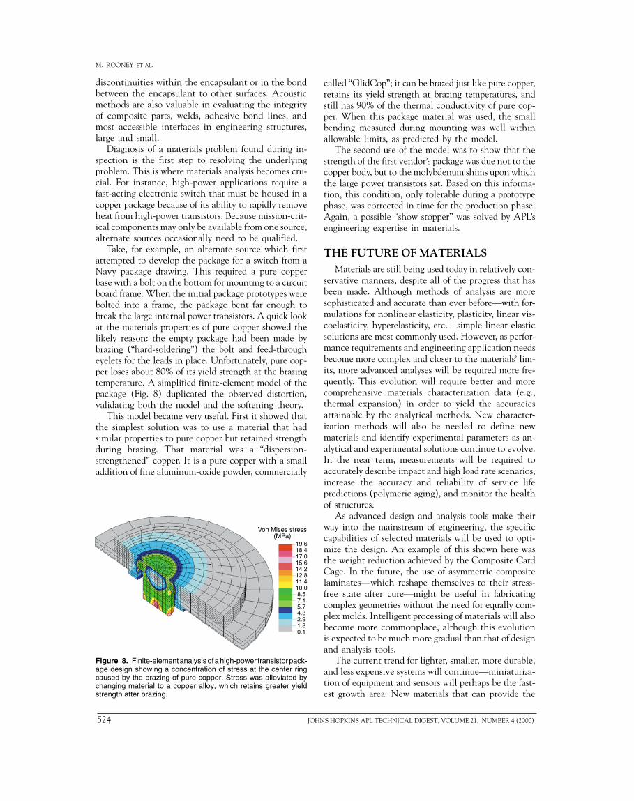
Diagnosis of a materials problem found during in-spection is the first step to resolving the underlyingproblem. This is where materials analysis becomes cru-cial. For instance, high-power applications require afast-acting electronic switch that must be housed in acopper package because of its ability to rapidly removeheat from high-power transistors. Because mission-crit-ical components may only be available from one source,alternate sources occasionally need to be qualified.
Take, for example, an alternate source which firstattempted to develop the package for a switch from aNavy package drawing. This required a pure copperbase with a bolt on the bottom for mounting to a circuitboard frame. When the initial package prototypes werebolted into a frame, the package bent far enough tobreak the large internal power transistors. A quick lookat the materials properties of pure copper showed thelikely reason: the empty package had been made bybrazing (“hard-soldering”) the bolt and feed-througheyelets for the leads in place. Unfortunately, pure cop-per loses about 80% of its yield strength at the brazingtemperature. A simplified finite-element model of thepackage (Fig. 8) duplicated the observed distortion,validating both the model and the softening theory.
This model became very useful. First it showed thatthe simplest solution was to use a material that hadsimilar properties to pure copper but retained strengthduring brazing. That material was a “dispersion-strengthened” copper. It is a pure copper with a smalladdition of fine aluminum-oxide powder, commercially
Figure 8. Finite-element analysis of a high-power transistor pack-age design showing a concentration of stress at the center ringcaused by the brazing of pure copper. Stress was alleviated bychanging material to a copper alloy, which retains greater yieldstrength after brazing.
called “GlidCop”; it can be brazed just like pure copper,retains its yield strength at brazing temperatures, andstill has 90% of the thermal conductivity of pure cop-per. When this package material was used, the smallbending measured during mounting was well withinallowable limits, as predicted by the model.
The second use of the model was to show that thestrength of the first vendor’s package was due not to thecopper body, but to the molybdenum shims upon whichthe large power transistors sat. Based on this informa-tion, this condition, only tolerable during a prototypephase, was corrected in time for the production phase.Again, a possible “show stopper” was solved by APL’sengineering expertise in materials.
THE FUTURE OF MATERIALSMaterials are still being used today in relatively con-
servative manners, despite all of the progress that hasbeen made. Although methods of analysis are moresophisticated and accurate than ever before—with for-mulations for nonlinear elasticity, plasticity, linear vis-coelasticity, hyperelasticity, etc.—simple linear elasticsolutions are most commonly used. However, as perfor-mance requirements and engineering application needsbecome more complex and closer to the materials’ lim-its, more advanced analyses will be required more fre-quently. This evolution will require better and morecomprehensive materials characterization data (e.g.,thermal expansion) in order to yield the accuraciesattainable by the analytical methods. New character-ization methods will also be needed to define newmaterials and identify experimental parameters as an-alytical and experimental solutions continue to evolve.In the near term, measurements will be required toaccurately describe impact and high load rate scenarios,increase the accuracy and reliability of service lifepredictions (polymeric aging), and monitor the healthof structures.
As advanced design and analysis tools make theirway into the mainstream of engineering, the specificcapabilities of selected materials will be used to opti-mize the design. An example of this shown here wasthe weight reduction achieved by the Composite CardCage. In the future, the use of asymmetric compositelaminates—which reshape themselves to their stress-free state after cure—might be useful in fabricatingcomplex geometries without the need for equally com-plex molds. Intelligent processing of materials will alsobecome more commonplace, although this evolutionis expected to be much more gradual than that of designand analysis tools.
The current trend for lighter, smaller, more durable,and less expensive systems will continue—miniaturiza-tion of equipment and sensors will perhaps be the fast-est growth area. New materials that can provide the
Von Mises stress(MPa)
19.618.417.015.614.212.811.410.08.57.15.74.32.91.80.1

JOHNS HOPKINS APL TECHNICAL DIGEST, VOLUME 21, NUMBER 4 (2000) 525
ADVANCED MATERIALS: CHALLENGES AND OPPORTUNITIES
same function in less space, much like transistors re-placed vacuum tubes, will be needed to accomplish this.New processes for integrating existing materials on asmaller size scale will also likely be needed. Methodsof joining dissimilar materials, and doing so reliably ina lasting fashion, will become a critical enabling tech-nology. MEMS devices will become more and moreprevalent as applications are found that can take ad-vantage of their capabilities. This is already beginningto happen in the field of biomedical devices. Intelligentprocessing and service life determinations will profitfrom miniaturized and integrated sensors (embedded),and it is expected that monitoring of structural healthwill become a reality for buildings, aircraft, and bridges.Sensor technologies are already becoming small enoughand cheap enough (temperature, pressure, and humid-ity sensors are readily available in microchip form) foruse in automobiles and personal computers.
As smaller and more multilayer structures are de-signed and fabricated, however, they will present in-creasing difficulties for those who must characterize andinspect them. The methods used to inspect tomorrow’sproducts will need to improve both in resolution andsensitivity. As we learn to understand the limits of thesemethods, it is expected that the materials and systemsof the future will begin to incorporate elements thatwill recognize when they begin to fail and either notifythe user of expended shelf life or initiate self-healing.Many of the smart materials concepts that are beingproposed today point toward self-diagnostic and auto-mated response systems. While known to many of usonly in toy form, mechanisms that “transform” fromone function or form to another will find their way intoengineering applications. Space exploration alreadyrequires many components to function on multiplelevels. Thus, components that can adapt and evolve forsuccessive missions or in response to changes in envi-ronment will be needed.
SUMMARYOur ability to solve the engineering challenges of
today and tomorrow is still being driven by cost andavailability. Materials and processing methods thatyield equivalent or improved performance at lower cost,such as the SCRIMP®, rapid prototyping, and othertechnologies referred to in this article, are being active-ly pursued. Additional streamlining and optimization ofthe design process will be needed to further reduce thecost of implementing new materials, to have confi-dence in their ability to perform as intended, and totake full advantage of their properties. Our understand-ing of how materials interact, how they can be reliablyjoined or integrated, which ones to select or avoid forspecific applications or environments, and even how tochange or tailor their properties is expanding daily.
The challenges, as well as the opportunities, willbe in all areas of materials development: synthesis,fabrication, integration, characterization, and inspec-tion. Sensor development will continue to requirenew, targeted materials. Fabrication methods will bedriven to less costly and faster processes. Next-gener-ation (“smart”) materials will need to continue tofunction over time when joined or even intimatelyintegrated with other components. New and especiallyexisting materials will need to be characterized inmore depth and with greater accuracy so that theirperformance can be pushed to the limits more reliably.Finally, designed and integrated materials will mostlikely present more difficulties in verifying their integ-rity and reliability by conventional means than everbefore. TSD will continue to support APL’s missionareas by maintaining and expanding its capabilities tokeep pace with advances in materials and associatedtechnologies.
REFERENCES1Accelerated Insertion of Materials (AIM), Broad Agency Announcement BAA
00-22, Defense Advanced Research Projects Agency, Washington, DC,available at http://www.darpa.mil/baa00-22/dso (accessed 10 Apr 2000).
2National Defense Budget Estimates for FY 2000, available on the DoD Web siteat http://www.dtic.mil/comptroller/fy2000budget/GREEN2000.pdf (accessed11 Apr 2000).
3Aging of U.S. Air Force Aircraft, National Materials Advisory Board FinalReport, NMAB-488-2, National Academy Press, Washington, DC (1997).
4Air Force Dual Use Science & Technology (AF DUS&T) Program, AFRL-sponsored Web site, available at http://www.afrl.af.mil/dualuse/index.htm(accessed 11 Apr 2000).
5Acquisition Reform Change Elements, Department of the Navy Web site,available at http://www.acq-ref.navy.mil/implmanc.html (accessed 10 Apr2000).
6APL Space Department Web site, available at http://www.timed.jhuapl.edu/mission/missiondescription.htm (accessed 10 Apr 2000).
7APL Space Department Web site, http://sd-www.jhuapl.edu/MESSENGER/(accessed 10 Apr 2000).
8Charles, H. K., Jr., “Materials in Electronics Packaging at APL,” Johns HopkinsAPL Tech. Dig. 14(1), 51–67 (1993).
9Charles, H. K., Jr., “APL’s Packaging Future: The Next Few Years,” JohnsHopkins APL Tech. Dig. 20(1), 101–110 (1999).
10Arnold, B. A., Euler, A. C., Jenkins, A. L., Uy, O. M., and Murray, G. M.,“Progress in the Development of Molecularly Imprinted Polymer Sensors,”Johns Hopkins APL Tech. Dig. 20(2), 190–198 (1999).
11Jenkins, A. L., Uy, O. M., and Murray, G. M., “Polymer Based LanthanideLuminescent Sensor for the Detection of the Hydrolysis Product of the NerveAgent Soman in Water,” Anal. Chem. 71, 373–378 (1999).
12Murray, G. M., Site Selective Ion Exchange Resins Templated for Lead (II) Ionand Methods and Devices for Their Use, U.S. Patent # 5,814,671 (29 Sep 1998).
13Bae, S. Y., Zeng, X., and Murray, G. M., “A Photometric Method for theDetermination of Pb2+ Following Separation and Preconcentration Using aTemplated Ion Exchange Resin,” J. Anal. At. Spectrosc. 10, 1177–1181(1998).
14Bae, S. Y., Southard, G. L., and Murray, G. M., “Molecularly Imprinted IonExchange Resin for Purification, Preconcentration and Determination ofUO2
2+ by Spectrophotometry and Plasma Spectrometry,” Anal. Chim. Acta397, 173–181 (1999).
15Bevan, M. G., and Romenesko, B. M., “Modern Electronic PackagingTechnology,” Johns Hopkins APL Tech. Dig. 20(1), 22–33 (1999).
16Oursler, D. A., Wickenden, D. K., Zanetti, L. J., Kistenmacher, T. J., Givens,R. B., et al., “Development of the Johns Hopkins Xylophone Bar Magnetom-eter,” Johns Hopkins APL Tech. Dig. 20(2), 181–189 (1999).
17Schaefer, E., Tomkiewicz, R. L., and Wienhold, P. D., “Development of aLow-Cost Composite Optical Bench for Space Application,” in Proc. 6th Ann.Int. Conf. on Comp. Eng. (Orlando, FL), pp. 729–730 (Jun 1999).
18Dawson, D. K., “Inside Manufacturing: SCRIMPing Saves Money and Time,”Compos. Technol. 5(5), 21 (Sep/Oct 1999).
19Wienhold, P. D., and Wozniak, J. J., “The Application of SCRIMP VARTMFabrication Technology to the Compressed Natural Gas Integrated StorageSystem,” 29th SAMPE J. 34(1), 5–10 (Jan/Feb 1998).

M. ROONEY ET AL.
526 JOHNS HOPKINS APL TECHNICAL DIGEST, VOLUME 21, NUMBER 4 (2000)
20Krantz, D. G., Belk, J. H., and Biermann, P. J., “Early Demonstrations ofRemotely Queried Microsensors,” SPIE 3673, 190–194 (Mar 1999).
21DuBow, J., Zhang, W., Lu, Y., Bingham, J., Syammach, F., et al., “EmbeddedCure Monitor and Strain Gauge,” SPIE 3673, 336–350 (Mar 1999).
22Midcourse Space Experiment, Contamination Experiment Data AnalysisCenter Web site, available at http://www.jhuapl.edu/cedac/ (accessed 11 Apr2000).
23Wood, B. E., Hall, D. F., Lesho, J. C., Uy, O. M., Boies, M. T., et al., “QCMFlight Measurements of Contaminant Films and Their Effect on MidcourseSpace Experiment (MSX) Satellite Optics,” SPIE 3124, 34–40 (1997).
24Uy, O. M., Cain, R. P., Carkhuff, B. G., Cusick, R. T., and Wood, B. E.,“Miniature Quartz Crystal Microbalance for Spacecraft and Missile Applica-tions,” Johns Hopkins APL Tech. Dig. 20(2), 199–213 (1999).
25Jackson, J. J., “Modeling of a Bio-Resorbable Composite Material for DesignOptimization of Internal Fixation Devices,” in Proc. 1999 Summer Bioengineer-ing Conf., ASME 42, 187–188 (Jun 1999).
26Atalar, E., Bottomley, P. A., and Zerhouni, E. A., “High ResolutionIntravascular MRI and MRS by Using a Catheter Receiver Coil,” Magn.Reson. Med. 36(4), 596–605 (1996).
27Simon, M., Athanasoulis, C. A., and Kim, D., “Simon Nitinol Inferior VenaCava Filter: Initial Clinical Experience,” Radiol. 172, 99–103 (1989).
28Wienhold, P. D., Mehoke, D. S., Roberts, J. C., and Schaefer, E. D., “TheDesign and Fabrication of a Low Cost Spacecraft Card Cage,” in Proc. 42ndSAMPE ISSE Conf. 42, pp. 802–812 (May 1997).
29Mehoke, D. S., Feldmesser, H. S., and Grimm, P. D., “System-LevelPackaging: Putting It All Together,” Johns Hopkins APL Tech. Dig. 20(1),81–90 (1999).
30Roberts, J. C., Luesse, M. H., and Magee, T. C., “A Technique for LocallyIncreasing Surface Heat Spreading and the Through-Thickness Thermal
Conductivity of Graphite Fiber/Epoxy Laminates,” J. Comp. Mater. 30(2),231–247 (1006).
31Roberts, J. C., and Carkhuff, B. G., “Transient and Steady-State Temperaturesin Hybrid High/Low Thermal Conductivity Composites,” in Proc. Am. Soc.Composites, 10th Tech. Conf. on Composite Materials, pp. 512–522 (Oct 1995).
32Carkhuff, B. G., and Roberts, J. C., “A Test Fixture for Mapping ThermalConduction in Composites Under Transient and Steady-State Conditions,”Exp. Tech. 21, 12–14 (May/June 1997).
33Bailey, L. E., Roberts, J. C., and Jones, D., “Optimal Design Parametersfor Thermal and Mechanical Performance of a Metal/Composite Joint,”J. Thermopl. Comp. Mater. 10, 362–380 (Jul 1997).
34Roberts, J. C., “Analytic Techniques for Sizing the Walls of AdvancedComposite Electronics Enclosures,” J. Comp. Eng. Part B 30(2), 177–187(Mar 1999).
35Roberts, J. C., and Wienhold, P. D., “The Design, Analysis and Fabricationof a Composite Electronics Enclosure Flanged Aperture with Supporting EMITest Data,” J. Comp. Mater. 29(14), 1834–1849 (1995).
36Wienhold, P. D., Mehoke, D. S., Roberts, J. C., Seylar, G. R., and Kirkbride,D. L., “Electromagnetic Interference (EMI) Shielding Effectiveness,Surface Resistivity, and RF Conductivity of Thin Composites for SpacecraftApplications,” in Proc. 30th Int. SAMPE Tech. Conf. 30, pp. 243–255(20–24 Oct 1998).
37Thermal Endurance of Materials from TGA Decomposition Data, ASTM StandardE1877-97, American Society for Testing and Materials, 14.02 (1997).
38Seferis, J. C., “Aging Analyses of Polymer Composites Through Time-Temperature Equivalence,” J. Comp. Tech. Res. 21(3), 173–179 (Jul 1999).
39Moor, A. F., Casasnovas, A., and Purwin, S. R., “The Case for Plastic-Encapsulated Microcircuits in Spaceflight Applications,” Johns Hopkins APLTech. Dig. 20(1), 91–100 (1999).
THE AUTHORS
MICHAEL ROONEY is a Senior Professional Staff Engineer in APL’s TechnicalServices Department. He holds a B.S. in engineering science and mechanicsfrom Virginia Tech and M.S.E. and Ph.D. degrees in materials scienceand engineering from The Johns Hopkins University. Dr. Rooney is theSupervisor of the Materials Application and Development Section of TSD.He specializes in the characterization, process control, and nondestructiveevaluation of materials for advanced engineering applications. He is a memberof the American Society for Nondestructive Testing and the Society for theAdvancement of Materials and Process Engineering. His e-mail address [email protected].
JACK C. ROBERTS is a Principal Professional Staff Engineer in APL’sTechnical Services Department as well as a Research Professor and AdjunctProfessor in the Department of Mechanical Engineering at The Johns HopkinsUniversity. He holds B.S. and M.S. degrees in mechanical engineering fromthe University of Michigan and a Ph.D. from Rensselaer Polytechnic Institute.His work has centered on structural analysis, design, biomechanics, orthopedicimplant design, fracture, tribology, and crash worthiness with materials as diverseas structural steel, continuous fiber composites, and bone. Dr. Roberts has 4patents and over 70 technical publications in his field. His e-mail address [email protected].
JOHNS HOPKINS APL TECHNICAL DIGEST, VOLUME 21, NUMBER 4 (2000) 527
ADVANCED MATERIALS: CHALLENGES AND OPPORTUNITIES
GEORGE M. MURRAY is a Senior Professional Staff Chemist in APL’sTechnical Services Department. He received a B.A. in chemistry in 1982 and aPh.D. in chemistry in 1988, both from the University of Tennessee, Knoxville.He performed his postdoctoral research at the Transuranium Research Laboratoryof Oak Ridge National Laboratory. Dr. Murray’s research interests focus ondeveloping methods of analysis for the ultratrace determination of toxicsubstances in real samples. His laboratory specializes in the production ofimprinted polymers and spectrochemical analysis. He is a member of theAmerican Chemical Society and the Society for Applied Spectroscopy. Dr.Murray’s e-mail address is [email protected].
BRUCE M. ROMENESKO is a Principal Professional Staff Physicist in APL’sTechnical Services Department. He holds a B.S. in mathematics and physicsfrom the University of Wisconsin and a Ph.D. in experimental solid-state physicsfrom the University of Maryland. Dr. Romenesko is responsible for the packagingand failure analysis of high-reliability electronics, including hybrid microcircuits,solder/surface mounted devices, and board-level assemblies. He has also beenactive in experimentation in microwave hybrid circuit reliability, radiationtesting of electronics used in spacecraft programs, and ball grid array packagingtechnologies. Dr. Romenesko has published over 40 papers in his field. He iscurrently a member of the IEE and IMAPS, and serves IMAPS as its Mid-Atlantic Regional Director and Chair of the Interconnections Subcommittee.His e-mail address is [email protected].