advanced computing - federation of american scientists · pdf filetera computer advanced...
TRANSCRIPT
ADVANCED COMPUTING
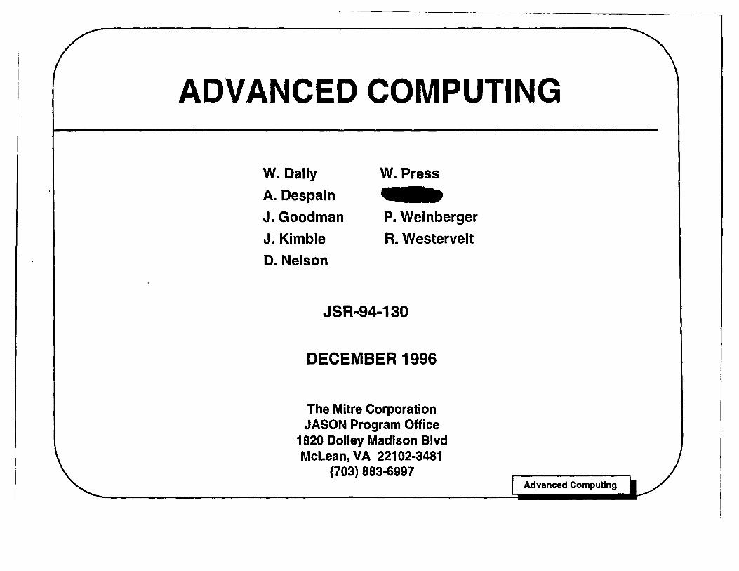
w. Dally
A. Despain
J. Goodman
J. Kimble
D. Nelson
W. Press
~ P. Weinberger
R. Westervelt
JSR-94-130
DECEMBER 1996
The Mitre Corporation JASON Program Office
1820 Dolley Madison Blvd McLean, VA 22102-3481
(703) 883-6997 Advanced Computing

REPORT DOCUMENTATION PAGE Fann AppfDV«I OMS No. 0704..0'.
PublIc qpotIlng IIunIMI tor UIia coIlectloll 01 Infonnation ........... to -..g. 1 hour per r • ..,o .... Including "'. IiIM !Dr review InsIndID ..... ere hInII .JdMIng d ... eau_ ........ MIl IIIIInIMIIng ... d ... IIHIIed, ... compIeIlno MIl ...... , ... coIIKIion 0I1n10fJM11011. Send co ......... reoenIlno I .... lIUftIen ......... ar 1lIIY allier MptICt 01 ... IIIIIIecIIaII at IdoIInMIaII, IndIIdlnll qglllloIIa far reducing "' .. burden, ID Wuhlnglan HHClqullrleIS SIIVIcM, DIrKtO,... far 1nI_llan 0pera1lonS ... RejICIIIII. 121& M_ o. .. Hili...,. S ..... 121M. Arlington. VA 22202-43112, MIl to ... OIIice of ......... nl and Budpl. P~k RedUCIlDn ProjeCt (0704-0188). Waehlngtan. DC 20&03-
1. AGENCY use ONLY (lAv. blank) 12. REPORT DATE r' REPORT TYPE AND DATES COVERED December 1996
'" nTLE AND SUBnTLE s. RJNDlNG NUMBERS
Advanced Computing
" AUlHOR(S) 13-958534-04
~ A Despain, J. Goodman, J. Kimble, D. Nelson, W. Press, P. Weinberger, R Westervelt
7. PERFORMING ORGANIZAnON NAME($) AND ADDRESS(ES) a. PERFORMING ORGANlZA1l0N
The MITRE Corporation REPORT NUMBER
JASON Program Office JSR-94-130 1820 Dolley Madison Blvd
McLean, Virginia 22102
t. SPONSORINGIMONITORING AGENCY NAME(S) AND ADDRESS(ES) 10. SPONSORlNGlMONITORING AGENCY REPORT NUMBER
Advanced Research Projects Agency 3701 North Fairfax Drive JSR-94-130 Arlington, Va. 22203-1714
11. SUPPLEMENTARY NOTES
12a. DISTRIBUnONIAVAILABIUTY STATEMENT 12b. DlSTRlBUllON CODE
Approved for public release; distribution unlimited. Distribution Statement A
~3. ABSTRACT (MuJmum 200 -rrlsJ
The task of the study was to examine technical issues associated with the design and construction of advanced computers ona twenty year time frame.
Focus was on two topiCS: superconducting and "single electron" logic, and advanced . architecture.
~4. SUBJECT TERMS
single electron, advanced architecture
7. SECURITY CLASSIFICAnoN 18. SECURITY CLASSIFICAnON OFAEPORT OF THIS PAGE
Unclassified Unclassified _7U04t_ 19. SECURITY CLASSIFICATION
OF ABSTRACT
Unclassified
115. NUMtsl:tt OF PAGES
11ti. PHI,-"I:: ,-"UUI::
110. ur ..............
SAR
Stand.,., Farm 211 lAw. 2-11, -.,---, . • "·'02

Table of Contents
Section Page
Introduction 1
Superconducting and Single Electronics 13
Conclusions: Superconducting and Single Electronics 47
Advanced Architecture 51
Conclusions: Advanced Architecture 94
Advanced computing, iii
This page left blank intentionally
Advanced computing,
----------------- .. ~- ~- --

Introduction
Advanced computing, 1

Introduction
This briefing was presented by Bob Westervelt and Bill Dally; other JASONs who contributed to the project are listed.
The task of the study was to examine technical issues associated with the design and construction of advanced computers on a twenty year time frame. Current CMOS technology was not covered, because it has been examined in detail by other groups and its future development can be predicted reasonably well.
We focused on two topics: superconducting and "single electron" logic, and advanced architecture. The first half of this brief, presented by Bob Westervelt, describes single flux quantum and single electron logic; the second half, presented by Bill Dally, discusses architecture issues.
Advanced Computing .. ~ ______ •• 2
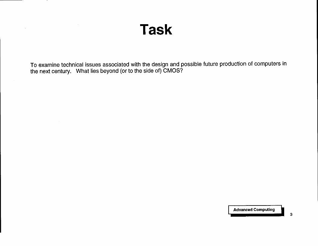
Task
To examine technical issues associated with the design and possible future production of computers in the next century. What lies beyond (or to the side of) CMOS?
Advanced Computing .. ~ ______ •• 3
---------------------------------~--------
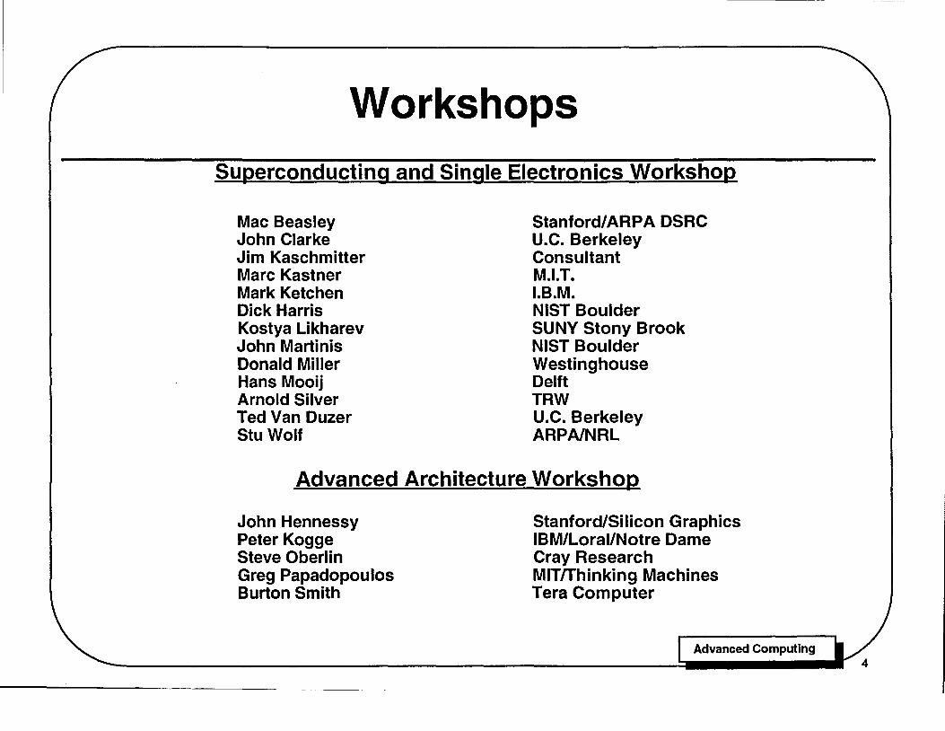
Workshops Superconducting and Single Electronics Workshop
Mac Beasley John Clarke Jim Kaschmitter Marc Kastner Mark Ketchen Dick Harris Kostya Likharev John Martinis Donald Miller Hans Mooij Arnold Silver Ted Van Duzer Stu Wolf
Stanford/ARPA DSRC U.C. Berkeley Consultant M.I.T. I.B.M. NIST Boulder SUNY Stony Brook NIST Boulder Westinghouse Delft TRW U.C. Berkeley ARPAlNRL
Advanced Architecture Workshop
John Hennessy Peter Kogge Steve Oberlin Greg Papadopoulos Burton Smith
Stanford/Silicon Graphics IBM/Loral/Notre Dame Cray Research MITlThinking Machines Tera Computer
Advanced Computing
Workshops
Two workshops were held during the summer study in La Jolla, one on superconducting and single electronics, and one on advanced architecture. A number of distinguished researchers from academia and industry, listed above, either attended the workshops, or were consulted separately.
Advanced Computing .. '"w ______ .. 1 5
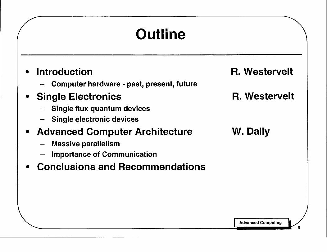
Outline
• Introduction - Computer hardware - past, present, future
• Single Electronics - Single flux quantum devices - Single electronic devices
• Adva·nced Computer Architecture - Massive parallelism - Importance of Communication
• Conclusions and Recommendations
R. Westervelt
R. Westervelt
W. Dally
Advanced Computing
-- --~------- --- ----
Outline
The briefing consisted of three parts, an introduction to general issues concerning computer hardware in the past, present, and future, presented by Bob Westervelt, a description of two possible future technologies - single flux quantum logiC and single electron logic - by Bob Westervelt, and a discussion of advanced computer architecture, presented by Bill Dally and written up separately.
Advanced Computing .. ~ ______ •• 7

SIA Roadmap for CMOS Technology
Year 1995 1998 2001 2004 2007
Feature size (microns) 0.35 0.25 0.1S 0.12 0.1 Gates/chip SOOk 2M 5M 10M 20M Bits/chip DRAM 64M 265M 1G 4G 16G Bits/chip SRAM 16M 64M 256M 1G 4G Chip size (mm2) Logic/microprocessor 400 600 SOO 1000 1250 Chip size (mm2) DRAM 200 320 500 700 1000 Wafer diameter (mm) 200 200-400 200-400 200-400 200-400 Interconnect levels (logic) 4-5 5 5-6 6 6-7 Max power (W/die) High Performance 15 30 40 40-120 40-200 Power supply (V) (Portable) 2.2 2.2 1.5 1.5 1.5 Number of I/Os 750 1500 2000 3500 5000 Performance (MHz) Off-chip 100 175 250 350 500 Performance (MHz) On-chip 200 350 500 700 1000
Advanced Computing

SIA Road Map for CMOS Technology
Representatives from the Semiconductor Industry Association (SIA) have met to consider the future of CMOS technology. This table summarizes their predictions up to the year 2007. These predictions are considered to be reasonably conservative, and the consensus is that the predicted level of performance will probably be achieved.
We use this chart to illustrate a number of points, dealt with in detail later by Bill Dally:
• Driven primarily by the reduction of feature size, the number of gates per chip will increase dramatically by 2007; for example, the DRAM size will increase by a factor of one thousand to 16 Gbits per Chip. The predicted increase in clock speed is much smaller, only a factor of five to 1 GHz, on Chip.
• The explosion in memory size combined with a moderate increase in clock speed mean that massive parallelism will be required to utilize the memory and obtain a large increase in computational power. Mas'sive parallelism presents challenges both for computer architecture (particularly communication) and for parallel software (efficient use of many processors).
• The chip area devoted to each processor will shrink with the reduction in feature size, so that memory will consume most of the available chip area. This is already true today, but processors and memory are located on separate chips made on separate fabrication lines, and processors are priced much higher. In the future, processors and memory are likely to be found on the same chip made in the same line in order to take advantage of high speed communication on chip. Memory will dominate the chip area and cost, while processors will be relatively inexpensive.
Advanced Computing '-~ ______ ... 9
Performance and Predictions in the 1970's
• Microprocessors in their infancy
• Cray 1 supercomputer (late 1970's) - ECl bipolar logic circuits - 100k chips x 4 gates/chip = 400k gates - 256 MByte SRAM memory (maximum)
- .so MHz clock speed
• Mainstream predictions for the 1990's - (all incorrect) - High end computers will use bipolar logic. - Mainframes will dominate micro's.
- CMOS logic is special purpose only - low power, slow.
- 1 Jlm linewidth is a fundamental limit.
• Caution is advised! - Support a range of alternative technologies.
Advanced Computing

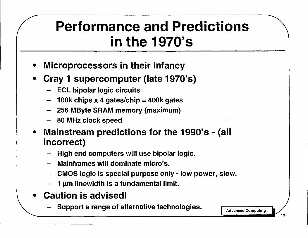
Performance and Predictions in the 1970's
When attempting to predict what will happen twenty years in the future, it is useful to look twenty years in the past.
In the 1970's microprocessors were in their infancy, and microprocessor based computers had very limited capabilities.
The Cray 1 supercomputer, marketed in the late 1970's, used emitter coupled logic (ECl) and bipolar transistor technology, had about 100,000 chips with about 4 gates per chip, could address a maximum of 256 MBytes of SRAM memory, and ran at a clock speed of 80 MHz. This level of performance has now been surpassed by microprocessor-based systems.
Many mainstream predictions made twenty years ago for computers in the 1990's turned out to be incorrect.. What seemed like conservative good sense then, looks less good now. For example:
• High end computers will use bipolar transistors, because they are faster than FET's. The importance of heat production in densely packed integrated circuits was underestimated.
• Mainframes will dominate microcomputers. It was felt that the dominant market would be large business and government users, and that the value of the installed software base would provide the inertia to keep mainframes on top.
• CMOS logic is special purpose only - low power and slow. CMOS was slow with 5 Jlm design rules used in the 1970's, and required special operating voltages. The importance of compactness and low power as fundamental attributes were under appreciated, as well as the speed which could be attained.
Advanced Computing '-,. ............ ~'11

Performance and Predictions in the 1970's (concluded)
• One micron feature size is a fundamental limit. This sounds reasonable given the 0.5 J.lm wavelength of light, but has not held up. Nonlinear resists and advanced processing permit 0.5 J.lm features now, and 0.1 J.lm features are predicted in the year 2007 according to the SIA roadmap.
Caution is advised! Twenty years is a long time over which to predict the future, particularly in a field as active as computers. It is clear that CMOS technology will continue to be important and viable in the future, and will attract major industrial investment. However, it is less clear that CMOS will still be dominant twenty years from now, particularly given the high projected cost of fabrication lines. Revolutions in performance are likely to come through new advances in processing, driven in part by these high costs.
Given the uncertainties, a sensible approach is to invest in a range of exploratory research.
Advanced Computing .. ~ ______ •• 12
I Advanced Computing L. ,.. ____ .... ·13

Single Electronics
Single Flux Quantum Logic
Single Flux Quantum Logic
Magnetic-': Circulating Flux Line Supercurrent I
Superconducting Loop
I of Cooper Pairs ......--.
Magnetic Flux 51 through Loop h Flux Quantum
n«l»o = -2 (Cooper Pairs) «I» = n«l»o + const. e
..,... -+ --+ J(hk - 2eA) • ds = nh + const.
loop
Single Electron Logic
Single Electron Logic
Single Electron '" LTunnel
~ Junctions
>-@-t: / " Isolated Metal
Metal Tunnel Island Contacts
Quantization of Charge
~
Advanced Computing
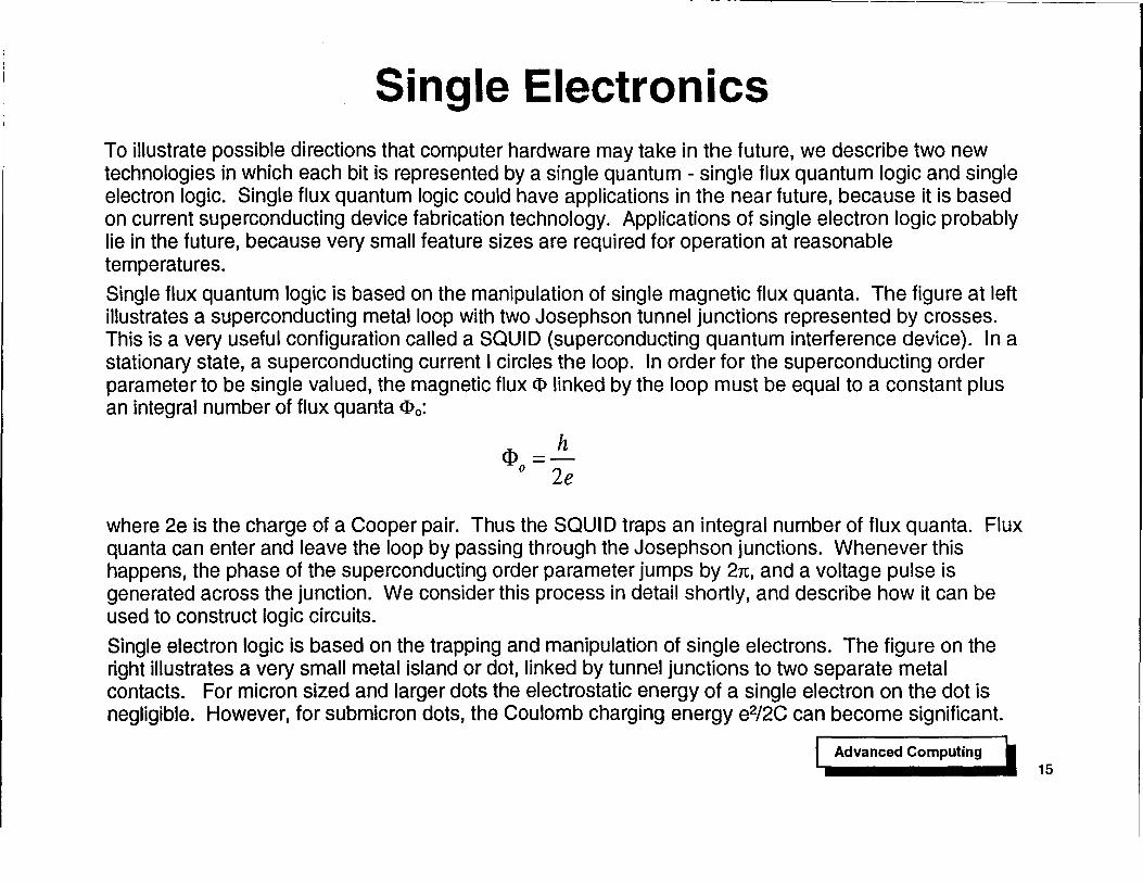
Single Electronics To illustrate possible directions that computer hardware may take in the future, we describe two new technologies in which each bit is represented by a single quantum - single flux quantum logic and single electron logic. Single flux quantum logic could have applications in the near future, because it is based on current superconducting device fabrication technology. Applications of single electron logic probably lie in the future, because very small feature sizes are required for operation at reasonable temperatu res.
Single flux quantum logic is based on the manipulation of single magnetic flux quanta. The figure at left illustrates a superconducting metal loop with two Josephson tunnel junctions represented by crosses. This is a very useful configuration called a SQUID (superconducting quantum interference device). In a stationary state, a superconducting current I circles the loop. In order for the superconducting order parameter to be single valued, the magnetic flux <I> linked by the loop must be equal to a constant plus an integral number of flux quanta <1>0:
cI>=~ o 2e
where 2e is the charge of a Cooper pair. Thus the SQUID traps an integral number of flux quanta. Flux quanta can enter and leave the loop by passing through the Josephson junctions. Whenever this happens, the phase of the superconducting order parameter jumps by 21t, and a voltage pulse is generated across the junction. We consider this process in detail shortly, and describe how it can be used to construct logiC circuits.
Single electron logic is based on the trapping and manipulation of single electrons. The figure on the right illustrates a very small metal island or dot, linked by tunnel junctions to two separate metal contacts. For micron sized and larger dots the electrostatic energy of a single electron on the dot is negligible. However, for submicron dots, the Coulomb charging energy e2/2C can become significant.
Advanced Computing L. ~ ______ .. ' 15

Single Electronics (concluded)
If e2/2C is larger than the thermal energy kT, and the tunneling resistance of each contact is greater than h/e2, the number of electrons on the dot becomes well-defined, and the quantization of electronic charge leads to the requirement that the total charge Q on the dot be an integral multiple of e. Electrons pass onto and off of the dot by tunneling to one of the metal contacts, generating a current pulse. We describe below how these physical processes can be used to construct memory elements.
In the following presentation, we treat single flux quantum logic first, then describe single electron logic.
Advanced Computing .. ~ ______ .. ' 16

This page intentionally left blank.
Advanced Computing 17
eq. of Motion
RCSJ Model
OJ,cur+ent I
" C R Voltage V JJ ~
Critical Current Ic
I = c~y +~V + Icsine
~~ =2~V e is the phase of the superconducting order parameter
eq. of Motion of Mass m in tilted sin x Potential
( C-I1)d2e (-11) de d 2e dt2 = - 2eR dt - de (lccose - Ie)
washboarf Potential
U~) 1aW
d2x de d m dt2 =-"1 dt - dx U(x)
CurrentVoltage
Characteristic
V
Phase e de L-_-.!'~_+ __ ~_, Vadf
Ic Critical
o e
Advanced Computing
RCSJ Model
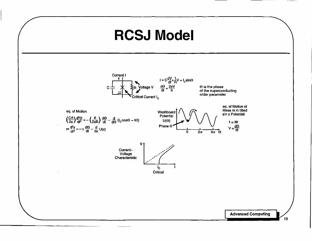
In order to understand the operation of single flux quantum logic, we need first to understand Josephson junctions. The RCSJ (resistively and capacitively shunted junction) model of Josephson junctions represents an actual device by a parallel combination of an ideal junction with a capacitance C and resistance R. This model describes the operation of experimental devices very well. The equations of motion for the RCSJ model are given to the right of its circuit diagram: the total current I is the sum of capacitive and resistive contributions with the Josephson current Ie sin 9, where Ie is the critical current of the junction beyond which it develops voltage, and 9 is the difference of the phase of the superconducting order parameter across the junction. The voltage Vis given by the second Josephson equation V=(h/2e)d9/dt. These two first order differential eq'uations can be combined into one second-order differential equation for the phase difference 9(t), as shown.
It is an interesting and very useful fact that the equation of motion for the phase 9(t) in the RCSJ model is exactly the same as the equation of motion for the position x(t) of a ball of mass m moving in a tilted sinusoidal washboard potential U with viscous damping y. As shown, the mass m is proportional to C, and the damping y is proportional to 1/R. The tilt of the washboard potential is proportional to the current I in the RCSJ model, and the velocity is proportional to the voltage V
Using the tilted washboard representation, we can understand the origin of the measured current voltage characteristics of actual Josephson junctions. The overdamped case (small R) is most relevant to the present discussion. Suppose that the slope of the washboard potential is initially small, and the ball is at rest in one of the potential minima as shown. As indicated on the schematic current voltage characteristic, this situation applies to currents I < 'e, for which the voltage is zero. The ball is trapped until the slope added to the washboard potential destroys the local minimum, and the ball starts rolling.
Advanced Computing ~ ,. .............. ' 19
RCSJ Model (concluded)
As indicated this occurs above I = Ie, for which the voltage V > O. For the overdamped case the ball loses enough energy through each cycle of the potential that it is retrapped immediately if the applied slope falls below the critical value. Thus the voltage V across an overdamped junction rapidly switches on and off as the applied current passes above or below Ie, and the maximum switching rate is 11 t - IJ2e both on and off. At low temperatures one can show that the maximum switching rate for overdamped junctions is essentially limited by the ~uperconducting energy gap .1, corresponding to THz frequencies for practical superconductors. Overdamped junctions have the additional virtue that they are relatively simple and robust, and can be fabricated by a wide range of techniques.
Underdamped junctions used in many previous families of superconducting logic circuits have hysteretiC current voltage characteristics, and more complex behavior. For the underdamped case, the ball representing the phase does not lose enough energy in one cycle of the periodic washboard potential to be retrapped. Thus the motion representing voltage can continue even if the slope is reduced somewhat below the critical value, resulting in a hysteretic current-voltage characteristic. This hysteresiS is a useful type of switching behavior, but hysteretiC junctions suffer the serious disadvantage that the retrapping time is typically many times longer than the detrapping time. Fast logic using hysteretiC junctions requires an ac supply which forcibly turns the junctions off.
Advanced Computing .. a...-______ .. I 20

This page intentionally left blank.
Advanced Computing L. ,. ______ .. 121

Rapid Single Flux Quantum (RSFQ) Logic
SQUID ® Josephson junctions
V2 V 0 2p phase slip flux
.JIIC:'---~ quantum escape trapped flux quantum ~ supercurrent I
(V 1 = V 2 = 0) Ib Ib Ib Ib
Josephson Transmission Line
RS Flip Flop
+ + + +
~ If lel < Fo Flux Quantum Transmitted --.
S
set reset pulse pulse
Advanced Computing
Rapid Single Flux Quantum (RSFQ) Logic
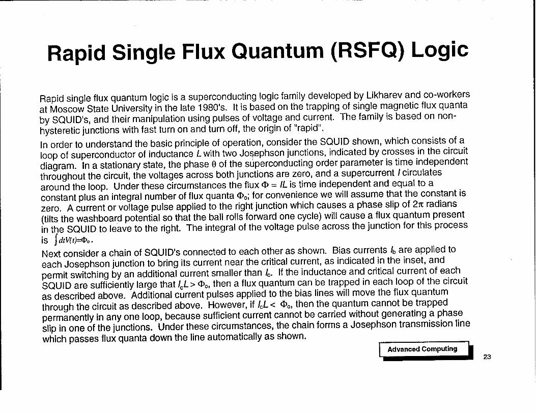
Rapid single flux quantum logic is a superconducting logic family developed by Ukharev and co-workers at Moscow State University in the late 1980's. It is based on the trapping of single magnetic flux quanta by SQUID's, and their manipulation using pulses of voltage and current. The family is based on nonhysteretic junctions with fast turn on and turn off, the origin of "rapid".
In order to understand the basic principle of operation, consider the SQUID shown, which consists of a loop of superconductor of inductance L with two Jo~,ephson junctions, indicated by crosses in the circuit diagram. In a stationary state, the phase e of the superconducting order parameter is time independent throughout the circuit, the voltages across both junctions are zero, and a supercurrent I circulates around the loop. Under these circumstances the flux <D = IL is time independent and equal to a constant plus an integral number of flux quanta <Do; for convenience we will assume that the constant is zero. A current or voltage pulse applied to the right junction which causes a phase slip of 21t radians (tilts the washboard potential so that the ball rolls forward one cycle) will cause a flux quantum present in the SQUID to leave to the right. The integral of the voltage pulse across the junction for this process is f dtV(t)=<l>o. .
Next consider a chain of SQUID's connected to each other as shown. Bias currents Ib are applied to each Josephson junction to bring its current near the critical current, as indicated in the inset, and permit switching by an additional current smaller than Ie. If the inductance and critical current of each SQUID are sufficiently large that leL > <Do, then a flux quantum can be trapped in each loop of the circuit as described above. Additional current pulses applied to the bias lines will move the flux quantum through the circuit as described above. However, if leL < <Do, then the quantum cannot be trapped permanently in anyone loop, because sufficient current cannot be carried without generating a phase slip in one of the junctions. Under these circumstances, the chain forms a Josephson transmission line which passes flux quanta down the line automatically as shown.
Advanced Computing .. ,. ______ .. 1 23

Rapid Single Flux Quantum (RSFQ) Logic (concluded)
Power gain can be achieved in a Josephson transmission line by decreasing the loop inductance L along the line while increasing the critical current Ie to keep the product 'eL - <1>0 fixed. For this arrangement the energy of a flux quantum in each loop <1>02/2L increases along the chain. The energy gain going from one loop to the next, is limited to a modest value in practice by the need to set the bias current in the next loop correctly. Large energy gains can be achieved using a chain with many loops.
An RS flip flop in the RSFQ family is shown at the bottom of the page. It consists of a SQUID with two junctions; the one closest to the set line is bias near the critical current, while the junction near the reset line is unbiased. The two junctions in the set and reset lines are for isolation. Assume that the SQUID is initially empty. A voltage pulse on the set line switches the left junction and moves a flux quantum into the SQUID as shown. When present, the flux quantum creates a circulating supercurrent which biases the right junction of the SQUID part way toward the critical current. A reset pulse which follows a set pulse thus creates a phase slip and corresponding voltage pulse on the output line F, as shown, and moves the flux quantum out of the SQUID to the right. If no set pulse precedes the reset pulse, the right junction is not biased and no switching or output occurs.
Josephson junction logic is capable of switching times in the psec range. Clock synchronization across a logic chip at these speeds is exceedingly difficult, due to delays associated with the speed of light. In order to overcome this problem, RSFQ logic proposes to use a form of self-timed logic, in which a clock pulse is passed from one gate to the next with the signal. The logical state, 1 or 0, is indicated by the presence or absence of a switching pulse between two clock pulses, as illustrated above for the RS flip flop.
Advanced Computing '-'--. ________ , 24

This page intentionally left blank.
Advanced Computing 25
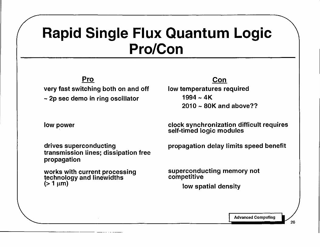
Rapid Single Flux Quantum Logic Pro/Con
Pro very fast switching both on and off
.... 2p sec demo in ring oscillator
low power
drives superconducting transmission lines; dissipation free propagation
works with current processing technology and linewidths (> 1 Jim)
Con low temperatures required
1994 .... 4K 2010 .... SOK and above??
clock synchronization difficult requires self-timed logic modules
propagation delay limits speed benefit
superconducting memory not competitive
low spatial density
Advanced Computing
Pro-
Rapid Single Flux Quantum Logic Pro/Con
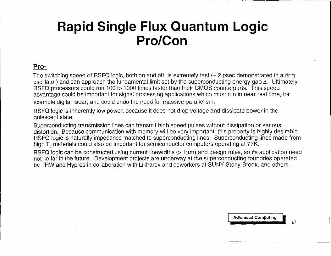
The switching speed of RSFO logic, both on and off, is extremely fast (~ 2 psec demonstrated in a ring oscillator) and can approach the fundamental limit set by the superconducting energy gap~. Ultimately RSFO processors could run 100 to 1000 times faster than their CMOS counterparts. This speed advantage could be important for signal proces~jng applications which must run in near real time, for example digital radar, and could undo the need for massive parallelism.
RSFO logiC is inherently low power, because it does not drop voltage and dissipate power in the quiescent state.
Superconducting transmission lines can transmit high speed pulses without dissipation or serious distortion. Because communication with memory will be very important, this property is highly desirable. RSFO logic is naturally impedance matched to superconducting lines. Superconducting lines made from high Tc materials could also be important for semiconductor computers operating at 77K.
RSFO logiC can be constructed using current linewidths (> 1/J.m) and design rules, so its application need not lie far in the future. Development projects are underway at the superconducting foundries operated by TRW and Hypres in collaboration with Likharev and coworkers at SUNY Stony Brook, and others.
Advanced Computing L. ..... ______ ... 27
Con -
Rapid Single Flux Quantum Logic Pro/Con (concluded)
Low temperatures are required for RSFQ logic. Using the present Niobium technology, liquid He temperatures (T - 4K) are necessary. The computer must be accompanied by a cooler which adds to the size and expense, and limits the application of this technology to high end systems. Suitable closed cycle coolers are currently available for use with cryopumps. In the future, higher temperature operation may become possible if reliable, mass produced, high Te SQUID's are developed.
High speed operation of RSFQ logic requires the use of self-timed logic or related schemes in order to overcome the synchronization problems associated with propagation delay. A similar problem also occurs for fast CMOS logic at - 1 GHz clock speeds. Approaches to self-timed logiC (described in the architecture section) have been developed, but require several times the number of gates as conventional logic.
Propagation delay limits the potential speed benefit of RSFQ logic. Even with a single fast processor, the propagation delay to and from memory would pose a serious problem .. Similar problems also occur for fast CMOS systems. Their solution requires new approaches to managing the physical location of information in memory and new approaches to managing latency, discussed in the architecture section.
Compatible memory is a problem. Superconducting single flux quantum memory is not competitive because it has relatively low spatial density. The area required to trap a flux quantum is large for moderate critical currents: one needs leL> <1>0' the small inductance L associated with small sizes requires greater Ie. Fast memory access is also a problem, and will probably require paging from a larger slower memory to a smaller faster one.
Advanced Computing ~ ,. .............. ' 28

This page intentionally left blank.
Advanced Computing 29

Coulomb Blockade
tunnel junction ~ ~ charge 0
:::>-0 C isolated metal dot ~C
charging energy of dot
circuit model
tunnel junction
-I +
o C
e 2C
gate electrode
+-- number of electrons on dot
V
gate charge Og need not be an integer
minimum energy
I-V characteristic of tunnel junction
----.,...--t---L...----VjUnd
Advanced Computing
Coulomb Blockade
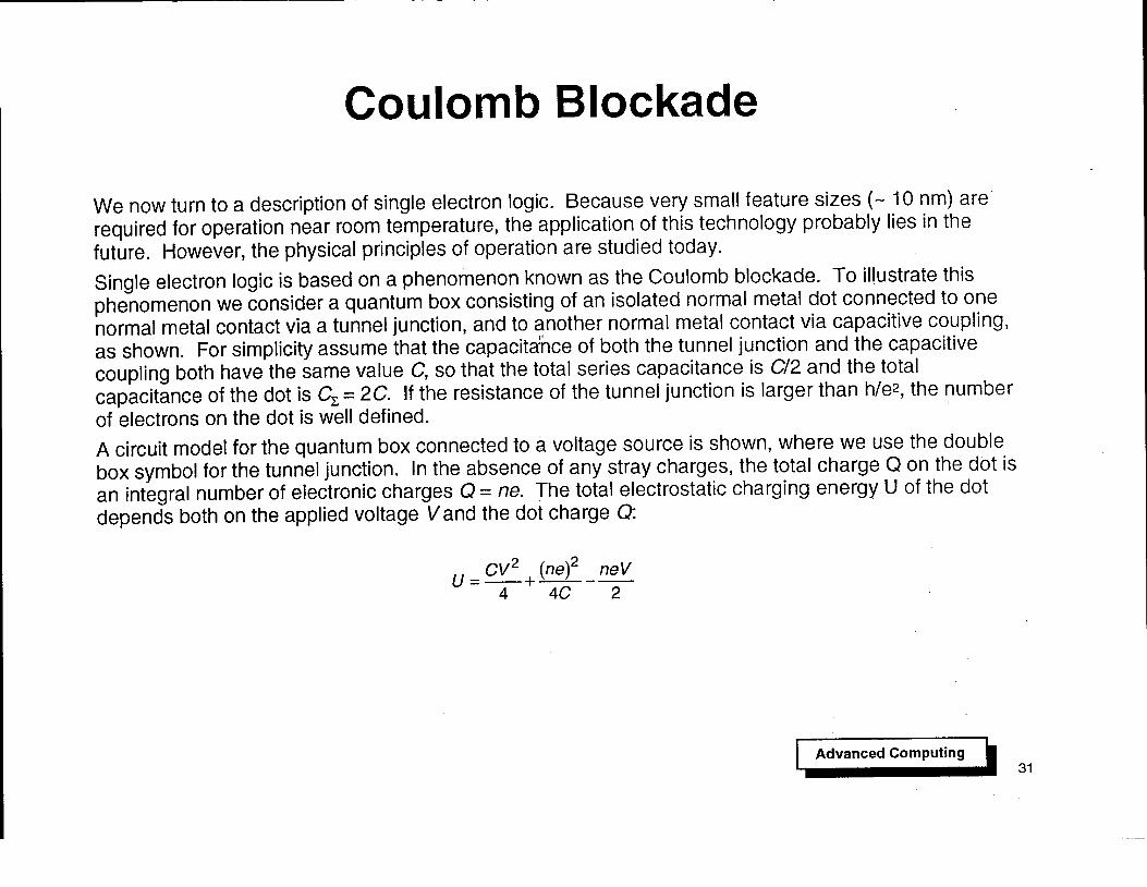
We now turn to a description of single electron logic. Because very small feature sizes (- 10 nm) are required for operation near room temperature, the application of this technology probably lies in the future. However, the physical principles of operation are studied today.
Single electron logic is based on a phenomenon known as the Coulomb blockade. To illustrate this phenomenon we consider a quantum box consisting of an isolated normal metal dot connected to one normal metal contact via a tunnel junction, and to another normal metal contact via capacitive coupling, as shown. For simplicity assume that the capacita!f,ce of both the tunnel junction and the capacitive coupling both have the same value C, so that the total series capacitance is C/2 and the total capacitance of the dot is Cr. = 2C. If the resistance of the tunnel junction is larger than h/e2, the number of electrons on the dot is well defined. . A circuit model for the quantum box connected to a voltage source is shown, where we use the double box symbol for the tunnel junction. In the absence of any stray charges, the total charge Q on the dot is an integral number of electronic charges Q = ne. The total electrostatic charging energy U of the dot depends both on the applied voltage Vand the dot charge Q:
Advanced Computing .. ~ ______ ... 31
Coulomb Blockade (continued)
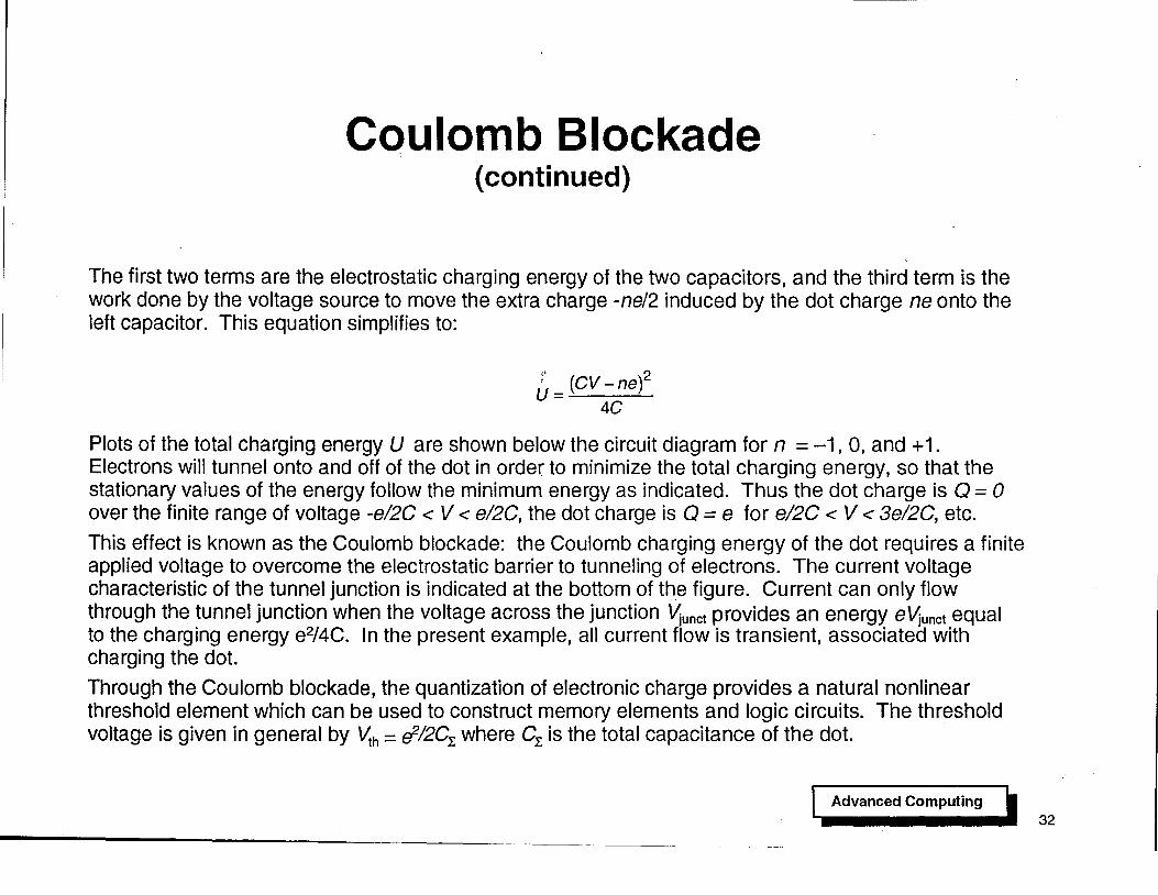
The first two terms are the electrostatic charging energy of the two capacitors, and the third term is the work done by the voltage source to move the extra charge -ne/2 induced by the dot charge ne onto the left capacitor. This equation simplifies to:
~ = (CV _ne)2
4C
Plots of the total charging energy U are shown below the circuit diagram for n = -1,0, and +1. Electrons will tunnel onto and off of the dot in order to minimize the total charging energy, so that the stationary values of the energy follow the minimum energy as indicated. Thus the dot charge is Q = 0 over the finite range of voltage -e12C < V < e12C, the dot charge is Q = e for el2C < V < 3e12C, etc.
This effect is known as the Coulomb blockade: the Coulomb charging energy of the dot requires a finite applied voltage to overcome the electrostatic barrier to tunneling of electrons. The current voltage characteristic of the tunnel junction is indicated at the bottom of the figure. Current can only flow through the tunnel junction when the voltage across the junction Vjunct provides an energy eVJunct equal to the charging energy e2/4C. In the present example, all current flow is transient, associated with charging the dot.
Through the Coulomb blockade, the quantization of electronic charge provides a natural nonlinear threshold element which can be used to construct memory elements and logic circuits. The threshold voltage is given in general by ~h = if12Cr. where Cr. is the total capacitance of the dot.
Advanced Computing '-,. .............. ' 32

Coulomb Blockade (concluded)
In order to observe the Coulomb blockade, the temperature must be low enough that the thermal energy is small compared with the charging energy:
kT < e2/2Cr..
To avoid unwanted switching due to thermal activation, kT must be quite small, a factor of 10 to 100 times smaller than the charging energy. Because the charging energy increases as the size of the device is reduced, smaller devices operate at higher temperatures.
One can make a rough estimate of the temperature of operation by using the fact that the capacitance Cr. is typically dominated by the self-capacitance of the dot. The charging energy Uth is then:
where r is the linear dimension of the dot. For current device sizes r - 100 nm, Uth - 10 meV (100 K) and the maximum operating temperature is Top - 1 K to 10K. As devices become smaller, the operating voltage and temperature increase in proportion to 1/r: for r - 10 nm, Uth - 0.1 eV (1000 K) and the maximum operating temperature is Top - 10K to 100 K, a more convenient range for applications.
Advanced Computing .. ~ ______ ... 33

Single-Electron Transistor
I .- capacitive ---L- gate
Cg
>---p---< met~ ? change tunnel isolated 0 contact metal dot
charging energy
conductance GSd
n=2 n=-1
gate
6 c I I 9
sou~e OJ al OJ dot traps integer number ~ of electronic charges circuit model
U n=O
~ 2
n=2
SET
drain
ultra-sensitive electrometer Og dO ; 104 eHr112
Advanced Computing
Single-Electron Transistor
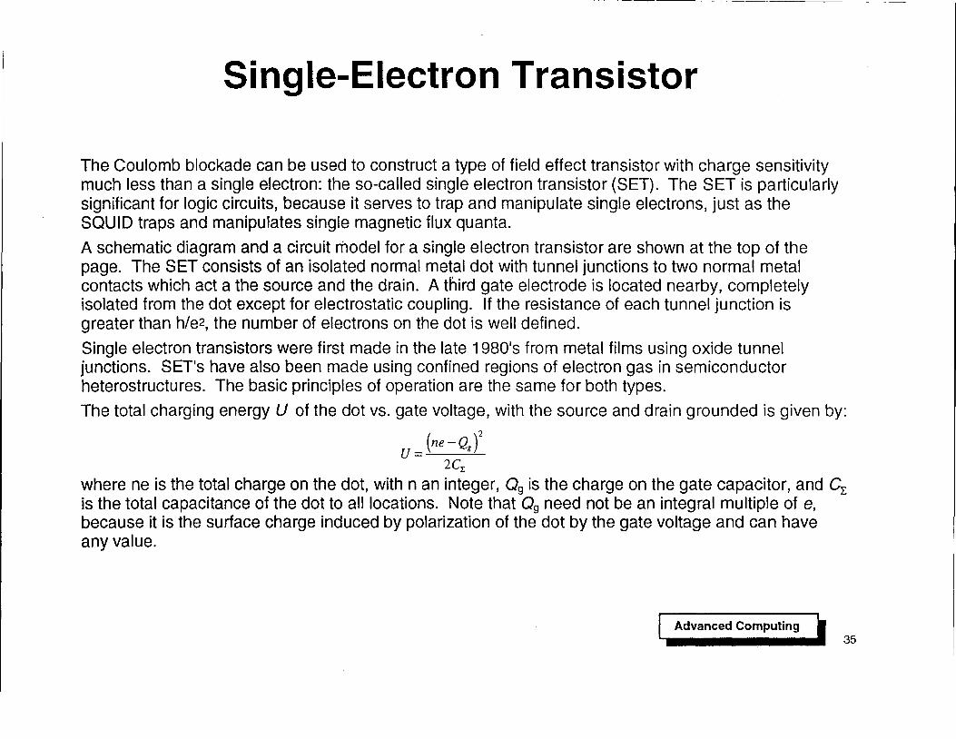
The Coulomb blockade can be used to construct a type of field effect transistor with charge sensitivity much less than a single electron: the so-called single electron transistor (SET). The SET is particularly significant for logic circuits, because it serves to trap and manipulate single electrons, just as the SQUID traps and manipulates single magnetic flux quanta.
A schematic diagram and a circuit model for a single electron transistor are shown at the top of the page. The SET consists of an isolated normal metal dot with tunnel junctions to two normal metal contacts which act a the source and the drain. A third gate electrode is located nearby, completely isolated from the dot except for electrostatic coupling. If the resistance of each tunnel junction is greater than h/e2, the number of electrons on the dot is well defined.
Single electron transistors were first made in the late 1980's from metal films using oxide tunnel junctions. SETs have also been made using confined regions of electron gas in semiconductor heterostructures. The basic principles of operation are the same for both types.
The total charging energy U of the dot vs. gate voltage, with the source and drain grounded is given by:
u = (ne-Qgf 2Cl:
where ne is the total charge on the dot, with n an integer, Og is the charge on the gate capacitor, and CL is the total capacitance of the dot to all locations. Note that Og need not be an integral multiple of e, because it is the surface charge induced by polarization of the dot by the gate voltage and can have any value.
Advanced Computing '-..... ______ ... ' 35
Single-Electron Transistor (concluded)
The Coulomb blockade in this structure provides the mechanism for a very sensitive field effect transistor. A plot of the charging energy U vs. gate charge is shown for several values of n at the middle of the page, and a plot of the source to drain conductance GSD vs. gate charge is shown at the bottom. The charging energy U consists of a family of parabolas, one for each value of n. Adjacent parabolas intersect at half integral values of gate ctfarge Og = [(2n + 1 )/2Je as shown. Near intersections, the total energy U is comparable for nand n + 1 electrons, and the number of electrons on the dot can change, allowing charge to flow from source to drain. Away from the intersections, the energy U is different for different numbers of electrons, and the number of electrons is fixed, preventing the flow of current. Thus the source to drain conductance GSD is peaked at values of gate charge Og = [(2n + 1 )/21e separated by a single electronic charge. This property leads to the name Single electron transistor.
Single electron transistors are impedance converters with large power gain, and they make very sensitive electrometers: charge sensitivity 80 - 10-4 e 1.../ Hz has been achieved at dilution refrigerator temperatures T - 100 mK.
Advanced Computing ~ ,. ________ , 36

This page intentionally left blank.
Advanced Computing ~ "w ______ .. 1 37
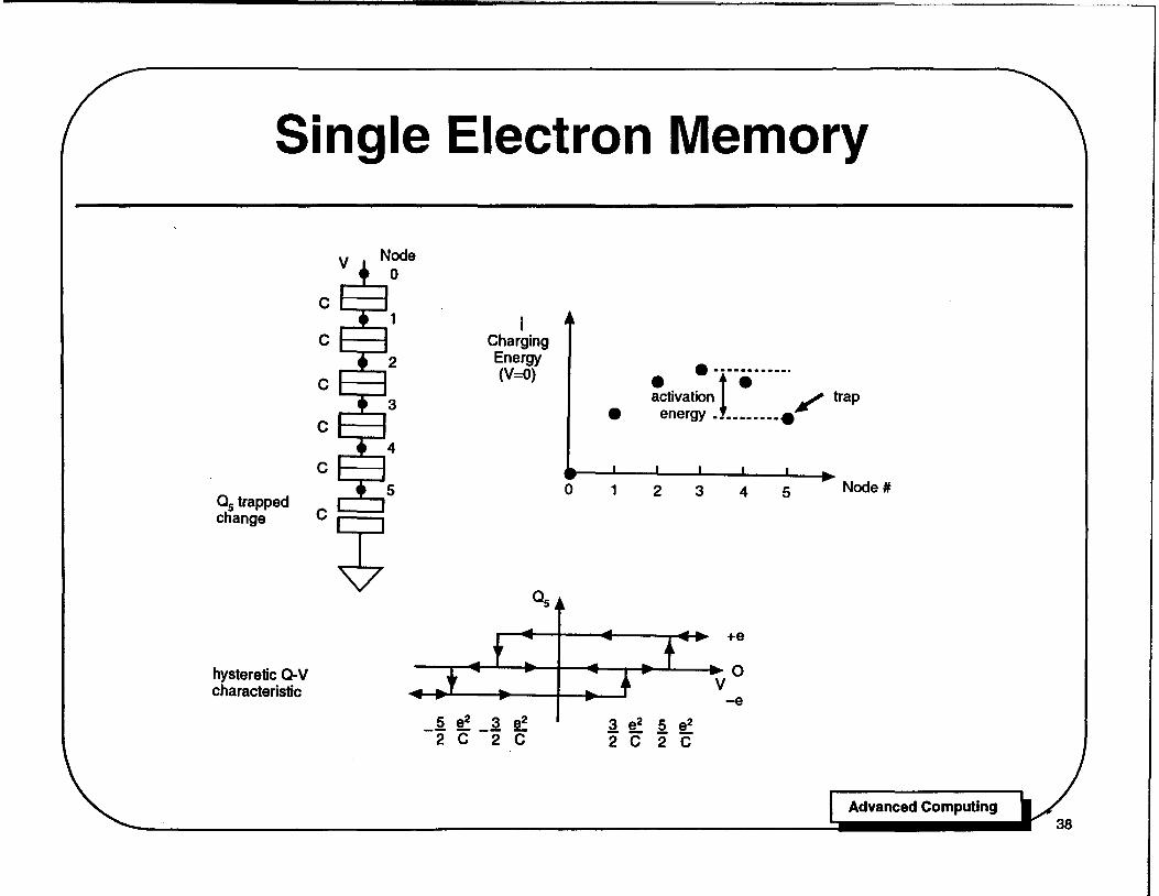
Single Electron Memory
Node 0
C 1 I
C Charging 2 Energy . -_ .... _ .....
(V=O) C • t· 3 •
activation / trap energy ._ •••• _ ••••
C 4
C
5 0 1 2 3 4 5 Node # as trapped
c~ change
as
+e
hysteretic O·V 0 characteristic V
-e 5 e2 3 e2 3 e2 5 e2
-2 C -2 C 2 C 2 C
Advanced Computing
Single Electron Memory
Perhaps the most promising future application for the Coulomb blockade is in single electron memory elements. Dresselhaus et. al. (1994) have demonstrated the operation of a hysteretic Coulomb trap which holds a single electron for times in excess of 2 hours at T = 50 mK. More spectacular results have recently been obtained by workers at Hitachi, who demonstrated a memory element operating at room temperature, based on the single electron prinCiples. The Hitachi device uses a processing trick to achieve very small sizes necessary for room temperature operation - percolating conduction paths in a polysilicon gate. We describe the Stony Brook device below, because its operation is better understood.
The Stony Brook memory element consists of a chain of small normal metal tunnel junctions, as illustrated in the circuit diagram. The chain is broken at one end by a capacitor connected to ground; the other end of the chain is connected to a voltage V. For simplicity we assume all of the junctions and the capaCitor have the same value of capacitance C. Charge can be trapped temporarily on any of the five nodes of the circuit. However, the Coulomb blockade alone is not sufficient to produce a static memory device, because the tunnel junctions leak charge - hysteresis is needed.
One can understand how this chain of junctions traps a single electron by plotting the charging energy &12Cr. necessary to put one electron on a given node of the chain with V = O. Because the total capacitance to ground Or. is a minimum at node 3 in the middle of the chain, the charging energy is a maximum at node 3 and decreases to either side, as shown. An electron placed on node 1 will leave through the top tunnel junction, but an electron placed on node 5 is trapped, because the capacitor cannot pass charge. The depth of the trap is the difference between the charging energy on nodes 5 and 3 as indicated; this activation energy can be increased by using a larger capaCitor from node 5 to ground.
Advanced Computing I _ 39
Single Electron Memory . (continued)
The trap can be loaded and unloaded by changing the voltage V. At the bottom of the page we plot the charge Os on node 5 vs. the applied voltage V, as V is swept above and below zero. As shown, the trapped charge Os at V = 0 depends on the previous history of V, and can have values -e, 0, or +e for the range of voltage indicated. Assume Os and V are initially zero. As V is swept positive, the parabola of charging energy vs. node number is tilted downward at the right, and the energy barrier between nodes 1 and 0 decreases, reaching zero at V = 5e2/2C. At this point a single electron tunnels onto node 1, and rapidly passes through the chain'to nodes at lower energy, finally being trapped on node 5. Once trapped, the electron reduces the potential between nodes 0 and 5, preventing additional electrons from entering the chain. As V is swept downward through zero, the electron remains trapped until the energy barrier between nod,es 4 and 5 is reduced to zero at V = -3e2/2C. At this point the electron leaves and Os returns to zero. Thus the charge vs. voltage curve has a broad and well defined hysteretic region inside which the presence of a trapped electron can be used to represent the state of the memory element.
The presence of an electron in the trap can be sensed nondestructively by using a single electron transistor as an electrometer, or sensed destructively by measuring the presence of a charge pulse as V is swept negative.
Dresselhaus et. al. (1994) have shown experimentally that a trap constructed from seven junctions with R - 300 kQ and C - 0.15 fF holds single electron for more than two hours at T = 50 mK, with a measured activation energy ~U/k - 4K. If this level of performance could be achieved at higher temperatures, it would be useful for practical circuits.
Advanced Computing .. ,. ______ .. 1 40
Single Electron Memory (concluded)
The primary obstacle to the use of single electron memory elements is formidable: the need to construct junctions sufficiently small that the operating temperature is acceptable. In order to achieve operating temperatures - 100 K, junctions smaller than 10 nm are probably required. It is this obstacle which puts the projected use of single electron memory far in the future. However, if one develops sufficiently clever processing tricks to make small junctions, as Hitachi may have, this time frame could be much closer.
Additional factors also need to be considered: co-tunneling, parasitic capacitance, and stray charge.
Co-tunneling of the trapped electron through the entire string of junctions at once limits the trapping time. The co-tunneling rate can be reduced to acceptable values by a suitable number of junctions in series.
Parasitic capacitance reduces the barrier to detrapping and thus the operating temperature.
Coupling to stray charge can cause memory upsets. Present junctions are quite sensitive to the motion of stray charge and to electromagnetic pickup and they must be carefully shielded. However, if junctions can be developed which operate at reasonable temperatures - 100 K and above, the effects of stray charge will be proportionately less important.
Advanced Computing .. ,. ______ .. 1 41
traps flux quantum
«1>0
Duality
SQUID (Superconducting Quantum
Interference Device)
Coulomb Blockade Junction
Vth v
SET (Single Electron Transistor)
traps charge quantum e
0Mm --'----L3-1.L...10-1.L--3'--....I--I.~ Charge ~ -2 -2 2 2
Advanced Computing
Duality
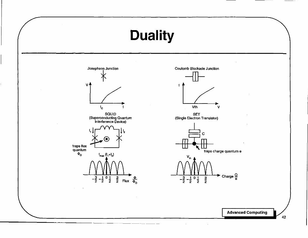
There is an interesting and powerful duality transformation which relates electrical circuits constructed from Josephson junctions to those made from Coulomb blockade junctions. This duality transformation is an extension of the well known duality transformation for passive electrical circuits which exchanges resistors for conductors and capacitors for inductors.
As illustrated, the current voltage characteristics of a Coulomb blockade junction are very similar to the current voltage characteristics of an overdamped Josephson junction, with the axes reversed. The Coulomb blockade junction passes zero current below a threshold voltage \.'.h, while the Josephson junction drops zero voltage below the critical current Ie. Thus the two circuit elements are duals of each other.
Following the rules of the duality transformation in electrical circuit theory, we find that the single electron transistor is the dual of the SQUID: the inductor in the SQUID is transformed into the gate capacitor, and the two Josephson junctions are transformed into two Coulomb blockade junctions. The SQUID traps one quantum of magnetic flux and the SET traps one quantum of electric charge.
This duality extends to the characteristics of the SQUID and SET. The maximum current Imax = 11 + 12 through the SQUID oscillates periodically with the flux <I> in the inductor, as shown, just as the threshold source to drain voltage of the SET for electric conduction oscillates periodically with the gate charge Q.
For every circuit design in RSFQ logic, there exists a dual design in single electron logic with the same equations of motion. For example, the vertical chain of junctions in the single electron memory is similar to the dual of the Josephson junction transmission line in RSFQ logic. This duality is not exploited as much as one might expect, because the dual forms in single electron logic tend to be vertical chains between the power supply rails, a non-standard configuration.
Advanced Computing '-.... ______ ... 43

Single Electron Memory and Logic Pro/Con
Pro
ultimate limit for charge-coupled logic
ultra high packing density _1012 bits per 3x3 cm2 chip
ultra low power
performance improves as size reduced, limited by processing
Con
low temperatures required 1990 -1K 2010 - 100K?
< 10 nm linewidths needed for - 1 OOK operation
high impedance (>100kQ), needs conventional line drivers
stray charge, stray capacitance, and cotunnelling are problems
Advanced Computing

Pro -
Single Electron Memory and Logic Pro/Con
Single electron logic can be regarded as the ultimate limit of charge coupled logic in which a single electron represents one bit. Ultra-high packing density could potentially be achieved once the technology to fabricate ultra-small devices is developed. For example, with - 10 nm linewidths a 3x3 cm2 chip could store - 1012 bits of information. Single electron logic is ultra-low power, because no current is drawn in the quiescent state, and because the energy per bit is very small. For the memory example above, - 10 nm linewidths imply an operating voltage Vop - 0.1 Vand an energy per bit eVop - 10-20 J. The energy stored in the entire chip with 1012 bits is only - 10 111. In contrast to CMOS logic, single electron logic becomes more robust as the size of the devices decreases, and the operating temperature increases.
Con -At present, very low temperatures (-1 K) are required for operation. Extrapolating twenty years in the future, cooling to temperatures < 100K may still be required.
Operation at convenient temperatures - 100K requires device sizes < 10 nm well beyond the projected capability of CMOS foundries in 2010. New processing techniques to produce ultrasmall devices will be necessary. Innovative processing techniques, such as those pursued by Hitachi, may lead to hysteretic memory based on single electron effects much sooner than 2010, if successful.
Advanced Computing .. ...... ______ ... 45
Single Electron Memory and Logic Pro/Con (concluded)
The resistance of Coulomb blockade tunnel junctions must be much greater than hie 2 = 24 kQ in order to define a single electron charge. As a result, single electron devices have high characteristic impedance and are not well suited to driving transmission lines; additional conventional circuitry is required. Stray charge, stray capacitance, and cotunneling are all problems, and their effects on large single electron circuits are not well understood at present.
Advanced Computing ~ ,. ............ ~. 46

Conclusions: 1 Superconducting and Single Electronics .<
Advanced Computing .. ,.. _____ • 47
Conclusions
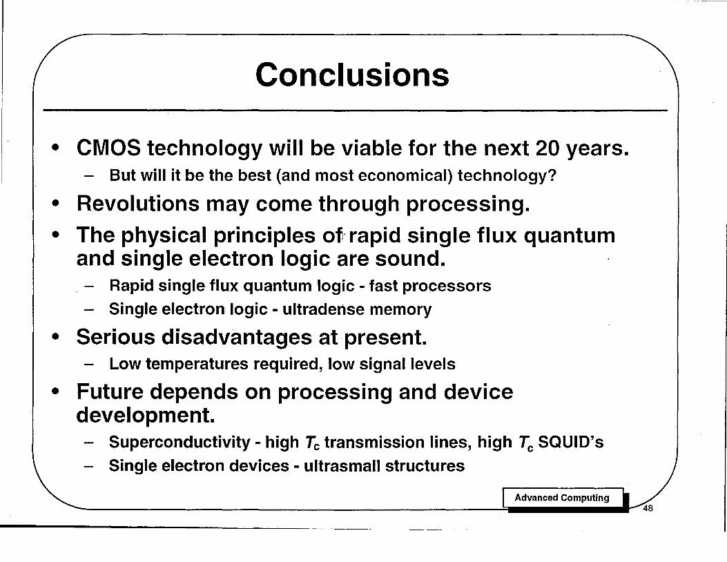
• CMOS technology will be viable for the next 20 years. - But will it be the best (and most economical) technology?
• Revolutions may come through processing.
• The physical principles of~' rapid single flux quantum and single electron logic are sound . . - Rapid single flux quantum logic - fast processors
- Single electron logic - ultradense memory
• Serious disadvantages at ·present. - Low temperatures required, low signal levels
• Future depends on processing and device development. - Superconductivity - high Tc transmission lines, high Tc SQUID's - Single electron devices - ultrasmall structures
Advanced Computing
Conclusions
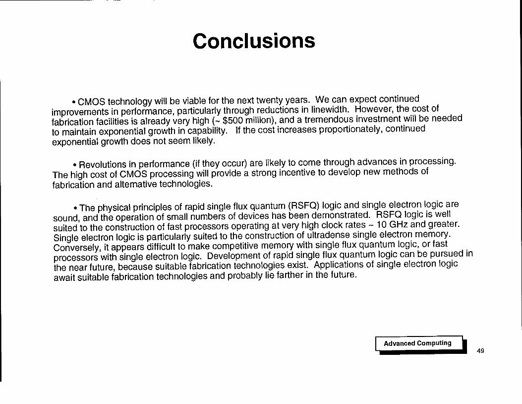
• CMOS technology will be viable for the next twenty years. We can expect continued improvements in performance, particularly through reductions in linewidth. However, the cost of fabrication facilities is already very high (- $500 million), and a tremendous investment will be needed to maintain exponential growth in capability. If the cost increases proportionately, continued exponential growth does not seem likely .
• Revolutions in performance (if they occur) are likely to come through advances in processing. The high cost of CMOS processing will provide a strong incentive to develop new methods of fabrication and alternative technologies .
• The physical principles of rapid single flux quantum (RSFQ) logic and single electron logic are sound, and the operation of small numbers of devices has been demonstrated. RSFQ logiC is well suited to the construction of fast processors operating at very high clock rates - 10 GHz and greater. Single electron logic is particularly suited to the construction of ultradense single electron memory. Conversely, it appears difficult to make competitive memory with single flux quantum logic, or fast processors with single electron logic. Development of rapid single flux quantum logic can be pursued in the near future, because suitable fabrication technologies exist. Applications of single electron logiC await suitable fabrication technologies and probably lie farther in the future.
Advanced Computing .. ,. ______ .. ' 49
Conclusions (Concluded)
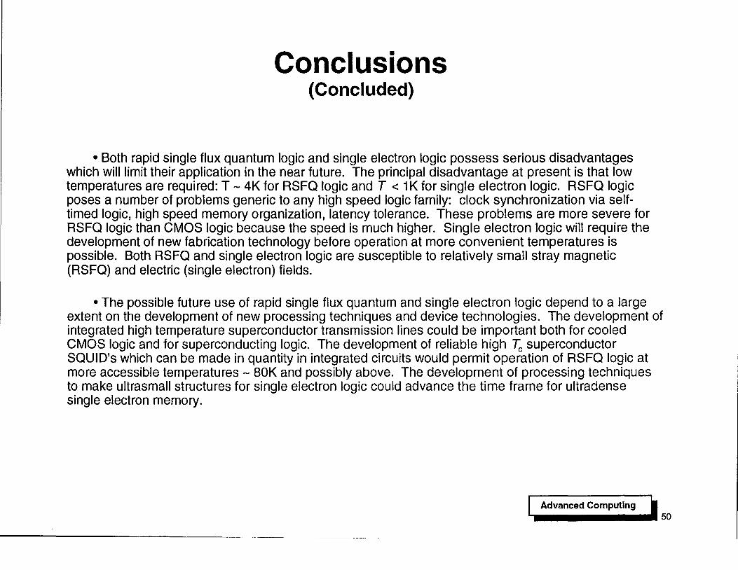
• 80th rapid single flux quantum logic and single electron logic possess serious disadvantages which will limit their application in the near future. The principal disadvantage at present is that low temperatures are required: T - 4K for RSFQ logic and T < 1 K for single electron logic. RSFQ logic poses a number of problems generic to any high speed logic family: clock synchronization via selftimed logic, high speed memory organization, latency tolerance. These problems are more severe for RSFQ logic than CMOS logic because the speed is much higher. Single electron logic will require the development of new fabrication technology before operation at more convenient temperatures is possible. 80th RSFQ and single electron logic are susceptible to relatively small stray magnetic (RSFQ) and electric (single electron) fields.
• The possible future use of rapid single flux quantum and single electron logic depend to a large extent on the development of new processing techniques and device technologies. The development of integrated high temperature superconductor transmission lines could be important both for cooled CMOS logic and for superconducting logic. The development of reliable high ~ superconductor SQUID's which can be made in quantity in integrated circuits would permit operation of RSFQ logic at more accessible temperatures - 8DK and possibly above. The development of processing techniques to make ultrasmall structures for single electron logic could advance the time frame for ultradense single electron memory.
Advanced Computing .. ,. .............. ·50
Advanced Architecture
Advanced Computing .. ..... _____ •• 51

This page intentionally left blank.
Advanced Computing .. ,. .............. ·52

Advanced Architecture
This study addresses high-performance computing in the year 2010 with particular attention to enabling technologies that should be developed in the next five to ten years to lay the groundwork for such machines.
There is a national need for "supercomputers", machines with performance that is five to ten years ahead of high-end desktop systems. These fast computers are needed to solve problems involving nuclear weapons, cryptanalysis, signal processing, and climate modelling. They also have applications in the commercial sector to do seismic analysis, simulate aircraft, automate product design and testing, and "mine" databases of information.
As computer technology changes, interconnection bandwidth is emerging as the limiting factor in the design of high-performance computer systems. The number of floating-point arithmetic operations per second (FLOPS) is becoming far less important than the number of bits per second of bandwidth between the processors, memories, and lID devices in a system. A number of new hardware and software technologies are required to provide the maximum possible bandwidth and to use it most efficiently.
The computer industry is focusing its effort on the rapidly growing market for low-cost desktop and settop systems. While some of the technology of desktop systems can be leveraged for supercomputing, the desktop market does not address the problems of bandwidth and scalability. Architecture technology must be developed in these areas if we are to continue to have viable supercomputing.
Advanced Computing
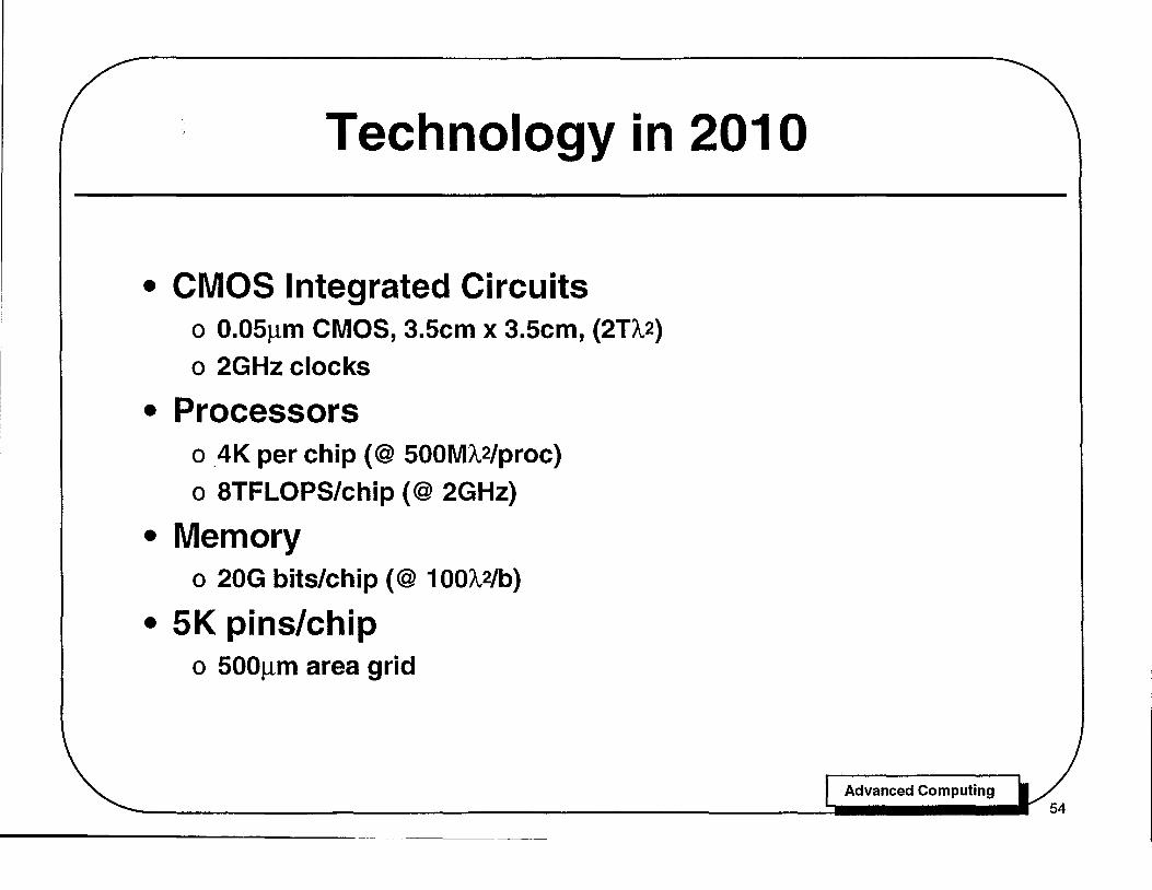
Technology in 201 0
• CMOS Integrated Circuits o O.05~m CMOS, 3.5cm x 3.5cm, (2TA2) o 2GHz clocks
• Processors o .4K per chip (@ 500MA2/proc)
o 8TFLOPS/chip (@ 2GHz)
• Memory o 20G bits/chip (@ 100A2/b)
• 5K pins/chip o 500~m area grid
Advanced Computing
Technology in 2010
Semiconductor Industry Association (SIA) projections of complementary metal oxide semiconductor (CMOS) integrated circuit technology show a continued exponential growth in circuit density and performance through 2007. Extrapolating this data through 2010 we can expect integrated circuits with 1/20 micron (0.05/lm) line widths that are over 3cm across and operate at a 2GHz clock frequency.
Using half the line-width or A as a normalized measure of area, these chips will have an area of 2TA2. If all of this area were devoted to processors, there would be room for 4K 64-bit floating pOint processors with an aggregate performance of 8TFLOPS on a single chip. A chip with this many processors would be useless, however, because of inadequate bandwidth. The same chip area could be used to construct a memory of about 20Gbits. ~
The limiting factor at the chip level, as well as the system level, is bandwidth. On-chip, one can fabricate over 1 OOK wires that run the width of the chip and millions of shorter wires. Off chip, at best one can expect about 5K signal pins. Even with continued improvements in packaging technology, such as multichip modules, it will be difficult to wire 5K pins out from under the 3cm footprint of the chip (a density of 167 wires/mm). Wire density decreases and wire cost increases with distance as one moves through the packaging hierarchy. Thus the system bandwidth will be only a small fraction of the pin bandwidth.
Advanced Computing L. ,. ________ , 55
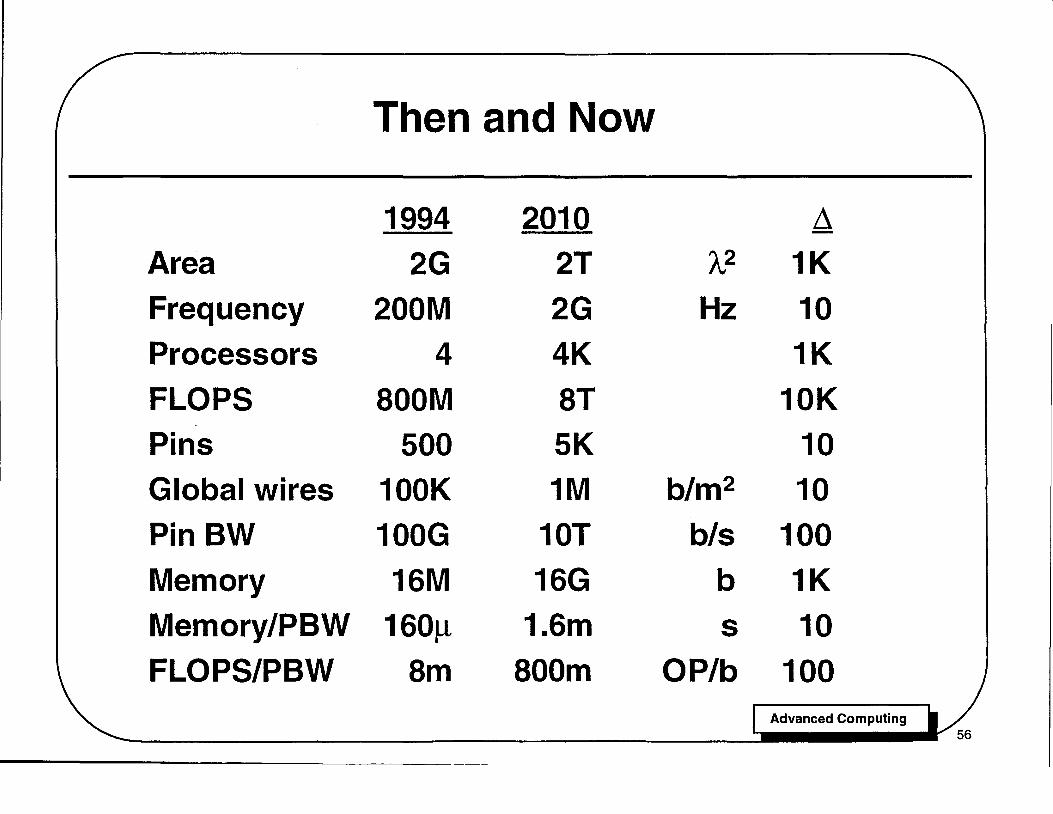
Then and Now
1994 2010 ~
Area 2G 2T "A2 1K
Frequency 200M 2G Hz 10
Processors 4 4K 1K
FLOPS BOOM BT 10K
Pins 500 5K 10
Global wires 100K 1M b/m2 10
Pin BW 100G 10T b/s 100
Memory 16M 16G b 1K
Memory/PBW 160Jl 1.6m s 10
FLOPS/PBW Bm BOOm OP/b 100 Advanced Computing
~---
Then and Now
Comparing projected 201 0 0.05~m CMOS technology to today's 0.5~m CMOS technology shows how non-uniform scaling trends are making communication and parallelism critical issues.
Over the next 16-years, we expect normalized chip area (A. 2) to increase by a factor of 1000. This is due to the 10x smaller linear feature size and to the 3x larger linear die size. Over the same period, clock frequency is expected to increase only by a factor of 10, due to the reduction in feature size. It is clear that most of the performance gain during this period will need to come from parallelism, exploiting the 1000-fold increase in are, since only a factor of 10 can be achieved through circuit speed.
The three components of a computer system: processors, memory, and communication scale at different rates. Processing speed (FLOPS) scale with both frequency and area giving a 10K-fold increase in performance. per unit area over this period. Memory capacity benefits from only area giving a 1 K-fold increase in bits per unit area. Communication bandwidth of both pins and global wires benefit from both density and speed increases but are on a slower density curve and thus increase only by a factor of 100.
The result of this non-uniform scaling is that communication bandwidth between the chips of a system will quickly become the most costly commodity in a computer system. Memory will be of intermediate cost. Processors will be almost free.
Advanced Computing .. ~ ______ ... 57
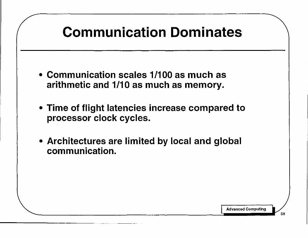
Communication Dominates
• Communication scales 1/100 as much as arithmetic and 1/10 as much as memory.
• Time of flight latencies increase compared to processor clock cycles.
• Architectures are limited by local and global communication.
Advanced Computing
Communication Dominates
Communication will become the dominant factor due to delay as well as cost. As logiC speeds increase, the speed of light remains constant and time-of-flight wire delays will dominate gate delays. Many wires in a large system may be longer than a single clock cycle.
As wire geometries scale down resistivity at high frequencies increases linearly. Higher signalling rates reduce skin depth, and hence increase resistivity, as the square root of frequency. The net result is a 10-fold increase in resistivity per unit length by 2010 which will further increase the cost of communication by making lines more dispersive. Components will need to be packaged close together and lines kept short to achieve high bandwidth over dispersive lines.
To realize cost effective systems, architectures will need to evolve from their present processor-centric state to a communication-centric state in which the design of a system centers around making the most effective use of the available communication bandwidth.
Advanced Computing '-~ ______ ... 59
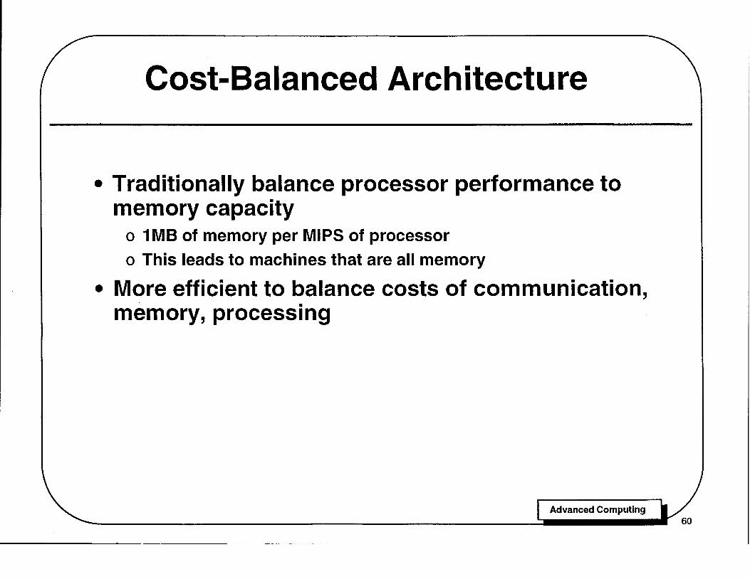
Cost-Balanced Architecture
• Traditionally balance processor performance to memory capacity
o 1 MB of memory per MIPS of processor
o This leads to machines that are all memory
• More efficient to balance costs of communication, memory, processing
Advanced Computing
Cost-Balanced Architecture
To make best use of evolving technology, the balance between processor, memory, and communication in a computer system will need to change to take cost into account.
Today many machines are balanced according to a processor-centric rule-of-thumb coined by Gene Amdahl in the late 1960s which states that for each million instructions per second (MIPS) of processor performance a computer should have a megabyte of memory and a megabit of lID bandwidth. Since memory capacity scales only with density while processor performance scales with both density and frequency, balancing machines this way leads to the majority of cost being in the memory. Already, a typical workstation has less than 1 % of its silicon area, a small fraction of one chip, in the processor (ALU and registers). If machines continue to be balanced in this manner, by 2010 less than 0.1 % of the area will be devoted to processing.
A more effective way to balance machines is by cost. One should add capability in each area (processors, memory, and communications) to the point of equal diminishing returns. For example, increasing the processor to memory ratio of today's machines by a factor of 10, from -1 % to -10%
would be worthwhile if it increases performance by 1 0%.
Today, a relatively small fraction of system cost is devoted to intra-system communication. As communication becomes the performance limiting factor, a larger fraction of cost should be devoted to communication as improvements in this area will have a large impact on performance.
Advanced Computing ~ .... ______ .. ' 61
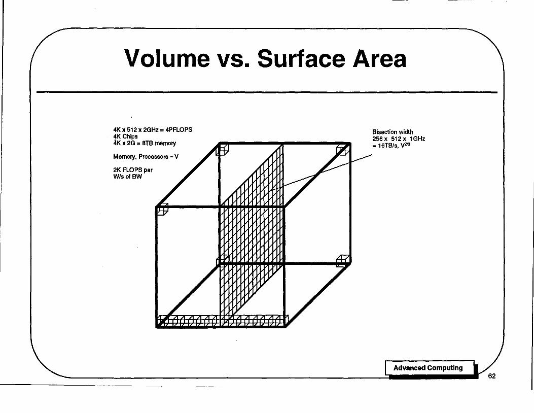
Volume vs. Surface Area
4K x 512 x 2GHz = 4PFLOPS 4K Chips ~K x 2G = 8TB memory
Memory, Processors - V
2K FLOPS per W/sof BW
Bisection width 256 x 512 x 1GHz = 16TB/s, \f213
Advanced Computing
Volume vs. Surface Area
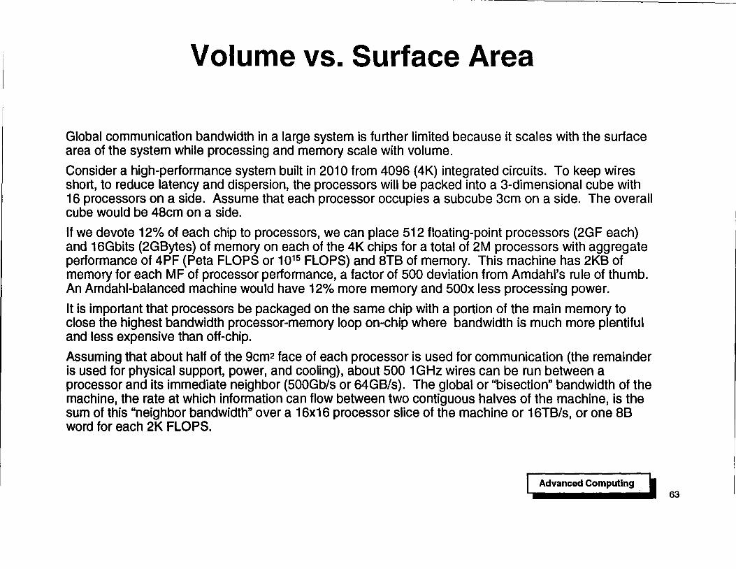
Global communication bandwidth in a large system is further limited because it scales with the surface area of the system while processing and memory scale with volume.
Consider a high-performance system built in 2010 from 4096 (4K) integrated circuits. To keep wires short, to reduce latency and dispersion, the processors will be packed into a 3-dimensional cube with 16 processors on a side. Assume that each processor occupies a subcube 3cm on a side. The overall cube would be 48cm on a side.
If we devote 12% of each chip to processors, we can place 512 floating-point processors (2GF each) and 16Gbits (2GBytes) of memory on each of the 4K chips for a total of 2M processors with aggregate performance of 4PF (Peta FLOPS or 1015 FLOPS) and 8TB of memory. This machine has 2KB of memory for each MF of processor performance, a factor of 500 deviation from Amdahl's rule of thumb. An Amdahl-balanced machine would have 12% more memory and 500x less processing power.
It is important that processors be packaged on the same chip with a portion of the main memory to close the highest bandwidth processor-memory loop on-chip where bandwidth is much more plentiful and less expensive than off-chip.
Assuming that about half of the 9cm2 face of each processor is used for communication (the remainder is used for physical support, power, and cooling), about 500 1GHz wires can be run between a processor and its immediate neighbor (500Gb/s or 64GB/s). The global or "bisection" bandwidth of the machine, the rate at which information can flow between two contiguous halves of the machine, is the sum of this "neighbor bandwidth" over a 16x16 processor slice of the machine or 16TB/s, or one 8B word for each 2K FLOPS.
Advanced Computing .. ~ ______ .' 63

Uniform BW Architecture Does Not Scale
• Global bandwidth scales as V2f3 • 0.006% of silicon provides processing to match BW
'\
MM ••• M
Uniform BW Switch
•••
8TBMemory
16TB/s Bisection Width
2TFLOPS Processing (1 FLOP/Word)
Advanced Computing

Uniform BW Architecture Does Not Scale
Uniform-bandwidth machines have equal bandwidth between every processor and every location of main memory. Such machines, like the Cray YMP and C-90, are popular because they free the programmer from the burden of data placement. All memory locations are equidistant in a bandwidth sense so performance is independent of data placement.
Unfortunately, since access to distant memory is limited by bisection bandwidth, uniformity can be achived only by slowing access to local memory and reducing processing to match the resulting memory bandwidth. In the case of our prototypical 2010 supercomputer, the number of processors would be reduced by a factor of 2000 from 2M to 1 K to provide 1 word of bisection bandwidth (and hence uniform memory bandwidth) per floation-point operation. Instead of having 12% of its area devoted to processing, a uniform bandwidth machine would have only 0.0060/0.
Uniform bandwidth machines are thousands of times less cost effective alternatives because they are processor-centric. They squander expensive bandwidth to keep relatively inexpensive processors busy. A more efficient communication-centric design would use many inexpensive processors to use the expensive communication resources most efficiently.
Advanced Computing L. ~ ______ .. ' 65
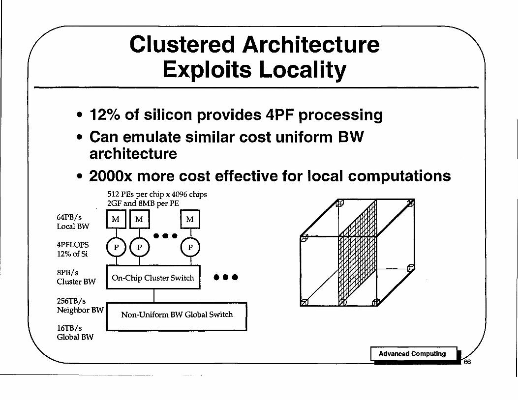
Clustered Architecture Exploits Local ity
• 120/0 of silicon provides 4PF processing
• Can emulate similar cost uniform BW architecture
• 2000x more cost effective for local computations
64PB/s Local BW
4PFLOPS 12%ofSi
512 PEs per chip x 4096 chips 2GF and 8MB per PE
.----. M M M
•••
8PB/s Cluster BW On-Chip Cluster Switch •••
256TB/s NeighborBW
16TB/s Global BW
Non-Uniform BW Global Switch
Advanced Computing
Clustered Architecture Exploits Locality
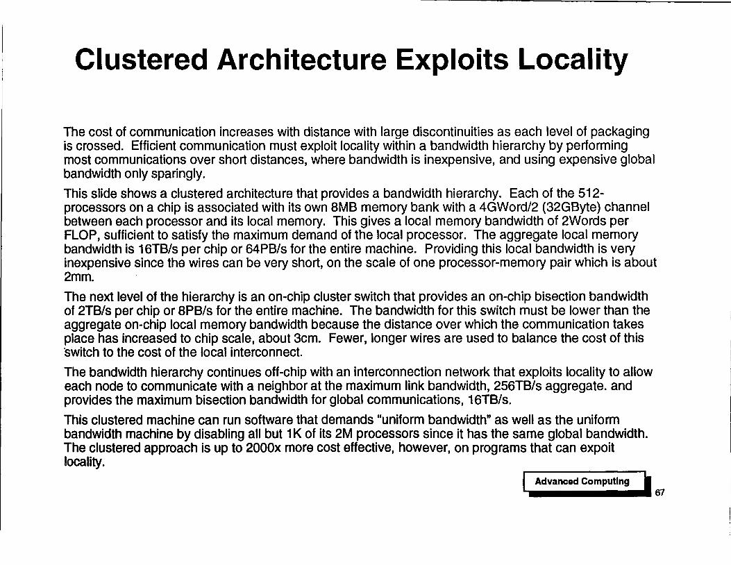
The cost of communication increases with distance with large discontinuities as each level of packaging is crossed. Efficient communication must exploit locality within a bandwidth hierarchy by performing most communications over short distances, where bandwidth is inexpensive, and using expensive global bandwidth only sparingly.
This slide shows a clustered architecture that provides a bandwidth hierarchy. Each of the 512-processors on a chip is associated with its own 8MB memory bank with a 4GWord/2 (32GByte) channel between each processor and its local memory. This gives a local memory bandwidth of 2Words per FLOP, sufficient to satisfy the maximum demand of the local processor. The aggregate local memory bandwidth is 16TB/s per chip or 64PB/s for the entire machine. Providing this local bandwidth is very inexpensive since the wires can be very short, on the scale of one processor-memory pair which is about 2mm.
The next level of the hierarchy is an on-chip cluster switch that provides an on-chip bisection bandwidth of 2TB/s per chip or 8PB/s for the entire machine. The bandwidth for this switch must be lower than the aggregate on-chip local memory bandwidth because the distance over which the communication takes place has increased to chip scale, about 3cm. Fewer, longer wires are used to balance the cost of this switch to the cost of the local interconnect.
The bandwidth hierarchy continues off-chip with an interconnection network that exploits locality to allow each node to communicate with a neighbor at the maximum link bandwidth, 256TB/s aggregate. and provides the maximum bisection bandwidth for global communications, 16TB/s.
This clustered machine can run software that demands "uniform bandwidth" as well as the uniform bandwidth machine by disabling all but 1 K of its 2M processors since it has the same global bandwidth. The clustered approach is up to 2000x more cost effective, however, on programs that can expoit locality.
I Advanced computing, 67
----------------------------------
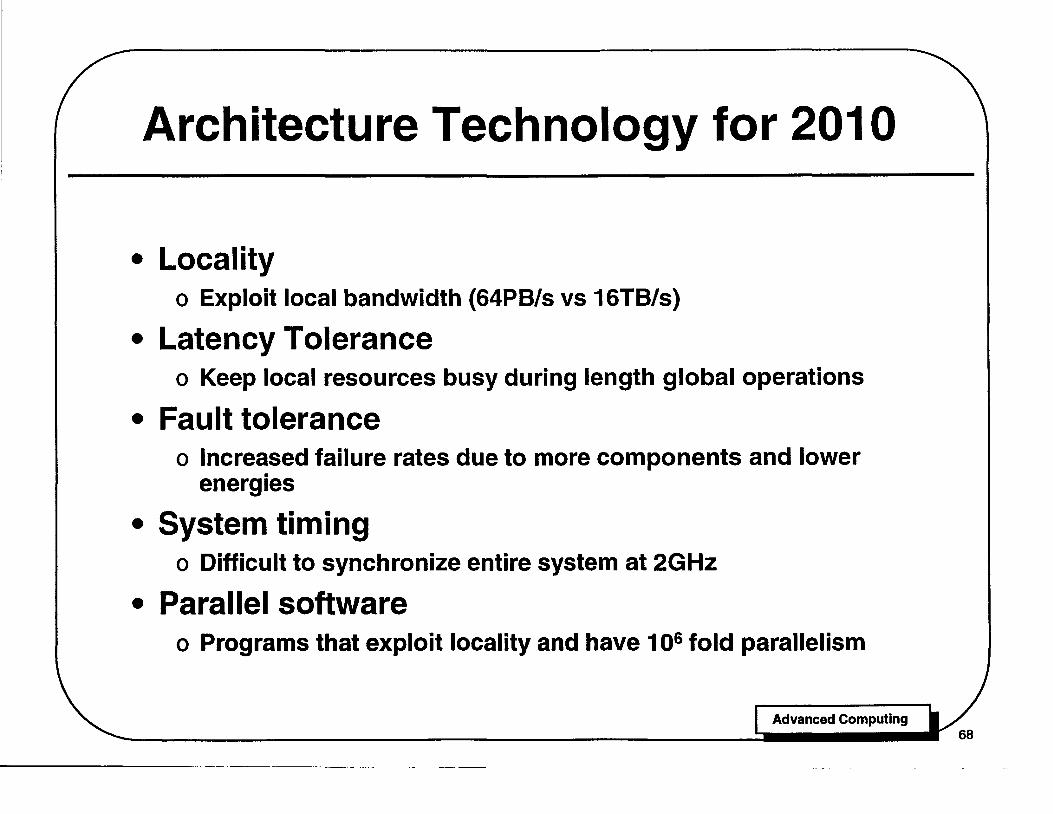
Architecture Technology for 201 0
• Locality o Exploit local bandwidth (64PB/s vs 16TB/s)
• Latency Tolerance o Keep local resources busy during length global operations
• Fault tolerance o Increased failure rates due to more components and lower
energies
• System timing o Difficult to synchronize entire system at 2GHz
• Parallel software o Programs that exploit locality and have 106 fold parallelism
Advanced Computing
Architecture Technology for 2010
To develop supercomputers in 2010 and focus their power on problems of interest will require the development of a number of "architecture technologies" that enable the construction of systems of this scale and address the problem of computing in a bandwidth-efficient manner.
Advanced Computing .. ,............... 69

Exploiting Locality
• Inter-Processor Networks o Provide high "Neighbor" BW o Latency and BW should approach physical limits
• Data placement o Partition data so majority of accesses are local.
o Need 3200:160:16:1 (Local, Cluster, Neighbor, Global)
• Caching o Automatic, coherent management of entire memory can
automatically place and migrate data to exploit locality.
• Limited by communication requirements of algorithms
o e.g., FFT needs O(N) communication for O(NlgN) ops.
Advanced Computing

Exploiting Locality (continued)
One must exploit locality to use bandwidth efficiently. This requires networks that conserve locality in their routing, and efficient methods for data placement to achieve the bounds on information flux required by the underlying algorithm.
The inter-processor network that connects the processing chips in a high-performance system should provide bandwidth and latency that approach the physical limits given available technology. Bandwidthefficient network topologies are well known. However networks today have unacceptably high latencies both due to deep per-node pipelines and high interface overhead. To fully use the available bisection bandwidth, the signalling rates on network links sh<j>uld be pushed to the limits set by the gain-bandwidth product of the semiconductor technology and the attenuation of the transmission medium.
Data placement and migration technology is needed to store data near where it is to be used and to move it to its next point of use in antiCipation of demand. The problem is analgous to the materials flow and inventory problem in manufacturing. A part (number) must be shipped to an assembly plant (processor) at the appropriate time. Too early and storage resources are overwhelmed, too late and the assembly line is stopped waiting for the part.
Data placement is largely a compiler problem. Compilers today either ignore the locality problem (a uniform memory model) or handle all-or nothing locality (the data is either local or somewhere else), e.g., by blocking loops for cache performance. To effiCiently manage bandwidth in our prototypical 2010 system with four levels of locality that have a 3200:1 bandwidth range requires a more comprehensive approach. Compilers must evolve to become bandwith oriented, placing computations to balance load and minimize communications and then scheduling the use of scarce network resources to move data between regions of the memory system to make it available when needed. Compilers must evolve from scheduling instructions and aSSigning registers on the small scale to scheduling network links and assigning memory regions globally.
Advanced Computing I. ..... ______ .. ' 71

Exploiting Locality (concluded)
The appropriate hardware-software tradeoffs must be made in dealing with the data placement problem. Caching can simplify much of the bookkeeping associated with data movement may coherently managing the data name space. The reactive caching practiced today in which data is not requested until it is needed, however, is by itself inadequate. This is analogous to not ordering a part until the assembly line is stopped waiting for it. Also, while caching moves the data it does not address the problem of plaCing the computations. A mix of hardware mechanisms for managing data movement and coherence and software methods for placing computations and initiating transfers are needed to solve this problem.
The communication complexity of algorithms sets a lower bound on the bandwidth required by many problems. For example, an N-point fast Fourier transform (FFT) requires O(N) global communication as every output is affected by every input. With O(NlogN) operations, FFTs are communication-limited for practical problem sizes ( N < about 23200), arithmetic resources will be idled waiting on the limited global communication regardless of how well the compiler or programmer schedule the problem. This does not mean that our machine should have fewer arithmetic resources. This would reduce performance on other problems without significantly reducing cost or improving performance on the FFT. To achieve generality, the resource mix should be cost balanced, not tuned to the needs of a single algorithm.
Advanced Computing .. ...... ______ .. ' 72

This page intentionally left blank.
Advanced Computing '-~ ______ ... 73

Tolerating Latency
• Keep local resources busy while waiting for global requests
• Multithreading o Multiplex several "virtual processors" on hardware
o .Zero-cost context switch when waiting o Requires excess parallelism to cover latency
Pex = Max{1, T x g)
• Pipelined memory system o Memory system must support many outstanding requests o Flow-control required to avoid deadlockllivelock
Advanced Computing

------------------------
Tolerating Latency
Hardware and software technology is required to tolerate the long latencies required of global communication. Even with good management of locality, a global operation on our prototypical 2010 machine will take 1 ODDs of cycles. To efficiently use resources, local operations must continue while waiting for the completion of global operations.
Multithreading is a promising technology for latency tolerance in which several threads or processes interleave their execution on each processor. If on~ thread blocks waiting for completion of a global operation, the other threads continue performing local operations. To use storage efficiently, the threads should not, in general, be unrelated tasks, but rather should be local and global components of the same task.
Multithreading presents several challenges to hardware and software designers. Hardware must be developed that efficiently multiplexes resources over multiple threads. This requires duplication of pipeline state to perform "zero-cycle" context switches when a thread blocks and new techniques to handle pipeline interlocks for communication between threads. Software is needed to organize the computation into threads that overlap execution and to schedule operations in a manner that ensures that there are sufficient local operations to perform to cover anticipated latencies.
At a given point of time, our prototypical 2010 computer system may have millions of outstanding memory operations in flight. New techniques are required to construct memory systems to service these operations and return each result to the appropriate requestor. In particular flow-control methods must be developed to prevent surges in requests to a particular region from overwhelming storage resources and causing deadlock or live lock.
Advanced Computing ~ .... ______ .. ' 75

Fault Tolerance
• Higher component failure rates expected o Failure rates go up as energy levels go down o More total components
• Use ECC to mask soft failures o Memory and communication
• Use redundancy and self-checking design for hard failures
o Processors
• Issue is one of scale o duplicate processors, not gates or ALUs - simpler integration
o Use SW techniques with HW self-checking o Provide high reliability where needed and avoid cost when not
needed.
Advanced Computing

Fault Tolerance
Our prototypical 2010 computer because of its scale and the low energy levels it operates at will see a much higher rate of soft failures than is commonplace today. Even for non-critical applications, such a computer must be designed to tolerate failures without interruption. The large quantitative difference in failure rates requires a qualitative change in methods used to address faults.
We expect that error control codes (ECC) will be used to mask soft errors for non-transforming operations: storage and communication. ECC is already in common use today for memory correction. While it is straightforward to exend the use of ECC to the "payload" component of communication, some care is required to correct the "headers" of packets to prevent errors from resulting in misroutings and to avoid the need to decode and encode on every hop of a network.
To handle hard failures and transforming operations, redundance and self-checking can be employed. Critical state is duplicated in memories that have uncorrelated failure modes and two (or more) processors perform critical tasks periodically cross-checking. With appropriate hardware hooks to maintain synchronization, duplicate communications traffic, and assist with self-checking, this faulttolerance can largely be implemented in software. This will permit the degree of reliability to be tailored to the problem at hand. Very high reliability can be achieved where needed while low-cost simplex operation can be used for non-critical tasks.
Advanced Computing .. ~ ______ .'n

System Timing
• Hard to synchronize entire system at 2GHz
• Plesiochronous signalling (piecewise synchronous)
• Self-timed logic
ClkA ClkAQ ClkB
A
2GHz
B
A lAND) B
Al
AD
Bl
BO
C
Advanced Computing
Cl
CO

System Timing
New approaches are required to synchronize a system with the scale and speed of our prototypical 2010 computer. At 2GHz it will be difficult to distribute a clock to an entire 3cm chip, let alone to a 2M processor system. Alternatives to synchronous operation should be explored to avoid the costs and performance penalties associated with high-speed synchronous operation.
An evolutionary approach is to build piecewise synchronous systems in which small regions of the system, perhaps individual processors, operate synchronously with indpendent clock oscillators. Synchronization is then necessary at the interfaces between regions. One approach involves using a control network to lock the regional oscillators in-phase. More conservative approaches limit the frequency difference between oscillators and use "plesiochronous" synchronizers to retime data travelling between regions. Such constrained synchronization can be performed with no danger of synchronization failure.
A more radical approach to the synchronization problem is to build a self-timed system in which every operation signals its completion. In such a system an operation is performed as soon as all data is available. Granularity is one issue with self-timing. At one extreme, individual gates (such as the AND gate shown above) can be made self-timed, while at the other extreme, this interface is provided only for large modules such as ALUs or whole processors which are implemented internally using conventional techniques. Another issue is whether completion signals should be generated in a delay-insensitive manner or by the use of matched-delay components. USing delay insensitive completion indication (as with the gate above) ensures reliable operation regardless of process variations, but incurs a large expense in gate count and area.
Advanced Computing .. ~ ______ ... 79
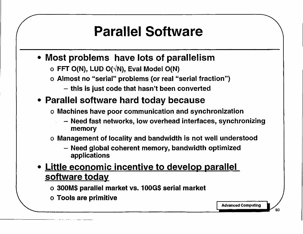
Parallel Software
• Most problems have lots of parallelism o FFT O(N), LUD O("N), Eval Model O(N) o Almost no "serial" problems (or real "serial fraction")
- this is just code that hasn't been converted
• Parallel software hard today because o Machines have poor communication and synchronization
. - Need fast networks, low overhead interfaces, synchronizing memory
o Management of locality and bandwidth is not well understood - Need global coherent memory, bandwidth optimized
applications
• Little economic incentive to develop parallel software today
o 300M$ parallel market vs. 100G$ serial market
o Tools are primitive Advanced Computing
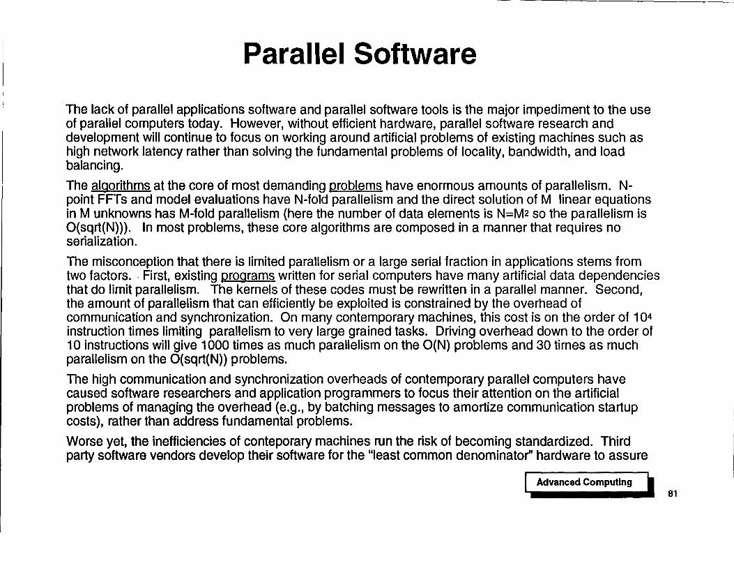
Parallel Software
The lack of parallel applications software and parallel software tools is the major impediment to the use of parallel computers today. However, without efficient hardware, parallel software research and development will continue to focus on working around artificial problems of existing machines such as high network latency rather than solving the fundamental problems of locality, bandwidth, and load balancing.
The algorithms at the core of most demanding problems have enormous amounts of parallelism. Npoint FFTs and model evaluations have N-fold parallelism and the direct solution of M linear equations in M unknowns has M-fold parallelism (here the number of data elements is N=M2 so the parallelism is O(sqrt(N»). In most problems, these core algorithms are composed in a manner that requires no serialization.
The misconception that there is limited parallelism or a large serial fraction in applications stems from two factors .. First, existing programs written for serial computers have many artificial data dependencies that do limit parallelism. The kernels of these codes must be rewritten in a parallel manner. Second, the amount of parallelism that can efficiently be exploited is constrained by the overhead of communication and synchronization. On many contemporary machines, this cost is on the order of 104
instruction times limiting parallelism to very large grained tasks. Driving overhead down to the order of 10 instructions will give 1000 times as much parallelism on the O(N) problems and 30 times as much parallelism on the O(sqrt(N» problems.
The high communication and synchronization overheads of contemporary parallel computers have caused software researchers and application programmers to focus their attention on the artificial problems of managing the overhead (e.g., by batching messages to amortize communication startup costs), rather than address fundamental problems.
Worse yet, the inefficiencies of conteporary machines run the risk of becoming standardized. Third party software vendors develop their software for the "least common denominator" hardware to assure
Advanced Computing L. .... ______ .. ' 81

Parallel Software (concluded)
portability to the maximum number of platforms. Today this means performing communication and synchronization using message passing libraries (like PVM or MPI) and structuring programs to assume the worst possible overheads. Computer manufacturers, in turn, tune the next generation machines to these least-common-denominator applications which reinforces the problems of existing machines.
To break out of this "death-spiral" of parallel overhead requires two developments. First, computer manufacturers must be pushed to eliminate the artificial overheads associated with communication and synchronization. By providing fast networks, low-overhead network interfaces; synchronizing memory, and coherent shared address spaces. Manufacturers can bring down the cost of communicating and synchronizing to within a small factor of the physical limit while eliminating much of the bookkeeping required, for example to provide coherence in software.
Second, parallel software researchers should be redirected to focus on fundamental problems such as load balance, data placement, and data migration. The emphasis needs to be on development of new, enabling technologies for parallel computers rather than force-fitting sequential techologies. For example, operating systems research should address fundamental problems such as managing spatially distributed memory and processing resources. This requires a ground-up redesign of the operating system and cannot be accomplished by porting a sequential operating to each node of a parallel computer. Compatibility with existing sequential software should be preserved by keeping the standard operating system API, not trying to run the same code.
At the root of the problem is a lack of commercial interest in parallel computer software and parallel computing in general. While the sequential computer business (hardware) is a $100 billion/year business, large-scale parallel computing is a $300 million/year business. As a result, industry devotes few resources to developing tools, systems software, or applications for parallel computers. Much like a poor relation, parallel computing gets the hand-me-down systems and application programs which often don't fit well.
Advanced Computing .. ~ ______ .. ' 82

This page intentionally left blank.
Advanced Computing 83

Market Trends Warp Technology Direction
• Desktop/Settop systems drive technology o Develops
- process technology
- processor designs
- memory designs
- small-scale software 2TB/s BW
o I"gnores scalability 200GF
- global packaging technology - latency hiding mechanisms 2TB/s
FlatBW
- fault tolerance
- timing technologies
- scalable software
lOOPEs per chip x 1 chip 2GF and 40MB per PE
r---'I
M M M
• Invest in what the market ignores - calability
Advanced Computing
Market Trends Warp Technology Direction
Industry focuses its resources on the portions of the market that generate the most revenue. Today the focus is on desktop and settop systems with some attention to medium-sized server computers containing a few to a few 10s of processors. Industry devotes very few resources to large-scale parallel computing.
In developing desktop and settop systems, industry drives technology much of which is also useful for large-scale systems. Semiconductor process technology, processor designs, memory designs, and small-scale software (single node) are all technologies being driven by the low-end computer market that can be used nearly unchanged by large-scale machines.
Industry, however, is not developing the technologies required to scale machines to large numbers of processors and to manage the resulting spatially distributed memory. Methods of packaging large numbers of processors, Signalling and synchronization technologies for high-speed interconnection networks, latency hiding techniques such as multithreading, and scalable systems and applications software are receiving little industry investment.
A prudent research investment strategy is to leverage commercial developments by adopting the processes, processors, memories, etc ... for use in parallel machines and to invest research dollars in complementary areas that are not receiving industry attention. Industry will do a better job than the academic and government research communities in the areas they are addressing so there is little pOint in duplicating these efforts. Researchers should be redirected to work on long-term enabling technologies that industry is ignoring.
Advanced Computing .. ,. .............. ' 85
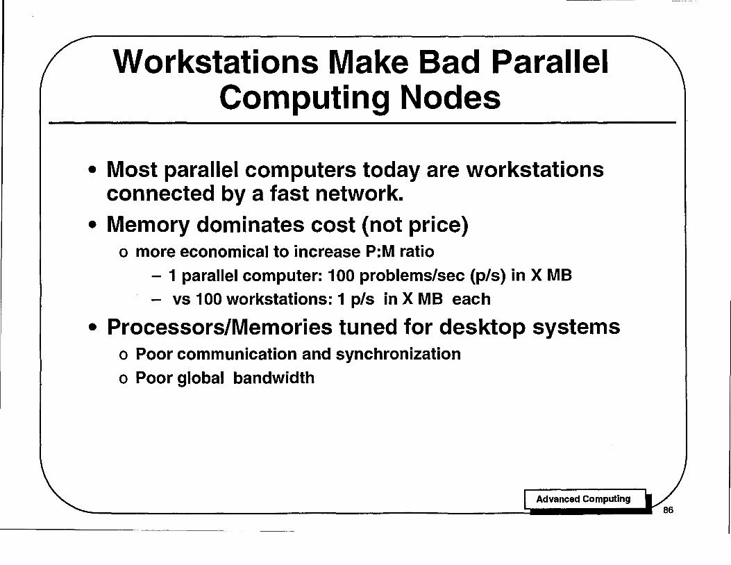
Workstations Make Bad Parallel Computing Nodes
• Most parallel computers today are workstations connected by a fast network.
• Memory dominates cost (not price) o more economical to increase P:M ratio
- 1 parallel computer: 100 problems/sec (p/s) in X MB - vs 100 workstations: 1 pIs in X MB each
• Processors/Memories tuned for desktop systems o Poor communication and synchronization
o Poor global bandwidth
Advanced Computing
Workstations Make Bad Parallel Computing Nodes
Examining a contemporary parallel computer gives a good example of the technology gap in large-scale computing today. Machines such as the Intel Paragon, Thinking Machines CM-5, and Cray T3D are largely collections of workstations connected by a fast network. Because they are manufactured in low volume, they are priced higher than a comparable number of workstations.
By keeping the same processor:memory ratio as a workstation, these machines have forgone the opportunity to offer an improvement in performance/cost through cost balancing. About 80% of the price of a contemporary machine (about 990/0 of the cost) is in the memory. Suppose we have a large set of problems to solve that each require X MBytes of storage and 1 second of compute time on a sequential processor. If we need a throughput of 100 problems/s, it is more cost effective to run the problems one at a time on a 1 DO-processor parallel machine with X MBytes of storage than to run 100 of them simultaneously on 100 X-MByte workstations. In the former case we have duplicated the inexpensive processor (1 % of cost, 20% of price) while in the latter case, we have duplicated the expensive memory system.
Contemporary parallel machines cannot be used in such a configuration, however, because of gaps in available technology. With the exception of the Cray machine, contemporary machines have high network and synchronization overheads and limited network bandwidth which forces them to operate with large granularity. Contemporary machines are run with adaptations of sequential operating systems that require all of the system code and all of the applications code to be duplicated on each node. In many cases this code duplication makes them take more memory, rather than less, to run a set of problems in parallel.
Advanced Computing .. ~ ______ .. ' 87
Workstations Make Bad Parallel Computing Nodes
(concluded)
A relatively small investment in network fabric, network interfaces, and parallel software will close this technology gap. Network technologies can reduce overhead to enable the exploitation of parallelism even on very small problems. A coherent memory shared memory system and restructuring of the systems and application software will allow applications to run without code duplication, permitting a much higher processor to memory ratio. Investments in these areas will be heavily leveraged by complementary industry investment in process, processor, and memory technology.
Unless this technology gap is closed, there will be little performance advantage, and a substantial price disadvantage, of a contemporary parallel computer over a set of workstations connected by a fast localarea-network.
Advanced Computing I-~ ______ ... 88

This page intentionally left blank.
Advanced Computing 89
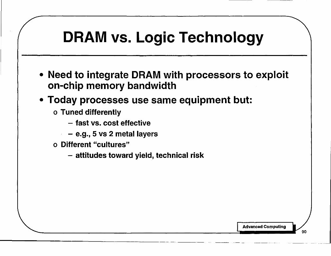
DRAM vs. Logic Technology
• Need to integrate DRAM with processors to exploit on-chip memory bandwidth
• Today processes use same equipment but: o Tuned differently
- fast vs. cost effective
- e.g., 5 vs 2 metal layers o Different "cultures"
- attitudes toward yield, technical risk
Advanced Computing

DRAM vs. Logic Technology
The top two levels of the bandwidth heirarchy, processor-memor, and processor-processor within a cluster, of our prototypical 2010 computer are on-chip. Placing these levels on chip results in much higher aggregate bandwidth than would be possible using off-chip connections (64PB/s vs 256TB/s).
This organization requires integrating the processor and main memory on a single chip so the highbandwidth processor-memory loop can be closed without a chip crossing. While there are no technical bottlenecks to integrating processors on the same chip with high-density memories, there are a number of non-technical hurdles that must be crossed before industry will be prepared to make such a component.
While the same fabrication equipment is used to make logic and memory chips, the processes differ in several ways that reflect different attitudes of the memory and logic "cultures". Memory chips are produced in large volumes with relatively low margins and thus designers are very sensitive to cost and yield. Memory designers are particularly sensitive to the yield of logic outside the array which is usually not protected by redundancy. Logic chips are built in smaller volumes (a typical computer has· 1 processor chip and over 100 memory chips) and so designers are less sensitive to area and yield and more concerned with performance and function. As a result contemporary logic processes typically have more levels of metal (4 or 5 vs 2) and faster devices.
Long before 2010 processors will need to be integrated on-Chip with memories to provide costeffective processor-memory bandwidth. A pilot project is needed to push a manufacturer in this direction in the short term to expose the engineering problems associated with this organization so they can be solved in a timely manner.
Advanced Computing I-..... ______ .' 91

Leveraging Desktop Technology
• Fabrication lines o Desktop/settop invests G$/yr in fabrication facilities o Can be used to manufacture arbitrary components
- in O.5}lm, $10M design cost, $300K tooling charge o Can integrate DRAM and processing
- IBM/Loral Execube o Access can be a problem
• Standard instruction sets o Allow high-end machines to use stock compilers/OSs
. 0 Conservative extensions for communication and synchronization
• Applications software o Binary compatible but not scalable o Incremental path to parallel software
Advanced Computing

Leveraging Desktop Technology
Investment in scalable computing technologies are amplified by making use of technology developed by industry for small-scale systems.
One of industries largest investments is in semiconductor process technology. Manufacturers invest billions per year in advancing technology and constructing new fabrication facilities. These facilities can be used to construct arbitrary components with relatively low design and tooling costs. A typical fullcustom chip can be designed for about $10M with tooling costs of about $300K. As demonstrated by the recent IBM/Loral Execube project, modern processes can integrate processors and high-density DRAM on a single Chip.
One difficulty in leveraging investment in this area is that due to a current shortage in fabrication capacity, it is becoming increasingly difficult to gain access to state of the art fabrication lines for designs that do not represent substantial dollar volumes.
While processors are relatively inexpensive to design, their supporting software is not. The large investment in stock compilers and utility portions of operating systems can be leveraged by providing a standard instruction set with conservative extensions for fast communication and synchronization.
An incremental path must be provided for applications programs to be migrated to scalable machines. By providing compatibility and shared coherent memory, sequential programs can be run on a parallel machine using all of the memory of the machine but without parallelism. A set of tools is then required to incrementally expose parallelism, manage placement, and choreograph data movement. With an incremental approach, the amount of effort invested in a code can be tailored to the amount of performance needed.
Advanced Computing .. ,. ............. ' 93

------------------------------------------------------------------------------
This page intentionally left blank.
Advanced Computing 94
Conclusions: ~'
Advanced Architecture ~
Advanced Computing .. ~ _____ • 95

Conclusions
• Communication dominates architecture o invest in new technologies for communication, e.g.,
superconducting and optical interconnect o uniform bandwidth machines don't scale o clustered architectures exploit locality
• Desktop/settop market drives fabrication technology but ignores scalability
o networks of workstations make poor supercomputers o leverage fabrication technology and software
• Invest in scalability o communication technology
o scalable architecture o parallel software
Advanced Computing
Conclusions
Non-uniform scaling of bandwidth, memory, and arithmetic as technology improves makes the optimum computing architecture for the year 2010 qualitatively different from contemporary computers. Such machines will be bandwidth, rather than arithmetic, limited and thus their architectures and supporting software will be communication rather than processor centric. They will focus on making the best use of the scarce global communication bandwidth.
A prototypical 2010 computer will have non-uniforr!l memory access with a deep bandwidth hierarchy that has a 3200:1 ratio between local and global bandwidth. Such a machine can simulate a uniform memory access machine without loss of performance but can achieve much better performance on programs that can exploit locality.
The prototypical 2010 computer will be cost balanced rather than balanced by a ratio of arithmetic bandwidth to memory capacity.
Industry, through its focus on small-scale systems, will develop much of the process, processor, and memory technology and some of the software required for such systems. However, there is a widening gap in technologies specific to scalable systems that is not being addressed by industry.
To enable scalable systems to be developedin a timely manner, investments must be made to close the gap by investing in technologies that complement rather than duplicate work done in industry. In particular investment is needed in: "
Advanced Computing '-,. .............. ' 97
Conclusions (concluded)
1. High-performance networks and network interfaces to reduce overheads to near physical limits. This includes work on high-speed signalling and synchronization.
2. Architectures that support scalability by tolerating latency, supporting coherent shared memory, providing a deep bandwidth hierarchy, and supporting software strategies for locality.
3. Parallel software technology that addresses fundamental problems of load balance, task placement, and data placement and migration. Technology is also needed to facilitate incremental migration of sequential codes!to parallel machines.
This software technology is dependent on (1) and (2) above to reduce overheads to near physical limits so that software efforts can focus on the real problems of locality and latency and not on artifical problems of inefficient hardware designs.
A relatively small investment in these areas (compared to industry's investment in complementary technology) will lay the groundwork for providing large-scale computers to meet national needs for the coming decades.
Advanced Computing .. ,. ............ ~. 98

This page intentionally left blank.
Advanced Computing 99
DISTRIBUTION LIST
Director of Space and SDI Programs SAF/AQSC 1060 Air Force Pentagon Washington, DC 20330-1060
CMDR & Program Executive Officer US Army/CSSD-ZA Strategic Defense Command PO Box 15280 Arlington, VA 22215-0150
Director Technology Directorate Office of Naval Research Room 407 800 N. Quincy Street Arlington, VA 20305-1000
Dr Albert Brandenstein Chief Scientist Office of Nat'l Drug Control Policy Executive Office of the President Washington, DC 20500
Mr. Edward Brown Assistant Director ARPA/SISTO 3701 North Fairfax Drive Arlington, VA 22203
Dr H Lee Buchanan, I I I Director ARPA/DSO 3701 North Fairfax Drive Arlington, VA 22203-1714
Dr Collier Chief Scientist US Army Strategic Defense Command PO Box 15280 Arlington, VA 22215-0280
DAR P A Library 3701 North Fairfax Drive Arlington, VA 22209-2308
DTIC [2] 8725 John Jay Kingman Road Suite 0944 Fort Belvoir, VA 22060-6218
Mr John Darrah Senior Scientist and Technical Advisor HQAF SPACOM/CN Peterson AFB, CO 80914-5001
Dr Victor Demarines, Jr. President and Chief Exec Officer The MITRE Corporation 202 Burlington Road A210 Bedford,MA 01730-1420
Mr Dan Flynn [5] OSWR Washington, DC 20505
100

DISTRIBUTION LIST
Dr Paris Genalis Naval Warfare Deputy Director OUSD(A&T) /S&TS /NW The Pentagon, Room 3D1048 Washington, DC 20301
Dr Lawrence K Gershwin NIC/NIO/S&T 7E47,OHB Washington, DC 20505
Mr. Thomas H Handel Office of Naval Intelligence The Pentagon, Room 5D660 Washington, DC 20350-2000
Dr Robert G Henderson Director JASON Program Office The MITRE Corporation 1820 Dolley Madison Blvd Mailstop W553 McLean, VA 22102
Dr William E Howard I I I [2] Director of Advanced Concepts & Systems Design The Pentagon Room 3E480 Washington, DC 20301-0103
Dr Gerald J Iafrate U S Army Research Office . PO Box 12211 4330 South Miami Boulevard Research Triangle NC 27709-2211
J A SON Library [5] The MITRE Corporation Mail Stop W002 7525 Coishire Drive McLean, VA 22102
Dr Anita Jones Department of Defense DOD,DDR&E The Pentagon, Room 3E1014 Washington, DC 20301
Mr. 0' Dean P. Judd Los Alamos National Laboratory Mailstop F650 Los Alamos, NM 87545
Dr Bobby R Junker Office of Naval Research Code 111 800 North Quincy Street Arlington, VA 22217
Dr Ken Kress Office of Research and Development 809 Ames Building Washington, DC 20505
Lt Gen, Howard W. Leaf, ( Retired) Director, Test and Evaluation HQUSAF/TE 1650 Air Force Pentagon Washington, DC 20330-1650
101

DISTRIBUTION LIST
Mr. Larry Lynn Director ARPA/DIRO 3701 North Fairfax Drive Arlington, VA 22203-1714
Dr. John Lyons Director of Corporate Laboratory US Army Laboratory Command 2800 Powder Mill Road Adelphi,MD 20783-1145
Col Ed Mahen DARPA/DIRO 3701 North Fairfax Drive Arlington, VA 22203-1714
Dr. Arthur Manfredi OSWR Washington, DC 20505
Mr James J Mattice Deputy Asst Secretary (Research & Engineering), SAF / AQ Pentagon, Room 4D-977 Washington, DC 20330-1000
Dr George Mayer Office of Director of Defense Reserach and Engineering Pentagon, Room 3D375 Washington, DC 20301-3030
Dr Bill Murphy ORD Washington, DC 20505
Mr Ronald Murphy DARPA/ASTO 3701 North Fairfax Drive Arlington, VA 22203-1714
Dr Julian C N all Institute for Defense Analyses 1801 North Beauregard Street Alexandria, VA 22311
Dr Ad Patrinos Director Environmental Sciences Division ER74/GTN US Department of Energy Washington, DC 20585
Dr Bruce Pierce USD(A)D S The Pentagon, Room 3D136 Washington, DC 20301-3090
Mr John Rausch [2] Division Head 06 Department NAVOPINTCEN 4301 Suitland Road Washington, DC 20390
Records Resource The MITRE Corporation Mailstop Wl15 1820 Dolley Madison Blvd McLean, VA 22102
102

DISTRIBUTION LIST
Dr Victor H Reis US Department of Energy DP-1, Room 4A019 1000 Independence Ave, SW Washington, DC 20585
Dr Fred E Saalfeld Director Office of Naval Research 800 North Quincy Street Arlington, VA 22217-5000
Dr Dan Schuresko . O/DDS&T Washington, DC 20505
Dr John Schuster Technical Director of Submarine and SSBN Security Program
Department of the Navy OP-02T The Pentagon Room 4D534 Washington, DC 20350-2000
Dr Michael A Stroscio US Army Research Office P. O. Box 12211 Research Triangle NC 27709-2211
Su perintendent Code 1424 Attn Documents Librarian Naval Postgraduate School Monterey, CA 93943
Ambassador James Sweeney Chief Science Advisor USACDA 320 21st Street NW Washington, DC 20451
Dr George W Ullrich [3] Deputy Director Defense Nuclear Agency 6801 Telegraph Road Alexandria, VA 22310
Dr Walter N Warnick [25] Deputy Director Office of Planning &Analysis, ER-5.1 Office of Energy Research U S Department of Energy Germantown,MD 2074
Dr Edward C Whitman Dep Assistant Secretary of the Navy C3I Electronic Warfare & Space Department of the Navy The Pentagon 4D745 Washington, DC 20350-5000
103