ads58h4x (ads58h40/ads58h43) evm - produktinfo.conrad.com · ads58h4x (ads58h40/ads58h43) evm this...
TRANSCRIPT

User's GuideSLAU455A–August 2012–Revised October 2012
ADS58H4x (ADS58H40/ADS58H43) EVM
This document serves as a user’s guide for the ADS58H4x (ADS58H40/ADS58H43) Evaluation Module(EVM). The EVM provides a platform for evaluating the ADS58H40 or the ADS58H43, a quad-channel,14-bit telecommunications analog-to-digital converter (ADC) operating at sampling rates of up to 250MSPS. Designed for low-power consumption and high spurious free dynamic range (SFDR), the ADC haslow-noise performance and outstanding SFDR over a large input-frequency range.
The four ADC channels are separated into two blocks with two ADCs each. Each block can individually beconfigured into three different operating modes: 11-bit Operating mode, 11-bit SNRBoost mode, 14-bitHigh Resolution Burst mode.
This EVM is ideally suited for mating with the TSW1400 Capture Card for performing a data capture into acapture buffer, uploading the sample data to a PC, performing an FFT, and reporting on SNR, SFDR, andother performance metrics.
For more information regarding the ADS58H4x and the related evaluation tools, please refer to thefollowing:
• ADS58H40 – Quad 14-bit 250-MSPS ADC with SNRBoost and Burst Mode (SBAS589)
• TSW1400 – High-Speed Data Capture and Pattern Generation Platform (SLWU079)
• ADS58H40 EVM Configuration Software (SLAC533). This software is compatible for both ADS58H40and ADS58H43.
Contents1 Introduction .................................................................................................................. 2
1.1 EVM Block Diagram ............................................................................................... 21.2 EVM Power Supply ................................................................................................ 31.3 EVM Connectors and Jumpers ................................................................................... 41.4 EVM ADC Input Circuit Configurations .......................................................................... 6
2 Software Control ............................................................................................................ 72.1 Installation Instructions ............................................................................................ 72.2 Software Operation ................................................................................................ 7
3 Basic Test Procedure ..................................................................................................... 103.1 Test Block Diagram .............................................................................................. 103.2 Test Set-up Connection .......................................................................................... 113.3 ADS58H4x Software Quick Start Guide ....................................................................... 113.4 ADS58H4x and TSW1400 Setup Guide ....................................................................... 11
List of Figures
1 Simplified ADS58H4x EVM Block Diagram.............................................................................. 2
2 Simplified ADS58H4x EVM Power Supply .............................................................................. 3
3 ADS58H4x EVM Connector and Jumper Locations.................................................................... 4
4 ADS58H4x ADC Input Circuit ............................................................................................. 6
5 ADS58H4x Clock Input Circuit ............................................................................................ 6
6 ADS58H4x Main Panel..................................................................................................... 8
7 ADS58H4x SNRBoost/Burst Mode Panel ............................................................................... 9
8 ADS58H4x and TSW1400 Test Setup Block Diagram ............................................................... 10
9 Select ADS58H40 in the High Speed Converter Pro GUI Program ................................................ 12
1SLAU455A–August 2012–Revised October 2012 ADS58H4x (ADS58H40/ADS58H43) EVMSubmit Documentation Feedback
Copyright © 2012, Texas Instruments Incorporated

14-bit ADC
J6
J7
14-bit ADC
J8
J9
J10
14-bit ADC
J11
J12
14-bit ADC
J13
J14
Digital Block
+Output
Formatter
CLKOUTABP/M
DAB[1:13]P/M13
DAB[0]/OVRAB
CLKOUTCDP/M
DCD[1:13]P/M13
DCD[0]/OVRCD
J5
Power SupplyCircuits
USBto
SPI
6 V only
J1
USB
J4
ADS58H4x
CLK IN
CH B
CH C
CH D
CH A
Introduction www.ti.com
10 Load ADC Firmware Prompt ............................................................................................. 12
11 ADS58H4x 11-bit Operating Mode, Single Tone Test Result: Fs = 245.76 MSPS, Fin = 170 MHz............ 13
12 ADS58H4x 11-bit SNRBoost Mode, Single Tone Test Result: Fs = 245.76 MSPS, Fin = 170 MHz........... 14
13 TSW1400 Trigger Option ................................................................................................. 15
14 ADS58H4x 14-bit High-Resolution Mode, Single Tone Test Result: Fs = 245.76 MSPS, Fin = 170 MHz .... 16
List of Tables
1 Power Supply Options...................................................................................................... 3
2 ADS58H4x EVM Connectors .............................................................................................. 4
3 ADS58H4x EVM Jumper Options......................................................................................... 5
4 ADS58H4x EVM Pushbutton Switches .................................................................................. 5
5 ADS58H4x EVM LED Indicators .......................................................................................... 6
1 Introduction
1.1 EVM Block Diagram
Figure 1 shows a simplified block diagram of the default configuration of the EVM. The four analog inputsare supplied to the EVM through a single-ended SMA connection, then transformer coupled, turning thesingle-ended signal into a balanced differential signal, and then input to the ADS58H4x. A dualtransformer input circuit provides better phase and amplitude balance of the input signal when comparedto the performance delivered by a single transformer input circuit.
Figure 1. Simplified ADS58H4x EVM Block Diagram
2 ADS58H4x (ADS58H40/ADS58H43) EVM SLAU455A–August 2012–Revised October 2012Submit Documentation Feedback
Copyright © 2012, Texas Instruments Incorporated
GND
6 V
J2
J3
TPS62420
JP21
TPS7A8001LDO 3.3 V To ADC
To ADC
PWR IN
J1
TPS2400
JP31
JP61
TPS7A8001LDO 1.9 V
JP51
Overvoltage Protection Circuit
Dual OutputDC/DC Converter
Low Noise LDO
Low Noise LDO
www.ti.com Introduction
The clock input is supplied by way of a single-ended signal to an SMA connector and transformer coupledproducing a differential clock signal for the ADS58H4x.
Power to the EVM is typically supplied by a single 6-V power brick. Banana jacks may also be used tosupply power to the EVM. All necessary voltages for the ADS58H4x are derived from the 6-V inputconnection.
1.2 EVM Power Supply
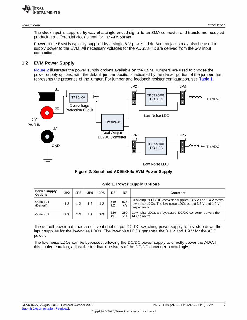
Figure 2 illustrates the power supply options available on the EVM. Jumpers are used to choose thepower supply options, with the default jumper positions indicated by the darker portion of the jumper thatrepresents the presence of the jumper. For jumper and feedback resistor configuration, see Table 1.
Figure 2. Simplified ADS58H4x EVM Power Supply
Table 1. Power Supply Options
Power Supply JP2 JP3 JP4 JP5 R3 R7 CommentOptions
Dual outputs DC/DC converter supplies 3.85 V and 2.4 V to twoOption #1 649 5361-2 1-2 1-2 1-2 low-noise LDOs. The low-noise LDOs output 3.3 V and 1.9 V,(Default) kΩ kΩ respectively.
536 390 Low-noise LDOs are bypassed. DC/DC converter powers theOption #2 2-3 2-3 2-3 2-3 kΩ kΩ ADC directly.
The default power path has an efficient dual output DC-DC switching power supply to first step down theinput supplies for the low-noise LDOs. The low-noise LDOs generate the 3.3 V and 1.9 V for the ADCpower.
The low-noise LDOs can be bypassed, allowing the DC/DC power supply to directly power the ADC. Inthis implementation, adjust the feedback resistors of the DC/DC converter accordingly.
3SLAU455A–August 2012–Revised October 2012 ADS58H4x (ADS58H40/ADS58H43) EVMSubmit Documentation Feedback
Copyright © 2012, Texas Instruments Incorporated

GND PWR IN
ADS58H4x
CLKINCH B
J2J3
J5
J10
J9
J8
J4USB
DNI
J1
CHA
J7
J6
DNI
JP11
1
JP2
JP3
PDN
1
CHC
J11
J12
DNI
J13
J141
JP9SNRB_EN
JP7RESET
JP6
JP5
JP1JP4
1
1
1
1
1
JP12TRIGIN
JP8TRIGRDY
JP10HIRES
SW1RESET
SW2TRIGEN
6VDCD1
USB_PWRD2
D3TRIGRDY
D4HIRE
S
CHD
DNI
LVDS LVDS
Introduction www.ti.com
1.3 EVM Connectors and Jumpers
Figure 3. ADS58H4x EVM Connector and Jumper Locations
The locations of the connectors, jumpers, pushbutton switches, and LEDs are shown in Figure 3. TheEVM has power connectors or banana jacks connecting the main power for power distribution. The SMAconnectors connect the ADC input and ADC clock input to the ADC. Typically, the ADC inputs aretransformer coupled, accepting single-ended connections. The input circuit can be configured to connectto two SMA connectors for differential signaling. Table 2 lists the connector information for the EVM.
Table 2. ADS58H4x EVM Connectors
Reference Designator Description
J1 6 V (main) power input
J2 6 V (main) power input
J3 Ground return
J4 USB Mini-B connector
J5 SAMTEC high-speed LVDS connector
J6 CH A input (positive)
J7 CH A input (negative) DNI
J8 CH B input (positive)
J9 CH B input (negative) DNI
J10 ADC clock input
J11 CH C input (positive)
J12 CH C input (negative) DNI
4 ADS58H4x (ADS58H40/ADS58H43) EVM SLAU455A–August 2012–Revised October 2012Submit Documentation Feedback
Copyright © 2012, Texas Instruments Incorporated

www.ti.com Introduction
Table 2. ADS58H4x EVM Connectors (continued)
Reference Designator Description
J13 CH D input (positive)
J14 CH D input (negative) DNI
The on-board jumper options allow configuration of on-board power supplies and ADC options. Many ofthe jumper selections that involve DC inputs or static control signals are by way of push-on square postjumpers. The jumper options are listed in Table 3. The table indicates the default settings of the jumpersas the EVM is normally shipped. Some of the jumpers are open circuit by default.
Table 3. ADS58H4x EVM Jumper Options
Reference Default OptionalFunction FunctionDesignator Setting Setting
JP1 DNI Connects low-noise LDO (U2) input to main N/Apower input
JP2 1-2 Connects DC/DC converter (U3) output to low- 2-3 Connects DC/DC converter (U3) outputnoise LDO (U2) input directly to the ADC
JP3 1-2 Connects low-noise LDO (U2) output to ADC 2-3 Connects DC/DC converter (U3) outputdirectly to the ADC
JP4 DNI Connects low-noise LDO (U4) input to main N/Apower input
JP5 1-2 Connects DC/DC converter (U3) output to low- 2-3 Connects DC/DC converter (U3) outputnoise LDO (U4) input directly to the ADC
JP6 1-2 Connects low-noise LDO (U4) output to ADC 2-3 Connects DC/DC converter (U3) outputdirectly to the ADC
JP7 2-3 Connects ADC RESET pin G6 to SW1 RESET 1-2 Connects ADC RESET pin G6 to DRVDDswitch
JP8 1-2 Connects ADC TRIG_RDY pin G4 to LED Open ADC TRIG_RDY pin G4 is opencircuit
JP9 2-3 Disables ADC SNRBoost 1-2 Enables ADC SNRBoost
JP10 1-2 Connects ADC HIRES pin G5 to LED circuit Open ADC HIRES pin G5 is open
JP11 2-3 Enables ADC 1-2 Power down the ADC or allows the ADCto standby (configured by CONFIG 0x45,bit D0)
JP12 2-3 Connects trigger signal from SW2 switch to 1-2 Connects trigger signal from TSW1400ADC trigger input. This can be used to start the rev. E to the ADC trigger inputauto-burst process.
There are two pushbuttons on the EVM. While JP7 is set in the 2-3 position, the pushbutton switch, SW1,provides a hardware reset to the ADS58H4x. Upon powering up, the ADC can either accept a hardwarereset by pressing SW1 or by toggling the software reset switch on the EVM GUI. Table 4 lists thedescriptions of each pushbutton switch.
If the ADS58H4x is configured for high resolution burst mode, pressing SW2 while JP12 is set to the 2-3position allows the ADC to enter burst mode. The SW2 pushbutton also provides the initial pulse neededto start the auto-burst mode process after the ADC is configured in High Resolution Auto-Burst mode.
Table 4. ADS58H4x EVM Pushbutton Switches
Reference PurposeDesignator
SW1 While JP7 is set in the 2-3 position, pressing SW1 resets the ADC. The ADC can be reset either by pressingSW1 or with a software reset in the GUI.
SW2 While JP12 is set in the 2-3 position, pressing SW2 allows the ADC to enter burst mode. This can alsoprovide the initial pulse needed start the auto-burst process.
5SLAU455A–August 2012–Revised October 2012 ADS58H4x (ADS58H40/ADS58H43) EVMSubmit Documentation Feedback
Copyright © 2012, Texas Instruments Incorporated

J10CLK IN1:4
0.1 PF
0.1 PF
121�:
121�:
0.1 PF
14-bit ADC
Jp
Jn
0 :
0 :
0 :
0 :
0 :
0 :
0 :
0 :
DNI DNI
DN
ID
NI
DN
I
25�:
25�:0.1 PF 0.1 PF 0.1 PF 0.1 PF
0 :
10 :
10 :
25 :
25�:
82 nH10 pF
3rd Order Bandpass Filter RLR Circuit RLCR Circuit
1:1 1:1
VCM
Introduction www.ti.com
LED D1 is lit indicating the presence of the 6-V supply voltage to the EVM, while LED D2 is lit indicatingthe presence of the USB to serial converter power. LEDs D3 and D4 indicate the status of the ADS58H4xHigh Resolution Burst Mode. Table 5 lists the description of each LED indicator.
Table 5. ADS58H4x EVM LED Indicators
Reference DescriptionDesignator
D1 When lit, D1 shows the presence of the 6-V (main) power supply
D2 When lit, D2 shows the presence of the USB to serial converter power
D3 When lit, D3 indicates that the ADC is ready to enter trigger mode
D4 When lit, D4 indicates that the ADC is in high resolution burst mode
1.4 EVM ADC Input Circuit Configurations
Figure 4 shows the ADS58H4x ADC input circuit. The default setup has a dual 1:1 impedance ratiotransformer input circuit, which achieves better phase and amplitude balance of the input signal than istypically produced by a single transformer input circuit. Third-order bandpass filter component pads areavailable for installing bandpass filter components. The default components for the bandpass filter areeither zero Ω or open circuit.
The default input termination is 50 Ω, which is formed by two 25-Ω resistors connected to the ADC VCMnode. If the user chooses to use 100-Ω termination with the 1:2 impedance transformer, the optional RLRdifferential arm can be used to tune the in-band flatness.
The ADC analog input consists of a switched-capacitor-based, differential sample-and-hold (S/H)architecture. Due to the opening and closing of the sampling glitches, the kick-back noise from the S/Hcircuit may affect the ADC performance. Besides the on-chip R-C filter of the ADC input, the externalRLCR circuit provides additional filtering of the glitches. The default RLCR components have beenoptimized for input bandwidth centered at 185 MHz. For additional RLCR components of different centerfrequencies, refer to the ADS58H40 datasheet (SBAS589).
Figure 4. ADS58H4x ADC Input Circuit
Figure 5 shows the ADS58H4x clock input circuit. The clock signal goes through the 1:4 impedance ratiotransformer increasing the clock amplitude by two (1:4 impedance ratio equals to 1:2 voltage ratio). Thetwo 121-Ω resistors will impedance transform back to the primary side as 50-Ω load impedance for thesignal source generator. For ADC evaluation, set the signal generator output to 10 dBm.
Figure 5. ADS58H4x Clock Input Circuit
6 ADS58H4x (ADS58H40/ADS58H43) EVM SLAU455A–August 2012–Revised October 2012Submit Documentation Feedback
Copyright © 2012, Texas Instruments Incorporated

www.ti.com Software Control
2 Software Control
2.1 Installation Instructions• Open the ADS58H40_Installer_vxpx folder (xpx represents the latest version, which is 2.0 at the time
of this writing)
• Run Setup.exe
• Follow the on-screen instructions
• Once installed, launch by clicking on the ADS58H40_GUI_vxpx program in Start → All Programs →Texas Instruments ADCs
• When plugging in the USB cable for the first time, the Found-New-Hardware-Wizard prompts to installthe USB drivers
– When a pop-up screen opens, select Continue Downloading
– Follow the on-screen instructions to install the USB drivers
– If needed, access the drivers directly in the install directory
2.2 Software Operation
The ADS58H40 EVM GUI is compatible for both ADS58H40 and ADS58H43 EVMs. The software allowsprogramming control of the ADS58H4x device. The front panel provides a tab for common control of theADS58H4x and a SNRBoost/Burst Mode tab for control of the special data capture modes. The GUI tabsprovide a convenient and simplified interface to the most-used registers of each device.
7SLAU455A–August 2012–Revised October 2012 ADS58H4x (ADS58H40/ADS58H43) EVMSubmit Documentation Feedback
Copyright © 2012, Texas Instruments Incorporated

Software Control www.ti.com
2.2.1 Control Options
Figure 6. ADS58H4x Main Panel
8 ADS58H4x (ADS58H40/ADS58H43) EVM SLAU455A–August 2012–Revised October 2012Submit Documentation Feedback
Copyright © 2012, Texas Instruments Incorporated
www.ti.com Software Control
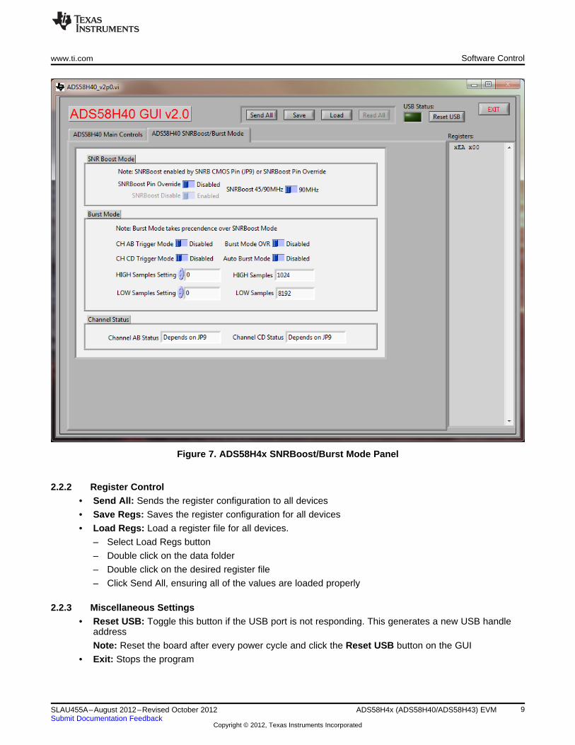
Figure 7. ADS58H4x SNRBoost/Burst Mode Panel
2.2.2 Register Control• Send All: Sends the register configuration to all devices
• Save Regs: Saves the register configuration for all devices
• Load Regs: Load a register file for all devices.
– Select Load Regs button
– Double click on the data folder
– Double click on the desired register file
– Click Send All, ensuring all of the values are loaded properly
2.2.3 Miscellaneous Settings• Reset USB: Toggle this button if the USB port is not responding. This generates a new USB handle
address
Note: Reset the board after every power cycle and click the Reset USB button on the GUI
• Exit: Stops the program
9SLAU455A–August 2012–Revised October 2012 ADS58H4x (ADS58H40/ADS58H43) EVMSubmit Documentation Feedback
Copyright © 2012, Texas Instruments Incorporated
PC
USB
USB J1J4
J5
USB Mini-B
Signal Generator(Input Source)
SignalGenerator
(CLK Source)
CLKJ10CHB
J8
CHAJ6
+5 V
J5
J12
TSW1400
J3
USB Mini-B
CHCJ11
CHDJ13
To A, B, C, D Channels
BPF BPF
SynchronizedSources
+6 V
Basic Test Procedure www.ti.com
3 Basic Test Procedure
This section outlines the basic test procedure for testing the EVM.
3.1 Test Block Diagram
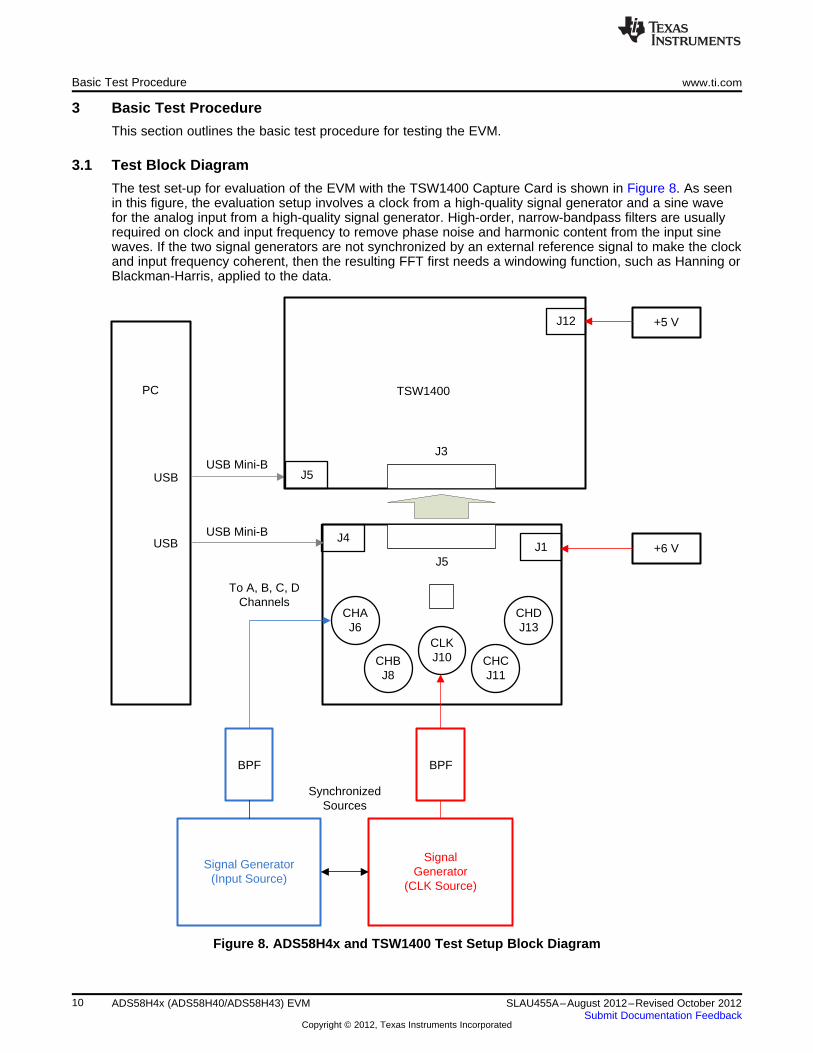
The test set-up for evaluation of the EVM with the TSW1400 Capture Card is shown in Figure 8. As seenin this figure, the evaluation setup involves a clock from a high-quality signal generator and a sine wavefor the analog input from a high-quality signal generator. High-order, narrow-bandpass filters are usuallyrequired on clock and input frequency to remove phase noise and harmonic content from the input sinewaves. If the two signal generators are not synchronized by an external reference signal to make the clockand input frequency coherent, then the resulting FFT first needs a windowing function, such as Hanning orBlackman-Harris, applied to the data.
Figure 8. ADS58H4x and TSW1400 Test Setup Block Diagram
10 ADS58H4x (ADS58H40/ADS58H43) EVM SLAU455A–August 2012–Revised October 2012Submit Documentation Feedback
Copyright © 2012, Texas Instruments Incorporated
www.ti.com Basic Test Procedure
3.2 Test Set-up Connection1. Connect the J5 connector of the EVM to the J3 connector of TSW1400 EVM
2. Connect 5 V to the J12 supply input connector of the TSW1400 and 6 V to the J1 supply inputconnector of the EVM
3. Provide a sample clock at J10 SMA connector of the EVM
4. Provide a sine wave for the analog input at J6, J8, J11, or J13 SMA connectors of the EVM
5. Connect a USB cable from the TSW1400 to the programming computer
6. Connect a USB cable from the EVM to the computer
7. Ensure the initial jumper settings of ADS58H4x, as per Table 3 (if default usage of the ADS58H4x isdesired)
3.3 ADS58H4x Software Quick Start Guide
Figure 6 introduced the front panel of the ADS58H4x SPI GUI. This section covers the initial use of theSPI GUI necessary for most evaluations of the ADS58H4x.
1. Press the Reset USB Port button if the USB connection has been disrupted since last use, or if anerror message pops up warning that the USB connection is not valid.
2. Use the mouse to select the reset position of the reset switch. This switch is self-clearing.
3. Press Send All to send all the register settings.
4. From this point, select digital functions as desired such as SNRBoost, or set test pattern modes ifdesired. All register bits listed in the register map of the ADS58H4x data sheet have a switch on thefront panel of the SPI GUI for easy configuration of the ADS58H4x.
Note that any greyed-out front panel switches are unavailable for use because they have a dependencyupon other switch settings, as indicated in the ADS58H4x datasheet. For example, the Channel A Gainselection is unavailable because the default state of the Channel A Gain Enable switch is off. Select theChannel A Gain Enable switch, toggling the switch to the enabled state, and then the Channel A Gainselection becomes available for use.
3.4 ADS58H4x and TSW1400 Setup Guide
Reference the TSW1400 User’s Guide (SLWU079A) for more detailed explanations of the TSW1400 set-up and operation. This document assumes the High Speed Data Converter Pro software and theTSW1400 hardware are installed and functioning properly. This EVM requires High Speed Data ConverterPro software version 1.5 with TSW1400 hardware of Rev D (or higher).
Single-tone FFT test (ADS58H4x 11-bit Operating Mode)1. Start the High Speed Converter Pro GUI program. When the program starts, select the ADC tab
and then select either the ADS58H40-11b or the ADS58H40-14b device in the Select ADC menu.The selections are compatible for both ADS58H40 and ADS58H43 devices. For this example,select the ADS58H40-11b device.
(a) For 11-bit Operating Mode or 11-bit SNRBoost Mode, select the ADS58H40-11b device.
(b) For 14-bit High Resolution Burst Mode, select the ADS58H40-14b device.
11SLAU455A–August 2012–Revised October 2012 ADS58H4x (ADS58H40/ADS58H43) EVMSubmit Documentation Feedback
Copyright © 2012, Texas Instruments Incorporated

Basic Test Procedure www.ti.com
Figure 9. Select ADS58H40 in the High Speed Converter Pro GUI Program
2. When prompted Do you want to update the Firmware for ADC?, select Yes
Figure 10. Load ADC Firmware Prompt
3. Select Single Tone FFT Test under Test Selection
4. Select the number of sample points (and resulting number of FFT bins). The example shown inFigure 11 has 65536 samples.
5. Enter the ADS58H4x sampling rate. The example shown in Figure 11 has the sample rate set at245.76 MSPS.
6. Enter the input frequency desired. If the clock and input frequency signal generators are synchronized,then make sure the checkbox for coherent frequency is checked and set the input frequency signalgenerator to the input frequency displayed. The example shown in Figure 11 has the input frequencyset at 170 MHz.
7. Select channel A, B, C, or D depending on which channel is connected to the signal generator.
12 ADS58H4x (ADS58H40/ADS58H43) EVM SLAU455A–August 2012–Revised October 2012Submit Documentation Feedback
Copyright © 2012, Texas Instruments Incorporated

www.ti.com Basic Test Procedure
8. Press the Capture button on the High Speed Data Converter Pro GUI.
Observe an FFT result similar to that of Figure 11.
Figure 11. ADS58H4x 11-bit Operating Mode, Single Tone Test Result: Fs = 245.76 MSPS, Fin = 170 MHz
If the basic capture at this point is correct, then the front panel options of the SPI GUI and the front paneloptions of the TSW1400 GUI may be varied. The two examples below show the 11-bit SNRBoost modeand the 14-bit High Resolution Burst Mode.
Single tone FFT test (ADS58H4x 11-bit SNRBoost Mode)1. Select the ADS58H40-11b device.
2. After selecting Single Tone FFT Test under Test Selection, enter the sample rate, input frequency, andthe number of samples.
3. Select channel A, B, C, or D depending on which channel is connected to the signal generator.
4. To enable the SNRBoost Mode, set the JP9 connector to 1-2 position or enable SNRBoost PinOverride in the ADS58H40 GUI. Also, in the ADS58H40 EVM GUI, disable High Resolution BurstMode of the channels under evaluation since High Resolution Burst Mode takes precedence overSNRBoost Mode.
5. Press the Capture button on the High Speed Data Converter Pro GUI.
6. Observe an FFT result similar to that of Figure 12.
7. Select Bandwidth Integration Markers option under Test Options to set the proper integrationcalculation for SNR. Set the bandwidth integration markers, BM0 and BM1, by either dragging themarkers on the FFT screen or by entering the frequency location at the lower left-hand side of the HighSpeed Data Converter GUI.
13SLAU455A–August 2012–Revised October 2012 ADS58H4x (ADS58H40/ADS58H43) EVMSubmit Documentation Feedback
Copyright © 2012, Texas Instruments Incorporated

Basic Test Procedure www.ti.com
Figure 12. ADS58H4x 11-bit SNRBoost Mode, Single Tone Test Result: Fs = 245.76 MSPS, Fin = 170 MHz
Single tone FFT test (ADS58H4x 14-bit High Resolution Burst Mode)1. Select the ADS58H40-14b device.
2. After selecting Single Tone FFT Test under Test Selection, enter the sample rate, input frequency, andthe number of samples.
3. Select channel A, B, C, or D depending on which channel is connected to the signal generator.
4. On the High Speed Data Converter Pro menu, select Data Capture Options → Trigger Option. Checkboth Trigger Mode Enable and Software Trigger Enable.
14 ADS58H4x (ADS58H40/ADS58H43) EVM SLAU455A–August 2012–Revised October 2012Submit Documentation Feedback
Copyright © 2012, Texas Instruments Incorporated

www.ti.com Basic Test Procedure
Figure 13. TSW1400 Trigger Option
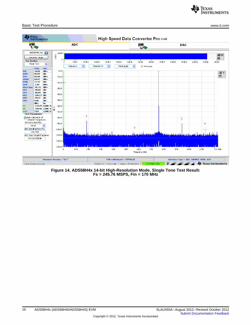
5. In the EVM GUI, enable High Resolution Burst Mode of the channels under evaluation. Set the desiredhigh- and low-resolution samples. The example shown in Figure 14 has both high samples and lowsamples set to maximum. This ensures that the entire FFT is analyzed with 14-bit capture for accurateSNR and SFDR calculations.
6. ADS58H4x Trigger Options
• If the ADS58H4x has auto-trigger enabled, set the J12 jumper to the 2-3 position. Start the auto-trigger process by pressing the SW2 pushbutton.
• TSW1400 Trigger Generation (External Trigger)
– On the EVM, remove the jumper at J12, ensuring the ADS58H4x TRIG_EN (pin G3) is floating.
– Using an SMA to grabber cable, connect SYNC1 SMA connector at J14 of the TSW1400 tojumper J2, pin 2 header of the EVM.
– Using an SMA to SMA cable, connect SYNC3 SMA connector at J16 to EXT_TRIG_INPUTSMA connector at J11 of the TSW1400.
7. Press the Capture button on the High Speed Data Converter Pro GUI.
8. Observe an FFT result similar to that of Figure 14.
15SLAU455A–August 2012–Revised October 2012 ADS58H4x (ADS58H40/ADS58H43) EVMSubmit Documentation Feedback
Copyright © 2012, Texas Instruments Incorporated
Basic Test Procedure www.ti.com
Figure 14. ADS58H4x 14-bit High-Resolution Mode, Single Tone Test Result:Fs = 245.76 MSPS, Fin = 170 MHz
16 ADS58H4x (ADS58H40/ADS58H43) EVM SLAU455A–August 2012–Revised October 2012Submit Documentation Feedback
Copyright © 2012, Texas Instruments Incorporated

EVALUATION BOARD/KIT/MODULE (EVM) ADDITIONAL TERMS
Texas Instruments (TI) provides the enclosed Evaluation Board/Kit/Module (EVM) under the following conditions:
The user assumes all responsibility and liability for proper and safe handling of the goods. Further, the user indemnifies TI from all claimsarising from the handling or use of the goods.
Should this evaluation board/kit not meet the specifications indicated in the User’s Guide, the board/kit may be returned within 30 days fromthe date of delivery for a full refund. THE FOREGOING LIMITED WARRANTY IS THE EXCLUSIVE WARRANTY MADE BY SELLER TOBUYER AND IS IN LIEU OF ALL OTHER WARRANTIES, EXPRESSED, IMPLIED, OR STATUTORY, INCLUDING ANY WARRANTY OFMERCHANTABILITY OR FITNESS FOR ANY PARTICULAR PURPOSE. EXCEPT TO THE EXTENT OF THE INDEMNITY SET FORTHABOVE, NEITHER PARTY SHALL BE LIABLE TO THE OTHER FOR ANY INDIRECT, SPECIAL, INCIDENTAL, OR CONSEQUENTIALDAMAGES.
Please read the User's Guide and, specifically, the Warnings and Restrictions notice in the User's Guide prior to handling the product. Thisnotice contains important safety information about temperatures and voltages. For additional information on TI's environmental and/or safetyprograms, please visit www.ti.com/esh or contact TI.
No license is granted under any patent right or other intellectual property right of TI covering or relating to any machine, process, orcombination in which such TI products or services might be or are used. TI currently deals with a variety of customers for products, andtherefore our arrangement with the user is not exclusive. TI assumes no liability for applications assistance, customer product design,software performance, or infringement of patents or services described herein.
REGULATORY COMPLIANCE INFORMATION
As noted in the EVM User’s Guide and/or EVM itself, this EVM and/or accompanying hardware may or may not be subject to the FederalCommunications Commission (FCC) and Industry Canada (IC) rules.
For EVMs not subject to the above rules, this evaluation board/kit/module is intended for use for ENGINEERING DEVELOPMENT,DEMONSTRATION OR EVALUATION PURPOSES ONLY and is not considered by TI to be a finished end product fit for general consumeruse. It generates, uses, and can radiate radio frequency energy and has not been tested for compliance with the limits of computingdevices pursuant to part 15 of FCC or ICES-003 rules, which are designed to provide reasonable protection against radio frequencyinterference. Operation of the equipment may cause interference with radio communications, in which case the user at his own expense willbe required to take whatever measures may be required to correct this interference.
General Statement for EVMs including a radio
User Power/Frequency Use Obligations: This radio is intended for development/professional use only in legally allocated frequency andpower limits. Any use of radio frequencies and/or power availability of this EVM and its development application(s) must comply with locallaws governing radio spectrum allocation and power limits for this evaluation module. It is the user’s sole responsibility to only operate thisradio in legally acceptable frequency space and within legally mandated power limitations. Any exceptions to this are strictly prohibited andunauthorized by Texas Instruments unless user has obtained appropriate experimental/development licenses from local regulatoryauthorities, which is responsibility of user including its acceptable authorization.
For EVMs annotated as FCC – FEDERAL COMMUNICATIONS COMMISSION Part 15 Compliant
Caution
This device complies with part 15 of the FCC Rules. Operation is subject to the following two conditions: (1) This device may not causeharmful interference, and (2) this device must accept any interference received, including interference that may cause undesired operation.
Changes or modifications not expressly approved by the party responsible for compliance could void the user's authority to operate theequipment.
FCC Interference Statement for Class A EVM devices
This equipment has been tested and found to comply with the limits for a Class A digital device, pursuant to part 15 of the FCC Rules.These limits are designed to provide reasonable protection against harmful interference when the equipment is operated in a commercialenvironment. This equipment generates, uses, and can radiate radio frequency energy and, if not installed and used in accordance with theinstruction manual, may cause harmful interference to radio communications. Operation of this equipment in a residential area is likely tocause harmful interference in which case the user will be required to correct the interference at his own expense.
FCC Interference Statement for Class B EVM devices
This equipment has been tested and found to comply with the limits for a Class B digital device, pursuant to part 15 of the FCC Rules.These limits are designed to provide reasonable protection against harmful interference in a residential installation. This equipmentgenerates, uses and can radiate radio frequency energy and, if not installed and used in accordance with the instructions, may causeharmful interference to radio communications. However, there is no guarantee that interference will not occur in a particular installation. Ifthis equipment does cause harmful interference to radio or television reception, which can be determined by turning the equipment off andon, the user is encouraged to try to correct the interference by one or more of the following measures:
• Reorient or relocate the receiving antenna.• Increase the separation between the equipment and receiver.• Connect the equipment into an outlet on a circuit different from that to which the receiver is connected.• Consult the dealer or an experienced radio/TV technician for help.
For EVMs annotated as IC – INDUSTRY CANADA Compliant
This Class A or B digital apparatus complies with Canadian ICES-003.
Changes or modifications not expressly approved by the party responsible for compliance could void the user’s authority to operate theequipment.
Concerning EVMs including radio transmitters
This device complies with Industry Canada licence-exempt RSS standard(s). Operation is subject to the following two conditions: (1) thisdevice may not cause interference, and (2) this device must accept any interference, including interference that may cause undesiredoperation of the device.
Concerning EVMs including detachable antennas
Under Industry Canada regulations, this radio transmitter may only operate using an antenna of a type and maximum (or lesser) gainapproved for the transmitter by Industry Canada. To reduce potential radio interference to other users, the antenna type and its gain shouldbe so chosen that the equivalent isotropically radiated power (e.i.r.p.) is not more than that necessary for successful communication.
This radio transmitter has been approved by Industry Canada to operate with the antenna types listed in the user guide with the maximumpermissible gain and required antenna impedance for each antenna type indicated. Antenna types not included in this list, having a gaingreater than the maximum gain indicated for that type, are strictly prohibited for use with this device.
Cet appareil numérique de la classe A ou B est conforme à la norme NMB-003 du Canada.
Les changements ou les modifications pas expressément approuvés par la partie responsable de la conformité ont pu vider l’autorité del'utilisateur pour actionner l'équipement.
Concernant les EVMs avec appareils radio
Le présent appareil est conforme aux CNR d'Industrie Canada applicables aux appareils radio exempts de licence. L'exploitation estautorisée aux deux conditions suivantes : (1) l'appareil ne doit pas produire de brouillage, et (2) l'utilisateur de l'appareil doit accepter toutbrouillage radioélectrique subi, même si le brouillage est susceptible d'en compromettre le fonctionnement.
Concernant les EVMs avec antennes détachables
Conformément à la réglementation d'Industrie Canada, le présent émetteur radio peut fonctionner avec une antenne d'un type et d'un gainmaximal (ou inférieur) approuvé pour l'émetteur par Industrie Canada. Dans le but de réduire les risques de brouillage radioélectrique àl'intention des autres utilisateurs, il faut choisir le type d'antenne et son gain de sorte que la puissance isotrope rayonnée équivalente(p.i.r.e.) ne dépasse pas l'intensité nécessaire à l'établissement d'une communication satisfaisante.
Le présent émetteur radio a été approuvé par Industrie Canada pour fonctionner avec les types d'antenne énumérés dans le manueld’usage et ayant un gain admissible maximal et l'impédance requise pour chaque type d'antenne. Les types d'antenne non inclus danscette liste, ou dont le gain est supérieur au gain maximal indiqué, sont strictement interdits pour l'exploitation de l'émetteur.
SPACER
SPACER
SPACER
SPACER
SPACER
SPACER
SPACER
SPACER

【【Important Notice for Users of this Product in Japan】】This development kit is NOT certified as Confirming to Technical Regulations of Radio Law of Japan
If you use this product in Japan, you are required by Radio Law of Japan to follow the instructions below with respect to this product:
1. Use this product in a shielded room or any other test facility as defined in the notification #173 issued by Ministry of Internal Affairs andCommunications on March 28, 2006, based on Sub-section 1.1 of Article 6 of the Ministry’s Rule for Enforcement of Radio Law ofJapan,
2. Use this product only after you obtained the license of Test Radio Station as provided in Radio Law of Japan with respect to thisproduct, or
3. Use of this product only after you obtained the Technical Regulations Conformity Certification as provided in Radio Law of Japan withrespect to this product. Also, please do not transfer this product, unless you give the same notice above to the transferee. Please notethat if you could not follow the instructions above, you will be subject to penalties of Radio Law of Japan.
Texas Instruments Japan Limited(address) 24-1, Nishi-Shinjuku 6 chome, Shinjuku-ku, Tokyo, Japan
http://www.tij.co.jp
【ご使用にあたっての注】
本開発キットは技術基準適合証明を受けておりません。
本製品のご使用に際しては、電波法遵守のため、以下のいずれかの措置を取っていただく必要がありますのでご注意ください。1. 電波法施行規則第6条第1項第1号に基づく平成18年3月28日総務省告示第173号で定められた電波暗室等の試験設備でご使用いただく。2. 実験局の免許を取得後ご使用いただく。3. 技術基準適合証明を取得後ご使用いただく。
なお、本製品は、上記の「ご使用にあたっての注意」を譲渡先、移転先に通知しない限り、譲渡、移転できないものとします。
上記を遵守頂けない場合は、電波法の罰則が適用される可能性があることをご留意ください。
日本テキサス・インスツルメンツ株式会社東京都新宿区西新宿6丁目24番1号西新宿三井ビルhttp://www.tij.co.jp
SPACER
SPACER
SPACER
SPACER
SPACER
SPACER
SPACER
SPACER
SPACER
SPACER
SPACER
SPACER
SPACER
SPACER
SPACER
SPACER

EVALUATION BOARD/KIT/MODULE (EVM)WARNINGS, RESTRICTIONS AND DISCLAIMERS
For Feasibility Evaluation Only, in Laboratory/Development Environments. Unless otherwise indicated, this EVM is not a finishedelectrical equipment and not intended for consumer use. It is intended solely for use for preliminary feasibility evaluation inlaboratory/development environments by technically qualified electronics experts who are familiar with the dangers and application risksassociated with handling electrical mechanical components, systems and subsystems. It should not be used as all or part of a finished endproduct.
Your Sole Responsibility and Risk. You acknowledge, represent and agree that:
1. You have unique knowledge concerning Federal, State and local regulatory requirements (including but not limited to Food and DrugAdministration regulations, if applicable) which relate to your products and which relate to your use (and/or that of your employees,affiliates, contractors or designees) of the EVM for evaluation, testing and other purposes.
2. You have full and exclusive responsibility to assure the safety and compliance of your products with all such laws and other applicableregulatory requirements, and also to assure the safety of any activities to be conducted by you and/or your employees, affiliates,contractors or designees, using the EVM. Further, you are responsible to assure that any interfaces (electronic and/or mechanical)between the EVM and any human body are designed with suitable isolation and means to safely limit accessible leakage currents tominimize the risk of electrical shock hazard.
3. You will employ reasonable safeguards to ensure that your use of the EVM will not result in any property damage, injury or death, evenif the EVM should fail to perform as described or expected.
4. You will take care of proper disposal and recycling of the EVM’s electronic components and packing materials.
Certain Instructions. It is important to operate this EVM within TI’s recommended specifications and environmental considerations per theuser guidelines. Exceeding the specified EVM ratings (including but not limited to input and output voltage, current, power, andenvironmental ranges) may cause property damage, personal injury or death. If there are questions concerning these ratings please contacta TI field representative prior to connecting interface electronics including input power and intended loads. Any loads applied outside of thespecified output range may result in unintended and/or inaccurate operation and/or possible permanent damage to the EVM and/orinterface electronics. Please consult the EVM User's Guide prior to connecting any load to the EVM output. If there is uncertainty as to theload specification, please contact a TI field representative. During normal operation, some circuit components may have case temperaturesgreater than 60°C as long as the input and output are maintained at a normal ambient operating temperature. These components includebut are not limited to linear regulators, switching transistors, pass transistors, and current sense resistors which can be identified using theEVM schematic located in the EVM User's Guide. When placing measurement probes near these devices during normal operation, pleasebe aware that these devices may be very warm to the touch. As with all electronic evaluation tools, only qualified personnel knowledgeablein electronic measurement and diagnostics normally found in development environments should use these EVMs.
Agreement to Defend, Indemnify and Hold Harmless. You agree to defend, indemnify and hold TI, its licensors and their representativesharmless from and against any and all claims, damages, losses, expenses, costs and liabilities (collectively, "Claims") arising out of or inconnection with any use of the EVM that is not in accordance with the terms of the agreement. This obligation shall apply whether Claimsarise under law of tort or contract or any other legal theory, and even if the EVM fails to perform as described or expected.
Safety-Critical or Life-Critical Applications. If you intend to evaluate the components for possible use in safety critical applications (suchas life support) where a failure of the TI product would reasonably be expected to cause severe personal injury or death, such as deviceswhich are classified as FDA Class III or similar classification, then you must specifically notify TI of such intent and enter into a separateAssurance and Indemnity Agreement.
Mailing Address: Texas Instruments, Post Office Box 655303, Dallas, Texas 75265Copyright © 2012, Texas Instruments Incorporated

IMPORTANT NOTICE
Texas Instruments Incorporated and its subsidiaries (TI) reserve the right to make corrections, enhancements, improvements and otherchanges to its semiconductor products and services per JESD46, latest issue, and to discontinue any product or service per JESD48, latestissue. Buyers should obtain the latest relevant information before placing orders and should verify that such information is current andcomplete. All semiconductor products (also referred to herein as “components”) are sold subject to TI’s terms and conditions of salesupplied at the time of order acknowledgment.
TI warrants performance of its components to the specifications applicable at the time of sale, in accordance with the warranty in TI’s termsand conditions of sale of semiconductor products. Testing and other quality control techniques are used to the extent TI deems necessaryto support this warranty. Except where mandated by applicable law, testing of all parameters of each component is not necessarilyperformed.
TI assumes no liability for applications assistance or the design of Buyers’ products. Buyers are responsible for their products andapplications using TI components. To minimize the risks associated with Buyers’ products and applications, Buyers should provideadequate design and operating safeguards.
TI does not warrant or represent that any license, either express or implied, is granted under any patent right, copyright, mask work right, orother intellectual property right relating to any combination, machine, or process in which TI components or services are used. Informationpublished by TI regarding third-party products or services does not constitute a license to use such products or services or a warranty orendorsement thereof. Use of such information may require a license from a third party under the patents or other intellectual property of thethird party, or a license from TI under the patents or other intellectual property of TI.
Reproduction of significant portions of TI information in TI data books or data sheets is permissible only if reproduction is without alterationand is accompanied by all associated warranties, conditions, limitations, and notices. TI is not responsible or liable for such altereddocumentation. Information of third parties may be subject to additional restrictions.
Resale of TI components or services with statements different from or beyond the parameters stated by TI for that component or servicevoids all express and any implied warranties for the associated TI component or service and is an unfair and deceptive business practice.TI is not responsible or liable for any such statements.
Buyer acknowledges and agrees that it is solely responsible for compliance with all legal, regulatory and safety-related requirementsconcerning its products, and any use of TI components in its applications, notwithstanding any applications-related information or supportthat may be provided by TI. Buyer represents and agrees that it has all the necessary expertise to create and implement safeguards whichanticipate dangerous consequences of failures, monitor failures and their consequences, lessen the likelihood of failures that might causeharm and take appropriate remedial actions. Buyer will fully indemnify TI and its representatives against any damages arising out of the useof any TI components in safety-critical applications.
In some cases, TI components may be promoted specifically to facilitate safety-related applications. With such components, TI’s goal is tohelp enable customers to design and create their own end-product solutions that meet applicable functional safety standards andrequirements. Nonetheless, such components are subject to these terms.
No TI components are authorized for use in FDA Class III (or similar life-critical medical equipment) unless authorized officers of the partieshave executed a special agreement specifically governing such use.
Only those TI components which TI has specifically designated as military grade or “enhanced plastic” are designed and intended for use inmilitary/aerospace applications or environments. Buyer acknowledges and agrees that any military or aerospace use of TI componentswhich have not been so designated is solely at the Buyer's risk, and that Buyer is solely responsible for compliance with all legal andregulatory requirements in connection with such use.
TI has specifically designated certain components as meeting ISO/TS16949 requirements, mainly for automotive use. In any case of use ofnon-designated products, TI will not be responsible for any failure to meet ISO/TS16949.
Products Applications
Audio www.ti.com/audio Automotive and Transportation www.ti.com/automotive
Amplifiers amplifier.ti.com Communications and Telecom www.ti.com/communications
Data Converters dataconverter.ti.com Computers and Peripherals www.ti.com/computers
DLP® Products www.dlp.com Consumer Electronics www.ti.com/consumer-apps
DSP dsp.ti.com Energy and Lighting www.ti.com/energy
Clocks and Timers www.ti.com/clocks Industrial www.ti.com/industrial
Interface interface.ti.com Medical www.ti.com/medical
Logic logic.ti.com Security www.ti.com/security
Power Mgmt power.ti.com Space, Avionics and Defense www.ti.com/space-avionics-defense
Microcontrollers microcontroller.ti.com Video and Imaging www.ti.com/video
RFID www.ti-rfid.com
OMAP Applications Processors www.ti.com/omap TI E2E Community e2e.ti.com
Wireless Connectivity www.ti.com/wirelessconnectivity
Mailing Address: Texas Instruments, Post Office Box 655303, Dallas, Texas 75265Copyright © 2012, Texas Instruments Incorporated