adirect-conversion mixerwith dc-offset cancellation...
TRANSCRIPT

IEEE BCTM 1.4
A Direct-Conversion Mixer with a DC-offsetCancellation for WLAN
Q.Xu,X.Hu,Y.Jan,Y.ShiInstitute of Semiconductors
Chinese Academy of SciencesBeijing, China
qmxu -semi.ac.cn
Abstract This paper presents a 5GHz double-balanced mixerwith DC-offset cancellation circuit for direct-conversionreceiver compliant with IEEE 802.11a wireless LAN standard.The analog feedback loop is used, to eliminate the DC-offset atthe output of the double-balanced mixer. The test results showthat the mixer with DC-offset cancellation circuit has voltageconversion gain of 9.5dB at 5.15GHz, noise figure of 13.5dB,IIP3 of 7.6 dBm, 1.73mV DC-offset voltage and 67mW powerwith 3.3-V power supply. The DC-offset cancellation circuithas less than 0.1mm2 additional area and 0.3mW added powerdissipation. The direct conversion WLAN receiver has beenimplemented in a 0.35pm SiGe BiCMOS technology.
I. INTRODUCTION
Wireless communications remain an important area ofresearch and development, fueled by the emerging ofwireless local area networks (WLAN) and the thirdgeneration W-CDMA technology[1]-[8]. In order to getmore features and less cost at RF front sections, the choiceof a suitable receiver implementation requires a carefulstudy of the system specifications. Superheterodynearchitecture is a traditional receiver patented in 1917 byEdwin Armstrong [9], which offers the best performance inmost wireless system applications. Nevertheless, thearchitecture requires passive filter components mostlybecause of the intermediate-frequency (IF) and image-reject,which have to be high quality factors and often employsurface acoustic wave (SAW) filter at off-chip [2].
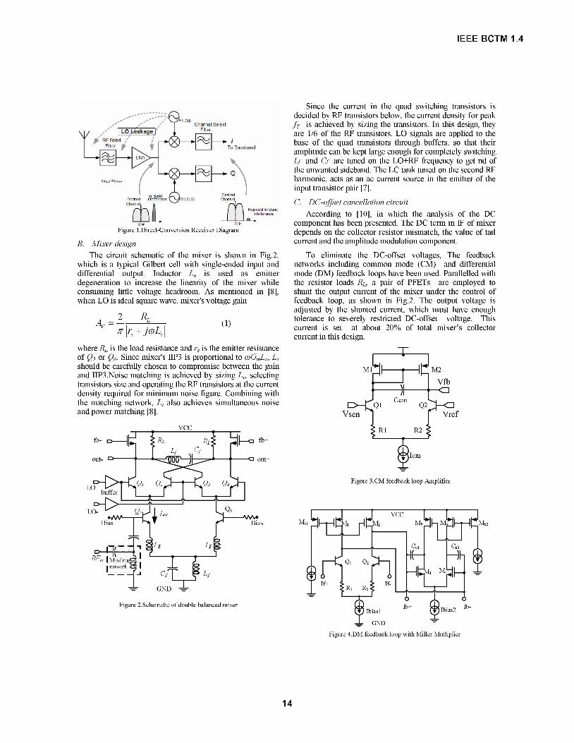
Direct-conversion receivers shown in Fig. 1 have attracteda great deal of attention over the past a few years. In actualdirect conversion systems, the LO frequency is in the middleof the RF spectrum under consideration. The higherfrequency components at the output can be easily removedby active or passive low-pass filter at the baseband. Byeliminating IF stages and the image-reject requirement of thefront-end filters, direct-conversion architecture cansignificantly improve on-chip integration of the receiver.However, this architecture creates additional performancecriteria such as DC- offsets, second order intermodulations(IM2), in-band local oscillator (LO) radiation and flickernoise that are not presented in a heterodyne counterpart.
F.F.Dai, R.C.JaegerDepartment of Electrical & Computer Engineering
Auburn UniversityAuburn, Alabama, USAdaifaO I &auburn.edu
As shown in Fig. 1, LO leakage exists from the LO portto the LNA input, mixer input, the antenna and a finiteamount of feedthrough because of substrate coupling andbond wire coupling [3]. One of the most challenges of theseperformance criteria is the effective cancellation ofDC-offsets.This paper describes a solution of DC-offsetcancellation in a 5GHz direct-conversion receiver.
In direct-conversion receiver, the down-convertedspectrum is centered at OHz. If information containsDC-offset, the SNR will be degraded. In fact, the offset maybe larger than the signal and much larger than thermal orflicker noise. A down-converted signal may have anamplitude of a few hundred microvolts while the DC-offsetmay be in the range of millivolts, which will degrade thefollowing stages [5].
There are two common DC-offset cancellationsolutions:(l)AC coupling (high pass filter) [6].(2) Digitalcancellation with DAC sampling [7]. By the means of ACcoupling, a very low corner frequency of the high pass filteris required, indicating large capacitors, which is not suitablefor integration. Digital solution including DAC willcomplicate the design and increase the power dissipation.
The work of this paper focuses on mixer compliant withIEEE 802.11a wireless LAN standard , which eliminatesDC-offset in the mixer output by analog feedback loopsmentioned firstly by P. Laferriere[5], whose design has alittle lack for not being completely implemented. Section IIpresents mixer and DC-offset cancellation circuit topology.Section III shows the experimental results. Section IVsummarized the work.
II. CIRCUIT TOPOLOGY
A. Topology previewA full direct-conversion receiver topology is illustrated in
Fig. 1. In this solution, the mixer is the primary block, and theDC-offset circuit occurs in the baseband section followingthe mixer.
1-4244-1018-5/07/$25.00 ©2007 IEEE 13
IEEE BCTM 1.4
a= 1 t %4 11 17~~~~~~o Ba§ebJahdCa Lb O- RF
in-Band A DesiredDesired Inefefreric lO(Q) Channel,Channel,.r
1L ffitalea~~~~~~~~~~~~~rencFigure I.Direct-Conversion Receiver Diagram
B. Mixer designThe circuit schematic of the mixer is shown in Fig.2,
which is a typical Gilbert cell with single-ended input anddifferential output. Inductor L, is used as emitterdegeneration to increase the linearity of the mixer whileconsuming little voltage headroom. As mentioned in [8],when LO is ideal square wave, mixer's voltage gain
_ 2 RLT Ire + jct)Le
(1)
Since the current in the quad switching transistors isdecided by RF transistors below, the current density for peakfT is achieved by sizing the transistors. In this design, theyare 1/6 of the RF transistors. LO signals are applied to thebase of the quad transistors through buffers, so that theiramplitude can be kept large enough for completely switching.Lf and Cf are tuned on the LO+RF frequency to get rid ofthe unwanted sideband. The LC tank tuned on the second RFharmonic, acts as an ac current source in the emitter of theinput transistor pair [7].
C. DC-offset cancellation circuitAccording to [10], in which the analysis of the DC
component has been presented. The DC term in IF of mixerdepends on the collector resistor mismatch, the value of tailcurrent and the amplitude modulation component.
To eliminate the DC-offset voltages, The feedbacknetworks including common mode (CM) and differentialmode (DM) feedback loops have been used. Parallelled withthe resistor loads RL, a pair of PFETs are employed toshunt the output current of the mixer under the control offeedback loop, as shown in Fig.2. The output voltage isadjusted by the shunted current, which must have enoughtolerance to severely restricted DC-offset voltage. Thiscurrent is set at about 20% of total mixer's collectorcurrent in this design.
where RL is the load resistance and r, is the emitter resistanceof Q5 or Q6. Since mixer's IIP3 is proportional to o)GmLe, Leshould be carefully chosen to compromise between the gainand IIP3.Noise matching is achieved by sizing Le, selectingtransistors size and operating the RF transistors at the currentdensity required for minimum noise figure. Combining withthe matching network, Le also achieves simultaneous noiseand power matching [8].
fbl
Out4
Figure 3.CM feedback loop Amplifier
Mbl
Figure 2.Schematic of double balanced mixer
_- GND
Figure 4.DM feedback loop with Miller Multiplier
14

IEEE BCTM 1.4
In the common-mode feedback loop, the common-modeoutput voltage is compared with a reference voltage. Thecomparison voltage controls the gate of the PFETs in orderto stabilize the common-mode voltage at the mixer output.The mixer load DC point is be stabilized by the way, toreduce the DC-offset voltage. The schematic topology isshown in Fig.3.
In the Gilbert-cell based mixer, differential-modeDC-offset is predominant at the output. The DM feedbackloop circuit is restricted not only by the baseband signalspectral, but also the noise contributing to the whole receiver.Therefore, the DM DC-offset correction loop amplifier mustfulfill 3 requirements:
* The loop must have sufficient gain at DC to provideadequate DC-offset reduction.
* The equivalent output noise of the circuit must below enough to avoid degrading the mixer noisefigure remarkably.
* The loop must have gain low enough near the lowercorner frequency of the sub channel (at frequenciesabove 150kHz in this case) where the desired signalis not attenuated significantly.
Following these requests, the differential-mode loop is a
low pass filter with high gain and low cut off frequency. Theschematic of the loop is shown in Fig.4.
The first stage illustrated in Fig.4 utilizes bipolartransistors in the feedback amplifier, which have higher gainand lower noise than MOSFETs. However, in the secondstage, a pair of MOSFETs is placed, which generates a
Miller Multiplication with high input impedance. The twostages loop amplifiers are loaded by PMOS current sources.
The total impedance seen at the output is equal to rO11rO2,and the gain is given by:
Gain g (r 1/rH2) (2)The gain of first stage is 40.3dB at OHz, the phase margin
is equal to 1300. Without the Miller capacitor, bandwidthof the amplifier is about 7MHz, and the second stage gain is45dB.
The second stage gain is similar to the first stage, whichallows the Miller effect to generate an effective capacitanceat the inter-stage of amplifier. The Miller effectivecapacitance is mostly equal to the product of thecompensation capacitance and the second stage gain.
CMiller = GainsecCui (3)
The configuration is a Miller Integrator with 2pFcapacitor which is small enough to be integrated on chip, andthe actual effective input capacitance is about lnF. It is hardto fabricate a capacitor of lnF since the capacitor is an
area-consuming component. The curve illustrated in Fig.4shows the AC response of the differential feedback-loop,which is close to the ideal model of former requests. Withthe Miller capacitor, the feedback loop has gain low enough
at 150 KHz, which offers corner frequency enough low for802.1la standard. In Fig.3, the R1 and R2 are a couple pairwith emitter degeneration to adjust the gain.
III. EXPERIMENTAL RESULTS
50 -
40 -
30 -
m 20-
.- 10-
0 -
-10 -
........~~~~~~~
10 100 1k 10k 100k 1M 1oM 100N
Freq(Hz)
Figure.5 Measured Frequency Response of the DM feedback-loop
dB Compression Point= 2dBBm
CL
-5 -35a
-45
-50~35 -3W
Figure. 7
co
CDUm_R
aJ).0_>
-25 -D -15 -10 -5 0Input Power(dBm)
Measured Input I dB Compression Point
5.10 5.12 5.14 5.16
Frequency (GHz)5.18 5.20
Figure.8 Measured Conversion Voltage GainFig.6 gives the mixer output spectrum at input RF
frequency 5.15GHz and LO frequency 5.2GHz. Fig.7 showsthe 1dB compression point with the same RF and LOfrequency above and with the load 50Q. The figure shows
15
12
6UA~~~~
3 - Simulated Result-A- Measured Result
O C
,20
-Measured Result-o- Simulated Result
-10
I-1S
-40
5
IEEE BCTM 1.4
the 1dB compression point is -2dBm, which is slightly lessthan the simulated result (-1.5dBm). In fact, the next stagehas an input resistance larger than 50Q, together with thenon-perfect input matching, which will result in the 1dBcompression point lower than test result. Fig.8 shows theconversion voltage gain versus the input signal frequency.The measured result, already computed with a large roadresistance, is smaller than simulation, which might be theinfluence of the input matching and parasitical componentsof the circuit. The measured frequency response of DC-offsetcancellation the feedback loop is close to the simulationresult, which is illustrated in Fig.5. The DC-offset voltage isless than 2 mV at mixer IF output after a pair of capacitors.
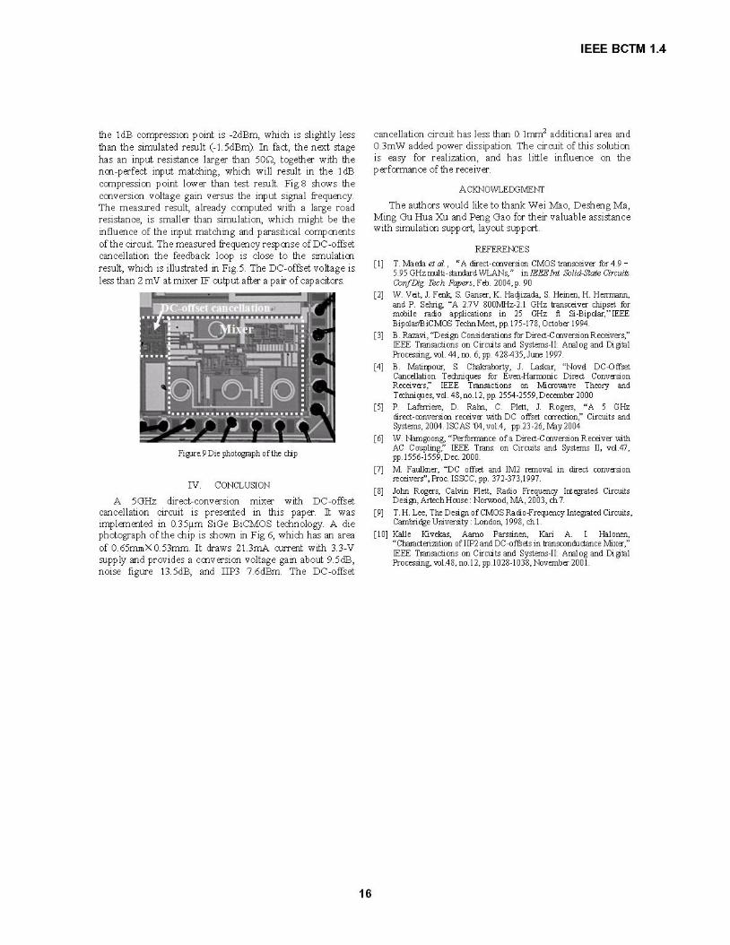
Figure.9 Die photograph of the chip
IV. CONCLUSIONA 5GHz direct-conversion mixer with DC-offset
cancellation circuit is presented in this paper. It wasimplemented in 0.35ptm SiGe BiCMOS technology. A diephotograph of the chip is shown in Fig.6, which has an areaof 0.65mmX 0.53mm. It draws 21.3mA current with 3.3-Vsupply and provides a conversion voltage gain about 9.5dB,noise figure 13.5dB, and IIP3 7.6dBm. The DC-offset
cancellation circuit has less than 0.1mm2 additional area and0.3mW added power dissipation. The circuit of this solutionis easy for realization, and has little influence on theperformance of the receiver.
ACKNOWLEDGMENT
The authors would like to thank Wei Mao, Desheng Ma,Ming Gu Hua Xu and Peng Gao for their valuable assistancewith simulation support, layout support.
REFERENCES
[1] T. Maeda et al., "A direct-conversion CMOS transceiver for 4.9 -
5.95 GHz multi-standard WLANs," inIEEEInt. Solid-State CircuitsConfDig. Tech. Papers, Feb. 2004, p. 90
[2] W. Veit, J. Fenk, S. Ganser, K. Hadjizada, S. Heinen, H. Herrmann,and P. Sehrig, "A 2.7V 800MHz-2.1 GHz transceiver chipset formobile radio applications in 25 GHz ft Si-Bipolar,"IEEEBipolar/BiCMOS Techn.Meet, pp.175-178, October 1994.
[3] B. Razavi, "Design Considerations for Direct-Conversion Receivers,"IEEE Transactions on Circuits and Systems-II: Analog and DigitalProcessing, vol. 44, no. 6, pp. 428-435, June 1997.
[4] B. Matinpour, S. Chakraborty, J. Laskar, "Novel DC-OffsetCancellation Techniques for Even-Hannonic Direct ConversionReceivers," IEEE Transactions on Microwave Theory andTechniques, vol. 48, no. 12, pp. 2554-2559, December 2000
[5] P. Laferriere, D. Rahn, C. Plett, J. Rogers, "A 5 GHzdirect-conversion receiver with DC offset correction," Circuits andSystems, 2004. ISCAS '04, vol.4, pp.23-26, May 2004
[6] W. Namgoong, "Performance of a Direct-Conversion Receiver withAC Coupling," IEEE Trans. on Circuits and Systems II, vol.47,pp.1556-1559, Dec. 2000.
[7] M. Faulkner, "DC offset and IM2 removal in direct conversionreceivers", Proc. ISSCC, pp. 372-373,1997.
[8] John Rogers, Calvin Plett, Radio Frequency Integrated CircuitsDesign, Artech House: Norwood, MA, 2003, ch.7.
[9] T. H. Lee, The Design ofCMOS Radio-Frequency Integrated Circuits,Cambridge University: London, 1998, ch.1.
[10] Kalle Kivekas, Aarno Parssinen, Kari A. I. Halonen,"Characterization of IIP2 and DC-offsets in transconductance Mixer,"IEEE Transactions on Circuits and Systems-II: Analog and DigitalProcessing, vol.48, no.12, pp.1028-1038, November 2001.
16